CN101844440A - Jet head liquid, liquid injection apparatus and actuator - Google Patents
Jet head liquid, liquid injection apparatus and actuator Download PDFInfo
- Publication number
- CN101844440A CN101844440A CN201010143229A CN201010143229A CN101844440A CN 101844440 A CN101844440 A CN 101844440A CN 201010143229 A CN201010143229 A CN 201010143229A CN 201010143229 A CN201010143229 A CN 201010143229A CN 101844440 A CN101844440 A CN 101844440A
- Authority
- CN
- China
- Prior art keywords
- piezoelectric body
- body layer
- electrode
- crystal
- jet head
- Prior art date
- Legal status (The legal status is an assumption and is not a legal conclusion. Google has not performed a legal analysis and makes no representation as to the accuracy of the status listed.)
- Pending
Links
- 239000007788 liquid Substances 0.000 title claims abstract description 38
- 238000002347 injection Methods 0.000 title claims abstract description 11
- 239000007924 injection Substances 0.000 title claims abstract description 11
- 239000010936 titanium Substances 0.000 claims abstract description 75
- 239000013078 crystal Substances 0.000 claims abstract description 38
- 239000000758 substrate Substances 0.000 claims abstract description 35
- 229910052719 titanium Inorganic materials 0.000 claims abstract description 19
- RTAQQCXQSZGOHL-UHFFFAOYSA-N Titanium Chemical compound [Ti] RTAQQCXQSZGOHL-UHFFFAOYSA-N 0.000 claims abstract description 13
- 229910052726 zirconium Inorganic materials 0.000 claims abstract description 11
- VSZWPYCFIRKVQL-UHFFFAOYSA-N selanylidenegallium;selenium Chemical compound [Se].[Se]=[Ga].[Se]=[Ga] VSZWPYCFIRKVQL-UHFFFAOYSA-N 0.000 claims abstract description 8
- QCWXUUIWCKQGHC-UHFFFAOYSA-N Zirconium Chemical compound [Zr] QCWXUUIWCKQGHC-UHFFFAOYSA-N 0.000 claims abstract description 5
- 239000000463 material Substances 0.000 claims description 17
- 229910052451 lead zirconate titanate Inorganic materials 0.000 claims description 14
- 230000015572 biosynthetic process Effects 0.000 claims description 9
- HFGPZNIAWCZYJU-UHFFFAOYSA-N lead zirconate titanate Chemical compound [O-2].[O-2].[O-2].[O-2].[O-2].[Ti+4].[Zr+4].[Pb+2] HFGPZNIAWCZYJU-UHFFFAOYSA-N 0.000 claims description 6
- 230000009466 transformation Effects 0.000 claims description 5
- 238000006073 displacement reaction Methods 0.000 abstract description 12
- 239000000976 ink Substances 0.000 description 21
- 239000012212 insulator Substances 0.000 description 17
- 238000000034 method Methods 0.000 description 17
- 230000035882 stress Effects 0.000 description 17
- 239000002243 precursor Substances 0.000 description 13
- 230000006835 compression Effects 0.000 description 11
- 238000007906 compression Methods 0.000 description 11
- 238000002425 crystallisation Methods 0.000 description 11
- 230000008025 crystallization Effects 0.000 description 11
- RKTYLMNFRDHKIL-UHFFFAOYSA-N copper;5,10,15,20-tetraphenylporphyrin-22,24-diide Chemical compound [Cu+2].C1=CC(C(=C2C=CC([N-]2)=C(C=2C=CC=CC=2)C=2C=CC(N=2)=C(C=2C=CC=CC=2)C2=CC=C3[N-]2)C=2C=CC=CC=2)=NC1=C3C1=CC=CC=C1 RKTYLMNFRDHKIL-UHFFFAOYSA-N 0.000 description 9
- 230000001681 protective effect Effects 0.000 description 9
- 238000005755 formation reaction Methods 0.000 description 8
- 238000004519 manufacturing process Methods 0.000 description 8
- 239000012528 membrane Substances 0.000 description 8
- BASFCYQUMIYNBI-UHFFFAOYSA-N platinum Chemical compound [Pt] BASFCYQUMIYNBI-UHFFFAOYSA-N 0.000 description 7
- WFKWXMTUELFFGS-UHFFFAOYSA-N tungsten Chemical compound [W] WFKWXMTUELFFGS-UHFFFAOYSA-N 0.000 description 7
- 229910052721 tungsten Inorganic materials 0.000 description 7
- 239000010937 tungsten Substances 0.000 description 7
- 238000005238 degreasing Methods 0.000 description 6
- 239000000203 mixture Substances 0.000 description 6
- 238000005245 sintering Methods 0.000 description 6
- 238000001035 drying Methods 0.000 description 5
- 239000012530 fluid Substances 0.000 description 5
- 239000007921 spray Substances 0.000 description 5
- 238000004544 sputter deposition Methods 0.000 description 5
- MCMNRKCIXSYSNV-UHFFFAOYSA-N Zirconium dioxide Chemical compound O=[Zr]=O MCMNRKCIXSYSNV-UHFFFAOYSA-N 0.000 description 4
- 239000011248 coating agent Substances 0.000 description 4
- 238000000576 coating method Methods 0.000 description 4
- 230000004048 modification Effects 0.000 description 4
- 238000012986 modification Methods 0.000 description 4
- PXHVJJICTQNCMI-UHFFFAOYSA-N Nickel Chemical compound [Ni] PXHVJJICTQNCMI-UHFFFAOYSA-N 0.000 description 3
- 229910052741 iridium Inorganic materials 0.000 description 3
- GKOZUEZYRPOHIO-UHFFFAOYSA-N iridium atom Chemical compound [Ir] GKOZUEZYRPOHIO-UHFFFAOYSA-N 0.000 description 3
- 229910044991 metal oxide Inorganic materials 0.000 description 3
- 150000004706 metal oxides Chemical class 0.000 description 3
- 229910021421 monocrystalline silicon Inorganic materials 0.000 description 3
- 230000010287 polarization Effects 0.000 description 3
- 230000008569 process Effects 0.000 description 3
- 238000007789 sealing Methods 0.000 description 3
- 238000003980 solgel method Methods 0.000 description 3
- CPLXHLVBOLITMK-UHFFFAOYSA-N Magnesium oxide Chemical compound [Mg]=O CPLXHLVBOLITMK-UHFFFAOYSA-N 0.000 description 2
- 230000008859 change Effects 0.000 description 2
- 239000000470 constituent Substances 0.000 description 2
- 239000003989 dielectric material Substances 0.000 description 2
- 239000010931 gold Substances 0.000 description 2
- 238000010884 ion-beam technique Methods 0.000 description 2
- 229910052746 lanthanum Inorganic materials 0.000 description 2
- 230000007246 mechanism Effects 0.000 description 2
- 229910052751 metal Inorganic materials 0.000 description 2
- 239000002184 metal Substances 0.000 description 2
- 229910052697 platinum Inorganic materials 0.000 description 2
- 239000002904 solvent Substances 0.000 description 2
- 238000000018 DNA microarray Methods 0.000 description 1
- VYPSYNLAJGMNEJ-UHFFFAOYSA-N Silicium dioxide Chemical compound O=[Si]=O VYPSYNLAJGMNEJ-UHFFFAOYSA-N 0.000 description 1
- XUIMIQQOPSSXEZ-UHFFFAOYSA-N Silicon Chemical compound [Si] XUIMIQQOPSSXEZ-UHFFFAOYSA-N 0.000 description 1
- 238000002441 X-ray diffraction Methods 0.000 description 1
- FOLMBQLGENFKLO-UHFFFAOYSA-N [Pb].[Mg].[Nb] Chemical compound [Pb].[Mg].[Nb] FOLMBQLGENFKLO-UHFFFAOYSA-N 0.000 description 1
- 239000002253 acid Substances 0.000 description 1
- 229910021523 barium zirconate Inorganic materials 0.000 description 1
- DQBAOWPVHRWLJC-UHFFFAOYSA-N barium(2+);dioxido(oxo)zirconium Chemical compound [Ba+2].[O-][Zr]([O-])=O DQBAOWPVHRWLJC-UHFFFAOYSA-N 0.000 description 1
- 239000007767 bonding agent Substances 0.000 description 1
- 238000001816 cooling Methods 0.000 description 1
- 230000000694 effects Effects 0.000 description 1
- 239000007772 electrode material Substances 0.000 description 1
- 238000005516 engineering process Methods 0.000 description 1
- 230000006355 external stress Effects 0.000 description 1
- 239000011521 glass Substances 0.000 description 1
- 239000002241 glass-ceramic Substances 0.000 description 1
- PCHJSUWPFVWCPO-UHFFFAOYSA-N gold Chemical compound [Au] PCHJSUWPFVWCPO-UHFFFAOYSA-N 0.000 description 1
- 229910052737 gold Inorganic materials 0.000 description 1
- 238000010438 heat treatment Methods 0.000 description 1
- FZLIPJUXYLNCLC-UHFFFAOYSA-N lanthanum atom Chemical compound [La] FZLIPJUXYLNCLC-UHFFFAOYSA-N 0.000 description 1
- 229910052745 lead Inorganic materials 0.000 description 1
- 238000011068 loading method Methods 0.000 description 1
- 229910052749 magnesium Inorganic materials 0.000 description 1
- 239000011777 magnesium Substances 0.000 description 1
- 239000000395 magnesium oxide Substances 0.000 description 1
- 238000005259 measurement Methods 0.000 description 1
- 229910052759 nickel Inorganic materials 0.000 description 1
- 229910000480 nickel oxide Inorganic materials 0.000 description 1
- 229910052758 niobium Inorganic materials 0.000 description 1
- 239000010955 niobium Substances 0.000 description 1
- 229910000484 niobium oxide Inorganic materials 0.000 description 1
- URLJKFSTXLNXLG-UHFFFAOYSA-N niobium(5+);oxygen(2-) Chemical compound [O-2].[O-2].[O-2].[O-2].[O-2].[Nb+5].[Nb+5] URLJKFSTXLNXLG-UHFFFAOYSA-N 0.000 description 1
- 239000005416 organic matter Substances 0.000 description 1
- GNRSAWUEBMWBQH-UHFFFAOYSA-N oxonickel Chemical compound [Ni]=O GNRSAWUEBMWBQH-UHFFFAOYSA-N 0.000 description 1
- 239000000700 radioactive tracer Substances 0.000 description 1
- 238000004151 rapid thermal annealing Methods 0.000 description 1
- 229910052710 silicon Inorganic materials 0.000 description 1
- 239000010703 silicon Substances 0.000 description 1
- 239000000243 solution Substances 0.000 description 1
- 229910001220 stainless steel Inorganic materials 0.000 description 1
- 239000010935 stainless steel Substances 0.000 description 1
- 239000000126 substance Substances 0.000 description 1
- 230000001360 synchronised effect Effects 0.000 description 1
- 229910052715 tantalum Inorganic materials 0.000 description 1
- GUVRBAGPIYLISA-UHFFFAOYSA-N tantalum atom Chemical compound [Ta] GUVRBAGPIYLISA-UHFFFAOYSA-N 0.000 description 1
- 238000003466 welding Methods 0.000 description 1
Images


Classifications
-
- B—PERFORMING OPERATIONS; TRANSPORTING
- B41—PRINTING; LINING MACHINES; TYPEWRITERS; STAMPS
- B41J—TYPEWRITERS; SELECTIVE PRINTING MECHANISMS, i.e. MECHANISMS PRINTING OTHERWISE THAN FROM A FORME; CORRECTION OF TYPOGRAPHICAL ERRORS
- B41J2/00—Typewriters or selective printing mechanisms characterised by the printing or marking process for which they are designed
- B41J2/005—Typewriters or selective printing mechanisms characterised by the printing or marking process for which they are designed characterised by bringing liquid or particles selectively into contact with a printing material
- B41J2/01—Ink jet
- B41J2/135—Nozzles
- B41J2/14—Structure thereof only for on-demand ink jet heads
- B41J2/14201—Structure of print heads with piezoelectric elements
- B41J2/14233—Structure of print heads with piezoelectric elements of film type, deformed by bending and disposed on a diaphragm
-
- B—PERFORMING OPERATIONS; TRANSPORTING
- B41—PRINTING; LINING MACHINES; TYPEWRITERS; STAMPS
- B41J—TYPEWRITERS; SELECTIVE PRINTING MECHANISMS, i.e. MECHANISMS PRINTING OTHERWISE THAN FROM A FORME; CORRECTION OF TYPOGRAPHICAL ERRORS
- B41J2/00—Typewriters or selective printing mechanisms characterised by the printing or marking process for which they are designed
- B41J2/005—Typewriters or selective printing mechanisms characterised by the printing or marking process for which they are designed characterised by bringing liquid or particles selectively into contact with a printing material
- B41J2/01—Ink jet
- B41J2/135—Nozzles
- B41J2/16—Production of nozzles
- B41J2/1607—Production of print heads with piezoelectric elements
- B41J2/161—Production of print heads with piezoelectric elements of film type, deformed by bending and disposed on a diaphragm
-
- B—PERFORMING OPERATIONS; TRANSPORTING
- B41—PRINTING; LINING MACHINES; TYPEWRITERS; STAMPS
- B41J—TYPEWRITERS; SELECTIVE PRINTING MECHANISMS, i.e. MECHANISMS PRINTING OTHERWISE THAN FROM A FORME; CORRECTION OF TYPOGRAPHICAL ERRORS
- B41J2/00—Typewriters or selective printing mechanisms characterised by the printing or marking process for which they are designed
- B41J2/005—Typewriters or selective printing mechanisms characterised by the printing or marking process for which they are designed characterised by bringing liquid or particles selectively into contact with a printing material
- B41J2/01—Ink jet
- B41J2/135—Nozzles
- B41J2/16—Production of nozzles
- B41J2/1621—Manufacturing processes
- B41J2/164—Manufacturing processes thin film formation
- B41J2/1646—Manufacturing processes thin film formation thin film formation by sputtering
-
- H—ELECTRICITY
- H10—SEMICONDUCTOR DEVICES; ELECTRIC SOLID-STATE DEVICES NOT OTHERWISE PROVIDED FOR
- H10N—ELECTRIC SOLID-STATE DEVICES NOT OTHERWISE PROVIDED FOR
- H10N30/00—Piezoelectric or electrostrictive devices
- H10N30/20—Piezoelectric or electrostrictive devices with electrical input and mechanical output, e.g. functioning as actuators or vibrators
- H10N30/204—Piezoelectric or electrostrictive devices with electrical input and mechanical output, e.g. functioning as actuators or vibrators using bending displacement, e.g. unimorph, bimorph or multimorph cantilever or membrane benders
- H10N30/2047—Membrane type
-
- H—ELECTRICITY
- H10—SEMICONDUCTOR DEVICES; ELECTRIC SOLID-STATE DEVICES NOT OTHERWISE PROVIDED FOR
- H10N—ELECTRIC SOLID-STATE DEVICES NOT OTHERWISE PROVIDED FOR
- H10N30/00—Piezoelectric or electrostrictive devices
- H10N30/80—Constructional details
- H10N30/85—Piezoelectric or electrostrictive active materials
- H10N30/853—Ceramic compositions
- H10N30/8548—Lead based oxides
- H10N30/8554—Lead zirconium titanate based
Abstract
The object of the present invention is to provide a kind of jet head liquid, liquid injection apparatus and actuator that has improved the displacement properties of piezoelectric element.This jet head liquid possesses: stream forms substrate (10), and it is formed with the pressure generating chamber that is connected with nozzle (21); And piezoelectric element (300), it makes pressure generating chamber produce the pressure variation, this piezoelectric element (300) comprises the piezoelectric body layer (70) that contains titanium (Ti) and zirconium (Zr) and is separately positioned on first electrode (60) and second electrode (80) of the both sides of this piezoelectric body layer (70), wherein, in the piezoelectric body layer (70) the ratio of component Ti/ (Zr+Ti) of contained zirconium and titanium in the scope more than 0.50 and below 0.60 and piezoelectric body layer (70) be formed at the crystal that part on first electrode (60) contains rhombohedral system at least.
Description
Technical field
The present invention relates to displacement by piezoelectric element from jet head liquid, the liquid injection apparatus of jet droplets and the actuator that possesses piezoelectric element.
Background technology
As the representation example of jet head liquid, can enumerate by utilizing pressure generating mechanism to make generation pressure in the pressure generating chamber from the ink jet recording head of nozzle ejection ink droplet.As the pressure generating mechanism that constitutes this ink jet recording head, can enumerate the piezoelectric element that for example forms by 2 electrode clamping piezoelectric body layers, thereby to giving pressure in the pressure generating chamber drops out from nozzles is ejected by making this piezoelectric element deflection deformation, wherein this piezoelectric body layer comprises the piezoelectric that presents the electromechanical transformation.
And, as employed piezoelectric body layer in such piezoelectric element, proposition has following proposal: for example contain titanium (Ti) and zirconium (Zr), its element is 0.5~0.8 than (ratio of component) Zr/ (Zr+Ti), and its crystallization is monoclinic system (for example with reference to a patent documentation 1).
In addition, as piezoelectric body layer, proposing has following proposal: for example contain titanium (Ti) and zirconium (Zr), its crystallization is tetragonal system (for example with reference to a patent documentation 2) when its element is 0.50 left and right sides than (ratio of component) Zr/ (Zr+Ti).
Here, known: as to comprise that lead zirconate titanate (PZT) for example etc. has the system of crystallization of piezoelectric body layer of the material of perovskite structure, generally by the ratio of component decision of Ti and Zr.For example, known: promptly piezoelectric body layer is not applied under the situation of the piezoelectric body layer of the PZT that comprises piece (バ Le Network) external stress also not by the situation of constraints such as substrate under, at ratio of component Ti/ (Zr+Ti) is about more than 0.50 when (ratio of component Zr/ (Zr+Ti) is less than about 0.50), the system of crystallization of piezoelectric body layer becomes tetragonal system, at ratio of component less than becoming rhombohedral system or monoclinic system at about 0.50 o'clock.That is, known: it is near 0.50 that the accurate homotype phase boundary (MPB) that comprises the tetragonal system of piezoelectric body layer of PZT and rhombohedral system is present in ratio of component Ti/ (Zr+Ti).
Patent documentation 1: the spy opens the 2007-088446 communique
Patent documentation 2: the spy opens the 2005-119166 communique
The piezoelectric property of piezoelectric body layer changes according to the composition of piezoelectric body layer, but also changes according to the system of crystallization of piezoelectric body layer.But, constitute the system of crystallization of the piezoelectric body layer of piezoelectric element as mentioned above, depend on the composition of piezoelectric body layer usually.As above-mentioned patent documentation is put down in writing, the composition and/or the system of crystallization of piezoelectric body layer proposed various schemes, but all be the scheme that the system of crystallization of piezoelectric body layer depends on the composition of piezoelectric body layer.In addition, because the composition of piezoelectric body layer for example is subjected to the restriction of relation etc. of the lattice paprmeter of the lattice paprmeter of piezoelectric body layer and substrate, so its adjusting range is restricted, and the characteristic of resulting piezoelectric body layer is also limited.Therefore, be difficult to realize raising by the further displacement properties of the piezoelectric element that piezoelectric property obtained of piezoelectric body layer.And then in recent years, expectation realizes the further raising of the displacement properties of piezoelectric element, but satisfies such difficulty that is contemplated to be.
In addition, such problem is not limited to the employed piezoelectric element of ink jet recording head, and also be present in the employed piezoelectric element of the jet head liquid that sprays other drops, and then be present in too in the jet head liquid employed actuator of device in addition.
Summary of the invention
The present invention realizes that in view of such situation its purpose is to provide a kind of jet head liquid, liquid injection apparatus and actuator that has improved the displacement properties of piezoelectric element.
What address the above problem the invention reside in a kind of jet head liquid, and it possesses: stream forms substrate, and it is formed with the pressure generating chamber that is connected with the nozzle of liquid droplets; And piezoelectric element, it is arranged on this stream formation substrate and makes described pressure generating chamber produce pressure and changes, this piezoelectric element comprises the piezoelectric body layer that contains titanium (Ti) and zirconium (Zr) and is separately positioned on first electrode and second electrode of the both sides of this piezoelectric body layer, wherein, in the described piezoelectric body layer ratio of component Ti/ (Zr+Ti) of contained zirconium and titanium in the scope more than 0.50 and below 0.60 and this piezoelectric body layer contain the crystal of rhombohedral system.And the crystal of contained rhombohedral system in the described piezoelectric body layer particularly, is to make the crystal that tetragonal crystal-phase transformation forms owing to the stress that is subjected to from basalis.
In the present invention, because said components is than in preset range, institute is so that the distortion when the dielectric constant step-down of piezoelectric body layer and polarization rotation becomes greatly.In addition because piezoelectric body layer contains the crystal of rhombohedral system, so that the displacement of piezoelectric body layer is big relatively.Therefore, can improve the deformation characteristics such as addendum modification of piezoelectric element.In addition, can reduce the voltage that piezoelectric element is applied and the load of supply unit is reduced.
Here, preferred, be under the situation of the layer that forms of the piezoelectric body film of stacked multilayer at described piezoelectric body layer, the outermost at least described piezoelectric body film that described stream forms substrate-side comprises the crystal of rhombohedral system.Thus, can improve the displacement properties of piezoelectric element more reliably.
In addition, preferred, described piezoelectric body layer is formed by the material with perovskite structure, for example lead zirconate titanate (PZT).Under the situation that piezoelectric body layer is formed by such material, the displacement properties of piezoelectric element improves significantly.
And, the invention reside in a kind of liquid injection apparatus, it possesses jet head liquid as described above.In this invention, can realize having improved the liquid injection apparatus of the spray characteristic of drop.
In addition, the invention reside in a kind of actuator, it possesses piezoelectric element, first electrode and second electrode that it comprises the piezoelectric body layer that contains titanium (Ti) and zirconium (Zr) and is separately positioned on the both sides of this piezoelectric body layer, wherein, the ratio of component Ti/ (Zr+Ti) of contained zirconium and titanium is more than 0.50 and 0.60 following and this piezoelectric body layer contains the crystal of rhombohedral system in the described piezoelectric body layer.
In the present invention, because said components is than in preset range, institute is so that the distortion when the dielectric constant step-down of piezoelectric body layer and polarization rotation becomes greatly.In addition because piezoelectric body layer contains the crystal of rhombohedral system, so that the displacement of piezoelectric body layer is big relatively.Therefore, can improve the deformation characteristics such as addendum modification of piezoelectric element.In addition, can reduce the voltage that piezoelectric element is applied and the load of supply unit is reduced.
Description of drawings
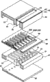
Fig. 1 is the exploded perspective view of schematic configuration of the record head of expression embodiment 1.
Fig. 2 is the vertical view and the profile of the record head of expression embodiment 1.
Fig. 3 is the profile of structure of the piezoelectric element of expression embodiment 1.
Fig. 4 is the profile of manufacture method of the record head of expression embodiment 1.
Fig. 5 is the profile of manufacture method of the record head of expression embodiment 1.
Fig. 6 is the profile of manufacture method of the record head of expression embodiment 1.
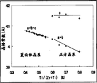
Fig. 7 is the ratio of component Ti/ (Zr+Ti) of expression piezoelectric body layer and the curve map of the relation of lattice paprmeter.
Fig. 8 is the figure of schematic configuration of the tape deck of a kind of embodiment of expression.
Symbol description
10 streams form substrate, 12 pressure generating chamber, 20 nozzle plates; 21 nozzles, 30 protective substrates, 40 flexibilities (コ Application プ ラ イ ア Application ス) substrate; 41 diaphragm seals, 42 fixed heads, 50 elastic membranes; 55 insulator films, 60 first electrodes, 61 conductive layers; 62 orientation key-courses, 70 piezoelectric body layers, 80 second electrodes; 90 lead-in wire electrodes, 300 piezoelectric elements.
The specific embodiment
Below, explain the present invention based on embodiment.
(embodiment 1)
Fig. 1 is the exploded perspective view of expression as the schematic configuration of the ink jet recording head of an example of the jet head liquid of embodiments of the present invention 1, and Fig. 2 is vertical view and the A-A ' profile thereof of Fig. 1.
The stream that constitutes ink jet recording head forms substrate 10, and for example the monocrystalline silicon substrate by face orientation (110) constitutes, and as Fig. 1 and shown in Figure 2, a plurality of pressure generating chamber 12 are arranged side by side on its width.In addition, the zone in the longitudinally outside that forms the pressure generating chamber 12 of substrate 10 at stream is formed with interconnecting part 13, and interconnecting part 13 is communicated with via black supply passageway 14 and access 15 by each pressure generating chamber's 12 setting with each pressure generating chamber 12.Interconnecting part 13 is connected with the reservoir 32 of protective substrate described later and constitutes a part as the fluid reservoir of the shared black chamber of each pressure generating chamber 12.China ink supply passageway 14 plays the flow path resistance that will flow into the China ink of pressure generating chamber 12 from interconnecting part 13 and remains certain effect, and in the present embodiment, it forms with specific pressure generation chamber 12 narrow width.
In addition, the one side side at stream formation substrate 10 has nozzle plate 20 by joints such as bonding agent and/or thermal welding films, and this nozzle plate 20 is disposed with the nozzle 21 that is connected with each pressure generating chamber 12.In addition, nozzle plate 20 is made of for example glass ceramics, monocrystalline silicon substrate, stainless steel etc.
On the other hand, on the face of a side opposite that forms substrate at such stream, be formed with the elastic membrane 50 that constitutes by oxide-film, on this elastic membrane 50, be formed with the insulator film 55 that the oxide-film by the material different with elastic membrane 50 constitutes with nozzle plate 20.And then, on this insulator film 55, be formed with the piezoelectric element 300 that constitutes by first electrode 60, piezoelectric body layer 70 and second electrode 80.In general, with a certain side's of piezoelectric element 300 electrode as a plurality of piezoelectric elements 300 shared common electrode, the opposing party's electrode and piezoelectric body layer 70 carried out in the zone relative with each pressure generating chamber 12 together that pattern forms and as absolute electrode.In the present embodiment, with the common electrode of first electrode 60,, but also can set on the contrary because of the relation of drive circuit and/or wiring the absolute electrode of second electrode 80 as piezoelectric element 300 as piezoelectric element 300.
In addition, the part that such piezoelectric element 300 and the driving by piezoelectric element 300 are taken place in displacement is that oscillating plate is collectively referred to as actuator.In above-mentioned example, elastic membrane 50, insulator film 55 and first electrode 60 play a role as oscillating plate, but the structure of oscillating plate is not particularly limited, and for example also elastic membrane 50 and insulator film 55 can be set and first electrode 60 is played a role as oscillating plate.In addition, for example also can make piezoelectric element 300 self double as oscillating plate in fact.
Here, first electrode 60 in the present embodiment, for example waits orientation key-course 62 formations that constitute by tungsten (W) by being formed at the conductive layer 61 on the insulator film 55 and being formed on the conductive layer 61.
And, piezoelectric body layer 70 be formed at the part of orientation on the key-course 62 at least, be subjected to being orientated the influence of the crystalline orientation of key-course 62, its crystal face orientation is (100).Be piezoelectric body layer 70, on orientation key-course 62, carry out epitaxial growth, thereby its crystal face orientation be (100).
In addition, piezoelectric body layer 70, the ratio of component Ti/ (Zr+Ti) of its zirconium (Zr) and titanium (Ti) and contain the crystal of rhombohedral system in the scope more than 0.50 and below 0.60.Known: in general the piezoelectric body layer that is made of the material with perovskite structure, is about 0.50 when above at its ratio of component Ti/ (Zr+Ti), and its crystal is a tetragonal system, at its ratio of component less than becoming rhombohedral system at about 0.50 o'clock.That is, under ratio of component Ti/ (Zr+Ti) is situation more than 0.50 and below 0.60, originally for containing the film of tetragonal crystal, but piezoelectric body layer of the present invention 70, become the crystal that contains rhombohedral system but not the film of tetragonal crystal.
Here, the crystal of the rhombohedral system that so-called piezoelectric body layer 70 is like this comprised, particularly, the crystal that phase transformation obtains that is piezoelectric body layer 70 owing to be subjected to from the stress of basalis.For example, in the present embodiment, be subjected to the compression stress of predetermined strength from basalis, make tetragonal crystal etc. become rhombohedral system mutually by making piezoelectric body layer 70.That is, the piezoelectric body layer 70 of present embodiment becomes following film: its ratio of component Ti/ (Zr+Ti) is not subjected to accurate homotype phase boundary (MPB) under the state of stress from basalis like that greater than the piezoelectric body layer of for example piece, and mainly comprises the crystal of rhombohedral system.In addition, the basalis of so-called piezoelectric body layer 70 is to compare the layer that forms basic 10 sides by stream with piezoelectric body layer 70, and it not only comprises orientation key-course 62 (first electrode 60), and comprises insulator film 55 etc.
In the present embodiment, by the orientation key-course 62 that is made of than piezoelectric body layer 70 little materials lattice paprmeter being set as basalis, and on this orientation key-course 62, form piezoelectric body layer 70, utilize this orientation key-course 62 and do not match (misfit) of the lattice paprmeter of piezoelectric body layer 70 to make piezoelectric body layer 70 be subjected to the compression stress of predetermined strength from basalis.The crystal that constitutes the tungsten (W) of orientation key-course 62 is the body-centered cubic crystalline substance, also has its lattice paprmeter to be
 With lattice paprmeter be
 About PZT compare very little.Therefore,
 piezoelectric body layer 70 is subjected to the compression stress of predetermined strength from orientation key-course 62, its result, and piezoelectric body layer 70 becomes the film of the crystal that mainly comprises rhombohedral system.
In addition, so-called here " lattice paprmeter " is the lattice paprmeter along the direction (a axle or b direction of principal axis) at piezoelectric body layer 70 and interface first electrode 60.
The piezoelectric body layer 70 of present embodiment as shown in Figure 3, forms by stacked multilayer (being 12 layers in the present embodiment) piezoelectric body film 71.Like this, preferred, under the situation that piezoelectric body layer 70 is made of a plurality of piezoelectric body films 71, the outermost piezoelectric body film 71a of at least the first electrode 60 sides, mainly the crystal by rhombohedral system constitutes.Especially, preferred, about 1/3 main crystal by rhombohedral system of the thickness direction of piezoelectric body layer 70 constitute.For example, in the structure of present embodiment, be provided with the orientation key-course 62 that constitutes by tungsten (W), its result, piezoelectric body film 71a~71d of about 4 layers of first electrode, 60 sides mainly is made of the crystal of rhombohedral system.
And, possess such piezoelectric body layer 70 by piezoelectric element 300, can improve the displacement properties such as addendum modification of piezoelectric element 300 significantly.When the ratio of component Ti/ of piezoelectric body layer 70 (Zr+Ti) is 0.50 when above, the dielectric constant step-down of piezoelectric body layer 70.That is, the electric capacity of piezoelectric body layer 70 diminishes.Distortion when polarization is rotated in addition increases.And then, by in piezoelectric body layer 70, comprising the crystal of rhombohedral system, make displacement become big relatively.Therefore, compare, can reduce the voltage that is applied, can alleviate the load of supply unit with piezoelectric element in the past.In addition, by applying the voltage that equates with the situation of in the past piezoelectric element, also can improve the addendum modification of piezoelectric element 300.
In addition, on each second electrode 80 as the absolute electrode of piezoelectric element 300, be connected with from draw near the end of black supply passageway 14 sides and extend be arranged on the insulator film 55, for example wait the lead-in wire electrode 90 of formation by gold (Au).
Form on the substrate 10 at the stream that is being formed with such piezoelectric element 300,, engage that have protective substrate 30, this protective substrate 30 to have to be used to protect the space of piezoelectric element 300 be piezoelectric element maintaining part 31 in the zone relative with piezoelectric element 300.In addition, on protective substrate 30, be provided with reservoir 32, this reservoir is connected with interconnecting part 13 that stream forms substrate 10 as mentioned above and constitutes the fluid reservoir 100 of the shared black chamber that becomes each pressure generating chamber 12.In addition, protective substrate 30 is provided with on thickness direction the through hole 33 that connects protective substrate 30, is set to expose in this through hole 33 near the end of the lead-in wire electrode 90 of drawing from each piezoelectric element 300.
Be fixed with the drive circuit 120 that is used to drive piezoelectric element 300 on protective substrate 30, this drive circuit 120 is electrically connected via connecting wiring 121 with lead-in wire electrode 90, and connecting wiring 121 is made of leads such as closing lines.In addition, joint has the flexible base, board 40 that comprises diaphragm seal 41 and fixed head 42 on protective substrate 30.Diaphragm seal 41 comprises that rigidity is low and has flexible material, utilizes a face of sealing film 41 sealing reservoir 32.Fixed head 42 is formed by the material of relative hard.The zone relative with fluid reservoir 100 of this fixed head 42 becomes the peristome 43 that has been removed fully on thickness direction, a face of fluid reservoir 100 only had 41 sealings of flexible diaphragm seal.
In the ink jet recording head of the present embodiment of structure as described above, obtain China ink from the black introducing port that is connected with the ink supply unit of not shown outside, after inside has been full of China ink till nozzle 21 from fluid reservoir 100, by according to tracer signal from drive circuit 120, each piezoelectric element 300 corresponding with pressure generating chamber 12 applied voltage and make it deflection deformation, spray ink droplets from nozzle 21 thereby pressure in each pressure generating chamber 12 are raise.
Below, for an example of the manufacture method of such ink jet recording head, particularly be an example of manufacture method that constitutes the piezoelectric element 300 of brake, describe.Fig. 4 to Fig. 6 is the profile of manufacture method of the ink jet recording head of expression embodiments of the present invention 1.
At first, shown in Fig. 4 (a), for example carry out thermal oxide by the stream as silicon substrate is formed substrate 10, the surface that forms substrate 10 at stream forms by silica (SiO
2) wait the elastic membrane 50 of formation.Next, shown in Fig. 4 (b), on elastic membrane 50, form by insulator films such as zirconia 55 with the thickness about 100~500nm.Next, shown in Fig. 4 (c), on insulator film 55, form first electrode 60.Particularly, at first on insulator film 55, for example form the conductive layer 61 that constitutes by platinum (Pt), iridium (Ir) etc. by sputtering method with the thickness about 20~80nm.And then, on this conductive layer 61, for example form the orientation key-course 62 that constitutes by tungsten (W) by sputtering method with the thickness about 5~20nm.
Next, form piezoelectric body layer 70.In the present embodiment, use so-called sol-gel process to form piezoelectric body layer 70, this so-called sol-gel process is dissolved metallorganic, be dispersed in the so-called colloidal sol that obtains in the solvent and make it drying and solation by coating, and then carry out sintering with high temperature, obtain comprising the piezoelectric body layer 70 of metal oxide.In addition, the manufacture method of piezoelectric body layer 70 is not limited to sol-gel process, also can adopt MOD (Metal OrganicDecomposition, metallorganic decomposes) method and/or sputtering method etc.
As the concrete formation step of piezoelectric body layer 70, at first, shown in Fig. 5 (a), on first electrode 60, form piezoelectrics precursor film 72 as the precursor film of piezoelectric body layer 70.That is, on orientation key-course 62, apply the colloidal sol (solution) (working procedure of coating) that contains Ti and Zr.Then, this piezoelectrics precursor film 72 is heated to predetermined temperature, makes its dry certain hour (drying process).For example, by piezoelectrics precursor film 72 was kept 5~10 minutes down at 150~170 ℃, can make its drying.Next, by with drying piezoelectrics precursor film 72 be heated to predetermined temperature and keep certain hour, make its degreasing (degreasing process).For example, by piezoelectrics precursor film 72 being heated to the temperature about 300~400 ℃ and keeping about 5~10 minutes, can make its degreasing.In addition, so-called here degreasing is instigated organic principle contained in the piezoelectrics precursor film 72 to break away from and is for example NO
2, CO
2, H
2O etc.In addition, preferred in degreasing process, programming rate is made as more than 15 ℃/second.
Next, shown in Fig. 5 (b), by piezoelectrics precursor film 72 is heated to predetermined temperature and keeps certain hour to make it crystallization, thereby form the piezoelectric body film 71a (sintering circuit) of ground floor.Particularly, for example 72 heating 5~30 minutes of piezoelectrics precursor film are formed piezoelectric body film 71a with 650~800 ℃.In addition, preferred, programming rate at this moment is made as below 15 ℃/second.
Next, shown in Fig. 5 (c), in the piezoelectric body film 71a of ground floor had been formed on stage on first electrode 60 (orientation key-course 62), the piezoelectric body film 71a pattern with first electrode 60 and ground floor formed reservation shape simultaneously.Then, repeatedly repeat above-mentioned working procedure of coating, drying process and degreasing process, shown in Fig. 5 (d), comprising that stream above the piezoelectric body film 71a of ground floor forms the piezoelectrics precursor film 72 that forms the second layer~4th layer on the substrate 10.Then, simultaneously the piezoelectrics precursor film 72 of this multilayer is heated and make it crystallization, thereby form piezoelectric body film 71b to 71d (sintering circuit).Afterwards, the operation of the piezoelectrics precursor film 72 by repeatedly repeating to form like this multilayer and make the operation of piezoelectrics precursor film 72 crystallizations of this multilayer forms the piezoelectric body layer 70 of the piezoelectric body film 71 that comprises multilayer (being 12 layers in the present embodiment).
And, like this piezoelectric body layer 70 of Xing Chenging be formed at the part of orientation on the key-course 62 since with as not the matching of the lattice paprmeter of the orientation key-course 62 of basalis, and be subjected to the compression stress of predetermined strength from orientation key-course 62.Thus, piezoelectric body layer 70 though its ratio of component Ti/ (Zr+Ti) is more than 0.50 and below 0.60, becomes the film of the crystal that comprises rhombohedral system.In addition, the intensity of the compression stress that piezoelectric body layer 70 is suffered can for example utilize the material of orientation key-course 62 to adjust.Material as orientation key-course 62 except that tungsten (W), can also use tantalum (Ta), nickel (Ni) etc.
In addition, like this piezoelectric body layer 70 of Xing Chenging be formed at the part of orientation on the key-course 62 at least owing to be subjected to being orientated the influence of the crystalline orientation of key-course 62, its crystal face orientation is (100).That is, piezoelectric body layer 70 carry out epitaxial growth on orientation key-course 62, thereby its crystal face orientation is (100).
Afterwards, shown in Fig. 6 (a), on piezoelectric body layer 70, form second electrode 80 that for example waits formation, afterwards by iridium (Ir), shown in Fig. 6 (b), in the zone relative piezoelectric body layer 70 and second electrode 80 are carried out pattern and form and form piezoelectric element 300 with each pressure generating chamber 12.
As mentioned above, in the present embodiment, not because not matching of the lattice paprmeter of orientation key-course 62 and piezoelectric body layer 70, make piezoelectric body layer 70 be compressed stress from orientation key-course 62, but by forming basalises such as first electrode 60 and/or insulator film 55 than piezoelectric body layer 70 big predetermined materials with linear expansion coefficient, and constitute piezoelectric body layer 70 in the cooling procedure after sintering, make piezoelectric body layer 70 be subjected to the compression stress of predetermined strength from these basalises.Therefore, when making piezoelectric element 300, for example the composition of the material of the basalis by piezoelectric body layers 70 such as appropriate change first electrode 60, insulator films 55 and/or thickness, piezoelectric body layer 70 and then sintering temperature etc. are created conditions, and can adjust the intensity of the compression stress that piezoelectric body layer 70 is subjected to from basalis.That is, the intensity of the compression stress that is subjected to from basalis by suitable adjustment piezoelectric body layer 70 even its ratio of component Ti/ (Zr+Ti) is more than 0.50 and below 0.60, also can form the film of the crystal that comprises rhombohedral system.
Here, to except making ratio of component Ti/ (Zr+Ti) that the variation of the lattice paprmeter of other piezoelectric body layers 70 when making piezoelectric body layer 70 regularly of creating conditions is described.Fig. 7 is the ratio of component Ti/ (Zr+Ti) of expression piezoelectric body layer and the curve map of the relation of lattice paprmeter.
In addition, the lattice paprmeter of piezoelectric body layer, these 2 kinds measurement results of measuring means outside the plane based on X-ray diffraction method (xrd method), in the plane.In addition, piezoelectric body layer 70 following formation.At first, forming the insulator film 55 that constitutes by zirconia etc. with the thickness about 300nm on the substrate.Then, on insulator film 55 by sputtering method from lower layer side begin stacked platinum (Pt), iridium (Ir) forms conductive layer 61.The thickness of conductive layer 61 is Ir/Pt=10/50nm.And then, on this conductive layer 61,, form the orientation key-course 62 that constitutes by tungsten (W) with the thickness about 10nm by the ion beam-assisted sputtering method.By adopting the ion beam-assisted method, make the tungsten crystal on film thickness direction, carry out (100) planar orientation.Then, on this orientation key-course 62, by coating metallorganic is dissolved, is dispersed in the so-called colloidal sol that obtains in the solvent and makes it dry, under 400 ℃, make it solation afterwards, and then at 750 ℃ RTA (Rapid Thermal Anealing, rapid thermal annealing) carries out sintering under, form the piezoelectric body layer 70 that comprises metal oxide.
Shown in the curve of Fig. 7, up to the ratio of component Ti/ of piezoelectric body layer 70 (Zr+Ti) be near 0.6 till, the lattice paprmeter of a axle of crystal lattice, b axle and c axle all is roughly certain (a=b=c), when ratio of component Ti/ (Zr+Ti) is greater than 0.6 the time, the lattice paprmeter (a=b<c) of the c axle different with the lattice paprmeter of a axle and b axle has appearred.From this result as can be known, until the ratio of component Ti/ of piezoelectric body layer 70 (Zr+Ti) be near 0.60 till, piezoelectric body layer 70 all is the film that mainly comprises the crystal of rhombohedral system, when ratio of component Ti/ (Zr+Ti) greater than 0.6 the time, piezoelectric body layer 70 is for mainly comprising the film of tetragonal crystal.That is, as from this result as can be known, by adjust the intensity of piezoelectric body layer 70, can form ratio of component Ti/ (Zr+Ti) from the suffered compression stress of basalis be 0.50 or more and 0.60 below and mainly comprise the piezoelectric body layer 70 of rhombohedral system.
(other embodiments)
More than, an embodiment of the invention are illustrated, but the present invention is not limited to above-mentioned embodiment certainly.For example, in the above-described embodiment, be provided with orientation key-course 62 as first electrode 60, piezoelectric body layer 70 also is compressed stress from this orientation key-course 62, but certainly, as long as the material and/or various the creating conditions of conductive layer 61 that can be by change constituting first electrode 60 and/or insulator film 55 etc. make orientation key-course 62 also not to be set the compression stress that piezoelectric element 300 is expected.In addition, for example also can adjust the intensity of the suffered compression stress of piezoelectric body layer 70 by between the insulator film 55 and first electrode 60 and then form other layer.
In addition, for example in the above-described embodiment, illustration piezoelectric body layer carry out the example of structure of (100) face preferred orientation, but can certainly preferred orientation be any of (110) face, (001) face, (111) face.In addition, in the above-described embodiment, form substrate 10 as stream, illustration monocrystalline silicon substrate, but stream forms the material of substrate 10, suitablely as long as consider piezoelectric body layer 70 suffered stress determines, also can use for example SOI substrate, glass etc.
In addition, above-mentioned ink jet recording head constitutes the part of the head unit with the black stream that is communicated with print cartridge etc., is equipped in the inkjet recording device.As shown in Figure 8, head unit 1A and 1B with ink jet recording head, can be provided with the print cartridge 2A and the 2B that constitute ink supply unit with loading and unloading, carrying the balladeur train 3 of this head unit 1A and 1B, be arranged on the balladeur train axle 5 to the direction of principal axis freedom of movement, balladeur train axle 5 is installed on the apparatus main body 4.This head unit 1A and 1B for example discharge tusche constituent and color black constituent respectively.
And, be passed to balladeur train 3 by driving force via not shown a plurality of gears and synchronous band (タ イ ミ Application グ ベ Le ト), and the balladeur train 3 that is carrying this head unit 1A and 1B moved along balladeur train axle 5 drive motor 6.On the other hand, on apparatus main body 4, being provided with reel (プ ラ テ Application) 8 along balladeur train axle 5, is that documentary film S is reeled by reel 8 and transmits by the recording mediums such as paper of not shown supplies such as paper feed roller.
In addition, in the above-described embodiment, example as jet head liquid and liquid injection apparatus, enumerate ink jet recording head and liquid injection apparatus describes the present invention, but the present invention is an object with all jet head liquids and the liquid injection apparatus that possesses jet head liquid broadly, also can be applicable to the jet head liquid that sprays the liquid beyond the China ink certainly.As other jet head liquid, for example can enumerate: the various record heads that in image recording structures such as printer, use, the color material injector head that in the manufacturing of the colour filter of LCD etc., uses, the electrode material injector head that uses in the electrode of OLED display, FED (Field Emission Display) etc. forms, the biological organic matter that uses in biochip is made sprays first-class.
In addition, it is the jet head liquid of representative that the present invention is not only applicable to the ink jet recording head, also can be applicable to the actuator that carries in other devices.
Claims (7)
1. jet head liquid is characterized in that possessing: stream forms substrate, and it is formed with the pressure generating chamber that is connected with the nozzle of liquid droplets; And piezoelectric element, it is arranged on this stream formation substrate and makes described pressure generating chamber produce pressure and changes, this piezoelectric element comprises the piezoelectric body layer that contains titanium (Ti) and zirconium (Zr) and is separately positioned on first electrode and second electrode of the both sides of this piezoelectric body layer
Wherein, in the described piezoelectric body layer ratio of component Ti/ (Zr+Ti) of contained zirconium and titanium in the scope more than 0.50 and below 0.60 and this piezoelectric body layer be formed at the crystal that part on described first electrode contains rhombohedral system at least.
2. jet head liquid according to claim 1 is characterized in that,
The crystal of contained rhombohedral system in the described piezoelectric body layer is the crystal that phase transformation forms owing to the stress that is subjected to from basalis.
3. jet head liquid according to claim 1 and 2 is characterized in that,
Described piezoelectric body layer is the layer that the piezoelectric body film of stacked multilayer forms, and the outermost at least described piezoelectric body film of the described first electrode side comprises the crystal of rhombohedral system.
4. according to any described jet head liquid in the claim 1 to 3, it is characterized in that,
Described piezoelectric body layer comprises the material with perovskite structure.
5. jet head liquid according to claim 4 is characterized in that,
Described piezoelectric body layer is formed by lead zirconate titanate (PZT).
6. a liquid injection apparatus is characterized in that, possesses any described jet head liquid in the claim 1 to 5.
7. actuator is characterized in that possessing:
Piezoelectric element, first electrode and second electrode that it comprises the piezoelectric body layer that contains titanium (Ti) and zirconium (Zr) and is separately positioned on the both sides of this piezoelectric body layer,
Wherein, in the described piezoelectric body layer ratio of component Ti/ (Zr+Ti) of contained zirconium and titanium be more than 0.50 and 0.60 following and this piezoelectric body layer be formed at the crystal that part on described first electrode contains rhombohedral system at least.
Applications Claiming Priority (2)
| Application Number | Priority Date | Filing Date | Title |
|---|---|---|---|
| JP2009077841A JP2010228266A (en) | 2009-03-26 | 2009-03-26 | Liquid ejecting head, liquid ejecting apparatus, and actuator |
| JP077841/2009 | 2009-03-26 |
Publications (1)
| Publication Number | Publication Date |
|---|---|
| CN101844440A true CN101844440A (en) | 2010-09-29 |
Family
ID=42769332
Family Applications (1)
| Application Number | Title | Priority Date | Filing Date |
|---|---|---|---|
| CN201010143229A Pending CN101844440A (en) | 2009-03-26 | 2010-03-26 | Jet head liquid, liquid injection apparatus and actuator |
Country Status (3)
| Country | Link |
|---|---|
| US (1) | US8317304B2 (en) |
| JP (1) | JP2010228266A (en) |
| CN (1) | CN101844440A (en) |
Cited By (1)
| Publication number | Priority date | Publication date | Assignee | Title |
|---|---|---|---|---|
| CN111823714A (en) * | 2019-04-19 | 2020-10-27 | 精工爱普生株式会社 | Liquid ejection head and printer |
Families Citing this family (5)
| Publication number | Priority date | Publication date | Assignee | Title |
|---|---|---|---|---|
| JP5964947B2 (en) * | 2012-03-30 | 2016-08-03 | 京セラ株式会社 | Piezoelectric actuator, inkjet head, and method of manufacturing piezoelectric actuator |
| US20130279044A1 (en) * | 2012-04-19 | 2013-10-24 | Sae Magnetics (H.K.) Ltd. | Thin film piezoelectric element and manufacturing method thereof, micro-actuator, head gimbal assembly and disk drive unit with the same |
| CN103378286B (en) * | 2012-04-19 | 2017-12-01 | 新科实业有限公司 | Membrane piezoelectric element and its manufacture method, magnetic head fold piece combination and disc driver |
| JP6613596B2 (en) * | 2015-04-06 | 2019-12-04 | セイコーエプソン株式会社 | Piezoelectric element, liquid discharge head including the same, and liquid discharge apparatus |
| CN107342357B (en) * | 2016-04-28 | 2022-08-16 | 新科实业有限公司 | Thin film piezoelectric element and method for manufacturing the same |
Citations (5)
| Publication number | Priority date | Publication date | Assignee | Title |
|---|---|---|---|---|
| JP2005119166A (en) * | 2003-10-17 | 2005-05-12 | Matsushita Electric Ind Co Ltd | Piezoelectric element, inkjet head, method of manufacturing the same, and inkjet recorder |
| CN1676330A (en) * | 2004-04-02 | 2005-10-05 | 松下电器产业株式会社 | Piezoelectric element, ink jet head, angular velocity sensor, and ink jet recording apparatus |
| JP2007088446A (en) * | 2005-08-23 | 2007-04-05 | Canon Inc | Piezoelectric substance, piezoelectric element, liquid discharge head using piezoelectric element, and liquid discharge apparatus |
| CN1953947A (en) * | 2004-01-20 | 2007-04-25 | 株式会社Iai | Piezoelectric porcelain composition |
| US20080018716A1 (en) * | 2006-07-19 | 2008-01-24 | Seiko Epson Corporation | Piezoelectric device and liquid jet head |
Family Cites Families (10)
| Publication number | Priority date | Publication date | Assignee | Title |
|---|---|---|---|---|
| JP4327942B2 (en) * | 1999-05-20 | 2009-09-09 | Tdk株式会社 | Thin film piezoelectric element |
| US7998362B2 (en) | 2005-08-23 | 2011-08-16 | Canon Kabushiki Kaisha | Piezoelectric substance, piezoelectric element, liquid discharge head using piezoelectric element, liquid discharge apparatus, and production method of piezoelectric element |
| US7521845B2 (en) | 2005-08-23 | 2009-04-21 | Canon Kabushiki Kaisha | Piezoelectric substance, piezoelectric element, liquid discharge head using piezoelectric element, and liquid discharge apparatus |
| JP5241087B2 (en) | 2005-08-23 | 2013-07-17 | キヤノン株式会社 | Piezoelectric body, piezoelectric element, liquid discharge head using the piezoelectric element, liquid discharge apparatus, and method for manufacturing the piezoelectric element |
| JP2007250626A (en) * | 2006-03-14 | 2007-09-27 | Seiko Epson Corp | Manufacturing method of piezoelectric element, actuator, liquid injection head, and liquid injection apparatus, and piezoelectric element |
| EP1953840A3 (en) | 2007-01-31 | 2012-04-11 | Panasonic Corporation | Piezoelectric thin film device and piezoelectric thin film device manufacturing method and inkjet head and inkjet recording apparatus |
| JP2008218620A (en) | 2007-03-02 | 2008-09-18 | Matsushita Electric Ind Co Ltd | Piezoelectric thin-film element, manufacturing method thereof, ink jet head, and ink jet type recording device |
| JP2008305821A (en) | 2007-06-05 | 2008-12-18 | Panasonic Corp | Piezoelectric thin-film element, its manufacturing method, ink jet head and ink-jet-type recorder |
| JP2009049220A (en) | 2007-08-21 | 2009-03-05 | Panasonic Corp | Piezoelectric thin film element, method of manufacturing piezoelectric thin film element, ink jet head, and ink jet type recording apparatus |
| US8518290B2 (en) * | 2008-07-30 | 2013-08-27 | Canon Kabushiki Kaisha | Piezoelectric material |
-
2009
- 2009-03-26 JP JP2009077841A patent/JP2010228266A/en not_active Withdrawn
-
2010
- 2010-03-11 US US12/722,387 patent/US8317304B2/en active Active
- 2010-03-26 CN CN201010143229A patent/CN101844440A/en active Pending
Patent Citations (5)
| Publication number | Priority date | Publication date | Assignee | Title |
|---|---|---|---|---|
| JP2005119166A (en) * | 2003-10-17 | 2005-05-12 | Matsushita Electric Ind Co Ltd | Piezoelectric element, inkjet head, method of manufacturing the same, and inkjet recorder |
| CN1953947A (en) * | 2004-01-20 | 2007-04-25 | 株式会社Iai | Piezoelectric porcelain composition |
| CN1676330A (en) * | 2004-04-02 | 2005-10-05 | 松下电器产业株式会社 | Piezoelectric element, ink jet head, angular velocity sensor, and ink jet recording apparatus |
| JP2007088446A (en) * | 2005-08-23 | 2007-04-05 | Canon Inc | Piezoelectric substance, piezoelectric element, liquid discharge head using piezoelectric element, and liquid discharge apparatus |
| US20080018716A1 (en) * | 2006-07-19 | 2008-01-24 | Seiko Epson Corporation | Piezoelectric device and liquid jet head |
Cited By (1)
| Publication number | Priority date | Publication date | Assignee | Title |
|---|---|---|---|---|
| CN111823714A (en) * | 2019-04-19 | 2020-10-27 | 精工爱普生株式会社 | Liquid ejection head and printer |
Also Published As
| Publication number | Publication date |
|---|---|
| US20100245487A1 (en) | 2010-09-30 |
| US8317304B2 (en) | 2012-11-27 |
| JP2010228266A (en) | 2010-10-14 |
Similar Documents
| Publication | Publication Date | Title |
|---|---|---|
| EP1935648B1 (en) | Piezoelectric element, liquid-jet head and liquid-jet apparatus | |
| US7896480B2 (en) | Liquid jet head and a piezoelectric element | |
| US7810915B2 (en) | Actuator device, liquid-jet head and liquid-jet apparatus | |
| EP1911590B1 (en) | Actuator device, liquid-jet head, and method of manufacturing actuator device | |
| CN101844440A (en) | Jet head liquid, liquid injection apparatus and actuator | |
| US9085146B2 (en) | Liquid ejecting head, liquid ejecting apparatus and piezoelectric element | |
| US7918543B2 (en) | Liquid jet head and an actuator apparatus | |
| CN102180013A (en) | Liquid ejection head and liquid ejection apparatus | |
| JP5320886B2 (en) | Liquid ejecting head, liquid ejecting apparatus, and piezoelectric element | |
| US8678563B2 (en) | Liquid ejecting head, liquid ejecting apparatus, and piezoelectric element | |
| CN101623953B (en) | Liquid ejecting head, liquid ejecting apparatus and piezoelectric element | |
| US8919933B2 (en) | Liquid ejecting head and liquid ejecting apparatus using the same | |
| US8277031B2 (en) | Liquid-ejecting head, liquid-ejecting apparatus, and actuator | |
| CN101722730B (en) | Liquid-ejecting head, liquid-ejecting apparatus and actuator device | |
| US8459767B2 (en) | Liquid ejecting head, liquid ejecting apparatus, and actuator | |
| CN101746137B (en) | Liquid ejecting head, liquid ejecting apparatus, and piezoelectric actuator | |
| US20110205310A1 (en) | Piezoelectric device, liquid ejecting head, and liquid ejecting apparatus | |
| CN100478179C (en) | Actuator device, method for producing same, liquid-jet head and liquid-jet apparatus | |
| US10173422B2 (en) | Liquid ejecting head and liquid ejecting apparatus | |
| CN102133814B (en) | Liquid ejecting head and liquid ejecting apparatus | |
| JP5670017B2 (en) | Liquid ejecting head, liquid ejecting apparatus, and actuator device | |
| JP2013191599A (en) | Electro-mechanical conversion element, liquid droplet ejection head and liquid droplet ejection device | |
| CN102019755A (en) | Liquid ejecting head, liquid ejecting apparatus, and piezoelectric element | |
| JP2013254966A (en) | Liquid ejection head, liquid ejection device and piezoelectric element | |
| JP2014061718A (en) | Liquid jet head, liquid jet device and actuator device |
Legal Events
| Date | Code | Title | Description |
|---|---|---|---|
| C06 | Publication | ||
| PB01 | Publication | ||
| C10 | Entry into substantive examination | ||
| SE01 | Entry into force of request for substantive examination | ||
| C02 | Deemed withdrawal of patent application after publication (patent law 2001) | ||
| WD01 | Invention patent application deemed withdrawn after publication |
Application publication date: 20100929 |