CN101527552B - Device of packaging structure of love wave sensor - Google Patents
Device of packaging structure of love wave sensor Download PDFInfo
- Publication number
- CN101527552B CN101527552B CN2008101015028A CN200810101502A CN101527552B CN 101527552 B CN101527552 B CN 101527552B CN 2008101015028 A CN2008101015028 A CN 2008101015028A CN 200810101502 A CN200810101502 A CN 200810101502A CN 101527552 B CN101527552 B CN 101527552B
- Authority
- CN
- China
- Prior art keywords
- wave sensor
- love wave
- microfluidic chip
- cavity
- love
- Prior art date
- Legal status (The legal status is an assumption and is not a legal conclusion. Google has not performed a legal analysis and makes no representation as to the accuracy of the status listed.)
- Expired - Fee Related
Links
- 238000004806 packaging method and process Methods 0.000 title claims abstract description 9
- 239000012528 membrane Substances 0.000 claims abstract description 18
- 239000012491 analyte Substances 0.000 claims abstract description 10
- 239000000758 substrate Substances 0.000 claims description 9
- 238000005538 encapsulation Methods 0.000 claims description 7
- 239000000463 material Substances 0.000 claims description 6
- VYPSYNLAJGMNEJ-UHFFFAOYSA-N silicon dioxide Inorganic materials O=[Si]=O VYPSYNLAJGMNEJ-UHFFFAOYSA-N 0.000 claims description 5
- 229920003229 poly(methyl methacrylate) Polymers 0.000 claims description 3
- 239000004926 polymethyl methacrylate Substances 0.000 claims description 3
- 239000010453 quartz Substances 0.000 claims description 3
- 239000013013 elastic material Substances 0.000 claims description 2
- 239000011521 glass Substances 0.000 claims description 2
- 229910021421 monocrystalline silicon Inorganic materials 0.000 claims description 2
- 229920000620 organic polymer Polymers 0.000 claims description 2
- 239000002861 polymer material Substances 0.000 claims description 2
- KPUWHANPEXNPJT-UHFFFAOYSA-N disiloxane Chemical class [SiH3]O[SiH3] KPUWHANPEXNPJT-UHFFFAOYSA-N 0.000 claims 1
- 238000006243 chemical reaction Methods 0.000 description 5
- 238000002347 injection Methods 0.000 description 5
- 239000007924 injection Substances 0.000 description 5
- 238000000926 separation method Methods 0.000 description 5
- 238000004458 analytical method Methods 0.000 description 4
- 239000004205 dimethyl polysiloxane Substances 0.000 description 4
- 229920000435 poly(dimethylsiloxane) Polymers 0.000 description 4
- 238000011161 development Methods 0.000 description 3
- 235000012239 silicon dioxide Nutrition 0.000 description 3
- 239000004809 Teflon Substances 0.000 description 2
- 229920006362 Teflon® Polymers 0.000 description 2
- 238000001514 detection method Methods 0.000 description 2
- 238000010586 diagram Methods 0.000 description 2
- 238000003780 insertion Methods 0.000 description 2
- 230000037431 insertion Effects 0.000 description 2
- 238000005259 measurement Methods 0.000 description 2
- -1 polydimethylsiloxane Polymers 0.000 description 2
- 108090000623 proteins and genes Proteins 0.000 description 2
- 239000000126 substance Substances 0.000 description 2
- XAGFODPZIPBFFR-UHFFFAOYSA-N aluminium Chemical compound [Al] XAGFODPZIPBFFR-UHFFFAOYSA-N 0.000 description 1
- 229910052782 aluminium Inorganic materials 0.000 description 1
- 230000008878 coupling Effects 0.000 description 1
- 238000010168 coupling process Methods 0.000 description 1
- 238000005859 coupling reaction Methods 0.000 description 1
- 230000007547 defect Effects 0.000 description 1
- 239000003814 drug Substances 0.000 description 1
- 229940079593 drug Drugs 0.000 description 1
- 238000005516 engineering process Methods 0.000 description 1
- 239000002360 explosive Substances 0.000 description 1
- PCHJSUWPFVWCPO-UHFFFAOYSA-N gold Chemical compound [Au] PCHJSUWPFVWCPO-UHFFFAOYSA-N 0.000 description 1
- 239000010931 gold Substances 0.000 description 1
- 229910052737 gold Inorganic materials 0.000 description 1
- 239000007788 liquid Substances 0.000 description 1
- 238000004519 manufacturing process Methods 0.000 description 1
- 238000000034 method Methods 0.000 description 1
- 238000004452 microanalysis Methods 0.000 description 1
- 239000002245 particle Substances 0.000 description 1
- 238000002360 preparation method Methods 0.000 description 1
- 230000001902 propagating effect Effects 0.000 description 1
- 102000004169 proteins and genes Human genes 0.000 description 1
- 238000011160 research Methods 0.000 description 1
- 238000012163 sequencing technique Methods 0.000 description 1
- 239000000377 silicon dioxide Substances 0.000 description 1
- 239000000243 solution Substances 0.000 description 1
Images


Landscapes
- Investigating Or Analyzing Materials By The Use Of Ultrasonic Waves (AREA)
Abstract
本发明涉及一种具有乐甫波传感器的封装结构的装置,包括乐甫波传感器,该乐甫波传感器的输入叉指换能器和输出叉指换能器位于敏感膜的左、右两侧,其特征在于:还包括有微流体芯片,该微流体芯片对应地键合在乐甫波传感器上;所述的微流体芯片与乐甫波传感器的接触面上设置有凹槽,以和乐甫波传感器键合后形成互不连通的输入叉指换能器空腔、输出叉指换能器空腔和敏感膜空腔;所述的微流体芯片与乐甫波传感器的接触部分的表面上、位于敏感膜的上、下两侧还设置有若干微通道,所述微通道的一端连通敏感膜空腔,另一端连通微流体芯片上设置的用于待测物进、出入的通孔。本发明能有效提高传感器的重复性、准确性和可靠性。
The invention relates to a device with a packaging structure of a Love wave sensor, including a Love wave sensor, the input interdigital transducer and the output interdigital transducer of the Love wave sensor are located on the left and right sides of the sensitive film , is characterized in that: also includes microfluidic chip, and this microfluidic chip is correspondingly bonded on the Love wave sensor; The contact surface of described microfluidic chip and Love wave sensor is provided with groove, in order to After the wave wave sensor is bonded, an input interdigital transducer cavity, an output interdigital transducer cavity and a sensitive film cavity are formed which are not connected to each other; the surface of the contact part of the microfluidic chip and the Love wave sensor There are also several microchannels on the upper and lower sides of the sensitive membrane. One end of the microchannel is connected to the cavity of the sensitive membrane, and the other end is connected to the through hole on the microfluidic chip for the entry and exit of the analyte. . The invention can effectively improve the repeatability, accuracy and reliability of the sensor.
Description
技术领域 technical field
本发明涉及一种乐甫型声波(简称乐甫波)传感器的领域,特别是涉及一种具有乐甫型声波传感器的封装结构的装置。The invention relates to the field of a Love-type acoustic wave sensor (abbreviated as Love-wave) sensor, in particular to a device with a packaging structure of a Love-type acoustic wave sensor.
背景技术 Background technique
乐甫波是声波的一种,是压电基片表面的薄层声波导中传播的表面剪切横波。乐甫波的质点振动方向平行于基本表面,所以当基片表面与液体负载接触时,与负载之间的耦合非常小。又由于薄层声波导将乐甫波能量束缚在表面,所以乐甫波对表面干扰非常灵敏。再加上器件制作工艺不复杂,重量轻、价格便宜等优点受到广泛关注。Love wave is a kind of acoustic wave, which is a surface shear shear wave propagating in a thin-layer acoustic waveguide on the surface of a piezoelectric substrate. The particle vibration direction of the Love wave is parallel to the basic surface, so when the substrate surface is in contact with the liquid load, the coupling with the load is very small. And because the thin-layer acoustic waveguide binds the Love wave energy on the surface, the Love wave is very sensitive to surface disturbance. In addition, the manufacturing process of the device is not complicated, the advantages of light weight and cheap price have attracted widespread attention.
已有的乐甫波传感器封装结构,如Biosensors and Bioelectronics 18(2003)755-763、Biosensors and Bioelectronics 19(2004)849-859、Sensors andActuators B 91(2003)275-284三篇文献中所述的,都是用机械力的方式将特富龙或者橡胶垫圈做成的单元压在传感器上以提供被测物与传感器敏感膜接触反应的空间,并且机械力必须足够大以防止加载被测物后产生渗漏。在这类结构当中,与叉指换能器区域重叠的机械力或者测量时加载的被测物都会对叉指换能器的性能产生很大的影响,如:改变电容,增加插耗。Existing Love wave sensor package structure, as described in three documents of Biosensors and Bioelectronics 18(2003) 755-763, Biosensors and Bioelectronics 19(2004) 849-859, Sensors and Actuators B 91(2003) 275-284 , all use mechanical force to press the unit made of Teflon or rubber gasket on the sensor to provide a space for the measured object to contact and react with the sensitive film of the sensor, and the mechanical force must be large enough to prevent the load on the measured object. Leakage occurs. In this type of structure, the mechanical force overlapping with the IDT region or the measured object loaded during measurement will have a great impact on the performance of the IDT, such as changing the capacitance and increasing the insertion loss.
随着微流体芯片技术的发展,微流体芯片的研制得到了越来越多的关注和发展。微流体芯片最初起源于分析化学领域,是一种采用微管道网络结构及其他功能单元,以实现集微量样品制备、进样、反应、分离及检测于一体的快速、高效、低耗的微型分析实验装置。目前微流体芯片的研究工作主要集中在基因测序、免疫分析、单细胞分析、药物分析、蛋白质分析和生化武器及爆炸物检测等方面。和上述的特富龙或者橡胶单元相比,微流体芯片更易于控制被测物的进样、反应和分离。With the development of microfluidic chip technology, the development of microfluidic chip has received more and more attention and development. Originally originated in the field of analytical chemistry, the microfluidic chip is a fast, efficient, and low-consumption micro-analysis that uses micro-pipeline network structures and other functional units to realize micro-sample preparation, sample injection, reaction, separation, and detection. experimental device. At present, research work on microfluidic chips mainly focuses on gene sequencing, immune analysis, single cell analysis, drug analysis, protein analysis, and detection of biochemical weapons and explosives. Compared with the above-mentioned Teflon or rubber unit, the microfluidic chip is easier to control the injection, reaction and separation of the analyte.
现有技术中,作为决定乐甫波传感器的性能关键因素之一的叉指换能器性能稳定性问题,是需要解决的关键问题。常规的乐甫波传感器结构难以保护叉指换能器性能不受待测物影响,导致插入损耗增大,并且这种结构不利于控制待测物的进样、反应、和分离,导致整个传感器的重复性、准确性和可靠性下降。In the prior art, the performance stability of the interdigital transducer, which is one of the key factors determining the performance of the Love wave sensor, is a key problem to be solved. The conventional Love wave sensor structure is difficult to protect the performance of the interdigital transducer from the influence of the analyte, resulting in increased insertion loss, and this structure is not conducive to the control of the sample injection, reaction, and separation of the analyte, resulting in the loss of the entire sensor Repeatability, accuracy and reliability decrease.
发明内容 Contents of the invention
本发明的目的在于,克服现有技术的缺陷,从传感器的结构方面改善传感器性能:采用微流体芯片对乐甫波传感器进行封装,从而提供一种乐甫波传感器的封装结构的装置。The purpose of the present invention is to overcome the defects of the prior art and improve the performance of the sensor from the structure of the sensor: the Love wave sensor is packaged with a microfluidic chip, thereby providing a device with a package structure of the Love wave sensor.
本发明的目的是这样实现的:The purpose of the present invention is achieved like this:
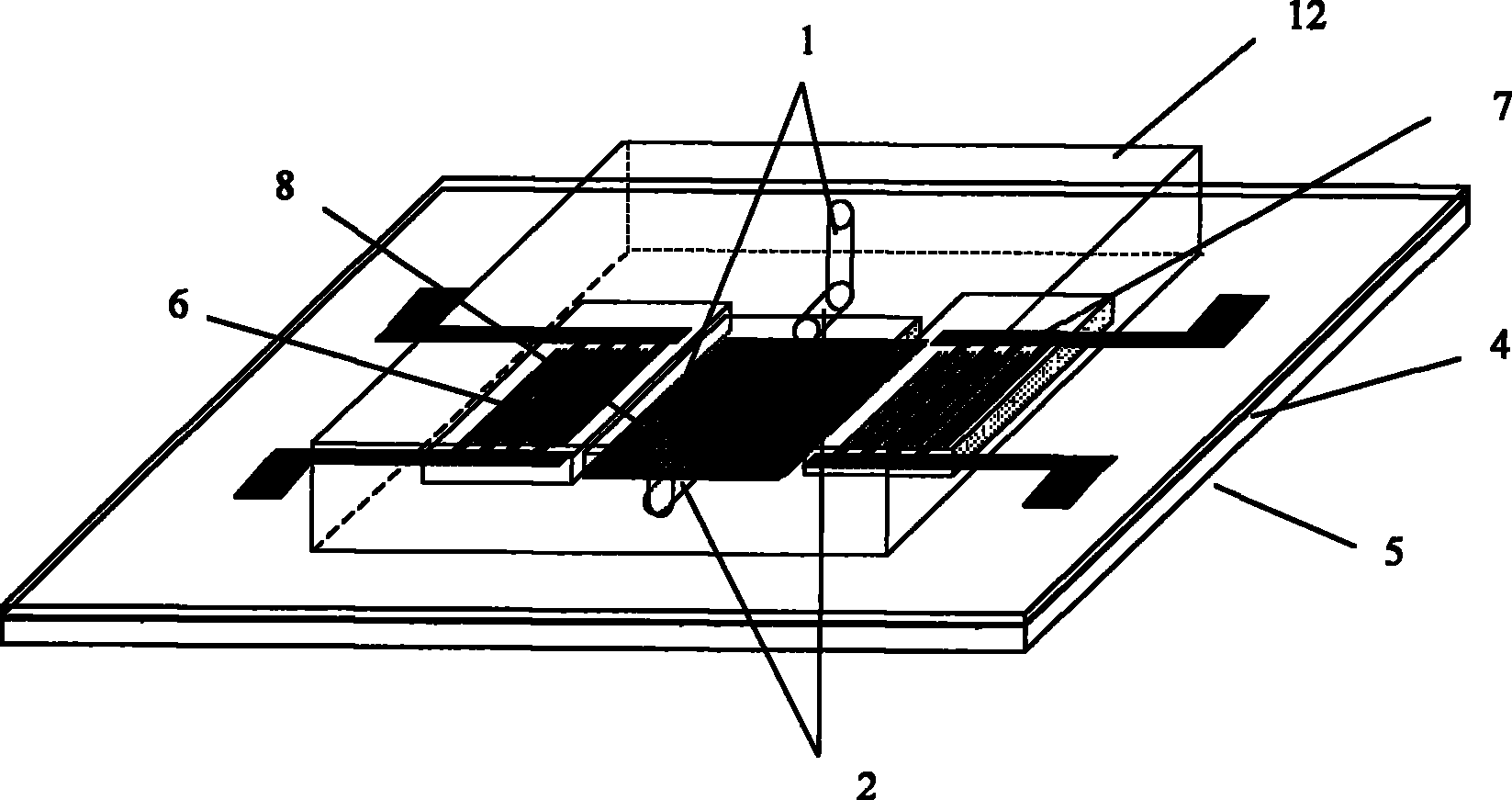
本发明提供的乐甫型声波(简称乐甫波)传感器的封装结构的装置,该结构包括乐甫波传感器,该乐甫波传感器从上至下包括:敏感膜3、波导层4、压电基片5,该压电基片5两端分别沉积有输入叉指换能器10、输出叉指换能器11,所述输入叉指换能器10和输出叉指换能器11位于敏感膜3的左、右两侧,其特征在于:还包括有微流体芯片12,该微流体芯片12对应地键合在乐甫波传感器上;The device of the packaging structure of the Love-type acoustic wave (abbreviated as Love-wave) sensor provided by the present invention, the structure comprises a Love-wave sensor, and the Love-wave sensor comprises from top to bottom: a
所述的微流体芯片12与乐甫波传感器的接触面上,对应于输入叉指换能器10、输出叉指换能器11、敏感膜3的区域的部分设置有凹槽,以和乐甫波传感器键合后形成互不连通的输入叉指换能器空腔6、输出叉指换能器空腔7和敏感膜空腔8;On the contact surface between the
所述的微流体芯片12与乐甫波传感器的接触部分的表面上、位于敏感膜3的上、下两侧还设置有若干微通道2,所述微通道2的一端连通敏感膜空腔8,另一端连通微流体芯片12上设置的用于待测物进、出入的通孔1。On the surface of the contact part of the
作为本发明的一种改进,所述的微流体芯片12采用刚性材料,由刚性有机聚合物材料和弹性材料制成,常用的有单晶硅、石英、玻璃、聚甲基丙烯酸甲酯(PMMA)和聚二甲基硅氧烷(PDMS)。As an improvement of the present invention, the
作为本发明的一种改进,所述输入叉指换能器10和输出叉指换能器11被波导层4覆盖或被暴露在波导层4之外。As an improvement of the present invention, the
作为本发明的另一种改进,所述的乐甫波传感器的敏感膜3铺设在空腔8的底部。As another improvement of the present invention, the
作为本发明的又一种改进,所述的微通道2采用分岔式结构,其连通通孔1的一端为一支微通道,微通道2连通敏感膜空腔8的另一端为均匀分布的多支微通道。以在敏感膜上均匀注入待测物。As another improvement of the present invention, the
作为本发明的再一种改进,所述的通孔1为两个或两个以上,分布于敏感膜3的上、下两侧。As another improvement of the present invention, there are two or more through
本发明的优点在于:本发明将微流体芯片键合在乐甫波传感器上,完成对乐甫波传感器的封装,所述的微流体芯片中的空腔6、7和8分别在叉指换能器10和11及敏感膜3区域上方,在空载和负载时互不连通,所述的微流体芯片中通孔1与微通道2连通,微通道2与敏感膜空腔8连通。The advantages of the present invention are: the present invention bonds the microfluidic chip on the Love wave sensor to complete the packaging of the Love wave sensor. Above the area of the
采用微流体芯片对乐甫波传感器进行封装,微流体芯片的结构在叉指换能器的上方留空,能有效保护乐甫波传感器的输入输出叉指换能器在工作时不受待测物影响,并且可精确控制待测物的进样、反应、分离,节约待测物的用量。相比现有技术,本发明的具有乐甫波传感器的封装结构的装置,可以降低传感器的损耗,精确控制待测物的进样、反应、分离和用量,提高传感器的重复性、准确性和可靠性。The Love wave sensor is packaged with a microfluidic chip. The structure of the microfluidic chip is left blank above the interdigital transducer, which can effectively protect the input and output interdigital transducers of the Love wave sensor from being tested during work. It can precisely control the sample injection, reaction, and separation of the analyte, and save the amount of the analyte. Compared with the prior art, the device with the packaging structure of the Love wave sensor of the present invention can reduce the loss of the sensor, precisely control the sample injection, reaction, separation and dosage of the analyte, and improve the repeatability, accuracy and accuracy of the sensor. reliability.
附图说明 Description of drawings
图1是本发明的具有乐甫波传感器的封装结构的装置的示意图;Fig. 1 is the schematic diagram of the device with the encapsulation structure of Love wave sensor of the present invention;
图2是本发明的具有乐甫波传感器的封装结构的装置的俯视图;Fig. 2 is the top view of the device with the encapsulation structure of Love wave sensor of the present invention;
图3是本发明的具有乐甫波传感器的封装结构的装置的实施例的剖视图;Fig. 3 is the sectional view of the embodiment of the device with the encapsulation structure of Love wave sensor of the present invention;
图4是本发明的具有乐甫波传感器的封装结构的装置的一实施例的结构主视图;Fig. 4 is the structural front view of an embodiment of the device with the packaging structure of the Love wave sensor of the present invention;
图5是本发明上述实施例中的叉指换能器的结构示意图。Fig. 5 is a schematic structural diagram of the interdigital transducer in the above embodiment of the present invention.
附图标识:Drawing logo:
1、通孔 2、微通道 3、敏感膜1. Through
4、波导层 5、基片 6、输入叉指换能器空腔4. Waveguide
7、输出叉指换能器空腔8、敏感膜空腔7. Output
10、输入叉指换能器 11、输出叉指换能器 12、微流体芯片10. Input IDT 11. Output IDT 12. Microfluidic chip
具体实施方式 Detailed ways
根据本发明的技术方案具体制作该结构,参见图1~3,由乐甫波传感器与微流体芯片两部分组成。According to the technical solution of the present invention, the structure is specifically manufactured, as shown in Figures 1 to 3, which consists of two parts, a Love wave sensor and a microfluidic chip.
乐甫波传感器结构,如图3所示,包括:压电基片5,覆盖波导层4、敏感膜3、输入叉指换能器10和输出叉指换能器11。本实施例中,乐甫波传感器压电基片采用St切割90度石英材料,厚度为0.5mm;输入、输出叉指换能器10、11均采用分裂指结构,如图5所示,其周期λ均为40微米,周期数为60,指条材料为铝,指条厚度为1500埃,指条宽度a和指间距b都为八分之一波长;孔径为2毫米;换能器中心频率f0=124MHz;波导层4采用二氧化硅材料,厚度为2μm;敏感膜3材料为金,厚度为50nm。The Love wave sensor structure, as shown in FIG. 3 , includes: a
微流体芯片12包括:与外部注射泵相连的通孔1和微通道2,输入、输出叉指换能器和敏感膜区域上方的空腔6、7和8。本实施例中,微流体芯片材料为聚二甲基硅氧烷(PDMS),整体大小为长12mm×宽18mm×高6mm,空腔6和7底面积为长2.8mm×宽3mm,高为25μm,空腔8底面积为长4.2mm×宽3mm,高为25um。注射泵采用了常用的手动注射器,通孔直径为500μm,微通道采用分岔式结构,如图4所示,每条通道宽度200μm,高度为25μm。微流体芯片采用等离子体键合的方式键合乐甫波传感器上。The
工作时通过手动注射器将待测物通过通孔1和微通道2注入到敏感膜区域的敏感膜空腔8中,待注满及充分反应后,记录加载待测物对乐甫波的影响,完成对待测物的测量。During work, the substance to be tested is injected into the
Claims (7)
Priority Applications (1)
| Application Number | Priority Date | Filing Date | Title |
|---|---|---|---|
| CN2008101015028A CN101527552B (en) | 2008-03-07 | 2008-03-07 | Device of packaging structure of love wave sensor |
Applications Claiming Priority (1)
| Application Number | Priority Date | Filing Date | Title |
|---|---|---|---|
| CN2008101015028A CN101527552B (en) | 2008-03-07 | 2008-03-07 | Device of packaging structure of love wave sensor |
Publications (2)
| Publication Number | Publication Date |
|---|---|
| CN101527552A CN101527552A (en) | 2009-09-09 |
| CN101527552B true CN101527552B (en) | 2011-12-07 |
Family
ID=41095279
Family Applications (1)
| Application Number | Title | Priority Date | Filing Date |
|---|---|---|---|
| CN2008101015028A Expired - Fee Related CN101527552B (en) | 2008-03-07 | 2008-03-07 | Device of packaging structure of love wave sensor |
Country Status (1)
| Country | Link |
|---|---|
| CN (1) | CN101527552B (en) |
Families Citing this family (12)
| Publication number | Priority date | Publication date | Assignee | Title |
|---|---|---|---|---|
| US9976192B2 (en) | 2006-03-10 | 2018-05-22 | Ldip, Llc | Waveguide-based detection system with scanning light source |
| US9528939B2 (en) | 2006-03-10 | 2016-12-27 | Indx Lifecare, Inc. | Waveguide-based optical scanning systems |
| CN102749130B (en) * | 2012-06-29 | 2014-11-05 | 长安大学 | Measuring device for LOVE-waveform ultramicro matter mass |
| US9440424B2 (en) * | 2014-05-05 | 2016-09-13 | Picosys Inc | Methods to form and to dismantle hermetically sealed chambers |
| WO2016019026A1 (en) * | 2014-07-29 | 2016-02-04 | Indx Lifecare, Inc. | Partially encapsulated waveguide based sensing chips, systems and methods of use |
| WO2016138427A1 (en) | 2015-02-27 | 2016-09-01 | Indx Lifecare, Inc. | Waveguide-based detection system with scanning light source |
| CN104768113B (en) * | 2015-03-20 | 2018-05-18 | 南京航空航天大学 | Love wave device structure for liquid multi-parameter sensing and detection method |
| CN107979352B (en) * | 2016-10-24 | 2021-07-06 | 天津大学 | Film bulk acoustic microfluidic mixing device |
| CN109239465B (en) * | 2018-10-11 | 2021-02-05 | 西南大学 | Microwave sensor based on substrate integrated waveguide and microfluidic technology |
| CN116068048B (en) * | 2021-10-29 | 2025-11-21 | 中国科学院声学研究所 | Love wave-based icing sensing device and love wave-based icing sensing system |
| CN116068047B (en) * | 2021-10-29 | 2026-03-24 | 中国科学院声学研究所 | A Lep-wave icing sensor with self-de-icing function and its preparation method |
| CN114865291B (en) | 2022-07-08 | 2022-12-02 | 荣耀终端有限公司 | Terminal antenna |
-
2008
- 2008-03-07 CN CN2008101015028A patent/CN101527552B/en not_active Expired - Fee Related
Also Published As
| Publication number | Publication date |
|---|---|
| CN101527552A (en) | 2009-09-09 |
Similar Documents
| Publication | Publication Date | Title |
|---|---|---|
| CN101527552B (en) | Device of packaging structure of love wave sensor | |
| KR100613398B1 (en) | Cantilever sensor type analysis system, manufacturing method and ultrafine material detection method using the same | |
| US8136403B2 (en) | Micromechanical sensor, sensor array and method | |
| TW201319563A (en) | Integrated IC wafer and plastic microfluidic substrate detection system | |
| JP5566543B2 (en) | Sensor, detection method, detection system, and detection apparatus | |
| Kato et al. | Wireless poly (dimethylsiloxane) quartz-crystal-microbalance biosensor chip fabricated by nanoimprint lithography for micropump integration aiming at application in lab-on-a-chip | |
| Kustanovich et al. | A high-performance lab-on-a-chip liquid sensor employing surface acoustic wave resonance | |
| US8968674B2 (en) | Fluid sensor preventing generation of air bubbles | |
| CN103917866B (en) | Elastic surface wave sensor | |
| JP4228993B2 (en) | Flow cell type QCM sensor | |
| JP7396984B2 (en) | Method and apparatus for interfacing a sensor with a fluid material | |
| CN105934667A (en) | Sensor device | |
| CN100348978C (en) | Polydimethylsiloxane based microorgan reagent analyzing and testing chip | |
| Papadakis et al. | Optimized acoustic biochip integrated with microfluidics for biomarkers detection in molecular diagnostics | |
| KR102238114B1 (en) | Using lithium niobate surface acoustic wave biosensor | |
| CN101639475B (en) | Device and method for realizing transmission of digital microfluid between two microfluidic chips | |
| WO2008019694A2 (en) | Bio surface acoustic wave (saw) resonator design for detection of a target analyte | |
| CN102419323A (en) | Device suitable for minim liquid mixed chemiluminescence reaction | |
| JP4567393B2 (en) | Microreactor and microreactor system | |
| US20160327575A1 (en) | Sensor | |
| TW202241587A (en) | Microfluidic biosensing chip integrating separate electrochemical electrodes | |
| CN100549689C (en) | Acoustic wave sensing device with integrated micro-channel, manufacturing method thereof and acoustic wave sensor | |
| Lange et al. | Packaging of surface acoustic wave (SAW) based biosensors: An important issue for future biomedical applications | |
| JP4228992B2 (en) | Flow cell type QCM sensor | |
| Mitsakakis et al. | An Integrated Microfluidics-on-SAW (“μF-on-SAW”) Setup for Multi-Sample Sensing |
Legal Events
| Date | Code | Title | Description |
|---|---|---|---|
| C06 | Publication | ||
| PB01 | Publication | ||
| C10 | Entry into substantive examination | ||
| SE01 | Entry into force of request for substantive examination | ||
| C14 | Grant of patent or utility model | ||
| GR01 | Patent grant | ||
| CF01 | Termination of patent right due to non-payment of annual fee |
Granted publication date: 20111207 Termination date: 20170307 |
|
| CF01 | Termination of patent right due to non-payment of annual fee |