CN1014936B - Bit-serial integrator circuitry - Google Patents
Bit-serial integrator circuitryInfo
- Publication number
- CN1014936B CN1014936B CN88106276A CN88106276A CN1014936B CN 1014936 B CN1014936 B CN 1014936B CN 88106276 A CN88106276 A CN 88106276A CN 88106276 A CN88106276 A CN 88106276A CN 1014936 B CN1014936 B CN 1014936B
- Authority
- CN
- China
- Prior art keywords
- serial
- bit
- input end
- signal
- coupled
- Prior art date
- Legal status (The legal status is an assumption and is not a legal conclusion. Google has not performed a legal analysis and makes no representation as to the accuracy of the status listed.)
- Expired
Links
Images
Classifications
-
- G—PHYSICS
- G06—COMPUTING; CALCULATING OR COUNTING
- G06F—ELECTRIC DIGITAL DATA PROCESSING
- G06F7/00—Methods or arrangements for processing data by operating upon the order or content of the data handled
- G06F7/38—Methods or arrangements for performing computations using exclusively denominational number representation, e.g. using binary, ternary, decimal representation
- G06F7/48—Methods or arrangements for performing computations using exclusively denominational number representation, e.g. using binary, ternary, decimal representation using non-contact-making devices, e.g. tube, solid state device; using unspecified devices
- G06F7/50—Adding; Subtracting
- G06F7/504—Adding; Subtracting in bit-serial fashion, i.e. having a single digit-handling circuit treating all denominations after each other
- G06F7/5045—Adding; Subtracting in bit-serial fashion, i.e. having a single digit-handling circuit treating all denominations after each other for multiple operands
-
- G—PHYSICS
- G06—COMPUTING; CALCULATING OR COUNTING
- G06F—ELECTRIC DIGITAL DATA PROCESSING
- G06F7/00—Methods or arrangements for processing data by operating upon the order or content of the data handled
- G06F7/38—Methods or arrangements for performing computations using exclusively denominational number representation, e.g. using binary, ternary, decimal representation
- G06F7/48—Methods or arrangements for performing computations using exclusively denominational number representation, e.g. using binary, ternary, decimal representation using non-contact-making devices, e.g. tube, solid state device; using unspecified devices
- G06F7/499—Denomination or exception handling, e.g. rounding or overflow
- G06F7/49942—Significance control
-
- G—PHYSICS
- G06—COMPUTING; CALCULATING OR COUNTING
- G06F—ELECTRIC DIGITAL DATA PROCESSING
- G06F7/00—Methods or arrangements for processing data by operating upon the order or content of the data handled
- G06F7/38—Methods or arrangements for performing computations using exclusively denominational number representation, e.g. using binary, ternary, decimal representation
- G06F7/48—Methods or arrangements for performing computations using exclusively denominational number representation, e.g. using binary, ternary, decimal representation using non-contact-making devices, e.g. tube, solid state device; using unspecified devices
- G06F7/499—Denomination or exception handling, e.g. rounding or overflow
- G06F7/49994—Sign extension
Landscapes
- Engineering & Computer Science (AREA)
- General Physics & Mathematics (AREA)
- Physics & Mathematics (AREA)
- Theoretical Computer Science (AREA)
- Mathematical Analysis (AREA)
- Pure & Applied Mathematics (AREA)
- Computational Mathematics (AREA)
- Computing Systems (AREA)
- Mathematical Optimization (AREA)
- General Engineering & Computer Science (AREA)
- Analogue/Digital Conversion (AREA)
- Compression, Expansion, Code Conversion, And Decoders (AREA)
- Dc Digital Transmission (AREA)
- Manipulation Of Pulses (AREA)
Abstract
A bit-serial integrator includes the cascade combination of a bit-serial adder, a first bit-serial register and a second bit-serial register. Input signal is applied to one input of the adder and the output terminal of the second bit-serial register is coupled to a second input of the adder. A transparent latch is coupled to an output of the first bit-serial register and is conditioned to pass a predetermined number of sample bits and then to latch and output a particular sample bit for the duration of a sample period. The output of the latch is an integrated, scaled and truncated representation of the input signal.
Description
The invention relates to a kind of circuit that integrating function is provided for gated clock bit serial system.
As you know, in digital circuit technique, carry out integration and can adopt delay element and adding circuit.The signal for the treatment of integration is added on the input end (addend) of adding circuit, and the output terminal of adding circuit is coupled on the input end of delay element, and the output terminal of delay element then is coupled on second input end (summand) of adding circuit.Integrated signal can be taken from the output terminal of adding circuit, also can take from the output terminal of delay element.This can referring to, for example, the 41st to 53 page of H.Urkowitz of " the radio engineer association Circuit theory journal " in one nine five seven year June is entitled as the article of " analysis of lag line periodic filter with synthetic ".
The value that sometimes often requires integrating circuit is provided is calibrated and is blocked.Block is in order to reduce the number of handled sample position, in order to reduce the processing circuitry scale or will the processing time to be reduced to the shortest.Lasting all and know, is to carry out in the integrating network if block, and promptly carries out between delay element and totalizer, then may produce undesirable consequence.It is inaccurate that these consequences show as handled signal, and some signal produces undesirable excessive increase, and may produce the vibration or the cycle limited.An object of the present invention is to provide a kind of minimum bit-serial integrator circuitry of hardware number of calibrating and blocking, can carry out integration and need usefulness with full position precision.
The present invention aims to provide a kind of bit-serial integrator circuitry with the signal combination device of R level shift register coupled in series that comprises.The output terminal of R level shift register is coupled to first joint of composite set by a N level shift register, treats that the signal of integration then is coupled on second input adapter of composite set.Each sampling period provides the gated clock source of R+N pulse at least to be coupled on each shift register, so that toward wherein transmitting the sample position.On the out splice going splice of R level shift register, can obtain through block, calibration and integration R position sample.
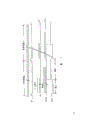
Fig. 1 is the block scheme of the bit-serial integrator circuitry of the embodiment of the invention.
Fig. 2 is to the useful oscillogram of explanation the present invention.
Fig. 3 includes the circuit block-diagram of the integration circuit of Fig. 1 in order to the DC component of elimination bit serial signal.
The present invention will be illustrated with regard to the situation of bit serial gated clock system.Pending sample is a R position two's complement bit serial sample.Referring to Fig. 2, each sample occurs with the synchronization of rate of the sample clock defined that is called SC.Various kinds one's own department or unit occurs synchronously with the time clock string that is called the clock signal of CLOCK R, and least significant bit (LSB) (LSB) occurs earlier in time, and highest significant position (MSB) or sign bit occur at last.The period ratio sampling period of the time clock string of CLOCK R is short.The pulse of timing signal CLOCK R is to be called the continuous system clock of CLOCK, waveform from one to produce.
Referring to Fig. 1.Integrating circuit comprises the totalizer 12 with first input end 10, treats that the sample of integration promptly is added on this first input end 10.The output terminal of totalizer 12 is coupled to signal and expands shift register (on the S * SR) 14, S * SR14 then comprises a R level serial shift register 16 and a transparent latch (TL) 18.Transparent latch 18 is controlled by two level controling signal XND, and when letter XND is in first state, various kinds one's own department or unit is intactly passed through, binary digit that will the transformation from first state to second state occurs simultaneously with signal XND latchs, and preserves and export this binary digit during signal XND is in second state.The output of transparent latch is the output of integrated signal through calibrating.The output terminal of serial register 16 is coupled on the N level serial shift register 22, and the output terminal of register 22 then is coupled on second input end of totalizer 12.Shift register 22 and 16 is by clock signal C LOCK(R+N) carry out timing, clock signal C LOCK(R+N with (R+N) in unit sampling period individual time clock string) and relation CLOCK(R) is as shown in Figure 2.
Control signal XND(is shown in Fig. 2) during R time clock from first state-transition to second state, thereby therefore R the sample position that register 16 is exported is latched, and repeats this R sample position in all the other times in existing sampling period.
Clock signal by, for example, producing the oscillator 23 of system clock, CLOCK and clock generator 24 produces.Clock generator 24 produces.Clock generator 24 produces CLOCK(R according to system clock), CLOCK(R+N) and signal such as XND, produce signal SC in case of necessity.These signals are to produce with general method in clock generator 24, its details does not belong to a part of the present invention, the personage who is familiar with the signal processing technology field is appreciated that timing relationship shown in Figure 2, thereby the circuit of above-mentioned clock generator 24 is not difficult to design.
Supposing has a series of R position two's complement bit serial sample to be added on the input adapter 10, R of each sample position or repeating during sign bit each sampling period after R-1 value binary digit occurring.The repetition of sign bit can be passed through, and for example, this transparent latch via suspension control signal XND control of various kinds is added on the joint 10 to be provided.Suppose that in addition the content of register 16 and 22 all gets null value, and 12 pairs of added signals of totalizer do not postpone to handle.During adding the sampling period of first sample, because register 16 and 22 content are got null value, thereby first sample is by constant in the totalizer 12, and at clock signal C LOCK(R+N) a R pulse after, reside in the shift register 16.During this period, output " OUT " is null value, and the content of promptly originally getting null value in the register 16 is by transparent latch 18.Latch 18 latched R carry-out bit and repeating it during the sampling period, thereby further made binary bit value that register 16 provided unlikely being placed on the terminal OUT between sampling period.
Register 16 is in another N clock period timing, and N LSB of sample is provided in the N level shift register 22.When the next sample period began, first sample just appeared on second input end of totalizer 12, and has a good reason can be added on the next added sample.In other words, reside in first sample in the register 22, its LSB and each binary digit thereafter can occur with corresponding binary digit simultaneously with the LSB that back (second) is added to the sample on the joint 10.
Because register 16 is a R level register and it with R+N pulse timing, thus first sample period (reaching each later sampling period) at the end, have only R MSB with numerical example to reside in the register 16.(annotate: although the input sample is a R scale-of-two bit wide, and numerical example can expand R+N scale-of-two bit wide to.) during afterwards each sampling period and R MSB of number provide via transparent latch 18 as output signal OUT.Export simultaneously with a R pulse of time clock string with R MSB of numerical example.That output sample is represented a significance bit position that N that totalizer 12 provides, blocks and is displaced to is lower and numerical example.To be displaced to the individual more low order position of N with numerical example is equivalent to and will be scaled to 2 with numerical example
-NDoubly.
But feed back to the sample of totalizer 12 both without blocking also without calibration via register 22.Therefore integration carries out with complete accurate way.
If the value of input sample is that A and numerical example are B, the sample that feeds back via register 22 is C, then can obtain the transport function of circuit by laxative remedy.Sample C equals to postpone the sample B in a sampling period, adopts general transform representation simultaneously
C=BZ
-1(1)
Then equal B=A+C (2) with numerical example B
Or B=A+BZ
-1(3)
With every perfect square journey (3) of laying equal stress on that pools together, then
B/A=A/(1-Z
-1) (4)
Equation (4) is to represent integral function with the transform representation.
If output sample OUT is D
D=2
-NBZ
-1(5)
And, then draw the D/A function and be in (4) substitution (5)
D/A=2
-NZ
-1/(1-Z
-1) (6)
This shows that output equals to postpone a sampling period and with the integration of 2 input signals of calibrating.
Under the layout type of Fig. 1, because the tandem compound of total total R+N shift register stage, thereby totalizer 12 is that provided can expand the bit wide of R+N to number.In addition if want with numerical example with 2
-XFeed back on the totalizer 12 under the situation of calibration, then the progression of register 22 can be reduced X, and between register 22 and totalizer 12, inserting transparent latch, this latch is a regulation in order to latch and to repeat in the sample position of (R+N-X) individual time clock.
Be that hypothesis totalizer 12 does not adopt processing delay in the layout type of Fig. 1.But, then sample B should be multiply by 2 if totalizer 12 adopts the processing delay of Y bit period
YSo transport function B/A has just become.
This factor part can reduce the Y level and compensate by the progression with register 22.At this moment, transport function B/A and D/A are:
B/A=2
Y/(1-Z
-1) (7)
And D/A=2
-(N-Y)/ (1-Z
-1) (8)
Not so if totalizer adopts the processing delay of Y bit period, then can increase Y by the umber of pulse that makes each time clock string and need not the transport function of equation (4) and (6) to be kept perfectly circuit component 16 and 22 other any changes of do.At this moment the clock signal that is added to register 16 and 22 can contain R+N+Y pulse in each string.
Secondly referring to Fig. 3.Each element supposition of numbering expression equally with each element of Fig. 1 among Fig. 3 is identical with this element of Fig. 1.Circuit among Fig. 3 can be in order to remove DC component from the bit serial signal of bit serial audio signal and so on.Suppose, for example, be added to signal on the terminal 32 and be no symbol normal binary signal, and all values all are positive from analog-digital converter.Transfer process normally is added to the direct current reference power source on the digitized signal.From, for example, the audio signal of broadcast source generally is an AC signal.If DC component is not removed, then require processing circuitry can handle dynamic range usually than exchanging the desired bigger signal of audio signal.Therefore for the number that will make whole signal Processing hardware is few as far as possible, total hope can be removed DC component.
The circuit of Fig. 3 comprises a bit serial two's complement subtract circuit 30 and an integrating circuit of introducing with reference to Fig. 1.Input signal (AIN) is coupled on the minuend input end of subtracter 30, and integrating circuit terminal OUT then is coupled on the subtrahend input end of subtracter.Be noted that in fact if signal AC
OUTBe to be coupled on the subtrahend input end of the subtracter that exchanges with totalizer 12, then in fact subtracter 30 and totalizer 12 can exchange.
Signal AC
OUTEqual signal AIN and deduct the difference that the output OUT from integrating circuit draws.From equation (6) as can be known, the signal OUT from integrating circuit is:
Compile every and the reformation transport function, then the AC of Fig. 3
OUT/ AIN can (11) formula represent:
AC
OUT/AIN=(Z-1)/(Z-1+2
-N) (11)
Concerning less than the relevant signals sampling cycle, this transport function contains zero under zero hertz, about 2
-NFs/2 π contains a limit for following hertz, and wherein fs is a sample frequency.Sound bandwidth is 20 hertz to 20 kilo hertzs.Supposing to satisfy the sampling period is 300 kilo hertzs less than the sample frequency of this standard of maximal audio cycle, then loses any audio signal scope for unlikely, the frequency of this limit should less than 20 hertz or
2
-Nfs/2π<20 (12)
N can satisfy this condition than 11 hours.It is at 11.6 hertz of places that N equals 12: 3 decibels of points, and N equals 13: 3 decibels of points and then reduces to 5.8 hertz.Exchange audio signal like this and can pass through in fact, without any loss, can eliminate DC component fully simultaneously on the amplitude.
Now hypothesis subtracter 30 and totalizer 12 each all sample of signal is adopted the delay of a bit period, then with respect to the sample data of being set up in a certain gated clock system, a bit period postpones to be equivalent to be multiplied by a coefficient 2.So the output of subtracter 30 becomes
AC
OUT=2(AIN-OUT) (13)
According to equation (8), signal OUT becomes:

In (14) substitution (13), collection item and transposition, then transport function can be represented with (15) formula:
AC
OUT/AIN=2(Z-1)/(Z-1+2
-(N-2)) (15)
Here have one zero again at zero hertz place, but at this moment limit is 2
-(N-2)The conspicuous place of fs/2 π, and amplitude increases by 1 times.Will with on set up limit under the identical frequency of example, N should increase by 2.
" time clock string " speech has been described in detail in detail in the following claims." time clock string " can occupy the whole sampling period, also can only occupy the part less than the whole sampling period, and this depends on selected specific circuit elements, i.e. register progression and sampling period and decide.If the time clock string occupies the whole sampling period, then clock signal can occur as the consecutive pulses string, and promptly the time clock string can not see that tangible separation is arranged one by one each other immediately following adjoining.Employed in claims " time clock string " speech also comprises this contingent situation.
Claims (4)
1, a kind of contraposition serial signal carries out the bit-serial integrator circuitry that integration is used, and this circuit comprises:
One signal input terminal (1N) is in order to apply the bit serial signal;
One composite set (12), in order to mixing the bit serial signal, this device has first input end, one second input end and an output terminal that is coupled to described signal input part;
One first serial shift register (16) has R level (R is an integer), also has input end, an output terminal and a clock input end that is coupled on the described composite set (12); This circuit is characterised in that:
Second serial shift register (22) has N level (N is an integer), and is coupled to an output terminal and a clock input end on second input end that input end, on the output terminal of described serial shift register (16) is coupled to described composite set;
Be used to apply the device (23 of time clock string, 24), in order to time clock is serially added on described first serial register (16) and second serial register (22), the binary digit that pulse in the described time clock string and described bit serial signal occur is synchronous, and the per sampling period of umber of pulse in the described time clock string is at least R+N; With
Transparent latch means (18), be coupled on the output terminal of described first serial shift register (16), in order to during first predetermined portions of described time clock string, the sample binary digit being passed through, and latch and export predetermined sample binary digit during each sampling period after described predetermined portions.
2, as bit-serial integrator circuitry that claim 1 proposed, it is characterized in that, described time clock string bringing device (23,24) provides number to equal a train of impulses of delay period integer between the lead-out terminal of the input end of described composite set (12) and described second serial shift register (22).
3, as bit-serial integrator circuitry that claim 2 proposed, it is characterized in that, described composite set (12) has the processing delay of a sample bit period between its input end and output terminal, and described time clock string bringing device provides quantity to equal the train of impulses of R+N+1.
4, the bit-serial integrator circuitry that claim 3 proposed is characterized in that comprising:
Another serial combination device (30), having one is coupled on the first input end that first input end, on the output terminal of the transparent latch means of described bit serial (18) is coupled to described composite set (12) and output terminal and one second input end of the signal of handling is arranged on it; With
Bit serial signal bringing device (AIN) is in order to be added to the bit serial signal on second input end of described another bit serial composite set (30).
Applications Claiming Priority (2)
| Application Number | Priority Date | Filing Date | Title |
|---|---|---|---|
| US088,340 | 1987-08-24 | ||
| US07/088,340 US4841466A (en) | 1987-08-24 | 1987-08-24 | Bit-serial integrator circuitry |
Publications (2)
| Publication Number | Publication Date |
|---|---|
| CN1031768A CN1031768A (en) | 1989-03-15 |
| CN1014936B true CN1014936B (en) | 1991-11-27 |
Family
ID=22210796
Family Applications (1)
| Application Number | Title | Priority Date | Filing Date |
|---|---|---|---|
| CN88106276A Expired CN1014936B (en) | 1987-08-24 | 1988-08-24 | Bit-serial integrator circuitry |
Country Status (8)
| Country | Link |
|---|---|
| US (1) | US4841466A (en) |
| EP (1) | EP0304841B1 (en) |
| JP (1) | JPS6470828A (en) |
| KR (1) | KR0128505B1 (en) |
| CN (1) | CN1014936B (en) |
| CA (1) | CA1290458C (en) |
| DE (1) | DE3853655T2 (en) |
| FI (1) | FI93284C (en) |
Cited By (1)
| Publication number | Priority date | Publication date | Assignee | Title |
|---|---|---|---|---|
| TWI426397B (en) * | 2009-06-29 | 2014-02-11 | Lee Ming Inst Technology | Can be used in a signal interval in the unequal spacing of the sample, the signal in this interval between a single and multiple numerical integration device. |
Families Citing this family (7)
| Publication number | Priority date | Publication date | Assignee | Title |
|---|---|---|---|---|
| US5313469A (en) * | 1993-06-11 | 1994-05-17 | Northern Telecom Limited | Self-testable digital integrator |
| EP1001567A1 (en) | 1998-11-13 | 2000-05-17 | TELEFONAKTIEBOLAGET LM ERICSSON (publ) | Combiner |
| EP1011281A3 (en) | 1998-12-18 | 2000-07-05 | TELEFONAKTIEBOLAGET L M ERICSSON (publ) | Flexible CDMA combiner |
| WO2007042850A1 (en) | 2005-10-12 | 2007-04-19 | Acco | Insulated gate field-effet transistor having a dummy gate |
| TWI444021B (en) * | 2007-09-17 | 2014-07-01 | Htc Corp | Method for decrypting serial transmission signal |
| US7808415B1 (en) * | 2009-03-25 | 2010-10-05 | Acco Semiconductor, Inc. | Sigma-delta modulator including truncation and applications thereof |
| US8532584B2 (en) | 2010-04-30 | 2013-09-10 | Acco Semiconductor, Inc. | RF switches |
Family Cites Families (6)
| Publication number | Priority date | Publication date | Assignee | Title |
|---|---|---|---|---|
| US3757261A (en) * | 1972-02-11 | 1973-09-04 | Collins Radio Co | Integration and filtration circuit apparatus |
| US3919535A (en) * | 1974-08-21 | 1975-11-11 | Singer Co | Multiple addend adder and multiplier |
| US4023019A (en) * | 1974-09-23 | 1977-05-10 | The United States Of America As Represented By The Secretary Of The Navy | Automatic scaled digital integrator |
| SU739566A1 (en) * | 1978-01-04 | 1980-06-05 | Предприятие П/Я А-3890 | Digital integrator |
| US4246642A (en) * | 1979-01-22 | 1981-01-20 | Ricoh Company, Ltd. | Leaky digital integrator |
| JPH105347A (en) * | 1996-06-21 | 1998-01-13 | Toyo Sangyo Kk | Low frequency therapy equipment |
-
1987
- 1987-08-24 US US07/088,340 patent/US4841466A/en not_active Expired - Lifetime
-
1988
- 1988-07-26 CA CA000573061A patent/CA1290458C/en not_active Expired - Fee Related
- 1988-08-17 FI FI883816A patent/FI93284C/en not_active IP Right Cessation
- 1988-08-22 DE DE3853655T patent/DE3853655T2/en not_active Expired - Fee Related
- 1988-08-22 EP EP88113616A patent/EP0304841B1/en not_active Expired - Lifetime
- 1988-08-23 KR KR1019880010680A patent/KR0128505B1/en not_active IP Right Cessation
- 1988-08-23 JP JP63207497A patent/JPS6470828A/en active Granted
- 1988-08-24 CN CN88106276A patent/CN1014936B/en not_active Expired
Cited By (1)
| Publication number | Priority date | Publication date | Assignee | Title |
|---|---|---|---|---|
| TWI426397B (en) * | 2009-06-29 | 2014-02-11 | Lee Ming Inst Technology | Can be used in a signal interval in the unequal spacing of the sample, the signal in this interval between a single and multiple numerical integration device. |
Also Published As
| Publication number | Publication date |
|---|---|
| CN1031768A (en) | 1989-03-15 |
| FI883816A (en) | 1989-02-25 |
| FI93284C (en) | 1995-03-10 |
| JPH0421218B2 (en) | 1992-04-09 |
| EP0304841B1 (en) | 1995-04-26 |
| CA1290458C (en) | 1991-10-08 |
| US4841466A (en) | 1989-06-20 |
| DE3853655D1 (en) | 1995-06-01 |
| FI883816A0 (en) | 1988-08-17 |
| EP0304841A3 (en) | 1991-03-20 |
| FI93284B (en) | 1994-11-30 |
| JPS6470828A (en) | 1989-03-16 |
| KR0128505B1 (en) | 1998-04-15 |
| DE3853655T2 (en) | 1995-10-19 |
| KR890004233A (en) | 1989-04-20 |
| EP0304841A2 (en) | 1989-03-01 |
Similar Documents
| Publication | Publication Date | Title |
|---|---|---|
| US5382955A (en) | Error tolerant thermometer-to-binary encoder | |
| CN1015307B (en) | Sigma-delta modulator for d-to-a converter | |
| ES8606713A1 (en) | Method and apparatus for uniformly encoding data occurring with different word lengths | |
| CN86101813A (en) | Have block deviation compensation numeral surely than circuit | |
| US4750167A (en) | Digital audio transmission system | |
| CN1014936B (en) | Bit-serial integrator circuitry | |
| US5181184A (en) | Apparatus for multiplying real-time 2's complement code in a digital signal processing system and a method for the same | |
| US4352129A (en) | Digital recording apparatus | |
| KR920009642B1 (en) | Data condensing circuit | |
| KR930002136B1 (en) | Method of transmitting information, encoding device for use in the method, and decoding device for use in the method | |
| CN1771665A (en) | Bi-quad digital filter configured with a bit binary rate multiplier | |
| CN86105230A (en) | Interpolator/decimator filter construction and notch filter thereof | |
| US4189715A (en) | μ-Law to floating point converter | |
| US4040049A (en) | Tandem block digital processor for use with nonuniformly encoded digital data | |
| US5107265A (en) | Analog to digital converter | |
| EP0090314A2 (en) | PCM encoder conformable to the A-law | |
| US4860241A (en) | Method and apparatus for cellular division | |
| GB2175167A (en) | Digital filters | |
| JP2917095B2 (en) | Thermometer code processing method and apparatus | |
| GB2157032A (en) | Digital parallel odder | |
| JP3071607B2 (en) | Multiplication circuit | |
| CN86107844A (en) | A kind of realization of digital filter | |
| RU1815797C (en) | Digital filter | |
| KR880001011B1 (en) | Digital signal process method | |
| CA1127307A (en) | .mu.-LAW TO FLOATING POINT CONVERTER |
Legal Events
| Date | Code | Title | Description |
|---|---|---|---|
| C06 | Publication | ||
| PB01 | Publication | ||
| C10 | Entry into substantive examination | ||
| SE01 | Entry into force of request for substantive examination | ||
| C13 | Decision | ||
| GR02 | Examined patent application | ||
| C14 | Grant of patent or utility model | ||
| GR01 | Patent grant | ||
| C15 | Extension of patent right duration from 15 to 20 years for appl. with date before 31.12.1992 and still valid on 11.12.2001 (patent law change 1993) | ||
| OR01 | Other related matters | ||
| C19 | Lapse of patent right due to non-payment of the annual fee | ||
| CF01 | Termination of patent right due to non-payment of annual fee |