CN101281334A - Display substrate and LCD with the same - Google Patents
Display substrate and LCD with the same Download PDFInfo
- Publication number
- CN101281334A CN101281334A CNA2008100805838A CN200810080583A CN101281334A CN 101281334 A CN101281334 A CN 101281334A CN A2008100805838 A CNA2008100805838 A CN A2008100805838A CN 200810080583 A CN200810080583 A CN 200810080583A CN 101281334 A CN101281334 A CN 101281334A
- Authority
- CN
- China
- Prior art keywords
- data line
- pixel
- line
- voltage
- gate
- Prior art date
- Legal status (The legal status is an assumption and is not a legal conclusion. Google has not performed a legal analysis and makes no representation as to the accuracy of the status listed.)
- Pending
Links
Images


Classifications
-
- G—PHYSICS
- G09—EDUCATION; CRYPTOGRAPHY; DISPLAY; ADVERTISING; SEALS
- G09G—ARRANGEMENTS OR CIRCUITS FOR CONTROL OF INDICATING DEVICES USING STATIC MEANS TO PRESENT VARIABLE INFORMATION
- G09G3/00—Control arrangements or circuits, of interest only in connection with visual indicators other than cathode-ray tubes
- G09G3/20—Control arrangements or circuits, of interest only in connection with visual indicators other than cathode-ray tubes for presentation of an assembly of a number of characters, e.g. a page, by composing the assembly by combination of individual elements arranged in a matrix no fixed position being assigned to or needed to be assigned to the individual characters or partial characters
- G09G3/34—Control arrangements or circuits, of interest only in connection with visual indicators other than cathode-ray tubes for presentation of an assembly of a number of characters, e.g. a page, by composing the assembly by combination of individual elements arranged in a matrix no fixed position being assigned to or needed to be assigned to the individual characters or partial characters by control of light from an independent source
- G09G3/36—Control arrangements or circuits, of interest only in connection with visual indicators other than cathode-ray tubes for presentation of an assembly of a number of characters, e.g. a page, by composing the assembly by combination of individual elements arranged in a matrix no fixed position being assigned to or needed to be assigned to the individual characters or partial characters by control of light from an independent source using liquid crystals
- G09G3/3611—Control of matrices with row and column drivers
- G09G3/3614—Control of polarity reversal in general
-
- G—PHYSICS
- G02—OPTICS
- G02F—OPTICAL DEVICES OR ARRANGEMENTS FOR THE CONTROL OF LIGHT BY MODIFICATION OF THE OPTICAL PROPERTIES OF THE MEDIA OF THE ELEMENTS INVOLVED THEREIN; NON-LINEAR OPTICS; FREQUENCY-CHANGING OF LIGHT; OPTICAL LOGIC ELEMENTS; OPTICAL ANALOGUE/DIGITAL CONVERTERS
- G02F1/00—Devices or arrangements for the control of the intensity, colour, phase, polarisation or direction of light arriving from an independent light source, e.g. switching, gating or modulating; Non-linear optics
- G02F1/01—Devices or arrangements for the control of the intensity, colour, phase, polarisation or direction of light arriving from an independent light source, e.g. switching, gating or modulating; Non-linear optics for the control of the intensity, phase, polarisation or colour
- G02F1/13—Devices or arrangements for the control of the intensity, colour, phase, polarisation or direction of light arriving from an independent light source, e.g. switching, gating or modulating; Non-linear optics for the control of the intensity, phase, polarisation or colour based on liquid crystals, e.g. single liquid crystal display cells
- G02F1/133—Constructional arrangements; Operation of liquid crystal cells; Circuit arrangements
- G02F1/1333—Constructional arrangements; Manufacturing methods
- G02F1/1335—Structural association of cells with optical devices, e.g. polarisers or reflectors
- G02F1/133553—Reflecting elements
- G02F1/133555—Transflectors
-
- G—PHYSICS
- G02—OPTICS
- G02F—OPTICAL DEVICES OR ARRANGEMENTS FOR THE CONTROL OF LIGHT BY MODIFICATION OF THE OPTICAL PROPERTIES OF THE MEDIA OF THE ELEMENTS INVOLVED THEREIN; NON-LINEAR OPTICS; FREQUENCY-CHANGING OF LIGHT; OPTICAL LOGIC ELEMENTS; OPTICAL ANALOGUE/DIGITAL CONVERTERS
- G02F1/00—Devices or arrangements for the control of the intensity, colour, phase, polarisation or direction of light arriving from an independent light source, e.g. switching, gating or modulating; Non-linear optics
- G02F1/01—Devices or arrangements for the control of the intensity, colour, phase, polarisation or direction of light arriving from an independent light source, e.g. switching, gating or modulating; Non-linear optics for the control of the intensity, phase, polarisation or colour
- G02F1/13—Devices or arrangements for the control of the intensity, colour, phase, polarisation or direction of light arriving from an independent light source, e.g. switching, gating or modulating; Non-linear optics for the control of the intensity, phase, polarisation or colour based on liquid crystals, e.g. single liquid crystal display cells
- G02F1/133—Constructional arrangements; Operation of liquid crystal cells; Circuit arrangements
- G02F1/136—Liquid crystal cells structurally associated with a semi-conducting layer or substrate, e.g. cells forming part of an integrated circuit
- G02F1/1362—Active matrix addressed cells
- G02F1/136286—Wiring, e.g. gate line, drain line
-
- G—PHYSICS
- G09—EDUCATION; CRYPTOGRAPHY; DISPLAY; ADVERTISING; SEALS
- G09G—ARRANGEMENTS OR CIRCUITS FOR CONTROL OF INDICATING DEVICES USING STATIC MEANS TO PRESENT VARIABLE INFORMATION
- G09G3/00—Control arrangements or circuits, of interest only in connection with visual indicators other than cathode-ray tubes
- G09G3/20—Control arrangements or circuits, of interest only in connection with visual indicators other than cathode-ray tubes for presentation of an assembly of a number of characters, e.g. a page, by composing the assembly by combination of individual elements arranged in a matrix no fixed position being assigned to or needed to be assigned to the individual characters or partial characters
- G09G3/34—Control arrangements or circuits, of interest only in connection with visual indicators other than cathode-ray tubes for presentation of an assembly of a number of characters, e.g. a page, by composing the assembly by combination of individual elements arranged in a matrix no fixed position being assigned to or needed to be assigned to the individual characters or partial characters by control of light from an independent source
- G09G3/36—Control arrangements or circuits, of interest only in connection with visual indicators other than cathode-ray tubes for presentation of an assembly of a number of characters, e.g. a page, by composing the assembly by combination of individual elements arranged in a matrix no fixed position being assigned to or needed to be assigned to the individual characters or partial characters by control of light from an independent source using liquid crystals
- G09G3/3611—Control of matrices with row and column drivers
- G09G3/3648—Control of matrices with row and column drivers using an active matrix
-
- G—PHYSICS
- G02—OPTICS
- G02F—OPTICAL DEVICES OR ARRANGEMENTS FOR THE CONTROL OF LIGHT BY MODIFICATION OF THE OPTICAL PROPERTIES OF THE MEDIA OF THE ELEMENTS INVOLVED THEREIN; NON-LINEAR OPTICS; FREQUENCY-CHANGING OF LIGHT; OPTICAL LOGIC ELEMENTS; OPTICAL ANALOGUE/DIGITAL CONVERTERS
- G02F1/00—Devices or arrangements for the control of the intensity, colour, phase, polarisation or direction of light arriving from an independent light source, e.g. switching, gating or modulating; Non-linear optics
- G02F1/01—Devices or arrangements for the control of the intensity, colour, phase, polarisation or direction of light arriving from an independent light source, e.g. switching, gating or modulating; Non-linear optics for the control of the intensity, phase, polarisation or colour
- G02F1/13—Devices or arrangements for the control of the intensity, colour, phase, polarisation or direction of light arriving from an independent light source, e.g. switching, gating or modulating; Non-linear optics for the control of the intensity, phase, polarisation or colour based on liquid crystals, e.g. single liquid crystal display cells
- G02F1/133—Constructional arrangements; Operation of liquid crystal cells; Circuit arrangements
- G02F1/136—Liquid crystal cells structurally associated with a semi-conducting layer or substrate, e.g. cells forming part of an integrated circuit
- G02F1/1362—Active matrix addressed cells
- G02F1/13624—Active matrix addressed cells having more than one switching element per pixel
-
- G—PHYSICS
- G09—EDUCATION; CRYPTOGRAPHY; DISPLAY; ADVERTISING; SEALS
- G09G—ARRANGEMENTS OR CIRCUITS FOR CONTROL OF INDICATING DEVICES USING STATIC MEANS TO PRESENT VARIABLE INFORMATION
- G09G2300/00—Aspects of the constitution of display devices
- G09G2300/08—Active matrix structure, i.e. with use of active elements, inclusive of non-linear two terminal elements, in the pixels together with light emitting or modulating elements
- G09G2300/0809—Several active elements per pixel in active matrix panels
- G09G2300/0823—Several active elements per pixel in active matrix panels used to establish symmetry in driving, e.g. with polarity inversion
-
- G—PHYSICS
- G09—EDUCATION; CRYPTOGRAPHY; DISPLAY; ADVERTISING; SEALS
- G09G—ARRANGEMENTS OR CIRCUITS FOR CONTROL OF INDICATING DEVICES USING STATIC MEANS TO PRESENT VARIABLE INFORMATION
- G09G2330/00—Aspects of power supply; Aspects of display protection and defect management
- G09G2330/02—Details of power systems and of start or stop of display operation
- G09G2330/021—Power management, e.g. power saving
Abstract
The present invention provides a display substrate and liquid crystal display having the same. The liquid crystal display includes: a first pixel connected to first and second gate lines, a first positive data line and a first negative data line, and which is supplied with a positive data voltage from the first positive data line when enabled by a first gate-on voltage from the first gate line, and is supplied with a negative data voltage from the first negative data line when enabled by a second gate-on voltage from the second gate line; and a second pixel connected to the first and second gate lines, a second positive data line and a second negative data line, and which is supplied with a negative data voltage from the second negative data line when enabled by the first gate-on voltage and is supplied with a positive data voltage from the second positive data line when enabled by the second gate-on voltage.
Description
Technical field
The present invention relates to a kind of substrate and a kind of LCD of showing, more particularly, relate to demonstration substrate and a kind of LCD that a kind of power consumption reduces with this demonstration substrate with this demonstration substrate.
Background technology
LCD comprises first substrate with a plurality of pixel electrodes, second substrate with common electrode, has the liquid crystal layer of dielectric anisotropy between first substrate and second substrate, drives the gate drivers of many gate lines and the data driver of outputting data signals.
In order to prevent the deterioration of liquid crystal layer, LCD is utilized the reversal of poles driving method.For example, various reversal of poles driving methods comprise frame inversion driving, row inversion driving, row inversion driving and some inversion driving.In the frame inversion driving method, the polarity of data voltage of all pixel electrodes that is applied to a plurality of pixel electrodes is identical in designated frame.Be expert in the inversion driving method, the polarity of data voltage that is applied to the pixel electrode in the nominated bank of designated frame is identical.In the row inversion driving method, the polarity of data voltage that is applied to the pixel electrode in the specify columns of designated frame is identical.In an inversion driving method, the polarity that is applied to corresponding adjacent pixel electrodes is opposite each other in designated frame.
In the above in every kind of reversal of poles driving method of Miao Shuing, in designated frame, will the data voltage of positive polarity be arranged and have the data voltage of negative polarity to be applied to corresponding pixel electrode, in frame subsequently, make the corresponding alternating polarity ground counter-rotating of the data voltage that is applied to pixel electrode with respect to the common-battery pressing element with respect to the common-battery pressing element.
Therefore, drive in order to carry out reversal of poles, data driver will have the data voltage of positive polarity alternately and negative polarity sequentially to be applied to the data line of LCD with respect to the common-battery pressing element.
Yet, increased the power consumption of LCD at the voltage blocked operation that utilizes the wide data voltage of variation range to carry out carrying out in the process that reversal of poles drives.
Summary of the invention
The invention provides a kind of demonstration substrate and a kind of LCD (LCD) that comprises this demonstration substrate that reduces its power consumption effectively.
According to exemplary embodiment of the present invention, a kind of LCD comprises: the first correction data line and the second correction data line, every supply positive polarity data voltage in the first correction data line and the second correction data line; The first negative data line and the second negative data line, every supply negative polarity data voltage in the first negative data line and the second negative data line; First pixel, be connected to first grid polar curve and second grid line, wherein, when making the work of first pixel by first grid forward voltage from first grid polar curve, first pixel is supplied the positive polarity data voltage from the first correction data line, when making the work of first pixel by the second grid forward voltage from the second grid line, first pixel is supplied the negative polarity data voltage from the first negative data line; Second pixel, be connected to first grid polar curve and second grid line, wherein, when making the work of second pixel by first grid forward voltage from first grid polar curve, second pixel is supplied the negative polarity data voltage from the second negative data line, when making the work of second pixel by the second grid forward voltage from the second grid line, second pixel is supplied the positive polarity data voltage from the second correction data line.
In the different frame in a plurality of frames of LCD, all provide first grid forward voltage and second grid forward voltage.
The current potential that the current potential of positive polarity data voltage is pressed with respect to the direct current common-battery is for just.In addition, the current potential of negative polarity data voltage is negative with respect to the current potential of direct current common-battery pressure.
First pixel and second pixel include: first on-off element, work by the first grid forward voltage; The second switch element is worked by the second grid forward voltage; Pixel electrode is connected to first on-off element and second switch element, wherein, applies positive polarity data voltage or negative polarity data voltage by first on-off element or second switch element to pixel electrode.
In selectable exemplary embodiment, first pixel and second pixel include: first on-off element, work by the first grid forward voltage; The second switch element is worked by the second grid forward voltage; Pixel electrode is connected to first on-off element and second switch element, wherein, applies positive polarity data voltage or negative polarity data voltage by first on-off element or second switch element to pixel electrode; Common electrode, and pixel-oriented electrode relative with pixel electrode, and be applied in direct current common-battery pressure; Liquid crystal layer places between pixel electrode and the common electrode; Reflectance coating is arranged between pixel electrode and the liquid crystal layer.
At least a portion of in reflectance coating and first grid polar curve and the second grid line at least one is stacked.
LCD also can comprise: substrate, and wherein, first grid polar curve and second grid line are formed in the described substrate; The light blocking pattern is formed in the substrate between the adjacent pixel electrodes.At least a portion of light blocking pattern and the first correction data line or the first negative data line are stacked, and stacked with the second correction data line or the second negative data line.
LCD also can comprise the black matrix that is arranged on the common electrode, and wherein, at least a portion of black matrix and the first correction data line or the first negative data line are stacked, and stacked with the second correction data line or the second negative data line.
In the exemplary embodiment, when from the first correction data line supply positive polarity data voltage, the first negative data line is floated.In addition, when from the first negative data line supply negative polarity data voltage, the first correction data line is floated.
LCD also can comprise data driver and a plurality of transmission gate.
Data driver provides the positive polarity data voltage according to picture signal to the first correction data line and the second correction data line, perhaps provides the negative polarity data voltage to the first negative data line and the second negative data line.
When providing the positive polarity data voltage from data driver, a plurality of transmission gates provide the positive polarity data voltage to the first correction data line and the second correction data line; When providing the negative polarity data voltage from data driver, a plurality of transmission gates provide the negative polarity data voltage to the first negative data line and the second negative data line.
In another exemplary embodiment, LCD also can comprise: the 3rd gate line and the 4th gate line; The 3rd pixel, be connected to the 3rd gate line, the 4th gate line, the first correction data line and the first negative data line, wherein, when making the work of the 3rd pixel by the 3rd gate-on voltage from the 3rd gate line, the 3rd pixel is supplied the positive polarity data voltage from the first correction data line, when making the work of the 3rd pixel by the 4th gate-on voltage from the 4th gate line, the 3rd pixel is supplied the negative polarity data voltage from the first negative data line; The 4th pixel, be connected to the 3rd gate line, the 4th gate line, the second correction data line and the second negative data line, wherein, when making the work of the 4th pixel by the 3rd gate-on voltage from the 3rd gate line, the 4th pixel is supplied the negative polarity data voltage from the second negative data line, when making the work of the 4th pixel by the 4th gate-on voltage from the 4th gate line, the 4th pixel is supplied the positive polarity data voltage from the second correction data line.
In another exemplary embodiment, LCD also can comprise: the 3rd gate line and the 4th gate line; The 3rd pixel, be connected to the 3rd gate line, the 4th gate line, the first correction data line and the first negative data line, wherein, when making the work of the 3rd pixel by the 3rd gate-on voltage from the 3rd gate line, the 3rd pixel is supplied the negative polarity data voltage from the first negative data line, when making the work of the 3rd pixel by the 4th gate-on voltage from the 4th gate line, the 3rd pixel is supplied the positive polarity data voltage from the first correction data line; The 4th pixel, be connected to the 3rd gate line, the 4th gate line, the second correction data line and the second negative data line, wherein, when making the work of the 4th pixel by the 3rd gate-on voltage from the 3rd gate line, the 4th pixel is supplied the positive polarity data voltage from the second correction data line, when making the work of the 4th pixel by the 4th gate-on voltage from the 4th gate line, the 4th pixel is supplied the negative polarity data voltage from the second negative data line.
According to another exemplary embodiment of the present invention, a kind of demonstration substrate comprises: dielectric base; First grid polar curve and second grid line; First data line and second data line are formed on the dielectric base, and all intersect with first grid polar curve and second grid line; The first film transistor is connected to the first grid polar curve and first data line, and comprises first drain electrode; Second thin film transistor (TFT) is connected to the second grid line and second data line, and comprises second drain electrode; First pixel electrode is connected to first drain electrode and second drain electrode; Reflectance coating.At least a portion of at least a portion of reflectance coating and first pixel electrode is stacked.
Reflectance coating also can be stacked with at least a portion of one of first grid polar curve and second grid line.
First pixel electrode is arranged between first data line and second data line.
Show that substrate also can comprise the light blocking pattern that is formed on the dielectric base, wherein, at least a portion of one of at least a portion of light blocking pattern and first data line and second data line is stacked.
When first data line applies data voltage, second data line is floated.
Show that substrate also can comprise: the 3rd data line and the 4th data line; The 3rd thin film transistor (TFT) is connected to first grid polar curve and the 3rd data line, and has the 3rd drain electrode; The 4th thin film transistor (TFT) is connected to second grid line and the 4th data line, and has the 4th drain electrode; Second pixel electrode is connected to the 3rd drain electrode and the 4th drain electrode.
Second pixel electrode is arranged between the 3rd data line and the 4th data line.
Show that substrate also can comprise the light blocking pattern, described light blocking pattern is formed on the dielectric base that is arranged between first pixel electrode and second pixel electrode, wherein, at least a portion of one of one of at least a portion of light blocking pattern and first data line and second data line and the 3rd data line and the 4th data line is stacked.
Description of drawings
By the reference accompanying drawing exemplary embodiment of the present invention is described in more detail, above-mentioned and others of the present invention, feature and advantage will become easier to be understood, in the accompanying drawings:
Fig. 1 is the block diagram of LCD (LCD) according to an exemplary embodiment of the present invention;
Fig. 2 A shows the signal timing diagram of the signal of the output of gate drivers according to an exemplary embodiment of the present invention from Fig. 1;
Fig. 2 B to Fig. 2 E shows the schematic circuit of the operation of the LCD according to an exemplary embodiment of the present invention among Fig. 1;
Fig. 3 A and Fig. 3 B show the schematic circuit of the operation of the LCD of another exemplary embodiment according to the present invention;
Fig. 4 A shows from the signal timing diagram of the signal of the gate drivers output of the LCD of the another exemplary embodiment according to the present invention;
Fig. 4 B and Fig. 4 C show the schematic circuit of the operation of the LCD according to an exemplary embodiment of the present invention in Fig. 4 A;
Fig. 5 A is the partial schematic circuit diagram that comprises the LCD of transmission gate (transfer gate) according to an exemplary embodiment of the present invention;
Fig. 5 B shows the signal timing diagram of the operation of the transmission gate according to an exemplary embodiment of the present invention in Fig. 5 A;
Fig. 6 is the plane figure that shows substrate according to an exemplary embodiment of the present invention and comprise the LCD of this demonstration substrate;
Fig. 7 is showing substrate according to an exemplary embodiment of the present invention and comprising the partial sectional view of VII-VII ' the line intercepting among the LCD of this demonstration substrate in Fig. 6;
Fig. 8 is showing substrate according to an exemplary embodiment of the present invention and comprising the partial sectional view of VIII-VIII ' the line intercepting among the LCD of this demonstration substrate in Fig. 6.
Embodiment
Now, will with reference to accompanying drawing the present invention be described more fully hereinafter, exemplary embodiment of the present invention shown in the drawings.Yet the present invention can implement with many different forms, and should not be understood that the embodiment that is confined to set forth here.On the contrary, provide these embodiment to make that the disclosure will be thoroughly and completely, and will convey to those skilled in the art to scope of the present invention fully.Identical label is represented components identical all the time.
Should be appreciated that, when element be known as " " another element " on " time, can perhaps can there be intermediary element in this element between this element and another element directly on another element.On the contrary, when element be known as " directly existing " another element " on " time, do not have intermediary element.As used herein, term " and/or " comprise relevant one or more combination in any of lising and all make up.
Should be appreciated that, wait and describe different elements, assembly, zone, layer and/or part that these elements, assembly, zone, layer and/or part should not limited by these terms although use term " first ", " second ", " the 3rd " here.These terms only are used for an element, assembly, zone, layer or part and another element, assembly, zone, layer or part difference are come.Therefore, under the situation that does not break away from the present invention's instruction, first element of discussing below, assembly, zone, layer or part can be called as second element, assembly, zone, layer or part.
Terminology used here only is for the purpose of describing specific embodiment, and is not intended to limit the present invention.As used herein, unless context indicates in addition clearly, otherwise singulative also is intended to comprise plural form.Should also be appreciated that, term " comprises " and/or " comprising " exists described feature, zone, integral body, step, operation, element and/or assembly with time explanation in this manual, does not exist or adds one or more further features, zone, integral body, step, operation, element, assembly and/or their group but do not get rid of.
In addition, in order to describe the element shown in accompanying drawing and the relation of other element, here can use such as " following " or " in ... bottom " and " top " or relative terms such as " at ... top ".Should be appreciated that relative terms is intended to comprise the different azimuth the orientation of describing of device in accompanying drawing.For example, if with the device in width of cloth accompanying drawing upset, then be described as be in element on other element D score side will can be positioned at subsequently other element " on " on the side.Therefore, concrete orientation with reference to the accompanying drawings, exemplary term " following " can comprise " following " and " top " two kinds of orientation.Similarly, if with the device in width of cloth accompanying drawing upset, then be described as be in other element " following " or " under " element will can be positioned at other element " top " subsequently.Therefore, exemplary term " ... following " or " ... under " can comprise " and ... top " and " ... following " two kinds of orientation.
Unless otherwise defined, otherwise all used here terms (comprising technical term and scientific terminology) have the meaning equivalent in meaning with those skilled in the art institute common sense.Should also be appreciated that, unless clearly definition here, otherwise term (for example, the term that defines in general dictionary) should be interpreted as having in the environment with the disclosure and association area their the corresponding to meaning of the meaning, and will be not explain their meaning with desirable or too formal implication.
Describe exemplary embodiment of the present invention with reference to cut-open view here, cut-open view is the indicative icon of idealized embodiment of the present invention.Like this, for example the illustrated change of shape that is caused by manufacturing technology and/or tolerance is in the contemplation.Therefore, embodiments of the invention should not be understood that to be confined to the given shape in illustrated zone here, but comprise for example by making the deviation in shape that is caused.For example, illustrate or be described as smooth zone and can have coarse feature and/or nonlinear characteristic usually.In addition, the acute angle that illustrates may be rounding.Thereby the zone shown in the accompanying drawing comes down to schematically, and their shape is not intended the accurate shape of declare area, and is not intended to limit the scope of the invention.
Now, come to describe in more detail the present invention with reference to the accompanying drawings.
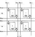
Fig. 1 is the block diagram of LCD (LCD) according to an exemplary embodiment of the present invention, Fig. 2 A shows the signal timing diagram of the signal of the output of gate drivers according to an exemplary embodiment of the present invention from Fig. 1, and Fig. 2 B to Fig. 2 E shows the schematic circuit of the operation of the LCD according to an exemplary embodiment of the present invention among Fig. 1.
With reference to Fig. 1, LCD 10 comprises liquid crystal panel 300, gate drivers 400, data driver 500, signal controller 600 and grayscale voltage generator 800.
Many display signal line G
11-G
N2And D
11-D
M2Comprise many gate lines G transmitting signal
11-G
N2Many data line D with transmission of data signals
11-D
M2Each pixel PX among a plurality of pixel PX is connected to many gate lines G
11-G
N2In a pair of corresponding gate line.For example, as shown in Figure 1, each pixel PX of first pixel column is connected to a pair of corresponding gate lines G
11And G
12In addition, each the pixel PX among a plurality of pixel PX is connected to many data line D
11-D
M2In a pair of corresponding data line.For example, as shown in Figure 1, each pixel PX of first pixel column is connected to a pair of corresponding data line D
11And D
12Therefore, each pixel PX is connected to a pair of corresponding gate lines G
11-G
N2With a pair of corresponding data line D
11-D
M2
As shown in Figure 1, many gate lines G
11-G
N2Extend along the first direction that is in line direction substantially, and many gate lines G
11-G
N2In the wall scroll gate line be parallel to each other and many data line D substantially
11-D
M2Along being in column direction substantially and extending perpendicular to the second direction of first direction, and many data line D
11-D
M2In the wall scroll data line be parallel to each other substantially.With reference to Fig. 5 to Fig. 8 liquid crystal panel 300 is described in more detail subsequently.
Still with reference to Fig. 1, signal controller 600 receives the redness (R) from the external graphics controller (not shown), green (G) and blue (B) viewdata signal, and reception is used to control a plurality of control signal V of the demonstration of R, G and B viewdata signal
Sync, H
Sync, MCLK and DE.Signal controller 600 is based on a plurality of control signal V
Sync, H
Sync, MCLK and DE produce grid control signal CONT1 and data controlling signal CONT2, and produce picture signal DAT based on R, G and B viewdata signal.Signal controller 600 provides picture signal DAT and the data controlling signal CONT2 that is produced to data driver 500, provides grid control signal CONT1 to gate drivers 400.
A plurality of control signal V
Sync, H
Sync, MCLK and DE comprise vertical synchronizing signal V
Sync, horizontal-drive signal H
Sync, master clock signal MCLK and data enable signal DE.
Grid control signal CONT1 is the signal of the operation of control gate driver 400, and for example, grid control signal CONT1 includes but not limited to: vertical synchronization start signal (not shown) is used to make the operation of gate drivers 400 to begin; Gate clock signal (not shown) is used to control gate-on voltage V
OnOutput timing; Output enable signal (not shown) is used to control gate-on voltage V
OnPulse width.
Now, describe in more detail from the sequential of the signal of gate drivers 400 outputs with reference to Fig. 2 A.
Shown in Fig. 2 A, in first frame, during very first time section T1 with gate-on voltage V
OnBe applied to first grid polar curve G
11, then, during the second time period T2 after very first time section T1 with gate-on voltage V
OnBe applied to the 4th gate lines G
22During the very first time section T1 and the second time period T2, with grid cut-off voltage V
OffBe applied to second grid line G
12With the 3rd gate lines G
21
In second frame, during the 3rd time period T3 with gate-on voltage V
OnBe applied to second grid line G
12, then, during the 4th time period T4 with gate-on voltage V
OnBe applied to the 3rd gate lines G
21During the 3rd time period T3 and the 4th time period T4, respectively with grid cut-off voltage V
OffBe applied to first grid polar curve G
11With the 4th gate lines G
22
When as mentioned above from gate drivers 400 output signals, pixel PX operates by following more detailed description.The operation of the signal that is applied to pixel PX more particularly, is described in more detail now with reference to Fig. 2 A to Fig. 2 E.For illustrative purposes, with four neighbor PX1, PX2, PX3 and PX4 among the pixel PX of discussion liquid crystal panel 300.In addition, Fig. 2 B to Fig. 2 E shows first data line to the, four data line D respectively
11, D
12, D
21And D
22Current potential, and show the polarity of first pixel to the, four pixel PX1, PX2, PX3 and PX4 respectively.
Hereinafter, will represent gate-on voltage V by label additional identification " (on) " to corresponding gate line
OnBe applied to the situation of corresponding gate line, for example, in relevant accompanying drawing, " G
11 (on)" expression gate-on voltage V
OnBe applied to gate lines G
11On the contrary, will represent grid cut-off voltage V by label additional identification " (off) " to corresponding gate line
OffBe applied to the situation of corresponding gate line, for example, in relevant accompanying drawing, G
11 (off)Expression grid cut-off voltage V
OffBe applied to gate lines G
11In addition, being applied to the positive polarity data voltage of data line and negative polarity data voltage will represent by positive sign (+) and negative sign (-) in corresponding data line label respectively, for example, in the accompanying drawing of being correlated with, D
11 (+)Expression positive polarity data voltage is applied to data line D
11At last, the situation that data line is floated will represent with letter " F ", for example, in relevant accompanying drawing, " D
11(F) " expression data line D
11Floated.
With reference to Fig. 2 B, during the very first time of first frame section T1 to first grid polar curve G
11Apply gate-on voltage V
On, during the very first time of first frame section T1 to second grid line G
12, the 3rd gate lines G
21With the 4th gate lines G
22Apply grid cut-off voltage V
OffAs a result, the first on-off element S1 and the 3rd on-off element S3 conducting.Therefore, respectively from the first data line D
11With the 4th data line D
22Data voltage is applied to the first pixel PX1 and the second pixel PX2.In addition, according to the exemplary embodiment of the present invention shown in Fig. 2 B, during the very first time of first frame section T1, the positive polarity data voltage is applied to the first data line D
11, the negative polarity data voltage is applied to the 4th data line D
22
As a result, the positive polarity data voltage is applied to the first pixel PX1, and the negative polarity data voltage is applied to the second pixel PX2, shown in Fig. 2 B.Because during the very first time of first frame section T1, second switch element S2, the 4th on-off element S4, the 6th on-off element S6 and octavo pass element S8 end, so the second data line D
12With the 3rd data line D
21Floated respectively.
In the exemplary embodiment, the current potential of positive polarity data voltage is pressed Vcom (Fig. 1) with respect to the direct current common-battery current potential is for just, and the current potential of negative polarity data voltage presses the current potential of Vcom for bearing with respect to the direct current common-battery.
With reference to Fig. 2 C, during the second time period T2 of first frame to the 4th gate lines G
22Apply gate-on voltage V
On, during the second time period T2 to first grid polar curve G
11, second grid line G
12With the 3rd gate lines G
21Apply grid cut-off voltage V
OffTherefore, the 6th on-off element S6 and octavo are closed element S8 conducting.Therefore, during the second time period T2 of first frame, respectively by the second data line D
12With the 3rd data line D
21Data voltage is applied to the 3rd pixel PX3 and the 4th pixel PX4.In the exemplary embodiment, the negative polarity data voltage is applied to the second data line D
12, the positive polarity data voltage is applied to the 3rd data line D
21Therefore, during the second time period T2 of first frame, will bear (-) polarity data voltage and be applied to the 3rd pixel PX3, and just (+) polarity data voltage is applied to the 4th pixel PX4.In addition, because during the second time period T2 of first frame, the first on-off element S1, the 3rd on-off element S3, the 5th on-off element S5 and minion pass element S7 end, so the first data line D
11With the 4th data line D
22Floated respectively.
With reference to Fig. 2 D, during the 3rd time period T3 of second frame to second grid line G
12Apply gate-on voltage V
OnTherefore, second switch element S2 and the 4th on-off element S4 conducting.Therefore, respectively from the second data line D
12With the 3rd data line D
21Data voltage is applied to the first pixel PX1 and the second pixel PX2.In the exemplary embodiment, the negative polarity data voltage is applied to the second data line D
12, the positive polarity data voltage is applied to the 3rd data line D
21Therefore, during the 3rd time period T3 of second frame, the negative polarity data voltage is applied to the first pixel PX1, and the positive polarity data voltage is applied to the second pixel PX2.Because during the 3rd time period T3 of second frame, the first on-off element S1, the 3rd on-off element S3, the 5th on-off element S5 and minion pass element S7 end respectively, so the first data line D
11With the 4th data line D
22Floated respectively.
With reference to Fig. 2 E, during the 4th time period T4 of second frame to the 3rd gate lines G
21Apply gate-on voltage V
OnTherefore, the 5th on-off element S5 and minion are closed element S7 conducting.Therefore, respectively data voltage is applied to the 3rd pixel PX3 and the 4th pixel PX4.In the exemplary embodiment, the positive polarity data voltage is applied to the first data line D
11, the negative polarity data voltage is applied to the 4th data line D
22Therefore, during the 4th time period T4 of second frame, the positive polarity data voltage is applied to the 3rd pixel PX3, and the negative polarity data voltage is applied to the 4th pixel PX4.In addition, because during the 4th time period T4 of second frame, second switch element S2, the 4th on-off element S4, the 6th on-off element S6 and octavo pass element S8 end respectively, so the second data line D
12With the 3rd data line D
21Floated.
As mentioned above, in the successive frame of LCD according to an exemplary embodiment of the present invention, carry out the some inversion driving method that alternately applies opposite polarity voltage to neighbor PX.In addition, alternately apply with respect to the direct current common-battery to pixel PX and press Vcom to have the data voltage of positive polarity and the data voltage of pressing Vcom to have negative polarity with respect to the direct current common-battery.Owing to be applied with the first data line D of positive polarity data voltage respectively
11With the 3rd data line D
21With the second data line D that is applied with the negative polarity data voltage respectively
12With the 4th data line D
22Be separated from each other and different,, thereby reduced the power consumption of LCD device effectively so the change in voltage between in corresponding correction data line or negative data line every is little.
In addition, when the positive polarity data voltage being applied to the first data line D respectively
11With the 3rd data line D
21, and the positive polarity data voltage is not applied to the second data line D respectively
12With the 4th data line D
22The time, reduced effectively data voltage is applied to the second data line D respectively
12With the 4th data line D
22The power consumption of Shi Suoxu.Equally, when the negative polarity data voltage being applied to the second data line D respectively
12With the 4th data line D
22, and the negative polarity data voltage is not applied to the first data line D respectively
11With the 3rd data line D
21The time, reduced effectively data voltage is applied to the first data line D
11With the 3rd data line D
21The power consumption of Shi Suoxu.
In the of the present invention selectable exemplary embodiment that will describe in more detail subsequently, can provide from the signal of gate drivers 400 supplies in the mode different with the above-mentioned mode of describing with reference to Fig. 2 A to Fig. 2 E.In addition, with the front optionally apply data voltage and exemplary embodiment that other data line is floated is different to some data lines, can apply positive polarity and/or negative polarity data voltage to all data lines simultaneously.In addition, in selectable exemplary embodiment of the present invention, can be to the first data line D
11With the 3rd data line D
21Apply the negative polarity data voltage, and can be to the second data line D
12With the 4th data line D
22Apply the positive polarity data voltage.Selectively, can be respectively to corresponding every couple first data line D
11With the 4th data line D
22And corresponding every couple second data line D
12With the 3rd data line D
21Apply the data voltage of same polarity.
At last, in exemplary embodiment of the present invention, for example, gate drivers 400 and/or data driver 500 can be directly installed on the liquid crystal panel 300 and have a plurality of integrated circuit (IC) chip (not shown), (TCP) form that perhaps can encapsulate with carrier band is installed on flexible print circuit (FPC) the film (not shown) that invests on the liquid crystal panel 300, but selectable exemplary embodiment is not limited thereto.For example, in selectable exemplary embodiment, gate drivers 400 and/or data driver 500 can be by system on glass (SOG) method and display signal line G
11-G
N2And D
11-D
M2Be integrated in together in the liquid crystal panel 300, but be not limited thereto.
The LCD of another exemplary embodiment according to the present invention is described in more detail with reference to Fig. 2 A, Fig. 3 A and Fig. 3 B hereinafter.Fig. 3 A and Fig. 3 B show the schematic circuit of the operation of the LCD of another exemplary embodiment according to the present invention.In Fig. 2 A to Fig. 2 E and Fig. 3 A and Fig. 3 B, identical label is represented same or analogous assembly; Therefore, will omit being repeated in this description hereinafter to these same or similar assemblies.Yet, shown in Fig. 3 A and Fig. 3 B and as more detailed description hereinafter, the on-off element S3 of the second pixel PX2 and the position of S4 are different from the on-off element S3 of the second pixel PX2 among Fig. 2 B to Fig. 2 E and the position of S4 respectively, and the on-off element S7 of the 4th pixel PX4 and the position of S8 are different from the on-off element S7 of the 4th pixel PX4 among Fig. 2 B to Fig. 2 E and the position of S8 respectively.
In the following description, suppose in Fig. 3 A and Fig. 3 B, respectively to corresponding first grid polar curve G
11, second grid line G
12, the 3rd gate lines G
21With the 4th gate lines G
22Apply the identical signal shown in Fig. 2 A.
With reference to Fig. 3 A, in first frame, first grid polar curve G
11With the 4th gate lines G
22Respectively by conducting sequentially (Fig. 2 A), thereby during very first time section T1, apply the positive polarity data voltage by the first on-off element S1 and the 3rd on-off element S3 respectively to the first pixel PX1 and the second pixel PX2 respectively.As shown in Figure 3A, during the second time period T2, close element S8 by the 6th on-off element S6 and octavo respectively and apply the negative polarity data voltage respectively to the 3rd pixel PX3 and the 4th pixel PX4.
With reference to Fig. 3 B, in second frame, second grid line G
12With the 3rd gate lines G
21Respectively by conducting sequentially (Fig. 2 A), thereby during the 3rd time period T3, apply the negative polarity data voltage by second switch element S2 and the 4th on-off element S4 respectively to the first pixel PX1 and the second pixel PX2 respectively.During the 4th time period T4, close element S7 by the 5th on-off element S5 and minion respectively and apply the positive polarity data voltage respectively to the 3rd pixel PX3 and the 4th pixel PX4.
Therefore, in the exemplary embodiment shown in Fig. 2 A, Fig. 3 A and Fig. 3 B, drive LCD by the row inverting method.Therefore, owing to be applied with the first data line D of positive polarity data voltage respectively
11With the 3rd data line D
21With the second data line D that is applied with the negative polarity data voltage respectively
12With the 4th data line D
22Be separated from each other and different, thus the voltage blocked operation between in the corresponding data line every occur in the little change in voltage scope, thereby reduced the power consumption of LCD basically.In addition, when the data line to reply mutually applies data voltage, data line is not applied data voltage, thereby can further reduce power consumption to other.
The LCD of the another exemplary embodiment according to the present invention is described in more detail with reference to Fig. 4 A to Fig. 4 C now.Fig. 4 A shows from the signal timing diagram of the signal of the gate drivers output of the LCD of the another exemplary embodiment according to the present invention, and Fig. 4 B and Fig. 4 C show the schematic circuit of the operation of the LCD according to an exemplary embodiment of the present invention in Fig. 4 A.
With reference to Fig. 4 A, in first frame, during very first time section T1 with gate-on voltage V
OnBe applied to first grid polar curve G
11, then, during the second time period T2 after very first time section T1 with gate-on voltage V
OnBe applied to the 3rd gate lines G
21During the very first time section T1 and the second time period T2, with grid cut-off voltage V
OffBe applied to second grid line G
12With the 4th gate lines G
22
In second frame, during the 3rd time period T3 with gate-on voltage V
OnBe applied to second grid line G
12, then, during the 4th time period T4 with gate-on voltage V
OnBe applied to the 4th gate lines G
22Shown in Fig. 4 A, during the 3rd time period T3 and the 4th time period T4, with grid cut-off voltage V
OffBe applied to first grid polar curve G respectively
11With the 3rd gate lines G
21
With reference to Fig. 4 B, in first frame, during very first time section T1, the positive polarity data voltage is applied to the first pixel PX1 by the first on-off element S1, by the 3rd on-off element S3 the negative polarity data voltage is applied to the second pixel PX2.During the second time period T2 of first frame, by the 5th on-off element S5 the positive polarity data voltage is applied to the 3rd pixel PX3, close element S7 by minion the negative polarity data voltage is applied to the 4th pixel PX4.
With reference to Fig. 4 C, in second frame, during the 3rd time period T3, the negative polarity data voltage is applied to the first pixel PX1 by second switch element S2, by the 4th on-off element S4 the positive polarity data voltage is applied to the second pixel PX2.During the 4th time period T4 of second frame, by the 6th on-off element S6 the negative polarity data voltage is applied to the 3rd pixel PX3, close element S8 by octavo the positive polarity data voltage is applied to the 4th pixel PX4.
Therefore, in the exemplary embodiment of the present invention shown in Fig. 4 A to Fig. 4 C, drive LCD by column inverting method.Therefore, owing to be applied with the first data line D of positive polarity data voltage respectively
11With the 3rd data line D
21With the second data line D that is applied with the negative polarity data voltage respectively
12With the 4th data line D
22Be separated from each other and different, occur in the little change in voltage scope, thereby reduced the power consumption of LCD so the voltage blocked operation between in the corresponding data line every changes.In addition, when data line being applied data voltage, and not when other applies data voltage to data line, further reduced power consumption to corresponding.
Hereinafter, with reference to Fig. 5 A and Fig. 5 B the data driver of LCD is according to an exemplary embodiment of the present invention described in more detail, in this data driver, to corresponding data line is applied positive polarity and/or negative polarity data voltage in, other right data line of floating.In order to be easy to describe, above the exemplary embodiment of the present invention among Fig. 2 A to Fig. 2 E is being described in more detail by the some inversion driving method, to describe exemplary embodiment with respect to LCD, hereinafter, will omit being repeated in this description same or similar assembly by this method operation.Yet, should be appreciated that data driver is not limited to exemplary embodiment of the present invention among Fig. 2 A to Fig. 2 E in greater detail hereinafter.On the contrary, the data driver of describing below with reference to Fig. 5 A and Fig. 5 B can be applicable to all exemplary embodiments of the present invention described here.
Fig. 5 A is the partial schematic circuit diagram that comprises the LCD of transmission gate according to an exemplary embodiment of the present invention, and Fig. 5 B shows the signal timing diagram of the operation of the transmission gate according to an exemplary embodiment of the present invention in Fig. 5 A.In the following description, for example, suppose that it is 0V that common-battery is pressed Vcom, but selectable exemplary embodiment is not limited thereto.
With reference to Fig. 5 A, data driver 500 receives picture signal DAT from signal controller 600 (Fig. 1), and the data voltage corresponding with picture signal DAT is supplied to the first raw data line D1 and the second raw data line D2.
Shown in Fig. 5 B, the data voltage that is applied to the first raw data line D1 during very first time section T1 is for (for example, positive polarity data voltage 0V) (for example, 3V), but is not limited thereto with respect to common-battery pressure Vcom; And the data voltage that during the second time period T2, is applied to the first raw data line D1 for press with respect to common-battery Vcom (for example, negative polarity data voltage 0V) (for example ,-3V), but be not limited thereto.
Refer again to Fig. 5 B, the data voltage that during very first time section T1, is applied to the second raw data line D2 for press with respect to common-battery Vcom (for example, negative polarity data voltage 0V) (for example ,-3V), but be not limited thereto; And the current potential that is applied to the second raw data line D2 during the second time period T2 is that (for example, positive polarity data voltage 0V) (for example, 3V), but is not limited thereto with respect to common-battery pressure Vcom.
Refer again to Fig. 5 A, according to the selection control signal/SEL that selects control signal SEL and/or counter-rotating, first transmission gate to the, four transmission gate TG1-TG4 offer data voltage first data line to the, four data line D respectively
11, D
12, D
21And D
22
More particularly, with reference to Fig. 5 B, when during very first time section T1, when the selection control signal/SEL that selects control signal SEL to reverse for height is low, the first transmission gate TG1 and the 4th transmission gate TG4 conducting, thereby during very first time section T1, will offer the first data line D from the voltage of the first raw data line D1
11, will offer the 4th data line D from the voltage of the second raw data line D2
22Therefore, during very first time section T1, to the first data line D
11Apply the voltage of 3V, to the 4th data line D
22Apply-voltage of 3V.In addition, the second data line D
12With the 3rd data line D
21Floated respectively, therefore, the second data line D
12With the 3rd data line D
21Current potential for example can be approximately 0V, but be not limited thereto.
When during the second time period T2, when selection control signal SEL is high for the low selection control signal/SEL that reverses, the second transmission gate TG2 and the 3rd transmission gate TG3 conducting, thus during the second time period T2, will offer the second data line D from the voltage of the first raw data line D1
12, will offer the 3rd data line D from the voltage of the second raw data line D2
21Therefore, during the second time period T2, to the second data line D
12Apply-voltage of 3V, to the 3rd data line D
21Apply the voltage of 3V.In addition, the first data line D
11With the 4th data line D
22Floated respectively, therefore, the first data line D
11With the 4th data line D
22Current potential for example can be approximately 0V, but be not limited thereto.
Refer again to Fig. 5 A, for example, as mentioned above, can data driver 500 be integrated in the liquid crystal panel 300 (Fig. 1), but be not limited thereto by the SOG method.In this case, data driver 500 can correspondingly integrate with first transmission gate to the, four transmission gate TG1-TG4.
In selectable exemplary embodiment, the selection control signal/SEL of the connection status of first transmission gate to the, four transmission gate TG1-TG4, selection control signal SEL and counter-rotating can change.Therefore, when the connection status of first transmission gate to the, four transmission gate TG1-TG4, select the selection control signal/SEL of control signal SEL and counter-rotating be different from the connection status of first transmission gate to the, the four transmission gate TG1-TG4 shown in Fig. 5 A, when selecting the selection control signal of control signal SEL and counter-rotating/SEL, with spirit of the present invention and/or the corresponding to situation of scope under, can be different from the waveform shown in Fig. 5 B from the waveform of the signal of data driver 500 output from the signal of data driver 500 outputs.
Therefore, as described later, the invention is not restricted to illustrative exemplary embodiment described herein.For example, in selectable exemplary embodiment, first transmission gate to the, four transmission gate TG1-TG4 can be set.On the contrary, data driver 500 can be directly respectively to first data line to the, four data line D
11-D
22Data voltage is provided.In other words, in selectable exemplary embodiment of the present invention, data driver 500 can be carried out the function of first transmission gate to the, four transmission gate TG1-TG4 respectively.
Hereinafter, with reference to Fig. 6 to Fig. 8 the LCD that shows substrate according to an exemplary embodiment of the present invention and comprise this demonstration substrate is described in more detail.Fig. 6 is the plane figure that shows substrate according to an exemplary embodiment of the present invention and comprise the LCD of this demonstration substrate, Fig. 7 is showing substrate according to an exemplary embodiment of the present invention and comprising the partial sectional view of VII-VII ' the line intercepting among the LCD of this demonstration substrate in Fig. 6, and Fig. 8 is showing substrate according to an exemplary embodiment of the present invention and comprising the partial sectional view that the VIII-VIII ' line among the LCD of this demonstration substrate intercepts in Fig. 6.For purposes of illustration, as shown in Figure 6, will with regard to two neighbors among the LCD exemplary embodiment be described hereinafter.In addition, exemplary embodiment will be described to Transflective LCD hereinafter, but selectable exemplary embodiment of the present invention is not limited thereto.In addition, in the following description, illustrated and described the structure of the pixel that comprises two on-off elements, these two on-off elements connect two corresponding gate lines and two corresponding data lines, but selectable exemplary embodiment of the present invention is not limited thereto.
Now, describe first display panel 100 in more detail, for example show substrate according to an exemplary embodiment of the present invention with reference to Fig. 6 to Fig. 8.
For example, by monox (SiO
2) or silicon nitride (SiN
x) barrier film 111 (but being not limited thereto) made is formed on the transparent dielectric base 110.For example, barrier film 111 can have double-decker, but is not limited thereto.
For example, a plurality of semiconductor island 151a and the 151b (but being not limited thereto) that is made by polysilicon is formed on the barrier film 111. Semiconductor island 151a and 151b among a plurality of semiconductor island 151a and the 151b comprise extrinsic region and intrinsic region, and wherein, extrinsic region contains conductive impurity, and the intrinsic region contains conductive impurity hardly with respect to the extrinsic region of semiconductor island 151a and 151b.In addition, impurity range comprises heavily doped region and light doping section.
The intrinsic region of corresponding semiconductor island 151a and 151b comprises channel region 154a and 154b.As shown in Figure 7, the heavy doping impurity range comprises source region 153a, mesozone 156a and the drain region 155a that separates with respect to channel region 154a, reaches source region 153b, the mesozone 156b and the drain region 155b that separate with respect to channel region 154b.As shown in Figure 7, lightly-doped impurity area 152a is arranged between channel region 154a and the source region 153a, between channel region 154a and the drain region 155a and between channel region 154a and the mesozone 156a, lightly-doped impurity area 152b is arranged between channel region 154b and the source region 153b, between channel region 154b and the drain region 155b and between channel region 154b and the mesozone 156b, compare with the horizontal length of 155b and mesozone 156a and 156b with 153b, drain region 155a with 154b, source region 153a with channel region 154a, the horizontal length of each among lightly-doped impurity area 152a and the 152b is relative little.Lightly-doped impurity area 152a is arranged between among source region 153a, channel region 154a, mesozone 156a and the drain region 155a each, and lightly-doped impurity area 152b is arranged between among source region 153b, channel region 154b, mesozone 156b and the drain region 155b each.Channel region 154a and 154b are known as lightly doped drain (LDD) district.For the sake of brevity, will omit the formation in LDD district at this.
Conductive impurity comprises such as the p type impurity of boron (B) or gallium (Ga) with such as the N type impurity of phosphorus (P) or arsenic (As), but is not limited thereto.Lightly-doped impurity area 152a and 152b prevent to occur at the thin film transistor (TFT) place leakage current or penetration phenomenon (punch through), and in selectable exemplary embodiment, for example available do not have the deviate region of impurity to replace lightly-doped impurity area 152a and 152b.
For example by SiN
xOr SiO
2The gate insulator of making 140 is formed on a plurality of semiconductor island 151a and 151b and the barrier film 111.
Having the gate line 121a of gate electrode 124a, the gate line 121b with 124b of gate electrode, storage electrode line 131 and light blocking pattern 127 is formed on the gate insulator 140.
Gate line 121a and 121b transmission signal, and extend along first horizontal direction substantially.Gate electrode 124a and 124b extend upward from gate line 121a and 121b, and with semiconductor island 151a with 151b intersects and stacked with corresponding channel region 154a and 154b.Every among gate line 121a and the 121b can have the pad (not shown), and described pad has and is used for the large tracts of land that is connected with another layer or external drive circuit (not shown).
Storage electrode line 131 receives predetermined voltage (for example, the common-battery that is applied to common electrode 270 is pressed, and this will be described in more detail subsequently), and comprises extension 137, compares with the area of storage electrode line 131, and the area of this extension 137 is big relatively.
For example, gate line 121a, gate line 121b, storage electrode line 131 and light blocking pattern 127 can be such as aluminium (Al) or Al alloy contain the Al metal, such as silver (Ag) or Ag alloy contain the Ag metal, such as copper (Cu) or Cu alloy contain the Cu metal, such as molybdenum (Mo) or Mo alloy contain Mo metal, chromium (Cr), tantalum (Ta), titanium (Ti) or tungsten (W), but be not limited thereto.Selectively, gate line 121a, gate line 121b and storage electrode line 131 can have the sandwich construction of the two-layer different conducting film (not shown) that comprises different physical characteristicss.In this two-layer different conducting film, one deck conducting film for example can be by making such as the low resistivity metal that contains the Al metal, contains the Ag metal or contain the Mo metal, another layer conducting film for example can be made such as containing Mo metal, Cr, Ta or Ti by the material that has a good contact performance with other material, but be not limited thereto, wherein, described other material for example is tin indium oxide (ITO), indium zinc oxide (IZO) or other similar material.In the exemplary embodiment, for example, sandwich construction comprises two-layer different conducting film (for example, following Cr film and last Al or Al alloy film perhaps descend Al or Al alloy film and last Mo or Mo alloy film), but is not limited thereto.In addition, in selectable exemplary embodiment of the present invention, gate line 121a and 121b can be made by other various metals and/or conductor.
For example, interlayer dielectric 160 is made by inorganic insulator, organic insulator or low dielectric insulation material such as silicon nitride or monox, but is not limited thereto.In the exemplary embodiment, the specific inductive capacity of organic insulator or low dielectric insulation material is about 4.0 or lower, but is not limited thereto.The example of low dielectric insulation material for example comprises by what plasma enhanced chemical vapor deposition (PECVD) formed and (has added the α-Si:C:O of carbon (C) and oxygen (O) and added O and α-the Si:F:O of fluorine (F) among the α-Si), still be not limited thereto at amorphous silicon.In selectable exemplary embodiment of the present invention, for example, interlayer dielectric 160 can be made and can be flattened by the organic insulator with photosensitivity, but is not limited thereto.
A plurality of contact hole 165b that expose contact hole 163a, the contact hole 163b that exposes source region 153b, the contact hole 165a that exposes drain region 155a and the exposure drain region 155b of source region 153a respectively pass interlayer dielectric 160 and gate insulator 140 forms.
Ying Dui data line 171a and 171b intersect with the gate line 121a and the 121b of reply mutually mutually, and comprise respectively by contact hole 163a and be connected to the source electrode 173a of source region 153a and be connected to the source electrode 173b of source region 153b by contact hole 163b.
In the exemplary embodiment, as shown in Figure 8, at least a portion of data line 171a and 171b and light blocking pattern 127 is stacked.As mentioned above, light blocking pattern 127 prevents that light from leaking.Therefore, the aperture opening ratio that has increased LCD with stacked data line 171a of light blocking pattern 127 and 171b.In one exemplary embodiment, as shown in Figure 8, light blocking pattern 127 is enough wide with stacked fully with data line 171b and 172a, but is not limited thereto in selectable exemplary embodiment of the present invention.
In the exemplary embodiment, for example, data line 171a, 171b, 172a and the 172b of transmission of data signals, drain electrode 175a and 175b and extension 177 are made by refractory metal or its alloy such as Mo, Cr, Ta or Ti, but are not limited thereto.Selectively, data line 171a, 171b, 172a and the 172b of transmission of data signals, drain electrode 175a and 175b and extension 177 can have sandwich construction, and this sandwich construction comprises following film of being made by refractory metal and the last film of being made by low resistivity metal.In selectable exemplary embodiment of the present invention, for example, the example of sandwich construction comprises the double-decker with following Cr or Mo or Mo alloy film and last Al or Al alloy film, and has the three-decker of following Mo or Mo alloy film, middle Al or Al alloy film and last Mo film, but is not limited thereto.
As shown in Figure 7, the contact hole 185 that exposes the extension 137 of storage electrode line 131 passes passivation layer 180 formation.
A plurality of pixel electrodes 192 and 196 are formed on the passivation layer 180.Reflectance coating 194 is formed on in pixel electrode 192 and 196 each.Pixel electrode 192 is by making such as the transparent conductive material of ITO and indium zinc oxide IZO, and reflectance coating 194 is by making such as the reflective metals that contains Al metal (for example, Al or Al alloy) or contain Ag metal (for example, Ag or Ag alloy).As shown in Figure 7, reflectance coating 194 is stacked with at least a portion of gate line 121b.In the exemplary embodiment, for example, reflectance coating 194 can be positioned at liquid crystal layer 3 below, and reflectance coating 194 can be positioned at pixel electrode 192 below.
Because the irregularity that forms on film 180q on the passivation layer 180 makes pixel electrode 192 and reflectance coating 194 have uneven surface.Reflectance coating 194 has the transmission window 195 (Fig. 8) that exposes pixel electrode 192.
LCD comprises transmission area TA and the echo area RA that is limited by pixel electrode 192 and reflectance coating 194 according to an exemplary embodiment of the present invention.More particularly, the transmission window 195 (Fig. 8) that does not for example form reflectance coating 194 is transmission area TA, and the zone with pixel electrode 192 and reflectance coating 194 is echo area RA (Fig. 7 and Fig. 8).
In addition, transmission area TA be LCD in tft array panel 100, second display panel 200 and LCD layer 3 the expose portion that is arranged on pixel electrode 192 a plurality of parts up and down (for example, pixel electrode 192 not in the part under reflectance coating 194 on the reflectance coating 194 or not), and echo area RA be LCD be arranged on a plurality of parts of reflectance coating about in the of 194.In transmission area TA, pass first display panel 100 and liquid crystal layer 3 in proper order from the incident light of the back surface launching of LCD, then from 200 outgoing of second display panel, thus display image.In the RA of echo area, pass second display panel 200 and liquid crystal layer 3 in proper order by the exterior light of supplying previously of LCD, reflected by the front of the reflectance coating 194 of first display panel 100 then towards LCD.After reflection, light returns once more wears liquid crystal layer 3, then from 200 outgoing of second display panel, thus display image.
As shown in Figure 8, black matrix 220 can be stacked with at least a portion of every among data line 171b and the 172a.Stacked area is big more, and it is good more that aperture opening ratio becomes.
Described exemplary embodiment of the present invention, wherein, LCD comprises light blocking pattern 127 that is arranged on first display panel 100 and the black matrix 220 that is arranged on second display panel 200.Yet selectable exemplary embodiment of the present invention is not limited thereto, and LCD can comprise any one in light blocking pattern 127 and the black matrix 220.
As shown in Figure 7 and Figure 8, a plurality of color filters 230 are formed on substrate 210 and the black matrix 220, and are arranged to pixel region stacked.
Showing substrate according to an exemplary embodiment of the present invention and comprising among the LCD of this demonstration substrate that the data line that is applied with the data line of positive polarity data voltage and is applied with the negative polarity data voltage is separated from each other and is different.Therefore, the change in voltage between every in the corresponding data line is little, thereby has reduced the power consumption of LCD effectively.
In addition, in the LCD that has dot structure (having two gate lines and two data lines) according to an exemplary embodiment of the present invention, owing at least a portion of every gate line and reflectance coating is stacked, at least a portion of every data line and light blocking pattern and/or black matrix is stacked, so increased the aperture opening ratio of LCD.
Therefore, according to exemplary embodiment of the present invention as described herein, increased show substrate and comprise the aperture opening ratio of LCD of this demonstration substrate in, reduced the demonstration substrate and comprised the power consumption of the LCD of this demonstration substrate.
The present invention should not be understood that to be confined to exemplary embodiment set forth herein.On the contrary, provide these exemplary embodiments to make that the disclosure will be thoroughly and completely, and will convey to those skilled in the art to design of the present invention fully.Therefore, expectation be, that go out as shown and nonrestrictively consider the exemplary embodiment described aspect all here.
In addition, though specifically illustrate and described the present invention with reference to exemplary embodiment of the present invention, but will be understood by those skilled in the art that, under the situation that does not break away from the spirit and scope of the present invention that are defined by the claims, can make in form and the various variations on the details at this.
Claims (21)
1, a kind of LCD comprises:
The first correction data line and the second correction data line, every supply positive polarity data voltage in the first correction data line and the second correction data line;
The first negative data line and the second negative data line, every supply negative polarity data voltage in the first negative data line and the second negative data line;
First pixel, be connected to first grid polar curve and second grid line, wherein, when making the work of first pixel by first grid forward voltage from first grid polar curve, first pixel is supplied the positive polarity data voltage from the first correction data line, when making the work of first pixel by the second grid forward voltage from the second grid line, first pixel is supplied the negative polarity data voltage from the first negative data line;
Second pixel, be connected to first grid polar curve and second grid line, wherein, when making the work of second pixel by first grid forward voltage from first grid polar curve, second pixel is supplied the negative polarity data voltage from the second negative data line, when making the work of second pixel by the second grid forward voltage from the second grid line, second pixel is supplied the positive polarity data voltage from the second correction data line.
2, LCD as claimed in claim 1, wherein, the current potential that the current potential of positive polarity data voltage is pressed with respect to the direct current common-battery is being for just, and the current potential that the current potential of negative polarity data voltage is pressed with respect to the direct current common-battery is for bearing.
3, LCD as claimed in claim 1, wherein, first pixel and second pixel include:
First on-off element is worked by the first grid forward voltage;
The second switch element is worked by the second grid forward voltage;
Pixel electrode is connected to first on-off element and second switch element, wherein, applies positive polarity data voltage or negative polarity data voltage by first on-off element or second switch element to pixel electrode.
4, LCD as claimed in claim 2, wherein, first pixel and second pixel include:
First on-off element is worked by the first grid forward voltage;
The second switch element is worked by the second grid forward voltage;
Pixel electrode is connected to first on-off element and second switch element, wherein, applies positive polarity data voltage or negative polarity data voltage by first on-off element or second switch element to pixel electrode;
Common electrode, and pixel-oriented electrode relative with pixel electrode, and be applied in direct current common-battery pressure;
Liquid crystal layer places between pixel electrode and the common electrode;
Reflectance coating is arranged between pixel electrode and the liquid crystal layer.
5, LCD as claimed in claim 4, wherein, at least a portion of at least one in reflectance coating and first grid polar curve and the second grid line is stacked.
6, LCD as claimed in claim 4 also comprises:
Substrate, wherein, first grid polar curve and second grid line are formed in the described substrate;
The light blocking pattern is formed in the substrate between the adjacent pixel electrodes, and wherein, at least a portion of light blocking pattern and the first correction data line or the first negative data line are stacked, and stacked with the second correction data line or the second negative data line.
7, LCD as claimed in claim 4 also comprises the black matrix that is arranged on the common electrode, and wherein, at least a portion of black matrix and the first correction data line or the first negative data line are stacked, and stacked with the second correction data line or the second negative data line.
8, LCD as claimed in claim 1, wherein, when from the first correction data line supply positive polarity data voltage, the first negative data line is floated; When from the first negative data line supply negative polarity data voltage, the first correction data line is floated.
9, LCD as claimed in claim 1 also comprises:
Data driver provides the positive polarity data voltage according to picture signal to the first correction data line and the second correction data line, perhaps provides the negative polarity data voltage to the first negative data line and the second negative data line;
A plurality of transmission gates, when providing the positive polarity data voltage from data driver, a plurality of transmission gates provide the positive polarity data voltage to the first correction data line and the second correction data line, when providing the negative polarity data voltage from data driver, a plurality of transmission gates provide the negative polarity data voltage to the first negative data line and the second negative data line.
10, LCD as claimed in claim 9, wherein, when providing the positive polarity data voltage from data driver, transmission gate does not provide the positive polarity data voltage to the first negative data line and the second negative data line, when providing the negative polarity data voltage from data driver, transmission gate does not provide the negative polarity data voltage to the first correction data line and the second correction data line.
11, LCD as claimed in claim 1 also comprises:
The 3rd gate line and the 4th gate line;
The 3rd pixel, be connected to the 3rd gate line, the 4th gate line, the first correction data line and the first negative data line, wherein, when making the work of the 3rd pixel by the 3rd gate-on voltage from the 3rd gate line, the 3rd pixel is supplied the positive polarity data voltage from the first correction data line, when making the work of the 3rd pixel by the 4th gate-on voltage from the 4th gate line, the 3rd pixel is supplied the negative polarity data voltage from the first negative data line;
The 4th pixel, be connected to the 3rd gate line, the 4th gate line, the second correction data line and the second negative data line, wherein, when making the work of the 4th pixel by the 3rd gate-on voltage from the 3rd gate line, the 4th pixel is supplied the negative polarity data voltage from the second negative data line, when making the work of the 4th pixel by the 4th gate-on voltage from the 4th gate line, the 4th pixel is supplied the positive polarity data voltage from the second correction data line.
12, LCD as claimed in claim 1 also comprises:
The 3rd gate line and the 4th gate line;
The 3rd pixel, be connected to the 3rd gate line, the 4th gate line, the first correction data line and the first negative data line, wherein, when making the work of the 3rd pixel by the 3rd gate-on voltage from the 3rd gate line, the 3rd pixel is supplied the negative polarity data voltage from the first negative data line, when making the work of the 3rd pixel by the 4th gate-on voltage from the 4th gate line, the 3rd pixel is supplied the positive polarity data voltage from the first correction data line;
The 4th pixel, be connected to the 3rd gate line, the 4th gate line, the second correction data line and the second negative data line, wherein, when making the work of the 4th pixel by the 3rd gate-on voltage from the 3rd gate line, the 4th pixel is supplied the positive polarity data voltage from the second correction data line, when making the work of the 4th pixel by the 4th gate-on voltage from the 4th gate line, the 4th pixel is supplied the negative polarity data voltage from the second negative data line.
13, LCD as claimed in claim 1 wherein, in the different frame in a plurality of frames of LCD, all provides first grid forward voltage and second grid forward voltage.
14, a kind of demonstration substrate comprises:
Dielectric base;
First grid polar curve and second grid line are formed on the dielectric base;
First data line and second data line are formed on the dielectric base, and all intersect with first grid polar curve and second grid line;
The first film transistor is connected to the first grid polar curve and first data line, and has first drain electrode;
Second thin film transistor (TFT) is connected to the second grid line and second data line, and has second drain electrode;
First pixel electrode is connected to first drain electrode and second drain electrode;
Reflectance coating, wherein, at least a portion of at least a portion of reflectance coating and first pixel electrode is stacked.
15, demonstration substrate as claimed in claim 14, wherein, at least a portion of one of reflectance coating and first grid polar curve and second grid line is stacked.
16, demonstration substrate as claimed in claim 14, wherein, first pixel electrode is arranged between first data line and second data line.
17, demonstration substrate as claimed in claim 14 also comprises the light blocking pattern that is formed on the dielectric base, and wherein, at least a portion of one of at least a portion of light blocking pattern and first data line and second data line is stacked.
18, demonstration substrate as claimed in claim 14, wherein, when when first data line applies data voltage, second data line is floated.
19, demonstration substrate as claimed in claim 14 also comprises:
The 3rd data line and the 4th data line;
The 3rd thin film transistor (TFT) is connected to first grid polar curve and the 3rd data line, and has the 3rd drain electrode;
The 4th thin film transistor (TFT) is connected to second grid line and the 4th data line, and has the 4th drain electrode;
Second pixel electrode is connected to the 3rd drain electrode and the 4th drain electrode.
20, demonstration substrate as claimed in claim 19, wherein, first pixel electrode is arranged between first data line and second data line, and second pixel electrode is arranged between the 3rd data line and the 4th data line.
21, demonstration substrate as claimed in claim 19, also comprise the light blocking pattern, described light blocking pattern is formed on the dielectric base that is arranged between first pixel electrode and second pixel electrode, wherein, at least a portion of one of one of at least a portion of light blocking pattern and first data line and second data line and the 3rd data line and the 4th data line is stacked.
Applications Claiming Priority (2)
| Application Number | Priority Date | Filing Date | Title |
|---|---|---|---|
| KR10-2007-0032893 | 2007-04-03 | ||
| KR1020070032893A KR20080089992A (en) | 2007-04-03 | 2007-04-03 | Display substrate and liquid crystal display comprising the same |
Publications (1)
| Publication Number | Publication Date |
|---|---|
| CN101281334A true CN101281334A (en) | 2008-10-08 |
Family
ID=39826493
Family Applications (1)
| Application Number | Title | Priority Date | Filing Date |
|---|---|---|---|
| CNA2008100805838A Pending CN101281334A (en) | 2007-04-03 | 2008-02-22 | Display substrate and LCD with the same |
Country Status (4)
| Country | Link |
|---|---|
| US (1) | US20080246720A1 (en) |
| JP (1) | JP2008257164A (en) |
| KR (1) | KR20080089992A (en) |
| CN (1) | CN101281334A (en) |
Cited By (7)
| Publication number | Priority date | Publication date | Assignee | Title |
|---|---|---|---|---|
| CN101963723B (en) * | 2009-07-22 | 2012-05-30 | 北京京东方光电科技有限公司 | TFT-LCD (Thin Film Transistor Liquid Crystal Display) array substrate and manufacturing method thereof |
| CN102789756A (en) * | 2011-05-18 | 2012-11-21 | 三星电子株式会社 | Method of driving display panel and display apparatus for performing the method |
| CN105761703A (en) * | 2016-05-20 | 2016-07-13 | 京东方科技集团股份有限公司 | Array substrate, display device and charging control method |
| WO2017118103A1 (en) * | 2016-01-05 | 2017-07-13 | 京东方科技集团股份有限公司 | Thin-film transistor, driving method therefor, array substrate, and display device |
| CN107331363A (en) * | 2017-08-23 | 2017-11-07 | 京东方科技集团股份有限公司 | A kind of array base palte, its driving method and display device |
| CN109817138A (en) * | 2017-11-19 | 2019-05-28 | 联咏科技股份有限公司 | The method of sub-pixel on display screen, display drive apparatus and driving display screen |
| CN113409718A (en) * | 2021-05-27 | 2021-09-17 | 惠科股份有限公司 | Display panel and display device |
Families Citing this family (10)
| Publication number | Priority date | Publication date | Assignee | Title |
|---|---|---|---|---|
| US8830411B2 (en) * | 2009-01-16 | 2014-09-09 | Samsung Display Co., Ltd. | Array substrate and method of manufacturing the same |
| US8169559B2 (en) * | 2009-01-16 | 2012-05-01 | Samsung Electronics Co., Ltd. | Array substrate and method of manufacturing the same |
| EP2538270A1 (en) * | 2009-04-15 | 2012-12-26 | Samsung Electronics Co., Ltd. | Array substrate and method of manufacturing the same |
| KR101641958B1 (en) | 2010-03-10 | 2016-07-25 | 삼성디스플레이 주식회사 | Liquid crsytal display |
| TWI423216B (en) * | 2010-11-15 | 2014-01-11 | Au Optronics Corp | Displayer and pixel circuit thereof |
| CN104391409A (en) * | 2010-11-24 | 2015-03-04 | 友达光电股份有限公司 | Display and pixel circuit thereof |
| JP2016184098A (en) * | 2015-03-26 | 2016-10-20 | 株式会社ジャパンディスプレイ | Display |
| CN105116651B (en) * | 2015-09-01 | 2019-07-02 | 深圳市华星光电技术有限公司 | BOA type liquid crystal display panel |
| CN107301847B (en) * | 2017-06-29 | 2018-08-28 | 惠科股份有限公司 | A kind of driving method of display panel, driving device and display device |
| CN109755258B (en) * | 2017-11-08 | 2021-02-19 | 元太科技工业股份有限公司 | Pixel array substrate and display device |
Family Cites Families (2)
| Publication number | Priority date | Publication date | Assignee | Title |
|---|---|---|---|---|
| KR100312760B1 (en) * | 1999-02-24 | 2001-11-03 | 윤종용 | Liquid Crystal Display panel and Liquid Crystal Display device and Driving method thereof |
| KR101230301B1 (en) * | 2005-07-19 | 2013-02-06 | 삼성디스플레이 주식회사 | Liquid crystal display and driving method thereof |
-
2007
- 2007-04-03 KR KR1020070032893A patent/KR20080089992A/en not_active Application Discontinuation
- 2007-08-31 JP JP2007225349A patent/JP2008257164A/en not_active Withdrawn
-
2008
- 2008-01-21 US US12/017,165 patent/US20080246720A1/en not_active Abandoned
- 2008-02-22 CN CNA2008100805838A patent/CN101281334A/en active Pending
Cited By (12)
| Publication number | Priority date | Publication date | Assignee | Title |
|---|---|---|---|---|
| CN101963723B (en) * | 2009-07-22 | 2012-05-30 | 北京京东方光电科技有限公司 | TFT-LCD (Thin Film Transistor Liquid Crystal Display) array substrate and manufacturing method thereof |
| CN102789756A (en) * | 2011-05-18 | 2012-11-21 | 三星电子株式会社 | Method of driving display panel and display apparatus for performing the method |
| CN102789756B (en) * | 2011-05-18 | 2016-09-07 | 三星显示有限公司 | Drive the method for display floater and perform the display device of the method |
| WO2017118103A1 (en) * | 2016-01-05 | 2017-07-13 | 京东方科技集团股份有限公司 | Thin-film transistor, driving method therefor, array substrate, and display device |
| US10236393B2 (en) | 2016-01-05 | 2019-03-19 | Boe Technology Group Co., Ltd. | TFT, method for driving the same, array substrate and display device |
| CN105761703A (en) * | 2016-05-20 | 2016-07-13 | 京东方科技集团股份有限公司 | Array substrate, display device and charging control method |
| CN105761703B (en) * | 2016-05-20 | 2018-05-25 | 京东方科技集团股份有限公司 | Array substrate, display device and charge control method |
| CN107331363A (en) * | 2017-08-23 | 2017-11-07 | 京东方科技集团股份有限公司 | A kind of array base palte, its driving method and display device |
| CN109817138A (en) * | 2017-11-19 | 2019-05-28 | 联咏科技股份有限公司 | The method of sub-pixel on display screen, display drive apparatus and driving display screen |
| CN113409718A (en) * | 2021-05-27 | 2021-09-17 | 惠科股份有限公司 | Display panel and display device |
| CN113409718B (en) * | 2021-05-27 | 2022-02-18 | 惠科股份有限公司 | Display panel and display device |
| WO2022247272A1 (en) * | 2021-05-27 | 2022-12-01 | 惠科股份有限公司 | Display panel and display apparatus |
Also Published As
| Publication number | Publication date |
|---|---|
| KR20080089992A (en) | 2008-10-08 |
| US20080246720A1 (en) | 2008-10-09 |
| JP2008257164A (en) | 2008-10-23 |
Similar Documents
| Publication | Publication Date | Title |
|---|---|---|
| CN101281334A (en) | Display substrate and LCD with the same | |
| KR101061854B1 (en) | LCD and its driving method | |
| CN100538783C (en) | Display device | |
| TWI432853B (en) | Liquid crystal display | |
| CN1959480B (en) | Liquid crystal display | |
| US8964140B2 (en) | Liquid crystal display | |
| US9158168B2 (en) | Display device and driving method thereof | |
| CN100357815C (en) | Liquid crystal display and its driving method | |
| TWI522709B (en) | Liquid crystal display apparatus with wide viewing angle | |
| CN100547474C (en) | Display device | |
| US8049699B2 (en) | Liquid crystal display apparatus having storage electrodes overlapping only some sub-pixels | |
| KR101471550B1 (en) | Panel, liquid crystal display including the same and method for manufacturing thereof | |
| US8638324B2 (en) | Display device and driving method thereof | |
| US8334831B1 (en) | Array substrate and liquid crystal display device having the same | |
| KR101240647B1 (en) | Liquid crystal display | |
| KR20110049556A (en) | Thin film transistor display panel and method of manufacturing the same | |
| TWI406068B (en) | Array substrate and display device having the same | |
| US7486367B2 (en) | Display panel including signal lines having multiple conductive lines | |
| US20080204399A1 (en) | Driving method for electrophoretic display | |
| US10495918B2 (en) | Display device comprising color filter | |
| US7843539B2 (en) | Thin film transistor substrate and liquid crystal display having the same | |
| US8169583B2 (en) | Thin film transistor array panel and liquid crystal display having the same | |
| US8711302B2 (en) | Liquid crystal display | |
| CN101008758A (en) | Switch element array panel and liquid crystal display | |
| US10209541B2 (en) | Liquid crystal display device and method for manufacturing the same |
Legal Events
| Date | Code | Title | Description |
|---|---|---|---|
| C06 | Publication | ||
| PB01 | Publication | ||
| C10 | Entry into substantive examination | ||
| SE01 | Entry into force of request for substantive examination | ||
| AD01 | Patent right deemed abandoned |
Effective date of abandoning: 20081008 |
|
| C20 | Patent right or utility model deemed to be abandoned or is abandoned |