CN101263617A - Light-emitting device, and method for the manufacture thereof - Google Patents
Light-emitting device, and method for the manufacture thereof Download PDFInfo
- Publication number
- CN101263617A CN101263617A CNA200680033869XA CN200680033869A CN101263617A CN 101263617 A CN101263617 A CN 101263617A CN A200680033869X A CNA200680033869X A CN A200680033869XA CN 200680033869 A CN200680033869 A CN 200680033869A CN 101263617 A CN101263617 A CN 101263617A
- Authority
- CN
- China
- Prior art keywords
- group
- resilient coating
- luminescent device
- acidic
- luminescent layer
- Prior art date
- Legal status (The legal status is an assumption and is not a legal conclusion. Google has not performed a legal analysis and makes no representation as to the accuracy of the status listed.)
- Pending
Links
- 238000000034 method Methods 0.000 title claims abstract description 25
- 238000004519 manufacturing process Methods 0.000 title abstract description 5
- 239000002253 acid Substances 0.000 claims abstract description 37
- 229920001940 conductive polymer Polymers 0.000 claims abstract description 10
- 239000002322 conducting polymer Substances 0.000 claims abstract description 9
- 239000011248 coating agent Substances 0.000 claims description 50
- 238000000576 coating method Methods 0.000 claims description 50
- 229920000642 polymer Polymers 0.000 claims description 27
- 230000032050 esterification Effects 0.000 claims description 21
- 238000005886 esterification reaction Methods 0.000 claims description 21
- 239000003795 chemical substances by application Substances 0.000 claims description 18
- GKASDNZWUGIAMG-UHFFFAOYSA-N triethyl orthoformate Chemical group CCOC(OCC)OCC GKASDNZWUGIAMG-UHFFFAOYSA-N 0.000 claims description 18
- 238000006243 chemical reaction Methods 0.000 claims description 16
- 125000000542 sulfonic acid group Chemical group 0.000 claims description 12
- 238000004528 spin coating Methods 0.000 claims description 8
- 238000007641 inkjet printing Methods 0.000 claims description 6
- 125000000217 alkyl group Chemical group 0.000 claims description 4
- 125000003118 aryl group Chemical group 0.000 claims description 4
- 229910052799 carbon Inorganic materials 0.000 claims description 4
- 125000004432 carbon atom Chemical group C* 0.000 claims description 4
- 125000006165 cyclic alkyl group Chemical group 0.000 claims description 4
- 125000004435 hydrogen atom Chemical group [H]* 0.000 claims description 4
- 101001102158 Homo sapiens Phosphatidylserine synthase 1 Proteins 0.000 claims 2
- 102100039298 Phosphatidylserine synthase 1 Human genes 0.000 claims 2
- 229920001609 Poly(3,4-ethylenedioxythiophene) Polymers 0.000 claims 2
- 239000000872 buffer Substances 0.000 abstract description 5
- 230000002378 acidificating effect Effects 0.000 abstract description 4
- 238000005424 photoluminescence Methods 0.000 abstract 1
- 238000010791 quenching Methods 0.000 abstract 1
- 230000000171 quenching effect Effects 0.000 abstract 1
- 229920000172 poly(styrenesulfonic acid) Polymers 0.000 description 19
- YXFVVABEGXRONW-UHFFFAOYSA-N Toluene Chemical compound CC1=CC=CC=C1 YXFVVABEGXRONW-UHFFFAOYSA-N 0.000 description 15
- 239000000463 material Substances 0.000 description 10
- -1 PEDOT/PAAMPSA Polymers 0.000 description 5
- 238000010790 dilution Methods 0.000 description 5
- 239000012895 dilution Substances 0.000 description 5
- 229910052751 metal Inorganic materials 0.000 description 5
- 239000002184 metal Substances 0.000 description 5
- 229920000767 polyaniline Polymers 0.000 description 5
- 239000002904 solvent Substances 0.000 description 5
- 239000000758 substrate Substances 0.000 description 5
- YTPLMLYBLZKORZ-UHFFFAOYSA-N Divinylene sulfide Natural products C=1C=CSC=1 YTPLMLYBLZKORZ-UHFFFAOYSA-N 0.000 description 4
- 230000004048 modification Effects 0.000 description 4
- 238000012986 modification Methods 0.000 description 4
- 239000002800 charge carrier Substances 0.000 description 3
- 238000002347 injection Methods 0.000 description 3
- 239000007924 injection Substances 0.000 description 3
- 229930192474 thiophene Natural products 0.000 description 3
- PAYRUJLWNCNPSJ-UHFFFAOYSA-N Aniline Chemical compound NC1=CC=CC=C1 PAYRUJLWNCNPSJ-UHFFFAOYSA-N 0.000 description 2
- RLAHWVDQYNDAGG-UHFFFAOYSA-N Methanetriol Chemical compound OC(O)O RLAHWVDQYNDAGG-UHFFFAOYSA-N 0.000 description 2
- CTQNGGLPUBDAKN-UHFFFAOYSA-N O-Xylene Chemical compound CC1=CC=CC=C1C CTQNGGLPUBDAKN-UHFFFAOYSA-N 0.000 description 2
- 229910052782 aluminium Inorganic materials 0.000 description 2
- 239000007864 aqueous solution Substances 0.000 description 2
- 230000005540 biological transmission Effects 0.000 description 2
- 230000008859 change Effects 0.000 description 2
- 150000001875 compounds Chemical class 0.000 description 2
- 238000007796 conventional method Methods 0.000 description 2
- 238000000151 deposition Methods 0.000 description 2
- 230000000694 effects Effects 0.000 description 2
- 238000005401 electroluminescence Methods 0.000 description 2
- 150000002148 esters Chemical class 0.000 description 2
- 238000003475 lamination Methods 0.000 description 2
- 239000003960 organic solvent Substances 0.000 description 2
- 238000007639 printing Methods 0.000 description 2
- 229910052709 silver Inorganic materials 0.000 description 2
- 239000007787 solid Substances 0.000 description 2
- 239000000243 solution Substances 0.000 description 2
- 150000003577 thiophenes Chemical class 0.000 description 2
- PYOKUURKVVELLB-UHFFFAOYSA-N trimethyl orthoformate Chemical compound COC(OC)OC PYOKUURKVVELLB-UHFFFAOYSA-N 0.000 description 2
- PFNQVRZLDWYSCW-UHFFFAOYSA-N (fluoren-9-ylideneamino) n-naphthalen-1-ylcarbamate Chemical compound C12=CC=CC=C2C2=CC=CC=C2C1=NOC(=O)NC1=CC=CC2=CC=CC=C12 PFNQVRZLDWYSCW-UHFFFAOYSA-N 0.000 description 1
- SGJBIFUEFLWXJY-UHFFFAOYSA-N 1-(dibutoxymethoxy)butane Chemical compound CCCCOC(OCCCC)OCCCC SGJBIFUEFLWXJY-UHFFFAOYSA-N 0.000 description 1
- AZJIEXRJDXOMAN-UHFFFAOYSA-N 1-(dioctadecoxymethoxy)octadecane Chemical compound CCCCCCCCCCCCCCCCCCOC(OCCCCCCCCCCCCCCCCCC)OCCCCCCCCCCCCCCCCCC AZJIEXRJDXOMAN-UHFFFAOYSA-N 0.000 description 1
- RWNXXQFJBALKAX-UHFFFAOYSA-N 1-(dipropoxymethoxy)propane Chemical compound CCCOC(OCCC)OCCC RWNXXQFJBALKAX-UHFFFAOYSA-N 0.000 description 1
- OYPRJOBELJOOCE-UHFFFAOYSA-N Calcium Chemical compound [Ca] OYPRJOBELJOOCE-UHFFFAOYSA-N 0.000 description 1
- 241000555268 Dendroides Species 0.000 description 1
- 241000790917 Dioxys <bee> Species 0.000 description 1
- BDAGIHXWWSANSR-UHFFFAOYSA-N Formic acid Chemical class OC=O BDAGIHXWWSANSR-UHFFFAOYSA-N 0.000 description 1
- FYYHWMGAXLPEAU-UHFFFAOYSA-N Magnesium Chemical compound [Mg] FYYHWMGAXLPEAU-UHFFFAOYSA-N 0.000 description 1
- ABLZXFCXXLZCGV-UHFFFAOYSA-N Phosphorous acid Chemical compound OP(O)=O ABLZXFCXXLZCGV-UHFFFAOYSA-N 0.000 description 1
- BQCADISMDOOEFD-UHFFFAOYSA-N Silver Chemical compound [Ag] BQCADISMDOOEFD-UHFFFAOYSA-N 0.000 description 1
- 150000007513 acids Chemical class 0.000 description 1
- 239000000956 alloy Substances 0.000 description 1
- 229910045601 alloy Inorganic materials 0.000 description 1
- 239000004411 aluminium Substances 0.000 description 1
- XAGFODPZIPBFFR-UHFFFAOYSA-N aluminium Chemical compound [Al] XAGFODPZIPBFFR-UHFFFAOYSA-N 0.000 description 1
- 239000010405 anode material Substances 0.000 description 1
- 238000013459 approach Methods 0.000 description 1
- 229910052788 barium Inorganic materials 0.000 description 1
- DSAJWYNOEDNPEQ-UHFFFAOYSA-N barium atom Chemical compound [Ba] DSAJWYNOEDNPEQ-UHFFFAOYSA-N 0.000 description 1
- 230000008901 benefit Effects 0.000 description 1
- 230000015572 biosynthetic process Effects 0.000 description 1
- 230000003139 buffering effect Effects 0.000 description 1
- 239000011575 calcium Substances 0.000 description 1
- 229910052791 calcium Inorganic materials 0.000 description 1
- 150000004649 carbonic acid derivatives Chemical class 0.000 description 1
- 239000010406 cathode material Substances 0.000 description 1
- 239000003153 chemical reaction reagent Substances 0.000 description 1
- 230000008021 deposition Effects 0.000 description 1
- 238000005137 deposition process Methods 0.000 description 1
- 238000010586 diagram Methods 0.000 description 1
- BSNNCWZXRJKCBZ-UHFFFAOYSA-N diphenoxymethoxybenzene Chemical compound C=1C=CC=CC=1OC(OC=1C=CC=CC=1)OC1=CC=CC=C1 BSNNCWZXRJKCBZ-UHFFFAOYSA-N 0.000 description 1
- 239000006185 dispersion Substances 0.000 description 1
- 125000000524 functional group Chemical group 0.000 description 1
- 239000011521 glass Substances 0.000 description 1
- 238000009499 grossing Methods 0.000 description 1
- AMGQUBHHOARCQH-UHFFFAOYSA-N indium;oxotin Chemical compound [In].[Sn]=O AMGQUBHHOARCQH-UHFFFAOYSA-N 0.000 description 1
- 230000000977 initiatory effect Effects 0.000 description 1
- 230000003993 interaction Effects 0.000 description 1
- 125000001449 isopropyl group Chemical group [H]C([H])([H])C([H])(*)C([H])([H])[H] 0.000 description 1
- 239000007788 liquid Substances 0.000 description 1
- PQXKHYXIUOZZFA-UHFFFAOYSA-M lithium fluoride Chemical compound [Li+].[F-] PQXKHYXIUOZZFA-UHFFFAOYSA-M 0.000 description 1
- 229920002521 macromolecule Polymers 0.000 description 1
- 229910052749 magnesium Inorganic materials 0.000 description 1
- 239000011777 magnesium Substances 0.000 description 1
- 239000012528 membrane Substances 0.000 description 1
- 229910044991 metal oxide Inorganic materials 0.000 description 1
- 150000004706 metal oxides Chemical class 0.000 description 1
- DTVPATFXEIPWDB-UHFFFAOYSA-N methanetriol;tris(methylsulfanyl)methane Chemical compound OC(O)O.CSC(SC)SC DTVPATFXEIPWDB-UHFFFAOYSA-N 0.000 description 1
- 229910003455 mixed metal oxide Inorganic materials 0.000 description 1
- 239000000203 mixture Substances 0.000 description 1
- 239000000178 monomer Substances 0.000 description 1
- 229910052755 nonmetal Inorganic materials 0.000 description 1
- 239000002245 particle Substances 0.000 description 1
- 229910052697 platinum Inorganic materials 0.000 description 1
- 238000006116 polymerization reaction Methods 0.000 description 1
- 239000002243 precursor Substances 0.000 description 1
- 230000002035 prolonged effect Effects 0.000 description 1
- 230000001737 promoting effect Effects 0.000 description 1
- 238000011160 research Methods 0.000 description 1
- 239000004332 silver Substances 0.000 description 1
- 150000003384 small molecules Chemical class 0.000 description 1
- 239000010421 standard material Substances 0.000 description 1
- 125000004079 stearyl group Chemical group [H]C([*])([H])C([H])([H])C([H])([H])C([H])([H])C([H])([H])C([H])([H])C([H])([H])C([H])([H])C([H])([H])C([H])([H])C([H])([H])C([H])([H])C([H])([H])C([H])([H])C([H])([H])C([H])([H])C([H])([H])C([H])([H])[H] 0.000 description 1
- 239000000126 substance Substances 0.000 description 1
- 238000004381 surface treatment Methods 0.000 description 1
- 238000003786 synthesis reaction Methods 0.000 description 1
- 238000012360 testing method Methods 0.000 description 1
- 238000001771 vacuum deposition Methods 0.000 description 1
- 238000005406 washing Methods 0.000 description 1
- XLYOFNOQVPJJNP-UHFFFAOYSA-N water Substances O XLYOFNOQVPJJNP-UHFFFAOYSA-N 0.000 description 1
Images


Classifications
-
- H—ELECTRICITY
- H10—SEMICONDUCTOR DEVICES; ELECTRIC SOLID-STATE DEVICES NOT OTHERWISE PROVIDED FOR
- H10K—ORGANIC ELECTRIC SOLID-STATE DEVICES
- H10K50/00—Organic light-emitting devices
- H10K50/10—OLEDs or polymer light-emitting diodes [PLED]
- H10K50/14—Carrier transporting layers
-
- C—CHEMISTRY; METALLURGY
- C09—DYES; PAINTS; POLISHES; NATURAL RESINS; ADHESIVES; COMPOSITIONS NOT OTHERWISE PROVIDED FOR; APPLICATIONS OF MATERIALS NOT OTHERWISE PROVIDED FOR
- C09K—MATERIALS FOR MISCELLANEOUS APPLICATIONS, NOT PROVIDED FOR ELSEWHERE
- C09K11/00—Luminescent, e.g. electroluminescent, chemiluminescent materials
- C09K11/06—Luminescent, e.g. electroluminescent, chemiluminescent materials containing organic luminescent materials
-
- H—ELECTRICITY
- H01—ELECTRIC ELEMENTS
- H01L—SEMICONDUCTOR DEVICES NOT COVERED BY CLASS H10
- H01L28/00—Passive two-terminal components without a potential-jump or surface barrier for integrated circuits; Details thereof; Multistep manufacturing processes therefor
- H01L28/40—Capacitors
- H01L28/55—Capacitors with a dielectric comprising a perovskite structure material
- H01L28/56—Capacitors with a dielectric comprising a perovskite structure material the dielectric comprising two or more layers, e.g. comprising buffer layers, seed layers, gradient layers
-
- H—ELECTRICITY
- H05—ELECTRIC TECHNIQUES NOT OTHERWISE PROVIDED FOR
- H05B—ELECTRIC HEATING; ELECTRIC LIGHT SOURCES NOT OTHERWISE PROVIDED FOR; CIRCUIT ARRANGEMENTS FOR ELECTRIC LIGHT SOURCES, IN GENERAL
- H05B33/00—Electroluminescent light sources
- H05B33/12—Light sources with substantially two-dimensional radiating surfaces
- H05B33/14—Light sources with substantially two-dimensional radiating surfaces characterised by the chemical or physical composition or the arrangement of the electroluminescent material, or by the simultaneous addition of the electroluminescent material in or onto the light source
-
- H—ELECTRICITY
- H10—SEMICONDUCTOR DEVICES; ELECTRIC SOLID-STATE DEVICES NOT OTHERWISE PROVIDED FOR
- H10K—ORGANIC ELECTRIC SOLID-STATE DEVICES
- H10K50/00—Organic light-emitting devices
- H10K50/10—OLEDs or polymer light-emitting diodes [PLED]
- H10K50/18—Carrier blocking layers
-
- H—ELECTRICITY
- H10—SEMICONDUCTOR DEVICES; ELECTRIC SOLID-STATE DEVICES NOT OTHERWISE PROVIDED FOR
- H10K—ORGANIC ELECTRIC SOLID-STATE DEVICES
- H10K85/00—Organic materials used in the body or electrodes of devices covered by this subclass
- H10K85/10—Organic polymers or oligomers
- H10K85/111—Organic polymers or oligomers comprising aromatic, heteroaromatic, or aryl chains, e.g. polyaniline, polyphenylene or polyphenylene vinylene
- H10K85/113—Heteroaromatic compounds comprising sulfur or selene, e.g. polythiophene
- H10K85/1135—Polyethylene dioxythiophene [PEDOT]; Derivatives thereof
-
- H—ELECTRICITY
- H10—SEMICONDUCTOR DEVICES; ELECTRIC SOLID-STATE DEVICES NOT OTHERWISE PROVIDED FOR
- H10K—ORGANIC ELECTRIC SOLID-STATE DEVICES
- H10K85/00—Organic materials used in the body or electrodes of devices covered by this subclass
- H10K85/10—Organic polymers or oligomers
- H10K85/141—Organic polymers or oligomers comprising aliphatic or olefinic chains, e.g. poly N-vinylcarbazol, PVC or PTFE
-
- C—CHEMISTRY; METALLURGY
- C09—DYES; PAINTS; POLISHES; NATURAL RESINS; ADHESIVES; COMPOSITIONS NOT OTHERWISE PROVIDED FOR; APPLICATIONS OF MATERIALS NOT OTHERWISE PROVIDED FOR
- C09K—MATERIALS FOR MISCELLANEOUS APPLICATIONS, NOT PROVIDED FOR ELSEWHERE
- C09K2211/00—Chemical nature of organic luminescent or tenebrescent compounds
- C09K2211/14—Macromolecular compounds
- C09K2211/1408—Carbocyclic compounds
- C09K2211/1416—Condensed systems
-
- C—CHEMISTRY; METALLURGY
- C09—DYES; PAINTS; POLISHES; NATURAL RESINS; ADHESIVES; COMPOSITIONS NOT OTHERWISE PROVIDED FOR; APPLICATIONS OF MATERIALS NOT OTHERWISE PROVIDED FOR
- C09K—MATERIALS FOR MISCELLANEOUS APPLICATIONS, NOT PROVIDED FOR ELSEWHERE
- C09K2211/00—Chemical nature of organic luminescent or tenebrescent compounds
- C09K2211/14—Macromolecular compounds
- C09K2211/1408—Carbocyclic compounds
- C09K2211/1425—Non-condensed systems
-
- C—CHEMISTRY; METALLURGY
- C09—DYES; PAINTS; POLISHES; NATURAL RESINS; ADHESIVES; COMPOSITIONS NOT OTHERWISE PROVIDED FOR; APPLICATIONS OF MATERIALS NOT OTHERWISE PROVIDED FOR
- C09K—MATERIALS FOR MISCELLANEOUS APPLICATIONS, NOT PROVIDED FOR ELSEWHERE
- C09K2211/00—Chemical nature of organic luminescent or tenebrescent compounds
- C09K2211/14—Macromolecular compounds
- C09K2211/1408—Carbocyclic compounds
- C09K2211/1433—Carbocyclic compounds bridged by heteroatoms, e.g. N, P, Si or B
-
- H—ELECTRICITY
- H01—ELECTRIC ELEMENTS
- H01L—SEMICONDUCTOR DEVICES NOT COVERED BY CLASS H10
- H01L2924/00—Indexing scheme for arrangements or methods for connecting or disconnecting semiconductor or solid-state bodies as covered by H01L24/00
- H01L2924/10—Details of semiconductor or other solid state devices to be connected
- H01L2924/11—Device type
- H01L2924/12—Passive devices, e.g. 2 terminal devices
- H01L2924/1204—Optical Diode
- H01L2924/12044—OLED
Landscapes
- Chemical & Material Sciences (AREA)
- Engineering & Computer Science (AREA)
- Materials Engineering (AREA)
- Physics & Mathematics (AREA)
- Optics & Photonics (AREA)
- Organic Chemistry (AREA)
- Power Engineering (AREA)
- Computer Hardware Design (AREA)
- Microelectronics & Electronic Packaging (AREA)
- Electroluminescent Light Sources (AREA)
Abstract
A light-emitting device comprising an anode; a cathode; a light-emitting layer arranged between said anode and said cathode; and a buffer layer, comprising a conducting polymer and a polymeric acid, arranged between said anode and said light-emitting layer, is disclosed. Acidic groups of said polymeric acid have been converted to non-acidic groups in at least a part of said buffer layer, which minimises acid quenching of photoluminescence. A method for manufacturing such a device is also disclosed.
Description
Invention field
The present invention relates to luminescent device and be used to make the method for this device.
Background of invention
In polymer LED, be used for promoting that the resilient coating from the hole of anode-side is injected carries light-emitting polymer layer.In addition, this resilient coating makes device avoid short circuit, because it makes particle in the anode and possible sharp projection smoothing.As the typical conductive polymer of padded coaming is poly-dioxy thiophene class, and for example poly-(ethylidene dioxy thiophene) (PEDOT) and polyaniline.
Can be in the aqueous solution water-soluble polymeric acid (polymeric acid) for example poly-(styrene sulfonic acid) prepare these materials by polymerization aniline or dioxy thiophene (dioxythiophene) monomer in the presence of (PSSA).
Described polymeric acid is stablized positive charge and is kept the combination of polymer water-soluble.PSSA is a highly acid material and it has about 1.5 pH value under the 2-3% solid content.
Known (G.Zotti, S.Zecchin, G.Schiavon, F.Louwet, L.Groenendaal, X.Crispin, W.Osikowicz, W.Salaneck, M.Fahlman, Macromolecules 2003,36, and 3337; X.Crispin, S.Marciniak, W.Osikowicz, G.Zotti, A.W.Deniervan der Gon, F.Louwet, M.Fahlman, L.Groenendaal, F.de Schryver, W.R.Salaneck, J.Pol.Science Part B:Polymer Physics 2003,41,2561; G.Greczynski, Th.Kugler, M.Keil, W.Osikowicz, M.Fahlman, W.R.Salaneck, J.Electron.Spectrosc.Relat.Phenom.2001,121,1; G.Greczynski, Th.Kugler, W.R.Salaneck, Thin Solid Films 1999,354,129; G.Greczynski, Th.Kugler, W.R.Salaneck, J.Appl.Phys.2000,88,7187; P.C.Jukes, S.J.Martin, A.M.Higgins, M.Geoghegan, R.A.L.Jones, S.Langridge, A.Wehrum, S.Kirchmeyer, Adv.Mater.2004,16,807) be in PEDOT at the interface with light emitting polymer: the top enrichment PSSA (Fig. 1) of PSSA layer.The electroluminescence of this sour environment cancellation light emitting polymer, thus make the mis-behave of device.
In WO 2004/084260, the intermediate layer between resilient coating and light-emitting polymer layer is adopted in suggestion.By adopting this layer to stop direct interaction between buffering and the light emitting polymer, it is minimum that the quencher that the result causes acid is reduced to.
Yet,, mean extra production stage so in device, apply the intermediate layer because have to spin coating or print the 3rd layer.Although by adopting the intermediate layer to improve efficient and prolonged the life-span, adding this third step is very disadvantageous technically, causes the output on the production line seriously to descend.Therefore a large amount of explorations have been carried out at the alternative solution of acid initiation quencher problem.
Summary of the invention
Target of the present invention is the shortcoming that overcomes electroluminescence quencher in the luminescent device that comprises the acidic buffer layer.
Therefore, the present invention relates to a kind of luminescent device, comprise anode; Negative electrode; Be arranged on the luminescent layer between described anode and the negative electrode; And be arranged on the resilient coating that comprises conducting polymer and polymeric acid between described anode and the described luminescent layer.Described resilient coating comprises the acidic-group of described polymeric acid, and they have been converted into non-acid group in the described resilient coating to small part.These nonacid groups preferentially are arranged on described resilient coating among the part of described luminescent layer.Thus, the quencher that acid causes is reduced to minimum, and improved the performance of device.
Described nonacid group can for example be changed by the orthoformate esterification that for example has general formula (I) with esterifying agent by acidic-group:

Wherein identical or different R
1, R
2And R
3Be selected from linearity, branching or cyclic alkyl group with 1 to 20 carbon atom, wherein, non-conterminous one or more CH in the described alkyl group
2-group randomly by-O-,-S-,-P-,-Si-,-CO-,-COO-,-O-CO-,-the N-alkyl-,-the N-aryl-or-CON-alkyl-replacement, and one or more H-atom is randomly replaced by CN, Cl, F or aromatic yl group.
Preferred esterifying agent is a triethyl orthoformate.
Described nonacid group can for example be the sulfonic acid group of esterification, and acidic-group is a sulfonic acid group in the case.
Described resilient coating can for example comprise PEDOT: PSSA, and described luminescent layer can for example comprise light emitting polymer or luminous little organic molecule.Described luminescent device can for example be polymer LED (PLED) or Organic Light Emitting Diode (OLED).
The invention still further relates to the method that is used to prepare luminescent device, comprising: anode is provided; Negative electrode is provided; Between described anode and described negative electrode, luminescent layer is set; The resilient coating that comprises conducting polymer and polymeric acid is set between described anode and described luminescent layer; And in described resilient coating, implement of the conversion of the acidic-group of described polymeric acid to nonacid group to small part.
Preferably in the part of described luminescent layer, implement of the conversion of the acidic-group of polymeric acid to nonacid group at described resilient coating.In the practice, before being set to luminescent layer on the resilient coating, implement the conversion of acidic-group to nonacid group at buffer-layer surface.
Can for example implement described conversion by the esterification that utilizes esterifying agent.Suitably, by with described esterifying agent spin coating or ink jet printing to described resilient coating, the described acidic-group of esterification is implemented described esterification then.
Described esterifying agent can for example be the orthoformate according to top general formula (I), preferred triethyl orthoformate.
Description of drawings
Fig. 1 be in the prior art device at PEDOT: the schematic diagram at the acid interface between PSSA and the light emitting polymer.
Fig. 2 shows according to device of the present invention, and wherein sulfonic acid group esterified at the interface between PEDOT: PSSA and light emitting polymer just changes nonacid group into.
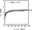
Fig. 3 show for prior art device (reference) and according to device of the present invention (TEOF) as the current density that applies the function of voltage.
Fig. 4 shows for having unmodified PEDOT: the prior art device of PSSA resilient coating is as the efficient of the function of current density.
Fig. 5 shows that for the efficient of device according to the present invention as the function of current density, this device has the PEDOT with triethyl orthoformate (TEOF) esterification of dilution: the PSSA resilient coating.
Fig. 6 shows that for the efficient of device according to the present invention as the function of current density, this device has the PEDOT with the TEOF esterification: the PSSA resilient coating.
Embodiment
In bringing research work of the present invention, produced a kind of neodoxy, promptly in luminescent device, made luminescent layer avoid the influence of the acidity of adjacent buffer layer.
More specifically, invented a kind of method of in polymer LED (PLED), protecting light emitting polymer to avoid the acidic-group influence of resilient coating.
Basic, luminescent device comprises and is clipped in two electric contacting layers luminescent layer between anode and the negative electrode just.Resilient coating is arranged between described luminescent layer and the anode so that increase from injecting and make anode surface smooth in the hole of anode.
Resilient coating, the part that it may also be referred to as hole transmission layer, hole injection layer or bilayer anode comprises conducting polymer and polymeric acid.
The example of conducting polymer is that for example poly-(ethylidene dioxy thiophene) (PEDOT) and polythiofuran derivative for polyaniline (PANi), poly-dioxy thiophene class.
The example of polymeric acid is that poly-(styrene sulfonic acid) (PSSA) (poly (acrylamidoalkylsulphonic acids) (as poly-(acrylamido-2-methyl isophthalic acid-propane sulfonic acid) (PAAMPSA) with poly-(acrylamide alkyl sulfonic acids).Other example of polymeric acid is carbonic acid class and the phosphonic acid based that has the proton of catching by modification according to the present invention equally.
The polymer of described conduction and polymeric acid form polymeric dispersions in water.The example that can be used as the polymeric blends of resilient coating of the present invention is: PEDOT/PSSA, PEDOT/PAAMPSA, PANi/PSSA and PANi/PAAMPSA.
Conducting polymer: the weight ratio of polymeric acid can be for example in 1: 1 to 1: 20 scope or in 1: 3 to 1: 8 scope.For example the weight ratio of PEDOT: PSSA can be 1: 6.
In polymer LED, conducting polymer: the weight ratio of polymeric acid is usually in 1: 6 to 1: 20 scope.
As used herein, term " luminescent layer " relates to a kind of like this layer, and it can be luminous when just anode and negative electrode apply enough bias voltages to electric contacting layer.
Described luminescent layer can for example comprise polymeric material.Light-emitting diode (LED) with the luminescent layer that comprises polymeric material is called polymer LED (PLED).
The preferred polymeric material that is used for according to luminescent layer of the present invention is a NK329 blue light-emitting material, and its structure is presented in the following formula (II):

(k=0.1,m=0.5,n=0.4)
Perhaps, luminescent layer can include organic electro luminescent compounds (emitter), for example organic molecule emitter, oligomeric emitter or dendroid emitter (dendrimeric emitter).
LED with the luminescent layer that comprises organic small molecule material is called OLED.
As shown in Figure 1, there is the enrichment of acidic-group towards the part of luminescent layer at resilient coating.Shown in the specific embodiment, acidic-group is a sulfonic acid group, resilient coating is PEDOT/PSSA, and luminescent layer is light emitting polymer (LEP).
The inventor has been surprised to find that and has protected luminescent layer to avoid the technical feasible method of acidic-group influence very much.More specifically, the inventor suggestion acidic-group that will be enriched in the interface zone between resilient coating and the luminescent layer is converted into nonacid group.And the result reduces to minimum with the quencher that acid causes, and has realized the raising of device efficiency.The example of this conversion is presented among Fig. 2.
As used herein, term " acidic-group " relates in resilient coating or hole injection layer the functional group that the electroluminescent properties of the material that produces light is had negative effect.These groups can be by changing described acid functionality's chemical reaction modification.
As used herein, term " nonacid group " relates to the acid functionality who is modified behind the chemical reaction, and its protection luminescent layer is avoided the negative effect of resilient coating or hole injection layer.
Acidic-group is implemented towards the part of luminescent layer at resilient coating suitably to the described conversion of nonacid group.Therefore, in luminescent layer that part of, will not have acidic-group basically, in anode that part of, then have acidic-group at resilient coating at resilient coating.Yet, all acidic-groups in the resilient coating can be converted into nonacid group.Can before or after applying luminescent layer, transform described acidic-group.
As used herein, term " described resilient coating is towards the part of described luminescent layer " is meant in the device of finishing and the contacted buffer layer part of luminescent layer.
A kind of method that acidic-group is converted into nonacid group is with esterifying agent esterification acidic-group.As used herein, term " esterifying agent " thereby relate to has acid is converted into the chemical reagent that the ester degree of functionality is eliminated the ability of pKa or acidic character.
For example, during as the polymeric acid in the resilient coating, acidic-group is a sulfonic acid group with PSSA, can by adopt have general formula (I) orthoformate and change it non-acid sulfonic acid group of esterification into:

Wherein identical or different R
1, R
2And R
3Be selected from linearity, branching or cyclic alkyl group with 1 to 20 carbon atom, wherein, non-conterminous one or more CH in the described alkyl group
2-group randomly by-O-,-S-,-P-,-Si-,-CO-,-COO-,-O-CO-,-the N-alkyl-,-the N-aryl-or-CON-alkyl-replacement, and one or more H-atom is randomly replaced by CN, Cl, F or aromatic yl group.
According to the present invention, preferred orthoformate is R wherein
1, R
2And R
3Be H
2C-CH
3, promptly the compound of formula (I) is a triethyl orthoformate.Other orthoformate according to formula (I) comprises: orthoformic acid three isopropyl esters, trimethyl orthoformate, orthoformic acid three (octadecyl) ester (trioctadecylorthoformate), tripropyl orthoformate, three (methyl mercapto) methane orthoformate (tris (methylthio) methane orthoformate), three (thiophenyl) methane orthoformate, tributyl orthoformate, triphenyl orthoformate and triethyl orthoformate (all can obtain from Aldrich).Also can adopt the derivative of orthoformate.
Described esterifying agent can use separately, perhaps can be with organic solvent dilution with toluene for example.
(III) set forth the esterification that utilizes triethyl orthoformate by following reaction scheme, and sulfonic acid group is to the conversion as the sulphonic acid ester of the nonacid sulfonic acid group after the esterification:
The advantage of said method is the accessory substance formic acid esters of esterification or is volatile under the working condition that is adopted, perhaps can easily remove by the resilient coating that utilizes suitable solvent washing modification.Also there is other method that can be used for acidic-group is converted into nonacid group.
Provide some examples below:

Chemistry and Industry 1987,857
The Chemistry of sulphonic acids esters and their derivatives,Wiley,New York,1991,pp 351-400
R-SO
2Cl+R′NH
2→R-SO
2NHR′
R-SO
3H+R′R″CN
2→R-SO
3GHR′R″
Synthesis 1984,1041

J.Comb.Chem.2003,5,138
Usually also comprising according to device of the present invention can be in abutting connection with the substrate of described male or female.Modal is substrate and anode adjacency.Described substrate can be pliable and tough or rigidity, organic or inorganic.Usually glass or pliable and tough organic membrane are used as holder.
Described inorganic anode is to injecting or the effective especially electrode of collection positive charge carrier.This anode can be metal, hybrid metal, alloy, metal oxide or mixed-metal oxides.The example of the anode material that is fit to is indium tin oxide (ITO), or other transparent conductive oxide ZnO for example, or as the thin transparent metal layer of Al, Ag or Pt.
Described negative electrode is to injecting or collection electronics or the effective especially electrode of negative charge carrier.This negative electrode can be to have any metal of the work content lower than anode or nonmetal.The example of the cathode material that is fit to is aluminium, calcium, barium, magnesium, silver and zinc selenide (it is transparent and conduction), and their combination or lamination.Described negative electrode can comprise for example lithium fluoride (LiF) etc. of implanted layer extraly.
To one of ordinary skill in the art it is evident that in luminescent device according to the present invention, can also comprise other the layer.In addition, any one can be formed by two or more layers in the above-mentioned layer.In addition, some layers can carry out surface treatment to improve the efficiency of transmission of charge carrier.
Can come fabricate devices by in the substrate that is fit to, depositing each layer in order.In most of the cases, in substrate, apply anode, begin to make up each layer then from here.Usually, different layers will have following thickness range: inorganic anode, 5~500nm, preferred 100~200nm (metal level should enough approach so that be transparent, just in the scope of 5~20nm); Resilient coating, 5~250nm, preferred 20~200nm; Luminescent layer, 1~100nm, preferred 60~100nm; Cathode layer, 20~1000nm, preferred 30~500nm.
Usually adopt vacuum deposition method to apply described inorganic anode layer.
Can adopt any conventional method that comprises spin coating, cast and printing to apply described luminescent layer by solution.According to the character of material, can adopt vapour deposition process directly to apply described luminescent layer.Can also apply the living polymer precursor, be polymer by thermal conversion typically then.
Can adopt any conventional method that comprises spin coating, cast and print for example intaglio printing to apply described resilient coating.Can also apply described resilient coating by ink jet printing.
Usually adopt physical vaporous deposition to apply described cathode layer.
The conversion of resilient coating acidic-group is to realize easily technically, and for example can be by following described enforcement:
-spin coating/ink jet printing is also toasted described resilient coating, for example from the PEDOT of the preferred 1-2% aqueous solution of 0.5%-3%: PSS.Under the temperature more than 100 ℃, toast, preferred more than 180 ℃.
-spin coating/ink jet printing esterifying agent, liquid triethyl orthoformate for example can be with toluene or selectable solvent dilution.
-toast lamination at elevated temperatures, esterification takes place thus, preferably between 50 to 250 ℃, more preferably between 100 to 225 ℃, and most preferably between 180 to 210 ℃.
-with organic solvent for example toluene or dimethylbenzene, chlorinated solvent or insoluble any other orthogonal solvents (orthogonal solvent) spin coating/ink jet printing light emitting polymer of separating following PEDOT/PSSA layer.
Said method also is applicable to other esterifying agent.
Embodiment:
NK329 is adopted standard schedule and produced with standard materials luminescent device as the coloured light polymer that turns blue.The structure that shows NK329 blue light-emitting material in the general formula below (III).

(k=0.1,m=0.5,n=0.4)
Resilient coating is compared with device and the reference device that triethyl orthoformate was handled.
With pure triethyl orthoformate with the triethyl orthoformate of dilution with toluene (3: 1 TEOF: toluene) as esterifying agent.Handle and characterizing device.Esterification does not change the thickness of resilient coating, does not influence current density (referring to Fig. 3) yet.Yet, improved efficient (referring to Fig. 4 to 6 and table 1) as the result of esterification.
Table 1: the blue led efficient that the resilient coating of each modification shows
| Type | Average efficiency (cd/A) | Improve (%) |
| Reference | 2.20 | 0 |
| The TEOF of dilution | 2.35 | 7 |
| Undiluted TEOF | 2.75 | 25 |
Top test data shows, adopts technical feasible simple process step the efficient of this blue light-emitting polymer can be improved 25% by the present invention.
Claims (24)
1. luminescent device comprises:
-anode;
-negative electrode;
-be arranged on the luminescent layer between described anode and the described negative electrode;
-be arranged on the resilient coating that comprises conducting polymer and polymeric acid between described anode and the described luminescent layer;
It is characterized in that, changed nonacid group at acidic-group to polymeric acid described in the described resilient coating of small part.
2. according to the luminescent device of claim 1, wherein described nonacid group is arranged on described resilient coating among the part of described luminescent layer.
3. according to the luminescent device of claim 1 or 2, wherein said nonacid group is transformed by the esterification of acidic-group by esterifying agent.
4. according to the luminescent device of claim 3, wherein said esterifying agent is the orthoformate with general formula (I):

Wherein identical or different R
1, R
2And R
3Be selected from linearity, branching or cyclic alkyl group with 1 to 20 carbon atom, wherein, non-conterminous one or more CH in the described alkyl group
2-group randomly by-O-,-S-,-P-,-Si-,-CO-,-COO-,-O-CO-,-the N-alkyl-,-the N-aryl-or-CON-alkyl-replacement, and one or more H-atom is randomly replaced by CN, Cl, F or aromatic yl group.
5. according to the luminescent device of claim 4, wherein said esterifying agent is a triethyl orthoformate.
6. according to each luminescent device in the aforementioned claim, wherein said nonacid group is the sulfonic acid group of esterification, and described acidic-group is a sulfonic acid group.
7. according to each luminescent device in the aforementioned claim, wherein said resilient coating comprises PEDOT: PSSA.
8. according to each luminescent device in the aforementioned claim, wherein said luminescent layer comprises light emitting polymer.
9. luminescent device according to Claim 8, it is polymer LED (PLED).
10. according to each luminescent device in the claim 1 to 7, wherein said luminescent layer comprises luminous organic molecule.
11. according to the luminescent device of claim 10, it is Organic Light Emitting Diode (OLED).
12. be used to prepare the method for luminescent device, comprise:
-anode is provided;
-negative electrode is provided;
-between described anode and described negative electrode, luminescent layer is set;
-setting comprises the resilient coating of conducting polymer and polymeric acid between described anode and described luminescent layer; And
-in described resilient coating, implement of the conversion of the acidic-group of described polymeric acid to nonacid group to small part.
13., wherein in the part of described luminescent layer, implement of the described conversion of the acidic-group of described polymeric acid to nonacid group at described resilient coating according to the method for claim 12.
14., wherein before on the surface that described luminescent layer is arranged on described resilient coating, on described surface, implement of the described conversion of the acidic-group of described polymeric acid to nonacid group according to the method for claim 12.
15., wherein implement described conversion by the esterification of esterifying agent according to each method in the claim 12 to 14.
16. according to the method for claim 15, wherein by with described esterifying agent spin coating or ink jet printing to described resilient coating, the described acidic-group of esterification is implemented described esterification then.
17. according to the method for claim 16, wherein said esterifying agent is the orthoformate with general formula (I):
Wherein identical or different R
1, R
2And R
3Be selected from linearity, branching or cyclic alkyl group with 1 to 20 carbon atom, wherein, non-conterminous one or more CH in the described alkyl group
2-group randomly by-O-,-S-,-P-,-Si-,-CO-,-COO-,-O-CO-,-the N-alkyl-,-the N-aryl-or-CON-alkyl-replacement, and one or more H-atom is randomly replaced by CN, Cl, F or aromatic yl group.
18. according to the method for claim 17, wherein said esterifying agent is a triethyl orthoformate.
19. according to each method in the claim 12 to 18, wherein said nonacid group is the sulfonic acid group of esterification, and described acidic-group is a sulfonic acid group.
20. according to each method in the claim 12 to 19, wherein said resilient coating comprises PEDOT: PSSA.
21. according to each method in the claim 12 to 20, wherein said luminescent layer comprises light emitting polymer.
22. according to the method for claim 21, wherein said luminescent device is polymer LED (PLED).
23. according to each method in the claim 12 to 20, wherein said luminescent layer comprises luminous organic molecule.
24. according to the luminescent device of claim 23, it is Organic Light Emitting Diode (OLED).
Applications Claiming Priority (2)
| Application Number | Priority Date | Filing Date | Title |
|---|---|---|---|
| EP05108451 | 2005-09-15 | ||
| EP05108451.5 | 2005-09-15 |
Publications (1)
| Publication Number | Publication Date |
|---|---|
| CN101263617A true CN101263617A (en) | 2008-09-10 |
Family
ID=37865335
Family Applications (1)
| Application Number | Title | Priority Date | Filing Date |
|---|---|---|---|
| CNA200680033869XA Pending CN101263617A (en) | 2005-09-15 | 2006-09-08 | Light-emitting device, and method for the manufacture thereof |
Country Status (7)
| Country | Link |
|---|---|
| US (1) | US20080220288A1 (en) |
| EP (1) | EP1927145A2 (en) |
| JP (1) | JP2009509323A (en) |
| KR (1) | KR20080059201A (en) |
| CN (1) | CN101263617A (en) |
| TW (1) | TW200717893A (en) |
| WO (1) | WO2007031923A2 (en) |
Cited By (1)
| Publication number | Priority date | Publication date | Assignee | Title |
|---|---|---|---|---|
| CN113964282A (en) * | 2020-07-20 | 2022-01-21 | Tcl科技集团股份有限公司 | Hole functional layer film and preparation method thereof, and light-emitting diode and preparation method thereof |
Families Citing this family (18)
| Publication number | Priority date | Publication date | Assignee | Title |
|---|---|---|---|---|
| CA2592055A1 (en) | 2004-12-27 | 2006-07-06 | Quantum Paper, Inc. | Addressable and printable emissive display |
| US9425357B2 (en) | 2007-05-31 | 2016-08-23 | Nthdegree Technologies Worldwide Inc. | Diode for a printable composition |
| US8889216B2 (en) | 2007-05-31 | 2014-11-18 | Nthdegree Technologies Worldwide Inc | Method of manufacturing addressable and static electronic displays |
| US8133768B2 (en) | 2007-05-31 | 2012-03-13 | Nthdegree Technologies Worldwide Inc | Method of manufacturing a light emitting, photovoltaic or other electronic apparatus and system |
| US8456393B2 (en) | 2007-05-31 | 2013-06-04 | Nthdegree Technologies Worldwide Inc | Method of manufacturing a light emitting, photovoltaic or other electronic apparatus and system |
| US8846457B2 (en) | 2007-05-31 | 2014-09-30 | Nthdegree Technologies Worldwide Inc | Printable composition of a liquid or gel suspension of diodes |
| US9018833B2 (en) | 2007-05-31 | 2015-04-28 | Nthdegree Technologies Worldwide Inc | Apparatus with light emitting or absorbing diodes |
| US8809126B2 (en) | 2007-05-31 | 2014-08-19 | Nthdegree Technologies Worldwide Inc | Printable composition of a liquid or gel suspension of diodes |
| US9419179B2 (en) | 2007-05-31 | 2016-08-16 | Nthdegree Technologies Worldwide Inc | Diode for a printable composition |
| US8852467B2 (en) | 2007-05-31 | 2014-10-07 | Nthdegree Technologies Worldwide Inc | Method of manufacturing a printable composition of a liquid or gel suspension of diodes |
| US8877101B2 (en) | 2007-05-31 | 2014-11-04 | Nthdegree Technologies Worldwide Inc | Method of manufacturing a light emitting, power generating or other electronic apparatus |
| US8415879B2 (en) | 2007-05-31 | 2013-04-09 | Nthdegree Technologies Worldwide Inc | Diode for a printable composition |
| US8674593B2 (en) | 2007-05-31 | 2014-03-18 | Nthdegree Technologies Worldwide Inc | Diode for a printable composition |
| US9343593B2 (en) | 2007-05-31 | 2016-05-17 | Nthdegree Technologies Worldwide Inc | Printable composition of a liquid or gel suspension of diodes |
| US9534772B2 (en) | 2007-05-31 | 2017-01-03 | Nthdegree Technologies Worldwide Inc | Apparatus with light emitting diodes |
| US7992332B2 (en) | 2008-05-13 | 2011-08-09 | Nthdegree Technologies Worldwide Inc. | Apparatuses for providing power for illumination of a display object |
| US8127477B2 (en) | 2008-05-13 | 2012-03-06 | Nthdegree Technologies Worldwide Inc | Illuminating display systems |
| FR3022079B1 (en) | 2014-06-10 | 2017-08-25 | Commissariat Energie Atomique | ORGANIC ELECTRONIC DEVICE AND METHOD FOR PREPARING THE SAME |
Family Cites Families (5)
| Publication number | Priority date | Publication date | Assignee | Title |
|---|---|---|---|---|
| US6955773B2 (en) * | 2002-02-28 | 2005-10-18 | E.I. Du Pont De Nemours And Company | Polymer buffer layers and their use in light-emitting diodes |
| US20040092700A1 (en) * | 2002-08-23 | 2004-05-13 | Che-Hsiung Hsu | Methods for directly producing stable aqueous dispersions of electrically conducting polyanilines |
| GB0306409D0 (en) | 2003-03-20 | 2003-04-23 | Cambridge Display Tech Ltd | Electroluminescent device |
| JP4381080B2 (en) * | 2003-09-29 | 2009-12-09 | 大日本印刷株式会社 | Organic electroluminescence device and method for producing the same |
| US7351358B2 (en) * | 2004-03-17 | 2008-04-01 | E.I. Du Pont De Nemours And Company | Water dispersible polypyrroles made with polymeric acid colloids for electronics applications |
-
2006
- 2006-09-08 JP JP2008530689A patent/JP2009509323A/en not_active Abandoned
- 2006-09-08 KR KR1020087008865A patent/KR20080059201A/en not_active Application Discontinuation
- 2006-09-08 WO PCT/IB2006/053186 patent/WO2007031923A2/en active Application Filing
- 2006-09-08 US US12/067,049 patent/US20080220288A1/en not_active Abandoned
- 2006-09-08 EP EP06795975A patent/EP1927145A2/en not_active Withdrawn
- 2006-09-08 CN CNA200680033869XA patent/CN101263617A/en active Pending
- 2006-09-12 TW TW095133709A patent/TW200717893A/en unknown
Cited By (1)
| Publication number | Priority date | Publication date | Assignee | Title |
|---|---|---|---|---|
| CN113964282A (en) * | 2020-07-20 | 2022-01-21 | Tcl科技集团股份有限公司 | Hole functional layer film and preparation method thereof, and light-emitting diode and preparation method thereof |
Also Published As
| Publication number | Publication date |
|---|---|
| US20080220288A1 (en) | 2008-09-11 |
| KR20080059201A (en) | 2008-06-26 |
| WO2007031923A2 (en) | 2007-03-22 |
| JP2009509323A (en) | 2009-03-05 |
| WO2007031923A3 (en) | 2007-09-13 |
| TW200717893A (en) | 2007-05-01 |
| EP1927145A2 (en) | 2008-06-04 |
Similar Documents
| Publication | Publication Date | Title |
|---|---|---|
| CN101263617A (en) | Light-emitting device, and method for the manufacture thereof | |
| KR101359205B1 (en) | Polythiophene formulations for improving organic light-emitting diodes | |
| TWI657123B (en) | Perovskite light-emitting device and fabricating method thereof | |
| CN101322259B (en) | Transparent electrode for organic electronic devices | |
| TW200945647A (en) | Organic optoelectronic device and method for manufacturing the same | |
| JP2009509323A5 (en) | ||
| TWI685994B (en) | Organic electroluminescent transistor | |
| US6503643B1 (en) | Electro-luminescent arrangements with thiophene carboxylate metal complexes | |
| TWI421279B (en) | Curable material and its application | |
| CN101009364B (en) | Composition for electron transport layer, electron transport layer manufactured thereof, and organic electroluminescent device including the electron transport layer | |
| WO2011086372A1 (en) | Electro optic devices | |
| CN101501881A (en) | Organic electroluminescence device | |
| US6534200B1 (en) | Electroluminescent systems with polynulcear metal complexes | |
| US20130026457A1 (en) | Polymer blend, organic light-emitting diode including polymer blend, and method of controlling charge mobility of emission layer including polymer blend | |
| CN106796998B (en) | organic electroluminescent transistor | |
| DE102004010811A1 (en) | Composition useful in article of manufacture e.g. electroluminescent arrangement comprises polythiophenes; polymer that is different from polythiophene; and polymer selected from partially fluorinated polymer and/or perfluorinated polymer | |
| ES2303861T3 (en) | ELECTROPHOSPHORESCENT PROVISION WITH CONDUCTIVE POLYMERS. | |
| CN103682132A (en) | Organic light-emitting device and preparation method thereof | |
| Zhang et al. | Triplet-induced degradation: An important consideration in the design of solution-processed hole injection materials for organic light-emitting devices | |
| CN100568579C (en) | Organic light emitting diode | |
| KR101586280B1 (en) | Hole transport high molecular random copolymer and polymer light emitting diode using the Same | |
| KR100581634B1 (en) | High-Efficiency Polymer Electroluminescent Devices with Polymer Insulating Nanolayer | |
| WO2012143109A1 (en) | Fluorinated amines as sam in oleds | |
| Deng et al. | Solution-processed phosphorus-tungsten oxide film as hole injection layer for application in efficient organic light-emitting diode | |
| Zheng et al. | Preparation and performance optimization of TPBISi green-light organic luminescent material devices |
Legal Events
| Date | Code | Title | Description |
|---|---|---|---|
| C06 | Publication | ||
| PB01 | Publication | ||
| C10 | Entry into substantive examination | ||
| SE01 | Entry into force of request for substantive examination | ||
| C02 | Deemed withdrawal of patent application after publication (patent law 2001) | ||
| WD01 | Invention patent application deemed withdrawn after publication |
Open date: 20080910 |