CN101202472B - Rectifier circuit, power supply circuit, and semiconductor device - Google Patents
Rectifier circuit, power supply circuit, and semiconductor device Download PDFInfo
- Publication number
- CN101202472B CN101202472B CN2007101939799A CN200710193979A CN101202472B CN 101202472 B CN101202472 B CN 101202472B CN 2007101939799 A CN2007101939799 A CN 2007101939799A CN 200710193979 A CN200710193979 A CN 200710193979A CN 101202472 B CN101202472 B CN 101202472B
- Authority
- CN
- China
- Prior art keywords
- film
- capacitor
- voltage
- diode
- transistor
- Prior art date
- Legal status (The legal status is an assumption and is not a legal conclusion. Google has not performed a legal analysis and makes no representation as to the accuracy of the status listed.)
- Expired - Fee Related
Links
Images


Classifications
-
- H—ELECTRICITY
- H01—ELECTRIC ELEMENTS
- H01L—SEMICONDUCTOR DEVICES NOT COVERED BY CLASS H10
- H01L27/00—Devices consisting of a plurality of semiconductor or other solid-state components formed in or on a common substrate
- H01L27/02—Devices consisting of a plurality of semiconductor or other solid-state components formed in or on a common substrate including semiconductor components specially adapted for rectifying, oscillating, amplifying or switching and having at least one potential-jump barrier or surface barrier; including integrated passive circuit elements with at least one potential-jump barrier or surface barrier
- H01L27/04—Devices consisting of a plurality of semiconductor or other solid-state components formed in or on a common substrate including semiconductor components specially adapted for rectifying, oscillating, amplifying or switching and having at least one potential-jump barrier or surface barrier; including integrated passive circuit elements with at least one potential-jump barrier or surface barrier the substrate being a semiconductor body
- H01L27/06—Devices consisting of a plurality of semiconductor or other solid-state components formed in or on a common substrate including semiconductor components specially adapted for rectifying, oscillating, amplifying or switching and having at least one potential-jump barrier or surface barrier; including integrated passive circuit elements with at least one potential-jump barrier or surface barrier the substrate being a semiconductor body including a plurality of individual components in a non-repetitive configuration
- H01L27/0611—Devices consisting of a plurality of semiconductor or other solid-state components formed in or on a common substrate including semiconductor components specially adapted for rectifying, oscillating, amplifying or switching and having at least one potential-jump barrier or surface barrier; including integrated passive circuit elements with at least one potential-jump barrier or surface barrier the substrate being a semiconductor body including a plurality of individual components in a non-repetitive configuration integrated circuits having a two-dimensional layout of components without a common active region
- H01L27/0617—Devices consisting of a plurality of semiconductor or other solid-state components formed in or on a common substrate including semiconductor components specially adapted for rectifying, oscillating, amplifying or switching and having at least one potential-jump barrier or surface barrier; including integrated passive circuit elements with at least one potential-jump barrier or surface barrier the substrate being a semiconductor body including a plurality of individual components in a non-repetitive configuration integrated circuits having a two-dimensional layout of components without a common active region comprising components of the field-effect type
- H01L27/0629—Devices consisting of a plurality of semiconductor or other solid-state components formed in or on a common substrate including semiconductor components specially adapted for rectifying, oscillating, amplifying or switching and having at least one potential-jump barrier or surface barrier; including integrated passive circuit elements with at least one potential-jump barrier or surface barrier the substrate being a semiconductor body including a plurality of individual components in a non-repetitive configuration integrated circuits having a two-dimensional layout of components without a common active region comprising components of the field-effect type in combination with diodes, or resistors, or capacitors
-
- H—ELECTRICITY
- H01—ELECTRIC ELEMENTS
- H01L—SEMICONDUCTOR DEVICES NOT COVERED BY CLASS H10
- H01L27/00—Devices consisting of a plurality of semiconductor or other solid-state components formed in or on a common substrate
- H01L27/02—Devices consisting of a plurality of semiconductor or other solid-state components formed in or on a common substrate including semiconductor components specially adapted for rectifying, oscillating, amplifying or switching and having at least one potential-jump barrier or surface barrier; including integrated passive circuit elements with at least one potential-jump barrier or surface barrier
- H01L27/04—Devices consisting of a plurality of semiconductor or other solid-state components formed in or on a common substrate including semiconductor components specially adapted for rectifying, oscillating, amplifying or switching and having at least one potential-jump barrier or surface barrier; including integrated passive circuit elements with at least one potential-jump barrier or surface barrier the substrate being a semiconductor body
- H01L27/08—Devices consisting of a plurality of semiconductor or other solid-state components formed in or on a common substrate including semiconductor components specially adapted for rectifying, oscillating, amplifying or switching and having at least one potential-jump barrier or surface barrier; including integrated passive circuit elements with at least one potential-jump barrier or surface barrier the substrate being a semiconductor body including only semiconductor components of a single kind
- H01L27/0817—Thyristors only
-
- H—ELECTRICITY
- H01—ELECTRIC ELEMENTS
- H01L—SEMICONDUCTOR DEVICES NOT COVERED BY CLASS H10
- H01L27/00—Devices consisting of a plurality of semiconductor or other solid-state components formed in or on a common substrate
- H01L27/02—Devices consisting of a plurality of semiconductor or other solid-state components formed in or on a common substrate including semiconductor components specially adapted for rectifying, oscillating, amplifying or switching and having at least one potential-jump barrier or surface barrier; including integrated passive circuit elements with at least one potential-jump barrier or surface barrier
- H01L27/12—Devices consisting of a plurality of semiconductor or other solid-state components formed in or on a common substrate including semiconductor components specially adapted for rectifying, oscillating, amplifying or switching and having at least one potential-jump barrier or surface barrier; including integrated passive circuit elements with at least one potential-jump barrier or surface barrier the substrate being other than a semiconductor body, e.g. an insulating body
- H01L27/13—Devices consisting of a plurality of semiconductor or other solid-state components formed in or on a common substrate including semiconductor components specially adapted for rectifying, oscillating, amplifying or switching and having at least one potential-jump barrier or surface barrier; including integrated passive circuit elements with at least one potential-jump barrier or surface barrier the substrate being other than a semiconductor body, e.g. an insulating body combined with thin-film or thick-film passive components
Abstract
It is an object of the present invention to provide a rectifier circuit that can suppress deterioration or dielectric breakdown of a semiconductor element due to excessive current. A rectifier circuit of the present invention includes at least a first capacitor, a second capacitor, and a diode which are sequentially connected in series in a path which connects an input terminal and one of two output terminals, and a transistor. The second capacitor is connected between one of a source region and a drain region and a gate electrode of the transistor. Further, the other one of the source region and the drain region and the other one of two output terminals are connected each other.
Description
Technical field
The present invention relates to the power circuit that uses the rectification circuit of diode and use this rectification circuit.The invention still further relates to the semiconductor device that uses above-mentioned rectification circuit or above-mentioned power circuit and can carry out radio communication.
Background technology
And embedding has between the medium (RF label) of integrated circuit and antenna technology with non-contacting mode receiving and transmitting signal (RFID: radio frequency identification) on various fields, obtained actual the use, and be expected to further expand its market as a kind of form of new information communication.The shape that is used for the RF label of RFID under many circumstances is card shape or the more small-sized shaped like chips of ratio card shape, but can adopt various shapes according to its purposes.
In RFID, can utilize electric wave to carry out the communication between reader, read write line or interrogator and the RF label.Particularly, the antenna of electric wave the RF label of launching from interrogator converts the signal of telecommunication into, and the integrated circuit in the RF label is worked according to this signal of telecommunication.And modulated electric wave can send signal to interrogator with non-contacting mode through the signal of telecommunication from antenna emission basis from integrated circuit output.At this, interrogator also has antenna.
Notice that the RF label roughly can divide two types, i.e. active type and passive into.Primary cell is equipped with in active type inside, in the RF label, does not generate electric energy.On the other hand, passive can utilize the electric wave that interrogator launches in the RF label, to generate electric energy.Particularly, at the electric wave that will receive from interrogator after antenna converts alternating voltage into, at rectification circuit to this ac voltage rectifier and use smoothing capacitor etc., thereby be fed in each circuit in the RF label as supply voltage.
In following patent documentation 1, disclose the rectification circuit that uses a diode and smoothing capacitor has been connected to the structure of output one side of this rectification circuit.Structure at 1 disclosed rectification circuit of patent documentation shown in Figure 18 and smoothing capacitor.In rectification circuit shown in Figure 180, diode 800 is connected between input terminal 801 and the lead-out terminal 802.The anode arrangement of diode 800 is in input terminal 801 1 sides, and cathode arrangement is in lead-out terminal 802 1 sides.In addition, one of two electrodes that capacitor 803 is had side is connected to lead-out terminal 802, and the opposing party's ground connection (GND).
No. 2909867 communiques of [patent documentation 1] Japan Patent (the 6th page, the 1st figure)
In RFID, the received-signal strength that comes the regulation interrogator to be launched according to specification or the decree of ISO, JIS etc.
But when the received-signal strength of launching when interrogator was identical, the communication distance between RF label and the interrogator was near more, and the voltage amplitude of the AC signal that antenna received in the RF label is big more.When the voltage amplitude of the AC signal that antenna received is big, by generation voltages higher such as the rectification circuit that receives this signal earlier and smoothing capacitors than desirable value.The voltage that has generated is provided to the circuit of the back level that is connected to this rectification circuit.Its result, owing to the voltage bigger than desirable value is provided to the semiconductor element in this circuit, and the electric current that flows through ground beyond expectation is big, and therefore the problem of easy deterioration of semiconductor element or damage takes place.
In addition, comprise that at the electric wave that interrogator is launched the RF label is exposed to the powerful electric wave that surpasses regulation under the situation of the electronic equipment emission undesired radiation beyond situation and the interrogator of noise.In the case, antenna receives the AC signal that surpasses the such big voltage amplitude of preset range.When the voltage amplitude of the AC signal that antenna received is big, generate the voltage higher than desirable value by the rectification circuit that receives this signal earlier.The voltage that has generated is provided to the circuit of the back level that is connected to this rectification circuit.Its result, owing to the voltage bigger than desirable value is provided to the semiconductor element in this circuit, and the electric current that flows through ground beyond expectation is big, and therefore the problem of easy deterioration of semiconductor element or damage takes place.
In addition,, usually carry out following steps: dwindle the size of the integrated circuit that constitutes by semiconductor element through making the semiconductor element miniaturization, can be formed on the integrated circuit quantity that mother is on glass thereby increase in order to reduce the cost of integrated circuit.But the miniaturization of semiconductor element causes its withstand voltage reduction and because of the easy impaired problem of overcurrent RF label.
In addition, the RF label also has following problem, and when the electric wave of promptly launching when interrogator comprised noise, this noise hindered the operate as normal of the circuit in the RF label.
Suppose the input terminal 801 of rectification circuit shown in Figure 180 is imported the AC signal with the characteristic shown in Figure 19 A.In the case, such shown in the dotted line among Figure 19 B, 800 pairs of diodes are input to the AC signal rectification of input terminal 801, and output to lead-out terminal 802.Because capacitor 803 makes the signal smoothingization that outputs to lead-out terminal 802, the signal that therefore in fact has the characteristic shown in the solid line of Figure 19 B is outputed to lead-out terminal 802.
Figure 19 C changed with the time that the mode that improves time scale illustrates the voltage in the lead-out terminal 802 shown in Figure 19 B.Such shown in Figure 19 C, rise and descend though can see periodic voltage, the average voltage in each cycle remains identical on ideal, and the voltage of signals that outputs to lead-out terminal 802 is considered to direct voltage.
But, comprise in the electric wave that interrogator is launched under the situation of noise that noise is also included within through rectification circuit and is connected in the voltage of its smoothing capacitor of exporting side generation.Figure 19 D is illustrated in the time that low-frequency noise is included in the voltage of the lead-out terminal 802 under the situation in the electric wave that interrogator launches to be changed.Such shown in Figure 19 D, noise (low-frequency noise) appears in the form that the mean value of the voltage in each cycle rose and descends with the longer cycle.When the voltage from rectification circuit output comprised the noise shown in Figure 19 D, direct voltage changed according to the time, therefore may produce harmful effect to the circuit working of back level.
In addition, Figure 19 E time that the voltage of the lead-out terminal 802 under the situation that electric wave that interrogator launches comprises high-frequency noise is shown changes.Because the signal shown in Figure 19 A comprises the signal of higher frequency, so the noise (high-frequency noise) that voltage changes suddenly appears in that kind shown in Figure 19 E.Because when the voltage from rectification circuit output comprised the noise shown in Figure 19 E, identical with the situation that low-frequency noise occurs, direct voltage changed according to the time, so may produce harmful effect to the circuit working of back level.
Summary of the invention
In view of the above problems, problem of the present invention is for providing a kind of rectification circuit, wherein, and at rectification circuit or be connected to the deterioration or the damage that can suppress overvoltage and the caused semiconductor element of overcurrent in the circuit of back level of rectification circuit.In addition, a kind of semiconductor device is provided also, wherein, at rectification circuit or be connected in the circuit of back level of rectification circuit and can suppress the deterioration or the damage of overvoltage and the caused semiconductor element of overcurrent, and can carries out radio communication.
In addition, in view of the above problems, problem of the present invention wherein, can prevent that noise is included in the voltage of being exported, and formed by rectification circuit and smoothing capacitor for a kind of power circuit is provided.In addition, a kind of semiconductor device is provided also, wherein, can prevents that also this noise from hindering the operate as normal of integrated circuit even the electric wave that interrogator is launched comprises noise, and wirelessly communicate.
Rectification circuit of the present invention also comprises at least one MOS (metal-oxide semiconductor (MOS)) transistor except existing diode, this MOS transistor has capacitor between either party of gate electrode and source region or drain region.
Specifically, rectification circuit of the present invention has first capacitor, second capacitor, diode at least, they link transistor, input terminal, and two lead-out terminals in the path of either party lead-out terminal on be connected in series in order.Second capacitor is connected between the side and gate electrode in above-mentioned transistorized source region or drain region.In addition, rectification circuit of the present invention has a diode at least.The opposing party in above-mentioned transistorized source region and drain region is connected to the opposing party's lead-out terminal in said two lead-out terminals.Noting, is under the situation of n channel-type at above-mentioned transistor, and either party of this transistorized source region and drain region is connected to the negative electrode of diode.In contrast, be under the situation of p channel-type at this transistor, either party of this transistorized source region and drain region is connected to the anode of diode.Through said structure, when to the input terminal input exchange signal, from two lead-out terminals either party output by rectification signal.
In addition, power circuit of the present invention also has the 3rd capacitor that is parallel-connected between two lead-out terminals except above-mentioned rectification circuit.Through above-mentioned the 3rd capacitor, make from the signal smoothingization of either party output of lead-out terminal, thereby generate direct voltage.
Notice that rectification circuit of the present invention or power circuit also can be connected to resistor or diode between above-mentioned transistorized gate electrode and the lead-out terminal.
In addition, semiconductor device of the present invention has above-mentioned rectification circuit or above-mentioned power circuit in integrated circuit, and the AC signal that antenna received is input to the input terminal of rectification circuit or the input terminal of power circuit.Notice that semiconductor device of the present invention has integrated circuit at least and gets final product, and also can not comprise antenna.Moreover the integrated circuit that semiconductor device of the present invention had has the rectification circuit of the AC signal rectification that antenna is received at least or the power circuit that the voltage commutation of the AC signal that antenna received generates direct voltage is got final product.
In rectification circuit of the present invention, between one of input terminal and lead-out terminal, first capacitor and second capacitor and diode or transistorized prime are connected in series.Therefore, even the big alternating voltage of voltage amplitude is fed to input terminal, also can make the voltage that is applied to transistor and diode less.In addition, diode and transistor are not directly applied voltage.Thereby, can suppress the caused diode of overvoltage and transistorized deterioration or damage.
Therefore, even the communication distance between interrogator and the RF label is short, or, also can guarantee the reliability of semiconductor device because of undesired radiation RF label is exposed to the powerful electric wave that surpasses regulation.
In addition, in power circuit of the present invention, the transistor or the diode that are in on-state can be counted as resistor.Therefore, second capacitor is connected with this resistor in series.In addition, the 3rd capacitor and transistor and diode are connected in parallel.Because this second capacitor, resistor and the 3rd capacitor also play the effect of low pass filter; Even comprise high-frequency noise, can prevent that also this noise is included in the direct voltage that generates through rectification circuit and smmothing capacitor so be fed to the alternating voltage of input terminal.
Moreover; In power circuit of the present invention; When resistor being connected between transistorized gate electrode and the lead-out terminal; Because this resistor and first capacitor play the effect of high pass filter, so comprise low-frequency noise even be fed to the alternating voltage of input terminal, can prevent that also this noise is included in the direct voltage that generates in the power circuit.
Thereby even the electric wave that interrogator is launched comprises high frequency or low-frequency noise, this noise also is not easy to be included in the direct voltage that generates in the power circuit.Its result uses the work of the various circuit in the semiconductor device of this direct voltage work to be not easy to receive The noise, thereby can make the working stability of semiconductor device.
Description of drawings
Figure 1A and 1B are the circuit diagrams that the structure of rectification circuit of the present invention and power circuit is shown;
Fig. 2 A and 2B are the figure that the action of rectification circuit of the present invention and power circuit is shown;
Fig. 3 A and 3B are the figure that the action of rectification circuit of the present invention and power circuit is shown;
Fig. 4 A and 4B are the circuit diagrams that the structure of rectification circuit of the present invention and power circuit is shown;
Fig. 5 A and 5B are the figure that the action of rectification circuit of the present invention and power circuit is shown;
Fig. 6 A and 6B are the figure that the action of rectification circuit of the present invention and power circuit is shown;
Fig. 7 A and 7B are the circuit diagrams that the structure of rectification circuit of the present invention and power circuit is shown;
Fig. 8 is the calcspar that the structure of semiconductor device of the present invention is shown;
Fig. 9 A and 9B are the figure that the outward appearance of semiconductor device of the present invention is shown;
Figure 10 A to 10C is the figure that the manufacturing approach of semiconductor device of the present invention is shown;
Figure 11 A to 11C is the figure that the manufacturing approach of semiconductor device of the present invention is shown;
Figure 12 A and 12B are the figure that the manufacturing approach of semiconductor device of the present invention is shown;
Figure 13 A and 13B are the figure that the manufacturing approach of semiconductor device of the present invention is shown;
Figure 14 A to 14C is the figure that the manufacturing approach of semiconductor device of the present invention is shown;
Figure 15 A to 15C is the figure that the manufacturing approach of semiconductor device of the present invention is shown;
Figure 16 A and 16B are the figure that the manufacturing approach of semiconductor device of the present invention is shown;
Figure 17 is the vertical view of power circuit of the present invention;
Figure 18 is the circuit diagram that the structure of existing rectification circuit is shown;
Figure 19 A to 19E illustrates the figure that changes from the time of the voltage of rectification circuit output;
Figure 20 A and 20B are the figure that utilizes method that semiconductor device of the present invention is shown;
Figure 21 A and 21B are the figure that utilizes method that semiconductor device of the present invention is shown;
Figure 22 is the figure that the structure of the thin-film secondary battery that is used for semiconductor device of the present invention is shown;
Figure 23 is the calcspar that the structure of semiconductor device of the present invention is shown;
Figure 24 is the figure that the action of semiconductor device of the present invention is shown.
Embodiment
Below, will be with reference to description of drawings execution mode of the present invention.But; The present invention can implement through different ways, and the ordinary person of affiliated technical field can understand a fact at an easy rate, and to be exactly its mode and detailed content can be transformed to various forms not breaking away under aim of the present invention and the scope thereof.Therefore, the present invention should not be interpreted as only for fixing in the content that this execution mode puts down in writing.
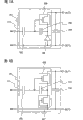
The structure of rectification circuit of the present invention and power circuit is described with reference to Figure 1A and 1B.In Figure 1A, Reference numeral 101 is equivalent to rectification circuit of the present invention.Rectification circuit 101 is connected to two input terminal IN1, IN2 and two lead-out terminal OUT1, OUT2.Two terminals that antenna had are connected respectively to input terminal IN1 and input terminal IN2.In addition, rectification circuit 101 has first capacitor 102, second capacitor 103, diode 105, transistor 106 at least.Notice that Figure 1A is illustrated in the structure of the rectification circuit 101 under the situation that transistor 106 is n channel-types.In addition, power circuit 111 of the present invention also has the 3rd capacitor 104 except rectification circuit 101.
On the path that links input terminal IN1 and lead-out terminal OUT2, first capacitor 102, second capacitor 103, diode 105 are connected in series in order.Illustrate in greater detail, first electrode that first capacitor 102 is had is connected to input terminal IN1.In addition, second electrode that had of first capacitor 102 is connected to first electrode that second capacitor 103 is had.Second electrode that second capacitor 103 is had is connected to the negative electrode of diode 105.The anode of diode 105 is connected to lead-out terminal OUT2 and input terminal IN2.
In addition, first capacitor 102 is connected between the gate electrode of input terminal IN1 and transistor 106.In addition, second capacitor 103 is connected between the gate electrode of a side and transistor 106 in source region and drain region of transistor 106.The source region of transistor 106 and in the drain region either party are connected to lead-out terminal OUT1, and the opposing party is connected to the negative electrode of diode 105.The anode of diode 105 not only is connected to lead-out terminal OUT2, but also is connected to input terminal IN2.The 3rd capacitor 104 is connected between lead-out terminal OUT1 and lead-out terminal OUT2 and the input terminal IN2.
Note, also can resistor or diode be connected between second electrode and lead-out terminal OUT2 that first capacitor 102 had.
In addition, as diode 105, also can use transistor.In the case, diode 105 also can be through forming with transistor 106 identical manufacturing processes.Figure 1B is illustrated in rectification circuit 101 and the power circuit 111 of Figure 1A the structure of n channel transistor 107 as the situation of diode 105.The gate electrode of the transistor 107 of Figure 1B is connected to input terminal IN2 and lead-out terminal OUT2.In addition, the side is connected to second electrode that second capacitor 103 is had one of in the source region of transistor 107 and the drain region, and the opposing party is connected to gate electrode, lead-out terminal OUT2 and input terminal IN2.When regarding n channel transistor 107 as diode, the zone that is connected to gate electrode among source region and the drain region is used as anode with gate electrode, and another zone is as negative electrode.
Notice that transistor 107 also can be the p channel-type.In the case, the gate electrode of transistor 107 is connected to second electrode that second capacitor 103 is had.In addition, the side is connected to input terminal IN2 and lead-out terminal OUT2 one of in the source region of transistor 107 and the drain region, and the opposing party is connected to second electrode that gate electrode and second capacitor 103 are had.When regarding p channel transistor 107 as diode, the zone that is connected to gate electrode among source region and the drain region is used as negative electrode with gate electrode, and another zone is as anode.
The action of rectification circuit 101 shown in Figure 1A and power circuit 111 then, is described with reference to Fig. 2 A.Such shown in Fig. 2 A, suppose the voltage Vh higher than ground connection (GND) is applied to input terminal IN1.At this moment, input terminal IN2 and lead-out terminal OUT2 are connected to ground (GND).When voltage Vh is applied to input terminal IN1, second electrode of first capacitor 102, first electrode of second capacitor 103 and the gate electrode of transistor 106 are applied voltage Vh.Below, the voltmeter of the gate electrode of first electrode of second electrode of first capacitor 102, second capacitor 103 and transistor 106 is shown the voltage of first node (N1).Notice that in fact, because voltage reduces according to gate capacitance, dead resistance and the parasitic capacitance of first capacitor 102, second capacitor 103, transistor 106, so the voltage of first node (N1) is lower than voltage Vh.Even but with the voltage of first node think with voltage Vh much at one, the action explanation on also no problem.
When the voltage of first node (N1) becomes voltage Vh, second electrode of second capacitor 103 and the negative electrode of diode 105 are applied voltage Vh.Below, the voltmeter of the negative electrode of second electrode of second capacitor 103 and diode 105 is shown the voltage of Section Point (N2).Notice that in fact, because voltage reduces according to gate electrode and the electric capacity between the drain region, dead resistance and the parasitic capacitance of second capacitor 103, transistor 106, so the voltage ratio voltage Vh of Section Point (N2) is lower.Even but the voltage of Section Point is thought also no problem in the explanation of action much at one with voltage Vh.
When the voltage of Section Point (N2) becomes voltage Vh; Because transistor 106 is n channel-types; Regard drain region (D) as so be connected to the zone of negative electrode of second electrode and the diode 105 of second capacitor 103 in a pair of extrinsic region that can transistor 106 be had, and can regard the zone that is connected to lead-out terminal OUT1 as source region (S).When the gate voltage that is equivalent to the voltage between gate electrode and the source region became the threshold voltage vt h that is higher than transistor 106, transistor 106 was connected.In addition, because diode 105 is applied back-biased voltage, so diode 105 ends.Thereby voltage, this moment of having reduced the threshold voltage vt h of transistor 106 than the voltage of Section Point (N2) are supplied to lead-out terminal OUT1 for voltage (Vh-Vth).
Fig. 2 B is illustrated in the structure that the transistor that is in on-state 106 is counted as the power circuit 111 under the situation of resistor.Because diode 105 ends in Fig. 2 A, so in Fig. 2 B, it is illustrated as the switch of open circuit.Input terminal IN1 is being applied under the situation of voltage Vh first capacitor 102, second capacitor 103 and be connected in series as the transistor 106 of resistor.The 3rd capacitor 104 is connected between the lead-out terminal OUT2 of lead-out terminal OUT1 and ground connection (GND).Since this second capacitor 103, as the transistor 106 of resistor and the 3rd capacitor 104 as low pass filter 108; Even comprise high-frequency noise, can prevent that also this noise is included in from the direct voltage of lead-out terminal OUT1 output so be fed to the AC signal of input terminal IN1.
Moreover, in power circuit 111 of the present invention, resistor 110 being connected under second electrode and the situation between the second input terminal IN2 that first capacitor 102 had, first capacitor 102 plays high pass filter 109 with this resistor 110.Therefore, comprise that low-frequency noise can prevent that also this noise is included in from the direct voltage of lead-out terminal OUT1 output even be fed to the AC signal of input terminal IN1.
Thereby; Even the electric wave that interrogator is launched comprises high frequency or low-frequency noise; This noise also is not easy to be included in from the direct voltage of power circuit 111 outputs, therefore uses this direct voltage to come the work of the various circuit of work to be not easy to receive this The noise.Thereby can make the working stability of various circuit.
Note, in low pass filter 108, when the frequency through the voltage of this filter is F
L, second capacitor 103 capacitance be that C2, the resistance value under the situation of transistor 106 being regarded as resistor are R
t, the 3rd capacitor 104 capacitance when being C3, F
LSatisfy formula 1.Therefore, preferably set capacitance C2, resistance value R according to the frequency of the noise that will interdict
t, and the value of capacitance C3.In addition, in high pass filter 109, when the frequency through the voltage of this filter is F
H, first electric capacity 102 capacitance be the resistance value of C1, resistor 110 when being R, satisfy F
H>=1/ (2 π * C1 * R).Therefore, preferably set the value of capacitance C1, resistance value R according to the frequency of the noise that will interdict.
[formula 1]
Then, such shown in Fig. 3 A, suppose to input terminal IN1 apply the voltage Vl lower than ground connection (GND) (=-Vh).At this moment, input terminal IN2 ground connection (GND).When input terminal IN1 was applied voltage Vl, the voltage of first node (N1) became voltage Vl.Notice that in fact, because voltage raises according to gate capacitance, dead resistance and the parasitic capacitance of first capacitor 102, second capacitor 103, transistor 106, so the voltage ratio voltage Vl of first node (N1) is high.Even but the voltage of first node is thought also no problem in the explanation of action much at one with voltage Vl.
When the voltage of first node (N1) became voltage Vl, the voltage of Section Point (N2) also became voltage Vl.Notice that in fact, because voltage raises according to gate electrode and the electric capacity between the drain region, dead resistance and the parasitic capacitance of second capacitor 103, transistor 106, so the voltage ratio voltage Vl of Section Point (N2) is higher.Even but the voltage of Section Point is thought also no problem in the explanation of action much at one with voltage Vl.
When the voltage of Section Point (N2) becomes voltage Vl; Because transistor 106 is n channel-types; Regard source region (S) as so be connected to the zone of negative electrode of second electrode and the diode 105 of second capacitor 103 in a pair of extrinsic region that can transistor 106 be had, and can regard the zone that is connected to lead-out terminal OUT1 as drain region (D).When gate voltage was lower than the threshold voltage vt h of transistor 106, transistor 106 ended.At this, the voltage of lead-out terminal OUT1 is kept by the 3rd capacitor 104.In addition, because diode 105 is applied the voltage of forward bias, so diode 105 is connected.Therefore, the voltage of Section Point (N2) becomes the voltage of ground connection (GND) gradually.
Fig. 3 B is illustrated in the structure of the transistor that is in cut-off state 106 being regarded as the power circuit 111 under the situation of switch of open circuit.Because diode 105 is connected in Fig. 3 A, so in Fig. 3 B, it is illustrated as resistor.Such shown in Fig. 3 B, be applied at voltage Vl under the situation of input terminal IN1, first capacitor 102 likewise is used as high pass filter 109 with resistor 110 and the situation shown in Fig. 2 B.Moreover second capacitor 103 and the resistor that formed by diode 105 are as high pass filter 112.Therefore become the structure that the two-stage, high-pass filter is connected in series, be included in from the direct voltage of lead-out terminal OUT1 output thereby low-frequency noise is more difficult.
Notice that the kind and the quantity thereof that are used for the semiconductor element of rectification circuit 101 and power circuit 111 are not limited to the structure shown in this execution mode.Except the semiconductor element shown in Figure 1A, resistor, capacitor, diode, inductor, switch etc. can also suitably be provided, to obtain better rectification characteristic.
Such as stated, in the rectification circuit of this execution mode, first capacitor 102 and second capacitor 103 are connected in series with the prime of diode 105 or transistor 106.Therefore when the AC signal that the amplitude of voltage is big is fed to input terminal IN1, also can make the voltage that is applied to diode 105 or transistor 106 little.In addition, to diode 105 or and transistor 106 directly do not apply voltage.Thereby, can suppress the deterioration or the damage of caused diode 105 of overvoltage or transistor 106.
In addition, in the power circuit 111 of this execution mode, even the electric wave that interrogator is launched comprises high frequency or low-frequency noise, this noise also is not easy to be included in from the direct voltage of power circuit 111 outputs.Its result uses this direct voltage to come the work of the various circuit in the semiconductor device of work to be not easy to receive The noise, thereby can make the working stability of semiconductor device.
Execution mode 2
The structure of rectification circuit of the present invention and power circuit is described with reference to Fig. 4 A and 4B.In Fig. 4 A, Reference numeral 201 is equivalent to rectification circuit of the present invention.Rectification circuit 201 is connected to two input terminal IN1, IN2 and two lead-out terminal OUT1, OUT2.Two terminals that antenna had are connected respectively to input terminal IN1 and input terminal IN2.In addition, rectification circuit 201 has first capacitor 202, second capacitor 203, diode 205, transistor 206 at least.Notice that Fig. 4 A is illustrated in the structure of the rectification circuit 201 under the situation that transistor 206 is p channel-types.In addition, power circuit 211 of the present invention also has the 3rd capacitor 204 except rectification circuit 201.
On the path that links input terminal IN1 and lead-out terminal OUT1, first capacitor 202, second capacitor 203, diode 205 are connected in series in order.Illustrate in greater detail, first electrode that first capacitor 202 is had is connected to input terminal IN1.In addition, second electrode that had of first capacitor 202 is connected to first electrode that second capacitor 203 is had.Second electrode that second capacitor 203 is had is connected to the anode of diode 205.The negative electrode of diode 205 is connected to lead-out terminal OUT1.
Note, also can resistor or diode be connected between second electrode and lead-out terminal OUT2 that first capacitor 202 had.
In addition, as diode 205, also can use transistor.In the case, diode 205 also can be through forming with transistor 206 identical manufacturing processes.Fig. 4 B is illustrated in rectification circuit 201 and the power circuit 211 of Fig. 4 A the structure of p channel transistor 207 as the situation of diode 205.In the transistor 207 of Fig. 4 B, gate electrode is connected to lead-out terminal OUT2.In addition, the side is connected to second electrode that second capacitor 203 is had one of in the source region of transistor 207 and the drain region, and the opposing party is connected to gate electrode and lead-out terminal OUT1.When regarding p channel transistor 207 as diode, the zone that is connected to gate electrode among source region and the drain region is used as negative electrode with gate electrode, and another zone is as anode.
Notice that transistor 207 also can be the n channel-type.In the case, the gate electrode of transistor 207 is connected to second electrode that second capacitor 203 is had.In addition, the side is connected to second electrode that second capacitor 203 is had with gate electrode one of in the source region of transistor 207 and the drain region, and the opposing party is connected to lead-out terminal OUT1.When regarding n channel transistor 207 as diode, the zone that is connected to gate electrode among source region and the drain region is used as anode with gate electrode, and another zone is as negative electrode.
The action of rectification circuit 201 shown in Fig. 4 A and power circuit 211 then, is described with reference to Fig. 5 A.Such shown in Fig. 5 A, suppose the voltage Vh higher than ground connection (GND) is applied to input terminal IN1.At this moment, input terminal IN2 is connected to ground connection (GND).When voltage Vh is applied to input terminal IN1, second electrode of first capacitor 202, first electrode of second capacitor 203 and the gate electrode of transistor 206 are applied voltage Vh.Below, the voltmeter of the gate electrode of first electrode of second electrode of first capacitor 202, second capacitor 203 and transistor 206 is shown the voltage of first node (N1).Notice that in fact, because voltage reduces according to gate capacitance, dead resistance and the parasitic capacitance of first capacitor 202, second capacitor 203, transistor 206, so the voltage of first node (N1) is lower than voltage Vh.Even but with the voltage of first node think with voltage Vh much at one, the action explanation on also no problem.
When the voltage of first node (N1) becomes voltage Vh, second electrode of second capacitor 203 and the anode of diode 205 are applied voltage Vh.Below, the voltmeter of the anode of second electrode of second capacitor 203 and diode 205 is shown the voltage of Section Point (N2).Notice that in fact, because voltage reduces according to gate electrode and the electric capacity between the drain region, dead resistance and the parasitic capacitance of second capacitor 203, transistor 206, so the voltage ratio voltage Vh of Section Point (N2) is lower.Even but the voltage of Section Point is thought also no problem in the explanation of action much at one with voltage Vh.
When the voltage of Section Point (N2) becomes voltage Vh; Because transistor 206 is p channel-types; Regard source region (S) as so be connected to the zone of anode of second electrode and the diode 205 of second capacitor 203 in a pair of extrinsic region that can transistor 206 be had, and can regard the zone that is connected to lead-out terminal OUT2 as drain region (D).When the gate voltage that is equivalent to the voltage between gate electrode and the source region became the threshold voltage vt h that is higher than transistor 206, transistor 206 ended.In addition, owing to the voltage that diode 205 is applied forward bias, so diode 205 is connected.Thereby deduct the voltage Vd that diode 205, reduces and the voltage that obtains, this moment are fed to lead-out terminal OUT1 for voltage (Vh-Vd), and the voltage of the 3rd capacitor 204 maintenance lead-out terminal OUT1 from the voltage of Section Point (N2).
Fig. 5 B is illustrated in the structure of the diode that is in on-state 205 being regarded as the power circuit 211 under the situation of resistor.Transistor 206 ends in Fig. 5 A, and in Fig. 5 B, it is illustrated as the switch of open circuit.Input terminal IN1 is being applied under the situation of voltage Vh first capacitor 202, second capacitor 203 and be connected in series as the diode 205 of resistor.The 3rd capacitor 204 is connected between the lead-out terminal OUT2 of lead-out terminal OUT1 and ground connection (GND).Since this second capacitor 203, as the diode 205 of resistor and the 3rd capacitor 204 as low pass filter 208; Even comprise high-frequency noise, can prevent that also this noise is included in from the direct voltage of lead-out terminal OUT1 output so be fed to the AC signal of input terminal IN1.
Moreover, in power circuit 211 of the present invention, resistor 210 being connected under second electrode and the situation between the second input terminal IN2 that first capacitor 202 had, first capacitor 202 and this resistor 210 are as high pass filter 209.Therefore, comprise that low-frequency noise can prevent that also this noise is included in from the direct voltage of lead-out terminal OUT1 output even be fed to the alternating voltage of input terminal IN1.
Therefore, even the electric wave that interrogator is launched comprises high frequency or low-frequency noise, this noise also is not easy to be included in from the direct voltage of rectification circuit 201 outputs, thereby this noise is not easy to hinder the work of using this direct voltage to come the various circuit of work.
Note, in low pass filter 208, when the frequency through the voltage of this filter is F
L, second capacitor 203 capacitance be that C2, the resistance value under the situation of diode 205 being regarded as resistance are R
t, the 3rd capacitor 204 capacitance when being C3, F
LSatisfy formula 1.Therefore, preferably set the value of capacitance C2, resistance value Rt and capacitance C3 according to the frequency of the noise that will interdict.In addition, in high pass filter 209, when the frequency through the voltage of this filter is F
H, first capacitor 202 capacitance be the resistance value of C1, resistor 210 when being R, satisfy F
H>=1/ (2 π * C1 * R).Therefore, preferably set the value of capacitance C1, resistance value R according to the frequency of the noise that will interdict.
Then, such shown in Fig. 6 A, suppose to input terminal IN1 apply the voltage Vl lower than ground connection (GND) (=-Vh).At this moment, input terminal IN2 is connected to ground connection (GND).When input terminal IN1 was applied voltage Vl, the voltage of first node (N1) became voltage Vl.Notice that in fact, because voltage raises according to gate capacitance, parasitic capacitance and the dead resistance of first capacitor 202, second capacitor 203, transistor 206, so the voltage ratio voltage Vl of first node (N1) is high.Even but the voltage of first node is thought also no problem in the explanation of action much at one with voltage Vl.
When the voltage of first node (N1) became voltage Vl, the voltage of Section Point (N2) also became voltage Vl.Notice that in fact, because voltage raises according to gate electrode and the electric capacity between the source region, dead resistance and the parasitic capacitance of second capacitor 203, transistor 206, so the voltage ratio voltage Vl of Section Point (N2) is higher.Even but the voltage of Section Point is thought also no problem in the explanation of action much at one with voltage Vl.
When the voltage of Section Point (N2) becomes voltage Vl; Because transistor 206 is p channel-types; Regard drain region (D) as so be connected to the zone of anode of second electrode and the diode 205 of second capacitor 203 in a pair of extrinsic region that can transistor 206 be had, and can regard the zone that is connected to lead-out terminal OUT2 as source region (S).When the gate voltage that is equivalent to the voltage between gate electrode and the source region was lower than the threshold voltage vt h of transistor 206, transistor 206 was connected.In addition, because diode 205 is applied the voltage of reverse biased, so diode 205 ends.Therefore, the voltage of Section Point (N2) becomes the voltage of ground connection (GND) gradually.The 3rd capacitor 204 keeps the voltage of lead-out terminal OUT1.
Fig. 6 B is illustrated in the structure of the diode that is in cut-off state 205 being regarded as the power circuit 211 under the situation of switch of open circuit.Because transistor 206 is connected in Fig. 6 A, so in Fig. 6 B, it is illustrated as resistor.Such shown in Fig. 6 B, be applied at voltage Vl under the situation of input terminal IN1, first capacitor 202 likewise is used as high pass filter 209 with resistor 210 and the situation shown in Fig. 5 B.Moreover second capacitor 203 and the resistor that formed by transistor 206 are as high pass filter 212.Therefore become the structure that the two-stage, high-pass filter is connected in series, be included in from the direct voltage of lead-out terminal OUT1 output thereby low-frequency noise is more difficult.
Notice that the kind and the quantity thereof that are used for the semiconductor element of rectification circuit 201 and power circuit 211 are not limited to the structure shown in this execution mode.Except the semiconductor element shown in Fig. 4 A, resistor, capacitor, diode, inductor, switch etc. can also suitably be provided, to obtain better rectification characteristic.
Such as stated, in the rectification circuit of this execution mode, first capacitor 202 and second capacitor 203 are connected in series with the prime of diode 205 or transistor 206.Therefore when the AC signal that the amplitude of voltage is big is fed to input terminal IN1, also can make the voltage that is applied to diode 205 or transistor 206 little.In addition, diode 205 or transistor 206 are not directly applied voltage.Thereby, can suppress the deterioration or the damage of caused diode 205 of overvoltage or transistor 206.
In addition, in this execution mode, even the electric wave that interrogator is launched comprises high frequency or low-frequency noise, this noise also is not easy to be included in from the direct voltage of power circuit 211 outputs.Its result uses this direct voltage to come the work of the various circuit in the semiconductor device of work to be not easy to receive The noise, thereby can make the working stability of semiconductor device.
Execution mode 3
In execution mode 1 and 2, explained and to have obtained the rectification circuit of positive direct voltage and the structure of power circuit from lead-out terminal OUT1.In this execution mode, the rectification circuit of the present invention of the direct voltage that explanation can obtain to bear and the structure of power circuit.
Fig. 7 A illustrates the structure of the rectification circuit and the power circuit of this execution mode.Rectification circuit 301 shown in Fig. 7 A is connected to two input terminal IN1, IN2 and two lead-out terminal OUT1, OUT2.Two terminals that antenna had are connected respectively to input terminal IN1 and input terminal IN2.In addition, rectification circuit 301 has first capacitor 302, second capacitor 303, diode 305, transistor 306 at least.Notice that Fig. 7 A illustrates the structure of the rectification circuit 301 under the situation that transistor 306 is n channel-types.In addition, power circuit 309 of the present invention also has the 3rd capacitor 304 except rectification circuit 301.
On the path that links input terminal IN1 and lead-out terminal OUT1, first capacitor 302, second capacitor 303, diode 305 are connected in series in order.Illustrate in greater detail, first electrode that first capacitor 302 is had is connected to input terminal IN1.In addition, second electrode that had of first capacitor 302 is connected to first electrode that second capacitor 303 is had.Second electrode that second capacitor 303 is had is connected to the negative electrode of diode 305.The anode of diode 305 is connected to lead-out terminal OUT1.
In addition, first capacitor 302 is connected between the gate electrode of input terminal IN1 and transistor 306.Moreover second capacitor 303 is connected between the gate electrode of a side and transistor 306 in source region and drain region of transistor 306.The source region of transistor 306 and in the drain region either party are connected to input terminal IN2 and lead-out terminal OUT2, and the opposing party is connected to the negative electrode of diode 305.The 3rd capacitor 304 is connected between lead-out terminal OUT1 and the lead-out terminal OUT2.
Note, also can resistor or diode be connected between second electrode and lead-out terminal OUT2 that first capacitor 302 had.
In addition, as diode 305, also can use transistor.In the case, diode 305 also can be through forming with transistor 306 identical manufacturing processes.Using under the situation of n channel transistor as diode 305, this transistorized gate electrode is connected to lead-out terminal OUT1.In addition, just be connected to second electrode that second capacitor 303 is had as the transistorized source region of diode 305 and one of drain region, the opposing party is connected to gate electrode and lead-out terminal OUT1.When regarding the n channel transistor as diode, the zone that is connected to gate electrode among source region and the drain region is used as anode with gate electrode, and another zone is as negative electrode.In addition, using under the situation of p channel transistor as diode 305, this transistorized gate electrode is connected to second electrode that second capacitor 303 is had.In addition, the side is connected to lead-out terminal OUT1 as one of the transistorized source region of diode 305 and drain region, and the opposing party is connected to second electrode that gate electrode and second capacitor 303 are had.When regarding the p channel transistor as diode, the zone that is connected to gate electrode among source region and the drain region is used as negative electrode with gate electrode, and another zone is as anode.
Through said structure, when to input terminal IN1 input exchange signal, from the negative direct voltage of lead-out terminal OUT1 output.
Notice that the kind and the quantity thereof that are used for the semiconductor element of rectification circuit 301 and power circuit 309 are not limited to the structure shown in this execution mode.Except the semiconductor element shown in Fig. 7 A, resistor, capacitor, diode, inductor, switch etc. can also suitably be provided, to obtain better rectification characteristic.
In the rectification circuit shown in Fig. 7 A, first capacitor 302 and second capacitor 303 are connected in series with the prime of diode 305 or transistor 306.Therefore when the AC signal that the amplitude of voltage is big is fed to input terminal IN1, also can make the voltage that is applied to diode 305 or transistor 306 little.In addition, diode 305 or transistor 306 are not directly applied voltage.Thereby, can suppress the deterioration or the damage of caused diode 305 of overvoltage or transistor 306.
In addition, identical with the situation of the rectification circuit shown in Figure 1A in the power circuit shown in Fig. 7 A 309, even the electric wave that interrogator is launched comprises high frequency or low-frequency noise, this noise also is not easy to be included in from the direct voltage of power circuit 309 outputs.Its result uses this direct voltage to come the work of the various circuit in the semiconductor device of work to be not easy to receive The noise, thereby can make the working stability of semiconductor device.
Below, the rectification circuit of the present invention of the direct voltage that explanation can obtain to bear and other structures of power circuit.
Fig. 7 B illustrates the structure of the rectification circuit and the power circuit of this execution mode.Rectification circuit 311 shown in Fig. 7 B is connected to two input terminal IN1, IN2 and two lead-out terminal OUT1, OUT2.Two terminals that antenna had are connected respectively to input terminal IN1 and input terminal IN2.In addition, rectification circuit 311 has first capacitor 312, second capacitor 313, diode 315, transistor 316 at least.Notice that Fig. 7 B illustrates the structure of the rectification circuit 311 under the situation that transistor 316 is p channel-types.In addition, power circuit 319 of the present invention also has the 3rd capacitor 314 except rectification circuit 311.
On the path that links input terminal IN1 and lead-out terminal OUT2, first capacitor 312, second capacitor 313, diode 315 are connected in series in order.Illustrate in greater detail, first electrode that first capacitor 312 is had is connected to input terminal IN1.In addition, second electrode that had of first capacitor 312 is connected to first electrode that second capacitor 313 is had.Second electrode that second capacitor 313 is had is connected to the anode of diode 315.The negative electrode of diode 315 is connected to lead-out terminal OUT2.
Note, also can resistor or diode be connected between second electrode and lead-out terminal OUT2 that first capacitor 312 had.
In addition, as diode 315, also can use transistor.In the case, diode 315 also can be through forming with transistor 316 identical manufacturing processes.Using under the situation of p channel transistor as diode 315, this transistorized gate electrode is connected to input terminal IN2 and lead-out terminal OUT2.In addition, the side is connected to second electrode that second capacitor 313 is had as one of the transistorized source region of diode 315 and drain region, and the opposing party is connected to input terminal IN2 and lead-out terminal OUT2 with gate electrode.When regarding the p channel transistor as diode, the zone that is connected to gate electrode among source region and the drain region is used as negative electrode with gate electrode, and another zone is as anode.In addition, using under the situation of n channel transistor as diode 315, this transistorized gate electrode is connected to lead-out terminal OUT2.In addition, the side is connected to second electrode that second capacitor 313 is had as one of the transistorized source region of diode 315 and drain region, and the opposing party is connected to gate electrode and lead-out terminal OUT2.When regarding the n channel transistor as diode, anode is made with gate electrode week in the zone that is connected to gate electrode among source region and the drain region, and another zone is as negative electrode.
Through said structure, when to input terminal IN1 input exchange signal, from the negative direct voltage of lead-out terminal OUT1 output.
Notice that the kind and the quantity thereof that are used for the semiconductor element of rectification circuit 311 and power circuit 319 are not limited to the structure shown in this execution mode.Except the semiconductor element shown in Fig. 7 B, resistor, capacitor, diode, inductor, switch etc. can also suitably be provided, to obtain better rectification characteristic.
In the rectification circuit shown in Fig. 7 B, first capacitor 312 and second capacitor 313 are connected in series with the prime of diode 315 or transistor 316.Therefore when the AC signal that the amplitude of voltage is big is fed to input terminal IN1, also can make the voltage that is applied to diode 315 or transistor 316 little.In addition, diode 315 or transistor 316 are not directly applied voltage.Thereby, can suppress the deterioration or the damage of caused diode 315 of overvoltage or transistor 316.
In addition, identical with the situation of the rectification circuit shown in Fig. 4 A in the power circuit shown in Fig. 7 B 319, even the electric wave that interrogator is launched comprises high frequency or low-frequency noise, this noise also is not easy to be included in from the direct voltage of power circuit 311 outputs.Its result uses this direct voltage to come the work of the various circuit in the semiconductor device of work to be not easy to receive The noise, thereby can make the working stability of semiconductor device.
The structure of semiconductor device of the present invention is described with reference to Fig. 8.Fig. 8 is the calcspar that a mode of semiconductor device of the present invention is shown.In Fig. 8, semiconductor device 900 has antenna 901 and integrated circuit 902.Integrated circuit 902 has power circuit 903, demodulator circuit 904, modulation circuit 905, adjuster 906, control circuit 907 and memory 909.Rectification circuit of the present invention can use in power circuit 903, demodulator circuit 904.
When from interrogator transmission electric wave, in antenna 901, convert this electric wave into alternating voltage.In power circuit 903,, and generate the voltage that power supply is used to ac voltage rectifier from antenna 901.In power circuit 903 of the present invention,, also can suppress deterioration or the damage of the semiconductor element in the power circuit 903 and generate the voltage that power supply is used even the AC signal that is received at antenna 901 has above the such big amplitude of preset range.In addition, even comprising noise, the AC signal that antenna 901 is received to prevent that also this noise is included in the direct voltage of output.Therefore, can prevent that this noise from causing harmful effect to the adjuster 906 of the back level of power circuit 903 and the work of control circuit 907.
The voltage that the power supply that in power circuit 903, is generated is used is fed to control circuit 907 and adjuster 906.Adjuster 906 is fed to the various circuit such as demodulator circuit 904, modulation circuit 905, control circuit 907 and memory 909 in the integrated circuit 902 with this voltage after the voltage of using from the power supply of power circuit 903 being stablized or adjusted its height.
The AC signal that demodulator circuit 904 demodulation antennas 901 are received also outputs to the control circuit 907 of level afterwards.Control circuit 907 carries out calculation process according to the signal from demodulator circuit 904 inputs, and generates signal separately.When carrying out above-mentioned calculation process, can be with memory 909 as cache memory or secondary cache memory.In addition, control circuit 907 is analyzed from the signal of demodulator circuit 904 inputs and according to the command content of sending from interrogator and is carried out the output of the information memory 909 or the preservation of the command content in memory 909.Be encoded from the signal of control circuit 907 outputs, send to modulation circuit 905 then.The electric wave that modulation circuit 905 is received according to this signal modulation antenna 901.The electric wave of modulation is received by interrogator in antenna 901.And can know from the information of semiconductor device 900 outputs.
Like this, carry out communicating by letter of semiconductor device 900 and interrogator through the electric wave of modulating as carrier wave.Have various carrier waves according to specification, like 125kHz, 13.56MHz, 950MHz, 2.45GHz etc.In addition, as modulation system, have various modes, like Modulation and Amplitude Modulation, frequency modulation(FM), phase modulated etc. according to specification.But can use any way, and so long as be suitable for the modulation system of specification and get final product.
The load mode of signal can be divided into various kinds such as electromagnetic coupled mode, way of electromagnetic induction, microwave mode according to the wavelength of carrier wave.Under the situation that adopts electromagnetic coupled mode and way of electromagnetic induction, because semiconductor device is exposed to powerful electric wave, so might produce excessive alternating voltage at antenna.If use rectification circuit of the present invention, the deterioration or the damage of the semiconductor element in the integrated circuit that just can prevent to cause owing to excessive alternating voltage, thereby effective especially when adopting electromagnetic coupled mode and way of electromagnetic induction.
Memory 909 can be nonvolatile memory or volatile memory.As memory 909, for example can use SRAM, DRAM, flash memory, EEPROM, FeRAM etc.
In the present embodiment, although clear structure with semiconductor device 900 of antenna 901, but semiconductor device of the present invention also can have antenna.In addition, also oscillating circuit or secondary cell can be set in semiconductor device shown in Figure 8.
In addition, in Fig. 8, although the clear structure that only has the semiconductor device of an antenna, but the present invention is not limited to this structure.Also can have following two antennas, promptly be used for the antenna that receives the antenna of electric power and be used for receiving signal.When having an antenna, for example, when the electric wave with 950MHz carry out electric power supply and signal transmission the two the time, big electric power is sent to place far away, thereby might hinder the reception work of other wireless devices.Therefore, the frequency that preferably reduces electric wave is with near-distance supply electric power, but communication distance must shorten in the case.But, when having two antennas, can use the frequency of the electric wave of supplying electric power and the frequency of the electric wave that sends signal respectively.For example, when sending electric power, can be 13.56MHz with the frequency of electric wave and utilize magnetic field, and when the transmission signal, can be 950MHz with the frequency of electric wave and utilize electric field.Like this, through using antenna respectively, when supply electric power, only carry out in-plant communication, and when sending signal, can also communicate by letter at a distance according to function.
Present embodiment can suitably make up with execution mode 1 to 3 and implement.
Embodiment 2
Below, the outward appearance of semiconductor device of the present invention is described.
Fig. 9 A uses perspective view that a mode of the semiconductor device of the present invention that forms shaped like chips is shown.Reference numeral 1601 is equivalent to integrated circuit, and 1602 are equivalent to antenna.Antenna 1602 is connected to integrated circuit 1601.Reference numeral 1603 is equivalent to substrate, and 1604 are equivalent to cladding material.Rectification circuit of the present invention and power circuit are included in the integrated circuit 1601.Integrated circuit 1601 is formed on the substrate 1603, and cladding material 1604 is overlapping with the mode and the substrate 1603 that cover integrated circuit 1601 and antenna 1602.Notice, both can antenna 1602 be formed on the substrate 1603 that the antenna 1602 that can after forming integrated circuit 1601, will form separately again is fitted on the substrate 1603.
Fig. 9 B uses perspective view that a mode of the semiconductor device of the present invention that forms the card shape is shown.Reference numeral 1605 is equivalent to integrated circuit, and 1606 are equivalent to antenna, and antenna 1606 is connected to integrated circuit 1605.Reference numeral 1608 is equivalent to as the substrate that inserts sheet (inletsheet), and Reference numeral 1607 and 1609 is equivalent to cladding material.Integrated circuit 1605 and antenna 1606 are formed on the substrate 1608, and substrate 1608 is clipped between two cladding materials 1607 and 1609.
Notice that though antenna 1602 has been shown in Fig. 9 A and 9B and antenna 1606 has the situation of coiled type, the shape that is used for antenna of the present invention is not limited to this.Utilize not utilizing magnetic field under the situation that electric field communicates, can use dipole antenna as antenna 1602 and antenna 1606.
Rectification circuit of the present invention and power circuit can form through common MOS technology.
Present embodiment can suitably make up with execution mode 1 to 3 and embodiment 1 and implement.
Embodiment 3
Below, the manufacturing approach of semiconductor device of the present invention at length is described.Notice that though be depicted as an example of semiconductor element in the present embodiment with thin-film transistor (TFT), the semiconductor element that is used for semiconductor device of the present invention is not limited to this.For example, except TFT, can also use memory element, diode, resistor, capacitor, inductor etc.
At first, shown in Figure 10 A, have dielectric film 703 and the semiconductor film 704 that forms dielectric film 701, peel ply 702 on the stable on heating substrate 700 in order, is used as basilar memebrane.Dielectric film 701, peel ply 702, dielectric film 703 and semiconductor film 704 can form continuously.
As substrate 700, for example can use such as glass substrate such as barium borosilicate glass or alumina-borosilicate glass, quartz substrate, ceramic substrate etc.In addition, also can use the metal substrate that comprises at the bottom of the stainless steel lining or like Semiconductor substrate such as silicon substrates.Though the heat resisting temperature by having the substrate that flexible synthetic resin such as plastics etc. constitute is usually less than above-mentioned substrate, as long as can tolerate the treatment temperature in the manufacturing process, just can use.
As plastic, can enumerate with PET (PET) be representative polyester, polyether sulfone (PES), gather naphthalene diacid second diester (PEN), Merlon (PC), nylon, polyether-ether-ketone (PEEK), polysulfones (PSF), PEI (PEI), polyacrylate (PAR), polybutylene terephthalate (PBT), polyimides, acrylonitrile-butadiene-styrene resin, polyvinyl chloride, polypropylene, polyvinyl acetate, acrylic resin etc.
Notice that though on the whole surface of substrate 700, peel ply 702 is set in the present embodiment, the present invention is not limited to this structure.For example, also can use photoetching process etc. to form peel ply 702 on ground, substrate 700 tops.
Dielectric film 701 passes through to use CVD method or sputtering method etc. and uses silica, silicon nitride (SiN with dielectric film 703
x, Si
3N
4Deng), silicon oxynitride (SiO
xN
y) (x>y>0), silicon oxynitride (SiN
xO
y) material with insulating properties of (x>y>0) etc. forms.
Dielectric film 701 and dielectric film 703 are set, are diffused in the semiconductor film 704 and property of semiconductor element such as TFT are produced harmful effect so that prevent to be included in alkali metal or the alkaline-earth metal of Na in the substrate 700 etc.In addition, dielectric film 703 also has following effect: the impurity element that prevents to be included in the peel ply 702 is diffused in the semiconductor film 704, and after the operation of stripping semiconductor element in protect semiconductor element.
Dielectric film 701, dielectric film 703 can be to use single dielectric film to form, and also can form by range upon range of a plurality of dielectric films.In the present embodiment; The oxygen silicon nitride membrane that the 100nm that range upon range of in order nitrogen content is higher than oxygen is thick, the thick oxygen silicon nitride membrane of 100nm that silicon oxynitride film, nitrogen content that the 50nm that oxygen content is higher than nitrogen is thick are higher than oxygen form dielectric film 703, but the material of each film, film thickness, range upon range of number are not limited to this.The oxygen silicon nitride membrane that for example, also can replace lower floor through thick silicone resins of formation 0.5 μ m to 3 μ m such as whirl coating, slit type coater method, liquid droplet ejection method, print processes.In addition, also can use silicon nitride film (SiN
x, Si
3N
4Deng) and the silicon oxynitride film in replacement middle level.In addition, also can use silicon oxide film and replace the oxygen silicon nitride membrane on upper strata.In addition, their film thickness is preferably 0.05 μ m to 3 μ m respectively, in this scope, can select arbitrarily.
Perhaps, also can use the lower floor of formation of oxygen silicon nitride membrane or silicon oxide film and peel ply 702 immediate dielectric films 703, use silicone resin to form the middle level, and use silicon oxide film formation upper strata.
Notice that silicone resin is equivalent to the resin that comprises the Si-O-Si key that forms as parent material with silicone compositions.Silicone resin can also have at least a as substituting group in fluorine, alkyl or the aromatic hydrocarbons except hydrogen.
Silicon oxide film can use the mist of silane and oxygen, TEOS (tetraethoxysilane) and oxygen etc. and form through methods such as hot CVD, plasma CVD, atmospheric pressure cvd, bias voltage ECRCVD.In addition, silicon nitride film can typically use the mist of silane and ammonia and form through plasma CVD.In addition, oxygen silicon nitride membrane and silicon oxynitride film can typically use the mist of silane and nitrous oxide and form through plasma CVD.
Peel ply 702 can use metal film, metal oxide film and laminated metal film and metal oxide film and the film that forms.Metal film and metal oxide film can be individual layers, also can have the range upon range of laminated construction that has a plurality of layers.In addition, except metal film with the metal oxide film, can also use metal nitride and metal oxynitrides.Peel ply 702 can wait through various CVD methods such as sputtering method or plasma CVD methods and form.
As the metal that is used for peel ply 702, can enumerate tungsten (W), molybdenum (Mo), titanium (Ti), tantalum (Ta), niobium (Nb), nickel (Ni), cobalt (Co), zirconium (Zr), zinc (Zn), ruthenium (Ru), rhodium (Rh), palladium (Pd), osmium (Os) or iridium (Ir) etc.Peel ply 702 except the film that forms by above-mentioned metal, the film that can also use by the film that forms as the alloy of main component with above-mentioned metal or use the compound that comprises above-mentioned metal to form.
In addition, peel ply 702 both can use the film that is formed by silicon (Si) monomer, can use the film that forms as the compound of main component by with silicon (Si) again.Perhaps, also can use by silicon (Si) and comprise the film that the alloy of above-mentioned metal forms.The film that comprises silicon can have any structure in amorphous, crystallite, the polycrystalline structure.
Peel ply 702 can use the above-mentioned film of individual layer, also can use the lamination of above-mentioned a plurality of films.The peel ply 702 of range upon range of metal film and metal oxide film can form the surface oxidation of this metal film or nitrogenize through become basic metal film in formation after.Particularly, carry out Cement Composite Treated by Plasma, or in oxygen atmosphere or in the nitrous oxide atmosphere metal film carried out heat treated and get final product becoming basic metal film in oxygen atmosphere or in the nitrous oxide atmosphere.In addition, also can be through forming silicon oxide film contiguously on the basic metal film or oxygen silicon nitride membrane carries out the oxidation of metal film with becoming.In addition, can be through forming silicon oxynitride film contiguously on the basic metal film or silicon nitride film carries out the nitrogenize of metal film with becoming.
As the Cement Composite Treated by Plasma of the oxidation of carrying out metal film or nitrogenize, can carry out following high-density plasma and handle, promptly plasma density is 1 * 10
11Cm
-3More than, be preferably 1 * 10
11Cm
-3To 9 * 10
15Cm
-3Below, and use the high frequency of microwave (for example, frequency is 2.45GHz) etc.
Note,, also can after forming metal film, form metal oxide film separately though can form the range upon range of peel ply 702 that metal film and metal oxide film are arranged through making the surface oxidation that becomes basic metal film.
For example, tungsten is being used as under the situation of metal, after becoming basic metal film, this tungsten film is being carried out Cement Composite Treated by Plasma through the conduct of formation tungsten films such as sputtering method or CVD method.Through this operation, the metal oxide film that can form the tungsten film that is equivalent to metal film and contact with this metal film and form by the oxide of tungsten.
In addition, the oxide of tungsten is by WO
xExpression.X is in the scope below 3 more than 2, and it is 2 (WO that following situation: x is arranged
2), x is 2.5 (W
2O
5), x is 2.75 (W
4O
11) and x be 3 (WO
3).When forming the oxide of tungsten, the x value is had no particular limits, set the x value and get final product and wait according to etch-rate.
Semiconductor film 704 preferably after forming dielectric film 703, forms with the mode that is not exposed to atmosphere.The thickness of semiconductor film 704 is 20nm to 200nm (being preferably 40nm to 170nm, more preferably 50nm to 150nm).Notice that semiconductor film 704 both can be the amorphous semiconductor, can be again poly semiconductor.In addition, as semiconductor, except silicon, can also use SiGe.Under the situation of using SiGe, the concentration of germanium is preferably about 0.01~4.5atomic%.
In addition, semiconductor film 704 also can come crystallization through well-known technology.As well-known crystallization method, the laser crystallization method of utilizing laser, the crystallization method of using catalytic elements are arranged.Perhaps, also can adopt the crystallization method of catalytic elements and the method for laser crystallization method used that made up.In addition; Using quartz etc. to have under the superior situation of stable on heating substrate, also can adopt the crystallization method that has made up following method as substrate 700: use electrothermal furnace the thermal crystallisation method, utilize the lamp annealing crystallization method of infrared light or use the crystallization method of catalytic elements, about 950 ℃ the crystallization method of high annealing.
For example, under the situation that adopts the laser crystallization method, before laser crystallization to semiconductor film 704 with 550 ℃ of heat treated of carrying out 4 hours, so that improve the patience of semiconductor film 704 for laser.Afterwards, through using solid state laser that can continuous oscillation and shining the laser of the secondary of first-harmonic to four-time harmonic, can obtain the big crystallization of particle diameter.For example, typically, preferably use Nd:YVO
4The second harmonic (532nm) or the triple-frequency harmonics (355nm) of laser (first-harmonic is 1064nm).Particularly, by continuous oscillation type YVO
4It is the laser of 10W to obtain power output that the laser emitted laser converts harmonic wave into by nonlinear optical element.Preferably, through using optical system shaping rectangle or oval-shaped laser on irradiating surface, and it is shone on the semiconductor film 704.In this case, need 0.01MW/cm
2To 100MW/cm
2About (be preferably 0.1MW/cm
2To 10MW/cm
2) power density.Sweep speed is set at about 10cm/sec to 2000cm/sec shines.
As the gas laser of continuous oscillation, can use Ar laser, Kr laser etc.In addition, as the solid state laser of continuous oscillation, can use YAG laser, YVO
4Laser, YLF Lasers device, YAlO
3Laser, forsterite (Mg
2SiO
4) laser, GdVO
4Laser, Y
2O
3Laser, amorphous laser, ruby laser, alexandrite laser, Ti: sapphire laser etc.
In addition, as the laser of impulse hunting, for example can use Ar laser, Kr laser, excimer laser, CO
2Laser, YAG laser, Y
2O
3Laser, YVO
4Laser, YLF Lasers device, YAlO
3Laser, amorphous laser, ruby laser, alexandrite laser, Ti: sapphire laser, copper-vapor laser or golden vapor laser.
In addition, the frequency of oscillation of laser that also can be through making impulse hunting is more than the 10MHz and uses than normally used tens Hz to the much higher frequency band of the frequency band of hundreds of Hz, carries out laser crystallization.It is generally acknowledged: from being that tens nsec are to hundreds of nsec with laser radiation after semiconductor film 704 and semiconductor film 704 fusions up to the 704 completely crued times of semiconductor film with the impulse hunting mode.Therefore, through using said frequencies, semiconductor film 704 be molten to because of laser curing during, can shine the laser of next pulse.Therefore, owing to can in semiconductor film 704, solid liquid interface be moved continuously, has towards the scanning direction semiconductor film 704 of the crystal grain of growth continuously so form.Particularly, can form being 10 μ m to 30 μ m and being the set of the crystal grain about 1 μ m to 5 μ m perpendicular to the width on the direction of scanning direction of involved crystal grain at the width on the scanning direction.Can form the semiconductor film 704 that on the channel direction of TFT, has crystal boundary at least hardly through forming along said scanning direction the single grain of growth continuously.
In addition, laser crystallization both can shine the laser of harmonic wave of laser and continuous oscillation of the first-harmonic of continuous oscillation concurrently, can shine the laser of harmonic wave of laser and impulse hunting of the first-harmonic of continuous oscillation again concurrently.
In addition, also can be in inert gas atmospheres such as rare gas or nitrogen irradiating laser.In this way, the roughness of the semiconductor surface that can suppress to cause owing to laser radiation, and can suppress the inhomogeneities of the threshold value that the inhomogeneities owing to interface state density produces.
Form the further crystalline semiconductor film 704 that improved through above-mentioned laser radiation.Note, also can use the poly semiconductor that forms through sputtering method, plasma CVD method, hot CVD method etc. in advance as semiconductor film 704.
In addition, though make semiconductor film 704 crystallization in the present embodiment, also can not make its crystallization and get into follow-up step with the state of amorphous silicon film or microcrystalline semiconductor film.Because the manufacturing process of the TFT of use amorphous semiconductor or crystallite semiconductor is less than the manufacturing process of the TFT that uses poly semiconductor, so it has the advantage that can suppress cost and improve rate of finished products.
Can glow discharge decompose the gas that comprises silicon and obtain amorphous semiconductor.As the gas that comprises silicon, can enumerate SiH
4, Si
2H
6Also can adopt the above-mentioned gas that comprises silicon of hydrogen or hydrogen and HD to use.
Then, semiconductor film 704 is carried out adding the channel doping of giving the impurity element of p type or giving the impurity element of n type with low concentration.Both can carry out channel doping, can optionally carry out channel doping to the part of semiconductor film 704 again semiconductor film 704 integral body.As the impurity element of giving the p type, can use boron (B), aluminium (Al), gallium (Ga) etc.As the impurity element of giving the n type, can use phosphorus (P), arsenic (As) etc.At this, use boron (B) as impurity element, with 1 * 10
16To 5 * 10
17/ cm
3About concentration add this boron.
Then, shown in Figure 10 B, semiconductor film 704 processing (composition) are predetermined shape, to form island semiconductor film 705,706.Cover island semiconductor film 705,706 ground and form gate insulating film 708.Gate insulating film 708 can form with the individual layer or the lamination of the film that comprises silicon nitride, silica, silicon oxynitride or silicon oxynitride through using plasma CVD method or sputtering method etc.Under range upon range of situation, for example, the preferred three-decker that adopts from the range upon range of silicon oxide film of substrate 700 1 sides, silicon nitride film, silicon oxide film.
The oxidation or the nitrogenize of the above-mentioned semiconductor film that utilizes the high-density plasma processing are carried out with solid phase reaction, thereby can make the interface state density between gate insulating film and the semiconductor film very low.Directly make semiconductor film oxidation or nitrogenize, the inhomogeneities of the thickness of the dielectric film that can suppress to be formed through utilizing high-density plasma to handle.In addition; Have under the crystalline situation at semiconductor film; Can handle the surface oxidation that makes semiconductor film with solid phase reaction through utilizing high-density plasma, only suppress carrying out fast of oxidation, and form good uniformity and the low gate insulating film of interface state density at crystal boundary.The dielectric film that utilizes high-density plasma to handle to form is included in the inhomogeneities that the transistor that forms in a part or the integral body of gate insulating film can suppression characteristic.
Then, shown in Figure 10 C,, above island semiconductor film 705,706, form electrode 709 through after conducting film being formed on the gate insulating film 708, this conducting film processing (composition) being predetermined shape.In the present embodiment, through being carried out composition, two range upon range of conducting films form electrode 709.Conducting film can use tantalum (Ta), tungsten (W), titanium (Ti), molybdenum (Mo), aluminium (Al), copper (Cu), chromium (Cr), niobium (Nb) etc.In addition, also can use, also can use the compound that comprises above-mentioned metal with the alloy of above-mentioned metal as main component.Perhaps, also can use the semiconductor film semiconductors such as polysilicon that the impurity element of giving conductivity such as phosphorus etc. forms that mixed are formed.
In the present embodiment, use nitrogenize tantalum film or tantalum (Ta) film, and use tungsten (W) film as second layer conducting film as the ground floor conducting film.As the combination of two conducting films, except the instance shown in the present embodiment, can also enumerate tungsten nitride film and tungsten film, molybdenum nitride film and molybdenum film, aluminium film and tantalum film and aluminium film and titanium film etc.Because tungsten and tantalum nitride have high-fire resistance, be heat activated heat treated so can carry out purpose in the operation after forming two-layer conducting film.In addition, as the combination of second layer conducting film, the Si of the silicon and the nickel silicide of the impurity that for example can using has mixed gives the n type, the impurity of giving the n type of having mixed and WSix etc.
In addition, though two conducting films that use range upon range of in the present embodiment form electrodes 709, present embodiment is not limited to this structure.Electrode 709 both can be formed by the conducting film of individual layer, can form through range upon range of conducting film more than three layers again.Under the situation of the three-decker that adopts range upon range of conducting film more than three layers, preferably adopt the laminated construction of molybdenum film, aluminium film and molybdenum film.
As the method that forms conducting film, can use CVD method, sputtering method etc.In the present embodiment, form the ground floor conducting film, and form second layer conducting film with the thickness of 100nm to 400nm with the thickness of 20nm to 100nm.
Note,, also can use silica, silicon oxynitride etc. and the replacement resist as the mask that when forming electrode 709, uses.In the case, carry out the operation that composition forms the mask of silica, silicon oxynitride etc., because the reduction of the film thickness of mask when etching lacks than resist, so can form electrode 709 with desirable width though also will add.In addition, also can optionally form electrode 709, and not use mask through using liquid droplet ejection method.
Notice that liquid droplet ejection method means from the pore ejection or spray the method that the drop that comprises the predetermined composition thing forms predetermined pattern that ink-jet method etc. are included in its category.
Then, electrode 709 is given the impurity element (being typically P (phosphorus) or As (arsenic)) (the first doping operation) of n type with low concentration doping to island semiconductor film 705,706 as mask.The condition enactment of the first doping operation is: dosage is 1 * 10
15/ cm
3To 1 * 10
19/ cm
3, accelerating voltage is 50keV to 70keV, but is not limited to this.By means of this first doping operation, mix across gate insulating film 708, in island semiconductor film 705,706, form low concentration impurity zone 710 respectively.Note, also can use mask to cover the island semiconductor film 706 that becomes p channel-type TFT and carry out the first doping operation.
Then, shown in Figure 11 A, cover island semiconductor film 705 ground that become n channel-type TFT and form mask 711.Not only use mask 711, also use electrode 709, island semiconductor film 706 is given the impurity element (being typically B (boron)) (the second doping operation) of p type with high-concentration dopant as mask.The condition of the second doping operation is: dosage is 1 * 10
19/ cm
3To 1 * 10
20/ cm
3, accelerating voltage is 20keV to 40keV.By means of this second doping operation, mix across gate insulating film 708, in island semiconductor film 706, form p type high concentration impurity 712.
Then, shown in Figure 11 B, after through removal masks 711 such as ashing, covering gate dielectric film 708 and electrode 709 ground form dielectric film.This dielectric film is through plasma CVD method and sputtering method etc. and to be formed by silicon fiml, silicon oxide film, oxygen silicon nitride membrane, silicon oxynitride film or the individual layer or the lamination that contain the film of organic materials such as organic resin.In the present embodiment, form the thick silicon oxide film of 100nm through plasma CVD method.
Afterwards, through being the anisotropic etching of main body with the vertical direction, partly etch-gate dielectric film 708 and this dielectric film.Through above-mentioned anisotropic etching, gate insulating film 708 partly is etched, to form gate insulating film 713 on ground, island semiconductor film 705,706 tops.In addition, through above-mentioned anisotropic etching etching dielectric film partly, and form the sidewall 714 with the contacts side surfaces of electrode 709.Sidewall 714 is used mask as the doping when forming LDD (lightly doped drain) zone.In the present embodiment, use CHF
3With the mist of He as etching gas.Notice that the operation that forms sidewall 714 is not limited to this.
Then, cover island semiconductor film 706 ground that become p channel-type TFT and form mask.Except using the mask that forms, also use electrode 709 and sidewall 714 as mask, give the impurity element (being typically P or As) (the 3rd doping operation) of n type with high-concentration dopant.The condition of the 3rd doping operation is: dosage is 1 * 10
19/ cm
3To 1 * 10
20/ cm
3, accelerating voltage is 60keV to 100keV.By means of the 3rd doping operation, in island semiconductor film 705, form n type high concentration impurity 715.
Note, sidewall 714 as when after the impurity of giving the n type and the mask when forming the regional or undoped offset area of low concentration impurity in the bottom of sidewall 714 of doped with high concentration.Therefore, in order to control the width of low concentration impurity zone or offset area, suitably change thickness that anisotropic etching conditioned disjunction when formation sidewall 714 is used to form the dielectric film of sidewall 714 and regulate the size of sidewall 714 and get final product.In addition, in p channel-type TFT 718, also can form low concentration impurity zone or undoped offset area in the bottom of sidewall 714.
Then, also can after through removal masks such as ashing, utilize the heat treated of extrinsic region to activate.For example, after the oxygen silicon nitride membrane that forms 50nm, in blanket of nitrogen, get final product with 550 ℃ of heat treated of carrying out 4 hours.
In addition, also can form 100nm and carry out following operation after thick at the silicon nitride film that will comprise hydrogen, promptly in blanket of nitrogen with 410 ℃ of heat treated of carrying out 1 hour, make island semiconductor film 705,706 hydrogenations.Perhaps, also can carry out in comprising the atmosphere of hydrogen making the operation of island semiconductor film 705,706 hydrogenations with 300 ℃ to 450 ℃ heat treated of carrying out 1 to 12 hour.As heat treated, can use thermal annealing, laser annealing method or RTA method etc.By means of heat treated, not only carry out hydrogenation, but also can add the activation of the impurity element in the semiconductor film to.In addition, as the additive method of hydrogenation, also can carry out plasma hydrogenation (using hydrogen) by plasma exciatiaon.By means of this hydrogenation process, can use the hydrogen of thermal excitation to make the dangling bonds termination.
By means of above-mentioned series of processes, form n channel-type TFT 716,717, capacitor 719 and p channel-type TFT 718.Notice that capacitor 719 is formed by island semiconductor film 705, gate insulating film 713 and electrode 709.In capacitor 719, can in the island semiconductor film 705 with electrode 709 overlapping areas impurities.
Then, shown in Figure 11 C, form dielectric film 720 as the passivating film of protection TFT 716 to 718 and capacitor 719.Though do not need necessarily to be provided with dielectric film 720, can prevent that impurity such as alkali metal or alkaline-earth metal from entering into TFT716 to 718 and capacitor 719 through forming dielectric film 720.Particularly, as dielectric film 720, preferably use silicon nitride, silicon oxynitride, aluminium nitride, aluminium oxide, silica etc.In the present embodiment, the oxygen silicon nitride membrane about using 600nm thick is as dielectric film 720.In the case, also can after forming this oxygen silicon nitride membrane, carry out above-mentioned hydrogenation process.
Then, cover TFT 716 to 718 and capacitor 719 ground and on dielectric film 720, form dielectric film 721.Dielectric film 721 can use have stable on heating organic material such as polyimides, acrylic acid, benzocyclobutene, polyamide, epoxy etc.In addition, except above-mentioned organic material, can also use advanced low-k materials (low-k material), silicone resin, silica, silicon nitride, silicon oxynitride, silicon oxynitride, PSG (phosphorosilicate glass), BPSG (boron-phosphorosilicate glass), aluminium oxide etc.Except hydrogen, silicone resin also can have at least a as substituting group in fluorine, alkyl or the aromatic hydrocarbons.Note, also can pass through range upon range of a plurality of dielectric films that form by above-mentioned material, form dielectric film 721.
That then, exposes island semiconductor film 705,706 respectively forms contact hole partially in dielectric film 720 and dielectric film 721.Afterwards, form conducting film 722 and the conducting film 723 to 728 that contacts with island semiconductor film 705,706 through this contact hole.Though the mist that uses CHF3 and He is not limited to this as the gas that is used for the etching work procedure when forming contact hole.
Conducting film 722 to 728 can wait through CVD method and sputtering method and form.Particularly, as conducting film 722 to 728, can use aluminium (Al), tungsten (W), titanium (Ti), tantalum (Ta), molybdenum (Mo), nickel (Ni), platinum (Pt), copper (Cu), gold (Au), silver (Ag), manganese (Mn), neodymium (Nd), carbon (C), silicon (Si) etc.In addition, both can use, can use the compound that comprises above-mentioned metal again with the alloy of above-mentioned metal as main component.Conducting film 722 to 728 can adopt the individual layer or the lamination of the film that uses above-mentioned metal to form.
As being the instance of the alloy of main component with aluminium, can enumerate with aluminium is main component and the alloy that comprises nickel.In addition, also can enumerate with aluminium be main component and comprise nickel and a side of carbon and silicon or both sides' alloy as an example.The resistance value of aluminium and aluminium silicon is very low and it is cheap, so optimum as the material that forms conducting film 722 to 728.Especially, compare with the aluminium film, when conducting film 722 to 728 was carried out composition, aluminium silicon (Al-Si) film can prevent in the resist roasting, to produce hillock.In addition, also can in the aluminium film, sneak into the Cu about 0.5% and replace silicon (Si).
Conducting film 722 to 728 for example preferably adopts the laminated construction of barrier film, aluminium silicon (Al-Si) film and barrier film; The laminated construction of barrier film, aluminium silicon (Al-Si) film, titanium nitride (TiN) film and barrier film.Note the film that barrier film is to use the nitride of nitride, molybdenum or the molybdenum of titanium, titanium to form.If sandwich aluminium silicon (Al-Si) film ground forms barrier film, then can further prevent to produce the hillock of aluminium or aluminium silicon.In addition; If use the titanium of element to form barrier film with high reproducibility; Even on island semiconductor film 705,706, be formed with thin oxide-film; Be included in titanium in the barrier film and also can reduce this oxide-film, and conducting film 723 to 728 can contact with island semiconductor film 705,706 well.In addition, also can use by range upon range of a plurality of barrier films.In the case, for example, can make conducting film 722 to 728 have the range upon range of in order five-layer structure that titanium, titanium nitride, aluminium silicon, titanium, titanium nitride are arranged.
Notice that conducting film 723,724 is connected to the high concentration impurity 715 of n channel-type TFT 716.Conducting film 725,726 is connected to the high concentration impurity 715 of n channel-type TFT 717.Conducting film 727,728 is connected to the high concentration impurity 712 of p channel-type TFT 718.In addition, n channel-type TFT 716 electrode 709 that is had and the electrode 709 that capacitor 719 is had is electrically connected.And conducting film 724 is electrically connected with conducting film 725.
Then, shown in Figure 12 A, cover conducting film 722 to 728 ground and form dielectric film 730, that exposes conducting film 722 afterwards forms contact hole partially in this dielectric film 730.And, in this contact hole, form conducting film 731 contiguously with conducting film 722.So long as can be used for the material of conducting film 722 to 728, just can be used for the material of conducting film 731.
Then, its part forms the conducting film 732 as antenna contiguously with conducting film 731.Conducting film 732 can use the metal of silver (Ag), gold (Au), copper (Cu), palladium (Pd), chromium (Cr), platinum (Pt), molybdenum (Mo), titanium (Ti), tantalum (Ta), tungsten (W), aluminium (Al), iron (Fe), cobalt (Co), zinc (Zn), tin (Sn), nickel (Ni) etc. to form.Conducting film 732 can also use by film that forms as the alloy of main component with above-mentioned metal or the film that is formed by the compound that comprises above-mentioned metal except using the film that is formed by above-mentioned metal.Conducting film 732 can use above-mentioned film with individual layer, also can use by range upon range of above-mentioned a plurality of films.
Conducting film 732 can wait and form through CVD method, sputtering method, print process such as silk screen printing or hectographic printing etc., liquid droplet ejection method, distributor method, coating method, photoetching process, vapour deposition process.
For example; Under the situation that adopts silk screen print method; Can form conducting film 732 through printing conductive cream optionally on dielectric film 730, said conductive paste is through being that the particle with conductivity (electric conductor particle) of a few nm to tens μ m is dispersed in the organic resin and forms with particle diameter.The electric conductor particle can use silver (Ag), gold (Au), copper (Cu), nickel (Ni), platinum (Pt), palladium (Pd), tantalum (Ta), molybdenum (Mo), tin (Sn), plumbous (Pb), zinc (Zn), chromium (Cr) or titanium (Ti) to wait and form.The electric conductor particle both can be formed by above-mentioned metal, can formed or was used the compound that comprises above-mentioned metal to form by the alloy that with above-mentioned metal is main component again.In addition, also can use the particulate or the dispersing nanometer particle of silver halide.In addition, can use conducts such as polyimides, silicone resin, epoxy resin, silicones to be included in the organic resin in the conductive paste.
As an instance of the alloy of above-mentioned metal, can enumerate following combination: silver (Ag) and palladium (Pd), silver (Ag) and platinum (Pt), gold (Au) and platinum (Pt), golden (Au) and palladium (Pd), silver-colored (Ag) and copper (Cu).In addition, for example also can use through by the electric conductor particle that forms of silver (Ag) copper coated (Cu) etc.
Note, when forming conducting film 732, preferably after extruding conductive paste, carry out roasting through print process or liquid droplet ejection method.For example, be under the situation of electric conductor particle (for example particle diameter be more than the 1nm to 100nm) as conductive paste of main component adopting with silver, can form conducting film 732 through carrying out roasting with 150 ℃ to 300 ℃ temperature range.Roasting can be annealed through the lamp that uses infrared lamp, xenon lamp, halogen lamp etc. and carried out, and also can carry out through the annealing of using electric furnace.In addition, also can carry out through the laser annealing method of using excimer laser, Nd:YAG laser.In addition, also can use with scolder or the lead-free solder particulate as main component, in the case, preferably using particle diameter is the particulates below the 20 μ m.Scolder and lead-free solder have advantage cheaply.
Through using print process or liquid droplet ejection method, can form conducting film 732, and not use the mask of exposure usefulness.In addition, different with photoetching process, liquid droplet ejection method and print process can waste materials, for example are removed through etching.In addition, owing to need not use the expensive mask that is used to make public, so can suppress the required cost of the manufacturing of semiconductor device.
Then, shown in Figure 12 B, cover conducting film 731 and conducting film 332 ground and on dielectric film 730, form dielectric film 733.Dielectric film 733 can use organic resin film, inorganic insulating membrane or siloxanes dielectric film to form.When adopting organic resin film, for example can use acrylic acid, epoxy, polyimides, polyamide, polyvinylphenol, benzocyclobutene etc.When adopting inorganic insulating membrane, can use silica, silicon oxynitride, silicon oxynitride or with DLC (diamond-like-carbon) as the film that comprises carbon of representative etc.Note, can be formed for forming the mask of peristome through liquid droplet ejection method or print process through photoetching process.In addition, dielectric film 733 can pass through formation such as CVD method, sputtering method, liquid droplet ejection method or print process according to its material.Note, needn't form dielectric film 733.
Then, shown in Figure 13 A, from substrate 700 peel off from dielectric film 703 to dielectric film 733 comprise being the semiconductor element of representative and the layer of various conducting films (below be called " element cambium layer 734 ") with TFT.In the present embodiment, first sheet material 735 is fitted in the surface of dielectric film 733 1 sides of element cambium layer 734, and utilizes physics strength from substrate 700 scraper element cambium layer 734.Peel ply 702 also can be not removed by whole removing and stay the state of a part.
In addition, above-mentioned peeling off also can be carried out through the etching method that utilizes peel ply 702.In the case, the groove of formation partially that exposes peel ply 702.This groove waits through processing, the photoetching process of cutting, rule, utilize the laser that contains UV light and forms.As long as groove has the degree of depth of exposing peel ply 702.Use is fluoridized halogen as etching gas, introduces this gas from groove.In the present embodiment, for example use ClF
3(chlorine trifluoride), under following condition, carry out: temperature is that 350 ℃, flow are that 300sccm, air pressure are that 6Torr, time are 3h.In addition, also can use at ClF
3The gas that has mixed nitrogen in the gas.Through using ClF
3Deng fluoridizing halogen, optionally the etching peel ply 702, and at the bottom of TFT 716 to 718 peeling liners 700.Notice that fluoridizing halogen can be gas or liquid.
Then, shown in Figure 13 B, on second sheet material 736 being fitted in through above-mentioned surface of peeling off the element cambium layer 734 that has exposed after, from first sheet material, 735 scraper element cambium layer 734.
Note, when the semiconductor element that on substrate 700, is formed with corresponding to a plurality of semiconductor devices, come disjunction element cambium layer 734 by each semiconductor device.Can use laser irradiation device, cutter sweep, chalker to wait disjunction.
Notice that though the instance that on the substrate identical with semiconductor element, forms antenna has been described in the present embodiment, the present invention is not limited to this structure.The antenna that also can after forming semiconductor element, will form separately is electrically connected with integrated circuit.In the case, can antenna and integrated circuit pressing be electrically connected them through using anisotropic conductive film (ACF) or anisotropic conductive cream (ACP) etc.In addition, also can use electroconductive binder such as silver paste, copper cream or carbon paste etc.; Perhaps welding connects.
Note, also can be after accomplishing the semiconductor device shown in Figure 13 B, cover dielectric film 733 ground the 3rd sheet material of fitting, and the side or the both sides that carry out heat treated and pressurized treatments fit second sheet material 736 and the 3rd sheet material each other.As second sheet material 736, the 3rd sheet material, can use hot melt film etc.In addition, also can under the situation of not peeling off first sheet material 735, fit first sheet material 735 and second sheet material 736, and do not prepare the 3rd sheet material.
In addition, as second sheet material 736, the 3rd sheet material, also can use the film that has applied antistatic treatment that prevents static etc. (below be written as antistatic film).Can seal through using antistatic film, when as product treatment, suppress semiconductor element and receive the harmful effect that brings from external static electrification etc.
As antistatic film, can enumerate following type: in film, be mixed with the type that can prevent charged material (antistatic agent); Film self has the type that prevents charged effect; And the type etc. that on film, applies antistatic agent.Antistatic agent can use non-ionic polymers, anionic polymer, cationic polymer, non-ionic surfactant, teepol, cation interfacial active agent, both sexes interfacial agent.In addition, oxide of metal, indium and tin (ITO) etc. also can be used as antistatic agent.In addition, as material, can use olefin polymer, ABS resin, styrene resin, PMMA resin, Merlon, PVC mylar, polyamide, sex change PPO resin etc. with the film that prevents charged effect.
Note, though illustrate in the present embodiment use conducting film 732 to form the coiled type antennas situation as an example, present embodiment is not limited to this.In the present invention, antenna is not limited to coiled type, can adopt dipole antenna or plate aerial.As long as the antenna that uses in the present embodiment has the function that receives electric wave and can pass through the photoetching process manufacturing.
In addition, though present embodiment illustrates following instance, soon element cambium layer 734 is peeled off from substrate 700 and is utilized, and also can on substrate 700, make said elements cambium layer 734 and it is used as semiconductor device with the mode that peel ply 702 is not set.
Note,,, also can single crystal semiconductor be used as semiconductor film 704 through utilizing SOI (silicon on insulated substrate) substrate though explained in the present embodiment and use poly semiconductor, amorphous semiconductor instance as semiconductor film 704.Can make the SOI substrate through following method, for example: with smart peeling (smart-cut) is the applying method of the UNIBOND, ELTRAN (epitaxial loayer transfer), electric Jie's medium partition method, PACE (plasma-assisted chemical etching) method etc. of representative; And SIMOX (annotating oxygen separates) method etc.
Present embodiment can suitably make up with execution mode 1 to 3, embodiment 1 and 2 and implement.
Embodiment 4
In the present embodiment, the instance that uses the transistor that is formed on the single crystalline substrate to make semiconductor device of the present invention is described.Owing to be formed on the inhomogeneities that transistor on the single crystalline substrate can suppression characteristic, so can suppress to be used for the transistorized quantity of semiconductor device.
At first, shown in Figure 14 A, on Semiconductor substrate 2300, use dielectric film to be formed for the element separating insulation film 2301 that the semiconductor element electricity is separated.Through forming element separating insulation film 2301, can be used in the transistorized zone of formation (element-forming region) 2302 and separate with element-forming region 2303 electricity.
As Semiconductor substrate 2300, for example can use monocrystalline substrate, compound semiconductor substrate (GaAs substrate, InP substrate, GaN substrate, SiC substrate, Sapphire Substrate, ZnSe substrate etc.) with n type or p type conduction type.
As the formation method of element separating insulation film 2301, can use selective oxidation method (LOCOS method) or groove partition method etc.
In addition, present embodiment illustrates and uses the monocrystalline substrate with n type conduction type as Semiconductor substrate 2300, and in element-forming region 2303, forms the instance of p trap 2304.Being formed on p trap 2304 in the element-forming region 2303 of Semiconductor substrate 2300 can optionally be incorporated in the element-forming region 2303 through the impurity element that will give p type conduction type and form.As the impurity element of giving the p type, can use boron (B), aluminium (Al), gallium (Ga) etc.In addition, have in use under the situation of Semiconductor substrate as Semiconductor substrate 2300 of p type conduction type, can impurity element that give the n type optionally be incorporated into and form the n trap in the element-forming region 2302.
Note, in the present embodiment, because use Semiconductor substrate, so do not have introducing that impurity element is arranged to element-forming region 2302 as Semiconductor substrate 2300 with n type conduction type.But, also can give the impurity element of n type and in element-forming region 2302, form the n trap through introducing.As the impurity element of giving the n type, can use phosphorus (P) or arsenic (As) etc.
Then, shown in Figure 14 B, cladding element forms 2302,2303 ground, zone and forms dielectric film 2305,2306 respectively.The silicon oxide film that will be formed on by means of making Semiconductor substrate 2300 thermal oxidations in the element-forming region 2302,2303 in the present embodiment, is used as dielectric film 2305,2306.In addition, also can make the surfaces nitrided formation oxygen silicon nitride membrane of silicon oxide film, and have the layer of silicon oxide film and oxygen silicon nitride membrane to be used as dielectric film 2305,2306 range upon range of through after forming silicon oxide film, carrying out nitrogen treatment by means of thermal oxidation.
In addition, also can such as stated using plasma handle and form dielectric film 2305,2306.For example, handle surface oxidation or the nitrogenize that makes Semiconductor substrate 2300, in element-forming region 2302,2303, form silica (SiO as dielectric film 2305,2306 through utilizing high-density plasma
x) film or silicon nitride (SiN
x) film.
Then, shown in Figure 14 C, cover dielectric film 2305,2306 ground and form conducting film.In the present embodiment, show use range upon range of in order conducting film 2307 and the instance of conducting film 2308 as conducting film.As conducting film, can use the individual layer conducting film, also can use the range upon range of structure that conducting film more than three layers is arranged.
As conducting film 2307,2308, can use tantalum (Ta), tungsten (W), titanium (Ti), molybdenum (Mo), aluminium (Al), copper (Cu), chromium (Cr), niobium (Nb) etc.In addition, as conducting film 2307,2308, except using the film that forms by above-mentioned metal, the film that can also use the compound that comprises above-mentioned metal by film that forms as the alloy of main component with above-mentioned metal or use to form.Perhaps, also can use the mix semiconductors such as polysilicon of the impurity element give conductivity such as phosphorus etc. of semiconductor film are formed.In the present embodiment, use tantalum nitride to form conducting film 2307, and use tungsten to form conducting film 2308.
Then, shown in Figure 15 A, through be reservation shape with 2307,2308 processing (composition) of the conducting film of range upon range of setting, come dielectric film 2305,2306 respectively on formation gate electrode 2309,2310.
Then, shown in Figure 15 B, cladding element forms regional 2302 ground and utilizes resist optionally to form mask 2311.Then, element-forming region 2303 is introduced impurity element.Because except mask 2311, gate electrode 2310 is also as mask, so by means of the introducing of above-mentioned impurity element, in p trap 2304, form extrinsic region 2312 and channel formation region territory 2313 as source region or drain region.As impurity element, use the impurity element of giving the impurity element of n type or giving the p type.As the impurity element of giving the n type, can use phosphorus (P) or arsenic (As) etc.As the impurity element of giving the p type, can use boron (B), aluminium (Al), gallium (Ga) etc.In the present embodiment, use phosphorus (P) as impurity element.
Then, after removing mask 2311, shown in Figure 15 C, cladding element forms regional 2303 ground and utilizes resist optionally to form mask 2314.Then, element-forming region 2302 is introduced impurity element.Because except mask 2314; Gate electrode 2309 is also as mask; So, form extrinsic region 2315 and channel formation region territory 2316 on the Semiconductor substrate 2300 in element-forming region 2302 as source region or drain region by means of the introducing of above-mentioned impurity element.As impurity element, use the impurity element of giving the impurity element of n type or giving the p type.As the impurity element of giving the n type, can use phosphorus (P) or arsenic (As) etc.As the impurity element of giving the p type, can use boron (B), aluminium (Al), gallium (Ga) etc.In the present embodiment, use have with in Figure 15 B to the impurity element (for example boron (B)) of the different conduction type of the impurity element of introducing in the element-forming region 2303.
Then, shown in Figure 16 A, cover dielectric film 2305,2306, gate electrode 2309,2310 ground formation dielectric film 2317.Then, in dielectric film 2317, form contact hole, the part of extrinsic region 2312,2315 is exposed.Then, form the conducting film 2318 that is connected with extrinsic region 2312,2315 through contact hole.Conducting film 2318 can be through formation such as CVD method or sputtering methods.
Notice that the transistor that is used for semiconductor device of the present invention is not limited to the structure that present embodiment illustrates.For example, also can be the wrong structure of reciprocal cross.
Then, shown in Figure 16 B, film 2324 between cambium layer.Film 2324 forms contact hole between etch layer then, so that the part of conducting film 2318 is exposed.Interlayer film 2324 is not limited to resin, also can still, from the viewpoint of flatness, be preferably resin for other films of CVD oxide-film etc.In addition, also can the usability photopolymer resin and do not use etching to form contact hole.Then, on interlayer film 2324, form the wiring 2325 that contacts with conducting film 2318 through contact hole.
Then, form conducting film 2326 contiguously with wiring 2325 as antenna.Conducting film 2326 can use silver (Ag), gold (Au), copper (Cu), palladium (Pd), chromium (Cr), platinum (Pt), molybdenum (Mo), titanium (Ti), tantalum (Ta), tungsten (W), aluminium (Al), iron (Fe), cobalt (Co), zinc (Zn), tin (Sn), nickel metals such as (Ni) to form.As conducting film 2326, except using the film that forms by above-mentioned metal, the film that can also use the compound that comprises above-mentioned metal by film that forms as the alloy of main component with above-mentioned metal or use to form.Conducting film 2326 can use the individual layer of above-mentioned film, also can use the lamination of above-mentioned a plurality of films.
Conducting film 2326 can wait and form through using CVD method, sputtering method, print process such as silk screen printing or hectographic printing etc., liquid droplet ejection method, distributor method, coating method, photoetching process, vapour deposition method.
Notice that in the present embodiment although understand the instance that on the substrate identical with semiconductor element, forms antenna, but the present invention is not limited to this structure.Also can after forming semiconductor element, the antenna that forms separately be electrically connected with integrated circuit.In the case, can they be electrically connected through using anisotropic conductive film (ACF) or anisotropic conductive cream (ACP) etc. antenna and integrated circuit pressing.In addition, also can use conductive adhesive such as silver paste, copper cream or carbon paste etc.; Or welding connects.
Notice that present embodiment can make up with above-mentioned execution mode and embodiment and implement.
Embodiment 5
In the present embodiment, with reference to the rectification circuit of the present invention shown in top view illustration Figure 1B and the structure of power circuit.
Figure 17 illustrates the vertical view of rectification circuit of the present invention and power circuit.That kind shown in figure 17, in the present embodiment, use the part of semiconductor film 140, conducting film 141 and be provided at semiconductor film 140 and conducting film 141 between gate insulating film form first capacitor 102.In addition, semiconductor film 140 is connected to conducting film 142, and the AC signal that is fed to input terminal IN1 from this conducting film 142 is transfused to.
The 3rd capacitor 104 by the part of semiconductor film 148, conducting film 149 and be provided at semiconductor film 148 and conducting film 149 between gate insulating film form.Semiconductor film 148 is connected to conducting film 147, and conducting film 149 is connected to conducting film 144.The voltage of conducting film 144 outputs to the voltage of the circuit of back level as lead-out terminal OUT1.
Rectification circuit of the present invention and power circuit can use the step of common thin-film transistor to form.
Embodiment 6
Semiconductor device of the present invention also can have battery and use from the direct voltage of power circuit output this battery (secondary cell) is charged.As battery, nickel-cadmium cell, lithium rechargeable battery, excide battery etc. are arranged.Wherein, using lithium rechargeable battery widely, is because have following advantage: do not have memory effect; And can obtain the big magnitude of current etc.In addition, launched the research of the filmization of lithium rechargeable battery recently, making thickness is the battery of 1 μ m to a few μ m.Can this thin-film secondary battery be applied as and have flexible secondary cell.Explanation is as the structure of the thin-film secondary battery of battery in the present embodiment.
Figure 22 illustrates the cross section structure of thin-film secondary battery.On substrate 7101, being formed with becomes the collector body of electrode film 7102.Collector body film 7102 is need be with the adhesiveness of negative electrode active material layer 71 03 good and resistance is low.Particularly, can use aluminium, copper, nickel, vanadium etc. as collector body film 7102.
On collector body film 7102, be formed with negative electrode active material layer 7103.Generally speaking, use vanadium oxide (V
2O
5) wait as negative electrode active material layer 7103.On negative electrode active material layer 7103, be formed with solid electrolyte layer 7104.Generally speaking, as solid electrolyte layer 7104, use lithium phosphate (Li
3PO
4) etc.On solid electrolyte layer 7104, be formed with positive electrode active material layer 7105.Generally speaking, as positive electrode active material layer 7105, use LiMn2O4 (LiMn
2O
4) etc.Can also use cobalt acid lithium (LiCoO
2) or lithium nickelate (LiNiO
2).On positive electrode active material layer 7105, being formed with becomes the collector body of electrode film 7106.Collector body film 7106 is need be with the adhesiveness of positive electrode active material layer 7105 good and resistance is low.As collector body film 7106, can use aluminium, copper, nickel, vanadium etc.Above-mentioned each thin layer both can form through sputtering technology, can form through evaporation coating technique again.The thickness of each thin layer is preferably 0.1 μ m to 3 μ m.
Action when below explanation is charged, when discharging.When charging, lithium becomes ionic condition and breaks away from from positive electrode active material layer 7105.Said lithium ion is absorbed by negative electrode active material layer 7103 through solid electrolyte layer 7104.At this moment, electronics is released to the outside from positive electrode active material layer 7105.When discharge, lithium becomes ionic condition and breaks away from from negative electrode active material layer 7103.Said lithium ion is absorbed by positive electrode active material layer 7105 through solid electrolyte layer 7104.At this moment, electronics is released to the outside from negative electrode active material layer 7103.
Through using the thin-film secondary battery of that kind shown in figure 22, can constitute battery small-sized, light weight.
In addition, present embodiment can be implemented with execution mode 1 to 3, embodiment 1 to 5 combination.
Embodiment 7
Because semiconductor device of the present invention is high to overcurrent or superpotential patience, so utilizing on the field widely.
Figure 20 A illustrates the situation of using the packaging material 1308 that semiconductor device 1307 of the present invention is installed to take the packed meal 1309 that packing and selling uses.Support that packaging material are equivalent to can be shaped or to be formed for the package object thing such as preservative film, plastic bottle, plate, capsule etc.Through in semiconductor device 1307, recording product price etc., can use the payment for goods that has as the cash register clearing packed meal 1309 of the function of interrogator.
In addition, semiconductor device of the present invention can utilize with following method, for example semiconductor device of the present invention is attached on the label of product, through using this semiconductor device management product circulation.
Such shown in Figure 20 B, semiconductor device 1311 of the present invention is installed to support such as its back side has fusible Commercial goods labels 1310 etc.Then, the label that semiconductor device 1311 is installed 1310 is installed on the commodity 1312.Can wirelessly read identifying information from the semiconductor device 1311 that fits to label 1310 about product 1312.Therefore through using semiconductor device 1311, management of product transfiguration is prone on the process of circulation.
For example, under using the situation of nonvolatile memory as the memory that integrated circuit had in the semiconductor device 1311 that can write, can write down the process of circulation of commodity 1312.In addition, through the process of production phase of record commodity, dealer, retailer and consumer are easy to hold the place of production, manufacturer, date of manufacture, processing method etc.
Present embodiment can be implemented with execution mode 1 to 3, embodiment 1 to 6 combination.
Embodiment 8
The method of utilizing of semiconductor device of the present invention is described in the present embodiment.Such information that comprises shown in Figure 21 A has commodity such as books, DVD, the CD of value etc. and has following problem: in the time can disclosing their all included information; Value as commodity reduces; And when complete underground information, be not easy to hold value as commodity.
The packaging material that semiconductor device of the present invention is installed through use are packed above-mentioned commodity, and make the part of the information that this semiconductor device storing commodity had, and can not reduce commodity value and let the user hold commodity value.Figure 21 A illustrates the situation of using the packaging material 1102 packing books 1101 that semiconductor device 1103 of the present invention is installed.
Through to the portable data assistance additional function as interrogator of mobile phone for example, the user can hold the part of the content of books 1101.The display part 1105 that Figure 21 B illustrates mobile phone 1104 shows the situation of the content of books 1101.
Through said structure, even all included information of underground product, the user also can hold product content.
Present embodiment can be implemented with execution mode 1 to 3, embodiment 1 to 6 combination.
Embodiment 9
Structure and the action of explanation when battery being installed in the semiconductor device of the present invention in the present embodiment.
At first, with reference to the structure of Figure 23 explanation when battery being installed in the semiconductor device of the present invention.Semiconductor device 3000 of the present invention has antenna 3100 and integrated circuit 3600.Integrated circuit 3600 has high-frequency circuit 3200, power circuit 3300, reset circuit 3400, demodulator circuit 3500, clock forming circuit 3700, modulation circuit 4000, first control circuit 4100, second control circuit 4410, memory circuitry 4300.In addition, semiconductor device 3000 has battery 4400.
Then, the action in battery being installed in semiconductor device 3000 of the present invention time the with reference to Figure 23 and Figure 24 explanation.Send wireless signal from the antenna element 3020 that is connected to interrogator 3010.At this, wireless signal comprises the instruction for semiconductor device from interrogator 3010.
The antenna 3100 that semiconductor device 3000 is had receives this wireless signal.Then, this wireless signal that is received sends to each circuit block through the high-frequency circuit 3200 that is connected to antenna 3100.High-frequency circuit 3200 is connected with power circuit 3300, reset circuit 3400, clock forming circuit 3700, demodulator circuit 3500 and modulation circuit 4000.
In power circuit 3300, generate the first high power supply potential (VDD1) and the second high power supply potential (VDD2).In the present embodiment, the VDD2 in two high power supply potentials that generated is supplied to each circuit block.Notice that in the present embodiment, low power supply potential (VSS) is shared.At this, power circuit 3300 has rectification circuit, capacity cell and constant voltage circuit.
The briefly action of plain telegram source circuit 3300.For example consider following situation, promptly be connected with a capacity cell and constant voltage circuit as 3300, one rectification circuits of power circuit.This wireless signal that is sent to power circuit 3300 through high-frequency circuit 3200 is input to rectification circuit and by rectification.Then, the capacity cell smoothing that quilt is connected with rectification circuit generates the first high power supply potential (VDD1).The VDD1 that has generated is through becoming the stable voltage (the second high power supply potential, VDD2) smaller or equal to input through constant voltage circuit.VDD2 as the output voltage of constant voltage circuit is supplied to each circuit block as power supply.Note, also can the VDD1 that generate be fed to each circuit block as power supply.In addition, also can the both sides of VDD1 and VDD2 be fed to each circuit block.The supply of preferably using VDD1 and VDD2 respectively according to the condition of work and the purposes of each circuit block.
At this, constant voltage circuit has direct voltage is remained constant function.This constant voltage circuit can be any circuit, gets final product so long as can direct voltage be remained constant circuit through voltage, electric current or its both sides.
In addition, in reset circuit 3400, generate reset signal.Reset signal is the initialized signal that carries out semiconductor device 3000, and is supplied to each circuit block in the semiconductor device 3000.
Moreover in clock forming circuit 3700, the signal frequency split that will be sent out through high-frequency circuit 3200 also generates basic clock signal.The basic clock signal that in clock forming circuit 3700, generates is sent to each circuit block, is used for the latching and selection, the counting of time etc. of signal of each circuit block.
Generating solution tonal signal in demodulator circuit 3500.The restituted signal that has generated is supplied to each circuit block.At this, demodulator circuit 3500 has a plurality of resistive elements and a plurality of capacity cell.Note,, use rectification circuit of the present invention as rectification circuit.In addition, the structure of demodulator circuit is not limited to said structure, as long as have following function, i.e. circuit and element such as resistor, capacitor, coil that combination has rectification function wait demodulation to get final product.
Each circuit block and first control circuit 4100 are connected to each other.The signal that in each circuit block, generates (reset signal, restituted signal, basic clock signal, VDD1, VDD2 etc.) is fed to first control circuit 4100.
Like this, judge that which kind of instruction what sent from said interrogator 3010 is, and make memory circuitry 4300 work through the instruction of being judged.Then, output storage or be written to the signal of the inherent data that comprises id number etc. in the memory circuitry 4300.Perhaps, the information stores that will send from said interrogator 3010 is to memory circuitry 4300.
Can use DRAM (dynamic random access memory), SRAM (static RAM), FeRAM (ferroelectric RAM), mask rom (read-only memory), EPROM (EPROM), EEPROM (EEPROM), flash memory at this memory circuitry 4300.
Moreover, the signal that the conversion of signals that the inherent data that comprises id number etc. in the memory circuitry 4300 also will stored or be written to first control circuit 4100 is encoded for the coded system according to the specification of ISO etc.According to the signal that is encoded, 4000 pairs of signals that send to antenna 3100 of modulation circuit are modulated.
The antenna element 3020 that is connected to interrogator 3010 receives modulated signal.Then, received signal is analyzed by interrogator 3010, thereby can discern the inherent data of the id number etc. of semiconductor device 3000.
The function and the action of the battery 4400 that is installed in semiconductor device 3000 of the present invention are described at last.
In addition, can be to battery 4400 from least one side supplies charges of power circuit 3300 by VDD1 and VDD2.Usually put aside the electric charge of at least one side's supply of VDD1 and VDD2.
The work of second control circuit 4410 control batteries 4400, and generate the 3rd high potential power (VDD3).At this, second control circuit 4410 can be connected with at least one circuit block in the circuit block that constitutes semiconductor device 3000 of the present invention.
When enough so that each circuit block work of the VDD2 that is fed to each circuit block, second control circuit 4410 is not worked.When not enough so that each circuit block work of the VDD2 that is fed to each circuit block, second control circuit 4410 work.Through control battery 4400 VDD3 is fed to each circuit block.Through this step, can and transceiver between the semiconductor device 3000 of battery 4400 be installed at the antenna element that is connected to interrogator 3,010 3020.
At this; As the not enough so that instance of the situation of each circuit block work of the VDD2 that is fed to each circuit block, can enumerate the situation of the distance between antenna element 3020 that is electrically connected with interrogator 3010 and semiconductor device 3000 that battery 4400 is installed.In general, when distance, be difficult to carry out the transmitting-receiving of signal.But, through battery is installed, usually when receiving and dispatching to battery charge, and when being difficult to receive and dispatch, through from battery power supply, even distance also can be received and dispatched.
Notice that the VDD2 that is fed to each circuit block is not enough so that the situation of each circuit block work is not limited to above-mentioned instance.
Be equipped with in the wireless communication system of semiconductor device 3000 of battery 4400 in use, the control that can use semiconductor device 3000 that battery 4400 is installed and the antenna element 3020 that is connected to the interrogator 3010 with well-known structure and control interrogator 3010 is with terminal 3030.The semiconductor device 3000 of battery 4400 is installed and be connected to communication mode between the antenna element 3020 of interrogator 3010 be folk prescription to communication or twocouese communication, and can adopt any way in space division multiplexing mode, polarization division multiplexing (Polarization DivisionMultiplex) mode, frequency division multiplexing mode, time division multiplexing mode, code division multiplexing mode and the OFDM mode.
In addition, said wireless signal is the signal that modulated carrier forms.The modulation of carrier wave is analog-modulated or digital modulation, and can be any in Modulation and Amplitude Modulation, phase modulated, frequency modulation(FM) and the spread-spectrum.
Moreover the frequency of carrier wave can adopt the arbitrary frequency that is described below: the 3GHz of the 300GHz of submillimeter wave to the 30GHz of 3THz, millimeter wave to 300GHz, microwave to 30GHz, extremely ultrashort 300MHz to 3GHz, the 3kHz of the 300kHz of ultrashort 30MHz to the 3MHz of 300MHz, shortwave to 30MHz, medium wave to the 30kHz of 3MHz, long wave to 300kHz and myriametric wave be to 30kHz.
As antenna 3100 and antenna element 3020, can use any in dipole antenna, plate aerial, loop aerial, the Yagi antenna.In addition, the receiving/transmission method of the wireless signal in antenna 3100 and antenna element 3020 can be any in electromagnetic coupled mode, way of electromagnetic induction, the wave mode.
In addition, in the present invention, connect the same with the meaning that is electrically connected.Therefore also can dispose other elements therebetween.
Present embodiment can freely make up with above-mentioned execution mode and embodiment.
This specification was made at the Japanese patent application numbering 2006-321034 that Japan Patent office accepts according on November 29th, 2006, and said application content comprises in this manual.
Claims (22)
1. rectification circuit comprises:
First capacitor;
Second capacitor;
Transistor; And
Diode,
Wherein, be connected in series between first input end and first lead-out terminal said first capacitor, said second capacitor and said diode sequence,
Said second capacitor is connected between the side and gate electrode in said transistorized source region and the drain region,
The opposing party in said transistorized said source region and the drain region is connected to second lead-out terminal, and
Second input terminal is connected to said first lead-out terminal.
2. rectification circuit according to claim 1 also comprises the resistor that is connected between the said transistorized said gate electrode and said first or second lead-out terminal.
3. rectification circuit according to claim 1, wherein said transistor are the n channel-types, and the described side in said transistorized said source region and the drain region is connected to the negative electrode of said diode.
4. rectification circuit according to claim 1, wherein said transistor are the p channel-types, and the described side in said transistorized said source region and the drain region is connected to the anode of said diode.
5. rectification circuit according to claim 1, wherein said diode are the transistors that source region or drain region are connected to gate electrode.
6. power circuit comprises:
First capacitor;
Second capacitor;
The 3rd capacitor;
Transistor; And
Diode,
Wherein, be connected in series between first input end and first lead-out terminal said first capacitor, said second capacitor and said diode sequence,
Said second capacitor is connected between the side and gate electrode in said transistorized source region and the drain region,
The opposing party in said transistorized said source region and the drain region is connected to second lead-out terminal, and
Said the 3rd capacitor is connected between said first and second lead-out terminal, and
Second input terminal is connected to said first lead-out terminal.
7. power circuit according to claim 6 also comprises the resistor that is connected between the said transistorized said gate electrode and said first or second lead-out terminal.
8. power circuit according to claim 6, wherein said transistor are the n channel-types, and the described side in said transistorized said source region and the drain region is connected to the negative electrode of said diode.
9. power circuit according to claim 6, wherein said transistor are the p channel-types, and the described side in said transistorized said source region and the drain region is connected to the anode of said diode.
10. power circuit according to claim 6, wherein said diode are the transistors that source region or drain region are connected to gate electrode.
11. a semiconductor device comprises:
From the rectification circuit of antenna reception AC voltage,
Wherein, said rectification circuit comprises first capacitor, second capacitor, transistor and diode,
Be connected in series between first input end and first lead-out terminal said first capacitor, said second capacitor and said diode sequence,
Said second capacitor is connected between the side and gate electrode in said transistorized source region and the drain region,
The opposing party in said transistorized said source region and the drain region is connected to second lead-out terminal, and
Second input terminal is connected to said first lead-out terminal.
12. semiconductor device according to claim 11, wherein said rectification circuit also comprise the resistor that is connected between the said transistorized said gate electrode and said first or second lead-out terminal.
13. semiconductor device according to claim 11, wherein said transistor are the n channel-types, and the described side in said transistorized said source region and the drain region is connected to the negative electrode of said diode.
14. semiconductor device according to claim 11, wherein said transistor are the p channel-types, and the described side in said transistorized said source region and the drain region is connected to said diode anode.
15. semiconductor device according to claim 11, wherein said diode are the transistors that source region or drain region are connected to gate electrode.
16. semiconductor device according to claim 11 also comprises modulation circuit, demodulator circuit and memory.
17. a semiconductor device comprises:
From the power circuit of antenna reception AC voltage,
Wherein, said power circuit comprises first capacitor, second capacitor, the 3rd capacitor, transistor and diode,
Be connected in series between first input end and first lead-out terminal said first capacitor, said second capacitor and said diode sequence,
Said second capacitor is connected between the side and gate electrode in said transistorized source region and the drain region,
The opposing party in said transistorized said source region and the drain region is connected to second lead-out terminal,
Said the 3rd capacitor is connected between said first and second lead-out terminal, and
Second input terminal is connected to said first lead-out terminal.
18. semiconductor device according to claim 17, wherein said power circuit also comprise the resistor that is connected between the said transistorized said gate electrode and said first or second lead-out terminal.
19. semiconductor device according to claim 17, wherein said transistor are the n channel-types, and the described side in said transistorized said source region and the drain region is connected to the negative electrode of said diode.
20. semiconductor device according to claim 17, wherein said transistor are the p channel-types, and the described side in said transistorized said source region and the drain region is connected to the anode of said diode.
21. semiconductor device according to claim 17, wherein said diode are the transistors that source region or drain region are connected to gate electrode.
22. semiconductor device according to claim 17 also comprises modulation circuit, demodulator circuit and memory.
Applications Claiming Priority (3)
| Application Number | Priority Date | Filing Date | Title |
|---|---|---|---|
| JP2006321034 | 2006-11-29 | ||
| JP2006-321034 | 2006-11-29 | ||
| JP2006321034 | 2006-11-29 |
Publications (2)
| Publication Number | Publication Date |
|---|---|
| CN101202472A CN101202472A (en) | 2008-06-18 |
| CN101202472B true CN101202472B (en) | 2012-07-04 |
Family
ID=39463500
Family Applications (1)
| Application Number | Title | Priority Date | Filing Date |
|---|---|---|---|
| CN2007101939799A Expired - Fee Related CN101202472B (en) | 2006-11-29 | 2007-11-29 | Rectifier circuit, power supply circuit, and semiconductor device |
Country Status (3)
| Country | Link |
|---|---|
| US (2) | US7889528B2 (en) |
| JP (1) | JP5041984B2 (en) |
| CN (1) | CN101202472B (en) |
Families Citing this family (204)
| Publication number | Priority date | Publication date | Assignee | Title |
|---|---|---|---|---|
| KR101451572B1 (en) * | 2007-06-11 | 2014-10-24 | 엘지디스플레이 주식회사 | Liquid crystal display device and method for driving the same |
| US20110012809A1 (en) * | 2008-04-03 | 2011-01-20 | Gyou Jin Cho | Rf printing rectifier using roll to roll printing method |
| WO2010032573A1 (en) * | 2008-09-17 | 2010-03-25 | Semiconductor Energy Laboratory Co., Ltd. | Semiconductor device |
| CN102171811B (en) * | 2008-10-03 | 2014-01-01 | 株式会社半导体能源研究所 | Semiconductor device |
| TWI518913B (en) * | 2008-11-07 | 2016-01-21 | 半導體能源研究所股份有限公司 | Semiconductor device and manufacturing method thereof |
| US8303484B2 (en) * | 2009-11-19 | 2012-11-06 | National Semiconductor Corporation | Self-propelled robotic device that moves through bodily and other passageways |
| US8410637B2 (en) * | 2009-11-30 | 2013-04-02 | Broadcom Corporation | Wireless power system with selectable control channel protocols |
| EP2393090A1 (en) * | 2010-06-01 | 2011-12-07 | Nxp B.V. | Highly-integrated thin film capacitor with amorphous cathode |
| JP5824266B2 (en) | 2010-07-29 | 2015-11-25 | 株式会社半導体エネルギー研究所 | Semiconductor device |
| US8928466B2 (en) * | 2010-08-04 | 2015-01-06 | Semiconductor Energy Laboratory Co., Ltd. | Semiconductor device |
| US8792260B2 (en) | 2010-09-27 | 2014-07-29 | Semiconductor Energy Laboratory Co., Ltd. | Rectifier circuit and semiconductor device using the same |
| US9941754B2 (en) | 2012-07-06 | 2018-04-10 | Energous Corporation | Wireless power transmission with selective range |
| US10008889B2 (en) | 2014-08-21 | 2018-06-26 | Energous Corporation | Method for automatically testing the operational status of a wireless power receiver in a wireless power transmission system |
| US9368020B1 (en) | 2013-05-10 | 2016-06-14 | Energous Corporation | Off-premises alert system and method for wireless power receivers in a wireless power network |
| US9899873B2 (en) | 2014-05-23 | 2018-02-20 | Energous Corporation | System and method for generating a power receiver identifier in a wireless power network |
| US9966765B1 (en) | 2013-06-25 | 2018-05-08 | Energous Corporation | Multi-mode transmitter |
| US9812890B1 (en) | 2013-07-11 | 2017-11-07 | Energous Corporation | Portable wireless charging pad |
| US9991741B1 (en) | 2014-07-14 | 2018-06-05 | Energous Corporation | System for tracking and reporting status and usage information in a wireless power management system |
| US9825674B1 (en) | 2014-05-23 | 2017-11-21 | Energous Corporation | Enhanced transmitter that selects configurations of antenna elements for performing wireless power transmission and receiving functions |
| US9787103B1 (en) | 2013-08-06 | 2017-10-10 | Energous Corporation | Systems and methods for wirelessly delivering power to electronic devices that are unable to communicate with a transmitter |
| US10206185B2 (en) | 2013-05-10 | 2019-02-12 | Energous Corporation | System and methods for wireless power transmission to an electronic device in accordance with user-defined restrictions |
| US10063064B1 (en) | 2014-05-23 | 2018-08-28 | Energous Corporation | System and method for generating a power receiver identifier in a wireless power network |
| US10381880B2 (en) | 2014-07-21 | 2019-08-13 | Energous Corporation | Integrated antenna structure arrays for wireless power transmission |
| US9806564B2 (en) | 2014-05-07 | 2017-10-31 | Energous Corporation | Integrated rectifier and boost converter for wireless power transmission |
| US9923386B1 (en) | 2012-07-06 | 2018-03-20 | Energous Corporation | Systems and methods for wireless power transmission by modifying a number of antenna elements used to transmit power waves to a receiver |
| US9847677B1 (en) | 2013-10-10 | 2017-12-19 | Energous Corporation | Wireless charging and powering of healthcare gadgets and sensors |
| US9882427B2 (en) | 2013-05-10 | 2018-01-30 | Energous Corporation | Wireless power delivery using a base station to control operations of a plurality of wireless power transmitters |
| US10263432B1 (en) | 2013-06-25 | 2019-04-16 | Energous Corporation | Multi-mode transmitter with an antenna array for delivering wireless power and providing Wi-Fi access |
| US9973021B2 (en) | 2012-07-06 | 2018-05-15 | Energous Corporation | Receivers for wireless power transmission |
| US9143000B2 (en) | 2012-07-06 | 2015-09-22 | Energous Corporation | Portable wireless charging pad |
| US9906065B2 (en) | 2012-07-06 | 2018-02-27 | Energous Corporation | Systems and methods of transmitting power transmission waves based on signals received at first and second subsets of a transmitter's antenna array |
| US10205239B1 (en) | 2014-05-07 | 2019-02-12 | Energous Corporation | Compact PIFA antenna |
| US10965164B2 (en) | 2012-07-06 | 2021-03-30 | Energous Corporation | Systems and methods of wirelessly delivering power to a receiver device |
| US10128699B2 (en) | 2014-07-14 | 2018-11-13 | Energous Corporation | Systems and methods of providing wireless power using receiver device sensor inputs |
| US20140008993A1 (en) | 2012-07-06 | 2014-01-09 | DvineWave Inc. | Methodology for pocket-forming |
| US9853458B1 (en) | 2014-05-07 | 2017-12-26 | Energous Corporation | Systems and methods for device and power receiver pairing |
| US9912199B2 (en) | 2012-07-06 | 2018-03-06 | Energous Corporation | Receivers for wireless power transmission |
| US20150326143A1 (en) * | 2014-05-07 | 2015-11-12 | Energous Corporation | Synchronous Rectifier Design for Wireless Power Receiver |
| US10218227B2 (en) | 2014-05-07 | 2019-02-26 | Energous Corporation | Compact PIFA antenna |
| US9876379B1 (en) | 2013-07-11 | 2018-01-23 | Energous Corporation | Wireless charging and powering of electronic devices in a vehicle |
| US9867062B1 (en) | 2014-07-21 | 2018-01-09 | Energous Corporation | System and methods for using a remote server to authorize a receiving device that has requested wireless power and to determine whether another receiving device should request wireless power in a wireless power transmission system |
| US9252628B2 (en) | 2013-05-10 | 2016-02-02 | Energous Corporation | Laptop computer as a transmitter for wireless charging |
| US9876648B2 (en) | 2014-08-21 | 2018-01-23 | Energous Corporation | System and method to control a wireless power transmission system by configuration of wireless power transmission control parameters |
| US9887584B1 (en) | 2014-08-21 | 2018-02-06 | Energous Corporation | Systems and methods for a configuration web service to provide configuration of a wireless power transmitter within a wireless power transmission system |
| US10124754B1 (en) | 2013-07-19 | 2018-11-13 | Energous Corporation | Wireless charging and powering of electronic sensors in a vehicle |
| US9900057B2 (en) | 2012-07-06 | 2018-02-20 | Energous Corporation | Systems and methods for assigning groups of antenas of a wireless power transmitter to different wireless power receivers, and determining effective phases to use for wirelessly transmitting power using the assigned groups of antennas |
| US10186913B2 (en) | 2012-07-06 | 2019-01-22 | Energous Corporation | System and methods for pocket-forming based on constructive and destructive interferences to power one or more wireless power receivers using a wireless power transmitter including a plurality of antennas |
| US10211674B1 (en) | 2013-06-12 | 2019-02-19 | Energous Corporation | Wireless charging using selected reflectors |
| US9124125B2 (en) | 2013-05-10 | 2015-09-01 | Energous Corporation | Wireless power transmission with selective range |
| US9838083B2 (en) | 2014-07-21 | 2017-12-05 | Energous Corporation | Systems and methods for communication with remote management systems |
| US10224982B1 (en) | 2013-07-11 | 2019-03-05 | Energous Corporation | Wireless power transmitters for transmitting wireless power and tracking whether wireless power receivers are within authorized locations |
| US9899861B1 (en) | 2013-10-10 | 2018-02-20 | Energous Corporation | Wireless charging methods and systems for game controllers, based on pocket-forming |
| US10312715B2 (en) | 2015-09-16 | 2019-06-04 | Energous Corporation | Systems and methods for wireless power charging |
| US10128693B2 (en) | 2014-07-14 | 2018-11-13 | Energous Corporation | System and method for providing health safety in a wireless power transmission system |
| US9438045B1 (en) | 2013-05-10 | 2016-09-06 | Energous Corporation | Methods and systems for maximum power point transfer in receivers |
| US9843213B2 (en) | 2013-08-06 | 2017-12-12 | Energous Corporation | Social power sharing for mobile devices based on pocket-forming |
| US10090886B1 (en) | 2014-07-14 | 2018-10-02 | Energous Corporation | System and method for enabling automatic charging schedules in a wireless power network to one or more devices |
| US10439448B2 (en) | 2014-08-21 | 2019-10-08 | Energous Corporation | Systems and methods for automatically testing the communication between wireless power transmitter and wireless power receiver |
| US10148097B1 (en) | 2013-11-08 | 2018-12-04 | Energous Corporation | Systems and methods for using a predetermined number of communication channels of a wireless power transmitter to communicate with different wireless power receivers |
| US9882430B1 (en) | 2014-05-07 | 2018-01-30 | Energous Corporation | Cluster management of transmitters in a wireless power transmission system |
| US10199849B1 (en) | 2014-08-21 | 2019-02-05 | Energous Corporation | Method for automatically testing the operational status of a wireless power receiver in a wireless power transmission system |
| US9871398B1 (en) | 2013-07-01 | 2018-01-16 | Energous Corporation | Hybrid charging method for wireless power transmission based on pocket-forming |
| US10141768B2 (en) | 2013-06-03 | 2018-11-27 | Energous Corporation | Systems and methods for maximizing wireless power transfer efficiency by instructing a user to change a receiver device's position |
| US9893554B2 (en) | 2014-07-14 | 2018-02-13 | Energous Corporation | System and method for providing health safety in a wireless power transmission system |
| US10141791B2 (en) | 2014-05-07 | 2018-11-27 | Energous Corporation | Systems and methods for controlling communications during wireless transmission of power using application programming interfaces |
| US9824815B2 (en) | 2013-05-10 | 2017-11-21 | Energous Corporation | Wireless charging and powering of healthcare gadgets and sensors |
| US9941707B1 (en) | 2013-07-19 | 2018-04-10 | Energous Corporation | Home base station for multiple room coverage with multiple transmitters |
| US9893555B1 (en) | 2013-10-10 | 2018-02-13 | Energous Corporation | Wireless charging of tools using a toolbox transmitter |
| US10090699B1 (en) | 2013-11-01 | 2018-10-02 | Energous Corporation | Wireless powered house |
| US9948135B2 (en) | 2015-09-22 | 2018-04-17 | Energous Corporation | Systems and methods for identifying sensitive objects in a wireless charging transmission field |
| US10038337B1 (en) | 2013-09-16 | 2018-07-31 | Energous Corporation | Wireless power supply for rescue devices |
| US10992187B2 (en) | 2012-07-06 | 2021-04-27 | Energous Corporation | System and methods of using electromagnetic waves to wirelessly deliver power to electronic devices |
| US10224758B2 (en) | 2013-05-10 | 2019-03-05 | Energous Corporation | Wireless powering of electronic devices with selective delivery range |
| US10075008B1 (en) | 2014-07-14 | 2018-09-11 | Energous Corporation | Systems and methods for manually adjusting when receiving electronic devices are scheduled to receive wirelessly delivered power from a wireless power transmitter in a wireless power network |
| US9954374B1 (en) | 2014-05-23 | 2018-04-24 | Energous Corporation | System and method for self-system analysis for detecting a fault in a wireless power transmission Network |
| US9853692B1 (en) | 2014-05-23 | 2017-12-26 | Energous Corporation | Systems and methods for wireless power transmission |
| US10193396B1 (en) | 2014-05-07 | 2019-01-29 | Energous Corporation | Cluster management of transmitters in a wireless power transmission system |
| US9859757B1 (en) | 2013-07-25 | 2018-01-02 | Energous Corporation | Antenna tile arrangements in electronic device enclosures |
| US9859756B2 (en) | 2012-07-06 | 2018-01-02 | Energous Corporation | Transmittersand methods for adjusting wireless power transmission based on information from receivers |
| US11502551B2 (en) | 2012-07-06 | 2022-11-15 | Energous Corporation | Wirelessly charging multiple wireless-power receivers using different subsets of an antenna array to focus energy at different locations |
| US10103582B2 (en) | 2012-07-06 | 2018-10-16 | Energous Corporation | Transmitters for wireless power transmission |
| US9941747B2 (en) | 2014-07-14 | 2018-04-10 | Energous Corporation | System and method for manually selecting and deselecting devices to charge in a wireless power network |
| US10199835B2 (en) | 2015-12-29 | 2019-02-05 | Energous Corporation | Radar motion detection using stepped frequency in wireless power transmission system |
| US10063106B2 (en) | 2014-05-23 | 2018-08-28 | Energous Corporation | System and method for a self-system analysis in a wireless power transmission network |
| US9876394B1 (en) | 2014-05-07 | 2018-01-23 | Energous Corporation | Boost-charger-boost system for enhanced power delivery |
| US9887739B2 (en) | 2012-07-06 | 2018-02-06 | Energous Corporation | Systems and methods for wireless power transmission by comparing voltage levels associated with power waves transmitted by antennas of a plurality of antennas of a transmitter to determine appropriate phase adjustments for the power waves |
| US9831718B2 (en) | 2013-07-25 | 2017-11-28 | Energous Corporation | TV with integrated wireless power transmitter |
| US20150326070A1 (en) | 2014-05-07 | 2015-11-12 | Energous Corporation | Methods and Systems for Maximum Power Point Transfer in Receivers |
| US10211680B2 (en) | 2013-07-19 | 2019-02-19 | Energous Corporation | Method for 3 dimensional pocket-forming |
| US10291066B1 (en) | 2014-05-07 | 2019-05-14 | Energous Corporation | Power transmission control systems and methods |
| US9847679B2 (en) | 2014-05-07 | 2017-12-19 | Energous Corporation | System and method for controlling communication between wireless power transmitter managers |
| US10270261B2 (en) | 2015-09-16 | 2019-04-23 | Energous Corporation | Systems and methods of object detection in wireless power charging systems |
| US9843201B1 (en) | 2012-07-06 | 2017-12-12 | Energous Corporation | Wireless power transmitter that selects antenna sets for transmitting wireless power to a receiver based on location of the receiver, and methods of use thereof |
| US10050462B1 (en) | 2013-08-06 | 2018-08-14 | Energous Corporation | Social power sharing for mobile devices based on pocket-forming |
| US10223717B1 (en) | 2014-05-23 | 2019-03-05 | Energous Corporation | Systems and methods for payment-based authorization of wireless power transmission service |
| US10291055B1 (en) | 2014-12-29 | 2019-05-14 | Energous Corporation | Systems and methods for controlling far-field wireless power transmission based on battery power levels of a receiving device |
| US9793758B2 (en) | 2014-05-23 | 2017-10-17 | Energous Corporation | Enhanced transmitter using frequency control for wireless power transmission |
| US10230266B1 (en) | 2014-02-06 | 2019-03-12 | Energous Corporation | Wireless power receivers that communicate status data indicating wireless power transmission effectiveness with a transmitter using a built-in communications component of a mobile device, and methods of use thereof |
| US9859797B1 (en) | 2014-05-07 | 2018-01-02 | Energous Corporation | Synchronous rectifier design for wireless power receiver |
| US10992185B2 (en) | 2012-07-06 | 2021-04-27 | Energous Corporation | Systems and methods of using electromagnetic waves to wirelessly deliver power to game controllers |
| US9891669B2 (en) | 2014-08-21 | 2018-02-13 | Energous Corporation | Systems and methods for a configuration web service to provide configuration of a wireless power transmitter within a wireless power transmission system |
| US10256657B2 (en) | 2015-12-24 | 2019-04-09 | Energous Corporation | Antenna having coaxial structure for near field wireless power charging |
| US9939864B1 (en) | 2014-08-21 | 2018-04-10 | Energous Corporation | System and method to control a wireless power transmission system by configuration of wireless power transmission control parameters |
| US10211682B2 (en) | 2014-05-07 | 2019-02-19 | Energous Corporation | Systems and methods for controlling operation of a transmitter of a wireless power network based on user instructions received from an authenticated computing device powered or charged by a receiver of the wireless power network |
| US10243414B1 (en) | 2014-05-07 | 2019-03-26 | Energous Corporation | Wearable device with wireless power and payload receiver |
| US9893768B2 (en) | 2012-07-06 | 2018-02-13 | Energous Corporation | Methodology for multiple pocket-forming |
| US10063105B2 (en) | 2013-07-11 | 2018-08-28 | Energous Corporation | Proximity transmitters for wireless power charging systems |
| JP5779162B2 (en) * | 2012-09-28 | 2015-09-16 | 株式会社東芝 | Rectifier circuit and wireless communication device using the same |
| JP2014078570A (en) * | 2012-10-09 | 2014-05-01 | Toshiba Corp | Rectifier circuit and semiconductor device |
| US9419443B2 (en) | 2013-05-10 | 2016-08-16 | Energous Corporation | Transducer sound arrangement for pocket-forming |
| US9819230B2 (en) | 2014-05-07 | 2017-11-14 | Energous Corporation | Enhanced receiver for wireless power transmission |
| US9866279B2 (en) | 2013-05-10 | 2018-01-09 | Energous Corporation | Systems and methods for selecting which power transmitter should deliver wireless power to a receiving device in a wireless power delivery network |
| US9538382B2 (en) | 2013-05-10 | 2017-01-03 | Energous Corporation | System and method for smart registration of wireless power receivers in a wireless power network |
| US9537357B2 (en) | 2013-05-10 | 2017-01-03 | Energous Corporation | Wireless sound charging methods and systems for game controllers, based on pocket-forming |
| US10103552B1 (en) | 2013-06-03 | 2018-10-16 | Energous Corporation | Protocols for authenticated wireless power transmission |
| CN104242417A (en) * | 2013-06-09 | 2014-12-24 | 英华达(上海)科技有限公司 | Wireless charging rectification device and rectification circuit thereof |
| KR20160019437A (en) * | 2013-06-14 | 2016-02-19 | 르네사스 일렉트로닉스 가부시키가이샤 | Communication control device and mounting board |
| US10003211B1 (en) | 2013-06-17 | 2018-06-19 | Energous Corporation | Battery life of portable electronic devices |
| US10021523B2 (en) | 2013-07-11 | 2018-07-10 | Energous Corporation | Proximity transmitters for wireless power charging systems |
| US9979440B1 (en) | 2013-07-25 | 2018-05-22 | Energous Corporation | Antenna tile arrangements configured to operate as one functional unit |
| US10075017B2 (en) | 2014-02-06 | 2018-09-11 | Energous Corporation | External or internal wireless power receiver with spaced-apart antenna elements for charging or powering mobile devices using wirelessly delivered power |
| US9935482B1 (en) | 2014-02-06 | 2018-04-03 | Energous Corporation | Wireless power transmitters that transmit at determined times based on power availability and consumption at a receiving mobile device |
| JP6439147B2 (en) * | 2014-02-14 | 2018-12-19 | パナソニックIpマネジメント株式会社 | Flow rate measuring device and wireless communication device |
| US9966784B2 (en) | 2014-06-03 | 2018-05-08 | Energous Corporation | Systems and methods for extending battery life of portable electronic devices charged by sound |
| US10158257B2 (en) | 2014-05-01 | 2018-12-18 | Energous Corporation | System and methods for using sound waves to wirelessly deliver power to electronic devices |
| US10153645B1 (en) | 2014-05-07 | 2018-12-11 | Energous Corporation | Systems and methods for designating a master power transmitter in a cluster of wireless power transmitters |
| US10153653B1 (en) | 2014-05-07 | 2018-12-11 | Energous Corporation | Systems and methods for using application programming interfaces to control communications between a transmitter and a receiver |
| US9800172B1 (en) | 2014-05-07 | 2017-10-24 | Energous Corporation | Integrated rectifier and boost converter for boosting voltage received from wireless power transmission waves |
| US10170917B1 (en) | 2014-05-07 | 2019-01-01 | Energous Corporation | Systems and methods for managing and controlling a wireless power network by establishing time intervals during which receivers communicate with a transmitter |
| US9973008B1 (en) | 2014-05-07 | 2018-05-15 | Energous Corporation | Wireless power receiver with boost converters directly coupled to a storage element |
| WO2015170479A1 (en) * | 2014-05-09 | 2015-11-12 | パナソニックIpマネジメント株式会社 | Rectifier circuit, and rectifier and wireless power supply device equipped with same |
| US9876536B1 (en) | 2014-05-23 | 2018-01-23 | Energous Corporation | Systems and methods for assigning groups of antennas to transmit wireless power to different wireless power receivers |
| US9871301B2 (en) | 2014-07-21 | 2018-01-16 | Energous Corporation | Integrated miniature PIFA with artificial magnetic conductor metamaterials |
| US10068703B1 (en) | 2014-07-21 | 2018-09-04 | Energous Corporation | Integrated miniature PIFA with artificial magnetic conductor metamaterials |
| US10116143B1 (en) | 2014-07-21 | 2018-10-30 | Energous Corporation | Integrated antenna arrays for wireless power transmission |
| US9917477B1 (en) | 2014-08-21 | 2018-03-13 | Energous Corporation | Systems and methods for automatically testing the communication between power transmitter and wireless receiver |
| US9965009B1 (en) | 2014-08-21 | 2018-05-08 | Energous Corporation | Systems and methods for assigning a power receiver to individual power transmitters based on location of the power receiver |
| US10122415B2 (en) | 2014-12-27 | 2018-11-06 | Energous Corporation | Systems and methods for assigning a set of antennas of a wireless power transmitter to a wireless power receiver based on a location of the wireless power receiver |
| US9893535B2 (en) | 2015-02-13 | 2018-02-13 | Energous Corporation | Systems and methods for determining optimal charging positions to maximize efficiency of power received from wirelessly delivered sound wave energy |
| EP3320609B1 (en) * | 2015-07-09 | 2021-09-08 | ABB Schweiz AG | Control of electrical converter based on optimized pulse patterns |
| US10523033B2 (en) | 2015-09-15 | 2019-12-31 | Energous Corporation | Receiver devices configured to determine location within a transmission field |
| US9906275B2 (en) | 2015-09-15 | 2018-02-27 | Energous Corporation | Identifying receivers in a wireless charging transmission field |
| US10199850B2 (en) | 2015-09-16 | 2019-02-05 | Energous Corporation | Systems and methods for wirelessly transmitting power from a transmitter to a receiver by determining refined locations of the receiver in a segmented transmission field associated with the transmitter |
| US10778041B2 (en) | 2015-09-16 | 2020-09-15 | Energous Corporation | Systems and methods for generating power waves in a wireless power transmission system |
| US9871387B1 (en) | 2015-09-16 | 2018-01-16 | Energous Corporation | Systems and methods of object detection using one or more video cameras in wireless power charging systems |
| US11710321B2 (en) | 2015-09-16 | 2023-07-25 | Energous Corporation | Systems and methods of object detection in wireless power charging systems |
| US10158259B1 (en) | 2015-09-16 | 2018-12-18 | Energous Corporation | Systems and methods for identifying receivers in a transmission field by transmitting exploratory power waves towards different segments of a transmission field |
| US9941752B2 (en) | 2015-09-16 | 2018-04-10 | Energous Corporation | Systems and methods of object detection in wireless power charging systems |
| US10211685B2 (en) | 2015-09-16 | 2019-02-19 | Energous Corporation | Systems and methods for real or near real time wireless communications between a wireless power transmitter and a wireless power receiver |
| US10008875B1 (en) | 2015-09-16 | 2018-06-26 | Energous Corporation | Wireless power transmitter configured to transmit power waves to a predicted location of a moving wireless power receiver |
| US10186893B2 (en) | 2015-09-16 | 2019-01-22 | Energous Corporation | Systems and methods for real time or near real time wireless communications between a wireless power transmitter and a wireless power receiver |
| US9893538B1 (en) | 2015-09-16 | 2018-02-13 | Energous Corporation | Systems and methods of object detection in wireless power charging systems |
| US10135294B1 (en) | 2015-09-22 | 2018-11-20 | Energous Corporation | Systems and methods for preconfiguring transmission devices for power wave transmissions based on location data of one or more receivers |
| US10135295B2 (en) | 2015-09-22 | 2018-11-20 | Energous Corporation | Systems and methods for nullifying energy levels for wireless power transmission waves |
| US10020678B1 (en) | 2015-09-22 | 2018-07-10 | Energous Corporation | Systems and methods for selecting antennas to generate and transmit power transmission waves |
| US10027168B2 (en) | 2015-09-22 | 2018-07-17 | Energous Corporation | Systems and methods for generating and transmitting wireless power transmission waves using antennas having a spacing that is selected by the transmitter |
| US10128686B1 (en) | 2015-09-22 | 2018-11-13 | Energous Corporation | Systems and methods for identifying receiver locations using sensor technologies |
| US10050470B1 (en) | 2015-09-22 | 2018-08-14 | Energous Corporation | Wireless power transmission device having antennas oriented in three dimensions |
| US10033222B1 (en) | 2015-09-22 | 2018-07-24 | Energous Corporation | Systems and methods for determining and generating a waveform for wireless power transmission waves |
| US10153660B1 (en) | 2015-09-22 | 2018-12-11 | Energous Corporation | Systems and methods for preconfiguring sensor data for wireless charging systems |
| US10333332B1 (en) | 2015-10-13 | 2019-06-25 | Energous Corporation | Cross-polarized dipole antenna |
| US10734717B2 (en) | 2015-10-13 | 2020-08-04 | Energous Corporation | 3D ceramic mold antenna |
| US9853485B2 (en) | 2015-10-28 | 2017-12-26 | Energous Corporation | Antenna for wireless charging systems |
| US9899744B1 (en) | 2015-10-28 | 2018-02-20 | Energous Corporation | Antenna for wireless charging systems |
| US10027180B1 (en) | 2015-11-02 | 2018-07-17 | Energous Corporation | 3D triple linear antenna that acts as heat sink |
| US10063108B1 (en) | 2015-11-02 | 2018-08-28 | Energous Corporation | Stamped three-dimensional antenna |
| US10135112B1 (en) | 2015-11-02 | 2018-11-20 | Energous Corporation | 3D antenna mount |
| US10256677B2 (en) | 2016-12-12 | 2019-04-09 | Energous Corporation | Near-field RF charging pad with adaptive loading to efficiently charge an electronic device at any position on the pad |
| US11863001B2 (en) | 2015-12-24 | 2024-01-02 | Energous Corporation | Near-field antenna for wireless power transmission with antenna elements that follow meandering patterns |
| US10027159B2 (en) | 2015-12-24 | 2018-07-17 | Energous Corporation | Antenna for transmitting wireless power signals |
| US10079515B2 (en) | 2016-12-12 | 2018-09-18 | Energous Corporation | Near-field RF charging pad with multi-band antenna element with adaptive loading to efficiently charge an electronic device at any position on the pad |
| US10027158B2 (en) | 2015-12-24 | 2018-07-17 | Energous Corporation | Near field transmitters for wireless power charging of an electronic device by leaking RF energy through an aperture |
| US10320446B2 (en) | 2015-12-24 | 2019-06-11 | Energous Corporation | Miniaturized highly-efficient designs for near-field power transfer system |
| US10038332B1 (en) | 2015-12-24 | 2018-07-31 | Energous Corporation | Systems and methods of wireless power charging through multiple receiving devices |
| US10008886B2 (en) | 2015-12-29 | 2018-06-26 | Energous Corporation | Modular antennas with heat sinks in wireless power transmission systems |
| DE102016114676B4 (en) * | 2016-08-08 | 2023-08-03 | Infineon Technologies Ag | Device for transforming an electrical power of an electromagnetic wave into an electrical DC voltage signal |
| US10923954B2 (en) | 2016-11-03 | 2021-02-16 | Energous Corporation | Wireless power receiver with a synchronous rectifier |
| CN110535252A (en) | 2016-12-12 | 2019-12-03 | 艾诺格思公司 | For managing the integrated circuit and radio frequency emitting devices of the operation of transmitting equipment |
| US10439442B2 (en) | 2017-01-24 | 2019-10-08 | Energous Corporation | Microstrip antennas for wireless power transmitters |
| US10389161B2 (en) | 2017-03-15 | 2019-08-20 | Energous Corporation | Surface mount dielectric antennas for wireless power transmitters |
| US10680319B2 (en) | 2017-01-06 | 2020-06-09 | Energous Corporation | Devices and methods for reducing mutual coupling effects in wireless power transmission systems |
| US11011942B2 (en) | 2017-03-30 | 2021-05-18 | Energous Corporation | Flat antennas having two or more resonant frequencies for use in wireless power transmission systems |
| US10511097B2 (en) | 2017-05-12 | 2019-12-17 | Energous Corporation | Near-field antennas for accumulating energy at a near-field distance with minimal far-field gain |
| US11462949B2 (en) | 2017-05-16 | 2022-10-04 | Wireless electrical Grid LAN, WiGL Inc | Wireless charging method and system |
| US10848853B2 (en) | 2017-06-23 | 2020-11-24 | Energous Corporation | Systems, methods, and devices for utilizing a wire of a sound-producing device as an antenna for receipt of wirelessly delivered power |
| US10122219B1 (en) | 2017-10-10 | 2018-11-06 | Energous Corporation | Systems, methods, and devices for using a battery as a antenna for receiving wirelessly delivered power from radio frequency power waves |
| US11342798B2 (en) | 2017-10-30 | 2022-05-24 | Energous Corporation | Systems and methods for managing coexistence of wireless-power signals and data signals operating in a same frequency band |
| US10615647B2 (en) | 2018-02-02 | 2020-04-07 | Energous Corporation | Systems and methods for detecting wireless power receivers and other objects at a near-field charging pad |
| US11159057B2 (en) | 2018-03-14 | 2021-10-26 | Energous Corporation | Loop antennas with selectively-activated feeds to control propagation patterns of wireless power signals |
| US11515732B2 (en) | 2018-06-25 | 2022-11-29 | Energous Corporation | Power wave transmission techniques to focus wirelessly delivered power at a receiving device |
| US11437735B2 (en) | 2018-11-14 | 2022-09-06 | Energous Corporation | Systems for receiving electromagnetic energy using antennas that are minimally affected by the presence of the human body |
| KR20210117283A (en) | 2019-01-28 | 2021-09-28 | 에너저스 코포레이션 | Systems and methods for a small antenna for wireless power transmission |
| CN113661660B (en) | 2019-02-06 | 2023-01-24 | 艾诺格思公司 | Method of estimating optimal phase, wireless power transmitting apparatus, and storage medium |
| CN110112937B (en) * | 2019-04-03 | 2020-11-03 | 东南大学 | Switching transistor rectifier suitable for microwave millimeter wave wireless energy transmission application |
| WO2021055898A1 (en) | 2019-09-20 | 2021-03-25 | Energous Corporation | Systems and methods for machine learning based foreign object detection for wireless power transmission |
| CN115104234A (en) | 2019-09-20 | 2022-09-23 | 艾诺格思公司 | System and method for protecting a wireless power receiver using multiple rectifiers and establishing in-band communication using multiple rectifiers |
| US11381118B2 (en) | 2019-09-20 | 2022-07-05 | Energous Corporation | Systems and methods for machine learning based foreign object detection for wireless power transmission |
| WO2021055900A1 (en) | 2019-09-20 | 2021-03-25 | Energous Corporation | Classifying and detecting foreign objects using a power amplifier controller integrated circuit in wireless power transmission systems |
| EP4073905A4 (en) | 2019-12-13 | 2024-01-03 | Energous Corp | Charging pad with guiding contours to align an electronic device on the charging pad and efficiently transfer near-field radio-frequency energy to the electronic device |
| CN111006702A (en) * | 2019-12-17 | 2020-04-14 | 保定河软机器人科技有限公司 | Passive ultrasonic sensor and method |
| US10985617B1 (en) | 2019-12-31 | 2021-04-20 | Energous Corporation | System for wirelessly transmitting energy at a near-field distance without using beam-forming control |
| US11799324B2 (en) | 2020-04-13 | 2023-10-24 | Energous Corporation | Wireless-power transmitting device for creating a uniform near-field charging area |
| US11916398B2 (en) | 2021-12-29 | 2024-02-27 | Energous Corporation | Small form-factor devices with integrated and modular harvesting receivers, and shelving-mounted wireless-power transmitters for use therewith |
| WO2024038577A1 (en) * | 2022-08-19 | 2024-02-22 | 日本電信電話株式会社 | Rectifier |
Citations (3)
| Publication number | Priority date | Publication date | Assignee | Title |
|---|---|---|---|---|
| EP0791706A1 (en) * | 1996-01-31 | 1997-08-27 | Texas Instruments Deutschland Gmbh | Improvements in or relating to full-wave rectifiers |
| US5874829A (en) * | 1995-05-31 | 1999-02-23 | U.S. Philips Corporation | Supply voltage processing circuit and a data carrier with a supply voltage processing unit |
| CN1722595A (en) * | 2004-06-17 | 2006-01-18 | 株式会社东芝 | Rectifier circuit and radio communication device |
Family Cites Families (13)
| Publication number | Priority date | Publication date | Assignee | Title |
|---|---|---|---|---|
| JPS5630961B2 (en) * | 1973-09-10 | 1981-07-18 | ||
| JP2909867B2 (en) | 1993-11-22 | 1999-06-23 | 株式会社小糸製作所 | Lighting circuit for vehicle discharge lamps |
| US5483207A (en) | 1994-12-30 | 1996-01-09 | At&T Corp. | Adiabatic MOS oscillators |
| JP2003007833A (en) * | 2001-06-25 | 2003-01-10 | Nec Corp | Semiconductor device |
| JP3940014B2 (en) | 2002-03-29 | 2007-07-04 | 富士通株式会社 | Semiconductor integrated circuit, wireless tag, and contactless IC card |
| CN102176238B (en) | 2004-04-09 | 2013-05-29 | 株式会社半导体能源研究所 | Limiter and semiconductor device using the same |
| JP4519713B2 (en) * | 2004-06-17 | 2010-08-04 | 株式会社東芝 | Rectifier circuit and wireless communication device using the same |
| JP4254666B2 (en) * | 2004-09-03 | 2009-04-15 | 株式会社デンソーウェーブ | Tag reader |
| US7424266B2 (en) * | 2004-11-09 | 2008-09-09 | Kabushiki Kaisha Toshiba | Rectifier circuit and RFID tag |
| JP4189403B2 (en) * | 2004-11-09 | 2008-12-03 | 株式会社東芝 | Rectifier circuit and RFID tag using the same |
| US7997499B2 (en) | 2005-05-30 | 2011-08-16 | Semiconductor Energy Laboratory Co., Ltd. | Semiconductor device |
| US7660145B2 (en) * | 2005-07-01 | 2010-02-09 | Semiconductor Energy Laboratory Co., Ltd. | Storage device and semiconductor device |
| EP1909384A3 (en) | 2006-10-06 | 2015-11-25 | Semiconductor Energy Laboratory Co., Ltd. | Rectifier circuit with variable capacitor, semiconductor device using the circuit, and driving method therefor |
-
2007
- 2007-11-13 US US11/979,991 patent/US7889528B2/en not_active Expired - Fee Related
- 2007-11-22 JP JP2007302727A patent/JP5041984B2/en not_active Expired - Fee Related
- 2007-11-29 CN CN2007101939799A patent/CN101202472B/en not_active Expired - Fee Related
-
2011
- 2011-02-08 US US13/022,789 patent/US8050070B2/en not_active Expired - Fee Related
Patent Citations (3)
| Publication number | Priority date | Publication date | Assignee | Title |
|---|---|---|---|---|
| US5874829A (en) * | 1995-05-31 | 1999-02-23 | U.S. Philips Corporation | Supply voltage processing circuit and a data carrier with a supply voltage processing unit |
| EP0791706A1 (en) * | 1996-01-31 | 1997-08-27 | Texas Instruments Deutschland Gmbh | Improvements in or relating to full-wave rectifiers |
| CN1722595A (en) * | 2004-06-17 | 2006-01-18 | 株式会社东芝 | Rectifier circuit and radio communication device |
Non-Patent Citations (3)
| Title |
|---|
| JP昭58-125914A 1983.07.27 |
| JP特开2006-166415A 2006.06.22 |
| JP特开平11-196568A 1999.07.21 |
Also Published As
| Publication number | Publication date |
|---|---|
| US8050070B2 (en) | 2011-11-01 |
| JP5041984B2 (en) | 2012-10-03 |
| US20080123383A1 (en) | 2008-05-29 |
| US7889528B2 (en) | 2011-02-15 |
| US20110127338A1 (en) | 2011-06-02 |
| CN101202472A (en) | 2008-06-18 |
| JP2008161044A (en) | 2008-07-10 |
Similar Documents
| Publication | Publication Date | Title |
|---|---|---|
| CN101202472B (en) | Rectifier circuit, power supply circuit, and semiconductor device | |
| CN101159388B (en) | Rectifier circuit, semiconductor device using the circuit, and driving method therefor | |
| CN101087074B (en) | Power storage device and mobile electronic device having same | |
| CN101192704B (en) | Antenna and semiconductor device having the same | |
| US7830113B2 (en) | Semiconductor device, communication system, and method of charging the semiconductor device | |
| CN101174823B (en) | Oscillator circuit and semiconductor device including the same | |
| EP2104910B1 (en) | Semiconductor device | |
| CN102171812B (en) | Semiconductor device | |
| US20130334319A1 (en) | Semiconductor device | |
| CN102842050B (en) | Rfid system and semiconductor device | |
| US20080164978A1 (en) | Semiconductor device | |
| US8339245B2 (en) | Semiconductor device and IC label, IC tag, and IC card provided with the semiconductor device | |
| JP5138327B2 (en) | Rectifier circuit and semiconductor device using the rectifier circuit | |
| JP2008181495A (en) | Transmitting and receiving circuit and semiconductor device including the same | |
| JP5288589B2 (en) | Wireless communication method |
Legal Events
| Date | Code | Title | Description |
|---|---|---|---|
| C06 | Publication | ||
| PB01 | Publication | ||
| C10 | Entry into substantive examination | ||
| SE01 | Entry into force of request for substantive examination | ||
| C14 | Grant of patent or utility model | ||
| GR01 | Patent grant | ||
| CF01 | Termination of patent right due to non-payment of annual fee | ||
| CF01 | Termination of patent right due to non-payment of annual fee |
Granted publication date: 20120704 Termination date: 20211129 |