CN1011102B - Multiple resonator component-mountable filter - Google Patents
Multiple resonator component-mountable filterInfo
- Publication number
- CN1011102B CN1011102B CN87105317A CN87105317A CN1011102B CN 1011102 B CN1011102 B CN 1011102B CN 87105317 A CN87105317 A CN 87105317A CN 87105317 A CN87105317 A CN 87105317A CN 1011102 B CN1011102 B CN 1011102B
- Authority
- CN
- China
- Prior art keywords
- hole
- filter
- coupling
- medium apparatus
- conducting material
- Prior art date
- Legal status (The legal status is an assumption and is not a legal conclusion. Google has not performed a legal analysis and makes no representation as to the accuracy of the status listed.)
- Expired
Links
Images
Classifications
-
- H—ELECTRICITY
- H01—ELECTRIC ELEMENTS
- H01P—WAVEGUIDES; RESONATORS, LINES, OR OTHER DEVICES OF THE WAVEGUIDE TYPE
- H01P1/00—Auxiliary devices
- H01P1/20—Frequency-selective devices, e.g. filters
- H01P1/201—Filters for transverse electromagnetic waves
- H01P1/205—Comb or interdigital filters; Cascaded coaxial cavities
- H01P1/2056—Comb filters or interdigital filters with metallised resonator holes in a dielectric block
-
- H—ELECTRICITY
- H01—ELECTRIC ELEMENTS
- H01P—WAVEGUIDES; RESONATORS, LINES, OR OTHER DEVICES OF THE WAVEGUIDE TYPE
- H01P1/00—Auxiliary devices
- H01P1/20—Frequency-selective devices, e.g. filters
- H01P1/213—Frequency-selective devices, e.g. filters combining or separating two or more different frequencies
- H01P1/2136—Frequency-selective devices, e.g. filters combining or separating two or more different frequencies using comb or interdigital filters; using cascaded coaxial cavities
Landscapes
- Physics & Mathematics (AREA)
- Electromagnetism (AREA)
- Control Of Motors That Do Not Use Commutators (AREA)
- Piezo-Electric Or Mechanical Vibrators, Or Delay Or Filter Circuits (AREA)
- Oscillators With Electromechanical Resonators (AREA)
- Organic Low-Molecular-Weight Compounds And Preparation Thereof (AREA)
- Magnetic Heads (AREA)
Abstract
A dielectric block filter which may be mounted on a printed circuit board or other substrate as a single component is disclosed. The dielectric filter utilizes metallized hole foreshortened resonators in the dielectric block, which employs capacitive coupling between resonators controlled in part by an electrode strip coupled to the conductive material covering the majority of the dielectric block surface. Input and output coupling is accomplished via terminals asymmetrically arranged in a mounting bracket. Mounting tabs on the bracket opposite a recessed area holding the dielectric block secure the filter to the circuit board and provide ground connection for the filter. Two or more filters may be arranged on the circuit board to form a duplexer.
Description
The present invention is relevant with radio-frequency filter in general, more particularly, it is a kind of medium band pass filter, but it has capacitive coupling and a kind of improved assembling device between resonator improvement, that realized by the coat of metal, to form a kind of automobile and portable wireless R-T unit filter of being specially adapted to.
The advantage of traditional dielectric filter on structure and electric property makes them be applicable to automobile and portable wireless machine for receiving and emitting message more satisfactoryly.Yet, how to be connected to filter application apparatus in addition from the filter input/output port, be a problem always.Typical method is that the transmission line artificially with coaxial line or other form is welded to input/output port, and then every line is connected to application apparatus.When these filters being used as the duplexer of transceiver antenna combination, just must adopt two medium sole pieces, the number of Lian Jieing also will double like this.In addition, the requirement that connects length of transmission line very harshness can cause human error.
Therefore, one object of the present invention just provides a kind of capacity coupled dielectric filter with improvement.
Another object of the present invention is to borrow the coat of metal that changes as the resonator coupling, and the filtering characteristic of dielectric filter is revised.
Further purpose of the present invention is with certain configuration mode improved dielectric filter that is coupled, so that its performance is applicable to as transceiving news machine duplexer.
Further purpose of the present invention provides a kind of dielectric filter inner connecting way and assembling device, and dielectric filter easily is connected with outer member.
Further purpose of the present invention is that dielectric filter can be assembled on printed circuit or other substrate unit as other electron component, and is attached thereto and connects.
Further purpose of the present invention is to be coupled with certain configuration mode to be assemblied in dielectric filter on the substrate, so that make its performance be applicable to the duplexer of the machine of interrogating as transceiving.
Thereby in brief, the present invention comprises one can be assemblied in basic plate upper filter, and it comprises a dielectric filter and a substrate unit.The surface of dielectric filter except first surface, is all applied with electric conducting material securely.Have many holes to extend through second surface from first surface, these holes are also all applied with electric conducting material securely, and extend to second from first face.The electric conducting material in each hole is to give fixed distance configuration between each hole.The strip electrode that is connected to electric conducting material is stretched between two above-mentioned holes at least partly, so that adjust the capacitive coupling between these two holes.In addition, the coupling device that is coupled to an independent hole is configured on the first surface of dielectric filter.Dielectric filter is put in the groove of assembly unit, and is fixed, and joint is arranged on the assembly unit.In order to be connected to first and second coupling devices.Reverse side at the assembly unit groove has many small pieces, gets in order to be assembled to substrate.
Fig. 1 is the perspective view of the dielectric filter used always, has shown the oriented and the I/O coupling of resonator element on the figure.
Fig. 2, Fig. 3 and Fig. 4 are cross section views, the shape of the coat of metal that can adopt in the resonator holes in order to expression.
Fig. 5 is the bottom perspective view that adopts medium block filter assembling carriage of the present invention.
The sectional view of the input and output port that Fig. 6 is among the present invention to be adopted.
The stereogram of the assembling carriage that Fig. 7 is among the present invention to be adopted.
But Fig. 8 is to use the duplexer of assembling element formula filter to be contained in stereogram on the printed circuit board (PCB).
But Fig. 9 is the electrical schematic diagram of assembling element formula filter.
Figure 10 is the electrical schematic diagram of the duplexer of Fig. 8.
But Figure 11 is the duplexer of use assembling element formula filter in the diversity reception antenna system is contained in the electrical schematic diagram on the printed circuit board (PCB).
Figure 12 A, 12B, 12C, 12D and 12E have shown the shape of the coat of metal that is adopted among the present invention.
Shown medium loaded ribbon bandpass filter 100 in Fig. 1, it uses a habitual input adapter 101 and a habitual out splice going splice 103.This filter has in 977 " ceramic band-pass filters " more fully and describes in US Patent No 4,431, and this patent is transferred to assignee of the present invention, and incorporates into own forces as a reference herein.Filter 100 comprises a medium sole piece 105, has in its surface by suitable dielectric material to be constituted, and such as pottery, it has low-loss, characteristics such as high-k and low-k temperature coefficient.In the preferential concrete device that adopts, filter 100 is by containing barium monoxide, the ceramic complexes of titanium dioxide and zirconium dioxide constitutes, and its electric property is similar to G.H.Jonker and W.Kwestroo is such for what described in greater detail in " BaO-Ti O-ZrO three-phase combined system " paper at exercise question.This paper publishing is at American Ceramic Society's magazine, and the 41st rolls up 390~394 pages of the 10th phases, in October, 1958.In the ceramic complexes that this article is introduced, the compound composition in the table IV is: the BaO of 18.5 mole percents, and the ZrO of the TiO of 77.0 mole percents and 4.5 mole percents, its dielectric constant is approximately equal to 40, is suitable for very much the pottery of using as the present invention.
Dielectric filter, for example the sole piece 105 of filter 100 is the sort of, all is covered with or plates on the remaining surface except zone 107 with the electric conducting material such as copper or silver usually.The filter that resembles sole piece 105 has many holes 109, and wherein each Kong Doucong end face penetrates into the bottom surface, and all similarly plates with electric conducting material.An end of 109 conducts electricity mutually and is connected the coating of the coating in hole 109 and sole piece 105 in the hole, 109 the other end mutual insulating then in the hole.And at an end place of insulation, the coating in hole 109 can extend on the end face of sole piece 105.Like this, each coating hole 109 has in fact just formed the coaxial resonator of the equivalence shortening that is made of one section short coaxial line, and its length is selected according to required filter response characteristics.Though (sole piece 105 shown on Fig. 1 has 6 coating holes, according to required filter response characteristics, can adopt the coating hole of any number.)
The coating in the hole 109 in the filter sole piece 105 can be seen clearlyer by the sectional view in any one hole 109.Conductive coating 204 on the medium 202 passes hole 201 and extends on the end face, but does not have coating on end face in a border circular areas 240 in hole 201.Also can adopt the conductive coating of other shape to arrange that Fig. 3 and Fig. 4 have shown wherein two kinds in addition.Among Fig. 3, the conductive coating 304 on the medium 302 passes hole 301 and extends to the place, bottom surface, but does not have coating in the zone 340.Coating shape among Fig. 3 in fact with Fig. 2 in shape be identical, it is on the bottom surface rather than on end face that difference only is not have cladding region 340.In Fig. 4,401 along the hole of the conductive coatings 404 on the medium 402 have extended a part, and the regional area that stays hole 401 does not have coating.Coating arrangements among Fig. 4 also can be turned around, as Fig. 3, does not have cladding region 440 so just on the bottom surface.
Be coupled by medium between the resonator of coating hole, its coupling amount changes with the medium width between adjacent two coaxial resonators and the change of distance.Medium width between the two adjacent holes 109 can adopt any suitable regular fashion or non-regular fashion to adjust, and for example adopts fluting, cylindrical hole, square or slot, perhaps erose hole etc.
As shown in Figure 1, radiofrequency signal is respectively by input and output electrode 111 and 113 and coupled input and output joint 101 and 103, is input to dielectric filter or from dielectric filter 100 outputs with capacitive coupling.
The coaxial resonance frequency that is made of coating hole 109 depends mainly on the degree of depth in hole, medium block on thickness on the direction of hole and filter end face near the size in the no coating district on limit, hole.The tuning of filter 100 is by removing additional ground connection coating or removing the way that extends near the resonator coating each top, coating hole on sole piece 105 end faces and realize, with laser blast finishing device and other suitable trimming device, when monitoring filter reflection loss angle, can finish this task.
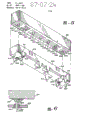
See also Fig. 5 now, on partial, exploded perspective view, can see and adopt dielectric filter of the present invention.Medium sole piece 501 is put into loading bracket 503, and loading bracket has multiple function: provide hard mount pad, so that medium sole piece 501 can be injected in printed circuit board (PCB) or other substrate; By the feed of port 505 and 507, the input and output of having simplified connect and other contact chip by not showing on contact chip 509,510,511,512 and the figure, guarantee the outer conducting surface of medium sole piece 501 and reliable ground between the loading bracket 503. Contact chip 509 and 510 also provides the positioning function of medium sole piece 501 in carriage 503 in addition.Dress carriage 503 also provides microtia sheet 515~525, is used for guaranteeing that carriage and filter are loading on-chip location and fixing, and guarantees carriage 503 and receive to load the reliable ground of substrate to radiofrequency signal.The loading bracket of dielectric filter is at U.S. Patent application No656, and 121, disclosed in " monolithic double-passband filter ", apply on September 27th, 1984 with the Kommrusch name, and transfer assignee of the present invention.But, the carriage that had disclosed before this does not provide the simplification load mode of the carriage among the present invention.
In a preferential concrete device that adopts, dielectric filter 501 is made up of ceramic material, the resonators that utilized 7 holes that interior coating arranged to shorten as equivalence are operated in and are allocated to band pass filter on the radio frequency band that the provincialism automobile telephone uses to constitute one.In this concrete device, ceramic block 501 except resonator coating extends to those zones on the outer surface from the hole, all conformally is covered with conductive coating on all the other all surfaces.Like this, hole 529~535 has its corresponding coating 537~543 in appearance at sole piece 501.These zones 537~543 cut off on electric with ground connection coating, but link ground connection coating by capacitive coupling.In addition, input coating district 547 provides input port 505 and by the capacitive coupling between interior coating hole 529 and the outer filter district 537 formed coaxial resonators thereof, and coating district 549 provides output port 507 and by the capacitive coupling between coating hole 535 and the serving district 543 formed output resonators thereof.Earthing strip 553~558 is plated between the coaxial resonator coating hole, so that adjust the coupling amount between resonator.
When ceramic block 501 inserts carriage 503, allow resonator serving district 537~543 enter carriage 503 down, carriage 503 can play the effect of additional mask like this.Input is installed leg 505 and is connected to coating district 547, and output port 507 is connected to coating 549, as shown in Figure 6.Input port 505 can be a little shunt capacitance, for example resembles the 100B0047 joint that Airpax electronics corporation produces, and its one of protection can be welded little ring 601 and insulating glass pearl 603, to be used for centre of support conductor 605.Little ring 601 usefulness conducting resinls adhere on the carriage 503, to guarantee the reliable installation of input adapter 505.The size of carriage 503 and sole piece 501 makes center conductor 605 just in time can touch coating district face 547.One end of center conductor 605 is linked coating district 547 with the welding or the way of conductive adhesive, connects so that 547 reliable radio frequency to be provided from the center conductor to the cross section.Therefore, the other end of center conductor 605 can be soldered at an easy rate or be inserted into the substrate of fixing this loading bracket 503 and gets on.Output port 507 and corresponding coating district 549 thereof also adopt similar structure.
Fig. 7 has shown the detailed structure of loading bracket 503.The interval that has at length shown the assembling microtia sheet 515~525 in the preferential concrete device that adopts on the figure.These are very important on the operating frequency of filter at interval, are used for guaranteeing the maximum decay of acquisition.All be used for realizing low ground connection inductance in the loading bracket near the assembling slice 517,519 of input and output port (being respectively 505 among Fig. 5 and 507) and at the side of carriage 503 and all the other assembling slices on the bottom.Near the input and output port 501 and carriage 503 between connection guaranteed by contact chip 511 and the 512 such contact chips that are similar near port.All contact chips 509,510,511,512(and on the carriage another side same contact chip, do not draw on the figure) can weld or bond on the medium sole piece 501, can permanently guarantee to electrically contact like this.
Determine that easily the position of assembling microtia sheet 518,520 and 521 is asymmetric.Input/ output end port 505 and 507 also is the center line that departs from carriage 503.This asymmetric performance makes carriage 503 have " selectivity ", makes filter insert printed circuit board (PCB) or other substrate with a direction.
Shown a unique aspect of the present invention among Fig. 8.The dielectric filter sole piece, for example sole piece 501 is put in the carriage 503, becomes a circuit element that is employed, and can insert printed circuit or substrate 801.On printed circuit board (PCB) 801, arrange suitable hole 803 and 805, can make input and output joint 505 and 507 insert (not drawing among Fig. 8) respectively.Meanwhile, on printed circuit board (PCB) 801, arrange suitable location notch hole 815~825, can hold carriage 503 corresponding microtia sheets and insert.Filter 501 just can install on the printed circuit board (PCB) 801 as any other element with carriage 503 like this.Can draw the circuit track from input hole 803 and delivery outlet 805, it is very easy that filter and other circuit are electrically connected.Circuit board track 807 and 809 can be made band line or microstrip line, with the duplexer performance that is improved.
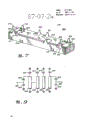
See also Fig. 9, this is the equivalent circuit diagram as the dielectric filter 501 of band pass filter.The input signal that comes from signal source is added to input electrode (547 Fig. 5) through joint 505, it be equivalent to capacitor 924 and 944 among Fig. 9 be 547 and ground connection coating on every side between electric capacity, and capacitor 924 is the electric capacity between electrode 547 and the coaxial resonator that is made of coating hole (529 among Fig. 5).The transmission line 929~935 that the coaxial resonator that is formed by the coating hole 529~535 among Fig. 5 is equivalent to shorten among Fig. 9.Capacitor 937~943 among Fig. 9 has been represented the electric capacity between the ground connection coating of coaxial resonator that the outer extension coating 537~543 by the coating hole among Fig. 5 forms and end face surrounding.Capacitor 925 has been represented the resonator that is made of coating hole 535 among Fig. 5 and the electric capacity between the electrode 594.Capacitor 945 has been represented the electric capacity between electrode 549 and the ground connection coating on every side.Output signal supplies the external circuit utilization from capacitor 925.
See also Figure 10 now, shown on the figure and adopted multiband filter of the present invention, the medium band pass filter 1004 of coupling and 1012 formed in it had by two.Two or more band pass filters of inventing can carry out interior coupling on printed circuit board (PCB) or substrate, to constitute combination or separator, it can be combined into a compound radiofrequency signal to two radiofrequency signals, perhaps a compound radiofrequency signal is divided into two radiofrequency signals by frequency zones.As an application of the concrete device of preferential employing, the device among Figure 10 has utilized the present invention, and it is added to antenna 1008 to transmitting of radio frequency sending set 1002, and the received signal that antenna 1008 is received is delivered to radio-frequency transmitter 1014 simultaneously.Device among Figure 10 can be used as antenna diplexer be used for automobile, portable and the fixed point radio communication very superior.Transmitting of radio frequency sending set 1002 is added to filter 1004 by transmission line 1005, and this transmission line is made of the track on the printed circuit board (PCB) in the concrete device of preferential employing (807 among Fig. 8).Be added to antenna 1008 through filtered transmitting by the printing transmission line on the printed circuit board (PCB) (track 809 among Fig. 8).Filter 1004 is ceramic band-pass filters of the present invention, example the sort of filter as shown in Figure 5 and Figure 8.The centre frequency of filter 1004 passbands just near the emission signal frequency of transmitter 1002, and simultaneously it to received signal frequency very large decay is arranged.In addition, the length of transmission line 1006 is done such selection, thus it to received signal frequency have maximum impedance.
In Figure 10, be added to filter 1012 from the received signal of antenna 1008 by transmission line 1010, this transmission line is made of the printed circuit board (PCB) track.And then be added to radio-frequency transmitter 1014 by printed circuit board (PCB) printing transmission line 1013.Filter 1012 also can be a kind of in the band pass filter of the present invention shown in Fig. 5 and Fig. 8, and its passband central frequency is near the received signal frequency, and it has very large decay to emission signal frequency simultaneously.Similarly, the length of transmission line 1010 is done such selection, so that it transmits with further decay to the impedance that emission signal frequency has maximum.
In the concrete device of the radiofrequency signal duplexer of Figure 10, the frequency range that transmits is 825 to 851 megahertzes (MHZ), and the frequency range of received signal is 825 to 851 megahertzes (MHZ), and these two signals all are added on the antenna of car radio system.Medium band pass filter 1004 and 1012 adopts ceramic dielectric, and make according to the present invention shown in Figure 5.Filter 1004 and 1012, each all is that 3 inches long and 0.45 o'clock are wide.Highly depend primarily on operating frequency, in the preferential concrete device that adopts, the height of emission filter 1004 is 0.49 inch, and the height of receiving filter 1012 is 0.44 inch.The insertion loss of filter 1004 is 2.5dB, and decay to received signal is not less than 50dB.The insertion loss of filter 1012 is 3.0dB, and the decay that transmits is not less than 60dB.The another kind of inner connecting way that the circuit board of medium block filter can be installed is shown in Figure 11.
Sometimes wish that a receiver utilizes two antennas that can carry out switch, the antenna that receives best signal so just can borrow switch control to receive receiver, to finish well-known antenna diversity function.Between transmission line 1006 and 1010 (at the A point), not directly to be coupled with transmission line, but insert a duplexer 1101, be used for selecting one of them for use at common transmit-receive antenna 1103 and single the receipts between antenna 1105 these two antennas, the separated filter 1004 and 1012 that transmits and receives can be coupled in some way with the transmission line 1107 and 1109 with 180 ° of reflection coefficients, so that the function of diversity reception to be provided.
The operating characteristic of filter can be determined by the lip-deep coating shape of medium sole piece, at metal in the spraying plating all not on this surface of this medium block.Dielectric filter, for example as described herein, be to carry out intrinsic coupling by inductance.That is to say that the magnetic field in the medium is being controlled and is being coupled, between resonator, introduce electric capacity, can change inductance value, even offset inductance value.See also Fig. 5 again, can see that realization, these resonators are to borrow coating hole 529~535 and 537~543 formations of overlay coating.As show that ground connection strip electrode 554~557 can limit the capacitive coupling between the resonator.The capacitive coupling that coating crack or additional coating island district form is above-mentioned, and the patent application No656 that is made a report on September 27th, 1984 by Kommrusch disclosed in 121.According to a novel part of the present invention, borrow the incomplete strip shaped electric poles between two resonators on the medium block surface, can obtain controllable capacitive coupling.In the preferential concrete device that adopts, incomplete strip shaped electric poles 553 and 558 between input resonator, output resonator and other resonator has provided in check capacitive coupling, and this just can make inductance coupling high and capacitive coupling between the adjacent resonators combine.In fact, inductance coupling high or capacity coupled employing be respectively in the high-end edge of filter passband, or provide precipitous filter passband edge decay in the low side edge of filter passband.
When the dielectric filter sole piece was combined into diplexer filter, as shown in figure 10, when filter passed through lower frequency, it was favourable adopting the filter that has precipitous decay edge in the passband upper end.Equally, when filter passed through upper frequency, it also was favourable adopting the filter that has precipitous decay edge in the passband lower end.Like this, need not add other filter again and take the device unit that shakes, just can realize receiving and dispatching path supplementary protection each other.
An advantage of dielectric filter sole piece of the present invention is emission filter 1004(Figure 10) in resonator number and spacing can equal resonator number and spacing in the receiving filter 1012.Coupling type is decided by the shape of the coating that adopted.Emission filter 1004 utilizes the inductance coupling high between the resonator, as shown in the coating shape of Figure 12 A.Capacitive coupling between the middle resonator reduces because of adopting complete strip shaped electric poles, and the input and output resonator has bigger electric capacity because of adopting its non-complete strip shaped electric poles that is coupled to intermediate resonator.Receiving filter 1012 utilizes the capacitive coupling between the resonator, as shown in the coating shape of Figure 12 B.Zu Duan coating resonator can not cause capacitive coupling.(adopt coat of metal island district, shown in Figure 12 C, the capacitive coupling amount is increased.)
A novel characteristics of the present invention is to have created the ability that the coupling amount can change with the change of metal level.In addition, the mode of operation of resonator can be from being with the logical band resistance that becomes, as long as one or more resonators are used as transmission zero rather than transmission pole.Figure 12 D has shown the situation that only changes coating realization transmission zero.By coating track 1207 output electrode 1203 is coupled to the first transmission pole resonator 1205.Output electrode 1203 also is coupled to transmission zero resonator 1209 simultaneously.Shown in concrete device in, with transmission zero be tuned to the low side of passband, to realize the additional inhibition of passband lower end.The filter of utilization coat of metal shown in Figure 12 D is applicable to above-mentioned duplexer very much.
Can produce additional zero with the suitable coupling of other resonator.The coat of metal of Figure 12 E is just represented this coupling.
Brief but comprehensive, can be loaded on the dielectric filter that printed circuit board (PCB) has a plurality of resonators, given and disclosed and describe.This filter has utilized coat of metal hole resonator, and its coupled characteristic depends on the coat of metal shape on the face of medium sole piece.The medium sole piece, all plate with electric conducting material on remaining surface except a surface, and the hole resonator extends to medium block from this surface.Layer electrodes around the hole provides the capacitive coupling of this electric conducting material, and the capacitive coupling from a filter to adjacent resonators.Capacitive coupling between the resonator can be controlled by means of an electrode that extends between two adjacent hole resonators to small part, to adjust the capacitive coupling amount between the resonator.The input and output coupling can be finished by the port of symmetrical arrangements on the dress carriage.The little auricle of assembling that is positioned at the groove back side that holds the medium sole piece on the carriage is fastened on the circuit board filter, and makes the filter good earth.Two filters on the printed circuit board (PCB) can constitute a duplexer that is used for machine for receiving and emitting message, and the print copper line on this printed circuit board (PCB) forms the transmission line of suitable electrical length.Therefore, when disclosing and describing a kind of special device of the present invention, should understand that the present invention only is confined to this, can make many corrections because be proficient in the personnel of this skill.。So plan is comprised that all these corrections and any other revise, here because they all belong to and disclosed and proposed within the correct spirit and scope of basic principle of claim.
Claims (6)
1, a kind of filter, it comprises: have the medium apparatus that interior dielectric material is formed, medium apparatus has first surface, and second surface and side surface, the second surface of described medium apparatus and side surface all plate securely with electric conducting material; Have at least on first, second and the 3rd hole face and plate securely with electric conducting material, described conductive coating extends to the second surface of medium apparatus from the first surface of medium apparatus, described first, second is configured on the first surface of this medium apparatus with the 3rd hole, by the predetermined mutually tight commissure of mutual spacing configuration , And; First and second coupling devices are respectively with described first hole and the coupling of the 3rd hole; First, second and the 3rd capacitive means, each described device comprises that the electrode assembly And that is coupled to first, second and the 3rd hole respectively is used for making described first hole and described second hole around described first, second and the 3rd hole respectively, make described second hole and described the 3rd Kong , And make on the side surface of described hole and described medium apparatus conductive coating realize capacitive coupling; Above-mentioned filter is characterized in that:
Have the strip shaped electric poles device to be connected to conductive coating on the side surface of described medium apparatus, described strip shaped electric poles extends partially between two described holes at least to adjust the capacitive coupling between them.
2, according to the filter of claim 1, it is characterized in that: wherein said first and second coupling devices have first and second electrode assemblies be configured in respectively on the end face of medium apparatus near described first hole and the 3rd hole And of place and respectively with described first hole and the coupling of the 3rd hole, wherein said first and second electrode assemblies, each device comprise by described electric conducting material the part end face of topped medium apparatus.
3, according to the filter of claim 1, it is characterized in that: wherein said the 4th capacitive means has the electrode assembly that is inserted between first and second capacitive means, and the capacitive coupling that realizes the described electrode assembly of first and second capacitive means.
4, according to the filter of claim 1, its feature also is to comprise: one the 4th hole, plate securely with electric conducting material on its surface, from the first surface of medium apparatus extend to its second surface And and described the 3rd hole with predetermined arranged spaced on the first surface of this medium apparatus, and tight commissure mutually; And one the 4th capacitive means, be centered around around the 4th hole, in order to the electric conducting material on the side surface of realizing described the 4th hole and described medium apparatus and and described second coupling device between capacitive coupling.
5, a kind of comb filter, adopt one first filter in order to coupling radiofrequency signal And between antenna and first, second radiofrequency signal use device, this first filter and the first radiofrequency signal use device Xiang Ou He And comprise the medium apparatus that dielectric material is formed, it has first surface, all plate securely with electric conducting material second surface and side, the described second surface of medium apparatus and side surface; At least plate securely with electric conducting material on the hole face in first, second and the 3rd hole, described conductive coating extends to the second surface of medium apparatus from the first surface of medium apparatus, described first, second and the 3rd hole are configured in the first surface of medium apparatus, they are by predetermined relative spacing configuration , And and mutually tight commissure; First and second coupling devices, with described first hole and the coupling of the 3rd hole, described first coupling device further is coupled with the first radiofrequency signal use device respectively; First, second and the 3rd capacitive means, each device comprises respectively the electrode assembly with first, second and the coupling of the 3rd hole, these electrode assemblies are respectively around first, second and the 3rd hole, described these capacitive means are used to realize capacitive coupling, i.e. capacitive coupling from described first hole to described second hole, capacitive coupling from described second hole to described the 3rd hole, and the capacitive coupling of the conductive coating on the side from described hole to described medium apparatus; Second filter, it and the second radiofrequency signal use device are coupled, and it comprises that the medium apparatus , And that is made up of dielectric material has first, second and side surface, and the second surface of described medium apparatus and side surface all plate securely with electric conducting material; At least plate securely with electric conducting material on the hole face in first, second and the 3rd hole, described conductive coating extends to the second surface of medium apparatus from the first surface of medium, described first, second and the 3rd hole at least are configured in the first surface of medium apparatus, they are by the predetermined mutually tight commissure of relative spacing configuration , And; First and second coupling devices, with described first hole and the coupling of the 3rd hole, described first coupling device further is coupled with the second radiofrequency signal use device respectively; First, second and the 3rd capacitive means, each device comprises respectively the electrode assembly with first, second and the coupling of the 3rd hole, these electrode assemblies are respectively around first, second and the 3rd hole, described capacitive means is used for realizing capacitive coupling, i.e. capacitive coupling from described first hole to described second hole, capacitive coupling from described two holes to described the 3rd hole, and the capacitive coupling of the conductive coating on from described hole to described medium apparatus side; And second transmission line between second coupling device of second coupling device of described first filter and first transmission line between the antenna and described second filter;
Above-mentioned comb filter is characterized in that comprising:
One strip shaped electric poles device, conductive coating on the side surface of the medium apparatus of at least one filter in the first surface And that it is configured at least one filter in described first and second filters and described first and second filters links to each other, described strip shaped electric poles extends between two described holes at least partly, to adjust the capacitive coupling between them.
6, a kind of She Pin Xin And that is used for by frequency band dielectric filter of stoping the radiofrequency signal of other frequency band to be passed through, comprise that a volume has the dielectric material of first surface, second surface and side surface, described second surface and side surface all plate securely with electric conducting material; With a plurality of by the through hole of described first surface to the above-mentioned dielectric material of perforation of described second surface; All plate with electric conducting material securely at least two surfaces in the above-mentioned hole, and this electric conducting material and above-mentioned second surface are electric common, thereby formed two resonators,
Above-mentioned dielectric filter is characterized in that comprising:
Place the electrode assembly of above-mentioned first surface, this device And that links to each other with the above-mentioned electric conducting material of above-mentioned side surface extends between the first surface hole of hole on the first surface of first resonator in above-mentioned two resonators and second resonator in above-mentioned two resonators partly at least at least, thereby can place restrictions on the coupling between above-mentioned first resonator and above-mentioned second resonator.
Priority Applications (1)
| Application Number | Priority Date | Filing Date | Title |
|---|---|---|---|
| CN 90106515 CN1016028B (en) | 1986-07-25 | 1987-07-24 | Miltiple resonator component-mountable filter |
Applications Claiming Priority (4)
| Application Number | Priority Date | Filing Date | Title |
|---|---|---|---|
| US06/890,686 US4692726A (en) | 1986-07-25 | 1986-07-25 | Multiple resonator dielectric filter |
| US06/890,682 US4716391A (en) | 1986-07-25 | 1986-07-25 | Multiple resonator component-mountable filter |
| US890686 | 1986-07-25 | ||
| US890682 | 1986-07-25 |
Related Child Applications (1)
| Application Number | Title | Priority Date | Filing Date |
|---|---|---|---|
| CN 90106515 Division CN1016028B (en) | 1986-07-25 | 1987-07-24 | Miltiple resonator component-mountable filter |
Publications (2)
| Publication Number | Publication Date |
|---|---|
| CN87105317A CN87105317A (en) | 1988-04-27 |
| CN1011102B true CN1011102B (en) | 1991-01-02 |
Family
ID=27128957
Family Applications (1)
| Application Number | Title | Priority Date | Filing Date |
|---|---|---|---|
| CN87105317A Expired CN1011102B (en) | 1986-07-25 | 1987-07-24 | Multiple resonator component-mountable filter |
Country Status (10)
| Country | Link |
|---|---|
| EP (1) | EP0318478B1 (en) |
| JP (1) | JP2764903B2 (en) |
| CN (1) | CN1011102B (en) |
| AT (1) | ATE118653T1 (en) |
| CA (1) | CA1277729C (en) |
| DE (1) | DE3751062T2 (en) |
| DK (1) | DK64488A (en) |
| FI (1) | FI890243A0 (en) |
| NO (1) | NO173413C (en) |
| WO (1) | WO1988001104A1 (en) |
Cited By (1)
| Publication number | Priority date | Publication date | Assignee | Title |
|---|---|---|---|---|
| CN1053998C (en) * | 1995-05-31 | 2000-06-28 | 株式会社村田制作所 | Dielectric filter and antenna duplexer |
Families Citing this family (13)
| Publication number | Priority date | Publication date | Assignee | Title |
|---|---|---|---|---|
| DK87157C (en) * | 1955-11-16 | 1959-04-13 | Kristian Jacobsen | Hinge. |
| FR2610662B1 (en) * | 1986-12-27 | 1990-07-06 | Scharwaechter Gmbh Co Kg | REMOVABLE DOOR HINGE |
| US5103197A (en) * | 1989-06-09 | 1992-04-07 | Lk-Products Oy | Ceramic band-pass filter |
| JPH0338101A (en) * | 1989-07-04 | 1991-02-19 | Murata Mfg Co Ltd | High frequency coaxial resonator |
| GB2236432B (en) * | 1989-09-30 | 1994-06-29 | Kyocera Corp | Dielectric filter |
| US5045824A (en) * | 1990-09-04 | 1991-09-03 | Motorola, Inc. | Dielectric filter construction |
| GB2263363B (en) * | 1992-01-07 | 1996-05-08 | Marconi Gec Ltd | Electrical filter |
| US5405107A (en) * | 1992-09-10 | 1995-04-11 | Bruno; Joseph W. | Radar transmitting structures |
| JPH0670301U (en) * | 1993-03-15 | 1994-09-30 | 日本電業工作株式会社 | Bandpass filter |
| EP1061662B1 (en) | 1998-11-10 | 2006-01-18 | Matsushita Electric Industrial Co., Ltd. | High-frequency radio circuit |
| JP5906886B2 (en) * | 2012-03-29 | 2016-04-20 | 宇部興産株式会社 | Dielectric resonant component |
| DE102014007927A1 (en) | 2014-05-27 | 2015-12-03 | Kathrein-Werke Kg | High frequency-tight housing, in particular high-frequency-proof filter housing |
| KR102196781B1 (en) | 2018-01-31 | 2020-12-30 | 주식회사 케이엠더블유 | Cavity Filter |
Family Cites Families (8)
| Publication number | Priority date | Publication date | Assignee | Title |
|---|---|---|---|---|
| US4431977A (en) * | 1982-02-16 | 1984-02-14 | Motorola, Inc. | Ceramic bandpass filter |
| JPS59114902A (en) * | 1982-12-21 | 1984-07-03 | Fujitsu Ltd | Dielectric filter |
| JPS60114004A (en) * | 1983-11-25 | 1985-06-20 | Murata Mfg Co Ltd | Dielectric coaxial resonator |
| JPS60152102A (en) * | 1984-01-19 | 1985-08-10 | Murata Mfg Co Ltd | Distributed constant type filter |
| JPS60254802A (en) * | 1984-05-30 | 1985-12-16 | Murata Mfg Co Ltd | Distributed constant type filter |
| JPS6152003A (en) * | 1984-08-21 | 1986-03-14 | Murata Mfg Co Ltd | Dielectric filter |
| GB2165098B (en) * | 1984-09-27 | 1988-05-25 | Motorola Inc | Radio frequency filters |
| JPH0624282B2 (en) * | 1986-07-16 | 1994-03-30 | 株式会社村田製作所 | Filter device |
-
1987
- 1987-05-27 AT AT87903794T patent/ATE118653T1/en not_active IP Right Cessation
- 1987-05-27 EP EP87903794A patent/EP0318478B1/en not_active Expired - Lifetime
- 1987-05-27 DE DE3751062T patent/DE3751062T2/en not_active Expired - Lifetime
- 1987-05-27 JP JP62503469A patent/JP2764903B2/en not_active Expired - Lifetime
- 1987-05-27 WO PCT/US1987/001210 patent/WO1988001104A1/en active IP Right Grant
- 1987-06-05 CA CA000538924A patent/CA1277729C/en not_active Expired - Lifetime
- 1987-07-24 CN CN87105317A patent/CN1011102B/en not_active Expired
-
1988
- 1988-02-09 DK DK064488A patent/DK64488A/en unknown
- 1988-03-23 NO NO881269A patent/NO173413C/en unknown
-
1989
- 1989-01-17 FI FI890243A patent/FI890243A0/en not_active IP Right Cessation
Cited By (1)
| Publication number | Priority date | Publication date | Assignee | Title |
|---|---|---|---|---|
| CN1053998C (en) * | 1995-05-31 | 2000-06-28 | 株式会社村田制作所 | Dielectric filter and antenna duplexer |
Also Published As
| Publication number | Publication date |
|---|---|
| NO173413B (en) | 1993-08-30 |
| DK64488D0 (en) | 1988-02-09 |
| FI890243A (en) | 1989-01-17 |
| NO173413C (en) | 1993-12-08 |
| CN87105317A (en) | 1988-04-27 |
| DE3751062D1 (en) | 1995-03-23 |
| JP2764903B2 (en) | 1998-06-11 |
| FI890243A0 (en) | 1989-01-17 |
| JPH01503428A (en) | 1989-11-16 |
| EP0318478B1 (en) | 1995-02-15 |
| EP0318478A4 (en) | 1989-11-20 |
| DK64488A (en) | 1988-02-11 |
| ATE118653T1 (en) | 1995-03-15 |
| WO1988001104A1 (en) | 1988-02-11 |
| NO881269D0 (en) | 1988-03-23 |
| DE3751062T2 (en) | 1996-01-18 |
| NO881269L (en) | 1988-03-23 |
| CA1277729C (en) | 1990-12-11 |
| EP0318478A1 (en) | 1989-06-07 |
Similar Documents
| Publication | Publication Date | Title |
|---|---|---|
| US4716391A (en) | Multiple resonator component-mountable filter | |
| US4954796A (en) | Multiple resonator dielectric filter | |
| US4829274A (en) | Multiple resonator dielectric filter | |
| EP0831547B1 (en) | Microstrip antenna | |
| US7916086B2 (en) | Antenna component and methods | |
| EP1331687B1 (en) | Composite high frequency apparatus | |
| CN1011102B (en) | Multiple resonator component-mountable filter | |
| EP0746054B1 (en) | Antenna device and communication apparatus incorporating the same | |
| JPH0728165B2 (en) | Ceramic bandpass filter | |
| KR100233744B1 (en) | Antenna switch | |
| US6356244B1 (en) | Antenna device | |
| JPH0983239A (en) | Plane antenna | |
| JP4229418B2 (en) | Circularly polarized patch antenna | |
| CN1016028B (en) | Miltiple resonator component-mountable filter | |
| CN101584079B (en) | Irreversible circuit element and its center conductor assembly | |
| JP3650433B2 (en) | Antenna switch | |
| CA1287667C (en) | Multiple resonator component - mountable filter | |
| CA1290030C (en) | Multiple resonator component - mountable filter | |
| US6392505B1 (en) | Dielectric device | |
| KR950003103B1 (en) | Multiple resonator dielectric filter | |
| JPH10276117A (en) | Composite switch circuit parts | |
| US6850194B2 (en) | Antenna unit | |
| JPH10276003A (en) | Diode switch | |
| KR100320943B1 (en) | chip type splitter | |
| JPH04356801A (en) | Dielectric filter |
Legal Events
| Date | Code | Title | Description |
|---|---|---|---|
| C06 | Publication | ||
| PB01 | Publication | ||
| C10 | Entry into substantive examination | ||
| SE01 | Entry into force of request for substantive examination | ||
| C13 | Decision | ||
| GR02 | Examined patent application | ||
| C14 | Grant of patent or utility model | ||
| GR01 | Patent grant | ||
| C19 | Lapse of patent right due to non-payment of the annual fee | ||
| CF01 | Termination of patent right due to non-payment of annual fee |