CN101088049A - Filter device for the compensation of an asymmetric pupil illumination - Google Patents
Filter device for the compensation of an asymmetric pupil illumination Download PDFInfo
- Publication number
- CN101088049A CN101088049A CNA2005800448498A CN200580044849A CN101088049A CN 101088049 A CN101088049 A CN 101088049A CN A2005800448498 A CNA2005800448498 A CN A2005800448498A CN 200580044849 A CN200580044849 A CN 200580044849A CN 101088049 A CN101088049 A CN 101088049A
- Authority
- CN
- China
- Prior art keywords
- filtering apparatus
- filter element
- illuminator
- pupil
- illumination
- Prior art date
- Legal status (The legal status is an assumption and is not a legal conclusion. Google has not performed a legal analysis and makes no representation as to the accuracy of the status listed.)
- Pending
Links
- 210000001747 pupil Anatomy 0.000 title claims abstract description 154
- 238000005286 illumination Methods 0.000 title claims abstract description 101
- 238000012937 correction Methods 0.000 claims abstract description 15
- 238000001914 filtration Methods 0.000 claims description 81
- 230000003287 optical effect Effects 0.000 claims description 75
- 238000005530 etching Methods 0.000 claims description 6
- 230000005855 radiation Effects 0.000 claims description 5
- 230000015572 biosynthetic process Effects 0.000 claims description 2
- 238000006073 displacement reaction Methods 0.000 claims description 2
- 238000004377 microelectronic Methods 0.000 claims description 2
- 238000003491 array Methods 0.000 claims 1
- 238000000034 method Methods 0.000 claims 1
- 230000001902 propagating effect Effects 0.000 claims 1
- 230000000694 effects Effects 0.000 description 12
- CNQCVBJFEGMYDW-UHFFFAOYSA-N lawrencium atom Chemical compound [Lr] CNQCVBJFEGMYDW-UHFFFAOYSA-N 0.000 description 12
- 230000021615 conjugation Effects 0.000 description 8
- 238000009826 distribution Methods 0.000 description 8
- 238000003780 insertion Methods 0.000 description 7
- 230000037431 insertion Effects 0.000 description 7
- 230000005540 biological transmission Effects 0.000 description 4
- 230000000903 blocking effect Effects 0.000 description 4
- 239000000463 material Substances 0.000 description 4
- 238000005259 measurement Methods 0.000 description 3
- 230000001915 proofreading effect Effects 0.000 description 3
- 230000001154 acute effect Effects 0.000 description 2
- 238000010276 construction Methods 0.000 description 2
- 230000014509 gene expression Effects 0.000 description 2
- 239000011521 glass Substances 0.000 description 2
- 230000010354 integration Effects 0.000 description 2
- 230000033001 locomotion Effects 0.000 description 2
- 230000002085 persistent effect Effects 0.000 description 2
- 239000007787 solid Substances 0.000 description 2
- 241000446313 Lamella Species 0.000 description 1
- VYPSYNLAJGMNEJ-UHFFFAOYSA-N Silicium dioxide Chemical compound O=[Si]=O VYPSYNLAJGMNEJ-UHFFFAOYSA-N 0.000 description 1
- 238000010521 absorption reaction Methods 0.000 description 1
- 238000005422 blasting Methods 0.000 description 1
- WUKWITHWXAAZEY-UHFFFAOYSA-L calcium difluoride Chemical compound [F-].[F-].[Ca+2] WUKWITHWXAAZEY-UHFFFAOYSA-L 0.000 description 1
- 229910001634 calcium fluoride Inorganic materials 0.000 description 1
- 239000002178 crystalline material Substances 0.000 description 1
- 230000002950 deficient Effects 0.000 description 1
- 238000013461 design Methods 0.000 description 1
- 238000010586 diagram Methods 0.000 description 1
- 238000005516 engineering process Methods 0.000 description 1
- 238000003384 imaging method Methods 0.000 description 1
- 238000009434 installation Methods 0.000 description 1
- 238000001393 microlithography Methods 0.000 description 1
- 238000012986 modification Methods 0.000 description 1
- 230000004048 modification Effects 0.000 description 1
- 230000010287 polarization Effects 0.000 description 1
- 230000002035 prolonged effect Effects 0.000 description 1
- 230000001105 regulatory effect Effects 0.000 description 1
- 239000004065 semiconductor Substances 0.000 description 1
- 230000003595 spectral effect Effects 0.000 description 1
- 238000001228 spectrum Methods 0.000 description 1
- 239000013589 supplement Substances 0.000 description 1
- 238000000108 ultra-filtration Methods 0.000 description 1
Images


Classifications
-
- G—PHYSICS
- G02—OPTICS
- G02B—OPTICAL ELEMENTS, SYSTEMS OR APPARATUS
- G02B26/00—Optical devices or arrangements for the control of light using movable or deformable optical elements
- G02B26/007—Optical devices or arrangements for the control of light using movable or deformable optical elements the movable or deformable optical element controlling the colour, i.e. a spectral characteristic, of the light
- G02B26/008—Optical devices or arrangements for the control of light using movable or deformable optical elements the movable or deformable optical element controlling the colour, i.e. a spectral characteristic, of the light in the form of devices for effecting sequential colour changes, e.g. colour wheels
-
- H—ELECTRICITY
- H01—ELECTRIC ELEMENTS
- H01L—SEMICONDUCTOR DEVICES NOT COVERED BY CLASS H10
- H01L21/00—Processes or apparatus adapted for the manufacture or treatment of semiconductor or solid state devices or of parts thereof
- H01L21/02—Manufacture or treatment of semiconductor devices or of parts thereof
- H01L21/027—Making masks on semiconductor bodies for further photolithographic processing not provided for in group H01L21/18 or H01L21/34
- H01L21/0271—Making masks on semiconductor bodies for further photolithographic processing not provided for in group H01L21/18 or H01L21/34 comprising organic layers
- H01L21/0273—Making masks on semiconductor bodies for further photolithographic processing not provided for in group H01L21/18 or H01L21/34 comprising organic layers characterised by the treatment of photoresist layers
- H01L21/0274—Photolithographic processes
-
- G—PHYSICS
- G02—OPTICS
- G02B—OPTICAL ELEMENTS, SYSTEMS OR APPARATUS
- G02B27/00—Optical systems or apparatus not provided for by any of the groups G02B1/00 - G02B26/00, G02B30/00
- G02B27/09—Beam shaping, e.g. changing the cross-sectional area, not otherwise provided for
- G02B27/0933—Systems for active beam shaping by rapid movement of an element
-
- G—PHYSICS
- G01—MEASURING; TESTING
- G01J—MEASUREMENT OF INTENSITY, VELOCITY, SPECTRAL CONTENT, POLARISATION, PHASE OR PULSE CHARACTERISTICS OF INFRARED, VISIBLE OR ULTRAVIOLET LIGHT; COLORIMETRY; RADIATION PYROMETRY
- G01J1/00—Photometry, e.g. photographic exposure meter
- G01J1/02—Details
- G01J1/04—Optical or mechanical part supplementary adjustable parts
- G01J1/0488—Optical or mechanical part supplementary adjustable parts with spectral filtering
-
- G—PHYSICS
- G02—OPTICS
- G02B—OPTICAL ELEMENTS, SYSTEMS OR APPARATUS
- G02B27/00—Optical systems or apparatus not provided for by any of the groups G02B1/00 - G02B26/00, G02B30/00
- G02B27/09—Beam shaping, e.g. changing the cross-sectional area, not otherwise provided for
- G02B27/0938—Using specific optical elements
- G02B27/0994—Fibers, light pipes
-
- G—PHYSICS
- G02—OPTICS
- G02B—OPTICAL ELEMENTS, SYSTEMS OR APPARATUS
- G02B5/00—Optical elements other than lenses
- G02B5/20—Filters
-
- G—PHYSICS
- G03—PHOTOGRAPHY; CINEMATOGRAPHY; ANALOGOUS TECHNIQUES USING WAVES OTHER THAN OPTICAL WAVES; ELECTROGRAPHY; HOLOGRAPHY
- G03F—PHOTOMECHANICAL PRODUCTION OF TEXTURED OR PATTERNED SURFACES, e.g. FOR PRINTING, FOR PROCESSING OF SEMICONDUCTOR DEVICES; MATERIALS THEREFOR; ORIGINALS THEREFOR; APPARATUS SPECIALLY ADAPTED THEREFOR
- G03F7/00—Photomechanical, e.g. photolithographic, production of textured or patterned surfaces, e.g. printing surfaces; Materials therefor, e.g. comprising photoresists; Apparatus specially adapted therefor
- G03F7/70—Microphotolithographic exposure; Apparatus therefor
- G03F7/70058—Mask illumination systems
- G03F7/70091—Illumination settings, i.e. intensity distribution in the pupil plane or angular distribution in the field plane; On-axis or off-axis settings, e.g. annular, dipole or quadrupole settings; Partial coherence control, i.e. sigma or numerical aperture [NA]
-
- G—PHYSICS
- G03—PHOTOGRAPHY; CINEMATOGRAPHY; ANALOGOUS TECHNIQUES USING WAVES OTHER THAN OPTICAL WAVES; ELECTROGRAPHY; HOLOGRAPHY
- G03F—PHOTOMECHANICAL PRODUCTION OF TEXTURED OR PATTERNED SURFACES, e.g. FOR PRINTING, FOR PROCESSING OF SEMICONDUCTOR DEVICES; MATERIALS THEREFOR; ORIGINALS THEREFOR; APPARATUS SPECIALLY ADAPTED THEREFOR
- G03F7/00—Photomechanical, e.g. photolithographic, production of textured or patterned surfaces, e.g. printing surfaces; Materials therefor, e.g. comprising photoresists; Apparatus specially adapted therefor
- G03F7/70—Microphotolithographic exposure; Apparatus therefor
- G03F7/70058—Mask illumination systems
- G03F7/70191—Optical correction elements, filters or phase plates for controlling intensity, wavelength, polarisation, phase or the like
Abstract
The invention relates to a filter device (100) for an illumination system, especially for the correction of the illumination of the illuminating pupil, comprising a light source, with the illumination system being passed through by a boudle of illuminating rays from the light source to an object plane, with the bundle of illuminating rays impinging upon the filter device (100), comprising at least one filter element (105) which can be introduced into the beam path of the bundle of illuminating rays, with the filter element comprising an actuating device (113), so that the filter element can be brought with the help of the actuating device into the bundle of illuminating rays (5).
Description
Technical field
The present invention relates to a kind of compensating illumination system, particularly filtering apparatus of the asymmetric pupil illumination of the illuminator relevant of being used for etching system.
Background technology
Usually the illuminator requirement to the etching system that is used to make microelectronics or micromechanical component is very high.This relates to two kinds of systems as wafer steppers or wafer scanner.This illuminator must be with uniform mode illuminating objects in the plane, field of illuminator, and this object is mask normally.Except this needs, the angle of the illumination in the plane, field distributed also requirement, and itself is relevant with the illumination of the emergent pupil of illuminator.For etching system, the entrance pupil of the emergent pupil of illuminator and the projection objective in downstream coincides.Why Here it is must be provided with the illumination feature of emergent pupil in the mode of adjusting, so that the light of most probable number is incorporated in the projection objective, thereby satisfy the needs of the picture flat focus heart far away (telecentricity) of optical projection system, thereby and make mask structure obtain the uniform imaging of maximum possible.
In order to make the field illumination in the plane even, the illuminator of using shaft-like optical integrator is known.According to the difference of operation wavelength, can adjust the material of this shaft-like optical integrator.Material can comprise quartz glass for example or such as the crystalline material of calcium fluoride.The effect of this shaft-like optical integrator is for example in U.S. Patent No. 5,675, and 401, open among U.S. Patent No. 2004/012766, EP 0867772, U.S. Patent No. 6,236,449 or the EP 0747772.Wherein, owing to be coupled to a plurality of total reflections of the light in the shaft-like optical integrator, realized the mixing fully of illuminating ray on its outer surface.Because bar overlaps surperficial remaining roughness, so total reflection not loss fully.
When using shaft-like optical integrator, since rectangular cross section, undesirable asymmetric in scanner, the appearance of emergent pupil illumination.The light that mainly is parallel to narrow side extension is reflected more continually, and thereby has been weakened more strongly.This asymmetric (energetically) oval-shaped pupil that caused aspect energy distributes, and hereinafter with this asymmetric ellipticity that is called.Asymmetric for fear of what throw light on, from U.S. Patent No. 6,733, known a kind of shaft-like optical integrator in 165, its the aspect ratio between width and the height make on its side surface reflection quantity and and then total reflection loss set by this way, promptly in the space, angle on the output surface that results from glass rod that distributes in advance of luminous energy.This is according to U.S. Patent No. 6,733, and the shortcoming of 165 solution is only oval-shaped asymmetric can the correction.
In addition, adjustable symmetrical pupil light filter is known.For example U.S. Patent No. 6,535, and 274 disclose a kind of light filter arranges, wherein the filter element of at least two symmetries is each other facing to rotating, and then realized a kind of being used for filter adjustable of pupil illumination but the light filter of symmetrical intensity.U.S. Patent No. 6,535, disclosed pupil light filter allows corresponding transmission in the pupil plane zone of the illuminator by setting projection exposure system therefor to produce or proofread and correct the ellipticity of the illumination angle distribution in the object plane in 274.Complicated asymmetric correction is impossible.
U.S. Patent No. 6,636 has illustrated a kind of illuminator in 367, wherein by being arranged at the controlled motion of the pupil light filter in the pupil plane zone, can change light angle.The pupil light filter is configured to have the rotatable element that such transmission distributes, and it is non-rotating symmetry that described transmission distributes around rotation.Thereby, can combine with rod-like element and set ellipticity as integrator.
Known a kind of illuminator from US 2003/0076679, it comprises at least one diffraction grating in the opticpath from light source to the plane that is provided with structure support mask (structure-bearing mask).Diffraction grating is used for respect to optical axis with the different angles reflection ray.
Have be arranged on the optical integrator of light source in the opticpath on the plane that is provided with the structure support mask illuminator further for example from U.S. Patent No. 5,731,577, U.S. Patent No. 5,461,456, U.S. Patent No. 6,333,777 or EP0849637 in disclose.
According to U.S. Patent No. 5,731,577, the optical integrator of U.S. Patent No. 5,461,456, U.S. Patent No. 6,333,777 or EP 0849637 comprises polyhedral element.
Also known a kind of field light filter that is used for improving the field illumination uniformity in the plane, the plane ratio that promptly is configured to leave the theatre is from the near filtering apparatus of the pupil plane of illuminator.EP 1,291 721 discloses a kind of light filter, and wherein the orientation of thin sheet-like element can be set in the surrounding environment on plane on the scene substantially, thereby and can realize local blocking effect in the beam path.But this light filter does not allow the angular spectrum (angularspectrum) of the illumination on correcting field plane, thereby does not allow to proofread and correct relevant with the illumination intensity of the emergent pupil of illuminator asymmetric.
Be that from the shortcoming of all filter elements well known in the prior art they are limited to the specific asymmetric or asymmetric deviation of proofreading and correct pupil, promptly proofread and correct oval asymmetric.Known pupil light filter is unsuitable for proofreading and correct the asymmetric or asymmetric deviation of the complexity in the pupil illumination.
Summary of the invention
In first aspect, the present invention is based on such purpose, a kind of pupil light filter promptly is provided, by this pupil light filter, can overcome the defective of prior art, and especially can by pupil light filter according to the present invention proofread and correct emergent pupil or with all asymmetry of the illumination of the pupil of this emergent pupil conjugation.This relates in particular to a kind of like this illuminator, in this illuminator, has asymmetricly occurred in the illumination of the emergent pupil that not only comprises oval part.
According to the present invention, the filtering apparatus that is associated with emergent pupil comprises a plurality of filter elements, in these filter elements each all radially stretches in the beam path of projection ray bundle basically, described projection ray bundle arrives the plane be provided with such as the structure support mask of optical mask plate (reticle) from light source by illuminator, thereby and produces shadow effect.The degree of blocking effect, promptly covering in the beam path of light can be provided with separately at each filter element.
The preferred crown layout of filter element, this means filter element from the excircle of beam path along introducing towards the direction at the center of beam path.Shadow effect can by set radially insertion depth or the orientation of the filter element by asymmetric formation in the beam path produce.
Further preferably filtering apparatus is to pupil size and and then the σ value of the illumination of emergent pupil do not exerted an influence.This can realize by this way, that is, select the size of filter element in the following manner and arrange density, promptly 1 to 5% of the distance between two filter elements in the maximum shade width of each filter element outer circumferential area that only is beam path.This according to below draw, promptly filter element is provided with stem structure, promptly their lateral dimension usually less than radially the size of (that is, be inserted in the beam path direction).On the other hand, the preferred size of filter element must be selected by this way, and promptly each filter element influences pupil illumination in specific regional area.Regional area should be understood to the pupil surface of a plurality of percentage points.In order to realize the correction to the maximum adjustable joint of the asymmetry of the emergent pupil of illuminator, the preferred filtering apparatus that has more than 20 filter elements that uses.
Determine the possibility of local shadow effect of filter element by setting the insertion depth radially be inserted in the beam path except above-described, as a supplement or interchangeable possibility be, with the asymmetric mode shape of thin slice (for example with) structure filter element, and the incident angle of the filter element in the control bundle path, i.e. orientation.In particularly preferred embodiment, filter element is configured to triangular sheets (paddle).Then, can locate them in two extreme positions.On the one hand, the light beam of beam path will only be mapped on the narrow side of triangular plate.In this case, the blocking effect of filter element generation also is that the shade projection is minimized.On the other hand, plate can also turn in the beam path fully, and such result is maximized for the shade projection.Preferably triangular shaped (it is tapered with acute angle) is used for reducing blocking effect along the direction at the center of beam path continuously by filter element.Orientation by filter element can also combine with the setting of insertion depth radially the setting of cast shadow.
In the structure of external form, can in the subregion, filter element be arranged to partially transparent at least, perhaps filter element can be arranged to unsupported reticulate texture (netstructure).In geometrical construction, there is freedom to construct filter element by this way fully, promptly by setting the orientation of insertion depth and filter element, local shadow effect can be regulated as far as possible individually.Be used to realize that the actuation element in desirable setting and orientation can select by those skilled in the art's judgement.This can realize by for example stepper motor, piezoelectric element or slip-adhesion driver (slip-stick drive).In addition, whole device can be provided with the structure that can rotate around its center, so that compensation is by the position straggling effect that actuation element caused of limited quantity.
In a preferred embodiment, filtering apparatus be arranged in such a way in illuminator emergent pupil or with the surrounding environment of the pupil of this emergent pupil conjugation in, that is, at least a portion of the shade of the filter element in pupil plane projection has the effect of part shade.Therefore, can may mode realize the influence of desired asymmetric feature to pupil illumination with the most accurate, and ring minimum the secondary face of other pupil parameter such as size.The ultimate range of filtering apparatus and pupil plane is selected by this way, and the part shade of filter element arrives the circumferential area of beam path, arrives the center of the part shade of adjacent filter element at the most.This is drawn by the influence that predetermined angle distributes in the pupil illumination according to ultimate range.
The big distance that surpasses this threshold value and select may cause such effect, part shadow region that promptly may be relevant with single filter element may arrive in the part shadow region of (but being a next) filter element, thereby makes the independent adjusting of asymmetric correction become difficult more.In this application, be interpreted as being close to pupil along the range delta z of radiation direction, this scope satisfies such condition, promptly the part shade of each filter element in the circumferential area of light beam at the most crossover half.Being positioned under the situation of range delta z, it is close to the pupil setting when filter element.
The border of range delta z is on the one hand by pupil plane self and on the other hand by ultimate range Δ z
MAXPre-determine.Ultimate range Δ z
MAXFor with the distance of pupil plane, at this pupil plane place, the part shade of corresponding one (but being next) filter element contacts with each other in the circumference range of beam path just.
The part shade of each filter element is produced by the shade projection.In this application, the shade projection should be understood to appear at the shade in the plane that directly is arranged at pupil light filter back.
In a second aspect of the present invention, a kind of filtering apparatus that is used for illuminator is provided, it comprises and can be incorporated at least one filter element in the illuminating bundle path of illuminator with diverse location that described filter element comprises the sensor that is used for determining intensity level.Sensor allows to come the measured intensity value along filter element in the mode of position explanation (position-resolved) in the illuminating bundle path.Filter element can obtain by the intensity level of measured filter element the influence of photocurrent versus light intensity (being the illumination of field in the plane of illuminator).By means of filter element according to the present invention, can measure ellipticity, the focusing heart far away and the transmissivity (these characteristics are as the photocurrent versus light intensity of illumination) of illumination.
The intensity level that records can be read in the control device, and can for example compare with the illumination set-point value to be achieved in field or the pupil plane.These set-point values are corresponding to the set point that is used for filter element, so that realize illumination on the scene and/or the pupil plane.If the filtering apparatus with filter element can and then be avoided the integrated correction of filter element so as the pupil light filter by this further improvement embodiment.This calibration is necessary, reason be the structure of filtering apparatus depend on light illumination mode to a great extent, especially for the position of the filter element of realizing specific illumination on the scene and/or the pupil plane.The type of illumination is called as light illumination mode, for example ring illumination or quadrupole illuminating.In addition, even no longer need filtering apparatus to guarantee after corrective system is installed or when the installation corrective system or during the place-exchange the client, actuated position measured when transporting (ondelievery) is also still effective with respect to the accurate adjusting of illuminator.
Preferably, be used for determining the sensor arrangement success ratio sensor of intensity level, for example photodiode sensor.Sensor can preferably be arranged at the place, an end with the filter element of the formal construction of bar.
Preferably, sensor is connected with control device by this way, that is, signal can exchange by electric wire between sensor and the control device or dedicated radio link.
If sensor is arranged on the place, an end of shaft-like filter element as described above, then absorbed light intensity is determined by the value that records being carried out integration (Integration) because shaft-like filter element is inserted in the illuminating bundle path, the described value that records is determined when the ad-hoc location of outside, field of illumination moves in the field of illumination in quasi-continuous mode when light shape filter element, and the mensuration of intensity depends on the position of sensor.
In further improved second embodiment, shaft-like filter element can be had shape energy sensor covering on schedule, for example photoelectric sensor linear array or CCD linear array fully.This embodiment has such advantage, that is, the measurement of institute's absorption intensity of carrying out according to the position of shaft-like filter element can be carried out when filter element moves in the illuminating bundle path.
Be connected in the shaft-like filter element of end of rod-shaped elements only having a sensor, insert not necessarily continuously.
Because energy sensor only is used for determining the exact position of filter element; so further improving among the embodiment; avoid the persistent radiation that identical light illumination mode produces in order to protect these sensors; filter element can rotate around the axis of himself; so that after measuring by filter element being rotated 180 ° and sensor is arranged in the shade of filter element, thereby and the protection sensor avoid damaging.
If the shaft-like filter element among the particularly above-mentioned further improved embodiment of filter element is provided with sensor, then can along filter element with respect to freely select but fixing coordinate system is measured the light-absorbing share of filter element in the mode of position explanation.Based on this information, can carry out the calculating of set point that is used to set light illumination mode of filter element, so that therefore obtain and/or desired state that pupil illumination is proofreaied and correct.Under the situation of correction on the scene, in the distribution of light in each filter element moves and shows up, so that correct scan-integrated intensity.
By sensor is connected in filter element, also further can determine the edge of pupil, when wherein the edge is in sensor is transferred to the field of illumination and measured.
This makes correcting unit to regulate very accurately with respect to illuminator.
Description of drawings
Fig. 1 shows the synoptic diagram of projection exposure system therefor;
Fig. 2 shows the layout according to the filter element that moves radially of pupil light filter of the present invention;
Fig. 3 shows the pupil light filter with different filter elements that are provided with of Fig. 2;
Fig. 4 shows single filter element;
Fig. 5 shows the structure of the filtering apparatus with a plurality of radial oriented filter elements, and described filter element can rotate around their longitudinal axis;
Fig. 6 shows the three-dimensional plot of rotatable filter element;
Fig. 7 shows the three-dimensional plot of the filter element with transparent region;
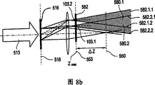
Fig. 8 a shows the related optical component of projection exposure system therefor;
Fig. 8 b shows in detail the shade according to the projection exposure system therefor of Fig. 8 a;
Fig. 8 c shows the cross-sectional view of pupil light filter and is provided with illumination in the plane of filtering apparatus;
Fig. 8 d shows the cross-sectional view of the illumination in the pupil plane;
Fig. 9 a, 9b show correction and the uncorrected illumination of the emergent pupil of the projection exposure system therefor that is used for the dipole illumination shown in Fig. 8 a;
Figure 10 shows the embodiment of the filtering apparatus of shape (similar in other words point-like) sensor on schedule that has that is applied to single rod-shaped elements.
Embodiment
Fig. 1 shows the projection exposure system therefor that is used for micro-lithography, and this projection exposure system therefor is represented with label 1 on the whole.Projection exposure system therefor is used for the structure on the optical mask plate 2 is delivered to the surface of wafer 3.The light source that is used for projection exposure system therefor 1 is a UV laser instrument 4, for example has the ArF excimer laser of 193.3nm wavelength.The illumination beam Shu Shouxian that this laser instrument sends runs into illumination optics device 6.For the reason of clear expression, only show the beam path of the illumination beam bundle 5 between UV laser instrument 4 and illumination optics device 6.Illumination optics device 6 is only schematically shown in Figure 1 with the form of square frame, and it can comprise a plurality of optical modules, such as objective with variable focal length, diffraction optical element or be used to make the optical integrator of illumination beam bundle 5 homogenising.
When by illumination optics device 6, illumination beam bundle 5 is by filtering apparatus, and this filtering apparatus is arranged in the pupil plane 13 or is close to pupil plane 13, and will represent this filtering apparatus with pupil light filter 7 hereinafter.This pupil light filter is constructed according to the present invention, and will do hereinafter in more detail and describe.In the present embodiment, pupil light filter 7 is arranged on pupil plane 13 fronts.The position of pupil light filter 7 also is known as pupil plane hereinafter.Then, illumination beam bundle 5 illuminates optical mask plate 2 (perhaps being called light shield).The structure of optical mask plate 2 projects on the surface of wafer 3 by means of projecting optical device 8.Projecting optical device 8 can be made of a plurality of lens and/or mirror body (mirror).
(it passes the center object point on the optical mask plate 2 to the projected light beam of selecting, and be projected optical devices 8 guiding) in Fig. 1 with reference number 9 expressions, and, for the path that makes projection ray clear, this projected light beam is prolonged a little to enter into reverse direction, promptly towards and enter into the direction of illumination optics device 6.Optical mask plate 2 is positioned at the object plane 10 of projecting optical device 8, and this object plane is represented by dotted lines in Fig. 1.Wafer 3 is positioned at the picture plane 11 of projecting optical device 8, and this also is represented by dotted lines in Fig. 1 as the plane.Also schematically shown the pupil plane 12 of projecting optical device 8 among Fig. 1.In illumination optics device 6, pupil plane 12 and pupil plane 13 conjugation.Also the be known as entrance pupil of projecting optical device 8 of pupil plane 12.
The optical axis of projection exposure system therefor 1 also is represented by dotted lines in Fig. 1, and label is 14.Partially transparent optical sheet 40 is arranged in the illustrated embodiment of projection exposure system therefor along the beam path between UV laser instrument 4 and the illumination optics device 6, the sub-fraction of described plate indirect illumination beam 5, and the overwhelming majority of this light beam of transmission (it typically is) greater than 99%.The beam path that passes the illumination beam bundle 5 of optical sheet 40 only continues to be had on a small quantity, and reason is that it does not need further concern.
By means of projecting optical device 15, the reflecting part of the illumination beam bundle 5 after optical sheet 40 (it is also shown in broken lines) is projected on the ccd array 16 of two dimension.Ccd array is by being connected with control device 18 with the signal wire shown in the dot-and-dash line 17.Control device 18 is by the also accessory drive 20 with the signal wire shown in the dot-and-dash line 19.Drive unit 20 is by also driving the discrete component that is used for asymmetric correction of pupil light filter 7 or pupil light filter with the connection of the driving shown in the dot-and-dash line 21.
Pick-up unit 30 non-active position (inactive position) in the outside, path of projection ray in Fig. 1 illustrates, this sniffer can be used as the alternative of ccd array 16 or uses as replenishing of ccd array 16, with the distribution and the light angle of the illumination intensity that is used for measuring object plane 10 inner projection light beams 9.After optical mask plate 2 removes, pick-up unit 30 can move to by means of the drive unit (not shown) perpendicular to optical axis 14 in the beam path of optical devices by this way, promptly enter the mouth and 32 be positioned at object plane 10, by this inlet, the projected light beam (for example projected light beam 9) that illuminates optical mask plate usually can enter the inside of pick-up unit 30.
Pick-up unit 30 is connected with control device 34 by flexible signal line 33, and this control device 34 self is by being connected with control device 18 with the signal wire shown in the dot-and-dash line 35.
In another optional embodiment of the present invention, pick-up unit 30 is configured to measure the illumination intensity in the picture plane 11 of projecting optical device 8, and wherein wafer also is arranged in this image plane.
Hereinafter, Fig. 2 to Fig. 7 shows the structure of an embodiment of filtering apparatus, and this filtering apparatus can be used as the pupil light filter 7 that is used to carry out asymmetric correction.
Fig. 2 shows first embodiment of the filtering apparatus of pupil light filter 100.It comprises the filter element that can regulate separately.Preferably, filtering apparatus be adjacent to emergent pupil or with the pupil of emergent pupil conjugation.Preferably, single filter element is inserted into the beam path from the outside.In the present embodiment, each filter element 103 is provided with rod shaped structure.Its edge is significantly less than the radially elongation of filter element 103 perpendicular to the size of the azimuth direction of radial direction.
In pupil light filter 100 as shown in Figure 2, radial direction R and azimuth direction φ have been added.
In first embodiment of the invention, filter element 103 is according to required asymmetric correction and along inserting towards the direction of the optical axis HA of the beam path excircle 104 from filtering apparatus 100.But in an illustrated embodiment, the direction of insertion of filter element 103 is consistent with radial direction R.In addition, along azimuth direction φ, the size d of filter element 103 preferably is chosen to less than the distance D between two single adjacent filter elements 103.1,103.2.Distance in excircle 104 zones of filtering apparatus 100 is considered to the distance D between two filter elements 103.1,103.2.Particularly preferably be, horizontal expansion amount d is 1% to 5% of a filter element distance D relative to each other, promptly when the distance of first filter element 103.1 and adjacent second filter element 103.2 was 100mm, the width d of so single filter element 103.1,103.2 was 1mm to 5mm.When selecting this size, the desirable local strength that is used for the asymmetric correction of pupil illumination regulates and can regulate by means of the independent setting of the filter element 103.1,103.2 of filtering apparatus, and it can not impact pupil size itself.
In the embodiment of the invention as shown in Figure 2, pupil illumination is proofreaied and correct in the following manner or is provided with, promptly each single filter element 103 all radially R be inserted in the filtering apparatus with different big degree.For independent insertion depth can radially be set, each filter element 103 is combined with actuation element 113.Actuation element 113 can be used for for each filter element the insertion depth T that R radially enters beam path being set individually.Fig. 4 shows the single shaft-like filter element 103 that is connected with actuation element 113, and actuation element 113 comprises the driver that is used for linear movement (promptly moving along the position of the radial direction R of filter element 100).Be appreciated that the following embodiment of the invention also is fine, promptly wherein only the part of filter element comprise and be used for radially the actuation element that moves that and another part has fixed structure.
In filtering apparatus 100 as shown in Figure 2, depth capacity T
MAXIllustrate with dot-and-dash line 132, by this dot-and-dash line, each filter element 103 can radially move towards the center M of filtering apparatus 100 (especially pupil light filter).
As shown in Figure 2, depth capacity T
MAXSelect in the following manner, promptly depth capacity almost arrives the optical axis HA of beam path, as shown in this embodiment.Preferably, when moving to, each filter element 103 arrives depth capacity T in the filtering apparatus 100
MAXThe time, they are neither overlapped, also are not in contact with one another.By depth capacity T
MAXThe shade that can be provided with at most of predetermined each filter element 103.
Fig. 3 shows and is used for may being provided with of filtering apparatus according to Fig. 2 according to of the present invention.With component identification identical among Fig. 2 identical reference number is arranged.Show in being provided with the plane of filtering apparatus, each filter element 103 extend in the xsect 106 of illumination beam bundle with different big degree.As shown in Figure 1, the illumination beam bundle passes illuminator and arrives the plane that is provided with structure support mask (for example, optical mask plate) from light source.In this case, the illumination beam bundle has circular cross section 106, but is not limited thereto.Circular cross section has circular periphery 107.
The xsect 106 of illumination beam bundle illustrates with level line 109 in Fig. 3.The density of level line 109 is to be used to weigh the standard that light intensity changes in the xsect of beam.Usually be suitable for such situation among the shown figure, promptly light intensity is narrow more, and then light intensity is decayed soon more.
Under the situation of circular illumination φ, radially R obtains parabolic outline.
By shaft-like filter element is incorporated in the illumination, illumination is more effectively cut off along the direction of circular arc, and and then realizes rotational symmetric illumination.It only is in illustrative mode that the circle of the xsect 106 of the beam path among Fig. 3 should be considered to, and be not with the restriction mode shown in because other mode also can be used in the etching system.
Fig. 5 shows the another advantageous embodiment according to filtering apparatus 200 of the present invention.In this case, the shade in the beam path of illumination beam bundle in the filtering apparatus shown in Fig. 2 to 4 obtain by mobile filter element radially.On the contrary, this can obtain by the orientation of control filter element in the beam path of illumination beam bundle.For reaching this purpose, the filter element 203.1,203.2 and 203.3 of filtering apparatus 100 is provided with dissymmetrical structure.Should understand dissymmetrical structure by this way, promptly, when when comparing perpendicular to the second direction 202.2 of first direction 202.1, the part that filter element 203.1,203.2 and 203.3 extend in the beam path has different elongations along the first direction 202.1 perpendicular to radial direction R.This is shown on the filter element 203.3.Filter element 203.3 show first direction 202.1 and second direction 202.2 both.As shown in Figure 5, filter element can be arranged to the shape of thin slice (lamella).If this thin slice is leg-of-mutton and with the tapered words of acute angle, then is particularly preferred.The setting of each filter element 203.1,203.2,203.3 shown in Figure 5 is to carry out around the rotation of rotation RA.1, RA.2, RA.3 by filter element, described rotation be each filter element radially R towards the extension of the mid point M of filtering apparatus 200.Different filter elements 203.1,203.2,203.3 illustrate with different orientation in Fig. 5.Minimum shade projection is shown in first filter element 203.1, and this shows that the projection exposure light beam is mapped to the narrow side of filter element 203.1.Compare with filter element 203.1, second filter element 203.2 has turned over 45 ° around axis RA.2, and consequently, on the plane that is arranged at pupil light filter back, the projection of the shade of filter element 203.2 is increased to the shade projection of ultrafiltration optical element 203.1.With regard to the application's term, the shade projection should be understood to appear at the shade in the plane that directly is arranged at pupil light filter back.The 3rd filter element 203.3 shows in beam path the full rotation with 90 ° angle, and promptly the full-size of filter element has stopped ray, and has obtained the local shade of maximum possible.
Fig. 6 shows the three-dimensional plot of single filter element 203 shown in Figure 5.
Among Fig. 5, filter element 203 shows has the triangular shaped of length L, and this length L is much larger than width B and thickness D.According to the present invention, along the elongation of first direction (it is expressed as directions X in this case) significantly greater than elongation along second direction (it is expressed as the Y direction in this case).
Fig. 6 also shows local rotation RA.Filter element 203 can rotate around this rotation, with the different shade of projection in the plane of pupil back.This figure further shows the center M and the actuation element of pupil light filter, and this actuation element is configured for driving the motor 231 that filter element 203 rotates around rotation RA herein.
The heteroid combination of filter element (described filter element not only can radially be inserted in the beam path but also can with a certain orientation positions in this beam path) is possible, promptly according to the combination of the embodiment of the embodiment of Fig. 2 to 4 and 5 to 6.Such possibility is also arranged, promptly not only filter element is arranged to solid shown in Figure 6, and it fully or in some zone is constructed in the mode of partially transparent.
This filter element has been shown among Fig. 7.Parts identical with filter element shown in Figure 6 are represented with the reference number that has increased by 100.First area 305.2 is configured to solid, and second area 305.1 is constructed with bar 307 in the mode of partially transparent.
Particularly preferably, the partially transparent degree is made by enough thin grating.Preferred especially self-supporting grating is so that avoid as according to the effect of cutting down partially transparent owing to extra border among the embodiment of Fig. 7.
Fig. 8 a shows has the illuminator that is used for the pupil light filter 52 of the asymmetric correction of pupil illumination according to of the present invention.Though compared to Figure 1, in illuminator shown in Figure 8, illustrate in greater detail each optics,, illuminator remains with shown in the mode of highly simplifying.
The lighting device of representing with reference number 510 comprises the light source 512 that is configured to excimer laser generally, described laser instrument produces monochromatic and light height (but incomplete) collimation, and this light has for example wavelength in the ultraviolet spectral limit of 193nm or 157nm.Light source can polarized light-emitting.
The light that is produced by light source 512 is extended to rectangle and substantially parallel beam in optical beam expander 514.Optical beam expander 514 can comprise for example adjustable mirror body layout.Then, the light of now having expanded passes the first optical grating element 516, and this optical grating element can comprise the diffraction optical element with the two-dimensional grating structure described in EP 0747772 A1.First optical element is used for expanding value (entendue value) or so-called photoconduction value are incorporated into system.Laser beam in each position of diffraction optical element with specific angular range (for example, its can between-3 ° and 3 °) diffraction.The angle radiation characteristic of diffraction optical element determined by the design of the diffractive surface structure on the diffraction optical element, is arranged at the variable focal length exhibition and resembles in the pupil plane 550 of object lens (zoom-axicon objective can be adjusted in the object lens of the light intensity distributions in the pupil plane) thereby distribute such as the respective strengths that dipole or four utmost points distribute.The light that originates in light source 512 is changed the distribution of dispersing of conglobate, annular or four utmost points by being used to be provided with the described first optical grating element 516 of dispersing distribution.If under the situation that polarized light source (such as polarization laser) occur, wish illumination, then can use depolariser, so that depolarized to laser.This depolariser for example comprises that first camera is split sheet (camera wedge) and second camera is split sheet, first camera is split sheet and is made by birefringent material, second camera is split the sheet compensation and is split the angle that sheet causes by first camera, and is made by birefringence or non-birefringent material.
The first optical grating element 516 is arranged at variable focal length exhibition and resembles in the object plane 518 of object lens 520, utilizes the variable focal length exhibition to resemble the distribution that object lens can change light angle, thereby and can further form illumination in the pupil.For reaching this purpose, the variable focal length exhibition resembles object lens 520 and comprises two axicon lens 522,524, and these two axicon lens form a pair of and relative to each other movable.
Axicon lens 522,524 can comprise two conical lens.By between these two conical lens, the airspace being set, luminous energy can be transferred to the perimeter.The middle part around optical axis (that is so-called ring section) in the illumination in the pupil plane is formed with hole or the zone with light.
Illuminator shown in Fig. 8 a resembles between object lens and the axicon lens 522,524 in variable focal length exhibition and comprises pupil plane 550, described pupil plane 550 and pupil plane 530 conjugation, and with emergent pupil 560 conjugation of illuminator 510.Pupil light filter 552 according to the present invention is arranged in the pupil plane 550 or is close to this pupil plane, so that proofread and correct asymmetric or asymmetric deviation.The pupil light filter that is used for proofreading and correct asymmetric or asymmetric deviation can also be arranged in another pupil plane that is present in this system or be close to this another pupil plane.Under situation shown in this figure, pupil light filter 552 is Z with the distance of pupil plane 550.Be positioned at regional Δ z apart from Z, Δ z is limited by the pupil plane 550 as boundary on the one hand, on the other hand by distance, delta z
MAXLimit.Distance, delta z
MAXBe such distance, promptly in this distance, the part shade of each filter element in the circumferential area of beam path at most crossovers half.
Fig. 8 b illustrates in greater detail this point.Be denoted by like references with parts identical among Fig. 8 a.Can clearly recognize the illumination beam bundle 513 that begins to send and be mapped to the first optical grating element 516 from the light source (not shown).There is shown object plane 518 and plane 550.In the structure shown in Fig. 8 b, filtering apparatus (that is, according to pupil light filter 552 of the present invention, its mode by example is shown in Figure 3, and represents with reference number 100 in Fig. 3) in plane 553 with distance, delta Z=Z
MAXBe arranged on the pupil plane front.Apart from Z
MAX(wherein filtering apparatus 552 can be arranged to separate with pupil plane 550) provides by this way, promptly the part shade 580.1,580.2 of the single filter element 103.1,103.2 (Fig. 3) of filtering apparatus 552 in pupil plane 550 at most crossovers half.Beam 582.1 and 582.2 marginal ray are represented with reference number 582.1.1,582.1.2,582.2.1,582.2.1.
Fig. 8 c shows filtering apparatus 100 in the plane 553 with vertical view, and this filtering apparatus is identical with filtering apparatus 550 among Fig. 8 a and the 8b.Be provided to identical reference number with parts identical among Fig. 3.Show each filter element 103.1,103.2.Also shown is the xsect of illumination 106.2.Illuminations 106.2 in the plane 553 shown in Fig. 8 c be annular and limit by edge 107.1 and 107.2.
When plane 553 is arranged at distance, delta z=Z with respect to pupil plane 550
MAXThe place, when the illumination of using shown in Fig. 8 c, the mode with xsect in pupil plane 550 has obtained the illumination 106.3 shown in Fig. 8 d.Can clearly see the effect of part shade, this is by causing illumination homogenising (flattening) in the intensity distributions of the illumination 106.3 in the pupil plane with a plurality of filter element 109.1,109.2 corresponding a plurality of minimum value 198.1,198.2 and maximal value 199.1,199.2.Represent with identical reference number with parts identical among Fig. 8 c.Z
MAXBe expressed as such distance, promptly in this distance, the part shade of each filter element of filtering apparatus in pupil plane at most crossovers half.
As in pupil plane 550 or be adjacent to substituting that pupil plane 550 is provided with, also can be arranged in the pupil plane 530 or be close to the setting of second pupil plane 530 according to filtering apparatus 552 of the present invention, for example, be arranged between second object lens 528 and second pupil plane 530.
In Fig. 8 a, optical grating element 532 is last optical element that change expansion (entendue) or so-called photoconduction value in the lighting device 510.Thereby the expansion that is realized to greatest extent by lighting device 510 arrives the back of optical grating element 532.Expanding value only approximately be between the first optical grating element 516 and the second optical grating element 532 expanding value (its can the second optical grating element, 532 back obtain) 1% to 10%.This means that the light that passes second object lens 528 relatively is still very collimation.Therefore, second object lens 528 can be with very simple and inexpensive manner structure.
Along the direction of the light ray propagation of the second optical grating element, 532 back, the 3rd object lens 534 are provided with by this way, promptly are provided with the known mask device 538 with scalable bladed edge (knife edge) in Qi Chang plane 536.Mask device 538 is determined the shape in the zone that penetrated by projection ray on optical mask plate 540.The 4th object lens 542 be used for by the edge limited region projection of bladed in mask plane 540.
Selectively, the glass bar (not shown) that is used for beam uniformity can be inserted between the 3rd object lens 534 and the mask device 538.
The emergent pupil of representing whole illuminator 510 among Fig. 8 with label 560.The pupil plane the 530, the 550th of illuminator is with the plane of emergent pupil 560 conjugation.The emergent pupil 560 of illuminator coincides with the entrance pupil of projection objective 570, and described projection objective 570 projects to optical mask plate on the photosensitive object 564 in the object plane 562.
Object lens described in the disclosed application DE 10151309 are as projection objective.Therefore, the open scope of this application all comprises in this application.
Fig. 9 a to 9b shows the example that is used for the dipole-like pupil illumination, and it occurs in in the illuminator shown in Fig. 8 a and the emergent pupils 560 pupil plane 550 conjugation.Fig. 9 a shows the asymmetric pupil illumination in the emergent pupil 560, and it is not also proofreaied and correct by filter element according to the present invention.Fig. 9 b shows the position that is inserted into the filter element in the beam path, and described filter element is according to a certain distance that is arranged on the pupil plane front of the present invention, thereby only generating unit is divided shade.In addition, reduce the part that shows consequent intensity, this part make pupil illumination symmetry in the emergent pupil 560.Must be noted that this relates to very the example of simplifying, because the preferred filtering apparatus of institute comprises 10 among the present invention, preferably 20 and the more independent controllable filter element as shown in Fig. 2 to 7.
Particularly preferred, not to be arranged in the pupil plane with filtering apparatus, but be arranged at the outside of pupil plane, promptly be close to pupil plane with distance, delta z.The part shadow effect appears in this case.The result who only is close to the pupil plane setting is that only the shape to pupil produces very little influence.On the other hand, realized necessary gamma correction, so that proofread and correct the asymmetry of pupil.Therefore, the setting of the filtering apparatus of close pupil plane is preferred according to the present invention.Can also be not all filter elements of filtering apparatus be arranged in the plane.This means that each filter element can relative to each other have distance along the direction of beam propagation.The result of this measure is that selected filter element can be associated with predetermined part shadow region.The another improvement according to the present invention, filter element can be along the independent displacement of the direction of light beam, so that have the various possibilities that are used for adjustment member shade (it is different for each filter element).
Figure 10 shows the embodiment that is arranged at the sensor on the shaft-like filter element 1003.1,1003.2,1003.3,1003.4,1003.5,1003.6,1003.7,1003.8 that has of the present invention.
In shaft-like filter element 1003.1,1003.2,1003.3,1003.4,1003.5,1003.6,1003.7,1003.8, sensor is arranged at 1004.1,1004.2,1004.3,1004.4,1004.5,1004.6,1004.7,1004.8 places, end respectively.In shaft-like filter element 1003.3, whole shaft-like filter element is provided with sensor 1005.3.1,1005.3.2,1005.3.3,1005.3.4,1005.3.5,1005.3.6,1005.3.7,1005.3.8.
Sensor 1005.1,1005.2,1005.3.1,1005.3.2,1005.3.3,1005.3.4,1005.3.5,1005.3.6,1005.3.7,1005.3.8,1005.4,1005.5,1005.6,1005.7,1005.8 allow in the illuminating bundle path along the mode measured intensity value of filter element with position resolution.The intensity level of the filter element that records allows with regard to filter element the influence of the photocurrent versus light intensity of ellipticity, the focusing heart far away and transmissivity to be drawn a conclusion.
Figure 10 further shows control device 1010, and this control device is configured to personal computer, and 1012.1,1012.2 is connected with sensor 1005.1,1005.8 by going between in the illustrated case.
The intensity level that records by sensor 1005.1,1005.8 can be read in the control device 1010, and can compare with the illumination set-point value to be achieved in field or the pupil plane.Then, these set-point values are corresponding to the set point that is used for filter element, so that realize illumination on the scene and/or the pupil plane.Then, as the result of this measurement, shaft-like filter element can take corresponding set point to by actuation element (not shown among Figure 10).
Preferably, sensor 1005.1,1005.2,1005.3.1,1005.3.2,1005.3.3,1005.3.4,1005.3.5,1005.3.6,1005.3.7,1005.3.8,1005.4,1005.5,1005.6,1005.7,1005.8 are configured to the power sensor, photodiode sensor for example is so that measure intensity level.
In the second shaft-like filter element 1005.3, shaft-like filter element is coated with shape power sensor on schedule fully.Sensor 1005.3.1,1005.3.2,1005.3.3,1005.3.4,1005.3.5,1005.3.6,1005.3.7,1005.3.8 are configured to the line or the CCD line of photodiode sensor.The advantage that this structure has is, can take place in the filter element in being displaced to the illuminating bundle path the measurement of the intensity that absorbed, and the intensity that this absorbed depends on the position of shaft-like filter element.
Because power sensor only is used for determining the exact position of filter element; so avoid persistent radiation because of identical light illumination mode in order to protect these sensors; in another improvement embodiment, provide; filter element can rotate around the axis of himself; so that after measuring by filter element being rotated 180 ° and sensor is arranged in the shade of filter element, thereby and the protection sensor avoid damaging.
As mentioned above, can be used as the filter element of pupil plane illumination according to filtering apparatus (wherein shaft-like filter element is equipped with power sensor) shown in Figure 10.Filter element can also be set by this way, promptly pass through according to the illumination in the pupil filter element correcting field of the present invention plane.
When photodiode sensor is used as sensor, all blasting for fear of the dynamic range of diode, below can be provided in the preferred embodiments of the present invention, that is, variable attenuator is set in light source (for example LASER Light Source) back and in the illumination optics device front.
Though invention has been described with reference to embodiment, the present invention should not be limited to these embodiment, and the application also comprise those by claim to disclosed modification of those skilled in the art and variation.
Claims (28)
1. filtering apparatus that is used for illuminator, is subjected to the illumination of irradiation pupil especially for correction, wherein said illuminator comprises light source (4) and propagates into the illumination beam bundle (5) of object plane (10) from described light source (4) that wherein the described illumination beam bundle of propagating by described illuminator along beam path (5) is mapped on the described filtering apparatus (7);
Described filtering apparatus comprises:
At least one filter element (103), it be directed in the described beam path of described illumination beam bundle (5), wherein,
Described filter element (103) comprises actuation element (113), thereby described filter element (103) can be brought to the diverse location in the described illumination beam bundle (5) by means of described actuation element (113).
2. filtering apparatus according to claim 1 is characterized in that, at least one filter element (103) comprises at least one sensor that is used for determining light intensity.
3. filtering apparatus according to claim 1 and 2 is characterized in that, described filtering apparatus (7) comprises a plurality of filter elements (103).
4. filtering apparatus according to claim 3 is characterized in that, at least a portion of described a plurality of filter elements (103) is combined with actuation element (113).
5. according to each described filtering apparatus in the claim 2 to 4, it is characterized in that described filtering apparatus (7) comprises excircle (104), and described a plurality of filter element (103) is provided with radially basically on described excircle (104).
6. according to each described filtering apparatus in the claim 1 to 5, it is characterized in that described filter element (103) is arranged to shaft-like.
7. filtering apparatus according to claim 6 is characterized in that, is used for determining that described at least one sensor of described light intensity is arranged at an end of described filter element.
8. filtering apparatus according to claim 7 is characterized in that, is used for determining that a plurality of sensors of lighting radiation intensity are along described shaft-like filter element setting.
9. according to each described filtering apparatus in the claim 2 to 8, it is characterized in that the described sensor of determining described light intensity is a power sensor.
10. filtering apparatus according to claim 8 is characterized in that, along the described a plurality of sensors formation photodiode sensor linear arrays or the CCD linear array of described shaft-like filter element.
11., it is characterized in that the length of described filter element (103) is different with width according at least one described filtering apparatus in the claim 1 to 10.
12. according at least one described filtering apparatus in the claim 1 to 11, it is characterized in that, described filtering apparatus (7) has circular outer perimeter (104), and the structure that described filter element has makes and can move towards the center of the circle of described excircle along described radial direction.
13., it is characterized in that described filter element has transparent structure at least in the subregion according at least one described filtering apparatus in the claim 1 to 12.
14., it is characterized in that described filter element has unsupported reticulate texture at least in the subregion according at least one described filtering apparatus in the claim 1 to 13.
15. according at least one described filtering apparatus in the claim 1 to 14, it is characterized in that described filtering apparatus is arranged in such a way, promptly described filter element along described radially be movably.
16. according at least one described filtering apparatus in the claim 1 to 15, it is characterized in that, described filtering apparatus is arranged in such a way, and promptly described filter element can rotate around radial oriented axis basically, and/or can be along axis displacement in the axial direction.
17. according at least one described filtering apparatus in the claim 1 to 16, it is characterized in that, use more than 10 filter elements, particularly more than 20 filter elements.
18. illuminator, it comprises filtering apparatus, described filtering apparatus comprises a plurality of filter elements, actuation element combines with at least a portion of described filter element, so that the filter element that will be combined with described actuation element moves to diverse location in the beam path of the illumination beam bundle by described illuminator, and described filtering apparatus is arranged in the pupil plane of described illuminator or near described pupil plane and be provided with.
19. illuminator according to claim 18, it is characterized in that, described filtering apparatus is arranged in the distance range Δ z with respect to the pupil plane of described illuminator, and first border of described distance range is given by described pupil plane, and second border of described distance range is by Δ z
MAXGiven, distance, delta z
MAXLimit by this way,
The part shade that is described filter element contacts with each other in the described circumferential area of described beam path just.
20. according to each described illuminator in the claim 1 to 19, it is characterized in that, described illuminator comprises optical grating element (516) in the described opticpath from described light source (4) to object plane (10), it is characterized in that described filtering apparatus (7) is arranged on the back of described optical grating element (516) along described opticpath.
21. illuminator according to claim 20 is characterized in that, described illuminator comprises that also objective with variable focal length or variable focal length exhibition resemble object lens (6), and described filtering apparatus (7) is arranged in the described object lens (6).
22. according to claim 20 or 21 described illuminators, it is characterized in that, described optical grating element (516) is the first optical grating element, and described illuminator comprises the second optical grating element (532) that is positioned at described first optical grating element (516) downstream along described opticpath.
23. illuminator according to claim 22 is characterized in that, described filtering apparatus (7) is arranged at the front of described second optical element (532) with optical grating element along described opticpath.
24., it is characterized in that described filtering apparatus is according to each described filtering apparatus in the claim 2 to 17 according to each described illuminator in the claim 18 to 23.
25., it is characterized in that described illuminator comprises variable attenuator according to each described illuminator in the claim 18 to 24 the described opticpath from light source (4) to object plane (10).
26. illuminator according to claim 25 is characterized in that, described variable attenuator is arranged at the front of described illumination optics device along described opticpath.
27. an etching system, it has according to each described illuminator in the claim 18 to 26.
28. a method that is used to make microelectronics or micromechanical component is characterized in that, uses etching system according to claim 27.
Applications Claiming Priority (2)
| Application Number | Priority Date | Filing Date | Title |
|---|---|---|---|
| DE102004063314.2 | 2004-12-23 | ||
| DE102004063314A DE102004063314A1 (en) | 2004-12-23 | 2004-12-23 | Filter device for compensating an asymmetrical pupil illumination |
Publications (1)
| Publication Number | Publication Date |
|---|---|
| CN101088049A true CN101088049A (en) | 2007-12-12 |
Family
ID=35033385
Family Applications (1)
| Application Number | Title | Priority Date | Filing Date |
|---|---|---|---|
| CNA2005800448498A Pending CN101088049A (en) | 2004-12-23 | 2005-08-25 | Filter device for the compensation of an asymmetric pupil illumination |
Country Status (8)
| Country | Link |
|---|---|
| US (5) | US7798676B2 (en) |
| EP (2) | EP2278403A1 (en) |
| JP (1) | JP4700697B2 (en) |
| KR (2) | KR101182940B1 (en) |
| CN (1) | CN101088049A (en) |
| DE (1) | DE102004063314A1 (en) |
| TW (1) | TW200622313A (en) |
| WO (1) | WO2006066638A1 (en) |
Cited By (4)
| Publication number | Priority date | Publication date | Assignee | Title |
|---|---|---|---|---|
| CN103512594A (en) * | 2012-06-20 | 2014-01-15 | 通用电气公司 | Overhead occupancy sensor |
| CN104216234A (en) * | 2013-06-05 | 2014-12-17 | 中芯国际集成电路制造(上海)有限公司 | Method for detecting light source symmetry of lithography system |
| CN105739250A (en) * | 2016-05-13 | 2016-07-06 | 上海华力微电子有限公司 | Compensation device for uniformity of lighting pupil of photoetching machine and compensation method of compensation device |
| CN108983559A (en) * | 2018-08-08 | 2018-12-11 | 中国科学院上海光学精密机械研究所 | Litho machine pupil corrector and its application method |
Families Citing this family (22)
| Publication number | Priority date | Publication date | Assignee | Title |
|---|---|---|---|---|
| JP4599936B2 (en) | 2004-08-17 | 2010-12-15 | 株式会社ニコン | Illumination optical apparatus, adjustment method of illumination optical apparatus, exposure apparatus, and exposure method |
| DE102006059024A1 (en) * | 2006-12-14 | 2008-06-19 | Carl Zeiss Smt Ag | Projection exposure equipment for microlithography, has illuminating optical unit for illuminating object field in object plane and correction screen is arranged in or adjacent to aperture diaphragm plane of projection optical unit |
| US7990520B2 (en) | 2006-12-18 | 2011-08-02 | Carl Zeiss Smt Gmbh | Microlithography illumination systems, components and methods |
| WO2008092653A2 (en) | 2007-01-30 | 2008-08-07 | Carl Zeiss Smt Ag | Illumination system of a microlithographic projection exposure apparatus |
| US7843549B2 (en) * | 2007-05-23 | 2010-11-30 | Asml Holding N.V. | Light attenuating filter for correcting field dependent ellipticity and uniformity |
| US8908151B2 (en) * | 2008-02-14 | 2014-12-09 | Nikon Corporation | Illumination optical system, exposure apparatus, device manufacturing method, compensation filter, and exposure optical system |
| DE102008001511A1 (en) * | 2008-04-30 | 2009-11-05 | Carl Zeiss Smt Ag | Illumination optics for EUV microlithography and illumination system and projection exposure apparatus with such illumination optics |
| NL1036905A1 (en) * | 2008-06-03 | 2009-12-04 | Asml Netherlands Bv | Lithographic apparatus and device manufacturing method. |
| CN102203675B (en) | 2008-10-31 | 2014-02-26 | 卡尔蔡司Smt有限责任公司 | Illuminating optic for EUV microlithography |
| JP5541164B2 (en) | 2008-12-24 | 2014-07-09 | 株式会社ニコン | Illumination optical system, exposure apparatus, and device manufacturing method |
| DE102010042901B3 (en) * | 2010-10-26 | 2012-04-05 | Carl Zeiss Smt Gmbh | Polarisationsaktuator |
| DE102011077234A1 (en) | 2011-06-08 | 2012-12-13 | Carl Zeiss Smt Gmbh | Extreme UV mirror arrangement for use as e.g. pupil facet mirror arranged in region of pupil plane of e.g. illumination system, has multilayer arrangement including active layer arranged between entrance surface and substrate |
| JP6093753B2 (en) | 2011-03-23 | 2017-03-08 | カール・ツァイス・エスエムティー・ゲーエムベーハー | EUV mirror mechanism, optical system with EUV mirror mechanism, and method of operating an optical system with EUV mirror mechanism |
| DE102011005940A1 (en) | 2011-03-23 | 2012-09-27 | Carl Zeiss Smt Gmbh | Extreme ultraviolet mirror arrangement for optical system for extreme ultraviolet microlithography, comprises multiple mirror elements that are arranged side by side, such that mirror elements form mirror surface |
| CN102331688B (en) * | 2011-10-25 | 2013-06-26 | 中国科学院光电技术研究所 | Pupil uniformity compensation device |
| US9261793B2 (en) | 2012-09-14 | 2016-02-16 | Globalfoundries Inc. | Image optimization using pupil filters in projecting printing systems with fixed or restricted illumination angular distribution |
| DE102013213545A1 (en) * | 2013-07-10 | 2015-01-15 | Carl Zeiss Smt Gmbh | Illumination optics for projection lithography |
| US9721421B2 (en) | 2015-05-05 | 2017-08-01 | Mladen Blazevic | Electronic gaming system with physical gaming chips and wager display |
| DE102015220144A1 (en) * | 2015-10-16 | 2017-04-20 | Carl Zeiss Smt Gmbh | Optical system and lithography system |
| CN106556974B (en) * | 2015-09-30 | 2019-04-26 | 中芯国际集成电路制造(上海)有限公司 | Lithography illuminating system and lithographic equipment |
| WO2017144265A1 (en) | 2016-02-25 | 2017-08-31 | Asml Netherlands B.V. | Beam homogenizer, illumination system and metrology system |
| DE102021120952B3 (en) | 2021-08-11 | 2022-11-10 | Carl Zeiss Smt Gmbh | Method for correcting a telecentricity error of an imaging device and mask inspection microscope |
Family Cites Families (33)
| Publication number | Priority date | Publication date | Assignee | Title |
|---|---|---|---|---|
| JPS5928337A (en) * | 1982-08-09 | 1984-02-15 | Hitachi Ltd | Projection aligner |
| US5131577A (en) * | 1988-05-17 | 1992-07-21 | Ford Motor Company | Apparatus for making a powder metal connecting rod |
| JPH0812754B2 (en) * | 1990-08-20 | 1996-02-07 | 富士通株式会社 | Boost circuit |
| US6769792B1 (en) * | 1991-04-30 | 2004-08-03 | Genlyte Thomas Group Llc | High intensity lighting projectors |
| US5282121A (en) * | 1991-04-30 | 1994-01-25 | Vari-Lite, Inc. | High intensity lighting projectors |
| JP3158691B2 (en) * | 1992-08-07 | 2001-04-23 | 株式会社ニコン | Exposure apparatus and method, and illumination optical apparatus |
| US5461456A (en) * | 1992-11-24 | 1995-10-24 | General Signal Corporation | Spatial uniformity varier for microlithographic illuminator |
| KR960006377B1 (en) * | 1993-11-17 | 1996-05-15 | 삼성전자주식회사 | Word-line loading compensation circuit of semiconductor memory device |
| DE19520563A1 (en) | 1995-06-06 | 1996-12-12 | Zeiss Carl Fa | Illumination device for a projection microlithography device |
| EP0687956B2 (en) * | 1994-06-17 | 2005-11-23 | Carl Zeiss SMT AG | Illumination device |
| US5774222A (en) * | 1994-10-07 | 1998-06-30 | Hitachi, Ltd. | Manufacturing method of semiconductor substrative and method and apparatus for inspecting defects of patterns on an object to be inspected |
| JPH08293461A (en) | 1995-04-21 | 1996-11-05 | Nikon Corp | Lighting system and projection aligner using it |
| DE69619972D1 (en) * | 1996-06-18 | 2002-04-25 | St Microelectronics Srl | Non-volatile memory device with low supply voltage and voltage booster |
| JPH10153866A (en) | 1996-11-22 | 1998-06-09 | Nikon Corp | Illuminator and exposure device provided with it |
| JP3005203B2 (en) | 1997-03-24 | 2000-01-31 | キヤノン株式会社 | Illumination apparatus, exposure apparatus, and device manufacturing method |
| US6333777B1 (en) | 1997-07-18 | 2001-12-25 | Canon Kabushiki Kaisha | Exposure apparatus and device manufacturing method |
| JPH11271619A (en) * | 1998-03-19 | 1999-10-08 | Nikon Corp | Illumination optical device and exposure device provided with illumination optical device |
| TWI226972B (en) * | 2000-06-01 | 2005-01-21 | Asml Netherlands Bv | Lithographic apparatus, device manufacturing method, and device manufactured thereby |
| DE10043315C1 (en) | 2000-09-02 | 2002-06-20 | Zeiss Carl | Projection exposure system |
| DE10046218B4 (en) | 2000-09-19 | 2007-02-22 | Carl Zeiss Smt Ag | Projection exposure system |
| DE10065198A1 (en) * | 2000-12-20 | 2002-07-11 | Zeiss Carl | Light integrator for a lighting device |
| US6886964B2 (en) * | 2001-06-26 | 2005-05-03 | Allan Gardiner | Illuminator with filter array and bandwidth controller |
| EP1291721B1 (en) | 2001-09-07 | 2008-02-27 | ASML Netherlands B.V. | Lithographic apparatus and device manufacturing method |
| US6741329B2 (en) * | 2001-09-07 | 2004-05-25 | Asml Netherlands B.V. | Lithographic apparatus and device manufacturing method |
| DE10151309A1 (en) | 2001-10-17 | 2003-05-08 | Carl Zeiss Semiconductor Mfg S | Projection exposure system for microlithography for lambda <200 nm |
| US6775069B2 (en) | 2001-10-18 | 2004-08-10 | Asml Holding N.V. | Advanced illumination system for use in microlithography |
| DE10158921A1 (en) | 2001-11-30 | 2003-06-26 | Zeiss Carl Smt Ag | Method for determining at least one parameter which is characteristic of the illumination angle distribution of a light source of a projection exposure system serving to illuminate an object |
| EP1870772B1 (en) | 2002-03-18 | 2013-10-23 | ASML Netherlands B.V. | Lithographic apparatus |
| DE60326063D1 (en) * | 2002-03-18 | 2009-03-19 | Asml Netherlands Bv | Lithographic apparatus and method for making an article |
| EP1372040B1 (en) | 2002-06-11 | 2008-03-05 | ASML Netherlands B.V. | Lithographic apparatus and device manufacturing method |
| US7023524B2 (en) * | 2003-12-18 | 2006-04-04 | Asml Netherlands B.V. | Lithographic apparatus and device manufacturing method |
| US7283209B2 (en) * | 2004-07-09 | 2007-10-16 | Carl Zeiss Smt Ag | Illumination system for microlithography |
| US7403418B2 (en) * | 2005-09-30 | 2008-07-22 | Silicon Storage Technology, Inc. | Word line voltage boosting circuit and a memory array incorporating same |
-
2004
- 2004-12-23 DE DE102004063314A patent/DE102004063314A1/en not_active Withdrawn
-
2005
- 2005-08-25 KR KR1020117015632A patent/KR101182940B1/en not_active IP Right Cessation
- 2005-08-25 WO PCT/EP2005/009165 patent/WO2006066638A1/en active Application Filing
- 2005-08-25 US US11/722,631 patent/US7798676B2/en active Active
- 2005-08-25 KR KR1020077013078A patent/KR101156369B1/en active IP Right Grant
- 2005-08-25 JP JP2007547201A patent/JP4700697B2/en not_active Expired - Fee Related
- 2005-08-25 EP EP10007886A patent/EP2278403A1/en not_active Withdrawn
- 2005-08-25 EP EP05782800A patent/EP1828844A1/en not_active Withdrawn
- 2005-08-25 CN CNA2005800448498A patent/CN101088049A/en active Pending
- 2005-08-29 TW TW094129565A patent/TW200622313A/en not_active IP Right Cessation
-
2010
- 2010-08-12 US US12/855,305 patent/US8025427B2/en not_active Expired - Fee Related
-
2011
- 2011-08-23 US US13/215,910 patent/US8246211B2/en not_active Expired - Fee Related
-
2012
- 2012-07-19 US US13/553,005 patent/US8480261B2/en not_active Expired - Fee Related
-
2013
- 2013-06-13 US US13/917,505 patent/US8636386B2/en not_active Expired - Fee Related
Cited By (5)
| Publication number | Priority date | Publication date | Assignee | Title |
|---|---|---|---|---|
| CN103512594A (en) * | 2012-06-20 | 2014-01-15 | 通用电气公司 | Overhead occupancy sensor |
| CN103512594B (en) * | 2012-06-20 | 2017-09-01 | 通用电气公司 | overhead occupancy sensor |
| CN104216234A (en) * | 2013-06-05 | 2014-12-17 | 中芯国际集成电路制造(上海)有限公司 | Method for detecting light source symmetry of lithography system |
| CN105739250A (en) * | 2016-05-13 | 2016-07-06 | 上海华力微电子有限公司 | Compensation device for uniformity of lighting pupil of photoetching machine and compensation method of compensation device |
| CN108983559A (en) * | 2018-08-08 | 2018-12-11 | 中国科学院上海光学精密机械研究所 | Litho machine pupil corrector and its application method |
Also Published As
| Publication number | Publication date |
|---|---|
| WO2006066638A1 (en) | 2006-06-29 |
| KR101156369B1 (en) | 2012-06-13 |
| US8636386B2 (en) | 2014-01-28 |
| US20110299285A1 (en) | 2011-12-08 |
| DE102004063314A1 (en) | 2006-07-13 |
| JP4700697B2 (en) | 2011-06-15 |
| US8480261B2 (en) | 2013-07-09 |
| US8025427B2 (en) | 2011-09-27 |
| EP2278403A1 (en) | 2011-01-26 |
| KR20070085995A (en) | 2007-08-27 |
| US20080113281A1 (en) | 2008-05-15 |
| US8246211B2 (en) | 2012-08-21 |
| US20130278913A1 (en) | 2013-10-24 |
| WO2006066638A8 (en) | 2006-08-24 |
| TWI303325B (en) | 2008-11-21 |
| US20120281198A1 (en) | 2012-11-08 |
| TW200622313A (en) | 2006-07-01 |
| EP1828844A1 (en) | 2007-09-05 |
| JP2008525828A (en) | 2008-07-17 |
| US7798676B2 (en) | 2010-09-21 |
| KR20110094121A (en) | 2011-08-19 |
| KR101182940B1 (en) | 2012-09-13 |
| US20100309450A1 (en) | 2010-12-09 |
Similar Documents
| Publication | Publication Date | Title |
|---|---|---|
| CN101088049A (en) | Filter device for the compensation of an asymmetric pupil illumination | |
| JP3993335B2 (en) | Lithographic apparatus and method | |
| US4988188A (en) | Illumination device | |
| KR101220667B1 (en) | Illuminating optical apparatus, exposure apparatus, exposure method, and device manufacturing method | |
| KR101470769B1 (en) | Illumination system of a microlithographic projection exposure apparatus | |
| JPH1154426A (en) | Lighting device and aligner using the same | |
| CN102804072A (en) | Faceted mirror for use in microlithography | |
| KR20100087325A (en) | Illumination optical system, exposure apparatus, and device manufacturing method | |
| KR20000048227A (en) | Method and apparatus for illuminating a surface using a projection imaging apparatus | |
| US7027129B2 (en) | System for laser beam expansion without expanding spatial coherence | |
| KR20090045911A (en) | Illumination system with a detector for recording a light intensity | |
| US9766553B2 (en) | Illumination optical unit for projection lithography | |
| JP2007194537A (en) | Method and apparatus for measuring optical characteristic, and exposure apparatus | |
| CN107636537A (en) | The facet speculum of EUV projection lithography and the illumination optics unit for including the facet speculum | |
| JPH06349710A (en) | Lighting optical device | |
| TWI308771B (en) | Lithographic apparatus, device manufacturing method, device manufactured thereby, control system, and computer program product | |
| JP4415223B2 (en) | Illumination optical apparatus and exposure apparatus provided with the illumination optical apparatus | |
| US9261695B2 (en) | Illumination system of a microlithographic projection exposure apparatus | |
| JP3316694B2 (en) | Projection exposure apparatus and transfer method | |
| JP2000164500A (en) | Aligner, exposure and manufacture thereof | |
| KR20020005975A (en) | An illumination optical apparatus | |
| JP2006210471A (en) | Illumination optical device, aligner, and method of exposure | |
| JP2011077438A (en) | Optical characteristic measuring method and device, and exposure method and device | |
| JPH08255739A (en) | Aligner |
Legal Events
| Date | Code | Title | Description |
|---|---|---|---|
| C06 | Publication | ||
| PB01 | Publication | ||
| C10 | Entry into substantive examination | ||
| SE01 | Entry into force of request for substantive examination | ||
| C12 | Rejection of a patent application after its publication | ||
| RJ01 | Rejection of invention patent application after publication |
Open date: 20071212 |