CN100559249C - Liquid crystal display device and manufacture method thereof - Google Patents
Liquid crystal display device and manufacture method thereof Download PDFInfo
- Publication number
- CN100559249C CN100559249C CNB2006101680525A CN200610168052A CN100559249C CN 100559249 C CN100559249 C CN 100559249C CN B2006101680525 A CNB2006101680525 A CN B2006101680525A CN 200610168052 A CN200610168052 A CN 200610168052A CN 100559249 C CN100559249 C CN 100559249C
- Authority
- CN
- China
- Prior art keywords
- wadding
- array base
- base palte
- layer
- slow
- Prior art date
- Legal status (The legal status is an assumption and is not a legal conclusion. Google has not performed a legal analysis and makes no representation as to the accuracy of the status listed.)
- Active
Links
Images


Classifications
-
- G—PHYSICS
- G02—OPTICS
- G02F—OPTICAL DEVICES OR ARRANGEMENTS FOR THE CONTROL OF LIGHT BY MODIFICATION OF THE OPTICAL PROPERTIES OF THE MEDIA OF THE ELEMENTS INVOLVED THEREIN; NON-LINEAR OPTICS; FREQUENCY-CHANGING OF LIGHT; OPTICAL LOGIC ELEMENTS; OPTICAL ANALOGUE/DIGITAL CONVERTERS
- G02F1/00—Devices or arrangements for the control of the intensity, colour, phase, polarisation or direction of light arriving from an independent light source, e.g. switching, gating or modulating; Non-linear optics
- G02F1/01—Devices or arrangements for the control of the intensity, colour, phase, polarisation or direction of light arriving from an independent light source, e.g. switching, gating or modulating; Non-linear optics for the control of the intensity, phase, polarisation or colour
- G02F1/13—Devices or arrangements for the control of the intensity, colour, phase, polarisation or direction of light arriving from an independent light source, e.g. switching, gating or modulating; Non-linear optics for the control of the intensity, phase, polarisation or colour based on liquid crystals, e.g. single liquid crystal display cells
- G02F1/133—Constructional arrangements; Operation of liquid crystal cells; Circuit arrangements
- G02F1/1333—Constructional arrangements; Manufacturing methods
- G02F1/1339—Gaskets; Spacers; Sealing of cells
- G02F1/13394—Gaskets; Spacers; Sealing of cells spacers regularly patterned on the cell subtrate, e.g. walls, pillars
-
- G—PHYSICS
- G02—OPTICS
- G02F—OPTICAL DEVICES OR ARRANGEMENTS FOR THE CONTROL OF LIGHT BY MODIFICATION OF THE OPTICAL PROPERTIES OF THE MEDIA OF THE ELEMENTS INVOLVED THEREIN; NON-LINEAR OPTICS; FREQUENCY-CHANGING OF LIGHT; OPTICAL LOGIC ELEMENTS; OPTICAL ANALOGUE/DIGITAL CONVERTERS
- G02F1/00—Devices or arrangements for the control of the intensity, colour, phase, polarisation or direction of light arriving from an independent light source, e.g. switching, gating or modulating; Non-linear optics
- G02F1/01—Devices or arrangements for the control of the intensity, colour, phase, polarisation or direction of light arriving from an independent light source, e.g. switching, gating or modulating; Non-linear optics for the control of the intensity, phase, polarisation or colour
- G02F1/13—Devices or arrangements for the control of the intensity, colour, phase, polarisation or direction of light arriving from an independent light source, e.g. switching, gating or modulating; Non-linear optics for the control of the intensity, phase, polarisation or colour based on liquid crystals, e.g. single liquid crystal display cells
- G02F1/133—Constructional arrangements; Operation of liquid crystal cells; Circuit arrangements
- G02F1/136—Liquid crystal cells structurally associated with a semi-conducting layer or substrate, e.g. cells forming part of an integrated circuit
- G02F1/1362—Active matrix addressed cells
-
- H—ELECTRICITY
- H01—ELECTRIC ELEMENTS
- H01L—SEMICONDUCTOR DEVICES NOT COVERED BY CLASS H10
- H01L27/00—Devices consisting of a plurality of semiconductor or other solid-state components formed in or on a common substrate
- H01L27/02—Devices consisting of a plurality of semiconductor or other solid-state components formed in or on a common substrate including semiconductor components specially adapted for rectifying, oscillating, amplifying or switching and having at least one potential-jump barrier or surface barrier; including integrated passive circuit elements with at least one potential-jump barrier or surface barrier
- H01L27/12—Devices consisting of a plurality of semiconductor or other solid-state components formed in or on a common substrate including semiconductor components specially adapted for rectifying, oscillating, amplifying or switching and having at least one potential-jump barrier or surface barrier; including integrated passive circuit elements with at least one potential-jump barrier or surface barrier the substrate being other than a semiconductor body, e.g. an insulating body
- H01L27/1214—Devices consisting of a plurality of semiconductor or other solid-state components formed in or on a common substrate including semiconductor components specially adapted for rectifying, oscillating, amplifying or switching and having at least one potential-jump barrier or surface barrier; including integrated passive circuit elements with at least one potential-jump barrier or surface barrier the substrate being other than a semiconductor body, e.g. an insulating body comprising a plurality of TFTs formed on a non-semiconducting substrate, e.g. driving circuits for AMLCDs
- H01L27/1259—Multistep manufacturing methods
- H01L27/1288—Multistep manufacturing methods employing particular masking sequences or specially adapted masks, e.g. half-tone mask
Landscapes
- Physics & Mathematics (AREA)
- Nonlinear Science (AREA)
- Mathematical Physics (AREA)
- Chemical & Material Sciences (AREA)
- Crystallography & Structural Chemistry (AREA)
- General Physics & Mathematics (AREA)
- Optics & Photonics (AREA)
- Engineering & Computer Science (AREA)
- Microelectronics & Electronic Packaging (AREA)
- Liquid Crystal (AREA)
- Devices For Indicating Variable Information By Combining Individual Elements (AREA)
Abstract
The invention discloses a kind of liquid crystal display device, it comprises array base palte, and this array base palte comprises: intersected with each other to limit the grid line and the data line of pixel region on first substrate; The thin film transistor (TFT) that is connected with data line with grid line; And first and second height adjuster; Relative substrate in the face of array base palte; Liquid crystal layer between array base palte and relative substrate; Corresponding to first height adjuster and with the gap wadding of array base palte and relative substrate contacts; Corresponding to second height adjuster, with relative substrate contacts and with the slow wadding of pressing of array base palte isolated first; Press wadding with delaying with relative substrate contacts and with array base palte isolated second, wherein the distance between the first slow pressure wadding and the array base palte is roughly less than the distance between the second slow pressure wadding and the array base palte.
Description
The present invention requires the right of priority of the korean patent application 2006-0041835 that submitted in Korea S on May 10th, 2006, for all purposes here in conjunction with as a reference, just as here listing fully.
Technical field
The present invention relates to a kind of liquid crystal display device, relate in particular to a kind of liquid crystal display (LCD) device and manufacture method thereof.
Background technology
In recent years, display device generally used cathode ray tube (CRT).Now,, done some effort and research, developed various types of flat-panel monitors, as liquid crystal display (LCD) device, plasma display (PDP), field emission type display and electroluminescent display (ELD) as the substitute of CRT.In these flat-panel monitors, the LCD device has some advantages, as high resolving power, light weight, slim body, compact dimensions and low power supply requirement etc.
Usually, the LCD device comprises each interval and opposed facing two substrates, accompanies liquid crystal material between these two substrates.Two substrates comprise the electrode of facing each other, thereby the voltage that is applied between the electrode can stride across liquid crystal material generation electric field.The arrangement of liquid crystal molecule is changed to the direction of an electric field that is produced according to the electric field intensity that produces in the liquid crystal material, changes the light transmission of LCD device thus.Thereby the LCD device comes display image by changing the electric field intensity that is produced.
Fig. 1 is the skeleton view of diagram according to the LCD device of prior art.
With reference to Fig. 1, LCD device 11 comprises array base palte B2, colour filtering chip basic board B1 and the liquid crystal layer 14 between two substrate B1 and B2.
Array base palte B2 is included on first substrate 22 intersected with each other to limit grid line 12 and the data line 24 of pixel region P.Thin film transistor (TFT) T is positioned at the place, point of crossing of grid line 12 and data line 24.Thin film transistor (TFT) T comprises grid 30, semiconductor layer 32 and source electrode 34 and drains 36.Be provided with pixel electrode 17 in pixel region P, it is connected with drain electrode 36.
Colour filtering chip basic board B1 is included in the redness (R) among each pixel region P on second substrate 5, green (G) and blueness (B) color filter pattern 7a, 7b and 7c and the black matrix" between color filter pattern 7a, 7b and 7c 6.At color filter pattern 7a, 7b and 7c are provided with public electrode 18.
The liquid crystal molecule of liquid crystal layer 14 is by oriented layer (not shown) initial orientation.When applying voltage for pixel electrode 17 and public electrode 18, produce vertical electric field.Liquid crystal molecule is arranged by the electric field that produces, and the light transmission of LCD device changes, thereby display image.
The LCD device of being operated by the electric field of vertical generation has following shortcoming, promptly can not obtain wide visual angle.In order to obtain wide visual angle, IPS-LCD (in-plain switching mode LCD) device has been proposed.This IPS-LCD device is operated by the copline electric field.
Fig. 2 is the planimetric map of diagram according to the IPS-LCD device of prior art.
With reference to Fig. 2, in the array base palte of the IPS-LCD of prior art device, the grid line 52 and the first and second concentric line 56a and 56b extend at substrate 50 upper edge first directions.Extend with the second direction that first direction intersects on data line 72 edges.Grid line 52 and data line 72 limit pixel region P.
Thin film transistor (TFT) T is positioned at the place, point of crossing of grid line 52 and data line 72.Thin film transistor (TFT) T comprises grid 54, semiconductor layer 60 and source electrode and drain electrode 62 and 64.
Be provided with first public electrode 58 in the side of pixel region P, it is connected with 56b with the first and second concentric line 56a.Second public electrode 82 is connected with the second concentric line 56b.Pixel electrode 80 is connected with drain electrode 64 by coupling part 78.Second public electrode 82 and pixel electrode 80 are arranged alternately in pixel region P, thereby produce the copline electric field.
Thereby the coupling part 78 and the first concentric line 56a roughly each other crossover form memory capacitance Cst.
The colour filtering chip basic board (not shown) is in the face of array base palte.Colour filtering chip basic board has the gentle wadding 98b that presses of gap wadding 98a.Gap wadding 98a is used for keeping the box gap between array base palte and colour filtering chip basic board.The slow wadding 98b that presses is used to alleviate the power that imposes on liquid crystal panel from the outside, for example user's finger contact liquid crystal panel.
When liquid crystal panel applies external force, liquid crystal panel can be crooked.Compare the undesired arrangement that becomes of the liquid crystal molecule of sweep with the liquid crystal molecule of normal part.This has caused passing the delay of the light of sweep, thereby different substantially with the delay of the light that passes normal part.Therefore, light takes place leak, thereby caused the display quality defective, as spot.The slow wadding 98b that presses is used to prevent the problems referred to above.
Gap wadding 98a contact array substrate and colour filtering chip basic board are to keep the box gap, and slow wadding 98b and the array base palte of pressing separates.
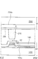
Fig. 3 and Fig. 4 are respectively the cross-sectional views along the line III-III of Fig. 2 and IV-IV extraction.
With reference to Fig. 3 and Fig. 4, the IPS-LCD device 10 of prior art comprises array base palte, colour filtering chip basic board and the liquid crystal layer between two substrates.
The grid line 52 and the first concentric line 56a are arranged on first substrate 50.On the grid line 52 and the first concentric line 56a, gate insulation layer GI is arranged.Semiconductor layer 60 is arranged on gate insulation layer GI, source electrode 62 and drain electrode 64 are arranged on semiconductor layer 60.Semiconductor layer 60 comprises active layer 60a and ohmic contact layer 60b.Gate insulation layer GI is provided with height adjuster 86, and it is corresponding to grid line 52.Height adjuster 86 comprises semiconductor pattern 86a and metal pattern 86b.Source electrode 62 and drain electrode 64 and height adjuster 86 are provided with passivation layer.Thin film transistor (TFT) T comprises grid 54, semiconductor layer 60 and source electrode 62 and drains 64.Grid line 52 and data line (Fig. 2 72) limit pixel region P.
For this difference in height, height adjuster 86 is set at array base palte place corresponding to gap wadding 98a.
The grid line 52 and the first concentric line 56a have approximately
 To about
 Thickness, gate insulation layer GI has approximately
 Thickness,
 semiconductor layer 60 has approximately
 Thickness, source electrode and drain electrode have approximately
 Thickness.Be approximately corresponding to the array base palte of
 gap wadding 98a and corresponding to the difference in height between the array base palte of slow pressure wadding 98b
 This difference in height is quite big.Yet, when taking turns mask process manufacturing array substrate, because
 metal pattern 86b covers semiconductor pattern 86a, so reduced this difference in height to a certain extent by five.Therefore, can reduce by contacting the defective that is caused with liquid crystal panel.
Yet as mentioned above, the IPS-LCD device of prior art needs five to take turns mask process, thereby has increased cost and manufacturing time.
Summary of the invention
Therefore, the present invention relates to a kind of liquid crystal display device and manufacture method thereof, it has overcome substantially because the restriction of prior art and one or more problems that shortcoming causes.
Advantage of the present invention has provided a kind of liquid crystal display device and manufacture method thereof, and it has reduced manufacturing cost and manufacturing time.
Other feature and advantage of the present invention will be listed in the following description, and wherein a part becomes apparent from following description, perhaps is appreciated that by practice of the present invention.Can realize and obtain purpose of the present invention and other advantage by the structure that in writing instructions and claims and accompanying drawing, particularly points out.
For the advantage that realizes these purposes and other and according to purpose of the present invention, as specializing here and broadly described, a kind of liquid crystal display device comprises array base palte, and it comprises: grid line on first substrate and concentric line, and concentric line and grid line are spaced apart; Gate insulation layer on concentric line and grid line; On described gate insulation layer and with described grid line, intersect to limit the data line of pixel region; With the thin film transistor (TFT) that grid line is connected with data line, described thin film transistor (TFT) comprises semiconductor layer and source electrode on described semiconductor layer and the drain electrode on grid, the gate insulation layer; With first and second height adjusters, described first height adjuster is in grid line and concentric line on the gate insulation layer above at least one, described second height adjuster is on the gate insulation layer between first concentric line of grid line and concentric line, each all has semiconductor pattern and conductive pattern described first height adjuster and described second height adjuster, and it is formed by the material identical materials with semiconductor layer and source electrode and drain electrode respectively; Relative substrate in the face of array base palte; Liquid crystal layer between array base palte and relative substrate; Corresponding to first height adjuster and with the gap wadding of array base palte and relative substrate contacts; Corresponding to second height adjuster, with relative substrate contacts and with the slow wadding of pressing of array base palte isolated first; Press wadding with delaying with relative substrate contacts and with array base palte isolated second, the described second slow wadding of pressing is corresponding with described concentric line; Wherein the distance between the first slow pressure wadding and the array base palte is roughly less than the second slow distance of pressing between wadding and the array base palte.
In another aspect, a kind of method of making liquid crystal display device comprises: form array base palte, comprising: form grid line and grid on first substrate; On grid line and grid, form gate insulation layer; With on gate insulation layer, form with the grid line data line crossing to limit pixel region, on grid, form semiconductor layer and source electrode and drain electrode, and form first and second height adjusters; Form relative substrate in the face of array base palte; Form the gap wadding and the first and second slow waddings of pressing with relative substrate contacts, its intermediate gap wadding contacts corresponding to first height adjuster and with array base palte, the first slow wadding of pressing is corresponding to second height adjuster, and the distance between the first slow pressure wadding and the array base palte is roughly less than the second slow distance of pressing between wadding and the array base palte; And between array base palte and relative substrate the clamping liquid crystal layer.
In another aspect, a kind of liquid crystal display device comprises array base palte, and it comprises intersected with each other to limit the grid line and the data line of pixel region; Relative substrate in the face of array base palte; Liquid crystal layer between array base palte and relative substrate; Gap wadding with array base palte and relative substrate contacts; Contact with in array base palte and the relative substrate one and with array base palte and another isolated first slow wadding of pressing in the substrate relatively; With with array base palte and relative substrate in one contact and with array base palte and another isolated second slow wadding of pressing in the substrate relatively, wherein first slow press in wadding and array base palte and the subtend substrate and the first slow isolated described distance between another of wadding of pressing is roughly slowly pressed in wadding and array base palte and the subtend substrate and second delayed the isolated distance between another of pressure wadding less than second.
The generality that should be appreciated that front of the present invention describe and following detailed all be typicalness with indicative, be intended to provide the present invention described in claim further to explain.
Description of drawings
Illustrate embodiment of the present invention and be used from explanation principle of the present invention to the accompanying drawing that the invention provides a further understanding and a composition instructions part with instructions one.
In the accompanying drawings:
Fig. 1 is the skeleton view of diagram according to the LCD device of prior art;
Fig. 2 is the planimetric map of diagram according to the IPS-LCD device of prior art;
Fig. 3 and Fig. 4 are respectively the cross-sectional views along the line III-III of Fig. 2 and IV-IV extraction;
Fig. 5 is the planimetric map according to the IPS-LCD device of embodiment of the present invention;
Fig. 6 is respectively line V-V along Fig. 5 to Fig. 8, the cross-sectional view that VI-VI and VII-VII extract;
Fig. 9 A to 9H, 10A to 10H, 11A is respectively the cross-sectional view that line V-V, VI-VI, VII-VII and VIII-VIII along Fig. 5 extract to 11H and 12A to 12H, it illustrates the method for making the IPS-LCD device according to embodiment of the present invention; With
Figure 13 A is the cross-sectional view of diagram according to the method for the colour filtering chip basic board of embodiment of the present invention manufacturing IPS-LCD device to 13C.
Embodiment
Describe in detail now with reference to the preferred embodiments of the invention, illustrate embodiment in the accompanying drawing.
Fig. 5 is the planimetric map according to the IPS-LCD device of embodiment of the present invention.
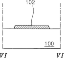
With reference to Fig. 5, in the array base palte according to the IPS-LCD device of embodiment of the present invention, the grid line 102 and the first and second concentric line 106a and 106b extend at substrate 100 upper edge first directions.Extend with the second direction that first direction intersects on data line 130 edges.The semiconductor pattern 122b of data line 130 belows extends along the bearing of trend of data line 130.Grid line 102 and data line 130 limit pixel region P.
Thin film transistor (TFT) T is positioned at the place, point of crossing of grid line 102 and data line 130.Thin film transistor (TFT) T comprises grid 104, semiconductor layer 136 and source electrode 132 and drains 134.Semiconductor pattern 122b extends from semiconductor layer 136.
First public electrode 108 is positioned at the side of pixel region P and is connected with 106b with the first and second concentric line 106a.Second public electrode 150 is connected with the second concentric line 106b by public contact hole 143.Pixel electrode 148 is connected with drain electrode 134 by coupling part 146.Second public electrode 150 and pixel electrode 148 are arranged alternately in pixel region P, thereby produce the copline electric field.Outermost second public electrode 150 roughly with first public electrode, 108 crossovers.Because first public electrode and outermost second public electrode 150 are positioned at the outside of pixel electrode 148, so reduced the coupling between data line 130 and the pixel electrode 148.
The coupling part 146 and the first concentric line 106a be crossover each other, thereby forms memory capacitance Cst.
The colour filtering chip basic board (not shown) is in the face of array base palte.On colour filtering chip basic board, be formed with the gap wadding 208 and the first and second slow waddings 210 and 212 of pressing.Gap wadding 208 is used to keep the box gap between array base palte and the colour filtering chip basic board.The first and second slow waddings 210 and 212 of pressing are kept out the power that imposes on liquid crystal panel from the outside, point the contact liquid crystal panel as the user.
Fig. 6 is respectively line V-V along Fig. 5 to Fig. 8, the cross-sectional view that VI-VI and VII-VII extract.
To Fig. 8, comprise liquid crystal layer between array base palte B2, colour filtering chip basic board B1 and two substrate B1 and the B2 with reference to Fig. 6 according to the IPS-LCD device of embodiment of the present invention.
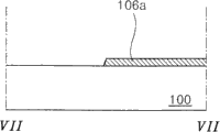
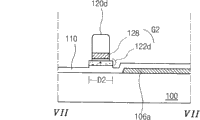
The first height adjuster G1 is arranged on grid line 102, the first concentric line 106a or second concentric line (106b of Fig. 5) top, for example is arranged on the gate insulation layer 110 of grid line 102 tops.The second height adjuster G2 is arranged on the gate insulation layer 110 of the position that does not form grid line 102 and the first and second concentric line 106a and 106b, for example is arranged between the grid line 102 and the first concentric line 106a.
Each first and second height adjuster G1 and G2 comprise semiconductor pattern with intrinsic amorphous silicon pattern and doping amorphous silicon pattern and the conductive pattern that is provided with continuously.The first and second height adjuster G1 and G2 have roughly the same thickness.
Levelling blanket 206 is provided with the gap wadding 208 and the first and second slow waddings 210 and 212 of pressing.The gap wadding 208 and the first and second slow waddings 210 and 212 of pressing have roughly the same thickness.
Array base palte height corresponding to gap wadding 208 roughly is higher than corresponding to the first slow array base palte height of pressing wadding 210.Roughly be higher than corresponding to the second slow array base palte height of pressing wadding 212 corresponding to the first slow array base palte height of wadding 210 of pressing.Therefore, gap wadding 208 contacts with colour filtering chip basic board B1 with array base palte B2.Distance between the first slow pressure wadding 210 and the array base palte B2 is roughly less than the second slow distance of pressing between wadding 212 and the array base palte B2.
With the array base palte of four-wheel mask process manufacturing according to the IPS-LCD device of embodiment of the present invention.In identical mask process, use dry ecthing to form semiconductor layer 136 and source electrode 132 and drain electrode 134.In dry etch process, part removes gate insulation layer 110, and roughly reduces the thickness of gate insulation layer 110.Therefore, compare, also roughly reduced corresponding to the second slow array base palte height of pressing wadding 212 with the array base palte of prior art.For example, be approximately corresponding to the array base palte of gap wadding 208 and corresponding to the difference in height between the array base palte of the second slow pressure wadding 212
 The increase of difference in height reduced second slow press wadding 212 subtract the power function.In order to compensate second slow reducing of wadding function, the formation first
 slow wadding 210 and the second height adjuster G2 of pressing in the IPS-LCD device of pressing.
When applying external force, the first slow wadding 210 of pressing alleviates external force earlier, and the second slow wadding 212 of pressing alleviates external force once more.Therefore, roughly be higher than corresponding to the second slow array base palte height of pressing wadding 212 corresponding to the first slow array base palte height of wadding 210 of pressing.Like this, the formation second height adjuster G2 below the first slow pressure wadding 210.Should be corresponding to the first slow array base palte height of wadding 210 of pressing roughly less than array base palte height corresponding to gap wadding 208.Like this, in the zone of the second height adjuster G2 between the grid line 102 and the first concentric line 106a.Therefore, be approximately the thickness of grid line 102 or concentric line 106a or 106b, promptly be approximately 2000 to approximately corresponding to the array base palte of gap wadding 208 and corresponding to the difference in height between the first slow array base palte of pressing wadding 210
 This difference in height has compensated corresponding to the array base palte of
 gap wadding 208 and corresponding to the difference in height between the array base palte of the second slow pressure wadding 212.
When the second height adjuster G2 regional between the grid line 102 and the first concentric line 106a, the zone between the grid line 102 and the first concentric line 106a may be enough big to hold the second height adjuster G2 in this zone.In other words, the first slow area of wadding 210 of pressing is greater than available zone.When this zone was enough not big, the grid line 102 and/or the first concentric line 106a had inside recess, to hold the second height adjuster G2, as shown in Figure 5.
As mentioned above, by forming first and second height adjusters and regulating corresponding to the gap wadding and the first and second slow height of pressing the array base palte of wadding by the position of regulating first and second height adjusters.In other words, the gap wadding and the second slow wadding of pressing are arranged on grid line and concentric line top, but by below the wadding of gap, forming first height adjuster, roughly be higher than corresponding to the second slow array base palte height of pressing wadding corresponding to the array base palte height of wadding.First and second height adjusters are arranged on the gap wadding and first slow the pressure below the wadding, but by forming first height adjuster in the position that is formed with grid line and form second height adjuster, roughly be higher than corresponding to the first slow array base palte height of pressing wadding corresponding to the array base palte height of gap wadding in the position that does not form grid line or concentric line.
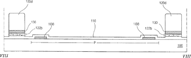
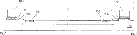
Fig. 9 A to 9H, 10A to 10H, 11A is respectively the cross-sectional view that line V-V, VI-VI, VII-VII and VIII-VIII along Fig. 5 extract to 11H and 12A to 12H, illustrates the method for making the IPS-LCD device according to embodiment of the present invention.
With reference to Fig. 9 A, 10A, 11A and 12A, deposits conductive material on substrate 100 with pixel region P and switch region S, and with first mask process to its composition, thereby form grid line 102, grid 104, the first concentric line 106a, second concentric line (106b of Fig. 5) and first public electrode 108.Conductive material comprises aluminium (Al), aluminium neodymium alloy (AlNd), chromium (Cr), tungsten (W), molybdenum (Mo) and titanium (Ti).The grid line 102 and/or the first concentric line 106a comprise recess, as shown in Figure 5.
With reference to Fig. 9 B, 10B, 11B and 12B, on substrate 100, form gate insulation layer 110, intrinsic amorphous si-layer 112, doping amorphous si-layer 114 and conductive layer 116 continuously with grid line 102.On conductive layer 116, form photoresist layer 118.Gate insulation layer 110 comprises monox (SiO
2) and silicon nitride (SiN
x).Conductive layer 116 comprises aluminium (Al), aluminium neodymium alloy (AlNd), chromium (Cr), tungsten (W), molybdenum (Mo) and titanium (Ti).
On photoresist layer 118, place mask M with transmission part B1, stop portions B2 and half transmitting part B3.Half transmitting part B3 comprises semi-transmissive film or slit pattern.
Half transmitting part B3 is corresponding to a part of grid 104.Stop portions B2 is arranged on the both sides of half transmitting part B3.Stop portions B2 is arranged on the both sides of pixel region P.Stop portions B2 is arranged on the first area D1 in the grid line 102.Stop portions B2 is arranged on the second area D2 between the grid line 02 and the first concentric line 106a.By mask M photoresist layer 118 is exposed and development.
With reference to Fig. 9 C, 10C, 11C and 12C,, form first to the 4th photoresist pattern 120a to 120d by exposure and development.The first photoresist pattern 120a is corresponding to switch region S.The second photoresist pattern 120b is corresponding to pixel region P both sides.The 3rd photoresist pattern 120c is corresponding to first area D1.The 4th photoresist pattern 120d is corresponding to second area D2.Use first to the 4th photoresist pattern 120a to 120d etching conductive layer 116, intrinsic amorphous si-layer 114 and doping amorphous silicon 112.Roughly thin corresponding to the part of the first photoresist pattern 120a of half transmitting part (B3 of Fig. 9 B) than other parts corresponding to the first photoresist pattern 120a of stop portions (B2 of Fig. 9 B).
With reference to Fig. 9 D, 10D, 11D and 12D,, below the first photoresist pattern 120a, form the source-drain pattern 124 and the first semiconductor pattern 122a by etching.Below the second photoresist pattern 120b, form the data line 130 and the second semiconductor pattern 122b.Below the 3rd photoresist pattern 120c, form the first height adjuster G1 with first conductive pattern 126 and the 3rd semiconductor pattern 122c.Below the 4th photoresist pattern 120d, form the second height adjuster G2 with second conductive pattern 128 and the 4th semiconductor pattern 122d.
In etching process, also partly etching first to the 4th photoresist pattern 120a to the gate insulation layer between the 120d 110.
With reference to Fig. 9 E, 10E, 11E and 12E, ashing first to the 4th photoresist pattern 120a is to 120d.By ashing, part removes first to the 4th photoresist pattern 120a to 120d.Carry out ashing until thoroughly removed the first photoresist pattern (120a of Fig. 9 D) part with low thickness.Therefore, exposed the center of source-drain pattern 124.In addition, also exposed the sidepiece of source-drain pattern 124, data line 130 and first and second conductive patterns 126 and 128.
With reference to Fig. 9 F, 10F, 11F and 12F, use first to the 4th photoresist pattern 120a of ashing to carry out etching work procedure to 120d.By etching, remove the center of the doping amorphous si-layer of source-drain pattern (Fig. 9 E 124) and first semiconductor pattern (122a of Fig. 9 E), thereby form source electrode 132 and drain electrode 134 and ohmic contact layer 138.The intrinsic amorphous si-layer of first semiconductor pattern is called active layer 137.In addition, remove the sidepiece of the doping amorphous si-layer of the source-drain pattern and first semiconductor pattern.Also removed data line 130, first and second conductive patterns 126 and the 128 and second to the 4th semiconductor pattern 122b sidepiece to the doping amorphous si-layer of 122d.
In etching process, also part has removed the gate insulation layer 110 between first to the 4th semiconductor pattern.First to the 4th photoresist pattern 120a that peels off ashing is to 120d.
By Fig. 9 B to 9F, 10B to 10F, second mask process of 11B to 11F and 12B to 12F, the gate insulation layer 110 between twice partially-etched first to the 4th semiconductor pattern.By twice etching, the thickness of the gate insulation layer 110 between first to the 4th semiconductor pattern has reduced approximately

With reference to Fig. 9 G, 10G, 11G and 12G, on substrate 100, form passivation layer 140 with data line 130.With the 3rd mask process etch passivation layer 140, thereby form to expose the drain contact hole 142 of drain electrode 134 and expose the public contact hole (Fig. 5 143) of second concentric line (106b of Fig. 5).Passivation layer 140 is formed by organic insulation or inorganic insulating material.Organic insulation comprises benzocyclobutene (BCB) and acryl resin, and inorganic insulating material comprises silicon dioxide (SiO
2) and silicon nitride (SiN
x).
With reference to Fig. 9 H, 10H, 11H and 12H, deposit transparent conductive material on passivation layer 140, and with the 4th mask process to its composition, thereby form pixel electrode 148, second public electrode 150 and coupling part 146.Connecting portion 146 contacts with drain electrode 134 by drain contact hole 142, and second public electrode 150 contacts with second concentric line by public contact hole.Transparent conductive material comprises tin indium oxide (ITO) and indium zinc oxide (IZO).
By top four-wheel mask process, made array base palte according to embodiment of the present invention.
Figure 13 A is the cross-sectional view of diagram according to the method for the colour filtering chip basic board of embodiment of the present invention manufacturing IPS-LCD device to 13C.
With reference to Figure 13 A, on substrate 200, form black matrix" 202.Black matrix" 202 is arranged on the periphery of pixel region P.Black matrix" 202 comprises chromium (Cr) and chromium oxide (CrO
2).Form redness, green and blue color filter pattern 204a and 204b corresponding to each pixel region P.
With reference to Figure 13 B, on substrate 200, deposit organic insulation, thereby form levelling blanket 206 with color filter pattern 204a and 204b.Organic material comprises benzocyclobutene (BCB) and acryl resin.
With reference to Figure 13 C, deposition organic insulation and on levelling blanket 206 to its composition, thus form the gap wadding 208 and the first and second slow waddings (210 and Fig. 6 of Fig. 8 212) of pressing.Organic material comprises benzocyclobutene (BCB) and acryl resin.
By above-mentioned operation, made colour filtering chip basic board according to embodiment of the present invention.
With between accompany liquid crystal layer mode with array base palte and colour filtering chip basic board bonding, thereby finish the IPS-LCD device.
As mentioned above, because with four-wheel mask process manufacturing array substrate, so can reduce manufacturing cost and manufacturing time.In addition, compensate the second slow pressure wadding because form the first slow wadding of pressing, so reduced because the decline of the display quality that external force causes.In addition, because public electrode and pixel electrode are transparent, obtained high brightness.In addition, because public electrode is arranged on the pixel region side, so reduced the coupling between data line and the pixel electrode.
The present invention is not only applicable to IPS mode LCD device, but also is applicable to the LCD device of other various patterns.
Under the situation that does not break away from the spirit or scope of the present invention, the present invention can do various modifications and variations, and this it will be apparent to those skilled in the art that.Thereby, the invention is intended to cover the modifications and variations of the present invention that fall in claims and the equivalent scope thereof.
Claims (15)
1. liquid crystal display device comprises:
Array base palte, it comprises:
Grid line on first substrate and concentric line, concentric line and grid line are spaced apart;
Gate insulation layer on concentric line and grid line;
On described gate insulation layer and with described grid line, intersect to limit the data line of pixel region;
With the thin film transistor (TFT) that grid line is connected with data line, described thin film transistor (TFT) comprises semiconductor layer and source electrode on described semiconductor layer and the drain electrode on grid, the gate insulation layer; With
First and second height adjusters, described first height adjuster is in grid line and concentric line on the gate insulation layer above at least one, described second height adjuster is on the gate insulation layer between first concentric line of grid line and concentric line, each all has semiconductor pattern and conductive pattern described first height adjuster and described second height adjuster, and it is formed by the material identical materials with semiconductor layer and source electrode and drain electrode respectively;
Relative substrate in the face of array base palte;
Liquid crystal layer between array base palte and relative substrate;
Corresponding to first height adjuster and with the gap wadding of array base palte and relative substrate contacts;
Corresponding to second height adjuster, with relative substrate contacts and with the slow wadding of pressing of array base palte isolated first; With
Delay the pressure wadding with relative substrate contacts and with array base palte isolated second, the described second slow wadding of pressing is corresponding with described concentric line;
Wherein the distance between the first slow pressure wadding and the array base palte is roughly less than the second slow distance of pressing between wadding and the array base palte.
2. device according to claim 1 is characterized in that, described semiconductor layer comprises intrinsic amorphous si-layer and the doping amorphous si-layer on this intrinsic amorphous si-layer.
3. device according to claim 1 is characterized in that described semiconductor layer extends below data line.
4. device according to claim 2 is characterized in that, described intrinsic amorphous si-layer is projected into doping amorphous si-layer outside.
5. device according to claim 1 is characterized in that, described semiconductor layer and source electrode and drain electrode are as first height adjuster.
6. device according to claim 1 is characterized in that, further is included in the pixel electrode and second public electrode that are arranged alternately in the pixel region, and wherein pixel electrode is connected with thin film transistor (TFT), and second public electrode is connected with concentric line.
7. device according to claim 6 is characterized in that described concentric line further comprises second concentric line, and described first and second concentric lines connect by first public electrode of pixel electrode outside, and second concentric line is connected with second public electrode.
8. device according to claim 7 is characterized in that, described first public electrode roughly with the second public electrode crossover, second public electrode is positioned at identical with pixel electrode layer, and first public electrode extends from first and second concentric lines.
9. device according to claim 7, it is characterized in that, further comprise passivation layer, this passivation layer has drain contact hole and public contact hole together with gate insulation layer, pixel electrode is connected with thin film transistor (TFT) by the drain contact hole, and second public electrode is connected with second concentric line by public contact hole.
10. device according to claim 1 is characterized in that, described relative substrate is included in black matrix", color filter layer and the levelling blanket on second substrate.
11. device according to claim 1, it is characterized in that, array base palte part corresponding to the gap wadding roughly is higher than corresponding to the first slow array base palte part of pressing wadding, and roughly is higher than corresponding to the second slow array base palte part of pressing wadding corresponding to the first slow array base palte part of wadding of pressing.
12. device according to claim 11 is characterized in that, the described gap wadding and the first and second slow waddings of pressing have roughly the same thickness.
13. device according to claim 11 is characterized in that, described first and second height adjusters have roughly the same thickness.
14. device according to claim 1 is characterized in that, is approximately corresponding to the array base palte part of gap wadding and corresponding to the difference in height between the array base palte part of the first slow pressure wadding

15. device according to claim 1 is characterized in that, the gate insulation layer below first and second height adjusters partly slow presses the gate insulation layer part below the wadding thick approximately than second

Applications Claiming Priority (2)
| Application Number | Priority Date | Filing Date | Title |
|---|---|---|---|
| KR1020060041835 | 2006-05-10 | ||
| KR1020060041835A KR100920481B1 (en) | 2006-05-10 | 2006-05-10 | In Plane Switching mode LCD and method of fabricating of the same |
Publications (2)
| Publication Number | Publication Date |
|---|---|
| CN101071241A CN101071241A (en) | 2007-11-14 |
| CN100559249C true CN100559249C (en) | 2009-11-11 |
Family
ID=38684774
Family Applications (1)
| Application Number | Title | Priority Date | Filing Date |
|---|---|---|---|
| CNB2006101680525A Active CN100559249C (en) | 2006-05-10 | 2006-12-15 | Liquid crystal display device and manufacture method thereof |
Country Status (4)
| Country | Link |
|---|---|
| US (2) | US7920244B2 (en) |
| JP (1) | JP4571615B2 (en) |
| KR (1) | KR100920481B1 (en) |
| CN (1) | CN100559249C (en) |
Families Citing this family (20)
| Publication number | Priority date | Publication date | Assignee | Title |
|---|---|---|---|---|
| KR20070071783A (en) * | 2005-12-30 | 2007-07-04 | 엘지.필립스 엘시디 주식회사 | Lcd and method of fabricating of the same |
| US7894024B2 (en) | 2007-07-26 | 2011-02-22 | Beijing Boe Optoelectronics Technology Co., Ltd. | Liquid crystal panel |
| CN100595654C (en) * | 2007-12-29 | 2010-03-24 | 昆山龙腾光电有限公司 | Liquid crystal display panel |
| TWI385568B (en) * | 2009-02-24 | 2013-02-11 | Au Optronics Corp | Display apparatus and touch detection method |
| JP2010237503A (en) * | 2009-03-31 | 2010-10-21 | Hitachi Displays Ltd | Liquid crystal display |
| KR101621027B1 (en) | 2009-12-30 | 2016-05-16 | 삼성디스플레이 주식회사 | Display apparatus and method for manufacturing the same |
| KR101681923B1 (en) * | 2010-09-01 | 2016-12-02 | 엘지디스플레이 주식회사 | Liquid Crystal Display Device and Method for fabricating the same |
| KR101730995B1 (en) * | 2010-10-22 | 2017-04-28 | 삼성디스플레이 주식회사 | Display apparatus |
| KR101888033B1 (en) * | 2011-08-04 | 2018-09-10 | 엘지디스플레이 주식회사 | In-Plane switching mode liquid crystal display device |
| KR101420686B1 (en) * | 2011-11-17 | 2014-07-21 | 엘지디스플레이 주식회사 | Image display device including barrier cell and method of fabricating the same |
| CN102591048A (en) * | 2012-03-26 | 2012-07-18 | 深圳市华星光电技术有限公司 | Liquid crystal display panel, manufacturing method for same and liquid crystal display device |
| US9349753B2 (en) * | 2014-02-24 | 2016-05-24 | Boe Technology Group Co., Ltd. | Array substrate, method for producing the same and display apparatus |
| JP6401923B2 (en) | 2014-03-20 | 2018-10-10 | 株式会社ジャパンディスプレイ | Liquid crystal display |
| CN104977749A (en) * | 2015-07-28 | 2015-10-14 | 京东方科技集团股份有限公司 | Color film substrate, manufacturing method thereof, and display device |
| CN105301858B (en) * | 2015-11-06 | 2018-09-18 | 深圳市华星光电技术有限公司 | The preparation method and array substrate of a kind of display panel, display panel |
| JP6367395B2 (en) * | 2017-02-14 | 2018-08-01 | 株式会社ジャパンディスプレイ | Liquid crystal display |
| JP7011413B2 (en) * | 2017-07-06 | 2022-01-26 | 株式会社ジャパンディスプレイ | Liquid crystal display and electronic devices |
| JP6909713B2 (en) * | 2017-11-16 | 2021-07-28 | パナソニック液晶ディスプレイ株式会社 | Liquid crystal display panel |
| CN110456576B (en) * | 2018-05-08 | 2022-05-13 | 群创光电股份有限公司 | Display device |
| CN108761856B (en) * | 2018-05-17 | 2021-04-20 | 昆山龙腾光电股份有限公司 | Array substrate, liquid crystal display device and driving method |
Family Cites Families (15)
| Publication number | Priority date | Publication date | Assignee | Title |
|---|---|---|---|---|
| JP3680730B2 (en) * | 2000-12-08 | 2005-08-10 | 株式会社日立製作所 | Liquid crystal display |
| JP2002341354A (en) | 2001-05-16 | 2002-11-27 | Matsushita Electric Ind Co Ltd | Liquid crystal display element |
| JP3696127B2 (en) | 2001-05-21 | 2005-09-14 | シャープ株式会社 | Manufacturing method of matrix substrate for liquid crystal |
| JP3946498B2 (en) * | 2001-11-19 | 2007-07-18 | シャープ株式会社 | LCD panel |
| CN1497299A (en) | 2002-09-26 | 2004-05-19 | 三星电子株式会社 | Liquid crystal display, liquid crystal display panel and its making method |
| KR100560401B1 (en) | 2003-11-04 | 2006-03-14 | 엘지.필립스 엘시디 주식회사 | Thin film transistor substrate of horizontal electronic field applying type and fabricating method thereof |
| KR101035847B1 (en) | 2003-07-03 | 2011-05-19 | 삼성전자주식회사 | Liquid crystal display panel |
| JP4583015B2 (en) | 2003-09-29 | 2010-11-17 | 三洋電機株式会社 | Character display control circuit and integrated circuit |
| KR20050039981A (en) * | 2003-10-27 | 2005-05-03 | 엘지.필립스 엘시디 주식회사 | In-plane switching mode liquid crystal display device |
| JP2005189662A (en) | 2003-12-26 | 2005-07-14 | Fujitsu Display Technologies Corp | Liquid crystal display and its manufacturing method |
| KR100672651B1 (en) * | 2004-02-25 | 2007-01-24 | 엘지.필립스 엘시디 주식회사 | Liquid Crystal Display Device and method for manufacturing the same |
| KR100617039B1 (en) * | 2004-02-26 | 2006-08-30 | 엘지.필립스 엘시디 주식회사 | Liquid Crystal Display Device and method for Manufacturing the same |
| KR100641002B1 (en) * | 2004-04-30 | 2006-11-02 | 엘지.필립스 엘시디 주식회사 | Liquid Crystal Display Device |
| CN2699333Y (en) | 2004-05-10 | 2005-05-11 | 友达光电股份有限公司 | High-pressure withstanding mixed type spacing wall construction |
| KR101085149B1 (en) * | 2004-10-08 | 2011-11-21 | 엘지디스플레이 주식회사 | Liquid Crystal Display Device and Method for Manufacturing the Same |
-
2006
- 2006-05-10 KR KR1020060041835A patent/KR100920481B1/en active IP Right Grant
- 2006-12-14 US US11/638,385 patent/US7920244B2/en active Active
- 2006-12-15 CN CNB2006101680525A patent/CN100559249C/en active Active
- 2006-12-22 JP JP2006345351A patent/JP4571615B2/en active Active
-
2011
- 2011-01-21 US US13/011,222 patent/US8325314B2/en active Active
Also Published As
| Publication number | Publication date |
|---|---|
| JP2007304556A (en) | 2007-11-22 |
| KR100920481B1 (en) | 2009-10-08 |
| US20070263162A1 (en) | 2007-11-15 |
| CN101071241A (en) | 2007-11-14 |
| US7920244B2 (en) | 2011-04-05 |
| US8325314B2 (en) | 2012-12-04 |
| JP4571615B2 (en) | 2010-10-27 |
| KR20070109202A (en) | 2007-11-15 |
| US20110136274A1 (en) | 2011-06-09 |
Similar Documents
| Publication | Publication Date | Title |
|---|---|---|
| CN100559249C (en) | Liquid crystal display device and manufacture method thereof | |
| US6747712B2 (en) | Fringe field switching liquid crystal display device and method for manufacturing the same | |
| US8670098B2 (en) | Liquid crystal display panel and manufacturing method of the same | |
| US7538827B2 (en) | Pixel structure | |
| US7473926B2 (en) | Array substrate for liquid crystal display device and method of fabricating the same | |
| US7916229B2 (en) | Liquid crystal display device and method for fabricating the same | |
| US7701521B2 (en) | Array substrate having particular storage capacitance structure for liquid crystal display device and method of manufacturing the same | |
| US7170571B2 (en) | Liquid crystal display device with double metal layer source and drain electrodes and fabricating method thereof | |
| CN102116981B (en) | Thin film transistor array substrate and method for fabricating the same | |
| CN101169565A (en) | Array substrate for liquid crystal display device and method of fabricating the same | |
| KR20110007964A (en) | Tft-lcd array substrate and method of fabricating the same | |
| US8045081B2 (en) | Liquid crystal display device with photosensor and method of fabricating the same | |
| US7525624B2 (en) | Liquid crystal display device and fabricating method thereof | |
| US7459725B2 (en) | Thin film transistor array substrate and fabrication method thereof | |
| CN103137555B (en) | Thin film transistor LCD device and manufacture method thereof | |
| CN101071218B (en) | Liquid crystal display device | |
| US8243222B2 (en) | Array substrate for liquid crystal display device and method of manufacturing the same | |
| US6862049B2 (en) | Liquid crystal display device with minimum OHMIC contact between reflective and transparent electrodes | |
| US20050094046A1 (en) | Liquid crystal display device and method for fabricating the same | |
| US6432734B1 (en) | Method of manufacturing a display unit of a flat display panel having a wide viewing angle | |
| US8299468B2 (en) | Display substrate having reduced defects | |
| US7589030B2 (en) | Liquid crystal display device and fabricating method thereof | |
| CN219759589U (en) | Thin film transistor array substrate, liquid crystal display panel and device | |
| JPH07294960A (en) | Tft type liquid crystal display device | |
| TW200410416A (en) | Thin film transistor substrate for liquid crystal display(LCD) and method of manufacturing the same |
Legal Events
| Date | Code | Title | Description |
|---|---|---|---|
| C06 | Publication | ||
| PB01 | Publication | ||
| C10 | Entry into substantive examination | ||
| SE01 | Entry into force of request for substantive examination | ||
| C14 | Grant of patent or utility model | ||
| GR01 | Patent grant |