CN100557075C - Handle the method for substrate - Google Patents
Handle the method for substrate Download PDFInfo
- Publication number
- CN100557075C CN100557075C CNB2005800100297A CN200580010029A CN100557075C CN 100557075 C CN100557075 C CN 100557075C CN B2005800100297 A CNB2005800100297 A CN B2005800100297A CN 200580010029 A CN200580010029 A CN 200580010029A CN 100557075 C CN100557075 C CN 100557075C
- Authority
- CN
- China
- Prior art keywords
- substrate
- metal
- gas
- exposed
- well heater
- Prior art date
- Legal status (The legal status is an assumption and is not a legal conclusion. Google has not performed a legal analysis and makes no representation as to the accuracy of the status listed.)
- Active
Links
Images


Classifications
-
- C—CHEMISTRY; METALLURGY
- C23—COATING METALLIC MATERIAL; COATING MATERIAL WITH METALLIC MATERIAL; CHEMICAL SURFACE TREATMENT; DIFFUSION TREATMENT OF METALLIC MATERIAL; COATING BY VACUUM EVAPORATION, BY SPUTTERING, BY ION IMPLANTATION OR BY CHEMICAL VAPOUR DEPOSITION, IN GENERAL; INHIBITING CORROSION OF METALLIC MATERIAL OR INCRUSTATION IN GENERAL
- C23C—COATING METALLIC MATERIAL; COATING MATERIAL WITH METALLIC MATERIAL; SURFACE TREATMENT OF METALLIC MATERIAL BY DIFFUSION INTO THE SURFACE, BY CHEMICAL CONVERSION OR SUBSTITUTION; COATING BY VACUUM EVAPORATION, BY SPUTTERING, BY ION IMPLANTATION OR BY CHEMICAL VAPOUR DEPOSITION, IN GENERAL
- C23C16/00—Chemical coating by decomposition of gaseous compounds, without leaving reaction products of surface material in the coating, i.e. chemical vapour deposition [CVD] processes
- C23C16/44—Chemical coating by decomposition of gaseous compounds, without leaving reaction products of surface material in the coating, i.e. chemical vapour deposition [CVD] processes characterised by the method of coating
- C23C16/458—Chemical coating by decomposition of gaseous compounds, without leaving reaction products of surface material in the coating, i.e. chemical vapour deposition [CVD] processes characterised by the method of coating characterised by the method used for supporting substrates in the reaction chamber
- C23C16/4581—Chemical coating by decomposition of gaseous compounds, without leaving reaction products of surface material in the coating, i.e. chemical vapour deposition [CVD] processes characterised by the method of coating characterised by the method used for supporting substrates in the reaction chamber characterised by material of construction or surface finish of the means for supporting the substrate
-
- C—CHEMISTRY; METALLURGY
- C23—COATING METALLIC MATERIAL; COATING MATERIAL WITH METALLIC MATERIAL; CHEMICAL SURFACE TREATMENT; DIFFUSION TREATMENT OF METALLIC MATERIAL; COATING BY VACUUM EVAPORATION, BY SPUTTERING, BY ION IMPLANTATION OR BY CHEMICAL VAPOUR DEPOSITION, IN GENERAL; INHIBITING CORROSION OF METALLIC MATERIAL OR INCRUSTATION IN GENERAL
- C23C—COATING METALLIC MATERIAL; COATING MATERIAL WITH METALLIC MATERIAL; SURFACE TREATMENT OF METALLIC MATERIAL BY DIFFUSION INTO THE SURFACE, BY CHEMICAL CONVERSION OR SUBSTITUTION; COATING BY VACUUM EVAPORATION, BY SPUTTERING, BY ION IMPLANTATION OR BY CHEMICAL VAPOUR DEPOSITION, IN GENERAL
- C23C16/00—Chemical coating by decomposition of gaseous compounds, without leaving reaction products of surface material in the coating, i.e. chemical vapour deposition [CVD] processes
- C23C16/06—Chemical coating by decomposition of gaseous compounds, without leaving reaction products of surface material in the coating, i.e. chemical vapour deposition [CVD] processes characterised by the deposition of metallic material
- C23C16/16—Chemical coating by decomposition of gaseous compounds, without leaving reaction products of surface material in the coating, i.e. chemical vapour deposition [CVD] processes characterised by the deposition of metallic material from metal carbonyl compounds
-
- C—CHEMISTRY; METALLURGY
- C23—COATING METALLIC MATERIAL; COATING MATERIAL WITH METALLIC MATERIAL; CHEMICAL SURFACE TREATMENT; DIFFUSION TREATMENT OF METALLIC MATERIAL; COATING BY VACUUM EVAPORATION, BY SPUTTERING, BY ION IMPLANTATION OR BY CHEMICAL VAPOUR DEPOSITION, IN GENERAL; INHIBITING CORROSION OF METALLIC MATERIAL OR INCRUSTATION IN GENERAL
- C23C—COATING METALLIC MATERIAL; COATING MATERIAL WITH METALLIC MATERIAL; SURFACE TREATMENT OF METALLIC MATERIAL BY DIFFUSION INTO THE SURFACE, BY CHEMICAL CONVERSION OR SUBSTITUTION; COATING BY VACUUM EVAPORATION, BY SPUTTERING, BY ION IMPLANTATION OR BY CHEMICAL VAPOUR DEPOSITION, IN GENERAL
- C23C16/00—Chemical coating by decomposition of gaseous compounds, without leaving reaction products of surface material in the coating, i.e. chemical vapour deposition [CVD] processes
- C23C16/44—Chemical coating by decomposition of gaseous compounds, without leaving reaction products of surface material in the coating, i.e. chemical vapour deposition [CVD] processes characterised by the method of coating
- C23C16/458—Chemical coating by decomposition of gaseous compounds, without leaving reaction products of surface material in the coating, i.e. chemical vapour deposition [CVD] processes characterised by the method of coating characterised by the method used for supporting substrates in the reaction chamber
Abstract
The ceramic substrate well heater (20,600,700) that the present invention relates in treatment chamber (10) is gone up the method for handling substrate (25,620,720).Described method comprises: the described ceramic substrate well heater (20,600,700) in described treatment chamber (10) is gone up and is formed supercoat (730,790), and handles substrate (25,620,720) on described coated substrate heater.Described method can comprise pending substrate (25,620,720) be provided on the described coated ceramic substrate well heater, by with described substrate (25,620,720) be exposed in the processing gas described substrate (25,620,720) handle, and described treated substrate is taken out from described treatment chamber (10).
Description
Technical field
The present invention relates to the chamber and handle, more specifically, relate to a kind of method that is used for handling at treatment chamber substrate, this treatment chamber has the ceramic substrate well heater of support substrates.
Background technology
Many semiconducter process carry out in treatment chamber, for example, and plasma etching chamber, plasma deposition chamber, thermal chamber, CVD (Chemical Vapor Deposition) chamber, atomic layer deposition chamber etc.These treatment chambers use the ceramic substrate well heater to come support substrates (for example, wafer) usually and the substrate heat are provided.Generally speaking, the ceramic substrate well heater provides good performance, for example, low heat expansion property, high temperature resistant, low-k, hardness and dimensional stability, these performances make them become the preferred material that is used for many semiconductor application.The ceramic substrate well heater is usually by forming with the metal oxide or the nitride of the powder combinations of glass or frit.The mixing that changes these materials makes change in physical.Mixture is by curtain coating, powder extruding, roll compacting or extrude the desirable shape of formation, then its sintering is formed hard crystalline structure.
The general ceramic material that is used in the ceramic substrate well heater comprises alumina (Al
2O
3), aluminium nitride (AlN), silicon carbide (SiC) and beryllium oxide (BeO).Because good availability, low relatively cost and stable physical properties, alumina are the stupaliths of the most extensive employing.It is easy to be processed to form different shape and at high temperature keeps firm simultaneously, and can obtain with various purity level.Beryllium oxide has the highest thermal conductivity and has some uses required excellent dielectric strength, but only can obtain undersized beryllium oxide, and should be noted that safety when the deleterious beryllium oxide powder of processing.Silicon carbide also is high heat conduction, and it provides the surrogate of aluminium nitride and beryllium oxide, but must be careful when selecting carbofrax material, because along with the increase of temperature, dielectric strength can change.
Aluminium nitride has high thermal conductivity, and this makes, and it is a fabulous selection when needing response fast or high-caliber temperature homogeneity, but because high bake demand and Master Cost, so its processing is very expensive.The aluminium nitride substrate heater is " cleaning " substrate chemically, this chemically " cleaning " substrate satisfy that semi-conductor, medicine and other are very harsh uses required very clean space environment requirement.And, be used in being characterized as of aluminium nitride substrate in the semiconductor processes: rapid heating, be easy to controlled temperature and excellent plasma-resistance.
The processing of the substrate in the treatment chamber of treatment system can cause being exposed on the system component of processing environment and forms material coating.For example, can on the zone that the ceramic substrate well heater is not covered by substrate, form coating.The partial coating of ceramic substrate well heater can cause heater surfaces (heat) divergency to change, and can cause non-uniform temperature and thermal stresses (thermalstressing) in the ceramic substrate well heater.Thermal stresses can cause the physical abuse that can not repair, for example, and the breaking of ceramic heat modulator material.In addition, substrate and substrate heater or contact the back that to cause substrate with material coating on the substrate heater and pollute.For example, the diffusion of copper in silicon device is the pollution problem of known back, still, other metal (for example, ruthenium (Ru)) also can be under neutral temperature and under the bias condition in silicon rapid diffusion.The inventor have realized that need improve one's methods with reduce or suppress above-mentioned with handle substrate during on the ceramic substrate well heater the relevant problem of formation of material coating, guarantee the strict demand of satisfied processing semiconducter substrate simultaneously.
Summary of the invention
The invention provides a kind of method of in treatment chamber, handling one or more substrate with ceramic substrate well heater; described method comprises: form supercoat on the ceramic substrate well heater, and handle the substrate that is supported on the coated ceramic substrate well heater.Processing can comprise: pending substrate is provided on the coated ceramic substrate well heater, substrate is handled and treated substrate is taken out from treatment chamber.Supercoat comprises surface portion, and this surface portion is non-metallic layer or combination metal/non-metal layer, and this surface portion reduces or eliminates being placed on the back pollution of this lip-deep substrate.In exemplary embodiment, supercoat is the Si/Ru coating, and this coating is included in the Ru layer that forms on the ceramic substrate well heater and the Si layer on the Ru layer.
Description of drawings
In the following drawings:
Fig. 1-5 expression is used to carry out the synoptic diagram of the treatment system of the inventive method;
Fig. 6 A-6G is shown schematically in the cross-sectional view of handling ceramic substrate well heater during the substrate;
Fig. 7 A-7K is shown schematically in the cross-sectional view according to ceramic substrate well heater during embodiment of the present invention processing substrate;
Fig. 8 is expression forms the method for supercoat on the ceramic substrate well heater according to embodiment of the present invention a schema;
Fig. 9 is that expression forms supercoat according to embodiment of the present invention and handles the schema of the method for substrate on the ceramic substrate well heater; With
Figure 10 is that expression forms supercoat according to embodiment of the present invention and handles the schema of the method for substrate on the ceramic substrate well heater.
Embodiment
Pointed in the background technology as above invention part, substrate and substrate heater or contact the back pollution that can cause substrate with material coating on substrate heater.And, during handling substrate, on the ceramic substrate well heater, form partial coating can cause the ceramic substrate well heater and above substrate in temperature distributing disproportionation.And the non-uniform temperature in the ceramic substrate well heater can cause the physical abuse to well heater, and for example, stupalith breaks.Yet; the treatment process that addresses these problems is not appeared in the newspapers; this may both be used to protect the ceramic substrate well heater to guarantee to satisfy the semiconductor processes requirement simultaneously owing to be difficult to realize new method, for example, avoided the back pollution (back pollution) of the substrate that contact with the ceramic substrate well heater.
Therefore, the inventor experiment Analysis on the ceramic substrate heater surfaces, form supercoat and contact the method for polluting with the back of reducing substrate with the temperature homogeneity of improving the ceramic substrate well heater and with substrate with supercoat.Because these experiments and analysis, the inventor have been found that form on the ceramic heater surface supercoat for protection thereafter the ceramic substrate well heater during the processing substrate in treatment chamber guarantee to satisfy semiconductor processes simultaneously and require to provide mechanism flexibly.In the present invention, supercoat refers to the coating on the ceramic substrate well heater, and wherein, this coating comprises one deck or more multi-layered differing materials, and comprises that at least the surface portion that substrate is placed on it, this surface portion are non-metallic layer or combination metal/non-metal layer.For example, the Si/Ru protective layer has the Si layer (nonmetal) at Ru layer top.Non-metallic layer is the random layer that does not have metal.Silicon layer and carbon-coating are the examples of non-metallic layer.The adjacent substrate place does not have metal will protect substrate to avoid the back pollution.Bottom Ru metal level provides temperature homogeneity to avoid breakage with further protection well heater.Combination metal/non-metal layer refers to the layer as metal oxide, metal nitride, metal silicide etc.These combination layers can form by following steps: at first form metal level, after this by metal and nonmetal reaction (for example, oxidation, nitrogenize etc.) are transformed this metal level.Replacedly, these combination layers can form by following steps: metal and contain nonmetal be deposited on the substrate heater before or simultaneously, substrate heater is exposed to metallic gas simultaneously and contains in the nonmetallic gas with metal and nonmetal reaction.
When existing, combination metal/non-metal layer can only constitute the surface portion of supercoat or can constitute whole supercoat (comprising surface portion).Replacedly, in another exemplary embodiment of the present invention, combination metal/non-metal layer can be the middle layer between metal back layer and nonmetallic surface part, maybe can be that the surface portion at bottom that forms on the ceramic substrate well heater and non-metallic layer forms on this bottom.In another embodiment of the present invention, supercoat does not comprise combination metal/non-metal layer, but comprises the surface portion of metal level and non-metallic layer at least.
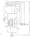
With reference now to accompanying drawing,, Fig. 1 represents that method of the present invention can be carried out at treatment system wherein.Treatment system 1 comprises the treatment chamber 10 (this pedestal is used to install the substrate heater 20 of support and heated substrate 25) with pedestal 5, gas injection system 40 and the vacuum-pumping system 50 that is used for gas 15 is introduced treatment chambers 10.Gas 15 for example can be the reactant gases that is used for forming supercoat on substrate heater 20, maybe can be the processing gas that is used to handle the substrate 25 that is supported by substrate heater 20.Gas injection system 40 independent pilot-gas 15 are from the conveying of strange land source of the gas (not shown) to treatment chamber.Gas can be introduced treatment chamber 10 by gas injection system 40, and adjusts processing pressure.For example, controller 55 is used to control vacuum-pumping system 50 and gas injection system 40.
And substrate heater 20 also can comprise cooling system, and this cooling system comprises from substrate heater 20 reception heats and with the recirculation cooling liquid flowing of transfer of heat to the heat exchange system (not shown).And gas (for example, He) can be sent to the back side of substrate to improve the air gap thermal conduction between substrate 25 and the substrate heater 20.When needs are controlled substrate temperature under high temperature or low temperature, use this system.
Substrate heater can be the ceramic substrate well heater that comprises heating unit 30.Heating unit 30 can be a resistance heating element for example.The ceramic substrate heater material can for example comprise Al
2O
3, AlN, SiC or BeO or the wherein combination of two or more.
Continuation is with reference to figure 1, and gas 15 is introduced treatment zone 60 from gas injection system 40.Gas 15 can be injected high-pressure system (gas injection plenum, not shown), a series of baffle plate (not shown) and porous spray header gas injection plate 65 by gas and introduce treatment zone 60.In one embodiment of the invention, can dispose gas injection system 40 is used for the gas of ald (ALD) technology with promotion Rapid Cycle.Vacuum-pumping system 50 can comprise that pumping speed can and be used for the sluice valve of throttling constant pressure up to the turbomolecular pump (TMP) of 5000l/s (with higher).TMP can be used for low pressure to be handled, and is usually less than 50mTorr.For autoclaving (for example, being higher than 100mTorr), can use mechanical booster pump and dried roughing pump.
In the embodiment depicted in fig. 1, treatment system 1 can for example be used to heat-treat, for example thermal chemical vapor deposition (TCVD) technology or ALD technology.
Fig. 2 represents to be used to carry out the interchangeable treatment system 1 of method of the present invention.Among Fig. 2, treatment system 1 can form and keep plasma body in treatment chamber 10.Plasma process system 1 can for example be used to carry out plasma enhanced chemical vapor deposition technology (PECVD) or plasma etch process.In embodiment shown in Figure 2, substrate heater 20 can also be used as electrode, and by this electrode, radio frequency (RF) power is coupled on the plasma body in the treatment zone 60.For example, RF power is sent to substrate heater 20 from RF producer 45 via impedance matching network 35, can be with the metal electrode (not shown) in the substrate heater at RF voltage place electrical bias.RF biasing is as active electron, thereby and forms and keep plasma body.In this configuration, plasma body is used to deposit a material to substrate 25 (promptly, treatment system 1 can be used as the PECVD reactor) or be used for removing material (that is, treatment system 1 can be used as reactive ion etching (RIE) reactor) from the exposed surface of substrate 25.The typical frequencies of RF biasing be 1MHz to 100MHz, and can be 13.56MHz.
In interchangeable embodiment, RF power can be applied on the substrate heater 20 under the multiple frequency.And impedance matching network 35 will be in the transmission maximization of the RF power in the treatment chamber 10 to plasma body by minimum reflected power.Match network topologies structure (for example, L-type, π-type, T-type) and autocontrol method are as known in the art.Among Fig. 2, controller 55 is coupled with treatment chamber 10, RF producer 45, impedance matching network 35, gas injection system 40, substrate-transfer system 100 and vacuum-pumping system 50, and with they exchange messages.
Fig. 3 represents to be used to carry out another interchangeable treatment system 1 of method of the present invention.The treatment system 1 of Fig. 3 is except those assemblies described in Fig. 2, and the DC field system 70 that also comprises the rotation of machinery or electronics is to increase plasma density potentially and/or to improve the homogeneity of plasma treatment.And controller 55 is coupled in the rotatingfield system 70 to regulate speed of rotation and field intensity.
Fig. 4 represents to be used to carry out another interchangeable plasma process system 1 of method of the present invention.The treatment system 1 of Fig. 4 comprises porous spray header gas injection plate 65, and this injection plate can also be used as the upper board electrode, and RF power is coupled on this plate electrode via impedance matching network 75 from RF producer 80.Be used for the RF power application to the typical frequencies of upper electrode be 10MHz to 200MHz, and can be 60MHz.In addition, be used for the typical frequencies that electric power is applied to lower electrode be 0.1MHz to 30MHz, and can be 2MHz.And controller 55 is coupled on RF producer 80 and the impedance matching network 75 with the application of control RF power to upper electrode 65.
In one embodiment of the invention, the substrate heater among Fig. 4 can be electrical ground.In interchangeable embodiment, the DC biasing can be applied on the substrate heater 20.In another embodiment, substrate heater 20 can with plasma process system 1 electrical isolation.In this scheme, when plasma body is opened, can on substrate heater 20 and substrate 25, form floating potential.
Fig. 5 represents to be used to carry out another treatment system 1 of method of the present invention.The treatment system 1 of improving Fig. 2 is so that further comprise ruhmkorff coil 95, is coupled on this ruhmkorff coil by impedance matching network 90 from the RF power of RF producer 85.RF power is coupled to treatment zone 60 from ruhmkorff coil 95 by the dielectric window (not shown).Be used for the RF power application to the typical frequencies of ruhmkorff coil 80 be 10MHz to 100MHz, and can be 13.56MHz.Similarly, be used for the typical frequencies that electric power is applied to ruhmkorff coil 95 be 10MHz to 100MHz, and can be 13.56MHz.In addition, can reduce condenser coupling between ruhmkorff coil 95 and the plasma body with flute profile Faraday shield (not shown).And controller 55 is coupled on RF producer 85 and the impedance matching network 90 with the application of control electric power to ruhmkorff coil 95.
In another embodiment, plasma body utilizes electron cyclotron resonace (ECR) to form.In another embodiment, plasma body is formed by the emission helicon.In another embodiment, plasma body is formed by the propagation surface ripple.
In one embodiment of the invention, substrate heater 20 can be electrical ground.In interchangeable embodiment, the DC biasing can be applied on the substrate heater 20.In another embodiment, substrate heater 20 can with plasma process system 1 electrical isolation.In this scheme, when plasma body is opened, can on substrate heater 20 and substrate 25, form floating potential.
It will be appreciated that the treatment system among Fig. 1-5 only is for exemplary purpose, because many versions of specific hardware and software may be used to carry out, implement method of the present invention, these versions are apparent to those skilled in the art.
In one embodiment of the invention, the substrate processing in the exemplary treatment system shown in Fig. 1-5 can form coating on the system component in treatment chamber.If repeatedly handle in treatment system, then coating can comprise the material of one or more types.For example, coating can be included in sedimentary metal level during TCVD or the pecvd process, and this metal level comprises two or more arbitrary combination of tungsten (W), rhenium (Re), Ru, titanium (Ti) or tantalum (Ta) or its.
Fig. 6 A-6G is shown schematically in the cross-sectional view of handling ceramic substrate well heater during the substrate.Fig. 6 A represents to be present in the substrate 620 on the ceramic substrate well heater 600, and this ceramic substrate well heater is supported by pedestal 610.For example, as shown in Fig. 1-5, ceramic substrate well heater 600 in the treatment system be transferred to and be migrated out to substrate 620 can by the substrate-transfer system.Fig. 6 B is the enlarged view of the part 660 of Fig. 6 A.Substrate 620 can for example be the semiconductor crystal wafer of virtually any size, comprises 200mm substrate, 300mm substrate or even bigger substrate.Fig. 6 C is illustrated in and handles during the substrate 620 on the substrate 620 and the material coating 630 that forms on ceramic substrate well heater 600.Fig. 6 D is the enlarged view of the part 670 of Fig. 6 C.Handle substrate 620 and can for example comprise semiconductor fabrication process, this semiconductor fabrication process comprises the wherein at least a of thermal treatment (for example, TCVD or ALD) and Cement Composite Treated by Plasma (for example, PECVD or etching technics).Material coating 630 can comprise single-material, or replacedly, if repeatedly handle in treatment chamber, then it can comprise multiple material.And, can be uniformly basically at the thickness of the material coating on the ceramic substrate well heater 600 and on substrate 620 630, or replacedly, can change at the thickness of ceramic substrate well heater 600 and the material coating on substrate 620 630.In an example, coating 630 can be the metallic membrane by the TCVD process deposits, for example, utilizes Ru under 420 ℃ underlayer temperature
3(CO)
12The sedimentary Ru film of presoma.
Fig. 6 E represents the ceramic substrate well heater 600 of part coating.In Fig. 6 E, behind the processing substrate 620 in Fig. 6 D, substrate 620 takes out from ceramic substrate well heater 600, and this shows the surface 690 of uncoated.Coating 630 covers handles the part that is exposed to the substrate heater 600 in the processing environment during the substrate 620.The enlarged view of the part 680 of Fig. 6 F presentation graphs 6E.The inventor has observed as Fig. 6 A-6F and has described the mechanical fault that processing substrate 620 can cause the substrate heater 600 as shown in Fig. 6 G, wherein, crackle 640 has appearred in ceramic substrate well heater 600, the main body that this crackle can originate from a little 650 (herein, ceramic substrate well heater 600 is supported by pedestal 610) and run through ceramic substrate well heater 600 is to surperficial 690.
Schematically show as Fig. 6 F, with from the uncoated areas of ceramic substrate well heater 600 (for example, surface 690) emission measure (E, unit surface radiation emitted flux) compares, exist discontinuous coating 630 can reduce on the ceramic substrate well heater 600 from the emission measure in the zone that comprises coating 630 of ceramic substrate well heater 600.The inventor thinks that shown in Fig. 6 G mechanical fault of ceramic substrate well heater 600 comes from the inhomogeneous and thermal stresses (because the part of ceramic substrate well heater 600 applies) of heat of ceramic substrate well heater 600.
In the present invention, the back of the substrate that contacts with the ceramic substrate well heater is polluted and can be reduced by the following method: with substrate with before substrate heater contacts, on substrate heater, form supercoat.Pollute in order to reduce the back, with surface that substrate contacts on, supercoat can comprise non-metallic layer.Non-metallic layer forms by substrate heater being exposed to contain in the nonmetallic gas.In an example, supercoat can be included in the metal level that forms on the substrate heater (for example, Ru) and the nonmetallic surface layer that forms (for example, Si, SiO on metal level
2, SiN).Therefore, during handling, substrate (for example, Si wafer) contacts with the nonmetallic surface layer and has reduced the back pollution.Metal level forms by substrate heater is exposed in the metallic gas, and this metal level has improved the temperature distribution during the processing substrate and further protected the substrate heater material.In this embodiment, supercoat can be by being exposed to substrate heater metallic gas successively, is exposed to then to contain in the nonmetallic gas to form.In addition, contain nonmetallic gas and can comprise the following gas of one or more kinds, for example, silicon-containing gas, oxygen-containing gas, nitrogenous gas and/or carbonaceous gas, these gases can be introduced simultaneously or successively.For example, SiO
2Layer can form by following steps: at first substrate heater is exposed in the silicon-containing gas with depositing silicon, is exposed to then in the oxygen-containing gas, make oxygen and pasc reaction formation SiO
2
Replacedly, pollute in order to reduce the back, with surface that substrate contact on, supercoat can comprise and makes up the metal/non-metal layer.In an example, supercoat can only comprise metal oxide (for example, Ru independent or that form on metal level
2O
3), (for example, TiN), metallic carbide (for example, WC) or metal silicide (for example, TaSi for metal nitride
3) layer.For example, protective layer can be included in Ru layer that forms on the substrate and the Ru that forms on the Ru layer
2O
3Layer.Combination metal/non-metal layer can form by following steps: at first substrate heater is exposed in the metallic gas with metal refining, then with sedimentary metal exposed in nonmetal gas, make nonmetal and metal reaction, thereby sedimentary metal is changed into the metal/non-metal layer.Replacedly, substrate heater can be exposed to metallic gas simultaneously and contain in the nonmetallic gas and form combination layer.
In another interchangeable embodiment, supercoat can be included in the metal level that forms on the substrate heater, at combination metal/non-metal layer that forms on the metal level and the non-metallic layer that forms on combination layer.
Fig. 7 A-7I schematically shows the cross-sectional view according to the ceramic substrate well heater of embodiment of the present invention.Fig. 7 A represents the ceramic substrate well heater by pedestal 710 supports.Fig. 7 B represents to have the ceramic substrate well heater 700 of supercoat 730, and this supercoat 730 is deposited on the ceramic substrate well heater 700 according to embodiment of the present invention.The enlarged view of the part 750 of Fig. 7 C presentation graphs 7B.As above-mentioned, supercoat 730 can form by following steps: simultaneously or successively reactant gas is flowed into treatment chamber, and in TCVD technology or pecvd process the ceramic substrate well heater is exposed in these gases.
In one embodiment of the invention, supercoat 730 can comprise metal level or metal/non-metal layer.This metal can for example be the wherein at least a of W, Re, Ru, Ti, Ta, nickel (Ni), molybdenum (Mo) and chromium (Cr).The metal/non-metal layer can also comprise non-metallic element, for example silicon (Si), carbon (C), oxygen (O) and nitrogen (N).In another embodiment of the present invention, supercoat 730 can comprise non-metallic layer.Non-metallic layer can be the wherein at least a of for example Si, C, silicon oxide or silicon nitride.In exemplary embodiment; as the enlarged view of the part 750 of Fig. 7 B shown in Fig. 7 D; supercoat 730 is included in the non-metallic layer 730b (for example, Si layer) that forms metal level 730a (for example, Ru layer) and form on the substrate heater 700 on metal level 730a.
In one embodiment of the invention, reactant gas can comprise metallic gas, for example is selected from Ru
3(CO)
12, Ni (CO)
4, Mo (CO)
6, Co
2(CO)
8, Rh
4(CO)
12, Re
2(CO)
10, Cr (CO)
6Metal carbonyl gas with its arbitrary combination.Replacedly, reactant gas can comprise metal halide gas.Reactant gas can also comprise silicon-containing gas (for example, silane (SiH
4), silicoethane (Si
2H
6), dichlorosilane (SiCl
2H
2) and disilicone hexachloride (Si
2Cl
6) or its combination), appropriate hydrocarbon gas (for example, alkane (C
nH
2n+2), alkene (C
nH
2n) or alkynes (C
nH
2n-2) or its combination), oxygen-containing gas (comprises O
2, O
3, CO
2Or CO or its combination) and nitrogenous gas (comprise N
2, NO, NO
2Or N
2O and its combination).And reactant gas can comprise the rare gas element that is selected from He, Ne, Ar, Kr and Xe and its combination.
Supercoat can form by following steps: substrate heater is heated to about 100 ℃ to about 800 ℃, and substrate heater is exposed in the reactant gas.Replacedly, the ceramic substrate well heater can be heated to about 300 ℃ to about 600 ℃.
Fig. 7 E represents to be present in the substrate 720 on the coated ceramic substrate well heater 700.Fig. 7 F is the enlarged view of the part 760 of Fig. 7 E.Fig. 7 G is illustrated in and handles during the substrate 720 on the supercoat 730 and the coating 740 that forms on substrate 720.Coating 740 can be a metallic membrane, and for example one or more kinds are included in the film of the same metal in the coating 730.The enlarged view of the part 770 among Fig. 7 H presentation graphs 7G.The processing of substrate 720 can be semiconductor fabrication process (for example, TCVD technology, pecvd process or ALD technology) and can comprise two or more these technologies of operation successively.After Fig. 7 I is illustrated in and takes out treated substrate 720, coated ceramic substrate well heater 700.The enlarged view of the part 780 among Fig. 7 J presentation graphs 7I.Coated ceramic substrate well heater 700 is included in the lip-deep supercoat 730 that is used for support substrates 720 and in the part of the ceramic substrate well heater 700 that is not used for support substrates 720 (promptly; when substrate 720 is placed on the substrate heater 700, the surface portion of Bao Luing still) coating 730 and 740 on.Then, other substrate can be handled on identical supercoat.Replacedly, describe as Fig. 7 K, can form new supercoat 790 on coating 730 and 740, this Fig. 7 K is Fig. 7 I at the later enlarged view of the new supercoat of coating 790.Carrying out cleaning procedure removing before initial supercoat 730 and synergetic 740 and 790 layers, the processing of substrate and form new supercoat afterwards again and can repeat to expect that number of times is to handle a plurality of substrates.Replacedly, before the new supercoat 730 of formation on the clean ceramic substrate well heater 700, can implement cleaning procedure to remove coating 730 and 740.
Fig. 8 is expression forms the method for supercoat on the ceramic substrate well heater according to embodiment of the present invention a schema.800, technology begins.802, the ceramic substrate well heater in the treatment chamber is exposed in the reactant gas.804, supercoat is formed on the ceramic substrate well heater by reactant gas.806, whether decision gets back to 802 and the ceramic substrate well heater is exposed in the reactant gas, if perhaps formed the desired protection coating on the ceramic substrate well heater, then stops technology 808.If get back to 802 in 808 decisions, then reactant gas can be identical with the gas in the previous exposing step, or replacedly, reactant gas can be different gas.
Fig. 9 is that expression forms supercoat according to embodiment of the present invention and handles the schema of the method for substrate on the ceramic substrate well heater.For example, this processing can be the semiconductor fabrication process that is undertaken by one of them treatment system shown in Fig. 1-5.900, technology begins.902, form on the ceramic substrate well heater of supercoat in treatment chamber.Supercoat can form as described in Figure 8.904, pending substrate is provided on the coated ceramic substrate well heater.906, by being exposed to, handles in the gas substrate, substrate is handled, 908, treated substrate is taken out from treatment chamber.910, whether decision is handled another substrate and is got back to 904 or stop to handle 912.
Figure 10 is that expression forms supercoat according to embodiment of the present invention and handles the schema of the method for substrate on the ceramic substrate well heater.1000, technology begins.1002, form on the ceramic substrate well heater of supercoat in treatment chamber.Supercoat can form as described in Figure 8.1004, at least one substrate is handled on coated ceramic substrate well heater.Substrate can be handled as described in Figure 9.1006; whether decision gets back to 1002 and form new supercoat and do not need the clean substrate well heater; perhaps the supercoat of clean substrate well heater (with any other coating that forms by handling substrate) forms new supercoat subsequently on substrate heater.New supercoat can comprise and the primer coating identical materials, or replacedly, it can comprise different materials.1008, whether decision is handled another substrate and is got back to 1002, perhaps stops to handle 1010.
In an example of the present invention, the metallic pollution of Si wafer is by relatively Si/Ru supercoat and Ru coating detect.The Ru coating is by being exposed to Ru with substrate heater under 420 ℃
3(CO)
12In on the AlN substrate heater, form.The thickness of Ru coating is about 840 dusts
 Then, the Si wafer with 300mm is provided on the ALN substrate heater of Ru coating.The polished surface of Si wafer contacts with coated substrate heater.Then take out the Si wafer from coated substrate heater, it is 2.4 * 10 that the Ru on Si polishing wafer face that utilizes full-reflection X-ray fluorescence (TXRF) to measure pollutes
12Atom/cm
2
Then, the Si wafer with 300mm is provided on the ALN substrate heater of Ru coating.The polished surface of Si wafer contacts with coated substrate heater.Then take out the Si wafer from coated substrate heater, it is 2.4 * 10 that the Ru on Si polishing wafer face that utilizes full-reflection X-ray fluorescence (TXRF) to measure pollutes
12Atom/cm
2
The Si/Ru supercoat forms on the AlN substrate heater by following steps: at first as described in the above example, Ru is coated with is deposited upon on the well heater, then Si is deposited upon on the Ru coating.The Si layer is by being exposed to silane (SiH with the Ru coating under 550 ℃ heater temperature
4) middle deposition.Then, the Si wafer with 300mm is provided on the Si/Ru coating.Then take out the Si wafer from coated substrate heater, the Ru that measures on Si polishing wafer face pollutes, and it is lower than the limit of detection (4.6 * 10 of TXRF instrument
10Atom/cm
2).
In another embodiment of the present invention, Si/Ru coating (Si/Ru)
nCan be by successively substrate heater being exposed to Ru
3(CO)
12And SiH
4Deposit for middle n time, wherein, n>1.
In another embodiment of the present invention, the Si/Ru coating can be exposed to oxygen-containing gas (for example, O
2) in oxidation Si layer.
In another embodiment of the present invention, containing the Ru supercoat can be by being exposed to Ru with substrate heater successively
3(CO)
12, SiH
4And O
2In and on the ceramic substrate well heater, deposit.
In embodiments of the invention, the ceramic substrate well heater that comprises the Si/Ru supercoat can be used for support substrates.Substrate can be by handling in about 420 ℃ temperature deposit the Ru layer on substrate.After handling at least one substrate, new Si layer can be deposited on the coated substrate heater in the past at the next substrate of processing.New supercoat can be for example be used to deposit the identical treatment temp deposit of Ru layer.
Obviously, can modifications and variations of the present invention are according to above-mentioned instruction.Therefore, it is to be understood that within the scope of the appended claims, the present invention can be not according to concrete described enforcement here.
Claims (34)
1. handle the method for substrate on the ceramic substrate well heater in treatment chamber, described method comprises:
Before substrate being placed on the described substrate heater, form supercoat on the described ceramic substrate well heater in described treatment chamber, comprising:
(a) described ceramic substrate well heater is exposed in the metallic gas depositing described metal, and
(b) described ceramic substrate well heater is exposed to contain at least a contain in the nonmetallic gas described at least a nonmetal to deposit,
Wherein, described supercoat comprises the surface portion that is used to receive substrate, and wherein, and described surface portion is one of them of metal/non-metal layer of non-metallic layer or combination; And
On described coated ceramic substrate well heater, handle at least one substrate.
2. the method for claim 1, wherein described supercoat comprises combination metal/non-metal laminar surface part, and the described exposure (a) with (b) in to be exposed to small part overlapping to form described combination metal/non-metal laminar surface part.
3. method as claimed in claim 2, wherein, described combination metal/non-metal laminar surface partly is metal oxide, metal silicide, metal nitride or metallic carbide.
4. method as claimed in claim 2, wherein, described formation step comprises: at first, carry out being exposed in (a) separately and on described ceramic substrate well heater, form the described metal of the first layer, then secondly, carry out simultaneously in (b) exposure and (a) in be exposed on described metal level, form described combination metal/non-metal surface portion.
5. the method for claim 1; wherein; described supercoat comprises the non-metallic layer surface portion; and described formation step comprises: at first; carry out being exposed in (a) separately and on described ceramic substrate well heater, form the described metal of the first layer; then secondly; carry out simultaneously in (b) exposure and (a) in be exposed on described metal level to form intermediary combination metal/non-metal layer; and then, carry out being exposed in (b) separately and on described intermediary combination metal/non-metal layer, form described non-metallic layer surface portion.
6. method as claimed in claim 5, wherein, described intermediary combination metal/non-metal layer is metal oxide, metal silicide, metal nitride or metallic carbide, and wherein, described non-metallic layer surface portion is silicon or carbon.
7. the method for claim 1; wherein; described supercoat comprises the non-metallic layer surface portion; and at first carry out described in (a) and be exposed to form the described metal of the first layer on described ceramic substrate well heater, next carries out described in (b) and be exposed to form described non-metallic layer surface portion on described the first layer metal.
8. method as claimed in claim 7; wherein; the surface portion of described supercoat comprises first surface part that is used to receive substrate and the second surface part that still exposes when described first surface partly receives substrate; and wherein; described processing comprises described at least one substrate is placed on the described first surface part of described non-metallic layer surface portion of described supercoat; after this; described substrate is handled; during this was handled, the described metal deposition of the second layer was on the described second surface part of described non-metallic layer surface portion.
9. method as claimed in claim 8 also comprises:
Described treated substrate is taken out from described treatment chamber, and
Described coated ceramic substrate well heater is exposed to described at least a containing in the nonmetallic gas to deposit extra non-metallic layer on described second metal level and on the described first surface part at described non-metallic layer surface portion once more.
10. method as claimed in claim 9 also comprises: re-treatment, taking-up and expose once more up to the treated substrate of desired number.
11. method as claimed in claim 7, wherein, described non-metallic layer surface portion is silicon or carbon.
12. the method for claim 1, wherein described ceramic substrate well heater comprises at least a being selected from by AlN, Al
2O
3, the group formed of SiC and BeO pottery.
13. the method for claim 1, wherein the described metal of described supercoat comprises W, Re, Ru, Ti, Ta, Ni, Mo or Cr or the wherein combination of two or more.
14. the method for claim 1, wherein described metallic gas comprises at least a being selected from by Ru
3(CO)
12, Ni (CO)
4, Mo (CO)
6, Co
2(CO)
8, Rh
4(CO)
12, Re
2(CO)
10And Cr (CO)
6The metal carbonyl gas of the group of forming.
15. the method for claim 1, wherein describedly contain nonmetallic gas and comprise silicon-containing gas, appropriate hydrocarbon gas, oxygen-containing gas or nitrogenous gas or the wherein combination of two or more.
16. the method for claim 1, wherein describedly contain nonmetallic gas and comprise SiH
4, Si
2H
6, SiCl
2H
2, Si
2Cl
6, alkane, alkene, alkynes, O
2, O
3, CO
2, CO, N
2, NO, NO
2Or N
2O or the wherein combination of two or more.
Contain Ru gas 17. the method for claim 1, wherein described metallic gas comprises, describedly contain nonmetallic gas and comprise silicon-containing gas.
18. the method for claim 1, wherein described metallic gas comprises Ru
3(CO)
12, describedly contain nonmetallic gas and comprise SiH
4
19. the method for claim 1, wherein the described exposure in (b) comprises: be exposed to and expose for first second second time that contains in the nonmetallic gas that exposed first and be exposed to that contains in the nonmetallic gas.
20. method as claimed in claim 19, wherein, described metallic gas comprises Ru
3(CO)
12, described first contains nonmetallic gas comprises SiH
4, described second contains nonmetallic gas comprises O
2
21. method as claimed in claim 19, wherein:
Described first to contain nonmetallic gas be oxygen-containing gas or nitrogenous gas, described expose first with (a) in described exposure take place simultaneously or taking place in turn to form the metal/non-metal bottom of combination thereafter, described bottom is metal nitride or metal oxide, and
Described second to contain nonmetallic gas be silicon-containing gas or carbonaceous gas, is exposed to the described back that exposes first the described second time and takes place to form the non-metallic layer surface portion on the metal/non-metal bottom of described combination, and described surface portion is silicon or carbon.
22. method as claimed in claim 19, wherein,
Before described being exposed in (b), carrying out described in (a) and be exposed to form layer of metal,
Described first to contain nonmetallic gas be silicon-containing gas,
Described second to contain nonmetallic gas be oxygen-containing gas or nitrogenous gas, and
Described being exposed to first taken place or taken place simultaneously to form described non-metallic layer surface portion on described metal level before being exposed to the described second time, and described surface portion is silicon oxide or silicon nitride.
23. the method for claim 1, wherein described formation also comprises described substrate heater is heated to 100 ℃ to 800 ℃.
24. the method for claim 1, wherein described formation also comprises described ceramic substrate heater heats to 300 ℃ to 600 ℃.
25. the method for claim 1, wherein described processing comprises:
Pending substrate is provided on the described coated ceramic substrate well heater;
By described substrate being exposed to handle in the gas described substrate is handled;
Described treated substrate is taken out from described treatment chamber.
26. will go 25 described methods as right, also comprise, after described taking-up, on the ceramic substrate well heater of described coating, form non-metallic layer, and repeat described processing at least once.
27. method as claimed in claim 26, wherein, described non-metallic layer comprises Si.
28. method as claimed in claim 25, wherein, the described processing comprises and is carried out up to less a kind of technology that is selected from the group of being made up of TCVD technology, ALD technology, pecvd process and etching technics.
29. method as claimed in claim 25, wherein, the described processing is included in depositing metal layers on the described substrate.
30. the method for claim 1 also comprises, repeats described formation and processing and unclean described substrate heater.
31. the method for claim 1 also comprises, cleans described substrate heater and repeats described formation and processing.
32. handle the method for substrate on the ceramic substrate well heater in treatment chamber, described method comprises:
Form the Si/Ru supercoat on the described ceramic substrate well heater in described treatment chamber, comprising:
Described ceramic substrate well heater is exposed to Ru
3(CO)
12In with on described ceramic substrate well heater the deposition Ru layer and
After this, described ceramic substrate well heater is exposed to SiH
4In with deposition Si layer on described Ru layer; And
On described coated ceramic substrate well heater, handle at least one substrate, comprising:
Pending substrate is provided on the described coated ceramic substrate well heater,
By described substrate is exposed to Ru
3(CO)
12In described substrate is carried out the Ru depositing treatment; With
Described treated substrate is taken out from described treatment chamber.
33. method as claimed in claim 23, wherein, described ceramic substrate well heater is exposed to described SiH
4Operation and exposure and described Ru
3(CO)
12Function part ground overlapping to form intermediary Ru silicide layer.
34. method as claimed in claim 23 also comprises, after described taking-up, forms the Si layer on described supercoat, and repeats described processing at least once.
Applications Claiming Priority (2)
| Application Number | Priority Date | Filing Date | Title |
|---|---|---|---|
| US10/814,768 | 2004-03-31 | ||
| US10/814,768 US7419702B2 (en) | 2004-03-31 | 2004-03-31 | Method for processing a substrate |
Publications (2)
| Publication Number | Publication Date |
|---|---|
| CN1938450A CN1938450A (en) | 2007-03-28 |
| CN100557075C true CN100557075C (en) | 2009-11-04 |
Family
ID=34960969
Family Applications (1)
| Application Number | Title | Priority Date | Filing Date |
|---|---|---|---|
| CNB2005800100297A Active CN100557075C (en) | 2004-03-31 | 2005-02-15 | Handle the method for substrate |
Country Status (6)
| Country | Link |
|---|---|
| US (1) | US7419702B2 (en) |
| JP (1) | JP5475229B2 (en) |
| KR (1) | KR101234492B1 (en) |
| CN (1) | CN100557075C (en) |
| TW (1) | TWI293649B (en) |
| WO (1) | WO2005103325A1 (en) |
Families Citing this family (10)
| Publication number | Priority date | Publication date | Assignee | Title |
|---|---|---|---|---|
| US7323400B2 (en) * | 2004-08-30 | 2008-01-29 | Micron Technology, Inc. | Plasma processing, deposition and ALD methods |
| US8124528B2 (en) | 2008-04-10 | 2012-02-28 | Micron Technology, Inc. | Method for forming a ruthenium film |
| JP5434614B2 (en) * | 2010-01-14 | 2014-03-05 | 東京エレクトロン株式会社 | Substrate processing equipment |
| KR20130122503A (en) * | 2012-04-30 | 2013-11-07 | 세메스 주식회사 | Apparatus and method fdr cleaning substrates |
| US8877617B2 (en) * | 2012-09-27 | 2014-11-04 | Sunpower Corporation | Methods and structures for forming and protecting thin films on substrates |
| US9528184B2 (en) * | 2015-02-13 | 2016-12-27 | Eastman Kodak Company | Atomic-layer deposition method using compound gas jet |
| CN106158569B (en) * | 2015-03-26 | 2018-08-07 | 理想晶延半导体设备(上海)有限公司 | Semiconductor processing equipment |
| US10121655B2 (en) | 2015-11-20 | 2018-11-06 | Applied Materials, Inc. | Lateral plasma/radical source |
| US10006123B2 (en) * | 2016-05-10 | 2018-06-26 | The Boeing Company | Species controlled chemical vapor deposition |
| CN112853316B (en) * | 2020-12-31 | 2023-03-14 | 拓荆科技股份有限公司 | Coating device and bearing seat thereof |
Family Cites Families (21)
| Publication number | Priority date | Publication date | Assignee | Title |
|---|---|---|---|---|
| US4248943A (en) * | 1980-04-21 | 1981-02-03 | Ford Motor Company | Sodium sulfur container with chromium/chromium oxide coating |
| US4894257A (en) | 1988-07-05 | 1990-01-16 | The United States Of America As Represented By The Secretary Of America | Method of overcoating a high current density cathode with rhodium |
| GB9001833D0 (en) * | 1990-01-26 | 1990-03-28 | De Beers Ind Diamond | Method of bonding a diamond film to a substrate |
| JPH0559556A (en) * | 1991-09-02 | 1993-03-09 | Osaka Gas Co Ltd | Substrate holding stand of cvd thin film forming device |
| JPH0741386A (en) * | 1993-07-29 | 1995-02-10 | Sanyo Electric Co Ltd | Substrate coated with diamond-like film and formation thereof |
| US5626963A (en) | 1993-07-07 | 1997-05-06 | Sanyo Electric Co., Ltd. | Hard-carbon-film-coated substrate and apparatus for forming the same |
| US5705080A (en) * | 1994-07-06 | 1998-01-06 | Applied Materials, Inc. | Plasma-inert cover and plasma cleaning process |
| US5952060A (en) * | 1996-06-14 | 1999-09-14 | Applied Materials, Inc. | Use of carbon-based films in extending the lifetime of substrate processing system components |
| US6197628B1 (en) * | 1998-08-27 | 2001-03-06 | Micron Technology, Inc. | Ruthenium silicide diffusion barrier layers and methods of forming same |
| JP4547744B2 (en) * | 1999-11-17 | 2010-09-22 | 東京エレクトロン株式会社 | Precoat film forming method, film forming apparatus idling method, mounting table structure, and film forming apparatus |
| KR100709801B1 (en) | 1999-11-17 | 2007-04-23 | 동경 엘렉트론 주식회사 | Precoat film forming method, idling method of film forming device, loading table structure, film forming device and film forming method |
| JP4703810B2 (en) * | 2000-03-07 | 2011-06-15 | 東京エレクトロン株式会社 | CVD film forming method |
| JP3549188B2 (en) * | 2000-03-27 | 2004-08-04 | 日本エー・エス・エム株式会社 | Method for forming thin film on semiconductor substrate |
| JP5165817B2 (en) * | 2000-03-31 | 2013-03-21 | ラム リサーチ コーポレーション | Electrostatic chuck and manufacturing method thereof |
| US6440495B1 (en) | 2000-08-03 | 2002-08-27 | Applied Materials, Inc. | Chemical vapor deposition of ruthenium films for metal electrode applications |
| US6461909B1 (en) * | 2000-08-30 | 2002-10-08 | Micron Technology, Inc. | Process for fabricating RuSixOy-containing adhesion layers |
| JP2002115063A (en) * | 2000-10-06 | 2002-04-19 | Ebara Corp | Deposit removing method and deposit fixing method of treatment apparatus, and deposit treatment apparatus |
| US6413321B1 (en) * | 2000-12-07 | 2002-07-02 | Applied Materials, Inc. | Method and apparatus for reducing particle contamination on wafer backside during CVD process |
| JP4060526B2 (en) * | 2000-12-13 | 2008-03-12 | 株式会社日立国際電気 | Manufacturing method of semiconductor device |
| JP2002338388A (en) * | 2001-02-15 | 2002-11-27 | Ngk Insulators Ltd | Member coated with diamond |
| US6869876B2 (en) * | 2002-11-05 | 2005-03-22 | Air Products And Chemicals, Inc. | Process for atomic layer deposition of metal films |
-
2004
- 2004-03-31 US US10/814,768 patent/US7419702B2/en active Active
-
2005
- 2005-02-15 CN CNB2005800100297A patent/CN100557075C/en active Active
- 2005-02-15 KR KR1020067015601A patent/KR101234492B1/en active IP Right Grant
- 2005-02-15 JP JP2007506170A patent/JP5475229B2/en active Active
- 2005-02-15 WO PCT/US2005/004905 patent/WO2005103325A1/en active Application Filing
- 2005-03-31 TW TW094110239A patent/TWI293649B/en active
Also Published As
| Publication number | Publication date |
|---|---|
| US20050221002A1 (en) | 2005-10-06 |
| KR20070026378A (en) | 2007-03-08 |
| KR101234492B1 (en) | 2013-02-18 |
| JP2007531997A (en) | 2007-11-08 |
| CN1938450A (en) | 2007-03-28 |
| TWI293649B (en) | 2008-02-21 |
| TW200538573A (en) | 2005-12-01 |
| WO2005103325A1 (en) | 2005-11-03 |
| JP5475229B2 (en) | 2014-04-16 |
| US7419702B2 (en) | 2008-09-02 |
Similar Documents
| Publication | Publication Date | Title |
|---|---|---|
| CN100557075C (en) | Handle the method for substrate | |
| CN105845551B (en) | Metal doping of amorphous carbon and silicon films for use as hard masks in substrate processing systems | |
| US5306666A (en) | Process for forming a thin metal film by chemical vapor deposition | |
| JP3801730B2 (en) | Plasma CVD apparatus and thin film forming method using the same | |
| Shwartz | Handbook of semiconductor interconnection technology | |
| KR100892789B1 (en) | Susceptor device for semiconductor processing, film forming apparatus, and film forming method | |
| US7211506B2 (en) | Methods of forming cobalt layers for semiconductor devices | |
| US20050221000A1 (en) | Method of forming a metal layer | |
| US20150371851A1 (en) | Amorphous carbon deposition process using dual rf bias frequency applications | |
| US20110076401A1 (en) | Method of Making Showerhead for Semiconductor Processing Apparatus | |
| TW200830942A (en) | Contamination reducing liner for inductively coupled chamber | |
| US20210071300A1 (en) | Methods for forming a protective coating on processing chamber surfaces or components | |
| CN116013767A (en) | Deposition of metal dielectric films for hard masks | |
| JP6630025B1 (en) | Semiconductor manufacturing component, semiconductor manufacturing component including composite coating layer, and method of manufacturing the same | |
| US10577689B2 (en) | Sputtering showerhead | |
| JPH05217922A (en) | Precipitation method of layer from vapor phase by means of plasma | |
| JP2010534417A (en) | Method for forming semiconductors, etc. | |
| JPH0610140A (en) | Thin film deposition device | |
| CN116568862A (en) | Method for aging a processing chamber | |
| JP2005179743A (en) | Catalyst cvd apparatus and catalyst cvd method | |
| US11591689B2 (en) | Method for fabricating chamber parts | |
| JP3808339B2 (en) | Thin film formation method | |
| TW202232571A (en) | Plasma source with ceramic electrode plate | |
| JPH10107017A (en) | Plasma cvd apparatus |
Legal Events
| Date | Code | Title | Description |
|---|---|---|---|
| C06 | Publication | ||
| PB01 | Publication | ||
| C10 | Entry into substantive examination | ||
| SE01 | Entry into force of request for substantive examination | ||
| C14 | Grant of patent or utility model | ||
| GR01 | Patent grant |