CN100541272C - Planar light source device and liquid crystal display assembly - Google Patents
Planar light source device and liquid crystal display assembly Download PDFInfo
- Publication number
- CN100541272C CN100541272C CNB2007101098789A CN200710109878A CN100541272C CN 100541272 C CN100541272 C CN 100541272C CN B2007101098789 A CNB2007101098789 A CN B2007101098789A CN 200710109878 A CN200710109878 A CN 200710109878A CN 100541272 C CN100541272 C CN 100541272C
- Authority
- CN
- China
- Prior art keywords
- light source
- base plate
- fin
- lcd
- source device
- Prior art date
- Legal status (The legal status is an assumption and is not a legal conclusion. Google has not performed a legal analysis and makes no representation as to the accuracy of the status listed.)
- Expired - Fee Related
Links
Images


Classifications
-
- G—PHYSICS
- G02—OPTICS
- G02F—OPTICAL DEVICES OR ARRANGEMENTS FOR THE CONTROL OF LIGHT BY MODIFICATION OF THE OPTICAL PROPERTIES OF THE MEDIA OF THE ELEMENTS INVOLVED THEREIN; NON-LINEAR OPTICS; FREQUENCY-CHANGING OF LIGHT; OPTICAL LOGIC ELEMENTS; OPTICAL ANALOGUE/DIGITAL CONVERTERS
- G02F1/00—Devices or arrangements for the control of the intensity, colour, phase, polarisation or direction of light arriving from an independent light source, e.g. switching, gating or modulating; Non-linear optics
- G02F1/01—Devices or arrangements for the control of the intensity, colour, phase, polarisation or direction of light arriving from an independent light source, e.g. switching, gating or modulating; Non-linear optics for the control of the intensity, phase, polarisation or colour
- G02F1/13—Devices or arrangements for the control of the intensity, colour, phase, polarisation or direction of light arriving from an independent light source, e.g. switching, gating or modulating; Non-linear optics for the control of the intensity, phase, polarisation or colour based on liquid crystals, e.g. single liquid crystal display cells
- G02F1/133—Constructional arrangements; Operation of liquid crystal cells; Circuit arrangements
- G02F1/1333—Constructional arrangements; Manufacturing methods
- G02F1/1335—Structural association of cells with optical devices, e.g. polarisers or reflectors
- G02F1/1336—Illuminating devices
- G02F1/133602—Direct backlight
- G02F1/133608—Direct backlight including particular frames or supporting means
-
- G—PHYSICS
- G02—OPTICS
- G02F—OPTICAL DEVICES OR ARRANGEMENTS FOR THE CONTROL OF LIGHT BY MODIFICATION OF THE OPTICAL PROPERTIES OF THE MEDIA OF THE ELEMENTS INVOLVED THEREIN; NON-LINEAR OPTICS; FREQUENCY-CHANGING OF LIGHT; OPTICAL LOGIC ELEMENTS; OPTICAL ANALOGUE/DIGITAL CONVERTERS
- G02F1/00—Devices or arrangements for the control of the intensity, colour, phase, polarisation or direction of light arriving from an independent light source, e.g. switching, gating or modulating; Non-linear optics
- G02F1/01—Devices or arrangements for the control of the intensity, colour, phase, polarisation or direction of light arriving from an independent light source, e.g. switching, gating or modulating; Non-linear optics for the control of the intensity, phase, polarisation or colour
- G02F1/13—Devices or arrangements for the control of the intensity, colour, phase, polarisation or direction of light arriving from an independent light source, e.g. switching, gating or modulating; Non-linear optics for the control of the intensity, phase, polarisation or colour based on liquid crystals, e.g. single liquid crystal display cells
- G02F1/133—Constructional arrangements; Operation of liquid crystal cells; Circuit arrangements
- G02F1/1333—Constructional arrangements; Manufacturing methods
- G02F1/1335—Structural association of cells with optical devices, e.g. polarisers or reflectors
-
- G—PHYSICS
- G02—OPTICS
- G02F—OPTICAL DEVICES OR ARRANGEMENTS FOR THE CONTROL OF LIGHT BY MODIFICATION OF THE OPTICAL PROPERTIES OF THE MEDIA OF THE ELEMENTS INVOLVED THEREIN; NON-LINEAR OPTICS; FREQUENCY-CHANGING OF LIGHT; OPTICAL LOGIC ELEMENTS; OPTICAL ANALOGUE/DIGITAL CONVERTERS
- G02F1/00—Devices or arrangements for the control of the intensity, colour, phase, polarisation or direction of light arriving from an independent light source, e.g. switching, gating or modulating; Non-linear optics
- G02F1/01—Devices or arrangements for the control of the intensity, colour, phase, polarisation or direction of light arriving from an independent light source, e.g. switching, gating or modulating; Non-linear optics for the control of the intensity, phase, polarisation or colour
- G02F1/13—Devices or arrangements for the control of the intensity, colour, phase, polarisation or direction of light arriving from an independent light source, e.g. switching, gating or modulating; Non-linear optics for the control of the intensity, phase, polarisation or colour based on liquid crystals, e.g. single liquid crystal display cells
- G02F1/133—Constructional arrangements; Operation of liquid crystal cells; Circuit arrangements
- G02F1/1333—Constructional arrangements; Manufacturing methods
-
- H—ELECTRICITY
- H05—ELECTRIC TECHNIQUES NOT OTHERWISE PROVIDED FOR
- H05K—PRINTED CIRCUITS; CASINGS OR CONSTRUCTIONAL DETAILS OF ELECTRIC APPARATUS; MANUFACTURE OF ASSEMBLAGES OF ELECTRICAL COMPONENTS
- H05K7/00—Constructional details common to different types of electric apparatus
- H05K7/20—Modifications to facilitate cooling, ventilating, or heating
- H05K7/20954—Modifications to facilitate cooling, ventilating, or heating for display panels
- H05K7/20972—Forced ventilation, e.g. on heat dissipaters coupled to components
-
- G—PHYSICS
- G02—OPTICS
- G02F—OPTICAL DEVICES OR ARRANGEMENTS FOR THE CONTROL OF LIGHT BY MODIFICATION OF THE OPTICAL PROPERTIES OF THE MEDIA OF THE ELEMENTS INVOLVED THEREIN; NON-LINEAR OPTICS; FREQUENCY-CHANGING OF LIGHT; OPTICAL LOGIC ELEMENTS; OPTICAL ANALOGUE/DIGITAL CONVERTERS
- G02F1/00—Devices or arrangements for the control of the intensity, colour, phase, polarisation or direction of light arriving from an independent light source, e.g. switching, gating or modulating; Non-linear optics
- G02F1/01—Devices or arrangements for the control of the intensity, colour, phase, polarisation or direction of light arriving from an independent light source, e.g. switching, gating or modulating; Non-linear optics for the control of the intensity, phase, polarisation or colour
- G02F1/13—Devices or arrangements for the control of the intensity, colour, phase, polarisation or direction of light arriving from an independent light source, e.g. switching, gating or modulating; Non-linear optics for the control of the intensity, phase, polarisation or colour based on liquid crystals, e.g. single liquid crystal display cells
- G02F1/133—Constructional arrangements; Operation of liquid crystal cells; Circuit arrangements
- G02F1/1333—Constructional arrangements; Manufacturing methods
- G02F1/1335—Structural association of cells with optical devices, e.g. polarisers or reflectors
- G02F1/1336—Illuminating devices
- G02F1/133628—Illuminating devices with cooling means
Abstract
Liquid crystal display assembly comprises LCD and illuminates the planar light source device of LCD from the back side.Planar light source device comprises the housing with base plate, a plurality of heat radiating fins that are set on the base plate and illuminate the light source of LCD and be intervally installed.Each heat radiating fin comprises: by the first fin part that the part along the direction bending base plate that deviates from LCD forms, described first fin partly is basically perpendicular to base plate and extends; And by bend the second fin part that first fin part partly forms along the direction that deviates from LCD, described second fin partly is basically parallel to base plate and extends.
Description
Quoting of related application
The present invention comprises the relevant subject matter of JP2006-155034 Japanese patent application that is filed in Jap.P. office with on June 2nd, 2006, and its full content is incorporated by reference herein.
Technical field
The present invention relates to a kind of planar light source device and liquid crystal display assembly.
Background technology
In LCD, liquid crystal itself is not luminous.Therefore, be set at the back side of LCD to for example so-called direct profile light supply apparatus (backlight) of liquid crystal display illumination light.By making the liquid crystal cells that constitutes each pixel as a kind of optical gate (light valve) work, that is, by controlling the light transmission rate of each pixel, the light transmission rate of the light of launching from planar light source device (for example white light) is controlled, and shows an image thus.It is big more that LCD becomes, and planar light source device (backlight) also becomes big more.
In the course of work of the light source that constitutes suface light source device, the heat energy that produces to a certain degree is inevitable.Therefore, when planar light source device was worked, its temperature raise.When the heat radiation (in other words, constituting the heat radiation of the light source of planar light source device) of planar light source device was insufficient, the temperature of light source raise, and this causes variety of issue.For example, when light emitting diode (LED) when being used as light source, along with light-source temperature raises, luminescence efficiency reduces.Therefore, be provided with therein under the situation of planar light source device of a plurality of light sources, along with the heterogeneity that becomes of the Temperature Distribution in suface light source device, this causes brightness or change color.Brightness that planar light source device is such or change color cause the deterioration of image quality of LCD.In addition, making the light source running is a reason of accelerated light source deterioration under hot conditions.In view of this, various cooling measures have been proposed in the prior art.For example, TOHKEMY 2006-59607 communique discloses a kind of planar light source device, and wherein light source is set on the heat sink that heat pipe and heating radiator are installed and has the cooling fan that improves the radiator heat-dissipation ability.
Summary of the invention
According to prior art constructions, heat pipe and heating radiator are installed on the planar light source device as individual components.The complexity that this has increased the structure of planar light source device causes cost to increase.
Therefore, be desirable to provide a kind of liquid crystal display assembly of picture quality of excellence, it comprises the planar light source device that the good heat radiating characteristic is provided with low cost.In addition, it would also be desirable to provide a kind of planar light source device, it can provide good heat dissipation characteristics and suppress brightness or change color with low cost.
Liquid crystal display assembly according to an embodiment of the invention relates to a kind of liquid crystal display assembly, comprising: (a) LCD; And the planar light source device that (b) illuminates LCD from the back side.
Planar light source device according to an embodiment of the invention relates to a kind of planar light source device that illuminates LCD from the back side.
In addition, each planar light source device and the above-mentioned planar light source device according to an embodiment of the invention that constitute above-mentioned liquid crystal display assembly according to an embodiment of the invention comprise: the housing that (A) comprises base plate, (B) be arranged on the base plate and illuminate the light source of LCD, and a plurality of heat radiating fins that (C) are intervally installed.Each heat radiating fin comprises the first fin part that (C-1) forms by the part along the direction bending base plate that leaves LCD, and described first fin partly is basically perpendicular to base plate and extends; And the second fin part that (C-2) forms by a part that bends first fin part along the direction of leaving LCD, described second fin partly is basically parallel to base plate and extends.
As mentioned above, constitute the planar light source device of liquid crystal display assembly according to an embodiment of the invention and according to an embodiment of the invention planar light source device comprise: comprise the housing of base plate, a plurality of heat radiating fins that are arranged on the base plate and illuminate the light source of LCD and separate each other and be provided with.In addition, each heat radiating fin comprises: by the first fin part that the part along the direction bending base plate that leaves LCD forms, described first fin partly is basically perpendicular to base plate and extends; And by bend the second fin part that first fin part partly forms along the direction of leaving LCD, described second fin partly is basically parallel to base plate and extends.Because heat radiating fin forms one with the base plate that constitutes housing, therefore do not need heat radiating fin is installed on housing etc. as individual components, in addition, because second fin partly is to form by a part that bends first fin part along the direction of leaving LCD, therefore, be formed in first fin part with the second fin part corresponding opening.Because all heat radiating fins are provided with at each interval, and aforementioned opening is formed in first fin part, therefore in each heat radiating fin, air duct is fixed on the direction that is parallel to first fin part (for example Y direction) and perpendicular on the direction of first fin part (for example directions X), realizes the raising of cooling effectiveness thus.In addition, second fin partly is to form by the part along direction (direction that promptly deviates from light source) bending first fin part of leaving LCD.Because environment temperature is along with increasing and reduce quantitatively from the distance of giving birth to thermal source, therefore second fin partly is under the lower temperature environment, realizes the raising of cooling effectiveness thus.Therefore, use the heat radiating fin that as above constitutes to obtain good heat dissipation characteristics with low cost.It makes first fin partly be basically perpendicular to the base plate extension and can not strictly vertically extend.Equally, it makes second fin partly be basically parallel to the base plate extension and can not strictly extend abreast.In first fin part, can form one or more second fin parts.Second fin part is not particularly limited with respect to the overbending direction of first fin part, can be optional according to the structure of heat radiating fin.Although can say that qualitatively base plate preferably is made of the high thermal conductivity material with multiple known materials as the material that forms the base plate that constitutes housing.For example, base plate can be by making such as aluminium, copper, stainless metal material.Using under the situation of metal material, can easily form heat radiating fin by known press working method etc.
Comprising planar light source device various as mentioned above better models and structure, that constitute liquid crystal display assembly according to an embodiment of the invention and according to an embodiment of the invention in the planar light source device (hereinafter they being referred to as " planar light source device according to an embodiment of the invention "), the light source that illuminates LCD is set on the base plate.Light source or directly be installed on base plate or be installed on base plate indirectly by other parts.For example, can adopt light source is installed in by the structure that forms such as aluminium, copper or stainless metal material on the plate-like piece, and this plate-like piece is fixed on the base plate.The quantity of light source can suitably be selected according to the size of planar light source device, structure etc.In the structure of a plurality of light sources is set, a plurality of light sources are provided with at each interval, each light source is set at the intersection (more particularly, intersection between first fin part and base plate or near the bottom parts the intersection) between first fin part and the base plate.In this case, whole or some basal surface of each light source (being the surface on the heat radiating fin side) can be towards base plate.By adopting the structure that each light source is arranged on the intersection between first fin part and the base plate, the heat that is produced by each light source is passed to the first fin part effectively, realizes effective cooling of light source thus.
In the planar light source device according to an embodiment of the invention that comprises various as mentioned above preferred versions and structure, can adopt a kind of structure, the lid that wherein is provided with a plurality of heat radiating fins of encirclement is so that it is towards base plate, be formed with air vent and air-blast device opening in the lid, and air-blast device is set in this opening.The shape of air-blast device opening etc. can suitably be set according to the design of lid.The air-blast device opening can be formed or be formed by a plurality of openings by single opening.For example, when air-blast device is set at when a plurality of air vents regional is provided, be arranged on the air-blast device corresponding region in a plurality of air vents constitute the air-blast device opening separately.The air blowing direction of air-blast device is not particularly limited.Can air vent suitably be set according to the size of planar light source device, structure, Temperature Distribution etc.A large amount of known devices, the combination of for example single blower fan and blower fan and conduit can be used as air-blast device.Say that qualitatively air velocity is along with leaving such as the increase of the distance of the air-blast device of blower fan and reduce.Therefore, the quantity of the air vent in each cell surface zone of formation lid changes according to the distance from air-blast device.This may make the Temperature Distribution homogeneous in the planar light source device.Say qualitatively, can in away from the zone of air-blast device, form air vent thick and fast, and comparatively sparsely forming air vent near in the zone of air-blast device.A large amount of known materials, for example metal material and synthetic resin material can be used as the material that forms lid.For example, under the situation that is forming lid by metal material, can form air vent and opening by known press working method etc.In addition, under the situation that forms lid by the synthetic resin material, can form air vent or opening by injection molding.It should be noted that above-mentioned lid also is used as the shell of liquid crystal display assembly.For example, above-mentioned lid covers as the outside back of the body of liquid crystal display assembly simultaneously.
Comprise various as mentioned above preferred versions and structure, according to the liquid crystal display assembly of one embodiment of the invention (hereinafter they being referred to as " the present invention ") and according to an embodiment of the invention in the planar light source device, be set between light source and the LCD as the light guiding plate of optical waveguide.Much more very about forming the material of light guiding plate, light guiding plate is preferably by forming with respect to the material preparation from the optical transparency of light source, promptly do not absorb the material of the light that sends from light source.The object lesson that forms the material of light guiding plate comprises glass, plastic substance (for example PMMA, polycarbonate resin, acryl resin, amorphous polypropylene resin and comprise the polystyrene resin of AS resin).Light scattering surface or light reflective surface can be provided in light guiding plate.Can be provided with a depression towards the light guiding plate surface of light source so that enter light guiding plate with suitable angle from the light of light source.All the example of shape of depression comprises various smooth surfaces, the polygonal column of pyramid, circular cone, cylinder, for example triangular prism and square column for example, the part of ball, an ellipsoidal part year, a paraboloidal part and a bi-curved part.Light guiding plate can be formed by parts or a plurality of parts that are provided with the tile form.
According to the present invention, for example a large amount of known luminaire of cold cathode fluorescent lamp and light emitting diode (LED) can be used as the light source that constitutes planar light source device.Can determine the shape of fluorescent lamp based on the desired specification of fluorescent lamp.The example of this shape comprises straight line (straight tube) shape, " U " shape, continuous " U " shape, serpentine, continuous serpentine and " W " shape.In addition, the fluorescent color of supposing planar light source device is white, then light source can by coating with the fluorescent lamp of white phosphorus, comprise that the light-emitting diode group of the white light emitting diode light emitting diode that emits white light of ultraviolet or purple-light LED and phosphorus particulate (for example in conjunction with), the red light-emitting diode (having for example wavelength of 640nm) that glows, the green light LED (having for example wavelength of 530nm) of green light and the blue light-emitting diode (having for example wavelength of 450nm) of blue light-emitting etc. forms.It should be noted that the light emitting diode that the light that sends red, green, blue the 4th kind of color in addition can further be provided.Because the light source that is formed by light emitting diode accounts for very little volume, therefore the use of such light source is applicable to the situation that a plurality of light sources are set.Drive condition to light source does not have specific limited.For example, can adopt wherein all light sources constant luminous structure under the fixed drive condition, or adopt the light-emitting area of planar light source device wherein to be divided into the structure that a plurality of zones and the luminous quantity corresponding with each zone are controlled respectively.
The light emitting diode that constitutes light source can have the so-called structure that faces up and maybe can have flip-chip structure.Can adopt a kind of structure, wherein form light emitting diode by substrate and the luminescent layer that is formed on the substrate, light is incident upon the outside from luminescent layer, perhaps adopts a kind of structure, and wherein the light transmission substrate from luminescent layer is emitted to the outside.More particularly, light emitting diode (LED) has a stepped construction, and this structure comprises: first clad that is formed on the substrate and is made by the compound semiconductor layer with first conduction type (for example n type); Be formed on the active layer on first clad; And second clad that is formed on first clad and makes by compound semiconductor layer with second conduction type (for example p type); And first electrode and second electrode that is electrically connected in second clad that are electrically connected in first clad.The all layers that form light emitting diode can be formed by the known compound semiconductor material according to emission wavelength.As in the bluish-green type of lambert, the lens that have a high luminous intensity along rectilinear direction are installed in the luminous component of light emitting diode.Perhaps, can adopt two-dimentional ray structure, wherein use the light-emitting diode component with the light extraction lens that are installed on light emitting diode, the light of launching from light emitting diode is penetrated with main horizontal direction along the light extraction lens by the end face total reflection of light extraction lens.The Nikkei Electronics 889 that this structure was published in for example on Dec 20th, 2004 is disclosed in rolling up 128 pages.
According to the present invention, the light that penetrates from planar light source device can be via scatter plate, comprise that optical function thin slice groups such as scattering thin slice, prism thin slice, polarization conversion thin slice, reflection sheet penetrate.Very large-scale known materials can be used for scatter plate, scattering thin slice, prism thin slice, polarization conversion thin slice or reflection sheet.Optical function thin slice group can be formed by the various thin slices that are intervally installed, and stacked thin slice maybe can form as one.For example, can scattering thin slice, prism thin slice, polarization thin slice etc. are stacked to form one-piece construction.
The LCD that is used for one embodiment of the invention can be monochromatic liquid crystal display or colour liquid crystal display device.This colour liquid crystal display device by the front panel that for example comprises first transparency electrode, comprise the rear panel of second transparency electrode and be arranged on front panel and rear panel between liquid crystal material constitute.
Here, more particularly, front panel by first substrate of for example making by glass substrate or silicon substrate, be arranged on first transparency electrode (be also referred to as public electrode, for example make) on the first substrate inside surface and the polarizing coating that is arranged on first outer surface of substrate forms by ITO.In addition, under the situation of colour liquid crystal display device, front panel has a kind of structure, and the color filter that wherein scribbles the protective seam of being made by acryl resin or epoxy resin is set on the inside surface of first substrate, and first transparency electrode is formed on the protective seam.Both alignment layers is formed on first transparency electrode.The example of the Pareto diagram of color filter comprises triangular layout, striated layout, diagonal line layout and rectangular layout.On the other hand, more particularly, rear panel by second substrate of for example making with glass substrate or silicon substrate, be formed on that switching device, its conduction/non-conduction on the second substrate inside surface is subjected to second transparency electrode (be also referred to as pixel electrode, for example made by ITO) of switching device control and the polarizing coating that is arranged on the outside surface of second substrate constitutes.Both alignment layers is formed on the whole surface that comprises second transparency electrode.These various parts and liquid crystal materials that constitute the infiltration type colour liquid crystal display device can be made by known elements and material.The example of switching device comprises three terminal components such as MOS type FET or thin film transistor (TFT) (TFT) that are formed on the monocrystalline silicon semiconductor substrate, or such as two-terminal elements such as MIM element, varistor element or diodes.
It should be noted that overlapping in first transparency electrode and second transparency electrode and the zone that comprises a liquid crystal cells corresponding to a sub-pixel.In addition, the sub-pixel that glows that constitutes each pixel is by forming aforementioned areas and color filter combination, the sub-pixel of green light is by forming aforementioned areas and color filter combination, and the sub-pixel of blue light-emitting is being combined to form by aforementioned areas and color filter.The Pareto diagram of the sub-pixel of the sub-pixel that glows, the sub-pixel of green light and blue light-emitting is consistent with the Pareto diagram of aforementioned color filter.
As the pixel count M that arranges with the two-dimensional matrix form
0* N
0Be represented as (M
0, N
0) time, be used for some resolution that image shows, for example VGA (640,480), S-VGA (800,600), XGA (1024,768), APRC (1152,900), S-XGA (1280,1024), U-XGA (1600,1200), HD-TV (1920,1080) and Q-XGA (2048,1536), (1920,1035)), (720,480)), (1280,960)) wait conduct (M
0, N
0) example of particular value.Yet, value (M
0* N
0) be not limited to these values.
The example that is used to drive the driving circuit of LCD and planar light source device comprises by the planar light source device control circuit of formations such as for example width modulation (PWM) signal generating circuit, control circuit of duty ratio, light emitting diode (LED) driving circuit, the circuit that counts, storer and the liquid crystal display drive circuit that is formed by the known circuit such as timing controller and constituting.It should be noted that in one second that the quantity (per second picture number) that is sent to the image information of driving circuit as electric signal is frame rate (frame rate), and the inverse of frame rate is frame time (unit: second).
At the planar light source device that constitutes liquid crystal display assembly according to an embodiment of the invention and according to an embodiment of the invention in the planar light source device, heat radiating fin forms with the base plate that constitutes housing, and therefore need not heat radiating fin is fixed in housing etc. as individual components.In addition, air duct is fixed on the both direction that is parallel and perpendicular to first fin part, realizes the raising of cooling effectiveness thus.In addition, because second fin partly is to form by a part that bends first fin part along the direction of leaving LCD, therefore second fin partly can be arranged on low temperature side.Can obtain thus to comprise with low cost provide good heat dissipation characteristics planar light source device liquid crystal display assembly and good heat dissipation characteristics is provided and suppresses brightness and the planar light source device of change color with low cost.
Description of drawings
Figure 1A is the synoptic diagram of liquid crystal display assembly according to an embodiment of the invention and planar light source device, and Figure 1B is the part synoptic diagram of liquid crystal display assembly according to an embodiment of the invention and planar light source device;
Fig. 2 is the exploded perspective synoptic diagram of liquid crystal display assembly and planar light source device;
Fig. 3 is the schematic perspective view of a part that wherein forms the housing of heat radiating fin;
Fig. 4 A is the floor map of a part of the base plate of housing, and Fig. 4 B is the cross sectional representation that the arrow IVB direction along Fig. 4 A obtains, and Fig. 4 C is the cross sectional representation that the arrow IVC direction along Fig. 4 A obtains;
Fig. 5 A is the floor map according to the part of the base plate of the housing of the first correction example, and Fig. 5 B is the cross sectional representation along the arrow VB direction acquisition of Fig. 5 A, and Fig. 5 C is the cross sectional representation along the arrow VC direction acquisition of Fig. 5 A;
Fig. 6 A is the floor map according to the part of the base plate of the housing of the second correction example, and Fig. 6 B is the cross sectional representation along the arrow VIB direction acquisition of Fig. 6 A, and Fig. 6 C is the cross sectional representation along the arrow VIC direction acquisition of Fig. 6 A;
Fig. 7 A is the floor map according to the part of the base plate of the housing of the second correction example, and Fig. 7 B is the cross sectional representation along the arrow VIIB direction acquisition of Fig. 7 A, and Fig. 7 C is the cross sectional representation along the arrow VIIC direction acquisition of Fig. 7 A;
Fig. 8 A is the floor map according to the part of the base plate of the housing of the second correction example, and Fig. 8 B is the cross sectional representation along the arrow VIIIB direction acquisition of Fig. 8 A, and Fig. 8 C is the cross sectional representation along the arrow VIIIC direction acquisition of Fig. 8 A; And
Fig. 9 A is the floor map according to the part of the base plate of the housing of the second correction example, and Fig. 9 B is the cross sectional representation along the arrow IXB direction acquisition of Fig. 9 A, and Fig. 9 C is the cross sectional representation along the arrow IXC direction acquisition of Fig. 9 A.
Embodiment
Present invention is described by embodiment below in conjunction with accompanying drawing.
One embodiment of the present of invention relate to a kind of liquid crystal display assembly and planar light source device.Figure 1A is according to the liquid crystal display assembly 100 of this embodiment and the synoptic diagram of planar light source device 60.Figure 1B is the part cross sectional representation according to liquid crystal display assembly 100 and the planar light source device 60 of this embodiment.In Figure 1B, the profile line of LCD 10 and scatter plate 20 is removed.Fig. 2 is the exploded perspective synoptic diagram of liquid crystal display assembly 100 and planar light source device 60.In Fig. 2, for simplicity blasting unit 80 is saved from figure.
Liquid crystal display assembly 100 according to this embodiment comprises:
(a) LCD 10; And
(b) illuminate the planar light source device 60. of LCD from the back side
In addition, the planar light source device 60 according to this embodiment comprises:
(A) comprise the housing 50 of base plate 51;
(B) be arranged on the base plate 51 and illuminate the light source 40 of LCD 10; And
(C) a plurality of heat radiating fins 53. that are intervally installed
Each heat radiating fin 53 comprises:
(C-1) the first fin part 53A by forming along the direction bending base plate 51 that leaves LCD 10, the described first fin part 53A is basically perpendicular to base plate 51 and extends; And
(C-2) form the second fin part 53B by a part that bends the first fin part 53A along the direction of leaving LCD 10, the described second fin part 53B is basically parallel to base plate 51 and extends.
At first, below with reference to Figure 1A, Figure 1B and Fig. 2 the basic structure and the operation of the liquid crystal display assembly 100 that comprises planar light source device 60 are described.
Planar light source device 60 is direct profile light supply apparatuses, and comprises housing 50 and light source 40.In one embodiment, housing 50 comprises base plate 51 and side plate 52.Housing 50 is box shape that a side of LCD 10 is opened.Although base plate 51 and side plate 52 are to form one each other and form housing 50 thus by the aluminium sheet that bending has about 2mm thickness, the present invention is not limited to this.
In the present embodiment with white light emitting diode as light source 40.Light source 40 is set on the base plate 51 that constitutes housing 50.More particularly, a plurality of light sources 40 are provided with separating each other.In addition, each light source 40 is set at the intersection between the first fin part 53A and the base plate 51.Although all basal surfaces of each light source 40 (being all surface of heat radiating fin side) are configured to towards base plate, the present invention is not limited to this.Although in this embodiment, 15 * 9 (every row is 15 on the directions X, and every row is 9 on the Y direction) light source 40 is provided at predetermined intervals (interval that is approximately 30mm in one embodiment) along directions X and Y direction shown in Figure 1A, yet the present invention is not limited to this.The arrangement pitch of light source, the quantity of light source etc. all can suitably be set according to the specification of planar light source device.
In the present embodiment, each light source 40 for example is installed on the rectangular plate shape part of being made by the aluminium sheet of the about 1mm of thickness 30 along directions X and the Y direction interval with about 30mm.In addition, plate-like piece 30 is installed on the base plate 51 by for example screw, and wherein each light source 40 is positioned to place the intersection between the first fin part 53A and the base plate 51.To be elaborated to the relation of the position between heat radiating fin 53 and heat radiating fin 53 and the light source 40 below.Although because the formation of heat radiating fin 53, opening 54A is formed in the base plate 51 as described later like that, yet above-mentioned opening 54A is by plate-like piece 30 sealings.Therefore do not have undesirable rear side to housing 50 (along among the figure-the Z direction) light reveal.
In the present embodiment, the lid 70 that surrounds a plurality of heat radiating fins 53 is configured to towards base plate 51.The opening 75 of air vent 73,74 and blasting unit is formed in the lid.Lid 70 is made by the corrosion resistant plate of the about 0.3mm of thickness, forms one each other and cover 70 bottom 71 and sidepiece 72.In addition, two openings 75 are formed on and cover 70 bottom.The blasting unit 80 that each free fan-shaped becomes is set in each opening 75.Although in the present embodiment, the direction of air of blowing by blasting unit 80 make air from cover 70 and base plate 51 between discharge, yet the present invention is not limited to this.In addition, blasting unit 80 also can be set at cover 70 and base plate 51 between.
Although in the present embodiment white light emitting diode is used as each light source 40, yet each light source 40 can be formed by the one group of light emitting diode that comprises red light-emitting diode, green light LED and blue light-emitting diode.For example, from planar light source device control circuit (not shown) the voltage of equalization is acted on each light source 40 and luminous thus.Be used to make the scatter plate 20 of the light scattering that sees through to be set between LCD 10 and the planar light source device 60.The light of launching from planar light source device 60 before being incident upon LCD 10 by scatter plate 20 scatterings.The light homogeneous of launching for making for example can be coated on whitewash on side plate 52 or the tabular body 30.In addition, although have the space between light source 40 and the scatter plate 20 in the present embodiment, also can between light source 40 and scatter plate 20, be provided as the light guiding plate of optical waveguide.
It should be noted that LCD 10 and scatter plate 20 can be supported by framework (not shown).Scatter plate 20 is supported in the position from light source 40 about 30mm.
In addition, the transmittance of the liquid crystal cells of all pixels of formation LCD 10 is subjected to the control of liquid crystal display drive circuit (not shown) according to the brightness that will form image.Therefore show predetermined image by the light that sees through LCD 10.
Basic structure and operation to the liquid crystal display assembly 100 that comprises planar light source device 60 is described.With reference to Fig. 3 and Fig. 4 A-4C the relation of the position between heat radiating fin 53 and heat radiating fin 53 and the light source 40 is elaborated below.
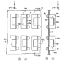
Fig. 3 is the schematic perspective view of a part that wherein forms the housing 50 of heat radiating fin 53.Fig. 4 A is the floor map of a part of the base plate 51 of housing 50, and Fig. 4 B is the cross sectional representation that the arrow IVB direction along Fig. 4 A obtains, and Fig. 4 C is the cross sectional representation that the arrow IVC direction along Fig. 4 A obtains.
Shown in Fig. 3 and Fig. 4 A-4C, a plurality of heat radiating fins 53 are formed in the housing 50 by the part that bending constitutes the base plate 51 of housing 50.Each heat radiating fin 53 comprises the first fin part 53A and the second fin part 53B.In the present embodiment, the first fin part 53A that constitutes each heat radiating fin 53 arranges and has along the Y direction width of about 40mm along Y direction among the figure.Each heat radiating fin 53 is arranged at each interval.In more detail, the first fin part 53A and the adjacent first fin part 53A are along directions X being spaced with about 28mm.In addition, the first fin part 53A and the adjacent first fin part 53A are along Y direction being spaced with about 20mm.
The first fin part 53A forms by the part along the direction of leaving LCD 10 (in other words being along the direction of leaving about 40) bending base plate 51.The first fin part 53A is basically perpendicular to base plate 51 and extends.It should be noted that the opening 54A that corresponds respectively to the first fin part 53A is formed in the base plate 51.Though in the present embodiment, the width of the first fin part 53A is set to about 15mm on the Z direction, the invention is not restricted to this.
The second fin part 53B forms by the part along the direction of leaving LCD 10 (in other words being along deviating from the direction of light source 40) the bending first fin part 53A.The second fin part 53B is basically parallel to base plate 51 and extends.In the present embodiment, the second fin part 53B forms by the middle body that bends the first fin part 53A.The second fin part 53B by bend with along among the figure+directions X extends.Note separately being formed in the base plate 51 corresponding to the opening 54B of the second fin part 53B.Although in the present embodiment, the second fin part 53B is configured to about 20mm and 10mm respectively along the width of Y direction and directions X, and the present invention is not limited to this.
Each light source 40 is set at the intersection of the first fin part 53A and base plate 51.More particularly, shown in Fig. 4 A-4C, two light sources 40 are set in each heat radiating fin 53, and each light source 40 is set on the position corresponding with the shank of the first fin part 53A and the intersection between the base plate 51.Because each light source 40 is set at the corresponding position of shank with the first fin part 53A, therefore the heat that is produced by light source 40 is passed to heat radiating fin 53 effectively.
According to said structure, heat radiating fin 53 forms one with the base plate 51 that constitutes housing 50.Therefore there is no need heat radiating fin 53 is fixed in base plate 51 as individual components.Because the second fin part 53B is by forming along the direction bending that deviates from as the light source 40 of giving birth to thermal source, therefore the second fin part 53B is set at low temperature side, thereby realizes the raising of cooling effectiveness.In addition, be formed among the first fin part 53A with the second fin part 53B corresponding opening 54B.Because heat radiating fin 53 is provided with separating each other and above-mentioned opening 54B is formed among the first fin part 53A, in each heat radiating fin 53, air duct is fixed to the direction (the Y direction among the figure) that is parallel to the first fin part 53A and perpendicular to the direction (directions X among the figure) of the first fin part 53A, so the heat of heat radiating fin 53 is discharged effectively.Therefore can realize good thermal diffusivity with low cost.
Liquid crystal display assembly 100 and planar light source device 60 are described above.To provide the summary of heat radiating fin 53 being revised example now.
To describe first in conjunction with Fig. 5 A-5C and revise example.Fig. 5 A is the floor map according to the part of the base plate 51 of the housing 50 of the first correction example, and Fig. 5 B is the cross sectional representation along the arrow VB direction acquisition of Fig. 5 A, and Fig. 5 C is the cross sectional representation along the arrow VC direction acquisition of Fig. 5 A.Other figure that revises example also is like this to aftermentioned.First revise the example place different with the structure shown in Fig. 4 A-4B be the second fin part 53B bent with along among the figure-the directions X extension.
Revising example below with reference to Fig. 6 A-6C to second describes.According to the second correction example, a heat radiating fin 53 is set corresponding to each light source 40.The second fin part 53B forms by the part (Y direction side) of the side of the bending first fin part 53A.
Revising example below in conjunction with Fig. 7 A-7C to the 3rd describes.The 3rd difference of revising structure shown in example and Fig. 6 A-6B is to be formed with in each heat radiating fin 53 a plurality of second fin part 53B.Specifically, the first fin part 53A is T shape substantially, and each second fin part 53B is formed along the shank symmetry of the part of first fin between them.Revise example according to the 3rd, be designed to the distance of revising example less than second from the distance in the path of light source 40 to second fin part 53B (heat that produced by light source 40 of more specifically saying so is passed to the distance in the path of the second fin part 53B by the first fin part 53A).Therefore, can be more efficiently with heat transferred to the second fin part 53B that produces by light source 40.
Revising example below in conjunction with Fig. 8 A-8C to the 4th is illustrated.According to the 4th embodiment, three light sources 40 are set corresponding to each heat radiating fin 53.In the embodiment shown in fig. 4, corresponding two light sources 40 are provided with one second fin part 53B.On the other hand, revise in the example at the 4th shown in Fig. 8 A-8C, corresponding three light sources 40 are provided with two second fin part 53B.In addition, the surface area of the first fin part 53B becomes greater than the area in embodiment illustrated in fig. 4.Therefore revise example according to the 4th, compare embodiment illustrated in fig. 4ly, the surface area of the heat radiating fin 53 corresponding with each light source 40 is bigger, realizes the further raising of cooling effectiveness thus.
Revising example below in conjunction with Fig. 9 A-9C to the 5th describes.The 5th revises the expansion that example is the 4th correction example.Revise in the example the 5th, form each heat radiating fin 53 along the Y direction continuously.Because the same cause that top reference the 4th embodiment describes, the surface area of the heat radiating fin 53 corresponding with each light source 40 becomes big, realizes the raising of cooling effectiveness thus.
Although by embodiment the present invention has been carried out description as above, yet the present invention is not limited to these embodiment.The configuration and the structure of the liquid crystal display assembly of Miao Shuing, planar light source device, LCD, light source etc. only are exemplary in the aforementioned embodiment, and the change that can suit.
Although in all embodiment, the first fin part 53A that constitutes each heat radiating fin 53 is along the setting of Y direction, yet the present invention is not limited to this.In addition, will all heat radiating fins 53 (more specifically, constituting the first fin part 53A of heat radiating fin 53) along same direction setting.For example, can heat radiating fin 53 be set interlace mode.The arrangement of light source 40 also is like this.
In all embodiment, each light source is made of light emitting diode (LED).Usually, between light emitting diode, there is the to a certain degree variation of luminescence efficiency.In addition, the luminescence efficiency of light emitting diode raises along with temperature usually and reduces.In addition, owing to be difficult to whole planar light source device is remained under the temperature of strict homogeneous, for the requirement in the design, there is variation to a certain degree in Temperature Distribution.Therefore, by based on luminescence efficiency light emitting diode (LED) being divided into groups in advance, the light emitting diode (LED) of high-luminous-efficiency is arranged on for designing requirement is in the zone of planar light source device of high-temperature region, and the light emitting diode (LED) that will hang down luminescence efficiency is arranged on for designing requirement and is in the raising of the homogeneity of the brightness of planar light source device in advance in the zone of low-temperature space planar light source device.
Claims (6)
1. liquid crystal display assembly comprises:
(a) LCD; And
(b) planar light source device illuminates described LCD from the back side,
Wherein said planar light source device comprises:
(A) comprise the housing of base plate;
(B) be arranged on the described base plate and illuminate the light source of described LCD; And
(C) a plurality of heat radiating fins that are intervally installed;
Wherein each heat radiating fin comprises:
(C-1) the first fin part forms by a part that bends described base plate along the direction that deviates from described LCD, and described first fin partly is basically perpendicular to described base plate and extends; And
(C-2) the second fin part, form by a part that bends described first fin part along the direction that deviates from described LCD, formed and the described corresponding opening of the second fin part (54B) in described first fin part simultaneously, described second fin partly is basically parallel to described base plate and extends.
2. liquid crystal display assembly as claimed in claim 1 is characterized in that a plurality of light sources are intervally installed, and each light source is set at the intersection between described first fin part and the described base plate.
3. liquid crystal display assembly as claimed in claim 1, it is characterized in that, the lid that surrounds described a plurality of heat radiating fins is configured to towards described base plate, is formed with air vent and air-blast device opening in described lid, and is provided with air-blast device in described air-blast device opening.
4. a planar light source device illuminates LCD from the back side, comprising:
(A) comprise the housing of base plate;
(B) be arranged on the described base plate and illuminate the light source of described LCD; And
(C) a plurality of heat radiating fins that are provided with at each interval;
Wherein each heat radiating fin comprises:
(C-1) the first fin part forms by a part that bends described base plate along the direction that deviates from described LCD, and described first fin partly is basically perpendicular to described base plate and extends; And
(C-2) the second fin part, form by a part that bends described first fin part along the direction that deviates from described LCD, formed and the described corresponding opening of the second fin part (54B) in described first fin part simultaneously, described second fin partly is basically parallel to described base plate and extends.
5. planar light source device as claimed in claim 4 is characterized in that a plurality of light sources are provided with at each interval, and each light source is set at the intersection between described first fin part and the described base plate.
6. planar light source device as claimed in claim 4 is characterized in that, the lid that surrounds described a plurality of heat radiating fins is configured to towards described base plate, is formed with air vent and air-blast device opening in described lid, and is provided with air-blast device in described air-blast device opening.
Applications Claiming Priority (2)
| Application Number | Priority Date | Filing Date | Title |
|---|---|---|---|
| JP2006155034A JP4952070B2 (en) | 2006-06-02 | 2006-06-02 | Planar light source device and liquid crystal display device assembly |
| JP2006155034 | 2006-06-02 |
Publications (2)
| Publication Number | Publication Date |
|---|---|
| CN101082708A CN101082708A (en) | 2007-12-05 |
| CN100541272C true CN100541272C (en) | 2009-09-16 |
Family
ID=38353250
Family Applications (1)
| Application Number | Title | Priority Date | Filing Date |
|---|---|---|---|
| CNB2007101098789A Expired - Fee Related CN100541272C (en) | 2006-06-02 | 2007-06-01 | Planar light source device and liquid crystal display assembly |
Country Status (7)
| Country | Link |
|---|---|
| US (1) | US7438450B2 (en) |
| EP (1) | EP1862844B1 (en) |
| JP (1) | JP4952070B2 (en) |
| KR (1) | KR101373264B1 (en) |
| CN (1) | CN100541272C (en) |
| DE (1) | DE602007001637D1 (en) |
| TW (1) | TWI356245B (en) |
Cited By (1)
| Publication number | Priority date | Publication date | Assignee | Title |
|---|---|---|---|---|
| CN102278668A (en) * | 2010-06-11 | 2011-12-14 | Lg伊诺特有限公司 | Backlight unit and display device including the same |
Families Citing this family (25)
| Publication number | Priority date | Publication date | Assignee | Title |
|---|---|---|---|---|
| JP2008020532A (en) * | 2006-07-11 | 2008-01-31 | Fujifilm Corp | Optical functional sheet and display device |
| WO2008090642A1 (en) * | 2007-01-24 | 2008-07-31 | Sharp Kabushiki Kaisha | Backlight structure |
| US8049689B2 (en) * | 2007-05-31 | 2011-11-01 | Motorola Mobility, Inc. | Devices and methods for synchronized illumination |
| JP2008305713A (en) * | 2007-06-08 | 2008-12-18 | Fujifilm Corp | Surface illumination device |
| EP2182502B1 (en) * | 2007-08-20 | 2014-11-12 | Mitsubishi Electric Corporation | Display device |
| US7661865B2 (en) * | 2007-10-17 | 2010-02-16 | Nec Lcd Technologies, Ltd. | Liquid crystal display backlight and liquid crystal display device |
| KR101407622B1 (en) * | 2007-11-09 | 2014-06-13 | 삼성디스플레이 주식회사 | Display apparatus |
| TWI367717B (en) * | 2007-12-13 | 2012-07-01 | Young Lighting Technology Corp | Backlight module |
| JP5107737B2 (en) * | 2008-01-29 | 2012-12-26 | 株式会社ジャパンディスプレイイースト | Liquid crystal display |
| US20110134148A1 (en) * | 2008-03-11 | 2011-06-09 | William Robert Cridland | Systems And Methods Of Processing Touchpad Input |
| JPWO2010070917A1 (en) * | 2008-12-17 | 2012-05-24 | カラーリンク・ジャパン 株式会社 | Image display device |
| KR20100087950A (en) | 2009-01-29 | 2010-08-06 | 삼성전자주식회사 | Backlight assembly and liquid crystal display using the same |
| US20100220487A1 (en) * | 2009-02-27 | 2010-09-02 | Hong Kong Applied Science And Technology Research Institute Co. Ltd. | Lighting assembly and heat exchange apparatus for uniform heat dissipation |
| US8152337B2 (en) * | 2009-05-01 | 2012-04-10 | Billboard Video, Inc. | Electronic display panel |
| US20100302769A1 (en) * | 2009-05-28 | 2010-12-02 | Alex Horng | Lamp |
| US20120236499A1 (en) * | 2009-12-03 | 2012-09-20 | Panasonic Corporation | Radiation unit of electronic device and electronic device using same |
| US9395057B2 (en) * | 2011-02-07 | 2016-07-19 | Cree, Inc. | Lighting device with flexibly coupled heatsinks |
| WO2012157548A1 (en) * | 2011-05-18 | 2012-11-22 | シャープ株式会社 | Illumination device and display device |
| JP2013218125A (en) * | 2012-04-10 | 2013-10-24 | Japan Display Inc | Liquid-crystal display |
| JP2014053143A (en) * | 2012-09-06 | 2014-03-20 | Aps Japan Co Ltd | Luminaire |
| JP5960044B2 (en) * | 2012-12-26 | 2016-08-02 | 船井電機株式会社 | Display device |
| CN104832836A (en) * | 2015-04-29 | 2015-08-12 | 武汉华星光电技术有限公司 | Back plate, backlight module and display device |
| TWI623254B (en) * | 2016-03-31 | 2018-05-01 | 揚昇照明股份有限公司 | Electronic device |
| AU2018355133A1 (en) * | 2017-10-19 | 2020-06-04 | Alpine Media Technology Llc | Method, energy unit, housing, and device for delivering information content to mobile units |
| KR101940987B1 (en) * | 2018-08-21 | 2019-01-23 | 네오마루 주식회사 | Printed circuit board with heatsink for led lighting apparatus |
Family Cites Families (13)
| Publication number | Priority date | Publication date | Assignee | Title |
|---|---|---|---|---|
| GB1150741A (en) | 1965-04-26 | 1969-04-30 | Eric Imre Bardos | Heat Sinks and Manufacture thereof |
| JPH04125615A (en) * | 1990-09-18 | 1992-04-27 | Pioneer Electron Corp | Cooling system for liquid crystal display device |
| JPH04317024A (en) * | 1991-04-16 | 1992-11-09 | Sanyo Electric Co Ltd | Cooling device for liquid crystal panel |
| US5375655A (en) * | 1993-03-31 | 1994-12-27 | Lee; Yong N. | Heat sink apparatus |
| JP2001337611A (en) * | 2000-03-22 | 2001-12-07 | Furukawa Electric Co Ltd:The | Frame of display device |
| US6825828B2 (en) * | 2001-02-23 | 2004-11-30 | General Digital Corporation | Backlit LCD monitor |
| US6650215B1 (en) * | 2002-06-17 | 2003-11-18 | The Bergquist Company | Finned heat sinks |
| TW542883B (en) * | 2002-08-16 | 2003-07-21 | Au Optronics Corp | Backlight unit for flat panel liquid crystal display |
| JP4622327B2 (en) * | 2004-06-14 | 2011-02-02 | ソニー株式会社 | Liquid crystal display device and backlight device |
| JP4385891B2 (en) | 2004-08-18 | 2009-12-16 | ソニー株式会社 | Display device |
| TWI297796B (en) * | 2004-11-09 | 2008-06-11 | Au Optronics Corp | Flat display and backlight module thereof |
| TWI263836B (en) * | 2004-11-12 | 2006-10-11 | Coretronic Corp | Heat dissipation method of display backlight unit and the structure thereof |
| JP2007027056A (en) * | 2005-07-21 | 2007-02-01 | Sony Corp | Backlight unit and liquid crystal display device |
-
2006
- 2006-06-02 JP JP2006155034A patent/JP4952070B2/en not_active Expired - Fee Related
-
2007
- 2007-05-17 TW TW096117644A patent/TWI356245B/en not_active IP Right Cessation
- 2007-05-29 US US11/807,573 patent/US7438450B2/en active Active
- 2007-05-30 KR KR1020070052645A patent/KR101373264B1/en active IP Right Grant
- 2007-05-31 DE DE602007001637T patent/DE602007001637D1/en active Active
- 2007-05-31 EP EP07252223A patent/EP1862844B1/en active Active
- 2007-06-01 CN CNB2007101098789A patent/CN100541272C/en not_active Expired - Fee Related
Cited By (2)
| Publication number | Priority date | Publication date | Assignee | Title |
|---|---|---|---|---|
| CN102278668A (en) * | 2010-06-11 | 2011-12-14 | Lg伊诺特有限公司 | Backlight unit and display device including the same |
| CN102278668B (en) * | 2010-06-11 | 2014-04-16 | Lg伊诺特有限公司 | Backlight unit and display device including the same |
Also Published As
| Publication number | Publication date |
|---|---|
| KR101373264B1 (en) | 2014-03-11 |
| US20070279930A1 (en) | 2007-12-06 |
| JP4952070B2 (en) | 2012-06-13 |
| US7438450B2 (en) | 2008-10-21 |
| JP2007322905A (en) | 2007-12-13 |
| CN101082708A (en) | 2007-12-05 |
| TW200813564A (en) | 2008-03-16 |
| EP1862844B1 (en) | 2009-07-22 |
| EP1862844A1 (en) | 2007-12-05 |
| DE602007001637D1 (en) | 2009-09-03 |
| KR20070115709A (en) | 2007-12-06 |
| TWI356245B (en) | 2012-01-11 |
Similar Documents
| Publication | Publication Date | Title |
|---|---|---|
| CN100541272C (en) | Planar light source device and liquid crystal display assembly | |
| CN100381895C (en) | Display device | |
| CN100435005C (en) | Backlight unit and liquid crystal display employing the same | |
| KR102297410B1 (en) | Outdoor display apparatus | |
| CN103115284B (en) | Back light unit and the display device with this back light unit | |
| TWI479234B (en) | Display apparatus | |
| US20160291397A1 (en) | Display device | |
| JP2006178451A (en) | Backlight system and liquid crystal display device employing same | |
| CN102518980A (en) | Backlight unit and display apparatus having the same | |
| CN201606739U (en) | LED backlight module | |
| CN102713428A (en) | Lighting device, display device, and television reception device | |
| EP3043110A1 (en) | Light bar and display device | |
| RU2500951C2 (en) | Lighting unit, display device and tv receiver | |
| JP2008311026A (en) | Surface light source device | |
| CN104487762B (en) | Planar light source device and liquid crystal indicator | |
| KR100780187B1 (en) | LCD BACKLIGHT UNIT USING LEDs | |
| KR101108426B1 (en) | Backlight unit of liquid crystal display device | |
| JP2008140653A (en) | Surface light source device and liquid crystal display device assembly | |
| JP2010129359A (en) | Backlight unit and liquid crystal display device | |
| KR20070108712A (en) | Back light unit | |
| CN104197246B (en) | Side-entering type backlight module and liquid crystal indicator | |
| WO2012026162A1 (en) | Lighting apparatus, display apparatus, and television receiver apparatus | |
| JP2007184493A (en) | Light source device and display device | |
| KR100688979B1 (en) | Backlight unit | |
| JP6452073B2 (en) | LIGHT EMITTING DEVICE AND APPARATUS HAVING LIGHT EMITTING DEVICE |
Legal Events
| Date | Code | Title | Description |
|---|---|---|---|
| C06 | Publication | ||
| PB01 | Publication | ||
| C10 | Entry into substantive examination | ||
| SE01 | Entry into force of request for substantive examination | ||
| C14 | Grant of patent or utility model | ||
| GR01 | Patent grant | ||
| CF01 | Termination of patent right due to non-payment of annual fee | ||
| CF01 | Termination of patent right due to non-payment of annual fee |
Granted publication date: 20090916 Termination date: 20200601 |