CN100521135C - Polarization analyzing method - Google Patents
Polarization analyzing method Download PDFInfo
- Publication number
- CN100521135C CN100521135C CNB038036142A CN03803614A CN100521135C CN 100521135 C CN100521135 C CN 100521135C CN B038036142 A CNB038036142 A CN B038036142A CN 03803614 A CN03803614 A CN 03803614A CN 100521135 C CN100521135 C CN 100521135C
- Authority
- CN
- China
- Prior art keywords
- layer
- photopermeability
- polarized light
- light component
- analysis method
- Prior art date
- Legal status (The legal status is an assumption and is not a legal conclusion. Google has not performed a legal analysis and makes no representation as to the accuracy of the status listed.)
- Expired - Fee Related
Links
Images


Classifications
-
- G—PHYSICS
- G01—MEASURING; TESTING
- G01B—MEASURING LENGTH, THICKNESS OR SIMILAR LINEAR DIMENSIONS; MEASURING ANGLES; MEASURING AREAS; MEASURING IRREGULARITIES OF SURFACES OR CONTOURS
- G01B11/00—Measuring arrangements characterised by the use of optical techniques
- G01B11/02—Measuring arrangements characterised by the use of optical techniques for measuring length, width or thickness
- G01B11/06—Measuring arrangements characterised by the use of optical techniques for measuring length, width or thickness for measuring thickness ; e.g. of sheet material
- G01B11/0616—Measuring arrangements characterised by the use of optical techniques for measuring length, width or thickness for measuring thickness ; e.g. of sheet material of coating
- G01B11/0641—Measuring arrangements characterised by the use of optical techniques for measuring length, width or thickness for measuring thickness ; e.g. of sheet material of coating with measurement of polarization
-
- G—PHYSICS
- G01—MEASURING; TESTING
- G01N—INVESTIGATING OR ANALYSING MATERIALS BY DETERMINING THEIR CHEMICAL OR PHYSICAL PROPERTIES
- G01N21/00—Investigating or analysing materials by the use of optical means, i.e. using sub-millimetre waves, infrared, visible or ultraviolet light
- G01N21/17—Systems in which incident light is modified in accordance with the properties of the material investigated
- G01N21/21—Polarisation-affecting properties
- G01N21/211—Ellipsometry
Landscapes
- Physics & Mathematics (AREA)
- General Physics & Mathematics (AREA)
- General Health & Medical Sciences (AREA)
- Chemical & Material Sciences (AREA)
- Analytical Chemistry (AREA)
- Biochemistry (AREA)
- Life Sciences & Earth Sciences (AREA)
- Health & Medical Sciences (AREA)
- Immunology (AREA)
- Pathology (AREA)
- Length Measuring Devices By Optical Means (AREA)
- Investigating Or Analysing Materials By Optical Means (AREA)
- Testing Or Measuring Of Semiconductors Or The Like (AREA)
Abstract
Under an oxide film (301), a multilayer interconnection comprising a layer B composed of a metal interconnection (302) and an interlayer insulating film (303) and a layer D composed of a metal interconnection (304) extending in a direction perpendicular to the metal interconnection (302) and an interlayer insulating film (305) is formed. Assuming that the s-polarized light of the incident light is reflected from the interface of the layer B, and the p-polarized light is reflected from the interface of the layer D, the amplitude reflectances Rs and Rp are calculated, and tan [Psi] of a function of the amplitude ratio [Psi] between the s- and p-polarized components and cos DELTA of a function of the phase difference DELTA between them are calculated, thereby creating reference data. The thickness (tA) of the oxide film (301) is determined on the basis of the reference data. Thus, the thickness and cross section shape of the film formed on the multilayer interconnection are measured in a nondestructive manner with high throughput.
Description
Technical field
The present invention relates to a kind of polarization analysis method, the polarization analysis method that is fit in particularly a kind of film thickness measuring of the manufacturing process at semiconductor device, the measurement of etching shape prismatic shapes.
Background technology
All the time, for example in the thickness of the manufacturing process of semiconductor device is checked operation etc., utilize the blooming that uses ellipsometer to measure.
Fig. 2 is the figure that the roughly situation that the blooming of this ellipsometer measures is used in expression.As scheme above-mentioned, in the blooming that uses ellipsometer is measured, will be from the light of light source 101, by the polarization element 102 of adjusting polarization state, each optical element of adjusting the compensating plate 103 of phase place, form the incident light of elliptical polarization state thus, shine on the sample 107.
Then, on catoptrical light path from sample 107, be provided for adjusting polarization state testing light element 104, be used to select optical splitter 105, the detector 106 of the light of provision wavelengths, for catoptrical each wavelength measurement polarization state, obtain spectrum.
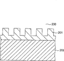
For example, as shown in Figure 3, under situation about measuring at the thickness of the oxide-film (gate oxidation films etc.) 201 of film forming on the Si substrate 202, as described above, from air (the refractive index=N0) 200 with the incident light of the elliptical polarization state of angle θ 0 irradiation, (refractive index=N1) 201 surface reflections, simultaneously, its major part incides in the oxide-film 201 by oxide-film.Afterwards, incide the light of the incident in the oxide-film 201, (refractive index=N2) reflection turns back in oxide-film 201 air 200, with the reverberation polarization interference on oxide-film 201 surfaces by Si substrate 202 interfaces (real estate).
For above-mentioned such light, calculate each p polarized light component and s polarized light component, calculate thickness by each phase difference and amplitude ratio ψ.
The catoptrical p polarized light component (r that the Si substrate is 202
1p) and s polarized light component (r
1s), calculate by following formula respectively.
r1p=(n2cosθ1—n1cosθ2)/(n2cosθ1+n1cosθ2)
r1s=(n1cosθ1—n2cosθ2)/(n1cosθ1+n2cosθ2)
In addition, the p polarized light component (Rp) of the light of detection and s polarized light component (Rs) can calculate polarization state by following formula according to the catoptrical p polarized light component (r0p) and the s polarized light component (r0s) of 201 of above-mentioned r1p, r1s and oxide-films.
Rp=(r0p+r1pexp(-2iδ))/(1+r0p·r1pexp(—2iδ))
Rs=(r0s+r1sexp(—2iδ))/(1+r0s·r1sexp(—2iδ))
Wherein, (δ=2 π n
1Tcos θ
1/ λ)
Finally, use Rp/Rs=tan (ψ) exp (-i Δ), each wavelength is calculated cos Δ and tan ψ, obtain wavelength thus and rely on spectrum.Then, as parameter, relatively Shi Ce spectrum and theoretical spectrum can calculate film thickness value t thus with the film thickness value t of oxide-film 201.
In addition, as shown in Figure 4, the oxide-film 201 that on Si substrate 202, forms, under situation with grid system (grating structure), also can utilize ellipsometer to carry out the measurement of the cross sectional shape of this grid system, in this case, as shown in Figure 5, pattern part is divided into the L five equilibrium, the grid part is obtained shape as the laminated film of L layer.In this method, there is the mixed layer of the dielectric constant of air and grid system, utilize the pattern that n diffraction light takes place at each interface to calculate cross sectional shape.In this case, grid pattern shown in Figure 5 is assumed to be unlimited repeat region.Grid system is divided into the L layer, recently settles accounts dielectric constant based on the air of each layer and the volume of grid part.During with the angle incident light of the lamination structure that is in this L layer, be structured in the such model of n diffraction light that reflection takes place and see through in the interface of each layer, calculate the amplitude reflectance of s polarized light component, p polarized light component respectively.Finally can obtain cross sectional shape according to the wavelength dependency of cos Δ and tan ψ.
In the above-mentioned film thickness measuring method, in the method for measurement of any cross sectional shape, real estate (lower floor's reflecting surface) is made of the big material (the low photopermeability material that photopermeability is low) of absorption coefficient of light k such as Si, Al, Cu, can be applicable to the situation of the non-permeability that thickness is thicker, smooth.
But, in above-mentioned film thickness measuring method and cross sectional shape method of measurement, have in lower floor under the situation of sample of multi-layer circuit structure as the oxide-film of measuring object, have and can not carry out film thickness measuring and cross sectional shape is measured such problem.
Promptly, for example, under sample situation as shown in Figure 6, shown in Fig. 6 (a), lower floor at a layer that constitutes by oxide-film 301 as the object of measuring thickness, the b layer that formation is made of metal line 302 and interlayer dielectric 303, the c layer that is made of metal line 304 and interlayer dielectric 305 shown in this figure (b), (c), have and make metal line 304 quadratures of the metal line 302 of b layer and c layer and the multi-layer circuit structure that forms.In such multi-layer circuit structure, oxide-film 301 and interlayer dielectric 303,305 are made of the high high photopermeability material of photopermeabilities such as silicon dioxide, and metal line 302,304 is made of low low photopermeability materials of photopermeability such as Cu, Al, W.And in Fig. 6 (a), 306,307 are made of SiN film or SiC film etc., be utilized in CMP (chemico-mechanical polishing) operation stop (stopper) layer.
In addition, under the situation of sample shown in Figure 7, in addition, oxide-film 301 has grid system.
Under the situation of sample with above-mentioned such multi-layer circuit structure, because the structure of the reflecting surface of lower floor is complicated, so when theory of computation spectrum, suppose to come theory of computation spectrum by the surface of a layer and the boundary reflection of a layer and b layer, both made hypothesis be reflected theory of computation spectrum, and can not carry out film thickness measuring and cross sectional shape and measure by the surface of a layer and the interface of b layer and c layer.
For this reason, all the time, under the situation of film thickness measuring of the film that carries out forming on the multi-layer circuit structure etc., in manufacturing process, drop into the sample wafer different, go up the film that becomes measuring object, carry out film thickness measuring by optical means at sample wafer (naked Si) with the goods wafer.
In addition, both made under the situation of measuring the etching shape, also will drop into sample wafer, film forming, coating against corrosion, exposure, etching work procedure, observed the cross section, carried out the shape management by SEM.
For this reason, under any circumstance, having many more its manufacturing costs of sample wafer number increases such problem more.
In addition, the supervision pattern of film thickness measuring or etching shape measure can be set in chip also, utilize existing method to measure this position.But, highly integrated along with IC, it is difficult in chip the supervision pattern with a certain size being set.In addition, because the pattern that is provided with as hypothesis is bigger, so in the operation of CMP is handled, the surface that causes metal line 302 as shown in Figure 8 is cut the concavity of bowl type, measuring as reflecting surface under the situation of thickness etc., have certainty of measurement and worsen such problem with the interface of metal line 302.
Therefore, for thickness and the cross sectional shape of measuring, manage the film that on multilayer wiring, forms, seek to measure the exploitation of method of the optional position of goods wafer with non-destruction, high production rate.
Summary of the invention
The objective of the invention is to, a kind of polarization analysis method is provided, its can non-destruction and the high production rate ground film thickness measuring and the cross sectional shape that carry out the film that on multilayer wiring, forms measure.
The invention provides a kind of polarization analysis method, the measured object of film that has measuring object on to the surface is during with the incident light of the elliptical polarization state of regulation incidence angle irradiation provision wavelengths, by Theoretical Calculation obtain from the catoptrical p polarized light component of above-mentioned measured object reflection and s polarized light component based on the value of phase difference (Δ) with based on the value of amplitude ratio (Ψ), obtain reference data, simultaneously, by measurement obtain actual catoptrical p polarized light component that reflects when above-mentioned measured object is shone above-mentioned incident light and s polarized light component based on the value of phase difference (Δ) with based on the value of amplitude ratio (Ψ), by comparing with the said reference data, carry out the analysis of above-mentioned film, it is characterized in that, when obtaining the said reference data, make that the reflecting surface of above-mentioned p polarized light component is different with the reflecting surface of above-mentioned s polarized light component, carry out above-mentioned theory and calculate.
In addition, the present invention is characterised in that above-mentioned comparison is carried out based on the wavelength more than at least 2.
In addition, the present invention is characterised in that above-mentioned comparison is carried out based on the incidence angle more than at least 2.
In addition, the invention is characterized in, is the cos Δ based on the value of above-mentioned phase difference (Δ), is tan Ψ based on the value of above-mentioned amplitude ratio (Ψ).
In addition, the invention is characterized in that above-mentioned measured object has: the ground floor that forms in the superiors, constitute by the high high photopermeability material of photopermeability; The second layer that under above-mentioned ground floor, is provided with, constituted by high high photopermeability material of photopermeability and the low low photopermeability material of photopermeability; Under the second layer, be provided with, constituted by the high high photopermeability material of photopermeability the 3rd layer; The substrate that under above-mentioned the 3rd layer, is provided with, constituted by the low low photopermeability material of photopermeability.
In addition, the invention is characterized in, in the above-mentioned second layer, above-mentioned high photopermeability material and above-mentioned low photopermeability material have linearity Wiring structure, the polarization plane of above-mentioned p polarized light component and the above-mentioned linearity cloth line parallel in the mutual configuration of layer plane direction.
In addition, the invention is characterized in, between aforesaid substrate and above-mentioned the 3rd layer, the low photopermeability material that high photopermeability material that photopermeability is high and photopermeability are low, have the 4th layer, it has the linearity Wiring structure in the mutual configuration of layer plane direction at least from the teeth outwards, and the direction of above-mentioned the 4th layer linearity wiring is the direction with the linearity wiring direction quadrature of the above-mentioned second layer.
In addition, the invention is characterized in that above-mentioned s polarized light component reflects on the above-mentioned second layer, above-mentioned p polarized light component sees through the above-mentioned second layer, reflection on above-mentioned the 4th layer.
In addition, the invention is characterized in that the above-mentioned second layer during above-mentioned theory is calculated is different to the refractive index of above-mentioned p polarized light component with refractive index to above-mentioned s polarized light component.
In addition, the invention is characterized in that the low photopermeability material that above-mentioned photopermeability is low is the metal line material, the high photopermeability material that above-mentioned photopermeability is high is an insulating material.
In addition, the invention is characterized in, measure the film of above-mentioned measuring object thickness, refractive index, cross sectional shape at least any one.
Description of drawings
Fig. 1 is the figure that is used to illustrate an execution mode of method of measurement of the present invention.
Fig. 2 is the figure that roughly constitutes of the employed ellipsometer of expression the inventive method.
Fig. 3 is the figure that roughly constitutes in the expression substrate cross section that is used to illustrate existing film thickness measuring method.
Fig. 4 is the figure that roughly constitutes in the expression substrate cross section that is used to illustrate existing cross sectional shape method of measurement.
Fig. 5 is the figure that roughly constitutes in the expression substrate cross section that is used to illustrate existing cross sectional shape method of measurement.
Fig. 6 is the figure that roughly constitutes in the substrate cross section of the expression problem points that is used to illustrate prior art.
Fig. 7 is the figure that roughly constitutes in the substrate cross section of the expression problem points that is used to illustrate prior art.
Fig. 8 is the figure that roughly constitutes in the substrate cross section of the expression problem points that is used to illustrate prior art.
Embodiment
Below, about execution mode details of the present invention is described with reference to accompanying drawing.
Fig. 1 has represented to measure the example of situation of thickness (tA) of the oxide-film 301 of above-mentioned sample with multi-layer circuit structure shown in Figure 6, so in the figure, for the purpose of simplifying the description, about barrier layer shown in Figure 6 306,307, has omitted diagram.In addition, in the figure, (a) movement of the s polarized light component in the light of expression irradiation, (b) movement of expression p polarized light component.And, measure the formation of employed ellipsometer, as shown in Figure 2 above-mentioned, constitute by light source 101, polarization element 102, compensating plate 103, testing light element 104, optical splitter 105, detector 106 etc.
Shown in Fig. 1 (a), shining from refractive index is the air 300 of N0 by refractive index is the s polarized light component of the incident light of the A layer that constitutes of the oxide-film 301 of NA, and from A laminar surface reflection (r0s), remainder incides the A layer to its part with angle of reflection θ 0.
Then, the s polarized light component that incides in the A layer passes through the A layer, the interface of the B layer that arrival is made of metal line 302 and interlayer dielectric 303, but the s polarized light component has amplitude in the direction vertical with the wiring direction (length direction of wiring) of metal line 302, so, can not be by in the formation zone of the interlayer dielectric 303 of 302 formation of metal line of B layer, with the interface of B layer with angle of reflection θ 1 reflection.This catoptrical amplitude reflectance r1s is by following expression:
r1s=(NAcosθ1—NBscosθ2)/(NAcosθ1+NBscosθ2)
And NBs is the refractive index to the s polarized light component of B layer.
This reverberation (r1s) is by the B layer, and with reverberation (r0s) interference by the reflection of A laminar surface, the amplitude reflectance Rs of its interference light is:
Rs=(r0s+r1s?exp(—2iδ))/(1+r0s·r1s?exp(—2iδ))
Wherein,
δ=2πNAtAcosθ1/λ
r0s=(N0cosθ0—NAcosθ1)/(N0cosθ0+NAcosθ1)
On the other hand, the movement of p polarized light component in Fig. 1 (b) expression irradiates light.Shining from refractive index is the air 300 of N0 by refractive index is the p polarized light component of the incident light of the A layer that constitutes of the oxide-film 301 of NA, and from A laminar surface reflection (r0p), remainder incides in the A layer its part with angle of reflection θ 0.
Then, incide the p polarized light component in the A layer, by the A layer, arrive interface with the B layer that constitutes by metal line 302 and interlayer dielectric 303, but because the p polarized light component has amplitude in the direction parallel with the wiring direction (length direction of wiring) of metal line 302, so can form the zone by interlayer dielectric 303 in 302 formation of B layer metal line.Then, the p polarized light component that should pass through is the C layer by only being made of interlayer dielectric 303 also, arrives the interface with the D layer that is made of metal line 304 and interlayer dielectric 305.And, and, as shown in the drawing, with the interface of B layer, with the interface of C layer, a part of p polarized light component is with angle of reflection θ 1, θ 2 reflections.
The amplitude direction of the metal line 304 relative p polarized light components of D layer is vertical, so the p polarized light component can not pass through to form the zone at the interlayer dielectric 305 of 304 formation of metal line of D layer, the p polarized light component at the interface of arrival and D layer is here with angle of reflection θ 3 reflections.This catoptrical amplitude reflectance r3p is by following formulate:
r3p=(NDcosθ3—NCcosθ4)/(NDcosθ3+NCcosθ4)
The B layer of relative s polarized light component and the D layer of relative p polarized light component, act as real estate (the non-face that sees through) in fact, so at the refractive index NBs of the relative B layer of s polarized light component with relatively between the refractive index ND of the D layer of p polarized light component, ND=NBs sets up.But, be limited to the live width of metal line of B layer and C layer and situation about equating at interval.
By with the reverberation (r3p) of the boundary reflection of D layer by the C layer, and interfere by the reverberation (r2p) that reflects with the interface of C layer, the amplitude reflectance R2p of this interference light is:
R2p=(r2p+r3p?exp(—2iδ))/(1+r2p·r3p?exp(—2iδ))
But,
δ=2πNC?tCcosθ3/λ
r2p=(NC?cosθ2—NBpcosθ3)/(NC?cosθ2+NBpcosθ3)
Here, as describing, in the calculating of s polarized light component, the refractive index of B layer is defined as NBs, but the B layer is to comprise the layer that changes the metals such as Cu, W, Al of refractive index because of thickness about the B layer.Under the situation of such layer, play at s polarized light component relatively under the situation of function of real estate (the non-face that sees through) with relative p polarized light component and conduct through under the situation of film performance function, refractive index difference, NBs ≠ NBp.
By under the situation of B layer, if consideration too, the amplitude reflectance R1p of B layer is at above-mentioned interference light (R2p):
R1p=(r1p+R2p?exp(—2iδ))/(1+r1p·R2p?exp(—2iδ))
But,
δ=2πNBp?tBcosθ2/λ
r1p=(NBpcosθ1—NAcosθ2)/(NBp?cosθ1+NA?cosθ2)
Finally, the amplitude reflectance Rp of A laminar surface is:
Rp=(r0p+R1p?exp(—2iδ))/(1+r0p·R1p?exp(—2iδ))
But,
δ=2πNA?tAcosθ1/λ
r0p=(NA?cosθ0—N0cosθ1)/(NA?cosθ0+N0cosθ1)
As mentioned above, at the reflecting surface that act as real estate (the non-face that sees through), according to being divided into amplitude reflectance Rs, the Rp that s polarized light component and p polarized light component calculate respectively, can calculate by following formula as the tan ψ and the cos Δ of the function of the amplitude ratio ψ of s polarized light component and p polarized light component and phase difference:
Rs/Rp=tanψ·exp(—iΔ)
More than be illustrated about random wave length, so,, can obtain the λ-tan ψ as reference data and the spectroscopic data of λ-cos Δ by calculating tan ψ and cos Δ for continuous a plurality of wavelength.
Then, distribution comes the spectroscopic data of the reference data that comparison obtains like this about the different thick tA of A tunic and the spectroscopic data of the actual measurement that actual measurement obtains about thickness and membranous parameter, the thickness that the statistic of this error of expression is minimum or maximum is as output valve, utilize this method, can measure the thickness of the oxide-film 301 (A layer) that on multilayer wiring, forms.
And under the situation of sample half-twist, also can be s polarized light component and p polarized light component reflection, see through opposite pattern.
In addition, as above-mentioned, the s polarized light component is reflected by each different face respectively with the p polarized light component, calculate the wavelength dependency of tan ψ and cos Δ, with the spectrum method relatively of actual measurement, as shown in Figure 7, also can be used in the etching shape measure prismatic shapes measurement of grid system.Calculate about the cross sectional shape that forms in the superiors, use such method, as shown in Figure 5, pattern part is divided into the n five equilibrium, the grid part is obtained shape as n lamination tunic.
In addition, in the above-described embodiment, the situation of the metal line 302,304 that on B layer and D layer formation is mutually orthogonal has been described, but for the D layer of lower floor, both having made there is not metal line 304, is made of non-faces that sees through such as real estates, and can be suitable for too.
In addition, also can access same effect by replacing wavelength to change incidence angle.For example, in Fig. 1, change incidence angle θ 0 and measure, obtain the incident angle dependency of cos Δ and tan ψ.Then, utilize a plurality of incidence angles to calculate, obtain the reference data of θ-cos Δ and θ-tan ψ based on above-mentioned formula.The spectroscopic data of benchmark data and actual measurement can be obtained the physical quantity about the thickness and the cross sectional shape of hope.
More than be illustrated, as according to the present invention, can non-destruction and the high production rate ground film thickness measuring and the cross sectional shape that carry out the film that on multilayer wiring, forms measure.
Utilizability on the industry
Polarization analyzing method of the present invention is in the semiconductor manufacturing of the manufacturing of carrying out semiconductor device Can use in the industry etc. Therefore, has utilizability on the industry.
Claims (11)
1. polarization analysis method, the measured object of film that has measuring object on to the surface is during with the incident light of the elliptical polarization state of regulation incidence angle irradiation provision wavelengths, by Theoretical Calculation obtain from the catoptrical p polarized light component of described measured object reflection and s polarized light component based on the value of phase difference with based on the value of amplitude ratio Ψ, obtain reference data, simultaneously
By measurement obtain actual catoptrical p polarized light component that reflects when described measured object is shone described incident light and s polarized light component based on the value of phase difference with based on the value of amplitude ratio Ψ, by comparing with described reference data, carry out the analysis of described film, it is characterized in that
When obtaining described reference data, making that the reflecting surface of described p polarized light component is different with the reflecting surface of described s polarized light component carries out described Theoretical Calculation.
2. polarization analysis method according to claim 1 is characterized in that,
Described comparison is carried out based on the wavelength more than at least 2.
3. polarization analysis method according to claim 1 is characterized in that,
Described comparison is carried out based on the incidence angle more than at least 2.
4. polarization analysis method according to claim 1 is characterized in that,
Value based on described phase difference is the cos Δ, is tan Ψ based on the value of described amplitude ratio Ψ.
5. polarization analysis method according to claim 1 is characterized in that,
Described measured object has:
The ground floor that forms in the superiors, constitute by the high high photopermeability material of photopermeability;
The second layer that under described ground floor, is provided with, constituted by high high photopermeability material of photopermeability and the low low photopermeability material of photopermeability;
Under the second layer, be provided with, constituted by the high high photopermeability material of photopermeability the 3rd layer;
The substrate that under described the 3rd layer, is provided with, constituted by the low low photopermeability material of photopermeability.
6. polarization analysis method according to claim 5 is characterized in that,
In the described second layer, described high photopermeability material and described low photopermeability material have the linearity Wiring structure in the mutual configuration of layer plane direction,
The polarization plane of described p polarized light component and described linearity cloth line parallel.
7. polarization analysis method according to claim 6 is characterized in that,
Between described substrate and described the 3rd layer, the low photopermeability material that high photopermeability material that photopermeability is high and photopermeability are low has the 4th layer that has at least from the teeth outwards at the linearity Wiring structure of the mutual configuration of layer plane direction,
The direction of described the 4th layer linearity wiring is the direction with the linearity wiring direction quadrature of the described second layer.
8. polarization analysis method according to claim 7 is characterized in that,
Described s polarized light component reflects on the described second layer, and described p polarized light component sees through the described second layer, reflection on described the 4th layer.
9. polarization analysis method according to claim 5 is characterized in that,
The described second layer in the described Theoretical Calculation is different to the refractive index of described p polarized light component with refractive index to described s polarized light component.
10. polarization analysis method according to claim 5 is characterized in that,
The low photopermeability material that described photopermeability is low is the metal line material, and the high photopermeability material that described photopermeability is high is an insulating material.
11. polarization analysis method according to claim 1 is characterized in that,
Measure the film of described measuring object thickness, refractive index, cross sectional shape at least any one.
Applications Claiming Priority (2)
| Application Number | Priority Date | Filing Date | Title |
|---|---|---|---|
| JP2002040506A JP3878027B2 (en) | 2002-02-18 | 2002-02-18 | Polarization analysis method and optical film thickness measuring apparatus |
| JP40506/2002 | 2002-02-18 |
Publications (2)
| Publication Number | Publication Date |
|---|---|
| CN1630940A CN1630940A (en) | 2005-06-22 |
| CN100521135C true CN100521135C (en) | 2009-07-29 |
Family
ID=27678309
Family Applications (1)
| Application Number | Title | Priority Date | Filing Date |
|---|---|---|---|
| CNB038036142A Expired - Fee Related CN100521135C (en) | 2002-02-18 | 2003-02-10 | Polarization analyzing method |
Country Status (5)
| Country | Link |
|---|---|
| US (1) | US6950186B2 (en) |
| JP (1) | JP3878027B2 (en) |
| CN (1) | CN100521135C (en) |
| AU (1) | AU2003207200A1 (en) |
| WO (1) | WO2003069667A1 (en) |
Families Citing this family (14)
| Publication number | Priority date | Publication date | Assignee | Title |
|---|---|---|---|---|
| DE10319843A1 (en) | 2003-05-03 | 2004-12-02 | Infineon Technologies Ag | Depth measurement system for determining depth of blind bores in semiconductor workpieces has IR source with beam splitter and polarizer directing beam into workpiece at 45 degree angle |
| TWI460418B (en) | 2005-11-29 | 2014-11-11 | Horiba Ltd | Manufacturing method and manufacturing equipment of organic el element |
| JP4317558B2 (en) * | 2006-08-23 | 2009-08-19 | 株式会社堀場製作所 | Sample analysis method, sample analysis apparatus, and program |
| US20070178611A1 (en) * | 2006-01-30 | 2007-08-02 | Shoaib Zaidi | Semiconductor wafer having measurement area feature for determining dielectric layer thickness |
| JP5264374B2 (en) * | 2008-09-02 | 2013-08-14 | 東京エレクトロン株式会社 | Pattern shape inspection method and semiconductor device manufacturing method |
| JP5471367B2 (en) * | 2009-11-30 | 2014-04-16 | 株式会社島津製作所 | Film thickness measuring method and film thickness measuring apparatus |
| JP5857714B2 (en) * | 2011-12-16 | 2016-02-10 | 富士通セミコンダクター株式会社 | Pattern measuring method and semiconductor device manufacturing method |
| CN102553787A (en) * | 2011-12-23 | 2012-07-11 | 广东工业大学 | Pulp quantity detection device on pulp coating machine and method |
| FR2998047B1 (en) | 2012-11-12 | 2015-10-02 | Soitec Silicon On Insulator | METHOD FOR MEASURING THE THICKNESS VARIATIONS OF A LAYER OF A MULTILAYER SEMICONDUCTOR STRUCTURE |
| CN103968948B (en) * | 2013-02-04 | 2016-04-27 | 清华大学 | The detection method of polarized light |
| CN103968949B (en) * | 2013-02-04 | 2016-04-27 | 清华大学 | Polarized light detection examining system |
| CN103674892B (en) * | 2013-11-21 | 2015-09-30 | 中国科学院上海技术物理研究所 | A kind of method carrying out monitoring film growth based on total internal reflection polarization phasic difference measurement |
| US11085754B2 (en) * | 2017-12-12 | 2021-08-10 | Kla Corporation | Enhancing metrology target information content |
| CN115284162B (en) * | 2022-07-19 | 2024-03-19 | 华虹半导体(无锡)有限公司 | Method for monitoring physical properties of dielectric layer and semiconductor chip performance |
Family Cites Families (3)
| Publication number | Priority date | Publication date | Assignee | Title |
|---|---|---|---|---|
| JP3781245B2 (en) * | 1997-12-26 | 2006-05-31 | 富士通株式会社 | Manufacturing method of semiconductor device |
| US6483580B1 (en) * | 1998-03-06 | 2002-11-19 | Kla-Tencor Technologies Corporation | Spectroscopic scatterometer system |
| IT1306911B1 (en) * | 1998-06-30 | 2001-10-11 | Stmicroelettronica Srl | METHOD FOR MEASURING THE THICKNESS OF A DAMAGED SILICON LAYER WITH PLASMA ATTACHMENTS |
-
2002
- 2002-02-18 JP JP2002040506A patent/JP3878027B2/en not_active Expired - Fee Related
-
2003
- 2003-02-10 CN CNB038036142A patent/CN100521135C/en not_active Expired - Fee Related
- 2003-02-10 AU AU2003207200A patent/AU2003207200A1/en not_active Abandoned
- 2003-02-10 WO PCT/JP2003/001370 patent/WO2003069667A1/en active Application Filing
-
2004
- 2004-08-03 US US10/909,458 patent/US6950186B2/en not_active Expired - Fee Related
Also Published As
| Publication number | Publication date |
|---|---|
| WO2003069667A1 (en) | 2003-08-21 |
| US6950186B2 (en) | 2005-09-27 |
| CN1630940A (en) | 2005-06-22 |
| AU2003207200A1 (en) | 2003-09-04 |
| JP2003243467A (en) | 2003-08-29 |
| US20050007592A1 (en) | 2005-01-13 |
| JP3878027B2 (en) | 2007-02-07 |
Similar Documents
| Publication | Publication Date | Title |
|---|---|---|
| CN100521135C (en) | Polarization analyzing method | |
| KR100556529B1 (en) | Method for measuring thickness of multi-layer and apparatus for the same | |
| JP2008199050A (en) | Method of manufacturing semiconductor device, and semiconductor device | |
| CN104114999A (en) | High throughput thin film characterization and defect detection | |
| KR20170092522A (en) | Metallic gratings and measurement methods thereof | |
| JP3712481B2 (en) | Manufacturing method of semiconductor device | |
| JP5175616B2 (en) | Semiconductor device and manufacturing method thereof | |
| JP2003243467A5 (en) | ||
| JP2003282507A (en) | Determining method of residual film by optical measurement | |
| US5717490A (en) | Method for identifying order skipping in spectroreflective film measurement equipment | |
| Lin et al. | Fast and accurate scatterometry metrology method for STI CMP step height process evaluation | |
| US6731386B2 (en) | Measurement technique for ultra-thin oxides | |
| McGahan et al. | Combined spectroscopic ellipsometry and reflectometry for advanced semiconductor fabrication metrology | |
| Durgapal et al. | Thin film ellipsometry metrology | |
| JP3698266B2 (en) | Semiconductor device manufacturing method and semiconductor device manufacturing apparatus | |
| JP7463551B2 (en) | Trench optical measurement target | |
| JP3725538B2 (en) | Manufacturing method of semiconductor device | |
| JP4641890B2 (en) | Measuring method and manufacturing method of semiconductor device | |
| US7049844B1 (en) | Test patterns for optical measurements on multiple binary gratings | |
| Diebold et al. | Metrology for on-chip interconnect dielectrics | |
| Leng et al. | Multi-Technology Measurements of Amorphous Carbon Films | |
| JP3712722B2 (en) | Measuring method, measuring apparatus and quality control method | |
| JP2005354098A (en) | Method of manufacturing semiconductor device, and the semiconductor device | |
| JP3762786B2 (en) | Semiconductor device manufacturing method and semiconductor device manufacturing apparatus | |
| Huang et al. | Development of back-end-of-the-line applications using optical digital profilometry (ODP) |
Legal Events
| Date | Code | Title | Description |
|---|---|---|---|
| C06 | Publication | ||
| PB01 | Publication | ||
| C10 | Entry into substantive examination | ||
| SE01 | Entry into force of request for substantive examination | ||
| C14 | Grant of patent or utility model | ||
| GR01 | Patent grant | ||
| CF01 | Termination of patent right due to non-payment of annual fee | ||
| CF01 | Termination of patent right due to non-payment of annual fee |
Granted publication date: 20090729 Termination date: 20160210 |