CN100511503C - Electronic transformer/inductor devices and methods for making same - Google Patents
Electronic transformer/inductor devices and methods for making same Download PDFInfo
- Publication number
- CN100511503C CN100511503C CNB2005101257860A CN200510125786A CN100511503C CN 100511503 C CN100511503 C CN 100511503C CN B2005101257860 A CNB2005101257860 A CN B2005101257860A CN 200510125786 A CN200510125786 A CN 200510125786A CN 100511503 C CN100511503 C CN 100511503C
- Authority
- CN
- China
- Prior art keywords
- ring
- substrate
- transformer
- inches
- magnetic core
- Prior art date
- Legal status (The legal status is an assumption and is not a legal conclusion. Google has not performed a legal analysis and makes no representation as to the accuracy of the status listed.)
- Expired - Fee Related
Links
Images


Landscapes
- Coils Or Transformers For Communication (AREA)
Abstract
本发明涉及优选由铁磁材料构成电感元件的方法,如用作制造PCB或FLEX的集成部分的电感器、扼流器和变压器。在一个优选实施例中,贯穿铁磁基底(50)形成孔(56,58)并用导电材料镀覆。这些孔的设置以及后面的设计将在其中形成该器件的介质平面内形成电感元件;该基底(50)用于磁芯(90)。通过采用这种方案,电感元件可以最小化到与用于集成电路(IC)的现代表面安装技术(SMT)的需求相容的物理尺寸。这种工艺还允许这些元件采用大批量生产技术制造,由此避免在制造工艺期间需要操纵单个器件。在另一优选实施例中,在基底(330)上刻蚀一系列薄的、同心的高导磁率的环(315),以便提供具有最小涡流效应的高导磁率变压器和电感器。
The present invention relates to a method of forming inductive elements, such as inductors, chokes and transformers used as an integral part of the manufacture of PCBs or FLEXs, preferably from ferromagnetic materials. In a preferred embodiment, holes (56, 58) are formed through the ferromagnetic substrate (50) and plated with a conductive material. The placement of these holes and subsequent design will form the inductive element in the plane of the medium in which the device is formed; the substrate (50) for the magnetic core (90). By employing this approach, the inductive element can be minimized to a physical size compatible with the demands of modern surface mount technology (SMT) for integrated circuits (ICs). This process also allows these components to be fabricated using mass production techniques, thereby avoiding the need to manipulate individual devices during the fabrication process. In another preferred embodiment, a series of thin, concentric high permeability rings (315) are etched on the substrate (330) to provide high permeability transformers and inductors with minimal eddy current effects.
Description
发明领域 field of invention
本发明涉及电感元件及这些部件的制造方法。The present invention relates to inductive components and methods of manufacturing these components.
发明背景Background of the invention
电感元件通常是采用铁磁芯和绝缘电线的线圈制造的。铁磁芯通常是环形芯、棒状芯、或由E下部形状的铁磁部分和连接E的三个腿的铁磁帽构成的组件,如图1所示。Inductive components are usually manufactured with a ferromagnetic core and a coil of insulated wire. Ferromagnetic cores are usually toroidal cores, rod cores, or assemblies consisting of a ferromagnetic portion in the shape of the lower part of the E and a ferromagnetic cap connecting the three legs of the E, as shown in Figure 1.
环形和棒状芯被绝缘铜线手动或自动缠绕,形成变压器的大量多匝线圈或电感器的单线圈。然后通常将该组件封装以保护铜线。电路接点按照应用需要而通过电线的焊接端形成。这个方案由于操作单个部件而具有高的劳动力成本。还有电子参数的很大的可变性,如漏电感、分布和绕组间电容、和由于很难实现铜线的准确定位而造成的线圈之间的共态失衡。Toroidal and rod cores are wound manually or automatically with insulated copper wire to form a large number of multi-turn coils for a transformer or a single coil for an inductor. The assembly is then typically encapsulated to protect the copper wires. Circuit contacts are formed by the soldered ends of the wires as required by the application. This solution has high labor costs due to handling the individual components. There is also considerable variability in electronic parameters such as leakage inductance, distribution and interwinding capacitance, and common state imbalance between coils due to the difficulty in achieving accurate positioning of the copper wires.
图1的E形和包封盖组件按照需要通过围绕E的腿手动或自动缠绕铜绝缘线制成为电感元件。在原位粘接或夹住帽并最后封状完成这个子组件。同样,电路接点借助电线的焊接端按照应用的需要而制成。不仅这种器件具有环形和棒状芯的限制,如上所述,而且一般是体积较大的器件。由于帽是分离器件,因此磁通路具有在E和帽之间的非铁磁间隙电阻,因而减小了变压器的效率。The E-shape and enclosing cover assembly of Figure 1 was made into an inductive element by manually or automatically winding copper insulated wire around the legs of the E as desired. Bonding or clamping the cap in place and final sealing completes the subassembly. Likewise, electrical contacts are made as required by the application by means of soldered ends of the wires. Not only do such devices have the limitations of toroidal and rod-shaped cores, as described above, but generally bulkier devices. Since the cap is a separate device, the magnetic path has a non-ferromagnetic gap resistance between E and the cap, thus reducing the efficiency of the transformer.
如图所示构成的功率变压器还具有以下缺点:由线圈中的电阻损失产生的热量不容易散去,因为E芯和帽将这些线圈和散热片分隔开了。A power transformer constructed as shown also has the disadvantage that heat generated by resistive losses in the coils is not easily dissipated because the E-core and cap separate these coils from the heat sink.
发明概述Summary of the invention
本发明的优选实施例提供电感器和变压器以及制造这些器件的方法,本发明提供了优于现有技术状态的显著优点。根据本发明连接的这些电感器和变压器在电子、无线电通信和计算机领域具有大量应用。在下述一个优选实施例中,矩形铁磁材料片被封闭在印制电路之间。在制造期间从片的顶面到片的底面钻成或形成多个穿孔(通路),孔的数量对应所希望的绕线的匝数。本实施例利用安培定律以非常新颖的方式在电路板内形成变压器、电感器等而不是采用或组装与电路板分立的电感器件。这样,绕线不是绝缘的电线。而且,穿过片的孔通过孔镀或类似技术而获得电导性并与封装该片的印制电路电连接。镀覆穿孔的图形和印制电路形成电感器和变压器绕线,并且电感器和变压器的芯是被钻孔或形成的铁磁材料片。这个实施例提供相当大的改进,特别是在制造高频电感器和变压器时。Preferred embodiments of the present invention provide inductors and transformers, and methods of making these devices, which offer significant advantages over the state of the art. These inductors and transformers connected according to the invention have numerous applications in the fields of electronics, radio communications and computers. In a preferred embodiment described below, rectangular sheets of ferromagnetic material are enclosed between printed circuits. A number of through holes (vias) are drilled or formed during manufacture from the top surface of the sheet to the bottom surface of the sheet, the number of holes corresponding to the desired number of turns of the winding wire. This embodiment utilizes Ampere's law to form transformers, inductors, etc. within the circuit board in a very novel way instead of using or assembling inductive devices separate from the circuit board. In this way, the winding wire is not an insulated wire. Furthermore, the holes through the chip are made electrically conductive and electrically connected to the printed circuit encapsulating the chip by hole plating or similar techniques. Patterns of plated through holes and printed circuits form the inductor and transformer windings, and the cores of the inductors and transformers are drilled or formed sheets of ferromagnetic material. This embodiment provides considerable improvement, especially in the manufacture of high frequency inductors and transformers.
在下述另一优选实施例中,电感器或变压器的芯包括由支撑在合适基底如柔性电路(FLEX)或印制电路板(PCB)上的薄同心铁磁金属环的多层系列形成。靠近这些同心环芯的穿孔提供与印制电路的电连接以提供电感器和变压器绕线。这个实施例使得可以制造具有最小涡流效应的高导磁率电感器和变压器。如此构成的电感器和变压器在微小低频电源供应方面有特殊应用。In another preferred embodiment described below, the core of the inductor or transformer comprises a multilayer series of thin concentric ferromagnetic metal rings supported on a suitable substrate such as a flexible circuit (FLEX) or printed circuit board (PCB). Vias adjacent to these concentric ring cores provide electrical connections to the printed circuit to provide inductor and transformer windings. This embodiment makes it possible to manufacture high permeability inductors and transformers with minimal eddy current effects. Inductors and transformers thus constituted have special applications in tiny low-frequency power supplies.
除了上述优点之外,优选实施例具有大量附加的显著优点。这些优点包括:优异的散热性能,更易实现的外部连接以简化电连接,较短的磁通路径以提高磁性能,更简单的制造,更高度集成的互连,较小的电感器件,良好的性能和优异的可重复制造性。In addition to the advantages described above, the preferred embodiment has a number of additional significant advantages. These advantages include: excellent heat dissipation performance, easier external connections to simplify electrical connections, shorter flux paths to improve magnetic performance, simpler manufacturing, more highly integrated interconnects, smaller inductance devices, good performance and excellent repeatability.
附图简要说明Brief description of the drawings
总之,通过参照附图的详细说明,对于本领域普通技术人员来说很容易理解本发明的一般原理和基本特征以及优点、某些优选实施例及其改型,其中:In conclusion, it will be easy for those skilled in the art to understand the general principles and basic features and advantages of the present invention, certain preferred embodiments and modifications thereof by referring to the detailed description of the accompanying drawings, wherein:
图1是具有匹配铁磁帽的现有技术铁磁E芯的概念性的示意图;Figure 1 is a conceptual schematic diagram of a prior art ferromagnetic E-core with a matching ferromagnetic cap;
图2A是传统环形变压器的顶视图;Figure 2A is a top view of a conventional toroidal transformer;
图2B是传统变压器的侧视图;Fig. 2B is a side view of a conventional transformer;
图3A是表示“虚拟”环形变压器的顶视图;Figure 3A is a top view representing a "virtual" toroidal transformer;
图3B是图3的虚拟变压器的侧视图;Figure 3B is a side view of the dummy transformer of Figure 3;
图4表示虚拟变压器的另一优选实施例的顶视图;Figure 4 represents a top view of another preferred embodiment of a virtual transformer;
图5表示层叠到FLEX的大面片上的70个磁芯阵列的示意图,其中为显示单个磁芯而除去了顶部FLEX层;Figure 5 shows a schematic diagram of an array of 70 cores stacked onto a large patch of FLEX, with the top FLEX layer removed to show the individual cores;
图6是表示层叠到单个磁芯片的顶部和底部FLEX的放大侧视图;Figure 6 is an enlarged side view showing top and bottom FLEX laminated to a single magnetic chip;
图7表示单个片中的一个穿孔的剖面图;Figure 7 shows a cross-sectional view of a perforation in a single sheet;
图8表示具有安装了25个芯的25个孔的阵列的PCB胶片(prepreg)的例子;Figure 8 shows an example of a PCB prepreg having an array of 25 holes with 25 cores installed;
图9是表示层叠到磁芯的顶部和底部PCB的单个磁芯的放大的侧视图;Figure 9 is an enlarged side view showing a single magnetic core laminated to the top and bottom PCBs of the magnetic core;
图10表示单个铁磁片中的一个穿孔的放大剖面图;Figure 10 shows an enlarged cross-sectional view of a perforation in a single ferromagnetic sheet;
图11是用丝网印刷导电膏填充的穿孔的放大剖面图;Figure 11 is an enlarged cross-sectional view of a perforation filled with screen-printed conductive paste;
图12表示通过提高的表面积与体积比的本发明的散热特性;Figure 12 shows the heat dissipation characteristics of the present invention through the increased surface area to volume ratio;
图13是显示了一个金属环形芯,其说明其中涡流的产生方式;Figure 13 shows a metal annular core illustrating how eddy currents are generated therein;
图14表示通过刻蚀铁磁金属的同心环而形成的多个磁芯叠层;Figure 14 shows a multiple core stack formed by etching concentric rings of ferromagnetic metal;
图15是图14的磁芯叠层之一的放大示意图;Figure 15 is an enlarged schematic view of one of the magnetic core stacks of Figure 14;
图16A是表示多个堆叠磁芯叠层的剖面图;Fig. 16A is a cross-sectional view showing a plurality of stacked magnetic core laminations;
图16B是图16A的磁芯叠置体之一的放大示意图;Figure 16B is an enlarged schematic view of one of the magnetic core stacks of Figure 16A;
图17A是表示在已经添加顶部和底部印制电路之后的图16A的叠置体的剖面图;Figure 17A is a cross-sectional view showing the stack of Figure 16A after top and bottom printed circuits have been added;
图17B是图17A的磁芯叠置体之一的放大示意图;Figure 17B is an enlarged schematic view of one of the magnetic core stacks of Figure 17A;
图18A是图17A中的层叠结构在钻成镀覆穿孔之后的剖面图;和18A is a cross-sectional view of the stacked structure in FIG. 17A after drilling plated through-holes; and
图18B是图18A的磁芯叠置体之一的放大图。Fig. 18B is an enlarged view of one of the magnetic core stacks of Fig. 18A.
优选实施例的详细说明Detailed Description of the Preferred Embodiment
图2表示具有环形磁芯30的现有技术的典型变压器。为简化起见,这个变压器具有两个绝缘线绕线:两匝绕线32和四匝绕线34。每匝36环绕磁芯30的材料,以便当电流通过一个绕线时,在磁芯30内部流动环形磁通路38。图2A表示通过磁芯30的中心并围绕磁芯30的外部的绕线32、34。FIG. 2 shows a typical prior art transformer with a
本发明的优选实施例具有非常不同的磁芯和绕线设置。在这些优选实施例的一个中,通常示于图3中,铁磁材料片50具有顶表面52和底表面54,并以剖面图示出,两个外孔(穿孔)56和在片50内的一个内孔64。如下所述,对于微型电感器和变压器,片50有利地是具有相对高电阻率的铁氧体薄层。Preferred embodiments of the present invention have very different core and winding arrangements. In one of these preferred embodiments, shown generally in FIG. An inner hole 64 of. As described below, for miniature inductors and transformers,
图3A和3B表示根据本发明的一个优选实施例采用具有8个外穿孔56和6个内穿孔68(图3B中没有都示出)的片50构成的“虚拟”环形变压器。导体58形成在片的顶表面52和底表面54上。导体具有用于连接到其它器件或电路的焊盘60。如下所述,这些外穿孔和内穿孔56、68从顶部到底部镀覆而成并与导体58电接触,以便完成的电路在例如焊盘60和60’之间延伸。如下所述,由此形成具有环形通路62的虚拟环形变压器62。3A and 3B illustrate a "virtual" toroidal transformer constructed using a
图4表示具有位于同一片70上的两个独立虚拟磁芯72、74的铁磁片70。第二变压器74说明本发明的另一实施例,其中穿孔重新设置为特殊图形。这个重新设置形成具有内矩形76和外矩形77的矩形虚拟环75。FIG. 4 shows a ferromagnetic sheet 70 with two separate dummy cores 72 , 74 on the same sheet 70 . The second transformer 74 illustrates another embodiment of the invention in which the perforations are rearranged into a special pattern. This rearrangement forms a rectangular virtual ring 75 with an inner rectangle 76 and an outer rectangle 77 .
如图2所示的绕线32、34借助磁芯30感应耦合在一起。磁芯30提供将第一绕线32耦合到第二绕线34的磁通路,由此当在第一绕线上存在电压时在第二绕线上产生电压。这是变压器的基本原理,从一个绕线向另一绕线转换能量。磁通的主要部分被限制在磁芯的内径40和外径42之间。The
安培定律限制磁通路而与磁芯的形状无关;因此,如下面详细所述,不必实际上制造环的环形形状以构成同样运行的器件。Ampere's law restricts the flux path regardless of the shape of the core; therefore, as described in detail below, it is not necessary to actually fabricate the annular shape of the ring to form a device that operates equally.
作为FLEX部件的制造Manufactured as a FLEX part
一种制造方法是在FLEX92电路的顶和底层内部埋置多个铁磁片(磁芯90),如图5,6和7所示。在通过粘接剂粘接到片的顶表面和底表面112、114的环氧树脂板110上形成对应所需绕线的铜电路图形92。由此通过层叠工艺将磁芯90包含在电路92中。通过FLEX92的复合层和磁芯形成穿孔,以便形成顶部FLEX116电路到底部FLEX117电路的连接,如图6和7所示。用导电墨水和标准工业镀覆工艺填充穿孔是用于同时连接大量虚拟磁芯的最佳方法。这个结构的剖面图示于图6和7中。One method of fabrication is to embed multiple ferromagnetic sheets (core 90 ) inside the top and bottom layers of the FLEX92 circuit, as shown in FIGS. 5 , 6 and 7 . Copper circuit patterns 92 corresponding to the desired windings are formed on the
作为PCB部件的的制造Manufacture as PCB components
示于图8,9和10中的另一制造方法是在PCB电路的顶层170和底层172之间埋置多个铁磁片150。图8表示PCB粘接剂中的孔阵列154或胶片阵列156。这个胶片156面盘形成得能容纳每个磁芯片150。如图9所示,将片150插入孔154中之后,PCB的顶部170和底部172层叠到阵列156上。由此通过层叠工艺包含片150,在两个环氧树脂板之间夹住片150。穿孔190通过PCB192的复合层和片150而形成,并形成顶部PCB194和底部PCB196电路之间的连接。用导电墨水198或标准工业镀覆工艺填充的穿孔190有利地用于同时连接大量磁芯。这种结构的剖面类似于图6和7中所示的FLEX117结构。主要差别是由于PCB材料的非柔性造成的,这不符合单个片150。Another fabrication method shown in Figures 8, 9 and 10 is to embed a plurality of
没有FLEX或PCB的制造Manufacture without FLEX or PCB
图11中示出了另一种制造方法,其中多个磁芯210保持在载体212上。每个磁芯210用合适的孔214模制而成。然后采用标准工业导电墨水丝网印刷工艺以在磁芯210的底部215和底部216上形成电路,同时填充孔214,在顶部215和底部216两侧之间形成所需连接。Another manufacturing method is shown in FIG. 11 , where a plurality of
安培定律的新应用New Applications of Ampere's Law
具有通过磁片的导电穿孔的上述本发明实施例以非常新颖的方式利用安培定律。形成穿孔的方式允许形成在基底上的两个绕线之间存在磁通路。这样,如图3A所示,在内穿孔68内的任何封闭路径将包围零净电流,因此这种路径没有磁通。包围外穿孔56的任何路径也包围零净电流,因为内穿孔68具有与外穿孔56中流动的电流相等但相反的电流,因而在包围外穿孔56的区域中产生零净磁通。然而,内穿孔和外穿孔68、56之间的封闭路径由于内穿孔68的封闭而具有净磁通。部分地封闭内穿孔或外穿孔68、56的别的路径将不具有显著的磁通,因为磁通将选择最短物理路径,与电流相同。这样,这种结构的行为与图2的环相同,并且作为虚拟环62示出。The embodiments of the invention described above with conductive vias through the magnetic sheet exploit Ampere's law in a very novel way. The perforations are formed in such a way as to allow a magnetic path between two windings formed on the substrate. Thus, as shown in FIG. 3A, any closed path within the
很显然穿孔的合适选择可以形成很多不同形状的磁芯和在基底上的磁芯设置。这样,将在同一基底上构成很多独立的磁电路。因此,通过在图3所示的铁磁片50的顶表面和底表面52、54上适当设置穿孔和电路导体,可以构成比简单电感器和变压器更复杂的电路。例如,采用在常规PCB和FLEX(柔性电路板)工业中使用的工艺(光学淀积、刻蚀和镀覆)可以在同一基底上设置多个元件如电阻器、电容器和集成电路,以便形成微观小型电路组件。It is clear that a proper choice of vias can result in many different core shapes and core arrangements on the substrate. In this way, many independent magnetic circuits will be formed on the same substrate. Thus, by appropriate placement of perforations and circuit conductors on the top and
可以根据前述实施例构成的电感器和变压器适用于高频电路,通常是在100KHz到100MHz范围内的射频电路。有利的是铁磁片50由薄层铁氧体材料形成,该材料具有在100—10000范围内的典型导磁率和在1000欧姆/cm—109欧姆/cm的电阻率。典型的铁氧体成分包括氧化铁和磁钢。这种铁氧体材料具有足够高的电阻率以致通过磁片的镀覆穿孔互相绝缘。如此构成的变压器和电感器适于微型化。它们不再需要复杂的管脚或引线框架。这样,一个长1.5英寸、宽1英寸和厚0.05英寸并具有直径为0.03英寸穿孔的片可提供用于两个或更多个变压器的磁芯。铁磁片可以非常小。顶表面和底表面上的表面焊盘形成接点,并且可以是直接安装到PCB上,由此减少了器件的着脚点(footprint)并给其它元件留下更多的空间。设计的绕线基本上处于两个平行平面内。因此通常使用的十(10)层平面变压器件的绕线可以在总高度上减少五(5)倍。铁磁片可以非常薄,例如0.05英寸,因此本发明的电感器和变压器可以基本上在一个非常薄的平面内构成而不是三维E磁芯结构,这又进一步大大减少了总高度。Inductors and transformers that can be constructed according to the foregoing embodiments are suitable for high frequency circuits, usually radio frequency circuits in the range of 100 KHz to 100 MHz. Advantageously, the
具有高磁通密度和最小涡流的变压器/电感器器件的进一步优选实施例Further preferred embodiments of transformer/inductor devices with high magnetic flux density and minimal eddy current
很多电感器件如低频功率变压器需要具有通常在10000—100000范围内的相对高的相对导磁率的磁芯。然而,由优选实施例提供的改进可用于更低和更高值,例如1000—1000000范围内。某些金属和金属合金提供这些高磁通密度,包括钢、铁、硅钢(silica Iron)、78导磁合金(permalloy)、阿姆科铁(Mumetal)、精炼铁和超导磁合金(supermalloy)。虽然这些高磁通密度在构成变压器和电感器上可提供显著的优点,但是金属的低电阻率允许感应涡流流动,这抵消了较高磁通密度的优点。由在金属磁芯中流动的磁通产生的感应涡流300示于图13中。通过在层叠金属E条外部构成环形或E形磁芯,并且每个条由某种类型的绝缘粘合材料分离,减少了目前用金属作磁芯的变压器/电感器的这些涡流。整个E芯包含很多这种条以形成整个磁芯。借助这种结构,将涡流限制到每个条的横截面区域。如上所述,本发明的明显优点是进一步减少了磁芯截面面积。Many inductive devices such as low frequency power transformers require a magnetic core with a relatively high relative permeability typically in the range of 10,000-100,000. However, improvements provided by the preferred embodiment are available for lower and higher values, for example in the range of 1000-1000000. Certain metals and metal alloys provide these high flux densities, including steel, iron, silica Iron, permalloy 78, Mumetal, refined iron, and supermalloy ). While these high flux densities can provide significant advantages in constructing transformers and inductors, the low resistivity of metals allows induced eddy current flow, which negates the advantages of higher flux densities. The induced
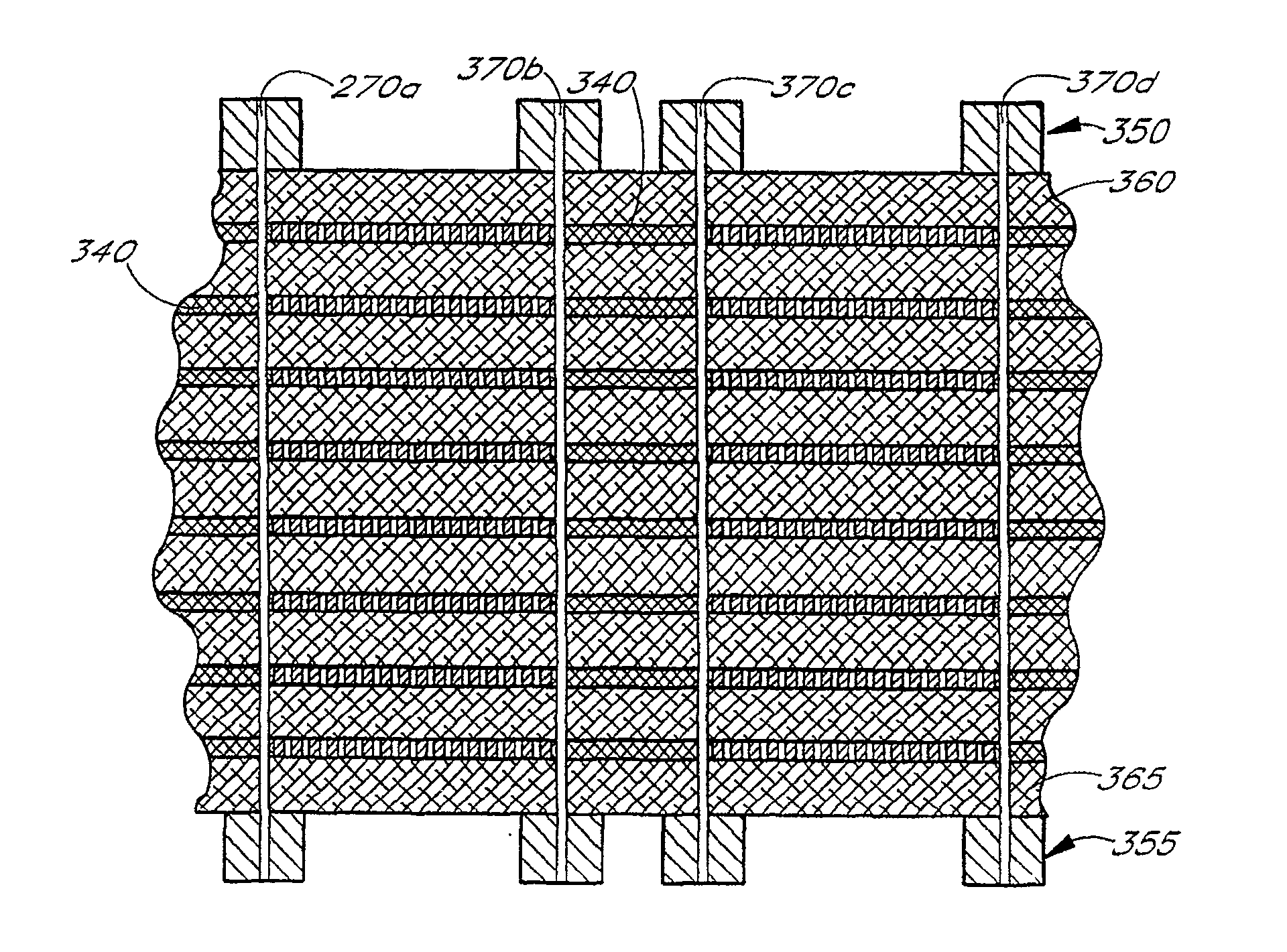
采用铁磁金属用于磁芯材料的本发明的一个实施例的制造示于图14—18中,其中柔性电路或印制电路板290支撑形成在FLEX或PCB上并由绝缘层分开的一系列层叠薄金属圆环。圆环的中心和外部的镀覆穿孔和镀覆完成围绕磁芯的电气绕线。如下所述,通过显著减小每个叠层磁芯截面的横截面面积,这个实施例显著地最小化了涡流。The fabrication of an embodiment of the invention employing ferromagnetic metals for the core material is shown in FIGS. Laminated thin metal rings. Plated piercings and plating in the center and outside of the ring complete the electrical winding around the core. As described below, this embodiment significantly minimizes eddy currents by significantly reducing the cross-sectional area of each laminated core section.
通过首先在PCB或FLEX290上层叠铁磁金属片,然后刻蚀掉部分铁磁片以形成多个紧密排列的、窄的连续磁芯段的图形,形成多个磁芯叠层。这样,图14示出了具有16个被刻蚀磁芯阵列的PCB或FLEX310的单个层。应该理解本领域中公知的层叠和刻蚀工艺一般允许制造16个以上的这种阵列,这取决于阵列和图形的尺寸。有利地,采用公知的双面工艺刻蚀磁芯阵列315,以便在片310的顶部和底部形成相同的阵列。Multiple core stacks are formed by first laminating ferromagnetic metal sheets on a PCB or FLEX290, and then etching away portions of the ferromagnetic sheets to form a pattern of closely spaced, narrow contiguous core segments. Thus, Figure 14 shows a single layer of a PCB or
单个磁芯阵列315的放大图示于图15中,该图示出了具有16个同心铁磁导电金属环320a—320p的阵列,这些金属环通过各个被刻蚀的间隔或空隙325a-325o而互相绝缘。同样,阵列315外部的区域330和最内部环320内部的区域335没有磁性材料。然而,本发明不限于同心环阵列,对于本领域技术人员来说很显然可以构成其它磁芯阵列,如互相绝缘的一系列连续更大的正方形或矩形形状。An enlarged view of a single
下一制造步骤是将多个PCB和FLEX层310基本上对准地与阵列315堆叠起来。如图16A中所示,同心环315a-315h的磁芯阵列安装每层上的磁芯图形对准的方式一个一个堆叠在一起。结果是制造了具有非常小的涡流面积的多个高磁通承载金属磁芯。这样,用于刻蚀阵列315的原片可以是非常薄的,通常在0.0005”到0.010”英寸范围内。可以采用传统的PCB或FLEX(FPC)刻蚀技术将同心环刻蚀到在0.002”-0.003”量级上的非常窄的宽度。结果是,关于磁芯的横截面涡流产生的区域,大大减小了尺寸。The next fabrication step is to stack the multiple PCB and
作为部分堆叠工艺,薄层绝缘材料340与每个被刻蚀同心环阵列315的顶表面相邻设置。通常,采用环氧树脂材料。这种绝缘片和支撑被刻蚀铁磁环的绝缘片可以是不同材料的。代表性材料包括由Dupont和Rogers Corp制造的用于制造PCB板和FLEX的环氧树脂和丙烯酸(acrylics)。环氧树脂和胶片(具有玻璃的环氧树脂)一般用于构成PCB板,丙烯酸一般用于制造FLEX。在层叠工艺期间,图15中所示的间隙325、间隙330和间隙335用绝缘材料340填充,如图18A和18B所示。As part of the stacking process, a thin layer of insulating
如上所述,通过与磁芯结构两侧上与印制电路接触的导电穿孔,有利地提供本发明的优选实施例电气绕线。用于图14—18的实施例的绕线的制造步骤示于图17A、17B、18A和18B中。As noted above, the preferred embodiment electrical windings of the present invention are advantageously provided through conductive vias in contact with the printed circuit on both sides of the core structure. The manufacturing steps for the windings for the embodiment of Figures 14-18 are shown in Figures 17A, 17B, 18A and 18B.
参见图17A和17B,附加铜层350、355分别层叠在顶表面和底表面上,而两个附加绝缘层360、365将铜表面与被刻蚀金属表面分开。Referring to Figures 17A and 17B,
图18A和18B中示出了具有通过整个层叠阵列钻成的穿孔370的完成结构。这些穿孔位于低电阻率铁磁环附近但不与其接触,以便电绝缘由镀覆穿孔提供的绕线匝。然后用导电材料、(通常为铜)镀覆这些孔370。也可以采用在穿孔内的导电墨水和导电膏。然后刻蚀铜层350、355以便形成与镀覆穿孔370电接触的电路图形,用于形成围绕同心环磁芯阵列315的绕线。The completed structure with
为了清楚示出,图18A和18B中所示的实施例表示每个变压器的少量穿孔370a,370b,370c,和370d。对于本领域普通技术人员来说很显然图14—18的实施例可以通过添加附加穿孔而具有多个绕线。如果需要,附加铜层可以叠置在层350、355上以提供到附加穿孔的所需连接。For clarity of illustration, the embodiment shown in Figures 18A and 18B shows a small number of perforations 370a, 370b, 370c, and 370d per transformer. It will be apparent to those of ordinary skill in the art that the embodiment of Figures 14-18 can have multiple windings by adding additional perforations. If desired, additional copper layers may be overlaid on
可通过“冲模”(die)切割或从阵列选择部件的常用方法从图18A和18B中的层叠阵列中抽取单个变压器和电感器器件。每个这种器件可用于替代图1—13中所示的传统电感器件。而且,由于刻蚀金属磁芯是阵列的一部分,如图16中所示,因此可以互连到其它元件。Individual transformer and inductor devices can be extracted from the stacked arrays in Figures 18A and 18B by "die" cutting or the usual method of selecting components from the array. Each of these devices can be used to replace the conventional inductive devices shown in Figures 1-13. Also, since the etched metal core is part of the array, as shown in Figure 16, it can be interconnected to other components.
优选实施例的优点Advantages of the preferred embodiment
一片磁芯:A core:
在E形磁芯结构中,如图1所示,不可避免地在E形磁芯和帽之间形成间隙。大多数变压器采用要求采用例如环氧树脂和夹子将一半磁芯连接到其它磁芯上的E型磁芯。这些工艺是耗时的、造成损失和由于E形磁芯和帽之间形成的间隙而使器件参数变化。相比较而言,本发明的优选实施例的磁芯是连续片的,由此提供改进的变压器效率。一片设计不再需要在分离处理步骤中将两个分立片连接在一起。In the E-shaped magnetic core structure, as shown in Fig. 1, a gap is inevitably formed between the E-shaped magnetic core and the cap. Most transformers use E-cores that require the use of, for example, epoxy and clips to attach one half of the core to the other. These processes are time consuming, lossy and cause device parameter variations due to the gap formed between the E-shaped core and cap. In comparison, the magnetic core of the preferred embodiment of the present invention is a continuous sheet, thereby providing improved transformer efficiency. One-piece designs eliminate the need to join two discrete pieces together in a separate processing step.
如果希望在图14—18的实施例中有意形成间隙以避免磁饱和,可以在图15中所示的同心环中刻蚀形成间隔。这种被刻蚀间隙环消除了E形芯的传统机械分隔的大变化。If it is desired to intentionally form a gap in the embodiment of FIGS. 14-18 to avoid magnetic saturation, a space can be etched in the concentric rings shown in FIG. 15 . This etched spacer ring eliminates the large variation in traditional mechanical separation of E-shaped cores.
减少了涡流:Reduced eddy currents:
按照图14—18的方式构成的电感器和变压器通过在两个方向分隔金属叠层可提供具有很少涡流的优异性能。产生这个结果是因为所示优选实施例借助(a)由其刻蚀环320的金属片可以是比采用PCB或FLEX制造材料更薄(b)单个绝缘环320可以制成为非常窄而具有比传统层叠磁芯薄的磁芯。由于涡流与段的横截面面积的平方成正比,因此与制造变压器或电感器的传统方法相比优选实施例显著地减少了涡流。例如,参照图1中所示的传统E形磁芯,这种磁芯的金属叠层不能在两个方向分开,因为条会散开或简单地说不具有机械整体性。Inductors and transformers constructed in the manner of Figures 14-18 provide excellent performance with very little eddy current by separating the metal stack in both directions. This result occurs because the preferred embodiment shown by virtue of (a) the metal sheet from which the ring 320 is etched can be thinner than with PCB or FLEX manufacturing materials (b) a single insulating ring 320 can be made very narrow with a thinner thickness than conventional Laminated cores are thin cores. Since eddy currents are proportional to the square of the cross-sectional area of a segment, preferred embodiments significantly reduce eddy currents compared to conventional methods of manufacturing transformers or inductors. For example, referring to the conventional E-shaped core shown in Figure 1, the metal laminations of such a core cannot be separated in two directions because the strips would fall apart or simply not have mechanical integrity.
表面安装:Surface mount:
根据本发明优选实施例形成的绕线可以在不需要分开的引线框架结构、复杂管脚或最终镀覆的情况下形成为表面安装引线。Wire wraps formed in accordance with preferred embodiments of the present invention can be formed as surface mount leads without the need for separate lead frame structures, complex pinouts, or final plating.
互连:interconnection:
由于刻蚀变压器/电感器是采用与制造PCB或FPC的相同工艺制造的,因此变压器可以有利地成为电源或电路组件的集成部件,由此减小物理尺寸,减少接点,和通常使组件更紧凑和更小。电路元件可以直接设置在被刻蚀变压器的上面或下面,用变压器的区域作为用于平衡电路的载体,以便整个电路的面积将与变压器面积一样小。Since etched transformers/inductors are fabricated using the same process used to fabricate PCBs or FPCs, transformers can advantageously be an integrated part of a power supply or circuit assembly, thereby reducing physical size, reducing joints, and generally making the assembly more compact and smaller. Circuit elements can be placed directly above or below the etched transformer, using the area of the transformer as a carrier for the balanced circuit so that the overall circuit area will be as small as the transformer area.
磁性噪声:Magnetic noise:
根据优选实施例构成的磁芯提供具有损失比传统变压器少的更有效的磁通路径。这些特性在设计和功能上更类似于环。磁通路径短于采用传统磁芯如E—磁芯和PQ磁芯的可比变压器。A magnetic core constructed in accordance with a preferred embodiment provides a more efficient flux path with less loss than conventional transformers. These features are more similar to rings in design and function. The flux paths are shorter than comparable transformers using conventional cores such as E-cores and PQ cores.
尺寸:size:
优选实施例可以做得更小,因为它们不需要复杂的管脚或引线框架。顶表面和底表面上的表面焊盘形成它们自己的接点,并且它们可以直接表面安装到PCB上,由此减少器件着脚点和给其它元件留出更多的空间。绕线处于2个平面内,因此通常使用的十(10)层平面变压器器件的绕线可在总高度上减少五(5)倍。“磁芯”处于一个平面内代替三维E形磁芯结构,进一步大大减少了总高度。Preferred embodiments can be made smaller since they do not require complex pins or lead frames. The surface pads on the top and bottom surfaces form their own contacts, and they can be surface mounted directly to the PCB, thereby reducing device footprint and leaving more space for other components. The windings are in 2 planes, so the windings of a commonly used ten (10) layer planar transformer device can be reduced by a factor of five (5) in overall height. The "magnetic core" is in one plane instead of the three-dimensional E-shaped magnetic core structure, which further greatly reduces the overall height.
成本:cost:
优选实施例可以由柔性电路制成并可以比多层平面绕线更便宜地制造。而且不再需要引线框架、封装、和帽粘接,由此使器件更容易制造。Preferred embodiments may be made from flex circuits and may be less expensive to manufacture than multilayer planar wires. Also lead frame, package, and cap bonding are no longer required, thereby making the device easier to manufacture.
散热性能:Thermal performance:
根据本发明优选实施例构成的电感器和变压器的显著优点是产热绕线不埋置在组件内或互相缠绕在每个绕线的顶部,如传统变压器那样,而且它们不需要像平面变压器那样叠置在一起。代替地,镀覆绕线基本上位于变压器或电感器器件的顶面和底面。这种布置提供优异的散热性能而不会将热量收集掩埋在绕线内。只通过通常只有0.005英寸厚的薄焊接掩膜,将绕线的一半放置成与散热片热接触,可以将PCB有利地固定到散热片上,由此提供优异的表面面积与热量比。图12示出了用于优异散热性能的安装到如铜和铝的散热片232上的大表面面积230的一个例子。A significant advantage of inductors and transformers constructed in accordance with preferred embodiments of the present invention is that the heat producing windings are not embedded within the assembly or intertwined on top of each winding, as in conventional transformers, and they do not need to be as in planar transformers. Stacked together. Instead, plated windings are located substantially on the top and bottom surfaces of the transformer or inductor device. This arrangement provides excellent heat dissipation without burying heat collection within the windings. The PCB is advantageously secured to the heat sink by placing half of the wirewrap in thermal contact with the heat sink only through a thin solder mask, typically only 0.005 inches thick, thereby providing an excellent surface area to heat ratio. Figure 12 shows an example of a
前面已经参照一些优选实施例介绍了本发明,这些实施例仅是借助例子提供的,并不限制本发明的范围。因而,本发明的范围应该只根据所附权利要求书界定。The invention has been described above with reference to some preferred embodiments, which are provided by way of example only and do not limit the scope of the invention. Accordingly, the scope of the present invention should be defined only in accordance with the appended claims.
Claims (42)
Applications Claiming Priority (3)
| Application Number | Priority Date | Filing Date | Title |
|---|---|---|---|
| US23463600P | 2000-09-22 | 2000-09-22 | |
| US60/234,636 | 2000-09-22 | ||
| US60/237,356 | 2000-09-27 |
Related Parent Applications (1)
| Application Number | Title | Priority Date | Filing Date |
|---|---|---|---|
| CN01816181.2A Division CN1261753C (en) | 2000-09-22 | 2001-09-24 | Electronic transformer/inductor device and manufacturing method thereof |
Publications (2)
| Publication Number | Publication Date |
|---|---|
| CN1783367A CN1783367A (en) | 2006-06-07 |
| CN100511503C true CN100511503C (en) | 2009-07-08 |
Family
ID=36773380
Family Applications (1)
| Application Number | Title | Priority Date | Filing Date |
|---|---|---|---|
| CNB2005101257860A Expired - Fee Related CN100511503C (en) | 2000-09-22 | 2001-09-24 | Electronic transformer/inductor devices and methods for making same |
Country Status (1)
| Country | Link |
|---|---|
| CN (1) | CN100511503C (en) |
Cited By (1)
| Publication number | Priority date | Publication date | Assignee | Title |
|---|---|---|---|---|
| CN102301435A (en) * | 2009-07-15 | 2011-12-28 | 脉冲电子(新加坡)私人有限公司 | Substrate Inductive Devices And Methods |
Families Citing this family (4)
| Publication number | Priority date | Publication date | Assignee | Title |
|---|---|---|---|---|
| CN101924102B (en) * | 2009-06-15 | 2013-07-31 | 慧国(上海)软件科技有限公司 | Semiconductor device |
| CN110112121A (en) * | 2019-04-29 | 2019-08-09 | 中国电子科技集团公司第十三研究所 | Embedded, electromagnetism Manufacturing resource passive network, semiconductor devices and electronic system |
| US12347597B2 (en) * | 2021-03-23 | 2025-07-01 | Tdk Corporation | Multi-layer inductor |
| CN119694731B (en) * | 2025-02-25 | 2025-06-20 | 东南大学 | Virtual magnetic core constructed by using vector magnetic circuit principle and its application method |
-
2001
- 2001-09-24 CN CNB2005101257860A patent/CN100511503C/en not_active Expired - Fee Related
Cited By (2)
| Publication number | Priority date | Publication date | Assignee | Title |
|---|---|---|---|---|
| CN102301435A (en) * | 2009-07-15 | 2011-12-28 | 脉冲电子(新加坡)私人有限公司 | Substrate Inductive Devices And Methods |
| CN102301435B (en) * | 2009-07-15 | 2014-12-24 | 脉冲电子(新加坡)私人有限公司 | Substrate inductance device and method |
Also Published As
| Publication number | Publication date |
|---|---|
| CN1783367A (en) | 2006-06-07 |
Similar Documents
| Publication | Publication Date | Title |
|---|---|---|
| CN1261753C (en) | Electronic transformer/inductor device and manufacturing method thereof | |
| CN100530455C (en) | Electronic transformer/inductor devices and methods for making same | |
| US8941457B2 (en) | Miniature power inductor and methods of manufacture | |
| KR101792281B1 (en) | Power Inductor and Manufacturing Method for the Same | |
| US7253711B2 (en) | Embedded toroidal inductors | |
| KR101883036B1 (en) | Multilayered electronic component and multilayered chip antenna comprising the same | |
| CN100511503C (en) | Electronic transformer/inductor devices and methods for making same | |
| KR20010114120A (en) | PCB Inductor and Transformer using the PCB Inductor | |
| TW580712B (en) | Electronic transformer/inductor devices and methods for making same | |
| JP2002008922A (en) | Coil part | |
| HK1079896B (en) | Electronic transformer/inductor devices and methods for making same |
Legal Events
| Date | Code | Title | Description |
|---|---|---|---|
| C06 | Publication | ||
| PB01 | Publication | ||
| C10 | Entry into substantive examination | ||
| SE01 | Entry into force of request for substantive examination | ||
| C14 | Grant of patent or utility model | ||
| GR01 | Patent grant | ||
| C56 | Change in the name or address of the patentee |
Owner name: DUOJINGXIAN ELECTRONICS CO.,LTD. Free format text: FORMER NAME: M-FOLAIKES REFINED LINE ELECTRONICS CO.,LTD. |
|
| CP03 | Change of name, title or address |
Address after: American California Patentee after: Flex Multi Fineline Electronix Address before: American California Patentee before: Flex Multi Fineline Electronix |
|
| C17 | Cessation of patent right | ||
| CF01 | Termination of patent right due to non-payment of annual fee |
Granted publication date: 20090708 Termination date: 20100924 |