CN100477235C - Method for forming semiconductor device - Google Patents
Method for forming semiconductor device Download PDFInfo
- Publication number
- CN100477235C CN100477235C CNB2005800358985A CN200580035898A CN100477235C CN 100477235 C CN100477235 C CN 100477235C CN B2005800358985 A CNB2005800358985 A CN B2005800358985A CN 200580035898 A CN200580035898 A CN 200580035898A CN 100477235 C CN100477235 C CN 100477235C
- Authority
- CN
- China
- Prior art keywords
- silicon
- area
- semiconductor device
- substrate
- layer
- Prior art date
- Legal status (The legal status is an assumption and is not a legal conclusion. Google has not performed a legal analysis and makes no representation as to the accuracy of the status listed.)
- Active
Links
- 239000004065 semiconductor Substances 0.000 title claims abstract description 51
- 238000000034 method Methods 0.000 title claims abstract description 40
- 229910052710 silicon Inorganic materials 0.000 claims abstract description 117
- 239000010703 silicon Substances 0.000 claims abstract description 117
- XUIMIQQOPSSXEZ-UHFFFAOYSA-N Silicon Chemical compound [Si] XUIMIQQOPSSXEZ-UHFFFAOYSA-N 0.000 claims abstract description 112
- 239000000758 substrate Substances 0.000 claims abstract description 68
- 239000013078 crystal Substances 0.000 claims abstract description 53
- 230000015572 biosynthetic process Effects 0.000 claims description 24
- 230000004888 barrier function Effects 0.000 claims description 22
- 229910021332 silicide Inorganic materials 0.000 claims description 10
- FVBUAEGBCNSCDD-UHFFFAOYSA-N silicide(4-) Chemical compound [Si-4] FVBUAEGBCNSCDD-UHFFFAOYSA-N 0.000 claims description 10
- 150000003376 silicon Chemical class 0.000 claims description 9
- 239000011810 insulating material Substances 0.000 claims description 4
- 238000001802 infusion Methods 0.000 claims 1
- 239000012212 insulator Substances 0.000 abstract description 7
- 238000005516 engineering process Methods 0.000 description 29
- 239000007943 implant Substances 0.000 description 22
- 238000005530 etching Methods 0.000 description 17
- 229910052581 Si3N4 Inorganic materials 0.000 description 16
- HQVNEWCFYHHQES-UHFFFAOYSA-N silicon nitride Chemical compound N12[Si]34N5[Si]62N3[Si]51N64 HQVNEWCFYHHQES-UHFFFAOYSA-N 0.000 description 16
- 229910052751 metal Inorganic materials 0.000 description 15
- 239000002184 metal Substances 0.000 description 15
- 239000002019 doping agent Substances 0.000 description 14
- VYPSYNLAJGMNEJ-UHFFFAOYSA-N Silicium dioxide Chemical compound O=[Si]=O VYPSYNLAJGMNEJ-UHFFFAOYSA-N 0.000 description 13
- 239000011248 coating agent Substances 0.000 description 11
- 238000000576 coating method Methods 0.000 description 11
- 238000002513 implantation Methods 0.000 description 10
- 235000012431 wafers Nutrition 0.000 description 8
- 238000000151 deposition Methods 0.000 description 7
- 150000004767 nitrides Chemical class 0.000 description 6
- 238000001259 photo etching Methods 0.000 description 6
- 239000000377 silicon dioxide Substances 0.000 description 6
- 238000005229 chemical vapour deposition Methods 0.000 description 5
- 230000008021 deposition Effects 0.000 description 5
- -1 oxonium ion Chemical class 0.000 description 5
- 229920002120 photoresistant polymer Polymers 0.000 description 5
- 125000006850 spacer group Chemical group 0.000 description 5
- KRHYYFGTRYWZRS-UHFFFAOYSA-N Fluorane Chemical compound F KRHYYFGTRYWZRS-UHFFFAOYSA-N 0.000 description 4
- 238000011049 filling Methods 0.000 description 4
- 239000010408 film Substances 0.000 description 4
- 239000007789 gas Substances 0.000 description 4
- 150000002500 ions Chemical class 0.000 description 4
- BLRPTPMANUNPDV-UHFFFAOYSA-N Silane Chemical compound [SiH4] BLRPTPMANUNPDV-UHFFFAOYSA-N 0.000 description 3
- BOTDANWDWHJENH-UHFFFAOYSA-N Tetraethyl orthosilicate Chemical compound CCO[Si](OCC)(OCC)OCC BOTDANWDWHJENH-UHFFFAOYSA-N 0.000 description 3
- QVGXLLKOCUKJST-UHFFFAOYSA-N atomic oxygen Chemical compound [O] QVGXLLKOCUKJST-UHFFFAOYSA-N 0.000 description 3
- 230000008901 benefit Effects 0.000 description 3
- 238000009792 diffusion process Methods 0.000 description 3
- 230000006872 improvement Effects 0.000 description 3
- 238000009413 insulation Methods 0.000 description 3
- 239000000203 mixture Substances 0.000 description 3
- 230000003647 oxidation Effects 0.000 description 3
- 238000007254 oxidation reaction Methods 0.000 description 3
- 239000001301 oxygen Substances 0.000 description 3
- 229910052760 oxygen Inorganic materials 0.000 description 3
- 238000000059 patterning Methods 0.000 description 3
- 229910000077 silane Inorganic materials 0.000 description 3
- RPAJSBKBKSSMLJ-DFWYDOINSA-N (2s)-2-aminopentanedioic acid;hydrochloride Chemical compound Cl.OC(=O)[C@@H](N)CCC(O)=O RPAJSBKBKSSMLJ-DFWYDOINSA-N 0.000 description 2
- 101100373011 Drosophila melanogaster wapl gene Proteins 0.000 description 2
- PXHVJJICTQNCMI-UHFFFAOYSA-N Nickel Chemical compound [Ni] PXHVJJICTQNCMI-UHFFFAOYSA-N 0.000 description 2
- NBIIXXVUZAFLBC-UHFFFAOYSA-N Phosphoric acid Chemical compound OP(O)(O)=O NBIIXXVUZAFLBC-UHFFFAOYSA-N 0.000 description 2
- 238000004026 adhesive bonding Methods 0.000 description 2
- 238000000137 annealing Methods 0.000 description 2
- 229910052785 arsenic Inorganic materials 0.000 description 2
- RQNWIZPPADIBDY-UHFFFAOYSA-N arsenic atom Chemical compound [As] RQNWIZPPADIBDY-UHFFFAOYSA-N 0.000 description 2
- 238000001505 atmospheric-pressure chemical vapour deposition Methods 0.000 description 2
- 230000008859 change Effects 0.000 description 2
- 238000006243 chemical reaction Methods 0.000 description 2
- 125000001475 halogen functional group Chemical group 0.000 description 2
- 238000010438 heat treatment Methods 0.000 description 2
- 238000009434 installation Methods 0.000 description 2
- 239000012774 insulation material Substances 0.000 description 2
- 229910021421 monocrystalline silicon Inorganic materials 0.000 description 2
- 230000003071 parasitic effect Effects 0.000 description 2
- 210000004483 pasc Anatomy 0.000 description 2
- 238000001020 plasma etching Methods 0.000 description 2
- 239000000126 substance Substances 0.000 description 2
- DDFHBQSCUXNBSA-UHFFFAOYSA-N 5-(5-carboxythiophen-2-yl)thiophene-2-carboxylic acid Chemical compound S1C(C(=O)O)=CC=C1C1=CC=C(C(O)=O)S1 DDFHBQSCUXNBSA-UHFFFAOYSA-N 0.000 description 1
- ZOXJGFHDIHLPTG-UHFFFAOYSA-N Boron Chemical compound [B] ZOXJGFHDIHLPTG-UHFFFAOYSA-N 0.000 description 1
- UFHFLCQGNIYNRP-UHFFFAOYSA-N Hydrogen Chemical compound [H][H] UFHFLCQGNIYNRP-UHFFFAOYSA-N 0.000 description 1
- CBENFWSGALASAD-UHFFFAOYSA-N Ozone Chemical compound [O-][O+]=O CBENFWSGALASAD-UHFFFAOYSA-N 0.000 description 1
- RTAQQCXQSZGOHL-UHFFFAOYSA-N Titanium Chemical compound [Ti] RTAQQCXQSZGOHL-UHFFFAOYSA-N 0.000 description 1
- 229910000147 aluminium phosphate Inorganic materials 0.000 description 1
- 238000013459 approach Methods 0.000 description 1
- 229910052796 boron Inorganic materials 0.000 description 1
- 230000003139 buffering effect Effects 0.000 description 1
- 239000003990 capacitor Substances 0.000 description 1
- 239000012159 carrier gas Substances 0.000 description 1
- 239000003795 chemical substances by application Substances 0.000 description 1
- 229910017052 cobalt Inorganic materials 0.000 description 1
- 239000010941 cobalt Substances 0.000 description 1
- GUTLYIVDDKVIGB-UHFFFAOYSA-N cobalt atom Chemical compound [Co] GUTLYIVDDKVIGB-UHFFFAOYSA-N 0.000 description 1
- 238000010168 coupling process Methods 0.000 description 1
- 238000005859 coupling reaction Methods 0.000 description 1
- OKZIUSOJQLYFSE-UHFFFAOYSA-N difluoroboron Chemical compound F[B]F OKZIUSOJQLYFSE-UHFFFAOYSA-N 0.000 description 1
- 230000005669 field effect Effects 0.000 description 1
- 239000001257 hydrogen Substances 0.000 description 1
- 229910052739 hydrogen Inorganic materials 0.000 description 1
- GPRLSGONYQIRFK-UHFFFAOYSA-N hydron Chemical compound [H+] GPRLSGONYQIRFK-UHFFFAOYSA-N 0.000 description 1
- 238000002955 isolation Methods 0.000 description 1
- 238000004518 low pressure chemical vapour deposition Methods 0.000 description 1
- 239000000463 material Substances 0.000 description 1
- 229910044991 metal oxide Inorganic materials 0.000 description 1
- 150000004706 metal oxides Chemical class 0.000 description 1
- 229910052759 nickel Inorganic materials 0.000 description 1
- 229910021420 polycrystalline silicon Inorganic materials 0.000 description 1
- 229920005591 polysilicon Polymers 0.000 description 1
- 229920001296 polysiloxane Polymers 0.000 description 1
- 230000008569 process Effects 0.000 description 1
- 230000001737 promoting effect Effects 0.000 description 1
- 230000001105 regulatory effect Effects 0.000 description 1
- 238000000926 separation method Methods 0.000 description 1
- 229910052814 silicon oxide Inorganic materials 0.000 description 1
- 230000008961 swelling Effects 0.000 description 1
- 239000010409 thin film Substances 0.000 description 1
- 239000010936 titanium Substances 0.000 description 1
- 229910052719 titanium Inorganic materials 0.000 description 1
Images


Classifications
-
- H—ELECTRICITY
- H01—ELECTRIC ELEMENTS
- H01L—SEMICONDUCTOR DEVICES NOT COVERED BY CLASS H10
- H01L29/00—Semiconductor devices specially adapted for rectifying, amplifying, oscillating or switching and having potential barriers; Capacitors or resistors having potential barriers, e.g. a PN-junction depletion layer or carrier concentration layer; Details of semiconductor bodies or of electrodes thereof ; Multistep manufacturing processes therefor
- H01L29/66—Types of semiconductor device ; Multistep manufacturing processes therefor
- H01L29/66007—Multistep manufacturing processes
- H01L29/66075—Multistep manufacturing processes of devices having semiconductor bodies comprising group 14 or group 13/15 materials
- H01L29/66227—Multistep manufacturing processes of devices having semiconductor bodies comprising group 14 or group 13/15 materials the devices being controllable only by the electric current supplied or the electric potential applied, to an electrode which does not carry the current to be rectified, amplified or switched, e.g. three-terminal devices
- H01L29/66409—Unipolar field-effect transistors
- H01L29/66477—Unipolar field-effect transistors with an insulated gate, i.e. MISFET
- H01L29/66742—Thin film unipolar transistors
- H01L29/66772—Monocristalline silicon transistors on insulating substrates, e.g. quartz substrates
-
- H—ELECTRICITY
- H01—ELECTRIC ELEMENTS
- H01L—SEMICONDUCTOR DEVICES NOT COVERED BY CLASS H10
- H01L27/00—Devices consisting of a plurality of semiconductor or other solid-state components formed in or on a common substrate
- H01L27/02—Devices consisting of a plurality of semiconductor or other solid-state components formed in or on a common substrate including semiconductor components specially adapted for rectifying, oscillating, amplifying or switching and having potential barriers; including integrated passive circuit elements having potential barriers
- H01L27/12—Devices consisting of a plurality of semiconductor or other solid-state components formed in or on a common substrate including semiconductor components specially adapted for rectifying, oscillating, amplifying or switching and having potential barriers; including integrated passive circuit elements having potential barriers the substrate being other than a semiconductor body, e.g. an insulating body
-
- H—ELECTRICITY
- H01—ELECTRIC ELEMENTS
- H01L—SEMICONDUCTOR DEVICES NOT COVERED BY CLASS H10
- H01L21/00—Processes or apparatus adapted for the manufacture or treatment of semiconductor or solid state devices or of parts thereof
- H01L21/70—Manufacture or treatment of devices consisting of a plurality of solid state components formed in or on a common substrate or of parts thereof; Manufacture of integrated circuit devices or of parts thereof
- H01L21/77—Manufacture or treatment of devices consisting of a plurality of solid state components or integrated circuits formed in, or on, a common substrate
- H01L21/78—Manufacture or treatment of devices consisting of a plurality of solid state components or integrated circuits formed in, or on, a common substrate with subsequent division of the substrate into plural individual devices
- H01L21/82—Manufacture or treatment of devices consisting of a plurality of solid state components or integrated circuits formed in, or on, a common substrate with subsequent division of the substrate into plural individual devices to produce devices, e.g. integrated circuits, each consisting of a plurality of components
- H01L21/84—Manufacture or treatment of devices consisting of a plurality of solid state components or integrated circuits formed in, or on, a common substrate with subsequent division of the substrate into plural individual devices to produce devices, e.g. integrated circuits, each consisting of a plurality of components the substrate being other than a semiconductor body, e.g. being an insulating body
-
- H—ELECTRICITY
- H01—ELECTRIC ELEMENTS
- H01L—SEMICONDUCTOR DEVICES NOT COVERED BY CLASS H10
- H01L27/00—Devices consisting of a plurality of semiconductor or other solid-state components formed in or on a common substrate
- H01L27/02—Devices consisting of a plurality of semiconductor or other solid-state components formed in or on a common substrate including semiconductor components specially adapted for rectifying, oscillating, amplifying or switching and having potential barriers; including integrated passive circuit elements having potential barriers
- H01L27/12—Devices consisting of a plurality of semiconductor or other solid-state components formed in or on a common substrate including semiconductor components specially adapted for rectifying, oscillating, amplifying or switching and having potential barriers; including integrated passive circuit elements having potential barriers the substrate being other than a semiconductor body, e.g. an insulating body
- H01L27/1203—Devices consisting of a plurality of semiconductor or other solid-state components formed in or on a common substrate including semiconductor components specially adapted for rectifying, oscillating, amplifying or switching and having potential barriers; including integrated passive circuit elements having potential barriers the substrate being other than a semiconductor body, e.g. an insulating body the substrate comprising an insulating body on a semiconductor body, e.g. SOI
-
- H—ELECTRICITY
- H01—ELECTRIC ELEMENTS
- H01L—SEMICONDUCTOR DEVICES NOT COVERED BY CLASS H10
- H01L29/00—Semiconductor devices specially adapted for rectifying, amplifying, oscillating or switching and having potential barriers; Capacitors or resistors having potential barriers, e.g. a PN-junction depletion layer or carrier concentration layer; Details of semiconductor bodies or of electrodes thereof ; Multistep manufacturing processes therefor
- H01L29/02—Semiconductor bodies ; Multistep manufacturing processes therefor
- H01L29/04—Semiconductor bodies ; Multistep manufacturing processes therefor characterised by their crystalline structure, e.g. polycrystalline, cubic or particular orientation of crystalline planes
- H01L29/045—Semiconductor bodies ; Multistep manufacturing processes therefor characterised by their crystalline structure, e.g. polycrystalline, cubic or particular orientation of crystalline planes by their particular orientation of crystalline planes
-
- H—ELECTRICITY
- H01—ELECTRIC ELEMENTS
- H01L—SEMICONDUCTOR DEVICES NOT COVERED BY CLASS H10
- H01L29/00—Semiconductor devices specially adapted for rectifying, amplifying, oscillating or switching and having potential barriers; Capacitors or resistors having potential barriers, e.g. a PN-junction depletion layer or carrier concentration layer; Details of semiconductor bodies or of electrodes thereof ; Multistep manufacturing processes therefor
- H01L29/66—Types of semiconductor device ; Multistep manufacturing processes therefor
- H01L29/68—Types of semiconductor device ; Multistep manufacturing processes therefor controllable by only the electric current supplied, or only the electric potential applied, to an electrode which does not carry the current to be rectified, amplified or switched
- H01L29/76—Unipolar devices, e.g. field effect transistors
- H01L29/772—Field effect transistors
- H01L29/78—Field effect transistors with field effect produced by an insulated gate
- H01L29/786—Thin film transistors, i.e. transistors with a channel being at least partly a thin film
- H01L29/78651—Silicon transistors
- H01L29/78654—Monocrystalline silicon transistors
Landscapes
- Engineering & Computer Science (AREA)
- Power Engineering (AREA)
- Microelectronics & Electronic Packaging (AREA)
- General Physics & Mathematics (AREA)
- Physics & Mathematics (AREA)
- Computer Hardware Design (AREA)
- Condensed Matter Physics & Semiconductors (AREA)
- Ceramic Engineering (AREA)
- Manufacturing & Machinery (AREA)
- Chemical & Material Sciences (AREA)
- Crystallography & Structural Chemistry (AREA)
- Thin Film Transistor (AREA)
- Element Separation (AREA)
- Metal-Oxide And Bipolar Metal-Oxide Semiconductor Integrated Circuits (AREA)
- Recrystallisation Techniques (AREA)
Abstract
A semiconductor device comprising a substrate having a first crystal orientation and an insulating layer overlying the substrate is provided. A plurality of silicon layers are formed overlying the insulating layer. A first silicon layer comprises silicon having the first crystal orientation and a second silicon layer comprises silicon having a second crystal orientation. In addition, a method of forming a semiconductor device providing a silicon-on-insulator structure comprising a substrate with a silicon layer overlying the substrate and a first insulating layer interposed therebetween is provided. An opening is formed in a first region of the silicon-on-insulator structure by removing a portion of the silicon layer and the first insulating layer to expose a portion of the substrate layer. Selective epitaxial silicon is grown in the opening. A second insulating layer is formed in the silicon grown in the opening to provide an insulating layer between the grown silicon in the opening and the substrate.
Description
Technical field
The present invention is relevant semiconductor device and the method for making semiconductor device, especially relevant silicon-on-insulator (silicon-on-insulator, SOI) improved semiconductor device of technology of comprising.
Background technology
The important goal that semiconductor industry is studied is for promoting the electrical source consumption that semiconducting behavior reduces semiconductor device simultaneously.Planar transistor, (MOSFETs) is particularly suitable for being used in high density integrated circuit as metal oxide semiconductcor field effect transistor.When the size (size) of MOSFET and other device when reducing, the regions and source of device, channel region, and the size (dimension) of gate electrode (gate electrode) also reduce.
Having the littler again planar transistor design of short channel length makes it that very shallow source/drain joint (shallow source/drain junction) need be set.Shallow joint for necessary with the dopant sideways diffusion (lateral diffusion) avoiding implanting to raceway groove, because this kind diffusion can cause leakage current and bad anti-destructive characteristics unfriendly.Acceptable performance for short channel devices need have 1000 usually
Or the shallow source/drain of the thickness of littler grade engages.
Silicon-on-insulator (SOI) technology can be facilitated high speed, shallow-coupling device.In addition, the SOI device passes through to reduce parasitic junction capacitance and improved performance.
In the SOI substrate, on monocrystalline silicon, form by the made flush type oxide of silica (buried oxide, BOX) film, and form monocrystalline silicon thin film thereon.The whole bag of tricks of making this kind SOI substrate is known person.(Separation-by-lmplanted Oxygen, SIMOX), wherein oxygen is for implanting in the monocrystalline substrate to form the ion of flush type oxide (BOX) film in order to pass through-to implant oxygen-separation for one of this kind method.
The another kind of method that forms the SOI substrate is the wafer combination, two Semiconductor substrate that wherein have a Si oxide superficial layer in the Si oxide surface combination together between two Semiconductor substrate, to form the BOX layer.
Another SOI technology is smart peeling (Smart Cut
 ), it is also contained via oxide skin(coating) in conjunction with first and second Semiconductor substrate.In the smart peeling method, before combination, implant first Semiconductor substrate with hydrogen ion earlier.This follow-up hydrionic implantation make implant hydrionic Semiconductor substrate from the substrate component of gluing from and stay one deck thin silicone layer gluing in second semiconductor substrate surface.
Performance of semiconductor devices can by have<110〉crystal orientation silicon on, but not known it<100〉crystal orientation silicon on, make P-type MOSFET (PMOSFET) and further promote 50% or more.Yet, with have<100〉crystal orientation silicon on formed NMOSFET compare down,<110〉performance of formed N-type MOSFET (NMOSFET) can be more bad on the silicon.
Performance of semiconductor devices also can be by at extremely thin silicon fiml, as has and make the MOSFET that exhausts (depleted) fully on the film of about 30nm or littler thickness and promoted.The MOSFET that exhausts fully provides the leakage current of minimizing and is the desired person of high performance device.Yet, be difficult to utilize known techniques, as adjusting the MOSFET limiting voltage (threshold voltage) that ring-type implant dosage (halo dose) change exhausts fully.The limiting voltage of wishing change MOSFET is with output height and low limiting voltage device.Comprise that the semiconductor device of the MOSFET with otherwise limit voltage range reduces the electrical source consumption of chip.
Used herein " semiconductor device (semiconductor devices) " speech is not limited to the example of specific exposure.Used herein semiconductor device comprise cover crystalline substance, cover crystalline substance/package assembling, electronic installation miscellaneous such as transistor, capacitor, microprocessor, random access memory.Generally speaking, semiconductor device is meant and comprises semi-conductive any electronic installation.
Summary of the invention
The semiconductor device technical field exists in conjunction with SOI technology and the improved properties need for equipment that exhausts the MOSFET technology fully.The semiconductor device technical field exist in conjunction with the SOI technology with on the same substrate in having on the different crystal orientations silicon improved properties need for equipment that forms MOSFET.In addition, this technical field exist provide a kind of combination S OI technology, fully exhaust the MOSFET technology, with on the same substrate in the demand that has on the different crystal orientations silicon semiconductor device that forms MOSFET.Moreover, exist in this technical field and to form the demand comprise SOI technology and the method for the semiconductor device that exhausts the MOSFET technology fully.This technical field also exist form comprise the SOI technology with on the same substrate in the demand of method with the semiconductor device that forms MOSFET on the different crystal orientations silicon.Moreover, this technical field exist form the SOI technology that comprises, fully exhaust the MOSFET technology, with on the same substrate in the demand of method with the semiconductor device that forms MOSFET on the different crystal orientations silicon.
Some instances conform these and other demand of the present invention, this example provide and comprise that the substrate with first crystal orientation reaches the semiconductor device of the insulating barrier on substrate.On insulating barrier, form a plurality of silicon layers.First silicon layer comprises the silicon with first crystal orientation and second silicon layer comprises the silicon with second crystal orientation.
Some example of the present invention further meets these and other demand, this example provides a kind of method that forms semiconductor device, comprise silicon on insulated substrate is provided, this silicon on insulated substrate comprises substrate, silicon layer this above substrate and first insulating barrier be inserted in therebetween.First area at silicon on insulated substrate forms perforate to a part by removing the silicon layer and first insulating barrier with a part that exposes substrate layer.Selective epitaxial silicon (epitaxial silicon) is grown in the perforate so far.Form second insulating barrier in the silicon in the perforate that grows in the first area between the silicon of in perforate, growing and the substrate insulating barrier to be set.
The present invention meets the improvement high-speed semiconductor need for equipment with improvement electrical characteristics.
Below present invention will be described in detail with reference to the accompanying, make address before the present invention other characteristics, aspect, and advantage become clear.
Description of drawings
Fig. 1 to 10 is that explanation has the formation that part depletion reaches the soi semiconductor device of the MOSFET that exhausts fully on same substrate;
Figure 11 A and 11B are that explanation has the formation that part depletion reaches the soi semiconductor device of the MOSFET that exhausts fully on same substrate;
Figure 12 to 14 is that explanation has the formation that part depletion reaches the soi semiconductor device of the MOSFET that exhausts fully on same substrate;
Figure 15 to 24 are explanations on the same substrate in the formation that has on the different crystal orientations silicon semiconductor device that forms MOSFET;
Figure 25 A and 25B be explanation on the same substrate in the formation that has on the different crystal orientations silicon semiconductor device that forms MOSFET;
Figure 26 to 28 are explanations on the same substrate in the formation that has on the different crystal orientations silicon semiconductor device that forms MOSFET;
Figure 29 is a kind of silicon on insulated substrate of explanation, and wherein silicon substrate comprises that the silicon layer with silicon-on-insulator is the silicon of different crystal orientations; And
Figure 30 be a kind of MOSFET technology that comprises soi process, exhausts fully of explanation, with on the same substrate in having on the different crystal orientations silicon semiconductor device that forms MOSFET.
Embodiment
The present invention can make to have SOI and exhausts the MOSFET technology fully, and/or on the same substrate in the improvement high-speed semiconductor device of benefit with the MOSFET that forms on the different crystal orientations silicon.The present invention further provides the advantage of utilizing the SOI technology to have to reduce parasitic junction capacitance by complete depletion technology and/or have the fair speed that PMOSFET provided that forms on the different crystal orientations silicon.
Below the formation of the semiconductor device that present invention will be described in detail with reference to the accompanying.Yet this only is an example, and the scope of patent protection that the present invention advocated is not limited to the formation of specific device illustrated in graphic.
At first explanation is formed on to have on the common SOI substrate and exhausts fully and the method for the semiconductor device of part depletion MOSFET.Soi structure 10 has silicon layer 16 and the insulating barrier 14 on substrate 12.Substrate 12 is generally silicon wafer.Insulating barrier 14 is flush type oxide (BOX) layer.Soi structure 10 shown in the 1st figure, can pass through known techniques, as SIMOX, and smart peeling, or the wafer combination technology is formed.Perhaps, the SOI wafer can derive from commercial source.In some example of the present invention, silicon layer 16 has about 30nm or littler thickness, by and can make the SOI device that exhausts fully.In some example of the present invention, BOX layer 14 has the thickness of about 50nm to about 400nm.In some example of the present invention, BOX layer 14 has the thickness of about 200nm to about 300nm.
As shown in Figure 2, on silicon layer 16, form oxide skin(coating) 18.Oxide skin(coating) 18 can be by being deposited as chemical vapor deposition (CVD), or the top surface of silicon layer 16 can give thermal oxidation.Subsequently silicon nitride film 20 is deposited on the oxide skin(coating) 18.In some example of the present invention, the thickness of oxide skin(coating) 18 is that about 5nm is to about 100nm.In some example of the present invention, oxide skin(coating) 18 is thick for about 20nm.Nitride layer 20 has the thickness of about 50nm to about 300nm.In some example of the present invention, the thickness of nitride layer 20 is about 100nm.
Then in soi structure 10, form perforate 22, as shown in Figure 3.In some example of the present invention, perforate 22 is formed with the upper surface 24 that exposes substrate 12 by known photoetching and etching technique.Known photoetching and etching technique are included on the soi structure 10 and form photoresist layer, make photoresist layer form mask and patterning, and anisotropic etching (anisotropicetch) soi structure 10 to be removing silicon nitride layer 20, oxide skin(coating) 18, silicon layer 16, and the part of BOX layer 14, and exposes the upper surface 24 of substrate 12.Then divest photoresist so that soi structure 10 as shown in Figure 3 to be provided.Known anisotropic etch techniques comprises plasma etching and reactive ion etching.This anisotropic etching can use the known variant layer of plasma selective etch of difference and alternately implement in a succession of plasma etch step mode.
Then on soi structure 10, deposit second silicon nitride layer 26, as shown in Figure 4.In some example of the present invention, silicon nitride layer 26 is by known deposition technique, is deposited into the thickness of about 10nm to about 100nm as CVD.Then anisotropic etching silicon nitride layer 26 is arranged in the side wall spacer (self-aligned side wallspacers) 28 of aiming at voluntarily of perforate 22 with formation, as shown in Figure 5.
Growth selectivity silicon epitaxial layers 30 on silicon substrate 12 makes it extend on the top of perforate 22, as shown in Figure 6.Silicon epitaxial layers 30 has the crystal orientation identical with silicon substrate 12.After the selective epitaxial silicon growth, use known cmp (CMP) technology to grind silicon epitaxial layers 30, make upper surface 32 isoplanar substantially of itself and second silicon-nitride layer 20, as shown in Figure 7.
Use known shallow trench isolation the first area 31 of soi structure 10 to be isolated from each other with second area 33 from (STI) technology.As shown in Figure 8, groove 34 is to be formed in the soi structure 10 and surface 37 of exposing silicon substrate 12 to the open air.Groove 34 is by known photoetching and etching technique, is included on the soi structure 10 and deposits photoresist, and photoresist is optionally exposed and patterning, anisotropic etching, and remove the residual photoresistor agent and form to form groove 34, as shown in Figure 8.Groove 34 be the position around nitride sidewall 28, make that when carrying out anisotropic etching, self-structure 10 removes nitride sidewall 28.
Then by insulating material 36 filling grooves 34 of known CVD processing procedure, as shown in Figure 9 to be fit to.The insulating material 36 that is fit to comprises silicon nitride and silica.In some example of the present invention, be to isolate first area 31 and second area 33 with Si oxide 36 filling groove zones 34.Some prior art method with silica-filled trench region 34 comprise:
(a) tetraethyl orthosilicate (tetraethylorthosilicate) low-pressure chemical vapor deposition (TEOSLPCVD),
(b) non-surface-sensitive (non-surface sensitive) TEOS ozone atmosphere or inferior-atmospheric pressure chemical vapor deposition (APCVD or SACVD), and
(c) CVD silane oxidation high-density plasma (silane oxidation high-densityplasma)).
Before with Si oxide 36 filling grooves 34, earlier along the wall 35 of groove 34 with conventional approaches growth thermal oxide lining (not shown), as by make structure 10 be exposed to about 950 ℃ to the oxygen environment of about 1100 ℃ temperature.Then make structure 10 complanations to remove the oxide 36 that stretches out from groove 34 by CMP.After the complanation, then remove nitride layer 20 and oxide skin(coating) 18, as shown in figure 10.Nitride layer 20 and oxide skin(coating) 18 system are usually removed by Wet-type etching.The known system of going up uses hot phosphoric acid etch silicon nitride, and uses the mixture (oxide etching of buffering) of hydrofluoric acid or hydrofluoric acid and ammonium fluoride to remove silicon oxide layer.In the structure 10 of gained, the silicon layer 16 in the second area 33 is to isolate with silicon layer 30, as shown in figure 10.
Then form insulation BOX layer 40, shown in Figure 11 A by the SIMOX processing procedure.In the SIMOX processing procedure, be with in oxonium ion 38 implant infrastructures 10.In some example of the present invention, oxonium ion 38 lies in the energy and about 1.0 * 10 of about 70keV to about 200keV
17Cm
-2To about 1.0 * 10
18Cm
-2 Dosage implant infrastructure 10 in.After the implantation, make structure 10 in about 1250 ℃ to about 1400 ℃ annealing temperatures about 4 to about 6 hours.In other example of the present invention, utilize known deposition, photoetching and etching technique on second area 33, to form hard oxide mask 42, do not suffer damage with protection second area 33 during implanting first area 31 at oxonium ion 38, shown in Figure 11 B.In some example of the present invention, the thickness of 31 times insulating barrier 40 is less than the thickness at the insulating barrier 14 of second area 33 times in the first area.
As shown in figure 12, formation exhausts MOSFET52 and part depletion MOSFET54 fully on soi structure 10.On structure 10, form gate oxide level 44 and grid electrode layer 46.In some example of the present invention, grid electrode layer 46 comprises polysilicon and is formed up to the thickness of about 100nm to about 300nm.Gate oxide level 44 is formed up to about 10 usually
 To about 100
Thickness.Make gate oxide level 44 and
To about 100
Thickness.Make gate oxide level 44 and grid electrode layer 46 patternings by known photoetching and etching technique.
Form source electrode and drain electrode extension 48 by known ion embedding technology.The kind of implanting the dopant of source electrode and drain electrode extension 48 is whether view apparatus is that NMOSFET or PMOSFET decide.For example, if transistor is NMOSFET, then N-type dopant is implanted in source electrode and the drain electrode extension 48.In some example of the present invention, N-type dopant is with about 1 * 10 as arsenic
14Ion/cm
2To about 2 * 10
15Ion/cm
2Implant dosage and about 0.5keV to the implantations energy of about 5keV implant source electrode and the extension 48 that drains in.If transistor is PMOSFET, then P-type dopant is implanted in source electrode and the drain electrode extension 48.In some example of the present invention, P-type dopant is as boron difluoride (BF
2) with about 1 * 10
14Ion/cm
2To about 1 * 10
15Ion/cm
2Implant dosage and about 0.5keV to the implantations energy of about 5keV implant source electrode and the extension 48 that drains in.
In the channel region 49 of source electrode that is adjacent to part depletion MOSFET54 and drain region 47, form ring-type implant (halo implant) 50.Ring-type implant 50 is formed with the dopant opposite with source electrode and drain region 47 conductivity types.In some example of the present invention, ring-type implant 50 can be implanted by angle and be formed.In some example of the present invention, ring-type implant 50 can about 8 * 10
12Ion/cm
2To about 5 * 10
13Ion/cm
2Dosage and about 7keV to the implantation of the implantation energy of about 50keV.Ring-type implant 50 prevents the merging of source electrode and drain region in the channel region 49.The limiting voltage of part depletion MOSFET54 can be changed by adjusting ring-type dosage.
Then form severe doping (high-concentration dopant) part 51 of source electrode and drain region 47.As shown in figure 13, by prior art method, follow anisotropic etching with formation side wall spacer 56 as deposition of insulative material layer (comprising silicon nitride or silica), and around gate electrode 46, form side wall spacer 56.In some example of the present invention, if transistor is NMOSFET, then arsenic is with about 1 * 10
15Ion/cm
2To about 4 * 10
15Ion/cm
2Implant dosage and about 20keV to the implantation energy of about 50keV implantation severe doped region 51.If transistor is PMOSFET, then boron is with about 1 * 10
15Ion/cm
2To about 4 * 10
15Ion/cm
2Implant dosage and about 2keV to the implantation energy of about 10keV implantation severe doped region 51.
In some example of the present invention, on source electrode and drain region 47, form the source electrode and the drain region 60 of protuberance by the doping selective epitaxial, as shown in figure 14.In some example of the present invention, doped epitaxial layer grows to about 300 on source electrode and drain region 47
 To about 1000
 Thickness.In hydrogen carrier gas, to comprise silane (SiH
4) and the admixture of gas of the dopant gas selective epitaxial that mixes.HCl gas can be added into SiH
4In/the opant gas mixture.Epitaxial loayer tie up to about 1 holder (torr) to the pressure of about 700 holders in about 650 ℃ to about 900 ℃ temperature formation.
Thickness.In hydrogen carrier gas, to comprise silane (SiH
4) and the admixture of gas of the dopant gas selective epitaxial that mixes.HCl gas can be added into SiH
4In/the opant gas mixture.Epitaxial loayer tie up to about 1 holder (torr) to the pressure of about 700 holders in about 650 ℃ to about 900 ℃ temperature formation.
In some other example of the present invention, the silicon layer (not shown) that growth is swelled on source electrode and drain region 47 by selective epitaxial.The silicon layer growth of protuberance can consume the thickness of the silicon layer of whole protuberance as make as described in follow-up as this paper during formation metal silicide contact point (contact).Because the silicon layer of whole protuberance is consumed, so need not in the silicon layer of protuberance, to implant dopant.
Then in source electrode that swells and drain region 60, form metal silicide contact point 64 and on gate electrode 46, form metal silicide contact point 62.The known techniques that forms the metal silicide contact point is included in the metal level that deposits on the structure 10 as nickel, cobalt or titanium. Metal silicide contact 62,64 be by the heating of metal layer so that its with the protuberance source electrode and drain region 60 and gate electrode 46 in below pasc reaction form.After metal silicide contact point 60,62 forms, remove the metal level that unreacted forms metal silicide by etching.Need the source electrode and the drain region 60 of swelling in exhausting MOSFET52 source electrode and drain region 47 fully, this is because exhaust the metal silicide contact point 64 that adequate thickness is regulated in no enough spaces in MOSFET52 source electrode and the drain region 47 fully thin.
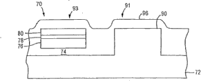
In other example of the present invention, soi structure 70 has the substrate 72 that comprises the silicon with first crystal orientation, and insulation BOX layer 74 and comprise the silicon layer 76 of the silicon with second crystal orientation is illustrated as Figure 15.Knownly comprise that the SOI wafer that has a silicon layer of different crystal orientations with silicon substrate is the crystallographic orientation wafer.In some example of the present invention, soi structure 70 comprises having<silicon layer 76 of 100〉crystal orientation silicon substrate 72 and having<110〉crystal orientation.In some other example of the present invention, substrate 72 comprises having<110〉crystal orientation silicon, and silicon layer 76 comprises having<100〉crystal orientation silicon.The substrate that mixes can be prepared via the wafer combination technology, wherein have<100〉crystal orientation first silicon substrate is incorporated into to have<110〉crystal orientation silicon substrate.In some example of the present invention, silicon layer 76 is formed up to about 30nm and is about 200nm about 300nm extremely to the thickness of the thickness of about 100nm and BOX layer 74.
The present invention is not limited to have different crystal orientations wherein and is<100〉and<110〉crystal orientation different crystal orientations silicon layer.Being familiar with this technology personage can be clear, the present invention can be applicable to any two kinds of silicon wafers to, comprise<111〉and<311〉crystal orientation.In addition, with any above-mentioned crystal face that is orientated to angle all within the scope of the present invention.
As shown in figure 16, as before, then on silicon layer 76, form oxide skin(coating) 78 and silicon nitride layer 80.As shown in figure 17, in soi structure 70, form the upper surface 84 of perforate 82 to expose silicon substrate 72.As before, perforate 82 is formed by known photoetching and etching technique.
As shown in figure 18, deposition second silicon nitride layer 86 on soi structure 70.Then anisotropically etching second silicon nitride layer 86 in perforate 82, to form side wall spacer 88.Then make it in perforate 80, extend at growth selectivity silicon epitaxial layers 90 on the top of silicon substrate 72.Silicon epitaxial layers 90 has identical crystal orientation with silicon substrate 72.Then use the CMP technology to make soi structure 70 complanations, make upper surface 92 copline substantially of the silicon epitaxial layers 90 and second silicon nitride layer 80, as shown in figure 21.
As shown in figure 22, in soi structure 70, form groove 94 to expose surface 95 on the silicon substrate 72 to the open air.Form the first area 91 and second area 93 of groove 94 to isolate soi structure 70.Form groove 94 and then filled with the appropriate insulation material, as before illustrated according to known STI technology.Configuration trench 94 forms groove 94 simultaneously to remove side wall spacer 88.Then,, illustrated as Figure 23 as Si oxide filling groove 94 with appropriate insulation material 96.Then use the CMP technology to make silicon layer 96 complanations of deposition, as discussed previously again as, remove second silicon nitride layer 80 and oxide skin(coating) 78 by using suitable etchant, with the structure 70 that complanation is provided, as shown in figure 24.
As discussed previously, with in oxonium ion 98 implant infrastructures 70 to form insulation BOX layer 100, shown in Figure 25 A.In other example of the present invention, silica or silicon nitride hard mask 102 protection second area 93 during oxonium ion 98 is implanted first area 91 does not suffer damage.Then make structure 70 thermal annealings.The result of SIMOX processing procedure, the resulting structures 70 of Figure 25 A and 25B comprises first area 91 and the second area 93 with silicon-on-insulator configuration, wherein first area 91 and second area 93 comprise the silicon with different crystal orientations.In some example of the present invention, the thickness of 91 times insulating barrier 100 is less than the thickness at the insulating barrier 74 of second area 93 times in the first area.
Then form and comprise a plurality of structures 70 with the SOI MOSFET in Different Silicon crystal orientation.Illustrated as Figure 26, in the first area 91 that comprises silicon layer 90 and comprise on the second area 93 with second crystal orientation silicon and to form gate electrode 106 and gate oxide level 104 with first crystal orientation.In source electrode and drain region 107, form source electrode and drain electrode extension 108 and in channel region 115, optionally form ring-type implant 110 by ion embedding technology.The limiting voltage of first and second MOSFET 112,114 can be changed by adjusting ring-type implant dosage.
As shown in figure 27, by the deposition as the insulating material of silica or silicon nitride and follow-up anisotropic etching on structure 70 on gate electrode 106 formation gate lateral wall clearance wall 116.Be implanted in formation severe doped region 111 in source electrode and the drain region 107 by known techniques such as ion.As discussed previously, form PMOSFET in source electrode and the drain region 107 and form NMOSFET by N-type dopant is implanted in source electrode and the drain region 107 by P-type dopant is implanted.Since the PMOSFET performance can by have<make PMOSFET on 110〉crystal orientation the silicon and promote widely, so make comprise<silicon layer of 110〉crystal orientation silicon mixes with P-type dopant in source electrode and drain region 107.Mix with N-type dopant comprise<silicon layer of 100〉crystal orientation silicon to be to form NMOSFET.
Follow depositing metal layers on structure 70.With metal level heating so that metal level with in source electrode and drain region 107 and gate electrode 106 under square pasc reaction to form metal silicide contact 120,122 in source electrode and drain region 107 and on the gate electrode 106, as shown in figure 28.
In some example of the present invention, be that a kind of silicon substrate 132 that comprises first crystal orientation, BOX layer 134, and the soi structure 130 of the silicon layer 136 in second crystal orientation are provided, illustrated as Figure 29.Soi structure 130 is processed the part depletion MOSFET 138 that comprises the silicon layer 146 with first crystal orientation to provide according to the described step of Fig. 2 to 14, and have second crystal orientation 148 on BOX layer 142 silicon layer 136 exhaust MOSFET 140 fully.In other example of the present invention, BOX layer 142 does not extend not exhausting fully under the MOSFET 140, as about the person of stating before Figure 11 B.
The example system that this specification disclosed only is the purpose of explanation, should not be illustrated as the limitation scope of patent protection.Being familiar with this technology personage can be clear, and the revealer of this specification institute is contained example miscellaneous but not only is this paper certain illustrated person.
Claims (10)
1. a method that forms semiconductor device comprises the following steps:
Silicon on insulated substrate is provided, and this silicon on insulated substrate comprises substrate (12), silicon layer (16) on this substrate (12) and first insulating barrier (14) be inserted in therebetween;
In the first area of this silicon on insulated substrate, form perforate (22) by a part that removes this silicon layer (16) and this first insulating barrier (14), with a part (24) that exposes this substrate layer;
Grows epitaxial silicon (30) optionally in this perforate (22); And
Form second insulating barrier (40) in this silicon (30) in growing in the perforate of this first area (22), with in this perforate (22) growth silicon (30) and this substrate (12) between insulating barrier (40) is provided, wherein this structure comprises the second area that separates with this first area, the silicon (30) that second insulating barrier (40) is gone up growth in this first area comprise silicon with first crystal orientation and in this second area the silicon layer (16) on first insulating barrier (14) comprise silicon with second crystal orientation.
2. the method for formation semiconductor device as claimed in claim 1, wherein the thickness of this second insulating barrier (40) in this first area is less than the thickness of this first insulating barrier (14) in the second area of this structure.
3. the method for formation semiconductor device as claimed in claim 2 further is included in this first area to form part depletion MOSFET (54) and to form in this second area and exhausts MOSFET (52) fully.
4. the method for formation semiconductor device as claimed in claim 3, the silicon (30) that further is included in this silicon layer (16) on this first insulating barrier (14) and this growth on this second insulating barrier (40) is gone up source electrode and drain region (60) that form protuberance.
5. the method for formation semiconductor device as claimed in claim 4 further is included in and forms silicide contacts (64) in the source electrode of this protuberance and drain region (60).
6. the method for formation semiconductor device as claimed in claim 3 further is included in and forms ring-type infusion (50) among this part depletion MOSFET (54).
7. the method for formation semiconductor device as claimed in claim 1 further is included in and forms insulative sidewall clearance wall (28) on the sidewall of this perforate (22).
8. the method for formation semiconductor device as claimed in claim 1 further comprises:
In this silicon on insulated substrate, form groove (34); And
Fill this groove (34) with insulating material (36), to isolate this first area and this second area.
9. the method for formation semiconductor device as claimed in claim 1, wherein this silicon with first crystal orientation have<100〉crystal orientation and this silicon with second crystal orientation have<110〉crystal orientation.
10. the method for formation semiconductor device as claimed in claim 9 further is included in this first area and forms NMOSFET and form PMOSFET in this second area.
Applications Claiming Priority (2)
| Application Number | Priority Date | Filing Date | Title |
|---|---|---|---|
| US10/976,780 | 2004-11-01 | ||
| US10/976,780 US7235433B2 (en) | 2004-11-01 | 2004-11-01 | Silicon-on-insulator semiconductor device with silicon layers having different crystal orientations and method of forming the silicon-on-insulator semiconductor device |
Publications (2)
| Publication Number | Publication Date |
|---|---|
| CN101044621A CN101044621A (en) | 2007-09-26 |
| CN100477235C true CN100477235C (en) | 2009-04-08 |
Family
ID=36074339
Family Applications (1)
| Application Number | Title | Priority Date | Filing Date |
|---|---|---|---|
| CNB2005800358985A Active CN100477235C (en) | 2004-11-01 | 2005-10-12 | Method for forming semiconductor device |
Country Status (7)
| Country | Link |
|---|---|
| US (1) | US7235433B2 (en) |
| EP (1) | EP1815520B1 (en) |
| JP (1) | JP5039557B2 (en) |
| KR (1) | KR101124657B1 (en) |
| CN (1) | CN100477235C (en) |
| TW (1) | TWI382492B (en) |
| WO (1) | WO2006049833A1 (en) |
Families Citing this family (22)
| Publication number | Priority date | Publication date | Assignee | Title |
|---|---|---|---|---|
| US7253034B2 (en) * | 2004-07-29 | 2007-08-07 | International Business Machines Corporation | Dual SIMOX hybrid orientation technology (HOT) substrates |
| US7851916B2 (en) * | 2005-03-17 | 2010-12-14 | Taiwan Semiconductor Manufacturing Co., Ltd. | Strain silicon wafer with a crystal orientation (100) in flip chip BGA package |
| US7432149B2 (en) * | 2005-06-23 | 2008-10-07 | Taiwan Semiconductor Manufacturing Company, Ltd. | CMOS on SOI substrates with hybrid crystal orientations |
| US7611937B2 (en) * | 2005-06-24 | 2009-11-03 | Taiwan Semiconductor Manufacturing Company, Ltd. | High performance transistors with hybrid crystal orientations |
| US7737532B2 (en) * | 2005-09-06 | 2010-06-15 | Taiwan Semiconductor Manufacturing Company, Ltd. | Hybrid Schottky source-drain CMOS for high mobility and low barrier |
| US7396407B2 (en) * | 2006-04-18 | 2008-07-08 | International Business Machines Corporation | Trench-edge-defect-free recrystallization by edge-angle-optimized solid phase epitaxy: method and applications to hybrid orientation substrates |
| US7452784B2 (en) * | 2006-05-25 | 2008-11-18 | International Business Machines Corporation | Formation of improved SOI substrates using bulk semiconductor wafers |
| KR101377348B1 (en) * | 2006-07-13 | 2014-03-25 | 고에키자이단호진 고쿠사이카가쿠 신고우자이단 | semiconductor device |
| FR2905519B1 (en) * | 2006-08-31 | 2008-12-19 | St Microelectronics Sa | PROCESS FOR MANUFACTURING INTEGRATED CIRCUIT WITH COMPLETELY DEPLETED AND PARTIALLY DEPLETED TRANSISTORS |
| FR2915318B1 (en) * | 2007-04-20 | 2009-07-17 | St Microelectronics Crolles 2 | METHOD OF MAKING AN ELECTRONIC CIRCUIT INTEGRATED WITH TWO PORTIONS OF ACTIVE LAYERS HAVING DIFFERENT CRYSTALLINE ORIENTATIONS |
| EP1993130A3 (en) * | 2007-05-17 | 2011-09-07 | Semiconductor Energy Laboratory Co., Ltd. | Semiconductor device and method for manufacturing the same |
| JP2009072845A (en) * | 2007-09-19 | 2009-04-09 | Oki Semiconductor Co Ltd | Method for manufacturing semiconductor device |
| JP5394043B2 (en) * | 2007-11-19 | 2014-01-22 | 株式会社半導体エネルギー研究所 | Semiconductor substrate, semiconductor device using the same, and manufacturing method thereof |
| US8039401B2 (en) * | 2007-12-14 | 2011-10-18 | Fairchild Semiconductor Corporation | Structure and method for forming hybrid substrate |
| US7956415B2 (en) * | 2008-06-05 | 2011-06-07 | International Business Machines Corporation | SOI transistor having a carrier recombination structure in a body |
| US8193616B2 (en) * | 2009-06-29 | 2012-06-05 | Kabushiki Kaisha Toshiba | Semiconductor device on direct silicon bonded substrate with different layer thickness |
| CN102790004B (en) * | 2011-05-16 | 2014-06-11 | 中国科学院上海微系统与信息技术研究所 | Preparation method of full-isolation mixed crystal orientation crystal orientation silicon-on-insulator (SOI) |
| JP6997501B2 (en) * | 2017-03-24 | 2022-01-17 | 旭化成エレクトロニクス株式会社 | Semiconductor devices and methods for manufacturing semiconductor devices |
| US10748934B2 (en) * | 2018-08-28 | 2020-08-18 | Qualcomm Incorporated | Silicon on insulator with multiple semiconductor thicknesses using layer transfer |
| CN111009530A (en) * | 2018-10-08 | 2020-04-14 | 世界先进积体电路股份有限公司 | Semiconductor structure and manufacturing method |
| US11348944B2 (en) * | 2020-04-17 | 2022-05-31 | Taiwan Semiconductor Manufacturing Company Limited | Semiconductor wafer with devices having different top layer thicknesses |
| US12074024B2 (en) | 2021-12-29 | 2024-08-27 | Taiwan Semiconductor Manufacturing Company, Ltd. | Semiconductor devices and methods of manufacturing thereof |
Family Cites Families (25)
| Publication number | Priority date | Publication date | Assignee | Title |
|---|---|---|---|---|
| JPS60154548A (en) | 1984-01-24 | 1985-08-14 | Fujitsu Ltd | Manufacture of semiconductor device |
| JPH01162376A (en) | 1987-12-18 | 1989-06-26 | Fujitsu Ltd | Manufacture of semiconductor device |
| US6063677A (en) * | 1996-10-28 | 2000-05-16 | Texas Instruments Incorporated | Method of forming a MOSFET using a disposable gate and raised source and drain |
| US5894152A (en) * | 1997-06-18 | 1999-04-13 | International Business Machines Corporation | SOI/bulk hybrid substrate and method of forming the same |
| JP3265569B2 (en) | 1998-04-15 | 2002-03-11 | 日本電気株式会社 | Semiconductor device and manufacturing method thereof |
| KR100282523B1 (en) * | 1998-11-04 | 2001-02-15 | 김영환 | SOHI semiconductor device with improved electrostatic discharge protection and manufacturing method |
| US6214694B1 (en) * | 1998-11-17 | 2001-04-10 | International Business Machines Corporation | Process of making densely patterned silicon-on-insulator (SOI) region on a wafer |
| US6476445B1 (en) * | 1999-04-30 | 2002-11-05 | International Business Machines Corporation | Method and structures for dual depth oxygen layers in silicon-on-insulator processes |
| US6326247B1 (en) | 2000-06-09 | 2001-12-04 | Advanced Micro Devices, Inc. | Method of creating selectively thin silicon/oxide for making fully and partially depleted SOI on same waffer |
| US6492209B1 (en) | 2000-06-30 | 2002-12-10 | Advanced Micro Devices, Inc. | Selectively thin silicon film for creating fully and partially depleted SOI on same wafer |
| US6537891B1 (en) | 2000-08-29 | 2003-03-25 | Micron Technology, Inc. | Silicon on insulator DRAM process utilizing both fully and partially depleted devices |
| US6414355B1 (en) | 2001-01-26 | 2002-07-02 | Advanced Micro Devices, Inc. | Silicon-on-insulator (SOI) chip having an active layer of non-uniform thickness |
| US6558994B2 (en) | 2001-03-01 | 2003-05-06 | Chartered Semiconductors Maufacturing Ltd. | Dual silicon-on-insulator device wafer die |
| US6664146B1 (en) * | 2001-06-01 | 2003-12-16 | Advanced Micro Devices, Inc. | Integration of fully depleted and partially depleted field effect transistors formed in SOI technology |
| JP4322453B2 (en) * | 2001-09-27 | 2009-09-02 | 株式会社東芝 | Semiconductor device and manufacturing method thereof |
| JP3825688B2 (en) * | 2001-12-25 | 2006-09-27 | 株式会社東芝 | Manufacturing method of semiconductor device |
| JP3943932B2 (en) * | 2001-12-27 | 2007-07-11 | 株式会社東芝 | Manufacturing method of semiconductor device |
| US6677646B2 (en) * | 2002-04-05 | 2004-01-13 | International Business Machines Corporation | Method and structure of a disposable reversed spacer process for high performance recessed channel CMOS |
| US6828630B2 (en) * | 2003-01-07 | 2004-12-07 | International Business Machines Corporation | CMOS device on ultrathin SOI with a deposited raised source/drain, and a method of manufacture |
| US6902962B2 (en) | 2003-04-04 | 2005-06-07 | Taiwan Semiconductor Manufacturing Company, Ltd. | Silicon-on-insulator chip with multiple crystal orientations |
| US6830962B1 (en) * | 2003-08-05 | 2004-12-14 | International Business Machines Corporation | Self-aligned SOI with different crystal orientation using wafer bonding and SIMOX processes |
| US20050116290A1 (en) | 2003-12-02 | 2005-06-02 | De Souza Joel P. | Planar substrate with selected semiconductor crystal orientations formed by localized amorphization and recrystallization of stacked template layers |
| US6949420B1 (en) * | 2004-03-12 | 2005-09-27 | Sony Corporation | Silicon-on-insulator (SOI) substrate having dual surface crystallographic orientations and method of forming same |
| US7291886B2 (en) | 2004-06-21 | 2007-11-06 | International Business Machines Corporation | Hybrid substrate technology for high-mobility planar and multiple-gate MOSFETs |
| JP2006040911A (en) * | 2004-07-22 | 2006-02-09 | Renesas Technology Corp | Semiconductor device and its manufacturing method |
-
2004
- 2004-11-01 US US10/976,780 patent/US7235433B2/en not_active Expired - Fee Related
-
2005
- 2005-10-12 JP JP2007538966A patent/JP5039557B2/en active Active
- 2005-10-12 KR KR1020077009978A patent/KR101124657B1/en not_active IP Right Cessation
- 2005-10-12 WO PCT/US2005/036777 patent/WO2006049833A1/en active Application Filing
- 2005-10-12 EP EP05812444A patent/EP1815520B1/en active Active
- 2005-10-12 CN CNB2005800358985A patent/CN100477235C/en active Active
- 2005-10-24 TW TW094137085A patent/TWI382492B/en active
Also Published As
| Publication number | Publication date |
|---|---|
| WO2006049833A1 (en) | 2006-05-11 |
| TWI382492B (en) | 2013-01-11 |
| KR101124657B1 (en) | 2012-04-19 |
| JP5039557B2 (en) | 2012-10-03 |
| JP2008518475A (en) | 2008-05-29 |
| US7235433B2 (en) | 2007-06-26 |
| CN101044621A (en) | 2007-09-26 |
| KR20070065902A (en) | 2007-06-25 |
| TW200620537A (en) | 2006-06-16 |
| EP1815520B1 (en) | 2012-05-02 |
| US20060091427A1 (en) | 2006-05-04 |
| EP1815520A1 (en) | 2007-08-08 |
Similar Documents
| Publication | Publication Date | Title |
|---|---|---|
| CN100477235C (en) | Method for forming semiconductor device | |
| CN100578751C (en) | Semiconductor device and method of making semiconductor device comprising multiple stacked hybrid orientation layers | |
| US6664598B1 (en) | Polysilicon back-gated SOI MOSFET for dynamic threshold voltage control | |
| US6432754B1 (en) | Double SOI device with recess etch and epitaxy | |
| US6707062B2 (en) | Transistor in a semiconductor device with an elevated channel and a source drain | |
| US7075150B2 (en) | Ultra-thin Si channel MOSFET using a self-aligned oxygen implant and damascene technique | |
| TW506076B (en) | CMOS integrated circuit devices and substrates having buried silicon germanium layers therein and methods of forming same | |
| US20070228473A1 (en) | ULTRA-THIN Si MOSFET DEVICE STRUCTURE AND METHOD OF MANUFACTURE | |
| US7687865B2 (en) | Method and structure to reduce contact resistance on thin silicon-on-insulator device | |
| US20070128776A1 (en) | Isolated fully depleted silicon-on-insulator regions by selective etch | |
| US6812105B1 (en) | Ultra-thin channel device with raised source and drain and solid source extension doping | |
| US20220102553A1 (en) | Damage implantation of cap layer | |
| US7514337B2 (en) | Semiconductor device using EPI-layer and method of forming the same | |
| WO2005094299A2 (en) | Improved cmos transistors and methods of forming same | |
| US6548362B1 (en) | Method of forming MOSFET with buried contact and air-gap gate structure | |
| US6495887B1 (en) | Argon implantation after silicidation for improved floating-body effects | |
| US6326272B1 (en) | Method for forming self-aligned elevated transistor | |
| US6762459B2 (en) | Method for fabricating MOS device with halo implanted region | |
| US6566680B1 (en) | Semiconductor-on-insulator (SOI) tunneling junction transistor | |
| US6657261B2 (en) | Ground-plane device with back oxide topography | |
| US6251744B1 (en) | Implant method to improve characteristics of high voltage isolation and high voltage breakdown | |
| EP0959497A1 (en) | A method of forming an ultra-thin soi electrostatic discharge protection device | |
| US20020102813A1 (en) | Method for manufacturing semiconductor device on silicon-on-insulator substrate |
Legal Events
| Date | Code | Title | Description |
|---|---|---|---|
| C06 | Publication | ||
| PB01 | Publication | ||
| C10 | Entry into substantive examination | ||
| SE01 | Entry into force of request for substantive examination | ||
| C14 | Grant of patent or utility model | ||
| GR01 | Patent grant |