CN100466885C - Multilayer circuit board forming method and multilayer circuit board - Google Patents
Multilayer circuit board forming method and multilayer circuit board Download PDFInfo
- Publication number
- CN100466885C CN100466885C CNB031458092A CN03145809A CN100466885C CN 100466885 C CN100466885 C CN 100466885C CN B031458092 A CNB031458092 A CN B031458092A CN 03145809 A CN03145809 A CN 03145809A CN 100466885 C CN100466885 C CN 100466885C
- Authority
- CN
- China
- Prior art keywords
- circuit board
- circuit
- conductor
- multilayer circuit
- mask
- Prior art date
- Legal status (The legal status is an assumption and is not a legal conclusion. Google has not performed a legal analysis and makes no representation as to the accuracy of the status listed.)
- Expired - Fee Related
Links
- 238000000034 method Methods 0.000 title claims abstract description 180
- 239000004020 conductor Substances 0.000 claims abstract description 98
- 239000011810 insulating material Substances 0.000 claims abstract description 32
- 238000009413 insulation Methods 0.000 claims description 52
- 230000015572 biosynthetic process Effects 0.000 claims description 47
- 230000004888 barrier function Effects 0.000 claims description 38
- 238000007639 printing Methods 0.000 claims description 27
- 239000011347 resin Substances 0.000 claims description 24
- 229920005989 resin Polymers 0.000 claims description 24
- 238000010438 heat treatment Methods 0.000 claims description 22
- 238000013517 stratification Methods 0.000 claims description 16
- 239000012774 insulation material Substances 0.000 claims description 12
- RYGMFSIKBFXOCR-UHFFFAOYSA-N Copper Chemical compound [Cu] RYGMFSIKBFXOCR-UHFFFAOYSA-N 0.000 claims description 10
- PXHVJJICTQNCMI-UHFFFAOYSA-N Nickel Chemical compound [Ni] PXHVJJICTQNCMI-UHFFFAOYSA-N 0.000 claims description 8
- KDLHZDBZIXYQEI-UHFFFAOYSA-N Palladium Chemical compound [Pd] KDLHZDBZIXYQEI-UHFFFAOYSA-N 0.000 claims description 8
- 239000011248 coating agent Substances 0.000 claims description 7
- 150000001875 compounds Chemical class 0.000 claims description 7
- 229910052751 metal Inorganic materials 0.000 claims description 7
- 239000002184 metal Substances 0.000 claims description 7
- 238000000576 coating method Methods 0.000 claims description 5
- BQCADISMDOOEFD-UHFFFAOYSA-N Silver Chemical compound [Ag] BQCADISMDOOEFD-UHFFFAOYSA-N 0.000 claims description 4
- ATJFFYVFTNAWJD-UHFFFAOYSA-N Tin Chemical compound [Sn] ATJFFYVFTNAWJD-UHFFFAOYSA-N 0.000 claims description 4
- 229910052802 copper Inorganic materials 0.000 claims description 4
- 239000010949 copper Substances 0.000 claims description 4
- 230000007797 corrosion Effects 0.000 claims description 4
- 238000005260 corrosion Methods 0.000 claims description 4
- PCHJSUWPFVWCPO-UHFFFAOYSA-N gold Chemical compound [Au] PCHJSUWPFVWCPO-UHFFFAOYSA-N 0.000 claims description 4
- 229910052737 gold Inorganic materials 0.000 claims description 4
- 239000010931 gold Substances 0.000 claims description 4
- 229910052759 nickel Inorganic materials 0.000 claims description 4
- 229910052763 palladium Inorganic materials 0.000 claims description 4
- 239000004033 plastic Substances 0.000 claims description 4
- 229920003023 plastic Polymers 0.000 claims description 4
- 229910052709 silver Inorganic materials 0.000 claims description 4
- 239000004332 silver Substances 0.000 claims description 4
- 229910052718 tin Inorganic materials 0.000 claims description 4
- 239000000956 alloy Substances 0.000 claims description 3
- 229910045601 alloy Inorganic materials 0.000 claims description 3
- 238000004821 distillation Methods 0.000 claims description 3
- 239000004925 Acrylic resin Substances 0.000 claims description 2
- 229920000178 Acrylic resin Polymers 0.000 claims description 2
- 239000004677 Nylon Substances 0.000 claims description 2
- 239000000203 mixture Substances 0.000 claims description 2
- 229920001778 nylon Polymers 0.000 claims description 2
- 238000001020 plasma etching Methods 0.000 claims description 2
- 229920000915 polyvinyl chloride Polymers 0.000 claims description 2
- 239000000126 substance Substances 0.000 claims description 2
- 239000005749 Copper compound Substances 0.000 claims 1
- BZHJMEDXRYGGRV-UHFFFAOYSA-N Vinyl chloride Chemical compound ClC=C BZHJMEDXRYGGRV-UHFFFAOYSA-N 0.000 claims 1
- 239000002253 acid Substances 0.000 claims 1
- 150000001880 copper compounds Chemical class 0.000 claims 1
- 150000002344 gold compounds Chemical class 0.000 claims 1
- 150000002736 metal compounds Chemical class 0.000 claims 1
- 239000000178 monomer Substances 0.000 claims 1
- 150000002816 nickel compounds Chemical class 0.000 claims 1
- 150000002894 organic compounds Chemical class 0.000 claims 1
- 150000002941 palladium compounds Chemical class 0.000 claims 1
- 229940100890 silver compound Drugs 0.000 claims 1
- 150000003379 silver compounds Chemical class 0.000 claims 1
- 239000007921 spray Substances 0.000 claims 1
- 150000003606 tin compounds Chemical class 0.000 claims 1
- 230000000873 masking effect Effects 0.000 abstract 1
- 239000010410 layer Substances 0.000 description 35
- 239000004065 semiconductor Substances 0.000 description 15
- 239000013256 coordination polymer Substances 0.000 description 14
- 239000000463 material Substances 0.000 description 12
- 239000010408 film Substances 0.000 description 10
- KRHYYFGTRYWZRS-UHFFFAOYSA-M Fluoride anion Chemical compound [F-] KRHYYFGTRYWZRS-UHFFFAOYSA-M 0.000 description 6
- 239000011889 copper foil Substances 0.000 description 6
- 238000010586 diagram Methods 0.000 description 6
- 238000007650 screen-printing Methods 0.000 description 6
- 239000002245 particle Substances 0.000 description 5
- 239000000843 powder Substances 0.000 description 5
- 229920002799 BoPET Polymers 0.000 description 4
- 239000005041 Mylar™ Substances 0.000 description 4
- 238000001035 drying Methods 0.000 description 4
- 239000003822 epoxy resin Substances 0.000 description 4
- 229920000647 polyepoxide Polymers 0.000 description 4
- 238000012545 processing Methods 0.000 description 4
- 238000011049 filling Methods 0.000 description 3
- 238000003754 machining Methods 0.000 description 3
- 238000012546 transfer Methods 0.000 description 3
- UFWIBTONFRDIAS-UHFFFAOYSA-N Naphthalene Chemical compound C1=CC=CC2=CC=CC=C21 UFWIBTONFRDIAS-UHFFFAOYSA-N 0.000 description 2
- WNLRTRBMVRJNCN-UHFFFAOYSA-N adipic acid Chemical compound OC(=O)CCCCC(O)=O WNLRTRBMVRJNCN-UHFFFAOYSA-N 0.000 description 2
- 239000002585 base Substances 0.000 description 2
- 239000003795 chemical substances by application Substances 0.000 description 2
- 238000007796 conventional method Methods 0.000 description 2
- 229920001721 polyimide Polymers 0.000 description 2
- 239000009719 polyimide resin Substances 0.000 description 2
- KDYFGRWQOYBRFD-UHFFFAOYSA-N succinic acid Chemical compound OC(=O)CCC(O)=O KDYFGRWQOYBRFD-UHFFFAOYSA-N 0.000 description 2
- 229920001169 thermoplastic Polymers 0.000 description 2
- 239000004416 thermosoftening plastic Substances 0.000 description 2
- NSGXIBWMJZWTPY-UHFFFAOYSA-N 1,1,1,3,3,3-hexafluoropropane Chemical compound FC(F)(F)CC(F)(F)F NSGXIBWMJZWTPY-UHFFFAOYSA-N 0.000 description 1
- NIXOWILDQLNWCW-UHFFFAOYSA-M Acrylate Chemical compound [O-]C(=O)C=C NIXOWILDQLNWCW-UHFFFAOYSA-M 0.000 description 1
- LFQSCWFLJHTTHZ-UHFFFAOYSA-N EtOH Substances CCO LFQSCWFLJHTTHZ-UHFFFAOYSA-N 0.000 description 1
- 150000001252 acrylic acid derivatives Chemical class 0.000 description 1
- 239000000853 adhesive Substances 0.000 description 1
- 230000001070 adhesive effect Effects 0.000 description 1
- 235000011037 adipic acid Nutrition 0.000 description 1
- 239000001361 adipic acid Substances 0.000 description 1
- 239000003513 alkali Substances 0.000 description 1
- 238000013459 approach Methods 0.000 description 1
- 239000003990 capacitor Substances 0.000 description 1
- 238000002485 combustion reaction Methods 0.000 description 1
- 239000000039 congener Substances 0.000 description 1
- 238000001816 cooling Methods 0.000 description 1
- 230000000994 depressogenic effect Effects 0.000 description 1
- 238000013461 design Methods 0.000 description 1
- 230000005611 electricity Effects 0.000 description 1
- 230000008030 elimination Effects 0.000 description 1
- 238000003379 elimination reaction Methods 0.000 description 1
- 238000005516 engineering process Methods 0.000 description 1
- 230000002349 favourable effect Effects 0.000 description 1
- 239000012530 fluid Substances 0.000 description 1
- 239000003292 glue Substances 0.000 description 1
- 238000000227 grinding Methods 0.000 description 1
- 238000002347 injection Methods 0.000 description 1
- 239000007924 injection Substances 0.000 description 1
- 239000012212 insulator Substances 0.000 description 1
- 239000011229 interlayer Substances 0.000 description 1
- 230000001788 irregular Effects 0.000 description 1
- 238000003475 lamination Methods 0.000 description 1
- 239000003094 microcapsule Substances 0.000 description 1
- 238000012986 modification Methods 0.000 description 1
- 230000004048 modification Effects 0.000 description 1
- -1 perfluoroalkyl ethanol Chemical compound 0.000 description 1
- 238000005498 polishing Methods 0.000 description 1
- 238000002360 preparation method Methods 0.000 description 1
- 238000003825 pressing Methods 0.000 description 1
- 239000000243 solution Substances 0.000 description 1
- 239000002904 solvent Substances 0.000 description 1
- 229960005137 succinic acid Drugs 0.000 description 1
- 239000010409 thin film Substances 0.000 description 1
- 239000011135 tin Substances 0.000 description 1
- 238000003466 welding Methods 0.000 description 1
Images


Classifications
-
- H—ELECTRICITY
- H05—ELECTRIC TECHNIQUES NOT OTHERWISE PROVIDED FOR
- H05K—PRINTED CIRCUITS; CASINGS OR CONSTRUCTIONAL DETAILS OF ELECTRIC APPARATUS; MANUFACTURE OF ASSEMBLAGES OF ELECTRICAL COMPONENTS
- H05K3/00—Apparatus or processes for manufacturing printed circuits
- H05K3/46—Manufacturing multilayer circuits
-
- H—ELECTRICITY
- H05—ELECTRIC TECHNIQUES NOT OTHERWISE PROVIDED FOR
- H05K—PRINTED CIRCUITS; CASINGS OR CONSTRUCTIONAL DETAILS OF ELECTRIC APPARATUS; MANUFACTURE OF ASSEMBLAGES OF ELECTRICAL COMPONENTS
- H05K3/00—Apparatus or processes for manufacturing printed circuits
- H05K3/0011—Working of insulating substrates or insulating layers
- H05K3/0017—Etching of the substrate by chemical or physical means
-
- H—ELECTRICITY
- H05—ELECTRIC TECHNIQUES NOT OTHERWISE PROVIDED FOR
- H05K—PRINTED CIRCUITS; CASINGS OR CONSTRUCTIONAL DETAILS OF ELECTRIC APPARATUS; MANUFACTURE OF ASSEMBLAGES OF ELECTRICAL COMPONENTS
- H05K2201/00—Indexing scheme relating to printed circuits covered by H05K1/00
- H05K2201/01—Dielectrics
- H05K2201/0137—Materials
- H05K2201/0179—Thin film deposited insulating layer, e.g. inorganic layer for printed capacitor
-
- H—ELECTRICITY
- H05—ELECTRIC TECHNIQUES NOT OTHERWISE PROVIDED FOR
- H05K—PRINTED CIRCUITS; CASINGS OR CONSTRUCTIONAL DETAILS OF ELECTRIC APPARATUS; MANUFACTURE OF ASSEMBLAGES OF ELECTRICAL COMPONENTS
- H05K2201/00—Indexing scheme relating to printed circuits covered by H05K1/00
- H05K2201/03—Conductive materials
- H05K2201/0332—Structure of the conductor
- H05K2201/0364—Conductor shape
- H05K2201/0376—Flush conductors, i.e. flush with the surface of the printed circuit
-
- H—ELECTRICITY
- H05—ELECTRIC TECHNIQUES NOT OTHERWISE PROVIDED FOR
- H05K—PRINTED CIRCUITS; CASINGS OR CONSTRUCTIONAL DETAILS OF ELECTRIC APPARATUS; MANUFACTURE OF ASSEMBLAGES OF ELECTRICAL COMPONENTS
- H05K2203/00—Indexing scheme relating to apparatus or processes for manufacturing printed circuits covered by H05K3/00
- H05K2203/02—Details related to mechanical or acoustic processing, e.g. drilling, punching, cutting, using ultrasound
- H05K2203/0278—Flat pressure, e.g. for connecting terminals with anisotropic conductive adhesive
-
- H—ELECTRICITY
- H05—ELECTRIC TECHNIQUES NOT OTHERWISE PROVIDED FOR
- H05K—PRINTED CIRCUITS; CASINGS OR CONSTRUCTIONAL DETAILS OF ELECTRIC APPARATUS; MANUFACTURE OF ASSEMBLAGES OF ELECTRICAL COMPONENTS
- H05K2203/00—Indexing scheme relating to apparatus or processes for manufacturing printed circuits covered by H05K3/00
- H05K2203/05—Patterning and lithography; Masks; Details of resist
- H05K2203/0562—Details of resist
- H05K2203/0582—Coating by resist, i.e. resist used as mask for application of insulating coating or of second resist
-
- H—ELECTRICITY
- H05—ELECTRIC TECHNIQUES NOT OTHERWISE PROVIDED FOR
- H05K—PRINTED CIRCUITS; CASINGS OR CONSTRUCTIONAL DETAILS OF ELECTRIC APPARATUS; MANUFACTURE OF ASSEMBLAGES OF ELECTRICAL COMPONENTS
- H05K3/00—Apparatus or processes for manufacturing printed circuits
- H05K3/0011—Working of insulating substrates or insulating layers
- H05K3/0017—Etching of the substrate by chemical or physical means
- H05K3/002—Etching of the substrate by chemical or physical means by liquid chemical etching
-
- H—ELECTRICITY
- H05—ELECTRIC TECHNIQUES NOT OTHERWISE PROVIDED FOR
- H05K—PRINTED CIRCUITS; CASINGS OR CONSTRUCTIONAL DETAILS OF ELECTRIC APPARATUS; MANUFACTURE OF ASSEMBLAGES OF ELECTRICAL COMPONENTS
- H05K3/00—Apparatus or processes for manufacturing printed circuits
- H05K3/0011—Working of insulating substrates or insulating layers
- H05K3/0017—Etching of the substrate by chemical or physical means
- H05K3/0041—Etching of the substrate by chemical or physical means by plasma etching
-
- H—ELECTRICITY
- H05—ELECTRIC TECHNIQUES NOT OTHERWISE PROVIDED FOR
- H05K—PRINTED CIRCUITS; CASINGS OR CONSTRUCTIONAL DETAILS OF ELECTRIC APPARATUS; MANUFACTURE OF ASSEMBLAGES OF ELECTRICAL COMPONENTS
- H05K3/00—Apparatus or processes for manufacturing printed circuits
- H05K3/46—Manufacturing multilayer circuits
- H05K3/4644—Manufacturing multilayer circuits by building the multilayer layer by layer, i.e. build-up multilayer circuits
-
- Y—GENERAL TAGGING OF NEW TECHNOLOGICAL DEVELOPMENTS; GENERAL TAGGING OF CROSS-SECTIONAL TECHNOLOGIES SPANNING OVER SEVERAL SECTIONS OF THE IPC; TECHNICAL SUBJECTS COVERED BY FORMER USPC CROSS-REFERENCE ART COLLECTIONS [XRACs] AND DIGESTS
- Y10—TECHNICAL SUBJECTS COVERED BY FORMER USPC
- Y10T—TECHNICAL SUBJECTS COVERED BY FORMER US CLASSIFICATION
- Y10T29/00—Metal working
- Y10T29/49—Method of mechanical manufacture
- Y10T29/49002—Electrical device making
- Y10T29/49117—Conductor or circuit manufacturing
- Y10T29/49124—On flat or curved insulated base, e.g., printed circuit, etc.
- Y10T29/49126—Assembling bases
-
- Y—GENERAL TAGGING OF NEW TECHNOLOGICAL DEVELOPMENTS; GENERAL TAGGING OF CROSS-SECTIONAL TECHNOLOGIES SPANNING OVER SEVERAL SECTIONS OF THE IPC; TECHNICAL SUBJECTS COVERED BY FORMER USPC CROSS-REFERENCE ART COLLECTIONS [XRACs] AND DIGESTS
- Y10—TECHNICAL SUBJECTS COVERED BY FORMER USPC
- Y10T—TECHNICAL SUBJECTS COVERED BY FORMER US CLASSIFICATION
- Y10T29/00—Metal working
- Y10T29/49—Method of mechanical manufacture
- Y10T29/49002—Electrical device making
- Y10T29/49117—Conductor or circuit manufacturing
- Y10T29/49124—On flat or curved insulated base, e.g., printed circuit, etc.
- Y10T29/4913—Assembling to base an electrical component, e.g., capacitor, etc.
-
- Y—GENERAL TAGGING OF NEW TECHNOLOGICAL DEVELOPMENTS; GENERAL TAGGING OF CROSS-SECTIONAL TECHNOLOGIES SPANNING OVER SEVERAL SECTIONS OF THE IPC; TECHNICAL SUBJECTS COVERED BY FORMER USPC CROSS-REFERENCE ART COLLECTIONS [XRACs] AND DIGESTS
- Y10—TECHNICAL SUBJECTS COVERED BY FORMER USPC
- Y10T—TECHNICAL SUBJECTS COVERED BY FORMER US CLASSIFICATION
- Y10T29/00—Metal working
- Y10T29/49—Method of mechanical manufacture
- Y10T29/49002—Electrical device making
- Y10T29/49117—Conductor or circuit manufacturing
- Y10T29/49124—On flat or curved insulated base, e.g., printed circuit, etc.
- Y10T29/49155—Manufacturing circuit on or in base
- Y10T29/49165—Manufacturing circuit on or in base by forming conductive walled aperture in base
Abstract
A multilayered circuit board and a method of forming the multilayer circuit board are provided. In a first circuit forming process P1p, a first circuit 12a is formed on an insulating board 11a with a conductor 12a; in a circuit embedding process P2p, the first circuit 12a is embedded in the insulating board 11a so as to have a predetermined surface flatness S and a predetermined parallelism P; in a masking process P4p, a pilot hole 15, 20 for a via hole 4, 4a is masked at a part of the surface of the circuit 12a; in an insulating layer forming process P5p, an insulating material 11b is applied as a layer to the surface except the mask 14; in an insulating material layer flattening process, the surface of the insulating material layer 11b is flattened so as to have the predetermined surface flatness S and the predetermined parallelism P; and in a pilot hole forming process, the mask 14 is removed.
Description
Technical field
The present invention relates to multilayer circuit, on every layer of electronic circuit layer, electronic component is housed all by the electronic circuit stratification is formed, and the method that forms above-mentioned multilayer circuit board.
Background technology
With reference to figure 5,6 and 7, the conventional method that is used to form multilayer circuit board is described below.Can briefly be divided into two big classes to these methods, in this paper back they be referred to as to continue formation methods and progressively form method.
In the formation method that continues, make their stratification so that be connected to each other being ready to requisite number purpose circuit board in advance, thereby form the multiplex circuit plate.
In progressively formation method, at first form a layer circuit board, and then on it, form another layer circuit board.Repeat this process and form requisite number purpose circuit board with whole stratification.
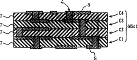
Fig. 5 and Fig. 6 illustrate an example of the above-mentioned formation method that continues.In this method, insulating material 7 is laminated together with copper foil 8, corrodes copper foil 8 then to form electronic circuit.So the circuit board that above-mentioned electronic circuit is installed on it just has been formed.Then a plurality of such circuit boards are joined to one another and have just formed multilayer circuit board.
Fig. 5 is by by 4 layer circuit board C1, the be connected to each other cross-sectional view of multilayer circuit board MSc1 of (making its stratification) structure of C2, C3 and C4.Hereinafter, circuit board C1, C2, C3 and C4 are collectively referred to as circuit board C.Every circuit board C is by thermoplastic bonding insulating material 7 and copper foil 8 laminated together formation, makes to penetrate the two aperture of insulating material 7 and copper foil 8 and form via hole 4, corrodes copper foil again and forms predetermined electronic circuit.
By by boring, laser processing, or the process of pressure processing is made aperture.Usually, these apertures are made singly by laser processing or boring.Then, the inwall of filling and applying each aperture with electric conducting material by printing process or quantitative coating machine forms via hole 4.After this manner, just distinguish all set circuit board C1, C2, C3 and C4.
Fig. 6 illustrates second layer circuit board C2 is put into process on the ground floor circuit board C1.For being put together, circuit board C1 and circuit board C2 make its stratification, can think what these circuit boards had been finished with the high accuracy size as design, think that the element of these circuit and they is placed with the high precision position relation of defined by demand, so that can not disturb each other.
Position precision in order to height is placed on accuracy to size these circuit boards C1 and the C2 that prepare with height, under predetermined temperature and pressure to those above circuit board and below heating and pressurization, thereby since the thermoplasticity and the caking property of insulating material 7 on their surface, be joined to one another.Along with such heat and pressure, the copper foil 8 that forms electronic circuit is also imbedded in the contiguous insulating material 7 except being crimped onto via hole 4, thereby has guaranteed that the electricity between these layers leads.Equally, be linked in sequence circuit board C3 and circuit board C4, thus form multilayer circuit board MSc1.
Fig. 7 illustrates a top example that progressively forms method.In this method, along with the employing of silk screen printing, piece ground of polylith circuit board forms successively.In Fig. 7, pointed out that in the graphic extension of cross section another circuit board is formed on the ground floor circuit board.In process P1, show the cross section of the completed circuit board Ca of ground floor.In process P2, laid insulating material 3 above the circuit board that in process P1, obtains as second layer circuit board Cb (not shown).In process P3, the circuit board Ca that in process 2, obtains, also the conductor 2b with second layer circuit board Cb lays.For ease of describing, on demand corresponding to process P1, the circuit board of P2 and P3 is referred to as circuit board Cc (P1) respectively, circuit board Cc (P2) and circuit board Cc (P3) in this paper back.
Circuit board Ca follows these steps to finish in process P1.At first, on the base material 1a of insulation, make an aperture, wall applies or fills with conducting material to form via hole 4a within it, secondly, the conductor 2a that is made by same conductive is printed on by predetermined pattern by silk screen printing on two faces of dielectric base material so that contact with via hole 4a, thereby is printed as the electronic circuit of ground floor.Then, make conductor 2a hardening finish circuit board Ca by drying.Here, on the base material 1a of insulation, have the part Pp that is printing conductor, on it, printing conductor 2a and do not printing conductor part Pn, on it, do not print upper conductor 2a.Formed a step Dh in a difference in height of printing conductor part Pp and do not printing between conductor part Pn, its representative is from the height of the base material 1a of insulation.
Circuit board Cc (P2) follows these steps to finish in process P2, except in process subsequently, forming the presumptive area of via hole 4a on the conductor 2a (a kind of like this zone, this paper back is called as " via hole formation part ", insulating material 3 is screen-printed to the upper surface of entire circuit plate Cc (P1), thus form will with the contacted insulating barrier L1 of second layer circuit board Cb (not shown).Reflect the uneven place that is positioned at circuit board Cc (P1) surface below the insulating barrier L1 significantly at the upper surface of the insulating barrier L1 that forms.These uneven places comprise wherein trickle a kind of be by wherein big a kind ofly then causing that conductor 2a characteristic or printed panel grid cause by printing conductor part Pp and not printing conductor part Pn.Especially, printing conductor part Pp corresponding to one group and do not printing on the partial insulative layer L1 of conductor part Pn and have big recessed/convex portion 5.This recessed/convex portion 5 comprises corresponding to the concave portion 5n that is not printing conductor part Pn with corresponding to the convex portion 5P that is printing conductor part Pp.
Circuit board Cc (P3) follows these steps to finish in process P3.In the circuit board Cc (P2) that process P2 obtains, make insulating material 3 hardening by drying after, coating or filled conductive material 2a form via hole 4a on the inwall of the part of via hole formation in the above.And, on insulating material 3, printed the conductor 2b that is used for forming second layer electronic circuit.Notice that conductor 2b is connected to ground floor conductor 2a through via hole 4a.
Conductor 2b becomes according to the uneven place on insulating barrier L1 surface the attachment state of insulating barrier 3.This is because last to the distance of the insulating material 3 that is printing conductor 2b thereon from plates for screen printing, exists difference between concave portion and convex portion.For this reason, conductor 2b is printed on the insulating material 3 in irregular mode.Therefore, the zone of designed conductor 2b is changed into designed accurate area part of generation and area part 6 (not shown) that are reduced.Also promptly, when reducing the zone and take place, partly diminish with the effective width of the circuit pattern of conductor 2b formation.And it is the equal of electrically being changed of electronic circuit that the zone of conductor 2b is changed.So the above-mentioned printed panel the earth of not stipulating degenerates the electrical characteristics of designed electronic circuit.
In order to suppress above-mentioned degenerating, the printing width of conductor 2b should be set like this, make it to consider this area part 6 that is reduced.But, this undertreatment with elimination resemble above-mentioned recessed/the significant especially above-mentioned situation that occurs in the convex portion 5.In addition, the circuit board number of plies is bigger, and the number and the size that are reduced area part 6 are bigger.Therefore, when the number of plies increases, accurately form electronic circuit and just become difficult.So, owing to be reduced area part 6, just limited the number of circuit board C that can stratification.
In the open text of the Japan Patent of the 10-No. 335787 (1998-335787), a kind of demonstration methods that is used to form circuit board has been proposed.In this method, transfer sheet is placed on the insulation board that comprises organic resin, in this thin slice, there is the skim metal to be directly bonded to resin film, then, for thin metal layer being transferred to this insulation board, peel off this resin film, thereby on the insulation board surface, formed the circuit of metal wire.
In the above-mentioned formation method that continues, circuit board together to be connected must be ready to respectively in advance with high-precision size.Equally, these circuit boards must have high-precision position to link together, and make all circuit and all elements can not disturb with other circuit and element.Consider this two classes accuracy, if controlling dimension and locational deviation inadequately, so when the number of circuit board to be connected increases, these deviations can be accumulated, thereby limited the number of circuit board lamination inexpediently, and,, can make the connection procedure that can not finish itself at worst.
Even these deviations on accuracy are suitably controlled, if but the position relation between circuit board has had variation by heating and pressure process, and so above-mentioned those troubles also can take place.In heating and pressure process, all circuit boards of stratification are heated simultaneously, cause the softening and distortion of insulating material.This tends to cause in the locational deviation of each interlayer.For this reason, also must be in heating and pressure process the accuracy of control position.And, for the operation of the making aperture of preparing via hole will be changed some times and plurality of processes, thereby, required increase of crossing number of passes in this method, caused.
On the other hand, in above-mentioned progressively formation method, on the circuit board that forms in advance, have the element that is printed on another circuit board above it and their Connection Element.Therefore, can not occur in the formation method that continues such as between circuit board about locational high accuracy and to increase number of passes so that make above-mentioned all problems of the aperture be used to prepare via hole.But, on conductor above-mentioned recessed/appearance that the protuberance place is reduced area part is significant especially.And board layer the more is reduced the number of area part and size also the more.For this reason, when the number of plies increases, form as designed electronic circuit and become difficulty.Therefore, owing to be reduced area part, circuit number that can stratification is restricted.Have, it is difficult eliminating the area part that is reduced that is caused by conductor printing again, and in other words, no matter the printing width of each conductor is how to set, so that can consider this appearance that is reduced area part, but always have a restriction.Therefore, accurately the formation of circuit is difficult, and same, and a restriction is arranged on the number of plies.
In the above-mentioned formation method that continues, conductor is to form in advance according to predetermined size and dimension.Therefore, can not occur as the area part that is reduced that in progressively formation method, occurs.But, in the formation method that continues, a plurality of circuit boards soften the insulating material of circuit board by heating and pressurization, thereby the conductor embedding also is connected with these circuit simultaneously.Therefore, in connection procedure, can not directly control the temperature and pressure that is added in insulating material and conductor.Therefore, all can not control insulating material and conductor in accuracy locational and dimensionally.Also have, also all can not control the multilayer circuit board formed by insulating material and conductor on the position and accuracy dimensionally.
If adopting transfer sheet for forming the said method of circuit board.Be applied in the continuous formation method, then control is expected to make moderate progress to accuracy to size, but can not look to making moderate progress to the position precision control of a plurality of circuit boards.And, even the transfer sheet method can be applied to progressively form method, still can not solve the problem that is reduced area part.Therefore, solve by conventional method above-mentioned, as to form multilayer circuit board the various shortcomings that cause of exclusive problem be impossible.
Summary of the invention
The intent of the present invention is to solve top all shortcomings.An object of the present invention is to provide and have highly accurately and the multilayer circuit board of quality and the method that forms above-mentioned multilayer circuit board.In this multilayer circuit board, can easily control and the mutually accuracy to size of all circuit boards of stratification and the position precision between them.Equally, also can solve the rough place of each circuit board surface.
In order to reach purpose above-mentioned, the present invention is a target with the method that forms multilayer circuit board, comprise: the first circuit forming process that forms first circuit, conductor on first flat surfaces of the smooth insulation board that this first circuit is made by insulating material on a predetermined pattern is made, and this insulation board also has second flat surfaces parallel with first flat surfaces; First circuit is embedded the first circuit telescopiny of first insulation board, and like this, the first surface and first circuit have predetermined surface flatness and first surface has the predetermined depth of parallelism with respect to second flat surfaces; On the part surface that embeds first circuit, be formed for forming the mask forming process of the mask of location hole into via hole; By insulating material is applied to the insulating barrier forming process that first flat surfaces forms insulation material layer as thin layer, this first flat surfaces has formation mask in the above except having the part surface that mask is set; Leveling insulating material laminar surface makes the insulating material laminar surface have the plane surface flatness and with respect to the insulation material layer flattening course of the depth of parallelism of second flat surfaces; And by from first circuit along with insulation material layer is removed the location hole forming process that mask forms location hole by leveling.
When with accompanying drawing one time-out, from the following detailed description of the present invention, can be to these and other objects of the present invention, characteristic, situation and advantage will become more clear.
The accompanying drawing summary
Fig. 1 illustrates the schematic diagram that forms the multilayer circuit board process according to first embodiment of the invention;
Fig. 2 is the cross-sectional view according to the second embodiment of the invention multilayer circuit board;
Fig. 3 is the schematic diagram that the formation multilayer circuit board process that is shown in Fig. 2 is shown;
Fig. 4 illustrates the schematic diagram that forms the multilayer circuit board process according to third embodiment of the invention;
Fig. 5 is the cross-sectional view of conventional multilayer circuit board;
Fig. 6 is the schematic diagram that the formation multilayer circuit board process that is shown in Fig. 5 is shown;
Fig. 7 illustrates the schematic diagram that forms a conventional multilayer circuit board process.
Embodiment
Before all embodiment describe specially to the present invention, basic conception of the present invention is described at first below.The present invention except to improve will the position and accuracy to size of all circuit boards of stratification, also to prevent the area part that in the progressively formation method of above-mentioned employing silk screen printing, occurs being reduced.
Briefly, further developed and in routine continues the formation method, be used for the preprepared circuit board is heated and pressurizes and conductor embedding insulating material, and contacted there process and the further consequential process of utilizing another conductor that in progressively formation method, lays next piece circuit board.Different with the routine formation method that continues, method of the present invention can solve a problem, this problem is owing to be required heating and the pressure process of circuit board, the accuracy that will directly control conductor and insulating material position and size is impossible, thereby, make that conversely the above-mentioned accuracy that directly is controlled between circuit board and conductor and insulating material becomes impossible.And method of the present invention can directly be controlled to be the temperature and pressure condition of conductor and insulating material setting, and this can only simple ground connection control in the formation method that continues.Therefore, not only may guarantee the accuracy to size of multilayer circuit board, and can also guarantee in the accuracy that forms size of component and position on all circuit board equivalent layers of multilayer circuit board.
(first embodiment)
With reference to figure 1, be described below the method that forms multilayer circuit board according to first embodiment of the invention.Multilayer circuit board MS1 resembles silk screen print method same in progressively formation method of above-mentioned routine by employing to form according to the present invention.
Fig. 1 shows from begin one by one to form successively the process of circuit board by the ground floor circuit board that adopts method for printing screen, and this process comprises by the process P1p that progressively illustrates, P2p, P3p, P4p, P5p, P6p, P7p and P8p.For ease of describing,, below this paper, be called as circuit board CP (P1p) respectively corresponding to the circuit board of these processes, circuit board CP (P2p), circuit board CP (P3p), circuit board CP (P4p), circuit board CP (P5p), circuit board CP (P6p), circuit board CP (P7p) and circuit board CP (P8p).
In process P1p, the insulation board that forms ground floor circuit board CP is placed on the liner 18 with predetermined flatness.On insulation board 11a silk screen printing conductor 12a, form electronic circuit, then the combustion forge.
In process P2p, along with being heated and maintaining predetermined temperature, circuit board CP (P1p) gets off to soften insulation board 11a, push pedal with predetermined surface flatness S ' (push plate) 19 is depressed into conductor 12a the preceding paragraph scheduled time t at predetermined pressure F, makes push pedal 19 the predetermined depth of parallelism be arranged with respect to liner 18.Be noted that in Fig. 1, be not added to circuit board CP and go up the device of heat and be used to apply the device of predetermined pressure to push pedal 19 for visibility preferably illustrates to be used to keep.
In addition, conductor 12a can be made by conducting metal, and can be gold, silver, copper, nickel, tin or palladium, or the powder of their mixture or particle.In other words, conductor 12a can be butyrous powder or the particle with printable viscosity and thixotropy.Above-mentioned butyrous powder or particle can be those alloys that mainly formed by above mentioned any metal and fluid as the mixed with resin of adhesive.In other words, above-mentioned butyrous powder or particle can be that each is with comprising powder or the particle that plasticity element resin plates, so that the formation microcapsules make its generation have adhesiveness at predetermined temperature or by a kind of solvent then.
In process P3p, removed by push pedal 19 applied pressures, cool off insulation board then.So the upper surface of insulation board 11a becomes smooth, and there is conductor 12a to be embedded in its inside.Therefore, have the upper surface of the insulation board 11a that is entrenched in its inside conductor 12a,, also have predetermined surface flatness S except having with respect to the predetermined depth of parallelism P that nestles up liner 18 insulation board 11a lower surfaces.Select the surface flatness S ' of top push pedal 19 and equality degree P ' like this, make establish an equation under the surface flatness S of insulation board 11a upper surface and the depth of parallelism P scope (1) and (2) with embedding conductor 12a within it:
S<10 μ m ... (1) and
P<10μm ……(2)。
And, preferably, S<5 μ m and P<5 μ m.
In the demonstration case that adopts the insulation board 11a that is made by mylar, above-mentioned heating-up temperature T is 100 ℃ to 200 ℃, and pressure F is 20 * 10
6Pa to 5 * 10
6Pa.This heating-up temperature T and pressure P are correlative.As an example, if heating-up temperature T is 100 ℃, then pressure F is 5 * 10
6Pa.In other words, the relation between heating-up temperature T and pressure F can by under establish an equation (3) express:
300×10
6Pa≤T×F≤600×10
6Pa ……(3)
And, more preferably, can heater T and pressure F select so that satisfy under establish an equation (4):
400×10
6Pa≤T×F≤500×10
6Pa ……(4)
In order to press required the heating to push pedal 19 at predetermined temperature T heater circuit plate CP (P1a).And, also liner 18 heating.Pressurization can be finished after insulation board 11a is by thermoplastic.Use another kind of method, heating and pressurization can be carried out simultaneously.
In process P4p, equipment mask 14 forms via hole 4 in the presumptive area on embedded conductor 12a.Mask 14 is to form by the mask cover layer 13 that has corresponding to the aperture 15 of the shape of via hole 4 and position, thereby has covered the entire upper surface of insulation board 11a and conductor 12a.If so just needless to say more, mask cover layer 13 has covered superincumbent surface, makes not leave the space around the zone of aperture 15 except conductor 12a.
After forming mask 14, a kind of coating agent is splashed on the conductor 12a with plasma coating or the heating aperture 15 by mask cover layer 13.The example of coating agent comprises the fluoride resin such as 4 fluoride resins or 4-6 fluoride resins, compound (2-the perfluoroalkyl ethanol that comprises above-mentioned fluoride resin, two HFC-236fa etc.), acrylic resin, polyvinyl resin, nylon resin, the distillation compound (for example, and alkali formula compound (butanedioic acid, adipic acid etc.) naphthalene).
The material of mask 14 has the acrylate of preventing, epoxy resin, or the wettability of the congener of formation second layer circuit board CPb insulating barrier 11b, and the characteristic that increases contact angle θ.And when insulating barrier 11b was printed on mask 14 and do not form between the part of mask 14, this material had the characteristic of the boundary member that forms mask 4 discriminatively.
Filling or lay before conductor 12a forming via hole 4, must in process P5p thereafter, remove mask 14.If it is low-keyed laying, then can more easily remove mask 14.Here, mask 14 purpose is the wettability that prevents insulating barrier 11b when printing.Therefore, when fluoride resin or the compound that comprises fluoride resin are used as the material of mask 14, having the ability can increase contact angle θ's with respect to the insulating barrier 11b that is made by mylar, for example, as long as mask 14 is to form in the film shape of the several or more top layer of mask 14 materials molecule, then above-mentioned purpose can reach.And film 14 is except using PVD, CVD, and PCVD, sputter, printing, or outside other method forms, also can form by plasma coating.These methods are different with printing, need shelter cover layer 13.The method that forms mask 14 is to consider desirable characteristics, other process, and costs etc. come selected suitably again.When the formation of mask 14 is finished, remove mask cover layer 13, carry out next process (process P5p) then.
In process P5p, mask 14 is formed on the conductor 12a, insulating barrier 11b is formed on the entire upper surface of removing mask 14 conductor 12a in addition by printing then.Forming insulating barrier 11b so consequently contacts with mask 14 or slightly overlaps.Equally, insulating barrier 11b is made by butyrous acrylates resin or epoxy resin with medium viscosity and thixotropy.The insulating barrier 11b that forms with aforesaid way has the uneven thing 17 of microcosmic on its surface, and at the boundary of mask 14 contact angle θ is arranged also.Microcosmic causes when insulating barrier 11b.When the sticking degree of being stained with of insulating barrier and thixotropy when being high, the uneven thing of above-mentioned microcosmic tends to keep from the teeth outwards.
When insulating barrier 11b had high wettability or low sticking degree of being stained with and thixotropy, contact angle was little.Therefore, wet insulating barrier 11b has been covered with on the surface of mask 14, thereby feasible being difficult to forms access opening under predetermined size.So, selected material as insulating barrier 11b is that to have contact angle be 70 to 90 degree contact angles to a kind of boundary that has at mask 14 desirablely, and the high sticking degree of being stained with and the resin of thixotropy are arranged, thereby make it might be formed for the shape of access opening exactly.Equally, the material that is used as insulating barrier 11b can be a kind of plasticity that has, and with insulation board 11a and conductor 12 high caking ability is arranged, and its coefficient of linear expansion equals or be similar to the resin of the linear expansion number of insulation board 11a and conductor 12.
In process P6p, removed observed on insulating barrier 11b surface, by at a last process P5p by a large amount of uneven thing 17 that forms of printing.In other words, the surface evening of insulating barrier 11b.Leveling work in this process is to finish under the mode of the leveling work of process P2p or P3p above being similar to.Because used device and condition are identical with above-mentioned device and condition in leveling work, so do not describe them at this.
But P2p is different with said process, can damage existing insulation board 11 of electronic circuit and conductor 12a to the heating of liner 18, so need careful.Also have, the surface of leveling insulating barrier 11b not only can be finished by heating and pressurization, and it can be by finishing such as the machining of polishing or grind.But this processing may form problem, resembles the insulated top amount that the sawdust that is caused by machining can damage circuit, and machining and heating are compared with pressure process and also needed the long time to finish smooth.
In process P7p, in order to form via hole 4,12a removes mask 14 from the ground floor conductor.Therefore, a part of conductor 12a has been exposed by this removal, and the cylindrical wall of the insulating barrier 11b around the part that is exposed has formed the location hole 20 of via hole 4.By adopting the chemical corrosion of alkaline corrosion agent or sour corrosion agent,, mask 14 is removed by the plasma etching of radiating electron bundle to mask injection or sputter.In addition, if mask 14 is a kind of distillation compounds, also can be used to remove it by heating the method that distils.In other words, the removal of mask 14 is to select the suitable method of mask 14 materials is finished by adopting.
In process P8p, fill or lay location hole 20 with conductor 12 and form the via hole 4 around cylindrical wall that limits by insulating barrier 11b.This via hole 4 is connected with ground floor conductor 12a.Process P1p above repeating is formed on the multilayer circuit board MS of the required circuit board that wherein has stratification up to P8p.
The order of finishing top process P5p and P6p is tradable mutually.And, come with conductor 12 filling vias hole 4 location hole 20 process can be formed on the process that flattens the lip-deep second layer electronic circuit of insulating barrier 11b and finish simultaneously.In addition, completed progressively formation method on insulating barrier 11a upper surface has been done exemplary description.But, the process of stratification can be finished at its lower surface.
(second embodiment)
Being used for that referring to figs. 2 and 3, another kind conductor and insulating barrier are printed on the method that forms multilayer circuit board on the insulation board is described below.Fig. 2 is the cross-sectional view according to the second embodiment multilayer circuit board MS2.Fig. 3 is with the appropriate process that forms this multilayer circuit board MS2 that shows.
Just as shown in FIG. 2, this multilayer circuit board MS2 forms its stratification, every electronic circuit has been installed thereon all., be used for the element of present embodiment herein, heating and pressure method, and condition is identical with described in first embodiment those basically, so, unless special requirement is arranged, just no longer describe.
Just as shown in FIG. 3, what at first prepare in process P1p-1 is insulation board 11-1, and it is by comprising such as mylar polyimide resin, or the thin slice of the plastics element of epoxy resin or film form, and at preposition all apertures that are used for connecting upper and lower surface are housed.Add this plastics element, when heating, can make the direction of resin according to leveling insulation board 11-1.In other words, select such resin to be because have fusing point or the softening point that approaches the heating-up temperature (100 ℃ to 200 °) that is used for flattening.So all apertures all use conductor 12-1 to fill or lay.
In process P2p-a, the ground floor electronic circuit is formed on the surface of insulation board 11-1 by silk screen printing.Equally, electronic circuit is connected to conductor 12-1, and aperture is just filled or laid with it, and then, drying also makes its hardening.
In process P2p-a, under above-mentioned predetermined temperature T and pressure F, conductor 12-1 heating and pressurization.Therefore, when embedding insulation board 11-1, conductor 12-1 obtained flat surfaces.
In process P3p-a, mask 14 is formed on the precalculated position.This process is when forming second layer electronic circuit on ground floor conductor 12-1, is used to finish in the preparation of the via hole 4 that those electronic circuits of the electronic circuit of ground floor and the second layer are connected.
In process P4p-a, remove mask cover layer 13.
In process P5p-a,, insulating barrier 11-2 is printed onto on the whole surface of insulation board 11-1 and conductor 12-1 except the zone that mask 14 is set.
In process P6p-a, flattening at the uneven thing of the lip-deep microcosmic of insulating barrier 11_2.
In process P7p-a, remove mask 14.So forming the segment conductor 12-1 of ground floor electronic circuit is exposed to form the location hole 20 of access opening 4.
In process P8p-a, fill or lay location hole 20 to form access opening 4 with conductor 12-1.
In process P9p-a, conductor 12-2 is screen printed on the insulating barrier 11-2 that flattens in step P6p-a to form second layer electronic circuit.Also conductor 12-2 is connected to via hole 4, so that be connected with the conductor 12-1 of ground floor electronic circuit.
Repeat said process P4p-a just can be formed on the required circuit board number that wherein has stratification up to P9p-a multilayer circuit board MS2.
(the 3rd embodiment)
With reference to figure 4, a kind of be used to form with such as semiconductor, resistor, the method for the multilayer circuit board of capacitor and coil combination is described below.Fig. 4 shows the process that forms multilayer circuit board MS3 according to the 3rd embodiment with diagram.In addition, be used for the element of present embodiment, heating and pressure method, and condition is identical with described in first or second embodiment those basically, so, unless special requirement is arranged, just no longer describe.
In process P1p-b, by also being fitted together with conductor 12 insulation board 11-a that embeds and the semiconductor device 31 that has at the protrusion place 32 that the electrode part branch forms that the method according to first or second embodiment forms for forming electronic circuit.Semiconductor device 31 is placed on the precalculated position of insulation board 11-a, makes the side at protrusion place 32 of semiconductor device 31 be got the first type surface of making insulation board 11-a.Then, according to their thermal characteristics at predetermined temperature T to comprising insulation board 11-a heating of plastics element and semiconductor device 31, thereby softened insulation board 11-a.
In process P2p-b, heated semiconductor device 31 by main cooperate and be embedded into heat and the insulation board 11-a of deliquescing.For being pressed into cooperation, confirm that insulation board 11-a deliquescing is important, then, there be not pressing semiconductor device 31 under the situation about tilting.After embedding, the surface that the surface at semiconductor device 31 protrusion places and insulation board 11-a are set makes and is in same plane.And protrusion place 32 has one from the outstanding form in the surface of about listrium 11-a.At this moment, as required, partly remove insulation board 11-a by for example grinding or corroding, till the protrusion place comes out.After embedding semiconductor device 31, the insulation board cooling and make its hardening.
In process P3p-b, by conductor 12-a is printed onto insulation board 11-a from the teeth outwards (lower surface in Fig. 4) form electronic circuit.At this moment, also conductor 12-a is printed in the protrusion place 32, and semiconductor device 31 is connected to electronic circuit as an element in their elements.So, make the conductor 12-a drying that forms electronic circuit and make its hardening.
In process P4p-b, use as forming mask 14 in the described same way as that is used to form via hole 4 of first or second embodiment.So, form insulating barrier 11-b by printing.Then, by heating and the uneven thing of the pressurization leveling lip-deep microcosmic of insulating barrier 11-b.
In process P5p-b, after removing mask 14, fill or lay each location hole 20 to form via hole 4 with conductor 12.By the embedding in insulation board 11-b, the conductor 12-a of electronic circuit is connected to semiconductor device 31, and semiconductor device 31 further is pushed into insulation board 11-b.
In process P6p-b, another insulation board 11-b and via hole 4 are formed on being embedded on the flat insulation board 11-a of conductor 12-a.Method in this process needs thicker insulator 11-a, and compares with process P3p-b, needs more operation.But the position on the upper and lower surface of insulation board 11-a becomes close each other.This is favourable to arc and distortion.Be to adopt or be to consider cost, remake suitable decision after characteristic and the quality in the method for process P6p-b in the method for process P1p-b.
Except semiconductor device 31, by adopting method, at first the mask 14 that is used to form via hole 4 is formed on the precalculated position of electronic circuit conductor 12 in conjunction with another element 33 according to first or second embodiment.So, in process P6p-b, connect material as electronics by adopting conductor 12 or another kind of conductor, an electrode of element 33 is inserted, for example, perhaps by welding.So, in order to form resistance, electric capacity, film and thin-film component have printed connection, resistive paste or dielectric glue.Then, after forming insulating barrier 11-b, consequently covered element 33, flattened insulating barrier 11-b, removed mask 14, and filled location holes 20 with conductor 12 by printing.Semiconductor 31 and element 33 are not that to combine with insulation board 11-a be exactly to combine with insulating barrier 11-b.
As mentioned above, in the present invention, comprise that all elements of ground floor circuit board all in turn are formed in order on the layer of their institute's stratification.So the formation method is different with continuing, it does not need to be ready in advance will connect each other, and high accuracy to size is arranged, or guarantee may be when connecting those circuit boards the circuit board of desired location accuracy.
And the required surface flatness and the depth of parallelism are guaranteed to every layer.Therefore, can prevent from progressively formation method of routine, to become the appearance that reduces area part of problem.The present invention can make the process of printed conductor on the insulating barrier of leveling have high accuracy, has high multilayer circuit board thereby form.
In addition, can obtain in each layer the accurately multilayer circuit board of setting element, element can be as semiconductor device, resistance, electric capacity and coil here.
In addition, can form the through hole that connects multilayer more accurately by printing solution.
Although described the present invention in detail, the description of front all is illustrative in all respects and does not limit.Be appreciated that not deviating from and of the present inventionly down can make other many modifications and variations.
Claims (17)
1. a method that forms multilayer circuit board is characterized in that, comprising:
The first circuit forming process is used for first flat surfaces at the smooth insulation board of being made by insulating material, by predetermined pattern, forms first circuit of being made by conductor, and this insulation board also has second flat surfaces parallel with first flat surfaces;
The first circuit telescopiny is used for first circuit is embedded described first insulation board, make described first surface and described first circuit have predetermined surface flatness S, and described first surface has the predetermined depth of parallelism P with respect to second flat surfaces;
Make mask process, be used on the part surface of first circuit that has embedded, forming mask, so that be via hole formation location hole;
The insulating barrier forming process, this process forms insulation material layer by insulating material is applied on first flat surfaces that is formed with mask on it as one deck, except the part surface that mask is set; The insulation material layer flattening course is used to flatten the surface of described insulation material layer, makes the described surface of described insulation material layer have surface flatness S and with respect to the depth of parallelism P of second flat surfaces; And
The location hole forming process is used under the situation that described insulation material layer is flattened, and forms location hole by removing mask from first circuit.
2. according to the method for the described formation multilayer circuit board of claim 1, it is characterized in that,
S<5 μ m, and
P<5μm,
Wherein S is a surface flatness, and P is the depth of parallelism.
3. according to the method for the described formation multilayer circuit board of claim 1, it is characterized in that the first circuit telescopiny comprises:
Heating also remains on described insulating material and first circuit process of predetermined temperature T; And
The insulating material that has heated with keeping and first circuit are pressurized to the process of second flat surfaces with described surface flatness and described depth of parallelism under predetermined pressure F, wherein
100℃≤T≤200℃,
2 * 10
6Pa≤F≤5 * 10
6Pa, and
300×10
6Pa≤T×F≤600×10
6Pa。
4. according to the method for the described formation multilayer circuit board of claim 1, it is characterized in that, also comprise:
The via hole forming process by with conductor filled described location hole, forms via hole;
The second circuit forming process is by being applied to conductor on the surface of the insulation material layer that has flattened by predetermined pattern, to form second circuit; And
The second circuit telescopiny, be used for second circuit is embedded the insulation material layer that has flattened, the surface and the second circuit of the feasible insulation material layer that has flattened have described surface flatness, and the surface of the insulation material layer that has flattened has the described depth of parallelism with respect to second flat surfaces.
5. according to the method for the described formation multilayer circuit board of claim 4, it is characterized in that, also comprise:
Circuit board multilayer stratification process is by repeating second circuit forming process and second circuit telescopiny predetermined times, in turn to form the circuit board of predetermined number.
6. according to the method for the described formation multilayer circuit board of claim 1, it is characterized in that described insulating material comprises plastic fraction.
7. according to the method for the described formation multilayer circuit board of claim 1, it is characterized in that described conductor is from comprising gold, silver, copper, nickel is selected in this group of tin and palladium.
8. according to the method for the described formation multilayer circuit board of claim 1, it is characterized in that conductor is described from comprising gold compound, silver compound, copper compound, nickel compound is selected in this group of tin compound and palladium compound.
9. according to the method for the described formation multilayer circuit board of claim 1, it is characterized in that described conductor is mainly to comprise gold from comprising, silver, copper, nickel is selected in this group of the alloy of any metal in tin and the palladium.
10. according to the method for the described formation multilayer circuit board of claim 1, it is characterized in that described conductor is mainly to comprise gold, silver, copper, nickel, the mixture of the alloy of any metal and organic compound in tin and the palladium.
11. the method according to the described formation multilayer circuit board of claim 1 is characterized in that, described mask is from comprising fluorochemical, monomer, resin, polyvinyl resin, acrylic resin, vinyl chloride resin, nylon resin is selected in distillation compound and this group of basic acid compound.
12. the method according to the described formation multilayer circuit board of claim 1 is characterized in that, described mask is by plasma coating, PVD, and CVD, the arbitrary method in PCVD sputter and the printing forms.
13. the method according to the described formation multilayer circuit board of claim 1 is characterized in that, described mask is to comprise plasma etching by being selected from, and sprays, and the method for chemical corrosion and this group of heating is removed.
14. the method according to the described formation multilayer circuit board of claim 1 is characterized in that, in the first circuit forming process, first circuit comprises an element.
15. the method according to the described formation multilayer circuit board of claim 4 is characterized in that, in the second circuit forming process, second circuit comprises an element.
16. a multilayer circuit board is characterized in that, forms by adopting according to the described method of claim 1.
17. a multilayer circuit board is characterized in that, forms by adopting according to the described method of claim 4.
Applications Claiming Priority (4)
| Application Number | Priority Date | Filing Date | Title |
|---|---|---|---|
| JP2002197033 | 2002-07-05 | ||
| JP2002197033 | 2002-07-05 | ||
| JP2003188290 | 2003-06-30 | ||
| JP2003188290A JP4125644B2 (en) | 2002-07-05 | 2003-06-30 | Method for forming multilayer circuit board and multilayer circuit board |
Publications (2)
| Publication Number | Publication Date |
|---|---|
| CN1496216A CN1496216A (en) | 2004-05-12 |
| CN100466885C true CN100466885C (en) | 2009-03-04 |
Family
ID=31190281
Family Applications (1)
| Application Number | Title | Priority Date | Filing Date |
|---|---|---|---|
| CNB031458092A Expired - Fee Related CN100466885C (en) | 2002-07-05 | 2003-07-07 | Multilayer circuit board forming method and multilayer circuit board |
Country Status (4)
| Country | Link |
|---|---|
| US (1) | US6971167B2 (en) |
| JP (1) | JP4125644B2 (en) |
| KR (1) | KR20040004173A (en) |
| CN (1) | CN100466885C (en) |
Families Citing this family (10)
| Publication number | Priority date | Publication date | Assignee | Title |
|---|---|---|---|---|
| US6989327B2 (en) * | 2004-01-31 | 2006-01-24 | Hewlett-Packard Development Company, L.P. | Forming a contact in a thin-film device |
| KR100817639B1 (en) | 2004-03-19 | 2008-03-27 | 에스에무케이 가부시키가이샤 | Screen-printing metal mask plate and method of resin-sealing vibrating part |
| JP4345598B2 (en) * | 2004-07-15 | 2009-10-14 | パナソニック株式会社 | Circuit board connection structure and manufacturing method thereof |
| JP2006128520A (en) * | 2004-10-29 | 2006-05-18 | Tdk Corp | Method of manufacturing multilayer substrate |
| TWI363585B (en) * | 2008-04-02 | 2012-05-01 | Advanced Semiconductor Eng | Method for manufacturing a substrate having embedded component therein |
| JP5903793B2 (en) * | 2011-08-03 | 2016-04-13 | 日本電産株式会社 | Spindle motor manufacturing method, spindle motor, and disk drive device |
| JP6927665B2 (en) * | 2015-12-25 | 2021-09-01 | 日東電工株式会社 | Wiring circuit board |
| US11089675B2 (en) * | 2018-10-22 | 2021-08-10 | Te Connectivity Corporation | Tamper sensor |
| KR102112327B1 (en) * | 2018-12-04 | 2020-05-18 | 주식회사 엠디엠 | Method for manufacturing electronic circuit on a surface of three-dimensional structure |
| CN112165767B (en) * | 2020-10-27 | 2021-12-07 | 惠州市特创电子科技股份有限公司 | Multilayer circuit board and mobile communication device |
Citations (1)
| Publication number | Priority date | Publication date | Assignee | Title |
|---|---|---|---|---|
| JPH10335787A (en) * | 1997-05-30 | 1998-12-18 | Kyocera Corp | Transfer sheet and method for manufacturing wiring substrate using the same |
Family Cites Families (11)
| Publication number | Priority date | Publication date | Assignee | Title |
|---|---|---|---|---|
| US3324014A (en) * | 1962-12-03 | 1967-06-06 | United Carr Inc | Method for making flush metallic patterns |
| US4221047A (en) * | 1979-03-23 | 1980-09-09 | International Business Machines Corporation | Multilayered glass-ceramic substrate for mounting of semiconductor device |
| US4354895A (en) * | 1981-11-27 | 1982-10-19 | International Business Machines Corporation | Method for making laminated multilayer circuit boards |
| US4789423A (en) * | 1982-03-04 | 1988-12-06 | E. I. Du Pont De Nemours And Company | Method for manufacturing multi-layer printed circuit boards |
| US4606787A (en) * | 1982-03-04 | 1986-08-19 | Etd Technology, Inc. | Method and apparatus for manufacturing multi layer printed circuit boards |
| US4915983A (en) * | 1985-06-10 | 1990-04-10 | The Foxboro Company | Multilayer circuit board fabrication process |
| US4927477A (en) * | 1985-08-26 | 1990-05-22 | International Business Machines Corporation | Method for making a flush surface laminate for a multilayer circuit board |
| JPH0716094B2 (en) * | 1986-03-31 | 1995-02-22 | 日立化成工業株式会社 | Wiring board manufacturing method |
| US5114518A (en) * | 1986-10-23 | 1992-05-19 | International Business Machines Corporation | Method of making multilayer circuit boards having conformal Insulating layers |
| TW210422B (en) * | 1991-06-04 | 1993-08-01 | Akzo Nv | |
| US5199163A (en) * | 1992-06-01 | 1993-04-06 | International Business Machines Corporation | Metal transfer layers for parallel processing |
-
2003
- 2003-06-30 JP JP2003188290A patent/JP4125644B2/en not_active Expired - Fee Related
- 2003-07-03 US US10/611,868 patent/US6971167B2/en not_active Expired - Fee Related
- 2003-07-04 KR KR1020030045204A patent/KR20040004173A/en not_active Application Discontinuation
- 2003-07-07 CN CNB031458092A patent/CN100466885C/en not_active Expired - Fee Related
Patent Citations (1)
| Publication number | Priority date | Publication date | Assignee | Title |
|---|---|---|---|---|
| JPH10335787A (en) * | 1997-05-30 | 1998-12-18 | Kyocera Corp | Transfer sheet and method for manufacturing wiring substrate using the same |
Also Published As
| Publication number | Publication date |
|---|---|
| JP2004088093A (en) | 2004-03-18 |
| JP4125644B2 (en) | 2008-07-30 |
| CN1496216A (en) | 2004-05-12 |
| KR20040004173A (en) | 2004-01-13 |
| US6971167B2 (en) | 2005-12-06 |
| US20040020047A1 (en) | 2004-02-05 |
Similar Documents
| Publication | Publication Date | Title |
|---|---|---|
| US7540081B2 (en) | Thermally conductive interface | |
| JP4334996B2 (en) | SUBSTRATE FOR MULTILAYER WIRING BOARD, DOUBLE WIRE WIRING BOARD AND METHOD FOR PRODUCING THEM | |
| CN101027948B (en) | Electronics module and method for manufacturing the same | |
| CN100466885C (en) | Multilayer circuit board forming method and multilayer circuit board | |
| CN101379894B (en) | Printed circuit board with additional functional elements, method of production and use | |
| CN102984889B (en) | Method, printed circuit board (PCB) and fin for assembling printed circuit board (PCB) | |
| CN101103654A (en) | Printed board and printed board manufacturing method | |
| CN100558222C (en) | Multiwiring board and manufacture method thereof | |
| US8963017B2 (en) | Multilayer board | |
| US7867353B2 (en) | Thermally and electrically conductive interface | |
| CN1123440C (en) | Multi-functional electrically and thermally conductive adhesive tape | |
| JP2017010995A (en) | Shield material, electronic component and adhesive sheet | |
| RU2597836C2 (en) | Method of producing flexible electric heater | |
| CN105916291A (en) | Method for manufacturing high-density interconnected printed circuit board | |
| CN106851974B (en) | Circuit board and laminating method | |
| US20050145974A1 (en) | Anisotropic conductive sheet and its manufacturing method | |
| JP4226292B2 (en) | Flexible circuit board, conductor pattern connection method and connection device in flexible circuit board | |
| TW459316B (en) | Substrate with wiring layers and method thereof | |
| KR20080112859A (en) | Conductive paste, printed circuit board and manufacturing method thereof | |
| JPH0750818B2 (en) | Flexible circuit board and through-hole forming method thereof | |
| KR102465243B1 (en) | Method for manufacturing circuit board and circuit board manufactured by the method | |
| CN210579452U (en) | Double-layer aluminum high-scattering printed circuit board | |
| US6557250B2 (en) | Multilayer board compound and method for the manufacture thereof | |
| JP2954559B2 (en) | Wiring board electrode structure | |
| JPH10329349A (en) | Thermal head and its manufacture |
Legal Events
| Date | Code | Title | Description |
|---|---|---|---|
| C06 | Publication | ||
| PB01 | Publication | ||
| C10 | Entry into substantive examination | ||
| SE01 | Entry into force of request for substantive examination | ||
| C14 | Grant of patent or utility model | ||
| GR01 | Patent grant | ||
| C17 | Cessation of patent right | ||
| CF01 | Termination of patent right due to non-payment of annual fee |
Granted publication date: 20090304 Termination date: 20120707 |