CN100437898C - Work-piece processing system - Google Patents
Work-piece processing system Download PDFInfo
- Publication number
- CN100437898C CN100437898C CNB2005800115339A CN200580011533A CN100437898C CN 100437898 C CN100437898 C CN 100437898C CN B2005800115339 A CNB2005800115339 A CN B2005800115339A CN 200580011533 A CN200580011533 A CN 200580011533A CN 100437898 C CN100437898 C CN 100437898C
- Authority
- CN
- China
- Prior art keywords
- load lock
- workpiece
- top load
- wafer
- robot
- Prior art date
- Legal status (The legal status is an assumption and is not a legal conclusion. Google has not performed a legal analysis and makes no representation as to the accuracy of the status listed.)
- Expired - Fee Related
Links
- 238000012545 processing Methods 0.000 title claims abstract description 43
- 238000002955 isolation Methods 0.000 claims abstract description 19
- 238000012546 transfer Methods 0.000 claims abstract description 17
- 239000012636 effector Substances 0.000 claims description 33
- 238000000034 method Methods 0.000 claims description 33
- 230000005540 biological transmission Effects 0.000 claims description 13
- 239000004065 semiconductor Substances 0.000 claims description 7
- 238000010891 electric arc Methods 0.000 claims 1
- 235000012431 wafers Nutrition 0.000 abstract description 108
- XUIMIQQOPSSXEZ-UHFFFAOYSA-N Silicon Chemical compound [Si] XUIMIQQOPSSXEZ-UHFFFAOYSA-N 0.000 abstract description 6
- 229910052710 silicon Inorganic materials 0.000 abstract description 6
- 239000010703 silicon Substances 0.000 abstract description 6
- 238000010884 ion-beam technique Methods 0.000 description 18
- 229940090044 injection Drugs 0.000 description 5
- 238000002347 injection Methods 0.000 description 5
- 239000007924 injection Substances 0.000 description 5
- XEEYBQQBJWHFJM-UHFFFAOYSA-N Iron Chemical compound [Fe] XEEYBQQBJWHFJM-UHFFFAOYSA-N 0.000 description 4
- 238000005516 engineering process Methods 0.000 description 4
- 238000013461 design Methods 0.000 description 3
- 238000007789 sealing Methods 0.000 description 3
- 230000015572 biosynthetic process Effects 0.000 description 2
- 229910052742 iron Inorganic materials 0.000 description 2
- 238000000926 separation method Methods 0.000 description 2
- 230000007306 turnover Effects 0.000 description 2
- 239000003795 chemical substances by application Substances 0.000 description 1
- 238000005260 corrosion Methods 0.000 description 1
- 238000010586 diagram Methods 0.000 description 1
- 239000002019 doping agent Substances 0.000 description 1
- 230000000694 effects Effects 0.000 description 1
- 230000003628 erosive effect Effects 0.000 description 1
- 238000009434 installation Methods 0.000 description 1
- 238000003754 machining Methods 0.000 description 1
- 238000004519 manufacturing process Methods 0.000 description 1
- 239000000463 material Substances 0.000 description 1
- 238000003032 molecular docking Methods 0.000 description 1
- 238000012544 monitoring process Methods 0.000 description 1
- 230000003287 optical effect Effects 0.000 description 1
- 229920002120 photoresistant polymer Polymers 0.000 description 1
- 230000000704 physical effect Effects 0.000 description 1
- 238000013517 stratification Methods 0.000 description 1
- 238000007669 thermal treatment Methods 0.000 description 1
- 238000011144 upstream manufacturing Methods 0.000 description 1
- 229940095676 wafer product Drugs 0.000 description 1
Images


Classifications
-
- H—ELECTRICITY
- H01—ELECTRIC ELEMENTS
- H01L—SEMICONDUCTOR DEVICES NOT COVERED BY CLASS H10
- H01L21/00—Processes or apparatus adapted for the manufacture or treatment of semiconductor or solid state devices or of parts thereof
- H01L21/67—Apparatus specially adapted for handling semiconductor or electric solid state devices during manufacture or treatment thereof; Apparatus specially adapted for handling wafers during manufacture or treatment of semiconductor or electric solid state devices or components ; Apparatus not specifically provided for elsewhere
- H01L21/68—Apparatus specially adapted for handling semiconductor or electric solid state devices during manufacture or treatment thereof; Apparatus specially adapted for handling wafers during manufacture or treatment of semiconductor or electric solid state devices or components ; Apparatus not specifically provided for elsewhere for positioning, orientation or alignment
-
- H—ELECTRICITY
- H01—ELECTRIC ELEMENTS
- H01L—SEMICONDUCTOR DEVICES NOT COVERED BY CLASS H10
- H01L21/00—Processes or apparatus adapted for the manufacture or treatment of semiconductor or solid state devices or of parts thereof
- H01L21/67—Apparatus specially adapted for handling semiconductor or electric solid state devices during manufacture or treatment thereof; Apparatus specially adapted for handling wafers during manufacture or treatment of semiconductor or electric solid state devices or components ; Apparatus not specifically provided for elsewhere
- H01L21/67005—Apparatus not specifically provided for elsewhere
- H01L21/67011—Apparatus for manufacture or treatment
- H01L21/67155—Apparatus for manufacturing or treating in a plurality of work-stations
- H01L21/67207—Apparatus for manufacturing or treating in a plurality of work-stations comprising a chamber adapted to a particular process
- H01L21/67213—Apparatus for manufacturing or treating in a plurality of work-stations comprising a chamber adapted to a particular process comprising at least one ion or electron beam chamber
-
- H—ELECTRICITY
- H01—ELECTRIC ELEMENTS
- H01L—SEMICONDUCTOR DEVICES NOT COVERED BY CLASS H10
- H01L21/00—Processes or apparatus adapted for the manufacture or treatment of semiconductor or solid state devices or of parts thereof
- H01L21/67—Apparatus specially adapted for handling semiconductor or electric solid state devices during manufacture or treatment thereof; Apparatus specially adapted for handling wafers during manufacture or treatment of semiconductor or electric solid state devices or components ; Apparatus not specifically provided for elsewhere
- H01L21/67005—Apparatus not specifically provided for elsewhere
- H01L21/67011—Apparatus for manufacture or treatment
- H01L21/67155—Apparatus for manufacturing or treating in a plurality of work-stations
- H01L21/67201—Apparatus for manufacturing or treating in a plurality of work-stations characterized by the construction of the load-lock chamber
-
- H—ELECTRICITY
- H01—ELECTRIC ELEMENTS
- H01L—SEMICONDUCTOR DEVICES NOT COVERED BY CLASS H10
- H01L21/00—Processes or apparatus adapted for the manufacture or treatment of semiconductor or solid state devices or of parts thereof
- H01L21/67—Apparatus specially adapted for handling semiconductor or electric solid state devices during manufacture or treatment thereof; Apparatus specially adapted for handling wafers during manufacture or treatment of semiconductor or electric solid state devices or components ; Apparatus not specifically provided for elsewhere
- H01L21/677—Apparatus specially adapted for handling semiconductor or electric solid state devices during manufacture or treatment thereof; Apparatus specially adapted for handling wafers during manufacture or treatment of semiconductor or electric solid state devices or components ; Apparatus not specifically provided for elsewhere for conveying, e.g. between different workstations
- H01L21/67739—Apparatus specially adapted for handling semiconductor or electric solid state devices during manufacture or treatment thereof; Apparatus specially adapted for handling wafers during manufacture or treatment of semiconductor or electric solid state devices or components ; Apparatus not specifically provided for elsewhere for conveying, e.g. between different workstations into and out of processing chamber
- H01L21/67742—Mechanical parts of transfer devices
-
- H—ELECTRICITY
- H01—ELECTRIC ELEMENTS
- H01L—SEMICONDUCTOR DEVICES NOT COVERED BY CLASS H10
- H01L21/00—Processes or apparatus adapted for the manufacture or treatment of semiconductor or solid state devices or of parts thereof
- H01L21/67—Apparatus specially adapted for handling semiconductor or electric solid state devices during manufacture or treatment thereof; Apparatus specially adapted for handling wafers during manufacture or treatment of semiconductor or electric solid state devices or components ; Apparatus not specifically provided for elsewhere
- H01L21/677—Apparatus specially adapted for handling semiconductor or electric solid state devices during manufacture or treatment thereof; Apparatus specially adapted for handling wafers during manufacture or treatment of semiconductor or electric solid state devices or components ; Apparatus not specifically provided for elsewhere for conveying, e.g. between different workstations
- H01L21/67739—Apparatus specially adapted for handling semiconductor or electric solid state devices during manufacture or treatment thereof; Apparatus specially adapted for handling wafers during manufacture or treatment of semiconductor or electric solid state devices or components ; Apparatus not specifically provided for elsewhere for conveying, e.g. between different workstations into and out of processing chamber
- H01L21/67745—Apparatus specially adapted for handling semiconductor or electric solid state devices during manufacture or treatment thereof; Apparatus specially adapted for handling wafers during manufacture or treatment of semiconductor or electric solid state devices or components ; Apparatus not specifically provided for elsewhere for conveying, e.g. between different workstations into and out of processing chamber characterized by movements or sequence of movements of transfer devices
-
- H—ELECTRICITY
- H01—ELECTRIC ELEMENTS
- H01L—SEMICONDUCTOR DEVICES NOT COVERED BY CLASS H10
- H01L21/00—Processes or apparatus adapted for the manufacture or treatment of semiconductor or solid state devices or of parts thereof
- H01L21/67—Apparatus specially adapted for handling semiconductor or electric solid state devices during manufacture or treatment thereof; Apparatus specially adapted for handling wafers during manufacture or treatment of semiconductor or electric solid state devices or components ; Apparatus not specifically provided for elsewhere
- H01L21/677—Apparatus specially adapted for handling semiconductor or electric solid state devices during manufacture or treatment thereof; Apparatus specially adapted for handling wafers during manufacture or treatment of semiconductor or electric solid state devices or components ; Apparatus not specifically provided for elsewhere for conveying, e.g. between different workstations
- H01L21/67739—Apparatus specially adapted for handling semiconductor or electric solid state devices during manufacture or treatment thereof; Apparatus specially adapted for handling wafers during manufacture or treatment of semiconductor or electric solid state devices or components ; Apparatus not specifically provided for elsewhere for conveying, e.g. between different workstations into and out of processing chamber
- H01L21/67748—Apparatus specially adapted for handling semiconductor or electric solid state devices during manufacture or treatment thereof; Apparatus specially adapted for handling wafers during manufacture or treatment of semiconductor or electric solid state devices or components ; Apparatus not specifically provided for elsewhere for conveying, e.g. between different workstations into and out of processing chamber horizontal transfer of a single workpiece
-
- H—ELECTRICITY
- H01—ELECTRIC ELEMENTS
- H01L—SEMICONDUCTOR DEVICES NOT COVERED BY CLASS H10
- H01L21/00—Processes or apparatus adapted for the manufacture or treatment of semiconductor or solid state devices or of parts thereof
- H01L21/67—Apparatus specially adapted for handling semiconductor or electric solid state devices during manufacture or treatment thereof; Apparatus specially adapted for handling wafers during manufacture or treatment of semiconductor or electric solid state devices or components ; Apparatus not specifically provided for elsewhere
- H01L21/677—Apparatus specially adapted for handling semiconductor or electric solid state devices during manufacture or treatment thereof; Apparatus specially adapted for handling wafers during manufacture or treatment of semiconductor or electric solid state devices or components ; Apparatus not specifically provided for elsewhere for conveying, e.g. between different workstations
- H01L21/67763—Apparatus specially adapted for handling semiconductor or electric solid state devices during manufacture or treatment thereof; Apparatus specially adapted for handling wafers during manufacture or treatment of semiconductor or electric solid state devices or components ; Apparatus not specifically provided for elsewhere for conveying, e.g. between different workstations the wafers being stored in a carrier, involving loading and unloading
- H01L21/67778—Apparatus specially adapted for handling semiconductor or electric solid state devices during manufacture or treatment thereof; Apparatus specially adapted for handling wafers during manufacture or treatment of semiconductor or electric solid state devices or components ; Apparatus not specifically provided for elsewhere for conveying, e.g. between different workstations the wafers being stored in a carrier, involving loading and unloading involving loading and unloading of wafers
-
- Y—GENERAL TAGGING OF NEW TECHNOLOGICAL DEVELOPMENTS; GENERAL TAGGING OF CROSS-SECTIONAL TECHNOLOGIES SPANNING OVER SEVERAL SECTIONS OF THE IPC; TECHNICAL SUBJECTS COVERED BY FORMER USPC CROSS-REFERENCE ART COLLECTIONS [XRACs] AND DIGESTS
- Y10—TECHNICAL SUBJECTS COVERED BY FORMER USPC
- Y10S—TECHNICAL SUBJECTS COVERED BY FORMER USPC CROSS-REFERENCE ART COLLECTIONS [XRACs] AND DIGESTS
- Y10S414/00—Material or article handling
- Y10S414/135—Associated with semiconductor wafer handling
- Y10S414/139—Associated with semiconductor wafer handling including wafer charging or discharging means for vacuum chamber
Landscapes
- Engineering & Computer Science (AREA)
- Physics & Mathematics (AREA)
- Condensed Matter Physics & Semiconductors (AREA)
- General Physics & Mathematics (AREA)
- Manufacturing & Machinery (AREA)
- Computer Hardware Design (AREA)
- Microelectronics & Electronic Packaging (AREA)
- Power Engineering (AREA)
- Robotics (AREA)
- Container, Conveyance, Adherence, Positioning, Of Wafer (AREA)
Abstract
A transfer system for use with a tool for processing a work-piece at low or vacuum pressure such as an ion implanter for implanting silicon wafers. An enclosure defines a low pressure region for processing of work-pieces placed at a work-piece processing station within the low pressure region. A two tier multiple work-piece isolation load lock transfers work-pieces from a higher pressure region to the lower pressure for processing and back to said higher pressure subsequent to said processing. A first robot transfers work-pieces within the low pressure region from the load locks to a processing station within the low pressure region. Multiple other robots positioned outside the low pressure region transfers work-pieces to and from the two tier work-piece isolation load locks from a source of said work-pieces prior to processing and to a destination of said work-pieces after said processing.
Description
Technical field
The present invention relates to a kind of system of travelling workpiece, workpiece can move around from the region of no pressure of the device of processing work under low pressure or the vacuum.
Background technology
The assignee of this patent, design of Axcelis Technology company and sale are used to make the processing silicon wafer product of integrated circuit.This product or device are sold with model MC-3.This device can form ion beam, can improve the physical property that places the wafer under the ion beam.This method can be used for doped silicon and produces semi-conducting material, and raw wafer is made with silicon.Controlled use has the mask of erosion resistant, then ion in the wafer is injected the dopant patterns different with stratification, can produce to be used for a kind of integrated circuit of numerous application.
In the process of making integrated circuit, also use various other devices.These devices are included in the device that the rapid thermal treatment wafer is annealed wafer under the controlled condition.Use other devices to apply the controlled patterns of photoresist on wafer.Operative installations takes off photo anti-corrosion agent material from wafer in cineration technics.Also use other devices that the wafer that processes is cut into each integrated circuit.
Ion beam implanter, as MC-3 type implanter, ion inject the chamber and remain under the reduced pressure.After quickening with beamline, the ion in the beam enters and injects chamber and bump wafer.For positions wafer is injected the chamber in ion, wafer is moved to top load lock from magazine or the stocking mechanism that is transported to implanter by transfer system or other transport sectors with robot.
The U.S. Patent No. 5,486,080 of Sieradzki relates to the system that a kind of high-speed mobile is carried out vacuum processed workpiece.This system has used two wafer transmission robots to come mobile wafer, moves to machine table from two top load lock.The patent that relates to continuous terminal identity in addition has United States Patent (USP) 6,350, and 097,6,555,825 and 5,003,183.
Summary of the invention
A kind of example system according to the present invention relates to the terminal identity of ion implantor.This ion implantor can be under low pressure or vacuum processing work.Ion implantor is provided with transmitting device, is used to transmit the obturator that the workpiece turnover forms low-pressure area, and workpiece is processed at low-pressure area by the workpiece processing module.
Be provided with two adjacent work-piece isolation load locks.Each top load lock comprises two perforates, selectively is communicated with atmospheric pressure to load lock interior, can be at transmission back workpiece under the atmospheric pressure.The 3rd perforate of top load lock allows the transmission workpiece to process to the low pressure in the top load lock, and returns after processing under the high pressure.
First robot transmits workpiece to the processing module that is positioned at low pressure or region of no pressure from adjacent work-piece isolation load locks.A plurality of being positioned at transmitted workpiece to adjacent work-piece isolation load locks from the workpiece source before the outer other machines people of low-pressure area processes, and transmits workpiece to the workpiece destination locations from work-piece isolation load locks after processing.
By reading the detailed introduction of with reference to the accompanying drawings exemplary embodiment of the present invention being carried out, can understand these and other features of the present invention better.
Description of drawings
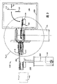
Fig. 1 is the top view of ion implantor terminal identity, and terminal identity is used to load workpiece to ion implantor, takes out the workpiece of processing from ion implantor;
Fig. 2 is the enlarged drawing of a part of the terminal identity of Fig. 1;
Fig. 3 is the schematic diagram that shows the vacuum robot of upper and lower relatively top load lock, and robot is used to transmit workpiece to ion and injects terminal identity;
Fig. 4 is the enlarged drawing of a part of the vacuum robot of Fig. 3;
Fig. 4 A is the enlarged drawing that supports the robot housing of motor in housing, and the rotatable robot of motor arm transmits workpiece, is transferred to processing module from top load lock;
Fig. 4 B is the enlarged drawing of gate valve, and gate valve is used for making the vacuum robot near load lock interior;
Fig. 5 is the adjacent upper and lower top load lock and the end view of vacuum separation valve, and vacuum separation valve can allow workpiece to move into and shift out top load lock;
Fig. 6 and Fig. 7 show that the workpiece before and after the ion beam processing workpiece moves order; With
Fig. 8 shows the advance figure of step or position of representativeness that workpiece advances at the terminal identity of Fig. 1.
Embodiment
Get back to accompanying drawing now, Fig. 1 and 3 has shown terminal identity 110, its be used for the ion beam processing device under low pressure or vacuum to workpiece, as semiconductor wafer 112, process.Terminal identity comprises two work-piece isolation load locks 116,117 (see figure 3)s, is used for from higher-pressure region 118 (generally under atmospheric pressure) transmission workpiece (generally being semiconductor wafer) to low-pressure area 120, and can returns higher-pressure region 118.In illustrated exemplary embodiment, two top load lock 116,117 are stacked mutually.
A purposes of terminal identity shown in Figure 1 is to inject ion to a semiconductor wafer of ion beam B continuously at every turn, and ion beam enters into ion and injects chamber 130, and its inside is in the low pressure condition.Robot 132 is arranged to and can workpiece be set injects chamber 130 to ion from two top load lock, 116,117 one of them taking-up workpiece.Robot 132 can be from two top load lock 116,117 any transferring wafer, transfer wafers is to the anchor clamps that are positioned at band to band transfer module 134.At band to band transfer module 134, robot 132 is set to wafer chuck 135 with wafer, and it can attract workpiece and workpiece is fixed to appropriate location on the anchor clamps.These wafer chucks are known in the prior art.Anchor clamps and workpiece turn to the appropriate location then, and workpiece is injected into the ion among the ion beam B in this position.Anchor clamps 135 rotate about an angle of 90 degrees (wafer or workpiece 112 are in vertical position, as shown in Figure 3) after, the ion beam B that injects chamber 130 is to scanning before and after the wafer, shown in arrow 137.
According to exemplary embodiment of the present invention, ion beam B utilizes the electrode (not shown) to scan opposite side from a side, and electrode is positioned at the upstream of the ion beam path before the arrival ion injection chamber 130.It is known in prior art to the injection wafer mechanism of opposite side scanning that other need not carry out a side.One side is to the fan-shaped ion beam of opposite side scanning formation.This shape is in conjunction with the scanning up and down of workpiece, and shown in arrow 137, but machined surface is to the whole work-piece surface of ion beam.
After the ion beam processing (only need several seconds), wafer chuck rotates back into band to band transfer module, and robot 132 takes out workpiece, and the workpiece that processes is moved back in the top load lock 116,117 one, transmits go back to higher-pressure region 118.In the embodiment that is introduced, robot 132 comprises two active margin clamping end effector, have two arms separately, when top load lock 116, during 117 travelling workpiece transmission back platforms, any end effector can be controlled the workpiece in the top load lock, and top load lock 116,117 moves along curved path P (see figure 1) relatively.
Exemplary embodiment of the present invention can be carried out ion beam processing to semiconductor wafer in conjunction with the ion implantor in the IC processing equipment.Fig. 1 has schematically shown the unified cabin 140-143 of 4 open fronts, is used for the integrated circuit manufacturing equipment and installs to another from a mobile silicon wafer of device.Overhead transport sector (not shown) can be provided with the position of these 4 cabins to relative terminal identity 110 respectively, is arranged in two scopes that robot 146,148 can both reach of atmosphere, makes the robot arm to take out one or more silicon wafers from the processing cabin.Wafer can be controlled by robot in the atmosphere, and wafer is set to aligner 150, but the aligner positions wafer is inserted one of wafer to two top load lock 116,117 then in the appropriate location.
Fig. 3,4, the end view of 4A has shown the details of robot 132 in the vacuum, this robot can move wafer to low-pressure area 120 from top load lock 116,117.Robot 132 comprises two concentric normally vertically disposed driving shafts 210,211, and driving shaft is connected to motor 214,215 (seeing Fig. 4 A), and motor support is in robot housing 216.Driving shaft be subjected to being positioned at housing 216 tops flowing molten iron body seal 217 support and therefrom pass through.Interior driving shaft 210 can rotate under motor 215 drives, selectivity location first end controls, and it has robot arm 220,221, and arm radially extends to controlled location around center line 224 from upper supporting piece 222.Second lower support element 223 is connected to driving shaft 211, and supports the second end controls, and it has arm 220a, and 221a can carry out controlled rotation around center line 224.At the partial cross section figure of Fig. 2, axle 211 has turned to arm 220a, and 221a controls the position of wafer in the end or the following top load lock 117.In the end view of Fig. 3 and Fig. 4, upper end controls arm 220,221 turns to the position that wafer anchor clamps 135 on band to band transfer module are set by controlled actuation motor 215.
Pneumatic actuator (not shown) in the robot can make a pivoted arm 220 relative fixed arms 221 be pivoted, but controlled actuation is (by controller 200, its scalable wafer moves through terminal identity 10 as shown in Figure 1), to control pivoted arm 220 and the fixing wafer between the arm 221.When pivoted arm 220 moved contact wafer, as wafer 112, the contact mat 226 that is connected two arms was at three some joint wafers along Waffer edge.In case wafer is controlled by arm, be connected to the reposition of the revolution wafer of end effector arm to the rotation centerline 224 of relative robot 132.
Shown in Fig. 4 A, motor 214,215 and relevant driving shaft 210,211 are connected to carriage 228, allow two end effector to move up and down along the z shown in Fig. 4 simultaneously.The realization of moving is that it has the output shaft that is connected to ball screw by motor 225 (seeing Fig. 4 A), and ball screw is connected to supporting plate 228.Motor 225 by controller 200 controlled energization moves up and down supporting plate 228 along line slideway 229.Supporting plate 228 stop or holding position 290 (see figure 1)s along z to two end effector of controlled up and down mobile permission robot in any enters any top load lock.Another kind of mode, the arm 220,221 of first end controls can insert any top load lock 116,117, and to control wafer, the arm 220a of the second end controls, 221a also can insert any top load lock 116 or 117.For mobile wafer then to the processing module that is positioned at the band to band transfer module that injects the chamber, wafer can re-position at z to, if it will take out from last top load lock 116.
With reference to figure 4, flowing molten iron body seal 217 is subjected to being connected to the restriction of the expandable extensible member 227 of supporting plate 228 around its periphery, and when motor when moveable support 222,223 is to the position of arm up and down along z, extensible member shrinks.These extensible members 227 permission extensible members radially exterior domain remain under the atmospheric pressure effect, and the wafer zone that the front and back rotation is passed through between band to band transfer module and top load lock remains in low pressure or vacuum.
Top load lock 116,117 has two openings respectively, facing to the higher-pressure region, is used to the wafer that inserts raw wafer and process from the top load lock taking-up.Last top load lock 116 comprises two openings 230,231, can open and close by hermatic door, and hermatic door seals the outward surface of top load lock by controller 200 at the appropriate time of injection technology.Similar fashion, following top load lock 117 comprises two openings 232,233, can open and close by hermatic door, seals the outward surface of top load lock at the appropriate time hermatic door of injection technology.
For wafer being set to top load lock, suitable gate valve or gate must be removed from corresponding opening, by one in the robot in the atmosphere 146,148 wafer are inserted into top load lock.In the end view of Fig. 4, demonstrate top load lock opening 230,232, the end effector 280 of robot 148 demonstrates the opening 230 of going up top load lock relatively and is provided with.End effector 280 is inserted wafer top load lock and wafer is placed into starlike strutting piece 240, it has arm 241,242,243 (see figure 2)s of radially extending, the arm supporting wafers is in certain position, and this position allows wafer to be controlled by the end effector of robot in the vacuum 132.For controlling wafer and mobile wafer to band to band transfer module, the robot arm rotates one that is fit to by in two openings 260,262, as shown in Figure 4.
Shown in the end view of Fig. 4, top load lock comprises two transparent windows 244,245, is provided with two optical pickocffs 246,247 near window, is used for monitoring wafer and is transferred to top load lock.The existence and the aligning of the wafer on the starlike strutting piece 240 of sensor transfer back to controller 200 with signal.
Fig. 5 has shown upper and lower top load lock 116,117 and has opened and closed the structure of top load lock, so that insert and take out wafer by robot in the air.Last top load lock has two gate valves 266,267, and valve comprises two plates, is inclined to about 90 degree relative to each other, and is connected to pneumatic actuator 268,269.Plate has such angle and means that any robot 146,148 can obtain wafer or transfer wafers to top load lock from top load lock.Similarly, following top load lock has two gate valves 270,271, and is connected to pneumatic actuator 272,273.Each valve is arranged in an opening of top load lock separately.Valve comprises perimeter seal, and the aeroseal that extends to guarantee plate and corresponding opening around plate engages.For wafer can be inserted in the opening, plate is at first removed along the direction that is orthogonal to the top load lock outer surface usually from its opening.Outwards the realization of moving is the piston 274 (for example) by being connected to plate.In case plate and opening are fully spaced apart by piston, coupled actuator moves the enough distances of relevant plate from top load lock along the path lateral of leaving top load lock, make the end effector 280 of airborne robot can insert the opening of wafer, wafer is set to starlike strutting piece 240 to top load lock.The cover plate of valve 271 moves down, as up and down shown in the arrow of Fig. 5.Plate hydrodynamic reciprocating sealing opening is to realize by the actuating of piston of controller 200 control specific actuator with opening sealing.
At the inlet side of top load lock, system comprises the upper and lower actuator 275,276 that is connected to gate valve 277,278.Valve and actuator are subjected to the support of valve housing 281.With reference to figure 4 and 4B, valve housing 281 is arranged between top load lock 116,117 and the robot housing 216.Gate valve 277,278 moves up and down along the z direction, opens and closes the opening 269,262 that leads to load lock interior, and the arm rotation of robot is moved wafer turnover region of no pressure by opening.Shown in Fig. 4 B, gate valve 277 is provided with piston and plate, plate supporting sealing member 283, the surface of the formation opening 260 of the salable joint gate valve of seal housing 281.Extensible member 279 allow the actuator 275 of top load lock to be arranged in atmosphere, and gate is arranged in low pressure or vacuum around the piston of gate valve.
In the centre position of two top load lock 116,117 and band to band transfer module, terminal identity 110 comprises parking platform 290, and the wafer that robot can control it temporarily is parked in parking platform.Under situation about being fit to, two end effectors move to this parking platform 290, and arm can have wafer or not have.As shown in Figure 6, the arm 220a of robot, the bottom controls of 221a rests in this position, and arm is keeping wafer.The mobile of docking station is important initial step, then the controlled actuation of motor 225 reacted, and two end effector of robot arm go up simultaneously or move down.
Fig. 6 demonstrates, and at the terminal identity 110 of implanter, processes the order or the wafer path (seeing arrow shown in Figure 6) of the working motion of a plurality of workpiece continuously under low pressure or vacuum.This order of steps also is presented in the chart of Fig. 8.The first step among the figure, from being arranged in the FOUP142 of elevated pressures district 118 (atmosphere), wafer (step 300 of Fig. 8) is collected or picked up in robot 148.Robot 148 shifts out wafer and places wafer in aligner 150 (step 301) from FOUP 142.Aligner is alignment wafer (step 302) then.Second airborne robot 146 in Fig. 6 takes out or picks up wafer and it is moved to first time top load lock 117 (step 303) from aligner 150, and raw wafer is put into top load lock 117 (step 304).Top load lock 117 is connected to valve V2, and valve is communicated with load lock interior to pump 204 (step 305), and after lid 270 had been placed on opening 232, pump can reduce the pressure in the top load lock.Can see that with reference to figure 5 top load lock 117 is downward by pump, this does not mean that top load lock 116 is under the specified pressure, is connected to independent actuated valve V1 because go up top load lock 116, and two top load lock are isolated mutually.
After wafer was injected (step 308) by ion beam B ion, robot 132 took out wafer and returns (step 309) by curved path P, and the workpiece that processes is put into down top load lock 117 (step 310).Controller 200 is communicated with top load lock 117 (step 311) down by valve V2 then, and airborne robot 148 takes off the workpiece (step 312) that processes from following top load lock 117, and it is sent back to FOUP142 (step 313).
Each follow-up undressed wafer for picking up from FOUP 142 repeats this a series of transmission path.When top load lock 117 is communicated with, when the wafer that allows to process moves back to FOUP142, take out the wafer that processes after robot 146 raw wafer is set to bottom controls 117.Similarly, after wafer to be processed took out from top load lock, the second end controls of the arm of robot can insert the top load lock of finding time with the wafer that has processed in the vacuum.
As shown in Figure 8, a plurality of wafers can transmit along the path of Fig. 6 simultaneously.The wafer that processes send back to other before three the wafer injecting programs of FOUP142 (step 313) start (be in step 300a, 300b, 300c).Wafer joins between two top load lock, make that next program begins to take out wafers (step 300a) from FOUP 142 during, wafer transport is to upper end controls 116.In illustrated embodiment, wafer enters vacuum and leaves vacuum and use same top load lock after ion beam processing, though this is not that enforcement is of the presently claimed invention.Exemplary embodiment demonstrates, and is T second if get back to the complete mobile of FOUP142 from FOUP142, and moves 4 wafers simultaneously, reduces to T/4 second the average time of each wafer.
Fig. 8 has shown the order of wafer by step.The time that the x axle representative of this figure increases.Have identical length though different step demonstrates, be to be understood that to have the different time as the different step 1, in the process of exemplifying embodiment embodiment, these different times of steps cost.
Fig. 7 has shown that another kind of processing is moved or the order of wafer path (seeing the arrow among Fig. 7), is used under low pressure or the vacuum and processes a plurality of workpiece continuously at implanter terminal identity 110.Robot 146 takes out wafer from the FOUP141 that is positioned at higher-pressure region 118 (under the atmosphere).Robot 146 moves wafer to aligner 150 from FOUP142.Second airborne robot 148 takes off wafer from aligner 150, moves to top load lock 116 on first, and raw wafer is placed into top load lock 116.
First top load lock 116 is found time to reduce pressure by pump 204, in case vacuumize, valve plate 277 is actuated device 275 and opens.Robot 132 in the vacuum moves end effector and enters top load lock 116, takes out raw wafer from the inside of first top load lock.
After ion beam processing, robot 132 takes out wafer, and P sends back to by curved path, and the workpiece that processes is placed into top load lock 116 second time.Controller 200 is communicated with second top load lock by valve V1 then, and airborne robot 146 takes out the workpiece that processes from following top load lock 116, sends back FOUP 141.The common trait of Fig. 6 and each transmission path shown in Figure 7 is that aligner 150 will be passed through in the path that moves to top load lock.
The present invention introduces with certain particularity.The time that table one shows can not be used to limit the scope of the invention, and the order of procedure of processing can not be used for limiting the present invention.Will be appreciated that the present invention includes all improvement and variation to disclosed exemplary embodiment, these changes and improvements do not break away from the spirit and scope of claims.
Claims (23)
1. work-piece transmission system that together uses with the equipment of processing work under low pressure, described system comprises:
A) be contained in first isolation load locks in the top load lock housing, it is used for workpiece is transferred to low-pressure area and makes it to return described higher-pressure region from the higher-pressure region, and comprise with first and second openings of different angle faces, to allow to come near described first top load lock from two different directions to described higher-pressure region;
B) be contained in second isolation load locks in the top load lock housing, it is positioned near first work-piece isolation load locks, be used for workpiece is transferred to low-pressure area and makes it to return described higher-pressure region from the higher-pressure region, and comprise with first and second openings of different angle faces, to allow to come near described second top load lock from two different directions to described higher-pressure region;
C) workpiece machine table is used for processing work under low pressure; With
D) first robot, it is used for workpiece is transferred to the workpiece machine table from one of them of described first and second work-piece isolation load locks; With
E) be positioned in the described higher-pressure region and be arranged in a plurality of air robot outside the described low-pressure area, be used for before workpiece being processed and made described workpiece arrival destination locations after the described processing, described workpiece is sent to adjacent work-piece isolation load locks to and fro from the source of described workpiece, wherein, in described a plurality of air in the robot each all is aligned to the opening towards appointment, an opening of the appointment of described first and second openings that are used for making workpiece move through given top load lock.
2. transmission system according to claim 1 is characterized in that described system also comprises the workpiece alignment device, is used to control the aligning of the workpiece mobile by first and second work-piece isolation load locks.
3. transmission system according to claim 1 is characterized in that, each described top load lock comprises supporting member, is used to support the workpiece on the supporting member that is positioned at described top load lock; With
By-pass valve control, it selectively is communicated to top load lock atmosphere and is communicated to vacuum source, to reduce the pressure in the described top load lock.
4. transmission system according to claim 1, it is characterized in that, described first and second isolation load locks are vertically spaced apart, and described first robot comprises two isolated end effector, are movable to first and second isolation load locks to obtain workpiece.
5. transmission system according to claim 4 is characterized in that, isolated end effector top load lock relatively rises and descends, and allows arbitrary end effector to move to described first or second top load lock.
6. transmitting device that together uses with the equipment of processing work under low pressure, described transmitting device comprises:
A) obturator, it has formed low-pressure area, and the workpiece machine table that is used in described low-pressure area is processed workpiece;
B) two adjacent work-piece isolation load locks, wherein each top load lock comprises:
I) first and second openings, it selectively is communicated to load lock interior with atmospheric pressure, is used for to and fro conveying work pieces to atmospheric pressure region, and wherein, described first and second openings come in the face of described atmospheric pressure region with different angles; With
Ii) the 3rd opening, it is used for that the workpiece in the described top load lock is delivered to low-pressure area processes, and turns back to the atmospheric pressure region of described more high pressure after described processing;
C) first robot is used for the machine table from adjacent work-piece isolation load locks transmission workpiece to low-pressure area; With
D) be positioned in the described atmospheric pressure region and be arranged in a plurality of air robot outside the described low-pressure area, be used for before workpiece being processed and made described workpiece arrival destination locations after the described processing, described workpiece is sent to adjacent work-piece isolation load locks to and fro from the source of described workpiece, wherein, in described a plurality of air in the robot each all is aligned to the opening towards appointment, an opening of the appointment of described first and second openings that are used for making workpiece move through given top load lock.
7. transmitting device according to claim 6 is characterized in that, described adjacent work-piece isolation load locks is stacked mutually.
8. transmitting device according to claim 7 is characterized in that, described first and second openings of top load lock can be opened, and inserts and places on the supporting member of top load lock along different mobile routes to allow workpiece.
9. transmitting device according to claim 6 is characterized in that, the workpiece in the described first robot moving electric arc is to band to band transfer module.
10. transmitting device according to claim 9 is characterized in that, described first robot has two end effector, and wherein each end effector can initiatively be controlled the workpiece in each top load lock.
11. transmitting device according to claim 10 is characterized in that, described top load lock is stacked mutually, and described workpiece generally is a plane wafer, and two end effector move up and down along the direction transverse to the plane of the wafer that is generally the plane in addition.
12. transmitting device according to claim 11 is characterized in that, described two end effector are connected to movably carrier, and carrier can move two end effector simultaneously.
13. one kind is used under low pressure the method for a plurality of workpiece of processing continuously, it comprises:
Two top load lock are positioned to adjacent one another are, wherein, each top load lock all has the first and second atmospheric pressure openings, they with different angle faces to atmospheric pressure region;
The low pressure robot is provided, and it has two end effector, is used for workpiece is moved to machine table from described these two top load lock;
With robot in a plurality of air be positioned to described these two top load lock in the atmospheric pressure opening of appointment form the relation face, to be used to making workpiece move described these two top load lock of coming in and going out;
Utilize that robot catches unprocessed workpiece in the air, and described unprocessed workpiece is moved in first top load lock of described these two top load lock by first air pressure-loading locking piece opening, robot forms the relation of facing in wherein said first air pressure-loading locking piece opening and described this air, and, described unprocessed workpiece is placed described first top load lock;
Reduce the pressure in first top load lock;
Utilize an end effector of described low pressure robot to take out unprocessed workpiece, unprocessed workpiece is moved to machine table from first top load lock;
Utilize the second end controls of described low pressure robot to be placed into from the workpiece of having processed that machine table obtains one of them top load lock of described two top load lock;
Improve described this load lock interior pressure; With
By the atmospheric pressure top load lock opening of appointment, and take out the workpiece of having processed from top load lock.
14. method according to claim 13 is characterized in that, the workpiece setting that processes is in a top load lock, and unprocessed workpiece is processed in machine table.
15. method according to claim 14 is characterized in that, workpiece is a semiconductor wafer, and its mesolow robotic delivery wafer also places the wafer chuck that can attract wafer with wafer, also is included in to reorientate wafer and anchor clamps before processing.
16. method according to claim 13 is characterized in that, also comprises, described two top load lock is positioned at mode on another with one and self location, ground.
17. method according to claim 16 is characterized in that, moves up and down two end effector of low pressure robot, makes any end effector near the workpiece in any top load lock of described these two top load lock.
18. method according to claim 17 is characterized in that, described two mutual conllinear of end effector are installed on carrier, and carrier supporting CD-ROM drive motor can be actuated each end effector separately; Also comprise, move up and down described carrier, suitably locate end effector with respect to top load lock with respect to described these two top load lock.
19. method according to claim 13 is characterized in that, described workpiece generally is a plane wafer, also is included in raw wafer is inserted into to align wafer position before first top load lock.
20. method according to claim 19, it is characterized in that, also comprise, utilize that robot picks up raw wafer from wafer source in first air, described raw wafer is placed into aligner to be positioned, wherein, robot takes out the wafer of aiming at from aligner in second air, is transferred to machine table by top load lock.
21. method according to claim 13, it is characterized in that, one or more other unprocessed workpiece move to described first top load lock continuously by robot in the air from the workpiece source, then, take out the workpiece of having processed from described this top load lock.
22. method according to claim 21, it is characterized in that, some other unprocessed workpiece setting another top load lock in described these two top load lock, the workpiece of front is taken off in permission from the top load lock under the pump, another top load lock is opened the connection atmosphere simultaneously, to accept unprocessed workpiece.
23. method according to claim 13 is characterized in that, given workpiece takes off from top load lock after processing, and this top load lock is described given workpiece residing same top load lock before processing.
Applications Claiming Priority (2)
| Application Number | Priority Date | Filing Date | Title |
|---|---|---|---|
| US10/826,419 | 2004-04-16 | ||
| US10/826,419 US7246985B2 (en) | 2004-04-16 | 2004-04-16 | Work-piece processing system |
Publications (2)
| Publication Number | Publication Date |
|---|---|
| CN1943009A CN1943009A (en) | 2007-04-04 |
| CN100437898C true CN100437898C (en) | 2008-11-26 |
Family
ID=35096438
Family Applications (1)
| Application Number | Title | Priority Date | Filing Date |
|---|---|---|---|
| CNB2005800115339A Expired - Fee Related CN100437898C (en) | 2004-04-16 | 2005-04-18 | Work-piece processing system |
Country Status (7)
| Country | Link |
|---|---|
| US (2) | US7246985B2 (en) |
| EP (1) | EP1735822A2 (en) |
| JP (1) | JP2007533167A (en) |
| KR (1) | KR101276014B1 (en) |
| CN (1) | CN100437898C (en) |
| TW (1) | TWI347295B (en) |
| WO (1) | WO2006041530A2 (en) |
Cited By (1)
| Publication number | Priority date | Publication date | Assignee | Title |
|---|---|---|---|---|
| CN102484090A (en) * | 2009-07-14 | 2012-05-30 | 佳能安内华股份有限公司 | Substrate processing device |
Families Citing this family (45)
| Publication number | Priority date | Publication date | Assignee | Title |
|---|---|---|---|---|
| US20040221811A1 (en) * | 2001-11-30 | 2004-11-11 | Robert Mitchell | Method and apparatus for processing wafers |
| US20060045668A1 (en) * | 2004-07-19 | 2006-03-02 | Grabowski Al W | System for handling of wafers within a process tool |
| US7720558B2 (en) * | 2004-09-04 | 2010-05-18 | Applied Materials, Inc. | Methods and apparatus for mapping carrier contents |
| US9110456B2 (en) * | 2004-09-08 | 2015-08-18 | Abb Research Ltd. | Robotic machining with a flexible manipulator |
| JP4907077B2 (en) * | 2004-11-30 | 2012-03-28 | 株式会社Sen | Wafer processing apparatus, wafer processing method, and ion implantation apparatus |
| JP2008525125A (en) * | 2004-12-22 | 2008-07-17 | インテリジェント ホスピタル システムズ リミテッド | Automatic dispensing system (APAS) |
| US7604449B1 (en) * | 2005-06-27 | 2009-10-20 | Kla-Tencor Technologies Corporation | Equipment front end module |
| US7534080B2 (en) * | 2005-08-26 | 2009-05-19 | Ascentool, Inc. | Vacuum processing and transfer system |
| US7381969B2 (en) * | 2006-04-24 | 2008-06-03 | Axcelis Technologies, Inc. | Load lock control |
| US8153513B2 (en) * | 2006-07-25 | 2012-04-10 | Silicon Genesis Corporation | Method and system for continuous large-area scanning implantation process |
| US7740437B2 (en) | 2006-09-22 | 2010-06-22 | Asm International N.V. | Processing system with increased cassette storage capacity |
| JP4664264B2 (en) * | 2006-10-26 | 2011-04-06 | 東京エレクトロン株式会社 | Detection apparatus and detection method |
| US20080138178A1 (en) * | 2006-12-06 | 2008-06-12 | Axcelis Technologies,Inc. | High throughput serial wafer handling end station |
| US7585142B2 (en) * | 2007-03-16 | 2009-09-08 | Asm America, Inc. | Substrate handling chamber with movable substrate carrier loading platform |
| US8267636B2 (en) | 2007-05-08 | 2012-09-18 | Brooks Automation, Inc. | Substrate transport apparatus |
| US8823294B2 (en) | 2007-06-27 | 2014-09-02 | Brooks Automation, Inc. | Commutation of an electromagnetic propulsion and guidance system |
| US9752615B2 (en) | 2007-06-27 | 2017-09-05 | Brooks Automation, Inc. | Reduced-complexity self-bearing brushless DC motor |
| US8659205B2 (en) | 2007-06-27 | 2014-02-25 | Brooks Automation, Inc. | Motor stator with lift capability and reduced cogging characteristics |
| KR101660894B1 (en) | 2007-06-27 | 2016-10-10 | 브룩스 오토메이션 인코퍼레이티드 | Multiple dimension position sensor |
| CN101790673B (en) | 2007-06-27 | 2013-08-28 | 布鲁克斯自动化公司 | Position feedback for self bearing motor |
| US8283813B2 (en) * | 2007-06-27 | 2012-10-09 | Brooks Automation, Inc. | Robot drive with magnetic spindle bearings |
| CN101801817B (en) | 2007-07-17 | 2015-07-22 | 布鲁克斯自动化公司 | Substrate processing apparatus with motors integral to chamber walls |
| JP5465979B2 (en) * | 2009-10-26 | 2014-04-09 | 東京エレクトロン株式会社 | Semiconductor manufacturing equipment |
| JP5476171B2 (en) * | 2010-03-16 | 2014-04-23 | 株式会社日立ハイテクノロジーズ | Vacuum processing equipment |
| JP5755842B2 (en) * | 2010-04-22 | 2015-07-29 | 株式会社ダイヘン | Work transfer system |
| CN102310999B (en) * | 2010-07-09 | 2013-07-17 | 上海凯世通半导体有限公司 | Vacuum transmission process equipment and method |
| JP5503006B2 (en) * | 2010-08-06 | 2014-05-28 | 東京エレクトロン株式会社 | Substrate processing system, transfer module, substrate processing method, and semiconductor device manufacturing method |
| WO2012098871A1 (en) * | 2011-01-20 | 2012-07-26 | 東京エレクトロン株式会社 | Vacuum processing apparatus |
| JP5494617B2 (en) * | 2011-10-26 | 2014-05-21 | 株式会社安川電機 | Robot system and method of manufacturing processed product |
| CN102539263A (en) * | 2011-11-29 | 2012-07-04 | 南通大学 | Slight abrasion measurement method based on shelter processing technology |
| US9139402B2 (en) * | 2012-02-21 | 2015-09-22 | Altec Industries, Inc. | Retractable load guide |
| JP6002532B2 (en) * | 2012-10-10 | 2016-10-05 | 株式会社日立ハイテクノロジーズ | Vacuum processing apparatus and vacuum processing method |
| US10328580B2 (en) * | 2013-08-09 | 2019-06-25 | Persimmon Technologies Corporation | Reduced footprint substrate transport vacuum platform |
| CN104016175A (en) * | 2014-05-26 | 2014-09-03 | 王义峰 | Automatic outputting mechanism of screen printer |
| JP6257455B2 (en) * | 2014-06-17 | 2018-01-10 | 住友重機械イオンテクノロジー株式会社 | Ion implantation apparatus and control method of ion implantation apparatus |
| US9378992B2 (en) | 2014-06-27 | 2016-06-28 | Axcelis Technologies, Inc. | High throughput heated ion implantation system and method |
| US9776807B2 (en) * | 2014-10-29 | 2017-10-03 | Alain Cerf | Changing orientation of an article on a moving conveyor |
| JP2017513036A (en) * | 2014-11-14 | 2017-05-25 | マッパー・リソグラフィー・アイピー・ビー.ブイ. | Cargo fixing system and method for transferring a substrate in a lithography system |
| US9607803B2 (en) | 2015-08-04 | 2017-03-28 | Axcelis Technologies, Inc. | High throughput cooled ion implantation system and method |
| US10559483B2 (en) * | 2016-08-10 | 2020-02-11 | Lam Research Corporation | Platform architecture to improve system productivity |
| JP6493339B2 (en) * | 2016-08-26 | 2019-04-03 | 村田機械株式会社 | Transport container and method for transferring contents |
| JP7275039B2 (en) * | 2017-03-15 | 2023-05-17 | ラム リサーチ コーポレーション | Space-saving platform architecture with linear vacuum transfer module |
| CN108695217B (en) * | 2017-04-07 | 2021-06-29 | 台湾积体电路制造股份有限公司 | Substrate transport apparatus and edge effector therefor |
| JP7210960B2 (en) * | 2018-09-21 | 2023-01-24 | 東京エレクトロン株式会社 | Vacuum processing apparatus and substrate transfer method |
| US11581203B2 (en) * | 2020-09-02 | 2023-02-14 | Applied Materials, Inc. | Systems for integrating load locks into a factory interface footprint space |
Citations (5)
| Publication number | Priority date | Publication date | Assignee | Title |
|---|---|---|---|---|
| US4498832A (en) * | 1982-05-21 | 1985-02-12 | The Boc Group, Inc. | Workpiece accumulating and transporting apparatus |
| CN1320954A (en) * | 1994-07-28 | 2001-11-07 | 株式会社半导体能源研究所 | Laser treating method |
| US6350097B1 (en) * | 1999-04-19 | 2002-02-26 | Applied Materials, Inc. | Method and apparatus for processing wafers |
| CN1348552A (en) * | 1999-04-02 | 2002-05-08 | 硅谷集团热系统责任有限公司 | Semiconductor wafer processing system with vertically-stacked process chambers and single-axis dual-wafer transfer system |
| US6647665B1 (en) * | 1997-11-28 | 2003-11-18 | Mattson Technology, Inc. | Door systems for low contamination, high throughput handling of workpieces for vacuum processing |
Family Cites Families (24)
| Publication number | Priority date | Publication date | Assignee | Title |
|---|---|---|---|---|
| US5003183A (en) * | 1989-05-15 | 1991-03-26 | Nissin Electric Company, Limited | Ion implantation apparatus and method of controlling the same |
| US5186718A (en) * | 1989-05-19 | 1993-02-16 | Applied Materials, Inc. | Staged-vacuum wafer processing system and method |
| KR0155158B1 (en) * | 1989-07-25 | 1998-12-01 | 카자마 젠쥬 | Vertical wafer treatment apparatus and the method |
| JPH04298060A (en) * | 1991-03-26 | 1992-10-21 | Tokyo Electron Ltd | Load lock apparatus and wafer transfer system and detection of wafer position |
| US5376212A (en) * | 1992-02-18 | 1994-12-27 | Tokyo Electron Yamanashi Limited | Reduced-pressure processing apparatus |
| JP2531910Y2 (en) * | 1992-03-31 | 1997-04-09 | 株式会社スガイ | Article gripping device |
| US5482607A (en) * | 1992-09-21 | 1996-01-09 | Nissin Electric Co., Ltd. | Film forming apparatus |
| US5486080A (en) * | 1994-06-30 | 1996-01-23 | Diamond Semiconductor Group, Inc. | High speed movement of workpieces in vacuum processing |
| TW295677B (en) * | 1994-08-19 | 1997-01-11 | Tokyo Electron Co Ltd | |
| JP3215643B2 (en) * | 1997-01-31 | 2001-10-09 | ワイエイシイ株式会社 | Plasma processing equipment |
| JPH11307608A (en) * | 1998-04-16 | 1999-11-05 | Nissin Electric Co Ltd | Processed piece carrier system |
| JP2000012647A (en) * | 1998-06-19 | 2000-01-14 | Sumitomo Eaton Noba Kk | Device and method for carrying wafer |
| JP2000208589A (en) * | 1998-11-09 | 2000-07-28 | Tokyo Electron Ltd | Apparatus for processing |
| JP2000174091A (en) * | 1998-12-01 | 2000-06-23 | Fujitsu Ltd | Carrying device and manufacturing device |
| GB2349269A (en) * | 1999-04-19 | 2000-10-25 | Applied Materials Inc | Ion implanter |
| JP2000323551A (en) * | 1999-05-11 | 2000-11-24 | Anelva Corp | Substrate processing apparatus |
| JP4316752B2 (en) * | 1999-11-30 | 2009-08-19 | キヤノンアネルバ株式会社 | Vacuum transfer processing equipment |
| JP3973006B2 (en) | 2000-03-23 | 2007-09-05 | 日本電産サンキョー株式会社 | Double arm robot |
| US6977014B1 (en) * | 2000-06-02 | 2005-12-20 | Novellus Systems, Inc. | Architecture for high throughput semiconductor processing applications |
| US6860965B1 (en) * | 2000-06-23 | 2005-03-01 | Novellus Systems, Inc. | High throughput architecture for semiconductor processing |
| US6918731B2 (en) * | 2001-07-02 | 2005-07-19 | Brooks Automation, Incorporated | Fast swap dual substrate transport for load lock |
| US6663333B2 (en) * | 2001-07-13 | 2003-12-16 | Axcelis Technologies, Inc. | Wafer transport apparatus |
| SG115630A1 (en) * | 2003-03-11 | 2005-10-28 | Asml Netherlands Bv | Temperature conditioned load lock, lithographic apparatus comprising such a load lock and method of manufacturing a substrate with such a load lock |
| US7010388B2 (en) * | 2003-05-22 | 2006-03-07 | Axcelis Technologies, Inc. | Work-piece treatment system having load lock and buffer |
-
2004
- 2004-04-16 US US10/826,419 patent/US7246985B2/en active Active
-
2005
- 2005-04-15 TW TW094111981A patent/TWI347295B/en active
- 2005-04-18 EP EP05823455A patent/EP1735822A2/en not_active Withdrawn
- 2005-04-18 JP JP2007508638A patent/JP2007533167A/en active Pending
- 2005-04-18 CN CNB2005800115339A patent/CN100437898C/en not_active Expired - Fee Related
- 2005-04-18 WO PCT/US2005/013273 patent/WO2006041530A2/en active Application Filing
- 2005-04-18 KR KR1020067024015A patent/KR101276014B1/en active IP Right Grant
-
2007
- 2007-06-20 US US11/765,499 patent/US7699574B2/en active Active
Patent Citations (5)
| Publication number | Priority date | Publication date | Assignee | Title |
|---|---|---|---|---|
| US4498832A (en) * | 1982-05-21 | 1985-02-12 | The Boc Group, Inc. | Workpiece accumulating and transporting apparatus |
| CN1320954A (en) * | 1994-07-28 | 2001-11-07 | 株式会社半导体能源研究所 | Laser treating method |
| US6647665B1 (en) * | 1997-11-28 | 2003-11-18 | Mattson Technology, Inc. | Door systems for low contamination, high throughput handling of workpieces for vacuum processing |
| CN1348552A (en) * | 1999-04-02 | 2002-05-08 | 硅谷集团热系统责任有限公司 | Semiconductor wafer processing system with vertically-stacked process chambers and single-axis dual-wafer transfer system |
| US6350097B1 (en) * | 1999-04-19 | 2002-02-26 | Applied Materials, Inc. | Method and apparatus for processing wafers |
Cited By (3)
| Publication number | Priority date | Publication date | Assignee | Title |
|---|---|---|---|---|
| CN102484090A (en) * | 2009-07-14 | 2012-05-30 | 佳能安内华股份有限公司 | Substrate processing device |
| CN102484090B (en) * | 2009-07-14 | 2015-01-07 | 佳能安内华股份有限公司 | Substrate processing device |
| US9245785B2 (en) | 2009-07-14 | 2016-01-26 | Canon Anelva Corporation | Substrate processing apparatus |
Also Published As
| Publication number | Publication date |
|---|---|
| EP1735822A2 (en) | 2006-12-27 |
| TW200540087A (en) | 2005-12-16 |
| CN1943009A (en) | 2007-04-04 |
| US7699574B2 (en) | 2010-04-20 |
| US7246985B2 (en) | 2007-07-24 |
| KR101276014B1 (en) | 2013-06-19 |
| KR20070012490A (en) | 2007-01-25 |
| US20050232727A1 (en) | 2005-10-20 |
| TWI347295B (en) | 2011-08-21 |
| JP2007533167A (en) | 2007-11-15 |
| WO2006041530A2 (en) | 2006-04-20 |
| US20070243049A1 (en) | 2007-10-18 |
| WO2006041530A3 (en) | 2006-06-08 |
Similar Documents
| Publication | Publication Date | Title |
|---|---|---|
| CN100437898C (en) | Work-piece processing system | |
| JP7263642B2 (en) | wafer aligner | |
| US11352220B2 (en) | Semiconductor wafer handling and transport | |
| JP6577944B2 (en) | Processing equipment including on-the-fly substrate centering | |
| CN100481314C (en) | Workpiece treatment system having load lock and buffer | |
| JP5323718B2 (en) | High-productivity continuous wafer processing equipment | |
| EP1684951B1 (en) | System for handling workpieces in a vacuum-based semiconductor handling system | |
| JP2007533167A5 (en) | ||
| JP2010512026A (en) | High productivity wafer notch alignment system | |
| US8083463B2 (en) | Mini clean room for preventing wafer pollution and using method thereof | |
| JPH07231028A (en) | Conveying apparatus and conveying method |
Legal Events
| Date | Code | Title | Description |
|---|---|---|---|
| C06 | Publication | ||
| PB01 | Publication | ||
| C10 | Entry into substantive examination | ||
| SE01 | Entry into force of request for substantive examination | ||
| C14 | Grant of patent or utility model | ||
| GR01 | Patent grant | ||
| CF01 | Termination of patent right due to non-payment of annual fee |
Granted publication date: 20081126 Termination date: 20200418 |
|
| CF01 | Termination of patent right due to non-payment of annual fee |