CN100423120C - Interference-free lms-based adaptive asynchronous receiver - Google Patents
Interference-free lms-based adaptive asynchronous receiver Download PDFInfo
- Publication number
- CN100423120C CN100423120C CNB038091305A CN03809130A CN100423120C CN 100423120 C CN100423120 C CN 100423120C CN B038091305 A CNB038091305 A CN B038091305A CN 03809130 A CN03809130 A CN 03809130A CN 100423120 C CN100423120 C CN 100423120C
- Authority
- CN
- China
- Prior art keywords
- sequence
- receiver
- centerdot
- adaptive
- loop
- Prior art date
- Legal status (The legal status is an assumption and is not a legal conclusion. Google has not performed a legal analysis and makes no representation as to the accuracy of the status listed.)
- Expired - Fee Related
Links
Images


Classifications
-
- G—PHYSICS
- G11—INFORMATION STORAGE
- G11B—INFORMATION STORAGE BASED ON RELATIVE MOVEMENT BETWEEN RECORD CARRIER AND TRANSDUCER
- G11B20/00—Signal processing not specific to the method of recording or reproducing; Circuits therefor
- G11B20/10—Digital recording or reproducing
-
- H—ELECTRICITY
- H04—ELECTRIC COMMUNICATION TECHNIQUE
- H04L—TRANSMISSION OF DIGITAL INFORMATION, e.g. TELEGRAPHIC COMMUNICATION
- H04L25/00—Baseband systems
- H04L25/02—Details ; arrangements for supplying electrical power along data transmission lines
- H04L25/03—Shaping networks in transmitter or receiver, e.g. adaptive shaping networks
- H04L25/03006—Arrangements for removing intersymbol interference
- H04L25/03012—Arrangements for removing intersymbol interference operating in the time domain
- H04L25/03019—Arrangements for removing intersymbol interference operating in the time domain adaptive, i.e. capable of adjustment during data reception
- H04L25/03038—Arrangements for removing intersymbol interference operating in the time domain adaptive, i.e. capable of adjustment during data reception with a non-recursive structure
-
- G—PHYSICS
- G11—INFORMATION STORAGE
- G11B—INFORMATION STORAGE BASED ON RELATIVE MOVEMENT BETWEEN RECORD CARRIER AND TRANSDUCER
- G11B20/00—Signal processing not specific to the method of recording or reproducing; Circuits therefor
- G11B20/10—Digital recording or reproducing
- G11B20/10009—Improvement or modification of read or write signals
-
- G—PHYSICS
- G11—INFORMATION STORAGE
- G11B—INFORMATION STORAGE BASED ON RELATIVE MOVEMENT BETWEEN RECORD CARRIER AND TRANSDUCER
- G11B20/00—Signal processing not specific to the method of recording or reproducing; Circuits therefor
- G11B20/10—Digital recording or reproducing
- G11B20/14—Digital recording or reproducing using self-clocking codes
- G11B20/1403—Digital recording or reproducing using self-clocking codes characterised by the use of two levels
-
- G—PHYSICS
- G11—INFORMATION STORAGE
- G11B—INFORMATION STORAGE BASED ON RELATIVE MOVEMENT BETWEEN RECORD CARRIER AND TRANSDUCER
- G11B20/00—Signal processing not specific to the method of recording or reproducing; Circuits therefor
- G11B20/10—Digital recording or reproducing
- G11B20/12—Formatting, e.g. arrangement of data block or words on the record carriers
- G11B2020/1264—Formatting, e.g. arrangement of data block or words on the record carriers wherein the formatting concerns a specific kind of data
- G11B2020/1288—Formatting by padding empty spaces with dummy data, e.g. writing zeroes or random data when de-icing optical discs
-
- G—PHYSICS
- G11—INFORMATION STORAGE
- G11B—INFORMATION STORAGE BASED ON RELATIVE MOVEMENT BETWEEN RECORD CARRIER AND TRANSDUCER
- G11B2220/00—Record carriers by type
- G11B2220/20—Disc-shaped record carriers
- G11B2220/25—Disc-shaped record carriers characterised in that the disc is based on a specific recording technology
- G11B2220/2537—Optical discs
- G11B2220/2541—Blu-ray discs; Blue laser DVR discs
-
- H—ELECTRICITY
- H04—ELECTRIC COMMUNICATION TECHNIQUE
- H04L—TRANSMISSION OF DIGITAL INFORMATION, e.g. TELEGRAPHIC COMMUNICATION
- H04L25/00—Baseband systems
- H04L25/02—Details ; arrangements for supplying electrical power along data transmission lines
- H04L25/03—Shaping networks in transmitter or receiver, e.g. adaptive shaping networks
- H04L25/03006—Arrangements for removing intersymbol interference
- H04L2025/03433—Arrangements for removing intersymbol interference characterised by equaliser structure
- H04L2025/03439—Fixed structures
- H04L2025/03445—Time domain
- H04L2025/03471—Tapped delay lines
- H04L2025/03477—Tapped delay lines not time-recursive
-
- H—ELECTRICITY
- H04—ELECTRIC COMMUNICATION TECHNIQUE
- H04L—TRANSMISSION OF DIGITAL INFORMATION, e.g. TELEGRAPHIC COMMUNICATION
- H04L25/00—Baseband systems
- H04L25/02—Details ; arrangements for supplying electrical power along data transmission lines
- H04L25/03—Shaping networks in transmitter or receiver, e.g. adaptive shaping networks
- H04L25/03006—Arrangements for removing intersymbol interference
- H04L2025/03592—Adaptation methods
- H04L2025/03598—Algorithms
- H04L2025/03611—Iterative algorithms
- H04L2025/03617—Time recursive algorithms
-
- H—ELECTRICITY
- H04—ELECTRIC COMMUNICATION TECHNIQUE
- H04L—TRANSMISSION OF DIGITAL INFORMATION, e.g. TELEGRAPHIC COMMUNICATION
- H04L7/00—Arrangements for synchronising receiver with transmitter
- H04L7/0054—Detection of the synchronisation error by features other than the received signal transition
- H04L7/0062—Detection of the synchronisation error by features other than the received signal transition detection of error based on data decision error, e.g. Mueller type detection
-
- H—ELECTRICITY
- H04—ELECTRIC COMMUNICATION TECHNIQUE
- H04L—TRANSMISSION OF DIGITAL INFORMATION, e.g. TELEGRAPHIC COMMUNICATION
- H04L7/00—Arrangements for synchronising receiver with transmitter
- H04L7/0079—Receiver details
Landscapes
- Engineering & Computer Science (AREA)
- Signal Processing (AREA)
- Power Engineering (AREA)
- Computer Networks & Wireless Communication (AREA)
- Cable Transmission Systems, Equalization Of Radio And Reduction Of Echo (AREA)
- Dc Digital Transmission (AREA)
- Signal Processing For Digital Recording And Reproducing (AREA)
Abstract
The invention relates to an interference-free LMS-based asynchronous receiver for digital transmission and recording systems. The receiver, having an asynchronously placed LMS-based adaptive equalizer, has two control loops: a timing recovery loop (by means of, for instance a PLL (Phase locked loop)) and an equalizer's adaptation loop. Interference between the two loops is avoided by deriving a condition the equalizer should fulfill to avoid the interference between the two loops, which implies 'orthogonal control functionality' and by combining the condition with the equalizer's adaptation loop. The equalizer shall adapt so that the condition is always true.
Description
Invention field
The present invention relates generally to digital transmission and register system.Particularly, the present invention relates to be used for from with the sequence r that receives of the asynchronous clock rate 1/Ts sampling of data rate 1/T
nIn data rate is provided is the data sequence a of 1/T
kReceiver.
The invention still further relates to digital display circuit, comprise the transmitter and the receiver that is used for extracting from described channel described Serial No. that are used for sending by channel Serial No., wherein said receiver is above-described receiver.The invention still further relates to the equalizer adaptation method that is used for described receiver.The present invention relates to the computer program that is used for such receiver at last and is used to carry the signal of described computer program.
The present invention can be applicable to the various asynchronous receiver that uses in digital transmission and register system.The present invention is particularly advantageous in such as the such high density/capacity optical disk system of Blu-ary Disc system (BD).
Background of invention
U.S. Patent No. 5 999 355 is described a kind of asynchronous receiver, such as the sort of receiver of mentioning in opening paragraph.According to described patent, balanced device is to have the Ts tap tapped delay line (finite impulse response filter) at interval of second.The control of balanced device is based on classical LMS (lowest mean square) algorithm; That is to say, relevant by tap sequence and suitable error sequence are carried out, produce renewal to equalizer tap value.Classical LMS technology is applied to wherein usually, and the sum of errors tap sequence has identical sampling rate and is phase locked synchrodyne.Therefore the asynchronous receiver of describing in the patent of being quoted from comprises at least two measures, so that the sum of errors tap sequence has identical sampling rate and is phase locked.The condition in back is meant that any hysteresis in the error sequence should be by mating for corresponding time-delay of tap sequence.Aforesaid two measures comprise contrary sample-rate-conversion (ISRC), are used for the error sequence that becomes the equivalence of sampling rate 1/Ts with the synchronous error sequence transformation of data rate 1/T.In having receiver asynchronous setting,, have two control loops: the adaptive loop of timing recovery loop or PLL (phaselocked loop) and balanced device based on the adaptive equalizer of LMS.Unless take preventive measures, two loops may interfere with each other, and this can cause instability.
Brief summary of the invention
The asynchronous receiver that the purpose of this invention is to provide the self-adaptation topology of using the replacement that overcomes above-mentioned shortcoming.According to the present invention, be provided at the receiver of mentioning in the opening paragraph, it comprises:
-adaptive equalizer (EQ) is used for the sequence (r that receives from described
n) in balanced sequence (y is provided
n), described balanced device is operated under the clock rate 1/Ts, and via the adaptive loop Be Controlled of balanced device,
-sample rate converter (SRC1) is used for the sequence (y described equilibrium
n) be transformed into list entries (x of equal value
k), so that supply with error maker (21) with data rate 1/T via timing recovery loop,
-error maker (21) is used for from described list entries (x
k) in the data sequence (a that will use in two loops is provided
k) and error sequence (e
k),
-orthogonal control functional device (40) is used to obtain adaptive equalizer (EQ) in order to reduce in the adaptive loop of described balanced device and the interference between the described timing recovery loop and the condition that will satisfy.
Like this, by draw balanced device for delete two between the loop interference and the condition that should obey (this is meant " orthogonal control function ", and by combined the adaptive loop of this condition and balanced device) has been avoided the interference between two loops.It is always correct that balanced device should be adapted to this condition.By the orthogonal control functional device, and the adaptive control algorithm of balanced device (for example, based on least mean square algorithm, or LMS) make equalizer adaptation, so that it obeys the orthogonal control functional conditions, cause Non-Interference System.
The accompanying drawing summary
By with reference to the accompanying drawing of after this describing, will set forth and understand the present invention and can randomly be made to be used for implementing bells and whistles of the present invention, wherein:
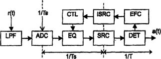
Fig. 1 is the functional block diagram that is presented at the universal asynchronous receiver topology of using in digital transmission and the register system,
Fig. 2 be show asynchronous, based on the functional block diagram of the example of the receiver topology of LMS,
Fig. 3 be show according to asynchronous, based on the functional block diagram of another example of the receiver of the topology of LMS,
Fig. 4 is the functional block diagram that shows according to the receiver topology of the first embodiment of the present invention,
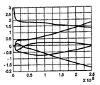
Fig. 5 a and 5b are the figure that shows the simulation result of the receiver that relates separately to Fig. 3 and 4,
Fig. 6 is the figure that shows according to the linear interpolation of the second embodiment of the present invention,
Fig. 7 is the functional block diagram that shows according to the receiver topology of the second embodiment of the present invention,
Fig. 8 a and 8b are the figure that shows the simulation result of the receiver that relates to Fig. 7,
Fig. 9 is the schematic block diagram that shows according to digital display circuit of the present invention.
Detailed description of the Invention
Following commentary relates to label symbol.Identical piece label ordinary representation identical functions entity on all figure.In the back, we also will adopt convention, the underlined symbolic representation of vector, and symbol k and n are the sequences that refers to sampling rate 1/T and 1/Ts respectively.For example, according to this convention, symbol a
kBe meant the sequence of scalars of sampling rate 1/T, and symbol
S nBe meant the vector sequence of sampling rate 1/Ts.The length of vector will be represented that its subscript represents that this symbol is used in vector by symbol N.Therefore, for example, vector
S nLength be represented as N
s
Fig. 1 shows the general topology of the asynchronous band receiver of base that is used for digital transmission and register system.Receiver is from the data sequence a of received signal r (t) generation with data rate 1/T
kReceived signal a
kBe added to simulation low-pass filter LPF, the main function of this wave filter is the inhibition zone external noise.Analog-to-digital converter ADC exports digitizing by, crystal-controlled free-running sampling rate 1/Ts operation asynchronous with data rate 1/T with LPF, and this sampling rate is height and can avoiding confusion enough.The output of ADC is added to balanced device EQ, and this balanced device is used for improving inter symbol interference and noise.Balanced device is by sampling rate 1/Ts operation, that is, 1/T is asynchronous with data rate.Sample rate converter SRC produces synchronous output of equal value, and this output is used as and is used to provide data sequence a
kThe input of bit-detector DET.SRC forms the part of timing recovery loop (TRL), and this TRL does not illustrate on Fig. 1 significantly.Asynchronously on Fig. 1, represent with symbol 1/Ts and 1/T respectively with synchronous clock zone.
In order to overcome the variation of systematic parameter, balanced device EQ usually needs self-adaptation.For this reason, form circuit FEC by error and extract control information from bit-detector DET, this control information is used for via control module CTL control (renewal) equalizer tap.This forms the adaptive loop (EAL) of balanced device.Error is formed in synchronous (1/T) clock zone and occurs, and control must be carried out in asynchronous (1/Ts) territory.Betwixt, need contrary sample rate converter ISRC.In fact, balanced device usually is to have the Ts tap tapped delay line (finite impulse response filter) at interval of second.
Existing asynchronous adaptive technique is based on LMS (lowest mean square) algorithm.By LMS, tap sequence and suitable error sequence are carried out simple crosscorrelation, draw the lastest imformation that is used for equalizer tap.In order to make it possible, tap signal and error signal need be all synchronous on sampling rate and phase place.First condition satisfies via ISRC.Total hysteresis of second conditional request: SRC, bit-detector, error formation circuit and ISRC was mated by the tap signal of correspondingly delaying time before simple crosscorrelation.ISRC and time-delay coupling increase the complicacy of solution.And because the time variation of the hysteresis of SRC and ISRC, the time-delay coupling may out of true.As a result, Adapter Property can worsen.
Fig. 2 shows the example of the receiver that comprises the self-adaptation topology that overcomes above-mentioned shortcoming.The part of Fig. 2 on video data receiver, that is, and with the adaptive relevant part of digital equalizer.Particularly, do not show the timing recovery subsystem of receiver, it controls sample rate converter SRC and temporal interpolation device TI.Receiver comprises adaptive equalizer EQ, a pair of sample rate converter SRC1 and SRC2 and detecting device DET, from the list entries r that receives
nProduce data sequence a
kDetecting device DET is the part of error maker 21, and this error maker is created on the error sequence e that uses the control loop of balanced device from the bit decision that is produced by bit-detector
kThe adaptive LMS technology that is based on of balanced device, this LMS technology for example is at J.W.M.Bergmans, " Digital Baseband Transmission and Recording (digital baseband transmission and record) ", Kluwer Academic Publishers publishes, Boston, 1996, be expressed as and describe in [ref.].The central idea of these technology is, the tap lastest imformation is by with tap signal (the sequence r that receives
n) carry out relevant with error signal and produce.The sum of errors tap signal should have identical sampling rate, and should be phase locked; Any hysteresis in the error signal should be mated by correspondingly delaying time tap signal.
On Fig. 2, r
nThe sequence of expression by sampling and for example obtain periodically from the emulated for playback signal that writes down channel.Sampling is carried out with the free oscillation clock rate 1/Ts that is not equal to data rate 1/T usually.Sequence r
nBe sent to and have Ts tap w at interval
nBalanced device EQ, be used for producing balanced sequences y at output
nPreferably, balanced device EQ is FIR (finite impulse response (FIR)) transversal filter, but it can be any balanced device that comprises linear combiner.The purposes of balanced device is that the response of (for example record) channel is configured as the target response of regulation and regulates noise spectrum.The back of balanced device EQ is sample rate converter SRC1, and it is the sequences y of Ts equilibrium at interval
nBe transformed into the T sequence x at interval of the equivalence of the input end that is supplied to the error maker 21 that comprises bit-detector DET
kT list entries x at interval
kIdeally with channel data sequence a
k Data rate 1/T synchronous.In fact, bit-detector DET produces channel bit a
kValuation
Suppose that bit-detector produces correct judgement, then data sequence a
kWith its valuation
Be identical.So on all figure, the output of bit-detector is represented as a
kBit error once in a while can not influence the performance of system greatly.Alternatively, in the transmission beginning, predetermined sequence of data (usually being called preface) can be placed on before the actual data, so that carry out initial adaptation according to the duplicate of this predetermined sequence of data, this duplicate can be local synchronous in data receiver, and without any error code.Common practice is to carry out the adaptive of starting stage under this so-called " data-aided " mode of operation, and in case adaptive loop convergence just switches to " decision-directed " mode of operation shown in Figure 2.Though obviously do not illustrate on Fig. 2, should see that this explanation also is related to this " data-aided " mode of operation.
The remainder of Fig. 2 shows the mechanism of control loop, is used to use the LMS technology to upgrade the equalizer tap coefficient vector sequence adaptively
W nThe all numeral operations that comprise in control loop for example can be carried out suitable computer program by microprocessor and realize.Double-lined arrow between square represents that vector signal transmits, and single arrow is represented invariant signal.So control loop (balanced device adaptive) comprising:
-the second sample rate converter SRC2 is used for the sequence r that receives
nThe version of time-delay be transformed into intermediate control sequence I with data rate 1/T
k, this 2nd SRC is represented as SRC2, and is preferably identical with a SRC1,
-control information generation device 22 is used for from error sequence e
kWith intermediate control sequence i
kDraw synchronous control vector sequence with data rate 1/T
Z k, and
-the time is inserted device TI, is used for from described synchronous control vector sequence
Z kDraw the control vector sequence
S n
On Fig. 2, the control vector sequence
S nDirectly control balanced device, that is, and the equalizer tap vector sequence
W nOnly with
S nConsistent.Synchronous control vector sequence by the generation of control information generation device
Z kFormed by Nz integrator group 22, its input is from crossed product 24e
k I kDraw, wherein
I kIt is the middle vector sequence that comprises Ni intermediate sequence.All vector lengths equate.So Nz=Ni=2M+1, number 2M+1 are the tap number w among the balanced device EQ
nVector sequence in the middle of this
I kBe sequence r from receiving
nDraw.Predetermined time-delay τ is added to the sequence r that receives
nCarry out serial-to-parallel conversion so that from middle sequence i at shift register SR
kVector sequence in the middle of forming
I kBefore, the version of the time-delay of the sequence that receives is provided to sample rate converter SRC2, so that form intermediate sequence i
k
Therefore the input of balanced device is transformed data rate domain after it is delayed time a predetermined time-delay.Predetermined time-delay does not change in time and knows.It equals the amount of delay that is input to output from balanced device.In case two signals, that is, the signal at the output of each sample rate converter all is in data rate domain, then can easily calculate equalizer coefficients and upgrade.Describe adaptation scheme below in detail.At the variable of the output of integrator 22, with z
k jExpression, obey following equation:
z
k+1 j=z
k j+μΔ
k j,j:-M,...,M (1)
Wherein:
z
k jBe of the output of j integrator at moment k,
μ is a little zoom factor (usually being called step-length) of determining the closed loop time constant,
Δ
k jBe tap error estimator when iteration k, and
2M+1 is the tap number of balanced device.
According to the LMS scheme, the valuation Δ
k jBe given:
Δ
k j=e
k.i
k-j,j:-M,...,M (2)
Wherein:
e
kBe at SRC output and the detecting device input d that wants
k=(a
k* g
k) error between the version of time-delay (), wherein:
g
k, be used for (wave filter G's) target response of equalizer adaptation,
i
K-jBe the sequence r that receives that is transformed into data rate 1/T
nThe version of time-delay.
For the purpose of integrality, should be mentioned that formula (2) and Fig. 2 only describe from error sequence e
kWith list entries r
nDraw tap error estimator Δ
k jOne of various possible mode.For example, two sequence e
kAnd r
nCan firmly quantize, so that simplified embodiment, and the multiplication in (2) formula can be by selectively update mechanism is alternative.
Fig. 2 shows, be updated (synchronization field) second at the every T of synchro control vector sequence Zk of the output of integrator, and equalizer coefficients vector Wn needs every Ts to be updated second, because balanced device moves in asynchronous domain.Carry out base conversion when necessary by temporal interpolation device TI, be used for drawing asynchronous control vector sequence with sampling rate 1/Ts from synchro control vector sequence Zk at the output of integrator group.Because values of tap only changes lentamente with respect to two sampling rates, temporal interpolation can be finished in the simplest mode of imagining, for example by carrying out the bank of latches of zeroth order interpolation, when Ts departs from T when too many, cause additional problem, this needs additional function, is called as spatial interpolation. and additional function is described with reference to Fig. 3.
The tap that balanced device has Ts second at interval, that is, it is used for obtaining tap signal in succession with the Ts step-length time-delay list entries of second, these signals then with by the coefficient vector sequence
W nThe weight w of regulation
n j, j:-M ..., M linear combination.Yet, at the control vector sequence of the output of integrator group
s nBe related to T balanced device at interval, that is,
s nComponent s in succession
jJ:-M, ..., M is meant the weighting factor of the balanced device that is used to have the tap interval T on principle. the steady state solution of arranging according to balanced device and according to the deterioration of loop efficient, the nominal tap of this T second at interval and the difference between the actual tap at interval of Ts second cause the deterioration of Adapter Property. the result, the topology of Fig. 2 mainly is suitable near synchronous application, and for example wherein 1/Ts and 1/T are near each other and preferably differ less than about 20s
-1Application. this condition for example being used for most of channel IC (integrated circuit) of hard disk drive (CD storage), satisfies in the system of many reality.
In order in bigger range of application, to use the present invention, in the improvement project of the scheme that proposes on Fig. 3 on Fig. 2, to describe.According to this improvement project, control loop also comprises the spatial alternation device, is used for from the asynchronous control vector sequence at the output of temporal interpolation device
S nDraw the equalizer coefficients vector
W nAs a result, the initial T sequence at interval that generates in control loop is transformed into and is used to control the equalizer coefficients vector
W nThe Ts sequence at interval of equivalence.On Fig. 3, these spatial alternation devices are represented with symbol SI.Because new variables s more
n jDescribe the coefficient of T balanced device at interval, must become Ts information at interval to this T information conversion at interval really.This makes must be to coefficient s
jCarry out interpolation, this is carried out by spatial interpolator piece SI.Conceptually, new variables s more
jBe the T interval samples of continuous equalization filter of basic time, these impulse responses are represented as w (t), that is, and and s
j=w (jT), j:-M ..., M. hypothesis w (t) is available, we must be at position t
i=i * Ts, i:-M ..., M locates it is carried out resampling, so that generate necessary equalizer coefficients w
i=w (i * Ts).Variable t is express time not here, but the expression position, and hypothesis is a successive value after (span of wave filter) from certain at interval.With identical meaning, i is and irrelevant location index of time number, that is, and and t
iYet determine by i fully and not change in time. because the T interval samples of w (t) is provided only, that is, and s
j, the interpolation of these samples must be used for producing Ts variable w at interval
i
One of the simplest form of interpolation is linear interpolation, and it it seems it is attractive from computed view point, but can consider other interpolation forms, such as, for example or even simpler hithermost contiguous interpolation.The resampling position, t
i=i * Ts can be written as t of equal valuely
i=(m
i+ c
i) T 0≤c wherein
i<1, and
Because c
iBetween 0 and 1, change, so t
iAt m
iT and (m
i+ 1) change between the T, and w (t) is at w (m
iT)=s
m iWith
Between change. according to a kind of linear interpolation method, at position t
iThe numerical value of the w (t) at place is calculated as then:
By means of (4), the spatial interpolator SI of Fig. 3 T spaced tap s at the output of latch
jBe transformed into the Ts spaced tap value of the setting w that represents equalizer tap
i. in order to carry out this conversion, must know or estimate as ratio Ts/T formula (3) expression, channel bit rate and sampling rate.Yet, the valuation of this ratio be in the sample rate converter SRC1 of Fig. 3 available .SRC resampling at moment t
kTs intervening sequence y during=kT
n, it can be written as t again
k=(m
k+ μ
k) Ts.
When having phase error, the difference between sampling instant in succession from the nominal value of T according to t
k-t
K-1=T+ τ
kT changes, wherein τ
kIt is the phase error in the T that rebuilds clock at interval.Then, we obtain following formula:
So to force the mean value of phase error be 0. to the timing recovery loop of control SRC1, the mean value of the amount on the left side of formula (5) will be set in the numerical value of the reality of T/Ts, or the inverse of this ratio that needs for linear interpolation.
" quadrature " control function for the adaptive loop of realizing sequential control loop or PLL and balanced device, need find the solution for the adaptive equalizer of Fig. 3. the time shift that in the impulse response of the FIR wave filter (finite impulse response filter) of balanced device (EQ), occurs as the skew (offset) in " group delay ", by the timing recovery loop full remuneration. the derivative of the phase propetry of " group delay " expression wave filter.As a result, error e
kParticipant causes the skew of the group delay of dispersing irrelevant.For fear of the interference between the adaptive loop of timing recovery and balanced device, the impulse response of adaptive balanced device must not comprise the linear phase term of frequency v, and this is called the quadrature functional conditions.In fact, PLL should only be responsible for proofreading and correct the linear phase term distortion, and adaptive equalizer is responsible for proofreading and correct the phase distortion of all high-orders, for example in the light storage system, for the v that defocuses item
2, for tilting or the v of coma aberration item
3, for because the v of the residue spherical aberration item that causes of the low frequency variations of cover thickness for example
4
Have the asynchronous balanced device based on the LMS expansion of orthogonal control function, novel and come adaptive balanced device, as long as the words that above defined terms satisfies in each adaptation step according to the balanced device control algolithm of LMS type.Receiver according to the first embodiment of the present invention is shown in Fig. 4. in the topology of Fig. 4, we suppose Ts no better than T. represent with identical letter character with Fig. 2 and 3 identical functions entities.New receiver comprises the orthogonal control functional device, draws in order to reduce the interference between two loops, the condition that balanced device should be obeyed. balanced device should be adapted to and make condition always correct.
The derivation of explained later quadrature functional conditions. we are with W (the transport function w that v) represents the FIR wave filter
k:

Phase (linear term that v) must not comprise v, the group delay skew must be deferred to:

And we know, because equalizer coefficients w
kBe real number, for A (v), we have:
A(-v)=A(v)
Therefore also have:
Because

Making up these formula draws:
It is equivalent to:
Keep not having the wave filter of linear phase term should have the tap w that defers to this constraint condition
kFor prevent the equalizer adaptation loop and regularly recover between interference, the object of filter adaptation algorithm must change, and makes square error power J minimum, wherein E[x] mathematical expectation of expression statistical variable x:
Be subject to subsidiary condition:
This causes new cost function (by the adaptive discriminant that is minimized, being called as cost function), wherein
 Be meant:
Wherein λ is the Lagrange multiplication factor. this multiplication factor must be selected such that
 As filter tap w
pFunction be minimized:
As filter tap w
pFunction be minimized:
Or
For definite λ,
 In energy must be minimized:
Draw:
Wherein
 Representative is for a
kDecision value.
Representative is for a
kDecision value.
The now necessary solving equation of equalizer adaptation loop:
Iteratively, by using steepest descent method:
Draw:
It seems that from the viewpoint of reality it is incalculable that steepest descent above-mentioned is upgraded: this expectation instruction need be carried out average computation on the very long time interval.So this gradient substitutes with instantaneous gradient, this provides:
The LMS algorithm of this change will make average square error power minimum. without power, the average absolute value that can seek error minimizes:
Cause new symbolic algorithm:
With sign (e
k) multiplication include only putting upside down of sign, therefore quite simple. as clearly check, should estimate for regularly recovering and the condition of the orthogonal control function of equalizer adaptation loop:
For this algorithm:
Increment is obeyed condition really:
Can carry out identical check for symbolic algorithm, draw similar result.
Fig. 5 shows the simulation result of the gradient of equalizer coefficients to the time.Fig. 5 a shows that result that the topology for Fig. 3 obtains and Fig. 5 b show the result that the topology for Fig. 4 obtains, and comprise the orthogonal control function.Comparison shows that the importance of the orthogonal control function of implementing on Fig. 4 between two figure.In these emulation, used 5 tap adaptive equalizers, and the gradient of 2%. Fig. 5 a and 5 filter taps of 5b demonstration is departed from the Ts territory with respect to data rate domain. on Fig. 5 a,, make tap disperse for the not compensation of quadrature function.On the other hand, on Fig. 5 b, adopt the topology of Fig. 4, make equalizer tap restrain.
Solve another problem in the topology relevant second embodiment of the present invention, Fig. 6 now, be and the diverse situation of T even this second embodiment can be applicable to Ts.Filter update produces in data rate domain, yet this is meant the balanced device at interval for T., this wave filter is the Ts interval.Therefore this topology mainly is for being useful near synchronous application, and wherein to be different from T not many for Ts.
Conceptually, the T spaced filters of calculating is upgraded need be transformed the Ts territory, must carry out interpolation.Fig. 3 and its relevant explanation provide the details of spatial interpolator SI. and this interpolater is carried out message interpolation, and this it seems it is very attractive from the viewpoint of calculating.
Resampling position t
i=iT
sCan be written as t
i=(m
i+ c
i) T, wherein 0≤c
i≤ 1 and
Because c
iBetween 0 and 1, change, so t
iAt m
iT and (m
i+ 1) change between the T, and w is at w (m
iT) with w ((m
i+ 1) change T).
According to linear interpolation shown in Figure 6, we obtain:
W(iT
s)=(1-c
i).w(m
iT)+c
i.w((m
i+1)T)
From basic LMS algorithm:
The application space interpolater:
Cause

Time shift in the impulse response of this new FIR is by regularly recovering full remuneration. result, error e
kParticipant causes the skew of the group delay of dispersing irrelevant. in order to obtain regularly recovering and the orthogonal control function of the adaptive loop of balanced device, must be included in the result who drew in the former explanation for Fig. 4.
This causes the topology of Fig. 7.
If spatial interpolator is applied to the version with " upgrading " extraneous term, the LMS algorithm of being used for the quadrature function, then the adaptive loop of balanced device still has stability problem. asynchronous FIR wave filter is not deferred to condition:
This is because when having at least 5 equalizer tap time space interpolaters not keep this specific character. people are the intuition this point simply, for example, can have for 5 tap filters:

For the notion of the necessity of the interpolater that has living space, carry out DVR emulation with ideal signal.In the DVR photoreceiver, ratio T/Ts is taken as 4/3, causes adaptive equalizer to have the interval of (3/4) T.
Fig. 8 shows the simulation result of the evolution of FIR coefficient to the time. Fig. 8 a shows the result that the topology for Fig. 7 obtains. on Fig. 8 b, do not have spatial interpolator: the T spaced tap upgrade without any conversion be connected to the 3/4T spaced equalizers. this causes tap to disperse. on the other hand, on Fig. 8 a, adopt the topology of Fig. 7, this makes equalizer convergence.
Fig. 9 shows the example according to system of the present invention, comprises the receiver shown in Fig. 2,3,4 and 7.This system for example can be a digital recording system. it comprises register 41, is used for Serial No. 93 is recorded in record carrier 92 and receiver 94, and being used for from sequence 95. record carriers 92 of institute's speed recording carrier playback record for example can be CD.
The interference, the glitch-free asynchronous balanced topology based on lowest mean square that are used for preventing between the adaptive loop of timing recovery loop and balanced device have been described. because the time shift that occurs as the skew of group delay in the impulse response of FIR wave filter drives this error e of the adaptive loop of wave filter by regularly recovering full remuneration
k, participant causes the skew of the group delay of dispersing irrelevant.
Described and how can avoid asynchronous based on the interference between the adaptive loop in the balanced device of LMS.At first draw the condition that the asynchronous adaptive equalizer with orthogonal control function is provided.Subsequently, this constraint condition being incorporated into the lowest mean square criterion that adopts the Lagrange multiplication factor. this has caused offseting the topology of the interference between the adaptive loop. and last, this new structure is extended to has spatial interpolator, so that have greater flexibility for T/Ts ratio.
Though the present invention above be to describe for Fig. 4 and specific asynchronous receiver topology shown in Figure 7 as an example based on LMS, but this does not limit the scope of the invention. ultimate principle of the present invention, be called as " orthogonal control function ", also can be applicable to have any asynchronous receiver topology of the adaptive loop of timing recovery loop and adaptive equalizer based on LMS. ultimate principle of the present invention is the solution that is used to avoid the interference between the adaptive loop of timing recovery loop and balanced device, and wherein balanced device is set in the asynchronous domain.This solution with reference to Fig. 4 and Fig. 7 description, be to calculate in this example for control based on LMS, but in fact also can force control to calculate for zero. solution comprises the change adaptation algorithm, so that satisfy the condition of the noiseless work of system.
Accompanying drawing that provides before this and their explanation are to show rather than restriction the present invention. it will be appreciated that have many alternatives to belong in the scope of claims.In this respect, make the commentary of following ending.Can have and manyly implement the method for function by means of hardware or software item or the two.In this respect, accompanying drawing illustrates that very each only represents a possible embodiment of the present invention.Therefore, though accompanying drawing shows different functions with different piece, this never gets rid of single hardware or the practicable several functions of software item, or function can be carried out by hardware or software item or the subassembly of the two.
Claims (6)
1. be used for from with the sequence (r that receives of the asynchronous clock rate 1/Ts of data rate 1/T sampling
n) in data rate is provided is the data sequence (a of 1/T
k) receiver, receiver comprises:
-adaptive equalizer (EQ) is used for the sequence (r that receives from described
n) in balanced sequence (y is provided
n), described balanced device is operated under the clock rate 1/Ts, and is controlled via the adaptive loop of balanced device,
-sample rate converter (SRC1) is used for the sequence (y described equilibrium
n) be transformed into list entries (x of equal value
k), so that supply with error maker (21) with data rate 1/T via timing recovery loop,
-error maker (21) is used for from described list entries (x
k) in the data sequence (a that will use in two loops is provided
k) and error sequence (e
k),
-orthogonal control functional device (40), be used for adaptive equalizer (EQ) is applied a condition, this condition is: the skew in the group delay should not occur, make the adaptive loop of balanced device proofread and correct the nonlinear phase distortion specially like this, and timing recovery loop is proofreaied and correct linear phase distortion.
2. the receiver as requiring in the claim 1, wherein the adaptive loop of balanced device also comprises spatial alternation device (SI), is used for initial T intervening sequence that generate in the adaptive loop of balanced device, given is transformed into the Ts sequence at interval of the equivalence that is used to control this adaptive equalizer (EQ).
3. as the receiver of requirement in the claim 2, wherein said spatial alternation device (SI) is arranged to carry out linear interpolation.
4. as the receiver of requirement in the claim 2, wherein said spatial alternation device (SI) is arranged to carry out immediate contiguous interpolation.
5. digital display circuit comprises being used for supporting the transmitter that sends Serial No. and being used for supporting the receiver that extracts described Serial No. from described channel by channel, and wherein said receiver is the receiver as requiring in each of claim 1 to 4.
6. in comprising the receiver of adaptive equalizer, a kind of reception is with the sequence (r of clock rate 1/Ts sampling
n) and data rate is provided is the data sequence (a of 1/T
k) equalizer adaptation method, this method may further comprise the steps:
-adaptive equalization step is from the sequence (r that receives
n) in balanced sequence (y is provided
n), described adaptive equalization step is operated under the clock rate 1/Ts, and controls via the adaptive loop of balanced device,
-the first sample-rate-conversion step (SRC1) is the sequence (y of described equilibrium
n) data rate via timing recovery loop that is transformed into an equivalence is the list entries (x of 1/T
k), the list entries (x that this is of equal value
k) will handle by an error generation step (21),
-error generates step (21), from described list entries (x
k) generate the data rate that will in two loops, use data sequence (a as 1/T
k) and error sequence (e
k),
-orthogonal control step (40), be used for the adaptive equalization step is applied a condition, this condition is: the skew in the group delay should not occur, make the adaptive loop of balanced device proofread and correct the nonlinear phase distortion specially like this, and timing recovery loop is proofreaied and correct linear phase distortion.
Applications Claiming Priority (2)
| Application Number | Priority Date | Filing Date | Title |
|---|---|---|---|
| EP02291027.7 | 2002-04-23 | ||
| EP02291027 | 2002-04-23 |
Publications (2)
| Publication Number | Publication Date |
|---|---|
| CN1647197A CN1647197A (en) | 2005-07-27 |
| CN100423120C true CN100423120C (en) | 2008-10-01 |
Family
ID=29266014
Family Applications (1)
| Application Number | Title | Priority Date | Filing Date |
|---|---|---|---|
| CNB038091305A Expired - Fee Related CN100423120C (en) | 2002-04-23 | 2003-04-15 | Interference-free lms-based adaptive asynchronous receiver |
Country Status (7)
| Country | Link |
|---|---|
| US (1) | US7145945B2 (en) |
| EP (1) | EP1502375A2 (en) |
| JP (1) | JP4533740B2 (en) |
| KR (1) | KR100957181B1 (en) |
| CN (1) | CN100423120C (en) |
| AU (1) | AU2003216690A1 (en) |
| WO (1) | WO2003092201A2 (en) |
Families Citing this family (4)
| Publication number | Priority date | Publication date | Assignee | Title |
|---|---|---|---|---|
| DE10334064B3 (en) * | 2003-07-25 | 2005-04-14 | Infineon Technologies Ag | Method and circuit arrangement for calibrating a sampling control signal of a sampling phase selection element which influences the sampling instant of a received signal |
| US7447262B2 (en) * | 2005-05-12 | 2008-11-04 | Rdc Semiconductor Co., Ltd. | Adaptive blind start-up receiver architecture with fractional baud rate sampling for full-duplex multi-level PAM systems |
| US8077765B1 (en) * | 2007-08-15 | 2011-12-13 | Marvell International Ltd. | Mixed minimum mean square error/zero-forcing FIR filter adaptation |
| EP2198427A4 (en) * | 2007-12-21 | 2013-11-06 | Lsi Corp | Systems and methods for adaptive equalization in recording channels |
Citations (3)
| Publication number | Priority date | Publication date | Assignee | Title |
|---|---|---|---|---|
| US5297184A (en) * | 1993-02-01 | 1994-03-22 | Cirrus Logic, Inc. | Gain control circuit for synchronous waveform sampling |
| US5359631A (en) * | 1992-09-30 | 1994-10-25 | Cirrus Logic, Inc. | Timing recovery circuit for synchronous waveform sampling |
| EP0805448A2 (en) * | 1996-04-30 | 1997-11-05 | Cirrus Logic, Inc. | Gain and phase constrained adaptive equalizing filter in a sampled amplitude read channel for magnetic recording |
Family Cites Families (12)
| Publication number | Priority date | Publication date | Assignee | Title |
|---|---|---|---|---|
| JP3224555B2 (en) * | 1990-07-31 | 2001-10-29 | 株式会社リコー | modem |
| BE1007229A3 (en) * | 1993-06-23 | 1995-04-25 | Philips Electronics Nv | TRANSMISSION WITH IMPROVED equalizer. |
| US5751766A (en) * | 1995-04-27 | 1998-05-12 | Applied Signal Technology, Inc. | Non-invasive digital communications test system |
| US5838744A (en) * | 1996-10-22 | 1998-11-17 | Talx Corporation | High speed modem and method having jitter-free timing recovery |
| JPH11239083A (en) * | 1998-02-20 | 1999-08-31 | Sharp Corp | Qam demodulator |
| US6381085B1 (en) * | 1999-07-12 | 2002-04-30 | Cirrus Logic, Inc. | Zero forcing adaptive equalization in a disk drive read channel |
| JP2001053650A (en) * | 1999-08-06 | 2001-02-23 | Fujitsu Ltd | Semiconductor device |
| US6418101B1 (en) | 1999-09-03 | 2002-07-09 | Zen Research (Ireland), Ltd. | Digital read channel for optical disk reader |
| JP2001184795A (en) * | 1999-12-24 | 2001-07-06 | Nec Corp | Information detecting circuit with built-in adaptive equalizer and optical disk device using the same |
| US6975689B1 (en) * | 2000-03-30 | 2005-12-13 | Mcdonald James Douglas | Digital modulation signal receiver with adaptive channel equalization employing discrete fourier transforms |
| US6912258B2 (en) * | 2000-07-07 | 2005-06-28 | Koninklijke Philips Electtronics N.V. | Frequency-domain equalizer for terrestrial digital TV reception |
| US20050002474A1 (en) * | 2003-01-27 | 2005-01-06 | Limberg Allen Leroy | PAM radio signal receiver with phase-tracker succeeding adaptive FIR filtering and preceding adaptive IIR filtering |
-
2003
- 2003-04-15 CN CNB038091305A patent/CN100423120C/en not_active Expired - Fee Related
- 2003-04-15 EP EP03712601A patent/EP1502375A2/en not_active Withdrawn
- 2003-04-15 JP JP2004500439A patent/JP4533740B2/en not_active Expired - Fee Related
- 2003-04-15 WO PCT/IB2003/001605 patent/WO2003092201A2/en active Application Filing
- 2003-04-15 US US10/511,808 patent/US7145945B2/en not_active Expired - Fee Related
- 2003-04-15 KR KR1020047017116A patent/KR100957181B1/en not_active IP Right Cessation
- 2003-04-15 AU AU2003216690A patent/AU2003216690A1/en not_active Abandoned
Patent Citations (3)
| Publication number | Priority date | Publication date | Assignee | Title |
|---|---|---|---|---|
| US5359631A (en) * | 1992-09-30 | 1994-10-25 | Cirrus Logic, Inc. | Timing recovery circuit for synchronous waveform sampling |
| US5297184A (en) * | 1993-02-01 | 1994-03-22 | Cirrus Logic, Inc. | Gain control circuit for synchronous waveform sampling |
| EP0805448A2 (en) * | 1996-04-30 | 1997-11-05 | Cirrus Logic, Inc. | Gain and phase constrained adaptive equalizing filter in a sampled amplitude read channel for magnetic recording |
Also Published As
| Publication number | Publication date |
|---|---|
| CN1647197A (en) | 2005-07-27 |
| AU2003216690A8 (en) | 2003-11-10 |
| JP4533740B2 (en) | 2010-09-01 |
| KR100957181B1 (en) | 2010-05-11 |
| WO2003092201A2 (en) | 2003-11-06 |
| US20050175128A1 (en) | 2005-08-11 |
| US7145945B2 (en) | 2006-12-05 |
| WO2003092201A3 (en) | 2004-01-08 |
| EP1502375A2 (en) | 2005-02-02 |
| KR20040097390A (en) | 2004-11-17 |
| JP2005524279A (en) | 2005-08-11 |
| AU2003216690A1 (en) | 2003-11-10 |
Similar Documents
| Publication | Publication Date | Title |
|---|---|---|
| CN100477652C (en) | Adaptive equalizer operating at a sampling rate asynchronous to the data rate | |
| CN100459604C (en) | ZF-based adaptive asynchronous receiver | |
| US8175201B2 (en) | Systems and methods for adaptive equalization in recording channels | |
| US7054088B2 (en) | Information recording and reproducing apparatus and method, and signal decoding circuit for performing timing recovery | |
| JP4821264B2 (en) | Synchronization device, synchronization method, synchronization program, and data reproduction device | |
| JP3767238B2 (en) | Signal processing device | |
| US20060256896A1 (en) | Robust maximum-likelihood based timing recovery | |
| KR970071696A (en) | Adaptive Equalization and Interpolated Time Recovery in Sample Amplitude Read Channels for Magnetic Recording | |
| CN101310495A (en) | Near-minimum bit-error rate equalizer adaptation | |
| TW200830744A (en) | Electronic dispersion compensation utilizing interleaved architecture and channel identification for assisting timing recovery | |
| CN101223727A (en) | Data - dependent noise predictor in data-aided timing recovery | |
| CN100423120C (en) | Interference-free lms-based adaptive asynchronous receiver | |
| CN101179305B (en) | System and method for electronic dispersion compensation | |
| JPH09167448A (en) | Method and apparatus for data detection of data storage equipment | |
| US20040057268A1 (en) | Data reproduction device | |
| Lin et al. | Characterization with embedded synchronization for read-write channels | |
| Venkataramani et al. | MAP-based timing recovery for magnetic recording |
Legal Events
| Date | Code | Title | Description |
|---|---|---|---|
| C06 | Publication | ||
| PB01 | Publication | ||
| C10 | Entry into substantive examination | ||
| SE01 | Entry into force of request for substantive examination | ||
| C14 | Grant of patent or utility model | ||
| GR01 | Patent grant | ||
| C17 | Cessation of patent right | ||
| CF01 | Termination of patent right due to non-payment of annual fee |
Granted publication date: 20081001 Termination date: 20120415 |