CN100412603C - Projection TV with improved micromirror array - Google Patents
Projection TV with improved micromirror array Download PDFInfo
- Publication number
- CN100412603C CN100412603C CNB2004100546587A CN200410054658A CN100412603C CN 100412603 C CN100412603 C CN 100412603C CN B2004100546587 A CNB2004100546587 A CN B2004100546587A CN 200410054658 A CN200410054658 A CN 200410054658A CN 100412603 C CN100412603 C CN 100412603C
- Authority
- CN
- China
- Prior art keywords
- micromirror
- projection
- light
- array
- limit
- Prior art date
- Legal status (The legal status is an assumption and is not a legal conclusion. Google has not performed a legal analysis and makes no representation as to the accuracy of the status listed.)
- Expired - Fee Related
Links
Images


Classifications
-
- G—PHYSICS
- G02—OPTICS
- G02B—OPTICAL ELEMENTS, SYSTEMS OR APPARATUS
- G02B26/00—Optical devices or arrangements for the control of light using movable or deformable optical elements
- G02B26/08—Optical devices or arrangements for the control of light using movable or deformable optical elements for controlling the direction of light
- G02B26/0816—Optical devices or arrangements for the control of light using movable or deformable optical elements for controlling the direction of light by means of one or more reflecting elements
- G02B26/0833—Optical devices or arrangements for the control of light using movable or deformable optical elements for controlling the direction of light by means of one or more reflecting elements the reflecting element being a micromechanical device, e.g. a MEMS mirror, DMD
- G02B26/0841—Optical devices or arrangements for the control of light using movable or deformable optical elements for controlling the direction of light by means of one or more reflecting elements the reflecting element being a micromechanical device, e.g. a MEMS mirror, DMD the reflecting element being moved or deformed by electrostatic means
-
- B—PERFORMING OPERATIONS; TRANSPORTING
- B81—MICROSTRUCTURAL TECHNOLOGY
- B81B—MICROSTRUCTURAL DEVICES OR SYSTEMS, e.g. MICROMECHANICAL DEVICES
- B81B7/00—Microstructural systems; Auxiliary parts of microstructural devices or systems
- B81B7/0032—Packages or encapsulation
- B81B7/0067—Packages or encapsulation for controlling the passage of optical signals through the package
-
- G—PHYSICS
- G02—OPTICS
- G02B—OPTICAL ELEMENTS, SYSTEMS OR APPARATUS
- G02B26/00—Optical devices or arrangements for the control of light using movable or deformable optical elements
- G02B26/08—Optical devices or arrangements for the control of light using movable or deformable optical elements for controlling the direction of light
- G02B26/0816—Optical devices or arrangements for the control of light using movable or deformable optical elements for controlling the direction of light by means of one or more reflecting elements
- G02B26/0833—Optical devices or arrangements for the control of light using movable or deformable optical elements for controlling the direction of light by means of one or more reflecting elements the reflecting element being a micromechanical device, e.g. a MEMS mirror, DMD
-
- G—PHYSICS
- G03—PHOTOGRAPHY; CINEMATOGRAPHY; ANALOGOUS TECHNIQUES USING WAVES OTHER THAN OPTICAL WAVES; ELECTROGRAPHY; HOLOGRAPHY
- G03B—APPARATUS OR ARRANGEMENTS FOR TAKING PHOTOGRAPHS OR FOR PROJECTING OR VIEWING THEM; APPARATUS OR ARRANGEMENTS EMPLOYING ANALOGOUS TECHNIQUES USING WAVES OTHER THAN OPTICAL WAVES; ACCESSORIES THEREFOR
- G03B21/00—Projectors or projection-type viewers; Accessories therefor
- G03B21/14—Details
- G03B21/28—Reflectors in projection beam
-
- G—PHYSICS
- G03—PHOTOGRAPHY; CINEMATOGRAPHY; ANALOGOUS TECHNIQUES USING WAVES OTHER THAN OPTICAL WAVES; ELECTROGRAPHY; HOLOGRAPHY
- G03F—PHOTOMECHANICAL PRODUCTION OF TEXTURED OR PATTERNED SURFACES, e.g. FOR PRINTING, FOR PROCESSING OF SEMICONDUCTOR DEVICES; MATERIALS THEREFOR; ORIGINALS THEREFOR; APPARATUS SPECIALLY ADAPTED THEREFOR
- G03F7/00—Photomechanical, e.g. photolithographic, production of textured or patterned surfaces, e.g. printing surfaces; Materials therefor, e.g. comprising photoresists; Apparatus specially adapted therefor
- G03F7/70—Microphotolithographic exposure; Apparatus therefor
- G03F7/70216—Mask projection systems
- G03F7/70283—Mask effects on the imaging process
- G03F7/70291—Addressable masks, e.g. spatial light modulators [SLMs], digital micro-mirror devices [DMDs] or liquid crystal display [LCD] patterning devices
-
- H—ELECTRICITY
- H04—ELECTRIC COMMUNICATION TECHNIQUE
- H04N—PICTORIAL COMMUNICATION, e.g. TELEVISION
- H04N5/00—Details of television systems
- H04N5/74—Projection arrangements for image reproduction, e.g. using eidophor
- H04N5/7416—Projection arrangements for image reproduction, e.g. using eidophor involving the use of a spatial light modulator, e.g. a light valve, controlled by a video signal
- H04N5/7458—Projection arrangements for image reproduction, e.g. using eidophor involving the use of a spatial light modulator, e.g. a light valve, controlled by a video signal the modulator being an array of deformable mirrors, e.g. digital micromirror device [DMD]
-
- B—PERFORMING OPERATIONS; TRANSPORTING
- B81—MICROSTRUCTURAL TECHNOLOGY
- B81B—MICROSTRUCTURAL DEVICES OR SYSTEMS, e.g. MICROMECHANICAL DEVICES
- B81B2203/00—Basic microelectromechanical structures
- B81B2203/03—Static structures
- B81B2203/0369—Static structures characterized by their profile
- B81B2203/0384—Static structures characterized by their profile sloped profile
Abstract
A packaged micromirror array for a projection display according to the application comprises an array of micromirrors that are capable of movement between an OFF state and an ON state by pulse width modulation to achieve a gray scale image on a target and wherein each micromirror corresponds to a pixel in a viewed image on the target; and a package having a light transmissive window. The array of micromirrors is disposed in the package having the light transmissive window. A viewed image, formed on the target by light reflected from the micromirrors and passed through said mask, has four sides and viewed pixels within the image formed by said micromirrors each have four sides which are not parallel to any sides of the viewed image.
Description
The application is for dividing an application, its original application be enter the China national stage on January 30th, 2003, international filing date is the International Patent Application PCT/US01/24332 in August 3 calendar year 2001, the China national application number of this original application is 01813608.7, and denomination of invention is " encapsulation of micromirror element, micromirror element and an optical projection system thereof ".
Technical field
The present invention relates to a kind of projection TV, particularly relate to a kind of forth screen projection or back screen television.
Background technology
The United States Patent (USP) 5 of Huibers, 835, No. 256 and 6,046, No. 840, U.S. Patent application 09/617 with people such as Huibers, 419, the subject content of each patent (application) is bonded to this by reference, and these patents (application) have disclosed the micro electro mechanical device (MEMS) that is used for control bundle, for example in optical switch, and/or be used for display (for example projection display).A common characteristic is transportable micromirror, so that the inclination angle of dependence micromirror element is by different angular deflection light beams.In the type of a kind of visual display system of routine or projection display system, the micromirror element of reflection is used to produce image.Typical micromirror element is a square, and has an independent inclination angle for " opening " state, is straight for " pass " state, perhaps for " opening " state and " pass " state same inclination angle is arranged, but contrary sign is arranged.
Summary of the invention
The invention provides a kind of rear-screen projection or forth screen projection TV, this TV comprises: the screen of light source, micromirror array and the viewed image of demonstration, each micromirror in described micromirror array has by the fixed quadrangle form of the margin of four micromirror.Described TV is in when work, incides on the above-mentioned micromirror array and is directed on this screen with the form of rectangular image from the light of light source; Wherein this micromirror width modulation, thus can move so that on this screen, obtain gray level image opening between state and the off status; And wherein each micromirror is all corresponding to a pixel in this viewed image on this screen; And wherein this viewed image has four edges, and the limit of the pixel in this viewed image is not parallel with the limit of any image.
The present invention also provides another kind of rear-screen projection or forth screen projection TV, and this TV comprises: the screen of light source, micromirror array and the viewed image of demonstration; Wherein incide on this micromirror array from the light of this light source and be directed on this screen as rectangular image in when work: the micromirror width modulation in this micromirror array, thereby can open between state and the off status mobile so that on this screen, obtain gray level image; And wherein each micromirror is all corresponding to a pixel in the viewed image on this screen; And wherein this viewed image has four edges, and wherein each micromirror forms the micromirror image of a correspondence on this screen, this micromirror has the projection of an independent convex on the direction on a limit of the rectangular image on this screen, and this micromirror does not have and real parallel limit, the limit of this rectangular image; The horizontal line of this micromirror wherein according to the row on the one side that is parallel to this rectangular image, and is extended from a corner to another ground, corner, and wherein in each row the perpendicular line corresponding with addressed column extend and be connected to micromirror of each other row from each micromirror; And the vertical row of this micromirror wherein, row according to the one side that is parallel to this rectangular image, and extend from a corner to ground, another corner, and wherein in each row the horizontal line corresponding with addressed row extend and be connected to the micromirror of each other row from each micromirror.
In order to be reduced to minimum along the optical diffraction of switch direction, the optical diffraction that particularly will reach the acceptance cone of collecting optical system (collection optics) is reduced to minimum, in the present invention, use the micromirror (said " rectangle " comprises square micromirror) of non-rectangle here.Here said diffraction is represented the scattering that the light of periodic structure leaves, and wherein light must not be monochromatic or phase coherence.Equally, for the cost of lamp optical system and the size of display unit of the present invention are reduced to minimum, light source is placed with and the row of array (perhaps row) quadrature, and/or light source is placed with one side quadrature with framework, and this framework limits the useful area of array.Though the limit quadrature of incident beam and row (perhaps row) and/or useful area, for the limit quadrature of the single micromirror in the array not necessarily.The limit of quadrature causes the direction diffraction of incident beam along the micromirror switch, and causes light " leakage " to enter into " opening " state, even micromirror is at " pass " state.This optical diffraction has reduced the contrast ratio of micromirror.
The present invention has optimized the contrast ratio of micromirror array, and when " pass " state at them of micromirror, their send minimum light to area of space like this, and this area of space is exactly when the zone of micromirror in their " opening " state time Be Controlled arrival.More particularly, the present invention includes light source and the incident beam and the specially designed micromirror in array of a special location, this micromirror makes the optical diffraction of the acceptance cone that reaches projection (perhaps observation) optical system be reduced to minimum, so that improved contrast ratio is provided.By the wringing fit of considering micromirror and the big activity coefficient (fill factor) that has low diffraction from " pass " state to " opening " state, even when array is thrown light on by the optical axis along the micromirror cycle, arrangement of the present invention and structure are also with the long-pending minimum that is reduced to of the non-reflecting surface in the array.Just, by angled limit not with the rotating shaft parallel of micromirror, this structure optimization contrast ratio, and optimized activity coefficient by hinge (hinge), this hinge needs relatively little area and the non-reflector space that allows adjacent micromirror and minute quantity to be wasted to tilt together.The structure of the micromirror of the various examples of the present invention and shape have also reduced micromirror crosstalking between the neighboring micro sheet during by deflection statically.
Another aspect of the present invention is a micromirror array, and micromirror single in this array tilts around a state straight or non-deflection asymmetricly.Be in an angle by " pass " state that makes micromirror, this angle is littler than the opposite angle in the micromirror of " opening " state, a) from the edge of micromirror and enter the diffraction light of collecting optical system and be reduced to minimum; B) be scattered and enter the light of collecting optical system under the micromirror and also be reduced to minimum; C) stroke of micromirror is reduced, and so the contiguous mutual possibility of collision of micromirror is reduced to minimum, the activity coefficient that this reduces the slit between the micromirror conversely again and increases micromirror; D) angle of micromirror deflection can be added to bigger scope, and it is bigger that this scope is compared to out the scope that micromirror array that state and off status have same deflection angle arranges.
Another aspect of the present invention is the encapsulation of micromirror array, and this encapsulation has the part of a transmissive light, and this part is not parallel to micromirror formation substrate thereon.The part of transmitted light can be any suitable material, glass plate for example, and quartz or polymkeric substance, and consider that guiding is from the direct reflection of the substrate of transmitted light rather than the direct reflection of coming the parallel light transmissive plate in the comfortable encapsulation to cause.Preferably direct reflection is directed into enough away from collecting optical system so that the increase of the size of illumination cone will make direct reflection not enter the collection optical system.
A further aspect of the invention is an optical projection system, comprises an effective micromirror array that is arranged to rectangle, and this micromirror can be rotated around off status and the switch shaft of opening between the state, and micromirror is corresponding to the pixel in the observed image; Comprise a light source that is used for light is directed to micromirror array, this light source is configured to so that direct light is not orthogonal at least two limits of each micromirror, and, when each micromirror is used as vertical view observation, be parallel to the limit of two other at least of each micromirror; Comprise the collection optical system that is arranged to accept from the light of opening the micromirror under the state.
Another aspect of the present invention is an optical projection system, comprises a micromirror array, a pixel in the corresponding observed image of each micromirror, and have the shape of concave polygon or one or more non-rectangle parallelogram; One is used for light is directed to the light source that micromirror array is collected optical system, and this collections optical system is arranged to accept the light that reflects from micromirror.
Another aspect of the present invention remains an optical projection system, comprise a light source that is used to provide incident beam, the array of reflecting element movably, with a collection optical system that is used for projection from the light of array, wherein the projected image from optical projection system will be displayed on the target with rectangular image, this image is made of to millions of pixels thousands of, and the shape of each pixel is the combination of concave polygon, single non-rectangle parallelogram or non-rectangle parallelogram.
Another aspect of the present invention still is an optical projection system, comprise a light source, the array of a removable micromirror element, with the collection optical system, wherein each the micromirror element in the array has a switch shaft, this switch shaft is basically parallel at least one limit of array useful area, and becomes the angle of 35 to 60 degree with one or more limit of micromirror element.
Another aspect of the present invention is an optical projection system, the array that comprises a light source and a removable micromirror element, each micromirror element has the limit (leadingside) of a front, this limit is not orthogonal to incident beam, also be not orthogonal to any limit of useful area, so that its contrast ratio increases by 2 to 10 times with having to compare with the micromirror element on the perpendicular limit of incident beam.
Another aspect of the present invention is an optical projection system, comprises a light source, collects the array of an optical system and a removable micromirror element, and this optical projection system has and the basic the same diffraction pattern (pattern) shown in Figure 21 C.
Another aspect of the present invention remains an optical projection system, the movably micromirror array that comprises a light source and a rectangle, micromirror can move opening between state and the off status, and the light of opening under the state can be reflexed to prescribed space area, wherein light source is arranged to basic an angle of 90 degrees light is directed at least one limit of the rectangle that is limited by array, and wherein, there is not diffraction light to enter into prescribed space area basically when micromirror during in off status.
Another aspect of the present invention is the method that projects image onto on the target, comprise: lead beam is to the micromirror array of rectangle, light beam be directed into the limit of rectangular array front at an angle, this angle is within positive 90 degree add deduct the scopes of 40 degree, and wherein the shape of the micromirror in the array is polygon and is oriented to so that light beam incides on all limits of polygon with the angles that are different from 90 degree; And will from the optical projection of micromirror on target so that form image thereon.
Another part of the present invention is an optical projection system, comprise a light source, light collecting system and a micromirror array, this array is arranged to the light of ground, space modulation from light source, this matrix-like is formed on the substrate and is configured to make each micromirror can be on primary importance when not being activated, each micromirror can move on the open position light is directed to the light collecting system of array, and can move in the opposite direction to close on the position and leave light collecting system with direct light, said open position is all different with said primary importance with the position, pass, and wherein open position with respect to primary importance at an angle, this angle is different from the angle of closing the position.
Another aspect of the present invention is a kind of method that is used for ground, space modulated beam of light, comprise by micromirror array and will be directed to light collecting system from the light beam of light source, this micromirror array is arranged to the light beam of ground, space modulation from light source, this array be formed on the substrate and when not modulating each micromirror be in primary importance, the modulation micromirror makes each micromirror move to open position in array, light is directed to the light collecting system of array in this position, and move to and close the position, leave light collecting system with direct light, said open position and close the position and all be different from said primary importance, and wherein open position is different from the numerical value of the angle when closing the position with respect to primary importance numerical value at an angle.
Another aspect of the present invention still is an optical micromechanical element that is formed on the substrate, this element has open position on the first angle numerical value with respect to substrate, relevant position on the numerical value of second angle on respect to substrate, the first and second numerical value differences, and have the 3rd position that is arranged essentially parallel to substrate, open position and position, pass are all limited by nestling up optical micromechanical element substrate or that nestle up the structure that is formed on the said substrate.
Another aspect of the present invention remains the method that is used for light modulated, but comprises the light of reflection from the deflection micromirror array on the substrate that is disposed in the plane, and said micromirror tilts to primary importance or tilts to the second place; Obviously different in angle that forms between said primary importance and the substrate and the angle that between the said second place and substrate, forms therein.
Another aspect of the present invention is the method that is used for light modulated, comprise a light source, the light modulator arrays on a plane, but this array comprises deflecting element and collects optical system, wherein the element in the array is configured to two states at least selectively, wherein guide light to enter the collection optical system through first angle from light source at first state element, guide light to enter the collection optical system at second state element through second angle from light source, on behalf of light, the third angle degree be reflected from array, as array is the surface of micromirrorization, and wherein the difference of the difference of first angle and third angle degree and second angle and third angle degree is visibly different.
Another aspect of the present invention is an optical projection system, comprises the light source that is used to provide light beam; A micromirror array, this array comprise a plurality of micromirror that are set in this beam path; With collect optical system, this system be arranged in light beam incide on the micromirror array and reflection leave in the array as after most micromirror of opening and closing the micromirror pattern, in the light path of light beam; Wherein micromirror array comprises a substrate, and micromirror array is fixed on the substrate, and each micromirror on substrate can move to open position from the position of non-deflection and close the position, and wherein open position becomes different angles with the position, pass with respect to non-inflection point.
Another part of the present invention still is a kind of method that is used to project image onto target, comprises the light beam from light source is directed on the micromirror array; Modulate each micromirror to open position or position, pass, wherein in open position, the micromirror direct light is to collecting optical system, and this system is arranged for reception light from micromirror when micromirror is in open position, and the pattern of wherein opening and close micromirror forms image; And wherein, the numerical value of the angle that the position of micromirror becomes in the micromirror open position is different with the numerical value of the angle of the position one-tenth that closes micromirror in the position in micromirror.
Another part of the present invention remains the method that is used for the spatial modulation light beam, comprise that lead beam is to micromirror array, micromirror array can move to first or the second place, wherein micromirror is inducted into a part that is mapped to the light beam on it and enters into the collection optical system in primary importance, and wherein the minor increment between the neighboring micro sheet of each micromirror when the second place less than the minor increment between the neighboring micro sheet of each micromirror when the primary importance.
Another aspect of the present invention is a kind of device, comprises a substrate, constitutes a micro-mechanical device reflection or diffraction on the substrate; Be used for fixing the encapsulation of substrate and removable micro-mechanical device; Encapsulation therein comprises the optical transmission window, and this window and substrate are not parallel.
The present invention more another part is an optical projection system, comprises a light source; Light is collected optical system; A substrate constitutes a reflection or diffraction micro-mechanical device on this substrate; Be used for fixing the encapsulation of substrate and removable micro-mechanical device; Wherein encapsulation comprises and the uneven optical transmission window of substrate; Be arranged on micro-mechanical device from the encapsulation in the path of the light beam of light source and be used to modulate light, and collect optical system and collect the light of modulating from this light beam.
The present invention further another part still is a projector (projector), comprise a light source, micro electronmechanical (MEMS) device of an encapsulation, this microelectromechanicdevices devices has a substrate and the window in encapsulation, a micro-mechanical device is arranged on this substrate, this window be configured to substrate at an angle, also comprise the collection optical system, be configured to receive the light of modulating from the packed microelectromechanicdevices devices (MEMS) of light source.
Another aspect of the present invention is a kind of method that is used to make micromirror, and comprising provides a substrate;
Deposition first is sacrificed (sacrificial layer) layer and is made first to sacrifice formation pattern (patterning) on substrate; On sacrifice layer, deposit at least one deck hinge (hinge) layer, and make at least that one deck hinge layer forms pattern to constitute at least one flexible hinge; Deposit second sacrifice layer and make second sacrifice layer form pattern, on second sacrifice layer, deposit one deck mirror plate layers at least, and make at least one deck mirror plate layers form pattern constituting a lens element, and remove first and second sacrifice layers so that discharge micromirror.
Another aspect of the present invention still is the optical micromechanical device still, comprises a substrate; First post on substrate; A flexible hinge, wherein the near-end of this flexible hinge is on this post; Second post that is connected in the far-end of flexible hinge; With a plate that is connected on second post.
Description of drawings
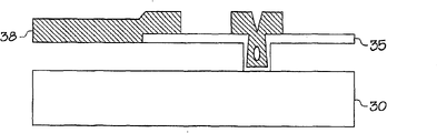
Fig. 1 is the vertical view of an embodiment of micromirror of the present invention;
Fig. 2 A is the viewgraph of cross-section of micromirror to Fig. 2 E, takes from the line 2-2 along Fig. 1, is used to illustrate a kind of method of making micromirror of the present invention;
Fig. 3 A is to be shown in the viewgraph of cross-section of Fig. 2 A to the identical micromirror of Fig. 2 E to 3D, but takes from the line 3-3 along Fig. 1;
Fig. 4 A is the viewgraph of cross-section of micromirror to Fig. 4 J, is used to illustrate the another kind of method of making micromirror of the present invention;
Fig. 5 A is the viewgraph of cross-section of micromirror to Fig. 5 G, is used to illustrate the method for another manufacturing micromirror of the present invention;
Fig. 6 A is the plan view of difform micromirror and hinge combination to 6C;
Fig. 7 is the plan view of a part with micromirror array of micromirror identical among a plurality of and Fig. 6 A;
Fig. 8 is the three-dimensional view that the part of one embodiment of the present of invention is decomposed;
Fig. 9 A is a viewgraph of cross-section to 9C, shows the action of micromirror of the embodiment of Fig. 8;
Figure 10 A is still according to the viewgraph of cross-section of the process of an alternative embodiment of the invention to 10D;
Figure 11 A is a cross-sectional view to 11C, shows the action of the micromirror of making according to the method for illustrating in the 10D at Figure 10 A.
Figure 12 is the plan view of a plurality of micromirror in the micromirror array that constitutes to the method for 11C according to Figure 11 A.
Figure 13 is the three-dimensional view that the part of the micromirror of Figure 12 is decomposed.
Figure 14 A shows the micromirror of " pass " state with smooth non-deflection to 14C.
Figure 15 A shows the micromirror of " opening " and " pass " state of the deflection with equal angles to 15C.
Figure 16 A shows the micromirror of the angle of " opening " state greater than the angle of " pass " state to 16C.
Figure 17 A shows the packaging system of micromirror to 17E, and this packaging system has angled window.
Figure 18 is the illustration of the illuminator of micromirror array of the present invention.
Figure 19 A shows the relation between the limit of the limit of incident light, micromirror and useful area to 19E.
Figure 20 is the instance graph of the micromirror array of prior art.
Figure 21 and Figure 22 are the figure of embodiments of the invention, and the limit of foursquare therein micromirror and useful area at an angle.
Figure 23 shows micromirror to Figure 25, and wherein, " leading edge " and " back edge " of micromirror are not orthogonal to incident beam.
Figure 26 A is the illustration with micromirror of one or more parallelogram shape to 27F to 26F and 27A.
Figure 28 is the illustration of single micromirror.
Figure 29 is the illustration of micromirror array, and this micromirror array has the preceding and back perpendicular to incident beam, also has the another part that becomes miter angle with incident beam.
Figure 30 and 31 is illustrations of micromirror array, and wherein micromirror does not have the limit to be parallel to or perpendicular to the limit of the effective coverage of incident beam and array.
Figure 32 A is the illustration with micromirror of corresponding hinge arrangement to 32J.
Figure 33 A is the illustration of diffraction pattern to 33C, and this diffraction pattern has the diffraction lines by the acceptance cone of collecting optical system (33A), and avoids acceptance cone (33B and 33C).
Embodiment
Be used for little manufacturing movably the method for micromirror or micromirror array be disclosed in the United States Patent (USP) 5,835, No. 256 and 6,046, No. 840 of Huiber, the subject content of each patent is by with reference to being bonded to this.A kind of similar methods that is used for constituting micromirror of the present invention is shown in Fig. 1 to Fig. 3.Fig. 1 is the vertical view of an embodiment of micromirror of the present invention.As in Fig. 1 can see that post 21a and 21b support micromirror plate 24 by hinge 120a on substrate and 120b, this substrate has electrode (not expressing) thereon, electrode is used to cause the deflection of micromirror plate 24.Though do not have shown in Figure 1ly, will be here further to discuss, thousands of even millions of micromirror 24 can be set in the array, is used to reflect incident beam on it and projected image to viewer or target/video screen.
The enough various methods of other micromirror energy in micromirror 24 and the array are manufactured.Wherein a kind of method is shown in Fig. 2 A and (takes from the xsect 2-2 along Fig. 1) in Fig. 2 E, and wherein micromirror preferably is fabricated on the substrate of transmitted light, and this substrate combines with circuitry substrate then.This method further disclosed in the people's such as Llkov that are that on August 30th, 2000 submitted to No. 60/2,292,46, the United States Patent (USP) provisional application and No. 09/7,324,445, the people's such as Llkov that submit on Dec 7th, 2000 U.S. Patent application in.Though this method will be described by the substrate together with transmitted light, any other suitable substrate also can be used, and for example has the Semiconductor substrate of circuit.If Semiconductor substrate for example monocrystalline silicon is used, perhaps preferably the cornice of micromirror is connected to 3 layers of metal in the integrated circuit (IC) process electricly, and uses the material of conduction at least a portion as micromirror.Directly will be discussed in more detail at this in the method that constitutes micromirror on the circuitry substrate (on the transmitted light substrate that replaces separating).
As in Fig. 2 A can see that the substrate 13 of printing opacity (increasing before the layer) is glass (for example Corning 1737F or Eagle2000) for example, quartz, Pyrex at least thereon
TM, sapphire or the like is provided.The substrate of printing opacity can add the photoresistance interlayer of selecting to its bottom to help to handle substrate during processing.Such photoresistance interlayer can be the TiN layer, and this TiN layer is to become the thickness of 2000 dusts to deposit to the back of the substrate of transmitted light by counteractive sputter, will be removed after in a single day this TiN layer machines.Substrate can be Any shape and size, though the shape that is used in the standard wafer in the integrated circuit manufacturing is by preferably.
As in Fig. 2 A can see, sacrifice layer 14, for example amorphous silicon is deposited.Sacrifice layer can be other material that is fit to, can be from micro mechanical structure material (SiO for example after this material
2, polysilicon, polyimide, novolaks or the like) remove down.The thickness range of sacrifice layer is very wide, depends on the size and the needed inclination angle of displaceable element/micromirror, though thickness from 500 dusts to 50000 dusts, preferably about 5000 dusts.Substitute as amorphous silicon, sacrifice layer can be any one of many polymkeric substance, photoresist (photoresist) or other organic materials are (perhaps even polysilicon, silicon nitride, silicon dioxide or the like, depend on selected) to resistive material of etchant and selected etchant.Sticking and the promoting agent of selecting (adhesion promoting) (SiO for example
2Perhaps SiN) can before sacrificial material, be employed.
In order to provide contact area between substrate 13 and the micro mechanical structure layer that deposits later, the hole 6 with width " d " is formed in the sacrifice layer.Form hole by mask with the dissolubility (depending on that resist is positive resist or negative resist) that increases or reduce resist by rotation and direct light on photoresist.The size of size " d " can from 0.2 to 2 micron (preferably approximately being 0.7 micron), depends on the final micromirror and the size of micromirror array.After the development resist was with the resist in the zone of removing the hole, the hole was etched in the amorphous silicon of sacrifice layer by chlorine or other suitable etchant (material that depends on sacrifice).Remaining photoresist is removed then, for example uses the plasma of oxygen.Hole in sacrifice layer can be any suitable dimensions, though preferably have the diameter of from 0.1 to 1.5 μ m, more preferably about 0.7+/-0.25 μ m.Etching is performed until glass/quartz substrate, and perhaps up to any middle layer, for example sticking and promoting agent layer is if the substrate of transmitted light is etched fully, preferably in the quantity less than 2000 dusts.If sacrifice layer 14 is the materials (for example novolaks (novolac) or other photosensitive photoresist) that can directly form pattern, the additional photoresist layer that is deposited so and is developed on the sacrifice layer 14 is unwanted.Under these circumstances, the sacrifice layer of photoresist is formed pattern removing the material in the zone in hole 6, and then before deposition of additional layer by hardening selectively.
In this, as in Fig. 2 B can see that first structural sheet 7 is by for example chemical vapors (vapor) deposition deposition.Preferred this material is by the silicon nitride or the monox of LPCVD (infrabar chemical vapour deposition) or PECVD (chemical vapour deposition that plasma strengthens) deposition, yet any suitable membraneous material is polysilicon for example, metal or metal alloy, silit or organic compound can be deposited over this point (sacrifice layer and etchant should be suitable for employed structured material certainly).The thickness of ground floor can change because of the size of displaceable element and the size of needed element hardness, yet this layer has thickness from 100 dusts to 3200 dusts in one embodiment, more preferably at 900 dusts between 1100 dusts.As in Fig. 2 B can see that layer 7 extends in sacrifice layer in the etched hole.
As in Fig. 2 C can see that the second layer 8 is deposited.Material can identical with the material of ground floor (for example silicon nitride) or different (monox, silit, polysilicons or the like), and can be by as the chemical vapour deposition effect deposition that is used for ground floor.The thickness of the second layer can be bigger or little than ground floor, depends on the needed hardness of displaceable element, the needed flexibility of hinge, employed material or the like.In one embodiment, the thickness of the second layer to 2100 dusts, and preferably approximately is 900 dusts from 50 dusts.In another embodiment, ground floor is deposited by PECVD and the second layer is deposited by LPCVD.
In being shown in the embodiment of Fig. 2 A in the 2E, the ground floor and the second layer all are deposited in the zone that defines removable (micromirror) element and post.According to the conceivable hardness that is used for the micromirror element, any one deck that only deposits in the ground floor or the second layer in the zone of micromirror element also is possible.Similarly, also can be with independent layer replacing 7,8 two-layerly to be used for whole microstructure area, though this can relate to the compromise of the flexibility of the hardness of plate and hinge.Similarly, if an independent layer is used, constitute the flexibility that hinged areas can partly be etched with the hinge that is reduced in the thickness in this zone and improves thereby cause.It also is possible use surpassing two-layer (laminate) displaceable element that produces layering, and this size at displaceable element is increased that for example to be used at optical switch switch light beam be to wish especially.Be used for the such layer or the material of multilayer and also can comprise metal alloy and dielectric substance or metal and nitrogen, oxygen, carbon compound (particularly transition metal).These selectable materials of a part are disclosed in U.S. Patent application 60/228, No. 007, and the subject content of this patent is incorporated into this by reference.
As what can see in Fig. 2 D, a reflection horizon 9 is deposited.Reflecting material can be gold, silver, titanium, aluminium or other metal, perhaps more than a kind of alloy of metal, though the aluminium by the PVD deposition preferably.Metal layer thickness can preferably approximately be 500 dusts from 50 dusts to 2000 dusts.Can add a selectable metal passivation layer, for example a silicon oxide layer that deposits to 10 to 1100 dusts above 9 layers by PECVD.Other metal deposition technique also can be used for depositing metal layers 9, for example chemical liquid deposition and plating.After depositing 9 layers, photoresist is rotated and forms pattern, and then is with suitable metal etchants etch metal layers.Under the situation of aluminium lamination, chlorine (perhaps bromine) chemical substance can be used (for example with for example Ar of the dilution with selectable preferably inertia and/or the Cl of He
2And/or BCl
3(perhaps Cl
2, CCl
4, Br
2, CBr
4Or the like) plasma/RIE etching).Should not need to be deposited at last by the attention reflex layer, but more suitable can directly being deposited on the sacrifice layer 14 forming between other layer of micromirror element, perhaps as the unique layer that forms the micromirror element.Yet, in certain methods,, perhaps need dielectric layer deposition depositing metal layers afterwards because dielectric is deposited under higher temperature.
Relate to Fig. 2 E, the ground floor and the second layer 7,8 are can be after the reflection horizon etched with the combination of known etchant or etchant (the isotropic grade that depends on employed metal and needs).For example, the ground floor and the second layer can (for example be used F with chlorine chemistry or fluorine chemistry (perhaps other halogenide)
2, CF
4, CHF
3, C
3F
8, CH
2F
2, C
2F
6, SF
6Or the like plasma/RIE etching, the combination of perhaps more similar above-mentioned or additional gas, for example CF
4/ H
2, SF
6/ Cl
2Perhaps use the gas that surpasses a kind of etch species, for example CF
2Cl
2, all may all have one or more and can select the inertia dilution) etching.Certainly, if different materials is used for the ground floor and the second layer, use different etchants to come each layer of etching (the plasma etching chemistry that is known in the art according to employed material) so.If the reflection horizon was deposited before the ground floor and the second layer, employed etching chemistry should be reversed.Perhaps, depend on employed material, all layers can be by etching together.The slit 20a with width " e " and the 20b that are shown in Fig. 2 E are used for post 21 and micro mirror lamellar body 22 are separated.
Fig. 3 A shows the identical process of taking from along different xsects (the xsect 3-3 in Fig. 1) to 3D, and shows the substrate 13 of transmitted light, has deposited sacrifice layer 14 on this substrate.On sacrifice layer 14, deposited structural sheet 7.As what can see in the 3C at Fig. 3 B, the part of layer 7 was removed before extra play 8 and layer 9.This part that is removed in constituting hinged areas to increase the flexibility of hinge area.This mode that makes hinge area " attenuation ", the people's such as True that submit on January 28th, 2000 U.S. Provisional Patent Application 60/178, be suggested in No. 902, the people's such as True that submit in January 22 calendar year 2001 U.S. Patent application 09/767 also, be suggested in 632, the subject content of each patent is incorporated into this by reference.Removing after layer 7 and layer 8 part and layer 9 be added, and then is the formation as the pattern of the layer 7 that proposes above, layer 8 and layer 9.As in Fig. 3 D can see that the width of hinge 23 " a " to 10 μ m, is preferably about 0.7 μ m from 0.1 μ m.Hinge 23 is separated from each other by slit " b ", is separated with the micromirror plate of vicinity by slit " c ", and the width " a " of slit " c " also can be preferably about 0.7 μ m from 0.1 μ m to 10 μ m.
The treatment step of generally mentioning above can be realized in many ways.For example, chip glass (for example Corning1737F, Eagle2000, quartz or sapphire wafer) can be provided and be coated with at its back side the opaque coating of the thickness of 2000 dusts, Cr for example, Ti, Al, TaN, polysilicon, perhaps TiN, perhaps other opaque coating, this is to be used for handling in order to make interim opaque of transparent substrates.Then, according to, Fig. 1-4, selectable gluing with layer is deposited the back (material that for example has the unsaturated link of silicon, as, SiNx-or SiOx, perhaps conductive material, for example vitreous carbon, perhaps indium tin oxide target), the expendable material of the non-crystalline silicon of hydrogenation is in the chemical vapour deposition system that plasma strengthens then, is deposited (gas=SiH4 (200sccm), the Ar of 1500sccm with the thickness of 5000 dusts, power=100W, pressure=3.5T, temperature=380 ℃, electrode separation=350mil; The perhaps SiHy of gas=150sccm, the Ar of 100sccm, power=55W, pressure=3Torr, temperature=380 ℃, electrode separation=350mil; The perhaps SiH4 of gas=200sccm, the Ar of 1500sccm, power=100W, temperature=300 ℃, pressure=3.5T; The perhaps process points of other between these are provided with) on transparent wafer, the P5000 of Applied Materials (Applied Materials) for example.Perhaps the material of Xi Shenging can be deposited by LPCVD under 560 ℃ with the line that proposes in No. 5,835,256, people's such as Huiber the United States Patent (USP), and this patented subject matter is by with reference to being incorporated into this.Perhaps, expendable material can be deposited by sputter, perhaps can be the not material (back will be removed, for example plasma oxygen ashing) that comprises organic substance.A-SiN is formed pattern (photoresist is also etched with chlorine chemistry, for example Cl2, BCl3 and N2), so that be formed for hole that glass substrate and micro mirror film perforation are fixed together.Be used for producing hardness and being used for micromirror is connected to first silicon nitride layer on glass in micromirror, be deposited (radio frequency power=150W, pressure=3Torr, temperature=360 ℃ by PECVD, electrode separation=570mil, gas=N2/SiH4/NH3 (1500/25/10); Perhaps radio frequency power=127W, pressure=2.5Torr, temperature=380 ℃, gas=N2/SiH4/NH3 (1500/25/10sccm), electrode separation=550mil, perhaps other processing parameter can be used, for example, power at 175W and pressure at 3.5Torr) to the thickness of 900 dusts, and be formed pattern (pressure=800mT, radio frequency power=100 are to 200W, electrode separation=0.8 is to 1.1mm, gas=CF4/CHF3/Ar (60 or 70/40 to 70/600 to 800sccm, He=0 is to 200sccm) is so that remove silicon nitride in the zone of micromirror hinge formation.Then, second silicon nitride layer is deposited (radio frequency power=127W, pressure=2.5T, temperature=380 ℃, gas=N2/SiH4/NH3 (1500/25/10sccm), electrode separation=550mil) by PECVD with the thickness of 900 dusts.Then, aluminium is splashed to second silicon nitride layer, power=2000W, Ar=135sccm with the thickness of 500 dusts and 140 ℃ to 180 ℃ temperature.Perhaps, replacing the metal of aluminium can be the aluminium of aluminium alloy (Al-Si (1%), Al-Cu (0.5%) or AlSiCu or AlTi) and aluminium that injects or target doping.Aluminium is by (pressure=40mT, power=550W, gas=BCl3/Cl2/N2=50/15/30sccm) form pattern in P5000 with chlorine chemistry.Then, SiN layer etched (pressure=100mT, power=460W, gas=CF4/N2 (9/20sccm)), and then ashing in the H2O+O2+N2 chemistry in plasma.Then, remaining structure is cleaned (acetone+DI wafer solution) and is rotated drying by ACT.(this cleaning can be used EKS265 photoresist residue scavenger or other solution based on detersive of EKC technology).After resist is coated on the wafer that has microstructure above it, the TiN at the back side in plasma by BCl3/Cl2/CF4 chemical etching (perhaps other metal etchants) from the CRC handbook of metal etchants, perhaps polished or pulverize with CMP, perhaps use acid vapors for example HF remove-then be secondary ACT remove (acetone+DI wafer solution) and the second time Rotary drying.Wafer is divided into independent small pieces, and each small pieces is exposed to the CF4 plasma (pressure=150Torr is used for 60 seconds 85sccm, then is at He, 300 seconds the etching (etching pressure 158Torr) among XeF2 and the N2) of 300W.Etching is by providing small pieces to be done in the air chamber of the about N2 of 400Torr.Second area/air chamber has the XeF2 of 3.5Torr within it and the He of 38.5Torr.Barrier between two zone/air chambers is removed, and has caused XeF2, the He of combination and the etching potpourri of N2.
Perhaps, transparent wafer (for example Corning1737F) is coated with the TiN that thickness is 2000 dusts at the back side of chip glass.Then, according to Fig. 1-4, under the situation that does not have sticking and layer, the sacrifice layer of the amorphous silicon of hydrogenation in the P5000 of Applied Materials by with the thickness of 5300 dusts deposition (power=100W, pressure=3.5T, temperature=300 ℃, SiH4=200sccm, Ar=1500sccm, perhaps pressure=2.5Torr, power=50W, temperature=360 ℃, electrode separation=350mil, SH4 stream=200sccm, Ar stream=2000sccm) on chip glass.A-Si is formed pattern (photoresist and be chlorinated etching, Cl2 for example, BCl3 and N2-500W), so that be formed for micromirror is fixed to the hole of glass substrate.Be used for producing and being used for micromirror is connected to first silicon nitride layer on glass in micromirror, be deposited (pressure=3Torr by PECVD, 1500W, 360 ℃, slit=570, SiH4=25sccm, NH3=10sccm, N2=1500sccm) to the thickness of 900 dusts, and be formed pattern (CF4/CHF3), so that remove the silicon nitride in the zone that the micromirror hinge will be formed.Then, second silicon nitride layer is deposited (with the identical condition of deposition ground floor) by PECVD with the thickness of 900 dusts.Then, aluminium is splashed to second silicon nitride layer by the thickness (150C) with 500 dusts.Perhaps, replacing the metal of aluminium can be the aluminium of aluminium alloy (Al-Si (1%), Al-Cu (0.5%) or AlSiCu or AlTi) and aluminium that injects or target doping.Aluminium is by (BCl3, Cl2 N2) form pattern in P5000 with chlorine chemistry.Then, etched (CHF3, CF4), and then ashing in the asher that separates is (at the O2 of 250C, CH3OH) for the SiN layer.Then, remaining structure is removed by the EKS265 photoresist residue scavenger with the EKC technology.After having on the wafer of microstructure on resist is coated in it, the TiN at the back side by the SF6/Ar etching, then is secondary removing and Rotary drying for the second time in plasma.
Deposited on wafer substrates after sacrifice layer and the structural sheet, wafer is divided into independent small pieces, and each small pieces is placed in the Dryrec parallel plate RF plasma reactor then.The CF4 of 100sccm and the O2 of 30sccm flow to plasma chamber, are approximately working 80 seconds under the 200mtorr in this plasma chamber.Then, small pieces (XeF2 of combination, He and N2) etched 300 seconds under the etching pressure of 143Torr.Etching is by providing small pieces to realize in the air chamber of the about N2 of 400Torr.Second area/air chamber has the XeF2 that has 5.5Torr within it and the He of 20Torr.Barrier between two zone/air chambers is removed, and causes XeF2, the He of combination and the etching potpourri of N2.Top step also can be finished in a 300W power, CF4 (150Torr, 85sccm), 120 seconds parallel-plate plasma etcher of work.Second etching be (chemistry, non-plasma) additional characteristic disclose the people's such as Patel that are that on October 26th, 1999 submitted to U.S. Patent application 09/427, in 841, U.S. Patent application 09/649 with the people such as Patel that submit on August 28th, 2000, in 569, the subject content of each patented claim is incorporated into this by reference.
Though the hinge of each micromirror can propose as top, with the micromirror element (be used for the micro mirror lamellar body the layer 7,8 with 9 couples of Fig. 3 in the layer 8 and 9 that is used for the micromirror hinge) identical plane forms basically, but they also can be on different planes constitute dividually with the micromirror element and are parallel to the micromirror element, and as the part (after second sacrificial layer material deposition) of an independent treatment step.The United States Patent (USP) 6 that this hinge that is placed on top type is mentioned in front, disclosed among Fig. 8 of 046,840 and Fig. 9, and disclose the people's such as Huibers be that on August 3rd, 2000 submitted to U.S. Patent application 09/631 in more detail, in 536, its subject content is incorporated into this by reference.No matter be to constitute with one deck sacrifice layer as among the figure, still as be placed on and use two-layer (perhaps more) sacrifice layers to constitute the top hinge, such sacrifice layer all will be removed with isotropic etchant as quilt discussed below." release " of micromirror can be finished immediately following above-described step, perhaps can with second substrate on combination of circuits before finished immediately.Ifs circuit, electrode and micromirror are not to be formed on the same substrate, so as top on the substrate of printing opacity, constituting after the micromirror of proposing, second substrate is provided, and this substrate is included in the large electrode array on the top metal level (for example metal 3) of substrate (for example silicon wafer).As what in Figure 11 A, can see, as the light-transmissive substrates 40 that has constituted the array of micromirror 44 thereon discussed above, be incorporated on second substrate 60, second substrate has circuit and the electrode under voltage Vo, Va, Vb, and circuit and electrode are formed on the substrate as last one deck.(independent electrode of each micromirror also can be used to have the embodiment of the micromirror of single moving direction, is for example illustrated in Fig. 1.) micromirror 44 (is deposited on the spacer within the epoxy resin by separation scraper (spacer) 41 when for example being attached to substrate 60 with the contiguous photoresist spacer of each micromirror and/or substrate 40.) keep separating with electrode on the substrate 60.Control microdisplay pixels point (pixol) (micromirror on the superincumbent transmittance transmission substrate) statically at the one or more electrodes on the circuitry substrate.Voltage on lip-deep overleaf each electrode, the pixel that determines the micro-display of its correspondence are that optics " is opened " or " pass ".Thereby on micro-display, constitute visible image.The details that is used for producing the back side of the gray level of width modulation or coloured image and method is disclosed No. 09/564069, the United States Patent (USP) of Richards application, and its subject content is by with reference to being incorporated into this.Being illustrated in more detail in the patented claim that is combined in the people such as Llkov that relate to previously of first substrate and second substrate, is known in the combination in the art of dissimilar wafers a lot.Fusion, microwave scolder and hot binding as bonding, anodization, luminescent crystal.
The release of micromirror of the present invention according to the processing type of the type of employed expendable material, can be processing single stage or that multistep is rapid.In one embodiment of the invention, first etched the finishing has relatively low selection rate and (for example is lower than 200: 1, preferably be lower than 100: 1, more preferably less than 10: 1), and having higher selection rate, second etching of following (for example is higher than 100: 1, preferably be higher than 200: 1, more preferably be higher than 1000: 1).Like this two are etched in the people such as Patol that submit to May 22 calendar year 2001 and are further illustrated in No. 60/293,032, U.S. Patent application, and by with reference to being incorporated into this.Certainly, other method for releasing can be used, and depends on expendable material.For example, if photoresist or other organic material are expendable materials, oxygen plasma ashing or supercritical liq discharge and can be used.The plasma that comprises pure oxygen can produce the organic material of corrosion with H2O, CO and the CO2 of formation as product, and not etching SiO2, Al or Si.If perhaps expendable material is SiO2, so for example isotropic dry etchant (CHF3+O2, HF3 or SF6) can be used.If expendable material is a silicon nitride, fluorine atom can be used to isotropically etching of silicon nitride (for example CF4/O2, CHF3/O2, CH2F2 or CH3F plasma) so.If expendable material is an amorphous silicon, so with XeF2, the fluorine atom of BrF3 or BrCl3 form can be used, if expendable material is an aluminium, (BCL3, CCl4 sicl4) can be used fluorine atom so.Certain any etchant (and expendable material) will partly be selected at least according to the required recessed amount of etching.
Another process that is used to form micromirror is shown in Fig. 4 A in 4J.As what can see in Fig. 4 A, substrate 30 (this can be any suitable substrate, for example glass/quartz substrate or semiconductor circuit substrate) has deposited expendable material 31 thereon.Any suitable expendable material can be used, and the material of big etching selection rate is preferably arranged between etched material and expendable material.A kind of possible expendable material is a kind of organic expendable material, and for example photoresist or other organic material are for example proposed in the people's such as Reid that submit in June 15 calendar year 2001 the U.S. Patent application 60/298,529.According to the composition of definite structural sheet, micro electronmechanical (MEMS) sacrifice layer that other are known, for example amorphous silicon or PSG can be used.If expendable material can directly not form pattern, photoresist layer 32 is added and is developed to form one or more apertures (Fig. 4 B) so.Then as in Fig. 4 C see that aperture 34 is etched in the expendable material 31 and photoresist 32 is removed.As what can see in Fig. 4 D, (preferably conduction) layer 35 is deposited, and this will finally constitute 1 flexible portion that is used for MEMS device (being the micromirror structure in this example) at least.Layer 35 also can be formed for micromirror is fixed to post 36 on the substrate, or even micro mirror lamellar body all or part of.As will further discussing at this, the conductive layer 35 in the preferred embodiments of the present invention comprises metal-silicon, aluminium, boron-nitrogen, and preferable alloy is a transition metal, particularly the transition metal of back.Layer 35 also can be many (preferably conduction) layer.Perhaps a plurality of other types the layer between conductive layer.(dielectric layer of structure, reflection horizon, anti-static friction layer or the like).Layer 35 needs not to be conduction, and according to employed gas in appropriate methods, target material and the deposition process, layer 35 also can insulate.
Fig. 4 E has shown the extention of photoresist 37 (the formation pattern), follows the etching of a part of nitride layer 35 thereafter and removes photoresist (Fig. 4 F).Then, as what can see in Fig. 4 G, the micromirror structural wood bed of material 38 is precipitated.This material can be conduction or insulation, and can be multilayer.If material is single layer, (for example aluminium lamination or gold layer or the metal alloy layer) that preferably reflects.Then, as what can see in Fig. 4 H, photoresist 39 is added and is developed, and then is the part (for example will carry out the subregion of bending operation) that layer 38 is removed in etching.At last, as what can see in Fig. 4 J, sacrifice layer is removed to discharge microelectromechanicdevices devices so that MEMS freely is fixed on the substrate.In Fig. 4, do not illustrate and be formed on the substrate 30 or circuit of inner (if substrate is a circuitry substrate) and the photoresistance interlayer on substrate 30, this barrier layer is used to improve the automatic processing of substrate (if substrate is a light-transmissive substrates, glass for example, quartz, sapphire or the like).
As what can see from Fig. 4 A to 4J, the MEMS micro electromechanical structure of a free-standing is formed on layer 35 constituting the flexible portion places of MEMS device, and layer 38 constitutes because the flexible character of layer 35 and mobile structure.As what can see, layer 38 is formed in post and the wall and the moveable portion of the support MEMS structure on the substrate 30.Movably element can be configured as the lamination of layer 38 and 35 (if desired can also extra play), perhaps is made of layer 38 separately, or even is made of layer 35 fully.Removable and composition flexible element depends on final needed hardness or flexibility, final needed conductance, MEMS device that is being configured or the like.
The micromirror that forms to Fig. 4 according to Fig. 1 preferably is formed on the substrate of printing opacity and has " pass " state of non-deflection and " opening " state of deflection, yet, micromirror can constitute on same substrate with micromirror driving circuit and electrode, similarly, " opening " state of micromirror and " pass " state can be in the positions that is not straight non-deflection state.In the embodiment that is shown in Fig. 5-9, micromirror is formed in identical substrate with circuit that is used for mobile micromirror and electrode.And micromirror not only has " opening " and " pass " state of deflection, and has the different deflection angle between " opening " and " pass ".As at Fig. 5 A to shown in the 5G, the Semiconductor substrate with circuit formed thereon and electrode can be initial (starting) substrate that is used to make micromirror according to of the present invention.
As what in Fig. 5 A, can see, Semiconductor substrate 10 with the circuit that is used to control micromirror has the metal level of the formation pattern of formation zone of dispersion 12a-12e thereon---be typically aluminium (for example, the last metal level in semiconductor processes).As what can see in Fig. 5 B, a sacrifice layer 14 is deposited thereon.In embodiment in front, depend on the structure and the needed etchant that close on, sacrificial layer material can be selected from many materials.In present example, sacrificial layer material is the novolaks photoresists.As what also can see in Fig. 5 B, hole 15a is formed on expendable material to the mode of 15c by the formation pattern that is used for the novolaks photoresist of standard so that form be connected to metallic region 12a to the aperture 15a of 12c to 15c.As what in Fig. 5 C, can see, form hole 15a after 15c, the plug of secundum legem (plug) formation method forms plug or other web member 16a to 16c.For example tungsten (W) can be deposited with following reaction by CVD: a) Si reduction: 2WF6+3Si → 2W+3SIF4 (this reduction usually produces by allowing WF6 gas to contact with the zone of the solid silicon of exposure on the wafer substrates under about 300 ℃ of temperature), b) hydrogen reduction: WF6+3H2 → W+6HF (carry out under the air pressure that reduces by this process, usually be lower than under 450 ℃ the temperature), c) silane reduction: 2WF6+3SiH4 → 2W+3SiF4+6H2 (this reaction (at about 300 ℃ LPCVD) is widely used in producing the W stratum nucleare of hydrogenation).Other conductive material, particularly other refractory metal can be used to plug 16a to 16c.After the deposition plug material layer, carry out chemically mechanical polishing up to sacrifice layer, so that form the plug shown in Fig. 5 c.For some plug materials, perhaps preferably at first deposit one deck liner with avoid peeling off (for example, for tungsten plug TiN, TiW or TIWN liner can be deposited in the hole of expendable material with surround tungsten and subsequently will be at sacrifice layer).
As what can see in Fig. 5 D, conductive layer is deposited and is formed pattern so that form discrete metallic region 18a to 18c, and each zone all is connected electrically to the regional 12a of underlying metal respectively to 12c by plug 16a to 16c respectively.Conductive layer can be any suitable this material of material (aluminium, aluminium alloy or other metal alloy, conductivity ceramics or the like), and for example physical vapor deposition mode or plating are deposited by the mode that is fit to.Material preferably should have the combination (as what will see, regional 18c will be configured as the hinge that is used for micromirror) of electric conductivity and suitable consistency and elasticity etc.Certainly, zone of dispersion 18a does not need to be formed simultaneously to 18c, and different if desired materials or characteristic constitute a zone of dispersion to next zone of dispersion.(and other the zone in the device of being formed in is arranged, for example regional 12a to 12e and plug 18a to 18c).Certain a spot of treatment step is related to, if each zone of dispersion in one deck is the material that is deposited at one time.In a preferred embodiment, this conductive layer can be the much higher compounds of the binary of aluminium alloy or conduction or ternary, for example be disclosed in the U.S. Patent application 60/228007 of the Reid that submitted on August 23rd, 2000 and the U.S. Patent application 60/300533 of the Reid that submits to June 22 calendar year 2001 in these compounds.Two patented claims are incorporated into this by reference.These compounds are deposited by counteractive sputter.Suitable etching chemistry is used to conductive layer is formed pattern.(chlorine chemistry that for example is used for aluminium) is so that form discrete conductive region 18a to 18c.
As further illustrating in Fig. 5 E, the second layer of sacrifice layer 20 is deposited, and this layer can identical with the expendable material of layer 14 or different (preferably identical materials be so that two-layer can being removed simultaneously).Then, layer 20 is formed pattern so that form up to the hole of regional 18c 20a.As constituting the hole in sacrifice layer 14, this can finish with an additional layer, and perhaps layer 20 can directly be formed pattern, can directly form the material of pattern if material is photoresist or other.As what can see in Fig. 5 F, conductive material forms by depositing preferably on sacrifice layer 20 for plug or joint 22, then is chemically mechanical polishing, makes plug 22 be connected to zone of dispersion (" hinge ") 18c.Then, as what can see in Fig. 5 G, micro mirror lamellar body 24 constitutes by deposition (preferably conducting electricity) layer, then is to form pattern in needed micromirror shape.A lot of micromirror shapes are possible, for example are shown among Fig. 6 A, and will further discuss at this.Yet, can have Any shape according to the shape of the micromirror of this example of the present invention, be shown in square or rhombus among Fig. 6 B and the 6C.Certainly, these to allow compact micromirror encapsulation and therefore the shape of high fill-factor is arranged be preferred.(for example being shown in the shape of the micromirror among Fig. 6 A in the array that closely cooperates among Fig. 7).The dot-and-dash line of (among Figure 12 of back) is the axle or the rotation of micromirror among Fig. 6 C.
To 5G, each layer that is used to make micromirror is illustrated as single layer according to Fig. 5 A.Yet each layer (no matter being structural sheet or sacrifice layer) can be provided as lamination.For example, the one deck in the lamination has improved mechanical property and another layer has improved electric conductivity.Similarly, though structural sheet conducts electricity in a preferred embodiment, it is possible making micromirror element 24 (a perhaps layer in lamination 24) and drive electrode 12d and 18d (with the layer/material that electrode 12d and 18d is connected on the Semiconductor substrate) conduction.Further, the material that discloses above (metal, metal alloy, metal-ceramic alloy or the like) does not need to comprise any metal, but can comprise the compound (as Si3N4, SiC, SiO2 or the like) of silicon (as polysilicon) for example or silicon.If Si3N4 is used as structured material, and amorphous silicon is used as expendable material, and xenon difluoride can be used as gas phase etchant, so that remove the amorphous silicon of sacrifice.If desired, be used as the silicon of structured material or silicide (or other compound) can remove before the sacrifice layer and/or afterwards by malleableize (beannealed) to improve the stress characteristics of structural sheet.Fig. 8 is according to the three-dimensional view of Fig. 5 A to the decomposition of the micromirror of Fig. 5 G formation.
One of last step of making micromirror is to remove sacrifice layer 14 and 20.Fig. 9 A is a view of removing the micromirror after the sacrifice layer, shows by post 22, hinge 18c, post 16c and metallic region 22 and is connected to micromirror 24 on the substrate 10.Owing to there is not voltage to be applied to the electrode (the discrete metal zone that in above-mentioned processing, forms) of any bottom, for example electrode 18b or 12d, the micromirror that is shown in Fig. 9 A is not moved or deflection.The position of this non-deflection is not the off-position of micromirror, for optical projection system this normally away from the angle farthest (in order to reach the best contrast ratio that is projected image) of " opening " position." opening " position of micromirror, promptly the micromirror deflection is shown in Fig. 9 B to the position of accepting the optical taper body of collecting optical system.Voltage V
ABe applied on the electrode 12d, for drop-down micromirror plate 24 statically up to the peripheral collision of plate 24 to electrode 12e.Micromirror plate 24 is under the identical electromotive force with electrode 12e, is voltage Vo in this example.Shown in Fig. 9 C, as voltage V
BBe applied on the electrode 18b, micromirror plate 24 deflects into an opposite position, and moving of it stopped by electrode 18a.Electrode 18a goes out under identical electromotive force with micromirror plate 24.(being voltage V o in this example).Depend on electrode 18b.To the size of electrode 12d and the distance between these electrodes and the micromirror plate 24, be applied to electrode 18b and need not to be the same with voltage on the 12d.The inflection point that is shown in Fig. 9 C is the off-position, and the light that is deflected is from collecting optical system farthest.
As what can see by comparison diagram 9B and 9C, the off-position forms a lower angle (with substrate) than " opening " position.Hereinafter, when relating to open position and closing position (or with respect to such angle of substrate or micromirror position of non-deflection), the symbol of an angle will be used (with respect to substrate is plus or minus, or non-inflection point).Symbol is arbitrarily, but has shown that micromirror rotates and rotate in the opposite direction of off-position towards the direction of " opening " position.The benefit of such asymmetry will discuss in more detail below.In an example of the present invention, open position is from 0 to+30 degree, is from 0 to-30 degree and close the position.Move to open position, than moving greatly: for example to closing the position, open position can from+10 to+30 degree (perhaps+12 to+20 degree or+10 to+15 spend), and close the position can greater than 0 and 0 to-30 spend between (perhaps within a small range, between 0 and-10 or-12 degree, or from-1 to-12, or from-1 to-10 or-11 degree, or from-2 to-7 degree).In another example, micromirror can rotate at least+12 spend open position and in the positions, pass of-4 to-10 degree.Depend on the material that is used for hinge, use bigger angle to be reached, for example rotation of the pass of the rotation of holding of one from+10 to+35 degree and from-2 to-25 degree (fatigue of materials and plastic yield can become problem when wide-angle certainly).Do not consider the direction of rotating, preferably opening with closing the position is greater than 3 degree but less than the angles of 30 degree, preferably open position is greater than+10 degree relative 0 in substrate, and eyeglass at evolution upwards than spending (or more) closing the direction rotation of Duo 1.
Figure 10 A A shows another kind of method and micromirror structure to 10D D.Variation on material, layer, the etching of sacrificing, deposition of structural sheet or the like all is with regard to previously described process.For being shown in the method for Figure 10 A in the 10D, substrate 40 can be the substrate (being connected to afterwards on second substrate with circuit and electrode) of printing opacity or had thereon circuit and the Semiconductor substrate of electrode.In this example that Figure 11 A can see in the 11B, circuit constitutes with electrode or on the substrate that separates.
In Figure 10 A, sacrifice layer 42 is deposited and is formed pattern so that constitute hole 43, and then, as shown in Figure 10 B, plug 46 is configured (preferably as at Fig. 5 A plated metal in the process of 5B.(for example by the CMP) of metal alloy or other conductive layer or complanation forms plug).Then, as what can see in Figure 10 C, hinge 50 is constituted (have suitable amorphous and easily organize, elasticity, hardness, density or the like) by deposits conductive material.In this example, hinge (and/or micromirror) is the nitride of the silicon of early stage transition metal.Ta-Si-N for example, the nitride of the silicon of later stage transition metal be Co-Si-N or metal or metal-ceramic alloy titanium aluminum oxide alloy for example for example.Deposit after such material, deposition photoresist, and form pattern is so that allow etching/the remove All Ranges except hinge area 50.Then; as what in Figure 10 D, can see; micromirror plate 44 is by at first protecting hinge to be configured with photoresist, and deposits a hinge structure layer then and form pattern so that component part ground and hinge 50 are overlapping and so micromirror plates 44 of being connected with hinge 50.As in other embodiment, thousands of even millions of such lens arrays are constituted in array simultaneously.
Then, no matter be that the substrate with micromirror is connected on the substrate with driving circuit and electrode in wafer level or small pieces rank.Each micromirror should have two electrodes at least in this example.Each is used for a yawing moment, preferably has the 3rd electrode and is used to allow micromirror to stop it moving (in one direction) on the material with electromotive force the same with micromirror self by hitting.Have second substrate 60 of the electrode 72 that is used for the deflection micromirror and 74 and pad or electrode 70 and be shown in Figure 11 A.Micromirror is in the position of non-deflection in Figure 11 A.As voltage V
ABe applied on the electrode 72, micromirror 44 is deflected up to its collision electrode 70 (Figure 11 B).This is the open position of micromirror, the collection optical system that it allows light to enter system.The design slit is possible between substrate, so that the end of sheet 4 is collided electrode 70 and substrate 40 simultaneously.Work as V
BBe applied on the electrode 74, micromirror plate 44 deflection in the opposite direction collides substrate 40 up to the end of micromirror.This is the position, pass of micromirror.Because the position of hinge 50 and post 46, in this angle of micromirror of closing the position less than angle in the micromirror of open position.The array of such micromirror is shown in Figure 12.And be shown in Figure 13 to the decomposition view of the micromirror of the process manufacturing of 10D according to Figure 10 A.
Figure 14 A is the viewgraph of cross-section of a plurality of micromirror in array, micromirror at " pass " state in this array is not deflected (group 100), and the micromirror of " opening " state (group 102) moved from straight state so that projected light to the descried place of luminous energy (directly, on the target in the single unit system, pass a room to the screen or the like).The arrangement of such micromirror array is shown among Figure 14 B and Figure 14 C preferably.As what in Figure 14 B, can see, the state of opening in micromirror, the input ray pencil of light 50 is deflected the pass (all in this drawing micromirror are being opened state) of micromirror, the light cone of light 52 is projected to delivery outlet 60 to the distant place, and in most of the cases will advance to picture system (for example projecting lens or lens combination).Light cone 54 representatives are from the direct reflection of transparency cover.Figure 14 C is the figure in the micromirror of off status.Wherein light cone 52 is illustrated under this off status the reflected light from micromirror.The incident circular cone of light and reflection circular cone will be retracted on the whole array, though in these figure, for diagram is easy, the awl that draws that light cone is taken as on the single micromirror is illustrated.
The arrangement of Figure 14 B and 14C has to have when the state of micromirror in their the non-deflection in pass and there is not luminous energy enough to propagate by the slit between the micromirror, and cause the benefit of unwanted " slit scattering ".Yet, caused (extending to light 61a and 61b outside the cone of light 52 of pass of deflection) by the repeat pattern of micromirror as diffraction light shown in Figure 14 C.This unwanted light quilt causes (edge diffraction) from the scattering or the diffraction at the edge of micromirror, particularly, because input ray pencil (and such outgoing light cone) is made into big as far as possible, so that increase efficient, the diffraction light that for example extends to the light 61a outside the cone of light of pass of deflection can enter into delivery outlet 60 (for example collecting optical system) and can undesirably reduce contrast ratio.
For fear of this light overlapping that reduces the light (comprising diffraction light) of the off status of contrast ratio and open state, opening the light of state and the light of off status can be used for the micromirror of open and closed by separated from one another further by deflection.As what can see in Figure 15 A, if micromirror is deflected as shown off status at it in this drawing, some light will suitably be deflected into the direction (for example collection optical system) of the state of keeping away as the light 116 that is illustrated.Other light 112 will can not be mapped on the micromirror, but will be in the upper surface scattering of lower substrate (for example on lower circuit and electrode), and enter collection optical system, even the state that adjacent micromirror is being closed.Perhaps as what can see by 114 of light, the luminous energy of incident shines on the micromirror, also still causes the slit scattering, rather than suitably is directed to the angle of pass as light 116.As be shown among the arrangement of opening and Figure 14 B among Figure 15 B the same.Yet as shown in Figure 15 C, by the off status with diffraction 61a that the synchronism of micromirror causes, the angular movement of " being opened " further away from each other is so that cause the improved contrast ratio that causes because of diffraction and edge diffraction.(though as above-mentioned because slit causing reducing of contrast ratio).
Improved micromirror array will make the light cone of pass and the light cone opened between distance maximization (minimizing enters the edge scatter of acceptance cone), also the slit between the neighboring micro sheet is reduced to minimum (minimizing the slit scattering).One is provided the micromirror array with micromirror by proof solution, this micromirror as Figure 15 A to 15C, be used for the opposite direction upper deflecting of open and closed, and below micromirror, providing a light absorbing zone so that reduce the slit scattering.Unfortunately, this has increased the complicacy of handling, or absorbed the light (entering light valve) that shines in the micromirror array combination, this has increased the temperature on the light valve and has caused the problem that causes owing to thermal expansion, increased the fatigue of micromirror structure and sagging, increased the fracture of passivating film, certainly Zu He unimolecular layer and/or lubricant or the like.
As what can see in the 16C, on open and closed, be deflected, and be provided in the micromirror of the different angle of deflection at Figure 16 A.As what can see in Figure 16 A, micromirror 100 is deflected in off status, and just its deflection angle is opened deflection angle on the state (from straight or non-deflection state upper deflecting in the opposite direction) less than micromirror 102 at it.As what can see in Figure 16 B, opening state and some direct reflections 54 is (incident light 50 is projected as emergent light 52 and enters delivery outlet 60) that do not change.Micromirror is in the off status of inflection point sufficiently in Figure 16 C, be reduced to minimum so that enter the edge scatter light 61a of delivery outlet 60, and only deflection so polypody so that such edge scatter light outside light acceptance cone, is to be reduced to minimum for the slit scattered light from below the micromirror that will cause owing to big off status deflection.
An encapsulation that supplementary features are devices of the present invention.As above-mentioned, leave the reflection of the substrate of optical transparency, can cause direct reflection.As what can see in Figure 17 A, input ray pencil 50 leaves micromirror in the open position reflection, is illustrated as reflective taper 52.Show as light cone 54 from the specular light of the surface reflection of light-transmissive substrates 32.In making optical projection system, wishing increases the angle of flare of cone so that increase the efficient of etendue and optical projection system.Yet, as what in Figure 17 A, can see, the angle of flare that increases light cone 50 will cause the increase of the angle of flare of light cone 52 and 54, and the specular light from light cone 54 will enter delivery outlet 60 like this, even micromirror is in its off status (having reduced contrast ratio like this).
In order to allow the angle of flare of bigger light cone, avoid direct reflection to enter delivery outlet again, as what can see at Figure 17 B, light-transmissive substrates 32 is placed with relative substrate an angle.Under many circumstances, substrate 30 is that micromirror (or other optical MEMS elements) constitutes substrate thereon, and substrate 32 is the optical transmission windows that are used for the encapsulation of optical MEMS device.The angle of window is greater than-1 degree (direction of negative sign and angle or the direction of micromirror are consistent).In an example, window is the angle of from-2 to-15 degree, perhaps the scope of from-3 to-10 degree.In any case, window on angle with respect to substrate, this angle preferably with the position, pass of micromirror on identical direction.(with respect to micromirror substrate and/or package bottom).As what in Figure 17 B, can see, when micromirror when opening state, between from reflected light of the micromirror of opening (light reflection circular cone 52) and specular light (light cone 54), a slit is being arranged.This " slit " is because direct reflection circular cone 54 is reflected under a bigger distance, and this bigger distance is because angled optical transparency substrate.This arranges permission, as what can see in Figure 17 C, increases the angle of flare from the input ray pencil (with corresponding reflective taper) of micromirror of opening (light cone 52) and optical transparency substrate (light cone 54).(in order to throw light on easily, the reflection spot of light cone is in the middle of micromirror and light-transmissive substrates, though actual light cone 52 from the micromirror reflection and direct reflection light cone 4 from substrate 32 reflections).Allow bigger throughput, bigger system effectiveness, bigger light value etendue (the etendue=solid angle is taken advantage of area) as the angled optical transmission window among diagram 17B and the 17C.Light valve shown in Figure 17 B and 17C can be modulated a bigger etendue light beam, and can pass through more light from light source, thereby more efficient like this.
A packed device is shown in Figure 17 D and Figure 17 E.As what seen in Figure 17 D, incident light 40 (this view is opposite with previous view) incides on the array and is reflected therefrom.As what in Figure 17 E, can see, an angled light-transmissive substrates 32 (having masked areas 34a and 34b) not only allows the angle of flare as increase light cone recited above, and allow the mask of window 32 and the slit between the micromirror array to be minimized in addition, reduce light scattering like this and accumulated in temperature in the encapsulation.Light-transmissive substrates is from the 1-15 degree with respect to the angle of substrate, preferably from the 2-15 degree, or or even from the 3-10 degree.As what can see in Figure 17 E at Figure 17 D, the connecting line 37 of one end of the substrate in encapsulation (from electric go up substrate being connected in the encapsulation) in order to the driving of micromirror or other micromechanical component be disposed in angled window than the opposite end distance of substrate from bigger place.Like this, angled window allows the existence of line, makes that also optical transmission window and the distance between the micromirror substrate of substrate one end that does not have line are minimum.Notice that light incides on the micromirror array from an end of the corresponding encapsulation in position of the one side that raises with angled window and line.The additional composition that can be present in the encapsulation is an encapsulation adhesives, molecule scavenger or other getter, a kind of static friction scavenger source (as: chlorosilane, the acid of fluoridized n-base, cyclohexane two silicon acid or the like).
If micromirror of the present invention is used for the projection display, a suitable light source should be arranged, this light illumination array and by collect optical system image projection on target.Light source and incide on the array and the arrangement of inciding the light beam of each micromirror can improve contrast ratio, and minimize the track of optical projection system among the present invention, can in 19C, see at Figure 18 and 19A.As what in Figure 18, can see, 93 one-tenth an angle of 90 degrees in front of light source 114 lead beams 116 and the effective coverage of array.(effective coverage of array is illustrated as rectangle 94 in the drawings).Effective coverage 94 generally has in common rectangular array from 64,000 to about 2,000,000 pixel, and example as shown in Figure 18.Effective coverage 94 reflected light (by opening the state micro-mirrors sheet) by receiving optics 115 arrive targets with on target (for example wall or screen) form corresponding rectangular image.Certainly, array can be other shapes that are different from rectangle, and produces corresponding shape (unless by a mask) on target.Micromirror specific in the array (those open state) is left in reflection from the light of light source 114, and by optical system 115 (for clarity sake being reduced to two lens).In the micromirror of its off status, direct light reaches the zone 99 among Figure 18.Figure 18 is the simplification of optical projection system, and this optical projection system can have add ons, for example TIR prism, additional focusing or amplifying lens, the colour filter (color wheel) that is used to provide coloured image, light pipe or the like, and these all are known in this area.Certainly, if optical projection system is to be used for mask-free photolithography art or achromaticity application, rather than colour image projection application (for example forth screen or rear-screen projection TV, computer monitor or the like), so, colour filter can both be used with different collection optical systems.And target can not be screen or photoresist, but can be as the retina of directly observing the observer of display.As what can see in Figure 18, the micromirror direct light that all are opened in the array enters an independent collection optical system together, and this system can be one or one group and be used to guide/focus on/lens of projected light on the target.
The image that no matter is observed is on computing machine, TV or motion picture screen, and the pixel on the image on screen (on the image that each is observed or the image of projection pixel corresponding with the micromirror element in the display) has two limits that are at least non-parallel in the four edges that forms the rectangular screen image.Can see in the example as the micromirror element in Figure 19 A-19E that incident beam can vertically not be mapped on the limit of any micromirror element.Figure 19 A is the skeleton view of rayed on a single micromirror element, and Figure 19 B is a vertical view, and Figure 19 C is a side view.Incident beam can be to depart from perpendicular to the plane 10 of micromirror array to spend to 50 degree (for example 20 degree).
No matter how the angle that forms of the plane of incident beam and micromirror is, does not have the limit of micromirror will be perpendicular to the light beam (seeing Figure 19 D) that incides on it.In a preferred embodiment, lenticular limit will be arranged to about the projection of the incident beam optical axis on the micromirror plane or one less than the angles (131) of 80 degree or 55 degree or littler preferably, more preferably 45 the degree or littler, most preferably 40 the degree or littler.On the contrary, angle 132 should be 100 degree or bigger, and preferably 125 degree or bigger are more preferably 135 degree or bigger, most preferably is 140 degree or bigger.The switch of micromirror (rotation just) axle is denoted as dotted line 103 in Figure 19 D.The type that depends on employed hinge, this switch shaft can be in other position along micromirror, and for example line 106.As what in Figure 19 D, can see, switch shaft (for example 103 or 106) when projecting to the micromirror plane perpendicular to the incident beam on the plane that is projected to micromirror 102.Figure 19 E is the same with Figure 19 D to be vertical view, yet the incident beam 102 of a micromirror array on shining 2 dimension (2-D) array micromirror is shown among Figure 19 E.Notice that each micromirror among Figure 19 E has the shape that is shown in the micromirror among Figure 19 A-19D.As what can see in Figure 19 E, the shape of whole micromirror array is a rectangle.Each bar in the array four edges, 117-120, rule between the pixel by edge in effective coverage (121-124) last row and column and form (for example, limit 119 forms by running through pixel 123 on the corner and 122 line).Though the limit 119,117 that can see " front " (near light source) and " back " (from light source farthest) effective coverage in Figure 19 E because the shape of the micromirror in the effective coverage but " zigzag fashion ", should be remembered from 1cm
2To lin
2The zone in can have nearly 3,000,000 or more micromirror.Therefore, unless under very highly magnified situation, the effective coverage will be a rectangle basically, and simultaneously the limit 118 and 120 (or 117 and 119) of effective coverage is parallel to the limit 107 and 109 (micromirror among Figure 19 D is a micromirror element within the effective coverage of Figure 19 E) of the micromirror among Figure 19 D; And effective coverage 117 and 119 (or 118 and 1290) are the limit 125a-d front or the back (seeing Figure 19 D) that is not orthogonal to micromirror simultaneously.Figure 19 E also can be counted as comprising the image of the pixel that is projected in a large number.(pixel of each projection has the shape that is shown among Figure 19 D).According to top described, therefore the limit 118 and 120 (or 117 and 119) of the image that is projected is the limit 107 and 108 that is parallel to the pixel that is projected, and the limit 117 and 119 of the image that is projected (or 118 and 120) are not orthogonal to the limit 125a-d of the pixel of projection.
Figure 20 is the view (having the pixel than much less in typical effective coverage certainly) of one 2 dimension micromirror array.In order to be diagram convenient (the same with 29-32 with Figure 21-26 in Figure 20), the micromirror/pixel that is less than 60 is illustrated.Though typical display has from 64 pixels (320 * 200) to the 1920K pixel (1600 * 1200 pixels=U * * GA), or higher (1920 * 1080=HDTV for example; 2048 * 1536=Q * GA).Because each Pixel Dimensions among the present invention is very little, the resolution that can reach substantially without limits.As what can see in Figure 20, the limit of each pixel is the corresponding limit of parallel effective coverage.Like this, the limit of each micromirror or perpendicular to the limit of effective coverage perhaps is parallel to the limit of effective coverage.What form contrast is, as shown in Figure 21, the limit of micromirror is neither parallel nor perpendicular to the limit of effective coverage.As what it will be appreciated that below, in other embodiment, some limits are neither parallel nor perpendicular to the limit of effective coverage, and some limits can be parallel to the limit (as long as the limit is parallel to from the line on the plane that is placed in micromirror of incident beam) of effective coverage.
The micromirror array that goes out has as shown in Figure 22 reached the hard contrast ratio.Yet, as addressing mode has been simplified in the arrangement that is shown in the micromirror of Figure 23-29.More particularly, Figure 23-29 has not pixel is placed on benefit on the lattice point with the X-axis of array and the angled arrangement of Y-axis.Because typical source video image provides the color data of pixel on X-Y axle grid, the arrangement of the pixel among Figure 23-29 has avoided non-unworthy (non-trivial) video preprocessor to handle in order to reproduce acceptable image on display.The layout (about Figure 13 and 14, need double the line or the alignment of pixel control module) of more complicated display back plane has been avoided in the arrangement of same Figure 23-29.Horizontal line 80 among Figure 22 connects the row at the top of micromirror elements, and vertical line 81A-D extends (these levels with the row and column of vertical line corresponding to addressing the array) from the micromirror of top row.As what in Figure 22, can see, only be connected by this way every a micromirror.Like this,, need the row and column of twice, in addressing array, caused having increased complicacy like this for all micromirror are addressed.Figure 22 has also demonstrated the support column 83 on the angle of micromirror, and this support column is connected on the hinge (not shown) below each micromirror element (" being placed on top hinge " above discussing) and is connected to (not shown) on the transmittance substrate on the micromirror element.
In the preferred embodiment of the present invention as shown in figure 23, an array 92 is provided.Light beam 90 is directed on the array, becomes the limit that do not have micromirror and is perpendicular to incident beam.In Figure 23,90 one-tenth about 135 angles of spending of the limit of micromirror front (incident beam 90 relatively) and incident beam.Preferred this angle is greater than 100 degree, more preferably greater than 130 degree.If the angle between the limit of the front of incident beam be 135 the degree or bigger, and even can arrive 140 the degree or bigger, contrast ratio is further improved so.As what can see in Figure 23, the location of micromirror element can not cause the addressing issue relevant with Figure 22 discussed above.Post 95 is connected to (not shown) on the hinge below each micromirror element among Figure 23.Hinge is extending (and be parallel to the limit of front of effective coverage and the limit 91B and the 91D of back) perpendicular to the direction of incident beam.Hinge allows the axle rotation perpendicular to the micromirror of incident beam.
Figure 24 is the view to the similar micromirror that is shown in Figure 23.Yet in Figure 24, the micromirror element is " on the contrary " and with the part of their " recessed " limit as their fronts.Even the micromirror among Figure 24 is opposite with micromirror in being shown in Figure 23, here still not perpendicular to the limit of the micromirror of incident beam.Figure 24 shows the hinge 101 that is arranged on the same plane of the micromirror that links together with hinge.Two types hinge is disclosed in No. 840 patents above-mentioned.Figure 25 also shows and the hinge 110 of micromirror array in same plane, and shows the part 112 (" jut ") of two " protruding " on the limit of each micromirror front and the part 113 (" excision portion ") of " recessed ".Because the part recessed or that cut away of each micromirror, each micromirror is the shape of concave polygon.Though micromirror can be convex polygon (is the limit that is parallel to the front of effective coverage if there is not the limit of the micromirror of convex polygon), preferred micromirror has the concave polygon shape.It is to know that convex polygon can pass its inner polygon as the line that does not comprise polygonal limit in polygon.And if only if when being not convex polygon is concave polygon for polygon.The concave polygon shape can be the form of a series of (non-rectangle) parallelogram, perhaps have at least one recessed and protruding part at least one coupling (being used to cooperate the recessed part of adjacent micromirror), though the shape of any concave polygon is possible.Though be not too by preferably, as above-mentioned, the shape of micromirror also can be the sort of single (non-rectangle) parallelogram.Though be not illustrated out, one or more juts that match and one or more excision portion need not be made of (without any the limit of thus micromirror) straight line, can be curves.In this embodiment, jut and excision portion are semicircle, though angled jut that is illustrated and excision portion are preferred.
Figure 26 A shows an alternative embodiment of the invention to 26F.Though the shape of micromirror is different in each figure, each micromirror is the same being perpendicular on the incident beam without any the limit.Certainly,, a point is arranged here when the limit of a micromirror changes direction, however very little, can be considered to vertical on this limit, iff being moment.Yet, when explanation when vertical, means that it is vertical not having substantial portion without any the limit, or do not have such substantial portion on the limit of the front of micromirror or the limit of back at least.(or the part on the limit of front is perpendicular to incident beam even the direction on the limit of front little by little changes, for example be shown among Figure 29), preferably do not have above the limit of front 1/2 perpendicular to incident beam, more preferably be no more than 1/4, most preferably 1/10 or littler.The limit of front and the limit of back are few more perpendicular to the part of incident beam, and the improvement of contrast ratio is big more.
The embodiment of a lot of micromirror (for example: combination same polygon) can be regarded as one or more parallelogram.As what in Figure 27 A, can see, single parallelogram is not because it is perpendicular to the limit of incident beam, so be effectively (light beam has from the bottom of the page to the direction at top and originates in outside the page plane) for reducing diffraction of light.Figure 27 A shows a single parallelogram, and horizontal arrow is represented wide " d " of parallelogram. among Figure 27 A (with Figure 27 B to 27F) the switch shaft of micromirror also be direction in this level.For example, switch shaft can be along the dotted line among Figure 27 A.Figure 27 B and 27C show the figure of two and three parallelogram micromirror, and each parallelogram subsequently has and previous identical shape, size and profile therein.This arrangement has formed the limit of front of " sawtooth " shape of micromirror element and the limit of back.Figure 27 D illustrates 2 to 4 parallelogram to 27F.Yet in 27F, each parallelogram subsequently is the micromirror image of previous parallelogram at Figure 27 D, rather than this arrangement of the image of same parallelogram constitutes " serrated edge " of micromirror element.Should notice that parallelogram does not need each that identical width is arranged, and the line of the line on the summit of connection sawtooth or connection toothed edge need be perpendicular to incident beam.The width of each parallelogram, if they are configured to identical width, width will be " d "=M/N, and wherein M is the overall width of micromirror, and N is the number of parallelogram.Along with the increase of parallelogram number, width " d " is (the supposing that the micromirror width is a constant) that successively decreases.Yet width " d " should be preferably widely greater than the incident light wavelength.In order to keep high contrast ratio, the number N of parallelogram (perhaps the limit of the front of micromirror changes the number of times of direction) should be less than or equal to 0.5M/ λ, or be preferably less than or equal 0.2M/ λ, and even smaller or equal to 0.1M/ λ, wherein λ is the incident light wavelength.Though the number of parallelogram is from 1 to 4 in Figure 27, any number is possible, though 15 or still less, and preferably 10 or still less will form better contrast ratio.The number of the parallelogram among Figure 27 most preferred (4 or still less).
As what in Figure 28, can see, hinge (flexible piece) 191,193 be set at micromirror element 190 at grade.Incident beam 195 from the out-of-plane light source of Figure 28 shines on the limit of micromirror 190 fronts, and it is vertical not having a limit.Preferably any part of hinge is not orthogonal to incident beam, so that reduce the optical diffraction on micromirror switch direction.
Same, should notice showing that the limit (for example limit 194,196 of micromirror among Figure 28) of micromirror of " directly " on the limit of doing to be parallel to the effective coverage also can have other figure.Above Figure 21 be an example, therein not perpendicular to the limit of 85 micromirror of incident beam.Figure 30 and Figure 31 are another examples, the limit that does not have micromirror therein perpendicular to or be parallel to incident beam, also not as the complicacy of the addressing of the increase of Figure 22.Incident beam can be guided perpendicular to any limit (seeing arrow 1-4) of four effective coverages among Figure 30 practically and can vertically do not incided on the limit of any micromirror.This unique characteristic also is present in the array that is shown in Figure 31.As what can see in Figure 29, it also is possible that the part on the limit of the front of each micromirror partly is not orthogonal to incident beam perpendicular to incident beam.
Figure 32 A shows the possible hinge that is used for micromirror of the present invention to 32J.Similar to Figure 24, Figure 32 A formula has gone out to have the micromirror (when in this drawing as vertical view) that is parallel to the flexible piece 96 that incident beam extends and should curved flexible piece micromirror 97 be connected to the micromirror element has been fixed on the post 98 on the substrate.Incident beam can be directed on the arrow 5 or the array on 6 the direction in Figure 32 A (can see from top).Certain incident beam originates from outside the plane (sees that Figure 11 A is to 11E).Such incident beam is the same for Figure 32 B to 32L.Figure 32 C is another embodiment of such hinge to 32E.Figure 32 F is the view of the embodiment of another hinge and micromirror to 32L, and wherein except Figure 32 J, hinge all is not parallel to the limit of the effective coverage of incident beam or front and extends, and still can cause micromirror to be rotated around the rotation axis perpendicular to incident beam.
When the limit of the micromirror of the rotation axis that is parallel to micromirror (with perpendicular to incident beam) is not minimized, will be by the light of the limit diffraction of such micromirror by collecting optical system, even micromirror in off status, has reduced contrast ratio like this.As what can see in Figure 33 A, the diffraction pattern of "+" shape (causing that by illumination square micromirror array substantially for example the limit with the array front of Figure 20 becomes the micromirror of an angle of 90 degrees) runs through light acceptance cone (circle among the figure).Diffraction pattern can be seen (with corresponding brighter background) in this drawing as a series of dim spots, this diffraction pattern forms vertical and a line level, and just in time pass below the circle of acceptance cone body, this circle is added on the diffraction pattern as the black solid line of a circle.Though be not illustrated, under the state of opening of micromirror, two diffracted rays will pass within the circle of acceptance cone.Therefore, as what can see in Figure 33 A, vertical diffracted ray will enter the acceptance of collecting optical system and close the awl district, even work as micromirror in off status, reduce contrast ratio like this.Figure 33 B is the diffraction pattern that becomes the array of the square micromirror of miter angle to cause by one of illumination.As what in Figure 38 B, can see, to compare with Figure 33 A, the diffraction light that passes acceptance cone (the little solid circles of the black among Figure 33 B) has been reduced.Yet,,, return the problem that causes other though be reduced by such illumination diffraction as above-mentioned.
As a comparison, as what in Figure 33 C, can see, diffraction pattern of the present invention (from the micromirror in off status of Figure 28) does not extend through the diffracted ray of collecting the optical system acceptance cone, perhaps when the micromirror area of space that light is directed into when opening state.Like this, basically, there is not diffraction light on by zone when micromirror light process when opening state.Along with the illumination light of the effective coverage that is orthogonal to array (and/or being orthogonal to column or row), the micromirror array that produces a kind of like this diffraction pattern is new.Same, the light supply apparatus of micromirror structure so hinge and micromirror, the limit of effective coverage/or the row and column of addressing also be new.
The present invention is described according to specific embodiment.Yet those of ordinary skill in the art will be understood that a lot of variations are present in the explanation of embodiment as described herein.For example, the shape of micromirror of the present invention can be used in the optical switch micromirror (for example, be the people's such as Huibers that on July 17th, 2000 submitted to U.S. Patent application 09/617 as disclosure, the U.S. Patent application 60/231 of the Huibers that 149 neutralize submitted on September 8th, 2000, in 041, two patented claims are incorporated into this by reference) to reduce the diffraction in the switch.In addition, micromirror of the present invention can be manufactured according to structure and mode.Be the people's such as True that submit to January 22 calendar year 2001 U.S. Patent application 09/767 as those disclosures, 632, the people's such as Huibers that submit on August 3rd, 2000 U.S. Patent application 09/631,536, the people's such as Patel that submit to May 22 calendar year 2001 U.S. Patent application 60/293,092, and in the people's such as Haiber that submit on August 11st, 2000 the U.S. Patent application 06/637,479.Equally, though the red/green/indigo plant or the red/green/whiteness runner of a standard can be used in combining the projection display of micromirror of the present invention.But other colourity runner also can be used, for example be disclosed in the U.S. Provisional Patent Application 60/267 that is filed in the Huibers that submits to February 9 calendar year 2001,648, U.S. Patent application 60/266 with the people such as Richards that submit to February 6 calendar year 2001, in 780, two patented claims are incorporated into this by reference.
Same, the present invention is suitable for using the method for removable (with replaceable) substrate, the substrate of removable (with replaceable) is used for single and the combination purpose, for example discloses in the people's such as Patel be that submit to March 15 calendar year 2001 the U.S. Provisional Patent Application 60/276,222.In addition, micromirror of the present invention can be driven by width modulation in array, and for example as in the U.S. Patent application 09/564,069 of the Richards that is to submit to 2000 Mays 3, its subject content is by with reference to being incorporated into this.Further, if the people's such as Patel that halogenide or indifferent gas are submitted to U.S. Patent application 09/427,841 and submit to the method in people's such as Patel the U.S. Patent application 09/649,569 to be used on August 28th, 2000, two patented claims are by with reference to being incorporated into this.Perhaps propose in expendable material and the being used to people's such as reid that to remove their method can be those submitted to June 5 calendar year 2001 the U.S. Patent application 60/298,529.Other structured material can be used in addition, for example, and in MEMS material that propose in the U.S. Patent application of submitting on August 23rd, 2,000 60/228,007 and in the U.S. Patent application of submitting to June 22 calendar year 2001 60/300,533.Above-mentioned each patent and application are incorporated into this by reference.
Run through the application's structure or layer as (or be deposited on above) in the above or stride across other layer structure or other layer structure on or face the layer that connects other or structure or the like and be disclosed.Should be realized that this means, direct or indirect in the above, stride across, up, face and connect or the like.Since should be realized that multiple in the prior art middle layer or structure can be placed into include, but are not limited to sealant, sticking and layer, conductive layer, be used to reduce to rub layer or the like.In the same way, because additional structure or layer, for example substrate or the such structure of layer can be laminations.Similarly, as phrase " at least one " or " one or more " (or similarly) when being used, be the potential plural character that is used for emphasizing specific structure or layer, yet this wording should never mean specific structure or the few plural character of break that does not propose by this way.In the same way,, should never limit the place that these phrases are not used, mean that at other be direct or a meaning of separating Anywhere when phrase " directly or indirectly " is used.Similarly, " MESE ", " micromechanics " and " micro electronmechanical " are alternately to be used at this, and structure can have also and can not have electrical equipment.At last, phrase " be used for ... device " in " device " propose especially in the claims, this does not also mean that it is any element in the claims, but according to specific about phrase " be used for ... device " particular specification explain.
Claims (42)
1. rear-screen projection or forth screen projection TV, it comprises:
Micromirror array, each micromirror that constitutes this micromirror array has by the fixed quadrangle form of the margin of four micromirror;
Be used to described micromirror array that the light source of light is provided;
Screen, viewed image are presented on this screen;
Wherein in when work, incide on this micromirror array and from the light of light source and to be directed on this screen as rectangular image;
Wherein this micromirror width modulation can be moved to obtain gray level image on this screen opening between state and the off status; And wherein each micromirror is all corresponding to a pixel in this viewed image on this screen; And wherein this viewed image has four edges, and the limit of the pixel in this viewed image is not parallel with the limit of any image;
The light that incides on the described micromirror array is vertical with a limit of described micromirror array;
Described micromirror comprises the micromirror plate that is connected with substrate by hinge, and wherein said substrate, micromirror plate and hinge are arranged on the Different Plane.
2. projection TV as claimed in claim 1, it further comprises colour filter.
3. projection TV as claimed in claim 2, it further comprises light pipe.
4. projection TV as claimed in claim 3, wherein this light source is an arc lamp.
5. projection TV as claimed in claim 1, wherein from the top of described array, the limit of described micromirror is not parallel to the light that incides on the described micromirror array.
6. projection TV as claimed in claim 4, wherein said micromirror array is set in the encapsulation, and wherein this encapsulation has the window of transmissive light.
7. projection TV as claimed in claim 6, the part of wherein said encapsulation is a mask.
8. projection TV as claimed in claim 7, wherein said mask are to be formed on the described window of described encapsulation, and it is around extending around the described micromirror array.
9. projection TV as claimed in claim 6 wherein provides scavenger in described encapsulation.
10. projection TV as claimed in claim 6 wherein provides getter in described encapsulation.
11. projection TV as claimed in claim 6 wherein provides static friction scavenger source in described encapsulation.
12. projection TV as claimed in claim 4, wherein incide on the described micromirror array light be 10 to spend perpendicular to the straight line angulation on described micromirror plane to 50 degree.
13. as the projection TV of claim 12, wherein said micromirror can rotate at least+12 degree and arriving corresponding to the position of opening state.
14. projection TV as claimed in claim 1, it further comprises colour filtering, is used to described micromirror array that a series of continuous colors are provided.
15. projection TV as claimed in claim 1, it further comprises the device that is used to improve the uniformity coefficient that is distributed in the light on the described micromirror array.
16. projection TV as claimed in claim 4, it further comprises optical system, and this optical system comprises a plurality of lens, and described a plurality of lens are used for light pattern is projected described screen from described micromirror array.
17. projection TV as claimed in claim 4, it further comprises one or more lens, is used for light cone is guided and focus on described micromirror array.
18. projection TV as claimed in claim 1, it further comprises colour filter, light pipe and TIR prism.
19. projection TV as claimed in claim 1, wherein said micromirror comprises metal and dielectric substance, and wherein said dielectric substance is the oxide of nitride, carbonide or silicon.
20. projection TV as claimed in claim 6, wherein said encapsulation are the encapsulation of sealing.
21. projection TV as claimed in claim 7, wherein said encapsulation are the encapsulation of part sealing.
22. projection TV as claim 20, wherein said micromirror array is arranged in the described encapsulation, and described projection TV is included in circuit and electrode on the Semiconductor substrate, and is used for connecting line that this Semiconductor substrate and described encapsulation are electrically connected.
23. being parallel to the front and the back of described micromirror array, projection TV as claimed in claim 1, the hinge of wherein said micromirror extend.
24. projection TV as claimed in claim 3 wherein has 1000 micromirror at least in described micromirror array.
25. projection TV as claimed in claim 4, wherein said micromirror tilts together.
26. as the projection TV of claim 25, wherein said array is a rectangle, and wherein spends the front that adds deduct 40 degree and be directed into this rectangular array from the light of described light source with light beam form, one-tenth 90.
27. projection TV as claimed in claim 4 wherein is provided with millions of described micromirror.
28. as the projection TV of claim 27, wherein each described micromirror all has a switch shaft, this switch shaft is parallel with at least one limit of described micromirror array.
29. as the projection TV of claim 28, wherein each described micromirror all has a switch shaft, this switch shaft all becomes 35 to spend to 60 degree angles with all limits of this micromirror.
30. as the projection TV of claim 29, wherein said light beam not with any limit incident vertically of described micromirror.
31. as the projection TV of claim 30, wherein each described micromirror comprises hinge and the micromirror plate that is arranged on the Different Plane, and the width range of wherein said hinge is 0.1 to 10 μ m.
32. as the projection TV of claim 28, it further comprises the light absorbing zone that is arranged at below the described micromirror, the light scattering of passing the gap between the described micromirror in order to minimizing.
33., wherein in described array, be provided with 64000 to 2000000 described micromirror as the projection TV of claim 28.
34. projection TV as claimed in claim 4, it further comprises the TIR prism.
35., wherein in described array, be provided with 2073600 to 3145728 described micromirror as the projection TV of claim 27.
36. as the projection TV of claim 28, the areal extent of wherein said micromirror array is 1 square centimeter to 1 square inch.
37. as the projection TV of claim 28, wherein said micromirror has 1920000 or higher resolution.
38. as the projection TV of claim 28, it has the HDTV form.
39. as the projection TV of claim 28, it has the QXGA form.
40. as the projection TV of claim 28, it has the UXGA form.
41. projection TV as claimed in claim 1, the limit of wherein said micromirror all is not orthogonal to the limit of any described array.
42. projection TV as claimed in claim 1, wherein each described micromirror has four and is the limit of straight line, and wherein any limit all is not parallel to the front or the back of described array.
Applications Claiming Priority (6)
| Application Number | Priority Date | Filing Date | Title |
|---|---|---|---|
| US09/631,536 US6529310B1 (en) | 1998-09-24 | 2000-08-03 | Deflectable spatial light modulator having superimposed hinge and deflectable element |
| US09/631,536 | 2000-08-03 | ||
| US22924600P | 2000-08-30 | 2000-08-30 | |
| US60/229,246 | 2000-08-30 | ||
| US09/732,445 US6523961B2 (en) | 2000-08-30 | 2000-12-07 | Projection system and mirror elements for improved contrast ratio in spatial light modulators |
| US09/732,445 | 2000-12-07 |
Related Parent Applications (1)
| Application Number | Title | Priority Date | Filing Date |
|---|---|---|---|
| CNB018136087A Division CN100392467C (en) | 2000-08-03 | 2001-08-03 | Micromirror elements, package for micromirror elements, and projection system therefor |
Publications (2)
| Publication Number | Publication Date |
|---|---|
| CN1567019A CN1567019A (en) | 2005-01-19 |
| CN100412603C true CN100412603C (en) | 2008-08-20 |
Family
ID=27397927
Family Applications (5)
| Application Number | Title | Priority Date | Filing Date |
|---|---|---|---|
| CNB2004100546604A Expired - Fee Related CN100412604C (en) | 2000-08-03 | 2001-08-03 | Micromirror array for projection TV |
| CNB2004100546572A Expired - Fee Related CN100412602C (en) | 2000-08-03 | 2001-08-03 | Micromirror with micromirror element arrays |
| CNB2004100546591A Expired - Fee Related CN100371763C (en) | 2000-08-03 | 2001-08-03 | Projection display and packaged micromirror array for the projection display |
| CNB2004100546587A Expired - Fee Related CN100412603C (en) | 2000-08-03 | 2001-08-03 | Projection TV with improved micromirror array |
| CNB018136087A Expired - Fee Related CN100392467C (en) | 2000-08-03 | 2001-08-03 | Micromirror elements, package for micromirror elements, and projection system therefor |
Family Applications Before (3)
| Application Number | Title | Priority Date | Filing Date |
|---|---|---|---|
| CNB2004100546604A Expired - Fee Related CN100412604C (en) | 2000-08-03 | 2001-08-03 | Micromirror array for projection TV |
| CNB2004100546572A Expired - Fee Related CN100412602C (en) | 2000-08-03 | 2001-08-03 | Micromirror with micromirror element arrays |
| CNB2004100546591A Expired - Fee Related CN100371763C (en) | 2000-08-03 | 2001-08-03 | Projection display and packaged micromirror array for the projection display |
Family Applications After (1)
| Application Number | Title | Priority Date | Filing Date |
|---|---|---|---|
| CNB018136087A Expired - Fee Related CN100392467C (en) | 2000-08-03 | 2001-08-03 | Micromirror elements, package for micromirror elements, and projection system therefor |
Country Status (8)
| Country | Link |
|---|---|
| EP (1) | EP1315993A4 (en) |
| JP (5) | JP3889705B2 (en) |
| KR (1) | KR100724081B1 (en) |
| CN (5) | CN100412604C (en) |
| AT (1) | ATE354814T1 (en) |
| AU (1) | AU2001281019A1 (en) |
| DE (10) | DE60126849T2 (en) |
| WO (1) | WO2002012925A2 (en) |
Families Citing this family (45)
| Publication number | Priority date | Publication date | Assignee | Title |
|---|---|---|---|---|
| US7307775B2 (en) * | 2000-12-07 | 2007-12-11 | Texas Instruments Incorporated | Methods for depositing, releasing and packaging micro-electromechanical devices on wafer substrates |
| SG111972A1 (en) * | 2002-10-17 | 2005-06-29 | Agency Science Tech & Res | Wafer-level package for micro-electro-mechanical systems |
| US7397517B2 (en) | 2003-05-30 | 2008-07-08 | Kazuhiro Ohara | Display system and signal processing using diamond-shaped DMDs |
| US7334902B2 (en) | 2003-08-18 | 2008-02-26 | Evans & Sutherland Computer Corporation | Wide angle scanner for panoramic display |
| US6871958B2 (en) | 2003-08-18 | 2005-03-29 | Evans & Sutherland Computer Corporation | Wide angle scanner for panoramic display |
| US7012669B2 (en) | 2003-08-18 | 2006-03-14 | Evans & Sutherland Computer Corporation | Reflection barrier for panoramic display |
| US6861277B1 (en) * | 2003-10-02 | 2005-03-01 | Hewlett-Packard Development Company, L.P. | Method of forming MEMS device |
| US6995830B2 (en) * | 2003-12-22 | 2006-02-07 | Asml Netherlands B.V. | Lithographic projection apparatus and device manufacturing method |
| US7057794B2 (en) * | 2004-05-19 | 2006-06-06 | Taiwan Semiconductor Manufacturing Company, Ltd. | Micromirror for MEMS device |
| US7273693B2 (en) * | 2004-07-30 | 2007-09-25 | Hewlett-Packard Development Company, L.P. | Method for forming a planar mirror using a sacrificial oxide |
| US7038831B2 (en) * | 2004-09-30 | 2006-05-02 | Lucent Technologies, Inc. | Micromirror apparatus with improved in-plane rotation tolerance |
| KR100815358B1 (en) * | 2004-10-08 | 2008-03-19 | 삼성전기주식회사 | Optical modulator having tilted cline type window |
| JP4568579B2 (en) | 2004-10-29 | 2010-10-27 | 富士通株式会社 | Light switch |
| IL165212A (en) | 2004-11-15 | 2012-05-31 | Elbit Systems Electro Optics Elop Ltd | Device for scanning light |
| US7372617B2 (en) * | 2005-07-06 | 2008-05-13 | Peter Enoksson | Hidden hinge MEMS device |
| GB2453104B (en) | 2007-09-19 | 2012-04-25 | Wolfson Microelectronics Plc | Mems device and process |
| US11157977B1 (en) | 2007-10-26 | 2021-10-26 | Zazzle Inc. | Sales system using apparel modeling system and method |
| TWI418850B (en) * | 2007-11-09 | 2013-12-11 | 尼康股份有限公司 | Micro-actuator, optical device, display device, exposure device and device production method |
| JP2009233836A (en) * | 2008-03-28 | 2009-10-15 | Yamaha Corp | Mems and method for manufacturing mems |
| EP2266199A4 (en) * | 2008-04-08 | 2017-01-11 | Cornell University | Multi-axis, large tilt angle, wafer level micromirror array for large scale beam steering applications |
| DE102008001038B4 (en) * | 2008-04-08 | 2016-08-11 | Robert Bosch Gmbh | Micromechanical component with a slanted structure and corresponding manufacturing method |
| US8096182B2 (en) * | 2008-05-29 | 2012-01-17 | Freescale Semiconductor, Inc. | Capacitive sensor with stress relief that compensates for package stress |
| JP5151756B2 (en) * | 2008-07-16 | 2013-02-27 | 株式会社豊田中央研究所 | Optical device |
| US10719862B2 (en) | 2008-07-29 | 2020-07-21 | Zazzle Inc. | System and method for intake of manufacturing patterns and applying them to the automated production of interactive, customizable product |
| WO2011006522A1 (en) * | 2009-07-17 | 2011-01-20 | Carl Zeiss Smt Gmbh | Microlithographic projection exposure apparatus and method of measuring a parameter related to an optical surface contained therein |
| KR101912092B1 (en) | 2010-10-05 | 2018-10-26 | 삼성전자 주식회사 | Fluidic lens |
| KR101912093B1 (en) * | 2010-10-29 | 2018-10-26 | 삼성전자 주식회사 | Optical apparatus |
| CN102087414B (en) * | 2010-11-03 | 2012-12-26 | 凝辉(天津)科技有限责任公司 | Array-type partition projection method |
| CN102683474B (en) * | 2011-03-18 | 2014-11-05 | 浙江大立科技股份有限公司 | Infrared detector manufacturing method based on compound sacrificial layers |
| US9641826B1 (en) | 2011-10-06 | 2017-05-02 | Evans & Sutherland Computer Corporation | System and method for displaying distant 3-D stereo on a dome surface |
| US10969743B2 (en) * | 2011-12-29 | 2021-04-06 | Zazzle Inc. | System and method for the efficient recording of large aperture wave fronts of visible and near visible light |
| US10018723B2 (en) | 2012-07-26 | 2018-07-10 | Apple Inc. | Dual-axis scanning mirror |
| US9110354B2 (en) * | 2012-09-20 | 2015-08-18 | Palo Alto Research Center Incorporated | Steerable illumination source for a compact camera |
| WO2014064606A1 (en) * | 2012-10-23 | 2014-05-01 | Primesense Ltd. | Production of micro-mechanical devices |
| DE102013213842A1 (en) * | 2013-07-16 | 2015-01-22 | Carl Zeiss Smt Gmbh | Optical component |
| DE102013217269A1 (en) * | 2013-08-29 | 2015-03-05 | Carl Zeiss Smt Gmbh | Micromirror array |
| CN103777445B (en) * | 2014-01-06 | 2018-12-25 | 杨毅 | Projection display equipment |
| CN103777450A (en) * | 2014-01-06 | 2014-05-07 | 吴震 | Light emitting device, projection display device and light emitting system |
| JP2016029430A (en) * | 2014-07-25 | 2016-03-03 | セイコーエプソン株式会社 | Electro-optic device, manufacturing method of electro-optic device and electronic apparatus |
| DE102015200626B3 (en) | 2015-01-16 | 2016-07-21 | Fraunhofer-Gesellschaft zur Förderung der angewandten Forschung e.V. | MEMS actuator, system with a plurality of MEMS actuators and method of manufacturing a MEMS actuator |
| CN104835908A (en) * | 2015-04-17 | 2015-08-12 | 上海华虹宏力半导体制造有限公司 | Tantalum nitride etching method for 3D Anisotropic Magnetoresistance (AMR) |
| US10589980B2 (en) * | 2017-04-07 | 2020-03-17 | Texas Instruments Incorporated | Isolated protrusion/recession features in a micro electro mechanical system |
| DE102018207783B4 (en) * | 2018-05-17 | 2022-11-10 | Fraunhofer-Gesellschaft zur Förderung der angewandten Forschung e.V. | MEMS array made of MEMS, each with a movable structural element |
| CN111246187B (en) * | 2018-11-29 | 2022-07-29 | 青岛海信激光显示股份有限公司 | Light valve driving control method and projection equipment |
| KR102211618B1 (en) * | 2019-07-26 | 2021-02-02 | 인하대학교 산학협력단 | A retroreflective micromirror array for a 3-dimensional floating image |
Citations (4)
| Publication number | Priority date | Publication date | Assignee | Title |
|---|---|---|---|---|
| JPH08304924A (en) * | 1995-05-10 | 1996-11-22 | Nikon Corp | Projector device |
| US5659374A (en) * | 1992-10-23 | 1997-08-19 | Texas Instruments Incorporated | Method of repairing defective pixels |
| US5696619A (en) * | 1995-02-27 | 1997-12-09 | Texas Instruments Incorporated | Micromechanical device having an improved beam |
| JPH10319330A (en) * | 1997-05-08 | 1998-12-04 | Texas Instr Inc <Ti> | Spatial optical modulator having improved contrast ratio |
Family Cites Families (8)
| Publication number | Priority date | Publication date | Assignee | Title |
|---|---|---|---|---|
| US4592628A (en) * | 1981-07-01 | 1986-06-03 | International Business Machines | Mirror array light valve |
| JPH08304892A (en) * | 1995-05-11 | 1996-11-22 | Asahi Optical Co Ltd | Built-in flash camera |
| US6288828B1 (en) * | 1997-09-10 | 2001-09-11 | Light And Sound Design Ltd. | Programmable light beam shape altering device using programmable micromirrors |
| KR100243190B1 (en) * | 1996-06-10 | 2000-02-01 | 윤종용 | Movable mirror array and its fabrication method |
| KR100313851B1 (en) * | 1998-04-10 | 2001-12-12 | 윤종용 | Micromirror device for image display apparatus |
| US6123985A (en) * | 1998-10-28 | 2000-09-26 | Solus Micro Technologies, Inc. | Method of fabricating a membrane-actuated charge controlled mirror (CCM) |
| US6222667B1 (en) * | 1999-02-09 | 2001-04-24 | Advanced Optics Electronics, Inc. | Electro-optic light valve array |
| US6175443B1 (en) * | 1999-05-01 | 2001-01-16 | Lucent Technologies, Inc. | Article comprising a deformable segmented mirror |
-
2001
- 2001-08-03 CN CNB2004100546604A patent/CN100412604C/en not_active Expired - Fee Related
- 2001-08-03 DE DE60126849T patent/DE60126849T2/en not_active Expired - Fee Related
- 2001-08-03 CN CNB2004100546572A patent/CN100412602C/en not_active Expired - Fee Related
- 2001-08-03 DE DE20122616U patent/DE20122616U1/en not_active Expired - Lifetime
- 2001-08-03 CN CNB2004100546591A patent/CN100371763C/en not_active Expired - Fee Related
- 2001-08-03 DE DE20122370U patent/DE20122370U1/en not_active Expired - Lifetime
- 2001-08-03 DE DE20122372U patent/DE20122372U1/en not_active Expired - Lifetime
- 2001-08-03 CN CNB2004100546587A patent/CN100412603C/en not_active Expired - Fee Related
- 2001-08-03 AU AU2001281019A patent/AU2001281019A1/en not_active Abandoned
- 2001-08-03 WO PCT/US2001/024332 patent/WO2002012925A2/en active Application Filing
- 2001-08-03 DE DE20122617U patent/DE20122617U1/en not_active Expired - Lifetime
- 2001-08-03 CN CNB018136087A patent/CN100392467C/en not_active Expired - Fee Related
- 2001-08-03 DE DE20122615U patent/DE20122615U1/en not_active Expired - Lifetime
- 2001-08-03 DE DE20122371U patent/DE20122371U1/en not_active Expired - Lifetime
- 2001-08-03 DE DE20122618U patent/DE20122618U1/en not_active Expired - Lifetime
- 2001-08-03 EP EP01959466A patent/EP1315993A4/en not_active Ceased
- 2001-08-03 JP JP2002517555A patent/JP3889705B2/en not_active Expired - Fee Related
- 2001-08-03 AT AT05000599T patent/ATE354814T1/en not_active IP Right Cessation
- 2001-08-03 DE DE20122614U patent/DE20122614U1/en not_active Expired - Lifetime
- 2001-08-03 DE DE20122373U patent/DE20122373U1/en not_active Expired - Lifetime
-
2003
- 2003-02-03 KR KR1020037001542A patent/KR100724081B1/en not_active IP Right Cessation
-
2004
- 2004-09-03 JP JP2004257715A patent/JP3889757B2/en not_active Expired - Fee Related
- 2004-09-17 JP JP2004272332A patent/JP3768514B2/en not_active Expired - Fee Related
- 2004-09-17 JP JP2004272333A patent/JP3889759B2/en not_active Expired - Fee Related
-
2005
- 2005-12-07 JP JP2005353848A patent/JP2006178447A/en not_active Abandoned
Patent Citations (4)
| Publication number | Priority date | Publication date | Assignee | Title |
|---|---|---|---|---|
| US5659374A (en) * | 1992-10-23 | 1997-08-19 | Texas Instruments Incorporated | Method of repairing defective pixels |
| US5696619A (en) * | 1995-02-27 | 1997-12-09 | Texas Instruments Incorporated | Micromechanical device having an improved beam |
| JPH08304924A (en) * | 1995-05-10 | 1996-11-22 | Nikon Corp | Projector device |
| JPH10319330A (en) * | 1997-05-08 | 1998-12-04 | Texas Instr Inc <Ti> | Spatial optical modulator having improved contrast ratio |
Also Published As
Similar Documents
| Publication | Publication Date | Title |
|---|---|---|
| CN100412603C (en) | Projection TV with improved micromirror array | |
| US7018052B2 (en) | Projection TV with improved micromirror array | |
| US6962419B2 (en) | Micromirror elements, package for the micromirror elements, and projection system therefor | |
| CN100535706C (en) | Micromirrors with off-angle electrodes and stops | |
| US20040218292A1 (en) | Micromirror array for projection TV | |
| KR20050106428A (en) | Micromirrors and off-diagonal hinge structures for micromirror arrays in projection displays | |
| JP2007503598A (en) | Micro mirror with reduced space between micro mirror hinge and mirror plate | |
| JP2006528794A (en) | Micromirror array with reduced gap between adjacent micromirrors | |
| JP2006528793A (en) | Micromirror array device with small pitch | |
| KR20060040653A (en) | Micromirrors with mechanisms for enhancing coupling of the micromirrors with electrostatic fields | |
| CN101213481B (en) | Micromirror array device and a method for making the same | |
| US7751113B2 (en) | Micromirrors having mirror plates with tapered edges | |
| EP1553437B1 (en) | Singulated wafer die having micromirrors |
Legal Events
| Date | Code | Title | Description |
|---|---|---|---|
| C06 | Publication | ||
| PB01 | Publication | ||
| C10 | Entry into substantive examination | ||
| SE01 | Entry into force of request for substantive examination | ||
| C14 | Grant of patent or utility model | ||
| GR01 | Patent grant | ||
| C17 | Cessation of patent right | ||
| CF01 | Termination of patent right due to non-payment of annual fee |
Granted publication date: 20080820 |