CN100405466C - Magnetic thin film media with a pre-seed layer of CRTIAL - Google Patents
Magnetic thin film media with a pre-seed layer of CRTIAL Download PDFInfo
- Publication number
- CN100405466C CN100405466C CNB2004100600825A CN200410060082A CN100405466C CN 100405466 C CN100405466 C CN 100405466C CN B2004100600825 A CNB2004100600825 A CN B2004100600825A CN 200410060082 A CN200410060082 A CN 200410060082A CN 100405466 C CN100405466 C CN 100405466C
- Authority
- CN
- China
- Prior art keywords
- crtial
- layer
- rual
- inculating crystal
- crystal layer
- Prior art date
- Legal status (The legal status is an assumption and is not a legal conclusion. Google has not performed a legal analysis and makes no representation as to the accuracy of the status listed.)
- Expired - Fee Related
Links
Images

Classifications
-
- G—PHYSICS
- G11—INFORMATION STORAGE
- G11B—INFORMATION STORAGE BASED ON RELATIVE MOVEMENT BETWEEN RECORD CARRIER AND TRANSDUCER
- G11B5/00—Recording by magnetisation or demagnetisation of a record carrier; Reproducing by magnetic means; Record carriers therefor
- G11B5/62—Record carriers characterised by the selection of the material
- G11B5/73—Base layers, i.e. all non-magnetic layers lying under a lowermost magnetic recording layer, e.g. including any non-magnetic layer in between a first magnetic recording layer and either an underlying substrate or a soft magnetic underlayer
- G11B5/7368—Non-polymeric layer under the lowermost magnetic recording layer
- G11B5/7379—Seed layer, e.g. at least one non-magnetic layer is specifically adapted as a seed or seeding layer
-
- G—PHYSICS
- G11—INFORMATION STORAGE
- G11B—INFORMATION STORAGE BASED ON RELATIVE MOVEMENT BETWEEN RECORD CARRIER AND TRANSDUCER
- G11B5/00—Recording by magnetisation or demagnetisation of a record carrier; Reproducing by magnetic means; Record carriers therefor
- G11B5/62—Record carriers characterised by the selection of the material
- G11B5/73—Base layers, i.e. all non-magnetic layers lying under a lowermost magnetic recording layer, e.g. including any non-magnetic layer in between a first magnetic recording layer and either an underlying substrate or a soft magnetic underlayer
- G11B5/7368—Non-polymeric layer under the lowermost magnetic recording layer
- G11B5/7369—Two or more non-magnetic underlayers, e.g. seed layers or barrier layers
- G11B5/737—Physical structure of underlayer, e.g. texture
-
- Y—GENERAL TAGGING OF NEW TECHNOLOGICAL DEVELOPMENTS; GENERAL TAGGING OF CROSS-SECTIONAL TECHNOLOGIES SPANNING OVER SEVERAL SECTIONS OF THE IPC; TECHNICAL SUBJECTS COVERED BY FORMER USPC CROSS-REFERENCE ART COLLECTIONS [XRACs] AND DIGESTS
- Y10—TECHNICAL SUBJECTS COVERED BY FORMER USPC
- Y10S—TECHNICAL SUBJECTS COVERED BY FORMER USPC CROSS-REFERENCE ART COLLECTIONS [XRACs] AND DIGESTS
- Y10S428/00—Stock material or miscellaneous articles
- Y10S428/90—Magnetic feature
-
- Y—GENERAL TAGGING OF NEW TECHNOLOGICAL DEVELOPMENTS; GENERAL TAGGING OF CROSS-SECTIONAL TECHNOLOGIES SPANNING OVER SEVERAL SECTIONS OF THE IPC; TECHNICAL SUBJECTS COVERED BY FORMER USPC CROSS-REFERENCE ART COLLECTIONS [XRACs] AND DIGESTS
- Y10—TECHNICAL SUBJECTS COVERED BY FORMER USPC
- Y10T—TECHNICAL SUBJECTS COVERED BY FORMER US CLASSIFICATION
- Y10T428/00—Stock material or miscellaneous articles
- Y10T428/12—All metal or with adjacent metals
- Y10T428/12465—All metal or with adjacent metals having magnetic properties, or preformed fiber orientation coordinate with shape
-
- Y—GENERAL TAGGING OF NEW TECHNOLOGICAL DEVELOPMENTS; GENERAL TAGGING OF CROSS-SECTIONAL TECHNOLOGIES SPANNING OVER SEVERAL SECTIONS OF THE IPC; TECHNICAL SUBJECTS COVERED BY FORMER USPC CROSS-REFERENCE ART COLLECTIONS [XRACs] AND DIGESTS
- Y10—TECHNICAL SUBJECTS COVERED BY FORMER USPC
- Y10T—TECHNICAL SUBJECTS COVERED BY FORMER US CLASSIFICATION
- Y10T428/00—Stock material or miscellaneous articles
- Y10T428/12—All metal or with adjacent metals
- Y10T428/12493—Composite; i.e., plural, adjacent, spatially distinct metal components [e.g., layers, joint, etc.]
- Y10T428/12771—Transition metal-base component
- Y10T428/12806—Refractory [Group IVB, VB, or VIB] metal-base component
- Y10T428/12826—Group VIB metal-base component
- Y10T428/12847—Cr-base component
- Y10T428/12854—Next to Co-, Fe-, or Ni-base component
-
- Y—GENERAL TAGGING OF NEW TECHNOLOGICAL DEVELOPMENTS; GENERAL TAGGING OF CROSS-SECTIONAL TECHNOLOGIES SPANNING OVER SEVERAL SECTIONS OF THE IPC; TECHNICAL SUBJECTS COVERED BY FORMER USPC CROSS-REFERENCE ART COLLECTIONS [XRACs] AND DIGESTS
- Y10—TECHNICAL SUBJECTS COVERED BY FORMER USPC
- Y10T—TECHNICAL SUBJECTS COVERED BY FORMER US CLASSIFICATION
- Y10T428/00—Stock material or miscellaneous articles
- Y10T428/26—Web or sheet containing structurally defined element or component, the element or component having a specified physical dimension
- Y10T428/263—Coating layer not in excess of 5 mils thick or equivalent
- Y10T428/264—Up to 3 mils
- Y10T428/265—1 mil or less
Landscapes
- Magnetic Record Carriers (AREA)
- Manufacturing Of Magnetic Record Carriers (AREA)
Abstract
The applicants disclose a thin film magnetic media structure with a pre-seed layer of CrTiAl. The CrTiAl pre-seed layer presents an amorphous or nanocrystalline structure. The CrTiAl pre-seed layer improves in-plane c-axis orientation while maintaining a good orientation ratio. The pulse transition width (PW50) is narrowed and the soft error rate is improved. The preferred seed layer is RuAl.
Description
Related application
Series number be 09/500710 common unsettled the time U.S. Patent application transferred the possession of introduced use amorphous or nanocrystalline CrTa or AlTi as preceding inculating crystal layer.The U.S. Patent application of unsettled common transfer had been introduced amorphous or the nanocrystalline CrTi use as preceding inculating crystal layer when series number was 09/798235 and 10/059780.
Technical field
The present invention relates to thin magnetic film medium and manufacture method thereof, particularly relate to thin magnetic film dish with preceding inculating crystal layer and bottom inculating crystal layer before.
Background technology
The typical prior art of magnetic head and disk system as shown in Figure 1.During work, along with floatation part 13 flying on disk 16 floated, magnetic sensor 20 is supported by floatation part 13.Magnetic sensor 20 is commonly referred to " magnetic head " or " slide block ", is made up of the element that execution writes magnetic transformation (write head 23) and reads the task of magnetic transformation (reading magnetic head 12).The electric signal that commutes reading magnetic head and write head 12,23 is along conductive path (lead-in wire) 14 transmission of adhering to or being embedded in floatation part 13.Magnetic sensor 20 is positioned at above disk 16 center different radial distances parts, so that read and write annular magnetic track (not shown).Disk 16 is installed in the main shaft 18 that spindle motor 24 is driven, and makes disk 16 rotations.Disk 16 comprises the substrate 26 that is deposited with multilayer film 21 on it.Film 21 comprises ferromagnetic material, and magnetic head 23 writes down the magnetic transformation that information is encoded therein.
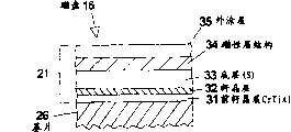
Referring to Fig. 2, wherein showed the thin layer in the specific embodiment of thin magnetic film dish 16.Substrate 26 is a glass.Be deposited on on-chip amorphous initial film and be called preceding inculating crystal layer 31.Inculating crystal layer 32 is deposited on the preceding inculating crystal layer.Preceding inculating crystal layer all is relative thin layer with inculating crystal layer usually.The material that proposition is used as inculating crystal layer comprises chromium, titanium, tantalum, Ni
3P, MgO, carbon, tungsten, AlN, FeAl, NiAl and RuAl.In the United States Patent (USP) 5789056 of authorizing people such as Bian, disclosed the use of CrTi inculating crystal layer.Normally chromium or evanohm bottom 33, for example Cr, CrV and CrTi after the inculating crystal layer.Ferromagnetic layer 34 in the film is based on the various alloys of cobalt, nickel and iron.For example, normally used alloy is CoPtCr.Add element for example tantalum and boron in being usually used in magnetic alloy.The protection external coating is used to improve wearing quality and corrosion stability.The embodiment of above-mentioned dish is one of many possibilities.Seediness crystal layer, many bottoms and many magnetospheres have for example been proposed in the prior art.
As mentioned above, the preferred orientation (PO) that forms the various crystalline materials of each layer on disk needn't be the exclusiveness orientation that can find in the material, but is the most significant orientation.When under the temperature that enough raises, on having applied the AlMg substrate of NiP, during sputtering deposit Cr bottom, form [200] PO usually.This PO promotes the epitaxial growth of [11-20] PO of hexagonal intensive (hcp) cobalt-base alloy, thereby has improved the magnetic property of disk.[11-20] PO is meant that its (11-20) crystal face mainly is parallel to the hexagonal structure film of film surface.Equally, [10-10] PO is meant that its (10-10) crystal face mainly is parallel to the film of the hexagonal structure of film surface.[10-10] PO can epitaxial growth on the suitable bottom of the PO with [112].
A kind of technology that is used to improve the magnetic recording property on thin film disk in the prior art is the circumference polishing, is used to produce trickle " cut " (the circumference texture) that is orientated along the magnetic track on the magnetic disk surface (concentric circles) usually.The texture yardstick of commercially available thin film disk is the microstructure with the peak-paddy that is generally less than 5nm.Concerning unbred naked eyes, the texture of 5nm shows as minute surface.In order to realize United States Patent (USP) 5490809 described so trickle circumference textures of people such as Jones for example, special polissoir must be arranged.On it deposit the surface topography of film can have remarkable influence to the mode of film nucleation and growth, and also act on its performance.For the magnetic alloy of wide region, the so-called circumference texture on the disk is commonly used to influence the plane magnetic anisotropy.For longitudinal recording, having specific diameter at circumferencial direction is useful to the higher coercive force of direction (Hc) sometimes.Circumference Hc is called orientation ratio (OR) with the ratio of Hc radially.For example, the United States Patent (USP) 4287225 of Kneller has been introduced him and is used the circumference texture of amorphous SmCo alloy can obtain uniaxial magnetic anisotropy (being OR>1).Other people adopt body centred cubic (bbc) alloy to obtain similar effects.Popular disk generally uses hexagonal intensive (hcp) cobalt-base alloy, and great majority (but not being whole) circumference texture disk has OR>1.
It is as follows that the United States Patent (USP) 6567236 of authorizing people such as Doerner has been introduced the preferred embodiment of layer structure: the preceding inculating crystal layer that preferably adopts CrTi, the preferred inculating crystal layer that adopts RuAl, preferably adopt the bottom of CrTi, preferably adopt the ferromagnetic bottom of CoCr, preferably adopt antiferromagnetic coupling/separation layer of Ru; The top ferromagnetic structure comprises: preferably adopt thin first sublayer of CoCr, CoCrB or CoPtCrB material, and thicker second sublayer of preferably adopting the CoPtCrB material, its magnetic moment is less than first sublayer.
Summary of the invention
The applicant discloses the thin film magnetic recording media structure with the preceding inculating crystal layer of CrTiAl.Inculating crystal layer presents amorphous or nanocrystalline structure before the CrTiAl.Inculating crystal layer has improved plane c axle orientation before the CrTiAl, has kept good orientation rate simultaneously.Pulse transition width (PW50) narrows down, and soft error rate is improved.Preferred inculating crystal layer is RuAl.
According to an aspect of the present invention, a kind of thin film disk that is used for magnetic recording comprises: have the preceding inculating crystal layer of CrTiAl of non crystalline structure, the inculating crystal layer of one deck at least before described on the inculating crystal layer; The bottom of one deck at least on described inculating crystal layer; And the magnetosphere of one deck at least on described bottom.
According to a further aspect in the invention, a kind of thin magnetic film storage medium comprises: substrate; Be deposited on on-chip CrTiAl layer, this CrTiAl layer has amorphous or nanocrystalline structure; RuAl layer on the CrTiAl layer, this RuAl layer has B2 crystalline texture; The bottom of one deck at least on the RuAl layer; The magnetosphere of one deck at least on bottom.
According to a further aspect in the invention, a kind of disc driver comprises: comprise the magnetic sensor that reads with write head; Main shaft; Be installed in the thin film disk on the main shaft, this thin film disk comprises RuAl layer with B2 crystalline texture on CrTiAl layer, the CrTiAl layer and the magnetosphere of one deck at least on the RuAl layer, and this CrTiAl layer has amorphous or nanocrystalline structure.
According to a further aspect in the invention, a kind of method of making the thin magnetic film storage medium may further comprise the steps: deposit CrTiAl layer on substrate, and this CrTiAl layer has amorphous or nanocrystalline structure; Deposit RuAl layer on the CrTiAl layer, wherein RuAl has B2 crystalline texture; Deposit multilayer on the RuAl layer, this multilayer comprise one deck magnetosphere at least.
Description of drawings
Fig. 1 is the synoptic diagram of prior art, has showed the magnetic head in the disc driver and the relation of associated components.
Fig. 2 is the layer structure of thin film disk, wherein can use preceding inculating crystal layer of the present invention.
Fig. 3 is the synoptic diagram that magnetosphere piles up, and comprises ferromagnetic layer on the bilayer that is used for thin film disk of the present invention.
Embodiment
For the vertical medium on glass or other non-magnetic substrate, importantly make the maximization of c axial plane crystalline orientation, and keep the orientation rate.Help good plane c axle orientation when inculating crystal layer material is used for substrate level and smooth or polishing arbitrarily before some, but result and unsatisfactory when being used for the substrate of circumference texture, because their orientation ratio (OR) is very low.Preceding inculating crystal layer described here is the amorphous or the nanometer crystal layer of CrTiAl alloy, is particularly suitable for being used in the substrate of circumference texture, because it helps to realize that good plane c axle is orientated, and high orientation ratio.The combination of these characteristics causes narrower transformation pulse width (PW50), and has improved soft error rate (SER).
Referring to Fig. 2 and 3, it has showed the thin layer of implementing in the thin film disk 16 of the present invention.In the embodiment shown in Fig. 2 and 3, CrTiAl layer 31 be direct sputtering deposit on substrate surface 26, substrate can be glass or any other suitable material or surface.Inculating crystal layer can use with various inculating crystal layers before the CrTiAl of the present invention.Inculating crystal layer also can be formed the CrTiAl/RuAl double-decker with preferred inculating crystal layer RuAl before the CrTiAl.The CrTiAl layer can make RuAl layer 32 subsequently keep very thin, so provide cost savings very high RuAl.When using CrTiAl, also can make chromium basalis 33 keep very thinly.
As everyone knows, by the bottom that deposit at first has (200) preferred orientation, also can make the growth of cobalt-base alloy thin magnetic film have (11-20) plane preferred orientation.RuAl inculating crystal layer with B2 crystalline texture is used for obtaining to have the bottom of (200) preferred orientation and having the cobalt-base alloy thin magnetic film that (11-20) preferred planar is orientated.(11-20) PO is for realizing that the orientation ratio greater than 1 is important.
Fig. 2 and 3 has showed the layer structure 21 of the preferred embodiment of the present invention in the thin film disk 16.This film comprises the magnetic layer-structure that has according to the antiferromagnetic coupling magnetosphere of people's such as Doerner United States Patent (USP) 6567236.Inculating crystal layer 31 is the first films on the substrate 26 before the CrTiAl.Substrate 26 can be the substrate of any prior art, preferred glass.Most of preferred structures of the applicant comprise inculating crystal layer 32 (B2 crystalline texture) and the CrTi of RuAl
20Bottom 33.
Magnetic stack 34 is made up of multilayer shown in Figure 3.Preferred magnetic stack 34 has at least four layers that difference is different.Magnetic bottom 44 is the ferromagnetic materials that use in the thin film disk of prior art.The example of material that is applicable to magnetic bottom 44 comprises CoCr, CoPtCr or CoPtCrB, and the applicant thinks the CoCr of the chromium that preferably contains 10-14at%.Must select the thickness of magnetic bottom 44 with respect to the thickness of above-mentioned magnetic top level structure 40, but preferable range is the 10-30 dust.Coupling/separation layer 43 is nonmagnetic substances, selects its thickness to make magnetic top level structure 40 and magnetic bottom 44 antiferromagnetism be coupled.Ruthenium is the preferred material of coupling/separation layer 43, comprises chromium (Cr), rhodium (Rh), iridium (Ir), copper (Cu) and alloy thereof but prior art shows suitable material.The thickness of exchange/separation layer 43 is according to prior art, and for example for rhodium coupling/separation layer 43, preferred target (target) thickness is the 6 Izod right sides.Magnetic top layer 40 preferably includes the double-decker of two kinds of different ferromagnetic materials.(first) sublayer 42 at interface is the film with material of higher moment, and magnetic moment is greater than second sublayer.The preferred material of the sublayer 42 at interface is CoCr, CoCrB and CoPtCrB.Preferred thickness approximately is the 3-15 dust.The sub-layer material at interface is chosen the material with magnetic moment higher than second sublayer.As can be known from prior art, pass through the content of the alloy element, for example platinum, chromium and the boron that are contained, can make the magnetic moment of cobalt-base alloy various reduction is arranged.Therefore, though first and second sublayers can comprise identical element, in order to realize the target of higher magnetic moment in first sublayer, atomic percent is different.
Second sublayer has lower magnetic moment, and thicker than first sublayer; Its composition and thickness are selected to when making up with first sublayer Mrt are provided, and this is essential to whole magnetic texure.The magnetic top level structure that comprises first and second sublayers is designed to have the Mrt bigger than magnetic bottom, so that the Net magnetic moment during zero externally-applied magnetic field is lower, but non-vanishing.
The preferred thickness of inculating crystal layer is that 10nm is to 30nm before the CrTiAl.Preferred compositing range is the aluminium of 5at% to 20at%, and all the other are atomic percent chromium and titaniums about equally.The RuAl layer is the crystalline texture that is deposited with B2, is the aluminium of 50at% substantially therefore.
With the on-chip Cr of circumference texture
50Ti
50Among the medium contrast experiment of preceding inculating crystal layer, find the Cr of preceding inculating crystal layer of the present invention
44Ti
44Al
12Embodiment has realized the reduction of the significance degree of full width at half maximum (FWHM) X-ray diffraction to (11-20) cobalt peak.The orientation ratio of being realized is identical for two kinds of films.This shows that for identical OR value inculating crystal layer has produced c axial plane orientation preferably before the CrTiAl.
For adopting Cr
50Ti
50And Cr
44Ti
44Al
12The disk that preceding inculating crystal layer is made, table 1 has provided transformation pulse width (PW50) and soft error rate (SER).Data show at Cr
44Ti
44Al
12In these two parameters of preceding inculating crystal layer, performance all is improved.
Table 1
| Preceding inculating crystal layer | PW50(nm) | log(SER) |
| Cr 50Ti 50 | 118.6 | -4.7 |
| Cr 44Ti 44Al 12 | 117.5 | -5.1 |
The above-mentioned atomic percent that provides is not consider to be present in inevitably small amount of impurities among the sputtered film, and this knows to those skilled in the art.Introduced the present invention at specific embodiment, but to those skilled in the art, other of preceding inculating crystal layer of the present invention uses and application is conspicuous.
Claims (13)
1. thin film disk that is used for magnetic recording comprises:
The preceding inculating crystal layer of CrTiAl with non crystalline structure,
The inculating crystal layer of one deck at least before described on the inculating crystal layer;
The bottom of one deck at least on described inculating crystal layer; And
The magnetosphere of one deck at least on described bottom.
2. according to the thin film disk of claim 1, wherein said inculating crystal layer is the RuAl with B2 crystalline texture.
3. according to the thin film disk of claim 1, wherein inculating crystal layer has 5 to 20at% aluminium before the CrTiAl, and all the other are roughly the same chromium of atomic percent and titanium.
4. according to the thin film disk of claim 1, wherein inculating crystal layer is deposited on the non-metal base of circumference texture before the CrTiAl.
5. thin magnetic film storage medium comprises:
Substrate;
Be deposited on on-chip CrTiAl layer, this CrTiAl layer has amorphous or nanocrystalline structure;
RuAl layer on the CrTiAl layer, this RuAl layer has B2 crystalline texture;
The bottom of one deck at least on the RuAl layer;
The magnetosphere of one deck at least on bottom.
6. according to the thin magnetic film storage medium of claim 5, wherein CrTiAl has 5 to 20at% aluminium, and all the other are roughly the same chromium of atomic percent and titanium.
7. according to the thin magnetic film storage medium of claim 5, wherein CrTiAl thick 10 to 30nm.
8. method of making the thin magnetic film storage medium may further comprise the steps:
Deposit CrTiAl layer on substrate, this CrTiAl layer has amorphous or nanocrystalline structure;
Deposit RuAl layer on the CrTiAl layer, wherein RuAl has B2 crystalline texture;
Deposit multilayer on the RuAl layer, this multilayer comprise one deck magnetosphere at least.
9. method according to Claim 8, wherein CrTiAl has 5 to 20at% aluminium, and all the other are roughly the same chromium of atomic percent and titanium.
10. method according to Claim 8, wherein CrTiAl thick 10 to 30nm.
11. a disc driver comprises:
Comprise the magnetic sensor that reads with write head;
Main shaft;
Be installed in the thin film disk on the main shaft, this thin film disk comprises RuAl layer with B2 crystalline texture on CrTiAl layer, the CrTiAl layer and the magnetosphere of one deck at least on the RuAl layer, and this CrTiAl layer has amorphous or nanocrystalline structure.
12. according to the disc driver of claim 11, wherein CrTiAl has 5 to 20at% aluminium, all the other are roughly the same chromium of atomic percent and titanium.
13. according to the disc driver of claim 11, wherein CrTiAl thick 10 to 30nm.
Applications Claiming Priority (2)
| Application Number | Priority Date | Filing Date | Title |
|---|---|---|---|
| US10/608,866 | 2003-06-26 | ||
| US10/608,866 US6872478B2 (en) | 2003-06-26 | 2003-06-26 | Magnetic thin film media with a pre-seed layer of CrTiAl |
Publications (2)
| Publication Number | Publication Date |
|---|---|
| CN1598932A CN1598932A (en) | 2005-03-23 |
| CN100405466C true CN100405466C (en) | 2008-07-23 |
Family
ID=33540698
Family Applications (1)
| Application Number | Title | Priority Date | Filing Date |
|---|---|---|---|
| CNB2004100600825A Expired - Fee Related CN100405466C (en) | 2003-06-26 | 2004-06-25 | Magnetic thin film media with a pre-seed layer of CRTIAL |
Country Status (4)
| Country | Link |
|---|---|
| US (1) | US6872478B2 (en) |
| JP (1) | JP2005018975A (en) |
| CN (1) | CN100405466C (en) |
| SG (1) | SG118272A1 (en) |
Families Citing this family (7)
| Publication number | Priority date | Publication date | Assignee | Title |
|---|---|---|---|---|
| US8465853B2 (en) * | 2004-03-24 | 2013-06-18 | Marvell World Trade Ltd. | Glassy metal disk |
| JP4222965B2 (en) * | 2004-04-15 | 2009-02-12 | ヒタチグローバルストレージテクノロジーズネザーランドビーブイ | Perpendicular magnetic recording medium, method for manufacturing the same, and magnetic recording apparatus |
| US7419730B2 (en) * | 2004-08-31 | 2008-09-02 | Hitachi Global Storage Technologies Netherlands B.V. | Magnetic recording disk with antiferromagnetically coupled master layer including copper |
| US7651794B2 (en) * | 2005-04-28 | 2010-01-26 | Hitachi Global Storage Technologies Netherlands B.V. | Adhesion layer for thin film magnetic recording medium |
| JP2008140528A (en) * | 2006-12-05 | 2008-06-19 | Hitachi Global Storage Technologies Netherlands Bv | Perpendicular magnetic recording medium |
| US8941950B2 (en) | 2012-05-23 | 2015-01-27 | WD Media, LLC | Underlayers for heat assisted magnetic recording (HAMR) media |
| US9177585B1 (en) | 2013-10-23 | 2015-11-03 | WD Media, LLC | Magnetic media capable of improving magnetic properties and thermal management for heat-assisted magnetic recording |
Citations (4)
| Publication number | Priority date | Publication date | Assignee | Title |
|---|---|---|---|---|
| JPH1041134A (en) * | 1996-07-26 | 1998-02-13 | Showa Denko Kk | Magnetic recording medium and its manufacturing method |
| US20010016272A1 (en) * | 2000-02-09 | 2001-08-23 | Xiaoping Bian | Onset layer for thin film disk with CoPtCrB alloy |
| US20010033949A1 (en) * | 1999-11-12 | 2001-10-25 | Fujitsu Limited | Magnetic recording medium and magnetic storage apparatus |
| US6562488B1 (en) * | 1999-04-14 | 2003-05-13 | Seagate Technology Llc | CoCrPtTaNbB alloy for magnetic recording medium |
Family Cites Families (8)
| Publication number | Priority date | Publication date | Assignee | Title |
|---|---|---|---|---|
| DE2909891A1 (en) | 1979-03-14 | 1980-09-25 | Basf Ag | MAGNETIC RECORDING CARRIER |
| US5486134A (en) | 1992-02-27 | 1996-01-23 | Oliver Design, Inc. | System and method for texturing magnetic data storage disks |
| US5789056A (en) | 1997-01-30 | 1998-08-04 | International Business Machines Corporation | Thin film magnetic disk with chromium-titanium seed layer |
| DE60031373T2 (en) * | 1999-09-01 | 2007-09-20 | Showa Denko K.K. | MAGNETIC RECORDING MEDIUM AND DEVICE FOR MAGNETIC RECORDING |
| JP2001143250A (en) * | 1999-11-12 | 2001-05-25 | Fujitsu Ltd | Magnetic memory medium and magnetic storage device |
| US6593009B2 (en) | 2001-03-02 | 2003-07-15 | Hitachi Global Storage Technologies Netherlands N.V. | Magnetic thin film media with a pre-seed layer of CrTi |
| US6572989B2 (en) | 2001-06-06 | 2003-06-03 | International Business Machines Corporation | Thin film magnetic recording disk with a chromium-nickel pre-seed layer |
| US6567236B1 (en) | 2001-11-09 | 2003-05-20 | International Business Machnes Corporation | Antiferromagnetically coupled thin films for magnetic recording |
-
2003
- 2003-06-26 US US10/608,866 patent/US6872478B2/en not_active Expired - Lifetime
-
2004
- 2004-06-23 JP JP2004184643A patent/JP2005018975A/en active Pending
- 2004-06-25 SG SG200403804A patent/SG118272A1/en unknown
- 2004-06-25 CN CNB2004100600825A patent/CN100405466C/en not_active Expired - Fee Related
Patent Citations (4)
| Publication number | Priority date | Publication date | Assignee | Title |
|---|---|---|---|---|
| JPH1041134A (en) * | 1996-07-26 | 1998-02-13 | Showa Denko Kk | Magnetic recording medium and its manufacturing method |
| US6562488B1 (en) * | 1999-04-14 | 2003-05-13 | Seagate Technology Llc | CoCrPtTaNbB alloy for magnetic recording medium |
| US20010033949A1 (en) * | 1999-11-12 | 2001-10-25 | Fujitsu Limited | Magnetic recording medium and magnetic storage apparatus |
| US20010016272A1 (en) * | 2000-02-09 | 2001-08-23 | Xiaoping Bian | Onset layer for thin film disk with CoPtCrB alloy |
Also Published As
| Publication number | Publication date |
|---|---|
| CN1598932A (en) | 2005-03-23 |
| US6872478B2 (en) | 2005-03-29 |
| SG118272A1 (en) | 2006-01-27 |
| US20040265637A1 (en) | 2004-12-30 |
| JP2005018975A (en) | 2005-01-20 |
Similar Documents
| Publication | Publication Date | Title |
|---|---|---|
| US6567236B1 (en) | Antiferromagnetically coupled thin films for magnetic recording | |
| US6156404A (en) | Method of making high performance, low noise isotropic magnetic media including a chromium underlayer | |
| US7618722B2 (en) | Perpendicular magnetic recording media and magnetic storage apparatus using the same | |
| CN1260899A (en) | Manganese containing layer for magnetic recording media | |
| KR100469531B1 (en) | Magnetic recording disk | |
| US20130045396A1 (en) | Ferromagnetically coupled magnetic recording media | |
| EP1801790A1 (en) | Perpendicular magnetic recording disk with ultrathin nucleation film and method for making the disk | |
| US5772857A (en) | Method of manufacturing CoCrTa/CoCrTaPt bi-layer magnetic thin films | |
| JP2003168207A (en) | Perpendicular magnetic recording medium and manufacturing method for perpendicular magnetic recording medium | |
| EP1655724A2 (en) | Magnetic recording medium and magnetic storage apparatus | |
| US7976964B2 (en) | Disk drive with laminated magnetic thin films with sublayers for magnetic recording | |
| CN100405466C (en) | Magnetic thin film media with a pre-seed layer of CRTIAL | |
| US6593009B2 (en) | Magnetic thin film media with a pre-seed layer of CrTi | |
| US6852430B2 (en) | Magnetic thin film media with a pre-seed layer of CrTi | |
| CN1322494C (en) | Thin film media with a dual seed layer of rual/nialb | |
| US20060210834A1 (en) | Laminated magnetic thin films with sublayers for magnetic recording | |
| US6475611B1 (en) | Si-containing seedlayer design for multilayer media | |
| CN1288637C (en) | Magnetic thin film media with a bi-layer structure of CrTi/NiP | |
| JP2004227717A (en) | Magnetic recording medium and its manufacturing method | |
| US20040258959A1 (en) | Magnetic recording medium and method of forming thereof, and underlayer structure thereof | |
| US6908689B1 (en) | Ruthenium-aluminum underlayer for magnetic recording media | |
| US6849326B1 (en) | Niobium alloy seedlayer for magnetic recording media | |
| US6821654B1 (en) | CrMoTa underlayer | |
| US7407719B1 (en) | Longitudinal magnetic media having a granular magnetic layer | |
| JP2003085725A (en) | Perpendicular magnetic recording medium and method of manufacturing the same |
Legal Events
| Date | Code | Title | Description |
|---|---|---|---|
| C06 | Publication | ||
| PB01 | Publication | ||
| C10 | Entry into substantive examination | ||
| SE01 | Entry into force of request for substantive examination | ||
| C14 | Grant of patent or utility model | ||
| GR01 | Patent grant | ||
| C17 | Cessation of patent right | ||
| CF01 | Termination of patent right due to non-payment of annual fee |
Granted publication date: 20080723 Termination date: 20110625 |