Summary of the invention
In the semiconductor device technical field, exist the demand that HMOS high-speed metal oxide semiconductor field-effect transistor (MOSFET) is provided.Existing in this technical field provides formed high speed complementation metal-oxide semiconductor (CMOS) need for equipment in known transistor material.Existing in this technical field provides the need for equipment of the high speed complementation metal-oxide semiconductor (CMOS) with reduced series resistance source/drain.
These and other demand can be reached by embodiments of the invention, the invention provides a kind of semiconductor device, comprise: be formed with transistorized semiconductor substrate on it, this transistor comprises N channel metal oxide semiconductor transistor and P-channel metal-oxide-semiconductor transistor; Comprising transistorized this transistor of this N channel metal oxide semiconductor transistor and this P-channel metal-oxide-semiconductor includes and is formed at the grid that has opposing sidewalls on this base material; Be formed at the active region in this base material; Be formed on insulative sidewall spacers other along this grid opposing sidewalls and that contact with this grid opposing sidewalls; And being embedded in conductive layer in this sidewall spacer, this conductive layer and this grid and this active region are electrically insulated; This N channel metal oxide semiconductor transistor and the transistorized active region of this P-channel metal-oxide-semiconductor have the series resistance of stand-alone programization.
Semiconductor device of the present invention includes and forms transistorized semiconductor substrate thereon.This transistor comprises and has opposing sidewalls and be formed at grid on this base material.In this base material, be formed with active region.Insulative sidewall spacers is formed at along this grid opposing sidewalls side and is contacted with this grid opposing sidewalls.In this sidewall spacer, be embedded with conductive layer.This embedded conductive layer system is electrically insulated from this grid and this active region.
Previous described demand also can be reached by the method part embodiment of formation semiconductor device provided by the present invention, this forms the method for semiconductor device, comprise: provide to be formed with transistorized semiconductor substrate on it, this transistor comprises N channel metal oxide semiconductor transistor and P-channel metal-oxide-semiconductor transistor simultaneously; Comprise transistorized this transistor of this N channel metal oxide semiconductor transistor and this P-channel metal-oxide-semiconductor and include and be formed at the grid that has opposing sidewalls on this base material, and be formed at the active region in this base material; On this grid and active region, form first insulating barrier; Depositing conducting layer on this first insulating barrier; Selective removal partially conductive layer is to expose part first insulating barrier that is covered in this grid and this active region; Deposition second insulating barrier on this conductive layer and first insulating barrier; And remove part first insulating barrier and second insulating barrier to form sidewall spacer other along this grid opposing sidewalls and that contact with this grid opposing sidewalls, be embedded with this conductive layer in this sidewall spacer; The series resistance of this N channel metal oxide semiconductor transistor and the transistorized active region of this P-channel metal-oxide-semiconductor is by stand-alone programization.
The method of this invention can comprise providing and is formed with transistorized semiconductor substrate on it.This transistor includes and is formed at the grid that has opposing sidewalls on this semiconductor substrate, and is formed at the active region in this base material.On this grid and active region, be formed with first insulating barrier, and on this first insulating barrier, deposit conductive layer.Selective removal partially conductive layer is to expose outside this first insulating barrier part that is covered in this grid and this active region.On this conductive layer and first insulating barrier, form second insulating barrier.Remove part first insulating barrier and second insulating barrier to form sidewall spacer other along this grid opposing sidewalls and that contact with this grid opposing sidewalls, be embedded with this conductive layer in this sidewall spacer.
The present invention can reach the demand of improving high speed transistor, for example complementary metal oxide semiconductor (CMOS) device.The present invention can reach the demand that has electrically programmed transistor, reduces series resistance source/drain regions.
When consult accompanying drawing be below the present invention describe in detail after, the present invention aforementioned and other feature, viewpoint and advantage will become obvious.
Embodiment
The present invention can produce improvement high-speed semiconductor device.The present invention can produce has the metal-oxide semiconductor transistor that reduces source/drain region series resistance.Those benefits are to provide by being embedded into the conductive layer part in the transistorized gate sidewall spacer of metal-oxide semiconductor that is electrically insulated.
This is embedded into, and insulation conductive layer in transistorized gate sidewall spacer can be unsteady (floating) or biasing (biased) adheres to bias (biaspotential) by contact point (contact).This embedded conductive layer in order to stored charge in the position the highly doped source/drain extension below this embedded conductive layer.This embedded conductive layer allow this source/drain region series resistance by this transistor gate (when this embedded conductive layer when floating) or by in addition sequencing of bias (when this embedded conductive layer during) for biasing.
The present invention is with the formation of accompanying drawings semiconductor device and described.Yet it is an illustration of the presently claimed invention only, is not in order to be limited to manufacturing illustrated in this accompanying drawing and specific device.
As shown in Figure 1, provide for example semiconductor substrate 10 of silicon wafer, this semiconductor substrate 10 includes basalis 12, wherein is formed with active region 14.On this active region 14, be formed with gate insulator 16.This gate insulator 16 typical cases are the oxide layer of thick about 10 dust to 100 dusts, and thermal oxidation that it can be by this semiconductor substrate or the deposition technique by for example chemical vapor deposition (CVD) form.This semiconductor substrate 10 also includes grid 18, and this grid 18 has the opposing sidewalls 20 that is formed on this gate insulator 16.This grid 18 typical cases include the polysilicon layer of thick about 100 dust to 5000 dusts.In part embodiment of the present invention, this grid 18 has about 100 dust to 1000 dusts of thickness.
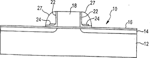
As shown in Figure 2, on this grid 18, be formed with first insulating barrier 22.In part embodiment, this first insulating barrier 22 is the silicon nitrogen layer of thick about 50 dust to 300 dusts.In addition, this first insulating barrier 22 can be by this grid 18 of thermal oxidation and this active region 14 formed oxide layers, or other insulating barrier that is fit to.
As shown in Figure 3, on this first insulating barrier 22, be formed with the conductive layer 24 of thick about 50 dust to 300 dusts.This conductive layer 24 for example is polysilicon, metal or metal silicide.The polysilicon layer typical case deposits by chemical vapour deposition technique.For example the metal level of aluminium, titanium, tungsten, nickel and cobalt is that the metal deposition technique of commonly using by for example chemical vapour deposition (CVD) or sputter deposits.In addition, in part embodiment of the present invention, this conductive layer is a metal silicide, and it is that the metal level 44 of titanium, tungsten, nickel or cobalt forms by for example depositing behind the deposit spathic silicon layer 42 as shown in Figure 8 again.As shown in Figure 9, the generation of this metal silicide is by heating this semiconductor substrate 10 to the temperature of this polysilicon layer of enough reactions 42 with this metal level 44, and forms metal silicified layer 46.
As shown in Figure 4, this conductive layer 24 manifests first insulating barrier that is covered in this grid 18 and partly is covered in this active region 14 through the selectivity patternization to remove partially conductive layer 24, and keeps the partially conductive layer 24 of contiguous this relative gate lateral wall 20.The reserve part width of this conductive layer 24 is about 100 dust to 1800 dusts.This conductive layer 24 is a patterning by known shielding and etching technique and in addition, for example by isotropic etching, anisotropic etching or in conjunction with isotropic etching and anisotropic etching.The selection of the application of this etching technique and special etch agent can be fit in order to remove the conductive of part specific pattern by selecting in known technology and the etchant.
In part embodiment of the present invention, this conductive layer 24 is by shielding and anisotropic etching and the selectivity patternization, then by shielding for the second time and follow-up isotropic etching to form this patterned conductive layer 24.This follow-up isotropic etching is in order to remove the partially conductive layer 24 that may still do extension behind anisotropic etching along these first insulating barrier, 22 sidewall sections 23, so that patterned conductive layer 24 as shown in Figure 4 to be provided.In part embodiment of the present invention, also can not implement this and shield for the second time and follow-up isotropic etching.
As shown in Figure 5, behind this conductive layer 24 of selective removal, on this remaining conductive layer 24 and this first insulating barrier 22, deposit second insulating barrier 26.This second insulating barrier is typically the chemical vapor deposited silicon nitrogen layer of thick about 300 dust to 2000 dusts.This second insulating barrier 26 then utilizes the anisotropic etch techniques of known for example plasma etching and carries out anisotropic etching, to form the sidewall spacer that is embedded with conductive layer 24 27 as shown in Figure 6.In part embodiment of the present invention, use oxidation gate insulator 16 etch stop layer, to form this sidewall spacer 27 as etching silicon nitrogen insulating barrier 22,26.
In deep source/drain ion injection period, this sidewall spacer 27 covers this highly doped source/drain extension 30.This deep source/drain ion injects can be at this gate insulator 16 of etching to implement before or after exposing this active region 14.This gate insulator 16 is by anisotropy or isotropic etching and etching in addition.In part embodiment of the present invention, the gate insulator 16 of silicon oxide-containing for example is to use again the silica of resilient coating oxide etching (buffered oxide etch) or hydrofluoric acid to select etchant to carry out etching.
As shown in Figure 7, the active region 14 by formed this metal-oxide semiconductor transistor 32 of the present invention comprises regions and source 28 and highly doped source/drain extension 30.This embedded conductive layer 24 is arranged on this source/drain extension 30 and with this grid 18 and active region 14 and is electrically insulated.
This embedded conductive layer 24 can be electrically unsteady (electrically floating) as shown in Figure 7, or biasing as shown in figure 10 (biased).This conductive layer 24 can be by being setovered the contact of this embedded conductive layer to the voltage source of for example potentiometer (potentiostat).These transistor 32 side-looking parts as shown in figure 10, bias voltage (bias) provides to this embedded conductive layer 24 by the lead 34 from voltage source 36.In part embodiment of the present invention, transistorized this embedded conductive layer 24 of N channel metal semiconductor (NMOS) will bias to negative potential, and transistorized this embedded conductive layer of P channel metal semiconductor (PMOS) will bias to positive potential.
Can provide complementary metal oxide semiconductor (CMOS) device according to the present invention by on same substrate, forming N channel metal semiconductor and P channel metal semiconductor.Except different bias voltages on this N channel metal semiconductor and P channel metal semiconductor embedded conductive layer 24, complementary metal oxide semiconductor device according to the present invention also comprises N channel metal semiconductor and the P mos transistors with unsteady embedded conductive layer 24.
Transistor of the present invention provides the series resistance ability of the transistorized regions and source of sequencing metal-oxide semiconductor, so that speeder to be provided.Be the bias voltage by being adjusted at this embedded conductive layer 24 in part embodiment of the present invention or select, and in addition the electrical resistance of the regions and source 28 of this transistor 32 by the material pattern that is used in this embedded conductive layer 24 " sequencing " to the electrical series impedance of demand.The factor that influences the electrical series impedance of source/drain of selection demand comprises the complementary metal oxide semiconductor device of channel dimensions, concentration of dopant, transistor requirements speed and balance.The complementary metal oxide semiconductor device generally is because the electron mobility in the N mos transistors usually can't balance greater than hole mobility in this P mos transistors.Utilize embedded conductive layer 24 can allow the series resistance stand-alone programization of the active region 14 of N channel metal semiconductor and P mos transistors, to reach the complementary metal oxide semiconductor of balance more.
In others, the semiconductor device with square-shaped sidewall spacers is formed on the semiconductor substrate.This semiconductor device 50 includes for example semiconductor substrate 52 of silicon wafer, provides gate insulator 53 to be formed on this semiconductor substrate.As shown in figure 11, polysilicon layer 54 is formed on this gate insulator 53, and the first silicon nitrogen layer 56 is formed on this polysilicon layer 54.Silicon oxide layer 58 is formed on this first silicon nitrogen layer 56, and (bottom anti-reflection coating, the second silicon nitrogen layer 60 BARC) is formed on this silicon oxide layer 58 to act as the bottom anti-reflective coating.
Have gate insulator 53, polysilicon layer 54, the first silicon nitrogen layer 56, silicon oxide layer 58, and the second silicon nitrogen layer 60 to form semiconductor device 50 on it patterned and form the stack architecture 61 with opposing sidewalls 63.This semiconductor device 50 then carries out ion and injects to be formed with highly doped source/drain extension 62.After forming this source/drain extension 62, this stack architecture 61 and semiconductor substrate are coated with insulating material, and this insulating layer material is formed with through anisotropic etching along the sidewall spacer 64 on this stack architecture opposing sidewalls 63 sides, as shown in figure 12.
As shown in figure 13, remove this second silicon nitrogen layer 60 in this stack architecture 61 certainly.This semiconductor device 50 reduces the height of this stack architecture 61 and sidewall spacer 64 through cmp (CMP), to form square-shaped sidewall spacers 64 as shown in figure 14.This first silicon nitrogen layer 56 act as the grinding stop layer during cmp.This semiconductor device 50 carries out deep ion subsequently and injects, to form the regions and source 66 of semiconductor device 50 as shown in figure 15.
In the embodiment explanation that this disclosed only is as the illustration purpose.It is not with being the scope of interpretation claims.For arbitrary those skilled in the art, comprise the embodiment wide variation but not in this certain illustrated in this part of exposing.