CN100390988C - Interconnection device and method - Google Patents
Interconnection device and method Download PDFInfo
- Publication number
- CN100390988C CN100390988C CNB008186499A CN00818649A CN100390988C CN 100390988 C CN100390988 C CN 100390988C CN B008186499 A CNB008186499 A CN B008186499A CN 00818649 A CN00818649 A CN 00818649A CN 100390988 C CN100390988 C CN 100390988C
- Authority
- CN
- China
- Prior art keywords
- electronic circuit
- circuit package
- interconnection
- package part
- pad
- Prior art date
- Legal status (The legal status is an assumption and is not a legal conclusion. Google has not performed a legal analysis and makes no representation as to the accuracy of the status listed.)
- Expired - Fee Related
Links
Images


Classifications
-
- H—ELECTRICITY
- H01—ELECTRIC ELEMENTS
- H01L—SEMICONDUCTOR DEVICES NOT COVERED BY CLASS H10
- H01L23/00—Details of semiconductor or other solid state devices
- H01L23/58—Structural electrical arrangements for semiconductor devices not otherwise provided for, e.g. in combination with batteries
- H01L23/64—Impedance arrangements
- H01L23/66—High-frequency adaptations
-
- H—ELECTRICITY
- H01—ELECTRIC ELEMENTS
- H01L—SEMICONDUCTOR DEVICES NOT COVERED BY CLASS H10
- H01L2224/00—Indexing scheme for arrangements for connecting or disconnecting semiconductor or solid-state bodies and methods related thereto as covered by H01L24/00
- H01L2224/01—Means for bonding being attached to, or being formed on, the surface to be connected, e.g. chip-to-package, die-attach, "first-level" interconnects; Manufacturing methods related thereto
- H01L2224/02—Bonding areas; Manufacturing methods related thereto
- H01L2224/04—Structure, shape, material or disposition of the bonding areas prior to the connecting process
- H01L2224/05—Structure, shape, material or disposition of the bonding areas prior to the connecting process of an individual bonding area
- H01L2224/0554—External layer
- H01L2224/05599—Material
-
- H—ELECTRICITY
- H01—ELECTRIC ELEMENTS
- H01L—SEMICONDUCTOR DEVICES NOT COVERED BY CLASS H10
- H01L2224/00—Indexing scheme for arrangements for connecting or disconnecting semiconductor or solid-state bodies and methods related thereto as covered by H01L24/00
- H01L2224/01—Means for bonding being attached to, or being formed on, the surface to be connected, e.g. chip-to-package, die-attach, "first-level" interconnects; Manufacturing methods related thereto
- H01L2224/26—Layer connectors, e.g. plate connectors, solder or adhesive layers; Manufacturing methods related thereto
- H01L2224/31—Structure, shape, material or disposition of the layer connectors after the connecting process
- H01L2224/32—Structure, shape, material or disposition of the layer connectors after the connecting process of an individual layer connector
- H01L2224/321—Disposition
- H01L2224/32151—Disposition the layer connector connecting between a semiconductor or solid-state body and an item not being a semiconductor or solid-state body, e.g. chip-to-substrate, chip-to-passive
- H01L2224/32221—Disposition the layer connector connecting between a semiconductor or solid-state body and an item not being a semiconductor or solid-state body, e.g. chip-to-substrate, chip-to-passive the body and the item being stacked
- H01L2224/32225—Disposition the layer connector connecting between a semiconductor or solid-state body and an item not being a semiconductor or solid-state body, e.g. chip-to-substrate, chip-to-passive the body and the item being stacked the item being non-metallic, e.g. insulating substrate with or without metallisation
-
- H—ELECTRICITY
- H01—ELECTRIC ELEMENTS
- H01L—SEMICONDUCTOR DEVICES NOT COVERED BY CLASS H10
- H01L2224/00—Indexing scheme for arrangements for connecting or disconnecting semiconductor or solid-state bodies and methods related thereto as covered by H01L24/00
- H01L2224/01—Means for bonding being attached to, or being formed on, the surface to be connected, e.g. chip-to-package, die-attach, "first-level" interconnects; Manufacturing methods related thereto
- H01L2224/42—Wire connectors; Manufacturing methods related thereto
- H01L2224/44—Structure, shape, material or disposition of the wire connectors prior to the connecting process
- H01L2224/45—Structure, shape, material or disposition of the wire connectors prior to the connecting process of an individual wire connector
- H01L2224/45001—Core members of the connector
- H01L2224/4501—Shape
- H01L2224/45012—Cross-sectional shape
- H01L2224/45014—Ribbon connectors, e.g. rectangular cross-section
-
- H—ELECTRICITY
- H01—ELECTRIC ELEMENTS
- H01L—SEMICONDUCTOR DEVICES NOT COVERED BY CLASS H10
- H01L2224/00—Indexing scheme for arrangements for connecting or disconnecting semiconductor or solid-state bodies and methods related thereto as covered by H01L24/00
- H01L2224/01—Means for bonding being attached to, or being formed on, the surface to be connected, e.g. chip-to-package, die-attach, "first-level" interconnects; Manufacturing methods related thereto
- H01L2224/42—Wire connectors; Manufacturing methods related thereto
- H01L2224/47—Structure, shape, material or disposition of the wire connectors after the connecting process
- H01L2224/48—Structure, shape, material or disposition of the wire connectors after the connecting process of an individual wire connector
- H01L2224/4805—Shape
- H01L2224/4809—Loop shape
- H01L2224/48091—Arched
-
- H—ELECTRICITY
- H01—ELECTRIC ELEMENTS
- H01L—SEMICONDUCTOR DEVICES NOT COVERED BY CLASS H10
- H01L2224/00—Indexing scheme for arrangements for connecting or disconnecting semiconductor or solid-state bodies and methods related thereto as covered by H01L24/00
- H01L2224/01—Means for bonding being attached to, or being formed on, the surface to be connected, e.g. chip-to-package, die-attach, "first-level" interconnects; Manufacturing methods related thereto
- H01L2224/42—Wire connectors; Manufacturing methods related thereto
- H01L2224/47—Structure, shape, material or disposition of the wire connectors after the connecting process
- H01L2224/48—Structure, shape, material or disposition of the wire connectors after the connecting process of an individual wire connector
- H01L2224/481—Disposition
- H01L2224/48151—Connecting between a semiconductor or solid-state body and an item not being a semiconductor or solid-state body, e.g. chip-to-substrate, chip-to-passive
- H01L2224/48221—Connecting between a semiconductor or solid-state body and an item not being a semiconductor or solid-state body, e.g. chip-to-substrate, chip-to-passive the body and the item being stacked
- H01L2224/48225—Connecting between a semiconductor or solid-state body and an item not being a semiconductor or solid-state body, e.g. chip-to-substrate, chip-to-passive the body and the item being stacked the item being non-metallic, e.g. insulating substrate with or without metallisation
- H01L2224/48227—Connecting between a semiconductor or solid-state body and an item not being a semiconductor or solid-state body, e.g. chip-to-substrate, chip-to-passive the body and the item being stacked the item being non-metallic, e.g. insulating substrate with or without metallisation connecting the wire to a bond pad of the item
-
- H—ELECTRICITY
- H01—ELECTRIC ELEMENTS
- H01L—SEMICONDUCTOR DEVICES NOT COVERED BY CLASS H10
- H01L2224/00—Indexing scheme for arrangements for connecting or disconnecting semiconductor or solid-state bodies and methods related thereto as covered by H01L24/00
- H01L2224/01—Means for bonding being attached to, or being formed on, the surface to be connected, e.g. chip-to-package, die-attach, "first-level" interconnects; Manufacturing methods related thereto
- H01L2224/42—Wire connectors; Manufacturing methods related thereto
- H01L2224/47—Structure, shape, material or disposition of the wire connectors after the connecting process
- H01L2224/48—Structure, shape, material or disposition of the wire connectors after the connecting process of an individual wire connector
- H01L2224/484—Connecting portions
- H01L2224/48463—Connecting portions the connecting portion on the bonding area of the semiconductor or solid-state body being a ball bond
- H01L2224/48465—Connecting portions the connecting portion on the bonding area of the semiconductor or solid-state body being a ball bond the other connecting portion not on the bonding area being a wedge bond, i.e. ball-to-wedge, regular stitch
-
- H—ELECTRICITY
- H01—ELECTRIC ELEMENTS
- H01L—SEMICONDUCTOR DEVICES NOT COVERED BY CLASS H10
- H01L2224/00—Indexing scheme for arrangements for connecting or disconnecting semiconductor or solid-state bodies and methods related thereto as covered by H01L24/00
- H01L2224/01—Means for bonding being attached to, or being formed on, the surface to be connected, e.g. chip-to-package, die-attach, "first-level" interconnects; Manufacturing methods related thereto
- H01L2224/42—Wire connectors; Manufacturing methods related thereto
- H01L2224/47—Structure, shape, material or disposition of the wire connectors after the connecting process
- H01L2224/49—Structure, shape, material or disposition of the wire connectors after the connecting process of a plurality of wire connectors
- H01L2224/491—Disposition
- H01L2224/4912—Layout
- H01L2224/49175—Parallel arrangements
-
- H—ELECTRICITY
- H01—ELECTRIC ELEMENTS
- H01L—SEMICONDUCTOR DEVICES NOT COVERED BY CLASS H10
- H01L2224/00—Indexing scheme for arrangements for connecting or disconnecting semiconductor or solid-state bodies and methods related thereto as covered by H01L24/00
- H01L2224/73—Means for bonding being of different types provided for in two or more of groups H01L2224/10, H01L2224/18, H01L2224/26, H01L2224/34, H01L2224/42, H01L2224/50, H01L2224/63, H01L2224/71
- H01L2224/732—Location after the connecting process
- H01L2224/73251—Location after the connecting process on different surfaces
- H01L2224/73265—Layer and wire connectors
-
- H—ELECTRICITY
- H01—ELECTRIC ELEMENTS
- H01L—SEMICONDUCTOR DEVICES NOT COVERED BY CLASS H10
- H01L2224/00—Indexing scheme for arrangements for connecting or disconnecting semiconductor or solid-state bodies and methods related thereto as covered by H01L24/00
- H01L2224/80—Methods for connecting semiconductor or other solid state bodies using means for bonding being attached to, or being formed on, the surface to be connected
- H01L2224/85—Methods for connecting semiconductor or other solid state bodies using means for bonding being attached to, or being formed on, the surface to be connected using a wire connector
- H01L2224/8538—Bonding interfaces outside the semiconductor or solid-state body
- H01L2224/85399—Material
-
- H—ELECTRICITY
- H01—ELECTRIC ELEMENTS
- H01L—SEMICONDUCTOR DEVICES NOT COVERED BY CLASS H10
- H01L24/00—Arrangements for connecting or disconnecting semiconductor or solid-state bodies; Methods or apparatus related thereto
- H01L24/01—Means for bonding being attached to, or being formed on, the surface to be connected, e.g. chip-to-package, die-attach, "first-level" interconnects; Manufacturing methods related thereto
- H01L24/42—Wire connectors; Manufacturing methods related thereto
- H01L24/47—Structure, shape, material or disposition of the wire connectors after the connecting process
- H01L24/48—Structure, shape, material or disposition of the wire connectors after the connecting process of an individual wire connector
-
- H—ELECTRICITY
- H01—ELECTRIC ELEMENTS
- H01L—SEMICONDUCTOR DEVICES NOT COVERED BY CLASS H10
- H01L24/00—Arrangements for connecting or disconnecting semiconductor or solid-state bodies; Methods or apparatus related thereto
- H01L24/01—Means for bonding being attached to, or being formed on, the surface to be connected, e.g. chip-to-package, die-attach, "first-level" interconnects; Manufacturing methods related thereto
- H01L24/42—Wire connectors; Manufacturing methods related thereto
- H01L24/47—Structure, shape, material or disposition of the wire connectors after the connecting process
- H01L24/49—Structure, shape, material or disposition of the wire connectors after the connecting process of a plurality of wire connectors
-
- H—ELECTRICITY
- H01—ELECTRIC ELEMENTS
- H01L—SEMICONDUCTOR DEVICES NOT COVERED BY CLASS H10
- H01L2924/00—Indexing scheme for arrangements or methods for connecting or disconnecting semiconductor or solid-state bodies as covered by H01L24/00
- H01L2924/0001—Technical content checked by a classifier
- H01L2924/00014—Technical content checked by a classifier the subject-matter covered by the group, the symbol of which is combined with the symbol of this group, being disclosed without further technical details
-
- H—ELECTRICITY
- H01—ELECTRIC ELEMENTS
- H01L—SEMICONDUCTOR DEVICES NOT COVERED BY CLASS H10
- H01L2924/00—Indexing scheme for arrangements or methods for connecting or disconnecting semiconductor or solid-state bodies as covered by H01L24/00
- H01L2924/01—Chemical elements
- H01L2924/01027—Cobalt [Co]
-
- H—ELECTRICITY
- H01—ELECTRIC ELEMENTS
- H01L—SEMICONDUCTOR DEVICES NOT COVERED BY CLASS H10
- H01L2924/00—Indexing scheme for arrangements or methods for connecting or disconnecting semiconductor or solid-state bodies as covered by H01L24/00
- H01L2924/01—Chemical elements
- H01L2924/01029—Copper [Cu]
-
- H—ELECTRICITY
- H01—ELECTRIC ELEMENTS
- H01L—SEMICONDUCTOR DEVICES NOT COVERED BY CLASS H10
- H01L2924/00—Indexing scheme for arrangements or methods for connecting or disconnecting semiconductor or solid-state bodies as covered by H01L24/00
- H01L2924/01—Chemical elements
- H01L2924/01033—Arsenic [As]
-
- H—ELECTRICITY
- H01—ELECTRIC ELEMENTS
- H01L—SEMICONDUCTOR DEVICES NOT COVERED BY CLASS H10
- H01L2924/00—Indexing scheme for arrangements or methods for connecting or disconnecting semiconductor or solid-state bodies as covered by H01L24/00
- H01L2924/01—Chemical elements
- H01L2924/01039—Yttrium [Y]
-
- H—ELECTRICITY
- H01—ELECTRIC ELEMENTS
- H01L—SEMICONDUCTOR DEVICES NOT COVERED BY CLASS H10
- H01L2924/00—Indexing scheme for arrangements or methods for connecting or disconnecting semiconductor or solid-state bodies as covered by H01L24/00
- H01L2924/01—Chemical elements
- H01L2924/01082—Lead [Pb]
-
- H—ELECTRICITY
- H01—ELECTRIC ELEMENTS
- H01L—SEMICONDUCTOR DEVICES NOT COVERED BY CLASS H10
- H01L2924/00—Indexing scheme for arrangements or methods for connecting or disconnecting semiconductor or solid-state bodies as covered by H01L24/00
- H01L2924/013—Alloys
- H01L2924/014—Solder alloys
-
- H—ELECTRICITY
- H01—ELECTRIC ELEMENTS
- H01L—SEMICONDUCTOR DEVICES NOT COVERED BY CLASS H10
- H01L2924/00—Indexing scheme for arrangements or methods for connecting or disconnecting semiconductor or solid-state bodies as covered by H01L24/00
- H01L2924/10—Details of semiconductor or other solid state devices to be connected
- H01L2924/11—Device type
- H01L2924/14—Integrated circuits
- H01L2924/141—Analog devices
- H01L2924/1423—Monolithic Microwave Integrated Circuit [MMIC]
-
- H—ELECTRICITY
- H01—ELECTRIC ELEMENTS
- H01L—SEMICONDUCTOR DEVICES NOT COVERED BY CLASS H10
- H01L2924/00—Indexing scheme for arrangements or methods for connecting or disconnecting semiconductor or solid-state bodies as covered by H01L24/00
- H01L2924/15—Details of package parts other than the semiconductor or other solid state devices to be connected
- H01L2924/151—Die mounting substrate
- H01L2924/153—Connection portion
- H01L2924/1531—Connection portion the connection portion being formed only on the surface of the substrate opposite to the die mounting surface
- H01L2924/15313—Connection portion the connection portion being formed only on the surface of the substrate opposite to the die mounting surface being a land array, e.g. LGA
-
- H—ELECTRICITY
- H01—ELECTRIC ELEMENTS
- H01L—SEMICONDUCTOR DEVICES NOT COVERED BY CLASS H10
- H01L2924/00—Indexing scheme for arrangements or methods for connecting or disconnecting semiconductor or solid-state bodies as covered by H01L24/00
- H01L2924/15—Details of package parts other than the semiconductor or other solid state devices to be connected
- H01L2924/151—Die mounting substrate
- H01L2924/156—Material
- H01L2924/15786—Material with a principal constituent of the material being a non metallic, non metalloid inorganic material
- H01L2924/15787—Ceramics, e.g. crystalline carbides, nitrides or oxides
-
- H—ELECTRICITY
- H01—ELECTRIC ELEMENTS
- H01L—SEMICONDUCTOR DEVICES NOT COVERED BY CLASS H10
- H01L2924/00—Indexing scheme for arrangements or methods for connecting or disconnecting semiconductor or solid-state bodies as covered by H01L24/00
- H01L2924/19—Details of hybrid assemblies other than the semiconductor or other solid state devices to be connected
- H01L2924/1901—Structure
- H01L2924/1904—Component type
- H01L2924/19041—Component type being a capacitor
-
- H—ELECTRICITY
- H01—ELECTRIC ELEMENTS
- H01L—SEMICONDUCTOR DEVICES NOT COVERED BY CLASS H10
- H01L2924/00—Indexing scheme for arrangements or methods for connecting or disconnecting semiconductor or solid-state bodies as covered by H01L24/00
- H01L2924/30—Technical effects
- H01L2924/301—Electrical effects
- H01L2924/30105—Capacitance
-
- H—ELECTRICITY
- H01—ELECTRIC ELEMENTS
- H01L—SEMICONDUCTOR DEVICES NOT COVERED BY CLASS H10
- H01L2924/00—Indexing scheme for arrangements or methods for connecting or disconnecting semiconductor or solid-state bodies as covered by H01L24/00
- H01L2924/30—Technical effects
- H01L2924/301—Electrical effects
- H01L2924/30107—Inductance
-
- H—ELECTRICITY
- H01—ELECTRIC ELEMENTS
- H01L—SEMICONDUCTOR DEVICES NOT COVERED BY CLASS H10
- H01L2924/00—Indexing scheme for arrangements or methods for connecting or disconnecting semiconductor or solid-state bodies as covered by H01L24/00
- H01L2924/30—Technical effects
- H01L2924/301—Electrical effects
- H01L2924/3011—Impedance
- H01L2924/30111—Impedance matching
Abstract
An RF microcircuit package and interconnection device is disclosed which minimizes impedance mismatch between circuit elements. Multiple signal via and close proximity ground vias as well as tuned wire bonds are disclosed.
Description
The application is according to the HEI of u s company, and the pct international patent application that Inc. submitted December 20 in 2000 (having specified the All Countries except that the U.S.) proposes.
Technical field
The application relates to " encapsulation " technology of assembling microelectronic circuit, more specifically, relates to the transmission and method, the technology and equipment of Coupled RF signal between discrete component in encapsulation and the substrate.
Technical background
The microcircuit electronic product generally is assembled into single component an encapsulation and is assembled into.In fact, single component is selected comes out and is placed on the substrate.Substrate can be pliable and tough condensate rete, also can be hard potsherd.Substrate can have the multilayer circuit track, has interconnection line by path in the Z direction between each layer.Some assembly can be connected to pad on the substrate with direct electron such as scolder or adhesives.The pad of other assembly is not on the plane of substrate surface.In order to hold " highly " of these pads, having used lead-in wire to connect this method and having transmitted signal between the pad of Different Plane.
For example, common way always is that integrated circuit is bonding or be welded on the ceramic substrate, uses the method for " wire-bonded " to make the circuit interconnection circuit then between pad on the integrated circuit (IC) and the pad on the substrate." wire-bonded " is a little circuit loop, and electric current flows out from the pad on the IC, flows through the edge of IC, gets back to the surface of substrate then.In the course of processing, fusion is on IC rapidly for wire-bonded, and common quantum of output is 5 wire-bonded of per second.Path and wire-bonded form the acceptable signal path of encapsulation jointly, as long as relevant signal is " low frequency " signal.
But wire-bonded can decay and radiation signal in low GHz scope.Lead itself has a stray inductance, therefore becomes an important circuit element in the GHz scope.The traditional solution that reduces decay comprises that " wedge shape " engages and " band engages ".These two technology put forth effort to reduce the length of lead, thereby reduce the impedance of " lead ".
In the wedged-shaped technique method, lead forms the acute angle connection so that the total length minimum that connects in the pad outside.Can per second 2-3 speed that engages process this connection.Band engages with flat band lead and has substituted circular cross-section traditional in the wire-bonded.Band has a parasitic capacitance, and comparatively speaking, this is worth greater than inductance, can reduce decay.But successful band wire-bonded seriously relies on the laying of assembly.This processing procedure is extremely slow.
Originally also there is similar signal routes problem on one's body at substrate.On a multilager base plate, the linear signal track is arranged near ground plane usually.Therefore,, use known " strip line " technology, signal path can be designed to have constant rated impedance for the RF signal.But if signal path departs from the strip line path, and along the transmission of Z direction, then this asymmetry will produce not matching of impedance owing to relevant decay and reflection.Ceramic substrate is frangible, in order to guarantee mechanical strength, need increase thickness in the Z direction, thereby be easy to generate the unmatched problem of impedance especially.
Therefore, need improved interconnection device and method, to process high performance high-frequency circuit " encapsulation ".
Summary of the invention
Compared with prior art, the present invention proposes the method that solves impedance mismatch problem on the substrate.According to principle of the present invention, near the substrate joint fastener, formed an electric capacity.This electric capacity and wire-bonded " lead " have formed a resonant circuit.The function class of this circuit layout seemingly has the transmission line of rated characteristic impedance, has reduced the decay and the inhibition of reflected energy and emittance during coupled signal.
In a second aspect of the present invention, provide two or more paths to transmit the RF signal in the Z direction.During work, the coupling impedance of paralleled path forms the transmission line of signal.In another form, on the signal path side grounded circuit is set, to form the connection of similar transmission line.These different principles can be used singly or in combination to make high performance encapsulation.
Use the following advantage of being packaged with of these technical construction.The low-loss connection allows to repartition the RF Signal Processing Element to realize low cost or high-performance.For example, the interconnection line technology that lacks " ideal " can force people to use integrated circuit component, in this case, if utilize the present invention, just can use discrete circuit element, and not use integrated circuit component.This method of attachment also allows to carry out assembly and lays, thereby cuts down finished cost.These technology also allow to use conventional cheaply process equipment to process high performance RF encapsulation, and this point also means the reduction of cost.
Description of drawings
In conjunction with following accompanying drawing, in several illustrative embodiment, be described with function to various aspects of the present invention, wherein:
Fig. 1 is to use the sectional view of the encapsulation of various aspects of the present invention;
Fig. 2 is to use the plane graph of the encapsulation of some aspect of the present invention;
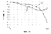
Fig. 3 shows the result that the return loss test is carried out in encapsulation to prototype;
Fig. 4 shows the result that the insertion loss test is carried out in encapsulation to prototype;
Fig. 5 has shown the performance of using the encapsulation that divides laminar substrate.
DETAILED DESCRIPTION OF THE PREFERRED
The disclosed content of the application in order to set forth disclosed content, is carried out brief explanation to method of testing based on performance test.Generally speaking, the device of testing has a RF input port and a RF output port.The radio-frequency power that enters circuit is done as a whole, and power output and input power are compared to measure " insertion loss "." insertion loss " is low good corresponding to performance.Owing to the do not match reflected energy that causes of impedance also can make performance reduce.This parameter is measured with return loss.The measurement result of return loss is generally negative, and therefore, return loss is high more, and performance is good more.
The measurement result of return loss and insertion loss is the function of frequency, all is that respective frequencies is drawn usually.For the new digital telephone technology that the broadband is provided, especially need the performance on the broadband.
Figure 1 shows that the cross section of encapsulation 30.The Z axle of arrow 9 these figure of expression.This encapsulation comprises substrate 16, can be ceramic, also can be polymeric films, and generally all is divided into which floor circuit.For clarity sake, the substrate shown in the figure 16 is for having only the structure of one deck.For the common situation of microwave, the lower surface of substrate is the ground plane 18 that is formed by the copper layer on the substrate 16.On this substrate 16, form a bars track by track 20 and ground plane 18 formed transmission lines.In the prior art, for any given baseplate material and dielectric constant, can calculate the accurate width of track 20 easily.Pass below the track 28 of track 20 from substrate 24 lower surfaces and engage with track 28.In an ordinary construction, ceramic substrate 24 can have several integrated circuits, also can have the discrete component that other divide laminar substrate 16 to be connected with pottery or polymeric films, thereby make a product.
In structure shown in Figure 1, substrate 24 by have many paths with ground plane guide to integrated circuit 22 below.First signal path 14 and alternate path 15 (see figure 2)s have formed the signal path of a Z direction together, are used for signal is passed to bonding region 12 on substrate 24 upper surfaces from transmission line 20.Compare with the prior art structure, the RF signal is divided into path 14 and the path 15 among Fig. 1 and Fig. 2.The position of first signal path 14 and secondary signal path is near grounded circuit 17.This two signal paths and subsidiary grounded circuit form constant impedance and connect together on the Z direction between transmission line 20 and the bonding welding pad 12.Obviously can obtain impedance matching property with more than one other grounded circuits or signal path.
In Fig. 1, the joint of lead 10 forms bonding welding pad 12 and connects to the electrical signal path that port 2 connects, intactly to describe test package 30.
Figure 2 shows that the plane graph of Fig. 1 layout.The X-Y axle of arrow 11 these structures of expression.Signal is from port one, and the transmission line that forms through track 20 and ground plane 18 (not shown) is connected and enters test package 30.This transmission line 20 is connected with track 28.Connecting track 28 illustrates with cut-away section in the drawings.This connects track 28 and is connected with secondary signal path 15 with first signal path 14.Each path represents that with a circle distance table between path 14 and the path 15 is shown spacing 32.The size of this spacing can be used to the transmission line character of " adjusting " signal path 14 and 15.
In Fig. 2, at the upper surface of substrate 24, the width of bonding welding pad 12 is represented with the exaggerative width that is labeled as 36.The bonding welding pad of this expansion has electric capacity with respect to the ground plane of substrate 22 and substrate 24.Just the electric capacity of pad at the inductance of " adjusting " lead 10 to produce the characteristics design impedance.Although among the figure this pad is expressed as and launches to have formed a T shape in the Y direction and connect, should be appreciated that also to form other shapes, and under some particular case, may more need other shapes.Many RF integrated circuits all have such characteristics, and promptly the density of interconnection line is low, thereby the outside of path can be used as this structure.Should also be noted that the T shape utilized the substrate of most of integrated circuits or the lower end advantage near ground plane.Corresponding circuit is the electric capacity between an inductance leads and earth terminal, has formed a band pass filter in signal path.
Spacing 32 between signal path 15 and the signal path 14 should be appreciated that, the accurate spacing of setting up needed characteristic impedance depends on the dielectric constant of substrate 24 and 16 and the propinquity of other ground connection features.Therefore, when providing the special package design, may need a plurality of signal paths.The shape and the position of first signal path 14 and secondary signal path 15 are illustrative, do not play the qualification effect.Similarly, signal path 14 and 15 grounded circuit 17 as a supplement, its position can be used to " adjusting " and connects.Since contiguous and contiguous with other stray capacitances with other ground structures, there is not accurate corresponding relation.
In various tests, the RF signal enters from port one, flows out from port 2.Depend on the quality of various connections between port one and the port 2 in the available horsepower of port 2, and test process records " return loss " and " insertion loss " between two ports.In general, in the composite test encapsulation, two kinds of layouts shown in Fig. 1 and Fig. 2 are detected, and obtain the mean value of these detections.Under the preferable case, use the pottery dose polytetrafluoroethylene, because the dielectric constant height of this material, can improve the performance of the technology of the present invention method as substrate.
Fig. 3 is shown as curve 26 with measured encapsulation return loss.With this performance and this number in the figure is that 27 the similar encapsulation of the present invention of not using compares.For comparing usefulness-15dB curve 29 separability energy ranges.Generally speaking, if return loss is higher than-15dB, thereby signal will be degenerated encapsulation can't be used.Among the present invention, just can reach-15dB near being encapsulated in 36GHz.By contrast, routine techniques will reach-15dB at 13GHz.Therefore, encapsulation of the present invention can be in high-frequency range work.The more important that is further noted that is that high-frequency range is the instructions for use in broadband.
Figure 4 shows that the insertion loss characteristic of encapsulation.Test package of the present invention is used in curve 33 representatives, and curve 31 is represented the result of routine techniques.Curve 33 above curve 31, shows that the insertion loss of this encapsulation is lower before about 40GHz always.Be noted that necessarily the figure shows millimeter wavelength of the present invention encapsulation is greater than conventional encapsulation to the decay of out-of-band noise.Insertion loss in the passband is low, and the decay to the outer energy of passband simultaneously improves, and this point is particularly useful in the high performance communication product such as cell phone etc.
Figure 5 shows that and use to divide a laminar substrate, and baseplate material is the test result of test package of dosing the pottery of polytetrafluoroethylene.Among this figure, has more senior performance in the millimeter wavelength scope of representing with curve 35 that is encapsulated in 50GHz.
The of the present invention various embodiment that this paper told about form a high performance RF encapsulation together.But under the prerequisite that does not deviate from the scope of the invention, each scheme can be used separately, also can be used in combination with other technologies.Under the prerequisite that does not deviate from the scope of the invention, obviously can carry out other modifications to the present invention.
Claims (10)
1. the interconnection in the electronic circuit package part is used between second pad on the second layer of first pad on the ground floor of electronic circuit package part and electronic circuit package part, comprising:
Stretch to the lead of described second pad from described first pad, described lead has certain inductance value, and forms at least a portion of signal path;
An electric capacity, itself and described signal path electrical communication, and be positioned to described signal path in parallel, described electric capacity has certain capacitance, described capacitance and inductance value provide the characteristic impedance of the design on the design bandwidth for the described signal path be made up of described lead, wherein, on some frequencies in described design bandwidth, the resistance value of another part at least of the characteristic impedance value of described design and described signal path is complementary.
2. according to the interconnection in the electronic circuit package part of claim 1, it is characterized in that, use from mainly, described lead is engaged with in first or second pad at least one by selected joint the group that wedge connects and band connects to form.
3. according to the interconnection in the electronic circuit package part of claim 1, it is characterized in that the cross section of described lead is circular.
4. according to the interconnection in the electronic circuit package part of claim 1, it is characterized in that described electric capacity is the pad of an expanding area.
5. according to the interconnection in the electronic circuit package part of claim 4, it is characterized in that the pad of described expanding area has the width of expansion on X-Y plane.
6. according to the interconnection in the electronic circuit package part of claim 1, it is characterized in that the cross section of described lead is a rectangle.
7. according to the interconnection in the electronic circuit package part of claim 1, further comprise:
A substrate has first and one second that a dielectric constant, one are formed by described ground floor, described first with described second positioned opposite, described first pad forms on described first of described substrate; And
A ground plane forms on second of described substrate, wherein, forms described capacitor by described first pad and described ground plane.
8. according to the interconnection in the electronic circuit package part of claim 7, it is characterized in that described baseplate material is a pottery of dosing polytetrafluoroethylene.
9. according to the interconnection in the electronic circuit package part of claim 7, it is characterized in that,
Described design bandwidth comprises the frequency that is not less than 30GHz at least; And
For the frequency in the described design bandwidth, the described first of described signal path and the return loss between the second portion are less than-15dB.
10. according to the interconnection in the electronic circuit package part of claim 1, it is characterized in that described lead is a band.
Applications Claiming Priority (2)
| Application Number | Priority Date | Filing Date | Title |
|---|---|---|---|
| US09/477,048 US6294966B1 (en) | 1999-12-31 | 1999-12-31 | Interconnection device |
| US09/477,048 | 1999-12-31 |
Publications (2)
| Publication Number | Publication Date |
|---|---|
| CN1425199A CN1425199A (en) | 2003-06-18 |
| CN100390988C true CN100390988C (en) | 2008-05-28 |
Family
ID=23894296
Family Applications (1)
| Application Number | Title | Priority Date | Filing Date |
|---|---|---|---|
| CNB008186499A Expired - Fee Related CN100390988C (en) | 1999-12-31 | 2000-12-20 | Interconnection device and method |
Country Status (8)
| Country | Link |
|---|---|
| US (3) | US6294966B1 (en) |
| EP (1) | EP1245046A1 (en) |
| JP (1) | JP2003519925A (en) |
| KR (1) | KR20020077376A (en) |
| CN (1) | CN100390988C (en) |
| AU (1) | AU2285401A (en) |
| MY (1) | MY125788A (en) |
| WO (1) | WO2001050531A1 (en) |
Families Citing this family (26)
| Publication number | Priority date | Publication date | Assignee | Title |
|---|---|---|---|---|
| US6294966B1 (en) * | 1999-12-31 | 2001-09-25 | Hei, Inc. | Interconnection device |
| US6646521B1 (en) * | 2000-09-15 | 2003-11-11 | Hei, Inc. | Connection for conducting high frequency signal between a circuit and a discrete electric component |
| CA2390627C (en) * | 2001-06-18 | 2007-01-30 | Research In Motion Limited | Ic chip packaging for reducing bond wire length |
| US6737931B2 (en) * | 2002-07-19 | 2004-05-18 | Agilent Technologies, Inc. | Device interconnects and methods of making the same |
| WO2004075336A1 (en) * | 2003-02-21 | 2004-09-02 | Matsushita Electric Industrial Co., Ltd. | High frequency circuit |
| US7239207B2 (en) * | 2003-08-20 | 2007-07-03 | Intel Corporation | Transimpedance amplifier |
| US7187256B2 (en) * | 2004-02-19 | 2007-03-06 | Hittite Microwave Corporation | RF package |
| US7105918B2 (en) * | 2004-07-29 | 2006-09-12 | Micron Technology, Inc. | Interposer with flexible solder pad elements and methods of manufacturing the same |
| US7187249B2 (en) * | 2004-09-24 | 2007-03-06 | Avago Technologies Wireless Ip (Singapore) Pte. Ltd. | Interconnecting a port of a microwave circuit package and a microwave component mounted in the microwave circuit package |
| US20070035019A1 (en) * | 2005-08-15 | 2007-02-15 | Semiconductor Components Industries, Llc. | Semiconductor component and method of manufacture |
| WO2007032966A1 (en) * | 2005-09-12 | 2007-03-22 | Sealed Air Corporation (Us) | Flexible valves |
| US7295084B2 (en) * | 2005-09-28 | 2007-11-13 | Agilent Technologies, Inc. | Electrical interconnection for coaxial line to slab line structure including a bead ring |
| CN100411400C (en) * | 2006-04-06 | 2008-08-13 | 华为技术有限公司 | Impedance regulating device and communication system containing same |
| US9713258B2 (en) | 2006-04-27 | 2017-07-18 | International Business Machines Corporation | Integrated circuit chip packaging |
| US20080218979A1 (en) * | 2007-03-08 | 2008-09-11 | Jong-Ho Park | Printed circuit (PC) board module with improved heat radiation efficiency |
| DE102007046728B4 (en) | 2007-09-28 | 2013-08-22 | Epcos Ag | Electrical component |
| KR101463074B1 (en) * | 2008-01-10 | 2014-11-21 | 페어차일드코리아반도체 주식회사 | Leadless package |
| US9069418B2 (en) * | 2008-06-06 | 2015-06-30 | Apple Inc. | High resistivity metal fan out |
| US8107177B2 (en) * | 2008-12-23 | 2012-01-31 | Hitachi Global Storage Technologies Netherlands B.V. | Electrical interconnect system with integrated transmission- line compensation components |
| JP2011077841A (en) * | 2009-09-30 | 2011-04-14 | Renesas Electronics Corp | Electronic device |
| US8791767B2 (en) | 2010-10-29 | 2014-07-29 | Qualcomm Incorporated | Package inductance compensating tunable capacitor circuit |
| CN102623777B (en) * | 2011-01-27 | 2014-06-18 | 鸿富锦精密工业(深圳)有限公司 | Low-pass filter |
| WO2012118896A2 (en) * | 2011-03-03 | 2012-09-07 | Skyworks Solutions, Inc. | Apparatus and methods related to wire bond pads and reducing impact of high rf loss plating |
| US20150282299A1 (en) * | 2014-04-01 | 2015-10-01 | Xilinx, Inc. | Thin profile metal trace to suppress skin effect and extend package interconnect bandwidth |
| TWI557752B (en) * | 2015-02-25 | 2016-11-11 | 緯創資通股份有限公司 | Cable structure |
| CN106129029A (en) * | 2016-07-14 | 2016-11-16 | 中国电子科技集团公司第五十五研究所 | It is applied to the pottery four limit flat non-pin type shell of Ku wave band |
Citations (1)
| Publication number | Priority date | Publication date | Assignee | Title |
|---|---|---|---|---|
| EP0718905A1 (en) * | 1994-12-21 | 1996-06-26 | Industrial Technology Research Institute | Surface mountable microwave IC package |
Family Cites Families (12)
| Publication number | Priority date | Publication date | Assignee | Title |
|---|---|---|---|---|
| JPH0793392B2 (en) | 1986-10-25 | 1995-10-09 | 新光電気工業株式会社 | Package for ultra high frequency devices |
| JPS63124102A (en) | 1986-11-14 | 1988-05-27 | Hitachi Ltd | Degenerated operation method for redundancy system |
| FR2684804B1 (en) | 1991-12-06 | 1994-01-28 | Thomson Csf | DEVICE FOR MOUNTING VERY WIDE BAND MONOLITHIC INTEGRATED MONOLITHIC CIRCUITS. |
| JPH07221223A (en) * | 1994-02-03 | 1995-08-18 | Mitsubishi Electric Corp | Semiconductor device and hybrid integrated circuit device |
| JPH0897611A (en) * | 1994-09-22 | 1996-04-12 | Nippon Telegr & Teleph Corp <Ntt> | High frequency transmission line and microwave circuit |
| US5583468A (en) * | 1995-04-03 | 1996-12-10 | Motorola, Inc. | High frequency transition from a microstrip transmission line to an MMIC coplanar waveguide |
| US6175287B1 (en) * | 1997-05-28 | 2001-01-16 | Raytheon Company | Direct backside interconnect for multiple chip assemblies |
| WO1999027646A1 (en) | 1997-11-21 | 1999-06-03 | Hitachi, Ltd. | High-frequency amplifier circuit device and high-frequency transmission system using the same |
| US5982250A (en) * | 1997-11-26 | 1999-11-09 | Twr Inc. | Millimeter-wave LTCC package |
| US6118357A (en) * | 1999-02-15 | 2000-09-12 | Trw Inc. | Wireless MMIC chip packaging for microwave and millimeterwave frequencies |
| US6201454B1 (en) | 1999-03-30 | 2001-03-13 | The Whitaker Corporation | Compensation structure for a bond wire at high frequency operation |
| US6294966B1 (en) * | 1999-12-31 | 2001-09-25 | Hei, Inc. | Interconnection device |
-
1999
- 1999-12-31 US US09/477,048 patent/US6294966B1/en not_active Expired - Lifetime
-
2000
- 2000-12-20 WO PCT/US2000/034805 patent/WO2001050531A1/en active Application Filing
- 2000-12-20 JP JP2001550811A patent/JP2003519925A/en active Pending
- 2000-12-20 AU AU22854/01A patent/AU2285401A/en not_active Abandoned
- 2000-12-20 KR KR1020027008541A patent/KR20020077376A/en not_active Application Discontinuation
- 2000-12-20 EP EP00986661A patent/EP1245046A1/en not_active Withdrawn
- 2000-12-20 CN CNB008186499A patent/CN100390988C/en not_active Expired - Fee Related
- 2000-12-22 MY MYPI20006125A patent/MY125788A/en unknown
-
2001
- 2001-09-24 US US09/961,627 patent/US6469592B2/en not_active Expired - Fee Related
-
2002
- 2002-08-26 US US10/228,587 patent/US6838953B2/en not_active Expired - Lifetime
Patent Citations (1)
| Publication number | Priority date | Publication date | Assignee | Title |
|---|---|---|---|---|
| EP0718905A1 (en) * | 1994-12-21 | 1996-06-26 | Industrial Technology Research Institute | Surface mountable microwave IC package |
Also Published As
| Publication number | Publication date |
|---|---|
| MY125788A (en) | 2006-08-30 |
| JP2003519925A (en) | 2003-06-24 |
| US6294966B1 (en) | 2001-09-25 |
| US20020008598A1 (en) | 2002-01-24 |
| KR20020077376A (en) | 2002-10-11 |
| US20020190812A1 (en) | 2002-12-19 |
| WO2001050531A1 (en) | 2001-07-12 |
| US6838953B2 (en) | 2005-01-04 |
| US6469592B2 (en) | 2002-10-22 |
| AU2285401A (en) | 2001-07-16 |
| CN1425199A (en) | 2003-06-18 |
| EP1245046A1 (en) | 2002-10-02 |
Similar Documents
| Publication | Publication Date | Title |
|---|---|---|
| CN100390988C (en) | Interconnection device and method | |
| US5698469A (en) | Method of making a hybrid circuit with a chip having active devices with extra-chip interconnections | |
| US7187256B2 (en) | RF package | |
| US5623231A (en) | Push-pull power amplifier | |
| US9048232B2 (en) | Package with integrated pre-match circuit and harmonic suppression | |
| US5832376A (en) | Coplanar mixer assembly | |
| US4739289A (en) | Microstrip balun having improved bandwidth | |
| JPS62247610A (en) | Fin line structure | |
| JPH0774285A (en) | Semiconductor device | |
| US6535090B1 (en) | Compact high-frequency circuit device | |
| US6501352B1 (en) | High frequency wiring board and its connecting structure | |
| US4435848A (en) | Stripline microwave balanced mixer circuit | |
| US6924714B2 (en) | High power termination for radio frequency (RF) circuits | |
| US6417744B1 (en) | Transition between asymmetric stripline and microstrip in cavity | |
| US7202673B1 (en) | Tuned MMIC probe pads | |
| US7305217B2 (en) | Low cost planar double balanced mixer | |
| EP1058380A2 (en) | Push-pull amplifier with dual coplanar transmission line | |
| KR100329910B1 (en) | Distributed Constant Lines Coupling Method and a Microwave Circuit | |
| US6657522B2 (en) | Wide bandwidth bias tee | |
| JP2004529484A (en) | Connections for transmitting high-frequency signals between circuits and individual electrical components | |
| JPH0936617A (en) | High frequency module | |
| US9160052B2 (en) | Lange coupler and fabrication method | |
| Kangasvieri et al. | High performance vertical interconnections for millimeter-wave multichip modules | |
| Tomimuro | Packaging technology for GaAs MMIC (monolithic microwave integrated circuits) modules | |
| AU694066C (en) | Method for making a circuit structure having a flip-mounted matrix of devices |
Legal Events
| Date | Code | Title | Description |
|---|---|---|---|
| C06 | Publication | ||
| PB01 | Publication | ||
| C10 | Entry into substantive examination | ||
| SE01 | Entry into force of request for substantive examination | ||
| C14 | Grant of patent or utility model | ||
| GR01 | Patent grant | ||
| C17 | Cessation of patent right | ||
| CF01 | Termination of patent right due to non-payment of annual fee |
Granted publication date: 20080528 Termination date: 20101220 |