CN100369088C - Plasma display and driving method thereof - Google Patents
Plasma display and driving method thereof Download PDFInfo
- Publication number
- CN100369088C CN100369088C CNB200410095450XA CN200410095450A CN100369088C CN 100369088 C CN100369088 C CN 100369088C CN B200410095450X A CNB200410095450X A CN B200410095450XA CN 200410095450 A CN200410095450 A CN 200410095450A CN 100369088 C CN100369088 C CN 100369088C
- Authority
- CN
- China
- Prior art keywords
- electrode
- voltage
- apply
- during
- applies
- Prior art date
- Legal status (The legal status is an assumption and is not a legal conclusion. Google has not performed a legal analysis and makes no representation as to the accuracy of the status listed.)
- Expired - Fee Related
Links
Images


Classifications
-
- G—PHYSICS
- G09—EDUCATION; CRYPTOGRAPHY; DISPLAY; ADVERTISING; SEALS
- G09G—ARRANGEMENTS OR CIRCUITS FOR CONTROL OF INDICATING DEVICES USING STATIC MEANS TO PRESENT VARIABLE INFORMATION
- G09G3/00—Control arrangements or circuits, of interest only in connection with visual indicators other than cathode-ray tubes
- G09G3/20—Control arrangements or circuits, of interest only in connection with visual indicators other than cathode-ray tubes for presentation of an assembly of a number of characters, e.g. a page, by composing the assembly by combination of individual elements arranged in a matrix no fixed position being assigned to or needed to be assigned to the individual characters or partial characters
- G09G3/22—Control arrangements or circuits, of interest only in connection with visual indicators other than cathode-ray tubes for presentation of an assembly of a number of characters, e.g. a page, by composing the assembly by combination of individual elements arranged in a matrix no fixed position being assigned to or needed to be assigned to the individual characters or partial characters using controlled light sources
- G09G3/28—Control arrangements or circuits, of interest only in connection with visual indicators other than cathode-ray tubes for presentation of an assembly of a number of characters, e.g. a page, by composing the assembly by combination of individual elements arranged in a matrix no fixed position being assigned to or needed to be assigned to the individual characters or partial characters using controlled light sources using luminous gas-discharge panels, e.g. plasma panels
- G09G3/288—Control arrangements or circuits, of interest only in connection with visual indicators other than cathode-ray tubes for presentation of an assembly of a number of characters, e.g. a page, by composing the assembly by combination of individual elements arranged in a matrix no fixed position being assigned to or needed to be assigned to the individual characters or partial characters using controlled light sources using luminous gas-discharge panels, e.g. plasma panels using AC panels
- G09G3/291—Control arrangements or circuits, of interest only in connection with visual indicators other than cathode-ray tubes for presentation of an assembly of a number of characters, e.g. a page, by composing the assembly by combination of individual elements arranged in a matrix no fixed position being assigned to or needed to be assigned to the individual characters or partial characters using controlled light sources using luminous gas-discharge panels, e.g. plasma panels using AC panels controlling the gas discharge to control a cell condition, e.g. by means of specific pulse shapes
- G09G3/292—Control arrangements or circuits, of interest only in connection with visual indicators other than cathode-ray tubes for presentation of an assembly of a number of characters, e.g. a page, by composing the assembly by combination of individual elements arranged in a matrix no fixed position being assigned to or needed to be assigned to the individual characters or partial characters using controlled light sources using luminous gas-discharge panels, e.g. plasma panels using AC panels controlling the gas discharge to control a cell condition, e.g. by means of specific pulse shapes for reset discharge, priming discharge or erase discharge occurring in a phase other than addressing
- G09G3/2927—Details of initialising
-
- G—PHYSICS
- G09—EDUCATION; CRYPTOGRAPHY; DISPLAY; ADVERTISING; SEALS
- G09G—ARRANGEMENTS OR CIRCUITS FOR CONTROL OF INDICATING DEVICES USING STATIC MEANS TO PRESENT VARIABLE INFORMATION
- G09G3/00—Control arrangements or circuits, of interest only in connection with visual indicators other than cathode-ray tubes
- G09G3/20—Control arrangements or circuits, of interest only in connection with visual indicators other than cathode-ray tubes for presentation of an assembly of a number of characters, e.g. a page, by composing the assembly by combination of individual elements arranged in a matrix no fixed position being assigned to or needed to be assigned to the individual characters or partial characters
- G09G3/22—Control arrangements or circuits, of interest only in connection with visual indicators other than cathode-ray tubes for presentation of an assembly of a number of characters, e.g. a page, by composing the assembly by combination of individual elements arranged in a matrix no fixed position being assigned to or needed to be assigned to the individual characters or partial characters using controlled light sources
- G09G3/28—Control arrangements or circuits, of interest only in connection with visual indicators other than cathode-ray tubes for presentation of an assembly of a number of characters, e.g. a page, by composing the assembly by combination of individual elements arranged in a matrix no fixed position being assigned to or needed to be assigned to the individual characters or partial characters using controlled light sources using luminous gas-discharge panels, e.g. plasma panels
- G09G3/288—Control arrangements or circuits, of interest only in connection with visual indicators other than cathode-ray tubes for presentation of an assembly of a number of characters, e.g. a page, by composing the assembly by combination of individual elements arranged in a matrix no fixed position being assigned to or needed to be assigned to the individual characters or partial characters using controlled light sources using luminous gas-discharge panels, e.g. plasma panels using AC panels
- G09G3/291—Control arrangements or circuits, of interest only in connection with visual indicators other than cathode-ray tubes for presentation of an assembly of a number of characters, e.g. a page, by composing the assembly by combination of individual elements arranged in a matrix no fixed position being assigned to or needed to be assigned to the individual characters or partial characters using controlled light sources using luminous gas-discharge panels, e.g. plasma panels using AC panels controlling the gas discharge to control a cell condition, e.g. by means of specific pulse shapes
- G09G3/293—Control arrangements or circuits, of interest only in connection with visual indicators other than cathode-ray tubes for presentation of an assembly of a number of characters, e.g. a page, by composing the assembly by combination of individual elements arranged in a matrix no fixed position being assigned to or needed to be assigned to the individual characters or partial characters using controlled light sources using luminous gas-discharge panels, e.g. plasma panels using AC panels controlling the gas discharge to control a cell condition, e.g. by means of specific pulse shapes for address discharge
-
- G—PHYSICS
- G09—EDUCATION; CRYPTOGRAPHY; DISPLAY; ADVERTISING; SEALS
- G09G—ARRANGEMENTS OR CIRCUITS FOR CONTROL OF INDICATING DEVICES USING STATIC MEANS TO PRESENT VARIABLE INFORMATION
- G09G3/00—Control arrangements or circuits, of interest only in connection with visual indicators other than cathode-ray tubes
- G09G3/20—Control arrangements or circuits, of interest only in connection with visual indicators other than cathode-ray tubes for presentation of an assembly of a number of characters, e.g. a page, by composing the assembly by combination of individual elements arranged in a matrix no fixed position being assigned to or needed to be assigned to the individual characters or partial characters
- G09G3/22—Control arrangements or circuits, of interest only in connection with visual indicators other than cathode-ray tubes for presentation of an assembly of a number of characters, e.g. a page, by composing the assembly by combination of individual elements arranged in a matrix no fixed position being assigned to or needed to be assigned to the individual characters or partial characters using controlled light sources
- G09G3/28—Control arrangements or circuits, of interest only in connection with visual indicators other than cathode-ray tubes for presentation of an assembly of a number of characters, e.g. a page, by composing the assembly by combination of individual elements arranged in a matrix no fixed position being assigned to or needed to be assigned to the individual characters or partial characters using controlled light sources using luminous gas-discharge panels, e.g. plasma panels
- G09G3/288—Control arrangements or circuits, of interest only in connection with visual indicators other than cathode-ray tubes for presentation of an assembly of a number of characters, e.g. a page, by composing the assembly by combination of individual elements arranged in a matrix no fixed position being assigned to or needed to be assigned to the individual characters or partial characters using controlled light sources using luminous gas-discharge panels, e.g. plasma panels using AC panels
- G09G3/291—Control arrangements or circuits, of interest only in connection with visual indicators other than cathode-ray tubes for presentation of an assembly of a number of characters, e.g. a page, by composing the assembly by combination of individual elements arranged in a matrix no fixed position being assigned to or needed to be assigned to the individual characters or partial characters using controlled light sources using luminous gas-discharge panels, e.g. plasma panels using AC panels controlling the gas discharge to control a cell condition, e.g. by means of specific pulse shapes
- G09G3/294—Control arrangements or circuits, of interest only in connection with visual indicators other than cathode-ray tubes for presentation of an assembly of a number of characters, e.g. a page, by composing the assembly by combination of individual elements arranged in a matrix no fixed position being assigned to or needed to be assigned to the individual characters or partial characters using controlled light sources using luminous gas-discharge panels, e.g. plasma panels using AC panels controlling the gas discharge to control a cell condition, e.g. by means of specific pulse shapes for lighting or sustain discharge
-
- G—PHYSICS
- G09—EDUCATION; CRYPTOGRAPHY; DISPLAY; ADVERTISING; SEALS
- G09G—ARRANGEMENTS OR CIRCUITS FOR CONTROL OF INDICATING DEVICES USING STATIC MEANS TO PRESENT VARIABLE INFORMATION
- G09G3/00—Control arrangements or circuits, of interest only in connection with visual indicators other than cathode-ray tubes
- G09G3/20—Control arrangements or circuits, of interest only in connection with visual indicators other than cathode-ray tubes for presentation of an assembly of a number of characters, e.g. a page, by composing the assembly by combination of individual elements arranged in a matrix no fixed position being assigned to or needed to be assigned to the individual characters or partial characters
- G09G3/22—Control arrangements or circuits, of interest only in connection with visual indicators other than cathode-ray tubes for presentation of an assembly of a number of characters, e.g. a page, by composing the assembly by combination of individual elements arranged in a matrix no fixed position being assigned to or needed to be assigned to the individual characters or partial characters using controlled light sources
- G09G3/28—Control arrangements or circuits, of interest only in connection with visual indicators other than cathode-ray tubes for presentation of an assembly of a number of characters, e.g. a page, by composing the assembly by combination of individual elements arranged in a matrix no fixed position being assigned to or needed to be assigned to the individual characters or partial characters using controlled light sources using luminous gas-discharge panels, e.g. plasma panels
- G09G3/288—Control arrangements or circuits, of interest only in connection with visual indicators other than cathode-ray tubes for presentation of an assembly of a number of characters, e.g. a page, by composing the assembly by combination of individual elements arranged in a matrix no fixed position being assigned to or needed to be assigned to the individual characters or partial characters using controlled light sources using luminous gas-discharge panels, e.g. plasma panels using AC panels
- G09G3/296—Driving circuits for producing the waveforms applied to the driving electrodes
-
- G—PHYSICS
- G09—EDUCATION; CRYPTOGRAPHY; DISPLAY; ADVERTISING; SEALS
- G09G—ARRANGEMENTS OR CIRCUITS FOR CONTROL OF INDICATING DEVICES USING STATIC MEANS TO PRESENT VARIABLE INFORMATION
- G09G3/00—Control arrangements or circuits, of interest only in connection with visual indicators other than cathode-ray tubes
- G09G3/20—Control arrangements or circuits, of interest only in connection with visual indicators other than cathode-ray tubes for presentation of an assembly of a number of characters, e.g. a page, by composing the assembly by combination of individual elements arranged in a matrix no fixed position being assigned to or needed to be assigned to the individual characters or partial characters
- G09G3/22—Control arrangements or circuits, of interest only in connection with visual indicators other than cathode-ray tubes for presentation of an assembly of a number of characters, e.g. a page, by composing the assembly by combination of individual elements arranged in a matrix no fixed position being assigned to or needed to be assigned to the individual characters or partial characters using controlled light sources
- G09G3/28—Control arrangements or circuits, of interest only in connection with visual indicators other than cathode-ray tubes for presentation of an assembly of a number of characters, e.g. a page, by composing the assembly by combination of individual elements arranged in a matrix no fixed position being assigned to or needed to be assigned to the individual characters or partial characters using controlled light sources using luminous gas-discharge panels, e.g. plasma panels
- G09G3/288—Control arrangements or circuits, of interest only in connection with visual indicators other than cathode-ray tubes for presentation of an assembly of a number of characters, e.g. a page, by composing the assembly by combination of individual elements arranged in a matrix no fixed position being assigned to or needed to be assigned to the individual characters or partial characters using controlled light sources using luminous gas-discharge panels, e.g. plasma panels using AC panels
- G09G3/298—Control arrangements or circuits, of interest only in connection with visual indicators other than cathode-ray tubes for presentation of an assembly of a number of characters, e.g. a page, by composing the assembly by combination of individual elements arranged in a matrix no fixed position being assigned to or needed to be assigned to the individual characters or partial characters using controlled light sources using luminous gas-discharge panels, e.g. plasma panels using AC panels using surface discharge panels
- G09G3/2983—Control arrangements or circuits, of interest only in connection with visual indicators other than cathode-ray tubes for presentation of an assembly of a number of characters, e.g. a page, by composing the assembly by combination of individual elements arranged in a matrix no fixed position being assigned to or needed to be assigned to the individual characters or partial characters using controlled light sources using luminous gas-discharge panels, e.g. plasma panels using AC panels using surface discharge panels using non-standard pixel electrode arrangements
- G09G3/2986—Control arrangements or circuits, of interest only in connection with visual indicators other than cathode-ray tubes for presentation of an assembly of a number of characters, e.g. a page, by composing the assembly by combination of individual elements arranged in a matrix no fixed position being assigned to or needed to be assigned to the individual characters or partial characters using controlled light sources using luminous gas-discharge panels, e.g. plasma panels using AC panels using surface discharge panels using non-standard pixel electrode arrangements with more than 3 electrodes involved in the operation
-
- G—PHYSICS
- G09—EDUCATION; CRYPTOGRAPHY; DISPLAY; ADVERTISING; SEALS
- G09G—ARRANGEMENTS OR CIRCUITS FOR CONTROL OF INDICATING DEVICES USING STATIC MEANS TO PRESENT VARIABLE INFORMATION
- G09G2300/00—Aspects of the constitution of display devices
- G09G2300/04—Structural and physical details of display devices
-
- G—PHYSICS
- G09—EDUCATION; CRYPTOGRAPHY; DISPLAY; ADVERTISING; SEALS
- G09G—ARRANGEMENTS OR CIRCUITS FOR CONTROL OF INDICATING DEVICES USING STATIC MEANS TO PRESENT VARIABLE INFORMATION
- G09G2310/00—Command of the display device
- G09G2310/06—Details of flat display driving waveforms
- G09G2310/066—Waveforms comprising a gently increasing or decreasing portion, e.g. ramp
-
- G—PHYSICS
- G09—EDUCATION; CRYPTOGRAPHY; DISPLAY; ADVERTISING; SEALS
- G09G—ARRANGEMENTS OR CIRCUITS FOR CONTROL OF INDICATING DEVICES USING STATIC MEANS TO PRESENT VARIABLE INFORMATION
- G09G2320/00—Control of display operating conditions
- G09G2320/02—Improving the quality of display appearance
- G09G2320/0228—Increasing the driving margin in plasma displays
Abstract
A plasma display and driving method thereof. A median electrode is formed between X and Y electrodes for receiving sustain pulse voltages, and a reset waveform and a scan pulse voltage are applied to the median electrode. A short gap discharge is performed between the X electrode and the median electrode during the initial interval of a sustain interval, and a long gap discharge is performed between the X and Y electrodes during the normal sustain interval to thus perform a stable discharge. The X and Y electrode drivers are realized through comparable circuits since the waveforms applied to the X and Y electrodes are substantially symmetric.
Description
The application requires right of priority and the rights and interests at the korean patent application No.10-2003-0085465 of Korea S Department of Intellectual Property submission on November 28th, 2003, and its full content is incorporated by reference herein.
Technical field
The present invention relates to a kind of plasma scope and driving method thereof.
Background technology
Recently, flat-panel monitor comprises LCD (LCD), and field-emitter display (FED) and plasma scope have obtained positive development.Compare plasma scope with the flat panel display equipment of other type and have preferable brightness and luminescence efficiency, and also have wideer visual angle.Therefore, plasma scope has become the center of public attention as the substitute of cathode ray tube (CRT) in surpassing 40 inches large screen display.
Plasma scope is that a kind of utilization comes character display or image by the plasma that process gas discharge produces, and according to its size, provides tens flat-panel monitors to millions of pixels thereon with matrix form.According to driving voltage waveform that is provided and discharge cell structure, plasma scope is divided into direct current (DC) plasma scope and exchanges (AC) plasma scope.
Because the direct current plasma volumetric display comprises a plurality of electrodes that are exposed to discharge space, they make electric current flow into discharge space when applying voltage, so problem is the resistance that they need be used to limit electric current.On the other hand,, be formed naturally electric capacity, and guard electrode is not subjected to the bump of ion under the situation of discharge with the restriction electric current because alternating-current plasma display comprises a plurality of electrodes that covered by dielectric layer.Therefore, compare with the direct current plasma volumetric display, alternating-current plasma display has longer serviceable life.
Fig. 1 has shown the skeleton view of interchange ACPDP (plasma display panel), and Fig. 2 has shown the sectional view of the PDP of Fig. 1.With reference to Fig. 1 and 2, X electrode 3 and Y electrode 4 are provided under first glass substrate 11 abreast and form a pair ofly mutually, wherein X electrode 3 and Y electrode 4 are arranged on dielectric layer 14 and the diaphragm 15.Make X and Y electrode by transparent conductive material.The bus electrode 6 that is made of metal is respectively formed on the surface of X and Y electrode 3,4.
A plurality of address electrodes 5 that covered by dielectric layer 14 ' are installed on second glass substrate 12.On dielectric layer 14 ', between address electrode 5 with address electrode 5 abreast mode form a plurality of barrier ribs (barrier ribs) 17.Fluorescent material (phosphor) 18 is formed on the surface of dielectric layer 14 ' and on two sides of barrier ribs 17.Be provided at first and second glass substrates 11,12 that comprise discharge space 19 therebetween so that Y electrode 4 can pass through address electrode 5 and X electrode 3 can pass through address electrode 5 in mode respect to one another.Address electrode 5 and form discharge cells 20 at the discharge space 19 that the cross section of Y electrode 4 and X electrode 3 forms.
Fig. 3 has shown existing plasma scope electrode spread figure.This plasma electrodes for display has m * n matrix structure, at length, its comprise along the address electrode A1 of column direction to Am and alternately along the Y electrode Y1 of line direction to Yn and X electrode X1 to Xn.The discharge cell 20 that shows in discharge cell 20 corresponding diagram 1 that show among Fig. 3.
Fig. 4 has shown the conventional drive waveforms figure of plasma scope.According to the driving method of the plasma scope that shows among Fig. 4, each subdomain (subfield) comprises the reset cycle, addressing period and keeping the cycle.Reset cycle is removed the wall state of charge of keeping in the past, and provides the wall electric charge in order stably to carry out next addressing.At addressing period, be chosen on the flat board unit of opening (turned on) and the unit of not opening, and make the wall accumulation in the unit of opening (for example, the unit of addressing).In the cycle of keeping, keep voltage is used for reality display image on the unit of addressing with execution to X and Y electrode discharge by alternately applying.
The operation of the reset cycle of existing plasma scope driving method will be described now in more detail.As shown in Figure 4, the reset cycle comprises removing cycle I, rises cycle II on the Y slope, Y slope III decline cycle.
(1) the removing cycle (I)
During this cycle, will be applied to the Y electrode from keeping the decline slope that voltage Vs drops to earth potential gradually, with fixed potential Vbias biasing (bias) X electrode, therefore eliminated the former wall electric charge that forms in the cycle of keeping simultaneously.
(2) rise the cycle (II) on the Y slope
During this cycle, make address electrode and X electrode remain on 0V, and apply from voltage Vs and rise to the ramp voltage of voltage Vset gradually to the Y electrode.When ramp voltage rises, from the Y electrode to address electrode and all discharge cells of X electrode produce faint resetting.Therefore, negative wall accumulation is at the Y electrode, and simultaneously, positive wall accumulation is at address electrode and X electrode.
(3) Y slope decline cycle (III)
In the back part of reset cycle, be maintained fixed at the X electrode to apply from Vs under the situation of voltage Vbias and drop to the ramp voltage of earth potential gradually to the Y electrode.When ramp voltage descends, produce faint resetting once more at all discharge cells.
Yet, in existing plasma scope owing to, in discharge cell, produce starting (priming) particle of deficiency, thereby produced the discharge that is harmful to when addressing period after, applying first when keeping pulse.
The identical voltage of keeping alternately is applied to X and Y electrode in the cycle of keeping, thereby carries out and to be used on selected cell, showing keeping of real image, apply the waveform of symmetry to X and Y electrode during being preferably in the cycle of keeping.Yet, different with the waveform that is applied to the X electrode at the waveform that is applied to Y electrode (apply in addition be used to reset with scanning waveform to it) during the reset cycle in existing plasma scope, the circuit that is used to drive the Y electrode is different with the circuit that is used to drive the X electrode.Therefore, do not carry out impedance matching, thereby make the waveform distortion that alternately is applied to X and Y electrode in the cycle of keeping, and harmful discharge occurs at the driving circuit of X and Y electrode.
Summary of the invention
According to the invention provides a kind of plasma scope and driving method thereof that is used to prevent harmful discharge.
In a first aspect of the present invention, provide a kind of method to be used to drive and be used for receiving respectively first and second electrodes of keeping potential pulse a kind of comprising, and the plasma scope that is formed on the third electrode between each first and second electrode, wherein this method comprises: (a) during reset time interval (interval), apply from the 5th voltage and drop to the falling waveform of the 6th voltage to third electrode; (b) during the period 1 at interval of holding time, between first electrode and third electrode, carry out short air gap discharge (shortgap discharge); And (c) during the second round of holding time at interval, executive chairman's gap discharge between first electrode and second electrode.
In a second aspect of the present invention, a kind of method is used to drive a kind of first and second electrodes that comprise, and the plasma scope that is formed on the third electrode between each first and second electrode, comprising: (a) during reset time interval, apply from the 5th voltage and drop to the falling waveform of the 6th voltage to third electrode; (b) alternately apply in the interim of holding time and keep potential pulse to first and second electrodes.
In a third aspect of the present invention, provide a kind of method to be used to drive and be used for receiving respectively first and second electrodes of keeping potential pulse a kind of comprising, and the plasma scope that is formed on the third electrode between each first and second electrode, wherein in reset time interval, comprise: (a) apply and remove voltage to third electrode; (b) apply from first voltage and rise to the rising waveform of second voltage to third electrode; (c) apply from tertiary voltage and drop to the falling waveform of the 4th voltage to third electrode.
In a fourth aspect of the present invention, a kind of method is used to drive a kind of first and second electrodes that comprise, and the plasma scope that is formed on the third electrode between each first and second electrode, comprising: (a) during reset time interval, apply from the 5th voltage and drop to the falling waveform of the 6th voltage to third electrode; (b) during the addressing time interval, apply scanning impulse to third electrode; (c) alternately apply in the interim of holding time and keep potential pulse to first and second electrodes.
In a fifth aspect of the present invention, a kind of method is used to drive a kind of first and second electrodes that comprise, and the plasma scope that is formed on the third electrode between each first and second electrode, comprising: (a) during reset time interval, apply from the 5th voltage and drop to the falling waveform of the 6th voltage to third electrode; (b) during the addressing time interval, apply first voltage to first electrode, and apply be higher than first voltage second voltage to second electrode; And (c) during first cycle of keeping of holding time at interval, apply tertiary voltage to first electrode, apply be lower than tertiary voltage the 4th voltage to second electrode, and apply be higher than one of the first and the 4th voltage the 5th voltage to third electrode.
In a sixth aspect of the present invention, a kind of PDP comprises: first and second substrates; Be formed on first on-chip first and second electrodes, be used for receiving and keep pulse voltage; Be formed on the third electrode between each first and second electrode, be used to receive reset wave; Be used to cover first the dielectric layer to third electrode; Be formed on second substrate to pass first the address electrode to third electrode; The dielectric layer that is used for the overlay address electrode; Be formed on the barrier ribs (barrier ribs) on the dielectric layer top of second substrate; And the fluorescent material that between barrier ribs, provides.
In a seventh aspect of the present invention, a kind of PDP comprises: first and second substrates respect to one another; Be formed on the second on-chip address electrode; The barrier ribs that provides in the space between first and second substrates is used to divide a plurality of discharge cells; The phosphor layer that in discharge cell, forms; Provide to pass through address electrode and the electrode of keeping respect to one another in couples, this is kept electrode and comprises X and Y electrode, its each comprise and offer each discharge cell and projection respect to one another in couples (protrusion); And in keeping electrode between projection each other in to providing with facing one another, and pass through the M electrode that address electrode forms, the M electrode receives scan pulse voltage in proper order.
In a eighth aspect of the present invention, a kind of plasma scope comprises: comprise a plurality of first and second electrodes and a plurality of PDP that are formed on the third electrode between each first and second electrode that keep potential pulse that are used to receive; Be coupled to first electrode driver of first electrode, be used to apply and keep potential pulse; Be coupled to second electrode driver of second electrode, be used to apply and keep potential pulse; With the third electrode driver that is coupled to third electrode, be used to apply a reset wave to third electrode.
In a ninth aspect of the present invention, a kind of plasma scope comprises: comprise a plurality of be used to the receive X that keeps potential pulse and the PDP of the M electrode between Y electrode and a plurality of X of being respectively formed at and the Y electrode; Be coupled to the X electrode driver of X electrode, be used to apply and keep potential pulse; Be coupled to the Y electrode driver of Y electrode, be used to apply and keep potential pulse; Be coupled to a M electrode driver that belongs to a plurality of M electrodes of first group among the M electrode, be used for order and apply scan pulse voltage to a M electrode; The 2nd M electrode driver with being coupled to a plurality of the 2nd M electrodes that belong among the M electrode second group is used for order and applies scan pulse voltage to the two M electrodes.
Description of drawings
In conjunction with the drawings the preferred embodiments of the present invention are described in detail, above-mentioned purpose of the present invention and advantage will become apparent, wherein:
Fig. 1 has shown the skeleton view of existing PDP.
Fig. 2 has shown the cross-sectional view of the PDP of Fig. 1.
Fig. 3 has shown the existing electrode spread figure of plasma scope.
Fig. 4 has shown the existing drive waveforms figure of plasma scope.
Fig. 5 has shown the electrode spread figure according to the plasma scope of exemplary embodiment of the present invention.
Fig. 6 has shown the drive waveforms figure according to the plasma scope of first exemplary embodiment of the present invention.
Fig. 7 A has shown the wall charge pattern based on drive waveforms according to exemplary embodiment of the present invention to 7E.
Fig. 8 has shown the drive waveforms figure according to the plasma scope of second exemplary embodiment of the present invention.
Fig. 9 to 10 has shown respectively according to the plasma scope figure of first exemplary embodiment of the present invention and electrode spread figure.
Figure 11 and 12 has shown respectively according to the plasma scope figure of second exemplary embodiment of the present invention and electrode spread figure.
Figure 13 and 14 has shown respectively according to the skeleton view of the PDP of first exemplary embodiment of the present invention and cross-sectional view.
Figure 15 has shown another the exemplary PDP according to first exemplary embodiment of the present invention.
Figure 16 and 17 has shown respectively according to the planimetric map of the PDP of second exemplary embodiment of the present invention and cross-sectional view.
Figure 18 A and 18B have shown the exemplary PDP electrode structure according to second exemplary embodiment of the present invention.
Embodiment
Fig. 5 has shown the electrode spread figure according to the plasma scope of exemplary embodiment of the present invention.Provide address electrode A1 to Am abreast along column direction, and along line direction provide (n/2+1) individual Y electrode Y1 to Yn/2+1, (n/2+1) individual X electrode X1 to Xn/2+1 and n central authorities (median) electrode (hereinafter being called the M electrode).That is to say, between Y and X electrode, provide M electrode, and Y electrode, X electrode, M electrode and address electrode form single discharge cell 30, thereby form four electrodes (four-electrode) structure.
X and Y electrode are to be used to apply the electrode of keeping voltage waveform, and the M electrode is the electrode that is used to apply reset wave and scan pulse voltage.
With reference now to Fig. 6 and 7A, to 7E, with the driving method of describing according to first exemplary embodiment of the present invention.Each subdomain comprises reset cycle, addressing period and keeps the cycle, and the reset cycle comprises removing cycle, M electrode rising waveform cycle and M electrode falling waveform cycle.
(1-1) the removing cycle (I)
During the removing cycle, the wall electric charge that forms during the former cycle of keeping is eliminated.Suppose to apply in the exemplary embodiment and keep voltage to the X electrode, the voltage (for example, ground voltage) that will be lower than the voltage that is applied to the X electrode in the last moment in the cycle of keeping is applied to the Y electrode.As a result, shown in Fig. 7 A, form positive wall electric charge, form negative wall electric charge at X and M electrode at Y electrode and address electrode.
During the removing cycle, apply drop to ground voltage gradually from voltage Vmc waveform (ramp waveform or logarithm waveform) to the M electrode, the Y of working voltage Vyc biasing simultaneously electrode.Therefore, the wall electric charge that forms during the cycle of keeping is eliminated.
(1-2) the M electrode rising waveform cycle (II)
During this cycle, apply rise to voltage Vset gradually from voltage Vmd waveform (ramp waveform or logarithm waveform) to the M electrode, use ground voltage biasing X and Y electrode simultaneously.When applying rising waveform, in all discharge cells from the M electrode to the address, X and Y electrode produce faint resetting.As a result, shown in Fig. 7 B, negative wall accumulation is at the M electrode, and positive wall accumulation in the address, X and Y electrode.
(1-3) the M electrode falling waveform cycle (III)
During the back part of reset cycle, apply drop to ground voltage gradually from voltage Vme waveform (ramp waveform or logarithm waveform) to the M electrode, setover respectively X and Y electrode of working voltage Vxe, Vye simultaneously.In this case, in order to simplify circuit structure, preferably voltage is arranged to Vxe=Vye and Vmd=Vme, and this exemplary embodiment is not limited thereto.
Produce simultaneously faint resetting once more in ramp voltage decline.Reduce the wall electric charge of during the M electrode rising waveform cycle, assembling gradually owing to provide the M electrode falling waveform cycle to be used for, the time that prolongs falling waveform is favourable to addressing, (for example, degree of tilt become more time slack) can accurately control the wall electric charge of minimizing because when the time of falling waveform becomes longer.
The wall electric charge that accumulates in each electrode of all unit is removed uniformly according to falling waveform is applied to the result of M electrode, the result, and shown in Fig. 7 C, positive wall accumulation is at address electrode, and negative wall electric charge accumulates in X, Y and M electrode simultaneously.
(2) addressing period (scan period)
During addressing period, order applies scanning voltage to the M electrode, therefore applies scanning impulse, and apply address voltage to address electrode, therefore apply address voltage to the unit that will be discharged (for example, the unit that will open), simultaneously with voltage Vsc a plurality of M electrodes of setovering.Make the X electrode remain on ground voltage, and apply voltage Vye to the Y electrode.That is to say, apply be higher than the X electrode voltage voltage to the Y electrode.
Between M and address electrode, produce discharge, and make discharge expand to X and Y electrode, the result, shown in Fig. 7 D, positive wall accumulation is to X and M electrode, and negative wall accumulation is to Y and address electrode.
(3) keep the cycle
In the cycle of keeping, alternately apply and keep voltage to X and Y electrode, use simultaneously and keep voltage Vm biasing M electrode.Voltage is kept in the inherent selected discharge cell generation of addressing period that is applied in by above-mentioned voltage.
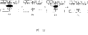
Discharge with producing with different discharge mechanisms in initial maintenance in normal time.For ease of describing, the discharge that is created in initial maintenance is called the short air gap discharge cycle, the discharge in normal time is called the long gap discharge cycle.
(3-1) short air gap discharge cycle
As (a) of Fig. 7 E with (b) shown in the part, apply positive potential pulse to the X electrode, (symbol of positive and negative is relative notion to the Y electrode to apply negative potential pulse, be used for relatively being applied to the intensity of the voltage of X and Y electrode, and applying positive pulse voltage represents to be higher than the voltage that is applied to the Y electrode voltage to the X electrode and is applied to the X electrode), and apply positive potential pulse simultaneously to the M electrode.Therefore, with wherein the regular situation that occurs between X electrode and the Y electrode of discharge is different, discharge occurs between X electrode/M electrode and the Y electrode.Particularly, because M and Y distance between electrodes be less than X and Y distance between electrodes, therefore the electric field that is applied between M and the Y electrode becomes higher.Therefore, compare with the Y electric discharge between electrodes, play a major role at M and Y electric discharge between electrodes with X.As mentioned above, in keeping early, play topmost effect having more short-range relatively M and Y electric discharge between electrodes, this is called the short air gap discharge.
Therefore, when applying first behind the addressing period when in discharge cell, producing not enough starting particle when keeping pulse, owing to, make the short air gap discharge generation of in the maintenance stage early, carrying out, thereby finish sufficient discharge by applying high relatively electric field.
(3-2) the long gap discharge cycle
Since apply keep first keep pulse after, voltage with fixed voltage Vm biasing M electrode, between M and X electrode or (for example in M and Y electric discharge between electrodes, the short air gap discharge) plays less important effect, become main discharge at X and Y electric discharge between electrodes, show input picture by a series of discharge pulses that alternately are applied to X and Y electrode.
That is to say that shown in the part (d) of Fig. 7 E, normally keeping the cycle, negative wall electric charge continues to accumulate in the M electrode, and negative wall electric charge and positive wall electric charge alternately gather X and Y electrode.
Because carry out discharge at (or between Y and M electrode) between X and the M electrode by the short air gap discharge in the maintenance stage early, carry out sufficient discharge at the starting particle more after a little while, and because in normal state, between X and Y electrode, carry out discharge, thereby carry out stable discharge by long gap discharge.
In addition, because the voltage waveform that applies almost symmetry is to X and Y electrode, become much at one pattern being used to drive the circuit design of X with the Y electrode.Therefore, because the circuit impedance difference almost has been eliminated between X and Y electrode, reduces so in the cycle of keeping, be applied to the distortion of the pulse waveform of X and Y electrode, and stable discharge is provided.
According to first exemplary embodiment as shown in Figure 6, can drive the inversion waveforms of X and Y electrode, also can in addressing period, drive the inversion waveforms of X and Y electrode.
According to the driving method of first exemplary embodiment, mainly apply reset wave and scanning impulse waveform to the M electrode, and mainly apply and keep voltage waveform to X and Y electrode.In this case, can apply various types of reset waves and reset wave as shown in Figure 6 to the M electrode.
To 7E and Fig. 8, the driving method according to second exemplary embodiment of the present invention will be described with reference to figure 7A.Fig. 8 has shown the drive waveforms figure according to the plasma scope of second exemplary embodiment of the present invention.
Each subdomain comprises the reset cycle, addressing period and keeping the cycle because addressing and keep the description in cycle and driving method as shown in Figure 6 similar, the description of repetition will be provided.
Reset cycle according to second exemplary embodiment comprises the removing cycle, and the M electrode rises/unsteady (floating) wave period and M electrode decline/unsteady wave period.
(1) the removing cycle
This cycle is used for removing the wall electric charge that the former cycle of keeping forms.Suppose that in second exemplary embodiment in the back part in the cycle of keeping, apply and keep potential pulse to the X electrode and apply ground voltage to the Y electrode, positive wall accumulation is at Y and address electrode, and negative wall electric charge is formed on X and M electrode.
During the removing cycle, apply drop to ground voltage gradually from voltage Vmc waveform (ramp waveform or logarithm waveform) to the M electrode, the Y of working voltage Vyc biasing simultaneously electrode.Therefore, shown in Fig. 7 A, the wall electric charge that forms during the cycle of keeping is eliminated.
(2) the M electrode rises/unsteady wave period
During this cycle, apply the rising/waveform that floats to the M electrode, use the voltage bias X and the Y electrode of ground voltage simultaneously, the waveform that wherein rises/float is used for repeating to apply the rising waveform from voltage Vmd to voltage Vset and carrying out and float.When applying the rising/waveform that floats, in whole discharge cells, produced faint discharge to X and Y electrode from the M electrode.More detailedly be, when applying rising waveform to the M electrode, resetting occurs in whole discharge cells to gather the wall electric charge, and the M electrode is floated, and the discharge in discharge space has been eliminated in fact.As a result, shown in Fig. 7 B, negative wall accumulation is at the M electrode, and positive wall electric charge accumulates in X and Y electrode simultaneously.
(3) the M electrode descends/unsteady wave period
In the back part of reset cycle, apply the decline/waveform that floats to the M electrode, with voltage Vxe, Vye setover respectively X and Y electrode, the waveform that wherein descends/float is used to repeat to apply the falling waveform from voltage Vme to ground voltage and carry out unsteady simultaneously.When applying the decline/waveform that floats, in whole discharge cells, produced faint discharge.
As applying the result of decline/unsteady waveform to the M electrode, the wall electric charge that accumulates in each electrode of whole unit is removed by unified, and shown in Fig. 7 C, positive wall accumulation is to address electrode, and negative wall electric charge gathers X, Y and M electrode simultaneously.
Except that the waveform that applies shown in Fig. 6 and 8, can apply various types of reset waves of three-electrode structure that are used for to the M electrode.Owing to readily understanding from the above description various types of reset waves are applied to four electrode structures, therefore corresponding description is not provided by those skilled in the art.
According to exemplary embodiment of the present invention, when using various types of reset waves, preferably satisfy four conditions that propose below to four electrode structures.
The first, in the reset wave that rises the cycle, be applied to the M electrode voltage waveform Rm (v) be set to be higher than the voltage waveform Rx that is applied to the X electrode (v) or be applied to the Y electrode voltage waveform Ry (v) (that is, Rm (v)>(Rx (v) or Ry (v)).
The second, in the reset wave that descends the cycle, be applied to the M electrode voltage waveform Fm (v) be set to be lower than the voltage waveform Fx that is applied to the X electrode (v) or be applied to the Y electrode voltage waveform Fy (v) (that is, Fm (v)<(Fx (v) or Fy (v)).
The 3rd, in addressing period, be applied to the M electrode voltage waveform Am (v) be set to be lower than the voltage waveform Ax that is applied to the X electrode (v) or be applied to the Y electrode voltage waveform Ay (v) (that is, Am (v)<(Ax (v) or Ay (v)).
The 4th, in the cycle of keeping, be applied to the M electrode voltage waveform Sm (v) be set to be higher than the voltage waveform Sx that is applied to the X electrode (v) or be applied to the Y electrode voltage waveform Sy (v) (that is, Sm (v)>(Sx (v) or Sy (v)).In addition, be applied in the cycle of keeping the voltage waveform Sm of M electrode (v) be set to be higher than the voltage waveform Am that in addressing period, is applied to the M electrode (v) (that is, Sm (v)>Am (v)).
Fig. 9 has shown the plasma scope figure according to first exemplary embodiment of the present invention.
As shown in the figure, plasma scope comprises plasma display panel 100, address driver 200, Y electrode driver 300, X electrode driver 400, M electrode driver 500 and controller 600.
Can on a side of plasma display panel, provide Y electrode driver 300.X electrode driver 400 can be provided on its opposite side.In first exemplary embodiment, can on its predetermined side (for example, on the residing side of X electrode driver), provide M electrode driver 500 as Fig. 8.That is to say, whole M electrodes are coupled to the M electrode driver 500 that provides on the side of plasma display panel.
Figure 10 has shown the electrode spread figure according to first exemplary embodiment of the present invention.As shown in the figure, with the M electrode spread between Y and X electrode.For ease of describing, when being provided for driving the driver of X, Y and M electrode, on this position, provide reference number.Promptly, the reference number of the driver that is used to drive the Y electrode is added in the left side of Y electrode, this is because provide driver in its left side, and the reference number of the driver that is used to drive X and M electrode is added in the right side of X and M electrode, and this is because provide driver on its right side.
In above-mentioned electrode arranging structure, suppose that the direction of scanning is from top to bottom on display board, during addressing period, the M electrode under the situation of single scanning with M1, M2, M3 ..., the order of MM1, MM2, MM3, and the order with (M1, MM1), (M2, MM2), (M3, MM3) scans under two scan condition.
Because the M electrode is coupled to the M electrode driver 500 that the side at display board provides, when needs are used to obtain high-resolution many electrode, the M electrode that is used to be coupled increases to the terminal cable of M electrode driver, therefore, and the gap turn narrow between the coupling terminal cable.Therefore, when the number that increases electrode when obtaining the high resolving power of the plasma scope of first exemplary embodiment according to the present invention, have difficulty the M electrode be coupled to M electrode driver 500.
Figure 11 and 12 has shown according to the present invention the plasma scope figure and the electrode spread figure of second exemplary embodiment respectively.As shown in figure 11, plasma scope comprises plasma display panel 100, address driver 200, Y electrode driver 300, X electrode driver 400, a M electrode driver 520, the 2nd M electrode driver 540 and controller 600 '.
Be provided for driving respectively first and second electrode drivers 520,540 of odd lines and even lines M electrode in the both sides of plasma display panel 100.The parts of carrying out Figure 11 of identical function and operation with those parts of Fig. 9 have identical reference number, and the description of repetition is not provided.
The one M electrode driver 520 is coupled to odd lines M electrode, receives the M electrode drive signal SM1 that is used to drive odd lines M electrode of self-controller 600 ', and it is applied to the M electrode.The 2nd M electrode driver 540 is coupled to even lines M electrode, receives the M electrode drive signal SM2 that is used to drive even lines M electrode of self-controller 600 ', and it is applied to the M electrode.In this case, be preferably in a M electrode driver 520 and X electrode driver 400, the 2nd M electrode driver 540 and Y electrode driver 300 are provided respectively on the same PCB.
Because a M electrode driver 520 that provides on the side of flat board (panel) is provided odd lines M electrode, and the 2nd M electrode driver 540 that provides on the dull and stereotyped opposite side is provided even lines M electrode, therefore when many M electrodes of needs during with the acquisition high resolving power, the gap of the terminal cable of odd lines M electrode to the M electrode driver that is used to be coupled (or terminal cable of even lines M electrode to the two M electrode drivers that are used to be coupled) becomes half of gap of the required terminal cable of first exemplary embodiment of Fig. 9.
Therefore, when the number that increases electrode when obtaining high resolving power, in plasma scope, can easily carry out the terminal coupling according to second exemplary embodiment.
In the electrode arranging structure of Figure 11 and 12, the scanning sequency of the M electrode in addressing period is as follows.
At first, under the situation of single scanning the M electrode with ML1, ML2, ML3 ..., the sequential scanning of MR1, MR2, MR3.In this case, owing to scan the direction of the direction of odd number M electrode corresponding to scanning even number M electrode, therefore dull and stereotyped flash-over characteristic is may not can even.
Therefore, when considering dull and stereotyped flash-over characteristic, under the situation of single scanning with ML1, ML2, ML3 ..., the sequential scanning M electrode (that is, the direction of line sweep odd number M electrode is set to opposite with the direction of line sweep even number M electrode) of MR3, MR2, MR1 is favourable.
Under two scan condition, the M electrode with (ML1, MML1), (ML2, MML2) ..., the order of (MR2, MMR2), (MR1, MMR1) or with (ML1, MML1), (ML2, MML2) ..., the sequential scanning of (MR1, MMR1), (MR2, MMR2).
Odd lines M electrode and even lines M electrode are coupled to a M electrode driver 520 and the 2nd M electrode driver 540 that on the right side of plasma display panel and left side, provides respectively, in addition, by the whole bag of tricks the M electrode is divided into a plurality of groups, and each group is coupled to the first and second M electrode drivers 520 and 540.
Figure 13 and 14 has shown according to the present invention skeleton view and the cross-sectional view of the PDP of first exemplary embodiment respectively.With reference to Figure 13 and 14, plasma display panel comprises first substrate 41 and second substrate 42.X electrode 53 and Y electrode 54 are formed on first substrate 41.Bus electrode 46 is formed on X and the Y electrode 53,54.Dielectric layer 44 and diaphragm 45 orders are formed on X and the Y electrode 53,54.
In plasma display panel, providing M electrode between Xi electrode and the Yi electrode and between Xi+1 electrode and Yi+1 electrode according to first exemplary embodiment of the present invention.That is to say, when (n/2+1) individual X and Y electrode are provided, provide n M electrode.
In addition, as shown in figure 15, can be between Xi electrode 53 and Yi electrode 54, and between Yi electrode and Xi+1 electrode, do not provide M electrode 56.In this case, the number of X, Y and M electrode is n.
Figure 16 has shown according to the present invention the partial plan of the PDP of second exemplary embodiment, and Figure 17 has shown the partial cross sectional view about the line A-A of Figure 16.Plasma display panel comprises first substrate 100 and second substrate 200.A plurality of address electrodes 210 are formed on second substrate 200 along a direction (y direction of principal axis), and a plurality of X electrodes 130 and Y electrode 140 are formed on first substrate 100 along the direction (x direction of principal axis) perpendicular to address electrode 210 directions.X and Y electrode 130,140 are corresponding with each discharge cell 270 in couples.Dielectric layer 70 and diaphragm 80 orders are formed on first substrate 100, and cover X and Y electrode 130,140.Dielectric layer 230 is formed on second substrate 200, and overlay address electrode 210.
A plurality of barrier ribs 150 are formed between first and second substrates 100,200.Barrier ribs 150 is arranged between the adjacent address electrode 210 and parallel, and forms the required discharge cell 270 of plasma discharge with address electrode 210.
Be used to form X electrode 130 and the Y electrode 140 of keeping electrode and comprise projected electrode 130a, 140a and bus electrode 130b, 140b separately.Projected electrode 130a, 140a are used for producing plasma discharge in discharge cell 270, preferably transparent indium tin oxide (ITO) electrode is applied to projected electrode 130a, 140a to obtain brightness, and preferably metal electrode is applied to bus electrode 130b, 140b, thereby compensates the high impedance of transparency electrode and obtain electric conductivity.Form a pair of bus electrode 130b, 140b abreast corresponding to each discharge cell 270, and with projected electrode 130a, 140a from each bus electrode 130b, 140b towards each discharge cell 270 projection so that they can be toward each other.
As shown in figure 16, spill (concave) unit B is formed on the central authorities of projected electrode 130a, 140a, smooth (flat) unit C is formed on the both sides of concave unit B.The length d 2 of M electrode middle body will be longer than the length d 1 of its marginal portion, and wherein middle body is corresponding to the concave unit B of projected electrode 130a, 140a.Calculated address electrode 210 is superimposed upon on the middle body of the concave unit B of projected electrode and M electrode.
Short air gap SG is formed between M electrode 180 and each projected electrode 130a, the 140a.Long gap L G is formed between the projected electrode.Main discharge begins to long gap so that expand to whole discharge cell 270 from initial short air gap.
The length L G2 in the long gap between the concave unit B of projected electrode 130a, 140a is greater than the length L G1 in the long gap between the concave unit B.Have relative big area owing to produce the address electrode of address with the zone that the M electrode is joined, therefore the electrode structure according to second exemplary embodiment has more excellent addressing efficient.In addition, owing to can shorten distance L G1 that form, that be used to keep between the planar unit mode C of projected electrode 130a, 140a, keep the voltage reduction thereby make.
As mentioned above, concave unit B and planar unit mode C are formed on projected electrode 130a, the 140a that arranges on the side of keeping electrode 130,140, or on the projected electrode 130a, the 140a that arrange on the both sides of keeping electrode 130,140.In addition, shown in Figure 18 A and 18B, the structure of projected electrode 130a, 140a and M electrode 180 is inequality.
In addition,, apply reset wave and sweep waveform, and apply and keep voltage waveform, prevented the inefficacy of discharging to X and Y electrode to the M electrode by between X and Y electrode, forming the M electrode.
Although represented with reference to definite preferred embodiment of the present invention and described the present invention, but the one of ordinary skilled in the art will be appreciated that and can be under the prerequisite that does not deviate from the aim of the present invention that limited by appended claims and scope the present invention be carried out modification on various forms and the details.
Claims (29)
1. method that is used to drive plasma scope, described plasma scope comprises and is used for receiving respectively first electrode and second electrode of keeping potential pulse, and be formed on third electrode between each first electrode and second electrode, this method comprises:
(a) during reset time interval, apply from the 5th voltage and drop to the falling waveform of the 6th voltage to third electrode;
(b) during the period 1 at interval of holding time, between first electrode and third electrode, carry out the short air gap discharge; And
(c) during the second round at interval of holding time, executive chairman's gap discharge between first electrode and second electrode.
2. the method for claim 1 wherein produces first and keeps during the period 1.
3. method as claimed in claim 2, wherein be the time interval that provides after first keeps second round.
4. the method for claim 1 wherein during the addressing time interval, applies scan pulse voltage to third electrode.
5. the method for claim 1 wherein during the addressing time interval, applies first voltage to first electrode, and apply be higher than first voltage second voltage to second electrode.
6. method as claimed in claim 5 is wherein carried out short air gap discharge and is comprised applying respectively and keep pulse and tertiary voltage to first electrode and second electrode, and apply be higher than tertiary voltage the 4th voltage to third electrode.
7. method as claimed in claim 6, wherein executive chairman's gap discharge comprises alternately applying and keeps pulse to first electrode and second electrode, and by the 4th voltage bias tertiary voltage.
8. method as claimed in claim 5, wherein first voltage is ground voltage.
9. method as claimed in claim 6, wherein tertiary voltage is a ground voltage.
10. one kind is used to drive the plasma scope method, and described plasma scope comprises first electrode and second electrode and be formed on third electrode between each first electrode and second electrode that described method comprises:
(a) during reset time interval, apply from the 5th voltage and drop to the falling waveform of the 6th voltage to third electrode; And
(b) alternately apply in the interim of holding time and keep potential pulse to first electrode and second electrode.
11. method as claimed in claim 10 wherein in reset time interval with during the addressing time interval that provides between holding time at interval, applies scan pulse voltage to third electrode.
12. method as claimed in claim 11 wherein applies first voltage to first electrode during the addressing time interval, and apply be higher than first voltage second voltage to second electrode.
13. method as claimed in claim 12 wherein applies respectively during the period 1 of holding time at interval and keeps pulse and tertiary voltage to first electrode and second electrode, and apply be higher than tertiary voltage the 4th voltage to third electrode.
14. method as claimed in claim 13 wherein produces first and keeps during the period 1.
15. method as claimed in claim 13 wherein during the second round at interval of holding time, alternately applies and keeps pulse to first electrode and second electrode, and by the 4th voltage bias third electrode.
16. method as claimed in claim 10 further comprises:
Applying falling waveform before the third electrode,
Apply removing voltage to third electrode in reset time interval; And
Apply from first voltage and rise to the rising waveform of second voltage to third electrode.
17. method that is used to drive plasma scope, described plasma scope comprises and is used for receiving respectively first electrode and second electrode of keeping potential pulse and is formed on third electrode between each first electrode and second electrode, wherein comprises in reset time interval:
(a) apply removing voltage to third electrode;
(b) apply from first voltage and rise to the rising waveform of second voltage to third electrode; And
(c) apply from tertiary voltage and drop to the falling waveform of the 4th voltage to third electrode.
18. method as claimed in claim 17 wherein applies removing voltage and comprises:
Apply from the 5th voltage and drop to the falling waveform of the 6th voltage to third electrode;
By the 7th voltage bias first electrode that is lower than the 5th voltage; And
By the 8th voltage bias second electrode that is higher than the 7th voltage.
19. method as claimed in claim 18, wherein holding time interim of subdomain formerly applies and keeps voltage at last to first electrode.
20. method as claimed in claim 17 wherein applies rising waveform and comprises: apply the rising/waveform that floats, what be used for the repetition rising waveform applies and floats to third electrode.
21. method as claimed in claim 17 wherein applies falling waveform and comprises: apply the decline/waveform that floats, what be used for the repetition falling waveform applies and floats to third electrode.
22. a method that is used to drive plasma scope, described plasma scope comprise first and second electrodes and are formed on third electrode between each first electrode and second electrode, comprising:
(a) during reset time interval, apply from the 5th voltage and drop to the falling waveform of the 6th voltage to third electrode;
(b) during the addressing time interval, apply scanning impulse to third electrode; And
(c) holding time interim, alternately applying and keep potential pulse to first electrode and second electrode.
23. method as claimed in claim 22 wherein in reset time interval with during the addressing time interval that provides between holding time at interval, applies scanning impulse to third electrode.
24. method as claimed in claim 23 wherein during the addressing time interval, applies first voltage to first electrode, and apply be higher than first voltage second voltage to second electrode.
25. method as claimed in claim 24 wherein during the period 1 of holding time at interval, applies respectively and keeps pulse and tertiary voltage to first electrode and second electrode, and apply be higher than tertiary voltage the 4th voltage to third electrode.
26. method as claimed in claim 25 wherein produces first and keeps during the period 1.
27. method as claimed in claim 25 wherein during the second round at interval of holding time, alternately applies and keeps pulse to first electrode and second electrode, and by the 4th voltage bias third electrode.
28. a method that is used to drive plasma scope, described plasma scope comprise first electrode and second electrode and are formed on third electrode between each first electrode and second electrode, comprising:
(a) during reset time interval, apply from the 5th voltage and drop to the falling waveform of the 6th voltage to third electrode;
(b) during the addressing time interval, apply first voltage to first electrode, and apply be higher than first voltage second voltage to second electrode; And
(c) during first cycle of keeping of holding time at interval, apply tertiary voltage to first electrode, apply be lower than tertiary voltage the 4th voltage to second electrode, and apply be higher than one of the first and the 4th voltage the 5th voltage to third electrode.
29. method as claimed in claim 28 wherein applies scanning impulse to third electrode during the addressing time interval.
Applications Claiming Priority (3)
| Application Number | Priority Date | Filing Date | Title |
|---|---|---|---|
| KR10-2003-0085465A KR100529114B1 (en) | 2003-11-28 | 2003-11-28 | A plasma display device and a driving method of the same |
| KR0085465/03 | 2003-11-28 | ||
| KR0085465/2003 | 2003-11-28 |
Publications (2)
| Publication Number | Publication Date |
|---|---|
| CN1637806A CN1637806A (en) | 2005-07-13 |
| CN100369088C true CN100369088C (en) | 2008-02-13 |
Family
ID=34464768
Family Applications (1)
| Application Number | Title | Priority Date | Filing Date |
|---|---|---|---|
| CNB200410095450XA Expired - Fee Related CN100369088C (en) | 2003-11-28 | 2004-11-29 | Plasma display and driving method thereof |
Country Status (5)
| Country | Link |
|---|---|
| US (1) | US7616176B2 (en) |
| EP (1) | EP1536403A3 (en) |
| JP (1) | JP2005165267A (en) |
| KR (1) | KR100529114B1 (en) |
| CN (1) | CN100369088C (en) |
Families Citing this family (9)
| Publication number | Priority date | Publication date | Assignee | Title |
|---|---|---|---|---|
| KR100637456B1 (en) * | 2004-02-05 | 2006-10-20 | 삼성에스디아이 주식회사 | Plasma display panel |
| KR100537624B1 (en) * | 2004-06-30 | 2005-12-19 | 삼성에스디아이 주식회사 | Method for operating four-electrode discharge display panel |
| JP4713170B2 (en) * | 2005-01-28 | 2011-06-29 | 日立プラズマディスプレイ株式会社 | Plasma display device and driving method thereof |
| JP2006235106A (en) * | 2005-02-23 | 2006-09-07 | Fujitsu Hitachi Plasma Display Ltd | Plasma display device |
| KR100659128B1 (en) * | 2005-12-21 | 2006-12-19 | 삼성에스디아이 주식회사 | Apparatus of driving plasma display panel and method thereof |
| WO2007088601A1 (en) * | 2006-02-01 | 2007-08-09 | Fujitsu Hitachi Plasma Display Limited | Method for driving plasma display device and plasma display device |
| JPWO2007088607A1 (en) * | 2006-02-01 | 2009-06-25 | 日立プラズマディスプレイ株式会社 | Plasma display panel driving method and plasma display apparatus |
| KR100766747B1 (en) * | 2006-03-23 | 2007-10-12 | 한국과학기술원 | Driving Method for AC Plasma Display Panel with 4 electrods, and AC PDP using this driving method |
| JP2007286192A (en) * | 2006-04-13 | 2007-11-01 | Fujitsu Hitachi Plasma Display Ltd | Method of driving plasma display panel |
Citations (4)
| Publication number | Priority date | Publication date | Assignee | Title |
|---|---|---|---|---|
| CN1349242A (en) * | 2000-07-05 | 2002-05-15 | Lg电子株式会社 | Plasma display panel, method and device for driving same |
| US20020084953A1 (en) * | 2000-12-28 | 2002-07-04 | Lg Electronics Inc. | Plasma display panel and driving method thereof |
| US6504519B1 (en) * | 1998-11-16 | 2003-01-07 | Lg Electronics, Inc. | Plasma display panel and apparatus and method of driving the same |
| US20030090443A1 (en) * | 2001-11-09 | 2003-05-15 | Pioneer Corporation | Plasma display panel and method of driving same |
Family Cites Families (16)
| Publication number | Priority date | Publication date | Assignee | Title |
|---|---|---|---|---|
| JPH09245627A (en) | 1996-03-07 | 1997-09-19 | Mitsubishi Electric Corp | Gas discharge display device, manufacture thereof and drive method of panel thereof |
| KR19980046358A (en) * | 1996-12-12 | 1998-09-15 | 엄길용 | Plasma Display Panel Structure and Its Driving Method |
| JP3818715B2 (en) | 1997-01-16 | 2006-09-06 | 株式会社日立製作所 | Display discharge tube |
| JPH1185098A (en) * | 1997-09-01 | 1999-03-30 | Fujitsu Ltd | Plasma display device |
| KR100319095B1 (en) | 1999-03-02 | 2002-01-04 | 김순택 | A plasma display panel having subsidiary electrodes and a driving method therefor |
| US7227513B2 (en) * | 1999-11-15 | 2007-06-05 | Lg Electronics Inc | Plasma display and driving method thereof |
| JP3728471B2 (en) * | 2000-02-07 | 2005-12-21 | パイオニア株式会社 | AC type plasma display, driving apparatus and driving method thereof |
| KR100366091B1 (en) | 2000-09-15 | 2002-12-26 | 삼성에스디아이 주식회사 | Plasma display panel having assistance electrode for reset, and drive method therefor |
| JP2002110047A (en) * | 2000-09-29 | 2002-04-12 | Fujitsu Hitachi Plasma Display Ltd | Plasma display device |
| KR20020035699A (en) * | 2000-11-07 | 2002-05-15 | 구자홍 | Plasma display panel and driving method thereof |
| JP2002175043A (en) * | 2000-12-06 | 2002-06-21 | Nec Corp | Method for driving plasma display panel, and circuit and display device thereof |
| KR100751931B1 (en) * | 2000-12-30 | 2007-08-24 | 엘지전자 주식회사 | Plasma Display Panel and Driving Method thereof |
| US6791516B2 (en) * | 2001-01-18 | 2004-09-14 | Lg Electronics Inc. | Method and apparatus for providing a gray level in a plasma display panel |
| DE10162258A1 (en) | 2001-03-23 | 2002-09-26 | Samsung Sdi Co | Operating plasma display involves inhibiting reset discharge in cells in which address discharge can occur in address interval, allowing reset discharge in cells without this characteristic |
| FR2826166B1 (en) * | 2001-06-13 | 2003-08-29 | Thomson Plasma | METHOD FOR CONTROLLING A PLASMA PANEL WITH CO-PLANAR MAINTENANCE DISCHARGES BETWEEN TRIADED ELECTRODES |
| JP4140685B2 (en) * | 2001-12-14 | 2008-08-27 | 株式会社日立製作所 | Plasma display panel |
-
2003
- 2003-11-28 KR KR10-2003-0085465A patent/KR100529114B1/en not_active IP Right Cessation
-
2004
- 2004-08-31 JP JP2004252102A patent/JP2005165267A/en active Pending
- 2004-11-26 EP EP04090470A patent/EP1536403A3/en not_active Withdrawn
- 2004-11-29 US US10/998,469 patent/US7616176B2/en not_active Expired - Fee Related
- 2004-11-29 CN CNB200410095450XA patent/CN100369088C/en not_active Expired - Fee Related
Patent Citations (4)
| Publication number | Priority date | Publication date | Assignee | Title |
|---|---|---|---|---|
| US6504519B1 (en) * | 1998-11-16 | 2003-01-07 | Lg Electronics, Inc. | Plasma display panel and apparatus and method of driving the same |
| CN1349242A (en) * | 2000-07-05 | 2002-05-15 | Lg电子株式会社 | Plasma display panel, method and device for driving same |
| US20020084953A1 (en) * | 2000-12-28 | 2002-07-04 | Lg Electronics Inc. | Plasma display panel and driving method thereof |
| US20030090443A1 (en) * | 2001-11-09 | 2003-05-15 | Pioneer Corporation | Plasma display panel and method of driving same |
Also Published As
| Publication number | Publication date |
|---|---|
| US7616176B2 (en) | 2009-11-10 |
| US20050140589A1 (en) | 2005-06-30 |
| EP1536403A2 (en) | 2005-06-01 |
| JP2005165267A (en) | 2005-06-23 |
| CN1637806A (en) | 2005-07-13 |
| KR100529114B1 (en) | 2005-11-15 |
| EP1536403A3 (en) | 2005-08-31 |
| KR20050051809A (en) | 2005-06-02 |
Similar Documents
| Publication | Publication Date | Title |
|---|---|---|
| US7561148B2 (en) | Plasma display panel driving method | |
| CN100361171C (en) | Plasma display device | |
| US7212176B2 (en) | Plasma display and driving method thereof | |
| CN100369088C (en) | Plasma display and driving method thereof | |
| CN100403364C (en) | Plasma display panel and driving method therefor | |
| US7030839B2 (en) | Method for driving plasma display panel and plasma display panel | |
| KR100589316B1 (en) | A plasma display device and a driving method of the same | |
| US8325110B2 (en) | Power supply and driver for plasma display panel | |
| KR100578960B1 (en) | Plasma display panel and driving method thereof | |
| CN100392704C (en) | Method of driving a plama display device | |
| US7592978B2 (en) | Plasma display panel driving method | |
| KR100420021B1 (en) | A driving apparatus of plasma display panel and the method thereof | |
| KR100477968B1 (en) | Method for driving plasma display panel | |
| US7499005B2 (en) | Plasma display panel and driving method thereof | |
| US20050110708A1 (en) | Plasma display panel and driving method thereof | |
| KR100560478B1 (en) | Plasma display device and driving method of the same | |
| KR100560473B1 (en) | A plasma display device and a driving method of the same | |
| KR100508928B1 (en) | Plasma display panel and driving method of plasma display panel | |
| KR100649521B1 (en) | Plasma display device | |
| KR100590023B1 (en) | A plasma display device and a driving method of the same | |
| KR20040082801A (en) | Driving method for plasma display panel | |
| KR20100128082A (en) | Plasma display apparatus |
Legal Events
| Date | Code | Title | Description |
|---|---|---|---|
| C06 | Publication | ||
| PB01 | Publication | ||
| C10 | Entry into substantive examination | ||
| SE01 | Entry into force of request for substantive examination | ||
| C14 | Grant of patent or utility model | ||
| GR01 | Patent grant | ||
| C17 | Cessation of patent right | ||
| CF01 | Termination of patent right due to non-payment of annual fee |
Granted publication date: 20080213 Termination date: 20131129 |