CN100353557C - Semiconductor camera element of contrast strong detection power - Google Patents
Semiconductor camera element of contrast strong detection power Download PDFInfo
- Publication number
- CN100353557C CN100353557C CNB021432228A CN02143222A CN100353557C CN 100353557 C CN100353557 C CN 100353557C CN B021432228 A CNB021432228 A CN B021432228A CN 02143222 A CN02143222 A CN 02143222A CN 100353557 C CN100353557 C CN 100353557C
- Authority
- CN
- China
- Prior art keywords
- pixel
- node
- camera element
- semiconductor camera
- signal
- Prior art date
- Legal status (The legal status is an assumption and is not a legal conclusion. Google has not performed a legal analysis and makes no representation as to the accuracy of the status listed.)
- Expired - Fee Related
Links
- 239000004065 semiconductor Substances 0.000 title claims description 61
- 238000001514 detection method Methods 0.000 title claims description 18
- 230000003321 amplification Effects 0.000 claims abstract description 22
- 238000003199 nucleic acid amplification method Methods 0.000 claims abstract description 22
- 230000008878 coupling Effects 0.000 claims description 15
- 238000010168 coupling process Methods 0.000 claims description 15
- 238000005859 coupling reaction Methods 0.000 claims description 15
- 238000009792 diffusion process Methods 0.000 claims description 13
- 239000000758 substrate Substances 0.000 claims description 13
- 230000005669 field effect Effects 0.000 claims description 6
- 206010034960 Photophobia Diseases 0.000 abstract 1
- 208000013469 light sensitivity Diseases 0.000 abstract 1
- 230000015572 biosynthetic process Effects 0.000 description 37
- 238000010586 diagram Methods 0.000 description 20
- 230000035945 sensitivity Effects 0.000 description 17
- 230000006870 function Effects 0.000 description 11
- 230000002093 peripheral effect Effects 0.000 description 8
- 230000000007 visual effect Effects 0.000 description 8
- 230000008447 perception Effects 0.000 description 7
- XUIMIQQOPSSXEZ-UHFFFAOYSA-N Silicon Chemical compound [Si] XUIMIQQOPSSXEZ-UHFFFAOYSA-N 0.000 description 5
- 229910052710 silicon Inorganic materials 0.000 description 5
- 239000010703 silicon Substances 0.000 description 5
- 230000009471 action Effects 0.000 description 4
- 238000003491 array Methods 0.000 description 2
- 230000008901 benefit Effects 0.000 description 2
- 230000008859 change Effects 0.000 description 2
- 230000000295 complement effect Effects 0.000 description 2
- 238000005516 engineering process Methods 0.000 description 2
- 238000005286 illumination Methods 0.000 description 2
- 238000003384 imaging method Methods 0.000 description 2
- 239000012535 impurity Substances 0.000 description 2
- 238000012544 monitoring process Methods 0.000 description 2
- 230000004044 response Effects 0.000 description 2
- 230000004913 activation Effects 0.000 description 1
- 238000006243 chemical reaction Methods 0.000 description 1
- 230000005611 electricity Effects 0.000 description 1
- 230000007613 environmental effect Effects 0.000 description 1
- 229910044991 metal oxide Inorganic materials 0.000 description 1
- 150000004706 metal oxides Chemical class 0.000 description 1
- 230000001105 regulatory effect Effects 0.000 description 1
- 229920006395 saturated elastomer Polymers 0.000 description 1
- 230000001953 sensory effect Effects 0.000 description 1
Images


Classifications
-
- H—ELECTRICITY
- H01—ELECTRIC ELEMENTS
- H01L—SEMICONDUCTOR DEVICES NOT COVERED BY CLASS H10
- H01L27/00—Devices consisting of a plurality of semiconductor or other solid-state components formed in or on a common substrate
- H01L27/14—Devices consisting of a plurality of semiconductor or other solid-state components formed in or on a common substrate including semiconductor components sensitive to infrared radiation, light, electromagnetic radiation of shorter wavelength or corpuscular radiation and specially adapted either for the conversion of the energy of such radiation into electrical energy or for the control of electrical energy by such radiation
- H01L27/144—Devices controlled by radiation
- H01L27/146—Imager structures
- H01L27/14601—Structural or functional details thereof
- H01L27/14603—Special geometry or disposition of pixel-elements, address-lines or gate-electrodes
-
- H—ELECTRICITY
- H04—ELECTRIC COMMUNICATION TECHNIQUE
- H04N—PICTORIAL COMMUNICATION, e.g. TELEVISION
- H04N25/00—Circuitry of solid-state image sensors [SSIS]; Control thereof
- H04N25/50—Control of the SSIS exposure
- H04N25/57—Control of the dynamic range
- H04N25/59—Control of the dynamic range by controlling the amount of charge storable in the pixel, e.g. modification of the charge conversion ratio of the floating node capacitance
-
- H—ELECTRICITY
- H04—ELECTRIC COMMUNICATION TECHNIQUE
- H04N—PICTORIAL COMMUNICATION, e.g. TELEVISION
- H04N25/00—Circuitry of solid-state image sensors [SSIS]; Control thereof
- H04N25/70—SSIS architectures; Circuits associated therewith
- H04N25/76—Addressed sensors, e.g. MOS or CMOS sensors
- H04N25/77—Pixel circuitry, e.g. memories, A/D converters, pixel amplifiers, shared circuits or shared components
-
- H—ELECTRICITY
- H04—ELECTRIC COMMUNICATION TECHNIQUE
- H04N—PICTORIAL COMMUNICATION, e.g. TELEVISION
- H04N3/00—Scanning details of television systems; Combination thereof with generation of supply voltages
- H04N3/10—Scanning details of television systems; Combination thereof with generation of supply voltages by means not exclusively optical-mechanical
- H04N3/14—Scanning details of television systems; Combination thereof with generation of supply voltages by means not exclusively optical-mechanical by means of electrically scanned solid-state devices
- H04N3/15—Scanning details of television systems; Combination thereof with generation of supply voltages by means not exclusively optical-mechanical by means of electrically scanned solid-state devices for picture signal generation
- H04N3/155—Control of the image-sensor operation, e.g. image processing within the image-sensor
Abstract
Each pixel includes first and second photodiodes that are receiving-light detecting elements. The first photodiode applies a first potential according to an amount of light entering into the corresponding pixel. An internal node is electrically coupled with an internal node in another pixel via a resistance component. Hence, the second photodiode applies a second potential according to an average amount of light on the periphery to the corresponding internal node. A pixel signal generating circuit reads out a multiplied result of the first and second potentials as a pixel signal. The pixel signal has an intensity corresponding to the amount of light in the pixel in accordance with a receiving-light sensitivity characteristic (signal amplification factor) that is automatically adjusted based on an average amount of light in a region on the periphery of the pixel.
Description
Technical field
The present invention relates to realize the semiconductor camera element that be subjected to light perception characteristic approaching, especially be particularly related to and in the visual field, mix the semiconductor image sensor that exists the very big zone of difference in brightness also can detect enough contrasts in whole zone with people's vision perception characteristic.Thereby the technology of the present invention can be used as the camera head with high visually-perceptible ability that uses under various situations, can be used to comprise outdoor camera for monitoring and vehicle mounted video camera etc.
Background technology
Solid-state imagers such as charge coupled device (CCD:Charge-coupled device) and complementary type metal-oxide-semiconductor (CMOS:complementary metal-oxide semiconductor) imaging apparatus, be so-called semiconductor image sensor (below be also referred to as " semiconductor camera element "), from be contained in video camera and Digital camera, in the mobile phone etc. solid-state imager is housed also till now, it is extensively popularized as cheapness and the little imaging apparatus of power consumption.
But the perception of semiconductor camera element is significantly less than people's visually-perceptible ability.Even people's vision has the Luminance Distribution of 4-5 order of magnitude speed in a visual field, also can be enough to detect the contrast of bright place and dark place.This excellent contrast perception is to utilize to be in the intraretinal photo-cell that is subjected to and can the function that each cell is regulated its photobehavior to be realized.
Different therewith is, in semiconductor camera element in the past, because all pixels have the identical light characteristic that is subjected to, therefore is difficult to obtain simultaneously where there is light in the visual field and enough contrasts of dark place.
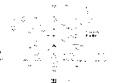
Figure 14 and the 1st figure and the 2nd figure that Figure 15 shows that the shooting example of utilization semiconductor camera element in the past.
With reference to Figure 14 and Figure 15, these take examples is outside window the sights of comprising from the indoor shot of lighting fluorescent lamp on sunny daytime.Such sight is the quotidian scene of often seeing in daily life.Common like this sight is in people's eye, and no matter indoor still outside window sight can see without difficulty that all such experience is all known with enough contrasts.
But with in the past semiconductor camera element, if shown in the shooting example of Figure 14, that adjusts pixel is subjected to the luminous sensitivity characteristic, makes to see indoorly, then bright excessively outside window, can not detect the contrast of light.In addition, if adjust shown in the shooting example of Figure 15, making and can see outside window sight with enough contrasts, then this time is indoor dark excessively, is difficult to detect the contrast of dark part.Hence one can see that, with imageing sensor in the past, mixes simultaneously in the visual field when having bright areas and dark area, and the ability that detects enough contrasts in whole zone is significantly less than people's vision-based detection.
Thereby for in the past the semiconductor camera element visual information checkout gear of people's vision instead, this contrast perception is low to be to want the big problem that must solve in practicality.
The low situation of Contrast Detection ability of semiconductor camera element in the past is described with Figure 16 below.
The outdoor illumination on general sunny daytime is about tens thousand of Luxs.And the indoor illumination intensity of fluorescent lamp lighting is about about 500 Luxs in the place of not incident of sunlight, in the dark is below 100 Luxs.Promptly in Figure 14 and shooting example shown in Figure 15, shown in the Luminance Distribution example in Figure 16, the Luminance Distribution of Luminance Distribution outside window and indoor dark part (part of face) represents that with mean value separately the difference of 2-3 the order of magnitude is arranged.
In the shooting example of Figure 14, for can the enough contrasts of perception at indoor brighter zone (below 500 Luxs), that sensitivity straight line as shown in figure 16 adjusts pixel like that be subjected to the luminous sensitivity characteristic.But, as mentioned above, in semiconductor camera element in the past, because all pixel has identical sensory characteristic.Therefore if take with such luminous sensitivity characteristic that is subjected to, then, be subjected to luminous sensitivity saturated fully to outside window light, become snow-white.In addition we know, even in dark part, the amplitude below 1/5 for whole can not obtain enough contrasts.Like this, with in the past semiconductor camera element, connect we daily run into a lot of scenes can not the enough contrasts of perception.
Summary of the invention
Also can be under the situation that Luminance Distribution is big in the visual field even the object of the invention is to be provided at the semiconductor camera element of enough Contrast Detection lights and dark part.
According to semiconductor camera element of the present invention, the a plurality of pixel circuits that comprise the composing images transducer, each described pixel circuit can be adjusted intrinsic signal amplification factor to each pixel, and is subjected to the average signal of light signal intrinsic detection is modulated by the multiplication factor of reading of light signal to pixel to comprise the proximity detection of pixel on every side.
Preferably pixel circuit has and can carry out electrical analogue modulated M OS transistor to magnificationfactor, this MOS transistor is used for signal reads amplification.
Particularly in such structure, the average light income signal around in pixel circuit is input to modulation MOS transistor magnificationfactor control grid.
Perhaps, preferably it is characterized in that, utilize the diode that between trap and substrate, forms with by being connected the average light income signal of resistance around providing between the pixel of trap shape set.
It is characterized in that preferably forming provides each pixel to be subjected to the photodiode of light signal in trap.
Semiconductor camera element according to other structure of the present invention, comprise a plurality of pixels, each pixel comprises image signal generating circuit, described image signal generating circuit is according to this pixel and be configured in other a plurality of pixels around this pixel around at least a portion the light quantity of pixel and adjust signal amplification factor, generates the signal of telecommunication corresponding with the incident light quantity of this pixel according to this signal amplification factor.
Preferably according to the average light quantity setting signal multiplication factor in the pixel around described.
In addition, preferably set the signal amplification factor separately of a plurality of pixels, make signal amplification factor in the zone that the average light quantity of pixel is little around described relatively greater than the big zone of average light quantity of pixel around described.
Perhaps preferably each pixel also comprise be connected electrically between the 1st voltage node of supplying with the 1st fixed voltage and the 1st node, generate the 1st of 1st current potential corresponding at described the 1st node and be subjected to photodetector with the incident light quantity that incides described this pixel, and be connected electrically between the 2nd voltage node of supplying with the 2nd fixed voltage and the 2nd node, generate the 2nd of 2nd current potential corresponding at described the 2nd node and be subjected to photodetector with the incident light quantity that incides described pixel on every side.Image signal generating circuit is according to the long-pending signal of telecommunication that generates of the 1st and the 2nd current potential.
Preferably for each described pixel, the 1st current potential rises along with the increase of the incident light quantity that incides described this pixel, and the 2nd current potential descends along with the increase of inciding the described incident light quantity of pixel on every side.
Perhaps preferably for each described pixel, the 1st current potential descends along with the increase of the incident light quantity that incides described this pixel, and the 2nd current potential rises along with the increase of inciding the described incident light quantity of pixel on every side.
In addition, the best the 1st be subjected to photodetector have with from the 1st node to the direction of described the 1st voltage node as positive direction, the 1st diode that between described the 1st voltage node and described the 1st node, is connected, the 2nd be subjected to the light detection elements have with from the 2nd voltage node to the direction of described the 2nd node as positive direction, the 2nd diode that between described the 2nd node and the 2nd voltage node, is connected.The 2nd node of pixel carries out electric coupling by resistance components each other around described.
In addition, the best the 1st be subjected to photodetector have with from the 1st voltage node to the direction of the 1st node as positive direction, the 1st diode that between the 1st voltage node and the 1st node, is connected, the 2nd be subjected to the light detection elements have with from the 2nd node to the direction of the 2nd voltage node as positive direction, the 2nd diode that between the 2nd node and the 2nd voltage node, is connected.The 2nd node of pixel carries out electric coupling by resistance components each other around described.
Perhaps, preferably image signal generating circuit comprises the field-effect transistor that can carry out analog-modulated according to the added voltage of control grid to magnificationfactor.The Control Node of field-effect transistor is connected with the 2nd node, and field-effect transistor amplifies the 1st node potential according to magnificationfactor, by such generation signal of telecommunication.
In addition, preferably semiconductor camera element also has the 1st and the 2nd node potential is reset to the reset circuit that the regulation current potential is used respectively with specified period.
Perhaps, preferably semiconductor camera element also has with specified period the 1st node potential is reset to the regulation current potential, simultaneously the reset circuit that the 2nd node is used by resistance components and fixing bias voltage electric coupling.
In addition, preferably semiconductor camera element generates on the 1st conductivity type substrate, also has the 2nd conductivity type well region of the conductivity type opposite with the 1st conductivity type that forms on substrate.The diode that the 2nd had by photodetector utilizes the knot between substrate and the well region to form.
Best the 2nd node is equivalent to well region.
Perhaps, preferably semiconductor camera element also has the 1st diffusion region of the 1st conductivity type that forms in well region, and the 2nd diffusion region of the 2nd conductivity type that forms in the 1st diffusion region.The the 1st and the 2nd diffusion region independently is provided with each pixel, the diode that the 1st had by photodetector utilizes the knot between the 1st diffusion region and the 2nd diffusion region to form.
Thereby major advantage of the present invention is, the image that big luminance difference is arranged in same visual field that can be difficult to detect with enough Contrast Detection usefulness imageing sensors in the past.As a result, semiconductor camera element of the present invention (imageing sensor) can be used as the camera head that has near the excellence of people's perceptibility.Thereby this imageing sensor can be exploited one's power in the field that requirements such as monitoring arrangement and vehicle-mounted vidicon adapt to rapid environmental change.
Because the S/N of general cmos image sensor ratio is for about 60-65dB, therefore if the picture quality of dark place allows for about 29dB in the picture, semiconductor camera element then of the present invention (imageing sensor) is estimated and can be detected enough contrasts in whole image, reaches the mean luminance differences about hundreds of times.
In addition, semiconductor camera element of the present invention (imageing sensor), owing to can be fitted together compactly by the function of luminous sensitivity characteristic with simulating each pixel to adjust, therefore compare with imageing sensor in the past, poor unlike it aspect sensitivity and definition.
Description of drawings
Figure 1 shows that formation schematic block diagram according to the semiconductor camera element of the embodiment of the invention.
The block diagram that Fig. 2 constitutes for each pixel of explanation.
Figure 3 shows that the detailed circuit diagram that each pixel constitutes.
Figure 4 shows that pixel characteristic schematic diagram and its shooting example according to semiconductor camera element of the present invention.
Figure 5 shows that the element of A-MOS device constitutes the schematic diagram of example.
Figure 6 shows that the element of A-MOS device constitutes the schematic diagram of parameter.
Fig. 7 A and 7B are the schematic diagram of explanation A-MOS device and β modulation principle.
Figure 8 shows that circuit diagram according to each pixel formation of embodiment 2.
Figure 9 shows that structure chart according to the photodiode configuration example of embodiment 3.
Figure 10 shows that circuit diagram according to each pixel formation of embodiment 4.
Figure 11 shows that circuit diagram according to each pixel formation of embodiment 5.
Figure 12 shows that structure chart according to the photodiode configuration example of embodiment 5.
Figure 13 shows that circuit diagram according to each pixel formation of embodiment 6.
Figure 14 shows that the 1st figure (indoor seeing) of the shooting example of utilization semiconductor camera element in the past.
Figure 15 shows that the 2nd figure (outdoor seeing) of the shooting example of utilization semiconductor camera element in the past.
Figure 16 is the low key diagram of Contrast Detection ability of semiconductor camera element in the past.
Embodiment
Below, embodiments of the present invention will be described in detail with reference to the accompanying drawings.In addition, in the following description, add same with reference to label to same or considerable part.
With reference to Fig. 1, semiconductor camera element 1 of the present invention comprises that a plurality of pixel PX are the cell array 2 of rectangular configuration, read-out control circuit 3, reset circuit 5 and power circuit 7.
View data in the read-out control circuit 3 formation object pixel array 2 generates the control signal RD that controls usefulness constantly.Reset circuit 5 regularly resets to the state that is subjected to photodetector among each pixel PX.The homing action that reset circuit 5 carries out is used to control from the reset signal Rst0 and the Rst1 of read-out control circuit 3 constantly.Each pixel supply line voltage Vd and earthed voltage GND in 7 pairs of cell arrays of power circuit 2.
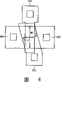
The block diagram that Fig. 2 constitutes for each pixel of explanation.In Fig. 2, provide as representative the capable and j row (i and j are natural number) of i in a plurality of pixels that are rectangular configuration pixel PX (i, j) and the group of pixels that is adjacent.
With reference to Fig. 2, each pixel PX comprises photodiode PD0 and the PD1 that is subjected to photodetector as conduct, pixel signal generative circuit 10 and pixel data generative circuit 15.
Photodiode PD1 generates the signal with current potential corresponding with this pixel incident light quantity.Photodiode PD0 is by the photodiode PD0 electric coupling in a plurality of pixels of resistance components and peripheral region.By like this, the photodiode PD0 of each pixel can generate the signal with current potential corresponding with the average light quantity of this pixel peripheral region.
In the formation example of Fig. 2, each pixel and adjacent 4 pixels between, photodiode PD0 electric coupling each other.For example pixel PX (i, j) with pixel PX (i, j+1), PX (i, j-1), PX (i-1, j) and PX (i+1, j) between electric coupling.But the application's invention is not limited to and is suitable for such formation, and the photodiode PD0 of each pixel can be connected with the photodiode PD0 of other pixel of any number that disposes on every side and constitute.
Pixel signal generative circuit 10 is according to the output separately of photodiode PD0 and PD1, the moment with control signal PD response generate with the corresponding picture signal of this pixel incident light quantity as output signal.Picture signal is according to according to the i.e. self-adjusting luminous sensitivity characteristic (signal amplification factor) that is subjected to of average light quantity of this pixel peripheral region of the output of photodiode PD0, has and the i.e. corresponding intensity of light quantity of this pixel of the output of photodiode PD1.
Thereby the luminous sensitivity characteristic that is subjected to of each pixel is adjusted automatically according to the average light quantity of this pixel peripheral region.Specifically, if in each pixel, set make this pixel be subjected to luminous sensitivity (signal amplification factor) and average light quantity or inverse ratio increase on every side.That is to say that each pixel has so automatic adjustment function, promptly setting is subjected to luminous sensitivity relatively large in the dark space, and setting is subjected to luminous sensitivity less relatively in the clear zone.
Pixel data generative circuit 15 carries out mould/number conversion with the output signal (pixel signal) of pixel signal generative circuit 10, generates view data DAT, and the view data that generates is temporarily preserved.The view data that view data generative circuit 15 keeps adopts not shown scanning circuit, can be unit with the pixel, the behavior unit of pixel, the unit of classifying as or whole cell arrays, from the semiconductor camera element outside to each arbitrarily scope read.In addition, in each not shown pixel, its internal structure and with the annexation between the pixel is all identical on every side.
Describe the formation of each pixel below in detail with Fig. 3.
With reference to Fig. 3, circuit is to constitute like this, the photodiode PD1 that promptly has the current potential Va that provides corresponding with the incident light quantity that incides pixel, and photodiode PD0 with the current potential Vb that average light quantity is corresponding on every side is provided, current potential Va that will be provided by each photodiode and the multiplied result of Vb are read as pixel signal.
Photodiode PD1 will be from node Na to the direction of supply voltage Vd as positive direction, be connected between node Na and the supply voltage Vd.Photodiode PD0 will be from earthed voltage GND to the direction of node Nb as positive direction, be connected between node Nb and the earthed voltage GND.
Resetting voltage Vt adds the voltage that the anti-bias voltage of regulation is used to photodiode PD1 when resetting, also can use earthed voltage GND.Simultaneously, resetting voltage Vdm adds the voltage that the anti-bias voltage of regulation is used to photodiode PD0 when resetting, and also can press Vd by electricity consumption piezoelectricity.About these bias voltages, for example can adopt the structure of supplying with by potential circuit shown in Figure 17.
Thereby, the homing action that utilizes reset circuit 5 to produce, (Vt Vdm) connects for node Na and Nb and assigned voltage.Then, in photodiode PD1 owing to produce the reverse current corresponding with the light quantity of this pixel, so corresponding generation time variation of light income of current potential Va and this pixel.
As described in Figure 2, the node Nb in each pixel is by the node Nb electric coupling in resistance components and other pixel.For example, in the formation of Fig. 3, pixel PX (i for example, j) the node Nb in by resistance components respectively with the pixel PX of upside (up) (i-1, j), the pixel PX (i+1 of downside (down), j), the pixel PX in left side (left) (i, j-1) and the pixel PX of right side (right) (i, internal node Nb electric coupling j+1).
Thereby the current potential of node Nb not only is subjected to the influence of the reverse current that the photodiode PD0 in this pixel produces, and also is subjected to the influence of the reverse current that the photodiode PD0 in other pixel of electric coupling produces, the generation time variation.Like this, by resistive component will around photodiode PD0 in the pixel connect each other, just can generate the current potential Vb that the light quantity on every side with this pixel be inversely proportional at node Nb.
Pixel signal generative circuit 10 has multiplier PU and reads selector switch transistor Tr 2.Multiplier PU generates the long-pending relevant current i with current potential Va separately and the Vb of node Na and Nb between node Nc and earthed voltage GND.It is multiplier.Be current characteristics formula i=f (Va * Vb) expression, the long-pending direct ratio that is approximated to of current i and current potential Va and Vb of multiplier PU.
Reading selector switch transistor Tr 2 exports the current potential of the node Nc of control signal RD activation moments as picture signal OUT.
By adopting such formation, even the current potential Va same level of node Na, in the promptly dark pixel partly of the pixel that average light quantity is few, the current potential of node Nc raises relatively around, and the pixel that average light quantity is many around is in the pixel of light, and the current potential of node Nc reduces relatively.Thereby the luminous sensitivity that is subjected to of each pixel increases and reduces in bright areas in dark area, has realized the signal amplification factor control of each such pixel.
Figure 4 shows that according to the pixel characteristic schematic diagram of semiconductor camera element of the present invention and the image of shooting example.
With reference to Fig. 4, in according to semiconductor camera element of the present invention, because each pixel has being subjected to the self-adjusting function of luminous sensitivity characteristic, thereby each pixel realized making sensitivity straight line (signal amplification factor) and average light quantity on every side in this pixel to be inversely proportional to changing such (the dark place increases multiplication factor more) adjusted function automatically.Have again, in having the semiconductor camera element of such function, if the whole pixels of adjustment are memory time (time for exposure) jointly, make it can keep enough contrasts for highlight in the visual field, then the signal owing to dark part amplifies according to the degree of darkness around it, therefore the contrast of dark part strengthens, and the Zone Full at picture just can detect enough contrasts like this.Time for exposure be equivalent to till reset signal Rst0 and Rst1 response carrying out homing action played control signal RD be activated during, set by read-out control circuit 3.Result's shooting example as shown in Figure 4 can be realized the semiconductor camera element that light and dark part can both detect with enough contrasts.
In embodiment 2, the formation of the multiplier PU that is fit to such signal amplification factor control is described.In embodiment 2, employing can according to control gate input voltage MOS transistor that magnificationfactor is controlled (below be also referred to as that " A-MOS (Adujustable β-MOS) device ") realizes each pixel is adjusted the function that is subjected to the luminous sensitivity characteristic automatically.
With reference to Fig. 5, the A-MOS device has the common grid G R identical with common MOS transistor, and in addition source S R and drain D R also have the control grid CG with the common angled form of grid.
Figure 6 shows that the element of A-MOS device constitutes the schematic diagram of parameter.
With reference to Fig. 6, the A-MOS device constitutes the long Lr of grid that parameter has common grid G R as element, the angle θ that forms between wide Wr of grid and common grid G R and the control grid CG.
Fig. 7 A and Fig. 7 B are the schematic diagram of β modulation principle in the explanation A-MOS device.
With reference to Fig. 7 A, when the channel conductivity under setting the feasible control of control grid CG institute's making alive grid CG was identical with common grid, the part among the figure shown in the hacures was effective gate regions.Promptly because effectively the long L of grid is longer than the long Lr of the grid of common grid G R, effectively the wide W of grid is narrower than the wide Wr of the grid of common grid G R, so magnificationfactor reduces.
In addition, with reference to Fig. 7 B, when the channel conductivity of setting the feasible control of control grid CG institute's making alive grid CGF was enough bigger than common grid, effectively wide W of grid and the long L of grid were with wide Wr of grid and the long Lr of grid of grid G R equate usually.
Like this, the A-MOS device can carry out analog-modulated to long L of effective grid and the wide W of grid by changing control grid CG institute making alive.As a result, the A-MOS device has realized utilizing the control gate pole tension to carry out the analog-modulated of magnificationfactor.Like this, the A-MOS device has the advantages that to realize the β modulating characteristic about 10-1000 times with compact structure.The modulating characteristic of the magnificationfactor of A-MOS device can utilize parameter shown in Figure 6 to set.
Figure 8 shows that circuit diagram according to each pixel formation of embodiment 2.
With reference to Fig. 8, in formation, the A-MOS transistor Tr 4 of electric coupling is set between node Nc and earthed voltage GND according to embodiment 2, replace multiplier PU.The common grid G R of A-MOS transistor Tr 4 is connected with node Na, and control grid CG is connected with node Nb.
Like this, formation in embodiment 2 is, the photodiode PD1 that corresponding current potential with the incident light quantity that incides pixel changes is connected with the common grid of A-MOS transistor Tr 4, is connected with the control grid of A-MOS transistor Tr 4 with the potential nodes Nb that average light quantity is corresponding on every side.As mentioned above, be to utilize the average light quantity detection that is connected with pixel on every side by resistive component to provide with average light quantity is corresponding on every side current potential with photodiode PD0.
Utilize this formation, in the promptly dark pixel partly of the pixel that average light quantity is few, increase the transistorized magnificationfactor of A-MOS on every side, the pixel to light reduces β, and each pixel has been realized such control.Call by name and talk about, utilize the A-MOS transistor, can realize the function of multiplier PU shown in Figure 3.
β by each such pixel adjusts, and identical with embodiment 1, the signal amplification factor of dark partial-pixel is greater than the pixel of light.As a result, can improve the contrast of dark place.Because it is identical with embodiment 1 that the other parts of reset circuit 5 and each pixel constitute, therefore do not repeat to describe in detail.
Like this, read amplifier transistor if adopt the A-MOS device as the signal of each pixel, then can provide the expression fairly simple like this circuit formation of voltage of average light quantity on every side with the control grid that needs only the A-MOS device, be implemented on every side when dark the multiplication factor of this pixel is improved about 100 times automatic adjustment function, can suppress to cause the increase of elemental area simultaneously owing to each pixel adds automatic adjustment function.
The following describes effective configuration of 2 photodiodes that each pixel is provided with in embodiment 3.
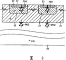
Figure 9 shows that structure chart according to the photodiode configuration example of embodiment 3.
With reference to Fig. 9, with the P type silicon substrate (P-sub) 20 that forms semiconductor camera element and and be arranged on the PN junction that forms between the N trap 21 on the P type silicon substrate 20, constitute and detect the photodiode PD0 that the peripheral region average light quantity is used.
Be used in the P that forms in this N trap 21 again
+ Type district 22 and with at P
+The N that forms in the type district 22
+The PN junction that forms between the type district 23 constitutes detection and incides the photodiode PD1 that the incident light quantity of this pixel is used.In addition, P
+Type district 22 and N
+The impurity concentration in type district 23 is higher than P type silicon substrate 20 and N trap 21.
P
+Type district 22 and N
+Type 23 is that each pixel independently is provided with.In addition, the diffusion resistance electric coupling by the N trap between a plurality of pixels that in same N trap 21, form, the node Nb during promptly the N trap 21 of each pixel circuit that is equivalent to Fig. 3 constitutes.Thereby between a plurality of pixels that same N trap 21 forms, node Nb electric coupling detects average light quantity.
Perhaps also can on same N trap, form whole cell array 2.In this case, in each pixel, the resistance value between the photodiode PD0 of this pixel and the photodiode PD0 of other pixel and the corresponding increase of distance of pixel value.Thereby, the current potential Vb of the node Nb in each pixel, because it is relatively large to be subjected to inciding the influence of incident light quantity of adjacent image point, so the result can detect the average light quantity of pixel peripheral region according to current potential Vb.
If according to the configuration of the photodiode of embodiment 3, then 2 of each pixel setting photodiodes dispose with vertical structure.Have again,, special wiring etc. can be set, with the shape formation of N trap for the connection of the resistance between the photodiode between pixel on every side.Thereby, can prevent the increase of each pixel and cell array area.
Embodiment 4
Figure 10 shows that circuit diagram according to the pixel formation of embodiment 4.
Figure 10 and Fig. 8 are compared, then in formation according to embodiment 4.Between resetting voltage (for example supply voltage Vd) and node Nb, be connected resistor R0, replace corresponding resetting of being provided with transistor Tr 0 with photodiode PD0.Therefore the formation of other parts does not repeat to describe in detail owing to identical with Fig. 8.
As such formation, since node Nb be stabilized in incide this pixel and with the corresponding current potential of incident light quantity of the photodiode PD0 in the pixel around this pixel electric coupling, therefore also the formation with embodiment 1 or 2 is identical, can utilize the average light quantity of the current potential Vb detection pixel peripheral region of node Nb.Thereby, for the detection action of average light quantity on every side,, therefore can simplify reset circuit 5 owing to do not need to carry out the reset operation of periodicity.In addition, same formation also can be suitable for for the circuit formation shown in Figure 3 according to embodiment 1.
Figure 11 shows that circuit diagram according to the pixel formation of embodiment 5.
Figure 11 and Fig. 8 are compared, and in the formation according to embodiment 5, are to exchange the configuration of photodiode according to the formation of embodiment 2.Be photodiode PD0 will be from node Nb to the direction of supply voltage vd as positive direction, be connected between node Nb and the supply voltage Vd, photodiode PD1 will be from earthed voltage GND to the direction of node Na as positive direction, be connected between earthed voltage GND and the node Na.Corresponding, read selector switch transistor Tr 2 and A-MOS transistor Tr 4 and make the N channel-type and change into the P channel-type.In addition, same formation also can be suitable for for the circuit formation shown in Figure 3 according to embodiment 1.
Figure 12 shows that structure chart according to the photodiode configuration example of embodiment 5.
With reference to Figure 12, in embodiment 5, use and be arranged on the PN junction that forms between the P trap 31 on the N type silicon substrate (N-sub) 30 that forms semiconductor camera element, constitute and detect the photodiode PD0 that pixel peripheral region average light quantity is used.Be used in the N that forms in this P trap 31 again
+ Type district 32 with at N
+The P that forms in the type district 32
+The PN junction that forms between the type district 33 constitutes detection and incides the photodiode PD1 that the incident light quantity of this pixel is used.
Identical with structure shown in Figure 9, N
+Type district 32 and P
+Type district 33 is that each pixel independently is provided with N
+The impurity concentration in type district 32 and P+ type district 33 is higher than N type silicon substrate 30 and P trap 31.In addition, about the design of P trap 31, as long as identical with N trap 21 among Fig. 9.
Like this, the formation that is exchanged as configuration with photodiode, also identical with embodiment 1 or 2, can be implemented in each pixel and the corresponding automatic adjustment function that sensitivity straight line (multiplication factor) is changed of average light quantity on every side, can detect enough contrasts in the whole image zone.Have again, identical with embodiment 3, in each pixel must the formation of 2 photodiodes, also can prevent the increase of each pixel and cell array area.
Embodiment 6
Figure 13 shows that circuit diagram according to the pixel formation of embodiment 6.
Figure 13 and Figure 11 are compared, in formation,, replace reset transistor Tr0 with the corresponding setting of photodiode PD0 being connected resistor R0 as between the earthed voltage GND of resetting voltage and the node Nb according to embodiment 6.Therefore the formation of other parts does not repeat to describe in detail owing to identical with Figure 11.
Like this, also identical in the formation that the configuration with photodiode is exchanged with embodiment 4, the formation of simplification reset circuit 5.And can detect enough contrasts in the whole image zone.In addition, in constituting according to the circuit of Figure 13, essential 2 the photodiode PD0 of each pixel are identical with the PD1 also structure chart with Figure 12, and its configuration can prevent the increase of each pixel and cell array area.
Claims (19)
1. a semiconductor camera element is characterized in that, comprises
A plurality of pixel circuits of composing images transducer,
Each described pixel circuit is adjusted intrinsic signal amplification factor to each described pixel circuit, and from comprising the average signal that the proximity detection of pixel on every side is subjected to light signal, intrinsic detection is modulated by the multiplication factor of reading of light signal to pixel.
2. semiconductor camera element as claimed in claim 1 is characterized in that,
Each described pixel circuit comprises and can carry out electrical analogue modulated M OS transistor to magnificationfactor, and described MOS transistor is used for signal and reads amplification.
3. semiconductor camera element as claimed in claim 2 is characterized in that,
In each described pixel circuit, average light income signal on every side is input to the control grid that the described MOS transistor amplification coefficient of modulation is used.
4. semiconductor camera element as claimed in claim 3 is characterized in that,
The diode that utilization forms between trap and substrate with by the resistance that is connected between the pixel of described trap shape set, the average light income signal around described is provided.
5. semiconductor camera element as claimed in claim 4 is characterized in that,
Forming in described trap provides each pixel to be subjected to the photodiode of light signal.
6. a semiconductor camera element is characterized in that, comprises
A plurality of pixels,
Each described pixel comprises image signal generating circuit, described image signal generating circuit is according to this pixel and be configured in other a plurality of pixels around this pixel around at least a portion the light quantity of pixel and adjust signal amplification factor, generates the signal of telecommunication corresponding with the incident light quantity of described this pixel.
7. semiconductor camera element as claimed in claim 6 is characterized in that,
According to the average light quantity in the pixel around described, set described signal amplification factor.
8. semiconductor camera element as claimed in claim 6 is characterized in that,
Set the described signal amplification factor separately of described a plurality of pixels, make signal amplification factor in the zone that the average light quantity of pixel is little around described relatively greater than the big zone of average light quantity of pixel around described.
9. semiconductor camera element as claimed in claim 6 is characterized in that,
Each described pixel also comprises
Be connected electrically between the 1st voltage node of supplying with the 1st fixed voltage and the 1st node, described the 1st node generate the 1st of 1st current potential corresponding with the incident light quantity that incides described this pixel be subjected to photodetector and
Be connected electrically between the 2nd voltage node of supplying with the 2nd fixed voltage and the 2nd node, generate the 2nd of 2nd current potential corresponding at described the 2nd node and be subjected to photodetector with the incident light quantity that incides described pixel on every side,
Described image signal generating circuit generates the described signal of telecommunication according to amassing of the described the 1st and the 2nd current potential,
10. semiconductor camera element as claimed in claim 9 is characterized in that,
For each described pixel,
Described the 1st current potential rises along with the increase of the incident light quantity that incides described this pixel,
Described the 2nd current potential descends along with the increase of inciding the described incident light quantity of pixel on every side.
11. semiconductor camera element as claimed in claim 9 is characterized in that,
For each described pixel,
Described the 1st current potential descends along with the increase of the incident light quantity that incides described this pixel,
Described the 2nd current potential rises along with the increase of inciding the described incident light quantity of pixel on every side.
12. semiconductor camera element as claimed in claim 9 is characterized in that,
The described the 1st be subjected to photodetector have with from described the 1st node to the direction of described the 1st voltage node as positive direction, the 1st diode that between described the 1st node and described the 1st voltage node, is connected,
The described the 2nd be subjected to photodetector have with from described the 2nd voltage node to the direction of described the 2nd node as positive direction, the 2nd diode that between described the 2nd node and described the 2nd voltage node, is connected,
Described the 2nd node of pixel carries out electric coupling by resistance components each other around described.
13. semiconductor camera element as claimed in claim 9 is characterized in that,
The described the 1st be subjected to photodetector have with from described the 1st voltage node to the direction of described the 1st node as positive direction, the 1st diode that between described the 1st voltage node and described the 1st node, is connected.
The described the 2nd be subjected to photodetector have with from described the 2nd node to the direction of described the 2nd voltage node as positive direction, the 2nd diode that between described the 2nd node and described the 2nd voltage node, is connected,
Described the 2nd node of pixel is coupled by resistance components each other around described.
14. semiconductor camera element as claimed in claim 9 is characterized in that,
Described image signal generating circuit comprises and can carry out the field-effect transistor of analog-modulated to amplification coefficient according to control grid added voltage,
The described Control Node of described field-effect transistor is connected with described the 2nd node,
Described field-effect transistor amplifies described the 1st node potential according to described amplification coefficient, generates the described signal of telecommunication.
15. semiconductor camera element as claimed in claim 9 is characterized in that, also comprises
The the described the 1st and the 2nd node potential is reset to the reset circuit that the regulation current potential is used respectively with specified period.
16. semiconductor camera element as claimed in claim 9 is characterized in that, also comprises
With specified period described the 1st node potential is reset to the regulation current potential, simultaneously the reset circuit that described the 2nd node is used by resistance components and fixing bias voltage electric coupling.
17. semiconductor camera element as claimed in claim 9 is characterized in that,
On the 1st conductivity type substrate, generate semiconductor camera element,
Described semiconductor camera element also comprises
The 2nd conductivity type well region of the conductivity type opposite that on described substrate, forms with described the 1st conductivity type,
The diode that the described the 2nd had by photodetector utilizes the knot between described substrate and the described well region to form.
18. semiconductor camera element as claimed in claim 15 is characterized in that,
Described the 2nd node is equivalent to described well region.
19. semiconductor camera element as claimed in claim 15 is characterized in that,
Described semiconductor camera element also comprises
The 1st diffusion region of described the 1st conductivity type that in described well region, forms and
The 2nd diffusion region of described the 2nd conductivity type that in described the 1st diffusion region, forms,
Each described pixel independently is provided with the described the 1st and the 2nd diffusion region,
The diode that the described the 1st had by photodetector utilizes the knot between described the 1st diffusion region and described the 2nd diffusion region to form.
Applications Claiming Priority (6)
| Application Number | Priority Date | Filing Date | Title |
|---|---|---|---|
| JP2001288255 | 2001-09-21 | ||
| JP2001-288255 | 2001-09-21 | ||
| JP2001288255 | 2001-09-21 | ||
| JP2002215040A JP4195802B2 (en) | 2001-09-21 | 2002-07-24 | Semiconductor image sensor |
| JP2002-215040 | 2002-07-24 | ||
| JP2002215040 | 2002-07-24 |
Publications (2)
| Publication Number | Publication Date |
|---|---|
| CN1409401A CN1409401A (en) | 2003-04-09 |
| CN100353557C true CN100353557C (en) | 2007-12-05 |
Family
ID=26622654
Family Applications (1)
| Application Number | Title | Priority Date | Filing Date |
|---|---|---|---|
| CNB021432228A Expired - Fee Related CN100353557C (en) | 2001-09-21 | 2002-09-20 | Semiconductor camera element of contrast strong detection power |
Country Status (4)
| Country | Link |
|---|---|
| US (1) | US7098951B2 (en) |
| JP (1) | JP4195802B2 (en) |
| CN (1) | CN100353557C (en) |
| TW (1) | TW588467B (en) |
Families Citing this family (9)
| Publication number | Priority date | Publication date | Assignee | Title |
|---|---|---|---|---|
| JP3691050B2 (en) * | 2003-10-30 | 2005-08-31 | 総吉 廣津 | Semiconductor image sensor |
| JP3723563B2 (en) | 2004-04-07 | 2005-12-07 | 廣津 総吉 | Semiconductor image sensor |
| US8119965B2 (en) | 2006-01-25 | 2012-02-21 | Kyocera Corporation | Image sensor having two light receiving elements and camera module having the image sensor |
| FR2921756B1 (en) * | 2007-09-27 | 2009-12-25 | Commissariat Energie Atomique | PIXEL MATRIX HAVING VOLTAGE REGULATORS. |
| US8558940B2 (en) | 2008-11-27 | 2013-10-15 | Nikon Corporation | Image sensor and image-capturing device |
| JP4858529B2 (en) * | 2008-11-27 | 2012-01-18 | 株式会社ニコン | Imaging device and imaging apparatus |
| FR2980660A1 (en) * | 2011-09-22 | 2013-03-29 | Centre Nat Rech Scient | PHOTOSITY SENSOR, PERFECTED |
| TWI482054B (en) * | 2012-03-15 | 2015-04-21 | Wen Chieh Geoffrey Lee | High resolution and high sensitivity cursor maneuvering device using multiple color light sources |
| US20140267000A1 (en) * | 2013-03-12 | 2014-09-18 | Jenny Yuen | Systems and Methods for Automatically Entering Symbols into a String of Symbols Based on an Image of an Object |
Citations (4)
| Publication number | Priority date | Publication date | Assignee | Title |
|---|---|---|---|---|
| CN1213248A (en) * | 1997-09-26 | 1999-04-07 | 索尼株式会社 | Solid-state image pickup device and driving method therefor |
| CN1217618A (en) * | 1997-10-06 | 1999-05-26 | 佳能株式会社 | Image sensing apparatus, signal detection apparatus and signal storage apparatus thereof |
| US6097022A (en) * | 1998-06-17 | 2000-08-01 | Foveon, Inc. | Active pixel sensor with bootstrap amplification |
| JP2000340779A (en) * | 1999-06-01 | 2000-12-08 | Mitsubishi Electric Corp | Semiconductor image pickup element |
Family Cites Families (6)
| Publication number | Priority date | Publication date | Assignee | Title |
|---|---|---|---|---|
| US5625210A (en) * | 1995-04-13 | 1997-04-29 | Eastman Kodak Company | Active pixel sensor integrated with a pinned photodiode |
| US6674470B1 (en) * | 1996-09-19 | 2004-01-06 | Kabushiki Kaisha Toshiba | MOS-type solid state imaging device with high sensitivity |
| US5945722A (en) * | 1997-05-02 | 1999-08-31 | National Semiconductor Corporation | Color active pixel sensor cell with oxide color filter |
| US6757018B1 (en) * | 1998-12-18 | 2004-06-29 | Agilent Technologies, Inc. | CMOS image sensor with pixel level gain control |
| JP3685445B2 (en) * | 2000-02-18 | 2005-08-17 | キヤノン株式会社 | Solid-state imaging device and imaging system |
| US6756576B1 (en) * | 2000-08-30 | 2004-06-29 | Micron Technology, Inc. | Imaging system having redundant pixel groupings |
-
2002
- 2002-07-24 JP JP2002215040A patent/JP4195802B2/en not_active Expired - Lifetime
- 2002-09-10 US US10/237,736 patent/US7098951B2/en not_active Expired - Fee Related
- 2002-09-10 TW TW091120565A patent/TW588467B/en not_active IP Right Cessation
- 2002-09-20 CN CNB021432228A patent/CN100353557C/en not_active Expired - Fee Related
Patent Citations (4)
| Publication number | Priority date | Publication date | Assignee | Title |
|---|---|---|---|---|
| CN1213248A (en) * | 1997-09-26 | 1999-04-07 | 索尼株式会社 | Solid-state image pickup device and driving method therefor |
| CN1217618A (en) * | 1997-10-06 | 1999-05-26 | 佳能株式会社 | Image sensing apparatus, signal detection apparatus and signal storage apparatus thereof |
| US6097022A (en) * | 1998-06-17 | 2000-08-01 | Foveon, Inc. | Active pixel sensor with bootstrap amplification |
| JP2000340779A (en) * | 1999-06-01 | 2000-12-08 | Mitsubishi Electric Corp | Semiconductor image pickup element |
Also Published As
| Publication number | Publication date |
|---|---|
| CN1409401A (en) | 2003-04-09 |
| TW588467B (en) | 2004-05-21 |
| JP4195802B2 (en) | 2008-12-17 |
| US20030058358A1 (en) | 2003-03-27 |
| US7098951B2 (en) | 2006-08-29 |
| JP2003169252A (en) | 2003-06-13 |
Similar Documents
| Publication | Publication Date | Title |
|---|---|---|
| KR102641555B1 (en) | Solid-state imaging device, method of driving the solid-state imaging device, and electronic device | |
| CN204633945U (en) | Imageing sensor, imaging system and processor system | |
| US5619262A (en) | Solid-state image pickup apparatus including a unit cell array | |
| US8198574B2 (en) | Large dynamic range cameras | |
| US6882367B1 (en) | High-sensitivity storage pixel sensor having auto-exposure detection | |
| US8026540B2 (en) | System and method for CMOS image sensing | |
| CN100490166C (en) | Semiconductor image pickup device capable of sensing light over wider range | |
| CN102857708A (en) | Image sensor, photographing device and image data generation method | |
| CN100370811C (en) | Digital still camera apparatus, video camera apparatus, and information terminal apparatus | |
| KR20060118425A (en) | Image sensor with extended dynamic range | |
| KR20050083654A (en) | A cmos aps with stacked avalanche multiplication layer and low voltage readout electronics | |
| CN101536485A (en) | Multi image storage on sensor | |
| CN109819184A (en) | Imaging sensor and the method for reducing the fixed picture noise of imaging sensor | |
| Ricquier et al. | Pixel structure with logarithmic response for intelligent and flexible imager architectures | |
| CN100353557C (en) | Semiconductor camera element of contrast strong detection power | |
| US8379126B2 (en) | Image-sensing apparatus | |
| US7164444B1 (en) | Vertical color filter detector group with highlight detector | |
| US9743027B2 (en) | Image sensor with high dynamic range and method | |
| KR101158811B1 (en) | Image sensor | |
| JP2001008111A (en) | Solid state image pickup device | |
| JP2884195B2 (en) | Solid-state imaging device | |
| CN115942135A (en) | Device and method for improving dynamic range of CMOS (complementary Metal oxide semiconductor) and photon statistical method | |
| JP2001008110A (en) | Solid state image pickup device | |
| KR920006435B1 (en) | Solid state image element | |
| EP1122789A2 (en) | Image sensing device that uses photosensitive material for dynamic range extension and control of image sensors |
Legal Events
| Date | Code | Title | Description |
|---|---|---|---|
| C06 | Publication | ||
| PB01 | Publication | ||
| C10 | Entry into substantive examination | ||
| SE01 | Entry into force of request for substantive examination | ||
| C14 | Grant of patent or utility model | ||
| GR01 | Patent grant | ||
| C17 | Cessation of patent right | ||
| CF01 | Termination of patent right due to non-payment of annual fee |
Granted publication date: 20071205 Termination date: 20120920 |