CN100346487C - Light element device and method for manufacturing same - Google Patents
Light element device and method for manufacturing same Download PDFInfo
- Publication number
- CN100346487C CN100346487C CNB988037610A CN98803761A CN100346487C CN 100346487 C CN100346487 C CN 100346487C CN B988037610 A CNB988037610 A CN B988037610A CN 98803761 A CN98803761 A CN 98803761A CN 100346487 C CN100346487 C CN 100346487C
- Authority
- CN
- China
- Prior art keywords
- semiconductor layer
- type semiconductor
- conductive type
- welding electrode
- light
- Prior art date
- Legal status (The legal status is an assumption and is not a legal conclusion. Google has not performed a legal analysis and makes no representation as to the accuracy of the status listed.)
- Expired - Lifetime
Links
Images


Classifications
-
- H—ELECTRICITY
- H01—ELECTRIC ELEMENTS
- H01L—SEMICONDUCTOR DEVICES NOT COVERED BY CLASS H10
- H01L33/00—Semiconductor devices with at least one potential-jump barrier or surface barrier specially adapted for light emission; Processes or apparatus specially adapted for the manufacture or treatment thereof or of parts thereof; Details thereof
- H01L33/36—Semiconductor devices with at least one potential-jump barrier or surface barrier specially adapted for light emission; Processes or apparatus specially adapted for the manufacture or treatment thereof or of parts thereof; Details thereof characterised by the electrodes
- H01L33/38—Semiconductor devices with at least one potential-jump barrier or surface barrier specially adapted for light emission; Processes or apparatus specially adapted for the manufacture or treatment thereof or of parts thereof; Details thereof characterised by the electrodes with a particular shape
-
- H—ELECTRICITY
- H01—ELECTRIC ELEMENTS
- H01L—SEMICONDUCTOR DEVICES NOT COVERED BY CLASS H10
- H01L33/00—Semiconductor devices with at least one potential-jump barrier or surface barrier specially adapted for light emission; Processes or apparatus specially adapted for the manufacture or treatment thereof or of parts thereof; Details thereof
- H01L33/02—Semiconductor devices with at least one potential-jump barrier or surface barrier specially adapted for light emission; Processes or apparatus specially adapted for the manufacture or treatment thereof or of parts thereof; Details thereof characterised by the semiconductor bodies
- H01L33/26—Materials of the light emitting region
- H01L33/30—Materials of the light emitting region containing only elements of group III and group V of the periodic system
- H01L33/32—Materials of the light emitting region containing only elements of group III and group V of the periodic system containing nitrogen
-
- H—ELECTRICITY
- H01—ELECTRIC ELEMENTS
- H01L—SEMICONDUCTOR DEVICES NOT COVERED BY CLASS H10
- H01L2224/00—Indexing scheme for arrangements for connecting or disconnecting semiconductor or solid-state bodies and methods related thereto as covered by H01L24/00
- H01L2224/01—Means for bonding being attached to, or being formed on, the surface to be connected, e.g. chip-to-package, die-attach, "first-level" interconnects; Manufacturing methods related thereto
- H01L2224/42—Wire connectors; Manufacturing methods related thereto
- H01L2224/47—Structure, shape, material or disposition of the wire connectors after the connecting process
- H01L2224/48—Structure, shape, material or disposition of the wire connectors after the connecting process of an individual wire connector
- H01L2224/484—Connecting portions
- H01L2224/48463—Connecting portions the connecting portion on the bonding area of the semiconductor or solid-state body being a ball bond
-
- H—ELECTRICITY
- H01—ELECTRIC ELEMENTS
- H01L—SEMICONDUCTOR DEVICES NOT COVERED BY CLASS H10
- H01L2224/00—Indexing scheme for arrangements for connecting or disconnecting semiconductor or solid-state bodies and methods related thereto as covered by H01L24/00
- H01L2224/01—Means for bonding being attached to, or being formed on, the surface to be connected, e.g. chip-to-package, die-attach, "first-level" interconnects; Manufacturing methods related thereto
- H01L2224/42—Wire connectors; Manufacturing methods related thereto
- H01L2224/47—Structure, shape, material or disposition of the wire connectors after the connecting process
- H01L2224/49—Structure, shape, material or disposition of the wire connectors after the connecting process of a plurality of wire connectors
- H01L2224/491—Disposition
- H01L2224/49105—Connecting at different heights
- H01L2224/49107—Connecting at different heights on the semiconductor or solid-state body
Abstract
A light emitting device constituted of a substrate, at least one first conductivity type semiconductor layer formed on the substrate, at least one second conductivity type semiconductor layer formed on part of the first conductivity type semiconductor layer, a first bonding electrode connected to the first conductivity type semiconductor layer, and a second bonding electrode connected to nearly the entire surface of the second conductivity type semiconductor layer. This device is characterized in that the substrate is transparent to the light emitted from near the junction between the first conductivity type semiconductor layer and the second conductivity type semiconductor layer, the second electrode has a generally rectangular shape and has substantially the minimum area for bonding, and the side faces of the device are arranged in three directions of the second bonding electrode.
Description
Technical field
The present invention relates to light-emitting component and manufacture method thereof.
Background technology
In recent years, by using GaN, AlN, InN or their mixed crystal nitride semi-conductor material, just realizing semiconductor light-emitting elements luminous from the ultraviolet to the visible region such as LED etc. as representative.
These LED mainly adopt the sapphire substrate of insulator as substrate.Thereby different with common light-emitting component, element surface must have p type and two kinds of electrodes of n type, for this reason, has proposed various structures.
Illustrate with reference to Fig. 7 (a) and 7 (b) and to adopt the light-emitting component of nitride semi-conductor material in the past.
Be shown in the light-emitting component of Fig. 7 (a) and 7 (b), on sapphire substrate 1, form n type GaN layer 2, InGaN luminescent layer 3, p type GaN layer 4 and p type transparency electrode 6 in turn.N type GaN layer 2 is removed part surface together with the InGaN luminescent layer 3 and the p type GaN layer 4 that form on it in its subregion, directly connect n type welding electrode 5 on this zone.On the subregion of p type transparency electrode 6, connect p type welding electrode 7 again.And then, on n type welding electrode 5 and p type welding electrode 7, connect spherical portion 8 and welding lead 9.
Thisly get in the structure of two kinds of electrodes of p n at element surface, at element internal, electric current flows along the direction parallel with the interface of each semiconductor layer basically.Thus, the electric current that flow to n type layer through luminescent layer from p type layer is difficult to equably the each several part by luminescent layer, thereby the luminous intensity of illuminating part distributes variable big.
In order to improve the problems referred to above, can on the almost all surfaces of luminescent layer 3, form p type electrode, but in order to derive the light of being launched from luminescent layer 3, p type electrode must adopt transparency electrode, therefore, must use as thin as a wafer the metal film of (for example, thickness is about 10nm).But, be difficult to wire bonds to this film as thin as a wafer.Therefore, in above-mentioned light-emitting component, establishing p type electrode is p type transparency electrode 6, forms the enough thick and opaque welding electrode 7 of film on its part.
But, in above-mentioned light-emitting component, above light-emitting component, derive the light of being launched though its lit-par-lit structure managed to improve to make, be difficult to derive the light that is sent under the opaque p type welding electrode 7.That is, even p type transparency electrode 6 is set on the whole surface of luminescent layer 3, the light that sends under the p type welding electrode 7 is also blocked and can not derive by p type welding electrode 7, and existence can not improve the defective of luminous derivation efficient.
Summary of the invention
A kind of light-emitting component of the 1st aspect according to the present invention, it comprises: substrate, at least 1 layer of the 1st conductive type semiconductor layer that on described substrate, forms, at least 1 layer of the 2nd conductive type semiconductor layer that in the subregion of described the 1st conductive type semiconductor layer, forms, be connected to the 1st welding electrode of described the 1st conductive type semiconductor layer, be connected to the 2nd welding electrode on the whole surface of described the 2nd conductive type semiconductor layer; Described substrate is only transparent to what launch near described the 1st conductive type semiconductor layer and the 2nd conductive type semiconductor layer junction surface; Described the 2nd welding electrode forms the essentially rectangular shape and has the required minimum area in fact of welding; The element side is configured in described the 2nd welding electrode 3 directions on every side.
A kind of light-emitting component of the 2nd aspect according to the present invention, it comprises: substrate, at least 1 layer of the 1st conductive type semiconductor layer that on substrate, forms, at least 1 layer of the 2nd conductive type semiconductor layer that in the subregion of described the 1st conductive type semiconductor layer, forms, be connected to the 1st welding electrode of described the 1st conductive type semiconductor layer, be connected to almost the 2nd electrode on whole surface of described the 2nd conductive type semiconductor layer; Described substrate is only transparent to what launch near described the 1st conductive type semiconductor layer and the 2nd conductive type semiconductor layer junction surface; Described the 2nd electrode is made of the 2nd welding electrode and the 2nd transparency electrode; Described the 2nd welding electrode forms the essentially rectangular shape and has the required minimum area in fact of welding; The element side is configured in described the 2nd welding electrode 3 directions on every side; Described light-emitting component top view has the quadrangle profile, and described the 1st welding electrode, the 2nd transparency electrode and the 2nd welding electrode are along the direction of this quadrangle one side linear array in regular turn.
A kind of light-emitting component of the 3rd aspect according to the present invention, be a kind of LED with rectangular profile, this light-emitting component comprises: substrate, at least 1 layer of the 1st conductive type semiconductor layer that on substrate, forms, at least 1 layer of the 2nd conductive type semiconductor layer that in the subregion of described the 1st conductive type semiconductor layer, forms, be connected to the 1st welding electrode of described the 1st conductive type semiconductor layer, be connected to almost the 2nd welding electrode on whole surface of described the 2nd conductive type semiconductor layer; Described substrate is only transparent to what launch near described the 1st conductive type semiconductor layer and the 2nd conductive type semiconductor layer junction surface; Described the 2nd welding electrode forms has the required minimum area in fact of welding; Described the 2nd welding electrode is arranged to 3 sides in abutting connection with the LED profile; Described light-emitting component top view has the quadrangle profile, and the described the 1st and the 2nd welding electrode is along the direction of this quadrangle one side linear array in regular turn; The the described the 1st and the 2nd welding electrode area is 50 to 300 μ m
2Described substrate thickness is 60 to 400 μ m; Described the 2nd welding electrode is formed on the inboard apart from 3 about 30 μ m in side of rectangle light-emitting component.
A kind of light-emitting component of the 4th aspect according to the present invention, be a kind of LED with rectangular profile, this light-emitting component comprises: substrate, at least 1 layer of the 1st conductive type semiconductor layer that on substrate, forms, at least 1 layer of the 2nd conductive type semiconductor layer that in the subregion of described the 1st conductive type semiconductor layer, forms, be connected to the 1st welding electrode of described the 1st conductive type semiconductor layer, be connected to almost the 2nd electrode on whole surface of described the 2nd conductive type semiconductor layer; Described substrate is only transparent to what launch near described the 1st conductive type semiconductor layer and the 2nd conductive type semiconductor layer junction surface; Described the 2nd electrode is made of the 2nd welding electrode and the 2nd transparency electrode; Described the 2nd welding electrode forms has the required minimum area in fact of welding; Described the 2nd welding electrode is arranged to 3 sides in abutting connection with the LED profile; Described light-emitting component top view has the quadrangle profile, and described the 1st welding electrode, the 2nd transparency electrode and the 2nd welding electrode are along the direction of this quadrangle one side linear array in regular turn.
And then, according to the manufacture method that the invention provides a kind of light-emitting component, be included in after vertical and horizontal on the substrate form at least 1 layer of the 1st conductive type semiconductor layer of a plurality of light-emitting components of a plurality of formations, at least 1 layer of the 2nd conductive type semiconductor layer, the 1st welding electrode and the 2nd welding electrode, the substrate that obtains be divided into the described light-emitting component of a unit, a unit; Wherein, dispose each semiconductor layer and each electrode, make at vertical described the 1st welding electrode be adjacent to each other, described the 2nd welding electrode is adjacent to each other, laterally, described the 1st welding electrode and the 2nd electrode adjacency.
Summary of drawings
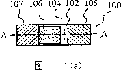
Fig. 1 is a light-emitting component of the present invention, and Fig. 1 (a) is an approximate vertical view, and Fig. 1 (b) is a summary section.
Fig. 2 is that light-emitting component is configured in approximate vertical view on the wafer in the light-emitting component of the present invention manufacturing process.
Fig. 3 is the key diagram of light-emitting element electrode configuration in the experiment of comparison luminous efficiency.
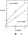
Fig. 4 is the luminous intensity diagrammatic sketch that is shown in each light-emitting component of Fig. 3.
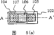
Fig. 5 is another light-emitting component of the present invention, and Fig. 5 (a) is its approximate vertical view, and Fig. 5 (b) is its summary section.
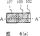
Fig. 6 is another light-emitting component of the present invention, and Fig. 6 (a) is its approximate vertical view, and Fig. 6 (b) is its summary section.
Fig. 7 is a light-emitting component in the past, and Fig. 7 (a) is its approximate vertical view, and Fig. 7 (b) is the summary section of Fig. 7 (a) along A-A ' line.
The working of an invention form
Light-emitting component of the present invention mainly is made of the 1st conductive type semiconductor layer that forms on substrate, the 2nd conductive type semiconductor layer, the 1st welding electrode, the 2nd welding electrode; Or constitute by the 1st conductive type semiconductor layer that on substrate, forms, the 2nd conductive type semiconductor layer, the 1st welding electrode, the 2nd electrode.There is no particular limitation for substrate, can be common light-emitting component as substrate use the sort of, but need to the light-emitting component that will obtain send only transparent, that is,, enough little for transparent near the absorption of the light of the wavelength emission light.For example, can be from semiconductor chips such as silicon, germanium, compound semiconductor substrates such as SiGe, SiC, GaP, GaAsP, GaN in the dielectric substrates such as sapphire, quartz, ZnO etc., are selected according to emission wavelength respectively.
Semiconductor layer in the light-emitting component of the present invention is made of at least 1 layer of the 1st conductive type semiconductor layer and the 2nd conductive type semiconductor layer, to form at least 1 pn knot.Here, so-called the 1st conduction type and the 2nd conduction type are represented any in p, n or the i type.
These semiconductor layers can be made of the semiconductor of same composition, also can be made of the semiconductor that difference is formed.These semiconductor layers between itself and substrate, between the semiconductor layer, between semiconductor layer and the 1st welding electrode or the 2nd electrode, can get involved the 1st, the 2nd conduction type or with the intermediate layer or the resilient coating of these 2 kinds of conduction type different conduction-types.
As semiconductor, be example with III family element nitride semiconductor, that is, gallium nitride based semiconductor for example removes In
sAl
tGa
1-s-tOutside the N (0≤s, 0≤t, s+t≤1) etc., can enumerate Al
sGa
1-sAs (0≤s≤1), Ga
sAs
1-sP (0≤s≤1), In
sGa
1-sAs
xP
1-x(0≤s≤1,0≤x≤1), In
sAl
tGa
1-s-tP (0≤s, 0≤t, s+t≤1), In
sAl
tGa
1-s-tN
xAs
1-x(0≤s, 0≤t, s+t≤1,0≤x≤1), In
sAl
tGa
1-s-tN
xP
1-x(0≤s, 0≤t, s+t≤1,0≤x≤1), Mg
sZn
tCd
1-s-tSxSe
yTe
1-x-y(0≤s, 0≤t, s+t≤1,0≤x, 0≤y, x+y≤1) etc., wherein, preferably gallium nitride based semiconductor, especially In
sAl
tGa
1-s-tN (0≤s, 0≤t, s+t≤1).
These semiconductor layers can contain concentration and be about 1 * 10
14~1 * 10
21Cm
-3N type or p type impurity, for example, C, Si, Ge, Sn, Be, Zn, Cd, Hg, Mg, O, S, Se, Te etc. also can be free from foreign meter.
Semiconductor layer can be by known method, for example formation such as MOCVD (mocvd) (metallo-organic compound vapour deposition) method, MBE (molecular beam epitaxy) method, MOMBE method, GSMBE (gas source molecular beam epitaxy) method.Again, impurity can mix when semiconductor layer forms, also can inject and the thermal diffusion method doping by ion after semiconductor layer forms.
The 1st conductive type semiconductor layer exposes the zone that is connected with the 1st welding electrode described later, preferably removes this regional superficial layer.As long as it is just passable that at this moment the size of the 1st welding electrode join domain has the required area of welding, for example, about 50~300 * 50~300 μ m
2, or constitute 1 light-emitting component the whole area of the 1st conductive type semiconductor layer about 5~50%.The thickness of the superficial layer of removing is about 0.5 ~ 10 μ m, or the whole thickness of the 1st conductive type semiconductor layer about 10~70%.
As the method for removing the 1st conductive type semiconductor layer part surface, available known method.Specifically, for example can enumerate use only has the wet corrosion method of mask and the acid solution or the alkaline solution of opening in this removal part, or uses the RIE method (reactive ion-etching) of all gases.For example, in the III group-III nitride semiconductor, using the RIE method that contains the halogen family elemental gas is effectively, specifically, can use Cl
2Gas and SiCl
4Gas.
The 2nd conductive type semiconductor layer can only be formed on the subregion of the 1st conductive type semiconductor layer.Its big I is suitably adjusted according to the luminous intensity that finally will obtain light-emitting component, and for example about 30~90% of the 1st conductive type semiconductor layer entire area.
Again, the 2nd conductive type semiconductor layer can use the method same with forming the 1st conduction type to form.In the time will being processed into intended shape, can by with as mentioned above, remove the identical method of the 1st conductive type semiconductor layer part surface and realize.
These semiconductor layers are because of common led chip profile is a rectangle, so best each self-forming rectangular shape.Here so-called " rectangular shape ", except that rectangle, also comprise square, trapezoidal, parallelogram, and then comprise that also its part or all of angle has circular shape, be semicircular shape, approximate semielliptical shape, if can be in led chip these semiconductor layers be provided with wasting space not.
The 1st welding electrode of light-emitting component of the present invention is the electrode that forms on the 1st conductive type semiconductor layer, can be formed by common conductive material.For example Al, In, Ga, Ni, Ti, Cu, Au, Ag, Cr, Si, W, WN, Pt, Pd, Ta, Sr etc.These materials can form the stacked film of monofilm or Ti/Au, W/Au etc.At this moment thickness concrete regulation not, more than for example about 0.5 μ m, best 1 μ m is above, below the 10 μ m.As long as it is just passable that its size has the required area of welding, as mentioned above, for example about 50~300 * 50~300 μ m
2Again, its shape does not have concrete regulation, preferably rectangle.
The formation method of the 1st welding electrode can consider that the material that uses suitably selects, and for example can use vacuum evaporating method, vacuum vapour deposition, EB vapour deposition method, ion plating method, MBE method, galvanoplastic, stencil printing etc.
The 1st welding electrode is usually formed for and the outside lead that is electrically connected.For the 1st welding electrode and conduction are connected firmly, also can form spherical portion.These leads and spherical portion can be used common used material.
The 2nd electrode of light-emitting component of the present invention is the electrode that almost forms on all surfaces at the 2nd conductive type semiconductor layer.
For example, (1) when the 2nd electrode forms when only being used for welding with the 2nd conductive type semiconductor layer, available and above-mentioned same material, thickness, method are formed.At this moment the size of the 2nd electrode is preferably formed as to welding required minimum in fact area, for example is about 50~300 * 50~300 μ m
2, preferably about 100~200 * 100~200 μ m
2, or be about 20~90% of the 1st conductive type semiconductor layer entire area that constitutes a light-emitting component.At this moment the 2nd electrode is preferably formed as to rectangle or is roughly rectangle.Its thickness for example is 0.5~10 μ m.Again, be preferably formed as to making 3 directions in the 2nd electrode perimeter, promptly with near the opposite side of a side of the 1st welding electrode, with this 3 side of 2 sides of this side adjacency under or under this 3 side near dispose light-emitting component the side.
(2) form at the 2nd electrode and be used for the 2nd conductive type semiconductor layer welding and during to its injection current, the 2nd electrode is made of the 2nd welding electrode and the 2nd transparency electrode.At this moment the 2nd welding electrode can be used with above-mentioned same material, thickness, method and form.At this moment the 2nd electrode size and the situation of above-mentioned (1) are same, be preferably formed as to welding required minimum in fact area, for example be about 50~300 * 50~300 μ m2, or constitute the 1st conductive type semiconductor layer entire area about 5~60% of a light-emitting component, or all areas of the 2nd conductive type semiconductor layer about 10~90%.The 2nd welding electrode is preferably formed as and is rectangle or approximate rectangular shape.Again, be preferably formed as and be 3 directions around the 2nd welding electrode, that is, with near the opposite side of the 1st welding electrode side, with this 3 side of 2 sides of this opposite side adjacency under or under this 3 side near the side of configuration light-emitting component.
The 2nd transparency electrode is electrically connected with the 2nd welding electrode, can be on the almost whole faces that are formed on the 2nd conductive type semiconductor layer under the 2nd welding electrode, also can form except that guaranteeing with the 2nd welding electrode bottom line is connected, not overlapping with the 2nd welding electrode.
The electrode material of the light that the 2nd transparency electrode usefulness can efficiently derive light-emitting component to be sent forms.For example, this radiative light transmittance is preferably about 30~100%.As electrode material, can enumerate metals such as Al, Au, Ni, Pd, Ti, Cr, Ta, Pt, Sr, SnO
2, transparent conductive materials such as ZnO, ITO are example.These materials can form monofilm or stacked film.Its thickness can suitably be adjusted so that suitable light transmission is arranged when stating material in the use, for example for below about 20nm, is preferably below about 15nm.On the other hand, even for making transverse current on semiconductor layer surface, must the lateral resistance of optically transparent electrode own compare with the resistance of semiconductor layer enough little, thereby more than the preferably about 2nm of its thickness.Particularly, when stack membranes such as use Ni/Au, Pd/Pt, thickness is preferably the scope of about 1~10nm/1~10nm.And when using the Pt monofilm, be about 2-20nm, be preferably about 2~10nm scope.
The formation method of the 2nd transparency electrode can suitably be selected according to the material that uses, and for example can use vacuum evaporating method, vacuum vapour deposition, EB vapour deposition method, ion plating method, MBE method etc.
At this moment, for example in one plane observe, then roughly foursquare the 1st welding electrode, the 2nd transparency electrode and the 2nd welding electrode are in line.
In the manufacture method of above-mentioned light-emitting component, preferably each light-emitting component is not single formation, but a plurality of light-emitting component forms in batch.That is, vertical and horizontal form the 1st conductive type semiconductor layer of one deck at least of a plurality of light-emitting components of a plurality of formations, one deck the 2nd conductive type semiconductor layer, the 1st welding electrode and the 2nd electrode at least on substrate.Then, the substrate that obtains is divided into the light-emitting component of a unit, a unit, also can be one group as required and cuts apart by 2 light-emitting components more than the unit.At this moment, preferably dispose each semiconductor layer and each electrode, make vertically, the 1st welding electrode and the 2nd electrode are adjacent to each other separately, laterally, and the 1st welding electrode and the 2nd electrode adjacency.Again, when the 2nd electrode is made of the 2nd welding electrode and the 2nd transparency electrode, preferably be configured to, laterally, the 1st welding electrode and the 2nd welding electrode adjacency.
Also can form in vertical the 1st welding electrode and the 2nd electrode 1 each and every one adjacency respectively, also can a plurality of the 1st welding electrodes or a plurality of the 2nd electrode form with being integrated.
A plurality of as mentioned above light-emitting components that form with being integrated, available known method, for example, scarification, die sinking method, laser intercept method etc. are cut apart.
In scarification, substrate thickness is adjusted to about 50~200 μ m, rules on wafer with the diamond scriber then, along the line ditch wafer is divided into chip.In the die sinking method, substrate thickness is adjusted into about 100~500 μ m, then, cut off wafer to be divided into chip with the rotating knife that solidifies diamond abrasive grain.In the laser intercept method, can use CO
2Laser, excimer laser or YLF Lasers, in order to cut off sapphire substrate, also wavelength available is the KrF excimer laser of 248nm.
Below, with reference to accompanying drawing, light-emitting component of the present invention and manufacture method thereof being described, the present invention is not limited to these embodiment.
The blue light emitting element of present embodiment is shown in Fig. 1 (a) and (b).This light-emitting component 100 is absorbing visible light hardly, the emission wavelength of this light-emitting component on the transparent sapphire substrate 101, is being formed n type GaN layer 102, InGaN luminescent layer 103, p type GaN layer 104 in turn.N type GaN layer 102 in its subregion, is removed part surface together with the InGaN luminescent layer 103 and the p type GaN layer 104 that form thereon, directly connects n type welding electrode 105 on this zone.On the subregion of p type transparency electrode 106, connect p type welding electrode 107 again.On n type welding electrode 105 and p type welding electrode 107, be connected spherical portion 108 and welding lead 109.
This light-emitting component 100 is configured to n type welding electrode 105, p type transparency electrode 106 and p type welding electrode 107 and is in line.In Fig. 1 (a),, spherical portion 108 and welding lead 109 have been omitted for being easy to observe.
The following describes the manufacture method of above-mentioned light-emitting component.
At first, be on the sapphire substrate 101 of 300 μ m at thickness, stacked above one another n type GaN layer 102, InGaN luminescent layer 103, p type GaN layer 104.
Then, adopt photoetching technique and dry etch techniques to remove this part surface that in the aftermentioned operation, will form p type GaN layer 104, InGaN luminescent layer 103 and n type GaN layer 102 in n type welding electrode 105 zones.
Then, on p type GaN layer 104, form the p type transparency electrode 106 that thickness is about the Ni/Au film formation of 15nm.At this moment the size of p type transparency electrode 106 is done into about 150 * 350 μ m
2On n type GaN layer 102, form the n type welding electrode 105 of the Al film formation of the about 1 μ m of thickness again.
And then, the p type welding electrode 107 that the Au film of the about 1 μ m of formation thickness constitutes on p type transparency electrode 106.Owing to be difficult to lead is welded on the p type transparency electrode 106 of metal film as thin as a wafer, this p type welding electrode is special the setting.The size of this p type welding electrode 107 need be made and consider to derive the required bottom line size of emission light, is the square of the length of side 200 μ m.
This operation usually as shown in Figure 2, a plurality of light-emitting components carry out in batch.That is, each welding electrode 105,107 forms a plurality of respectively with the state that connects together, and then light-emitting component 100 is cut apart as a unit and is made.
Before being divided into each light-emitting component 100, on substrate, check the characteristic of light-emitting component 100.This operation is to check when probe to contact p type welding electrode 107 and n type welding electrode 105 so that suitable electric current to be provided, element voltage that whether can obtain expecting and luminous intensity characteristic.In the present embodiment, as shown in Figure 2, be formed into light-emitting component 100 per 4 unit and connect welding electrode 105,107.Thereby, can concentrate inspection in per 4 unit.
According to configuration shown in Figure 2, want each welding electrode 105,107 of contact probe to form a line continuously, thereby in checking operation, probe only moves and can check along welding electrode 105,107, can not accidentally injure for example p type transparency electrode 106, can not fall dust etc. to transparency electrode 106 yet, can improve fabrication yield from probe.
Again, vertical at Fig. 2, do not require the tightness that the mask that is used to constitute each electrode 105,106,107 of light-emitting component etc. cooperates, thereby can simplify manufacturing process.
In operation thereafter, cut apart each light-emitting component that is shown in Fig. 2.Divided each element clamps to lift with collet chuck (vacuum suction instrument) does suitably carrying, at this moment, if adopt this collet chuck that only contacts with element two end portions (forming the side of p type welding electrode 107, n type welding electrode 105), then fix because of the element two ends, can stably carry, because of only having welding electrode, also can not injure the light guide of element again at the element two ends.This is by n type welding electrode, p type transparency electrode, p type welding electrode being configured to delegation in turn, only disposing the distinctive effect of light-emitting component of the present invention of welding electrode at the element two ends.
Then, on the not shown suitable pedestal of Fig. 1, fix each element, to n type welding electrode 105 and p type welding electrode 107 welding leads 109.At this moment, in the front end formation spherical portion 108 of welding lead 109, thus, firmly welding is finished.
In above-mentioned light-emitting component 100, shown in Fig. 1 (a), around the foursquare p type welding electrode 107 in 4 directions 3 directions become the side of light-emitting component 100.That is, in 3 directions, exposure luminescent layer 103 reaches the side to the substrate 101 of the optical transparency that is sent.Thereby, can outwards derive the light of being launched under the p type welding electrode 107 that can not fully derive in the light-emitting component in the past effectively.
The influence of each electrode configuration of light-emitting component to luminous efficiency experimentized.
As shown in Figure 3, make the illuminating part area do that various variations form as above-mentioned embodiment described around p type welding electrode 107 3 directions have the element side light-emitting component and as the prior art example be shown in p type welding electrode on every side 2 directions have the light-emitting component of element side, when injection has the electric current of same current density, compare the difference of luminous intensity.
The left-hand line of Fig. 3 is the light-emitting component that 3 directions have the element side around the p type welding electrode, and it is 1 that p type welding electrode area is established in expression, and illuminating part area (p type welding electrode and p type transparency electrode area sum) is the element of 3 kinds of situations of 1,2,3 o'clock.For example, represent among the figure: the illuminating part area is that 1 element is the element that does not form transparency electrode, and the illuminating part area is that 2 element is to form and the element of p type welding electrode with the transparency electrode of area.Again, right-hand column is the light-emitting component that 2 directions have the element side around the p type welding electrode.The illuminating part area, same as described above.In experiment, the size of p type welding electrode is the square of the every length of side 200 μ m, and the fixed thickness of sapphire substrate is 300 μ m.Per 1 area injects the 10mA electric current.
Experimental result is shown in Fig. 4.Fig. 4 relatively illustrates the luminous intensity of each light-emitting component that is shown in Fig. 3.
Among Fig. 4 result, arbitrary illuminating part area has equal big than the light-emitting component that has the element side in 2 directions of luminous intensity of the light-emitting component of element side in 3 directions.
By this result as can be known, even p type transparency electrode is provided with in abutting connection with p type welding electrode, also be difficult to derive the light that sends under the p type welding electrode, in order to improve leaded light, preferred plan is on every side as the element side with p type welding electrode.This effect, can not significantly embody launching in the only opaque light-emitting component at substrate.Its reason is, when using opaque substrate, substrate and on stacked semiconductor layer absorbed inside emission light, thereby the light of launching under the p type welding electrode almost can not directed outwards.But when using transparent substrate, if substrate side is in around the p type welding electrode, then the light of launching under the p type welding electrode can be derived by substrate side.
The result of Fig. 4 changes in substrate thickness is 60~400 mu m ranges hardly, at 100~200 * 100~200 μ m
2Suitable p type welding electrode magnitude range also almost constant.
Though p type welding electrode wishes that its area is little, guarantee to weld necessary area.The size of illuminating part also must suitably be provided with, in order to avoid injected current density is excessive.Its reason is, in case injected current density is excessive, because heating can reduce luminous efficiency, or component life is produced harmful effect.Therefore, form in the p type electrode that covers illuminating part, the minimum area that welding is required is as p type welding electrode, and remaining area is as p type transparency electrode, and is suitable to guarantee the illuminating part area.P type transparency electrode only is configured to the side in abutting connection with p type welding electrode, derives the light that sends under the p type welding electrode not hinder.
Like this, according to the light-emitting component of present embodiment 1, the area that makes p type welding electrode is required bottom line, with 3 directions as the element side, thereby can be effectively the photoconduction that sends under the p type welding electrode to element-external, compared with the prior art can improve the luminous efficiency of element.
In the present embodiment, I II family element nitride semiconductor is used for each semiconductor layer, thereby can obtains having the light-emitting component of good luminous characteristic in the visible light field again.
In Fig. 2,, promptly, then can obtain having the light-emitting component of 2 times of common light-emitting areas to cut light-emitting component shown in 110 like that as if being one group by per 2 light-emitting device unit.
Like this, the manufacture method according to the light-emitting component of present embodiment only changes part manufacturing process, can obtain having the light-emitting component of different light-emitting areas from a substrate.
The green luminescence element of present embodiment is shown in Fig. 5 (a) and 5 (b).This light-emitting component is formed on the inboard of leaving the about 30 μ m in element side except that p type welding electrode 107, and all the other are all identical in fact with embodiment 1.
In this embodiment, the thickness of sapphire substrate 101 is 100 μ m, and p type transparency electrode 106 is the rectangle of size 100 * 200 μ m, and p type welding electrode is the square of the length of side 100 μ m.
The light-emitting component of Gou Chenging can be derived the light that sends under the p type welding electrode 107 effectively from the element side also similarly to Example 1 like this.That is, can obtain luminous efficiency compared with the prior art good, at the luminous light-emitting component in visible light field.
The green-yellow light light-emitting component of present embodiment is shown in Fig. 6 (a) and reaches (b).This light-emitting component is except that omitting p type transparency electrode, and all the other are identical in fact with embodiment 1.
In the present embodiment, the thickness of sapphire substrate 101 is 200 μ m, and p type welding electrode 107 is the square of the length of side 150 μ m.
In the light-emitting component that so constitutes,, there is the problem of characteristic degradations such as luminous efficiency reduction under the high electric current because light-emitting area diminishes.Yet on the other hand, it is the LED element of purpose that this light-emitting component can be used for low output running with low current, thereby the simple and easy formation shown in Fig. 6 (a) and 6 (b) also can fully be used.
In this light-emitting component, the light of emission also can effectively be derived from the element side under the p type welding electrode 107, thereby can obtain having the light-emitting component of enough good characteristic, is the light-emitting component of purpose with low output running especially.
According to light-emitting component of the present invention, can derive in the past the light that does not effectively utilize, launch under the 2nd electrode from the element side to greatest extent, go out efficient thereby can improve the emission photoconduction.
By each semiconductor layer and electrode, can easyly easily make light-emitting component with suitable shape configuration light-emitting component of the present invention again.
Claims (5)
1. light-emitting component, it comprises:
Substrate,
At least 1 layer of the 1st conductive type semiconductor layer that on described substrate, forms,
At least 1 layer of the 2nd conductive type semiconductor layer that in the subregion of described the 1st conductive type semiconductor layer, forms,
Be connected to the 1st welding electrode of described the 1st conductive type semiconductor layer,
Be connected to the 2nd welding electrode on the whole surface of described the 2nd conductive type semiconductor layer; It is characterized in that,
Described substrate is only transparent to what launch near described the 1st conductive type semiconductor layer and the 2nd conductive type semiconductor layer junction surface;
Described the 2nd welding electrode forms the essentially rectangular shape and has the required minimum area in fact of welding;
The element side is configured in described the 2nd welding electrode 3 directions on every side.
2. light-emitting component, it comprises:
Substrate,
At least 1 layer of the 1st conductive type semiconductor layer that on substrate, forms,
At least 1 layer of the 2nd conductive type semiconductor layer that in the subregion of described the 1st conductive type semiconductor layer, forms,
Be connected to the 1st welding electrode of described the 1st conductive type semiconductor layer,
Be connected to almost the 2nd electrode on whole surface of described the 2nd conductive type semiconductor layer; It is characterized in that,
Described substrate is only transparent to what launch near described the 1st conductive type semiconductor layer and the 2nd conductive type semiconductor layer junction surface;
Described the 2nd electrode is made of the 2nd welding electrode and the 2nd transparency electrode;
Described the 2nd welding electrode forms the essentially rectangular shape and has the required minimum area in fact of welding;
The element side is configured in described the 2nd welding electrode 3 directions on every side;
Described light-emitting component top view has the quadrangle profile, and described the 1st welding electrode, the 2nd transparency electrode and the 2nd welding electrode are along the direction of this quadrangle one side linear array in regular turn.
3. light-emitting component as claimed in claim 1 or 2 is characterized in that, described the 1st conductive type semiconductor layer and the 2nd conductive type semiconductor layer are made of III family element nitride semiconductor.
4. a light-emitting component is a kind of LED with rectangular profile, and this light-emitting component comprises:
Substrate,
At least 1 layer of the 1st conductive type semiconductor layer that on substrate, forms,
At least 1 layer of the 2nd conductive type semiconductor layer that in the subregion of described the 1st conductive type semiconductor layer, forms,
Be connected to the 1st welding electrode of described the 1st conductive type semiconductor layer,
Be connected to almost the 2nd welding electrode on whole surface of described the 2nd conductive type semiconductor layer; It is characterized in that,
Described substrate is only transparent to what launch near described the 1st conductive type semiconductor layer and the 2nd conductive type semiconductor layer junction surface;
Described the 2nd welding electrode forms has the required minimum area in fact of welding;
Described the 2nd welding electrode is arranged to 3 sides in abutting connection with the LED profile;
Described light-emitting component top view has the quadrangle profile, and the described the 1st and the 2nd welding electrode is along the direction of this quadrangle one side linear array in regular turn;
The the described the 1st and the 2nd welding electrode area is 50 to 300 μ m
2Described substrate thickness is 60 to 400 μ m; Described the 2nd welding electrode is formed on the inboard apart from 3 about 30 μ m in side of rectangle light-emitting component.
5. a light-emitting component is a kind of LED with rectangular profile, and this light-emitting component comprises:
Substrate,
At least 1 layer of the 1st conductive type semiconductor layer that on substrate, forms,
At least 1 layer of the 2nd conductive type semiconductor layer that in the subregion of described the 1st conductive type semiconductor layer, forms,
Be connected to the 1st welding electrode of described the 1st conductive type semiconductor layer,
Be connected to almost the 2nd electrode on whole surface of described the 2nd conductive type semiconductor layer; It is characterized in that,
Described substrate is only transparent to what launch near described the 1st conductive type semiconductor layer and the 2nd conductive type semiconductor layer junction surface;
Described the 2nd electrode is made of the 2nd welding electrode and the 2nd transparency electrode;
Described the 2nd welding electrode forms has the required minimum area in fact of welding;
Described the 2nd welding electrode is arranged to 3 sides in abutting connection with the LED profile;
Described light-emitting component top view has the quadrangle profile, and described the 1st welding electrode, the 2nd transparency electrode and the 2nd welding electrode are along the direction of this quadrangle one side linear array in regular turn.
Applications Claiming Priority (3)
| Application Number | Priority Date | Filing Date | Title |
|---|---|---|---|
| JP79300/97 | 1997-03-31 | ||
| JP79300/1997 | 1997-03-31 | ||
| JP07930097A JP4203132B2 (en) | 1997-03-31 | 1997-03-31 | Light emitting device and manufacturing method thereof |
Publications (2)
| Publication Number | Publication Date |
|---|---|
| CN1251688A CN1251688A (en) | 2000-04-26 |
| CN100346487C true CN100346487C (en) | 2007-10-31 |
Family
ID=13686004
Family Applications (1)
| Application Number | Title | Priority Date | Filing Date |
|---|---|---|---|
| CNB988037610A Expired - Lifetime CN100346487C (en) | 1997-03-31 | 1998-03-25 | Light element device and method for manufacturing same |
Country Status (6)
| Country | Link |
|---|---|
| US (1) | US6583442B2 (en) |
| JP (1) | JP4203132B2 (en) |
| KR (1) | KR20010005846A (en) |
| CN (1) | CN100346487C (en) |
| TW (1) | TW392194B (en) |
| WO (1) | WO1998044569A1 (en) |
Families Citing this family (28)
| Publication number | Priority date | Publication date | Assignee | Title |
|---|---|---|---|---|
| US6413839B1 (en) * | 1998-10-23 | 2002-07-02 | Emcore Corporation | Semiconductor device separation using a patterned laser projection |
| JP3285341B2 (en) | 2000-06-01 | 2002-05-27 | 士郎 酒井 | Method of manufacturing gallium nitride based compound semiconductor |
| JP3466144B2 (en) | 2000-09-22 | 2003-11-10 | 士郎 酒井 | How to roughen the surface of a semiconductor |
| JP2002164570A (en) * | 2000-11-24 | 2002-06-07 | Shiro Sakai | Gallium nitride compound semiconductor device |
| JP3548735B2 (en) | 2001-06-29 | 2004-07-28 | 士郎 酒井 | Method of manufacturing gallium nitride based compound semiconductor |
| JP2003110139A (en) * | 2001-09-28 | 2003-04-11 | Sanyo Electric Co Ltd | Nitride semiconductor light emitting element |
| US20030132433A1 (en) * | 2002-01-15 | 2003-07-17 | Piner Edwin L. | Semiconductor structures including a gallium nitride material component and a silicon germanium component |
| TW543169B (en) * | 2002-02-08 | 2003-07-21 | Ritdisplay Corp | Package structure and process of organic light-emitting diode panel |
| US7005685B2 (en) | 2002-02-28 | 2006-02-28 | Shiro Sakai | Gallium-nitride-based compound semiconductor device |
| KR100497127B1 (en) * | 2002-09-05 | 2005-06-28 | 삼성전기주식회사 | AlGaInN semiconductor LED device |
| KR100543696B1 (en) * | 2002-09-09 | 2006-01-20 | 삼성전기주식회사 | Light emitting diode with high efficiency |
| JP4635985B2 (en) * | 2002-10-03 | 2011-02-23 | 日亜化学工業株式会社 | Light emitting diode |
| TW569409B (en) * | 2002-10-22 | 2004-01-01 | Ritek Display Technology Corp | Process for packaging an OLED panel |
| WO2004047189A1 (en) * | 2002-11-16 | 2004-06-03 | Lg Innotek Co.,Ltd | Light emitting device and fabrication method thereof |
| US20050051781A1 (en) * | 2003-09-08 | 2005-03-10 | United Epitaxy Company, Ltd. | Light emitting diode and method of making the same |
| JP2005259891A (en) * | 2004-03-10 | 2005-09-22 | Toyoda Gosei Co Ltd | Light emitting device |
| JP2008544540A (en) | 2005-06-22 | 2008-12-04 | ソウル オプト デバイス カンパニー リミテッド | Light emitting device and manufacturing method thereof |
| KR100661614B1 (en) | 2005-10-07 | 2006-12-26 | 삼성전기주식회사 | Nitride semiconductor light emitting device and method of manufacturing the same |
| JP5326225B2 (en) * | 2006-05-29 | 2013-10-30 | 日亜化学工業株式会社 | Nitride semiconductor light emitting device |
| JP5250856B2 (en) | 2006-06-13 | 2013-07-31 | 豊田合成株式会社 | Method for manufacturing gallium nitride compound semiconductor light emitting device |
| JP2010512662A (en) | 2006-12-11 | 2010-04-22 | ザ リージェンツ オブ ザ ユニバーシティ オブ カリフォルニア | Transparent light emitting diode |
| JP5235878B2 (en) * | 2007-06-15 | 2013-07-10 | ローム株式会社 | Semiconductor light emitting device |
| KR20100059820A (en) | 2007-07-26 | 2010-06-04 | 더 리전츠 오브 더 유니버시티 오브 캘리포니아 | Light emitting diodes with a p-type surface |
| JPWO2011111642A1 (en) * | 2010-03-08 | 2013-06-27 | 日亜化学工業株式会社 | Semiconductor light emitting device and manufacturing method thereof |
| US8785952B2 (en) * | 2011-10-10 | 2014-07-22 | Lg Innotek Co., Ltd. | Light emitting device and light emitting device package including the same |
| KR102546307B1 (en) * | 2015-12-02 | 2023-06-21 | 삼성전자주식회사 | Light emitting device and display device including the same |
| WO2018164371A1 (en) * | 2017-03-08 | 2018-09-13 | 엘지이노텍 주식회사 | Semiconductor device and semiconductor device package |
| CN108039126B (en) * | 2017-12-07 | 2021-04-23 | 大连海事大学 | LED array wiring method and display screen system |
Citations (4)
| Publication number | Priority date | Publication date | Assignee | Title |
|---|---|---|---|---|
| JPH07288340A (en) * | 1994-04-19 | 1995-10-31 | Mitsubishi Cable Ind Ltd | Light emitting element and manufacture thereof |
| JPH08102550A (en) * | 1994-09-30 | 1996-04-16 | Rohm Co Ltd | Semiconductor light emitting element |
| JPH08250769A (en) * | 1995-03-13 | 1996-09-27 | Toyoda Gosei Co Ltd | Optical semiconductor element |
| JPH0964418A (en) * | 1995-08-22 | 1997-03-07 | Fujitsu Ltd | Light emitting element and manufacture thereof |
Family Cites Families (6)
| Publication number | Priority date | Publication date | Assignee | Title |
|---|---|---|---|---|
| DE69433926T2 (en) * | 1993-04-28 | 2005-07-21 | Nichia Corp., Anan | A semiconductor device of a gallium nitride III-V semiconductor compound |
| JPH07254732A (en) * | 1994-03-15 | 1995-10-03 | Toshiba Corp | Semiconductor light emitting device |
| JP3121617B2 (en) * | 1994-07-21 | 2001-01-09 | 松下電器産業株式会社 | Semiconductor light emitting device and method of manufacturing the same |
| WO1997012405A1 (en) * | 1995-09-25 | 1997-04-03 | Nippon Sheet Glass Co., Ltd. | Surface light-emitting element and self-scanning type light-emitting device |
| JPH0964477A (en) * | 1995-08-25 | 1997-03-07 | Toshiba Corp | Semiconductor light emitting element and its manufacture |
| US6107644A (en) * | 1997-01-24 | 2000-08-22 | Rohm Co., Ltd. | Semiconductor light emitting device |
-
1997
- 1997-03-31 JP JP07930097A patent/JP4203132B2/en not_active Expired - Lifetime
-
1998
- 1998-03-24 TW TW087104416A patent/TW392194B/en not_active IP Right Cessation
- 1998-03-25 CN CNB988037610A patent/CN100346487C/en not_active Expired - Lifetime
- 1998-03-25 KR KR1019997008920A patent/KR20010005846A/en active Search and Examination
- 1998-03-25 WO PCT/JP1998/001355 patent/WO1998044569A1/en not_active Application Discontinuation
- 1998-03-25 US US09/402,493 patent/US6583442B2/en not_active Expired - Lifetime
Patent Citations (4)
| Publication number | Priority date | Publication date | Assignee | Title |
|---|---|---|---|---|
| JPH07288340A (en) * | 1994-04-19 | 1995-10-31 | Mitsubishi Cable Ind Ltd | Light emitting element and manufacture thereof |
| JPH08102550A (en) * | 1994-09-30 | 1996-04-16 | Rohm Co Ltd | Semiconductor light emitting element |
| JPH08250769A (en) * | 1995-03-13 | 1996-09-27 | Toyoda Gosei Co Ltd | Optical semiconductor element |
| JPH0964418A (en) * | 1995-08-22 | 1997-03-07 | Fujitsu Ltd | Light emitting element and manufacture thereof |
Also Published As
| Publication number | Publication date |
|---|---|
| US6583442B2 (en) | 2003-06-24 |
| KR20010005846A (en) | 2001-01-15 |
| JP4203132B2 (en) | 2008-12-24 |
| TW392194B (en) | 2000-06-01 |
| US20020121637A1 (en) | 2002-09-05 |
| JPH10275942A (en) | 1998-10-13 |
| WO1998044569A1 (en) | 1998-10-08 |
| CN1251688A (en) | 2000-04-26 |
Similar Documents
| Publication | Publication Date | Title |
|---|---|---|
| CN100346487C (en) | Light element device and method for manufacturing same | |
| US7183136B2 (en) | Semiconductor element and method for producing the same | |
| JP5556657B2 (en) | Group III nitride semiconductor light emitting device manufacturing method, group III nitride semiconductor light emitting device, and lamp | |
| US8716043B2 (en) | Method for manufacturing semiconductor light emitting diode | |
| KR101509834B1 (en) | Semiconductor light emitting element and method for manufacturing the same | |
| KR101077078B1 (en) | Gallium nitride compound semiconductor light emitting element | |
| KR100724540B1 (en) | Laser beam delivery system and method thereof, and laser lift-off method | |
| CN1471735A (en) | Method for producing a radiation-emitting semiconductor chip based on III-V nitride semiconductor material and a corresponding radiation-emitting semiconductor chip | |
| CN1178303C (en) | Semiconductor laminated substrate, crystal substrate and semiconductor device and manufacturing method thereof | |
| CN1943050A (en) | Production method of compound semiconductor light-emitting device wafer | |
| KR101035878B1 (en) | Group ? nitride semiconductor light-emitting device | |
| CN1858921A (en) | Flip chip light emitting diode and method of manufactureing the same | |
| CN1744337A (en) | Nitride-based compound semiconductor light emitting device | |
| CN1652364A (en) | Nitride-based light-emitting device and method of manufacturing the same | |
| WO2005091385A1 (en) | Semiconductor light-emitting device and illuminating device | |
| KR20150022771A (en) | Light emitting device comprising chip-on-board package substrate and method for manufacturing same | |
| CN1781195A (en) | Method for making group III nitride devices and devices produced thereby | |
| CN1476641A (en) | Semiconductor light-emitting device, image display, illuminator and its mfg. method | |
| CN1147010C (en) | Self-passinvating non-planar junction subgroup III nitride semi-conductor device and its making method | |
| JP2006253670A (en) | Nitride semiconductor light-emitting device and method of fabricating the same | |
| JP2004200639A (en) | Manufacturing method of light emitting diode element, and the light emitting diode element | |
| CN1893135A (en) | Vertical structure light emitting diode and fabricating method thereof | |
| KR102075994B1 (en) | Substrate separation device and substrate separation system | |
| JP2004228290A (en) | Semiconductor light emitting element and its fabricating process | |
| CN102244173A (en) | Light-emitting element and manufacturing method thereof |
Legal Events
| Date | Code | Title | Description |
|---|---|---|---|
| C06 | Publication | ||
| PB01 | Publication | ||
| C10 | Entry into substantive examination | ||
| SE01 | Entry into force of request for substantive examination | ||
| C14 | Grant of patent or utility model | ||
| GR01 | Patent grant | ||
| CX01 | Expiry of patent term |
Granted publication date: 20071031 |
|
| CX01 | Expiry of patent term |