CN100345254C - Formation of high-mobility silicon-germanium structures by low-energy plasma enhanced chemical vapor deposition - Google Patents
Formation of high-mobility silicon-germanium structures by low-energy plasma enhanced chemical vapor deposition Download PDFInfo
- Publication number
- CN100345254C CN100345254C CNB028273095A CN02827309A CN100345254C CN 100345254 C CN100345254 C CN 100345254C CN B028273095 A CNB028273095 A CN B028273095A CN 02827309 A CN02827309 A CN 02827309A CN 100345254 C CN100345254 C CN 100345254C
- Authority
- CN
- China
- Prior art keywords
- substrate
- layer
- growth room
- growing system
- growth
- Prior art date
- Legal status (The legal status is an assumption and is not a legal conclusion. Google has not performed a legal analysis and makes no representation as to the accuracy of the status listed.)
- Expired - Fee Related
Links
- 230000015572 biosynthetic process Effects 0.000 title claims description 3
- 238000000623 plasma-assisted chemical vapour deposition Methods 0.000 title abstract 3
- LEVVHYCKPQWKOP-UHFFFAOYSA-N [Si].[Ge] Chemical group [Si].[Ge] LEVVHYCKPQWKOP-UHFFFAOYSA-N 0.000 title description 4
- 238000000034 method Methods 0.000 claims abstract description 52
- 239000000758 substrate Substances 0.000 claims abstract description 43
- 239000007789 gas Substances 0.000 claims abstract description 35
- 229910052710 silicon Inorganic materials 0.000 claims abstract description 13
- XUIMIQQOPSSXEZ-UHFFFAOYSA-N Silicon Chemical compound [Si] XUIMIQQOPSSXEZ-UHFFFAOYSA-N 0.000 claims abstract description 12
- 239000004065 semiconductor Substances 0.000 claims abstract description 12
- 239000010703 silicon Substances 0.000 claims abstract description 11
- 239000001257 hydrogen Substances 0.000 claims abstract description 7
- 229910052739 hydrogen Inorganic materials 0.000 claims abstract description 7
- 239000011248 coating agent Substances 0.000 claims description 19
- 238000000576 coating method Methods 0.000 claims description 19
- 238000004519 manufacturing process Methods 0.000 claims description 10
- 230000003746 surface roughness Effects 0.000 claims description 10
- 239000012535 impurity Substances 0.000 claims description 8
- 239000000126 substance Substances 0.000 claims description 4
- UFHFLCQGNIYNRP-UHFFFAOYSA-N Hydrogen Chemical compound [H][H] UFHFLCQGNIYNRP-UHFFFAOYSA-N 0.000 claims description 3
- 239000004094 surface-active agent Substances 0.000 claims description 3
- 238000000151 deposition Methods 0.000 claims 3
- 239000007792 gaseous phase Substances 0.000 claims 3
- 125000004435 hydrogen atom Chemical class [H]* 0.000 abstract description 4
- 229910006990 Si1-xGex Inorganic materials 0.000 abstract 2
- 229910007020 Si1−xGex Inorganic materials 0.000 abstract 2
- 239000002019 doping agent Substances 0.000 abstract 1
- 239000010410 layer Substances 0.000 description 55
- 229910000577 Silicon-germanium Inorganic materials 0.000 description 42
- 238000005229 chemical vapour deposition Methods 0.000 description 25
- 239000011247 coating layer Substances 0.000 description 14
- 238000001451 molecular beam epitaxy Methods 0.000 description 10
- 238000000038 ultrahigh vacuum chemical vapour deposition Methods 0.000 description 10
- 230000000694 effects Effects 0.000 description 6
- 229910052732 germanium Inorganic materials 0.000 description 5
- 238000005516 engineering process Methods 0.000 description 4
- 238000004518 low pressure chemical vapour deposition Methods 0.000 description 4
- 125000004429 atom Chemical group 0.000 description 3
- 230000006835 compression Effects 0.000 description 3
- 238000007906 compression Methods 0.000 description 3
- 238000010586 diagram Methods 0.000 description 3
- GNPVGFCGXDBREM-UHFFFAOYSA-N germanium atom Chemical compound [Ge] GNPVGFCGXDBREM-UHFFFAOYSA-N 0.000 description 3
- 239000000463 material Substances 0.000 description 3
- 239000000203 mixture Substances 0.000 description 3
- 241000193935 Araneus diadematus Species 0.000 description 2
- XKRFYHLGVUSROY-UHFFFAOYSA-N Argon Chemical compound [Ar] XKRFYHLGVUSROY-UHFFFAOYSA-N 0.000 description 2
- 238000005336 cracking Methods 0.000 description 2
- 230000002950 deficient Effects 0.000 description 2
- 238000010891 electric arc Methods 0.000 description 2
- 230000035515 penetration Effects 0.000 description 2
- 238000005498 polishing Methods 0.000 description 2
- 229910008310 Si—Ge Inorganic materials 0.000 description 1
- 229910045601 alloy Inorganic materials 0.000 description 1
- 239000000956 alloy Substances 0.000 description 1
- 238000004458 analytical method Methods 0.000 description 1
- 229910052786 argon Inorganic materials 0.000 description 1
- 238000000429 assembly Methods 0.000 description 1
- 230000000712 assembly Effects 0.000 description 1
- 238000010923 batch production Methods 0.000 description 1
- 230000005540 biological transmission Effects 0.000 description 1
- 238000006243 chemical reaction Methods 0.000 description 1
- 239000012141 concentrate Substances 0.000 description 1
- 239000013078 crystal Substances 0.000 description 1
- 238000009792 diffusion process Methods 0.000 description 1
- 238000009826 distribution Methods 0.000 description 1
- 238000000407 epitaxy Methods 0.000 description 1
- 230000008020 evaporation Effects 0.000 description 1
- 238000001704 evaporation Methods 0.000 description 1
- 230000005669 field effect Effects 0.000 description 1
- 238000001534 heteroepitaxy Methods 0.000 description 1
- 238000002347 injection Methods 0.000 description 1
- 239000007924 injection Substances 0.000 description 1
- 238000003475 lamination Methods 0.000 description 1
- 238000004377 microelectronic Methods 0.000 description 1
- 238000006386 neutralization reaction Methods 0.000 description 1
- 239000011148 porous material Substances 0.000 description 1
- 239000002243 precursor Substances 0.000 description 1
- 238000001289 rapid thermal chemical vapour deposition Methods 0.000 description 1
- 230000000630 rising effect Effects 0.000 description 1
- 239000007787 solid Substances 0.000 description 1
- 230000008719 thickening Effects 0.000 description 1
- NFACJZMKEDPNKN-UHFFFAOYSA-N trichlorfon Chemical compound COP(=O)(OC)C(O)C(Cl)(Cl)Cl NFACJZMKEDPNKN-UHFFFAOYSA-N 0.000 description 1
- 230000005533 two-dimensional electron gas Effects 0.000 description 1
Images


Classifications
-
- H—ELECTRICITY
- H01—ELECTRIC ELEMENTS
- H01L—SEMICONDUCTOR DEVICES NOT COVERED BY CLASS H10
- H01L29/00—Semiconductor devices adapted for rectifying, amplifying, oscillating or switching, or capacitors or resistors with at least one potential-jump barrier or surface barrier, e.g. PN junction depletion layer or carrier concentration layer; Details of semiconductor bodies or of electrodes thereof ; Multistep manufacturing processes therefor
- H01L29/66—Types of semiconductor device ; Multistep manufacturing processes therefor
- H01L29/68—Types of semiconductor device ; Multistep manufacturing processes therefor controllable by only the electric current supplied, or only the electric potential applied, to an electrode which does not carry the current to be rectified, amplified or switched
- H01L29/76—Unipolar devices, e.g. field effect transistors
- H01L29/772—Field effect transistors
- H01L29/778—Field effect transistors with two-dimensional charge carrier gas channel, e.g. HEMT ; with two-dimensional charge-carrier layer formed at a heterojunction interface
- H01L29/7782—Field effect transistors with two-dimensional charge carrier gas channel, e.g. HEMT ; with two-dimensional charge-carrier layer formed at a heterojunction interface with confinement of carriers by at least two heterojunctions, e.g. DHHEMT, quantum well HEMT, DHMODFET
-
- H—ELECTRICITY
- H01—ELECTRIC ELEMENTS
- H01L—SEMICONDUCTOR DEVICES NOT COVERED BY CLASS H10
- H01L21/00—Processes or apparatus adapted for the manufacture or treatment of semiconductor or solid state devices or of parts thereof
- H01L21/02—Manufacture or treatment of semiconductor devices or of parts thereof
- H01L21/02104—Forming layers
- H01L21/02365—Forming inorganic semiconducting materials on a substrate
- H01L21/02367—Substrates
- H01L21/0237—Materials
- H01L21/02373—Group 14 semiconducting materials
- H01L21/02381—Silicon, silicon germanium, germanium
-
- H—ELECTRICITY
- H01—ELECTRIC ELEMENTS
- H01L—SEMICONDUCTOR DEVICES NOT COVERED BY CLASS H10
- H01L21/00—Processes or apparatus adapted for the manufacture or treatment of semiconductor or solid state devices or of parts thereof
- H01L21/02—Manufacture or treatment of semiconductor devices or of parts thereof
- H01L21/02104—Forming layers
- H01L21/02365—Forming inorganic semiconducting materials on a substrate
- H01L21/02436—Intermediate layers between substrates and deposited layers
- H01L21/02439—Materials
- H01L21/02441—Group 14 semiconducting materials
- H01L21/0245—Silicon, silicon germanium, germanium
-
- H—ELECTRICITY
- H01—ELECTRIC ELEMENTS
- H01L—SEMICONDUCTOR DEVICES NOT COVERED BY CLASS H10
- H01L21/00—Processes or apparatus adapted for the manufacture or treatment of semiconductor or solid state devices or of parts thereof
- H01L21/02—Manufacture or treatment of semiconductor devices or of parts thereof
- H01L21/02104—Forming layers
- H01L21/02365—Forming inorganic semiconducting materials on a substrate
- H01L21/02436—Intermediate layers between substrates and deposited layers
- H01L21/02494—Structure
- H01L21/02496—Layer structure
- H01L21/02502—Layer structure consisting of two layers
-
- H—ELECTRICITY
- H01—ELECTRIC ELEMENTS
- H01L—SEMICONDUCTOR DEVICES NOT COVERED BY CLASS H10
- H01L21/00—Processes or apparatus adapted for the manufacture or treatment of semiconductor or solid state devices or of parts thereof
- H01L21/02—Manufacture or treatment of semiconductor devices or of parts thereof
- H01L21/02104—Forming layers
- H01L21/02365—Forming inorganic semiconducting materials on a substrate
- H01L21/02436—Intermediate layers between substrates and deposited layers
- H01L21/02494—Structure
- H01L21/02496—Layer structure
- H01L21/0251—Graded layers
-
- H—ELECTRICITY
- H01—ELECTRIC ELEMENTS
- H01L—SEMICONDUCTOR DEVICES NOT COVERED BY CLASS H10
- H01L21/00—Processes or apparatus adapted for the manufacture or treatment of semiconductor or solid state devices or of parts thereof
- H01L21/02—Manufacture or treatment of semiconductor devices or of parts thereof
- H01L21/02104—Forming layers
- H01L21/02365—Forming inorganic semiconducting materials on a substrate
- H01L21/02518—Deposited layers
- H01L21/02521—Materials
- H01L21/02524—Group 14 semiconducting materials
- H01L21/02532—Silicon, silicon germanium, germanium
-
- H—ELECTRICITY
- H01—ELECTRIC ELEMENTS
- H01L—SEMICONDUCTOR DEVICES NOT COVERED BY CLASS H10
- H01L21/00—Processes or apparatus adapted for the manufacture or treatment of semiconductor or solid state devices or of parts thereof
- H01L21/02—Manufacture or treatment of semiconductor devices or of parts thereof
- H01L21/02104—Forming layers
- H01L21/02365—Forming inorganic semiconducting materials on a substrate
- H01L21/02612—Formation types
- H01L21/02617—Deposition types
- H01L21/0262—Reduction or decomposition of gaseous compounds, e.g. CVD
Abstract
Method for making semiconductor structures comprising the steps: forming a virtual substrate on a silicon substrate with a graded Si1-xGex layer and a non-graded Si1-xGex layer, using a high-density, low-energy plasma enhanced chemical vapor deposition (LEPECVD) process with a growth rate above 2nm/s, a substrate temperature between 400 DEG and 850 DEG C, and a total reactive gas flow at the gas inlet between 5 sccm and 200 sccm; forming an active region on the virtual substrate that comprises a Ge-channel and at least one modulation-doped layer using a low-density, low-energy plasma enhanced chemical vapor deposition (LEPECVD) process by introducing hydrogen (H2) into the growth chamber, maintaining a substrate temperature between 400 DEG and 500 DEG C, and by introducing a dopant gas in a pulsed manner into the growth chamber to provide for the modulation-doped layer.
Description
Technical field
The present invention relates to the formation of silicon germanium structure, more particularly, relate to the heterostructure that some anxious electronation hole mobility occurs.For example, adopt following method can form modulation-doped FET structure (for example, MODFET structure) and modulation doped quantum well structures (for example, MODQW structure).
Background technology
Some new material and material compositions are being adopted in industry at present, to improve such as transistorized semiconductor device.Can improve the processing speed and the performance of integrated circuit (ICs) like this.
One typical example is to dispose SiGe (SiGe) on silicon.Figure 1 shows that the example of a well-known SiGe heterostructure device 10.This device 10 comprises one (001) directed silicon chip 11.One graded SiGe layer 12 is positioned on the Si substrate 11.Layer 12 is to consider that lattice constant little by little changes over main by the determined lattice constant of Ge concentration in the SiGe layer 12 by the lattice constant of silicon.In the described example, the resilient coating 13 of a components unchanged forms on this classification SiGe layer 12.This SiGe layer 12 and the virtual substrate of resilient coating 13 as other layers that in operation subsequently, form.Form one group of active element layer 14 on this virtual substrate.The Figure 15 on the left side of described device 10 is described to be the concentration of Ge.Ge concentration (x) in the described SiGe layer 12 increases to x=x gradually by x=0
fThe thickness of described layer 12 generally is several microns, concentrates low to guarantee defective.
The existing manufacture method that the SiGe device 10 of several extensive employings is arranged, example is as, molecular beam epitaxy (MBE) and high vacuum chemical vapour deposition (UHV-CVD).It is then very difficult to adopt described method to make the SiGe structure and the device that are rich in Ge.Another shortcoming of known method is that growth rate is slow.Concentrating in an acceptable level in order to ensure defective, is a certain minimum value so require the thickness of SiGe layer 12.Like this, form described germanium-silicon layer and then need considerable time.Therefore, be very disadvantageous for a large amount of production of industrialness.
Two kinds of different UHV-CVD tool methods are arranged.First kind is called hot wall type UHV-CVD and second kind and is called cold wall type UHV-CVD or hot CVD (RTCVD) fast.
Hot wall type CVD is fit to batch process and carries out under low substrate temperature (generally between 450 ℃ and 550 ℃) very much.Adopt hot wall UHV-CVD can on the SiGe resilient coating, form strain Si ditch.People such as Ismail are report in being entitled as " in the Si/SiGe modulation-doped heterostructure high electron mobility " (Appl.Phys.Lett, Vol.66, p.1077,1995) once, and high electron mobility is greater than 10
5Cm
2/ Vs.Described hot wall type UHV-CVD has following shortcomings, for example:
-being entitled as report in " the common growth phenomenon of silicon/germanium low-temperature epitaxy " (Appl.Phys.Lett., Vol.53, p.2555,1988) according to people such as B.S.Meyerson, pure Si growth rate (approximately nm/minute) under about 550 ℃ substrate temperature is slow;
-by the roughness of so-called cross spider because of the lax big surface that causes.Concentration gradient (classification rate) is steep more, and the effect of described cross spider is then obvious more.The gap of height is about 30nm (nanometer) usually on the height, even have the dense (x that crosses of lower surperficial Ge one
fOn the surface of resilient coating=0.3).As people such as M.Arafa be entitled as " device of high-performance Si/SiGe field-effect transistor and manufacturing issue " (Mat.Sci.Soc., Symp.Proc.Vol.533, p.83) described in, surface roughness has disadvantageous effect to the quality of MODFETs.
-being entitled as described in " SiGe technology: heteroepitaxy and high speed microelectronics " (Annu.Rev.Mater.Sci., Vol.30, pp.335,2000) as people such as P.M.Mooney, the hot wall method is difficult to control especially when high Ge concentration.Therefore, described hot wall method is not suitable for the high-mobility hole transmission.Like this, adopt the hot wall technology can not obtain to have the high-performance p-MODFETs of pure Ge ditch.
Cold wall CVD is suitable as the processing single-chip.Described processing is being carried out more than 700 ℃ usually.Write people such as E.A.Fitzgerald and to be entitled as that " growth has the lax fully Ge of low penetration type dislocation density on the Si substrate
xSi
X-1Layer " in the paper of (Appl.Phys.Lett., Vol.59, p.811,1991), can find first result of relevant classification SiGe resilient coating.When substrate temperature between 800 ℃ and 900 ℃, surface roughness is bigger than the laminar surface roughness of making of the hot wall method.Report is pointed out, when the Ge of resilient coating concentration increases, at Si
0.7Ge
0.3The RMS-roughness of one 30 nanometers on the resilient coating will tend to bigger surface roughness.For further details, please refer to people's such as S.B.Samavedan article, be entitled as " novel dislocation structure and configuration of surface effect in lax Ge/Si-Ge (classification)/Si structure " (J.Appl.Phys, Vol.81, p.3108,1997).
When adopting cold wall UHV-CVD to make (the RMS roughness is greater than 30nm), the SiGe resilient coating is very coarse, and wherein concentration becomes gradient, so that obtain 100%Ge on the surface of resilient coating.As then can not on these rough surfaces, forming heterostructure device without chemico-mechanical polishing (CMP).Details please refer to people's such as E.A.Fitzgerald article, are entitled as " adopting gradual SiGe layer and chemico-mechanical polishing to control the penetration type dislocation density of the Ge on the Si " (Appl.Phys.Lett, Vol.72, p.1718,1998).
Until now, also adopt cold wall UHV-CVD to make the cavity conveying device of MODFET structure and high mobility without any the whole lamination of report.
Another well-known treatment technology is low-pressure chemical vapor deposition (LPCVD).Article as people such as A.C.Churchill, be entitled as " the high mobility two-dimensional electron gas in the Si/SiGe allosome structure under the high temperature on the lax SiGe layer of growth " (Semicond.Sci.Technol., Vol.12, p.943,1998) report in, the high processing temperature in the LPCVD method also can cause big surface roughness.Described situation also occurs in the classification rate and is lower than 10%/μ m.According to reports, when the Ge of buffer-layer surface concentration be x
f=0.24 and substrate temperature when being 800 ℃, the RMS roughness can be up to 6nm.Details please refer to people's such as D.J.Wallis article, are entitled as " the mosaic crystal gradient in the lax SiGe layer and with the relation of dislocation structure, surface roughness and growth conditions " (Mat.Res.Soc.Symp.Proc., 533, p.77,1998).
Lip-deep Ge concentration is 100% (to be x
f=1) classification resilient coating has bigger roughness, and promptly RMS is 160nm.
As cold wall UHV-CVD, LPCVD is not suitable for making a structure that needs high hole mobility.
As mentioned above, MBE is that another extensively adopts the method for making semiconductor structure.Adopt a MBE method can make a virtual substrate (layer 12 of Fig. 1 and layer 13), do not occur and do not have a serious difficult problem.Because the chemical composition of layer is irrelevant with substrate temperature basically, so,, be entitled as " the Si/Si of classification on the composition as people's such as J.-H.Li article by selecting suitable hygrogram and classification rate can optimize the lax and surface roughness of virtual substrate layer
1-xGe
xThe strain relaxation of resilient coating and surface morphology " described in people's such as (J.-Vac.Sci.Technol., Vol.B16, p.1610,1998) and E.A.Fitzgerald the article (APL, Vol.59, p.811,1991).
The important disadvantages of MBE is the finite capacity of evaporation crucible.This is unfavorable especially when making thick SiGe buffer growth, as people's such as T.Hackbarth article, is entitled as described in " alternative plan of the SiGe resilient coating that MBE growth thickening is lax " (Thin Solid Films, Vol.369, p.148,2000).Therefore, MBE is not suitable for the industrial-scale production of SiGe device.
For the device that has the compression strain ditch of a large amount of Ge on the virtual substrate, it tends to three dimensional growth.Specifically, pure Ge layer is except growth under about 300 ℃ low substrate temperature, and it presents obvious surface roughness.Yet, in the electrical properties that still can not accept at present the device under such low temperature.
The purpose of this invention is to provide a kind of manufacture method through improved SiGe structure, for example, MODFET structure or MODQW structure.
Another object of the present invention provides a kind of manufacture method with the SiGe device through improving hole conductivity.
A further object of the present invention provides the device through improved SiGe heterostructure.
Another purpose of the present invention provides a kind of growing system of manufacture method of the SiGe of enforcement device.
Summary of the invention
The present invention depends on a kind of low energy plasma and strengthens chemical vapour deposition (CVD) (LEPECVD) method.
The present invention proposes a kind of manufacture method of semiconductor structure, and its step comprises:
-adopting the high density low energy plasma to strengthen chemical vapour deposition (CVD) (LEPECVD) method: the speed of growth is 2nm/ more than second, and substrate temperature has a gross activity gas flow between 400 ℃ and 850 ℃ and in the gas access be 5sccm~200sccm (standard cm
3/ minute), with classification Si
1-xGe
xLayer and non-graded Si
1-xGe
xLayer forms a virtual substrate on a silicon chip.
In addition, the step of described method also comprises:
-adopt a low-density low energy plasma to strengthen the method for chemical vapour deposition (CVD) (LEPECVD): make hydrogen (H
2) entering the growth room, substrate temperature maintains between 400 ℃ and 500 ℃ and with pulse mode and makes an impurity gas enter the growth room, so that modulate-doped layer to be provided, to comprise on the virtual substrate of a Ge ditch and at least one modulate-doped layer one and to form an active region.
The present invention proposes a kind of semiconductor device.This device comprises a silicon chip, a classification Si
1-xGe
xLayer, one has the Si of constant Ge content
1-xGe
xResilient coating and one is positioned at described Si
1-xGe
xActive region on the resilient coating.This active region comprises at least one modulate-doped layer and and has 70000 and 87000cm at 4.2k
2The Ge ditch of/Vs hole mobility.
The present invention proposes a kind of growing system.This system comprises that one has the growth room of gas access.The setting of this system can be implemented a low energy plasma and strengthen chemical vapour deposition (CVD) (LEPECVD) method, and this method comprises at least two treatment steps, wherein:
-system parameters of first treatment step to be adjusted to: substrate temperature is 400 ℃~850 ℃, and place, gas access gross activity gas flow is 5sccm~200sccm, so that growth rate is more than the 2nm/s; And
-system parameters of second treatment step to be adjusted to: substrate temperature maintains 400 ℃~850 ℃, makes hydrogen (H
2) inject the growth room and adopt pulse mode to make impurity gas inject the growth room, so that one deck modulation doping at least.
The invention has the advantages that and to prevent or even avoid the obstacle and the shortcoming of known method.Described device can be realized unknown so far hole mobility.Described growth rate sharply increases, and therefore, method of the present invention be can be used in commercial scale make semiconductor device.Other advantages will be more obvious from following detailed description.
Description of drawings
Below, will more be described in detail the present invention, further purpose of the present invention and advantage in conjunction with the accompanying drawings, wherein:
Figure 1 shows that the schematic cross-section of SiGe heterostructure semiconductor device;
Figure 2 shows that low energy plasma of the present invention strengthens the schematic cross-section of chemical vapour deposition (CVD) (LEPECVD) system;
Figure 3 shows that the schematic diagram of Ge concentration changes with time of the present invention;
Figure 4 shows that the temperature variant schematic diagram of hole mobility of various sample of the present invention;
Figure 5 shows that the schematic cross-section of SiGe heterostructure semiconductor device of the present invention;
Figure 6 shows that the schematic cross-section of another SiGe heterostructure semiconductor device of the present invention;
Figure 7 shows that the schematic diagram of Ge concentration changes with time of the present invention; With
Figure 8 shows that the calcspar of growing system of the present invention.
Embodiment
Principle of the present invention is the layer extension of strain when utilizing the material of two kinds of different crystalline lattice parameters to grow mutually thereon.For example, when germanium (Ge) was deposited on the substrate of a less lattice parameter, the atom of Ge and the atom under it are in line so that Ge compression crustal strain.In the Ge of strain, for example, the hole runs into less resistance, will flow comparatively fast.This effect can be used for realizing device faster and need not reduce the size of individual devices.
Space between the silicon atom is littler than the lattice of germanium.Therefore, the lattice constant of a SiGe layer is bigger than the lattice constant of silicon.The SiGe lattice constant increases with the concentration rising of Ge.
The present invention relies on the low-power plasma body to strengthen chemical vapour deposition (CVD) (LEPECVD).Figure 2 shows that a typical LEPECVD system 20.LEPECVD is based on 22 li in a plasma chamber hot filament 21 and the wall of growth room 23 and/or the discharge of the low voltage DC electric arc between the auxiliary anode 24.The substrate 25 that one SiGe layer will form thereon is directly exposed to high strength but in the low-energy plasma.Voltage pact-the 12V (volt) of this substrate is such as the infringement that prevents any energetic ion.One substrate bias controller 31 applies a suitable bias voltage.Described LEPECVD is characterised in that plasma potential is near 0V.Necessary active gases (for example, H
2, SiH
4, GeH
4And PH
3) directly inject growth room 23 by a hole 26 and a gas access 30, simultaneously, argon (Ar) discharge gas then infeeds plasma chamber 22 by a hole 27, and this chamber is connected with growth room 23 and is separated by a pore 28.High-intensity plasma makes precursor gas (for example, SiH
4And GeH
4Deng) cracking very effectively, so that Si and SiGe film have extra high growth rate.In addition, growth rate is strengthened by plasma is limited in the magnetic field that is produced by the coil that is centered around growth room 23.Adopt an appropriate voltage to make the AC electric current by described filament 21.The electric current of about 120A makes filament 21 be heated to the temperature of requirement.In addition, the dc voltage power supply 32 with an about 25V produces an arc discharge between filament 21 and ground.This system 20 also comprises a turbomolecular pump 29.
The further details of LEPECVD system were described in such as PCT patent application WO 98/58099 already.The details of described PCT patent application are then as reference together.
The advantage of LEPECVD system is the plasma density that can obtain extra-high-speed.Virtual substrate of the present invention is to adopt highdensity plasma-grown.The cracking of described active gases is very effective to high-density plasma, so that increase growth power.Substrate temperature then has the high growth rate up to 10nm/s between 400 ℃ and 850 ℃.Except traditional CVD system, the temperature fully similar and substrate in specific temperature range of the growth rate in the LEPECVD system is irrelevant.
The present invention proved already, the SiGe growth rate in the LEPECVD system almost with the growth room in irrelevant with the concentration of the reacting gas of a fixing total flow.In traditional CVD system, has strong correlation between the concentration of growth rate and gas.
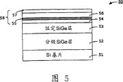
The present invention adopts a kind of method that is called modulation doping, realizes whereby mixing in a LEPECVD system as shown in Figure 2.The basic principle of described modulation doping is almost identical with other growing methods.Doped layer and hole delivery ditch does not directly contact, for example described in the paper of being delivered in Appl.Phys.Lett. (Vol.63, p.2263,1993) as people such as Xie.Be one how to realize the typical example that mixes described in Fig. 3, wherein the concentration of Ge is with the function representation of time (second).This figure itself has shown the Ge ditch Ge stream before growth, after the growth neutralization growth.10 Wei Shiyue are about 70 seconds the described doping of 10 diborane pulses, 41 realizations with each pulse connecting time.In these diborane pulses 41, make Ge stream reduce to zero.Figure 5 shows that the corresponding heterostructure device 50 of the present invention.This device comprises a Si substrate 51, forms a virtual SiGe substrate on it.This virtual substrate comprises the resilient coating 53 of a classification SiGe layer 52 and a Ge constant concentration.The thickness and the not to scale that please note different layers are drawn.One active region 58 is positioned on this virtual substrate.This active region comprises a coating layer 54, and the Ge concentration that the Ge concentration ratio layer of described layer is 53 li is low.Ge ditch 55 is arranged on the coating layer 54.An one modulation doping coating layer 56 and a Si cover layer 57 cover on ditch 55.The coating layer 54 and 56 that Ge concentration reduces is guaranteed the strain compensation of described active region 58.
Figure 4 shows that hole mobility (cm
2/ Vs) with the curve chart of temperature (absolute temperature K) variation, this figure adopts method of the present invention, draws in pure Ge ditch.Adopt method of the present invention just can obtain 70000 and 87000cm at 4.2K
2Mobility between the/Vs.Please give special heed to 87000cm
2The mobility of/Vs.The 55000cm of the existing 4.2K that is reported in the described mobility ratio document
2/ Vs much bigger (the please above-mentioned paper of delivering referring to people such as Xie).The support density of described two cases is almost identical, and promptly the sample of LEPECVD is 6.18 * 10
11Cm
-2With people's such as Xie MBE sample be 5.5 * 10
11Cm
-2The case that note that the latter is owing to coarse surface, and modulation doping must carry out in the layer below the Ge ditch.This configuration of carrying out described modulation doping step gained before ditch forms is disadvantageous, because alloy may spread or segregate in the ditch.In addition, because the big distance between doped layer and the grid, this configuration is not suitable for the application of transistor base.
Adopt a LEPECVD system to carry out step of the present invention, just can very high growth rate growing has the very synthesizer of high hole mobility.When SiGe layer 12 (referring to Fig. 1) at x
f=70% and thickness be when being about 1 μ m with 10%/μ m classification and layer 13 thickness under the 8 μ m, can reach the growth rate of about 5-10nm/s.The typical growth rate of MBE system is 0.1 to .3nm/s.Under comparable substrate temperature, the low at least order of magnitude of the growth rate of a UHV-CVD system.
The present invention adopts 400 ℃ to 850 ℃ low substrate temperature, is preferably 450 ℃ to 750 ℃.In addition, when virtual substrate formed, the density of the density of plasma during than the active region epitaxial growth exceeded about ten times.
Last but be not least important, during the growth of active region, H
2 Inject growth room 23, it reduces Si and Ge atom in diffusion into the surface as surfactant.Three dimensional growth is reduced.Can also make and have clearly demarcated (accurately) interface of boundary.The MBE mode of employing standard then can't realize described well-defined interface.
The mobility of room temperature is used particular importance to MODFET.Adopt the analysis of the device that the inventive method makes to disclose, be up to about 3000cm in the hole mobility of 293K modulated doped with Ge
2/ Vs.Described numerical value can with a 1700cm who adopts the MBE method to reach
2The hole mobility of/Vs is compared height.Such mobility is to adopt own obtain best of MBE industry.Details are referring to people's such as Madhavi paper (J.Appl.Phys., Vol.89, p.2497,2001).
As shown in Figure 5, the device among Fig. 1 10 can respectively increase by a coating layer and improved by each limit at strain Ge ditch.In this case, two-layer coating layer forms active device layer 14 with described ditch.The Ge concentration of these coating layers can be x=60%, and for example, the Ge concentration of layer 13 is x=70%.The thickness of each layer can be about 150nm.Because the Ge concentration of the Ge concentration ratio layer 13 of coating layer is low, institute is so that the coating layer elongation strain, and the Ge ditch presents compression strain.
According to another embodiment of the present invention, when forming, virtual substrate deliberately changes substrate temperature.This is possible, because 400 ℃ to 850 ℃ of temperature ranges, the growth rate of LEPECVD system is almost completely irrelevant with substrate temperature.
Fig. 6 and 7 is depicted as another embodiment.Device 60 is similar to the device shown in Fig. 5.This device comprises a Si substrate 61, forms a virtual SiGe substrate on it.This virtual substrate comprises that a classification SiGe layer 62 and has the resilient coating 63 (x=0.6) of constant Ge concentration.Please note that different layers not draw according to thickness proportion.One active region 68 is positioned on the virtual substrate.This district also comprises a coating layer 64, and its Ge concentration (x=0.55) is lower than the Ge concentration of layer 63.This coating layer 64 comprises modulation doping.Ge ditch 65 is positioned on the described modulation doping coating layer 64.An another modulation doping coating layer 66 and a Si cover layer 67 are covered with ditch 65.Two coating layers that Ge concentration reduces are supplied with the strain compensation of active region 68.Figure 7 shows that the distribution of Ge concentration.Please note that each modulate-doped layer 64 and 66 includes only a doping peak value.
According to the present invention, a kind of manufacture method of semiconductor structure comprises the steps:
-adopt a kind of high density low energy plasma to strengthen chemical vapour deposition (CVD) (LEPECVD) method, its condition is as follows:
I. more than the growth rate 2nm/s;
Ii. substrate temperature is between 400 ℃ and 850 ℃; And
Iii. the active gases total flow of locating in the gas access of growth room is at 5sccm to 200sccm;
Form a virtual substrate on a silicon chip, it comprises a classification Si
1-xGe
xLayer (0≤x≤x
f) and one have constant Ge concentration (x=x
f) Si
1-xGe
xLayer;
-adopt a kind of low-density low energy plasma to strengthen chemical vapour deposition (CVD) (LEPECVD) method, by above step:
I. hydrogen (H as surfactant
2) the injection growth room;
Substrate temperature is maintained between 400 ℃ and 500 ℃; And
Iii. with pulse mode impurity gas is injected the growth room, for modulate-doped layer is given security;
On the described virtual substrate that comprises a Ge ditch and at least one modulate-doped layer, form an active region.
Method of the present invention can be done multiple conversion.
According to the present invention, can realize making method of the present invention to handle in a particular growth system 80 as automatic.Figure 8 shows that an example.A kind of like this growing system 80 comprises that one has the growth room 23 of gas access and other assemblies, and it is to shown in Figure 2 similar.Install this growing system 80 and strengthen chemical vapour deposition (CVD) (LEPECVD) method so that implement a kind of low energy plasma of at least two treatment steps that comprises.In first treatment step, the parameter of adjusting this system extremely: substrate temperature is 400 ℃ to 850 ℃ and to locate active gas total flow in the gas access be 5sccm to 200sccm, so that a growth rate is more than 2nm/s.In second treatment step, adjust the parameter of this system, make a substrate temperature maintain 400 ℃ to 500 ℃.In addition, when second treatment step, hydrogen (H
2) inject this growth room 23 and with pulse mode impurity gas is injected this growth room 23, so that modulation doping one deck at least.
As described in illustrating as Fig. 8, this growing system 80 can comprise a processing controller 81, and it is a computer with suitable software module 82 and 83 preferably, so that control is according to system parameters of the present invention.
Can form the SiGe layer with method of the present invention, its rms surface roughness is 5nm or is less than 5nm.
Notion of the present invention is very suitable for transistor, transducer, spectrometer, quantum computer and other device/system.
Claims (20)
1. one kind has the manufacture method of the semiconductor heterostructure in the growth room (23) of gas access (30) one, and it may further comprise the steps:
-adopt a kind of high density low energy plasma to strengthen chemical gaseous phase depositing process, its condition is as follows:
I. growth rate is more than the 2nm/s;
Ii. substrate temperature is between 400 ℃ and 850 ℃; And
Iii. the active gases total flow of locating in the gas access of growth room is between the 5sccm to 200sccm;
At a silicon chip (11; 51; 61) go up formation one virtual substrate, it comprises a classification Si
1-xGe
xLayer (12; 52; 62) and a Si with constant Ge concentration
1-xGe
xLayer (13; 53; 63);
-adopt a kind of low-density low energy plasma to strengthen chemical gaseous phase depositing process, pass through following steps:
I. the hydrogen as surfactant is injected growth room (23);
Substrate temperature is maintained between 400 ℃ and 500 ℃; And
Iii. with pulse mode impurity gas is injected growth room (23), be modulate-doped layer (56; 64) give security;
On described virtual substrate, form one and comprise a Ge ditch (55; 65) with a modulate-doped layer (56; 64) active region (14; 58; 68).
2. method according to claim 1 when it is characterized in that described virtual substrate forms, makes the range of substrate temperature between 400 ℃ and 800 ℃.
3. method according to claim 2 is characterized in that described temperature range is 450 ℃-750 ℃.
4. according to claim 1 or 2 or 3 described methods, it is characterized in that described active region (14; 58; When 68) forming, make substrate temperature remain on 450 ℃.
5. according to claim 1 or 2 or 3 described methods, it is characterized in that with diborane as impurity gas.
6. according to claim 1 or 2 or 3 described methods, the electromotive force that it is characterized in that described substrate for-12V and described plasma potential then near 0V.
7. according to claim 1 or 2 or 3 described methods, it is characterized in that SiH
4And GeH
4Inject described growth room (23) by gas access (30).
8. according to claim 1 or 2 or 3 described methods, it is characterized in that described growth rate is between the 2nm/s to 10nm/s.
9. according to claim 1 or 2 or 3 described methods, the density that it is characterized in that described high density low energy plasma is than high ten times of the density of low-density low energy plasma.
10. heterostructure semiconductor device, it comprises a silicon chip (11; 51; 61), a classification Si
1-xGe
xLayer (12; 52; 62) a, Si with constant Ge concentration
1-xGe
xResilient coating (13; 53; 63), one is positioned at described Si
1-xGe
xResilient coating (13; 53; 63) active region (14 on; 58; 68), described active region (14; 58; 68) comprise at least one modulate-doped layer (56; 64) and a Ge ditch (55; 65), its hole mobility under 4.2K is 70000 to 87000cm
2Between/the Vs.
11. device according to claim 10 is characterized in that described Si
1-xGe
xResilient coating (13; 53; 63) and/or classification Si
1-xGe
xLayer (12; 52; 62) root mean square surface roughness is less than 5nm.
12. a growing system (80), it comprises that one has the growth room (23) of gas access (30), and this growing system (80) is set to implement one and comprises that the low energy plasma of at least two treatment steps strengthens chemical gaseous phase depositing process, wherein:
-in first treatment step, the parameter of adjusting this system extremely: substrate temperature is between 400 ℃ to 850 ℃ with in the total flow of the active gases at place, gas access to be between the 5sccm to 200sccm, so that a growth rate is more than 2nm/s;
-in second treatment step, the parameter of adjusting this system extremely: substrate temperature remains between 400 ℃ to 500 ℃, makes hydrogen inject this growth room (23) and makes an impurity gas inject this growth room (23) with pulse mode, so that modulation doping one deck at least.
13. growing system according to claim 12 is characterized in that described growing system comprises a processing controller (81), so that control system parameter correspondingly.
14. growing system according to claim 13 is characterized in that described processing controller is one to have the computer of suitable software module (82,83).
15. growing system according to claim 13 is characterized in that making the described processing controller (81) can be in first treatment step, changes the temperature of substrate between the scope of given 400 ℃ and 800 ℃.
16. growing system according to claim 15 is characterized in that described given range is between 450 ℃-750 ℃.
17. growing system according to claim 13 is characterized in that making described processing controller (81) to keep this substrate temperature at 450 ℃ in second treatment step.
18. growing system according to claim 13, it is characterized in that making described processing controller (81) to control will inject growth room (23) as the diborane of impurity gas.
19. growing system according to claim 13 is characterized in that making described processing controller (81) can adjust parameter, so that make the electromotive force maintenance-12V of substrate and plasma potential near 0V.
20. growing system according to claim 13 is characterized in that making described processing controller (81) can control SiH
4And GeH
4Inject growth room (23).
Applications Claiming Priority (2)
| Application Number | Priority Date | Filing Date | Title |
|---|---|---|---|
| EP01127834A EP1315199A1 (en) | 2001-11-22 | 2001-11-22 | Formation of high-mobility silicon-germanium structures by low-energy plasma enhanced chemical vapor deposition |
| EP01127834.8 | 2001-11-22 |
Publications (2)
| Publication Number | Publication Date |
|---|---|
| CN1615540A CN1615540A (en) | 2005-05-11 |
| CN100345254C true CN100345254C (en) | 2007-10-24 |
Family
ID=8179316
Family Applications (1)
| Application Number | Title | Priority Date | Filing Date |
|---|---|---|---|
| CNB028273095A Expired - Fee Related CN100345254C (en) | 2001-11-22 | 2002-09-05 | Formation of high-mobility silicon-germanium structures by low-energy plasma enhanced chemical vapor deposition |
Country Status (6)
| Country | Link |
|---|---|
| US (1) | US7115895B2 (en) |
| EP (1) | EP1315199A1 (en) |
| JP (1) | JP2005510081A (en) |
| CN (1) | CN100345254C (en) |
| AU (1) | AU2002335310A1 (en) |
| WO (1) | WO2003044839A2 (en) |
Families Citing this family (16)
| Publication number | Priority date | Publication date | Assignee | Title |
|---|---|---|---|---|
| US6855436B2 (en) * | 2003-05-30 | 2005-02-15 | International Business Machines Corporation | Formation of silicon-germanium-on-insulator (SGOI) by an integral high temperature SIMOX-Ge interdiffusion anneal |
| AU2003223991A1 (en) | 2003-03-26 | 2004-10-18 | Eidgenoessische Technische Hochschule Zuerich | Formation of thin semiconductor layers by low-energy plasma enhanced chemical vapor deposition and semiconductor heterostructure devices |
| ES2316680T3 (en) * | 2003-09-05 | 2009-04-16 | Epispeed S.A. | INGAAS / GAAS LASERS ON SILICON PRODUCED THROUGH LEPECVD AND MOCVD. |
| DE602005027196D1 (en) | 2004-04-30 | 2011-05-12 | Dichroic Cell S R L | PROCESS FOR PRODUCING VIRTUAL GE SUBSTRATES FOR III / V INTEGRATION ON SI (001) |
| JP2007250903A (en) * | 2006-03-16 | 2007-09-27 | Matsushita Electric Ind Co Ltd | Heterojunction bipolar transistor and manufacturing method therefor |
| EP2049939A1 (en) * | 2006-08-11 | 2009-04-22 | Paul Scherrer Institut | Light modulators comprising si-ge quantum well layers |
| US8535060B2 (en) | 2006-08-25 | 2013-09-17 | Brain & Science Llc | System and method for detecting a specific cognitive-emotional state in a subject |
| FR2914783A1 (en) | 2007-04-03 | 2008-10-10 | St Microelectronics Sa | METHOD FOR MANUFACTURING CONCENTRATING GRADIENT DEVICE AND CORRESPONDING DEVICE. |
| US8237126B2 (en) | 2007-08-17 | 2012-08-07 | Csem Centre Suisse D'electronique Et De Mictrotechnique Sa | X-ray imaging device and method for the manufacturing thereof |
| WO2009024533A1 (en) * | 2007-08-17 | 2009-02-26 | Epispeed Sa | Apparatus and method for producing epitaxial layers |
| EP2251897B1 (en) * | 2009-05-13 | 2016-01-06 | Siltronic AG | A method for producing a wafer comprising a silicon single crystal substrate having a front and a back side and a layer of SiGe deposited on the front side |
| TWI562195B (en) | 2010-04-27 | 2016-12-11 | Pilegrowth Tech S R L | Dislocation and stress management by mask-less processes using substrate patterning and methods for device fabrication |
| CN103165420B (en) * | 2011-12-14 | 2015-11-18 | 中国科学院上海微系统与信息技术研究所 | The method that superlattice prepare strain Si is embedded in a kind of SiGe |
| KR102142707B1 (en) * | 2013-06-19 | 2020-08-07 | 엘지이노텍 주식회사 | Semiconductor substrate, light emitting device, and Electronic device |
| CN105632927B (en) * | 2014-10-30 | 2018-09-07 | 中芯国际集成电路制造(上海)有限公司 | The forming method of PMOS transistor |
| KR102465536B1 (en) * | 2016-06-08 | 2022-11-14 | 삼성전자주식회사 | Method of manufacturing semiconductor devices |
Citations (2)
| Publication number | Priority date | Publication date | Assignee | Title |
|---|---|---|---|---|
| US5241197A (en) * | 1989-01-25 | 1993-08-31 | Hitachi, Ltd. | Transistor provided with strained germanium layer |
| US5442205A (en) * | 1991-04-24 | 1995-08-15 | At&T Corp. | Semiconductor heterostructure devices with strained semiconductor layers |
Family Cites Families (2)
| Publication number | Priority date | Publication date | Assignee | Title |
|---|---|---|---|---|
| EP0380077A3 (en) * | 1989-01-25 | 1990-09-12 | Hitachi, Ltd. | Transistor provided with strained germanium layer |
| DE60038793D1 (en) * | 1999-03-12 | 2008-06-19 | Ibm | FOR FIELD EFFECTS |
-
2001
- 2001-11-22 EP EP01127834A patent/EP1315199A1/en not_active Withdrawn
-
2002
- 2002-09-05 AU AU2002335310A patent/AU2002335310A1/en not_active Abandoned
- 2002-09-05 US US10/496,245 patent/US7115895B2/en not_active Expired - Fee Related
- 2002-09-05 WO PCT/EP2002/009922 patent/WO2003044839A2/en active Application Filing
- 2002-09-05 JP JP2003546385A patent/JP2005510081A/en active Pending
- 2002-09-05 CN CNB028273095A patent/CN100345254C/en not_active Expired - Fee Related
Patent Citations (2)
| Publication number | Priority date | Publication date | Assignee | Title |
|---|---|---|---|---|
| US5241197A (en) * | 1989-01-25 | 1993-08-31 | Hitachi, Ltd. | Transistor provided with strained germanium layer |
| US5442205A (en) * | 1991-04-24 | 1995-08-15 | At&T Corp. | Semiconductor heterostructure devices with strained semiconductor layers |
Non-Patent Citations (2)
| Title |
|---|
| A PLASMA PROCESS FOR ULTRAFAST DEPOSITION OF SIGE GRADEDBUFFER LAYERS C ROSENBLAD H ,VONKANEL M UMMER A DOMMANN,E MULLER,APPLIED PHYSICS LETTERS,Vol.76 No.4 2000 * |
| A plasma process for ultrafast deposition of SiGe gradedbuffer layers C.ROSENBLAD,H.VONKANEL,M.KUMMER,A.DOMMANN,E.MULLER,APPLIED PHYSICS LETTERS,Vol.76 No.4 2000 * |
Also Published As
| Publication number | Publication date |
|---|---|
| AU2002335310A1 (en) | 2003-06-10 |
| US20050116226A1 (en) | 2005-06-02 |
| CN1615540A (en) | 2005-05-11 |
| JP2005510081A (en) | 2005-04-14 |
| WO2003044839A2 (en) | 2003-05-30 |
| EP1315199A1 (en) | 2003-05-28 |
| WO2003044839A3 (en) | 2003-10-30 |
| US7115895B2 (en) | 2006-10-03 |
| AU2002335310A8 (en) | 2003-06-10 |
Similar Documents
| Publication | Publication Date | Title |
|---|---|---|
| CN100345254C (en) | Formation of high-mobility silicon-germanium structures by low-energy plasma enhanced chemical vapor deposition | |
| CN1210763C (en) | Semiconductor device and producing process thereof | |
| CN1226775C (en) | Manufacturing method of semiconductor substrate and manufacturing method of semiconductor device | |
| CN1181561C (en) | Semiconductor device | |
| JP4117914B2 (en) | Process for controlling dopant diffusion in a semiconductor layer and semiconductor layer formed thereby | |
| TWI222106B (en) | Semiconductor substrate, field-effect transistor, and their production methods | |
| CN1723545A (en) | SiGe strain relaxed buffer for high mobility devices and a method of fabricating it | |
| CN1444253A (en) | Method for producing relaxed SiGe Substrate | |
| CN1770391A (en) | Hetero-integrated strained silicon n-and p-mosfets | |
| US20040092085A1 (en) | Semiconductor crystal film and method for preparation thereof | |
| CN1574226A (en) | Formation of silicon-germanium substrate material on insulator, substrate material, and heterostructure | |
| CN1711625A (en) | Relaxed SiGe layers on Si or silicon-on-insulator substrates by ion implantation and thermal annealing | |
| US20070134901A1 (en) | Growth of GaAs expitaxial layers on Si substrate by using a novel GeSi buffer layer | |
| TWI394275B (en) | Mobility enhancement in sige heterojunction bipolar transistors | |
| CN1726581A (en) | Strained silicon-on-insulator (SSOI) and method to form the same | |
| CN1086514C (en) | Compound semiconductor device having reduced resistance | |
| CN101057008A (en) | Method for growing Si-Ge semiconductor materials and devices on substrates | |
| CN1894775A (en) | Method for forming a strained Si-channel in a MOFSET structure | |
| US6744079B2 (en) | Optimized blocking impurity placement for SiGe HBTs | |
| CN1763908A (en) | Semiconductor device having a smooth EPI layer and a method for its manufacture | |
| CN1417844A (en) | SiGe/Si Chemical vapor deposition growth process | |
| JP2002241195A (en) | Method for producing epitaxial multilayer film and epitaxial multilayer film | |
| Ismail et al. | Si/SiGe quantum wells: fundamentals to technology | |
| US7678645B2 (en) | Formation of thin semiconductor layers by low-energy plasma enhanced chemical vapor deposition and semiconductor heterostructure devices | |
| CN1326208C (en) | Structure and making method of gallium nitride high electron mobility transistor |
Legal Events
| Date | Code | Title | Description |
|---|---|---|---|
| C06 | Publication | ||
| PB01 | Publication | ||
| C10 | Entry into substantive examination | ||
| SE01 | Entry into force of request for substantive examination | ||
| C14 | Grant of patent or utility model | ||
| GR01 | Patent grant | ||
| CF01 | Termination of patent right due to non-payment of annual fee |
Granted publication date: 20071024 Termination date: 20150905 |
|
| EXPY | Termination of patent right or utility model |