CN100335863C - Photoelectric encoder - Google Patents
Photoelectric encoder Download PDFInfo
- Publication number
- CN100335863C CN100335863C CNB2004100432957A CN200410043295A CN100335863C CN 100335863 C CN100335863 C CN 100335863C CN B2004100432957 A CNB2004100432957 A CN B2004100432957A CN 200410043295 A CN200410043295 A CN 200410043295A CN 100335863 C CN100335863 C CN 100335863C
- Authority
- CN
- China
- Prior art keywords
- light
- light receiving
- optical
- shielding part
- receiving surface
- Prior art date
- Legal status (The legal status is an assumption and is not a legal conclusion. Google has not performed a legal analysis and makes no representation as to the accuracy of the status listed.)
- Active
Links
- 230000003287 optical effect Effects 0.000 claims abstract description 38
- 230000003760 hair shine Effects 0.000 claims description 4
- 238000005259 measurement Methods 0.000 abstract description 4
- 230000000694 effects Effects 0.000 description 16
- 239000000758 substrate Substances 0.000 description 12
- 238000009792 diffusion process Methods 0.000 description 10
- 238000006073 displacement reaction Methods 0.000 description 10
- 239000004065 semiconductor Substances 0.000 description 9
- 238000010586 diagram Methods 0.000 description 5
- 239000004411 aluminium Substances 0.000 description 3
- 229910052782 aluminium Inorganic materials 0.000 description 3
- XAGFODPZIPBFFR-UHFFFAOYSA-N aluminium Chemical compound [Al] XAGFODPZIPBFFR-UHFFFAOYSA-N 0.000 description 3
- 230000015572 biosynthetic process Effects 0.000 description 3
- 238000005755 formation reaction Methods 0.000 description 3
- 229910052751 metal Inorganic materials 0.000 description 3
- 239000002184 metal Substances 0.000 description 3
- VYZAMTAEIAYCRO-UHFFFAOYSA-N Chromium Chemical compound [Cr] VYZAMTAEIAYCRO-UHFFFAOYSA-N 0.000 description 2
- 230000033228 biological regulation Effects 0.000 description 2
- 239000011651 chromium Substances 0.000 description 2
- 229910052804 chromium Inorganic materials 0.000 description 2
- 238000012935 Averaging Methods 0.000 description 1
- 229910052581 Si3N4 Inorganic materials 0.000 description 1
- VYPSYNLAJGMNEJ-UHFFFAOYSA-N Silicium dioxide Chemical compound O=[Si]=O VYPSYNLAJGMNEJ-UHFFFAOYSA-N 0.000 description 1
- XUIMIQQOPSSXEZ-UHFFFAOYSA-N Silicon Chemical compound [Si] XUIMIQQOPSSXEZ-UHFFFAOYSA-N 0.000 description 1
- 230000007423 decrease Effects 0.000 description 1
- 230000003247 decreasing effect Effects 0.000 description 1
- 238000001514 detection method Methods 0.000 description 1
- 238000009826 distribution Methods 0.000 description 1
- 238000005516 engineering process Methods 0.000 description 1
- 239000011521 glass Substances 0.000 description 1
- 230000009931 harmful effect Effects 0.000 description 1
- 238000005286 illumination Methods 0.000 description 1
- 230000008595 infiltration Effects 0.000 description 1
- 238000001764 infiltration Methods 0.000 description 1
- 239000000463 material Substances 0.000 description 1
- 238000000034 method Methods 0.000 description 1
- 239000000203 mixture Substances 0.000 description 1
- 239000011347 resin Substances 0.000 description 1
- 229920005989 resin Polymers 0.000 description 1
- 229910052710 silicon Inorganic materials 0.000 description 1
- 239000010703 silicon Substances 0.000 description 1
- HQVNEWCFYHHQES-UHFFFAOYSA-N silicon nitride Chemical compound N12[Si]34N5[Si]62N3[Si]51N64 HQVNEWCFYHHQES-UHFFFAOYSA-N 0.000 description 1
- 229910052814 silicon oxide Inorganic materials 0.000 description 1
- 239000012780 transparent material Substances 0.000 description 1
Images


Classifications
-
- G—PHYSICS
- G01—MEASURING; TESTING
- G01D—MEASURING NOT SPECIALLY ADAPTED FOR A SPECIFIC VARIABLE; ARRANGEMENTS FOR MEASURING TWO OR MORE VARIABLES NOT COVERED IN A SINGLE OTHER SUBCLASS; TARIFF METERING APPARATUS; MEASURING OR TESTING NOT OTHERWISE PROVIDED FOR
- G01D5/00—Mechanical means for transferring the output of a sensing member; Means for converting the output of a sensing member to another variable where the form or nature of the sensing member does not constrain the means for converting; Transducers not specially adapted for a specific variable
- G01D5/26—Mechanical means for transferring the output of a sensing member; Means for converting the output of a sensing member to another variable where the form or nature of the sensing member does not constrain the means for converting; Transducers not specially adapted for a specific variable characterised by optical transfer means, i.e. using infrared, visible, or ultraviolet light
- G01D5/32—Mechanical means for transferring the output of a sensing member; Means for converting the output of a sensing member to another variable where the form or nature of the sensing member does not constrain the means for converting; Transducers not specially adapted for a specific variable characterised by optical transfer means, i.e. using infrared, visible, or ultraviolet light with attenuation or whole or partial obturation of beams of light
- G01D5/34—Mechanical means for transferring the output of a sensing member; Means for converting the output of a sensing member to another variable where the form or nature of the sensing member does not constrain the means for converting; Transducers not specially adapted for a specific variable characterised by optical transfer means, i.e. using infrared, visible, or ultraviolet light with attenuation or whole or partial obturation of beams of light the beams of light being detected by photocells
- G01D5/347—Mechanical means for transferring the output of a sensing member; Means for converting the output of a sensing member to another variable where the form or nature of the sensing member does not constrain the means for converting; Transducers not specially adapted for a specific variable characterised by optical transfer means, i.e. using infrared, visible, or ultraviolet light with attenuation or whole or partial obturation of beams of light the beams of light being detected by photocells using displacement encoding scales
- G01D5/34707—Scales; Discs, e.g. fixation, fabrication, compensation
- G01D5/34715—Scale reading or illumination devices
Abstract
A plurality of photodiodes are disposed along a measurement axis on an optical receipt chip of a photoelectric encoder. Formed on each light acceptance surface of these photodiodes is a second optical grating which has more than one light shield portion extending in a 'y' direction. Each acceptance surface has a portion that is disposed obliquely relative to the extending direction of the light shield portion.
Description
Technical field
The present invention relates to be used for the optical-electricity encoder of micrometric measurement.
Background technology
In the past, in the micrometric measurement of straight-line displacement and angle displacement etc., used optical-electricity encoder (below, be also referred to as ' scrambler ' sometimes).Scrambler is loaded on three-dimensional measurement machine or the determining image machine etc.Scrambler by light source, comprise the scale of optical lattice and relatively scale can constitute with the relatively move light receiver of configuration of light source.Light receiver comprises that different four of the phase place each other of light receiving surface configuration of four light receiving elements (for example photodiode (photodiode)) for example and corresponding each light receiving element demarcate grid (index grating).
The action of following simple declaration scrambler.Light source is relatively moved with respect to scale with light receiver, will demarcate grid to four of light receiver from the irradiation optical system of the light of the light source optical lattice by comprising scale simultaneously.Promptly, the demarcation grid that makes light receiver relatively moves with respect to the optical lattice of scale, and the interference fringe that optical lattice generated (interference fringes) (example of shading graphic) that will be mapped to scale simultaneously from the illumination of light source shines the demarcation grid of light receiver.Thus, generate four light signals that sinusoidal wave shape ground changes the power of light.These light signals have different phase place mutually.These light signals are received by the light receiving element of corresponding each phase place, utilize and carry out the displacement that electric signal that light-to-current inversion produces is measured straight line etc.
Four light signals that phase place is different are the light signal, phase place of A phase (0 degree) than the light signal of the B phase (90 degree) of A phase deviation 90 degree, phase place than the light signal of the AA phase (180 degree) of A phase deviation 180 degree and phase place than the BB of the A phase deviation 270 degree light signal of (270 degree) mutually.Use A with B reason mutually to be mutually, according to the front detected be A mutually or the B phase, judge the direction that relatively moves of light receiver.In addition, except A mutually with B light signal mutually, use with the AA of their counter-rotatings mutually with the reason of BB light signal mutually is, (1) remove be included in A mutually with B light signal mutually in DC component, (2) guarantee that the reliability of light signal and (3) guarantee the high speed tracing property.
As long as the different light receiving element corresponding to the number of a plurality of light signals of phase place is arranged, on principle, just can measure.Therefore, under the situation of four different light signals of phase place, there are four light receiving elements just passable.The scrambler of this 1st type for example be disclosed in international disclose on No. 01/31292 fascicle (~the 6 page of the 7th row of the 5th page of the 19th row of instructions, Fig. 5).
, because of the light intensity distributions of light source and the reasons such as stain of scale face, on light quantity, produce deviation (unevenness) sometimes.According to the above-mentioned type, the light signal of each phase place is respectively a location detection, so be subjected to the influence of light quantity deviation easily.For example, when A is a little less than the light intensity of irradiation is compared at the configuration position of the light receiving element of usefulness with the configuration position of other light receiving elements mutually, because a little less than the output of A phase, so measure precise decreasing.
Therefore, have by light receiving element carefully being cut apart and the arrangement of array-like ground, make it have both the function of demarcating grid, and with A mutually usefulness light receiving element, B mutually usefulness light receiving element, AA mutually usefulness light receiving element, BB mutually the light receiving element of usefulness as one group (set), along the mensuration direction of principal axis (x direction) of scrambler, with the scrambler of the 2nd type of a plurality of group pattern shapes ground configuration.This type for example be disclosed in (Japan) spy open flat 7-151565 communique ([0014] section, Fig. 4) in.The configuration of such light receiving element is called one dimension (one dimension) configuration.According to the 2nd type,, can reduce the influence (below, be referred to as ' average effect (averaging effect) ') of light quantity deviation because the position that will detect the light signal of each phase place is dispersed in the wide region.And, in order further to improve average effect, also have except measuring direction of principal axis (x direction), disposed the scrambler of many groups the 3rd type along the y direction.This type for example be disclosed in international disclose on No. 01/31292 fascicle (~the 22 page of the 23rd row of the 21st page of the 6th row of instructions, Figure 16).The configuration of such light receiving element is called two dimension (twodimensions) configuration.
Improving average effect measures on the precision very important in raising.But,, then produce the problem of the response speed decline of scrambler if improve average effect simply.Relevant this problem explains below.
The such light receiving element of photodiode has the structure with n type semiconductor layer and p type semiconductor layer formation knot.If the electric capacity of this knot increases, then the response speed of scrambler descends.Therefore, the increase of junction capacity produces harmful effect to the performance of scrambler.The length at (edge) has correlationship around the junction capacity of light receiving element and the area of light receiving surface and the light receiving surface.That is, if area and circumference increase, then junction capacity increases, if area and circumference diminish, then junction capacity reduces.
In the above-mentioned the 2nd and the 3rd type, even the total of the area of light receiving surface is identical with the area of the 1st type, because the number of light receiving element is more than the 1st type, so the total of length increases on every side.Therefore, the 2nd type is compared its junction capacity with the 3rd type and is increased with the 1st type, so the response speed of scrambler descends.As described above, in the prior art, if improve average effect, then the junction capacity of light receiving element increases.
The 3rd type is compared with the 2nd type of light receiving element one dimension configuration by with the light receiving element two-dimensional arrangement, has improved average effect.But, in two-dimensional arrangement, except measuring direction of principal axis (x direction), also along y direction configuration light receiving element.Therefore, the 3rd type is compared with the 2nd type, because the number of light receiving element is many, so the junction capacity of light receiving element increases, the problem that the response speed of scrambler descends is obvious.
Summary of the invention
The present invention is the invention in view of this problem, and its purpose is to provide a kind of optical-electricity encoder, and the total of the junction capacity of its a plurality of light receiving elements is identical with the one dimension configuration, can obtain the average effect same with the two-dimensional arrangement of light receiving element simultaneously.
Optical-electricity encoder of the present invention comprises: light source; Scale comprises by light-struck the 1st optical lattice from light source; A plurality of light receiving elements comprise the light receiving surface of incident based on the light signal that light generated of irradiation the 1st optical lattice respectively, and the different a plurality of light signals of detected phase; And the 2nd optical lattice, comprise the light shielding part on each light receiving surface that is configured in a plurality of light receiving elements; It is characterized in that the relative scale of a plurality of light receiving elements can simultaneously along measuring the axle configuration, make each light receiving surface tilt with respect to the extending direction of light shielding part along measuring axle configuration with relatively moving.
According to optical-electricity encoder of the present invention, have under the state of each light receiving surface, along a structure of measuring a plurality of light receiving elements of axle configuration with respect to the extending direction inclination of the light shielding part of the 2nd optical lattice.Therefore, even dispose a plurality of light receiving elements in one direction, also can form and be configured in both direction (measuring the extending direction of direction of principal axis, light shielding part) and go up same state.Therefore, the total of the junction capacity of a plurality of light receiving elements is identical with the one dimension configuration, can obtain the average effect same with the two-dimensional arrangement of light receiving element simultaneously.
In optical-electricity encoder of the present invention, by a plurality of light receiving elements, to have protuberance, the other end to have the 1st and the 2nd element group of recess to be formed on the plane that has disposed a plurality of light receiving elements along measuring axle one end, the 1st element group and the 2nd element assembly are changed between these recesses or between the protuberance to be faced in the plane mutually.
According to this optical-electricity encoder, the light receiving surface equilibrium that the extending direction with respect to light shielding part can be tilted is configured on the plane that has disposed a plurality of light receiving elements.
In optical-electricity encoder of the present invention, can be furnished with the light-receiving chip that comprises a plurality of light receiving elements and the 2nd optical lattice, this light-receiving chip also comprises: contact site, be provided with respectively with respect to a plurality of light receiving elements, below the light shielding part of electric conductivity, be connected to this light shielding part, contact with light receiving surface simultaneously: and the wiring of light receiving element, it is provided with respect to each light receiving element in a plurality of light receiving elements, is connected with light shielding part.
According to this optical-electricity encoder, the light shielding part by the 2nd optical lattice is also used as the wiring that is connected to light receiving element, can prevent to reduce effective light receiving area of light receiving surface.
In optical-electricity encoder of the present invention, can be that the spatiality phase place of light shielding part of the 2nd optical lattice that disposes on the light receiving surface of light receiving element adjacent in a plurality of light receiving elements is different mutually.According to this optical-electricity encoder, can the mutual different light signal of detected phase.
In optical-electricity encoder of the present invention, part or all of light receiving surface can be configured to tilt with respect to the extending direction of light shielding part along measuring axle.
Description of drawings
Fig. 1 is the figure of schematic configuration of the optical-electricity encoder of expression the 1st embodiment.
Fig. 2 is a planimetric map of schematically representing the light-receiving chip integral body of observing from the 1st optical lattice side of Fig. 1.
Fig. 3 is the figure of photodiode in the presentation graphs 2 schematically only.
Fig. 4 is the figure of the 2nd optical lattice in the presentation graphs 2 schematically only.
Fig. 5 is the enlarged drawing in the zone shown in the V of Fig. 2.
Fig. 6 observes the synoptic diagram in zone shown in Figure 5 from VI (a)-VI (b) section.
Fig. 7 is the figure of the variation of representing that schematically the photodiode of the 1st embodiment is arranged.
Fig. 8 is the planimetric map that schematically is illustrated in the part of the light-receiving chip of being furnished with in the optical-electricity encoder of the 2nd embodiment.
Fig. 9 is a synoptic diagram of observing the light-receiving chip of Fig. 8 from IX (a)-IX (b) section.
Figure 10 is a synoptic diagram of observing the light-receiving chip of Fig. 8 from X (a)-X (b) section.
Embodiment
Below, with reference to the 1st and the 2nd embodiment of description of drawings optical-electricity encoder of the present invention.Have, in the figure of explanation the 2nd embodiment, the part identical with the part of representing with the label of the 1st embodiment omitted explanation by attached with same label again.
The 1st embodiment
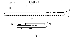
Fig. 1 is the figure of schematic configuration of the optical-electricity encoder 1 of expression the 1st embodiment.Present embodiment is a principal character with the structure of the light-receiving chip that comprises in light receiver, as the prerequisite of this understanding, optical-electricity encoder 1 is described.The structure of scrambler 1 at first, is described.Scrambler 1 constitutes by light emitting diode (LED (light emitting diode)) 3 and with the scale 5 of the arranged in order close with it and light receiver 7.
Light receiver 7 and scale 5 (gap) configuration at interval.Light receiver 7 comprises light-receiving chip 15 that is positioned at scale 5 sides and the circuitry substrate 17 of carrying it.In light-receiving chip 15, form not shown a plurality of photodiodes (below, sometimes ' photodiode ' is recited as ' PD ').Each light receiving surface of these PD is towards the 1st optical lattice 11 sides.PD is an example of light receiving element.As light receiving element, also can use phototransistor to replace PD.In circuitry substrate 17, carry the IC chip 19 that is used for computing.IC chip 19 is carried out the computing of displacement according to the detected light signal of a plurality of PD of light-receiving chip 15.
Light receiver 7 is installed on the support (holder) 21 with light emitting diode 3.Support 21 is removable on the longitudinal direction with the scale shown in the X 5 in the drawings.That is, optical-electricity encoder 1 is measured displacement by with respect to fixing scale 5 traversing carriages 21.Therefore, directions X for measure axle (below, with directions X as ' measure an X ').Have again,, scale 5 is moved in the type of measuring displacement, also can adopt the present invention in that light emitting diode 3 and light receiver 7 is fixing.Therefore, the light receiver 7 that will comprise light-receiving chip 15 is configured to and can relatively moves measuring on the axle directions X with respect to scale 5 with light emitting diode 3.
Below, the mensuration action of briefly bright optical-electricity encoder 1.When light emitting diode 3 shines the 1st optical lattice 11 of scale 5 with light L, on light-receiving chip 15, produce shading graphic by the 1st optical lattice 11.This shading graphic is irradiated on the light-receiving chip 15.In this state, detect by support 21 along measuring the variation (sinusoidal wave light signal) that axle X moves the shading graphic of generation by each photodiode (PD) that is formed at light-receiving chip 15.That is, the light signal of A phase (0 degree), phase place than B phase (90 degree) light signal of A phase deviation 90 degree, phase place than the light signal of the AA phase (180 degree) of A phase deviation 180 degree and phase place than the BB of A phase deviation 270 degree mutually the light signal of (270 degree) detect by the PD of correspondence respectively.Like this, each PD is received in the light signal of the phase place that is assigned with in the different a plurality of light signals of phase place.
Electric signal by each light signal generating is sent to IC chip 19.In IC chip 19, A mutually and after B carries out predetermined process (removing DC component etc.) mutually, is being come the computing displacement according to the A phase after handling with B mutually.Its result is outputed to not shown display part.It more than is the action of optical-electricity encoder 1.
The principal character of the 1st embodiment is a light-receiving chip 15, below it is explained.The planar structure of light-receiving chip 15 at first, is described.Fig. 2 is the planimetric map of schematically representing from light-receiving chip 15 integral body of the 1st optical lattice side observation.Fig. 3 is the figure of photodiode 23 in the presentation graphs 2 schematically.Fig. 4 is the figure of the 2nd optical lattice 25 in the presentation graphs 2 schematically.
With reference to Fig. 2~Fig. 4, cover the light receiving surface 27 of a plurality of PD23 and light receiving surface 27 and the 2nd optical lattice 25 that forms is configured in the face of on the xy face of the 1st optical lattice.Have, the x axle is consistent with mensuration axle directions X illustrated in fig. 1 again.The 2nd optical lattice 25 has a plurality of light shielding parts 29 that prolong on the y direction of arranged spaced on each light receiving surface 27.
Incide corresponding light receiving surface 27 based on four different (A phase, B phase, AA phase, BB phase) light signals of the phase place of the photogenerated that shines the 1st optical lattice.In other words, under above-mentioned shading graphic is irradiated to state on the light-receiving chip 15, each light receiving surface 27 of light signal incident of the phase place that is assigned with in the different a plurality of light signals of the phase place that generates by traversing carriage 21.Thus, four light signals that phase place is different are detected by a plurality of PD23.To detect the group of PD23A, 23B, 23AA, 23BB of the light signal of A phase, B phase, AA phase, BB phase respectively along measuring an axle X repeated configuration.
Also can following explanation rake 33.With the pair of angled portion 33 that comprises in the light receiving surface 27 with respect to measuring axle X with identical size tilted configuration reciprocally.Extending direction and a mensuration axle X with respect to light shielding part 29 disposes obliquely with rake 33 (that is at least a portion of each light receiving surface 27).
In the arrangement of a plurality of PD23, the set of the PD23 that the right half part of pie graph 3 is arranged is the 1st element group 35, and the set that constitutes the PD23 of left-half arrangement is the 2nd element group 37.The 1st element group 35 and the 2nd element group 37 have protuberance 36 along measuring axle X respectively at one end, recess 38 is arranged on the other end.The recess 38 of the 1st element group 35 and the recess 38 of the 2nd element group 37 are configured on the xy face in opposed facing mode.
Fig. 5 has amplified the zone of representing with V of Fig. 2.Light shielding part 29 interval in accordance with regulations is formed on each light receiving surface 27.The space phase of the light shielding part 29 of the 2nd optical lattice 25 of configuration is different mutually on the light receiving surface 27 of adjacent PD23.Specifically, on adjacent light receiving surface 27, light shielding part 29 disposes along measuring axle X skew λ/4.Here, λ is the wavelength of light signal.Fig. 6 is a synoptic diagram of observing the zone of Fig. 5 from VI (a)-VI (b) section.Light-receiving chip 15 comprises the Semiconductor substrate of n type.In a face of this substrate 39, form the diffusion zone 41 of p type at interval.The junction surface of Semiconductor substrate 39 and diffusion zone 41 is PD23.A plurality of PD23 shown in Figure 3 along being formed in the Semiconductor substrate 39 with measuring axle X array-like.In a face of Semiconductor substrate 39, the zone that has formed p type diffusion zone 41 is a light receiving surface 27.In diffusion zone 41 Semiconductor substrate 39 each other, form n
+The diffusion zone 43 of type.Thus, p type diffusion zone 41 separates with adjacent diffusion zone 41, that is, each PD23 is separated by element.
The such dielectric film 45 of an oxidized silicon fiml of face of Semiconductor substrate 39 covers, to cover diffusion zone 41,43.On dielectric film 45, form a plurality of light shielding parts 29 at interval.As long as light shielding part 29 has lighttight character, so its material can list metal (for example, chromium, aluminium) or resin.In order to cover these light shielding parts 29, form silicon oxide film and the such diaphragm 47 of silicon nitride film.On whole of the another side of Semiconductor substrate 39, form the common electrode (for example Au electrode) 49 of each PD23.
The following describes the effect of the optical-electricity encoder 1 of the 1st embodiment.
(1), can obtain the mensuration precision under the two-dimensional arrangement situation by the response speed of the scrambler under the one dimension configuring condition of photodiode according to the 1st embodiment.Explain with Fig. 2~Fig. 4 below.Photodiode 23 is along measuring axle X configuration.Therefore, the PD23 of scrambler 1 is the one dimension configuration, so can suppress the increase of the junction capacity of PD23.On the other hand, the rake 33 of light receiving surface 27 tilts with respect to the extending direction (y direction) of the light shielding part 29 of the 2nd optical lattice 25, so rake 33 forms two-dimensional arrangement with the extending direction (y direction) of measuring axle directions X (x direction) and light shielding part 29.Therefore, according to scrambler 1, can obtain the average effect same with the two-dimensional arrangement of photodiode.
As mentioned above, according to the 1st embodiment, the total of the junction capacity of a plurality of photodiodes is identical with the one dimension configuration, can obtain the average effect same with the two-dimensional arrangement of photodiode simultaneously.Therefore, the response speed that can take into account scrambler 1 improves and the raising of mensuration precision.
Above-mentioned effect is produced by rake 33, so can not comprise that parallel portion 31 times constitutes light receiving surface 27 by pair of angled portion 33, also can be only constitutes light receiving surface 27 by a side of pair of angled portion 33.
(2) as shown in Figure 3, according to the 1st embodiment, a plurality of PD23 are divided into the 1st element group 35 and the 2nd element group 37.Then, on the xy face, the recess 38 of the recess 38 of the 1st element group 35 and the 2nd element group 37 faced mutually dispose.Therefore, the shape that is made of the light receiving surface 27 of a plurality of PD23 is the shape of symmetry with respect to x direction and y direction.Therefore, the light receiving surface of a plurality of PD23 balancedly can be configured on the xy face in 270 minutes.
Have again, as shown in Figure 7, dispose even the protuberance 36 of the protuberance 36 of the 1st element group 35 and the 2nd element group 37 faced mutually, also same with Fig. 3, can very balancedly dispose the light receiving surface 27 of a plurality of PD23.
The 2nd embodiment
Relevant the 2nd embodiment is that the center illustrates with the difference with the 1st embodiment.Fig. 8 is the planimetric map that schematically is illustrated in the part of the light-receiving chip of being furnished with in the optical-electricity encoder of the 2nd embodiment 15, and is corresponding with Fig. 5.Fig. 9, Figure 10 are the synoptic diagram of observing the light-receiving chip 15 of Fig. 8 respectively from IX (a)-IX (b), X (a)-X (b) section.In the 2nd embodiment, with the light shielding part 29 of the 2nd optical lattice a part as the wiring 51 that is connected to photodiode 23.Below, explain.
The 2nd embodiment except have with the same effect of the 1st embodiment, also have following effect.To be connected with photodiode in order connecting up, on the light receiving surface 27 of the layer identical, to form under the situation of new conductive film structure, reduce effective light receiving area of light receiving surface 27 because of this conducting film with light shielding part 29.On the contrary, in the 2nd embodiment, at wiring 51 and the light shielding part 29 that being connected of photodiode 23 utilizes electric conductivity.Therefore, can prevent the minimizing of effective light receiving area of light receiving surface 27.
In addition, under the situation that has formed above-mentioned new conductive film structure, in the section of Figure 10, there is not contact site 55.Therefore, form the stray capacitance that clips dielectric film 45 structures by light shielding part 29 and diffusion zone 41.This becomes the reason of the response speed that reduces scrambler.On the contrary, in the 2nd embodiment, because light shielding part 29 is connected with diffusion zone 41 usefulness contact sites 55, so do not produce stray capacitance as described above.
Have again, in the 1st and the 2nd embodiment, use four different light signals (light signal of A phase, B phase, AA phase, BB phase) of phase place to measure displacement, but optical-electricity encoder of the present invention is not limited thereto.For example, for three light signals (light signal of phase place 0 degree, phase place are spent the light signals of skew 120 degree, the light signal that phase place is spent than 0 degree skew 240 than 0) that phase place is different, also go for optical-electricity encoder of the present invention.
In addition, as shown in Figure 1, the optical-electricity encoder 1 of the 1st and the 2nd embodiment is to use the type of carrying out the so-called infiltration type of displacement mensuration through the light L from light emitting diode 3 of the 1st optical lattice 11 of scale 5.But, the type of reflection-type, that is, the light L from light emitting diode 3 by the 1st optical lattice 11 reflections of scale 5 measures under the situation of displacement in use, also can adopt the present invention.
As previously discussed, according to optical-electricity encoder of the present invention, the total of the junction capacity of a plurality of light receiving elements is identical with the one dimension configuration, can obtain the average effect same with the two-dimensional arrangement of light receiving element simultaneously.Therefore, can take into account optical-electricity encoder response speed raising and measure the raising of precision.
Claims (6)
1. optical-electricity encoder comprises:
Light source;
Scale, it comprises by light-struck the 1st optical lattice from described light source;
A plurality of light receiving elements comprise the light receiving surface of incident based on the light signal that light generated that shines described the 1st optical lattice respectively, and the different a plurality of light signals of detected phase; And
The 2nd optical lattice comprises the light shielding part on each light receiving surface that is configured in described a plurality of light receiving elements;
It is characterized in that described a plurality of light receiving elements are configured to described relatively scale and can relatively move along measuring axle, simultaneously along the configuration of described mensuration axle, each light receiving surface are tilted with respect to the extending direction of described light shielding part.
2. optical-electricity encoder as claimed in claim 1 is characterized in that:
By described a plurality of light receiving elements, on the plane that has disposed described a plurality of light receiving elements, constituting along described axle one end of measuring has protuberance, the other end that the 1st and the 2nd element group of recess is arranged,
Described the 1st element group and described the 2nd element assembly be changed to described recess each other or protuberance on described plane, face mutually each other.
3. optical-electricity encoder as claimed in claim 1 is characterized in that:
Be furnished with the light-receiving chip that comprises described a plurality of light receiving element and described the 2nd optical lattice,
Described light-receiving chip also comprises:
Contact site, it is provided with respectively with respect to described a plurality of light receiving elements, is connected to this light shielding part below the described light shielding part of electric conductivity, contacts with described light receiving surface simultaneously; And
The wiring of described light receiving element, it is provided with respectively with respect to described a plurality of light receiving elements, is connected with described light shielding part.
4. optical-electricity encoder as claimed in claim 1 is characterized in that, the spatiality phase place of the described light shielding part of described the 2nd optical lattice that disposes on the light receiving surface of adjacent light receiving element in described a plurality of light receiving elements is different mutually.
5. optical-electricity encoder as claimed in claim 1 is characterized in that, the part of described light receiving surface is configured to tilt with respect to the extending direction of described light shielding part along the described axle of measuring.
6. optical-electricity encoder as claimed in claim 1 is characterized in that, the whole of described light receiving surface are configured to tilt with respect to the extending direction of described light shielding part along the described axle of measuring.
Applications Claiming Priority (3)
| Application Number | Priority Date | Filing Date | Title |
|---|---|---|---|
| JP2003139061A JP4350419B2 (en) | 2003-05-16 | 2003-05-16 | Photoelectric encoder |
| JP139061/03 | 2003-05-16 | ||
| JP139061/2003 | 2003-05-16 |
Publications (2)
| Publication Number | Publication Date |
|---|---|
| CN1550760A CN1550760A (en) | 2004-12-01 |
| CN100335863C true CN100335863C (en) | 2007-09-05 |
Family
ID=33095368
Family Applications (1)
| Application Number | Title | Priority Date | Filing Date |
|---|---|---|---|
| CNB2004100432957A Active CN100335863C (en) | 2003-05-16 | 2004-05-17 | Photoelectric encoder |
Country Status (6)
| Country | Link |
|---|---|
| US (1) | US7095011B2 (en) |
| EP (1) | EP1480017B2 (en) |
| JP (1) | JP4350419B2 (en) |
| CN (1) | CN100335863C (en) |
| AT (1) | ATE309523T1 (en) |
| DE (1) | DE602004000174T3 (en) |
Families Citing this family (4)
| Publication number | Priority date | Publication date | Assignee | Title |
|---|---|---|---|---|
| JP4908329B2 (en) * | 2007-06-28 | 2012-04-04 | 株式会社リコー | MOVING SPEED CONTROL DEVICE FOR Detected Object, Manufacturing Method for Optical Encoder, and Image Forming Apparatus |
| US7612326B2 (en) * | 2007-08-27 | 2009-11-03 | Delta Electronics Inc. | Angle-calculation apparatus and angle-calculation method for three-phase optical encoder |
| JP6197480B2 (en) * | 2013-08-23 | 2017-09-20 | オムロン株式会社 | Shielding plate for optical encoder, method for manufacturing the same, and optical encoder using the same |
| DE102018109615A1 (en) * | 2018-04-20 | 2019-10-24 | Carmar Accuracy Co., Ltd. | Sensor chip of a reading head of an optical ruler |
Citations (6)
| Publication number | Priority date | Publication date | Assignee | Title |
|---|---|---|---|---|
| DE1282988B (en) * | 1965-05-28 | 1968-11-14 | Zeiss Carl Fa | Device for measuring changes in position of two mutually movable parts using incoherent radiation |
| CN1014935B (en) * | 1988-01-22 | 1991-11-27 | 株式会社三丰 | Optical encoder |
| CN1017658B (en) * | 1988-01-22 | 1992-07-29 | 株式会社三丰 | Optical encoder |
| JPH07151565A (en) * | 1993-11-26 | 1995-06-16 | Mitsutoyo Corp | Photoelectric encoder |
| US5841133A (en) * | 1996-10-28 | 1998-11-24 | Mitutoyo Corporation | Optical displacement detecting apparatus having gratings and a light receiving chip |
| WO2001031292A1 (en) * | 1999-10-26 | 2001-05-03 | Citizen Watch Co., Ltd. | Optical displacement measuring device |
Family Cites Families (5)
| Publication number | Priority date | Publication date | Assignee | Title |
|---|---|---|---|---|
| DE2500798A1 (en) † | 1975-01-10 | 1976-07-15 | Leitz Ernst Gmbh | OPTICAL MEASURING SYSTEM |
| DE59105197D1 (en) † | 1991-11-04 | 1995-05-18 | Heidenhain Gmbh Dr Johannes | Device for generating harmonic-free periodic signals. |
| DE4323624C2 (en) † | 1993-07-15 | 1997-09-11 | Heidenhain Gmbh Dr Johannes | Photoelectric length or angle measuring device |
| GB9928483D0 (en) * | 1999-12-03 | 2000-02-02 | Renishaw Plc | Opto-electronic scale reading apparatus |
| DE10022619A1 (en) † | 2000-04-28 | 2001-12-06 | Heidenhain Gmbh Dr Johannes | Scanning unit for an optical position measuring device |
-
2003
- 2003-05-16 JP JP2003139061A patent/JP4350419B2/en not_active Expired - Fee Related
-
2004
- 2004-05-14 US US10/846,437 patent/US7095011B2/en active Active
- 2004-05-17 DE DE602004000174T patent/DE602004000174T3/en active Active
- 2004-05-17 AT AT04011685T patent/ATE309523T1/en not_active IP Right Cessation
- 2004-05-17 EP EP04011685A patent/EP1480017B2/en active Active
- 2004-05-17 CN CNB2004100432957A patent/CN100335863C/en active Active
Patent Citations (6)
| Publication number | Priority date | Publication date | Assignee | Title |
|---|---|---|---|---|
| DE1282988B (en) * | 1965-05-28 | 1968-11-14 | Zeiss Carl Fa | Device for measuring changes in position of two mutually movable parts using incoherent radiation |
| CN1014935B (en) * | 1988-01-22 | 1991-11-27 | 株式会社三丰 | Optical encoder |
| CN1017658B (en) * | 1988-01-22 | 1992-07-29 | 株式会社三丰 | Optical encoder |
| JPH07151565A (en) * | 1993-11-26 | 1995-06-16 | Mitsutoyo Corp | Photoelectric encoder |
| US5841133A (en) * | 1996-10-28 | 1998-11-24 | Mitutoyo Corporation | Optical displacement detecting apparatus having gratings and a light receiving chip |
| WO2001031292A1 (en) * | 1999-10-26 | 2001-05-03 | Citizen Watch Co., Ltd. | Optical displacement measuring device |
Also Published As
| Publication number | Publication date |
|---|---|
| ATE309523T1 (en) | 2005-11-15 |
| EP1480017B2 (en) | 2009-09-02 |
| DE602004000174T2 (en) | 2006-05-24 |
| JP2004340815A (en) | 2004-12-02 |
| DE602004000174T3 (en) | 2009-12-17 |
| CN1550760A (en) | 2004-12-01 |
| DE602004000174D1 (en) | 2005-12-15 |
| EP1480017B1 (en) | 2005-11-09 |
| JP4350419B2 (en) | 2009-10-21 |
| US20040238728A1 (en) | 2004-12-02 |
| US7095011B2 (en) | 2006-08-22 |
| EP1480017A1 (en) | 2004-11-24 |
Similar Documents
| Publication | Publication Date | Title |
|---|---|---|
| CN100351613C (en) | Photoelectric encoder | |
| CN1324303C (en) | Photoelectric encoder | |
| JP5974329B2 (en) | Photoelectric encoder | |
| GB2254690A (en) | Two-dimensional three-grating optical encoder | |
| CN100335863C (en) | Photoelectric encoder | |
| JP4834141B2 (en) | Photoelectric encoder | |
| JP4546485B2 (en) | Scan head for optical position measurement system | |
| JP4265928B2 (en) | Photoelectric encoder | |
| JP4372566B2 (en) | Photoelectric encoder | |
| JP2571694B2 (en) | Light receiving position detecting device using optical fiber for level survey staff | |
| CN1260870A (en) | Position detection apparatus | |
| CN1815262A (en) | Optical mobile sensing module and its optical mobile sensor | |
| CN1542411A (en) | Optical semiconductor device | |
| JPS63249003A (en) | Detection of position of light reception using optical fiber |
Legal Events
| Date | Code | Title | Description |
|---|---|---|---|
| C06 | Publication | ||
| PB01 | Publication | ||
| C10 | Entry into substantive examination | ||
| SE01 | Entry into force of request for substantive examination | ||
| C14 | Grant of patent or utility model | ||
| GR01 | Patent grant |