BR112016000868B1 - COMPLETE SYSTEM-ON-CHIP (SOC) USING THREE-DIMENSIONAL (3D) (3DIC) MONOLITHIC INTEGRATED CIRCUIT (IC) TECHNOLOGY - Google Patents
COMPLETE SYSTEM-ON-CHIP (SOC) USING THREE-DIMENSIONAL (3D) (3DIC) MONOLITHIC INTEGRATED CIRCUIT (IC) TECHNOLOGY Download PDFInfo
- Publication number
- BR112016000868B1 BR112016000868B1 BR112016000868-5A BR112016000868A BR112016000868B1 BR 112016000868 B1 BR112016000868 B1 BR 112016000868B1 BR 112016000868 A BR112016000868 A BR 112016000868A BR 112016000868 B1 BR112016000868 B1 BR 112016000868B1
- Authority
- BR
- Brazil
- Prior art keywords
- levels
- 3dic
- soc
- level
- layers
- Prior art date
Links
Images


Classifications
-
- H—ELECTRICITY
- H01—ELECTRIC ELEMENTS
- H01L—SEMICONDUCTOR DEVICES NOT COVERED BY CLASS H10
- H01L27/00—Devices consisting of a plurality of semiconductor or other solid-state components formed in or on a common substrate
- H01L27/02—Devices consisting of a plurality of semiconductor or other solid-state components formed in or on a common substrate including semiconductor components specially adapted for rectifying, oscillating, amplifying or switching and having at least one potential-jump barrier or surface barrier; including integrated passive circuit elements with at least one potential-jump barrier or surface barrier
- H01L27/04—Devices consisting of a plurality of semiconductor or other solid-state components formed in or on a common substrate including semiconductor components specially adapted for rectifying, oscillating, amplifying or switching and having at least one potential-jump barrier or surface barrier; including integrated passive circuit elements with at least one potential-jump barrier or surface barrier the substrate being a semiconductor body
- H01L27/06—Devices consisting of a plurality of semiconductor or other solid-state components formed in or on a common substrate including semiconductor components specially adapted for rectifying, oscillating, amplifying or switching and having at least one potential-jump barrier or surface barrier; including integrated passive circuit elements with at least one potential-jump barrier or surface barrier the substrate being a semiconductor body including a plurality of individual components in a non-repetitive configuration
- H01L27/0688—Integrated circuits having a three-dimensional layout
-
- H—ELECTRICITY
- H01—ELECTRIC ELEMENTS
- H01L—SEMICONDUCTOR DEVICES NOT COVERED BY CLASS H10
- H01L25/00—Assemblies consisting of a plurality of individual semiconductor or other solid state devices ; Multistep manufacturing processes thereof
- H01L25/18—Assemblies consisting of a plurality of individual semiconductor or other solid state devices ; Multistep manufacturing processes thereof the devices being of types provided for in two or more different subgroups of the same main group of groups H01L27/00 - H01L33/00, or in a single subclass of H10K, H10N
-
- H—ELECTRICITY
- H01—ELECTRIC ELEMENTS
- H01L—SEMICONDUCTOR DEVICES NOT COVERED BY CLASS H10
- H01L21/00—Processes or apparatus adapted for the manufacture or treatment of semiconductor or solid state devices or of parts thereof
- H01L21/70—Manufacture or treatment of devices consisting of a plurality of solid state components formed in or on a common substrate or of parts thereof; Manufacture of integrated circuit devices or of parts thereof
- H01L21/77—Manufacture or treatment of devices consisting of a plurality of solid state components or integrated circuits formed in, or on, a common substrate
- H01L21/78—Manufacture or treatment of devices consisting of a plurality of solid state components or integrated circuits formed in, or on, a common substrate with subsequent division of the substrate into plural individual devices
- H01L21/82—Manufacture or treatment of devices consisting of a plurality of solid state components or integrated circuits formed in, or on, a common substrate with subsequent division of the substrate into plural individual devices to produce devices, e.g. integrated circuits, each consisting of a plurality of components
- H01L21/822—Manufacture or treatment of devices consisting of a plurality of solid state components or integrated circuits formed in, or on, a common substrate with subsequent division of the substrate into plural individual devices to produce devices, e.g. integrated circuits, each consisting of a plurality of components the substrate being a semiconductor, using silicon technology
- H01L21/8221—Three dimensional integrated circuits stacked in different levels
-
- H—ELECTRICITY
- H01—ELECTRIC ELEMENTS
- H01L—SEMICONDUCTOR DEVICES NOT COVERED BY CLASS H10
- H01L23/00—Details of semiconductor or other solid state devices
- H01L23/48—Arrangements for conducting electric current to or from the solid state body in operation, e.g. leads, terminal arrangements ; Selection of materials therefor
- H01L23/481—Internal lead connections, e.g. via connections, feedthrough structures
-
- H—ELECTRICITY
- H01—ELECTRIC ELEMENTS
- H01L—SEMICONDUCTOR DEVICES NOT COVERED BY CLASS H10
- H01L2224/00—Indexing scheme for arrangements for connecting or disconnecting semiconductor or solid-state bodies and methods related thereto as covered by H01L24/00
- H01L2224/01—Means for bonding being attached to, or being formed on, the surface to be connected, e.g. chip-to-package, die-attach, "first-level" interconnects; Manufacturing methods related thereto
- H01L2224/10—Bump connectors; Manufacturing methods related thereto
- H01L2224/15—Structure, shape, material or disposition of the bump connectors after the connecting process
- H01L2224/16—Structure, shape, material or disposition of the bump connectors after the connecting process of an individual bump connector
- H01L2224/161—Disposition
- H01L2224/16135—Disposition the bump connector connecting between different semiconductor or solid-state bodies, i.e. chip-to-chip
- H01L2224/16145—Disposition the bump connector connecting between different semiconductor or solid-state bodies, i.e. chip-to-chip the bodies being stacked
-
- H—ELECTRICITY
- H01—ELECTRIC ELEMENTS
- H01L—SEMICONDUCTOR DEVICES NOT COVERED BY CLASS H10
- H01L2224/00—Indexing scheme for arrangements for connecting or disconnecting semiconductor or solid-state bodies and methods related thereto as covered by H01L24/00
- H01L2224/01—Means for bonding being attached to, or being formed on, the surface to be connected, e.g. chip-to-package, die-attach, "first-level" interconnects; Manufacturing methods related thereto
- H01L2224/10—Bump connectors; Manufacturing methods related thereto
- H01L2224/15—Structure, shape, material or disposition of the bump connectors after the connecting process
- H01L2224/16—Structure, shape, material or disposition of the bump connectors after the connecting process of an individual bump connector
- H01L2224/161—Disposition
- H01L2224/16151—Disposition the bump connector connecting between a semiconductor or solid-state body and an item not being a semiconductor or solid-state body, e.g. chip-to-substrate, chip-to-passive
- H01L2224/16221—Disposition the bump connector connecting between a semiconductor or solid-state body and an item not being a semiconductor or solid-state body, e.g. chip-to-substrate, chip-to-passive the body and the item being stacked
- H01L2224/16225—Disposition the bump connector connecting between a semiconductor or solid-state body and an item not being a semiconductor or solid-state body, e.g. chip-to-substrate, chip-to-passive the body and the item being stacked the item being non-metallic, e.g. insulating substrate with or without metallisation
-
- H—ELECTRICITY
- H01—ELECTRIC ELEMENTS
- H01L—SEMICONDUCTOR DEVICES NOT COVERED BY CLASS H10
- H01L2224/00—Indexing scheme for arrangements for connecting or disconnecting semiconductor or solid-state bodies and methods related thereto as covered by H01L24/00
- H01L2224/01—Means for bonding being attached to, or being formed on, the surface to be connected, e.g. chip-to-package, die-attach, "first-level" interconnects; Manufacturing methods related thereto
- H01L2224/42—Wire connectors; Manufacturing methods related thereto
- H01L2224/47—Structure, shape, material or disposition of the wire connectors after the connecting process
- H01L2224/48—Structure, shape, material or disposition of the wire connectors after the connecting process of an individual wire connector
- H01L2224/4805—Shape
- H01L2224/4809—Loop shape
- H01L2224/48091—Arched
-
- H—ELECTRICITY
- H01—ELECTRIC ELEMENTS
- H01L—SEMICONDUCTOR DEVICES NOT COVERED BY CLASS H10
- H01L2225/00—Details relating to assemblies covered by the group H01L25/00 but not provided for in its subgroups
- H01L2225/03—All the devices being of a type provided for in the same subgroup of groups H01L27/00 - H01L33/648 and H10K99/00
- H01L2225/04—All the devices being of a type provided for in the same subgroup of groups H01L27/00 - H01L33/648 and H10K99/00 the devices not having separate containers
- H01L2225/065—All the devices being of a type provided for in the same subgroup of groups H01L27/00 - H01L33/648 and H10K99/00 the devices not having separate containers the devices being of a type provided for in group H01L27/00
- H01L2225/06503—Stacked arrangements of devices
- H01L2225/06541—Conductive via connections through the device, e.g. vertical interconnects, through silicon via [TSV]
- H01L2225/06544—Design considerations for via connections, e.g. geometry or layout
-
- H—ELECTRICITY
- H01—ELECTRIC ELEMENTS
- H01L—SEMICONDUCTOR DEVICES NOT COVERED BY CLASS H10
- H01L25/00—Assemblies consisting of a plurality of individual semiconductor or other solid state devices ; Multistep manufacturing processes thereof
- H01L25/03—Assemblies consisting of a plurality of individual semiconductor or other solid state devices ; Multistep manufacturing processes thereof all the devices being of a type provided for in the same subgroup of groups H01L27/00 - H01L33/00, or in a single subclass of H10K, H10N, e.g. assemblies of rectifier diodes
- H01L25/04—Assemblies consisting of a plurality of individual semiconductor or other solid state devices ; Multistep manufacturing processes thereof all the devices being of a type provided for in the same subgroup of groups H01L27/00 - H01L33/00, or in a single subclass of H10K, H10N, e.g. assemblies of rectifier diodes the devices not having separate containers
- H01L25/065—Assemblies consisting of a plurality of individual semiconductor or other solid state devices ; Multistep manufacturing processes thereof all the devices being of a type provided for in the same subgroup of groups H01L27/00 - H01L33/00, or in a single subclass of H10K, H10N, e.g. assemblies of rectifier diodes the devices not having separate containers the devices being of a type provided for in group H01L27/00
- H01L25/0657—Stacked arrangements of devices
Abstract
SISTEMA-EM-CHIP (SOC) COMPLETO USANDO TECNOLOGIA DE CIRCUITO INTEGRADO (IC) TRIDIMENSIONAL (3D) (3DI C) MONOLÍTICO. Formas de realização na descrição detalhada incluem uma solução de sistema-em-chip (SOC) completo usando tecnologia de integração de circuito integra do (IC) tridimensional (3D) (3DIC) monolítico. A presente invenção inclui exemplo da capacidade de personalizar camadas dentro de um 3DIC monolítico e as interligações curtas anexas possíveis entre fileiras através de vias entre níveis monolíticos (MIV) para criar um sistema em um chip. Em particular, diferentes níveis do 3DIC são construídos para suportar diferentes funcionalidades e atender diferentes critérios de design. Assim, o 3DIC pode ter uma camada analógica, camadas com limite de tensão mais elevado, camadas com menor corrente de fuga, camadas de material diferente para implementar componentes que precisam de diferentes materiais de base e similares. Ao contrário das matrizes empilhadas, as camadas superiores podem ser do mesmo tamanho que as camadas inferiores porque não são necessárias ligações de cabos externos.COMPLETE SYSTEM-ON-CHIP (SOC) USING THREE-DIMENSIONAL (3D) (3DI C) MONOLITHIC INTEGRATED CIRCUIT (IC) TECHNOLOGY. Embodiments in the detailed description include a complete system-on-chip (SOC) solution using monolithic three-dimensional (3D) integrated circuit (IC) (3DIC) integration technology. The present invention includes an example of the ability to customize layers within a monolithic 3DIC and the attached short inter-tier interconnections possible via monolithic inter-level pathways (MIV) to create a system on a chip. In particular, different levels of 3DIC are built to support different functionality and meet different design criteria. So 3DIC can have an analog layer, layers with higher voltage threshold, layers with lower leakage current, layers of different material to implement components that need different base materials and the like. Unlike stacked dies, the top layers can be the same size as the bottom layers because no external cable connections are required.
Description
[0001] O presente pedido reivindica prioridade ao Pedido de Patente Provisório número de série 61/846.648 depositado em 16 de julho de 2013 e intitulado “COMPLETE SYSTEM-ON-CHIP (SOC) USING MONOLITHIC THREE DIMENSIONAL (3D) INTEGRATED CIRCUIT (IC) (3DIC) TECHNOLOGY”, que é aqui incorporado por referência em sua totalidade.[0001] The present application claims priority to Provisional Patent Application serial number 61/846,648 filed on July 16, 2013 and entitled “COMPLETE SYSTEM-ON-CHIP (SOC) USING MONOLITHIC THREE DIMENSIONAL (3D) INTEGRATED CIRCUIT (IC) (3DIC) TECHNOLOGY”, which is incorporated herein by reference in its entirety.
[0002] O presente pedido de patente também reivindica prioridade ao Pedido de Patente US número de série 14/013.399 depositado em 29 de agosto de 2013 e intitulada “COMPLETE SYSTEM-ON-CHIP (SOC) USING MONOLITHIC THREE DIMENSIONAL (3D) INTEGRATED CIRCUIT (IC) (3DIC) TECHNOLOGY”, que é aqui incorporado por referência em sua totalidade.[0002] The present patent application also claims priority to US Patent
[0003] A tecnologia da divulgação se refere em geral a circuitos integrados (ICs) de sistema-em-chip (SOC).[0003] The technology of the disclosure generally refers to system-on-chip (SOC) integrated circuits (ICs).
[0004] Dispositivos de comunicações móveis tornaram-se comuns na sociedade atual. A prevalência desses dispositivos móveis é impulsionada em parte pelas muitas funções que agora são possibilitadas em tais dispositivos. A demanda por tais funções aumenta as necessidades de capacidade de processamento e gera uma necessidade de baterias mais potentes. Dentro do espaço limitado do alojamento do dispositivo de comunicação móvel, baterias competem com os circuitos de processamento. A pressão do espaço limitado contribui para uma miniaturização continuada dos componentes e o consumo de energia dentro dos circuitos. Embora a miniaturização tenha sido uma preocupação especial nos circuitos integrados (ICs) de dispositivos de comunicação móvel, esforços de miniaturização dos ICs em outros dispositivos também têm acontecido.[0004] Mobile communications devices have become commonplace in today's society. The prevalence of these mobile devices is driven in part by the many functions that are now made possible on such devices. Demand for such functions increases processing power needs and creates a need for more powerful batteries. Within the limited space of the mobile communication device housing, batteries compete with the processing circuits. The pressure of limited space contributes to continued miniaturization of components and energy consumption within circuits. While miniaturization has been a particular concern in the integrated circuits (ICs) of mobile communication devices, efforts to miniaturize ICs in other devices have also taken place.
[0005] Esforços crescentes têm sido feitos em miniaturizar os componentes digitais e apertar cada vez mais funções digitais em um único circuito integrado (IC). No entanto, até o momento, tem-se revelado difícil incluir ambos componentes analógicos como digitais dentro de um único IC, tal como, por exemplo, na concepção de um transceptor de frequência de rádio (RF) e o elemento de processamento de sinal para um telefone celular ou outro dispositivo de comunicação móvel. Da mesma forma, mesmo dentro do mesmo lado da moeda digital / analógica, às vezes pode ser difícil incorporar componentes com requisitos físicos díspares em um único IC. Por exemplo, elementos com uma exigência de alta velocidade podem ser difíceis de integrar no mesmo chip com elementos que requerem baixa fuga de corrente. Esta dificuldade em unir esses elementos em um único chip tornou impraticáveis verdadeiras soluções de sistema-em-chip (SOC). Na maioria dos dispositivos, um chip analógico é criado e eletricamente acoplado a um chip digital. O acoplamento requer condutores elétricos e resulta em uma severa penalidade de área, visto que o espaço dentro do dispositivo é dedicado a esses condutores. O uso de tal espaço para condutores colide com os objetivos gerais de miniaturização.[0005] Increasing efforts have been made to miniaturize digital components and squeeze more and more digital functions into a single integrated circuit (IC). However, until now, it has proved difficult to include both analog and digital components within a single IC, such as, for example, in the design of a radio frequency (RF) transceiver and the signal processing element for a cell phone or other mobile communication device. Likewise, even within the same side of the digital/analog coin, it can sometimes be difficult to incorporate components with disparate physical requirements into a single IC. For example, elements with a high speed requirement can be difficult to integrate on the same chip with elements that require low leakage current. This difficulty in bringing these elements together on a single chip has made true system-on-chip (SOC) solutions impractical. In most devices, an analog chip is created and electrically coupled to a digital chip. Coupling requires electrical conductors and results in a severe area penalty as space within the device is dedicated to these conductors. The use of such space for conductors clashes with the general goals of miniaturization.
[0006] Uma solução de compromisso para estes critérios de design concorrentes tem sido design de empilhamento de matriz ou outro sistema em montagens de encapsulamento (SIP). Em tais montagens de empilhamento de matriz, uma matriz digital é empilhada em cima de uma matriz analógica ou vice-versa. No entanto, o espaço ainda é gasto interconectando as matrizes. Da mesma forma, a matriz superior é geralmente menor do que a matriz inferior, formando uma forma semelhante a um zigurate. Embora existam implementações comerciais que têm até três matrizes empilhadas umas sobre as outras, essas implementações não têm substanciais economias de espaço. Assim, permanece a necessidade de um SOC verdadeiramente integrado.[0006] A compromise solution to these competing design criteria has been array stacking design or other system in encapsulation (SIP) assemblies. In such matrix-stacking assemblies, a digital matrix is stacked on top of an analog matrix or vice versa. However, space is still spent interconnecting the arrays. Likewise, the top die is usually smaller than the bottom die, forming a ziggurat-like shape. While there are commercial implementations that have up to three arrays stacked on top of each other, these implementations do not have substantial space savings. Thus, the need for a truly integrated SOC remains.
[0007] As formas de realização descritas na descrição detalhada incluem uma solução de sistema-em-chip completa utilizando tecnologia de integração de circuito integrado (IC) tridimensional (3D) (3DIC) monolítico. A presente divulgação inclui exemplos da capacidade de personalizar camadas dentro de um 3DIC monolítico e as interligações curtas anexas possíveis entre níveis através de vias entre níveis monolíticos (MIV) para criar um “sistema em um chip” ou “sistema-em-chip”, ambos referidos como (SOC). Em especial, diferentes níveis do 3DIC são construídas para suportar a funcionalidade diferente e cumprir com diferentes critérios de design. Assim, o 3DIC pode ter uma ou mais camadas analógicas, camadas digitais, camadas com limite de tensão mais elevado, camadas com menor corrente de fuga, camadas de fonte de alimentação, camadas de material diferente para implementar componentes que necessitam de diferentes materiais de base e semelhantes. Ao contrário das matrizes empilhadas de sistema em montagens de encapsulamento (SIP), as camadas superiores podem ser do mesmo tamanho que as camadas inferiores porque não são necessárias ligações de cabos externos. Por ter uma miríade de camadas dentro de um único 3DIC, um sistema inteiro pode ser fornecido em um único IC e, assim, proporcionar um SOC.[0007] The embodiments described in the detailed description include a complete system-on-chip solution using monolithic three-dimensional (3D) integrated circuit (IC) (3DIC) integration technology. The present disclosure includes examples of the ability to customize layers within a monolithic 3DIC and the attached short interconnections possible between levels via monolithic inter-level pathways (MIV) to create a “system-on-a-chip” or “system-on-chip”, both referred to as (SOC). In particular, different levels of 3DIC are built to support different functionality and meet different design criteria. Thus, 3DIC can have one or more analog layers, digital layers, layers with higher voltage threshold, layers with lower leakage current, power supply layers, layers of different material to implement components that need different base materials. and the like. Unlike system stacked arrays in encapsulation (SIP) assemblies, the top layers can be the same size as the bottom layers because no external cable connections are required. By having a myriad of layers within a single 3DIC, an entire system can be provided on a single IC and thus provide a SOC.
[0008] A este respeito em uma forma de realização, um sistema 3DIC monolítico é fornecido. O sistema 3DIC monolítico compreende uma pluralidade de níveis posicionados uns sobre os outros. O sistema também compreende uma pluralidade de elementos funcionais selecionados a partir do grupo que consiste em: computação, processamento digital, processamento analógico, processamento de sinal de frequência de rádio (RF), processamento de sinal analógico / misto, gestão de energia, sensor, fonte de alimentação, bateria, memória, lógica digital, baixa fuga, baixo ruído / alto ganho, relógio, lógica combinatória e lógica sequencial. O sistema também compreende a pluralidade de elementos funcionais distribuídos entre a pluralidade de níveis. O sistema também compreende uma pluralidade de MIV que se acoplam eletricamente à pluralidade de níveis. O sistema também compreende a pluralidade de elementos funcionais que fornecem um SOC autocontido completo.[0008] In this regard in one embodiment, a monolithic 3DIC system is provided. The monolithic 3DIC system comprises a plurality of levels positioned on top of each other. The system also comprises a plurality of functional elements selected from the group consisting of: computing, digital processing, analog processing, radio frequency (RF) signal processing, analog/mixed signal processing, power management, sensor, power supply, battery, memory, digital logic, low leakage, low noise/high gain, clock, combinatorial logic and sequential logic. The system also comprises the plurality of functional elements distributed among the plurality of levels. The system also comprises a plurality of MIVs that electrically couple the plurality of levels. The system also comprises the plurality of functional elements that provide a complete self-contained SOC.
[0009] Em outra forma de realização, um sistema 3DIC monolítico é divulgado. O sistema 3DIC monolítico compreende uma pluralidade de níveis posicionados uns sobre os outros. O sistema também inclui meios para proporcionar uma pluralidade de funções selecionadas a partir do grupo que consiste em: computação, processamento digital, processamento analógico, processamento de sinal de RF, processamento de sinal analógico / misto, gestão de energia, sensor, fonte de alimentação, bateria, memória, lógica digital, baixa fuga, baixo ruído / alto ganho, relógio, lógica combinatória e lógica sequencial. O sistema também inclui os meios para proporcionar a pluralidade de funções distribuídas entre a pluralidade de níveis. O sistema também inclui meios para interconectar eletricamente a pluralidade de camadas. O sistema também inclui os meios para proporcionar a pluralidade de funções que fornecem um SOC autocontido completo.[0009] In another embodiment, a monolithic 3DIC system is disclosed. The monolithic 3DIC system comprises a plurality of levels positioned on top of each other. The system also includes means for providing a plurality of functions selected from the group consisting of: computing, digital processing, analog processing, RF signal processing, analog/mixed signal processing, power management, sensor, power supply , battery, memory, digital logic, low leakage, low noise / high gain, clock, combinatorial logic and sequential logic. The system also includes means for providing the plurality of functions distributed among the plurality of levels. The system also includes means for electrically interconnecting the plurality of layers. The system also includes the means for providing the plurality of functions that provide a complete self-contained SOC.
[0010] Em outra forma de realização, um método de implementação de um sistema 3DIC é descrito. O método inclui proporcionar uma pluralidade de níveis dentro do 3DIC. O método também inclui proporcionar vários elementos funcionais através de uma pluralidade de níveis. O método também inclui interconectar a pluralidade de níveis utilizando MIV. O método também inclui proporcionar um SOC autocontido completo com o 3DIC.[0010] In another embodiment, a method of implementing a 3DIC system is described. The method includes providing a plurality of levels within the 3DIC. The method also includes providing various functional elements across a plurality of levels. The method also includes interconnecting the plurality of levels using MIV. The method also includes providing a self-contained SOC complete with the 3DIC.
[0011] A Figura 1 é um diagrama em blocos de um terminal móvel convencional que usa circuitos integrados (ICs) nele;[0011] Figure 1 is a block diagram of a conventional mobile terminal that uses integrated circuits (ICs) in it;
[0012] A Figura 2 é um diagrama em blocos de um dispositivo de computação convencional que utiliza ICs nele;[0012] Figure 2 is a block diagram of a conventional computing device that uses ICs in it;
[0013] As Figuras 3A-3C são vistas em perspectiva de exemplos de esforços de empilhamento de matrizes convencionais que criam um sistema em um encapsulamento (SIP);[0013] Figures 3A-3C are perspective views of examples of conventional array stacking efforts that create a system in a package (SIP);
[0014] A Figura 4 é uma vista em elevação lateral de um sistema-em-chip (SOC) de circuito integrado (IC) tridimensional (3D) (3DIC) de acordo com uma forma de realização exemplar da presente invenção;[0014] Figure 4 is a side elevational view of a three-dimensional (3D) integrated circuit (IC) system-on-a-chip (SOC) (3DIC) according to an exemplary embodiment of the present invention;
[0015] A Figura 5 é um fluxograma que ilustra um processo exemplar para a concepção de um SOC 3DIC;[0015] Figure 5 is a flowchart illustrating an exemplary process for designing a 3DIC SOC;
[0016] A Figura 6 é um diagrama em blocos de um terminal móvel com um SOC 3DIC nele; e[0016] Figure 6 is a block diagram of a mobile terminal with a 3DIC SOC in it; and
[0017] A Figura 7 é um diagrama em blocos de um dispositivo de computação com um SOC 3DIC nele.[0017] Figure 7 is a block diagram of a computing device with a 3DIC SOC on it.
[0018] Com referência agora às figuras dos desenhos, são descritas várias formas de realização exemplares da presente invenção. A palavra “exemplar” é usada aqui para significar “servir como um exemplo, caso, ou ilustração”. Qualquer forma de realização aqui descrita como “exemplar” não deve necessariamente ser interpretada como preferida ou vantajosa sobre outras formas de realização.[0018] Referring now to the drawing figures, various exemplary embodiments of the present invention are described. The word "exemplary" is used here to mean "to serve as an example, case, or illustration." Any embodiment described herein as "exemplary" should not necessarily be interpreted as preferred or advantageous over other embodiments.
[0019] As formas de realização divulgadas na descrição detalhada incluem uma solução de sistema-em-chip completa que usa tecnologia de integração de circuito integrado (IC) tridimensional (3D) monolítico (3DIC). A presente invenção inclui exemplos da capacidade de personalizar camadas dentro de um 3DIC monolítico e as interligações curtas anexas possíveis entre níveis através de vias entre níveis monolíticos (MIV) para criar um “sistema em um chip” ou “sistema-em-chip”, ambos referidos como (SOC). Em especial, diferentes níveis do 3DIC são construídos para suportar funcionalidade diferente e cumprir com diferentes critérios de design. Assim, o 3DIC pode ter uma ou mais camadas analógicos, camadas digitais, camadas com limite de tensão mais elevado, camadas de menor corrente de fuga, camadas de fonte de alimentação, camadas de material diferente para implementar componentes que necessitam de diferentes materiais de base e semelhantes. Ao contrário das matrizes empilhadas de sistema em montagens de encapsulamento (SIP), as camadas superiores podem ser do mesmo tamanho que as camadas inferiores porque não são necessárias ligações de cabos externos. Por ter uma miríade de camadas dentro de um único 3DIC, um sistema inteiro pode ser provido em um único IC e, assim, proporcionar um SOC.[0019] The embodiments disclosed in the detailed description include a complete system-on-chip solution that uses monolithic three-dimensional (3D) integrated circuit (IC) integration technology (3DIC). The present invention includes examples of the ability to customize layers within a monolithic 3DIC and the attached short interconnections possible between levels via monolithic interlevel pathways (MIV) to create a "system on a chip" or "system-on-chip", both referred to as (SOC). In particular, different levels of 3DIC are built to support different functionality and meet different design criteria. Thus, 3DIC can have one or more analog layers, digital layers, higher voltage threshold layers, lower leakage current layers, power supply layers, different material layers to implement components that need different base materials. and the like. Unlike system stacked arrays in encapsulation (SIP) assemblies, the top layers can be the same size as the bottom layers because no external cable connections are required. By having a myriad of layers within a single 3DIC, an entire system can be provided on a single IC and thus provide a SOC.
[0020] Antes de abordar as particularidades da presente invenção, é provida uma breve descrição de dispositivos convencionais que podem se beneficiar dos avanços em SOC ora propostos. A este respeito, as Figuras 1 e 2 ilustram dispositivos convencionais que utilizam vários ICs para efetuar a funcionalidade desejada. As Figuras 3A- 3C ilustram soluções SIP que são atualmente utilizadas em alguns dos dispositivos convencionais. A discussão das formas de realização da presente invenção começa a seguir com referência à Figura 4.[0020] Before addressing the particularities of the present invention, a brief description of conventional devices that can benefit from the advances in SOC proposed is provided. In this regard, Figures 1 and 2 illustrate conventional devices that use multiple ICs to effect desired functionality. Figures 3A-3C illustrate SIP solutions that are currently used in some of the conventional devices. Discussion of embodiments of the present invention begins below with reference to Figure 4.
[0021] Existem muitos dispositivos que atualmente usam vários ICs para implementar a funcionalidade. Apenas alguns são ilustrados aqui, mas deve ser apreciado que a presente invenção é aplicável a dispositivos além desses aqui ilustrados. A este respeito, a Figura 1 ilustra um terminal móvel de frequência de rádio convencional (RF) 10. Terminais móveis são comuns, tais como telefones celulares, smartphones, pagers e semelhantes. O terminal móvel 10 pode incluir um receptor 12, um transmissor 14, uma antena 16, um comutador 18, um processador de banda 20, um sistema de controle 22, um sintetizador de frequência 24 e uma interface de usuário 26.[0021] There are many devices that currently use multiple ICs to implement functionality. Only a few are illustrated here, but it should be appreciated that the present invention is applicable to devices in addition to those illustrated herein. In this regard, Figure 1 illustrates a conventional radio frequency (RF)
[0022] O receptor 12 recebe a informação que porta o sinal de RF de um ou mais transmissores remotos fornecidos por uma estação de base (não mostrada). Um amplificador de baixo ruído (LNA) 28 amplifica o sinal. O filtro 30 minimiza a interferência de banda larga no sinal recebido, enquanto circuitos de conversão descendente e digitalização 32 convertem para baixo o filtrado, sinal recebido para um sinal de frequência intermédia ou de banda de base, o qual é então digitalizado em um ou mais fluxos digitais. A extremidade frontal do receptor 22 usa tipicamente uma ou mais frequências de mistura geradas pelo sintetizador de frequência 24. O processador de banda de base 20 processa o sinal recebido digitalizado para extrair os bits de informação ou de dados transportados no sinal. Como tal, o processador de banda de base 20 é tipicamente implementado em um ou mais processadores de sinais digitais (DSPs).[0022]
[0023] Com referência continuada à Figura 1, no lado de transmissão, o processador de banda de base 20 recebe dados digitalizados, que podem representar voz, dados ou informação de controle, a partir do sistema de controle 22, que codifica para transmissão. Os dados codificados são enviados para o transmissor de RF 14, onde eles são usados por um modulador 34 para modular um sinal de portadora a uma frequência de transmissão desejada. O amplificador de potência de RF 36 amplifica o sinal de portadora modulado a um nível adequado para transmissão, e entrega o sinal de portadora amplificado e modulado à antena 16 através do comutador 18.[0023] With continued reference to Figure 1, on the transmit side, the
[0024] Com referência continuada à Figura 1, um usuário pode interagir com o terminal móvel 10 através da interface de usuário 26, que pode incluir circuitos 38 associados com um microfone, um alto-falante, um teclado e um visor. Os circuitos de interface 38 tipicamente incluem conversores analógico-para-digital, conversores digital- para-analógico, amplificadores e semelhantes. Além disso, eles podem incluir um codificador / decodificador de voz, caso em que pode se comunicar diretamente com o processador de banda de base 20. Informações de áudio codificadas no sinal recebido são recuperadas pelo processador de banda de base 20, e convertidas pelos circuitos de interface 38 em um sinal analógico adequado para acionar o alto-falante. O teclado e o visor permitem ao usuário interagir com o terminal móvel 10. Por exemplo, o teclado e o visor podem permitir que o usuário insira números a serem discados, acesse informações do livro de endereço ou similares, bem como monitore informações de progresso de chamada.[0024] With continued reference to Figure 1, a user may interact with the
[0025] Na prática, o terminal móvel 10 pode ter um ou mais ICs para diferentes funções do terminal móvel 10. Por exemplo, o comutador 18 pode ser um IC; o receptor 12, outro IC; o processador de banda de base 20, um terceiro IC; o transmissor 14, um quarto IC; e os circuitos de interface 38, um quinto IC. Os vários ICs podem ser projetados para tipos de tecnologia analógica, digital, ou de outra forma ter tipos de tecnologia aparentemente incompatíveis dispostos nos respectivos ICs. Se estes vários ICs estão dispostos em um esquema bidimensional como é frequente, a quantidade de cabos necessária para interligar os vários ICs requer um grande volume de espaço, o que contraria os objetivos da miniaturização da indústria.[0025] In practice,
[0026] Com referência à Figura 2, que ilustra um exemplo de um sistema com base no processador 60. O sistema com base no processador 60 inclui uma ou mais unidades de processamento central (CPUs) 62, cada uma incluindo um ou mais processadores 64. A(s) CPU(s) 62 pode ter memória cache 66 acoplada ao(s) processador(es) 64 para acesso rápido aos dados armazenados temporariamente. A(s) CPU(s) 62 é acoplada a um barramento de sistema 67 e pode interconectar dispositivos incluídos no sistema com base no processador 60. Como é bem conhecido, a(s) CPU(s) 62 se comunica com estes outros dispositivos através da troca de informações de endereço, controle e dados sobre o barramento do sistema 67.[0026] Referring to Figure 2, which illustrates an example of a processor-based
[0027] Com referência continuada à Figura 2, a(s) CPU(s) 62 pode se comunicar com estes outros dispositivos, incluindo um sistema de memória 68, um ou mais dispositivos de entrada 70, um ou mais dispositivos de saída 72, um ou mais dispositivos de interface de rede 74 e um ou mais controladores de exibição 78, como exemplos. O(s) dispositivo(s) de entrada 70 pode incluir qualquer tipo de dispositivo de entrada, incluindo, mas não se limitando a teclas de entrada, comutadores, processadores de voz, etc. O(s) dispositivo(s) de saída 72 pode incluir qualquer tipo de dispositivo de saída, incluindo mas não se limitando a áudio, vídeo, outros indicadores visuais, etc. O(s) dispositivo(s) de interface de rede 74 pode ser quaisquer dispositivos configurados para permitir a troca de dados para e a partir de uma rede 76. A rede 76 pode ser qualquer tipo de rede, incluindo, mas não se limitando a uma rede com fio ou sem fio, rede privada ou pública, uma rede de área local (LAN), uma ampla rede de área local (WLAN) e a Internet. O(s) dispositivo(s) de interface de rede 74 pode ser configurado para suportar qualquer tipo de protocolo de comunicação desejado.[0027] With continued reference to Figure 2, the CPU(s) 62 can communicate with these other devices, including a
[0028] A(s) CPU(s) 62 também pode ser configurada para acessar o(s) controlador(es) de exibição 78 através do barramento de sistema 67 para controlar as informações enviadas a um ou mais visores 80. O(s) controlador(es) de exibição 78 envia informações para o(s) visor(es) 80 para serem exibidas por meio de um ou mais processadores de vídeo 82, que processam as informações a serem exibidas em um formato adequado para o(s) visor(es) 80. O(s) visor(es) 80 pode incluir qualquer tipo de visor, incluindo, mas não limitado a um tubo de raios catódicos (CRT), um visor de cristal líquido (LCD), um visor de plasma, etc.[0028] CPU(s) 62 can also be configured to access display controller(s) 78 via
[0029] Mais uma vez, deve ser compreendido que muitos dos blocos funcionais da Figura 2 podem ser concretizados em ICs separados. Cada um destes ICs tem suas próprias conexões à placa de circuito impresso (PCB) do dispositivo, bem como conexões de cabos para permitir a comunicação a outros ICs no dispositivo. Como observado acima, a presença das muitas ligações de cabos consome espaço no interior do dispositivo e é de outro modo indesejável.[0029] Once again, it should be understood that many of the functional blocks in Figure 2 can be embodied in separate ICs. Each of these ICs has its own connections to the device's printed circuit board (PCB) as well as cable connections to allow communication to other ICs on the device. As noted above, the presence of the many cable connections consumes space inside the device and is otherwise undesirable.
[0030] Como mencionado acima, apenas dois dispositivos estão ilustrados nas Figuras 1 e 2, mas deve ser entendido que existem muitos dispositivos baseados em processadores que podem se beneficiar de formas de realização da presente invenção, incluindo, sem limitação, uma set top box, uma unidade de entretenimento, um dispositivo de navegação, um dispositivo de comunicação, uma unidade de dados de local fixo, uma unidade de dados de local móvel, um telefone móvel, um telefone celular, um computador, um computador portátil, um computador de mesa, um assistente digital pessoal (PDA), um monitor, um monitor de computador, uma televisão, um sintonizador, um rádio, um rádio por satélite, um leitor de música, um leitor de música digital, um leitor de música portátil, um leitor de vídeo digital, um leitor de vídeo, um leitor de disco de vídeo digital (DVD) e um leitor de vídeo digital portátil.[0030] As mentioned above, only two devices are illustrated in Figures 1 and 2, but it should be understood that there are many processor-based devices that can benefit from embodiments of the present invention, including, without limitation, a set top box. , an entertainment unit, a navigation device, a communication device, a fixed location data unit, a mobile location data unit, a mobile phone, a cellular phone, a computer, a laptop computer, a desktop computer desk, a personal digital assistant (PDA), a monitor, a computer monitor, a television, a tuner, a radio, a satellite radio, a music player, a digital music player, a portable music player, a digital video player, a video player, a digital video disc (DVD) player and a portable digital video player.
[0031] Esforços convencionais para minimizar o espaço consumido pela pluralidade de ICs em tais dispositivos têm até agora focado em montagens SIP. Ou seja, o número de ICs é preservado, mas empilhado em um encapsulamento. Três de tais montagens de empilhamento são fornecidos com referência às Figuras 3A-3C. Os ICs individuais e separados são preservados por causa da dificuldade experimentada em integrar diferentes tecnologias em um único IC. Por exemplo, técnicas de fabrico diferem grandemente entre componentes analógicos e digitais e, consequentemente, é difícil incluir ambos os componentes em um único IC. Da mesma forma, técnicas de fabricação para suportar circuitos de alta velocidade são diferentes das técnicas utilizadas para proporcionar baixa fuga de corrente, e é difícil incluir os dois tipos de componentes em um único IC. Em resumo, há muitas exigências tecnológicas conflitantes para alcançar diferentes funções dentro de um IC.[0031] Conventional efforts to minimize the space consumed by the plurality of ICs in such devices have so far focused on SIP assemblies. That is, the number of CIs is preserved but stacked in a package. Three such stacking assemblies are provided with reference to Figures 3A-3C. Individual and separate CIs are preserved because of the difficulty experienced in integrating different technologies into a single CI. For example, manufacturing techniques differ greatly between analog and digital components and consequently it is difficult to include both components in a single IC. Likewise, fabrication techniques to support high-speed circuits are different from techniques used to provide low leakage current, and it is difficult to include both types of components in a single IC. In summary, there are many conflicting technological requirements to achieve different functions within a CI.
[0032] A este respeito, a Figura 3A ilustra um sistema de empilhamento de matriz 90A. O sistema de empilhamento de matriz 90A tem uma primeira camada 92A formada a partir de um primeiro IC 94A e uma segunda camada 96A formada a partir de um segundo IC 98A. Esta montagem é muitas vezes referida como uma ligação sem fios, em que não há ligação cabeada direta entre o primeiro IC 94A e o segundo IC 98A. O primeiro IC 94A é interconectado ao segundo IC 98A com cabos externos 100A. Para acomodar os cabos externos 100A, a segunda camada 96A é menor do que a primeira camada 92A. Do mesmo modo, o primeiro IC 94A é acoplado a outros elementos dentro de um dispositivo (não mostrado) por cabos externos 102A. A necessidade de cabos externos 100A e 102A expande a área necessária para implementar o sistema de empilhamento de matriz 90A. Do mesmo modo, a existência dos cabos externos 100A e a área menor correspondente da segunda camada 96A significa que menos opções estão disponíveis para os componentes dentro do segundo IC 98A. Alternativamente, se os elementos dentro do segundo IC 98A são de um determinado tamanho, então a primeira camada 92A deve ser correspondentemente maior, mesmo que os elementos dentro do primeiro IC 94A não requeiram toda a área. Em resumo, o sistema de empilhamento de matriz 90A não é uma solução ideal para o fornecimento de um sistema completo e é especificamente definido para não ser uma solução SOC, como aqui utilizado.[0032] In this regard, Figure 3A illustrates a
[0033] Com referência à Figura 3B, sistema de empilhamento de matriz 90B é semelhante ao sistema de empilhamento de matriz 90A, mas em vez de cabos externos 100A, são utilizados batentes de solda 100B para interligar o primeiro IC 94B com o segundo IC 98B. Esta montagem é muitas vezes referida como uma montagem flip-chip. É alcançada ligação face a face, mas apenas para duas camadas. Se forem utilizadas mais do que duas camadas, são necessários cabos externos (tais como os utilizados na Figura 3A). No entanto, mesmo com apenas duas camadas, cabos externos 102B ainda estão presentes para interligar o sistema de empilhamento de matriz 90B a outros elementos dentro do dispositivo. O posicionamento dos cabos externos 102B sobre a superfície superior do primeiro IC 94B força o segundo IC 98B a ser menor do que o primeiro IC 94B com as mesmas desvantagens apenas discutidas. Novamente, tal montagem de empilhamento de matriz é especificamente definida para não ser um SOC, como aqui utilizado.[0033] Referring to Figure 3B, die stacking
[0034] Com referência à figura 3C, o sistema de empilhamento de matriz 90C é também semelhante aos sistemas de empilhamento de matriz 90A, 90B, mas em vez de cabos externos 100A, batentes de solda 100C interconectam o primeiro IC 94C com o segundo IC 98C. Da mesma forma, vias 104C (que podem ser através das vias de silício (TSV)) se estendem através do primeiro IC 94C. TSV são normalmente bastante grandes (por exemplo, ~ mícrons) e correspondentemente impõem uma grande penalidade de área visto que os cabos dentro do primeiro IC 94C devem ser encaminhados ao redor da TSV. Esse roteamento e requisitos de espaço para componentes ativos novamente forçam o primeiro IC 94C a ser maior do que o segundo IC 98C. Novamente, essa montagem de empilhamento de matriz é especificamente definida para não ser um SOC, como aqui utilizado.[0034] Referring to Figure 3C, the 90C die stacking system is also similar to the 90A, 90B die stacking systems, but instead of 100A external cables, 100C solder stops interconnect the
[0035] Com cada um dos sistemas de empilhamento de matriz 90A-90C, pode haver interferência indesejável para outras interferências eletromagnéticas (EMI) que conduz ao potencial fracasso das unidades de processamento de sinal de RF e / ou analógico delicado. Da mesma forma, o tamanho relativamente grande do chip provoca elevada perda de rendimento e cria outros problemas de encapsulamento.[0035] With each of the 90A-90C array stacking systems, there may be unwanted interference to other electromagnetic interference (EMI) leading to the potential failure of RF and/or delicate analog signal processing units. Likewise, the relatively large chip size causes high performance loss and creates other packaging problems.
[0036] Em contraste com as penalidades de tamanho e outras desvantagens do SIP, a presente invenção proporciona um verdadeiro SOC de chip único que usa tecnologia de 3DIC monolítico. Assim, um SOC pode ser feito a partir de um único 3DIC com funções heterogêneas através de vários níveis dentro do 3DIC. Algumas funções podem ser colocadas dentro de um único nível, enquanto algumas funções podem ser distribuídas através de vários níveis. Assim, o SOC da presente invenção permite a divisão heterogênea de funções do sistema em diferentes níveis de diferentes tecnologias ou sabores, heterogeneamente dividindo as funções do circuito em diferentes níveis de diferentes tecnologias ou sabores, e homogeneamente dividindo diferentes funções em diferentes níveis de diferentes tecnologias ou sabores.[0036] In contrast to the size penalties and other disadvantages of SIP, the present invention provides a true single-chip SOC that uses monolithic 3DIC technology. Thus, a SOC can be made from a single 3DIC with heterogeneous functions across multiple levels within the 3DIC. Some functions can be placed within a single level, while some functions can be distributed across multiple levels. Thus, the SOC of the present invention allows for heterogeneously dividing system functions into different levels of different technologies or flavors, heterogeneously dividing circuit functions into different levels of different technologies or flavors, and homogeneously dividing different functions into different levels of different technologies. or flavors.
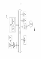
[0037] A este respeito, a Figura 4 ilustra uma seção transversal simplificada de um SOC 3DIC 110. O SOC 3DIC 110 tem múltiplos níveis 112. Os níveis 112 podem ser formados por corte de hidrogênio ou outro método de formação de níveis monolíticos. Para mais informações sobre um processo de corte de hidrogênio exemplar, o leitor interessado pode consultar o Pedido de Patente US número de série 13/765.080, depositado em 12 de Fevereiro de 2013, que é aqui incorporado por referência em sua totalidade.[0037] In this regard, Figure 4 illustrates a simplified cross-section of a
[0038] Como referido acima, o uso da tecnologia 3DIC permite que diferentes níveis das camadas 112 dentro do SOC 3DIC 110 realizem diferentes funções e forneçam todas as funções de um dispositivo em particular em um únic SOC 3DIC 110. Por exemplo, o SOC 3DIC 110 pode ser um transceptor de RF e um controlador para um terminal móvel, tal como um terminal móvel 10 acima descrito com referência à Figura 1. Deste modo, um primeiro nível 114 inclui sensores e outros elementos de tamanho grande.[0038] As noted above, the use of 3DIC technology allows different levels of
[0039] Ainda com referência à Figura 4, um segundo nível 116 pode incluir frequência de rádio, componentes analógicos e / ou de circuito integrado de gerenciamento de energia (PMIC), tal como o receptor 22, transmissor 24 e duplex / comutador 28. O segundo nível 116 pode ser projetado para ser relativamente de baixo ruído, de modo que sinais analógicos de RF de entrada não sejam distorcidos.[0039] Still referring to Figure 4, a
[0040] Com referência continuada à Figura 4, um protetor eletromagnético (EM) 118 pode ser posicionado entre o segundo nível 116 e um terceiro nível 120. O protetor EM 118 pode ser formado a partir de um material condutor, tal como uma camada de grafeno. Para mais informações sobre protetores de grafeno em 3DIC, o leitor interessado pode consultar o Pedido de Patente US número de série 13/765.061, depositado em 12 de Fevereiro de 2013, cuja divulgação é aqui incorporada por referência em sua totalidade.[0040] With continued reference to Figure 4, an electromagnetic shield (EM) 118 may be positioned between the
[0041] A presença do protetor EM 118 ajuda a evitar que o ruído dos primeiro e segundo níveis 114, 116 afete as características de baixo ruído do terceiro nível 120. O terceiro nível 120 pode ter um modem ou outro controlador. Para acomodar as funções sobre o terceiro nível 120, os materiais e o design do terceiro nível 120 podem ser selecionados para promover uma arquitetura de velocidade média.[0041] The presence of the
[0042] Com referência continuada à Figura 4, os quarto e quinto níveis 122, 124 podem ser uma montagem bitcell de memória com memória de acesso aleatório (RAM), incluindo RAM dinâmica (DRAM), RAM estática (SRAM) ou semelhante. Ambos os níveis 122, 124 podem ser concebidos para proporcionar circuitos de baixa fuga para melhorar o funcionamento da memória RAM.[0042] With continued reference to Figure 4, the fourth and
[0043] Com referência continuada à Figura 4, os sexto e sétimo níveis 126, 128 podem ser níveis de unidade de processamento geral. O sexto nível 126 pode incluir um processador de sinal digital (DSP), como o processador de banda de base 30 (Figura 1) usando uma combinação lógica, enquanto o sétimo nível 128 pode incluir um DSP que se baseia na lógica sequencial. Ambos os níveis 126, 128 podem ser concebidos para suportar altas velocidades em relação a problemas com fugas.[0043] With continued reference to Figure 4, the sixth and
[0044] Em uma forma de realização exemplar, os níveis são eletricamente interconectados por MIV 130. Para mais informações sobre MIV, o leitor interessado é direcionado a “High-Density Integration of Functional Modules Using Monolithic 3D-IC Technology” por Shreedpad Panth et al. nos anais da IEEE / ACM Asia South Pacific Design Automation Conference, 2013; pp. 681-686, que é aqui incorporada por referência em sua totalidade. Em contraste com TSV, MIV pode ser na ordem de sub 100 nm de diâmetro (isto é, muito menor do que as dimensões micrométricas da TSV) e 200 nm ou menos profundidade. Além disso, em uma forma de realização exemplar, cada um dos múltiplos níveis 112 pode ser de aproximadamente 400 nm de espessura ou menos. Estas dimensões são ilustradas na inserção da Figura 4.[0044] In an exemplary embodiment, the levels are electrically interconnected by
[0045] Ao fornecer diferentes níveis com diferentes funções e / ou ser capaz de dividir circuitos através de diferentes níveis, um sistema IC completo é possível, incluindo baterias, sensores, memória, funções de captação de energia, PMIC, processadores, componentes analógicos e digitais e similares. Cada nível pode ser optimizado para acomodar as funções posicionadas nele. Além disso, a densidade muito elevada de ligações nível a nível (isto é, o MIV) permite um elevado grau de integração a nível de wafer. O SOC 3DIC pode ter uma divisão 3D de nível celular homogêneo - montagens bitcell de memória de vários níveis, lógicas de combinação sequencial. Da mesma forma, o SOC 3DIC pode ter uma divisão 3D heterogênea de grão fino, como uma memória para núcleo digital, divisões lógicas de controle de montagem bitcell. Esta flexibilidade permite uma ampla gama de recursos de tecnologia para funções do sistema ideal.[0045] By providing different levels with different functions and/or being able to split circuits across different levels, a complete IC system is possible, including batteries, sensors, memory, power harvesting functions, PMIC, processors, analog components and digital and the like. Each level can be optimized to accommodate the functions placed on it. In addition, the very high density of layer-to-level links (ie the MIV) allows for a high degree of integration at the wafer level. SOC 3DIC can have a homogeneous cell-level 3D division - multi-level memory bitcell assemblies, sequential combination logics. Similarly, SOC 3DIC can have a fine-grained heterogeneous 3D division, such as a memory for digital core, bitcell assembly control logic divisions. This flexibility allows for a wide range of technology features for optimal system functions.
[0046] Como referido acima, em uma forma de realização exemplar, o SOC 3DIC pode ser um transceptor de RF completo e processador de banda de base em um único IC, tal como ilustrado na Figura 6. Em particular, a Figura 6 ilustra um terminal móvel 150 semelhante ao terminal móvel 10, com exceção que os elementos de circuito do terminal móvel 150 estão contidos dentro de um único 3DIC 152. A antena 16 e a interface de usuário 26 são distintas do 3DIC 152, embora seja possível incorporar uma antena em um 3DIC, se desejado. As funções dos elementos de circuito permanecem as mesmas e, portanto, são referenciadas com os mesmos números. Da mesma forma, um sistema de controle que tem um processador, bateria e memória pode estar em um único SOC 3DIC. Esse SOC 3DIC permite designs com economia de espaço, ao mesmo tempo permitindo desempenho superior do sistema porque os níveis individuais são adaptados às funções posicionados neles. O uso de protetores ou outras técnicas de isolamento permitem melhor isolamento do sinal. Além disso, há redução geral da complexidade na medida em que não são necessárias ligações com cabos externos entre diferentes camadas ou diferente IC. Em uma forma de realização exemplar, o SOC 3DIC total pode ser menos de 1 mm3.[0046] As noted above, in an exemplary embodiment, the 3DIC SOC may be a complete RF transceiver and baseband processor in a single IC, as illustrated in Figure 6. In particular, Figure 6 illustrates a
[0047] Com referência à Figura 7, um sistema com base em processador 154 semelhante ao sistema com base em processador 60 pode incluir um único 3DIC 156 que incorpora os elementos do circuito do sistema com base em processador. As funções dos elementos de circuito permanecer as mesmas e, portanto, são referidas com os mesmos números.[0047] Referring to Figure 7, a processor-based
[0048] Como mencionado acima, uma das outras vantagens de oferecer um 3DIC 110 com vários níveis 112 é que as características de funcionamento de um determinado nível podem ser adaptadas para uma necessidade ou desejo particular. Tais características de operação podem ser realizadas pelo uso de diferentes materiais (por exemplo, Si versus GaAs) ou pelo uso de diferentes tipos de máscaras para alterar os parâmetros como latência interna ou de fuga de corrente de memória. Um resumo exemplificativo de parâmetros ou características e como eles mudam o perfil operacional da memória é fornecido na Tabela 1 abaixo. Por exemplo, a(s) característica(s) de um transistor de transistores de célula de memória de parte(s) de uma memória pode ser modificada para compensar o aumento da latência interna para fuga de corrente reduzida. Neste sentido, a Tabela 1 abaixo ilustra várias características do transistor que podem ser modificadas para afetar a fuga de corrente e a latência interna da(s) parte(s) de memória. A Tabela 1 ilustra os efeitos da modificação do comprimento do canal de transistor de célula de memória (L), da largura do canal de transistor de célula de memória (W) e da tensão limite do transistor de célula de memória (Vt). Além disso, a Tabela 1 ilustra os efeitos da seleção entre transistores de célula de memória HVt, NVt ou LVt para fornecer a(s) parte(s) da memória. A Tabela 1 também ilustra os efeitos de polarização corpo do terminal do corpo (B) dos transistores de células de memória. A Tabela 1 ilustra vários efeitos da modificação das características acima mencionadas, incluindo: se a modificação aumenta (+) ou diminui (-) a condutância fonte-dreno (GDS) dos canais induzidos dos transistores de célula de memória da(s) parte(s) da memória; se a modificação aumenta (+) ou diminui (-) a resistência fonte-dreno (RDS) dos canais induzidos dos transistores de célula de memória da(s) parte(s) da memória; se a modificação aumenta (+) ou diminui (-) a fuga de corrente da(s) parte(s) da memória; e se a modificação aumenta (+) ou diminui (-) a latência interna da(s) parte(s) da memória. TABELA 1: EFEITOS EXEMPLARES DA MODIFICAÇÃO DAS CARACTERÍSTICAS DE TRANSISTORES DE CÉLULAS DE MEMÓRIA

[0049] Em uma forma de realização exemplar, um método de implementação de um 3DIC é ilustrado na Figura 5 pelo processo de 140. O processo inicia proporcionando uma pluralidade de níveis 112 (bloco 142). O processo continua fornecendo vários elementos funcionais através dos blocos 112 (bloco 144). O processo continua por interconexão dos níveis usando MIV 130 (bloco 146). Os vários níveis 112 e várias funções com a interconexão do MIV 130 formam, assim, um SOC 110 (bloco 148).[0049] In an exemplary embodiment, a method of implementing a 3DIC is illustrated in Figure 5 by
[0050] Também deve ser notado que as etapas operacionais descritas em qualquer uma das formas de realização exemplares aqui são descritas para proporcionar exemplos e discussão. As operações descritas podem ser realizadas em numerosas sequências diferentes, diferentes das sequências ilustradas. Além disso, as operações descritas em uma única etapa operacional podem, na verdade, ser realizadas em uma série de diferentes etapas. Além disso, uma ou mais etapas operacionais discutidas nas formas de realização exemplares podem ser combinadas. Deve ser entendido que as etapas operacionais ilustradas nos diagramas de fluxo podem ser sujeitas a numerosas modificações diferentes, como será prontamente aparente para um perito na arte. Os especialistas na técnica também entenderão que as informações e sinais podem ser representados utilizando qualquer de uma variedade de diferentes tecnologias e técnicas. Por exemplo, dados, instruções, comandos, informações, sinais, bits, símbolos, e chips que podem ser referenciados em toda a descrição acima podem ser representados por tensões, correntes, ondas eletromagnéticas, campos ou partículas magnéticas, campos ou partículas ópticas, ou qualquer combinação deles mesmos.[0050] It should also be noted that the operational steps described in any of the exemplary embodiments herein are described to provide examples and discussion. The described operations can be performed in numerous different sequences, different from the illustrated sequences. Furthermore, the operations described in a single operational step can actually be performed in a series of different steps. Furthermore, one or more operational steps discussed in the exemplary embodiments may be combined. It should be understood that the operational steps illustrated in the flow diagrams may be subject to numerous different modifications, as will be readily apparent to one skilled in the art. Those skilled in the art will also understand that information and signals can be represented using any of a variety of different technologies and techniques. For example, data, instructions, commands, information, signals, bits, symbols, and chips that may be referenced throughout the above description may be represented by voltages, currents, electromagnetic waves, magnetic fields or particles, optical fields or particles, or any combination of them.
[0051] A descrição anterior da invenção é fornecida para permitir que qualquer perito na arte possa fazer ou utilizar a invenção. Várias modificações à descrição serão prontamente aparentes para os peritos na arte, e os princípios genéricos definidos aqui poderão ser aplicados a outras variações sem afastamento do espírito ou âmbito da invenção. Assim, a descrição não se destina a ser limitada aos exemplos e desenhos aqui descritos, mas deve ser concedido o mais vasto âmbito consistente com os princípios e novas características aqui descritos.[0051] The foregoing description of the invention is provided to enable anyone skilled in the art to make or use the invention. Various modifications to the description will be readily apparent to those skilled in the art, and the general principles defined herein may apply to other variations without departing from the spirit or scope of the invention. Thus, the description is not intended to be limited to the examples and drawings described herein, but the widest scope consistent with the principles and novel features described herein should be granted.
Claims (13)
Applications Claiming Priority (5)
| Application Number | Priority Date | Filing Date | Title |
|---|---|---|---|
| US201361846648P | 2013-07-16 | 2013-07-16 | |
| US61/846,648 | 2013-07-16 | ||
| US14/013,399 US9418985B2 (en) | 2013-07-16 | 2013-08-29 | Complete system-on-chip (SOC) using monolithic three dimensional (3D) integrated circuit (IC) (3DIC) technology |
| US14/013,399 | 2013-08-29 | ||
| PCT/US2014/046503 WO2015009614A1 (en) | 2013-07-16 | 2014-07-14 | Complete system-on-chip (soc) using monolithic three dimensional (3d) integrated circuit (ic) (3dic) technology |
Publications (2)
| Publication Number | Publication Date |
|---|---|
| BR112016000868A2 BR112016000868A2 (en) | 2017-07-25 |
| BR112016000868B1 true BR112016000868B1 (en) | 2022-08-16 |
Family
ID=52343114
Family Applications (1)
| Application Number | Title | Priority Date | Filing Date |
|---|---|---|---|
| BR112016000868-5A BR112016000868B1 (en) | 2013-07-16 | 2014-07-14 | COMPLETE SYSTEM-ON-CHIP (SOC) USING THREE-DIMENSIONAL (3D) (3DIC) MONOLITHIC INTEGRATED CIRCUIT (IC) TECHNOLOGY |
Country Status (9)
| Country | Link |
|---|---|
| US (2) | US9418985B2 (en) |
| EP (1) | EP3022766A1 (en) |
| JP (1) | JP2016529702A (en) |
| KR (1) | KR101832330B1 (en) |
| CN (1) | CN105378918B (en) |
| BR (1) | BR112016000868B1 (en) |
| CA (1) | CA2917586C (en) |
| TW (1) | TWI618222B (en) |
| WO (1) | WO2015009614A1 (en) |
Families Citing this family (21)
| Publication number | Priority date | Publication date | Assignee | Title |
|---|---|---|---|---|
| US9418985B2 (en) | 2013-07-16 | 2016-08-16 | Qualcomm Incorporated | Complete system-on-chip (SOC) using monolithic three dimensional (3D) integrated circuit (IC) (3DIC) technology |
| EP2958028B1 (en) * | 2014-06-20 | 2020-05-13 | Nagravision S.A. | Physical interface module |
| US9256246B1 (en) * | 2015-01-29 | 2016-02-09 | Qualcomm Incorporated | Clock skew compensation with adaptive body biasing in three-dimensional (3D) integrated circuits (ICs) (3DICs) |
| US9628077B2 (en) | 2015-03-04 | 2017-04-18 | Qualcomm Incorporated | Dual power swing pipeline design with separation of combinational and sequential logics |
| CN105391823B (en) * | 2015-11-25 | 2019-02-12 | 上海新储集成电路有限公司 | A method of reducing mobile device size and power consumption |
| CN105742277B (en) * | 2016-04-13 | 2018-06-22 | 中国航天科技集团公司第九研究院第七七一研究所 | A kind of large-volume stereo integrates SRAM memory three-dimensional extended method |
| US9523760B1 (en) * | 2016-04-15 | 2016-12-20 | Cognitive Systems Corp. | Detecting motion based on repeated wireless transmissions |
| US9754923B1 (en) | 2016-05-09 | 2017-09-05 | Qualcomm Incorporated | Power gate placement techniques in three-dimensional (3D) integrated circuits (ICs) (3DICs) |
| US9929149B2 (en) | 2016-06-21 | 2018-03-27 | Arm Limited | Using inter-tier vias in integrated circuits |
| US9871020B1 (en) * | 2016-07-14 | 2018-01-16 | Globalfoundries Inc. | Through silicon via sharing in a 3D integrated circuit |
| US10678985B2 (en) * | 2016-08-31 | 2020-06-09 | Arm Limited | Method for generating three-dimensional integrated circuit design |
| US9712168B1 (en) * | 2016-09-14 | 2017-07-18 | Qualcomm Incorporated | Process variation power control in three-dimensional (3D) integrated circuits (ICs) (3DICs) |
| US10176147B2 (en) | 2017-03-07 | 2019-01-08 | Qualcomm Incorporated | Multi-processor core three-dimensional (3D) integrated circuits (ICs) (3DICs), and related methods |
| US10719100B2 (en) | 2017-11-21 | 2020-07-21 | Western Digital Technologies, Inc. | System and method for time stamp synchronization |
| US10727965B2 (en) * | 2017-11-21 | 2020-07-28 | Western Digital Technologies, Inc. | System and method for time stamp synchronization |
| CN110069795A (en) * | 2018-01-23 | 2019-07-30 | 长芯半导体有限公司 | Fast custom chip method |
| GB2586050B (en) * | 2019-07-31 | 2021-11-10 | Murata Manufacturing Co | Power supply output device |
| GB2586049B (en) * | 2019-07-31 | 2022-03-09 | Murata Manufacturing Co | Power supply output device |
| US11270917B2 (en) * | 2020-06-01 | 2022-03-08 | Alibaba Group Holding Limited | Scalable and flexible architectures for integrated circuit (IC) design and fabrication |
| EP4024222A1 (en) | 2021-01-04 | 2022-07-06 | Imec VZW | An integrated circuit with 3d partitioning |
| KR102443742B1 (en) * | 2021-02-08 | 2022-09-15 | 고려대학교 산학협력단 | A monolithic 3D based scratchpad memory |
Family Cites Families (34)
| Publication number | Priority date | Publication date | Assignee | Title |
|---|---|---|---|---|
| JPS61131474A (en) * | 1984-11-30 | 1986-06-19 | Agency Of Ind Science & Technol | Laminated semiconductor device |
| US6046078A (en) * | 1997-04-28 | 2000-04-04 | Megamos Corp. | Semiconductor device fabrication with reduced masking steps |
| US20030015768A1 (en) | 2001-07-23 | 2003-01-23 | Motorola, Inc. | Structure and method for microelectromechanical system (MEMS) devices integrated with other semiconductor structures |
| WO2003030252A2 (en) | 2001-09-28 | 2003-04-10 | Hrl Laboratories, Llc | Process for producing interconnects |
| US7126214B2 (en) * | 2001-12-05 | 2006-10-24 | Arbor Company Llp | Reconfigurable processor module comprising hybrid stacked integrated circuit die elements |
| JP2004165269A (en) * | 2002-11-11 | 2004-06-10 | Canon Inc | Laminated semiconductor device |
| KR100569590B1 (en) | 2003-12-30 | 2006-04-10 | 매그나칩 반도체 유한회사 | Radio frequency semiconductor device and method of manufacturing the same |
| DE102006030267B4 (en) * | 2006-06-30 | 2009-04-16 | Advanced Micro Devices, Inc., Sunnyvale | Nano embossing technique with increased flexibility in terms of adjustment and shaping of structural elements |
| US7692448B2 (en) | 2007-09-12 | 2010-04-06 | Neal Solomon | Reprogrammable three dimensional field programmable gate arrays |
| US8136071B2 (en) | 2007-09-12 | 2012-03-13 | Neal Solomon | Three dimensional integrated circuits and methods of fabrication |
| ATE512114T1 (en) * | 2008-09-03 | 2011-06-15 | St Microelectronics Tours Sas | THREE-DIMENSIONAL STRUCTURE WITH VERY HIGH DENSITY |
| US7986042B2 (en) * | 2009-04-14 | 2011-07-26 | Monolithic 3D Inc. | Method for fabrication of a semiconductor device and structure |
| US8115511B2 (en) * | 2009-04-14 | 2012-02-14 | Monolithic 3D Inc. | Method for fabrication of a semiconductor device and structure |
| US20110199116A1 (en) | 2010-02-16 | 2011-08-18 | NuPGA Corporation | Method for fabrication of a semiconductor device and structure |
| WO2010132715A2 (en) * | 2009-05-14 | 2010-11-18 | Sri International | Low cost high efficiency transparent organic electrodes for organic optoelectronic devices |
| TWI501380B (en) * | 2010-01-29 | 2015-09-21 | Nat Chip Implementation Ct Nat Applied Res Lab | Three-dimensional soc structure stacking by multiple chip modules |
| US8450779B2 (en) | 2010-03-08 | 2013-05-28 | International Business Machines Corporation | Graphene based three-dimensional integrated circuit device |
| JP2012019018A (en) * | 2010-07-07 | 2012-01-26 | Toshiba Corp | Semiconductor device and method of manufacturing the same |
| CN102024782B (en) * | 2010-10-12 | 2012-07-25 | 北京大学 | Three-dimensional vertical interconnecting structure and manufacturing method thereof |
| EP2469597A3 (en) | 2010-12-23 | 2016-06-29 | Commissariat à l'Énergie Atomique et aux Énergies Alternatives | Multi-level integrated circuit, device and method for modeling multi-level integrated circuits |
| TWI496271B (en) * | 2010-12-30 | 2015-08-11 | Ind Tech Res Inst | Wafer level molding structure and manufacturing method thereof |
| DE102011004581A1 (en) * | 2011-02-23 | 2012-08-23 | Globalfoundries Dresden Module One Limited Liability Company & Co. Kg | A technique for reducing plasma-induced etch damage during the fabrication of vias in inter-layer dielectrics by modified RF power ramp-up |
| US8975670B2 (en) | 2011-03-06 | 2015-03-10 | Monolithic 3D Inc. | Semiconductor device and structure for heat removal |
| JP6019599B2 (en) * | 2011-03-31 | 2016-11-02 | ソニー株式会社 | Semiconductor device and manufacturing method thereof |
| US8796741B2 (en) | 2011-10-04 | 2014-08-05 | Qualcomm Incorporated | Semiconductor device and methods of making semiconductor device using graphene |
| US9496255B2 (en) * | 2011-11-16 | 2016-11-15 | Qualcomm Incorporated | Stacked CMOS chipset having an insulating layer and a secondary layer and method of forming same |
| JP5981711B2 (en) * | 2011-12-16 | 2016-08-31 | ルネサスエレクトロニクス株式会社 | Semiconductor device and manufacturing method of semiconductor device |
| JP2013215917A (en) | 2012-04-05 | 2013-10-24 | Seiko Epson Corp | Printing apparatus and printing method |
| CN103545275B (en) * | 2012-07-12 | 2016-02-17 | 中芯国际集成电路制造(上海)有限公司 | Silicon through hole encapsulating structure and formation method |
| US8889491B2 (en) * | 2013-01-28 | 2014-11-18 | International Business Machines Corporation | Method of forming electronic fuse line with modified cap |
| US9171608B2 (en) * | 2013-03-15 | 2015-10-27 | Qualcomm Incorporated | Three-dimensional (3D) memory cell separation among 3D integrated circuit (IC) tiers, and related 3D integrated circuits (3DICS), 3DIC processor cores, and methods |
| KR20140113024A (en) * | 2013-03-15 | 2014-09-24 | 에스케이하이닉스 주식회사 | Resistance variable Memory Device And Method of Driving The Same |
| US9418985B2 (en) | 2013-07-16 | 2016-08-16 | Qualcomm Incorporated | Complete system-on-chip (SOC) using monolithic three dimensional (3D) integrated circuit (IC) (3DIC) technology |
| US9070711B2 (en) * | 2013-08-02 | 2015-06-30 | Globalfoundries Inc. | Methods of forming cap layers for semiconductor devices with self-aligned contact elements and the resulting devices |
-
2013
- 2013-08-29 US US14/013,399 patent/US9418985B2/en not_active Expired - Fee Related
-
2014
- 2014-06-30 TW TW103122569A patent/TWI618222B/en not_active IP Right Cessation
- 2014-07-14 JP JP2016527009A patent/JP2016529702A/en active Pending
- 2014-07-14 EP EP14747230.2A patent/EP3022766A1/en not_active Ceased
- 2014-07-14 KR KR1020167003723A patent/KR101832330B1/en active IP Right Grant
- 2014-07-14 WO PCT/US2014/046503 patent/WO2015009614A1/en active Application Filing
- 2014-07-14 BR BR112016000868-5A patent/BR112016000868B1/en active IP Right Grant
- 2014-07-14 CN CN201480039458.6A patent/CN105378918B/en active Active
- 2014-07-14 CA CA2917586A patent/CA2917586C/en active Active
-
2016
- 2016-08-09 US US15/231,836 patent/US9583473B2/en active Active
Also Published As
| Publication number | Publication date |
|---|---|
| CN105378918B (en) | 2018-05-04 |
| TW201513299A (en) | 2015-04-01 |
| US9583473B2 (en) | 2017-02-28 |
| TWI618222B (en) | 2018-03-11 |
| EP3022766A1 (en) | 2016-05-25 |
| KR101832330B1 (en) | 2018-02-26 |
| JP2016529702A (en) | 2016-09-23 |
| US20150022262A1 (en) | 2015-01-22 |
| CA2917586C (en) | 2019-02-12 |
| US9418985B2 (en) | 2016-08-16 |
| KR20160032182A (en) | 2016-03-23 |
| BR112016000868A2 (en) | 2017-07-25 |
| WO2015009614A1 (en) | 2015-01-22 |
| CN105378918A (en) | 2016-03-02 |
| US20160351553A1 (en) | 2016-12-01 |
| CA2917586A1 (en) | 2015-01-22 |
Similar Documents
| Publication | Publication Date | Title |
|---|---|---|
| BR112016000868B1 (en) | COMPLETE SYSTEM-ON-CHIP (SOC) USING THREE-DIMENSIONAL (3D) (3DIC) MONOLITHIC INTEGRATED CIRCUIT (IC) TECHNOLOGY | |
| US11296083B2 (en) | Three-dimensional (3D), vertically-integrated field-effect transistors (FETs) electrically coupled by integrated vertical FET-to-FET interconnects for complementary metal-oxide semiconductor (CMOS) cell circuits | |
| US11270991B1 (en) | Integrated circuits (ICs) employing front side (FS) back end-of-line (BEOL) (FS-BEOL) input/output (I/O) routing and back side (BS) BEOL (BS-BEOL) power routing for current flow organization, and related methods | |
| TW202133566A (en) | Impedance matching transceiver | |
| US10490558B2 (en) | Reducing or avoiding mechanical stress in static random access memory (SRAM) strap cells | |
| EP3060967B1 (en) | Monolithic three dimensional (3d) integrated circuits (ics) (3dics) with vertical memory components | |
| US10483200B1 (en) | Integrated circuits (ICs) employing additional output vertical interconnect access(es) (VIA(s)) coupled to a circuit output VIA to decrease circuit output resistance | |
| US11404374B2 (en) | Circuits employing a back side-front side connection structure for coupling back side routing to front side routing, and related complementary metal oxide semiconductor (CMOS) circuits and methods | |
| US11437335B2 (en) | Integrated circuit (IC) packages employing a thermal conductive package substrate with die region split, and related fabrication methods | |
| US9013235B2 (en) | Monolithic three dimensional (3D) flip-flops with minimal clock skew and related systems and methods | |
| US20210280684A1 (en) | Transistor with insulator | |
| US11295991B2 (en) | Complementary cell circuits employing isolation structures for defect reduction and related methods of fabrication | |
| US20230299044A1 (en) | Passive electrical components in mold metal layers of a multi-die complex | |
| TW202410471A (en) | Stacked complementary field effect transistor (cfet) and method of manufacture | |
| US20240021586A1 (en) | Stacked complementary field effect transistor (cfet) and method of manufacture | |
| US20230380067A1 (en) | Compressed pinouts for high-speed differential pairs | |
| CN116344538A (en) | Transistor with epitaxial source/drain liner for improved contact resistance |
Legal Events
| Date | Code | Title | Description |
|---|---|---|---|
| B06F | Objections, documents and/or translations needed after an examination request according [chapter 6.6 patent gazette] | ||
| B06U | Preliminary requirement: requests with searches performed by other patent offices: procedure suspended [chapter 6.21 patent gazette] | ||
| B350 | Update of information on the portal [chapter 15.35 patent gazette] | ||
| B07A | Application suspended after technical examination (opinion) [chapter 7.1 patent gazette] | ||
| B09A | Decision: intention to grant [chapter 9.1 patent gazette] | ||
| B16A | Patent or certificate of addition of invention granted [chapter 16.1 patent gazette] |
Free format text: PRAZO DE VALIDADE: 20 (VINTE) ANOS CONTADOS A PARTIR DE 14/07/2014, OBSERVADAS AS CONDICOES LEGAIS |