JP4266477B2 - Information processing apparatus and control method thereof - Google Patents
Information processing apparatus and control method thereof Download PDFInfo
- Publication number
- JP4266477B2 JP4266477B2 JP2000049688A JP2000049688A JP4266477B2 JP 4266477 B2 JP4266477 B2 JP 4266477B2 JP 2000049688 A JP2000049688 A JP 2000049688A JP 2000049688 A JP2000049688 A JP 2000049688A JP 4266477 B2 JP4266477 B2 JP 4266477B2
- Authority
- JP
- Japan
- Prior art keywords
- clock
- data
- signal
- fifo
- memory
- Prior art date
- Legal status (The legal status is an assumption and is not a legal conclusion. Google has not performed a legal analysis and makes no representation as to the accuracy of the status listed.)
- Expired - Fee Related
Links
Images


Classifications
-
- Y—GENERAL TAGGING OF NEW TECHNOLOGICAL DEVELOPMENTS; GENERAL TAGGING OF CROSS-SECTIONAL TECHNOLOGIES SPANNING OVER SEVERAL SECTIONS OF THE IPC; TECHNICAL SUBJECTS COVERED BY FORMER USPC CROSS-REFERENCE ART COLLECTIONS [XRACs] AND DIGESTS
- Y02—TECHNOLOGIES OR APPLICATIONS FOR MITIGATION OR ADAPTATION AGAINST CLIMATE CHANGE
- Y02D—CLIMATE CHANGE MITIGATION TECHNOLOGIES IN INFORMATION AND COMMUNICATION TECHNOLOGIES [ICT], I.E. INFORMATION AND COMMUNICATION TECHNOLOGIES AIMING AT THE REDUCTION OF THEIR OWN ENERGY USE
- Y02D30/00—Reducing energy consumption in communication networks
- Y02D30/70—Reducing energy consumption in communication networks in wireless communication networks
Description
【0001】
【発明の属する技術分野】
本発明は、例えばディジタル・スチルカメラや携帯テレビ電話端末装置、或はカメラ内蔵型ノートPC等に適用できる情報処理装置及びその方法に関するものである。
【0002】
【従来の技術】
近年、CCD等の固体撮像装置の小型化、省電力化及びLSIの高集積化、高機能化、低消費電力化などの技術の進展に伴い、ディジタルスチルカメラに代表されるように、電池で駆動可能な携帯型の撮影装置が一般に利用されるようになった。更には、携帯電話機能を内蔵した携帯型テレビ電話端末やカメラを内蔵したノート型PC等も開発されている。このような特に電池で駆動される撮影装置では、電池による動作時間を延長するために電力削減が求められている。また、AC電源で駆動される撮影装置においても、環境保全等の観点により、より有効な省電力機能が求められてきている。そのため従来から電池残量を常に表示し、残量が少なくなってきた場合は、ユーザに電源をこまめに切ることを促したり、ユーザの選んだ動作モードに応じて非動作部分のクロック供給を遮断したりする節電機能が実現されている。
【0003】
【発明が解決しようとする課題】
一般に撮影装置においては、撮影される画像のフレームレートと解像度が高くなるほど単位時間当たりに処理すべき画像データ量が増大するため、画像データを扱う電子回路は高い動作クロック周波数を必要とする。一般に、回路の消費電力は、その回路を駆動するクロック周波数に比例して増大するため、画像のフレームレートと解像度の増大は消費電力の増大をもたらす。従って、消費電力を低減するためには、極力フレームレートと解像度を小さくするほうが望ましい。
【0004】
しかしながら、例えばデジタルカメラなどの撮影装置では、その動作モードによって取り込む画像のフレームレートや解像度に対する要求が異なる。例えば、電子ビューファインダモード(EVFモードと呼ぶ)においては、極力スムーズな動画像が表示されることが望ましいが、その表示画面は機器に内蔵された小さな画面であることが多い。従って、フレームレートは大きい程良いが、解像度はそれほど要求されない。また静止画取り込みモード(撮影モードと呼ぶ)では、フレームレートは最低でよい(静止画のため)が、解像度は最大であることが要求される。更に記録した画像を再生する再生モードでは、撮像素子による画像信号の取り込みを行わず、表示部への表示が最大解像度で行われる。またテレビ電話モードでは、フレームレート、解像度ともに電話回線のデータ転送能力によって決定される。
【0005】
上記の例より明らかなように、このような撮影装置を構成する各々の機能ブロック、例えば撮影機能ブロック、画像処理機能ブロック、表示機能ブロックなどでは、その動作モードに応じて単位時間当たりに処理すべきデータ量が大幅に異なり、常に最大周波数で動作する必要がなく、正常な動作が行われる限り、できるだけ低い周波数で動作したほうが装置の消費電力を低減させることが可能になる。にもかかわらず、従来の技術では、完全に非動作状態にある機能ブロックへのクロック信号の供給を停止させるだけで、装置の消費電力を抑えるようにしていたため、有効な電力削減を行うことができなかった。
【0006】
本発明は上記従来例に鑑みてなされたもので、複数の処理手段のそれぞれに供給するクロック信号の周波数を、各処理手段が有するメモリに記憶されているデータ量の情報に応じて切り替えることにより、装置全体の消費電力を抑えることができる情報処理装置及びその制御方法を提供することを目的とする。
【0008】
【課題を解決するための手段】
上記目的を達成するために本発明の情報処理装置は以下のような構成を備える。即ち、
それぞれ周波数の異なる複数の周波数のクロック信号を発生するクロック発生源と、
前記クロック発生源から出力される複数の周波数のクロック信号のいずれかを選択する選択手段と、
それぞれが、処理済み或は処理対象のデータを記憶するメモリを有し、前記選択手段により選択されたクロック発生源からのクロック信号により動作する複数の処理手段と、
前記複数の処理手段の各処理手段が有する前記メモリに記憶されているデータ量の情報を取得し、当該取得したデータ量の情報に応じて各処理手段に対するクロック信号を選択するように制御する選択制御手段と、
を有することを特徴とする。
【0009】
上記目的を達成するために本発明の情報処理装置の制御方法は以下のような工程を備える。即ち、
それぞれが、処理済み或は処理対象のデータを記憶するメモリを有しクロック発生源からのクロック信号により動作する複数の処理手段を有する情報処理装置の制御方法であって、
前記複数の処理手段の各処理手段を動作させるために、それぞれ周波数の異なる複数の周波数のクロック信号を発生するクロック発生源から出力される複数の周波数のクロック信号のいずれかを選択する選択工程と、
前記複数の処理手段の各処理手段が有するメモリに記憶されているデータ量の情報を取得し、前記取得したデータ量の情報に応じて各処理手段に対するクロック信号を選択するように制御する選択制御工程と、
を有することを特徴とする。
【0010】
【発明の実施の形態】
以下、添付図面を参照して本発明の好適な実施の形態を詳細に説明する。
【0011】
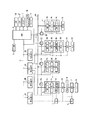
図1は、本発明の実施の形態に係る携帯型のテレビ電話端末装置の構成を示すブロック図である。図1において、各機能ブロック間を接続する線のうち、データ系の接続を太い実線で図示し、制御系の接続を細い実線で図示し、クロック系の接続を点線で図示している。但し、全ての接続が図示されているわけではなく、説明に必要な代表的な配線接続のみを図示した。
【0012】
このテレビ電話端末装置の主要なブロック構成として、撮像した画像信号の取り込みに関する処理を実行する画像取り込みコントローラ1、その画像信号から生成した画像データに対して画像処理を実行する信号処理プロセッサ2、画像データに基づく画像表示に関わる処理を行う表示コントローラ3、画像データをメモリに記憶させるためのメモリ制御を行うメモリコントローラ4、装置全体の制御を行うCPU5を有している。
【0013】
まず、代表的な動作モードとして、EVF(ビューファインダ)モード、撮影モード、再生モード及びテレビ電話モードのそれぞれについて動作を説明を行う。
【0014】
[画像取り込みコントローラ1の説明]
撮像対象の画像がレンズモジュール6を介してCCD7上に結像されることにより、その画像に応じた画像信号がCCD7から出力される。尚、このレンズモジュール6は、レンズ、オート・アイリスのための駆動系、オートフォーカスのための駆動系等を備えており、これら駆動系の制御は図示しない制御信号によってCPU5によって行われる。CCD7から出力される画像信号は前処理モジュール(CDS・AGC)8に入力される。本実施の形態においては、CCD7の取り込む有効画素数は640×480画素(VGA相当)である。前処理モジュール8は、CDS(相関二重サンプリング)及びAGC(自動利得制御)機能を備えている。また、CCD7及び前処理モジュール8に対するクロック及びタイミング信号は、タイミング生成回路(TG)9より供給される。前処理モジュール8で前処理が施された画像データは、A/D変換器(ADC)10により10ビットのディジタルデータに変換され、タイミング生成回路(SG)11により生成されるピクセルクロック(Pixel Clock)に同期して画像取り込みコントローラ1に入力される。
【0015】
画像取り込みコントローラ1に入力された画像データは間引き回路1aによって間引き処理され、間引かれた結果であるデータがFIFO1bに書き込まれる。この間引き回路1aにおける間引き方式は、図示しない制御信号によってCPU5によって予め設定されている。
【0016】
図2(A)は、間引き回路1aの動作の一例を示すタイミングチャートである。間引き回路1aは、SG11から入力されるピクセルクロック(Pixel Clock)を計数するピクセルカウンタ(Pixel Count)、図示しない水平・垂直同期信号に基づいて、画像のライン数を計数するラインカウンタ(Line Num)を備えており、CPU5によって予め設定された間引き方式と、これらのカウンタの計数値に基づいて、ADC10から入力されるデジタル画像データをラッチし、FIFO1bに書き込むためのクロック(Latch Clock)を生成する。
【0017】
図2(A)の例では、水平640ピクセル、垂直480ラインのデータに対し水平・垂直とも1/2の間引きを行う場合(320×240画素:CIF相当)が例示されている。従って、有効ラインは奇数ラインであり、この期間を示すための信号がActive Line信号である。また、有効ピクセルは奇数ピクセルであり、これを示す信号がActive Pixel信号である。
【0018】
これら信号を基に、図2(B)に示すようにPixel Clock、Active Line信号及びActive Pixel信号の論理積が取られ、これがFIFO1bに書き込むためのLatch Clock信号となる。なお、図2(A)において、FIFO1bに書き込まれるデータがData to FIFOである。
【0019】
尚、この間引き回路1aは、フレーム間引き機能も備える構成にすることが可能である。この場合は、更にフレームカウンタを設け、例えば4フレームごとに1フレームを取り込む場合にはフレームカウンタが「4の倍数+1」のときにActive Frame信号を生成し、図2(B)に示すAND回路の入力に加えるようにすればよい。
【0020】
バスインターフェース回路(BUS IF)1cは、FIFO1bが空でない状態(何等のデータが書込まれている)を検知すると、メインバス(MB)上にデータ書き込みのバストランザクションを発生し、メモリコントローラ4にFIFO1bから読み出したデータを転送する。バスインターフェース回路1cは、通常、画像取り込みクロック(Latch Clock)とは非同期のバスクロックで動作している。従って、FIFO1bの読み出しクロックは、FIFO1bの書き込みクロック(Latch Clock)とは非同期であり、FIFO1bはこの非同期のデータ転送を緩衝するために備えられている。
【0021】
尚、このメインバスMBには、他にもバストランザクションを発生するバスマスタが複数接続されている(信号処理プロセッサ2、表示コントローラ3、CPU5など)ので、同時に複数のバストランザクションが発生する可能性がある。そのためバスアービタ12は、1度に1つだけのバスマスタがバストランザクションを発生できるようにバスを調停する。
【0022】
[メモリコントローラ4の説明]
メモリコントローラ4は、バスインターフェース回路(BUS IF)4aにおいてバストランザクションを受信し、格納すべき画像データ及びその画像データを格納すべきメモリアドレスを一時バッファ4bに書き込む。SDRAMインターフェース回路(SDRAM IF)4cは、画像メモリであるSDRAM13への各種制御信号を出力するとともに、バッファ4bに格納されたメモリアドレス及び画像データをSDRAM13に出力する。バスインターフェース回路4a、バッファ4b、SDRAMインターフェース回路4c、及びSDRAM13は全てバスクロックに同期して動作する。
【0023】
[信号処理プロセッサ2の説明]
信号処理プロセッサ2は、画像データの読み出しのためのバストランザクションを発生し、バスクロックで動作するバスインターフェース回路(BUS IF)2aによって、画像取り込みコントローラによって取り込まれた画像データを画像メモリから読み出す。こうして読み出された画像データはバスクロックに同期して双方向FIFO2bに書き込まれる。DSP(デジタル信号プロセッサ)2cは、バスクロックとは異なるクロック(DSPクロック)で動作しており、このDSPクロックに同期して双方向FIFO2bのデータにアクセスして、カラーマトリクス処理によりYC分離を行い、続いて色補正、エッジ強調、ホワイトバランス調整、ガンマ補正などの処理を行う。このようにして得られた画像データは、モニタ15への表示に用いられる他、画像圧縮にも用いられる。モニタ15への表示用に用いる場合は、表示コントローラ3が読み出せるように、バスインターフェース回路2aを起動して、書き込みのバストランザクションを発生し、SDRAM13にデータを転送する。
【0024】
[EVFモードの説明]
EVFモードにおいては、上述した動作をフレーム毎に繰り返すことによって、連続したフレームを画像メモリ13に取り込む。信号処理プロセッサ2が画像データを書込む画像メモリの領域としては、同一領域を上書きする動作でよい。表示コントローラ3は、その画像メモリの領域より画像データを読み出すことにより表示データを得る。その際、表示コントローラ3は、画像データを読み出すためのバストランザクションを発生し、バスクロックで動作するバスインターフェース回路(BUS IF)3aによって画像メモリ13から表示すべき画像データを読み出す。表示コントローラ3は更に、この読み出した画像データをバスクロックに同期してFIFO3bの書き込みポートに入力する。NTSCのモニタや液晶ディスプレイに代表されるように、一般に表示装置は画面を絶え間なくリフレッシュする必要があるため、有効画面期間中は、あるピクセルクロックで動作し続けなければならない。そのためバスインターフェース回路3aは、FIFO3bがフル状態になるまで画像メモリから画像データを読み出し続ける。
【0025】
次に補間回路3cは、表示ピクセルクロックに同期してFIFO3bより画像データを読み出す。補間回路3cはラインメモリを備えており、FIFO3bより読み出された画像データは、まずこのラインメモリに格納される。このラインメモリに格納された画像データは、補間なしの場合は先頭から順に読み出されてNTSCエンコーダ3dに入力され、NTSCフォーマットの映像データに変換される。この場合、補間回路3cは、1ピクセル分の画像データが読み出されると、直ちに1ピクセル分の画像データをFIFO3bから読み出す。ここでライン補間を行う場合は、(補間するライン数−1)分のラインデータをNTSCエンコーダ3dに送出した後、次のラインは1ピクセル分の画像データをNTSCエンコーダ3dに送出する毎に、FIFO3bから1ピクセル分の画像データを読み出す。例えば、ここでライン方向に4倍の補間を施すときは、3ライン分をそのラインメモリからの画像データで表示し、4ライン目の表示の際には、そのラインの表示を行いながらFIFO3bから次のラインの画像データを読み込んでくるという動作を行う。
【0026】
NTSCエンコーダ3dによってNTSCフォーマットに変換された映像データは、D/A変換器(DAC)14によってアナログ信号に変換された後、NTSCのモニタ15によって表示される。
【0027】
上記の動作をフレームごとに連続して行うことにより、EVFモードの動作となる。このEVFモードでは、画像取り込みコントローラ1がフレーム間引きを行っていたとしても、各フレーム分の画像データを読み出す必要がある。この場合、表示される画像はこま落しになるが、モニタ15は一定のフレームレートで動作し続ける必要があるからである。
【0028】
[撮影モードの説明]
次に、撮影モードでの動作を説明する。この撮影モードでは、1フレーム分の画像データを取り込んだ後、この画像データをJPEG圧縮してメモリカード17などの外部記憶等に記録する。
【0029】
まず、シャッタ・ボタン等含むスイッチ群16のシャッタ・ボタンの押下がCPU5によって検出されると、CPU5は図示しない制御信号により画像取り込みコントローラ1に対し、次の1フレームの画像データを取り込み、それ以降のフレームの画像データを取り込まないように指示する。同様に、信号処理プロセッサ2に対し、次の1フレームの画像データに対して圧縮処理を行うように通知する。
【0030】
画像取り込みコントローラ1は、前述のEVFモードの場合とは異なり、1フレームの画像を取り込んで画像メモリ13に画像データを転送し終えると、動作を一時停止する。信号処理プロセッサ2は、このメモリ13に格納された1フレーム分の画像データを読み出して、EVFモードで表示用の画像データを生成した場合と全く同様にしてYC分離、色補正、エッジ強調、ホワイトバランス調整、ガンマ補正等の画像処理を行う。その後、直ちにその画像データに対して、DCT演算処理、量子化処理、可変長符号化処理などを施して得られた符号化データを、画像メモリ13内の表示用画像データ領域とは別の領域に書き込む。
【0031】
CPU5は、画像メモリ13に記憶された画像データを読み出し、必要なマーカ等を付加してJPEGデータとした後に、メモリカード17に格納する。こうして1フレーム分の画像データの格納が終了すると、CPU5は画像取り込みコントローラ1に対して、EVFモードでの画像信号の取り込み再開するように通知する。
【0032】
なお、メモリカード17に格納された符号化された画像データは、PC等のホストコンピュータとのインターフェースを実現するコミュニケーション回路18を介して、PC等からアクセスすることが可能である。本実施の形態においてはコミュニケーション回路18は、例えばシリアルインターフェース、USB、IrDA、携帯電話モジュールなどを含んでいる。
【0033】
[再生モードの説明]
次に再生モードの動作を説明する。この再生モードでは、画像取り込みコントローラ1の動作は停止している。CPU5はメモリカード17に格納された符号化された圧縮データを読み出してSDRAM13に書き込む。信号処理プロセッサ2は、このSDRAM13に書込まれた符号データを読み出して、復号化、逆量子化、逆DCT変換等の画像伸長処理を行って表示可能な画像データとした後、再びSDRAM13に書き戻す。表示コントローラ3は、この表示可能データをSDRAM13より読み出して表示動作を行う。
【0034】
[テレビ電話モードの説明]
次に、テレビ電話モードの動作を説明する。前述した撮影モードでは、1フレームの画像データを取り込んだ後、画像取り込みコントローラ1は一時動作を停止した。しかし、このテレビ電話モードでは、画像データの取り込み処理を中断せずに、次々に連続するフレームの画像データを取り込む。このときの取り込みフレームレートは、CPU5によって設定された間引き方式に基づいて決定される。こうして取り込まれた画像データは撮影モードの場合と同様の処理によって信号処理プロセッサ2により画像処理及び画像圧縮・符号化処理が施されて、SDRAM13に書き込まれる。こうしてSDRAM13に書き込まれた符号データは、CPU5により読み出され、所定のマーカ等が挿入された後、コミュニケーション回路18の携帯電話モジュールによって電話回線を通じて通話相手に伝送される。
【0035】
一方、電話回線を通じて通話相手より受信した符号データは、コミュニケーション回路18からCPU5を経由してSDRAM13に書き込まれる。信号処理プロセッサ2は、このSDRAM13に書込まれた符号データを読み出して、復号化、逆量子化、逆DCT変換等の画像伸長処理を行って表示可能な画像データとした後、再びSDRAM13に書き戻す。表示コントローラ3は、表示すべき画像データをSDRAM13より読み出してモニタ15に表示するように表示動作を行う。
【0036】
以上のようにして、CCD7により撮像した画像を通話相手に電送するとともに、通信相手から送られてくる画像データを受信してモニタ15に表示することができる。
【0037】
[クロックの説明]
次に、画像取り込みコントローラ1、信号処理プロセッサ2、表示コントローラ3及びメモリコントローラ4のそれぞれに供給されるクロックについて説明する。
【0038】
クロック発生器(CG)19,20,21,22は、CPU5により、そのクロック出力をオン/オフできる可変クロック発生器である。クロック発生器(CG(C))19は、SG11及び画像取り込みコントローラ1の画像取り込み部(間引き回路1a、FIFO1b)の動作クロックを生成する。クロック発生器(CG(D))20は、DSP2cの動作クロックを生成する。クロック発生器(CG(B))21は、各コントローラのバスインターフェース部の動作クロックを生成する。クロック発生器(CG(N))22は、表示コントローラ3のFIFO3b、補間回路3c、NTSCエンコーダ3d及びD/A変換器14の動作クロックを生成する。
【0039】
またクロック発生器21から出力されるバスクロックは、各コントローラのバスインターフェース回路に供給されるが、各コントローラ毎にクロック供給を停止できるようにクロックゲート回路(G)23,24,25,26を備えている。この内、クロックゲート回路26はCPU5によって制御され、クロックゲート回路23はFIFO1bからの制御信号により制御され、クロックゲート回路24はFIFO2bからの、クロックゲート回路25はFIFO3bからの制御信号により制御される。
【0040】
次に、動作モードに応じて間引き回路1a、補間回路3cの設定をどのように制御するかを説明する。
【0041】
動作モードの変更は、ユーザによるスイッチ群16の操作によって行われる。スイッチの構成は様々な例が考えられるが、本実施の形態ではダイアルと押しボタンにより構成する。ダイアルの回転により動作モードの候補が順次更新されて表示され、その候補が表示されている時に押しボタンの押下により、その表示されている動作モードが実際の動作モードとして選択される。この動作モードの選択のイベントによりCPU5に割り込みが発生し、ROM27に格納された割り込み処理ルーチンにより、動作モードの変更処理ルーチンが実行される。
【0042】
この動作モード変更処理ルーチンでは、新たに選択された動作モードを読み取り、その読み取られた動作モードに対応して間引き回路1a及び補間回路3cに初期値が設定される。これら間引き回路1a及び補間回路3cに設定されるデフォルト値は、工場出荷時のROM27に格納されている。ユーザが設定値を変更した場合は、その変更したことを示すフラグと共に、その変更を加えた部分の対応がRAM28に記録される。
【0043】
図3は、動作モードと間引き方式及び補間方式の設定値の対応例を説明する図である。
【0044】
ここでは動作モードとして、EVF、撮影、再生、テレビ電話の4種類が定義されている。間引き方式は解像度(図中ではサイズ(size)と表記)とフレームレート(図中ではフレーム(frame)と表記)とに分けて示しており、補間方式は解像度のみを示してある。なぜなら本実施の形態では、表示がNTSC出力であるためフレームレートが一定だからである。解像度の間引き・補間方式は縦横1/2間引き・補間の場合を「CIF」として示し、縦横1/4間引き・補間の場合を「QCIF」として示している。またフレームレートは、1秒間に30フレームならば30フレーム/s(frame/s)のように示している。また、停止状態を示す場合は「−」と図示している。
【0045】
図3に示す例によれば、動作モード変更ルーチンが読み取った新たな動作モードがEVFモードだった場合は、解像度の間引き・補間方式は「CIF」であり、フレームレートは30フレーム/sと設定する。また撮影モードでは、表示は停止しており、画像取り込みとしてはVGAを1フレームだけ取り込むように設定する。更に再生モードの場合は、画像取り込みは停止しており、表示としては「VGA」を表示する。またテレビ電話モードの場合は、解像度の間引き・補間方式は「QCIF」であり、フレームレートは15フレーム/sと設定する。CPU5は、この図3の内容に相当するデータをROM27又はRAM28より読み出して間引き回路1aにおける間引き方式、及び補間回路3cにおける補間方式の設定を得る。
【0046】
次にクロック発生器19〜22及びクロックゲート回路23〜26の設定をどのように制御するかを説明する。
【0047】
クロック発生器19は、CPU5からのオン信号によりピクセルクロックとして13.5MHzのクロック信号を出力する。このピクセルクロックは通常オン(出力される)であるが、再生モードの場合は新たに画像信号を取り込む必要はないためオフとされる。
【0048】
クロック発生器20は、CPU5からの2ビットのクロック選択信号により4種類の周波数のクロックを発生することができる。即ち、選択信号が“00”の場合は0MHz、即ちクロックの発生が停止された状態であり、“01”の場合は50MHzのクロックを出力し、“10”の場合は100MHzのクロックを出力し、“11”の場合には150MHzのクロックを出力する。この2ビットの選択信号は、ROM27に格納されてCPU5により読み出されて実行される制御プログラムによって制御される。即ち、動作モードと処理する画像データの解像度により単位時間に処理すべき画像データの量が異なるため、例えばEVFモードではVGAの場合は100MHzで動作させ、CIF及びQCIFでは50MHzで動作させるが、テレビ電話モードではVGAの場合は150MHzで動作させ、CIFの場合は100MHzで動作させ、QCIFの場合は50MHzで動作させる、というような制御を行う。
【0049】
クロック発生器21は、CPU5からのオン/オフ信号により起動/停止するとともに、起動状態にあってもFIFO1b,2b,3bからの制御信号によって、その発生するクロックの周波数が変更される。
【0050】
図4は、クロック発生器21の一例を示すブロック図である。
【0051】
21aはクロック原発振器で、80MHzのクロックを常時発生している。21bはクロックの1/2分周器であり、80MHzのクロック信号が入力され40MHzのクロック信号を出力する。21cはクロックの1/2分周器であり、40MHzのクロック信号が入力されて20MHzのクロック信号を出力する。21dはクロックの1/2分周器であり、20MHzのクロック信号が入力されて10MHzのクロック信号を出力する。21eはクロックセレクタで、4つのクロック入力A,B,C,Dのうち1つのクロックを選択信号SelA,SelB,SelC,SelDに応じて出力端子Outに出力する。
【0052】
図5は、このクロックセレクタ21eにおけるクロック信号の選択処理を説明する図である。
【0053】
選択信号SelA、SelB,SelC,SelDの順にプライオリティが高くなり、例えばSelDが“1”の場合は、他の選択信号の状態に拘わらずD端子に入力されたクロック信号がOut端子に出力される。ここで入力A,B,C,Dのそれぞれには、前述した周波数10MHz,20MHz,40MHz,80MHzのクロック信号がそれぞれ入力されている。また、端子SelAにはAND回路21fの出力が、端子SelBにはOR21gの出力が、端子SelCにはOR21hの出力が、そして端子SelDにはOR21Iの出力がそれぞれ接続されている。またAND21f,OR21g,21h,21iの各入力には、FIFO1b,2b,3bのポインタステータス信号がそれぞれ接続される。各々のポインタステータス信号の意味するところを、FIFO1bの一例の構成図である図6、FIFO2bの一例の構成図である図7、FIFO3bの一例の構成図である図8を用いて説明する。
【0054】
図6は、本実施の形態のFIFO1bの構成例を示すブロック図である。
【0055】
このFIFO1bは、同期型デュアルポートSRAM1b0、書き込み制御回路1b1、書き込みアドレス生成(ポインタ生成)回路1b2、読み出し制御回路1b3、読み出しアドレス生成(ポインタ生成)画路1b4及びポインタステータス生成回路1b5を備えている。
【0056】
デュアルポートSRAM1b0は、例えば128(ワード)×8(ビット)のデュアルポートSRAMで、間引き回路1aよりの書き込み有効信号(write en)が入力されるとCCDのピクセルクロック(ccd clk)に同期してCCDデータであるWRITE DATAが、書き込みアドレス生成(ポインタ生成)回路1b2から出力されるメモリアドレスに書き込まれる。こうしてデュアルポートSRAM1b0に1つの画像データが書き込まれた後、書込むアドレス生成回路1b2から出力される書き込みアドレスは1だけインクリメントされる。また読み出し動作は、バスインターフェース回路1cからの読み出し有効信号(read en)が入力されるとバスクロック(bus clk)に同期して読み出しアドレス生成(ポインタ生成)回路1b4の生成するポインタの示すアドレスからREAD DATAが出力される。
【0057】
こうして1つの画像データが読み出された後、読出しアドレス生成回路1b4から出力される読み出しアドレスは1だけインクリメントされる。ポインタステータス回路1b5は、書き込みポインタ(アドレス)と読み出しポインタ(アドレス)の差の絶対値を演算することにより、FIFO1bのステータスを出力する。例えば、差の絶対値が“0”の場合は、FIFO1bが空であることを示すので「1b:Empty」信号を出力する。また、この差の絶対値がFIFO1bの容量(128ワード)の80%以上の場合は、FIFO1bの有効データがFIFO1bの容量の20%以下であることを示すので「1b<20%」信号を出力する。同様に、FIFO1bの有効データが20%から40%の間の場合は「1b>20%」信号を出力し、40%から60%の間の場合は「1b>40%」信号を出力し、60%以上の場合は「1b>60%」信号を出力する。
【0058】
図7は、FIFO2bの構成を示すブロック図である。
【0059】
このFIFO2bは、バスインターフェース回路2aからDSP2c方向のFIFOと逆向きのFIFOの組み合わせとして実現される。バスインターフェース回路2aからDSP2c方向のFIFOは、同期型デュアルポートSRAM2b0、書き込み制御回路2b1、書き込みアドレス生成(ポインタ生成)回路2b2、読み出し制御回路2b3、読み出しアドレス生成(ポインタ生成)回路2b4及びポインタステータス生成回路2b5を備えている。
【0060】
一方、DSP2cからバスインターフェース回路2a向きのFIFOは、同期型デュアルポートSRAM2b6、書き込みアドレス生成(ポインタ生成)回路2b7、読み出しアドレス生成(ポインタ生成)回路2b8、書き込み制御回路2b9、読み出し制御回路2b10及びポインタステータス生成回路2b11を備えている。
【0061】
デュアルポートSRAM2b0は、例えば128(ワード)×8(ビット)のデュアルポートSRAMであり、バスインターフェース回路2aよりの書き込み有効信号(write en)が入力されるとバスクロック(bus clk)に同期してバス転送データであるWRITE DATAが書き込みアドレス生成(ポインタ生成)回路2b2の生成するメモリアドレスに書き込まれる。このデータの書き込み後、書き込みアドレス生成回路2b2から出力される書き込みポインタ(アドレス)はインクリメントされる。また読み出し動作は、DSP2cからの読み出し有効信号(read en)が入力されるとDSPクロック(dsp clk)に同期して読み出しアドレス生成(ポインタ生成)回路2b4の生成するポインタの示すアドレスからREAD DATAが出力されるので、これを読み出す。このデータの読み出し後、読み出しアドレス生成回路2b4から出力される読み出しポインタはインクリメントされる。ポインタステータス回路2b5は、これら書き込みポインタと読み出しポインタの差の絶対値を演算することにより、FIFO2bのステータスデータを出力する。
【0062】
またデュアルポートSRAM2b6は、例えば128(ワード)×8(ビット)のデュアルポートSRAMで、DSP2cからの書き込み有効信号(write en)が入力されるとDSPクロック(dsp clk)に同期してバス転送データであるWRITE DATAが書き込みアドレス生成(ポインタ生成)回路2b7の生成するメモリアドレスに書き込まれる。このデータ書き込み後、書き込みアドレス生成回路2b7から出力される書き込みポインタはインクリメントされる。また読み出し動作は、バスインターフェース回路2aからの読み出し有効信号(read en)が入力されるとバスクロック(bus clk)に同期して読み出しアドレス生成(ポインタ生成)回路2b8の生成するポインタの示すメモリアドレスからREAD DATAを出力するので、これを読み出す。このデータの読み出し後、読み出しアドレス生成回路2b8から出力される読み出しポインタがインクリメントされる。ポインタステータス回路2b11は、これら書き込みポインタと読み出しポインタの差の絶対値を演算することにより、FIFO2bのステータスを出力する。
【0063】
FIFO2bのポインタステータス信号は、上記ポインタステータス回路2b5,2b11の出力の演算により生成される。例えば、2つのFIFOポインタの差の絶対値がともに“0”の場合はFIFO2bが空であることを示すのでAND2b12により「2b:Empty」信号を出力する。2つのFIFOポインタの差の絶対値がともにFIFO2bの容量(128ワード)の80%以上の場合はFIFO2bの有効データがFIFO2bの容量の20%以下であることを示すので、AND2b13により「2b<20%」信号を出力する。同様に、少なくとも一方のFIFOの有効データが20%から40%の間の場合は、OR2b14により「2b>20%」信号を出力し、少なくとも一方が40%から60%の間の場合はOR2b15により「2b>40%」信号を出力し、更に少なくとも一方が60%以上の場合は、OR2b16により「2b>60%」信号を出力する。
【0064】
図8は、FIFO3bの構成を示すブロック図である。
【0065】
図8に示すように、FIFO3bは同期型デュアルポートSRAM3b0、書き込み制御回路3b1、書き込みアドレス生成(ポインタ生成)回路3b2、読み出し制御回路3b3、読み出しアドレス生成(ポインタ生成)回路3b4及びポインタステータス生成回路3b5を備えている。
【0066】
ここで3b0は、例えば128(ワード)×8(ビット)のデュアルポートSRAMであり、バスインターフェース回路3aよりの書き込み有効信号(write en)が入力されるとバスクロック(bus clk)に同期してバス転送データであるWRITE DATAが書き込みアドレス生成(ポインタ生成)回路3b2の生成するメモリアドレスに書き込まれる。このデータ書き込み後、書き込みアドレス生成回路3b2から出力される書き込みポインタがインクリメントされる。また読み出し動作は、補間回路3cからの読み出し有効信号(read en)が入力されると表示クロック(disp clk)に同期して読み出しアドレス生成(ポインタ生成)回路3b4の生成するポインタの示すメモリアドレスからREAD DATAを出力するのでこれを読み出す。このデータの読み出し後、読み出しアドレス生成回路3b4から出力される読み出しポインタがインクリメントされる。ポインタステータス回路3b5は、これら書き込みポインタと読み出しポインタの差の絶対値を演算することにより、FIFO3bのステータスを出力する。例えば、差の絶対値が“128”の場合はFIFO3bが一杯であることを示すので「3b:full」信号を出力し、差の絶対値がFIFO3bの容量(128ワード)の20%以下の場合は、FIFO3bの有効データがFIFO容量の80%以上であることを示すので「3b>80%」信号を出力する。同様に、FIFO3bの有効データが80%から60%の間の場合は「3b<80%」信号を出力し、60%から40%の間の場合は「3b<60%」信号を出力し、40%以下の場合は「3b<40%」信号を出力する。
【0067】
再び図4を用いてクロック発生器21の動作を説明する。
【0068】
各FIFOより入力されるポインタステータス信号は、AND21f,OR21g,21h,21iに入力される。ここでFIFO1b,2bはFIFO内の有効データが少ないほどバスの転送能力に余裕があることを示している。
【0069】
一方、FIFO3bは空き容量がある限りデータを先読みするため、FIFO3bがFULLに近いほどバスの転送能力に余裕があることを示す。AND21fには、「1b<20%」信号と「2b<20%」信号と「3b>80%」信号が入力されており、全ての入力が“1”である状態は全てのバスマスタにとってバス転送能力が十分あることを示している。従って、クロックの周波数を最低に設定することができるので、AND2fの出力をSelA入力とし、周波数10MHzのクロック信号が選択されるようにする。
【0070】
次に転送すべきデータ量が増加してFIFO1b又はFIFO2bの少なくとも一方が20%を超えるか、或はFIFO3bが80%を下回った場合は、OR21gの出力が“1”となり、周波数20MHzのクロック信号が選択される。更に転送すべきデータ量が増加してFIFO1b又はFIFO2bの少なくとも一方が40%を超えるか、或はFIFO3bが60%を下回った場合、OR21bの出力が“1”となり、周波数40MHzのクロック信号が選択される。更に転送すべきデータ量が増加してFIFO1b又はFIFO2bの少なくとも一方が60%を超えるか、或はFIFO3bが40%を下回った場合、OR21iの出力が“1”となり、周波数80MHzのクロック信号が選択される。即ち、少なくとも1つのバスマスタのデータ転送能力が不足してきたことを動的に検知してバスクロックの周波数を自動的に高くすることができる。なお、クロック発生器21のバスクロックを停止するためには、CPU5によってクロックオン信号を“0”に設定する。こうすることによりANDゲート21jによってセレクタ21eで選択されたバスクロックがゲートされ、クロック信号の出力が停止される。
【0071】
一方、クロック発生器22は、CPU5からのオン信号によりピクセルクロックとして周波数13.5MHzのクロック信号を出力する。
【0072】
次に、クロックゲート回路23,24,25の動作をクロックゲート回路の一例の構成図を用いて説明する。
【0073】
図9は、クロックゲート回路23を説明する回路図である。
【0074】
図9に示すように、クロックゲート回路23は、バスクロック(bus clk)をFIFO1bのエンプティ信号である「1b:Empty」信号(図6)の反転信号でゲートする。即ち、画像取り込みコントローラ1の取り込みデータがなくなると自動的に画像取り込みコントローラ1のバスインターフェース回路1aの動作クロック及びFIFO1bの読み出しクロックが停止する。
【0075】
図10は、クロックゲート回路24を説明する回路図である。
【0076】
図10に示すように、クロックゲート回路24は、バスクロック(bus clk)をFIFO2bのエンプティ信号である「2b:Empty」信号(図7)の反転信号でゲートする。即ち、信号処理プロセッサ2の処理データがなくなると自動的に信号処理プロセッサ2のバスインターフェース回路2aの動作クロック及びFIFO2bのバス側クロックが停止する。
【0077】
図11は、クロックゲート回路25を説明する回路図である。
【0078】
図11に示すように、クロックゲート回路25は、バスクロック(bus clk)をFIFO3bのフル信号である「3b:full」信号(図8)の反転信号でゲートする。即ち、表示コントローラ3の表示データをそれ以上読み出せない状態になると自動的に表示コントローラ2のバスインターフェース回路3aの動作クロック及びFIFO3bの書き込みクロックが停止する。
【0079】
フレームレートに対応するクロック発生器19〜22及びクロックゲート回路23〜26の設定は、CPU5によってフレームごとにクロック発生器及びクロックゲート回路を制御することによって行う。例えば、EVFモードにおいてフレームレートが10フレーム/sと設定されていたならば、画像取り込みコントローラ1及び信号処理プロセッサ2は、3フレームにつき1フレームだけ処理を行えばよいので、取り込みを行わない3フレーム中2フレーム分の期間はクロックゲート回路23及び24及びクロック発生器20により、画像取り込みコントローラ1及び信号処理プロセッサ2へのクロック信号の供給を停止させる。
【0080】
本実施の形態に示したような間引き方式、補間方式の設定とクロック周波数の制御によれば、あらゆる動作モードにおいてユーザの望む解像度やフレームレートを柔軟に設定できるとともに、ユーザの設定した解像度やフレームレートで正常に動作するためのクロック周波数が自動的に設定されるので、あらゆる動作状況においても最大限の省電力効果が得られる。
【0081】
なお本発明は、複数の機器(例えばホストコンピュータ、インターフェース機器、リーダ、プリンタなど)から構成されるシステムに適用しても、一つの機器からなる装置(例えば、複写機、ファクシミリ装置など)に適用してもよい。
【0082】
また本発明の目的は、前述した実施形態の機能を実現するソフトウェアのプログラムコードを記録した記憶媒体(又は記録媒体)を、システム或は装置に供給し、そのシステム或は装置のコンピュータ(又はCPUやMPU)が記憶媒体に格納されたプログラムコードを読み出し実行することによっても達成される。この場合、記憶媒体から読み出されたプログラムコード自体が前述した実施形態の機能を実現することになり、そのプログラムコードを記憶した記憶媒体は本発明を構成することになる。また、コンピュータが読み出したプログラムコードを実行することにより、前述した実施形態の機能が実現されるだけでなく、そのプログラムコードの指示に基づき、コンピュータ上で稼働しているオペレーティングシステム(OS)などが実際の処理の一部又は全部を行い、その処理によって前述した実施形態の機能が実現される場合も含まれる。
【0083】
更に、記憶媒体から読み出されたプログラムコードが、コンピュータに挿入された機能拡張カードやコンピュータに接続された機能拡張ユニットに備わるメモリに書込まれた後、そのプログラムコードの指示に基づき、その機能拡張カードや機能拡張ユニットに備わるCPUなどが実際の処理の一部又は全部を行い、その処理によって前述した実施形態の機能が実現される場合も含まれる。
【0084】
以上に述べたように本実施の形態の携帯型のテレビ電話端末装置によれば、ユーザの利用形態に応じた柔軟な画質の制御が極めて容易に実現可能となり、また、いかなる動作モードにおいても最大限の消費電力削減を行えるいう効果がある。
【0085】
【発明の効果】
以上説明したように本発明によれば、複数の処理手段のそれぞれに供給するクロック信号の周波数を、各処理手段が有するメモリに記憶されているデータ量の情報に応じて切り替えることにより、装置全体の消費電力を抑えることができる。
【図面の簡単な説明】
【図1】本発明の実施の形態に係る携帯型のテレビ電話端末装置の構成を示すブロック図である。
【図2】本実施の形態の間引き回路の動作の一例を示すタイミングチャート(A)及びラッチクロック(Latch Clock)の生成回路を示す図(B)である。
【図3】動作モードと間引き方式及び補間方式の対応を説明する図である。
【図4】本実施の形態に係るクロック発生器の構成を示すブロック図である。
【図5】図4のクロックセレクタにおけるクロック選択を説明する図である。
【図6】本実施の形態に係るFIFO1bの構成例を示すブロック図である。
【図7】本実施の形態に係るFIFO2bの構成例を示すブロック図である。
【図8】本実施の形態に係るFIFO3bの構成例を示すブロック図である。
【図9】本実施の形態に係るクロックゲート回路23の構成例を示す図である。
【図10】本実施の形態に係るクロックゲート回路24の構成例を示す図である。
【図11】本実施の形態に係るクロックゲート回路25の構成例を示す図である。[0001]
BACKGROUND OF THE INVENTION
The present invention relates to an information processing apparatus and method applicable to, for example, a digital still camera, a portable videophone terminal device, or a camera-equipped notebook PC.
[0002]
[Prior art]
In recent years, with the progress of technologies such as miniaturization, power saving, high integration of LSI, high functionality, low power consumption of solid-state imaging devices such as CCDs, as represented by digital still cameras, batteries Driven portable imaging devices are commonly used. Furthermore, portable videophone terminals with built-in mobile phone functions, notebook PCs with built-in cameras, and the like have been developed. In such a photographing apparatus driven by a battery in particular, power reduction is required in order to extend the operation time of the battery. In addition, in an imaging device driven by an AC power source, a more effective power saving function has been demanded from the viewpoint of environmental protection and the like. Therefore, the remaining battery level has always been displayed, and when the remaining battery level is low, the user is encouraged to turn off the power frequently, or the clock supply to the non-operating part is cut off according to the operation mode selected by the user. Power saving function is realized.
[0003]
[Problems to be solved by the invention]
In general, in a photographing apparatus, the amount of image data to be processed per unit time increases as the frame rate and resolution of a photographed image increase. Therefore, an electronic circuit that handles image data requires a high operation clock frequency. In general, since the power consumption of a circuit increases in proportion to the clock frequency for driving the circuit, an increase in the frame rate and resolution of an image causes an increase in power consumption. Therefore, in order to reduce power consumption, it is desirable to reduce the frame rate and resolution as much as possible.
[0004]
However, for example, a photographing apparatus such as a digital camera has different requirements for the frame rate and resolution of an image to be captured depending on the operation mode. For example, in the electronic viewfinder mode (referred to as EVF mode), it is desirable to display a moving image that is as smooth as possible, but the display screen is often a small screen built in the device. Therefore, the higher the frame rate, the better, but the resolution is not so required. In the still image capturing mode (referred to as a shooting mode), the frame rate may be the lowest (because it is a still image), but the resolution is required to be the maximum. Further, in the reproduction mode for reproducing the recorded image, the image signal is not captured by the image sensor, and the display on the display unit is performed at the maximum resolution. In the videophone mode, both the frame rate and resolution are determined by the data transfer capability of the telephone line.
[0005]
As is clear from the above example, each functional block constituting such a photographing apparatus, such as a photographing functional block, an image processing functional block, and a display functional block, processes per unit time according to its operation mode. The amount of data to be greatly changed and it is not always necessary to operate at the maximum frequency. As long as normal operation is performed, it is possible to reduce the power consumption of the apparatus by operating at the lowest possible frequency. Nevertheless, in the conventional technique, the power consumption of the device is suppressed only by stopping the supply of the clock signal to the functional block that is completely in the non-operating state, so that effective power reduction can be performed. could not.
[0006]
The present invention has been made in view of the above-described conventional example, and the frequency of the clock signal supplied to each of the plurality of processing means is determined byeachProcessing meansOf the amount of data stored in the memory ofInformation processing apparatus capable of suppressing the power consumption of the entire apparatus by switching according tocontrolIt aims to provide a method.
[0008]
[Means for Solving the Problems]
In order to achieve the above object, an information processing apparatus of the present invention has the following configuration. That is,
A clock generation source for generating clock signals of a plurality of frequencies each having a different frequency;
Selecting means for selecting any one of a plurality of clock signals output from the clock generation source;
Each isA memory for storing processed or processed data;A plurality of processing means operated by a clock signal from a clock generation source selected by the selection means;
The plurality of processing meansInformation on the amount of data stored in the memory included in each processing unit is acquired, and a clock signal for each processing unit is selected according to the acquired information on the amount of data.Selection control means to control;
It is characterized by having.
[0009]
In order to achieve the above object, the information processing of the present inventionDevice controlThe method comprises the following steps. That is,
Each is a method of controlling an information processing apparatus having a memory for storing processed or processed data and having a plurality of processing means that operate in response to a clock signal from a clock generation source,
In order to operate each processing means of the plurality of processing means,A selection step of selecting any one of a plurality of frequency clock signals output from a clock generation source that generates a plurality of clock signals having different frequencies.
AboveOf multiple processing meansInformation on the amount of data stored in the memory included in each processing unit is acquired, and a clock signal for each processing unit is selected according to the acquired information on the amount of data.A selective control process to control;
It is characterized by having.
[0010]
DETAILED DESCRIPTION OF THE INVENTION
Preferred embodiments of the present invention will be described below in detail with reference to the accompanying drawings.
[0011]
FIG. 1 is a block diagram showing a configuration of a portable videophone terminal device according to an embodiment of the present invention. In FIG. 1, among the lines connecting the functional blocks, the data system connection is shown by a thick solid line, the control system connection is shown by a thin solid line, and the clock system connection is shown by a dotted line. However, not all the connections are illustrated, and only representative wiring connections necessary for the description are illustrated.
[0012]
As main block configurations of this videophone terminal device, an
[0013]
First, operations will be described for each of EVF (viewfinder) mode, shooting mode, playback mode, and videophone mode as typical operation modes.
[0014]
[Description of Image Capture Controller 1]
When an image to be imaged is formed on the CCD 7 via the lens module 6, an image signal corresponding to the image is output from the CCD 7. The lens module 6 includes a lens, a drive system for auto-iris, a drive system for auto-focus, and the like. Control of these drive systems is performed by the
[0015]
The image data input to the
[0016]
FIG. 2A is a timing chart showing an example of the operation of the thinning circuit 1a. The thinning circuit 1a includes a pixel counter (Pixel Count) for counting a pixel clock (Pixel Clock) input from the SG 11, and a line counter (Line Num) for counting the number of lines of an image based on a horizontal / vertical synchronization signal (not shown). Based on the thinning method preset by the
[0017]
In the example of FIG. 2A, a case where 1/2 horizontal and vertical thinning is performed on data of horizontal 640 pixels and vertical 480 lines (320 × 240 pixels: equivalent to CIF) is illustrated. Therefore, the effective line is an odd line, and the signal for indicating this period is the Active Line signal. The effective pixels are odd pixels, and a signal indicating this is an Active Pixel signal.
[0018]
Based on these signals, the logical product of the Pixel Clock, the Active Line signal, and the Active Pixel signal is obtained as shown in FIG. 2B, and this is the Latch Clock signal for writing to the
[0019]
The thinning circuit 1a can be configured to have a frame thinning function. In this case, a frame counter is further provided. For example, when one frame is captured every four frames, an Active Frame signal is generated when the frame counter is “a multiple of 4 + 1”, and the AND circuit shown in FIG. Should be added to the input.
[0020]
When the bus interface circuit (BUS IF) 1c detects that the
[0021]
Since a plurality of other bus masters that generate bus transactions are connected to the main bus MB (signal processor 2,
[0022]
[Description of Memory Controller 4]
The memory controller 4 receives the bus transaction in the bus interface circuit (BUS IF) 4a, and writes the image data to be stored and the memory address to store the image data in the
[0023]
[Description of Signal Processor 2]
The signal processor 2 generates a bus transaction for reading image data, and reads out the image data captured by the image capture controller from the image memory by a bus interface circuit (BUS IF) 2a that operates with a bus clock. The image data read out in this way is written into the
[0024]
[Explanation of EVF mode]
In the EVF mode, consecutive frames are taken into the
[0025]
Next, the interpolation circuit 3c reads image data from the
[0026]
The video data converted into the NTSC format by the
[0027]
The operation in the EVF mode is performed by performing the above operation continuously for each frame. In this EVF mode, it is necessary to read image data for each frame even if the
[0028]
[Explanation of shooting mode]
Next, the operation in the shooting mode will be described. In this shooting mode, after one frame of image data is captured, this image data is JPEG compressed and recorded in an external storage such as the
[0029]
First, when the
[0030]
Unlike the case of the EVF mode described above, the
[0031]
The
[0032]
The encoded image data stored in the
[0033]
[Description of playback mode]
Next, the operation in the playback mode will be described. In this playback mode, the operation of the
[0034]
[Description of videophone mode]
Next, the operation in the videophone mode will be described. In the above-described shooting mode, the
[0035]
On the other hand, code data received from the other party through the telephone line is written from the
[0036]
As described above, the image picked up by the CCD 7 can be transmitted to the call partner, and the image data sent from the communication partner can be received and displayed on the
[0037]
[Clock Description]
Next, clocks supplied to the
[0038]
Clock generators (CG) 19, 20, 21, 22 are variable clock generators whose clock output can be turned on / off by the
[0039]
The bus clock output from the
[0040]
Next, how to control the setting of the thinning circuit 1a and the interpolation circuit 3c according to the operation mode will be described.
[0041]
The operation mode is changed by operating the
[0042]
In this operation mode change processing routine, the newly selected operation mode is read, and initial values are set in the thinning circuit 1a and the interpolation circuit 3c in accordance with the read operation mode. The default values set in the thinning circuit 1a and the interpolation circuit 3c are stored in the
[0043]
FIG. 3 is a diagram for explaining an example of correspondence between operation modes and setting values of the thinning method and the interpolation method.
[0044]
Here, four types of operation modes are defined: EVF, shooting, playback, and videophone. The thinning method is divided into resolution (indicated as size in the figure) and frame rate (indicated as frame in the figure), and the interpolation method shows only resolution. This is because in this embodiment, the frame rate is constant because the display is NTSC output. In the resolution thinning / interpolation method, the case of vertical / horizontal thinning / interpolation is indicated as “CIF”, and the case of vertical / horizontal thinning / interpolation is indicated as “QCIF”. The frame rate is shown as 30 frames / s (frame / s) if 30 frames per second. Further, in the case of indicating a stopped state, “−” is illustrated.
[0045]
According to the example shown in FIG. 3, when the new operation mode read by the operation mode change routine is the EVF mode, the resolution thinning / interpolation method is “CIF” and the frame rate is set to 30 frames / s. To do. In the shooting mode, the display is stopped, and the image capture is set to capture only one frame of VGA. Further, in the reproduction mode, the image capturing is stopped and “VGA” is displayed as the display. In the videophone mode, the resolution thinning / interpolation method is “QCIF” and the frame rate is set to 15 frames / s. The
[0046]
Next, how the settings of the
[0047]
The
[0048]
The
[0049]
The
[0050]
FIG. 4 is a block diagram illustrating an example of the
[0051]
[0052]
FIG. 5 is a diagram for explaining clock signal selection processing in the clock selector 21e.
[0053]
The priority increases in the order of the selection signals SelA, SelB, SelC, and SelD. For example, when SelD is “1”, the clock signal input to the D terminal is output to the Out terminal regardless of the state of other selection signals. . Here, the clock signals having the aforementioned frequencies of 10 MHz, 20 MHz, 40 MHz, and 80 MHz are input to the inputs A, B, C, and D, respectively. The output of the AND circuit 21f is connected to the terminal SelA, the output of the
[0054]
FIG. 6 is a block diagram illustrating a configuration example of the
[0055]
The
[0056]
The dual port SRAM 1b0 is, for example, a 128 (word) × 8 (bit) dual port SRAM. When a write enable signal (write en) is input from the thinning circuit 1a, the dual port SRAM 1b0 is synchronized with the CCD pixel clock (ccd clk). WRITE DATA, which is CCD data, is written to the memory address output from the write address generation (pointer generation) circuit 1b2. Thus, after one image data is written to the dual port SRAM 1b0, the write address output from the write address generation circuit 1b2 is incremented by one. The read operation starts from the address indicated by the pointer generated by the read address generation (pointer generation) circuit 1b4 in synchronization with the bus clock (bus clk) when the read enable signal (read en) is input from the bus interface circuit 1c. READ DATA is output.
[0057]
After one image data is read in this way, the read address output from the read address generation circuit 1b4 is incremented by one. The pointer status circuit 1b5 outputs the status of the
[0058]
FIG. 7 is a block diagram showing the configuration of the
[0059]
The
[0060]
On the other hand, the FIFO from the DSP 2c to the
[0061]
The dual port SRAM 2b0 is, for example, a 128 (word) × 8 (bit) dual port SRAM. When a write enable signal (write en) is input from the
[0062]
The dual port SRAM 2b6 is, for example, a 128 (word) × 8 (bit) dual port SRAM. When a write enable signal (write en) is input from the DSP 2c, the bus transfer data is synchronized with the DSP clock (dsp clk). WRITE DATA is written to the memory address generated by the write address generation (pointer generation) circuit 2b7.ThisAfter the data is written, the write pointer output from the write address generation circuit 2b7 is incremented. In the read operation, when a read enable signal (read en) is input from the
[0063]
The pointer status signal of the
[0064]
FIG. 8 is a block diagram showing the configuration of the
[0065]
As shown in FIG. 8, the
[0066]
Here, 3b0 is, for example, a 128 (word) × 8 (bit) dual port SRAM. When a write enable signal (write en) is input from the
[0067]
The operation of the
[0068]
A pointer status signal input from each FIFO is input to AND 21f, OR 21g, 21h, and 21i. Here, the
[0069]
On the other hand, since the
[0070]
When the amount of data to be transferred next increases and at least one of FIFO1b or FIFO2b exceeds 20% or FIFO3b falls below 80%, the output of OR21g becomes “1” and a clock signal with a frequency of 20 MHz. Is selected. When the amount of data to be transferred further increases and at least one of FIFO1b or FIFO2b exceeds 40% or FIFO3b falls below 60%, the output of OR21b becomes “1” and the clock signal with a frequency of 40 MHz is selected. Is done. If the amount of data to be transferred further increases and at least one of FIFO1b or FIFO2b exceeds 60% or FIFO3b falls below 40%, the output of OR21i becomes “1” and the clock signal with a frequency of 80 MHz is selected. Is done. That is, the frequency of the bus clock can be automatically increased by dynamically detecting that the data transfer capability of at least one bus master has been insufficient. In order to stop the bus clock of the
[0071]
On the other hand, the
[0072]
Next, operations of the
[0073]
FIG. 9 is a circuit diagram illustrating the
[0074]
As shown in FIG. 9, the
[0075]
FIG. 10 is a circuit diagram illustrating the
[0076]
As shown in FIG. 10, the
[0077]
FIG. 11 is a circuit diagram illustrating the
[0078]
As shown in FIG. 11, the
[0079]
The
[0080]
According to the setting of the thinning method and interpolation method and the clock frequency control as shown in this embodiment, the resolution and frame rate desired by the user can be set flexibly in all operation modes, and the resolution and frame set by the user can be set. Since the clock frequency for normal operation at the rate is automatically set, the maximum power saving effect can be obtained in any operating situation.
[0081]
Note that the present invention can be applied to a system (for example, a copier, a facsimile machine, etc.) composed of a single device even if it is applied to a system composed of a plurality of devices (for example, a host computer, interface device, reader, printer, etc.). May be.
[0082]
Another object of the present invention is to supply a storage medium (or recording medium) in which a program code of software that implements the functions of the above-described embodiments is recorded to a system or apparatus, and the computer (or CPU) of the system or apparatus. Or MPU) can also be achieved by reading and executing the program code stored in the storage medium. In this case, the program code itself read from the storage medium realizes the functions of the above-described embodiments, and the storage medium storing the program code constitutes the present invention. Further, by executing the program code read by the computer, not only the functions of the above-described embodiments are realized, but also an operating system (OS) running on the computer based on the instruction of the program code. A case where part or all of the actual processing is performed and the functions of the above-described embodiments are realized by the processing is also included.
[0083]
Further, after the program code read from the storage medium is written in a memory provided in a function expansion card inserted into the computer or a function expansion unit connected to the computer, the function is determined based on the instruction of the program code. This includes the case where the CPU of the expansion card or the function expansion unit performs part or all of the actual processing and the functions of the above-described embodiments are realized by the processing.
[0084]
As described above, according to the portable videophone terminal device of the present embodiment, flexible image quality control according to the user's usage mode can be realized very easily, and the maximum in any operation mode. There is an effect that power consumption can be reduced as much as possible.
[0085]
【The invention's effect】
As described above, according to the present invention, the frequency of the clock signal supplied to each of the plurality of processing means iseachProcessing meansOf the amount of data stored in the memory ofBy switching according to the power consumption, the power consumption of the entire apparatus can be suppressed.
[Brief description of the drawings]
FIG. 1 is a block diagram showing a configuration of a portable videophone terminal device according to an embodiment of the present invention.
FIGS. 2A and 2B are a timing chart (A) illustrating an example of the operation of the thinning circuit according to the present embodiment and a diagram (B) illustrating a latch clock (Latch Clock) generation circuit; FIGS.
FIG. 3 is a diagram for explaining a correspondence between an operation mode, a thinning method, and an interpolation method.
FIG. 4 is a block diagram showing a configuration of a clock generator according to the present embodiment.
FIG. 5 is a diagram for explaining clock selection in the clock selector of FIG. 4;
FIG. 6 is a block diagram showing a configuration example of a
FIG. 7 is a block diagram showing a configuration example of a
FIG. 8 is a block diagram showing a configuration example of a
FIG. 9 is a diagram showing a configuration example of a
FIG. 10 is a diagram showing a configuration example of a
FIG. 11 is a diagram showing a configuration example of a
Claims (6)
前記クロック発生源から出力される複数の周波数のクロック信号のいずれかを選択する選択手段と、
それぞれが、処理済み或は処理対象のデータを記憶するメモリを有し、前記選択手段により選択されたクロック発生源からのクロック信号により動作する複数の処理手段と、
前記複数の処理手段の各処理手段が有する前記メモリに記憶されているデータ量の情報を取得し、当該取得したデータ量の情報に応じて各処理手段に対するクロック信号を選択するように制御する選択制御手段と、
を有することを特徴とする情報処理装置。A clock generation source for generating clock signals of a plurality of frequencies each having a different frequency;
Selecting means for selecting any one of a plurality of clock signals output from the clock generation source;
A plurality of processing means each having a memory for storing processed or processing target data and operated by a clock signal from a clock generation source selected by the selection means;
Selection for acquiring information on the amount of data stored in the memory included in each processing unit of the plurality of processing units, and controlling to select a clock signal for each processing unit in accordance with the acquired information on the amount of data Control means;
An information processing apparatus comprising:
撮像した画像信号を入力する入力手段と、
前記入力手段により入力された画像信号を間引く間引き手段とを有し、
前記間引き手段により間引かれた画像信号を前記メモリに記憶することを特徴とする請求項1に記載の情報処理装置。One of the plurality of processing means is:
An input means for inputting a captured image signal;
And a thinning means for thinning the image signal input by said input means,
The information processing apparatus according to claim 1, wherein the benzalkonium be stored an image signal thinned out by the thinning means in the memory.
前記メモリに記憶された画像信号を補間する補間手段と、
前記補間手段により補間された画像信号に基づいて画像を表示する表示手段とを有することを特徴とする請求項2に記載の情報処理装置。One of the plurality of processing means is:
And interpolating means for interpolating the image signals stored in said memory,
The information processing apparatus according to claim 2, further comprising display means for displaying an image based on the image signal interpolated by the interpolation means.
前記複数の処理手段の各処理手段を動作させるために、それぞれ周波数の異なる複数の周波数のクロック信号を発生するクロック発生源から出力される複数の周波数のクロック信号のいずれかを選択する選択工程と、
前記複数の処理手段の各処理手段が有するメモリに記憶されているデータ量の情報を取得し、前記取得したデータ量の情報に応じて各処理手段に対するクロック信号を選択するように制御する選択制御工程と、
を有することを特徴とする情報処理装置の制御方法。 Each is a method of controlling an information processing apparatus having a memory for storing processed or processed data and having a plurality of processing means that operate in response to a clock signal from a clock generation source,
A selection step of selecting any one of a plurality of clock signals having a plurality of frequencies output from a clock generation source generating a clock signal having a plurality of frequencies different from each other in order to operate each processing unit of the plurality of processing units ; ,
Acquires the data amount of information stored in the memory of the respective processing means of the plurality of processing means, the acquired selection control for controlling so as to select the clock signal for each processing unit in accordance with the data amount of the information Process,
A method for controlling an information processing apparatus, comprising :
Priority Applications (1)
| Application Number | Priority Date | Filing Date | Title |
|---|---|---|---|
| JP2000049688A JP4266477B2 (en) | 2000-02-25 | 2000-02-25 | Information processing apparatus and control method thereof |
Applications Claiming Priority (1)
| Application Number | Priority Date | Filing Date | Title |
|---|---|---|---|
| JP2000049688A JP4266477B2 (en) | 2000-02-25 | 2000-02-25 | Information processing apparatus and control method thereof |
Publications (3)
| Publication Number | Publication Date |
|---|---|
| JP2001237930A JP2001237930A (en) | 2001-08-31 |
| JP2001237930A5 JP2001237930A5 (en) | 2007-04-12 |
| JP4266477B2 true JP4266477B2 (en) | 2009-05-20 |
Family
ID=18571592
Family Applications (1)
| Application Number | Title | Priority Date | Filing Date |
|---|---|---|---|
| JP2000049688A Expired - Fee Related JP4266477B2 (en) | 2000-02-25 | 2000-02-25 | Information processing apparatus and control method thereof |
Country Status (1)
| Country | Link |
|---|---|
| JP (1) | JP4266477B2 (en) |
Families Citing this family (4)
| Publication number | Priority date | Publication date | Assignee | Title |
|---|---|---|---|---|
| JP2003188801A (en) * | 2001-12-19 | 2003-07-04 | Nec Corp | Mobile phone terminal with videophone function |
| GB2387508B (en) * | 2002-04-12 | 2005-06-29 | Nec Technologies | Mobile radio communications device and method of operation |
| JP5224924B2 (en) * | 2008-06-18 | 2013-07-03 | キヤノン株式会社 | Communication control device |
| KR101935356B1 (en) | 2012-04-27 | 2019-01-04 | 엘지전자 주식회사 | Method of controlling display processor |
-
2000
- 2000-02-25 JP JP2000049688A patent/JP4266477B2/en not_active Expired - Fee Related
Also Published As
| Publication number | Publication date |
|---|---|
| JP2001237930A (en) | 2001-08-31 |
Similar Documents
| Publication | Publication Date | Title |
|---|---|---|
| KR101796481B1 (en) | Method of eliminating shutter-lags with low power consumption, camera module, and mobile device having the same | |
| US7586533B2 (en) | Image processing apparatus, image processing method, program, and storage medium | |
| JP2001238190A (en) | Image processing apparatus and its control processing method | |
| US20060133695A1 (en) | Display controller, electronic instrument, and image data supply method | |
| US7154550B1 (en) | Electronic camera for quickly confirming a recorded image | |
| JP4245139B2 (en) | Image processing device | |
| US7411617B2 (en) | Image processing apparatus, image processing method, recording medium, and program | |
| US6446155B1 (en) | Resource bus interface | |
| US20130308014A1 (en) | Moving-image capturing apparatus and electronic zoom method for moving image | |
| JP2001238189A (en) | Image processing apparatus, and operation control method for the same | |
| CN102547086B (en) | Image capturing apparatus, image capturing control method, and storage medium storing program for image capturing | |
| US6661452B1 (en) | Digital camera capable of decreasing a required memory capacity | |
| JP4298358B2 (en) | Image processing system | |
| WO2003030529A1 (en) | Television reception apparatus | |
| JP4266477B2 (en) | Information processing apparatus and control method thereof | |
| KR100685300B1 (en) | Method for transferring encoded data and image pickup device performing the method | |
| JP2006014298A (en) | Method for processing rotated image and multimedia processor | |
| JP2013211715A (en) | Imaging device | |
| JP4481458B2 (en) | Data processing circuit of imaging device | |
| US20070008325A1 (en) | Method and apparatus providing for high efficiency data capture for compression encoding | |
| US7656433B2 (en) | Web camera | |
| US6636639B1 (en) | Image recording apparatus, image recording method and storage medium | |
| JP2004328037A (en) | Imaging and image recording apparatus | |
| JP2009530890A (en) | System and method enabling high-speed extraction of interleaved video data | |
| JP2021132339A (en) | Electronic apparatus, control metho of the same, and program |
Legal Events
| Date | Code | Title | Description |
|---|---|---|---|
| A521 | Written amendment |
Free format text: JAPANESE INTERMEDIATE CODE: A523 Effective date: 20070223 |
|
| A621 | Written request for application examination |
Free format text: JAPANESE INTERMEDIATE CODE: A621 Effective date: 20070223 |
|
| RD03 | Notification of appointment of power of attorney |
Free format text: JAPANESE INTERMEDIATE CODE: A7423 Effective date: 20070223 |
|
| A977 | Report on retrieval |
Free format text: JAPANESE INTERMEDIATE CODE: A971007 Effective date: 20080611 |
|
| A131 | Notification of reasons for refusal |
Free format text: JAPANESE INTERMEDIATE CODE: A131 Effective date: 20080616 |
|
| A521 | Written amendment |
Free format text: JAPANESE INTERMEDIATE CODE: A523 Effective date: 20080729 |
|
| RD04 | Notification of resignation of power of attorney |
Free format text: JAPANESE INTERMEDIATE CODE: A7424 Effective date: 20080811 |
|
| TRDD | Decision of grant or rejection written | ||
| A01 | Written decision to grant a patent or to grant a registration (utility model) |
Free format text: JAPANESE INTERMEDIATE CODE: A01 Effective date: 20090206 |
|
| A01 | Written decision to grant a patent or to grant a registration (utility model) |
Free format text: JAPANESE INTERMEDIATE CODE: A01 |
|
| A61 | First payment of annual fees (during grant procedure) |
Free format text: JAPANESE INTERMEDIATE CODE: A61 Effective date: 20090217 |
|
| R150 | Certificate of patent or registration of utility model |
Ref document number: 4266477 Country of ref document: JP Free format text: JAPANESE INTERMEDIATE CODE: R150 Free format text: JAPANESE INTERMEDIATE CODE: R150 |
|
| FPAY | Renewal fee payment (event date is renewal date of database) |
Free format text: PAYMENT UNTIL: 20120227 Year of fee payment: 3 |
|
| FPAY | Renewal fee payment (event date is renewal date of database) |
Free format text: PAYMENT UNTIL: 20130227 Year of fee payment: 4 |
|
| FPAY | Renewal fee payment (event date is renewal date of database) |
Free format text: PAYMENT UNTIL: 20140227 Year of fee payment: 5 |
|
| LAPS | Cancellation because of no payment of annual fees |