WO2024009339A1 - Microstrip line-waveguide converter - Google Patents
Microstrip line-waveguide converter Download PDFInfo
- Publication number
- WO2024009339A1 WO2024009339A1 PCT/JP2022/026540 JP2022026540W WO2024009339A1 WO 2024009339 A1 WO2024009339 A1 WO 2024009339A1 JP 2022026540 W JP2022026540 W JP 2022026540W WO 2024009339 A1 WO2024009339 A1 WO 2024009339A1
- Authority
- WO
- WIPO (PCT)
- Prior art keywords
- waveguide
- ground conductor
- dielectric
- conductor
- stub
- Prior art date
Links
- 239000004020 conductor Substances 0.000 claims abstract description 799
- 230000001902 propagating effect Effects 0.000 claims abstract description 67
- 238000006243 chemical reaction Methods 0.000 claims description 107
- 230000000149 penetrating effect Effects 0.000 claims description 36
- 230000035515 penetration Effects 0.000 claims 2
- 239000000758 substrate Substances 0.000 description 58
- 230000000644 propagated effect Effects 0.000 description 26
- 239000003989 dielectric material Substances 0.000 description 11
- 230000015572 biosynthetic process Effects 0.000 description 10
- 238000005755 formation reaction Methods 0.000 description 10
- 238000000034 method Methods 0.000 description 10
- 239000002184 metal Substances 0.000 description 9
- 230000000694 effects Effects 0.000 description 8
- 239000011888 foil Substances 0.000 description 8
- 229910000679 solder Inorganic materials 0.000 description 7
- 238000005476 soldering Methods 0.000 description 6
- 239000000919 ceramic Substances 0.000 description 5
- 230000000052 comparative effect Effects 0.000 description 5
- 230000005540 biological transmission Effects 0.000 description 4
- 230000002093 peripheral effect Effects 0.000 description 3
- 230000008054 signal transmission Effects 0.000 description 3
- 230000008859 change Effects 0.000 description 2
- 239000011347 resin Substances 0.000 description 2
- 229920005989 resin Polymers 0.000 description 2
- 238000003466 welding Methods 0.000 description 2
- 239000000463 material Substances 0.000 description 1
- 238000012986 modification Methods 0.000 description 1
- 230000004048 modification Effects 0.000 description 1
- 230000008569 process Effects 0.000 description 1
- 230000004044 response Effects 0.000 description 1
- 238000004904 shortening Methods 0.000 description 1
Images


Classifications
-
- H—ELECTRICITY
- H01—ELECTRIC ELEMENTS
- H01P—WAVEGUIDES; RESONATORS, LINES, OR OTHER DEVICES OF THE WAVEGUIDE TYPE
- H01P5/00—Coupling devices of the waveguide type
- H01P5/08—Coupling devices of the waveguide type for linking dissimilar lines or devices
- H01P5/10—Coupling devices of the waveguide type for linking dissimilar lines or devices for coupling balanced with unbalanced lines or devices
- H01P5/107—Hollow-waveguide/strip-line transitions
Definitions
- the present disclosure relates to a microstrip line-waveguide converter that connects a microstrip line and a waveguide, which are transmission lines of different types.
- Patent Document 1 discloses a waveguide-to-microstrip line converter that converts a transmission system using a waveguide to a transmission system using a microstrip line in order to transmit a signal to a microstrip line.
- the waveguide-microstrip line converter disclosed in Patent Document 1 includes a ridge waveguide, a metal plate attached to the ridge waveguide so as to protrude from the tip of the opening side end of the ridge portion of the ridge waveguide, and and a microstrip line formed on a dielectric substrate, the main conductor of which is connected to a metal plate.
- the metal plate is made into a rectangular flat thin plate with elasticity, and one end of the metal plate is attached to the tip of the opening side of the ridge part by welding, etc., and the other end of the metal plate is attached to the leading edge of the microstrip line. Connected to the body by soldering.
- the waveguide-to-microstrip line converter disclosed in Patent Document 1 connects a waveguide and a microstrip line by alleviating stress concentration on the connection site and improving reliability of the connection site. Therefore, a rectangular flat thin metal plate with elasticity is used. However, one end of the metal plate and the tip of the open end of the ridge portion are attached by welding or the like, and the other end of the metal plate and the main conductor of the microstrip line are connected by soldering.
- the waveguide-microstrip line converter shown in Patent Document 1 has a problem in that it is difficult to assemble because one end of the metal plate is welded and the other end is soldered.
- the present disclosure aims to solve the above problems and to provide a microstrip line-waveguide converter that is easy to assemble.
- the microstrip line-waveguide converter according to the present disclosure is arranged at an end of a waveguide, has a cutout communicating with the waveguide at one end, and has a right side on each side of the cutout. and a left side portion; a first ground conductor formed on the back surface of the dielectric and having one end electrically and mechanically connected to the inner surface at one end of the lower wall of the waveguide; The right conductor is formed on the surface of the right side of the dielectric, penetrates the right side of the dielectric from the front side to the back side, and is electrically connected to the first ground conductor by a right through conductor arranged in parallel along the right side.
- a second layer that is electrically and mechanically connected to the surface covers the exposed surface on the surface side of the notch, and has a length in the tube axis direction of the waveguide that is 1/4 wavelength of the signal propagating through the waveguide. and a ground conductor.
- FIG. 2 is a cross-sectional view parallel to the top wall of the waveguide as viewed from above and below, showing the microstrip line-waveguide converter according to Embodiment 1, located below the top wall of the waveguide.
- 2 is a cross-sectional view taken along line AA shown in FIG. 1 in the microstrip line-waveguide converter according to Embodiment 1.
- FIG. FIG. 2 is a cross-sectional view taken along line BB shown in FIG. 1 in the microstrip line-waveguide converter according to the first embodiment.
- FIG. 2 is a cross-sectional view taken along line CC shown in FIG. 1 in the microstrip line-waveguide converter according to the first embodiment.
- FIG. 7 is a cross-sectional view parallel to the top wall of the waveguide as seen from above and below, showing a microstrip line-waveguide converter according to a comparative example, located below the top wall of the waveguide.
- FIG. 6 is a cross-sectional view taken along line AA shown in FIG. 5 in a microstrip line-waveguide converter according to a comparative example.
- FIG. 6 is a cross-sectional view taken along line BB shown in FIG. 5 in a microstrip line-waveguide converter according to a comparative example.
- FIG. 6 is a cross-sectional view taken along line CC shown in FIG. 5 in a microstrip line-waveguide converter according to a comparative example.
- FIG. 3 is a plan view showing another example of the second ground conductor in the microstrip line-waveguide converter according to Embodiment 1.
- FIG. FIG. 2 is a cross-sectional view corresponding to the BB cross section shown in FIG. 1 in the microstrip line-waveguide converter according to the second embodiment.
- FIG. 7 is a cross-sectional view parallel to the top wall of the waveguide as viewed from above and below, showing the microstrip line-waveguide converter according to Embodiment 3, located below the top wall of the waveguide.
- 12 is a cross-sectional view taken along line AA shown in FIG. 11 in the microstrip line-waveguide converter according to Embodiment 3.
- FIG. 12 is a cross-sectional view taken along line BB shown in FIG.
- FIG. 12 is a cross-sectional view taken along line CC shown in FIG. 11 in the microstrip line-waveguide converter according to Embodiment 3.
- FIG. 12 is a cross-sectional view corresponding to the BB cross section shown in FIG. 11 in the microstrip line-waveguide converter according to Embodiment 5.
- FIG. 12 is a cross-sectional view corresponding to the BB cross section shown in FIG. 11 in the microstrip line-waveguide converter according to the sixth embodiment.
- FIG. 7 is a cross-sectional view of the microstrip line-waveguide converter according to the seventh embodiment, looking downward from the cross section of the third ground conductor.
- 12 is a cross-sectional view taken along line AA shown in FIG. 11 in the microstrip line-waveguide converter according to Embodiment 7.
- FIG. 12 is a cross-sectional view taken along line BB shown in FIG. 11 in the microstrip line-waveguide converter according to Embodiment 7.
- FIG. 12 is a cross-sectional view taken along line CC shown in FIG. 11 in the microstrip line-waveguide converter according to Embodiment 7.
- 20 is a cross-sectional view corresponding to the BB cross section shown in FIG. 19 in the microstrip line-waveguide converter according to the eighth embodiment. 20 is a cross-sectional view corresponding to the BB cross section shown in FIG. 19 in the microstrip line-waveguide converter according to the ninth embodiment.
- Embodiment 1 A microstrip line-waveguide converter according to Embodiment 1 will be explained using FIGS. 1 to 4.
- the microstrip line-waveguide converter according to the first embodiment is a millimeter-wave converter on a flat substrate (hereinafter referred to as a microstrip substrate) on which various high-frequency circuits for signal processing and their peripheral circuits are mounted.
- a high-frequency signal from a microstrip line, which serves as a transmission line for high-frequency signals in a high-frequency region such as a microwave band or a microwave band, is transmitted to a waveguide that does not increase loss during signal transmission.
- microstrip line-waveguide converter that converts a microstrip line to a waveguide will be explained, but conversely, a microstrip line-waveguide converter that converts a waveguide to a microstrip line will be described. It can also be applied to tube converters.
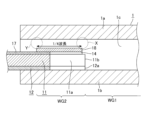
- the microstrip line-waveguide converter according to Embodiment 1 includes one end of a waveguide (hereinafter referred to as waveguide 1) and a converter formed at one end of a microstrip substrate. .
- the waveguide 1 has an upper wall 1a, a lower wall 1b, a right side wall 1c, and a left side wall 1d, and has a transducer forming area at one end.
- the waveguide 1 propagates electromagnetic waves, which are high-frequency signals converted by the microstrip line-waveguide converter, in an electromagnetic wave propagation region communicating from the transducer formation region.
- the waveguide 1 has a rectangular cross section, and the width of the right side wall 1c and the left side wall 1d is shorter than the width of the upper wall 1a and the lower wall 1b.
- the upper, lower, left, and right of the upper wall 1a, the lower wall 1b, the right side wall 1c, and the left side wall 1d are added for convenience of explanation, and the upper wall 1a and the lower wall 1b are a pair of side walls, and the right side wall 1c and the left side wall 1d. may be the upper wall and the lower wall.
- the width of the pair of side walls is narrower than the width of the upper wall and the lower wall.
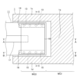
- the conversion section formed at one end of the microstrip substrate includes a dielectric 11, a first ground conductor 12, a plurality of right through conductors 13, a right ground conductor pad 14, a plurality of left through conductors 15, It includes a left ground conductor pad 16, a signal conductor 17, and a second ground conductor 18.
- the height of the conversion section is shorter than the distance from the inner surface of the lower wall 1b to the inner surface of the upper wall 1a in the waveguide 1.
- the dielectric 11 is a dielectric formed continuously with the dielectric of the microstrip substrate.
- the dielectric 11 is arranged at one end of the waveguide 1, that is, in the transducer formation region, and is fixed to the inner surface of the one end of the lower wall 1b of the waveguide 1 via the first ground conductor 12.
- the dielectric 11 has a cutout 11a that communicates with the waveguide 1 at one end thereof, and has a right side 11b and a left side 11c on each side of the cutout 11a.
- the cutout portion 11a penetrates from the front surface to the back surface of the dielectric 11, and the front surface, the back surface, and the end surface communicating with the waveguide 1 are exposed surfaces.
- the exposed surface on the back side of the notch portion 11a is covered by the lower wall 1b of the waveguide 1.
- the dielectric 11 is, for example, ceramic, which is commonly used in microstrip substrates.
- the first ground conductor 12 is formed on the back surface of the dielectric 11, and one end thereof is electrically and mechanically connected to the inner surface of one end of the lower wall 1b of the waveguide 1 by solder or the like.
- the first ground conductor 12 has a right ground conductor 12a formed on the back surface of the right side 11b of the dielectric 11, and a left ground conductor 12b formed on the back surface of the left side 11c of the dielectric 11.
- the first ground conductor 12 is waveguided parallel to the tube axis of the waveguide 1, specifically, so that the longitudinal direction of the right ground conductor 12a and the left side portion 11c is parallel to the tube axis of the waveguide 1. It is electrically and mechanically connected to the inner surface at one end of the lower wall 1b of the tube 1.
- the first ground conductor 12 is a conductive foil formed continuously with the ground conductor formed on the back surface of the dielectric of the microstrip substrate.
- the plurality of right through conductors 13 each penetrate the right side 11b of the dielectric 11 from the front surface to the back side, are arranged in parallel at equal intervals along the right side 11b, and have their lower ends connected to the right ground conductor of the first ground conductor 12. 12a.
- the plurality of right penetrating conductors 13 are arranged parallel to the tube axis of the waveguide 1 at equal intervals.
- the right ground conductor pad 14 is formed on the surface of the right side 11b of the dielectric 11, is electrically connected to the upper end of the plurality of right through conductors 13, and is connected to the first ground conductor 12 via the plurality of right through conductors 13. is electrically connected to the right ground conductor 12a.
- the longitudinal center axis of the right conductor pad 14 is parallel to the tube axis of the waveguide 1 .
- the electrical connection between the right ground conductor 12a and the right ground conductor pad 14 is preferably made by a plurality of right through conductors 13 arranged at equal intervals parallel to the tube axis of the waveguide 1;
- the right ground conductor 12a and the right ground conductor pad 14 may be electrically connected by the right through conductor 13.
- electrical connection between the right ground conductor 12a and the right ground conductor pad 14 is made by at least one right through conductor 13.
- the plurality of left through conductors 15 each penetrate the left side 11c of the dielectric 11 from the front surface to the back side, are arranged in parallel at equal intervals along the left side 11c, and have their lower ends connected to the left ground conductor 12b of the first ground conductor 12. electrically connected to.
- the plurality of left penetrating conductors 15 are arranged parallel to the tube axis of the waveguide 1 at equal intervals.
- the left ground conductor pad 16 is formed on the surface of the left side 11 c of the dielectric 11 , is electrically connected to the upper ends of the plurality of left through conductors 15 , and is connected to the first ground conductor 12 via the plurality of left through conductors 15 . is electrically connected to the left ground conductor 12b.
- the longitudinal central axis of the left conductor pad 16 is parallel to the tube axis of the waveguide 1 .
- the electrical connection between the left ground conductor 12b and the left ground conductor pad 16 is preferably made by a plurality of left through conductors 15 arranged at equal intervals parallel to the tube axis of the waveguide 1;
- the left ground conductor 12b and the left ground conductor pad 16 may be electrically connected by the left through conductor 15.
- the electrical connection between the left ground conductor 12b and the left ground conductor pad 16 is made by at least one left through conductor 15.
- the plurality of right through conductors 13 and the plurality of left through conductors 15 are formed, for example, in the same manner as a generally known method of forming vias (VIA) in a dielectric material constituting a substrate.
- the right ground conductor pad 14 and the left ground conductor pad 16 are formed, for example, in the same manner as a generally known method of forming a conductive foil on a dielectric material constituting a substrate.
- the signal conductor 17 is formed on the surface of the dielectric 11, and one end reaches a notch 11a formed in the dielectric 11.
- the signal conductor 17 is a line parallel to the tube axis of the waveguide 1.
- the signal conductor 17 is a conductive foil formed continuously with the signal conductor formed on the dielectric surface of the microstrip substrate.
- a signal conductor, a dielectric material, and a ground conductor constitute a microstrip line.
- the signal conductor 17, dielectric 11, and first ground conductor 12 constitute a microstrip line continuous from the microstrip line on the microstrip board.
- the second ground conductor 18 covers the exposed surface of the dielectric 11 on the front side of the notch 11a.
- the back surface of the right side is electrically and mechanically connected to the surface of the right ground conductor pad 14
- the back surface of the left side is electrically and mechanically connected to the surface of the left ground conductor pad 16.
- the back surface of the other end is electrically and mechanically connected to the surface of one end of the signal conductor 17.
- a gap exists between the surface of the second ground conductor 18 and the inner surface of the upper wall 1a of the waveguide 1.
- the length of the second ground conductor 18 in the tube axis direction of the waveguide 1 is 1/4 wavelength of the signal propagating through the waveguide 1 .
- the lower wall 1b, the second ground conductor 18, the right ground conductor 12a, the plurality of right through conductors 13, the right ground conductor pad 14, the left ground conductor 12b, the plurality of left through conductors 15, and the left ground conductor pad 16 constitutes a conversion waveguide WG2 in the conversion section.
- the conversion waveguide WG2 is a hollow waveguide surrounding the notch 11a, and has a relatively high impedance characteristic.
- the other end side of the waveguide 1 from the end face communicating with the waveguide 1 in the notch portion 11a constitutes a propagation waveguide WG1. It is necessary to impedance match the conversion waveguide WG2 and the propagation waveguide WG1, and since the conversion waveguide WG2 is a waveguide with relatively high impedance characteristics, the propagation waveguide WG1 It can also be made into a waveguide with relatively high impedance characteristics.
- Both the conversion waveguide WG2 and the propagation waveguide WG1 are waveguides with high impedance characteristics by making the minimum interval so that they do not electrically short-circuit (in other words, maintain an open state). Therefore, impedance matching between the propagation waveguide WG1 and the conversion waveguide WG2 becomes good.
- the distance from the inner surface of the lower wall 1b of the waveguide 1 to the inner surface of the upper wall 1a of the waveguide 1 can be made the same in the conversion waveguide WG2 and the propagation waveguide WG1, There is no need to make any special modifications to the waveguide 1. Note that the wavelength of the high frequency signal propagating through the conversion waveguide WG2 and the wavelength of the high frequency signal propagating through the propagation waveguide WG1 are the same.
- the conversion waveguide WG2 is electrically connected to the microstrip line on the microstrip board by having the other end of the second ground conductor 18 electrically connected to the signal conductor 17. .
- the length in the tube axis direction of the waveguide 1 in the second ground conductor 18 is 1/4 wavelength of the signal propagating through the waveguide 1, one end of the second ground conductor 18 and the waveguide
- the upper wall 1a of the waveguide 1 is electrically short-circuited to the signal propagating through the waveguide 1 (section X in FIGS. 2 and 3). That is, the conversion waveguide WG2 is electrically connected to the propagation waveguide WG1 at one end for a signal propagating through the waveguide 1.
- the conversion waveguide WG2 in the conversion section transmits the high frequency signal transmitted through the microstrip line in the microstrip board at the location where the signal conductor 17 and the second ground conductor 18 are electrically connected, that is, at the connection section.
- the waveguide 1 is converted into a high frequency signal that propagates, and the converted high frequency signal is propagated to the propagation waveguide WG1 in the waveguide 1. Note that since a gap exists between the other end of the second ground conductor 18 and the upper wall 1a of the waveguide 1, there is a gap between the other end of the second ground conductor 18 and the upper wall 1a of the waveguide 1.
- 1a is an electrically open state (section Y shown in FIGS. 2 and 3).
- One end of the dielectric constituting the microstrip substrate is used as a transducer forming region for forming a microstrip line-waveguide converter.
- the dielectric in the transducer forming region is the dielectric 11 in the microstrip line-waveguide converter.
- a notch 11a is formed in the dielectric 11.
- a first ground conductor 12 is formed on the back surface of the dielectric 11 at the same time as the ground conductor on the microstrip substrate.
- a plurality of right through conductors 13 and a plurality of left through conductors 15 are formed simultaneously with vias (VIAs) which are through conductors in the microstrip substrate.
- VIPs vias
- a right ground conductor pad 14, a left ground conductor pad 16, and a signal conductor 17 are arranged on the surface of a dielectric material constituting a microstrip board as wiring layers and microstrip lines for various high frequency circuits for signal processing and their peripheral circuits. Formed at the same time as the signal conductor constituting the
- the conductor 17 can be formed in the process of forming the microstrip substrate.
- the second ground conductor 18 is placed to cover the exposed surface of the front side of the notch 11a in the dielectric 11, so that the back surface of the right side is the surface of the right ground conductor pad 14, and the back surface of the left side is the left ground conductor.
- the front surface of the pad 16 and the back surface of the other end are electrically and mechanically connected to the surface of one end of the signal conductor 17.
- a microstrip line-waveguide converter can be formed at one end of the microstrip substrate, and the signal conductor 17 in the microstrip line-waveguide converter constitutes a microstrip line in the microstrip substrate. Formed continuously with the signal conductor.
- a microstrip line-waveguide converter formed at one end of the microstrip substrate is inserted into one end of the waveguide 1, and one end of the first ground conductor 12 is connected to the bottom wall 1b of the waveguide 1. Connect electrically and mechanically to the inner surface of one end using solder or the like. Thereby, the microstrip line-waveguide converter is attached to one end of the waveguide 1. Furthermore, a conversion waveguide WG2 which is a hollow waveguide surrounding the notch 11a is formed, and one end of the second ground conductor 18 is connected to the upper wall 1a of the waveguide 1 for signals propagating through the waveguide 1. There will be an electrical short circuit.
- the microstrip line-waveguide converter is connected to the waveguide 1 in a state in which a high frequency signal can be propagated.
- the microstrip line-waveguide converter and the waveguide 1 can be connected, and assembly is easy.
- the gap absorbs the combined dimensional error, for example ⁇ 50 ⁇ m, so the microstrip line-waveguide converter is When attached to the waveguide 1, no stress is applied to the second ground conductor 18 and the upper wall 1a of the waveguide 1.
- the microstrip line-waveguide converter, the microstrip substrate, and the waveguide 1 are not damaged. Furthermore, since the height of the waveguide 1 can be increased, the ratio of dimensional error to the height of the waveguide 1 is small, and the change in electrical characteristics as a microstrip line-waveguide converter is small.
- the high frequency signal transmitted through the microstrip line on the microstrip substrate is transmitted to the microstrip line including the signal conductor 17 in the microstrip line-waveguide converter.
- the high frequency signal transmitted to the microstrip line including the signal conductor 17 is converted to surround the notch 11a at the point where one end of the signal conductor 17 and the other end of the second ground conductor 18 are electrically connected.
- waveguide WG2. The converted high-frequency signal propagates through the conversion waveguide WG2.
- the high frequency signal (electromagnetic wave) propagated through the conversion waveguide WG2 is transmitted through the waveguide 1 from one end of the second ground conductor 18, which is electrically short-circuited to the signal propagated through the waveguide 1. It propagates to the waveguide WG1.
- a gap exists between the surface of the second ground conductor 18 and the inner surface of the upper wall 1a of the waveguide 1, and the second ground conductor Since the length of the waveguide 1 in the tube axis direction at 18 is 1/4 wavelength of the signal propagating through the waveguide 1, one end of the second ground conductor 18 is guided to the upper wall 1a of the waveguide 1.
- the current flowing through the second ground conductor 18 due to the high frequency signal transmitted to the microstrip line including the signal conductor 17 which is electrically short-circuited with respect to the signal propagating through the wave tube 1 is connected to one end of the second ground conductor 18.
- the high frequency signal flows from the waveguide 1 to the upper wall 1a of the waveguide 1, and is propagated to the propagation waveguide WG1 of the waveguide 1.
- the high frequency signal propagating through the conversion waveguide WG2 constituted by the second ground conductor 18 etc. is transmitted from the air gap between the surface of the second ground conductor 18 and the inner surface of the upper wall 1a of the waveguide 1. Will not leak.
- the high frequency signal propagating through the conversion waveguide WG2 is propagated with low loss and is propagated to the propagation waveguide WG1 of the waveguide 1.
- the advantages of providing the conversion waveguide WG2 surrounding the cutout portion 11a will be described below.
- the conversion waveguide WG2 in the first embodiment does not have the notch 11a, that is, the dielectric 11 remains.
- An example using a conversion waveguide WG3 which is a resin waveguide will be shown.
- the conversion waveguide WG3 includes a first ground conductor 12, a second ground conductor 18, a plurality of right through conductors 13, a right ground conductor pad 14, a plurality of left through conductors 15, and a left ground conductor pad 16. Ru.
- the conversion waveguide WG3 is a resin waveguide that surrounds the material of the dielectric 11, and has a relative dielectric constant larger than that of the hollow 1, and furthermore, since the thickness of the dielectric 11 is generally thin, the impedance is low. It becomes a waveguide with extremely low impedance characteristics.
- the distance H2 in the propagation waveguide WG1 is shorter than the thickness of the dielectric 11.
- the distance H2 in the propagation waveguide WG1 is very small, and the height of the waveguide 1 is also inevitably low.
- the microstrip line-waveguide converter according to Embodiment 1 from the inner surface of the waveguide 1 to the lower wall 1b of the waveguide 1 in the conversion waveguide WG2 to the inner surface of the upper wall 1a of the waveguide 1.
- the distance from the inner surface to the lower wall 1b of the waveguide 1 in the propagation waveguide WG1 to the inner surface of the upper wall 1a of the waveguide 1 can be made the same, and the dimensional error with respect to the height of the waveguide 1 can be made the same.
- the change in electrical characteristics of the microstrip line-waveguide converter due to dimensional errors is small.
- the microstrip line-waveguide converter according to the first embodiment can reduce changes in electrical characteristics due to dimensional errors in the height direction from the inner surface of the lower wall 1b of the waveguide 1.
- the microstrip line-waveguide converter has the notch 11a at one end of the dielectric 11, and the lower wall 1b of the waveguide 1 and the second A hollow conductor that surrounds the notch 11a is formed by the ground conductor 18, the right ground conductor 12a, the plural right through conductors 13, the right ground conductor pad 14, the left ground conductor 12b, the plural left through conductors 15, and the left ground conductor pad 16.
- One end of the first ground conductor 12 formed on the back surface of the dielectric 11 constitutes the conversion waveguide WG2, which is a wave tube, and electrically and mechanically connects to the inner surface of one end of the lower wall 1b of the waveguide.
- the microstrip line-waveguide converter is attached to the waveguide 1 by connecting the microstrip line to the waveguide 1, and the other end of the second ground conductor 18 is electrically connected to one end of the signal conductor 17.
- the microstrip line-waveguide converter and the microstrip line on the microstrip board are connected, and the length of the second ground conductor 18 in the tube axis direction of the waveguide 1 propagates through the waveguide 1. Since the microstrip line-waveguide converter and waveguide 1 are connected as a quarter wavelength of the signal, the microstrip line and waveguide 1 on the microstrip substrate of the microstrip line-waveguide converter are connected. Easy to assemble.
- the microstrip line-waveguide converter according to the first embodiment has a gap between the surface of the second ground conductor 18 and the inner surface of the upper wall 1a of the waveguide 1, the dielectric 11 Even if there is a thickness error in the second ground conductor 18, or an error in the distance from the lower wall 1b to the upper wall 1a of the waveguide 1, the air gap absorbs the combined dimensional error, so the micro When attaching the strip line-waveguide converter to the waveguide 1, no stress is applied to the second ground conductor 18 and the upper wall 1a of the waveguide 1, and the microstrip line-waveguide converter and The microstrip substrate and waveguide 1 will not be damaged.
- the microstrip line-waveguide converter according to the first embodiment configures the conversion waveguide WG2 which is a hollow waveguide
- the conversion waveguide WG2 is a high-impedance characteristic guide.
- the propagation waveguide WG1 in the waveguide 1 can be a waveguide with high impedance characteristics, and the height of the waveguide 1 can be increased, so the dimensional error in the height of the waveguide 1 can be reduced. Since the ratio of 1 to 1 is small, changes in the electrical characteristics of the microstrip line-to-waveguide converter due to dimensional errors in the height direction from the inner surface of the lower wall 1b of the waveguide 1 can be reduced.
- the current flowing through the second ground conductor 18 due to the high frequency signal transmitted to the microstrip line including the signal conductor 17 is The high-frequency signal flows from one end of the waveguide 18 to the upper wall 1a of the waveguide 1, and is propagated to the propagation waveguide WG1 of the waveguide 1. Even though a gap is provided between the wall 1a and the inner surface of the wall 1a, the high frequency signal propagating through the conversion waveguide WG2 does not leak from the gap, and the high frequency signal propagating through the conversion waveguide WG2 has a wide band. and propagates with low loss.
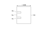
- the second ground conductor 18 in the microstrip line-waveguide converter according to the first embodiment is a second ground conductor 18 having slits 18b and 18c parallel to one end of the signal conductor 17, as shown in FIG. It is also possible to use the second ground conductor 18A.
- the second ground conductor 18A shown in FIG. It has slits 18b and 18c.
- the impedance matching from the microstrip line to the conversion waveguide WG2 on the microstrip board can be set better, and the impedance matching can be set better for broadband high-frequency signals. Reflective properties can be obtained.
- the number of slits 18b and 18c is not limited to two, and may be one or three or more. Considering the impedance matching between the microstrip line and the conversion waveguide WG2 on the microstrip board, the number of slits is Just choose the number, location, and dimensions appropriately.
- 1/4 wavelength includes not only 1/4 wavelength but also odd multiples of 1/4 wavelength.
- Embodiment 2 A microstrip line-waveguide converter according to Embodiment 2 will be explained using FIG. 10.
- the microstrip line-waveguide converter according to the second embodiment has a flat inner surface of the upper wall 1a of the waveguide 1 in the microstrip line-waveguide converter according to the first embodiment. The difference is that a step is provided, but the other points are the same. Note that in FIG. 10, the same reference numerals as those shown in FIGS. 1 to 4 indicate the same or corresponding parts.
- the upper wall 1a of the waveguide 1 which is different from the microstrip line-waveguide converter according to the first embodiment, will be mainly described below.
- the distance h2 from the surface of the signal conductor 17 at a position not connected to the second ground conductor 18 to the inner surface 1a2 of the upper wall 1a of the waveguide 1 is It is longer than the distance h1 from the surface of the ground conductor 18 to the inner surface 1a1 of the upper wall 1a of the waveguide 1.
- the entire upper wall 1a from a plane perpendicular to the tube axis of the waveguide 1 including the other end surface of the second ground conductor 18 to one end surface of the waveguide 1.
- the thickness of the upper wall 1a is reduced to provide a step on the upper wall 1a, and the distance h2 is made longer than the distance h1.
- the gap between the microstrip line including the signal conductor 17 and the top wall 1a of the waveguide 1 is longer than the gap between the conversion waveguide WG2 and the top wall 1a of the waveguide 1.
- the air gap between the microstrip line including the signal conductor 17 and the upper wall 1a of the waveguide 1 extends from the surface of the signal conductor 17 constituting the microstrip line to the conversion waveguide WG2, that is, the second It is longer than the distance to the horizontal plane extending from the inner surface 1a1 of the upper wall 1a of the waveguide 1 located on the ground conductor 18.
- connection portion and the upper wall 1a of the waveguide 1 can be opened more reliably with respect to the high-frequency signal propagated to the conversion waveguide WG2.
- one end of the second ground conductor 18 and the upper wall 1a of the waveguide 1 are more reliably electrically short-circuited with respect to the signal propagating in the waveguide 1, and the surface of the second ground conductor 18 is It is possible to further reduce the leakage of the high frequency signal propagated to the conversion waveguide WG2 from the gap between the inner surface of the upper wall 1a of the waveguide 1, and to obtain a microstrip line-waveguide converter with lower loss. .
- the microstrip line-waveguide converter according to the second embodiment has the same effects as the microstrip line-waveguide converter according to the first embodiment, and also has the same effect as the high-frequency wave propagating through the conversion waveguide WG2. Signals can be propagated with lower loss.
- Embodiment 3 A microstrip line-waveguide converter according to Embodiment 3 will be explained using FIGS. 11 to 14.
- the microstrip line-waveguide converter according to the third embodiment has a stub dielectric 19 on the surface of the second ground conductor 18, unlike the microstrip line-waveguide converter according to the first embodiment.
- the difference is that the stub through conductor 20 and the stub conductor 21 are arranged, and the other points are the same.
- FIGS. 11 to 14 the same reference numerals as those shown in FIGS. 1 to 4 indicate the same or corresponding parts.
- the microstrip line-waveguide converter according to the third embodiment like the microstrip line-waveguide converter according to the first embodiment, has a waveguide 1 formed at one end of the microstrip substrate. and a conversion unit.
- the waveguide 1 has an upper wall 1a, a lower wall 1b, a right side wall 1c, and a left side wall 1d, and transmits electromagnetic waves that are high frequency signals.
- the waveguide 1 has a rectangular cross section, and the width of the upper wall 1a and the lower wall 1b is longer than the width of the right side wall 1c and the left side wall 1d.
- the conversion section includes a dielectric 11, a first ground conductor 12, a plurality of right through conductors 13, a right ground conductor pad 14, a plurality of left through conductors 15, a left ground conductor pad 16, and a signal conductor. 17, a second ground conductor 18, a stub dielectric 19, a stub through conductor 20, and a stub conductor 21.
- the height of the conversion section is shorter than the distance from the inner surface of the lower wall 1b to the inner surface of the upper wall 1a in the waveguide 1.
- Reference numeral 18 indicates the dielectric 11, the first ground conductor 12, the plurality of right through conductors 13, the right ground conductor pad 14, and the plurality of left through conductors in the conversion part of the microstrip line-waveguide converter according to the first embodiment.
- the conductor 15, the left ground conductor pad 16, the signal conductor 17, and the second ground conductor 18 are the same or substantially the same.
- the dielectric 11 is a dielectric formed continuously with the dielectric of the microstrip substrate, and is disposed at the end of the waveguide 1, and has a notch 11a communicating with the waveguide 1 at one end.
- the cutout portion 11a has a right side portion 11b and a left side portion 11c on each side of the cutout portion 11a.
- the first ground conductor 12 is formed on the back surface of the dielectric 11, and one end thereof is electrically and mechanically connected to the inner surface of one end of the lower wall 1b of the waveguide 1.
- the first ground conductor 12 has a right ground conductor 12a formed on the back surface of the right side 11b of the dielectric 11, and a left ground conductor 12b formed on the back surface of the left side 11c of the dielectric 11.
- the first ground conductor 12 is a conductive foil formed continuously with the ground conductor formed on the back surface of the dielectric of the microstrip substrate.
- the plurality of right through conductors 13 each penetrate the right side 11b of the dielectric 11 from the front surface to the back side, are arranged in parallel at equal intervals along the right side 11b, and have their lower ends connected to the right ground conductor of the first ground conductor 12. 12a.
- the right ground conductor pad 14 is formed on the surface of the right side 11b of the dielectric 11, is electrically connected to the upper end of the plurality of right through conductors 13, and is connected to the first ground conductor 12 via the plurality of right through conductors 13. is electrically connected to the right ground conductor 12a.
- the plurality of left through conductors 15 each penetrate the left side 11c of the dielectric 11 from the front surface to the back side, are arranged in parallel at equal intervals along the left side 11c, and have their lower ends connected to the left ground conductor 12b of the first ground conductor 12. electrically connected to.
- the left ground conductor pad 16 is formed on the surface of the left side 11 c of the dielectric 11 , is electrically connected to the upper ends of the plurality of left through conductors 15 , and is connected to the first ground conductor 12 via the plurality of left through conductors 15 . is electrically connected to the left ground conductor 12b.
- the signal conductor 17 is formed on the surface of the dielectric 11, and one end reaches a notch 11a formed in the dielectric 11.
- the signal conductor 17 is a line parallel to the tube axis of the waveguide 1.
- the signal conductor 17 is a conductive foil formed continuously with the signal conductor formed on the dielectric surface of the microstrip substrate.
- the signal conductor 17, the dielectric 11, and the first ground conductor 12 constitute a microstrip line continuous from the microstrip line on the microstrip board.
- the second ground conductor 18 covers the exposed surface of the dielectric 11 on the front side of the notch 11a.
- the back surface of the right side is electrically and mechanically connected to the surface of the right ground conductor pad 14
- the back surface of the left side is electrically and mechanically connected to the surface of the left ground conductor pad 16.
- the back surface of the other end is electrically and mechanically connected to the surface of one end of the signal conductor 17.
- the lower wall 1b, the second ground conductor 18, the right ground conductor 12a, the plurality of right through conductors 13, the right ground conductor pad 14, the left ground conductor 12b, the plurality of left through conductors 15, and the left ground conductor pad 16 constitutes a conversion waveguide WG2 in the conversion section.
- the conversion waveguide WG2 is a hollow waveguide surrounding the notch 11a, and has a relatively high impedance characteristic. Since the conversion waveguide WG2 has a relatively high impedance characteristic, the propagation waveguide WG1 in the waveguide 1 can also easily obtain a relatively high high impedance characteristic, and the propagation waveguide WG1 and the conversion waveguide It is easy to match the impedance of tube WG2.
- the back surface of the stub dielectric 19 is joined to the surface of the second ground conductor 18 .
- the stub dielectric 19 is, for example, ceramic like the dielectric 11.
- the length of the waveguide 1 in the tube axis direction and the width perpendicular to the tube axis direction in the stub dielectric 19 are the same as the length in the tube axis direction of the waveguide 1 in the second ground conductor 18 and the width in the tube axis direction of the waveguide 1 in the second ground conductor 18. It is the same as the length of the width perpendicular to the axial direction.
- the size of the stub dielectric 19 does not necessarily have to be the same as the size of the second ground conductor 18, and may be slightly smaller.
- the stub through conductor 20 is located at the center in the width direction of one end of the stub dielectric 19, penetrates from the front surface to the back surface of the stub dielectric 19, and has a lower end electrically connected to the second ground conductor 18. Ru.
- the stub through conductor 20 is formed, for example, in the same manner as a generally known method of forming vias (VIA) in a dielectric material constituting a multilayer wiring board.
- the back surface of the stub conductor 21 is joined to the surface of the stub dielectric 19.
- the stub conductor 21 is electrically connected to the second ground conductor 18 on the back surface of one end by the stub penetrating conductor 20 .
- a gap exists between the surface of the stub conductor 21 and the inner surface of the upper wall 1a of the waveguide 1.
- the length in the tube axis direction of the waveguide 1 in the stub conductor 21 is the length from the connection part 20a between the lower end of the stub penetrating conductor 20 and the surface of the second ground conductor 18 to the other end of the stub conductor 21.
- the wavelength is determined to be 1/4 wavelength of the signal propagating through the waveguide 1.
- connection part 20a between the lower end of the stub through conductor 20 and the surface of the second ground conductor 18, the stub through conductor 20, and the upper end of the stub through conductor 20 and one end of the back surface of the stub conductor 21.
- the length from the connecting portion 20b to the other end of the stub conductor 21 is 1/4 wavelength of the signal propagating through the waveguide 1. Therefore, the stub dielectric 19, the stub through conductor 20, the stub conductor 21, and the second ground conductor 18 operate as a 1/4 wavelength stub with an open end in the conversion section.
- the other end of the stub conductor 21 and the upper wall 1a of the waveguide 1 are electrically It is in an open state (section Y shown in FIG. 13).
- the length from the connection part 20a between the lower end of the stub through conductor 20 and the surface of the second ground conductor 18 to the other end of the stub conductor 21 is 1/4 wavelength of the signal propagating through the waveguide 1. Therefore, the stub conductor 21 and the second ground conductor 18 operate as a 1/4 wavelength stub with an open end.
- the second ground conductor 18 and the stub conductor 21 operate as a 1/4 wavelength stub, one end of the second ground conductor 18 is connected to the upper wall 1a of the waveguide 1. This results in an electrical short circuit (section X in FIG. 13) for the signal propagating through.
- the conversion waveguide WG2 is electrically connected to the microstrip line on the microstrip substrate by electrically connecting the second ground conductor 18 to the signal conductor 17 at the other end.
- the conversion waveguide WG2 at one end of the conversion waveguide WG2, one end of the second ground conductor 18 and the upper wall 1a of the waveguide 1 are electrically short-circuited with respect to the signal propagating through the waveguide 1.
- it is electrically connected to the propagation waveguide WG1.
- the stub dielectric 19 is arranged in alignment with the second ground conductor 18 such that the back surface of the stub dielectric 19 is joined to the front surface of the second ground conductor 18 .
- a through conductor 20 for stub is formed.
- the stub dielectric 19 and the stub through conductor 20 are formed by a generally known method for forming a dielectric and a via (VIA) in a multilayer wiring board.
- the stub conductor 21 is formed on the surface of the stub dielectric 19 so as to be electrically connected to the upper end of the stub through conductor 20 .
- the stub conductor 21 is formed on the surface of the stub dielectric 19, for example, in the same manner as the generally known method of forming a conductor foil on a dielectric that constitutes a substrate.
- a microstrip line-to-waveguide converter having an open-ended 1/4 wavelength stub can be formed at one end of the microstrip substrate, and the signal conductor 17 in the microstrip line-to-waveguide converter can be formed at one end of the microstrip substrate. It is formed continuously with the signal conductor constituting the microstrip line on the microstrip board.
- a microstrip line-waveguide converter formed at one end of the microstrip substrate is inserted into one end of the waveguide 1, and one end of the first ground conductor 12 is connected to the bottom wall 1b of the waveguide 1. Connect electrically and mechanically to the inner surface of one end using solder or the like. Thereby, the microstrip line-waveguide converter is attached to one end of the waveguide 1. Furthermore, a conversion waveguide WG2, which is a hollow waveguide surrounding the notch 11a, is formed, and the stub conductor 21 and the second ground conductor 18 operate as a 1/4 wavelength stub with an open end. One end of the second ground conductor 18 and the upper wall 1a of the waveguide 1 are electrically short-circuited with respect to a signal propagating through the waveguide 1.
- the microstrip line-waveguide converter is connected to the waveguide 1 in a state in which a high frequency signal can be propagated.
- the microstrip line-waveguide converter is connected.
- the waveguide 1 can be connected and assembly is easy.
- the air gap absorbs the combined dimensional error, making it easy to guide the microstrip line-waveguide converter.
- the microstrip line-waveguide converter, the microstrip substrate, and the waveguide 1 are not damaged.
- the high frequency signal transmitted through the microstrip line on the microstrip substrate is transmitted to the microstrip line including the signal conductor 17 in the microstrip line-waveguide converter.
- the high frequency signal transmitted to the microstrip line including the signal conductor 17 is converted to surround the notch 11a at the point where one end of the signal conductor 17 and the other end of the second ground conductor 18 are electrically connected.
- waveguide WG2. The converted high-frequency signal propagates through the conversion waveguide WG2.
- the high frequency signal (electromagnetic wave) propagated through the conversion waveguide WG2 is guided from one end of the second ground conductor 18 which is electrically short-circuited to the signal propagated through the waveguide 1 by the stub conductor 21. It propagates to the propagation waveguide WG1 of the tube 1.
- a gap exists between the surface of the stub conductor 21 and the inner surface of the upper wall 1a of the waveguide 1, and the stub conductor 21 and the second Since the ground conductor 18 operates as a 1/4 wavelength stub with an open end, one end of the second ground conductor 18 is electrically connected to the upper wall 1a of the waveguide 1 for signals propagating through the waveguide 1.
- the current flowing through the second ground conductor 18 due to the short-circuited high-frequency signal transmitted to the microstrip line including the signal conductor 17 flows from one end of the second ground conductor 18 to the upper wall 1a of the waveguide 1, and the high-frequency The signal is propagated to the propagation waveguide WG1 of the waveguide 1.
- the high frequency signal propagating through the conversion waveguide WG2 constituted by the second ground conductor 18 etc. will not leak from the gap between the surface of the stub conductor 21 and the inner surface of the upper wall 1a of the waveguide 1. There is no.
- the high frequency signal propagating through the conversion waveguide WG2 is propagated with low loss and is propagated to the propagation waveguide WG1 of the waveguide 1.
- the microstrip line-waveguide converter according to the third embodiment is similar to the microstrip line-waveguide converter according to the first embodiment.
- the conversion waveguide WG2 which is a wave tube, is configured such that one end of the first ground conductor 12 formed on the back surface of the dielectric 11 is electrically and mechanically connected to the inner surface at one end of the lower wall 1b of the waveguide.
- the microstrip line-waveguide converter is attached to the waveguide 1 by connecting the microstrip line to the waveguide 1, and the other end of the second ground conductor 18 is electrically connected to one end of the signal conductor 17.
- the microstrip line-waveguide converter and the microstrip line on the microstrip board are connected, and the stub conductor 21, which operates as an open-ended 1/4 wavelength stub, and the second ground conductor 18 are connected to the second ground conductor 18. Since it is arranged on the surface of the ground conductor 18, it is easy to assemble the microstrip line-waveguide converter to the microstrip line and waveguide 1 on the microstrip substrate.
- the microstrip line-waveguide converter according to the third embodiment has a gap between the surface of the stub conductor 21 and the inner surface of the upper wall 1a of the waveguide 1, the thickness of the dielectric 11 can be reduced. Even if there is an error, a thickness error of the second ground conductor 18, an error in the distance from the lower wall 1b to the upper wall 1a of the waveguide 1, or a thickness error in the stub dielectric 19, the combined dimensional error When the microstrip line-waveguide converter is attached to the waveguide 1, the air gap absorbs the No stress is applied and the microstrip line-waveguide converter, microstrip substrate, and waveguide 1 are not damaged.
- the microstrip line-waveguide converter according to the third embodiment configures the conversion waveguide WG2 which is a hollow waveguide
- the conversion waveguide WG2 is a guide with high impedance characteristics.
- the propagation waveguide WG1 in the waveguide 1 can be a waveguide with high impedance characteristics, and the height of the waveguide 1 can be increased, so the dimensional error in the height of the waveguide 1 can be reduced. Since the ratio of 1 to 1 is small, changes in the electrical characteristics of the microstrip line-to-waveguide converter due to dimensional errors in the height direction from the inner surface of the lower wall 1b of the waveguide 1 can be reduced.
- the current flowing through the second ground conductor 18 due to the high frequency signal transmitted to the microstrip line including the signal conductor 17 is Since the conductor 18 and the stub conductor 21 operate as a 1/4 wavelength stub with an open end, a high-frequency signal flows from one end of the second ground conductor 18 to the upper wall 1a of the waveguide 1, and the high-frequency signal propagates through the waveguide 1. Even though a gap is provided between the surface of the stub conductor 21 and the inner surface of the upper wall 1a of the waveguide 1, the signal propagates through the conversion waveguide WG2. The high frequency signal does not leak from the gap, and the high frequency signal propagating through the conversion waveguide WG2 propagates in a wide band and with low loss.
- the second ground conductor 18 in the microstrip line-waveguide converter according to the third embodiment is a second ground conductor 18 having slits 18b and 18c parallel to one end of the signal conductor 17, as shown in FIG. It is also possible to use the second ground conductor 18A.
- a second ground conductor 18A shown in FIG. 15 is provided on each side of the signal conductor connecting portion 18a that is electrically and mechanically connected to the surface of one end of the signal conductor 17 in parallel with the signal conductor connecting portion 18a. It has slits 18b and 18c.
- the impedance matching from the microstrip line to the conversion waveguide WG2 on the microstrip board can be set better, and the impedance matching can be set better for broadband high-frequency signals. Reflective properties can be obtained.
- the number of slits 18b and 18c is not limited to two, and may be one or three or more. Considering the impedance matching between the microstrip line and the conversion waveguide WG2 on the microstrip board, the number of slits 18b and 18c is not limited to two. Just choose the number, location, and dimensions appropriately.
- Embodiment 4 A microstrip line-waveguide converter according to Embodiment 4 will be explained using FIG. 16.
- the microstrip line-waveguide converter according to the fourth embodiment has a flat inner surface of the upper wall 1a of the waveguide 1 in the microstrip line-waveguide converter according to the third embodiment. The difference is that a step is provided, but the other points are the same.
- FIG. 16 the same reference numerals as those shown in FIGS. 11 to 14 indicate the same or equivalent parts.
- the upper wall 1a of the waveguide 1 which is different from the microstrip line-waveguide converter according to the third embodiment, will be mainly explained below.
- the distance h4 from the surface of the signal conductor 17 at a position not connected to the second ground conductor 18 to the inner surface 1a2 of the upper wall 1a of the waveguide 1 is equal to It is longer than the distance h3 from the surface of 21 to the inner surface 1a1 of the upper wall 1a of the waveguide 1.
- the upper wall 1a is made thinner, a step is provided on the upper wall 1a, and the distance h4 is made longer than the distance h3.
- the gap between the microstrip line including the signal conductor 17 and the top wall 1a of the waveguide 1 is longer than the gap between the conversion waveguide WG2 and the top wall 1a of the waveguide 1.
- the air gap between the microstrip line including the signal conductor 17 and the upper wall 1a of the waveguide 1 extends from the surface of the signal conductor 17 constituting the microstrip line to the conversion waveguide WG2, that is, the stub conductor. It is longer than the distance to the horizontal plane extending from the inner surface 1a1 of the upper wall 1a of the waveguide 1 located on the waveguide 21.
- the distance from the surface of the signal conductor 17 at a position not connected to the second ground conductor 18 to the inner surface of the upper wall 1a of the waveguide 1 is equal to the distance from the surface of the signal conductor 17 to the stub conductor 21.
- an open-ended 1/4 wavelength stub is formed by the stub conductor 21 and the second ground conductor 18. , the open end becomes more open, and one end of the second ground conductor 18, that is, the waveguide side, is more short-circuited to the upper wall 1a of the waveguide 1 with respect to the signal propagating in the waveguide 1. (short circuit), the leakage of high-frequency signals from the gap between the conversion waveguide WG2 and the upper wall 1a of the waveguide 1 can be further reduced, and a microstrip line-waveguide converter with lower loss can be achieved. can get.
- the microstrip line-waveguide converter according to the fourth embodiment has the same effect as the microstrip line-waveguide converter according to the third embodiment, and also has the same effect as the microstrip line-waveguide converter according to the third embodiment. Signals can be propagated with lower loss.
- the second ground conductor 18 is As shown in FIG. 15, the second ground conductor 18A may have slits 18b and 18c parallel to one end of the signal conductor 17.
- Embodiment 5 A microstrip line-waveguide converter according to Embodiment 5 will be explained using FIG. 17.
- the microstrip line-waveguide converter according to the fifth embodiment has a flat inner surface of the upper wall 1a of the waveguide 1 in the microstrip line-waveguide converter according to the third embodiment. The difference is that a step is provided, but the other points are the same. Note that in FIG. 17, the same reference numerals as those shown in FIGS. 11 to 14 indicate the same or equivalent parts.
- the inner surface 1a3 of the upper wall 1a of the waveguide 1 constituting the propagation waveguide WG1 is similar to the inner surface 1a3 of the upper wall 1a of the waveguide 1 where the conversion waveguide WG2 is located.
- the distance h5 from the inner surface of the lower wall 1b of the waveguide 1 constituting the propagation waveguide WG1 to the inner surface 1a3 of the upper wall 1a is below the waveguide 1 where the conversion waveguide WG2 is located. It is shorter than the distance h6 from the inner surface of the wall 1b to the inner surface 1a4 of the upper wall 1a.
- the dielectric 11 is arranged from a plane perpendicular to the tube axis of the waveguide 1 including one end surface of the dielectric 1 to one end surface of the waveguide 1.
- the entire thickness of the upper wall 1a is reduced at the position where the upper wall 1a is located, a step is provided on the upper wall 1a, and the distance h5 is made shorter than the distance h6.
- from the inner surface of the lower wall 1b of the waveguide 1 constituting the propagation waveguide WG1, that is, the lower wall 1b to which the first ground conductor 12 is not connected to the inner surface 1a3 of the upper wall 1a of the waveguide 1.
- the distance from the inner surface of the lower wall 1b of the waveguide 1 where the conversion waveguide WG2 is located to the surface of the second ground conductor 18 is made approximately the same.
- the gap between the surface of the stub conductor 21 and the inner surface 1a4 of the upper wall 1a of the waveguide 1 is narrowed, and the open end formed by the stub conductor 21 and the second ground conductor 18 is By shortening the distance between the 1/4 wavelength stub and the inner surface 1a3 of the upper wall 1a of the waveguide 1, one end of the second ground conductor 18 and the top of the waveguide 1 are connected to the signal propagating in the waveguide 1.
- a microstrip line-waveguide converter can be obtained.
- the second ground conductor 18 is As shown in FIG. 15, the second ground conductor 18A may have slits 18b and 18c parallel to one end of the signal conductor 17.
- the microstrip line-waveguide converter according to the fourth embodiment is not connected to the second ground conductor 18.
- the distance from the surface of the signal conductor 17 at the position to the inner surface of the upper wall 1a of the waveguide 1 extends from the surface of the signal conductor 17 to the inner surface of the upper wall of the waveguide located on the stub conductor 21. It may be longer than the distance to the horizontal plane.
- Embodiment 6 A microstrip line-waveguide converter according to Embodiment 6 will be explained using FIG. 18.
- the microstrip line-waveguide converter according to the sixth embodiment is different from the microstrip line-waveguide converter according to the third embodiment in that the stub conductor 21 and the second ground conductor 18 have an open end. Although a four-wavelength stub is configured, the stub conductor 21 and the second ground conductor 18 are configured to resonate within the stub dielectric 19 with respect to the frequency of the signal propagating through the waveguide 1. They are different and are otherwise the same. Note that in FIG. 18, the same reference numerals as those shown in FIGS. 11 to 14 indicate the same or equivalent parts.
- the dielectric for the stub will be explained with respect to the frequency of the signal propagating in the waveguide 1 using the stub conductor 21 and the second ground conductor 18, which are different from the microstrip line-waveguide converter according to the third embodiment.
- the configuration that causes resonance within 19 will be mainly explained.
- the back surface of the stub dielectric 19 is joined to the surface of the second ground conductor 18 .
- the stub dielectric 19 is, for example, ceramic like the dielectric 11.
- the length of the waveguide 1 in the tube axis direction and the width perpendicular to the tube axis direction in the stub dielectric 19 are the same as the length in the tube axis direction of the waveguide 1 in the second ground conductor 18 and the width in the tube axis direction of the waveguide 1 in the second ground conductor 18.
- the length of the width perpendicular to the axial direction is the same.
- the size of the stub dielectric 19 does not necessarily have to be the same as the size of the second ground conductor 18, and may be slightly smaller.
- the stub through conductor 20 is located at the center in the width direction of one end of the stub dielectric 19, penetrates from the front surface to the back surface of the stub dielectric 19, and has a lower end electrically connected to the second ground conductor 18. Ru.
- the stub through conductor 20 is formed, for example, in the same manner as a generally known method of forming a via (VIA) in a dielectric material constituting a multilayer wiring board.
- the back surface of the stub conductor 21 is joined to the surface of the stub dielectric 19.
- the stub conductor 21 is electrically connected to the second ground conductor 18 on the back surface of one end by the stub penetrating conductor 20 .
- a gap exists between the surface of the stub conductor 21 and the inner surface of the upper wall 1a of the waveguide 1.
- the stub conductor 21 cooperates with the second ground conductor 18 to cause resonance within the stub dielectric 19 with respect to the frequency of the signal propagating through the waveguide 1 . That is, the frequency of the signal propagating through the waveguide 1 resonates within the stub dielectric 19 surrounded by the stub conductor 21, the stub penetrating conductor 20, and the second ground conductor 18.
- the length of the stub conductor 21 in the tube axis direction of the waveguide 1 is determined to be a length at which the frequency of the signal propagating through the waveguide 1 resonates.
- the other end of the stub conductor 21 and the upper wall 1a of the waveguide 1 are electrically It is in an open state (section Y shown in FIG. 18).
- the frequency of the signal propagating through the waveguide 1 resonates within the stub dielectric 19 surrounded by the stub conductor 21, the stub through conductor 20, and the second ground conductor 18, so that as a result, the frequency of the signal propagating through the waveguide 1 resonates.
- One end of the second ground conductor 18 and the upper wall 1a of the waveguide 1 become electrically short-circuited (X section in FIG. 18) with respect to the signal propagating in the waveguide 1.
- the conversion waveguide WG2 is electrically connected to the microstrip line on the microstrip substrate by electrically connecting the second ground conductor 18 to the signal conductor 17 at the other end.
- the conversion waveguide WG2 at one end of the conversion waveguide WG2, one end of the second ground conductor 18 and the upper wall 1a of the waveguide 1 are electrically short-circuited with respect to the signal propagating through the waveguide 1.
- the signal propagating through the waveguide 1 is electrically connected to the propagation waveguide WG1.
- the microstrip line-waveguide converter according to the sixth embodiment is also easily assembled and operates similarly to the microstrip line-waveguide converter according to the third embodiment. and has a similar effect.
- the second ground conductor 18 is As shown in FIG. 15, the second ground conductor 18A may have slits 18b and 18c parallel to one end of the signal conductor 17.
- the microstrip line-waveguide converter is not connected to the second ground conductor 18.
- the distance from the surface of the signal conductor 17 at the position to the inner surface of the upper wall 1a of the waveguide 1 extends from the surface of the signal conductor 17 to the inner surface of the upper wall of the waveguide located on the stub conductor 21. It may be longer than the distance to the horizontal plane.
- the propagation waveguide in the waveguide 1 is The distance from the inner surface of the lower wall 1b of the waveguide 1 constituting WG1 to the inner surface 1a3 of the upper wall 1a is the distance from the inner surface of the lower wall 1b of the waveguide 1 where the conversion waveguide WG2 is located to the upper wall. It may be shorter than the distance to the inner surface 1a4 of 1a.
- Embodiment 7 A microstrip line-waveguide converter according to Embodiment 7 will be explained using FIGS. 19 to 22.
- the microstrip line-waveguide converter according to the seventh embodiment has a stub dielectric 19, a stub through conductor 20, and a stub conductor 21.
- the stub conductor 21 is disposed on the surface of the second ground conductor 18 with a gap between the surface of the stub conductor 21 and the inner surface of the upper wall 1a of the waveguide 1.
- the through conductor 20, the stub conductor 21, and the third ground conductor 22 are attached to the inner surface of the upper wall 1a of the waveguide 1 with a gap between the surface of the stub conductor 21 and the surface of the second ground conductor 18.
- the arrangement is different, and the other points are the same. Note that in FIGS. 19 to 22, the same reference numerals as those used in FIGS. 1 to 4 and FIGS. 11 to 14 indicate the same or equivalent parts.
- reference numeral 16 constitutes a conversion waveguide WG2 in the conversion section, which is a hollow waveguide surrounding the notch 11a.
- the conversion waveguide WG2 is electrically connected to the microstrip line on the microstrip board by electrically connecting the second ground conductor 18 to the signal conductor 17 at the other end.
- the stub dielectric 19, the stub through conductor 20, the stub conductor 21, and the third ground conductor 22 constitute a stub substrate that operates as a quarter-wavelength stub with an open end in the conversion section.
- the stub dielectric 19 is arranged so that its surface faces the surface of the second ground conductor 18 .
- the stub dielectric 19 is, for example, ceramic like the dielectric 11.
- the length of the waveguide 1 in the tube axis direction and the width perpendicular to the tube axis direction in the stub dielectric 19 are the same as the length in the tube axis direction of the waveguide 1 in the second ground conductor 18 and the width in the tube axis direction of the waveguide 1 in the second ground conductor 18. It is the same as the length of the width perpendicular to the axial direction.
- the size of the stub dielectric 19 does not necessarily have to be the same as the size of the second ground conductor 18, and may be slightly smaller.
- the stub dielectric 19 is fixed to the inner surface of one end of the upper wall 1 a of the waveguide 1 via the third ground conductor 22 . That is, the third ground conductor 22 is formed on the back surface of the stub dielectric, and the back surface is electrically and mechanically connected to the inner surface at one end of the upper wall 1a of the waveguide 1 by soldering or the like.
- the stub through conductor 20 is located at the center in the width direction of one end of the stub dielectric 19, penetrates from the front surface to the back surface of the stub dielectric 19, and has a lower end electrically connected to the third ground conductor 22. Ru.
- the stub through conductor 20 is formed, for example, in the same manner as a generally known method of forming a via (VIA) in a dielectric material.
- the stub conductor 21 has its front surface facing the surface of the second ground conductor 18 with a gap in between, and its back surface joined to the surface of the stub dielectric 19 .
- the stub conductor 21 is electrically connected to the third ground conductor 22 on the back surface of one end by the stub penetrating conductor 20 .
- the stub conductor 21 and the third ground conductor 22 are electrically connected by a stub through conductor 20 at the widthwise center of one end of the stub dielectric 19, and
- the length in the axial direction from the connection part 20a between the lower end of the through conductor 20 for stub and the surface of the third ground conductor 22 to the other end of the conductor 21 for stub is the length of the signal propagating through the waveguide 1.
- the wavelength is determined to be 1/4 wavelength.
- connection part 20a between the lower end of the through conductor 20 for stub and the surface of the third ground conductor 22 the through conductor 20 for stub, and the upper end of the through conductor 20 for stub and one end of the back surface of the conductor 21 for stub.
- the length from the connecting portion 20b to the other end of the stub conductor 21 is 1/4 wavelength of the signal propagating through the waveguide 1.
- the other end of the stub conductor 21 and the surface of the second ground conductor 18 are electrically open. state (section Y shown in FIG. 20).
- the length from the connection part 20a between the lower end of the through conductor 20 for stub and the surface of the third ground conductor 22 to the other end of the conductor 21 for stub is 1/4 wavelength of the signal propagating in the waveguide 1. Therefore, the stub conductor 21 and the third ground conductor 22 operate as a 1/4 wavelength stub with an open end. Therefore, one end of the second ground conductor 18 is electrically shorted (Fig. 20 (X section shown).
- one end of the second ground conductor 18 and the upper wall 1a of the waveguide 1 are electrically connected to the signal propagating in the waveguide 1 via the stub substrate. This causes a short circuit and the signal propagating through the waveguide 1 is electrically connected to the propagation waveguide WG1.
- a stub conductor 20 is formed to pass through the stub, and a stub conductor 21, which is a conductor foil, is formed on the surface of the stub dielectric 19 to produce a stub substrate that operates as a 1/4 wavelength stub with an open end.
- the third ground conductor 22, the stub through conductor 20, and the stub conductor 21 are formed on the stub dielectric 19 by a forming method generally known in this field.
- the third ground conductor 22 is electrically and mechanically connected to the set inner surface of the upper wall 1a of the waveguide 1 by soldering or the like, and the stub substrate is connected to the set inner surface of the upper wall 1a of the waveguide 1. It is fixed to one end of the upper wall 1a.
- a microstrip line-waveguide converter formed at one end of the microstrip substrate is inserted into one end of the waveguide 1, and the surface of the second ground conductor 18 is aligned with the third ground conductor 22 on the stub substrate.
- one end of the first ground conductor 12 is electrically and mechanically connected to the inner surface of one end of the lower wall 1b of the waveguide 1 by solder or the like.
- a conversion waveguide WG2 that is a hollow waveguide surrounding the notch 11a is formed, and a microstrip line-waveguide conversion in which a stub substrate is provided for the second ground conductor 18 is formed.
- the device is attached to one end of the waveguide 1.
- the stub substrate which operates as a 1/4 wavelength stub with an open end, allows one end of the second ground conductor 18 and the upper wall 1a of the waveguide 1 to be electrically connected to the signal propagating through the waveguide 1.
- a short circuit occurs, and the microstrip line-waveguide converter is connected to the waveguide 1 in a state where a high frequency signal can be propagated.
- the third ground conductor 22 on the stub board is electrically and mechanically connected to the inner surface of one end of the upper wall 1a of the waveguide 1 by solder or the like, and the first ground conductor 12
- the microstrip line-waveguide converter and the waveguide 1 can be connected by electrically and mechanically connecting one end to the inner surface of the lower wall 1b of the waveguide 1 using solder or the like. , easy to assemble.
- the high frequency signal transmitted through the microstrip line on the microstrip substrate is transmitted to the microstrip line including the signal conductor 17 in the microstrip line-waveguide converter.
- the high frequency signal transmitted to the microstrip line including the signal conductor 17 is converted to surround the notch 11a at the point where one end of the signal conductor 17 and the other end of the second ground conductor 18 are electrically connected.
- waveguide WG2. The converted high-frequency signal propagates through the conversion waveguide WG2.
- the high frequency signal (electromagnetic wave) propagated through the conversion waveguide WG2 is guided through the stub substrate from one end of the second ground conductor 18, which is electrically short-circuited to the signal propagated through the waveguide 1. It propagates to the propagation waveguide WG1 of the tube 1.
- a gap exists between the surface of the stub conductor 21 and the surface of the second ground conductor 18, and the gap exists between the stub conductor 21 and the third ground conductor 18. Since the conductor 22 operates as a 1/4 wavelength stub with an open end, one end of the second ground conductor 18 is electrically shorted to the upper wall 1a of the waveguide 1 with respect to the signal propagating in the waveguide 1. The current flowing through the second ground conductor 18 due to the high frequency signal transmitted to the microstrip line including the signal conductor 17 flows from one end of the second ground conductor 18 to the upper wall 1a of the waveguide 1 via the stub substrate. The high frequency signal is propagated to the propagation waveguide WG1 of the waveguide 1.
- the high frequency signal propagating through the conversion waveguide WG2 constituted by the second ground conductor 18 etc. does not leak from the gap between the surface of the stub conductor 21 and the surface of the second ground conductor 18. .
- the high frequency signal propagating through the conversion waveguide WG2 is propagated with low loss and is propagated to the propagation waveguide WG1 of the waveguide 1.
- the microstrip line-waveguide converter according to the seventh embodiment is similar to the microstrip line-waveguide converter according to the third embodiment.
- the conversion waveguide WG2 which is a wave tube, is configured such that one end of the first ground conductor 12 formed on the back surface of the dielectric 11 is electrically and mechanically connected to the inner surface at one end of the lower wall 1b of the waveguide.
- the microstrip line-waveguide converter is attached to the waveguide 1 by the electrical connection, and the other end of the second ground conductor 18 is electrically connected to one end of the signal conductor 17.
- the microstrip line-waveguide converter and the microstrip line on the microstrip board are connected, and the stub conductor 21, which operates as a 1/4 wavelength stub with an open end, and the third ground conductor 22 are connected to the waveguide. 1, it is easy to assemble the microstrip line-waveguide converter to the microstrip line and waveguide 1 on the microstrip substrate.
- the microstrip line-waveguide converter according to the seventh embodiment has a gap between the surface of the stub conductor 21 and the surface of the second ground conductor 18, the thickness error of the dielectric 11, Even if there is an error in the thickness of the second ground conductor 18, an error in the distance from the lower wall 1b to the upper wall 1a of the waveguide 1, or an error in the thickness of the stub dielectric 19, the combined dimensional error is
- the microstrip line-waveguide converter is attached to the waveguide 1, stress is applied to the stub dielectric 19, the second ground conductor 18, and the upper wall 1a of the waveguide 1. Therefore, the microstrip line-waveguide converter, the microstrip substrate, and the waveguide 1 will not be damaged.
- the conversion waveguide WG2 is a hollow waveguide
- the conversion waveguide WG2 is a guide with high impedance characteristics.
- the propagation waveguide WG1 in the waveguide 1 can be a waveguide with high impedance characteristics, and the height of the waveguide 1 can be increased, so the dimensional error in the height of the waveguide 1 can be reduced. Since the ratio of 1 to 1 is small, changes in the electrical characteristics of the microstrip line-to-waveguide converter due to dimensional errors in the height direction from the inner surface of the lower wall 1b of the waveguide 1 can be reduced.
- the current flowing through the second ground conductor 18 due to the high frequency signal transmitted to the microstrip line including the signal conductor 17 is Since the third ground conductor 22 operates as a quarter-wavelength stub with an open end, the high-frequency signal flows from one end of the second ground conductor 18 to the upper wall 1a of the waveguide 1 via the stub substrate, and the high-frequency signal is guided.
- the conversion waveguide WG2 In order to propagate to the propagation waveguide WG1 of the wave tube 1, even though a gap is provided between the surface of the second ground conductor 18 and the surface of the stub conductor 21, the conversion waveguide WG2 The high frequency signal propagating through the conversion waveguide WG2 does not leak from the gap, and the high frequency signal propagating through the conversion waveguide WG2 propagates in a wide band and with low loss.
- the second ground conductor 18 is As shown in FIG. 15, the second ground conductor 18A may have slits 18b and 18c parallel to one end of the signal conductor 17.
- Embodiment 8 A microstrip line-waveguide converter according to Embodiment 8 will be explained using FIG. 23.
- the microstrip line-waveguide converter according to the eighth embodiment has a flat inner surface of the upper wall 1a of the waveguide 1 in the microstrip line-waveguide converter according to the seventh embodiment. The difference is that a step is provided, but the other points are the same. Note that in FIG. 23, the same reference numerals as those shown in FIGS. 19 to 22 indicate the same or equivalent parts.
- the distance h7 from the inner surface of the lower wall 1b of the waveguide 1 that constitutes the WG1 that constitutes the propagation waveguide in the waveguide 1 to the inner surface 1a3 of the upper wall 1a is, It is shorter than the distance h8 from the inner surface of the lower wall 1b of the waveguide 1 where the conversion waveguide WG2 is located to the inner surface 1a4 of the upper wall 1a.
- the entire thickness of the upper wall 1a from a plane perpendicular to the tube axis of the waveguide 1 including one end surface of the dielectric 11 to one end surface of the waveguide 1. is made thinner, a step is provided on the upper wall 1a, and the distance h7 is made shorter than the distance h8.
- the distance h8 from the inner surface of the lower wall 1b of the waveguide 1 to the inner surface of the upper wall 1a at the position of the first ground conductor 12 is different from that of the waveguide 1 where the first ground conductor 12 is not present.
- the distance is made longer than the distance from the inner surface of the lower wall 1b of the waveguide 1 to the inner surface of the upper wall 1a on the end side.
- one end of the second ground conductor 18 and the upper wall 1a of the waveguide 1 are more reliably electrically short-circuited with respect to the signal propagating in the waveguide 1, and the surface of the second ground conductor 18 is
- the leakage of the high frequency signal propagated to the conversion waveguide WG2 from the gap between the stub conductor 21 and the surface of the stub conductor 21 can be further reduced, and a microstrip line-waveguide converter with lower loss can be obtained.
- the microstrip line-waveguide converter according to Embodiment 8 has the same effects as the microstrip line-waveguide converter according to Embodiment 7, and also has the same effect as the microstrip line-waveguide converter according to Embodiment 7. Signals can be propagated with lower loss.
- the second ground conductor 18 is As shown in FIG. 15, the second ground conductor 18A may have slits 18b and 18c parallel to one end of the signal conductor 17.
- Embodiment 9 A microstrip line-waveguide converter according to Embodiment 9 will be explained using FIG. 24.
- the microstrip line-waveguide converter according to the ninth embodiment is such that the microstrip line-waveguide converter according to the seventh embodiment includes a stub dielectric 19, a stub through conductor 20, and a stub conductor 21.
- the third ground conductor 22 constitutes a stub substrate that operates as an open-ended 1/4 wavelength stub in the conversion section.
- the ground conductor 22 of No. 3 constitutes a stub substrate that resonates within the stub dielectric 19 in response to the frequency of the signal propagating through the waveguide 1 in the conversion section; other points are the same. be.
- FIG. 24 the same reference numerals as those shown in FIGS. 19 to 22 indicate the same or corresponding parts.
- the stub dielectric 19 is arranged so that its surface faces the surface of the second ground conductor.
- the stub dielectric 19 is, for example, ceramic like the dielectric 11.
- the length of the waveguide 1 in the tube axis direction and the width perpendicular to the tube axis direction in the stub dielectric 19 are the same as the length in the tube axis direction of the waveguide 1 in the second ground conductor 18 and the width in the tube axis direction of the waveguide 1 in the second ground conductor 18. It is the same as the length of the width perpendicular to the axial direction.
- the size of the stub dielectric 19 does not necessarily have to be the same as the size of the second ground conductor 18, and may be slightly smaller.
- the stub dielectric 19 is fixed to the inner surface of one end of the upper wall 1 a of the waveguide 1 via the third ground conductor 22 . That is, the third ground conductor 22 is formed on the back surface of the stub dielectric, and the back surface is electrically and mechanically connected to the inner surface at one end of the upper wall 1a of the waveguide 1 by soldering or the like.
- the stub through conductor 20 is located at the center in the width direction of one end of the stub dielectric 19, penetrates from the front surface to the back surface of the stub dielectric 19, and has a lower end electrically connected to the third ground conductor 22. Ru.
- the stub through conductor 20 is formed, for example, in the same manner as a generally known method of forming a via (VIA) in a dielectric material.
- the stub conductor 21 has its front surface facing the surface of the second ground conductor 18 with a gap in between, and its back surface joined to the surface of the stub dielectric 19 .
- the stub conductor 21 is electrically connected to the third ground conductor 22 on the back surface of one end by the stub penetrating conductor 20 .
- the stub conductor 21 works in conjunction with the third ground conductor 22 to cause the stub dielectric 19 to resonate with the frequency of the signal propagating through the waveguide 1 . That is, the frequency of the signal propagating through the waveguide 1 resonates within the stub dielectric 19 surrounded by the stub conductor 21, the stub penetrating conductor 20, and the third ground conductor 22.
- the length of the stub conductor 21 in the tube axis direction of the waveguide 1 is determined to be a length at which the frequency of the signal propagating through the waveguide 1 resonates.
- the frequency of the signal propagating through the waveguide 1 resonates within the stub dielectric 19 surrounded by the stub conductor 21, the stub through conductor 20, and the second ground conductor 18, so that as a result, the frequency of the signal propagating through the waveguide 1 resonates.
- One end of the second ground conductor 18 and the upper wall 1a of the waveguide 1 become electrically short-circuited (section X in FIG. 24) with respect to the signal propagating in the waveguide 1.
- the conversion waveguide WG2 is electrically connected to the microstrip line on the microstrip substrate by electrically connecting the second ground conductor 18 to the signal conductor 17 at the other end.
- the conversion waveguide WG2 at one end of the conversion waveguide WG2, one end of the second ground conductor 18 and the upper wall 1a of the waveguide 1 are electrically short-circuited with respect to the signal propagating through the waveguide 1.
- the signal propagating through the waveguide 1 is electrically connected to the propagation waveguide WG1.
- the microstrip line-waveguide converter according to the ninth embodiment is also easily assembled and operates similarly to the microstrip line-waveguide converter according to the seventh embodiment. and has a similar effect.
- the second ground conductor 18 is As shown in FIG. 15, the second ground conductor 18A may have slits 18b and 18c parallel to one end of the signal conductor 17.
- the guide The distance from the inner surface of the lower wall 1b of the waveguide 1 constituting the propagation waveguide WG1 in the wave tube 1 to the inner surface 1a3 of the upper wall 1a is the same as that of the waveguide where the conversion waveguide WG2 is located. 1 may be shorter than the distance from the inner surface of the lower wall 1b to the inner surface 1a4 of the upper wall 1a.
- the microstrip line-waveguide converter according to the present disclosure is used to connect a microstrip line and a waveguide, and is used in wireless communications, radar, etc.
Abstract
This microstrip line-waveguide converter comprises: a waveguide; a dielectric that is disposed at the end of the waveguide and that has a notch portion formed at one end thereof in communication with the waveguide, the dielectric having a right side part and a left side part at the respective sides of the notch portion; a first ground conductor that is formed on the back surface of the dielectric and has one end electrically and mechanically connected to the inner surface of one end of the lower wall of the waveguide; a right ground conductor pad and a left ground conductor pad that are formed on the front surfaces of the right side part and left side part of the dielectric, respectively, and that are electrically connected to the first ground conductor by means of right through-conductors and left through-conductors that respectively penetrate the right side part and left side part of the dielectric from the front surface to the back surface thereof, the right and left through-conductors respectively being arranged in parallel along the right side part and the left side part; a signal conductor that is formed on the front surface of the dielectric and has one end that leads to the notch portion; and a second ground conductor that is electrically and mechanically connected to the surfaces of the right ground conductor pad, the left ground conductor pad, and the one end portion of the signal conductor, and that covers an exposed surface on the front surface side of the notch portion, the length of the second ground conductor in the axial direction of the waveguide being one-fourth the wavelength of a signal propagating through the waveguide.
Description
本開示は、方式の異なる伝送線路である、マイクロストリップ線路と導波管との間を接続するマイクロストリップ線路-導波管変換器に関する。
The present disclosure relates to a microstrip line-waveguide converter that connects a microstrip line and a waveguide, which are transmission lines of different types.
ミリ波帯等の高周波領域において、信号伝送に際して損失を増加させない導波管から、信号処理のための各種の高周波回路及びその周辺回路が実装された平面基板上に用いられる高周波信号の伝送線路としてのマイクロストリップ線路へ信号を伝送するために、導波管による伝送方式からマイクロストリップ線路による伝送方式に変換する導波管-マイクロストリップ線路変換器が特許文献1に示されている。
In the high frequency range such as the millimeter wave band, from waveguides that do not increase loss during signal transmission to high frequency signal transmission lines used on flat substrates on which various high frequency circuits for signal processing and their peripheral circuits are mounted. Patent Document 1 discloses a waveguide-to-microstrip line converter that converts a transmission system using a waveguide to a transmission system using a microstrip line in order to transmit a signal to a microstrip line.
特許文献1に示された導波管-マイクロストリップ線路変換器は、リッジ導波管、リッジ導波管のリッジ部の開口側端部の先端から管外へ突出させて取り付けられた金属板、及び誘電体基板に形成され、その主導体が金属板に接続されたマイクロストリップ線路を備えている。
金属板は方形平板状の薄板にして弾性を持たせて形成され、金属板の一端がリッジ部の開口側端部の先端に溶接等で取り付けられ、金属板の他端がマイクロストリップ線路の主導体にはんだ付けで接続される。 The waveguide-microstrip line converter disclosed inPatent Document 1 includes a ridge waveguide, a metal plate attached to the ridge waveguide so as to protrude from the tip of the opening side end of the ridge portion of the ridge waveguide, and and a microstrip line formed on a dielectric substrate, the main conductor of which is connected to a metal plate.
The metal plate is made into a rectangular flat thin plate with elasticity, and one end of the metal plate is attached to the tip of the opening side of the ridge part by welding, etc., and the other end of the metal plate is attached to the leading edge of the microstrip line. Connected to the body by soldering.
金属板は方形平板状の薄板にして弾性を持たせて形成され、金属板の一端がリッジ部の開口側端部の先端に溶接等で取り付けられ、金属板の他端がマイクロストリップ線路の主導体にはんだ付けで接続される。 The waveguide-microstrip line converter disclosed in
The metal plate is made into a rectangular flat thin plate with elasticity, and one end of the metal plate is attached to the tip of the opening side of the ridge part by welding, etc., and the other end of the metal plate is attached to the leading edge of the microstrip line. Connected to the body by soldering.
特許文献1に示された導波管-マイクロストリップ線路変換器は、導波管とマイクロストリップ線路との間の接続を、接続部位への応力集中を緩和し、接続部位の信頼性を向上させるために、方形平板状の薄板にして弾性を持たせた金属板によって行っている。
しかし、金属板の一端とリッジ部の開口側端部の先端との取り付けは溶接等で行われ、金属板の他端とマイクロストリップ線路の主導体との接続ははんだ付けで行っている。
特許文献1に示された導波管-マイクロストリップ線路変換器は、金属板の一端を溶接、及び他端をはんだ付けで行っているため、組み立てが困難であるという課題があった。 The waveguide-to-microstrip line converter disclosed inPatent Document 1 connects a waveguide and a microstrip line by alleviating stress concentration on the connection site and improving reliability of the connection site. Therefore, a rectangular flat thin metal plate with elasticity is used.
However, one end of the metal plate and the tip of the open end of the ridge portion are attached by welding or the like, and the other end of the metal plate and the main conductor of the microstrip line are connected by soldering.
The waveguide-microstrip line converter shown inPatent Document 1 has a problem in that it is difficult to assemble because one end of the metal plate is welded and the other end is soldered.
しかし、金属板の一端とリッジ部の開口側端部の先端との取り付けは溶接等で行われ、金属板の他端とマイクロストリップ線路の主導体との接続ははんだ付けで行っている。
特許文献1に示された導波管-マイクロストリップ線路変換器は、金属板の一端を溶接、及び他端をはんだ付けで行っているため、組み立てが困難であるという課題があった。 The waveguide-to-microstrip line converter disclosed in
However, one end of the metal plate and the tip of the open end of the ridge portion are attached by welding or the like, and the other end of the metal plate and the main conductor of the microstrip line are connected by soldering.
The waveguide-microstrip line converter shown in
本開示は上記課題を解決するもので、組み立てが容易であるマイクロストリップ線路-導波管変換器を得ることを目的とする。
The present disclosure aims to solve the above problems and to provide a microstrip line-waveguide converter that is easy to assemble.
本開示に係るマイクロストリップ線路-導波管変換器は、導波管の端部に配置され、一端部に導波管と連通する切り欠き部が形成され、切り欠き部の両側それぞれに右側部及び左側部を有する誘電体と、誘電体の裏面に形成され、一端部が導波管の下壁の一端部における内面と電気的及び機械的に接続される第1の地導体と、誘電体の右側部の表面に形成され、誘電体の右側部を表面から裏面に貫通し、当該右側部に沿って並列に配置された右貫通導体により第1の地導体と電気的に接続される右地導体パッドと、誘電体の左側部の表面に形成され、誘電体の左側部を表面から裏面に貫通し、当該左側部に沿って並列に配置された左貫通導体により第1の地導体と電気的に接続される左地導体パッドと、誘電体の表面に形成され、一端が切り欠き部に至る信号用導体と、右地導体パッドと左地導体パッドと信号用導体の一端部それぞれの表面と電気的及び機械的に接続され、切り欠き部の表面側の露出面を覆い、導波管の管軸方向の長さが導波管を伝搬する信号の1/4波長である第2の地導体とを備える。
The microstrip line-waveguide converter according to the present disclosure is arranged at an end of a waveguide, has a cutout communicating with the waveguide at one end, and has a right side on each side of the cutout. and a left side portion; a first ground conductor formed on the back surface of the dielectric and having one end electrically and mechanically connected to the inner surface at one end of the lower wall of the waveguide; The right conductor is formed on the surface of the right side of the dielectric, penetrates the right side of the dielectric from the front side to the back side, and is electrically connected to the first ground conductor by a right through conductor arranged in parallel along the right side. A ground conductor pad and a left penetrating conductor formed on the surface of the left side of the dielectric, penetrating the left side of the dielectric from the front surface to the back side, and arranged in parallel along the left side, serve as a first ground conductor. A left ground conductor pad to be electrically connected, a signal conductor formed on the surface of the dielectric whose one end reaches the notch, a right ground conductor pad, a left ground conductor pad, and one end of the signal conductor, respectively. A second layer that is electrically and mechanically connected to the surface, covers the exposed surface on the surface side of the notch, and has a length in the tube axis direction of the waveguide that is 1/4 wavelength of the signal propagating through the waveguide. and a ground conductor.
本開示によれば、マイクロストリップ線路-導波管変換器の導波管への組み立てが容易である。
According to the present disclosure, it is easy to assemble a microstrip line-waveguide converter into a waveguide.
実施の形態1.
実施の形態1に係るマイクロストリップ線路-導波管変換器を図1から図4を用いて説明する。
実施の形態1に係るマイクロストリップ線路-導波管変換器は、信号処理のための各種の高周波回路及びその周辺回路が実装された平面基板(以下、マイクロストリップ基板と言う。)における、ミリ波帯又はマイクロ波帯等の高周波領域における高周波信号の伝送線路としてのマイクロストリップ線路からの高周波信号を、信号伝送に際して損失を増加させない導波管へ伝送する。
なお、以下の説明において、マイクロストリップ線路から導波管へ変換するマイクロストリップ線路-導波管変換器を説明するが、逆に、導波管からマイクロストリップ線路へ変換するマイクロストリップ線路-導波管変換器にも適用できる。Embodiment 1.
A microstrip line-waveguide converter according toEmbodiment 1 will be explained using FIGS. 1 to 4.
The microstrip line-waveguide converter according to the first embodiment is a millimeter-wave converter on a flat substrate (hereinafter referred to as a microstrip substrate) on which various high-frequency circuits for signal processing and their peripheral circuits are mounted. A high-frequency signal from a microstrip line, which serves as a transmission line for high-frequency signals in a high-frequency region such as a microwave band or a microwave band, is transmitted to a waveguide that does not increase loss during signal transmission.
In the following explanation, a microstrip line-waveguide converter that converts a microstrip line to a waveguide will be explained, but conversely, a microstrip line-waveguide converter that converts a waveguide to a microstrip line will be described. It can also be applied to tube converters.
実施の形態1に係るマイクロストリップ線路-導波管変換器を図1から図4を用いて説明する。
実施の形態1に係るマイクロストリップ線路-導波管変換器は、信号処理のための各種の高周波回路及びその周辺回路が実装された平面基板(以下、マイクロストリップ基板と言う。)における、ミリ波帯又はマイクロ波帯等の高周波領域における高周波信号の伝送線路としてのマイクロストリップ線路からの高周波信号を、信号伝送に際して損失を増加させない導波管へ伝送する。
なお、以下の説明において、マイクロストリップ線路から導波管へ変換するマイクロストリップ線路-導波管変換器を説明するが、逆に、導波管からマイクロストリップ線路へ変換するマイクロストリップ線路-導波管変換器にも適用できる。
A microstrip line-waveguide converter according to
The microstrip line-waveguide converter according to the first embodiment is a millimeter-wave converter on a flat substrate (hereinafter referred to as a microstrip substrate) on which various high-frequency circuits for signal processing and their peripheral circuits are mounted. A high-frequency signal from a microstrip line, which serves as a transmission line for high-frequency signals in a high-frequency region such as a microwave band or a microwave band, is transmitted to a waveguide that does not increase loss during signal transmission.
In the following explanation, a microstrip line-waveguide converter that converts a microstrip line to a waveguide will be explained, but conversely, a microstrip line-waveguide converter that converts a waveguide to a microstrip line will be described. It can also be applied to tube converters.
実施の形態1に係るマイクロストリップ線路-導波管変換器は、導波管(以下、導波管1と言う)の一端部と、マイクロストリップ基板の一端部に形成された変換部とを備える。
導波管1は、上壁1aと下壁1bと右側壁1cと左側壁1dを有し、一端部に変換器形成領域を有する。
導波管1は、変換器形成領域から連通する電磁波伝搬領域において、マイクロストリップ線路-導波管変換器により変換された高周波信号である電磁波を伝搬する。 The microstrip line-waveguide converter according toEmbodiment 1 includes one end of a waveguide (hereinafter referred to as waveguide 1) and a converter formed at one end of a microstrip substrate. .
Thewaveguide 1 has an upper wall 1a, a lower wall 1b, a right side wall 1c, and a left side wall 1d, and has a transducer forming area at one end.
Thewaveguide 1 propagates electromagnetic waves, which are high-frequency signals converted by the microstrip line-waveguide converter, in an electromagnetic wave propagation region communicating from the transducer formation region.
導波管1は、上壁1aと下壁1bと右側壁1cと左側壁1dを有し、一端部に変換器形成領域を有する。
導波管1は、変換器形成領域から連通する電磁波伝搬領域において、マイクロストリップ線路-導波管変換器により変換された高周波信号である電磁波を伝搬する。 The microstrip line-waveguide converter according to
The
The
導波管1は断面が矩形であり、右側壁1c及び左側壁1dの幅が上壁1a及び下壁1bの幅より短い。
なお、上壁1aと下壁1bと右側壁1cと左側壁1dにおける上下左右は説明の都合上付したものであり、上壁1aと下壁1bが一対の側壁、右側壁1cと左側壁1dが上壁と下壁であってもよい。
但し、一対の側壁の幅が上壁及び下壁の幅より狭い関係になっている。 Thewaveguide 1 has a rectangular cross section, and the width of the right side wall 1c and the left side wall 1d is shorter than the width of the upper wall 1a and the lower wall 1b.
In addition, the upper, lower, left, and right of theupper wall 1a, the lower wall 1b, the right side wall 1c, and the left side wall 1d are added for convenience of explanation, and the upper wall 1a and the lower wall 1b are a pair of side walls, and the right side wall 1c and the left side wall 1d. may be the upper wall and the lower wall.
However, the width of the pair of side walls is narrower than the width of the upper wall and the lower wall.
なお、上壁1aと下壁1bと右側壁1cと左側壁1dにおける上下左右は説明の都合上付したものであり、上壁1aと下壁1bが一対の側壁、右側壁1cと左側壁1dが上壁と下壁であってもよい。
但し、一対の側壁の幅が上壁及び下壁の幅より狭い関係になっている。 The
In addition, the upper, lower, left, and right of the
However, the width of the pair of side walls is narrower than the width of the upper wall and the lower wall.
マイクロストリップ基板の一端部に形成された変換部は、誘電体11と、第1の地導体12と、複数の右貫通導体13と、右地導体パッド14と、複数の左貫通導体15と、左地導体パッド16と、信号用導体17と、第2の地導体18とを備える。
変換部における高さは導波管1における下壁1bの内面から上壁1aの内面までの距離より短い。 The conversion section formed at one end of the microstrip substrate includes a dielectric 11, afirst ground conductor 12, a plurality of right through conductors 13, a right ground conductor pad 14, a plurality of left through conductors 15, It includes a left ground conductor pad 16, a signal conductor 17, and a second ground conductor 18.
The height of the conversion section is shorter than the distance from the inner surface of thelower wall 1b to the inner surface of the upper wall 1a in the waveguide 1.
変換部における高さは導波管1における下壁1bの内面から上壁1aの内面までの距離より短い。 The conversion section formed at one end of the microstrip substrate includes a dielectric 11, a
The height of the conversion section is shorter than the distance from the inner surface of the
誘電体11はマイクロストリップ基板の誘電体と連続的に形成された誘電体である。
誘電体11は導波管1の一端部、つまり、変換器形成領域に配置され、第1の地導体12を介して導波管1における下壁1bの一端部における内面に固定される。
誘電体11は、一端部に導波管1と連通する切り欠き部11aが形成され、切り欠き部11aの両側それぞれに右側部11b及び左側部11cを有する。 The dielectric 11 is a dielectric formed continuously with the dielectric of the microstrip substrate.
The dielectric 11 is arranged at one end of thewaveguide 1, that is, in the transducer formation region, and is fixed to the inner surface of the one end of the lower wall 1b of the waveguide 1 via the first ground conductor 12.
The dielectric 11 has acutout 11a that communicates with the waveguide 1 at one end thereof, and has a right side 11b and a left side 11c on each side of the cutout 11a.
誘電体11は導波管1の一端部、つまり、変換器形成領域に配置され、第1の地導体12を介して導波管1における下壁1bの一端部における内面に固定される。
誘電体11は、一端部に導波管1と連通する切り欠き部11aが形成され、切り欠き部11aの両側それぞれに右側部11b及び左側部11cを有する。 The dielectric 11 is a dielectric formed continuously with the dielectric of the microstrip substrate.
The dielectric 11 is arranged at one end of the
The dielectric 11 has a
切り欠き部11aは、誘電体11の表面から裏面まで貫通し、表面、裏面、及び導波管1と連通する端面それぞれが露出面となる。
切り欠き部11aにおける裏面側の露出面は、導波管1における下壁1bに覆われる。
誘電体11は、マイクロストリップ基板に一般的に使用されている、例えば、セラミックである。
第1の地導体12は誘電体11の裏面に形成され、一端部が導波管1の下壁1bの一端部における内面にはんだ等により電気的及び機械的に接続される。 Thecutout portion 11a penetrates from the front surface to the back surface of the dielectric 11, and the front surface, the back surface, and the end surface communicating with the waveguide 1 are exposed surfaces.
The exposed surface on the back side of thenotch portion 11a is covered by the lower wall 1b of the waveguide 1.
The dielectric 11 is, for example, ceramic, which is commonly used in microstrip substrates.
Thefirst ground conductor 12 is formed on the back surface of the dielectric 11, and one end thereof is electrically and mechanically connected to the inner surface of one end of the lower wall 1b of the waveguide 1 by solder or the like.
切り欠き部11aにおける裏面側の露出面は、導波管1における下壁1bに覆われる。
誘電体11は、マイクロストリップ基板に一般的に使用されている、例えば、セラミックである。
第1の地導体12は誘電体11の裏面に形成され、一端部が導波管1の下壁1bの一端部における内面にはんだ等により電気的及び機械的に接続される。 The
The exposed surface on the back side of the
The dielectric 11 is, for example, ceramic, which is commonly used in microstrip substrates.
The
第1の地導体12は、誘電体11の右側部11bの裏面に形成された右地導体12aと、誘電体11の左側部11cの裏面に形成された左地導体12bを有する。
第1の地導体12は導波管1の管軸と平行に、具体的には、右地導体12aと左側部11cの長手方向が導波管1の管軸と平行になるように導波管1の下壁1bの一端部における内面と電気的及び機械的に接続される。
第1の地導体12は、マイクロストリップ基板の誘電体の裏面に形成された地導体と連続的に形成された導体箔である。 Thefirst ground conductor 12 has a right ground conductor 12a formed on the back surface of the right side 11b of the dielectric 11, and a left ground conductor 12b formed on the back surface of the left side 11c of the dielectric 11.
Thefirst ground conductor 12 is waveguided parallel to the tube axis of the waveguide 1, specifically, so that the longitudinal direction of the right ground conductor 12a and the left side portion 11c is parallel to the tube axis of the waveguide 1. It is electrically and mechanically connected to the inner surface at one end of the lower wall 1b of the tube 1.
Thefirst ground conductor 12 is a conductive foil formed continuously with the ground conductor formed on the back surface of the dielectric of the microstrip substrate.
第1の地導体12は導波管1の管軸と平行に、具体的には、右地導体12aと左側部11cの長手方向が導波管1の管軸と平行になるように導波管1の下壁1bの一端部における内面と電気的及び機械的に接続される。
第1の地導体12は、マイクロストリップ基板の誘電体の裏面に形成された地導体と連続的に形成された導体箔である。 The
The
The
複数の右貫通導体13はそれぞれ、誘電体11の右側部11bを表面から裏面に貫通し、右側部11bに沿って並列に等間隔に配置され、下端が第1の地導体12の右地導体12aに電気的に接続される。
複数の右貫通導体13は導波管1の管軸と平行に等間隔に配列される。
右地導体パッド14は、誘電体11の右側部11bの表面に形成され、複数の右貫通導体13の上端と電気的に接続され、複数の右貫通導体13を介して第1の地導体12の右地導体12aに電気的に接続される。
右地導体パッド14の長手方向中心軸は導波管1の管軸と平行である。 The plurality of right throughconductors 13 each penetrate the right side 11b of the dielectric 11 from the front surface to the back side, are arranged in parallel at equal intervals along the right side 11b, and have their lower ends connected to the right ground conductor of the first ground conductor 12. 12a.
The plurality of right penetratingconductors 13 are arranged parallel to the tube axis of the waveguide 1 at equal intervals.
The rightground conductor pad 14 is formed on the surface of the right side 11b of the dielectric 11, is electrically connected to the upper end of the plurality of right through conductors 13, and is connected to the first ground conductor 12 via the plurality of right through conductors 13. is electrically connected to the right ground conductor 12a.
The longitudinal center axis of theright conductor pad 14 is parallel to the tube axis of the waveguide 1 .
複数の右貫通導体13は導波管1の管軸と平行に等間隔に配列される。
右地導体パッド14は、誘電体11の右側部11bの表面に形成され、複数の右貫通導体13の上端と電気的に接続され、複数の右貫通導体13を介して第1の地導体12の右地導体12aに電気的に接続される。
右地導体パッド14の長手方向中心軸は導波管1の管軸と平行である。 The plurality of right through
The plurality of right penetrating
The right
The longitudinal center axis of the
なお、右地導体12aと右地導体パッド14との電気的接続は、導波管1の管軸と平行に等間隔に配列される複数の右貫通導体13により行うのが好ましいが、1つの右貫通導体13により右地導体12aと右地導体パッド14との電気的接続を行うものでもよい。
要するに、右地導体12aと右地導体パッド14との電気的接続は少なくとも1つの右貫通導体13により行なわれる。 Note that the electrical connection between theright ground conductor 12a and the right ground conductor pad 14 is preferably made by a plurality of right through conductors 13 arranged at equal intervals parallel to the tube axis of the waveguide 1; The right ground conductor 12a and the right ground conductor pad 14 may be electrically connected by the right through conductor 13.
In short, electrical connection between theright ground conductor 12a and the right ground conductor pad 14 is made by at least one right through conductor 13.
要するに、右地導体12aと右地導体パッド14との電気的接続は少なくとも1つの右貫通導体13により行なわれる。 Note that the electrical connection between the
In short, electrical connection between the
複数の左貫通導体15はそれぞれ誘電体11の左側部11cを表面から裏面に貫通し、左側部11cに沿って並列に等間隔に配置され、下端が第1の地導体12の左地導体12bに電気的に接続される。
複数の左貫通導体15は導波管1の管軸と平行に等間隔に配列される。
左地導体パッド16は、誘電体11の左側部11cの表面に形成され、複数の左貫通導体15の上端と電気的に接続され、複数の左貫通導体15を介して第1の地導体12の左地導体12bに電気的に接続される。
左地導体パッド16の長手方向中心軸は導波管1の管軸と平行である。 The plurality of left throughconductors 15 each penetrate the left side 11c of the dielectric 11 from the front surface to the back side, are arranged in parallel at equal intervals along the left side 11c, and have their lower ends connected to the left ground conductor 12b of the first ground conductor 12. electrically connected to.
The plurality of left penetratingconductors 15 are arranged parallel to the tube axis of the waveguide 1 at equal intervals.
The leftground conductor pad 16 is formed on the surface of the left side 11 c of the dielectric 11 , is electrically connected to the upper ends of the plurality of left through conductors 15 , and is connected to the first ground conductor 12 via the plurality of left through conductors 15 . is electrically connected to the left ground conductor 12b.
The longitudinal central axis of theleft conductor pad 16 is parallel to the tube axis of the waveguide 1 .
複数の左貫通導体15は導波管1の管軸と平行に等間隔に配列される。
左地導体パッド16は、誘電体11の左側部11cの表面に形成され、複数の左貫通導体15の上端と電気的に接続され、複数の左貫通導体15を介して第1の地導体12の左地導体12bに電気的に接続される。
左地導体パッド16の長手方向中心軸は導波管1の管軸と平行である。 The plurality of left through
The plurality of left penetrating
The left
The longitudinal central axis of the
なお、左地導体12bと左地導体パッド16との電気的接続は、導波管1の管軸と平行に等間隔に配列される複数の左貫通導体15により行うのが好ましいが、1つの左貫通導体15により左地導体12bと左地導体パッド16との電気的接続を行うものでもよい。
要するに、左地導体12bと左地導体パッド16との電気的接続は少なくとも1つの左貫通導体15により行なわれる。 Note that the electrical connection between theleft ground conductor 12b and the left ground conductor pad 16 is preferably made by a plurality of left through conductors 15 arranged at equal intervals parallel to the tube axis of the waveguide 1; The left ground conductor 12b and the left ground conductor pad 16 may be electrically connected by the left through conductor 15.
In short, the electrical connection between theleft ground conductor 12b and the left ground conductor pad 16 is made by at least one left through conductor 15.
要するに、左地導体12bと左地導体パッド16との電気的接続は少なくとも1つの左貫通導体15により行なわれる。 Note that the electrical connection between the
In short, the electrical connection between the
複数の右貫通導体13及び複数の左貫通導体15は、例えば、一般に知られている、基板を構成する誘電体にビア(VIA)を形成する方法と同様に形成される。
右地導体パッド14及び左地導体パッド16は、例えば、一般に知られている、基板を構成する誘電体に導体箔を形成する方法と同様に形成される。 The plurality of right throughconductors 13 and the plurality of left through conductors 15 are formed, for example, in the same manner as a generally known method of forming vias (VIA) in a dielectric material constituting a substrate.
The rightground conductor pad 14 and the left ground conductor pad 16 are formed, for example, in the same manner as a generally known method of forming a conductive foil on a dielectric material constituting a substrate.
右地導体パッド14及び左地導体パッド16は、例えば、一般に知られている、基板を構成する誘電体に導体箔を形成する方法と同様に形成される。 The plurality of right through
The right
信号用導体17は誘電体11の表面に形成され、一端が誘電体11に形成された切り欠き部11aに至る。
信号用導体17は導波管1の管軸と平行な線路である。
信号用導体17は、マイクロストリップ基板の誘電体の表面に形成された信号用導体と連続的に形成された導体箔である。 Thesignal conductor 17 is formed on the surface of the dielectric 11, and one end reaches a notch 11a formed in the dielectric 11.
Thesignal conductor 17 is a line parallel to the tube axis of the waveguide 1.
Thesignal conductor 17 is a conductive foil formed continuously with the signal conductor formed on the dielectric surface of the microstrip substrate.
信号用導体17は導波管1の管軸と平行な線路である。
信号用導体17は、マイクロストリップ基板の誘電体の表面に形成された信号用導体と連続的に形成された導体箔である。 The
The
The
マイクロストリップ基板において、信号用導体と誘電体と地導体はマイクロストリップ線路を構成する。
同様に、変換部において、信号用導体17と誘電体11と第1の地導体12はマイクロストリップ基板におけるマイクロストリップ線路から連続するマイクロストリップ線路を構成する。 In a microstrip board, a signal conductor, a dielectric material, and a ground conductor constitute a microstrip line.
Similarly, in the conversion section, thesignal conductor 17, dielectric 11, and first ground conductor 12 constitute a microstrip line continuous from the microstrip line on the microstrip board.
同様に、変換部において、信号用導体17と誘電体11と第1の地導体12はマイクロストリップ基板におけるマイクロストリップ線路から連続するマイクロストリップ線路を構成する。 In a microstrip board, a signal conductor, a dielectric material, and a ground conductor constitute a microstrip line.
Similarly, in the conversion section, the
第2の地導体18は、誘電体11における切り欠き部11aの表面側の露出面を覆う。
第2の地導体18において、右側部の裏面が右地導体パッド14の表面と電気的及び機械的に接続され、左側部の裏面が左地導体パッド16の表面と電気的及び機械的に接続され、他端部の裏面が信号用導体17の一端部の表面と電気的及び機械的に接続される。
第2の地導体18の表面と導波管1における上壁1aの内面との間には空隙が存在する。
第2の地導体18における導波管1の管軸方向の長さが導波管1を伝搬する信号の1/4波長である。 Thesecond ground conductor 18 covers the exposed surface of the dielectric 11 on the front side of the notch 11a.
In thesecond ground conductor 18, the back surface of the right side is electrically and mechanically connected to the surface of the right ground conductor pad 14, and the back surface of the left side is electrically and mechanically connected to the surface of the left ground conductor pad 16. The back surface of the other end is electrically and mechanically connected to the surface of one end of the signal conductor 17.
A gap exists between the surface of thesecond ground conductor 18 and the inner surface of the upper wall 1a of the waveguide 1.
The length of thesecond ground conductor 18 in the tube axis direction of the waveguide 1 is 1/4 wavelength of the signal propagating through the waveguide 1 .
第2の地導体18において、右側部の裏面が右地導体パッド14の表面と電気的及び機械的に接続され、左側部の裏面が左地導体パッド16の表面と電気的及び機械的に接続され、他端部の裏面が信号用導体17の一端部の表面と電気的及び機械的に接続される。
第2の地導体18の表面と導波管1における上壁1aの内面との間には空隙が存在する。
第2の地導体18における導波管1の管軸方向の長さが導波管1を伝搬する信号の1/4波長である。 The
In the
A gap exists between the surface of the
The length of the
導波管1における下壁1bと第2の地導体18と右地導体12aと複数の右貫通導体13と右地導体パッド14と左地導体12bと複数の左貫通導体15と左地導体パッド16は変換部における変換用導波管WG2を構成する。
変換用導波管WG2は切り欠き部11aを囲う中空導波管であり、インピーダンスが比較的高い高インピーダンス特性の導波管となる。 In thewaveguide 1, the lower wall 1b, the second ground conductor 18, the right ground conductor 12a, the plurality of right through conductors 13, the right ground conductor pad 14, the left ground conductor 12b, the plurality of left through conductors 15, and the left ground conductor pad 16 constitutes a conversion waveguide WG2 in the conversion section.
The conversion waveguide WG2 is a hollow waveguide surrounding thenotch 11a, and has a relatively high impedance characteristic.
変換用導波管WG2は切り欠き部11aを囲う中空導波管であり、インピーダンスが比較的高い高インピーダンス特性の導波管となる。 In the
The conversion waveguide WG2 is a hollow waveguide surrounding the
導波管1において、切り欠き部11aにおける導波管1と連通する端面から導波管1の他端側が伝搬用導波管WG1を構成する。
変換用導波管WG2と伝搬用導波管WG1とはインピーダンス整合をとる必要があり、変換用導波管WG2が比較的高い高インピーダンス特性の導波管であるので、伝搬用導波管WG1も比較的高い高インピーダンス特性の導波管にすることができる。 In thewaveguide 1, the other end side of the waveguide 1 from the end face communicating with the waveguide 1 in the notch portion 11a constitutes a propagation waveguide WG1.
It is necessary to impedance match the conversion waveguide WG2 and the propagation waveguide WG1, and since the conversion waveguide WG2 is a waveguide with relatively high impedance characteristics, the propagation waveguide WG1 It can also be made into a waveguide with relatively high impedance characteristics.
変換用導波管WG2と伝搬用導波管WG1とはインピーダンス整合をとる必要があり、変換用導波管WG2が比較的高い高インピーダンス特性の導波管であるので、伝搬用導波管WG1も比較的高い高インピーダンス特性の導波管にすることができる。 In the
It is necessary to impedance match the conversion waveguide WG2 and the propagation waveguide WG1, and since the conversion waveguide WG2 is a waveguide with relatively high impedance characteristics, the propagation waveguide WG1 It can also be made into a waveguide with relatively high impedance characteristics.
従って、第2の地導体18の上面と導波管1の上壁1aの内面との間の空隙を第2の地導体18の他端部と導波管1の上壁1aとの間が電気的に短絡(ショート)しない、言い換えれば開放(オープン)の状態を維持する最小の間隔にすることにより、変換用導波管WG2と伝搬用導波管WG1は共に高インピーダンス特性の導波管となるため、伝搬用導波管WG1と変換用導波管WG2とのインピーダンス整合が良好となる。
Therefore, the gap between the top surface of the second ground conductor 18 and the inner surface of the top wall 1a of the waveguide 1 is reduced by the gap between the other end of the second ground conductor 18 and the top wall 1a of the waveguide 1. Both the conversion waveguide WG2 and the propagation waveguide WG1 are waveguides with high impedance characteristics by making the minimum interval so that they do not electrically short-circuit (in other words, maintain an open state). Therefore, impedance matching between the propagation waveguide WG1 and the conversion waveguide WG2 becomes good.
導波管1において、導波管1の下壁1bに対する内面から導波管1の上壁1aの内面までの距離を、変換用導波管WG2と伝搬用導波管WG1において同じにでき、導波管1に対して特別に手を加える必要はない。
なお、変換用導波管WG2を伝搬する高周波信号の波長と伝搬用導波管WG1を伝搬する高周波信号の波長は同じである。 In thewaveguide 1, the distance from the inner surface of the lower wall 1b of the waveguide 1 to the inner surface of the upper wall 1a of the waveguide 1 can be made the same in the conversion waveguide WG2 and the propagation waveguide WG1, There is no need to make any special modifications to the waveguide 1.
Note that the wavelength of the high frequency signal propagating through the conversion waveguide WG2 and the wavelength of the high frequency signal propagating through the propagation waveguide WG1 are the same.
なお、変換用導波管WG2を伝搬する高周波信号の波長と伝搬用導波管WG1を伝搬する高周波信号の波長は同じである。 In the
Note that the wavelength of the high frequency signal propagating through the conversion waveguide WG2 and the wavelength of the high frequency signal propagating through the propagation waveguide WG1 are the same.
変換用導波管WG2は、他端において、第2の地導体18の他端が信号用導体17と電気的に接続されることにより、マイクロストリップ基板におけるマイクロストリップ線路に電気的に接続される。
一方、第2の地導体18における導波管1の管軸方向の長さが導波管1を伝搬する信号の1/4波長であるので、第2の地導体18の一端と導波管1の上壁1aとは導波管1を伝搬する信号に対して電気的に短絡(図2及び図3図示X部)となる。
すなわち、変換用導波管WG2は、一端において、導波管1を伝搬する信号に対し、伝搬用導波管WG1に電気的に接続される。 The conversion waveguide WG2 is electrically connected to the microstrip line on the microstrip board by having the other end of thesecond ground conductor 18 electrically connected to the signal conductor 17. .
On the other hand, since the length in the tube axis direction of thewaveguide 1 in the second ground conductor 18 is 1/4 wavelength of the signal propagating through the waveguide 1, one end of the second ground conductor 18 and the waveguide The upper wall 1a of the waveguide 1 is electrically short-circuited to the signal propagating through the waveguide 1 (section X in FIGS. 2 and 3).
That is, the conversion waveguide WG2 is electrically connected to the propagation waveguide WG1 at one end for a signal propagating through thewaveguide 1.
一方、第2の地導体18における導波管1の管軸方向の長さが導波管1を伝搬する信号の1/4波長であるので、第2の地導体18の一端と導波管1の上壁1aとは導波管1を伝搬する信号に対して電気的に短絡(図2及び図3図示X部)となる。
すなわち、変換用導波管WG2は、一端において、導波管1を伝搬する信号に対し、伝搬用導波管WG1に電気的に接続される。 The conversion waveguide WG2 is electrically connected to the microstrip line on the microstrip board by having the other end of the
On the other hand, since the length in the tube axis direction of the
That is, the conversion waveguide WG2 is electrically connected to the propagation waveguide WG1 at one end for a signal propagating through the
要するに、変換部における変換用導波管WG2は、マイクロストリップ基板におけるマイクロストリップ線路を伝送する高周波信号を信号用導体17と第2の地導体18が電気的に接続される箇所、つまり接続部において導波管1を伝搬する高周波信号に変換し、変換した高周波信号を導波管1における伝搬用導波管WG1へ伝搬する。
なお、第2の地導体18の他端部と導波管1の上壁1aとの間には空隙が存在するので、第2の地導体18の他端部と導波管1の上壁1aとは電気的に開放の状態(図2及び図3図示Y部)である。 In short, the conversion waveguide WG2 in the conversion section transmits the high frequency signal transmitted through the microstrip line in the microstrip board at the location where thesignal conductor 17 and the second ground conductor 18 are electrically connected, that is, at the connection section. The waveguide 1 is converted into a high frequency signal that propagates, and the converted high frequency signal is propagated to the propagation waveguide WG1 in the waveguide 1.
Note that since a gap exists between the other end of thesecond ground conductor 18 and the upper wall 1a of the waveguide 1, there is a gap between the other end of the second ground conductor 18 and the upper wall 1a of the waveguide 1. 1a is an electrically open state (section Y shown in FIGS. 2 and 3).
なお、第2の地導体18の他端部と導波管1の上壁1aとの間には空隙が存在するので、第2の地導体18の他端部と導波管1の上壁1aとは電気的に開放の状態(図2及び図3図示Y部)である。 In short, the conversion waveguide WG2 in the conversion section transmits the high frequency signal transmitted through the microstrip line in the microstrip board at the location where the
Note that since a gap exists between the other end of the
次に、実施の形態1に係るマイクロストリップ線路-導波管変換器の組み立てについて説明する。
マイクロストリップ基板を構成する誘電体の一端部をマイクロストリップ線路-導波管変換器を形成するための変換器形成領域とする。
変換器形成領域における誘電体がマイクロストリップ線路-導波管変換器における誘電体11である。 Next, assembly of the microstrip line-waveguide converter according to the first embodiment will be explained.
One end of the dielectric constituting the microstrip substrate is used as a transducer forming region for forming a microstrip line-waveguide converter.
The dielectric in the transducer forming region is the dielectric 11 in the microstrip line-waveguide converter.
まず、誘電体11に切り欠き部11aを形成する。
誘電体11の裏面に第1の地導体12をマイクロストリップ基板における地導体と同時に形成する。
複数の右貫通導体13及び複数の左貫通導体15を、マイクロストリップ基板における貫通導体であるビア(VIA)と同時に形成する。
右地導体パッド14、左地導体パッド16、及び信号用導体17を、マイクロストリップ基板を構成する誘電体の表面に信号処理のための各種の高周波回路及びその周辺回路に対する配線層及びマイクロストリップ線路を構成する信号用導体と同時に形成する。 First, anotch 11a is formed in the dielectric 11.
Afirst ground conductor 12 is formed on the back surface of the dielectric 11 at the same time as the ground conductor on the microstrip substrate.
A plurality of right throughconductors 13 and a plurality of left through conductors 15 are formed simultaneously with vias (VIAs) which are through conductors in the microstrip substrate.
A rightground conductor pad 14, a left ground conductor pad 16, and a signal conductor 17 are arranged on the surface of a dielectric material constituting a microstrip board as wiring layers and microstrip lines for various high frequency circuits for signal processing and their peripheral circuits. Formed at the same time as the signal conductor constituting the
誘電体11の裏面に第1の地導体12をマイクロストリップ基板における地導体と同時に形成する。
複数の右貫通導体13及び複数の左貫通導体15を、マイクロストリップ基板における貫通導体であるビア(VIA)と同時に形成する。
右地導体パッド14、左地導体パッド16、及び信号用導体17を、マイクロストリップ基板を構成する誘電体の表面に信号処理のための各種の高周波回路及びその周辺回路に対する配線層及びマイクロストリップ線路を構成する信号用導体と同時に形成する。 First, a
A
A plurality of right through
A right
誘電体11に切り欠き部11aを形成する以外、つまり、第1の地導体12、複数の右貫通導体13、複数の左貫通導体15、右地導体パッド14、左地導体パッド16、及び信号用導体17の形成は、マイクロストリップ基板を形成する工程で行える。
Other than forming the notch 11a in the dielectric 11, that is, the first ground conductor 12, the plurality of right through conductors 13, the plurality of left through conductors 15, the right ground conductor pad 14, the left ground conductor pad 16, and the signal The conductor 17 can be formed in the process of forming the microstrip substrate.
次に、第2の地導体18を、誘電体11における切り欠き部11aの表面側の露出面を覆い、右側部の裏面が右地導体パッド14の表面と、左側部の裏面が左地導体パッド16の表面と、他端部の裏面が信号用導体17の一端部の表面と電気的及び機械的に接続する。
このようにして、マイクロストリップ線路-導波管変換器をマイクロストリップ基板の一端部に形成でき、マイクロストリップ線路-導波管変換器における信号用導体17がマイクロストリップ基板におけるマイクロストリップ線路を構成する信号用導体と連続して形成される。 Next, thesecond ground conductor 18 is placed to cover the exposed surface of the front side of the notch 11a in the dielectric 11, so that the back surface of the right side is the surface of the right ground conductor pad 14, and the back surface of the left side is the left ground conductor. The front surface of the pad 16 and the back surface of the other end are electrically and mechanically connected to the surface of one end of the signal conductor 17.
In this way, a microstrip line-waveguide converter can be formed at one end of the microstrip substrate, and thesignal conductor 17 in the microstrip line-waveguide converter constitutes a microstrip line in the microstrip substrate. Formed continuously with the signal conductor.
このようにして、マイクロストリップ線路-導波管変換器をマイクロストリップ基板の一端部に形成でき、マイクロストリップ線路-導波管変換器における信号用導体17がマイクロストリップ基板におけるマイクロストリップ線路を構成する信号用導体と連続して形成される。 Next, the
In this way, a microstrip line-waveguide converter can be formed at one end of the microstrip substrate, and the
マイクロストリップ基板の一端部に形成されたマイクロストリップ線路-導波管変換器を導波管1の一端部に挿入し、第1の地導体12の一端部を導波管1の下壁1bの一端部における内面にはんだ等により電気的及び機械的に接続する。
これにより、マイクロストリップ線路-導波管変換器は導波管1の一端部に装着される。
さらに、切り欠き部11aを囲う中空導波管である変換用導波管WG2が形成され、第2の地導体18の一端が導波管1の上壁1aに導波管1を伝搬する信号に対して電気的に短絡となる。 A microstrip line-waveguide converter formed at one end of the microstrip substrate is inserted into one end of thewaveguide 1, and one end of the first ground conductor 12 is connected to the bottom wall 1b of the waveguide 1. Connect electrically and mechanically to the inner surface of one end using solder or the like.
Thereby, the microstrip line-waveguide converter is attached to one end of thewaveguide 1.
Furthermore, a conversion waveguide WG2 which is a hollow waveguide surrounding thenotch 11a is formed, and one end of the second ground conductor 18 is connected to the upper wall 1a of the waveguide 1 for signals propagating through the waveguide 1. There will be an electrical short circuit.
これにより、マイクロストリップ線路-導波管変換器は導波管1の一端部に装着される。
さらに、切り欠き部11aを囲う中空導波管である変換用導波管WG2が形成され、第2の地導体18の一端が導波管1の上壁1aに導波管1を伝搬する信号に対して電気的に短絡となる。 A microstrip line-waveguide converter formed at one end of the microstrip substrate is inserted into one end of the
Thereby, the microstrip line-waveguide converter is attached to one end of the
Furthermore, a conversion waveguide WG2 which is a hollow waveguide surrounding the
すなわち、マイクロストリップ線路-導波管変換器は、高周波信号を伝搬できる状態で導波管1に接続される。
要するに、第1の地導体12の一端部を導波管1の下壁1bの一端部における内面にはんだ等により電気的及び機械的に接続することにより、マイクロストリップ基板におけるマイクロストリップ線路に接続されたマイクロストリップ線路-導波管変換器と導波管1を接続でき、組み立てが容易である。 That is, the microstrip line-waveguide converter is connected to thewaveguide 1 in a state in which a high frequency signal can be propagated.
In short, by electrically and mechanically connecting one end of thefirst ground conductor 12 to the inner surface of one end of the lower wall 1b of the waveguide 1 by soldering or the like, it is connected to the microstrip line on the microstrip board. The microstrip line-waveguide converter and the waveguide 1 can be connected, and assembly is easy.
要するに、第1の地導体12の一端部を導波管1の下壁1bの一端部における内面にはんだ等により電気的及び機械的に接続することにより、マイクロストリップ基板におけるマイクロストリップ線路に接続されたマイクロストリップ線路-導波管変換器と導波管1を接続でき、組み立てが容易である。 That is, the microstrip line-waveguide converter is connected to the
In short, by electrically and mechanically connecting one end of the
しかも、第2の地導体18の表面と導波管1の上壁1aの間には空隙が存在するため、誘電体11の厚み誤差、第2の地導体18の厚み誤差、あるいは導波管1の下壁1bから上壁1aまでの距離の誤差が生じても、これらを合わせた寸法誤差、一例として±50μmの寸法誤差を空隙が吸収するため、マイクロストリップ線路-導波管変換器を導波管1に装着する際に、第2の地導体18及び導波管1の上壁1aに応力が加わらない。
Moreover, since there is a gap between the surface of the second ground conductor 18 and the upper wall 1a of the waveguide 1, the thickness error of the dielectric 11, the thickness error of the second ground conductor 18, or the waveguide Even if there is an error in the distance from the lower wall 1b to the upper wall 1a of 1, the gap absorbs the combined dimensional error, for example ±50 μm, so the microstrip line-waveguide converter is When attached to the waveguide 1, no stress is applied to the second ground conductor 18 and the upper wall 1a of the waveguide 1.
その結果、マイクロストリップ線路-導波管変換器及びマイクロストリップ基板と導波管1が破損することはない。
また、導波管1の高さの寸法を大きくできるため、導波管1の高さに対する寸法誤差の割合が小さく、マイクロストリップ線路-導波管変換器としての電気特性の変化は小さい。 As a result, the microstrip line-waveguide converter, the microstrip substrate, and thewaveguide 1 are not damaged.
Furthermore, since the height of thewaveguide 1 can be increased, the ratio of dimensional error to the height of the waveguide 1 is small, and the change in electrical characteristics as a microstrip line-waveguide converter is small.
また、導波管1の高さの寸法を大きくできるため、導波管1の高さに対する寸法誤差の割合が小さく、マイクロストリップ線路-導波管変換器としての電気特性の変化は小さい。 As a result, the microstrip line-waveguide converter, the microstrip substrate, and the
Furthermore, since the height of the
次に、実施の形態1に係るマイクロストリップ線路-導波管変換器の動作について説明する。
マイクロストリップ基板におけるマイクロストリップ線路を伝送された高周波信号はマイクロストリップ線路-導波管変換器における信号用導体17を含むマイクロストリップ線路に伝送される。 Next, the operation of the microstrip line-waveguide converter according to the first embodiment will be explained.
The high frequency signal transmitted through the microstrip line on the microstrip substrate is transmitted to the microstrip line including thesignal conductor 17 in the microstrip line-waveguide converter.
マイクロストリップ基板におけるマイクロストリップ線路を伝送された高周波信号はマイクロストリップ線路-導波管変換器における信号用導体17を含むマイクロストリップ線路に伝送される。 Next, the operation of the microstrip line-waveguide converter according to the first embodiment will be explained.
The high frequency signal transmitted through the microstrip line on the microstrip substrate is transmitted to the microstrip line including the
信号用導体17を含むマイクロストリップ線路に伝送された高周波信号は、信号用導体17の一端と第2の地導体18の他端が電気的に接続される箇所で、切り欠き部11aを囲う変換用導波管WG2へ変換される。
変換された高周波信号は変換用導波管WG2を伝搬する。
変換用導波管WG2を伝搬された高周波信号(電磁波)は、導波管1を伝搬する信号に対して電気的に短絡となる第2の地導体18の一端から導波管1の伝搬用導波管WG1に伝搬する。 The high frequency signal transmitted to the microstrip line including thesignal conductor 17 is converted to surround the notch 11a at the point where one end of the signal conductor 17 and the other end of the second ground conductor 18 are electrically connected. waveguide WG2.
The converted high-frequency signal propagates through the conversion waveguide WG2.
The high frequency signal (electromagnetic wave) propagated through the conversion waveguide WG2 is transmitted through thewaveguide 1 from one end of the second ground conductor 18, which is electrically short-circuited to the signal propagated through the waveguide 1. It propagates to the waveguide WG1.
変換された高周波信号は変換用導波管WG2を伝搬する。
変換用導波管WG2を伝搬された高周波信号(電磁波)は、導波管1を伝搬する信号に対して電気的に短絡となる第2の地導体18の一端から導波管1の伝搬用導波管WG1に伝搬する。 The high frequency signal transmitted to the microstrip line including the
The converted high-frequency signal propagates through the conversion waveguide WG2.
The high frequency signal (electromagnetic wave) propagated through the conversion waveguide WG2 is transmitted through the
実施の形態1に係るマイクロストリップ線路-導波管変換器は、第2の地導体18の表面と導波管1の上壁1aの内面との間に空隙が存在し、第2の地導体18における導波管1の管軸方向の長さが導波管1を伝搬する信号の1/4波長としているため、第2の地導体18の一端が導波管1の上壁1aに導波管1を伝搬する信号に対して電気的に短絡され、信号用導体17を含むマイクロストリップ線路に伝送された高周波信号による第2の地導体18を流れる電流は第2の地導体18の一端から導波管1の上壁1aに流れ、高周波信号は導波管1の伝搬用導波管WG1に伝搬される。
In the microstrip line-waveguide converter according to the first embodiment, a gap exists between the surface of the second ground conductor 18 and the inner surface of the upper wall 1a of the waveguide 1, and the second ground conductor Since the length of the waveguide 1 in the tube axis direction at 18 is 1/4 wavelength of the signal propagating through the waveguide 1, one end of the second ground conductor 18 is guided to the upper wall 1a of the waveguide 1. The current flowing through the second ground conductor 18 due to the high frequency signal transmitted to the microstrip line including the signal conductor 17 which is electrically short-circuited with respect to the signal propagating through the wave tube 1 is connected to one end of the second ground conductor 18. The high frequency signal flows from the waveguide 1 to the upper wall 1a of the waveguide 1, and is propagated to the propagation waveguide WG1 of the waveguide 1.
従って、第2の地導体18などにより構成される変換用導波管WG2を伝搬する高周波信号は第2の地導体18の表面と導波管1の上壁1aの内面との間の空隙から漏れることがない。
その結果、変換用導波管WG2を伝搬する高周波信号は低損失に伝搬して、導波管1の伝搬用導波管WG1に伝搬される。 Therefore, the high frequency signal propagating through the conversion waveguide WG2 constituted by thesecond ground conductor 18 etc. is transmitted from the air gap between the surface of the second ground conductor 18 and the inner surface of the upper wall 1a of the waveguide 1. Will not leak.
As a result, the high frequency signal propagating through the conversion waveguide WG2 is propagated with low loss and is propagated to the propagation waveguide WG1 of thewaveguide 1.
その結果、変換用導波管WG2を伝搬する高周波信号は低損失に伝搬して、導波管1の伝搬用導波管WG1に伝搬される。 Therefore, the high frequency signal propagating through the conversion waveguide WG2 constituted by the
As a result, the high frequency signal propagating through the conversion waveguide WG2 is propagated with low loss and is propagated to the propagation waveguide WG1 of the
実施の形態1に係るマイクロストリップ線路-導波管変換器において、切り欠き部11aを囲う変換用導波管WG2を設けたことによる利点を、以下に説明する。
今、比較のために、図5から図8に示すように、実施の形態1における変換用導波管WG2に対して切り欠き部11aを有さない、つまり、誘電体11を残したままの樹脂導波管である変換用導波管WG3を用いた例を示す。 In the microstrip line-waveguide converter according to the first embodiment, the advantages of providing the conversion waveguide WG2 surrounding thecutout portion 11a will be described below.
Now, for comparison, as shown in FIGS. 5 to 8, the conversion waveguide WG2 in the first embodiment does not have thenotch 11a, that is, the dielectric 11 remains. An example using a conversion waveguide WG3 which is a resin waveguide will be shown.
今、比較のために、図5から図8に示すように、実施の形態1における変換用導波管WG2に対して切り欠き部11aを有さない、つまり、誘電体11を残したままの樹脂導波管である変換用導波管WG3を用いた例を示す。 In the microstrip line-waveguide converter according to the first embodiment, the advantages of providing the conversion waveguide WG2 surrounding the
Now, for comparison, as shown in FIGS. 5 to 8, the conversion waveguide WG2 in the first embodiment does not have the
変換用導波管WG3は、第1の地導体12と第2の地導体18と複数の右貫通導体13と右地導体パッド14と複数の左貫通導体15と左地導体パッド16により構成される。
変換用導波管WG3は、誘電体11の材料を囲う樹脂導波管であり、比誘電率が中空の1よりも大きく、さらに、誘電体11の厚さが一般的に薄いため、インピーダンスが非常に低い低インピーダンス特性の導波管となる。 The conversion waveguide WG3 includes afirst ground conductor 12, a second ground conductor 18, a plurality of right through conductors 13, a right ground conductor pad 14, a plurality of left through conductors 15, and a left ground conductor pad 16. Ru.
The conversion waveguide WG3 is a resin waveguide that surrounds the material of the dielectric 11, and has a relative dielectric constant larger than that of the hollow 1, and furthermore, since the thickness of the dielectric 11 is generally thin, the impedance is low. It becomes a waveguide with extremely low impedance characteristics.
変換用導波管WG3は、誘電体11の材料を囲う樹脂導波管であり、比誘電率が中空の1よりも大きく、さらに、誘電体11の厚さが一般的に薄いため、インピーダンスが非常に低い低インピーダンス特性の導波管となる。 The conversion waveguide WG3 includes a
The conversion waveguide WG3 is a resin waveguide that surrounds the material of the dielectric 11, and has a relative dielectric constant larger than that of the hollow 1, and furthermore, since the thickness of the dielectric 11 is generally thin, the impedance is low. It becomes a waveguide with extremely low impedance characteristics.
変換用導波管WG3と伝搬用導波管WG1とはインピーダンス整合をとる必要があり、図6及び図7に示すように、伝搬用導波管WG1における導波管1の下壁1bに対する内面から導波管1の上壁1aの内面までの距離H2を、変換用導波管WG3における導波管1の下壁1bに対する内面から導波管1の上壁1aの内面までの距離H1に対して非常に小さくする必要がある。
伝搬用導波管WG1における距離H2は誘電体11の厚さより短い。 It is necessary to achieve impedance matching between the conversion waveguide WG3 and the propagation waveguide WG1, and as shown in FIGS. 6 and 7, the inner surface of the propagation waveguide WG1 with respect to thelower wall 1b of the waveguide 1 The distance H2 from the inner surface of the upper wall 1a of the waveguide 1 to the inner surface of the upper wall 1a of the waveguide 1 from the inner surface of the lower wall 1b of the waveguide 1 in the conversion waveguide WG3 to the inner surface of the upper wall 1a of the waveguide 1. It needs to be made very small.
The distance H2 in the propagation waveguide WG1 is shorter than the thickness of the dielectric 11.
伝搬用導波管WG1における距離H2は誘電体11の厚さより短い。 It is necessary to achieve impedance matching between the conversion waveguide WG3 and the propagation waveguide WG1, and as shown in FIGS. 6 and 7, the inner surface of the propagation waveguide WG1 with respect to the
The distance H2 in the propagation waveguide WG1 is shorter than the thickness of the dielectric 11.
比較例において、伝搬用導波管WG1における距離H2を非常に小さくする必要があり、導波管1の高さも必然的に低くなるため、誘電体11の厚み誤差あるいは導波管1の下壁1bから上壁1aまでの距離の誤差を合わせた寸法誤差、一例として±50μmの寸法誤差の導波管1の高さに対する割合が大きくなり、寸法誤差によるマイクロストリップ線路-導波管変換器としての電気特性の変化が大きくなる。
In the comparative example, it is necessary to make the distance H2 in the propagation waveguide WG1 very small, and the height of the waveguide 1 is also inevitably low. The dimensional error including the error in the distance from 1b to the upper wall 1a, for example, ±50 μm, increases the ratio of the dimensional error to the height of the waveguide 1, and as a microstrip line-waveguide converter due to the dimensional error. changes in the electrical characteristics of
これに対して、実施の形態1に係るマイクロストリップ線路-導波管変換器は、変換用導波管WG2における導波管1の下壁1bに対する内面から導波管1の上壁1aの内面までの距離と伝搬用導波管WG1における導波管1の下壁1bに対する内面から導波管1の上壁1aの内面までの距離を同じにでき、導波管1の高さに対する寸法誤差の割合が小さく、寸法誤差によるマイクロストリップ線路-導波管変換器としての電気特性の変化が小さい。
要するに、実施の形態1に係るマイクロストリップ線路-導波管変換器は、導波管1の下壁1bの内面からの高さ方向の寸法誤差に対する電気特性の変化を小さくできる。 On the other hand, in the microstrip line-waveguide converter according toEmbodiment 1, from the inner surface of the waveguide 1 to the lower wall 1b of the waveguide 1 in the conversion waveguide WG2 to the inner surface of the upper wall 1a of the waveguide 1. The distance from the inner surface to the lower wall 1b of the waveguide 1 in the propagation waveguide WG1 to the inner surface of the upper wall 1a of the waveguide 1 can be made the same, and the dimensional error with respect to the height of the waveguide 1 can be made the same. , and the change in electrical characteristics of the microstrip line-waveguide converter due to dimensional errors is small.
In short, the microstrip line-waveguide converter according to the first embodiment can reduce changes in electrical characteristics due to dimensional errors in the height direction from the inner surface of thelower wall 1b of the waveguide 1.
要するに、実施の形態1に係るマイクロストリップ線路-導波管変換器は、導波管1の下壁1bの内面からの高さ方向の寸法誤差に対する電気特性の変化を小さくできる。 On the other hand, in the microstrip line-waveguide converter according to
In short, the microstrip line-waveguide converter according to the first embodiment can reduce changes in electrical characteristics due to dimensional errors in the height direction from the inner surface of the
以上に述べたように、実施の形態1に係るマイクロストリップ線路-導波管変換器は、誘電体11の一端部に切り欠き部11aを設け、導波管1における下壁1bと第2の地導体18と右地導体12aと複数の右貫通導体13と右地導体パッド14と左地導体12bと複数の左貫通導体15と左地導体パッド16とにより、切り欠き部11aを囲う中空導波管である変換用導波管WG2を構成し、誘電体11の裏面に形成された第1の地導体12の一端部が導波管の下壁1bの一端部における内面に電気的及び機械的に接続されることによりマイクロストリップ線路-導波管変換器を導波管1に装着し、第2の地導体18の他端部が信号用導体17の一端部に電気的に接続されることにより、マイクロストリップ線路-導波管変換器とマイクロストリップ基板におけるマイクロストリップ線路が接続され、第2の地導体18の導波管1の管軸方向の長さが導波管1を伝搬する信号の1/4波長としてマイクロストリップ線路-導波管変換器と導波管1が接続されるので、マイクロストリップ線路-導波管変換器の、マイクロストリップ基板におけるマイクロストリップ線路及び導波管1に対する組み立てが容易である。
As described above, the microstrip line-waveguide converter according to the first embodiment has the notch 11a at one end of the dielectric 11, and the lower wall 1b of the waveguide 1 and the second A hollow conductor that surrounds the notch 11a is formed by the ground conductor 18, the right ground conductor 12a, the plural right through conductors 13, the right ground conductor pad 14, the left ground conductor 12b, the plural left through conductors 15, and the left ground conductor pad 16. One end of the first ground conductor 12 formed on the back surface of the dielectric 11 constitutes the conversion waveguide WG2, which is a wave tube, and electrically and mechanically connects to the inner surface of one end of the lower wall 1b of the waveguide. The microstrip line-waveguide converter is attached to the waveguide 1 by connecting the microstrip line to the waveguide 1, and the other end of the second ground conductor 18 is electrically connected to one end of the signal conductor 17. As a result, the microstrip line-waveguide converter and the microstrip line on the microstrip board are connected, and the length of the second ground conductor 18 in the tube axis direction of the waveguide 1 propagates through the waveguide 1. Since the microstrip line-waveguide converter and waveguide 1 are connected as a quarter wavelength of the signal, the microstrip line and waveguide 1 on the microstrip substrate of the microstrip line-waveguide converter are connected. Easy to assemble.
しかも、実施の形態1に係るマイクロストリップ線路-導波管変換器は、第2の地導体18の表面と導波管1の上壁1aの内面との間に空隙を有するので、誘電体11の厚み誤差、第2の地導体18の厚み誤差、あるいは導波管1の下壁1bから上壁1aまでの距離の誤差が生じても、これら合わせた寸法誤差を空隙が吸収するため、マイクロストリップ線路-導波管変換器を導波管1に装着する際に、第2の地導体18及び導波管1の上壁1aに応力が加わらず、マイクロストリップ線路-導波管変換器及びマイクロストリップ基板と導波管1が破損することはない。
Moreover, since the microstrip line-waveguide converter according to the first embodiment has a gap between the surface of the second ground conductor 18 and the inner surface of the upper wall 1a of the waveguide 1, the dielectric 11 Even if there is a thickness error in the second ground conductor 18, or an error in the distance from the lower wall 1b to the upper wall 1a of the waveguide 1, the air gap absorbs the combined dimensional error, so the micro When attaching the strip line-waveguide converter to the waveguide 1, no stress is applied to the second ground conductor 18 and the upper wall 1a of the waveguide 1, and the microstrip line-waveguide converter and The microstrip substrate and waveguide 1 will not be damaged.
また、実施の形態1に係るマイクロストリップ線路-導波管変換器は、中空導波管である変換用導波管WG2を構成しているため、変換用導波管WG2が高インピーダンス特性の導波管となり、導波管1における伝搬用導波管WG1を高インピーダンス特性の導波管でよく、導波管1の高さの寸法を大きくできるため、導波管1の高さに対する寸法誤差の割合が小さく、導波管1の下壁1bの内面からの高さ方向の寸法誤差に対するマイクロストリップ線路-導波管変換器としての電気特性の変化を小さくできる。
Furthermore, since the microstrip line-waveguide converter according to the first embodiment configures the conversion waveguide WG2 which is a hollow waveguide, the conversion waveguide WG2 is a high-impedance characteristic guide. The propagation waveguide WG1 in the waveguide 1 can be a waveguide with high impedance characteristics, and the height of the waveguide 1 can be increased, so the dimensional error in the height of the waveguide 1 can be reduced. Since the ratio of 1 to 1 is small, changes in the electrical characteristics of the microstrip line-to-waveguide converter due to dimensional errors in the height direction from the inner surface of the lower wall 1b of the waveguide 1 can be reduced.
さらに、実施の形態1に係るマイクロストリップ線路-導波管変換器は、信号用導体17を含むマイクロストリップ線路に伝送された高周波信号による第2の地導体18を流れる電流が第2の地導体18の一端から導波管1の上壁1aに流れ、高周波信号が導波管1の伝搬用導波管WG1に伝搬されるため、第2の地導体18の表面と導波管1の上壁1aの内面との間に空隙を設けたにも関わらず、変換用導波管WG2を伝搬する高周波信号は当該空隙から漏れることがなく、変換用導波管WG2を伝搬する高周波信号は広帯域かつ低損失に伝搬する。
Further, in the microstrip line-waveguide converter according to the first embodiment, the current flowing through the second ground conductor 18 due to the high frequency signal transmitted to the microstrip line including the signal conductor 17 is The high-frequency signal flows from one end of the waveguide 18 to the upper wall 1a of the waveguide 1, and is propagated to the propagation waveguide WG1 of the waveguide 1. Even though a gap is provided between the wall 1a and the inner surface of the wall 1a, the high frequency signal propagating through the conversion waveguide WG2 does not leak from the gap, and the high frequency signal propagating through the conversion waveguide WG2 has a wide band. and propagates with low loss.
なお、実施の形態1に係るマイクロストリップ線路-導波管変換器における第2の地導体18を、図9に示すように、信号用導体17の一端部と平行にスリット18b、18cを有する第2の地導体18Aとしてもよい。
図9に示す第2の地導体18Aは、信号用導体17の一端部の表面と電気的及び機械的に接続する信号用導体接続部18aの両側それぞれに、信号用導体接続部18aと平行なスリット18b、18cを有する。 Note that thesecond ground conductor 18 in the microstrip line-waveguide converter according to the first embodiment is a second ground conductor 18 having slits 18b and 18c parallel to one end of the signal conductor 17, as shown in FIG. It is also possible to use the second ground conductor 18A.
Thesecond ground conductor 18A shown in FIG. It has slits 18b and 18c.
図9に示す第2の地導体18Aは、信号用導体17の一端部の表面と電気的及び機械的に接続する信号用導体接続部18aの両側それぞれに、信号用導体接続部18aと平行なスリット18b、18cを有する。 Note that the
The
第2の地導体18Aがスリット18b、18cを有することにより、マイクロストリップ基板におけるマイクロストリップ線路から変換用導波管WG2へのインピーダンス整合がより良好に設定でき、広帯域の高周波信号に対して良好な反射特性が得られる。
なお、スリット18b、18cの数は2つに限るものではなく、1つでも3つ以上でもよく、マイクロストリップ基板におけるマイクロストリップ線路と変換用導波管WG2とのインピーダンス整合を考慮し、スリットの数、位置、寸法を適切に選択すればよい。 Since thesecond ground conductor 18A has the slits 18b and 18c, the impedance matching from the microstrip line to the conversion waveguide WG2 on the microstrip board can be set better, and the impedance matching can be set better for broadband high-frequency signals. Reflective properties can be obtained.
Note that the number of slits 18b and 18c is not limited to two, and may be one or three or more. Considering the impedance matching between the microstrip line and the conversion waveguide WG2 on the microstrip board, the number of slits is Just choose the number, location, and dimensions appropriately.
なお、スリット18b、18cの数は2つに限るものではなく、1つでも3つ以上でもよく、マイクロストリップ基板におけるマイクロストリップ線路と変換用導波管WG2とのインピーダンス整合を考慮し、スリットの数、位置、寸法を適切に選択すればよい。 Since the
Note that the number of
また、第2の地導体18における導波管1の管軸方向の長さが導波管1を伝搬する信号の1/4波長としたが、1/4波長の奇数倍でよく、本件では1/4波長の奇数倍を総称して1/4波長という。
以下、1/4波長は1/4波長だけでなく、1/4波長の奇数倍を含む。 In addition, although the length of thewaveguide 1 in the tube axis direction of the second ground conductor 18 was set as 1/4 wavelength of the signal propagating through the waveguide 1, it may be an odd multiple of 1/4 wavelength, and in this case, Odd multiples of 1/4 wavelength are collectively called 1/4 wavelength.
Hereinafter, 1/4 wavelength includes not only 1/4 wavelength but also odd multiples of 1/4 wavelength.
以下、1/4波長は1/4波長だけでなく、1/4波長の奇数倍を含む。 In addition, although the length of the
Hereinafter, 1/4 wavelength includes not only 1/4 wavelength but also odd multiples of 1/4 wavelength.
実施の形態2.
実施の形態2に係るマイクロストリップ線路-導波管変換器を、図10を用いて説明する。
実施の形態2に係るマイクロストリップ線路-導波管変換器は、実施の形態1に係るマイクロストリップ線路-導波管変換器における導波管1の上壁1aの内面が平坦であるのに対して、段差を設けた点が相違し、その他の点は同じである。
なお、図10中、図1から図4に付した符号と同一符号は同一又は相当部分を示す。 Embodiment 2.
A microstrip line-waveguide converter according to Embodiment 2 will be explained using FIG. 10.
The microstrip line-waveguide converter according to the second embodiment has a flat inner surface of theupper wall 1a of the waveguide 1 in the microstrip line-waveguide converter according to the first embodiment. The difference is that a step is provided, but the other points are the same.
Note that in FIG. 10, the same reference numerals as those shown in FIGS. 1 to 4 indicate the same or corresponding parts.
実施の形態2に係るマイクロストリップ線路-導波管変換器を、図10を用いて説明する。
実施の形態2に係るマイクロストリップ線路-導波管変換器は、実施の形態1に係るマイクロストリップ線路-導波管変換器における導波管1の上壁1aの内面が平坦であるのに対して、段差を設けた点が相違し、その他の点は同じである。
なお、図10中、図1から図4に付した符号と同一符号は同一又は相当部分を示す。 Embodiment 2.
A microstrip line-waveguide converter according to Embodiment 2 will be explained using FIG. 10.
The microstrip line-waveguide converter according to the second embodiment has a flat inner surface of the
Note that in FIG. 10, the same reference numerals as those shown in FIGS. 1 to 4 indicate the same or corresponding parts.
以下に、実施の形態1に係るマイクロストリップ線路-導波管変換器と相違する導波管1の上壁1aについて、主として説明する。
導波管1の上壁1aにおいて、第2の地導体18に接続されていない位置の信号用導体17の表面から導波管1の上壁1aの内面1a2までの距離h2が、第2の地導体18の表面から導波管1の上壁1aの内面1a1までの距離h1より長い。 Theupper wall 1a of the waveguide 1, which is different from the microstrip line-waveguide converter according to the first embodiment, will be mainly described below.
On theupper wall 1a of the waveguide 1, the distance h2 from the surface of the signal conductor 17 at a position not connected to the second ground conductor 18 to the inner surface 1a2 of the upper wall 1a of the waveguide 1 is It is longer than the distance h1 from the surface of the ground conductor 18 to the inner surface 1a1 of the upper wall 1a of the waveguide 1.
導波管1の上壁1aにおいて、第2の地導体18に接続されていない位置の信号用導体17の表面から導波管1の上壁1aの内面1a2までの距離h2が、第2の地導体18の表面から導波管1の上壁1aの内面1a1までの距離h1より長い。 The
On the
すなわち、導波管1の上壁1aにおいて、第2の地導体18の他端面を含む導波管1の管軸に対して垂直な面から導波管1の一端面までの上壁1a全体の厚さを薄くして上壁1aに段差を設け、距離h2を距離h1より長くする。
言い換えれば、変換用導波管WG2と導波管1の上壁1aとの空隙より、信号用導体17を含むマイクロストリップ線路と導波管1の上壁1aとの空隙が長い。
要するに、信号用導体17を含むマイクロストリップ線路と導波管1の上壁1aとの空隙が、当該マイクロストリップ線路を構成する信号用導体17の表面から変換用導波管WG2、つまり第2の地導体18上に位置する導波管1の上壁1aの内面1a1を延長した水平面までの距離より長い。 That is, in theupper wall 1a of the waveguide 1, the entire upper wall 1a from a plane perpendicular to the tube axis of the waveguide 1 including the other end surface of the second ground conductor 18 to one end surface of the waveguide 1. The thickness of the upper wall 1a is reduced to provide a step on the upper wall 1a, and the distance h2 is made longer than the distance h1.
In other words, the gap between the microstrip line including thesignal conductor 17 and the top wall 1a of the waveguide 1 is longer than the gap between the conversion waveguide WG2 and the top wall 1a of the waveguide 1.
In short, the air gap between the microstrip line including thesignal conductor 17 and the upper wall 1a of the waveguide 1 extends from the surface of the signal conductor 17 constituting the microstrip line to the conversion waveguide WG2, that is, the second It is longer than the distance to the horizontal plane extending from the inner surface 1a1 of the upper wall 1a of the waveguide 1 located on the ground conductor 18.
言い換えれば、変換用導波管WG2と導波管1の上壁1aとの空隙より、信号用導体17を含むマイクロストリップ線路と導波管1の上壁1aとの空隙が長い。
要するに、信号用導体17を含むマイクロストリップ線路と導波管1の上壁1aとの空隙が、当該マイクロストリップ線路を構成する信号用導体17の表面から変換用導波管WG2、つまり第2の地導体18上に位置する導波管1の上壁1aの内面1a1を延長した水平面までの距離より長い。 That is, in the
In other words, the gap between the microstrip line including the
In short, the air gap between the microstrip line including the
このように構成することにより、第2の地導体18の他端部と信号用導体17の一端部との電気的な接続部において、信号用導体17を含むマイクロストリップ線路に伝送される高周波信号及び変換用導波管WG2に伝搬される高周波信号に対する当該接続部と導波管1の上壁1aとの開放の状態をより確実に行える。
その結果、第2の地導体18の一端と導波管1の上壁1aとは導波管1を伝搬する信号に対してより確実に電気的に短絡となり、第2の地導体18の表面と導波管1の上壁1a内面との空隙からの変換用導波管WG2に伝搬される高周波信号の漏洩をより低減でき、より低損失なマイクロストリップ線路-導波管変換器が得られる。 With this configuration, at the electrical connection between the other end of thesecond ground conductor 18 and one end of the signal conductor 17, the high frequency signal transmitted to the microstrip line including the signal conductor 17 is Furthermore, the connection portion and the upper wall 1a of the waveguide 1 can be opened more reliably with respect to the high-frequency signal propagated to the conversion waveguide WG2.
As a result, one end of thesecond ground conductor 18 and the upper wall 1a of the waveguide 1 are more reliably electrically short-circuited with respect to the signal propagating in the waveguide 1, and the surface of the second ground conductor 18 is It is possible to further reduce the leakage of the high frequency signal propagated to the conversion waveguide WG2 from the gap between the inner surface of the upper wall 1a of the waveguide 1, and to obtain a microstrip line-waveguide converter with lower loss. .
その結果、第2の地導体18の一端と導波管1の上壁1aとは導波管1を伝搬する信号に対してより確実に電気的に短絡となり、第2の地導体18の表面と導波管1の上壁1a内面との空隙からの変換用導波管WG2に伝搬される高周波信号の漏洩をより低減でき、より低損失なマイクロストリップ線路-導波管変換器が得られる。 With this configuration, at the electrical connection between the other end of the
As a result, one end of the
実施の形態2に係るマイクロストリップ線路-導波管変換器は、実施の形態1に係るマイクロストリップ線路-導波管変換器と同様の効果を有する他、変換用導波管WG2を伝搬する高周波信号をより低損失に伝搬できる。
The microstrip line-waveguide converter according to the second embodiment has the same effects as the microstrip line-waveguide converter according to the first embodiment, and also has the same effect as the high-frequency wave propagating through the conversion waveguide WG2. Signals can be propagated with lower loss.
実施の形態3.
実施の形態3に係るマイクロストリップ線路-導波管変換器を、図11から図14を用いて説明する。
実施の形態3に係るマイクロストリップ線路-導波管変換器は、実施の形態1に係るマイクロストリップ線路-導波管変換器に対して第2の地導体18の表面上にスタブ用誘電体19とスタブ用貫通導体20とスタブ用導体21を配置した点が相違し、その他の点は同じである。
なお、図11から図14中、図1から図4に付した符号と同一符号は同一又は相当部分を示す。 Embodiment 3.
A microstrip line-waveguide converter according to Embodiment 3 will be explained using FIGS. 11 to 14.
The microstrip line-waveguide converter according to the third embodiment has astub dielectric 19 on the surface of the second ground conductor 18, unlike the microstrip line-waveguide converter according to the first embodiment. The difference is that the stub through conductor 20 and the stub conductor 21 are arranged, and the other points are the same.
Note that in FIGS. 11 to 14, the same reference numerals as those shown in FIGS. 1 to 4 indicate the same or corresponding parts.
実施の形態3に係るマイクロストリップ線路-導波管変換器を、図11から図14を用いて説明する。
実施の形態3に係るマイクロストリップ線路-導波管変換器は、実施の形態1に係るマイクロストリップ線路-導波管変換器に対して第2の地導体18の表面上にスタブ用誘電体19とスタブ用貫通導体20とスタブ用導体21を配置した点が相違し、その他の点は同じである。
なお、図11から図14中、図1から図4に付した符号と同一符号は同一又は相当部分を示す。 Embodiment 3.
A microstrip line-waveguide converter according to Embodiment 3 will be explained using FIGS. 11 to 14.
The microstrip line-waveguide converter according to the third embodiment has a
Note that in FIGS. 11 to 14, the same reference numerals as those shown in FIGS. 1 to 4 indicate the same or corresponding parts.
実施の形態3に係るマイクロストリップ線路-導波管変換器は、実施の形態1に係るマイクロストリップ線路-導波管変換器と同様に、導波管1と、マイクロストリップ基板の一端部に形成された変換部とを備える。
導波管1は、上壁1aと下壁1bと右側壁1cと左側壁1dを有し、高周波信号である電磁波を伝送する。
導波管1は断面が矩形であり、上壁1a及び下壁1bの幅が右側壁1c及び左側壁1dの幅より長い。 The microstrip line-waveguide converter according to the third embodiment, like the microstrip line-waveguide converter according to the first embodiment, has awaveguide 1 formed at one end of the microstrip substrate. and a conversion unit.
Thewaveguide 1 has an upper wall 1a, a lower wall 1b, a right side wall 1c, and a left side wall 1d, and transmits electromagnetic waves that are high frequency signals.
Thewaveguide 1 has a rectangular cross section, and the width of the upper wall 1a and the lower wall 1b is longer than the width of the right side wall 1c and the left side wall 1d.
導波管1は、上壁1aと下壁1bと右側壁1cと左側壁1dを有し、高周波信号である電磁波を伝送する。
導波管1は断面が矩形であり、上壁1a及び下壁1bの幅が右側壁1c及び左側壁1dの幅より長い。 The microstrip line-waveguide converter according to the third embodiment, like the microstrip line-waveguide converter according to the first embodiment, has a
The
The
変換部は、誘電体11と、第1の地導体12と、複数の右貫通導体13と、右地導体パッド14と、複数の左貫通導体15と、左地導体パッド16と、信号用導体17と、第2の地導体18と、スタブ用誘電体19と、スタブ用貫通導体20と、スタブ用導体21を備える。
変換部における高さは導波管1における下壁1bの内面から上壁1aの内面までの距離より短い。 The conversion section includes a dielectric 11, afirst ground conductor 12, a plurality of right through conductors 13, a right ground conductor pad 14, a plurality of left through conductors 15, a left ground conductor pad 16, and a signal conductor. 17, a second ground conductor 18, a stub dielectric 19, a stub through conductor 20, and a stub conductor 21.
The height of the conversion section is shorter than the distance from the inner surface of thelower wall 1b to the inner surface of the upper wall 1a in the waveguide 1.
変換部における高さは導波管1における下壁1bの内面から上壁1aの内面までの距離より短い。 The conversion section includes a dielectric 11, a
The height of the conversion section is shorter than the distance from the inner surface of the
変換部における誘電体11と第1の地導体12と複数の右貫通導体13と右地導体パッド14と複数の左貫通導体15と左地導体パッド16と信号用導体17と第2の地導体18は、実施の形態1に係るマイクロストリップ線路-導波管変換器の変換部における誘電体11と第1の地導体12と複数の右貫通導体13と右地導体パッド14と複数の左貫通導体15と左地導体パッド16と信号用導体17と第2の地導体18と同じ、もしくは実質的に同じである。
The dielectric 11, the first ground conductor 12, the plural right through conductors 13, the right ground conductor pad 14, the plural left through conductors 15, the left ground conductor pad 16, the signal conductor 17, and the second ground conductor in the conversion section Reference numeral 18 indicates the dielectric 11, the first ground conductor 12, the plurality of right through conductors 13, the right ground conductor pad 14, and the plurality of left through conductors in the conversion part of the microstrip line-waveguide converter according to the first embodiment. The conductor 15, the left ground conductor pad 16, the signal conductor 17, and the second ground conductor 18 are the same or substantially the same.
すなわち、誘電体11はマイクロストリップ基板の誘電体と連続的に形成された誘電体であり、導波管1の端部に配置され、一端部に導波管1と連通する切り欠き部11aが形成され、切り欠き部11aの両側それぞれに右側部11b及び左側部11cを有する。
第1の地導体12は、誘電体11の裏面に形成され、一端部が導波管1の下壁1bの一端部における内面と電気的及び機械的に接続される。
第1の地導体12は、誘電体11の右側部11bの裏面に形成された右地導体12aと、誘電体11の左側部11cの裏面に形成された左地導体12bを有する。
第1の地導体12は、マイクロストリップ基板の誘電体の裏面に形成された地導体と連続的に形成された導体箔である。 That is, the dielectric 11 is a dielectric formed continuously with the dielectric of the microstrip substrate, and is disposed at the end of thewaveguide 1, and has a notch 11a communicating with the waveguide 1 at one end. The cutout portion 11a has a right side portion 11b and a left side portion 11c on each side of the cutout portion 11a.
Thefirst ground conductor 12 is formed on the back surface of the dielectric 11, and one end thereof is electrically and mechanically connected to the inner surface of one end of the lower wall 1b of the waveguide 1.
Thefirst ground conductor 12 has a right ground conductor 12a formed on the back surface of the right side 11b of the dielectric 11, and a left ground conductor 12b formed on the back surface of the left side 11c of the dielectric 11.
Thefirst ground conductor 12 is a conductive foil formed continuously with the ground conductor formed on the back surface of the dielectric of the microstrip substrate.
第1の地導体12は、誘電体11の裏面に形成され、一端部が導波管1の下壁1bの一端部における内面と電気的及び機械的に接続される。
第1の地導体12は、誘電体11の右側部11bの裏面に形成された右地導体12aと、誘電体11の左側部11cの裏面に形成された左地導体12bを有する。
第1の地導体12は、マイクロストリップ基板の誘電体の裏面に形成された地導体と連続的に形成された導体箔である。 That is, the dielectric 11 is a dielectric formed continuously with the dielectric of the microstrip substrate, and is disposed at the end of the
The
The
The
複数の右貫通導体13はそれぞれ、誘電体11の右側部11bを表面から裏面に貫通し、右側部11bに沿って並列に等間隔に配置され、下端が第1の地導体12の右地導体12aに電気的に接続される。
右地導体パッド14は、誘電体11の右側部11bの表面に形成され、複数の右貫通導体13の上端と電気的に接続され、複数の右貫通導体13を介して第1の地導体12の右地導体12aに電気的に接続される。 The plurality of right throughconductors 13 each penetrate the right side 11b of the dielectric 11 from the front surface to the back side, are arranged in parallel at equal intervals along the right side 11b, and have their lower ends connected to the right ground conductor of the first ground conductor 12. 12a.
The rightground conductor pad 14 is formed on the surface of the right side 11b of the dielectric 11, is electrically connected to the upper end of the plurality of right through conductors 13, and is connected to the first ground conductor 12 via the plurality of right through conductors 13. is electrically connected to the right ground conductor 12a.
右地導体パッド14は、誘電体11の右側部11bの表面に形成され、複数の右貫通導体13の上端と電気的に接続され、複数の右貫通導体13を介して第1の地導体12の右地導体12aに電気的に接続される。 The plurality of right through
The right
複数の左貫通導体15はそれぞれ誘電体11の左側部11cを表面から裏面に貫通し、左側部11cに沿って並列に等間隔に配置され、下端が第1の地導体12の左地導体12bに電気的に接続される。
左地導体パッド16は、誘電体11の左側部11cの表面に形成され、複数の左貫通導体15の上端と電気的に接続され、複数の左貫通導体15を介して第1の地導体12の左地導体12bに電気的に接続される。 The plurality of left throughconductors 15 each penetrate the left side 11c of the dielectric 11 from the front surface to the back side, are arranged in parallel at equal intervals along the left side 11c, and have their lower ends connected to the left ground conductor 12b of the first ground conductor 12. electrically connected to.
The leftground conductor pad 16 is formed on the surface of the left side 11 c of the dielectric 11 , is electrically connected to the upper ends of the plurality of left through conductors 15 , and is connected to the first ground conductor 12 via the plurality of left through conductors 15 . is electrically connected to the left ground conductor 12b.
左地導体パッド16は、誘電体11の左側部11cの表面に形成され、複数の左貫通導体15の上端と電気的に接続され、複数の左貫通導体15を介して第1の地導体12の左地導体12bに電気的に接続される。 The plurality of left through
The left
信号用導体17は誘電体11の表面に形成され、一端が誘電体11に形成された切り欠き部11aに至る。
信号用導体17は導波管1の管軸と平行な線路である。
信号用導体17は、マイクロストリップ基板の誘電体の表面に形成された信号用導体と連続的に形成された導体箔である。
変換部において、信号用導体17と誘電体11と第1の地導体12はマイクロストリップ基板におけるマイクロストリップ線路から連続するマイクロストリップ線路を構成する。 Thesignal conductor 17 is formed on the surface of the dielectric 11, and one end reaches a notch 11a formed in the dielectric 11.
Thesignal conductor 17 is a line parallel to the tube axis of the waveguide 1.
Thesignal conductor 17 is a conductive foil formed continuously with the signal conductor formed on the dielectric surface of the microstrip substrate.
In the conversion section, thesignal conductor 17, the dielectric 11, and the first ground conductor 12 constitute a microstrip line continuous from the microstrip line on the microstrip board.
信号用導体17は導波管1の管軸と平行な線路である。
信号用導体17は、マイクロストリップ基板の誘電体の表面に形成された信号用導体と連続的に形成された導体箔である。
変換部において、信号用導体17と誘電体11と第1の地導体12はマイクロストリップ基板におけるマイクロストリップ線路から連続するマイクロストリップ線路を構成する。 The
The
The
In the conversion section, the
第2の地導体18は、誘電体11における切り欠き部11aの表面側の露出面を覆う。
第2の地導体18において、右側部の裏面が右地導体パッド14の表面と電気的及び機械的に接続され、左側部の裏面が左地導体パッド16の表面と電気的及び機械的に接続され、他端部の裏面が信号用導体17の一端部の表面と電気的及び機械的に接続される。 Thesecond ground conductor 18 covers the exposed surface of the dielectric 11 on the front side of the notch 11a.
In thesecond ground conductor 18, the back surface of the right side is electrically and mechanically connected to the surface of the right ground conductor pad 14, and the back surface of the left side is electrically and mechanically connected to the surface of the left ground conductor pad 16. The back surface of the other end is electrically and mechanically connected to the surface of one end of the signal conductor 17.
第2の地導体18において、右側部の裏面が右地導体パッド14の表面と電気的及び機械的に接続され、左側部の裏面が左地導体パッド16の表面と電気的及び機械的に接続され、他端部の裏面が信号用導体17の一端部の表面と電気的及び機械的に接続される。 The
In the
導波管1における下壁1bと第2の地導体18と右地導体12aと複数の右貫通導体13と右地導体パッド14と左地導体12bと複数の左貫通導体15と左地導体パッド16は変換部における変換用導波管WG2を構成する。
変換用導波管WG2は切り欠き部11aを囲う中空導波管であり、インピーダンスが比較的高い高インピーダンス特性の導波管となる。
変換用導波管WG2が比較的高い高インピーダンス特性であるため、導波管1における伝搬用導波管WG1も比較的高い高インピーダンス特性を得やすく、伝搬用導波管WG1と変換用導波管WG2のインピーダンス整合を取りやすい。 In thewaveguide 1, the lower wall 1b, the second ground conductor 18, the right ground conductor 12a, the plurality of right through conductors 13, the right ground conductor pad 14, the left ground conductor 12b, the plurality of left through conductors 15, and the left ground conductor pad 16 constitutes a conversion waveguide WG2 in the conversion section.
The conversion waveguide WG2 is a hollow waveguide surrounding thenotch 11a, and has a relatively high impedance characteristic.
Since the conversion waveguide WG2 has a relatively high impedance characteristic, the propagation waveguide WG1 in thewaveguide 1 can also easily obtain a relatively high high impedance characteristic, and the propagation waveguide WG1 and the conversion waveguide It is easy to match the impedance of tube WG2.
変換用導波管WG2は切り欠き部11aを囲う中空導波管であり、インピーダンスが比較的高い高インピーダンス特性の導波管となる。
変換用導波管WG2が比較的高い高インピーダンス特性であるため、導波管1における伝搬用導波管WG1も比較的高い高インピーダンス特性を得やすく、伝搬用導波管WG1と変換用導波管WG2のインピーダンス整合を取りやすい。 In the
The conversion waveguide WG2 is a hollow waveguide surrounding the
Since the conversion waveguide WG2 has a relatively high impedance characteristic, the propagation waveguide WG1 in the
スタブ用誘電体19の裏面は第2の地導体18の表面に接合される。
スタブ用誘電体19は、例えば、誘電体11と同様にセラミックである。
スタブ用誘電体19における導波管1の管軸方向の長さ及び管軸方向に直交する幅の長さは、第2の地導体18における導波管1の管軸方向の長さ及び管軸方向に直交する幅の長さと同じである。
但し、スタブ用誘電体19の大きさは必ずしも第2の地導体18の大きさと同じにする必要はなく、若干小さめでもよい。 The back surface of thestub dielectric 19 is joined to the surface of the second ground conductor 18 .
Thestub dielectric 19 is, for example, ceramic like the dielectric 11.
The length of thewaveguide 1 in the tube axis direction and the width perpendicular to the tube axis direction in the stub dielectric 19 are the same as the length in the tube axis direction of the waveguide 1 in the second ground conductor 18 and the width in the tube axis direction of the waveguide 1 in the second ground conductor 18. It is the same as the length of the width perpendicular to the axial direction.
However, the size of thestub dielectric 19 does not necessarily have to be the same as the size of the second ground conductor 18, and may be slightly smaller.
スタブ用誘電体19は、例えば、誘電体11と同様にセラミックである。
スタブ用誘電体19における導波管1の管軸方向の長さ及び管軸方向に直交する幅の長さは、第2の地導体18における導波管1の管軸方向の長さ及び管軸方向に直交する幅の長さと同じである。
但し、スタブ用誘電体19の大きさは必ずしも第2の地導体18の大きさと同じにする必要はなく、若干小さめでもよい。 The back surface of the
The
The length of the
However, the size of the
スタブ用貫通導体20は、スタブ用誘電体19における一端部の幅方向中央に位置し、スタブ用誘電体19の表面から裏面に貫通し、下端が第2の地導体18に電気的に接続される。
スタブ用貫通導体20は、例えば、一般に知られている、多層配線基板を構成する誘電体にビア(VIA)を形成する方法と同様に形成される。 The stub throughconductor 20 is located at the center in the width direction of one end of the stub dielectric 19, penetrates from the front surface to the back surface of the stub dielectric 19, and has a lower end electrically connected to the second ground conductor 18. Ru.
The stub throughconductor 20 is formed, for example, in the same manner as a generally known method of forming vias (VIA) in a dielectric material constituting a multilayer wiring board.
スタブ用貫通導体20は、例えば、一般に知られている、多層配線基板を構成する誘電体にビア(VIA)を形成する方法と同様に形成される。 The stub through
The stub through
スタブ用導体21の裏面がスタブ用誘電体19の表面に接合される。
スタブ用導体21は、スタブ用貫通導体20により、一端部の裏面において第2の地導体18と電気的に接続される。
スタブ用導体21の表面と導波管1における上壁1aの内面との間には空隙が存在する。
スタブ用導体21における導波管1の管軸方向の長さは、スタブ用貫通導体20の下端と第2の地導体18の表面との接続部20aからスタブ用導体21の他端までの長さが導波管1を伝搬する信号の1/4波長となるように決定される。 The back surface of thestub conductor 21 is joined to the surface of the stub dielectric 19.
Thestub conductor 21 is electrically connected to the second ground conductor 18 on the back surface of one end by the stub penetrating conductor 20 .
A gap exists between the surface of thestub conductor 21 and the inner surface of the upper wall 1a of the waveguide 1.
The length in the tube axis direction of thewaveguide 1 in the stub conductor 21 is the length from the connection part 20a between the lower end of the stub penetrating conductor 20 and the surface of the second ground conductor 18 to the other end of the stub conductor 21. The wavelength is determined to be 1/4 wavelength of the signal propagating through the waveguide 1.
スタブ用導体21は、スタブ用貫通導体20により、一端部の裏面において第2の地導体18と電気的に接続される。
スタブ用導体21の表面と導波管1における上壁1aの内面との間には空隙が存在する。
スタブ用導体21における導波管1の管軸方向の長さは、スタブ用貫通導体20の下端と第2の地導体18の表面との接続部20aからスタブ用導体21の他端までの長さが導波管1を伝搬する信号の1/4波長となるように決定される。 The back surface of the
The
A gap exists between the surface of the
The length in the tube axis direction of the
すなわち、スタブ用貫通導体20の下端と第2の地導体18の表面との接続部20aから、スタブ用貫通導体20、及びスタブ用貫通導体20の上端とスタブ用導体21の裏面の一端部の接続部20bを経由したスタブ用導体21の他端までの長さが導波管1を伝搬する信号の1/4波長である。
従って、スタブ用誘電体19とスタブ用貫通導体20とスタブ用導体21と第2の地導体18は、変換部における先端開放の1/4波長スタブとして動作する。 That is, from theconnection part 20a between the lower end of the stub through conductor 20 and the surface of the second ground conductor 18, the stub through conductor 20, and the upper end of the stub through conductor 20 and one end of the back surface of the stub conductor 21. The length from the connecting portion 20b to the other end of the stub conductor 21 is 1/4 wavelength of the signal propagating through the waveguide 1.
Therefore, thestub dielectric 19, the stub through conductor 20, the stub conductor 21, and the second ground conductor 18 operate as a 1/4 wavelength stub with an open end in the conversion section.
従って、スタブ用誘電体19とスタブ用貫通導体20とスタブ用導体21と第2の地導体18は、変換部における先端開放の1/4波長スタブとして動作する。 That is, from the
Therefore, the
スタブ用導体21の表面と導波管1における上壁1aの内面との間には空隙が存在するため、スタブ用導体21の他端部と導波管1の上壁1aとは電気的に開放の状態(図13図示Y部)である。
一方、スタブ用貫通導体20の下端と第2の地導体18の表面との接続部20aからスタブ用導体21の他端までの長さが導波管1を伝搬する信号の1/4波長であるので、スタブ用導体21と第2の地導体18は先端開放の1/4波長スタブとして動作する。
従って、第2の地導体18の一端は、第2の地導体18とスタブ用導体21が1/4波長スタブとして動作するので、結果として、導波管1の上壁1aと導波管1を伝搬する信号に対して電気的に短絡(図13図示X部)となる。 Since there is a gap between the surface of thestub conductor 21 and the inner surface of the upper wall 1a of the waveguide 1, the other end of the stub conductor 21 and the upper wall 1a of the waveguide 1 are electrically It is in an open state (section Y shown in FIG. 13).
On the other hand, the length from theconnection part 20a between the lower end of the stub through conductor 20 and the surface of the second ground conductor 18 to the other end of the stub conductor 21 is 1/4 wavelength of the signal propagating through the waveguide 1. Therefore, the stub conductor 21 and the second ground conductor 18 operate as a 1/4 wavelength stub with an open end.
Therefore, since thesecond ground conductor 18 and the stub conductor 21 operate as a 1/4 wavelength stub, one end of the second ground conductor 18 is connected to the upper wall 1a of the waveguide 1. This results in an electrical short circuit (section X in FIG. 13) for the signal propagating through.
一方、スタブ用貫通導体20の下端と第2の地導体18の表面との接続部20aからスタブ用導体21の他端までの長さが導波管1を伝搬する信号の1/4波長であるので、スタブ用導体21と第2の地導体18は先端開放の1/4波長スタブとして動作する。
従って、第2の地導体18の一端は、第2の地導体18とスタブ用導体21が1/4波長スタブとして動作するので、結果として、導波管1の上壁1aと導波管1を伝搬する信号に対して電気的に短絡(図13図示X部)となる。 Since there is a gap between the surface of the
On the other hand, the length from the
Therefore, since the
要するに、変換用導波管WG2は、他端において、第2の地導体18が信号用導体17と電気的に接続されることにより、マイクロストリップ基板におけるマイクロストリップ線路に電気的に接続される。
一方、変換用導波管WG2は、一端において、第2の地導体18の一端と導波管1の上壁1aが導波管1を伝搬する信号に対して電気的に短絡となるため、導波管1を伝搬する信号に対し、伝搬用導波管WG1に電気的に接続される。 In short, the conversion waveguide WG2 is electrically connected to the microstrip line on the microstrip substrate by electrically connecting thesecond ground conductor 18 to the signal conductor 17 at the other end.
On the other hand, at one end of the conversion waveguide WG2, one end of thesecond ground conductor 18 and the upper wall 1a of the waveguide 1 are electrically short-circuited with respect to the signal propagating through the waveguide 1. For signals propagating through the waveguide 1, it is electrically connected to the propagation waveguide WG1.
一方、変換用導波管WG2は、一端において、第2の地導体18の一端と導波管1の上壁1aが導波管1を伝搬する信号に対して電気的に短絡となるため、導波管1を伝搬する信号に対し、伝搬用導波管WG1に電気的に接続される。 In short, the conversion waveguide WG2 is electrically connected to the microstrip line on the microstrip substrate by electrically connecting the
On the other hand, at one end of the conversion waveguide WG2, one end of the
次に、実施の形態3に係るマイクロストリップ線路-導波管変換器の組み立てについて説明する。
マイクロストリップ基板を構成する誘電体の一端部をマイクロストリップ線路-導波管変換器を形成するための変換器形成領域に、誘電体11の一端部における切り欠き部11aの形成、第1の地導体12、複数の右貫通導体13、複数の左貫通導体15、右地導体パッド14、左地導体パッド16、及び信号用導体17の形成、及び第2の地導体18の形成までは、実施の形態1に係るマイクロストリップ線路-導波管変換器におけるそれぞれの形成と同じであるので説明を省略する。 Next, assembly of the microstrip line-waveguide converter according to the third embodiment will be explained.
Forming anotch 11a at one end of the dielectric 11 and forming a first ground at one end of the dielectric that constitutes the microstrip substrate in a transducer formation region for forming a microstrip line-waveguide converter. The formation of the conductor 12, the plurality of right through conductors 13, the plurality of left through conductors 15, the right ground conductor pad 14, the left ground conductor pad 16, the signal conductor 17, and the formation of the second ground conductor 18 are carried out in the following manner. Since these are the same as the respective formations in the microstrip line-waveguide converter according to Form 1, a description thereof will be omitted.
マイクロストリップ基板を構成する誘電体の一端部をマイクロストリップ線路-導波管変換器を形成するための変換器形成領域に、誘電体11の一端部における切り欠き部11aの形成、第1の地導体12、複数の右貫通導体13、複数の左貫通導体15、右地導体パッド14、左地導体パッド16、及び信号用導体17の形成、及び第2の地導体18の形成までは、実施の形態1に係るマイクロストリップ線路-導波管変換器におけるそれぞれの形成と同じであるので説明を省略する。 Next, assembly of the microstrip line-waveguide converter according to the third embodiment will be explained.
Forming a
次に、スタブ用誘電体19の裏面が第2の地導体18の表面に接合されるように、スタブ用誘電体19を第2の地導体18に合わせて配置する。
スタブ用貫通導体20を形成する。
スタブ用誘電体19及びスタブ用貫通導体20は、一般に知られている、多層配線基板における誘電体及びビア(VIA)を形成する方法により形成される。 Next, thestub dielectric 19 is arranged in alignment with the second ground conductor 18 such that the back surface of the stub dielectric 19 is joined to the front surface of the second ground conductor 18 .
A throughconductor 20 for stub is formed.
Thestub dielectric 19 and the stub through conductor 20 are formed by a generally known method for forming a dielectric and a via (VIA) in a multilayer wiring board.
スタブ用貫通導体20を形成する。
スタブ用誘電体19及びスタブ用貫通導体20は、一般に知られている、多層配線基板における誘電体及びビア(VIA)を形成する方法により形成される。 Next, the
A through
The
次に、スタブ用導体21をスタブ用誘電体19の表面に、スタブ用貫通導体20の上端に電気的に接続されて形成する。
スタブ用導体21は、例えば、一般に知られている、基板を構成する誘電体に導体箔を形成する方法と同様に、スタブ用誘電体19の表面に形成される。
このようにして、先端開放の1/4波長スタブを有するマイクロストリップ線路-導波管変換器をマイクロストリップ基板の一端部に形成でき、マイクロストリップ線路-導波管変換器における信号用導体17がマイクロストリップ基板におけるマイクロストリップ線路を構成する信号用導体と連続して形成される。 Next, thestub conductor 21 is formed on the surface of the stub dielectric 19 so as to be electrically connected to the upper end of the stub through conductor 20 .
Thestub conductor 21 is formed on the surface of the stub dielectric 19, for example, in the same manner as the generally known method of forming a conductor foil on a dielectric that constitutes a substrate.
In this way, a microstrip line-to-waveguide converter having an open-ended 1/4 wavelength stub can be formed at one end of the microstrip substrate, and thesignal conductor 17 in the microstrip line-to-waveguide converter can be formed at one end of the microstrip substrate. It is formed continuously with the signal conductor constituting the microstrip line on the microstrip board.
スタブ用導体21は、例えば、一般に知られている、基板を構成する誘電体に導体箔を形成する方法と同様に、スタブ用誘電体19の表面に形成される。
このようにして、先端開放の1/4波長スタブを有するマイクロストリップ線路-導波管変換器をマイクロストリップ基板の一端部に形成でき、マイクロストリップ線路-導波管変換器における信号用導体17がマイクロストリップ基板におけるマイクロストリップ線路を構成する信号用導体と連続して形成される。 Next, the
The
In this way, a microstrip line-to-waveguide converter having an open-ended 1/4 wavelength stub can be formed at one end of the microstrip substrate, and the
マイクロストリップ基板の一端部に形成されたマイクロストリップ線路-導波管変換器を導波管1の一端部に挿入し、第1の地導体12の一端部を導波管1の下壁1bの一端部における内面にはんだ等により電気的及び機械的に接続する。
これにより、マイクロストリップ線路-導波管変換器は導波管1の一端部に装着される。
さらに、切り欠き部11aを囲う中空導波管である変換用導波管WG2が形成され、スタブ用導体21と第2の地導体18による先端開放の1/4波長スタブとしての動作により、第2の地導体18の一端と導波管1の上壁1aとは導波管1を伝搬する信号に対して電気的に短絡となる。 A microstrip line-waveguide converter formed at one end of the microstrip substrate is inserted into one end of thewaveguide 1, and one end of the first ground conductor 12 is connected to the bottom wall 1b of the waveguide 1. Connect electrically and mechanically to the inner surface of one end using solder or the like.
Thereby, the microstrip line-waveguide converter is attached to one end of thewaveguide 1.
Furthermore, a conversion waveguide WG2, which is a hollow waveguide surrounding thenotch 11a, is formed, and the stub conductor 21 and the second ground conductor 18 operate as a 1/4 wavelength stub with an open end. One end of the second ground conductor 18 and the upper wall 1a of the waveguide 1 are electrically short-circuited with respect to a signal propagating through the waveguide 1.
これにより、マイクロストリップ線路-導波管変換器は導波管1の一端部に装着される。
さらに、切り欠き部11aを囲う中空導波管である変換用導波管WG2が形成され、スタブ用導体21と第2の地導体18による先端開放の1/4波長スタブとしての動作により、第2の地導体18の一端と導波管1の上壁1aとは導波管1を伝搬する信号に対して電気的に短絡となる。 A microstrip line-waveguide converter formed at one end of the microstrip substrate is inserted into one end of the
Thereby, the microstrip line-waveguide converter is attached to one end of the
Furthermore, a conversion waveguide WG2, which is a hollow waveguide surrounding the
すなわち、マイクロストリップ線路-導波管変換器は、高周波信号を伝搬できる状態で導波管1に接続される。
要するに、第1の地導体12の一端部を導波管1の下壁1bの一端部における内面にはんだ等により電気的及び機械的に接続することにより、マイクロストリップ線路-導波管変換器と導波管1を接続でき、組み立てが容易である。 That is, the microstrip line-waveguide converter is connected to thewaveguide 1 in a state in which a high frequency signal can be propagated.
In short, by electrically and mechanically connecting one end of thefirst ground conductor 12 to the inner surface of one end of the lower wall 1b of the waveguide 1 with solder or the like, the microstrip line-waveguide converter is connected. The waveguide 1 can be connected and assembly is easy.
要するに、第1の地導体12の一端部を導波管1の下壁1bの一端部における内面にはんだ等により電気的及び機械的に接続することにより、マイクロストリップ線路-導波管変換器と導波管1を接続でき、組み立てが容易である。 That is, the microstrip line-waveguide converter is connected to the
In short, by electrically and mechanically connecting one end of the
しかも、スタブ用導体21の表面と導波管1の上壁1aの間には空隙が存在するため、誘電体11の厚み誤差、第2の地導体18の厚み誤差、導波管1の下壁1bから上壁1aまでの距離の誤差、あるいはスタブ用誘電体19の厚み誤差が生じても、これらを合わせた寸法誤差を空隙が吸収するため、マイクロストリップ線路-導波管変換器を導波管1に装着する際に、スタブ用誘電体19、第2の地導体18、及び導波管1の上壁1aに応力が加わらない。
その結果、マイクロストリップ線路-導波管変換器及びマイクロストリップ基板と導波管1が破損することはない。 Moreover, since there is a gap between the surface of thestub conductor 21 and the upper wall 1a of the waveguide 1, the thickness error of the dielectric 11, the thickness error of the second ground conductor 18, and the Even if there is an error in the distance from the wall 1b to the upper wall 1a or an error in the thickness of the stub dielectric 19, the air gap absorbs the combined dimensional error, making it easy to guide the microstrip line-waveguide converter. When attached to the waveguide 1, no stress is applied to the stub dielectric 19, the second ground conductor 18, and the upper wall 1a of the waveguide 1.
As a result, the microstrip line-waveguide converter, the microstrip substrate, and thewaveguide 1 are not damaged.
その結果、マイクロストリップ線路-導波管変換器及びマイクロストリップ基板と導波管1が破損することはない。 Moreover, since there is a gap between the surface of the
As a result, the microstrip line-waveguide converter, the microstrip substrate, and the
次に、実施の形態3に係るマイクロストリップ線路-導波管変換器の動作について説明する。
マイクロストリップ基板におけるマイクロストリップ線路を伝送された高周波信号はマイクロストリップ線路-導波管変換器における信号用導体17を含むマイクロストリップ線路に伝送される。 Next, the operation of the microstrip line-waveguide converter according to the third embodiment will be explained.
The high frequency signal transmitted through the microstrip line on the microstrip substrate is transmitted to the microstrip line including thesignal conductor 17 in the microstrip line-waveguide converter.
マイクロストリップ基板におけるマイクロストリップ線路を伝送された高周波信号はマイクロストリップ線路-導波管変換器における信号用導体17を含むマイクロストリップ線路に伝送される。 Next, the operation of the microstrip line-waveguide converter according to the third embodiment will be explained.
The high frequency signal transmitted through the microstrip line on the microstrip substrate is transmitted to the microstrip line including the
信号用導体17を含むマイクロストリップ線路に伝送された高周波信号は、信号用導体17の一端と第2の地導体18の他端が電気的に接続される箇所で、切り欠き部11aを囲う変換用導波管WG2へ変換される。
変換された高周波信号は変換用導波管WG2を伝搬する。
変換用導波管WG2を伝搬された高周波信号(電磁波)は、スタブ用導体21により導波管1を伝搬する信号に対して電気的に短絡となる第2の地導体18の一端から導波管1の伝搬用導波管WG1に伝搬する。 The high frequency signal transmitted to the microstrip line including thesignal conductor 17 is converted to surround the notch 11a at the point where one end of the signal conductor 17 and the other end of the second ground conductor 18 are electrically connected. waveguide WG2.
The converted high-frequency signal propagates through the conversion waveguide WG2.
The high frequency signal (electromagnetic wave) propagated through the conversion waveguide WG2 is guided from one end of thesecond ground conductor 18 which is electrically short-circuited to the signal propagated through the waveguide 1 by the stub conductor 21. It propagates to the propagation waveguide WG1 of the tube 1.
変換された高周波信号は変換用導波管WG2を伝搬する。
変換用導波管WG2を伝搬された高周波信号(電磁波)は、スタブ用導体21により導波管1を伝搬する信号に対して電気的に短絡となる第2の地導体18の一端から導波管1の伝搬用導波管WG1に伝搬する。 The high frequency signal transmitted to the microstrip line including the
The converted high-frequency signal propagates through the conversion waveguide WG2.
The high frequency signal (electromagnetic wave) propagated through the conversion waveguide WG2 is guided from one end of the
実施の形態3に係るマイクロストリップ線路-導波管変換器は、スタブ用導体21の表面と導波管1の上壁1aの内面との間に空隙が存在し、スタブ用導体21と第2の地導体18が先端開放の1/4波長スタブとして動作するため、第2の地導体18の一端が導波管1の上壁1aに導波管1を伝搬する信号に対して電気的に短絡され、信号用導体17を含むマイクロストリップ線路に伝送された高周波信号による第2の地導体18を流れる電流は第2の地導体18の一端から導波管1の上壁1aに流れ、高周波信号は導波管1の伝搬用導波管WG1に伝搬される。
In the microstrip line-waveguide converter according to the third embodiment, a gap exists between the surface of the stub conductor 21 and the inner surface of the upper wall 1a of the waveguide 1, and the stub conductor 21 and the second Since the ground conductor 18 operates as a 1/4 wavelength stub with an open end, one end of the second ground conductor 18 is electrically connected to the upper wall 1a of the waveguide 1 for signals propagating through the waveguide 1. The current flowing through the second ground conductor 18 due to the short-circuited high-frequency signal transmitted to the microstrip line including the signal conductor 17 flows from one end of the second ground conductor 18 to the upper wall 1a of the waveguide 1, and the high-frequency The signal is propagated to the propagation waveguide WG1 of the waveguide 1.
従って、第2の地導体18などにより構成される変換用導波管WG2を伝搬する高周波信号はスタブ用導体21の表面と導波管1の上壁1aの内面との間の空隙から漏れることがない。
その結果、変換用導波管WG2を伝搬する高周波信号は低損失に伝搬して、導波管1の伝搬用導波管WG1に伝搬される。 Therefore, the high frequency signal propagating through the conversion waveguide WG2 constituted by thesecond ground conductor 18 etc. will not leak from the gap between the surface of the stub conductor 21 and the inner surface of the upper wall 1a of the waveguide 1. There is no.
As a result, the high frequency signal propagating through the conversion waveguide WG2 is propagated with low loss and is propagated to the propagation waveguide WG1 of thewaveguide 1.
その結果、変換用導波管WG2を伝搬する高周波信号は低損失に伝搬して、導波管1の伝搬用導波管WG1に伝搬される。 Therefore, the high frequency signal propagating through the conversion waveguide WG2 constituted by the
As a result, the high frequency signal propagating through the conversion waveguide WG2 is propagated with low loss and is propagated to the propagation waveguide WG1 of the
以上に述べたように、実施の形態3に係るマイクロストリップ線路-導波管変換器は、実施の形態1に係るマイクロストリップ線路-導波管変換器と同様に切り欠き部11aを囲う中空導波管である変換用導波管WG2を構成し、誘電体11の裏面に形成された第1の地導体12の一端部が導波管の下壁1bの一端部における内面と電気的及び機械的に接続されることによりマイクロストリップ線路-導波管変換器を導波管1に装着し、第2の地導体18の他端部が信号用導体17の一端部に電気的に接続されることにより、マイクロストリップ線路-導波管変換器とマイクロストリップ基板におけるマイクロストリップ線路が接続され、先端開放の1/4波長スタブとして動作するスタブ用導体21と第2の地導体18を第2の地導体18の表面に配置したので、マイクロストリップ線路-導波管変換器の、マイクロストリップ基板におけるマイクロストリップ線路及び導波管1に対する組み立てが容易である。
As described above, the microstrip line-waveguide converter according to the third embodiment is similar to the microstrip line-waveguide converter according to the first embodiment. The conversion waveguide WG2, which is a wave tube, is configured such that one end of the first ground conductor 12 formed on the back surface of the dielectric 11 is electrically and mechanically connected to the inner surface at one end of the lower wall 1b of the waveguide. The microstrip line-waveguide converter is attached to the waveguide 1 by connecting the microstrip line to the waveguide 1, and the other end of the second ground conductor 18 is electrically connected to one end of the signal conductor 17. As a result, the microstrip line-waveguide converter and the microstrip line on the microstrip board are connected, and the stub conductor 21, which operates as an open-ended 1/4 wavelength stub, and the second ground conductor 18 are connected to the second ground conductor 18. Since it is arranged on the surface of the ground conductor 18, it is easy to assemble the microstrip line-waveguide converter to the microstrip line and waveguide 1 on the microstrip substrate.
しかも、実施の形態3に係るマイクロストリップ線路-導波管変換器は、スタブ用導体21の表面と導波管1の上壁1aの内面との間に空隙を有するので、誘電体11の厚み誤差、第2の地導体18の厚み誤差、導波管1の下壁1bから上壁1aまでの距離の誤差、あるいはスタブ用誘電体19の厚み誤差が生じても、これらを合わせた寸法誤差を空隙が吸収するため、マイクロストリップ線路-導波管変換器を導波管1に装着する際に、スタブ用誘電体19、第2の地導体18、及び導波管1の上壁1aに応力が加わらず、マイクロストリップ線路-導波管変換器及びマイクロストリップ基板と導波管1が破損することはない。
Moreover, since the microstrip line-waveguide converter according to the third embodiment has a gap between the surface of the stub conductor 21 and the inner surface of the upper wall 1a of the waveguide 1, the thickness of the dielectric 11 can be reduced. Even if there is an error, a thickness error of the second ground conductor 18, an error in the distance from the lower wall 1b to the upper wall 1a of the waveguide 1, or a thickness error in the stub dielectric 19, the combined dimensional error When the microstrip line-waveguide converter is attached to the waveguide 1, the air gap absorbs the No stress is applied and the microstrip line-waveguide converter, microstrip substrate, and waveguide 1 are not damaged.
また、実施の形態3に係るマイクロストリップ線路-導波管変換器は、中空導波管である変換用導波管WG2を構成しているため、変換用導波管WG2が高インピーダンス特性の導波管となり、導波管1における伝搬用導波管WG1を高インピーダンス特性の導波管でよく、導波管1の高さの寸法を大きくできるため、導波管1の高さに対する寸法誤差の割合が小さく、導波管1の下壁1bの内面からの高さ方向の寸法誤差に対するマイクロストリップ線路-導波管変換器としての電気特性の変化を小さくできる。
Furthermore, since the microstrip line-waveguide converter according to the third embodiment configures the conversion waveguide WG2 which is a hollow waveguide, the conversion waveguide WG2 is a guide with high impedance characteristics. The propagation waveguide WG1 in the waveguide 1 can be a waveguide with high impedance characteristics, and the height of the waveguide 1 can be increased, so the dimensional error in the height of the waveguide 1 can be reduced. Since the ratio of 1 to 1 is small, changes in the electrical characteristics of the microstrip line-to-waveguide converter due to dimensional errors in the height direction from the inner surface of the lower wall 1b of the waveguide 1 can be reduced.
さらに、実施の形態3に係るマイクロストリップ線路-導波管変換器は、信号用導体17を含むマイクロストリップ線路に伝送された高周波信号による第2の地導体18を流れる電流が、第2の地導体18とスタブ用導体21が先端開放の1/4波長スタブとして動作するため、第2の地導体18の一端から導波管1の上壁1aに流れ、高周波信号が導波管1の伝搬用導波管WG1に伝搬されるため、スタブ用導体21の表面と導波管1の上壁1aの内面との間に空隙を設けたにも関わらず、変換用導波管WG2を伝搬する高周波信号は当該空隙から漏れることがなく、変換用導波管WG2を伝搬する高周波信号は広帯域かつ低損失に伝搬する。
Further, in the microstrip line-waveguide converter according to the third embodiment, the current flowing through the second ground conductor 18 due to the high frequency signal transmitted to the microstrip line including the signal conductor 17 is Since the conductor 18 and the stub conductor 21 operate as a 1/4 wavelength stub with an open end, a high-frequency signal flows from one end of the second ground conductor 18 to the upper wall 1a of the waveguide 1, and the high-frequency signal propagates through the waveguide 1. Even though a gap is provided between the surface of the stub conductor 21 and the inner surface of the upper wall 1a of the waveguide 1, the signal propagates through the conversion waveguide WG2. The high frequency signal does not leak from the gap, and the high frequency signal propagating through the conversion waveguide WG2 propagates in a wide band and with low loss.
なお、実施の形態3に係るマイクロストリップ線路-導波管変換器における第2の地導体18を、図15に示すように、信号用導体17の一端部と平行にスリット18b、18cを有する第2の地導体18Aとしてもよい。
図15に示す第2の地導体18Aは、信号用導体17の一端部の表面と電気的及び機械的に接続する信号用導体接続部18aの両側それぞれに、信号用導体接続部18aと平行なスリット18b、18cを有する。 Note that thesecond ground conductor 18 in the microstrip line-waveguide converter according to the third embodiment is a second ground conductor 18 having slits 18b and 18c parallel to one end of the signal conductor 17, as shown in FIG. It is also possible to use the second ground conductor 18A.
Asecond ground conductor 18A shown in FIG. 15 is provided on each side of the signal conductor connecting portion 18a that is electrically and mechanically connected to the surface of one end of the signal conductor 17 in parallel with the signal conductor connecting portion 18a. It has slits 18b and 18c.
図15に示す第2の地導体18Aは、信号用導体17の一端部の表面と電気的及び機械的に接続する信号用導体接続部18aの両側それぞれに、信号用導体接続部18aと平行なスリット18b、18cを有する。 Note that the
A
第2の地導体18Aがスリット18b、18cを有することにより、マイクロストリップ基板におけるマイクロストリップ線路から変換用導波管WG2へのインピーダンス整合がより良好に設定でき、広帯域の高周波信号に対して良好な反射特性が得られる。
なお、スリット18b、18cの数は2つに限るものではなく、1つでも3つ以上でもよく、マイクロストリップ基板におけるマイクロストリップ線路と変換用導波管WG2とのインピーダンス整合を考慮し、スリットの数、位置、寸法を適切に選択すればよい。 Since thesecond ground conductor 18A has the slits 18b and 18c, the impedance matching from the microstrip line to the conversion waveguide WG2 on the microstrip board can be set better, and the impedance matching can be set better for broadband high-frequency signals. Reflective properties can be obtained.
Note that the number of slits 18b and 18c is not limited to two, and may be one or three or more. Considering the impedance matching between the microstrip line and the conversion waveguide WG2 on the microstrip board, the number of slits 18b and 18c is not limited to two. Just choose the number, location, and dimensions appropriately.
なお、スリット18b、18cの数は2つに限るものではなく、1つでも3つ以上でもよく、マイクロストリップ基板におけるマイクロストリップ線路と変換用導波管WG2とのインピーダンス整合を考慮し、スリットの数、位置、寸法を適切に選択すればよい。 Since the
Note that the number of
実施の形態4.
実施の形態4に係るマイクロストリップ線路-導波管変換器を、図16を用いて説明する。
実施の形態4に係るマイクロストリップ線路-導波管変換器は、実施の形態3に係るマイクロストリップ線路-導波管変換器における導波管1の上壁1aの内面が平坦であるのに対して、段差を設けた点が相違し、その他の点は同じである。
なお、図16中、図11から図14に付した符号と同一符号は同一又は相当部分を示す。 Embodiment 4.
A microstrip line-waveguide converter according to Embodiment 4 will be explained using FIG. 16.
The microstrip line-waveguide converter according to the fourth embodiment has a flat inner surface of theupper wall 1a of the waveguide 1 in the microstrip line-waveguide converter according to the third embodiment. The difference is that a step is provided, but the other points are the same.
In FIG. 16, the same reference numerals as those shown in FIGS. 11 to 14 indicate the same or equivalent parts.
実施の形態4に係るマイクロストリップ線路-導波管変換器を、図16を用いて説明する。
実施の形態4に係るマイクロストリップ線路-導波管変換器は、実施の形態3に係るマイクロストリップ線路-導波管変換器における導波管1の上壁1aの内面が平坦であるのに対して、段差を設けた点が相違し、その他の点は同じである。
なお、図16中、図11から図14に付した符号と同一符号は同一又は相当部分を示す。 Embodiment 4.
A microstrip line-waveguide converter according to Embodiment 4 will be explained using FIG. 16.
The microstrip line-waveguide converter according to the fourth embodiment has a flat inner surface of the
In FIG. 16, the same reference numerals as those shown in FIGS. 11 to 14 indicate the same or equivalent parts.
以下に、実施の形態3に係るマイクロストリップ線路-導波管変換器と相違する導波管1の上壁1aについて、主として説明する。
導波管1の上壁1aにおいて、第2の地導体18に接続されていない位置の信号用導体17の表面から導波管1の上壁1aの内面1a2までの距離h4が、スタブ用導体21の表面から導波管1の上壁1aの内面1a1までの距離h3より長い。 Theupper wall 1a of the waveguide 1, which is different from the microstrip line-waveguide converter according to the third embodiment, will be mainly explained below.
On theupper wall 1a of the waveguide 1, the distance h4 from the surface of the signal conductor 17 at a position not connected to the second ground conductor 18 to the inner surface 1a2 of the upper wall 1a of the waveguide 1 is equal to It is longer than the distance h3 from the surface of 21 to the inner surface 1a1 of the upper wall 1a of the waveguide 1.
導波管1の上壁1aにおいて、第2の地導体18に接続されていない位置の信号用導体17の表面から導波管1の上壁1aの内面1a2までの距離h4が、スタブ用導体21の表面から導波管1の上壁1aの内面1a1までの距離h3より長い。 The
On the
すなわち、導波管1の上壁1aにおいて、スタブ用導体21の他端面を含む導波管1の管軸に対して垂直な面から導波管1の一端面までの上壁1a全体の厚さを薄くして上壁1aに段差を設け、距離h4を距離h3より長くする。
言い換えれば、変換用導波管WG2と導波管1の上壁1aとの空隙より、信号用導体17を含むマイクロストリップ線路と導波管1の上壁1aとの空隙が長い。
要するに、信号用導体17を含むマイクロストリップ線路と導波管1の上壁1aとの空隙が、当該マイクロストリップ線路を構成する信号用導体17の表面から変換用導波管WG2、つまりスタブ用導体21上に位置する導波管1の上壁1aの内面1a1を延長した水平面までの距離より長い。 That is, in theupper wall 1a of the waveguide 1, the entire thickness of the upper wall 1a from a plane perpendicular to the tube axis of the waveguide 1 including the other end surface of the stub conductor 21 to one end surface of the waveguide 1. The upper wall 1a is made thinner, a step is provided on the upper wall 1a, and the distance h4 is made longer than the distance h3.
In other words, the gap between the microstrip line including thesignal conductor 17 and the top wall 1a of the waveguide 1 is longer than the gap between the conversion waveguide WG2 and the top wall 1a of the waveguide 1.
In short, the air gap between the microstrip line including thesignal conductor 17 and the upper wall 1a of the waveguide 1 extends from the surface of the signal conductor 17 constituting the microstrip line to the conversion waveguide WG2, that is, the stub conductor. It is longer than the distance to the horizontal plane extending from the inner surface 1a1 of the upper wall 1a of the waveguide 1 located on the waveguide 21.
言い換えれば、変換用導波管WG2と導波管1の上壁1aとの空隙より、信号用導体17を含むマイクロストリップ線路と導波管1の上壁1aとの空隙が長い。
要するに、信号用導体17を含むマイクロストリップ線路と導波管1の上壁1aとの空隙が、当該マイクロストリップ線路を構成する信号用導体17の表面から変換用導波管WG2、つまりスタブ用導体21上に位置する導波管1の上壁1aの内面1a1を延長した水平面までの距離より長い。 That is, in the
In other words, the gap between the microstrip line including the
In short, the air gap between the microstrip line including the
このように、第2の地導体18に接続されていない位置の信号用導体17の表面から導波管1の上壁1aの内面までの距離が、信号用導体17の表面からスタブ用導体21上に位置する前記導波管の上壁の内面を延長した水平面までの距離より長い構成することにより、スタブ用導体21と第2の地導体18により構成される先端開放の1/4波長スタブにおいて、先端開放がより開放(オープン)となり、第2の地導体18の一端、つまり、導波管側は導波管1を伝搬する信号に対して導波管1の上壁1aとより短絡(ショート)となるため、変換用導波管WG2と導波管1の上壁1aとの空隙からの高周波信号の漏洩をより低減でき、より低損失なマイクロストリップ線路-導波管変換器が得られる。
In this way, the distance from the surface of the signal conductor 17 at a position not connected to the second ground conductor 18 to the inner surface of the upper wall 1a of the waveguide 1 is equal to the distance from the surface of the signal conductor 17 to the stub conductor 21. By configuring the inner surface of the upper wall of the waveguide located above to be longer than the distance to the extended horizontal plane, an open-ended 1/4 wavelength stub is formed by the stub conductor 21 and the second ground conductor 18. , the open end becomes more open, and one end of the second ground conductor 18, that is, the waveguide side, is more short-circuited to the upper wall 1a of the waveguide 1 with respect to the signal propagating in the waveguide 1. (short circuit), the leakage of high-frequency signals from the gap between the conversion waveguide WG2 and the upper wall 1a of the waveguide 1 can be further reduced, and a microstrip line-waveguide converter with lower loss can be achieved. can get.
実施の形態4に係るマイクロストリップ線路-導波管変換器は、実施の形態3に係るマイクロストリップ線路-導波管変換器と同様の効果を有する他、変換用導波管WG2を伝搬する高周波信号をより低損失に伝搬できる。
なお、実施の形態4に係るマイクロストリップ線路-導波管変換器においても、実施の形態3に係るマイクロストリップ線路-導波管変換器において説明したと同様に、第2の地導体18を、図15に示すように、信号用導体17の一端部と平行にスリット18b、18cを有する第2の地導体18Aとしてもよい。 The microstrip line-waveguide converter according to the fourth embodiment has the same effect as the microstrip line-waveguide converter according to the third embodiment, and also has the same effect as the microstrip line-waveguide converter according to the third embodiment. Signals can be propagated with lower loss.
Note that in the microstrip line-waveguide converter according to the fourth embodiment, thesecond ground conductor 18 is As shown in FIG. 15, the second ground conductor 18A may have slits 18b and 18c parallel to one end of the signal conductor 17.
なお、実施の形態4に係るマイクロストリップ線路-導波管変換器においても、実施の形態3に係るマイクロストリップ線路-導波管変換器において説明したと同様に、第2の地導体18を、図15に示すように、信号用導体17の一端部と平行にスリット18b、18cを有する第2の地導体18Aとしてもよい。 The microstrip line-waveguide converter according to the fourth embodiment has the same effect as the microstrip line-waveguide converter according to the third embodiment, and also has the same effect as the microstrip line-waveguide converter according to the third embodiment. Signals can be propagated with lower loss.
Note that in the microstrip line-waveguide converter according to the fourth embodiment, the
実施の形態5.
実施の形態5に係るマイクロストリップ線路-導波管変換器を、図17を用いて説明する。
実施の形態5に係るマイクロストリップ線路-導波管変換器は、実施の形態3に係るマイクロストリップ線路-導波管変換器における導波管1の上壁1aの内面が平坦であるのに対して、段差を設けた点が相違し、その他の点は同じである。
なお、図17中、図11から図14に付した符号と同一符号は同一又は相当部分を示す。 Embodiment 5.
A microstrip line-waveguide converter according to Embodiment 5 will be explained using FIG. 17.
The microstrip line-waveguide converter according to the fifth embodiment has a flat inner surface of theupper wall 1a of the waveguide 1 in the microstrip line-waveguide converter according to the third embodiment. The difference is that a step is provided, but the other points are the same.
Note that in FIG. 17, the same reference numerals as those shown in FIGS. 11 to 14 indicate the same or equivalent parts.
実施の形態5に係るマイクロストリップ線路-導波管変換器を、図17を用いて説明する。
実施の形態5に係るマイクロストリップ線路-導波管変換器は、実施の形態3に係るマイクロストリップ線路-導波管変換器における導波管1の上壁1aの内面が平坦であるのに対して、段差を設けた点が相違し、その他の点は同じである。
なお、図17中、図11から図14に付した符号と同一符号は同一又は相当部分を示す。 Embodiment 5.
A microstrip line-waveguide converter according to Embodiment 5 will be explained using FIG. 17.
The microstrip line-waveguide converter according to the fifth embodiment has a flat inner surface of the
Note that in FIG. 17, the same reference numerals as those shown in FIGS. 11 to 14 indicate the same or equivalent parts.
以下に、実施の形態3に係るマイクロストリップ線路-導波管変換器と相違する導波管1の上壁1aについて、主として説明する。
導波管1の上壁1aにおいて、伝搬用導波管WG1を構成する導波管1の上壁1aの内面1a3が、変換用導波管WG2が位置する導波管1の上壁1aの内面1a4より低い。
言い換えれば、伝搬用導波管WG1を構成する導波管1の下壁1bの内面から上壁1aの内面1a3までの距離h5が、変換用導波管WG2が位置する導波管1の下壁1bの内面から上壁1aの内面1a4までの距離h6より短い。 Theupper wall 1a of the waveguide 1, which is different from the microstrip line-waveguide converter according to the third embodiment, will be mainly explained below.
In theupper wall 1a of the waveguide 1, the inner surface 1a3 of the upper wall 1a of the waveguide 1 constituting the propagation waveguide WG1 is similar to the inner surface 1a3 of the upper wall 1a of the waveguide 1 where the conversion waveguide WG2 is located. Lower than the inner surface 1a4.
In other words, the distance h5 from the inner surface of thelower wall 1b of the waveguide 1 constituting the propagation waveguide WG1 to the inner surface 1a3 of the upper wall 1a is below the waveguide 1 where the conversion waveguide WG2 is located. It is shorter than the distance h6 from the inner surface of the wall 1b to the inner surface 1a4 of the upper wall 1a.
導波管1の上壁1aにおいて、伝搬用導波管WG1を構成する導波管1の上壁1aの内面1a3が、変換用導波管WG2が位置する導波管1の上壁1aの内面1a4より低い。
言い換えれば、伝搬用導波管WG1を構成する導波管1の下壁1bの内面から上壁1aの内面1a3までの距離h5が、変換用導波管WG2が位置する導波管1の下壁1bの内面から上壁1aの内面1a4までの距離h6より短い。 The
In the
In other words, the distance h5 from the inner surface of the
すなわち、導波管1の上壁1aにおいて、誘電体11の一端面を含む導波管1の管軸に対して垂直な面から導波管1の一端面まで、つまり、誘電体11が配置された位置における上壁1a全体の厚さを薄くして上壁1aに段差を設け、距離h5を距離h6より短くする。
要するに、伝搬用導波管WG1を構成する導波管1の下壁1b、つまり、第1の地導体12が接続されていない下壁1bの内面から導波管1の上壁1aの内面1a3までの距離を、変換用導波管WG2が位置する導波管1の下壁1bの内面から第2の地導体18の表面までの距離と同程度にする。 That is, on theupper wall 1a of the waveguide 1, the dielectric 11 is arranged from a plane perpendicular to the tube axis of the waveguide 1 including one end surface of the dielectric 1 to one end surface of the waveguide 1. The entire thickness of the upper wall 1a is reduced at the position where the upper wall 1a is located, a step is provided on the upper wall 1a, and the distance h5 is made shorter than the distance h6.
In short, from the inner surface of thelower wall 1b of the waveguide 1 constituting the propagation waveguide WG1, that is, the lower wall 1b to which the first ground conductor 12 is not connected, to the inner surface 1a3 of the upper wall 1a of the waveguide 1. The distance from the inner surface of the lower wall 1b of the waveguide 1 where the conversion waveguide WG2 is located to the surface of the second ground conductor 18 is made approximately the same.
要するに、伝搬用導波管WG1を構成する導波管1の下壁1b、つまり、第1の地導体12が接続されていない下壁1bの内面から導波管1の上壁1aの内面1a3までの距離を、変換用導波管WG2が位置する導波管1の下壁1bの内面から第2の地導体18の表面までの距離と同程度にする。 That is, on the
In short, from the inner surface of the
このように構成することにより、スタブ用導体21の表面と導波管1の上壁1aの内面1a4の空隙を狭くしてスタブ用導体21と第2の地導体18により構成される先端開放の1/4波長スタブと導波管1の上壁1aの内面1a3との距離を短くして導波管1を伝搬する信号に対して第2の地導体18の一端と導波管1の上壁1aとを確実に短絡し、変換用導波管WG2と導波管1の上壁1aとの空隙からの高周波信号の漏洩を低減した上で、変換用導波管WG2の高さと伝搬用導波管WG1の高さを同程度としているため、変換用導波管WG2と伝搬用導波管WG1のインピーダンス特性が比較的高い高インピーダンス特性で同程度となり、広帯域に良好な反射特性を有するマイクロストリップ線路-導波管変換器を得ることができる。
With this configuration, the gap between the surface of the stub conductor 21 and the inner surface 1a4 of the upper wall 1a of the waveguide 1 is narrowed, and the open end formed by the stub conductor 21 and the second ground conductor 18 is By shortening the distance between the 1/4 wavelength stub and the inner surface 1a3 of the upper wall 1a of the waveguide 1, one end of the second ground conductor 18 and the top of the waveguide 1 are connected to the signal propagating in the waveguide 1. After reliably short-circuiting the conversion waveguide WG2 and the upper wall 1a of the waveguide 1 to reduce leakage of high-frequency signals from the gap between the conversion waveguide WG2 and the upper wall 1a of the waveguide 1, the height of the conversion waveguide WG2 and the propagation Since the height of the waveguide WG1 is approximately the same, the impedance characteristics of the conversion waveguide WG2 and the propagation waveguide WG1 are comparable with relatively high impedance characteristics, and have good reflection characteristics in a wide band. A microstrip line-waveguide converter can be obtained.
なお、実施の形態5に係るマイクロストリップ線路-導波管変換器においても、実施の形態3に係るマイクロストリップ線路-導波管変換器において説明したと同様に、第2の地導体18を、図15に示すように、信号用導体17の一端部と平行にスリット18b、18cを有する第2の地導体18Aとしてもよい。
Note that in the microstrip line-waveguide converter according to the fifth embodiment, the second ground conductor 18 is As shown in FIG. 15, the second ground conductor 18A may have slits 18b and 18c parallel to one end of the signal conductor 17.
また、実施の形態5に係るマイクロストリップ線路-導波管変換器においても、実施の形態4に係るマイクロストリップ線路-導波管変換器と同様に、第2の地導体18に接続されていない位置の信号用導体17の表面から導波管1の上壁1aの内面までの距離が、信号用導体17の表面からスタブ用導体21上に位置する前記導波管の上壁の内面を延長した水平面までの距離より長くしてもよい。
Further, in the microstrip line-waveguide converter according to the fifth embodiment, as well, the microstrip line-waveguide converter according to the fourth embodiment is not connected to the second ground conductor 18. The distance from the surface of the signal conductor 17 at the position to the inner surface of the upper wall 1a of the waveguide 1 extends from the surface of the signal conductor 17 to the inner surface of the upper wall of the waveguide located on the stub conductor 21. It may be longer than the distance to the horizontal plane.
実施の形態6.
実施の形態6に係るマイクロストリップ線路-導波管変換器を、図18を用いて説明する。
実施の形態6に係るマイクロストリップ線路-導波管変換器は、実施の形態3に係るマイクロストリップ線路-導波管変換器がスタブ用導体21と第2の地導体18により先端開放の1/4波長スタブを構成するものとしたが、スタブ用導体21と第2の地導体18により導波管1を伝搬する信号の周波数に対してスタブ用誘電体19内で共振させる構成とした点が相違し、その他の点は同じである。
なお、図18中、図11から図14に付した符号と同一符号は同一又は相当部分を示す。 Embodiment 6.
A microstrip line-waveguide converter according to Embodiment 6 will be explained using FIG. 18.
The microstrip line-waveguide converter according to the sixth embodiment is different from the microstrip line-waveguide converter according to the third embodiment in that thestub conductor 21 and the second ground conductor 18 have an open end. Although a four-wavelength stub is configured, the stub conductor 21 and the second ground conductor 18 are configured to resonate within the stub dielectric 19 with respect to the frequency of the signal propagating through the waveguide 1. They are different and are otherwise the same.
Note that in FIG. 18, the same reference numerals as those shown in FIGS. 11 to 14 indicate the same or equivalent parts.
実施の形態6に係るマイクロストリップ線路-導波管変換器を、図18を用いて説明する。
実施の形態6に係るマイクロストリップ線路-導波管変換器は、実施の形態3に係るマイクロストリップ線路-導波管変換器がスタブ用導体21と第2の地導体18により先端開放の1/4波長スタブを構成するものとしたが、スタブ用導体21と第2の地導体18により導波管1を伝搬する信号の周波数に対してスタブ用誘電体19内で共振させる構成とした点が相違し、その他の点は同じである。
なお、図18中、図11から図14に付した符号と同一符号は同一又は相当部分を示す。 Embodiment 6.
A microstrip line-waveguide converter according to Embodiment 6 will be explained using FIG. 18.
The microstrip line-waveguide converter according to the sixth embodiment is different from the microstrip line-waveguide converter according to the third embodiment in that the
Note that in FIG. 18, the same reference numerals as those shown in FIGS. 11 to 14 indicate the same or equivalent parts.
以下に、実施の形態3に係るマイクロストリップ線路-導波管変換器と相違するスタブ用導体21と第2の地導体18により導波管1を伝搬する信号の周波数に対してスタブ用誘電体19内で共振させる構成について、主として説明する。
スタブ用誘電体19の裏面は第2の地導体18の表面に接合される。
スタブ用誘電体19は、例えば、誘電体11と同様にセラミックである。 Below, the dielectric for the stub will be explained with respect to the frequency of the signal propagating in thewaveguide 1 using the stub conductor 21 and the second ground conductor 18, which are different from the microstrip line-waveguide converter according to the third embodiment. The configuration that causes resonance within 19 will be mainly explained.
The back surface of thestub dielectric 19 is joined to the surface of the second ground conductor 18 .
Thestub dielectric 19 is, for example, ceramic like the dielectric 11.
スタブ用誘電体19の裏面は第2の地導体18の表面に接合される。
スタブ用誘電体19は、例えば、誘電体11と同様にセラミックである。 Below, the dielectric for the stub will be explained with respect to the frequency of the signal propagating in the
The back surface of the
The
スタブ用誘電体19における導波管1の管軸方向の長さ及び管軸方向に直交する幅の長さは、第2の地導体18における導波管1の管軸方向の長さ及び管軸方向に直交する幅の長さは同じである。
但し、スタブ用誘電体19の大きさは必ずしも第2の地導体18の大きさと同じにする必要はなく、若干小さめでもよい。 The length of thewaveguide 1 in the tube axis direction and the width perpendicular to the tube axis direction in the stub dielectric 19 are the same as the length in the tube axis direction of the waveguide 1 in the second ground conductor 18 and the width in the tube axis direction of the waveguide 1 in the second ground conductor 18. The length of the width perpendicular to the axial direction is the same.
However, the size of thestub dielectric 19 does not necessarily have to be the same as the size of the second ground conductor 18, and may be slightly smaller.
但し、スタブ用誘電体19の大きさは必ずしも第2の地導体18の大きさと同じにする必要はなく、若干小さめでもよい。 The length of the
However, the size of the
スタブ用貫通導体20は、スタブ用誘電体19における一端部の幅方向中央に位置し、スタブ用誘電体19の表面から裏面に貫通し、下端が第2の地導体18に電気的に接続される。
スタブ用貫通導体20は、例えば、一般に知られている、多層配線基板を構成する誘電体にビア(VIA)を形成する方法と同様に形成される。 The stub throughconductor 20 is located at the center in the width direction of one end of the stub dielectric 19, penetrates from the front surface to the back surface of the stub dielectric 19, and has a lower end electrically connected to the second ground conductor 18. Ru.
The stub throughconductor 20 is formed, for example, in the same manner as a generally known method of forming a via (VIA) in a dielectric material constituting a multilayer wiring board.
スタブ用貫通導体20は、例えば、一般に知られている、多層配線基板を構成する誘電体にビア(VIA)を形成する方法と同様に形成される。 The stub through
The stub through
スタブ用導体21の裏面がスタブ用誘電体19の表面に接合される。
スタブ用導体21は、スタブ用貫通導体20により、一端部の裏面において第2の地導体18と電気的に接続される。
スタブ用導体21の表面と導波管1における上壁1aの内面との間には空隙が存在する。 The back surface of thestub conductor 21 is joined to the surface of the stub dielectric 19.
Thestub conductor 21 is electrically connected to the second ground conductor 18 on the back surface of one end by the stub penetrating conductor 20 .
A gap exists between the surface of thestub conductor 21 and the inner surface of the upper wall 1a of the waveguide 1.
スタブ用導体21は、スタブ用貫通導体20により、一端部の裏面において第2の地導体18と電気的に接続される。
スタブ用導体21の表面と導波管1における上壁1aの内面との間には空隙が存在する。 The back surface of the
The
A gap exists between the surface of the
スタブ用導体21は第2の地導体18と共同することにより、導波管1を伝搬する信号の周波数に対してスタブ用誘電体19内で共振させる動作をする。
すなわち、スタブ用導体21とスタブ用貫通導体20と第2の地導体18とに囲われるスタブ用誘電体19内において、導波管1を伝搬する信号の周波数が共振する。
スタブ用導体21における導波管1の管軸方向の長さは、導波管1を伝搬する信号の周波数が共振する長さに決定される。 Thestub conductor 21 cooperates with the second ground conductor 18 to cause resonance within the stub dielectric 19 with respect to the frequency of the signal propagating through the waveguide 1 .
That is, the frequency of the signal propagating through thewaveguide 1 resonates within the stub dielectric 19 surrounded by the stub conductor 21, the stub penetrating conductor 20, and the second ground conductor 18.
The length of thestub conductor 21 in the tube axis direction of the waveguide 1 is determined to be a length at which the frequency of the signal propagating through the waveguide 1 resonates.
すなわち、スタブ用導体21とスタブ用貫通導体20と第2の地導体18とに囲われるスタブ用誘電体19内において、導波管1を伝搬する信号の周波数が共振する。
スタブ用導体21における導波管1の管軸方向の長さは、導波管1を伝搬する信号の周波数が共振する長さに決定される。 The
That is, the frequency of the signal propagating through the
The length of the
スタブ用導体21の表面と導波管1における上壁1aの内面との間には空隙が存在するため、スタブ用導体21の他端部と導波管1の上壁1aとは電気的に開放の状態(図18図示Y部)である。
一方、スタブ用導体21とスタブ用貫通導体20と第2の地導体18とに囲われるスタブ用誘電体19内において、導波管1を伝搬する信号の周波数が共振するので、結果として、第2の地導体18の一端と導波管1の上壁1aとは導波管1を伝搬する信号に対して電気的に短絡(図18図示X部)となる。 Since there is a gap between the surface of thestub conductor 21 and the inner surface of the upper wall 1a of the waveguide 1, the other end of the stub conductor 21 and the upper wall 1a of the waveguide 1 are electrically It is in an open state (section Y shown in FIG. 18).
On the other hand, the frequency of the signal propagating through thewaveguide 1 resonates within the stub dielectric 19 surrounded by the stub conductor 21, the stub through conductor 20, and the second ground conductor 18, so that as a result, the frequency of the signal propagating through the waveguide 1 resonates. One end of the second ground conductor 18 and the upper wall 1a of the waveguide 1 become electrically short-circuited (X section in FIG. 18) with respect to the signal propagating in the waveguide 1.
一方、スタブ用導体21とスタブ用貫通導体20と第2の地導体18とに囲われるスタブ用誘電体19内において、導波管1を伝搬する信号の周波数が共振するので、結果として、第2の地導体18の一端と導波管1の上壁1aとは導波管1を伝搬する信号に対して電気的に短絡(図18図示X部)となる。 Since there is a gap between the surface of the
On the other hand, the frequency of the signal propagating through the
要するに、変換用導波管WG2は、他端において、第2の地導体18が信号用導体17と電気的に接続されることにより、マイクロストリップ基板におけるマイクロストリップ線路に電気的に接続される。
一方、変換用導波管WG2は、一端において、第2の地導体18の一端と導波管1の上壁1aとは導波管1を伝搬する信号に対して電気的に短絡となることにより、導波管1を伝搬する信号に対し、伝搬用導波管WG1に電気的に接続される。 In short, the conversion waveguide WG2 is electrically connected to the microstrip line on the microstrip substrate by electrically connecting thesecond ground conductor 18 to the signal conductor 17 at the other end.
On the other hand, at one end of the conversion waveguide WG2, one end of thesecond ground conductor 18 and the upper wall 1a of the waveguide 1 are electrically short-circuited with respect to the signal propagating through the waveguide 1. Thus, the signal propagating through the waveguide 1 is electrically connected to the propagation waveguide WG1.
一方、変換用導波管WG2は、一端において、第2の地導体18の一端と導波管1の上壁1aとは導波管1を伝搬する信号に対して電気的に短絡となることにより、導波管1を伝搬する信号に対し、伝搬用導波管WG1に電気的に接続される。 In short, the conversion waveguide WG2 is electrically connected to the microstrip line on the microstrip substrate by electrically connecting the
On the other hand, at one end of the conversion waveguide WG2, one end of the
以上に述べたように、実施の形態6に係るマイクロストリップ線路-導波管変換器も、実施の形態3に係るマイクロストリップ線路-導波管変換器と同様に容易に組み立てられ、同様に動作し、同様の効果を有する。
なお、実施の形態6に係るマイクロストリップ線路-導波管変換器においても、実施の形態3に係るマイクロストリップ線路-導波管変換器において説明したと同様に、第2の地導体18を、図15に示すように、信号用導体17の一端部と平行にスリット18b、18cを有する第2の地導体18Aとしてもよい。 As described above, the microstrip line-waveguide converter according to the sixth embodiment is also easily assembled and operates similarly to the microstrip line-waveguide converter according to the third embodiment. and has a similar effect.
Note that in the microstrip line-waveguide converter according to the sixth embodiment, thesecond ground conductor 18 is As shown in FIG. 15, the second ground conductor 18A may have slits 18b and 18c parallel to one end of the signal conductor 17.
なお、実施の形態6に係るマイクロストリップ線路-導波管変換器においても、実施の形態3に係るマイクロストリップ線路-導波管変換器において説明したと同様に、第2の地導体18を、図15に示すように、信号用導体17の一端部と平行にスリット18b、18cを有する第2の地導体18Aとしてもよい。 As described above, the microstrip line-waveguide converter according to the sixth embodiment is also easily assembled and operates similarly to the microstrip line-waveguide converter according to the third embodiment. and has a similar effect.
Note that in the microstrip line-waveguide converter according to the sixth embodiment, the
また、実施の形態6に係るマイクロストリップ線路-導波管変換器においても、実施の形態4に係るマイクロストリップ線路-導波管変換器と同様に、第2の地導体18に接続されていない位置の信号用導体17の表面から導波管1の上壁1aの内面までの距離が、信号用導体17の表面からスタブ用導体21上に位置する前記導波管の上壁の内面を延長した水平面までの距離より長くしてもよい。
Also, in the microstrip line-waveguide converter according to the sixth embodiment, similarly to the microstrip line-waveguide converter according to the fourth embodiment, the microstrip line-waveguide converter is not connected to the second ground conductor 18. The distance from the surface of the signal conductor 17 at the position to the inner surface of the upper wall 1a of the waveguide 1 extends from the surface of the signal conductor 17 to the inner surface of the upper wall of the waveguide located on the stub conductor 21. It may be longer than the distance to the horizontal plane.
また、実施の形態6に係るマイクロストリップ線路-導波管変換器においても、実施の形態5に係るマイクロストリップ線路-導波管変換器と同様に、導波管1における伝搬用導波管を構成するWG1を構成する導波管1の下壁1bの内面から上壁1aの内面1a3までの距離が、変換用導波管WG2が位置する導波管1の下壁1bの内面から上壁1aの内面1a4までの距離より短くしてもよい。
Further, in the microstrip line-waveguide converter according to the sixth embodiment, the propagation waveguide in the waveguide 1 is The distance from the inner surface of the lower wall 1b of the waveguide 1 constituting WG1 to the inner surface 1a3 of the upper wall 1a is the distance from the inner surface of the lower wall 1b of the waveguide 1 where the conversion waveguide WG2 is located to the upper wall. It may be shorter than the distance to the inner surface 1a4 of 1a.
実施の形態7.
実施の形態7に係るマイクロストリップ線路-導波管変換器を、図19から図22を用いて説明する。
実施の形態7に係るマイクロストリップ線路-導波管変換器は、実施の形態3に係るマイクロストリップ線路-導波管変換器がスタブ用誘電体19とスタブ用貫通導体20とスタブ用導体21を第2の地導体18の表面上にスタブ用導体21の表面と導波管1の上壁1aの内面との間に空隙を介して配置したのに対して、スタブ用誘電体19とスタブ用貫通導体20とスタブ用導体21と第3の地導体22を導波管1の上壁1aの内面にスタブ用導体21の表面と第2の地導体18の表面との間に空隙を介して配置した点が相違し、その他の点は同じである。
なお、図19から図22中、図1から図4及び図11から図14に付した符号と同一符号は同一又は相当部分を示す。 Embodiment 7.
A microstrip line-waveguide converter according to Embodiment 7 will be explained using FIGS. 19 to 22.
In the microstrip line-waveguide converter according to the seventh embodiment, the microstrip line-waveguide converter according to the third embodiment has astub dielectric 19, a stub through conductor 20, and a stub conductor 21. The stub conductor 21 is disposed on the surface of the second ground conductor 18 with a gap between the surface of the stub conductor 21 and the inner surface of the upper wall 1a of the waveguide 1. The through conductor 20, the stub conductor 21, and the third ground conductor 22 are attached to the inner surface of the upper wall 1a of the waveguide 1 with a gap between the surface of the stub conductor 21 and the surface of the second ground conductor 18. The arrangement is different, and the other points are the same.
Note that in FIGS. 19 to 22, the same reference numerals as those used in FIGS. 1 to 4 and FIGS. 11 to 14 indicate the same or equivalent parts.
実施の形態7に係るマイクロストリップ線路-導波管変換器を、図19から図22を用いて説明する。
実施の形態7に係るマイクロストリップ線路-導波管変換器は、実施の形態3に係るマイクロストリップ線路-導波管変換器がスタブ用誘電体19とスタブ用貫通導体20とスタブ用導体21を第2の地導体18の表面上にスタブ用導体21の表面と導波管1の上壁1aの内面との間に空隙を介して配置したのに対して、スタブ用誘電体19とスタブ用貫通導体20とスタブ用導体21と第3の地導体22を導波管1の上壁1aの内面にスタブ用導体21の表面と第2の地導体18の表面との間に空隙を介して配置した点が相違し、その他の点は同じである。
なお、図19から図22中、図1から図4及び図11から図14に付した符号と同一符号は同一又は相当部分を示す。 Embodiment 7.
A microstrip line-waveguide converter according to Embodiment 7 will be explained using FIGS. 19 to 22.
In the microstrip line-waveguide converter according to the seventh embodiment, the microstrip line-waveguide converter according to the third embodiment has a
Note that in FIGS. 19 to 22, the same reference numerals as those used in FIGS. 1 to 4 and FIGS. 11 to 14 indicate the same or equivalent parts.
以下に、実施の形態3に係るマイクロストリップ線路-導波管変換器と相違する点、つまり、スタブ用誘電体19とスタブ用貫通導体20とスタブ用導体21と第3の地導体22について、主として説明する。
導波管1における下壁1bと第2の地導体18と右地導体12aと複数の右貫通導体13と右地導体パッド14と左地導体12bと複数の左貫通導体15と左地導体パッド16は、実施の形態3に係るマイクロストリップ線路-導波管変換器と同様に、切り欠き部11aを囲う中空導波管である、変換部における変換用導波管WG2を構成する。
変換用導波管WG2は、他端において、第2の地導体18が信号用導体17と電気的に接続されることにより、マイクロストリップ基板におけるマイクロストリップ線路に電気的に接続される。 Below, the points that are different from the microstrip line-waveguide converter according to Embodiment 3, that is, thestub dielectric 19, the stub through conductor 20, the stub conductor 21, and the third ground conductor 22, are explained below. Mainly explained.
In thewaveguide 1, the lower wall 1b, the second ground conductor 18, the right ground conductor 12a, the plurality of right through conductors 13, the right ground conductor pad 14, the left ground conductor 12b, the plurality of left through conductors 15, and the left ground conductor pad Similarly to the microstrip line-waveguide converter according to the third embodiment, reference numeral 16 constitutes a conversion waveguide WG2 in the conversion section, which is a hollow waveguide surrounding the notch 11a.
The conversion waveguide WG2 is electrically connected to the microstrip line on the microstrip board by electrically connecting thesecond ground conductor 18 to the signal conductor 17 at the other end.
導波管1における下壁1bと第2の地導体18と右地導体12aと複数の右貫通導体13と右地導体パッド14と左地導体12bと複数の左貫通導体15と左地導体パッド16は、実施の形態3に係るマイクロストリップ線路-導波管変換器と同様に、切り欠き部11aを囲う中空導波管である、変換部における変換用導波管WG2を構成する。
変換用導波管WG2は、他端において、第2の地導体18が信号用導体17と電気的に接続されることにより、マイクロストリップ基板におけるマイクロストリップ線路に電気的に接続される。 Below, the points that are different from the microstrip line-waveguide converter according to Embodiment 3, that is, the
In the
The conversion waveguide WG2 is electrically connected to the microstrip line on the microstrip board by electrically connecting the
スタブ用誘電体19とスタブ用貫通導体20とスタブ用導体21と第3の地導体22は、変換部における先端開放の1/4波長スタブとして動作するスタブ基板を構成する。
スタブ用誘電体19は、表面が前記第2の地導体18の表面に対向して配置される。
スタブ用誘電体19は、例えば、誘電体11と同様にセラミックである。 Thestub dielectric 19, the stub through conductor 20, the stub conductor 21, and the third ground conductor 22 constitute a stub substrate that operates as a quarter-wavelength stub with an open end in the conversion section.
Thestub dielectric 19 is arranged so that its surface faces the surface of the second ground conductor 18 .
Thestub dielectric 19 is, for example, ceramic like the dielectric 11.
スタブ用誘電体19は、表面が前記第2の地導体18の表面に対向して配置される。
スタブ用誘電体19は、例えば、誘電体11と同様にセラミックである。 The
The
The
スタブ用誘電体19における導波管1の管軸方向の長さ及び管軸方向に直交する幅の長さは、第2の地導体18における導波管1の管軸方向の長さ及び管軸方向に直交する幅の長さと同じである。
但し、スタブ用誘電体19の大きさは必ずしも第2の地導体18の大きさと同じにする必要はなく、若干小さめでもよい。 The length of thewaveguide 1 in the tube axis direction and the width perpendicular to the tube axis direction in the stub dielectric 19 are the same as the length in the tube axis direction of the waveguide 1 in the second ground conductor 18 and the width in the tube axis direction of the waveguide 1 in the second ground conductor 18. It is the same as the length of the width perpendicular to the axial direction.
However, the size of thestub dielectric 19 does not necessarily have to be the same as the size of the second ground conductor 18, and may be slightly smaller.
但し、スタブ用誘電体19の大きさは必ずしも第2の地導体18の大きさと同じにする必要はなく、若干小さめでもよい。 The length of the
However, the size of the
スタブ用誘電体19は、第3の地導体22を介して導波管1における上壁1aの一端部における内面に固定される。
すなわち、第3の地導体22はスタブ用誘電体の裏面に形成され、裏面が導波管1の上壁1aの一端部における内面とはんだ等により電気的及び機械的に接続される。 Thestub dielectric 19 is fixed to the inner surface of one end of the upper wall 1 a of the waveguide 1 via the third ground conductor 22 .
That is, thethird ground conductor 22 is formed on the back surface of the stub dielectric, and the back surface is electrically and mechanically connected to the inner surface at one end of the upper wall 1a of the waveguide 1 by soldering or the like.
すなわち、第3の地導体22はスタブ用誘電体の裏面に形成され、裏面が導波管1の上壁1aの一端部における内面とはんだ等により電気的及び機械的に接続される。 The
That is, the
スタブ用貫通導体20は、スタブ用誘電体19における一端部の幅方向中央に位置し、スタブ用誘電体19の表面から裏面に貫通し、下端が第3の地導体22に電気的に接続される。
スタブ用貫通導体20は、例えば、一般に知られている、誘電体にビア(VIA)を形成する方法と同様に形成される。 The stub throughconductor 20 is located at the center in the width direction of one end of the stub dielectric 19, penetrates from the front surface to the back surface of the stub dielectric 19, and has a lower end electrically connected to the third ground conductor 22. Ru.
The stub throughconductor 20 is formed, for example, in the same manner as a generally known method of forming a via (VIA) in a dielectric material.
スタブ用貫通導体20は、例えば、一般に知られている、誘電体にビア(VIA)を形成する方法と同様に形成される。 The stub through
The stub through
スタブ用導体21は、表面が第2の地導体18の表面に空隙を介して対向配置され、裏面がスタブ用誘電体19の表面に接合される。
スタブ用導体21は、スタブ用貫通導体20により、一端部の裏面において第3の地導体22と電気的に接続される。 Thestub conductor 21 has its front surface facing the surface of the second ground conductor 18 with a gap in between, and its back surface joined to the surface of the stub dielectric 19 .
Thestub conductor 21 is electrically connected to the third ground conductor 22 on the back surface of one end by the stub penetrating conductor 20 .
スタブ用導体21は、スタブ用貫通導体20により、一端部の裏面において第3の地導体22と電気的に接続される。 The
The
スタブ用導体21と第3の地導体22は、スタブ用誘電体19における一端部の幅方向中央において、スタブ用貫通導体20により電気的に接続され、スタブ用導体21における導波管1の管軸方向の長さは、スタブ用貫通導体20の下端と第3の地導体22の表面との接続部20aからスタブ用導体21の他端までの長さが導波管1を伝搬する信号の1/4波長となるように決定される。
The stub conductor 21 and the third ground conductor 22 are electrically connected by a stub through conductor 20 at the widthwise center of one end of the stub dielectric 19, and The length in the axial direction from the connection part 20a between the lower end of the through conductor 20 for stub and the surface of the third ground conductor 22 to the other end of the conductor 21 for stub is the length of the signal propagating through the waveguide 1. The wavelength is determined to be 1/4 wavelength.
すなわち、スタブ用貫通導体20の下端と第3の地導体22の表面との接続部20aから、スタブ用貫通導体20、及びスタブ用貫通導体20の上端とスタブ用導体21の裏面の一端部の接続部20bを経由したスタブ用導体21の他端までの長さが導波管1を伝搬する信号の1/4波長である。
That is, from the connection part 20a between the lower end of the through conductor 20 for stub and the surface of the third ground conductor 22, the through conductor 20 for stub, and the upper end of the through conductor 20 for stub and one end of the back surface of the conductor 21 for stub. The length from the connecting portion 20b to the other end of the stub conductor 21 is 1/4 wavelength of the signal propagating through the waveguide 1.
スタブ用導体21の表面と第2の地導体18の表面との間には空隙が存在するため、スタブ用導体21の他端部と第2の地導体18の表面とは電気的に開放の状態(図20図示Y部)である。
一方、スタブ用貫通導体20の下端と第3の地導体22の表面との接続部20aからスタブ用導体21の他端までの長さが導波管1を伝搬する信号の1/4波長であるので、スタブ用導体21と第3の地導体22は先端開放の1/4波長スタブとして動作する。
従って、第2の地導体18の一端は1/4波長スタブとして動作するスタブ基板を介して導波管1の上壁1aと導波管1を伝搬する信号に対して電気的に短絡(図20図示X部)となる。 Since a gap exists between the surface of thestub conductor 21 and the surface of the second ground conductor 18, the other end of the stub conductor 21 and the surface of the second ground conductor 18 are electrically open. state (section Y shown in FIG. 20).
On the other hand, the length from theconnection part 20a between the lower end of the through conductor 20 for stub and the surface of the third ground conductor 22 to the other end of the conductor 21 for stub is 1/4 wavelength of the signal propagating in the waveguide 1. Therefore, the stub conductor 21 and the third ground conductor 22 operate as a 1/4 wavelength stub with an open end.
Therefore, one end of thesecond ground conductor 18 is electrically shorted (Fig. 20 (X section shown).
一方、スタブ用貫通導体20の下端と第3の地導体22の表面との接続部20aからスタブ用導体21の他端までの長さが導波管1を伝搬する信号の1/4波長であるので、スタブ用導体21と第3の地導体22は先端開放の1/4波長スタブとして動作する。
従って、第2の地導体18の一端は1/4波長スタブとして動作するスタブ基板を介して導波管1の上壁1aと導波管1を伝搬する信号に対して電気的に短絡(図20図示X部)となる。 Since a gap exists between the surface of the
On the other hand, the length from the
Therefore, one end of the
要するに、変換用導波管WG2は、一端において、第2の地導体18の一端と導波管1の上壁1aとはスタブ基板を介して導波管1を伝搬する信号に対して電気的に短絡となり、導波管1を伝搬する信号に対し、伝搬用導波管WG1に電気的に接続される。
In short, at one end of the conversion waveguide WG2, one end of the second ground conductor 18 and the upper wall 1a of the waveguide 1 are electrically connected to the signal propagating in the waveguide 1 via the stub substrate. This causes a short circuit and the signal propagating through the waveguide 1 is electrically connected to the propagation waveguide WG1.
次に、実施の形態7に係るマイクロストリップ線路-導波管変換器の組み立てについて説明する。
マイクロストリップ基板を構成する誘電体の一端部をマイクロストリップ線路-導波管変換器を形成するための変換器形成領域に、誘電体11の一端部における切り欠き部11aの形成、第1の地導体12、複数の右貫通導体13、複数の左貫通導体15、右地導体パッド14、左地導体パッド16、及び信号用導体17の形成、及び第2の地導体18の形成までは、実施の形態3(実施の形態1)に係るマイクロストリップ線路-導波管変換器におけるそれぞれの形成と同じであるので説明を省略する。 Next, assembly of the microstrip line-waveguide converter according to the seventh embodiment will be explained.
Forming anotch 11a at one end of the dielectric 11 and forming a first ground at one end of the dielectric that constitutes the microstrip substrate in a transducer formation region for forming a microstrip line-waveguide converter. The formation of the conductor 12, the plurality of right through conductors 13, the plurality of left through conductors 15, the right ground conductor pad 14, the left ground conductor pad 16, the signal conductor 17, and the formation of the second ground conductor 18 are carried out in the following manner. The respective formations are the same as in the microstrip line-waveguide converter according to Mode 3 (Embodiment 1), so a description thereof will be omitted.
マイクロストリップ基板を構成する誘電体の一端部をマイクロストリップ線路-導波管変換器を形成するための変換器形成領域に、誘電体11の一端部における切り欠き部11aの形成、第1の地導体12、複数の右貫通導体13、複数の左貫通導体15、右地導体パッド14、左地導体パッド16、及び信号用導体17の形成、及び第2の地導体18の形成までは、実施の形態3(実施の形態1)に係るマイクロストリップ線路-導波管変換器におけるそれぞれの形成と同じであるので説明を省略する。 Next, assembly of the microstrip line-waveguide converter according to the seventh embodiment will be explained.
Forming a
一方、スタブ用誘電体19の裏面に導体箔である第3の地導体22を形成し、スタブ用誘電体19における一端部の幅方向中央に位置し、スタブ用誘電体19の表面から裏面に貫通するスタブ用貫通導体20を形成し、スタブ用誘電体19の表面に導体箔であるスタブ用導体21を形成して先端開放の1/4波長スタブとして動作するスタブ基板を作製する。
スタブ用誘電体19に対する、第3の地導体22、スタブ用貫通導体20、及びスタブ用導体21の形成は、この分野において一般に知られている形成方法により行われる。 On the other hand, athird ground conductor 22, which is a conductive foil, is formed on the back surface of the stub dielectric material 19, and is located at the center in the width direction of one end of the stub dielectric material 19, extending from the front surface to the back surface of the stub dielectric material 19. A stub conductor 20 is formed to pass through the stub, and a stub conductor 21, which is a conductor foil, is formed on the surface of the stub dielectric 19 to produce a stub substrate that operates as a 1/4 wavelength stub with an open end.
Thethird ground conductor 22, the stub through conductor 20, and the stub conductor 21 are formed on the stub dielectric 19 by a forming method generally known in this field.
スタブ用誘電体19に対する、第3の地導体22、スタブ用貫通導体20、及びスタブ用導体21の形成は、この分野において一般に知られている形成方法により行われる。 On the other hand, a
The
作製したスタブ基板において、第3の地導体22をはんだ等により、導波管1の上壁1aの一端部における設定した内面に電気的及び機械的に接続し、スタブ基板を導波管1の上壁1aの一端部に固定する。
マイクロストリップ基板の一端部に形成されたマイクロストリップ線路-導波管変換器を導波管1の一端部に挿入し、第2の地導体18の表面がスタブ基板における第3の地導体22の表面と対向した位置において、第1の地導体12の一端部を導波管1の下壁1bの一端部における内面にはんだ等により電気的及び機械的に接続する。 In the produced stub substrate, thethird ground conductor 22 is electrically and mechanically connected to the set inner surface of the upper wall 1a of the waveguide 1 by soldering or the like, and the stub substrate is connected to the set inner surface of the upper wall 1a of the waveguide 1. It is fixed to one end of the upper wall 1a.
A microstrip line-waveguide converter formed at one end of the microstrip substrate is inserted into one end of thewaveguide 1, and the surface of the second ground conductor 18 is aligned with the third ground conductor 22 on the stub substrate. At a position facing the surface, one end of the first ground conductor 12 is electrically and mechanically connected to the inner surface of one end of the lower wall 1b of the waveguide 1 by solder or the like.
マイクロストリップ基板の一端部に形成されたマイクロストリップ線路-導波管変換器を導波管1の一端部に挿入し、第2の地導体18の表面がスタブ基板における第3の地導体22の表面と対向した位置において、第1の地導体12の一端部を導波管1の下壁1bの一端部における内面にはんだ等により電気的及び機械的に接続する。 In the produced stub substrate, the
A microstrip line-waveguide converter formed at one end of the microstrip substrate is inserted into one end of the
これにより、切り欠き部11aを囲う中空導波管である変換用導波管WG2が形成され、しかも、第2の地導体18に対してスタブ基板が設けられたマイクロストリップ線路-導波管変換器は導波管1の一端部に装着される。
要するに、先端開放の1/4波長スタブとしての動作するスタブ基板により、第2の地導体18の一端と導波管1の上壁1aとが導波管1を伝搬する信号に対して電気的に短絡となり、マイクロストリップ線路-導波管変換器は高周波信号を伝搬できる状態で導波管1に接続される。 As a result, a conversion waveguide WG2 that is a hollow waveguide surrounding thenotch 11a is formed, and a microstrip line-waveguide conversion in which a stub substrate is provided for the second ground conductor 18 is formed. The device is attached to one end of the waveguide 1.
In short, the stub substrate, which operates as a 1/4 wavelength stub with an open end, allows one end of thesecond ground conductor 18 and the upper wall 1a of the waveguide 1 to be electrically connected to the signal propagating through the waveguide 1. A short circuit occurs, and the microstrip line-waveguide converter is connected to the waveguide 1 in a state where a high frequency signal can be propagated.
要するに、先端開放の1/4波長スタブとしての動作するスタブ基板により、第2の地導体18の一端と導波管1の上壁1aとが導波管1を伝搬する信号に対して電気的に短絡となり、マイクロストリップ線路-導波管変換器は高周波信号を伝搬できる状態で導波管1に接続される。 As a result, a conversion waveguide WG2 that is a hollow waveguide surrounding the
In short, the stub substrate, which operates as a 1/4 wavelength stub with an open end, allows one end of the
このように構成したことにより、スタブ基板における第3の地導体22を導波管1の上壁1aの一端部における内面にはんだ等により電気的及び機械的に接続し、第1の地導体12の一端部を導波管1の下壁1bの一端部における内面にはんだ等により電気的及び機械的に接続することにより、マイクロストリップ線路-導波管変換器と導波管1を接続できるため、組み立てが容易である。
With this configuration, the third ground conductor 22 on the stub board is electrically and mechanically connected to the inner surface of one end of the upper wall 1a of the waveguide 1 by solder or the like, and the first ground conductor 12 The microstrip line-waveguide converter and the waveguide 1 can be connected by electrically and mechanically connecting one end to the inner surface of the lower wall 1b of the waveguide 1 using solder or the like. , easy to assemble.
しかも、スタブ用導体21の表面と第2の地導体18の間には空隙が存在するため、誘電体11の厚み誤差、第2の地導体18の厚み誤差、導波管1の下壁1bから上壁1aまでの距離の誤差、あるいはスタブ用誘電体19の厚み誤差が生じても、これらを合わせた寸法誤差を空隙が吸収するため、マイクロストリップ線路-導波管変換器を導波管1に装着する際に、スタブ用誘電体19、第2の地導体18、及び導波管1の上壁1aに応力が加わらない。
その結果、マイクロストリップ線路-導波管変換器及びマイクロストリップ基板と導波管1が破損することはない。 Moreover, since there is a gap between the surface of thestub conductor 21 and the second ground conductor 18, the thickness error of the dielectric 11, the thickness error of the second ground conductor 18, the lower wall 1b of the waveguide 1, etc. Even if there is an error in the distance from 1, no stress is applied to the stub dielectric 19, the second ground conductor 18, and the upper wall 1a of the waveguide 1.
As a result, the microstrip line-waveguide converter, the microstrip substrate, and thewaveguide 1 are not damaged.
その結果、マイクロストリップ線路-導波管変換器及びマイクロストリップ基板と導波管1が破損することはない。 Moreover, since there is a gap between the surface of the
As a result, the microstrip line-waveguide converter, the microstrip substrate, and the
次に、実施の形態7に係るマイクロストリップ線路-導波管変換器の動作について説明する。
マイクロストリップ基板におけるマイクロストリップ線路を伝送された高周波信号はマイクロストリップ線路-導波管変換器における信号用導体17を含むマイクロストリップ線路に伝送される。 Next, the operation of the microstrip line-waveguide converter according to the seventh embodiment will be explained.
The high frequency signal transmitted through the microstrip line on the microstrip substrate is transmitted to the microstrip line including thesignal conductor 17 in the microstrip line-waveguide converter.
マイクロストリップ基板におけるマイクロストリップ線路を伝送された高周波信号はマイクロストリップ線路-導波管変換器における信号用導体17を含むマイクロストリップ線路に伝送される。 Next, the operation of the microstrip line-waveguide converter according to the seventh embodiment will be explained.
The high frequency signal transmitted through the microstrip line on the microstrip substrate is transmitted to the microstrip line including the
信号用導体17を含むマイクロストリップ線路に伝送された高周波信号は、信号用導体17の一端と第2の地導体18の他端が電気的に接続される箇所で、切り欠き部11aを囲う変換用導波管WG2へ変換される。
変換された高周波信号は変換用導波管WG2を伝搬する。
変換用導波管WG2を伝搬された高周波信号(電磁波)は、導波管1を伝搬する信号に対して電気的に短絡となる第2の地導体18の一端からスタブ基板を介して導波管1の伝搬用導波管WG1に伝搬する。 The high frequency signal transmitted to the microstrip line including thesignal conductor 17 is converted to surround the notch 11a at the point where one end of the signal conductor 17 and the other end of the second ground conductor 18 are electrically connected. waveguide WG2.
The converted high-frequency signal propagates through the conversion waveguide WG2.
The high frequency signal (electromagnetic wave) propagated through the conversion waveguide WG2 is guided through the stub substrate from one end of thesecond ground conductor 18, which is electrically short-circuited to the signal propagated through the waveguide 1. It propagates to the propagation waveguide WG1 of the tube 1.
変換された高周波信号は変換用導波管WG2を伝搬する。
変換用導波管WG2を伝搬された高周波信号(電磁波)は、導波管1を伝搬する信号に対して電気的に短絡となる第2の地導体18の一端からスタブ基板を介して導波管1の伝搬用導波管WG1に伝搬する。 The high frequency signal transmitted to the microstrip line including the
The converted high-frequency signal propagates through the conversion waveguide WG2.
The high frequency signal (electromagnetic wave) propagated through the conversion waveguide WG2 is guided through the stub substrate from one end of the
実施の形態7に係るマイクロストリップ線路-導波管変換器は、スタブ用導体21の表面と第2の地導体18の表面との間に空隙が存在し、スタブ用導体21と第3の地導体22が先端開放の1/4波長スタブとしての動作するため、第2の地導体18の一端が導波管1の上壁1aに導波管1を伝搬する信号に対して電気的に短絡され、信号用導体17を含むマイクロストリップ線路に伝送された高周波信号による第2の地導体18を流れる電流は第2の地導体18の一端からスタブ基板を介して導波管1の上壁1aに流れ、高周波信号は導波管1の伝搬用導波管WG1に伝搬される。
In the microstrip line-waveguide converter according to the seventh embodiment, a gap exists between the surface of the stub conductor 21 and the surface of the second ground conductor 18, and the gap exists between the stub conductor 21 and the third ground conductor 18. Since the conductor 22 operates as a 1/4 wavelength stub with an open end, one end of the second ground conductor 18 is electrically shorted to the upper wall 1a of the waveguide 1 with respect to the signal propagating in the waveguide 1. The current flowing through the second ground conductor 18 due to the high frequency signal transmitted to the microstrip line including the signal conductor 17 flows from one end of the second ground conductor 18 to the upper wall 1a of the waveguide 1 via the stub substrate. The high frequency signal is propagated to the propagation waveguide WG1 of the waveguide 1.
従って、第2の地導体18などにより構成される変換用導波管WG2を伝搬する高周波信号はスタブ用導体21の表面と第2の地導体18の表面との間の空隙から漏れることがない。
その結果、変換用導波管WG2を伝搬する高周波信号は低損失に伝搬して、導波管1の伝搬用導波管WG1に伝搬される。 Therefore, the high frequency signal propagating through the conversion waveguide WG2 constituted by thesecond ground conductor 18 etc. does not leak from the gap between the surface of the stub conductor 21 and the surface of the second ground conductor 18. .
As a result, the high frequency signal propagating through the conversion waveguide WG2 is propagated with low loss and is propagated to the propagation waveguide WG1 of thewaveguide 1.
その結果、変換用導波管WG2を伝搬する高周波信号は低損失に伝搬して、導波管1の伝搬用導波管WG1に伝搬される。 Therefore, the high frequency signal propagating through the conversion waveguide WG2 constituted by the
As a result, the high frequency signal propagating through the conversion waveguide WG2 is propagated with low loss and is propagated to the propagation waveguide WG1 of the
以上に述べたように、実施の形態7に係るマイクロストリップ線路-導波管変換器は、実施の形態3に係るマイクロストリップ線路-導波管変換器と同様に切り欠き部11aを囲う中空導波管である変換用導波管WG2を構成し、誘電体11の裏面に形成された第1の地導体12の一端部が導波管の下壁1bの一端部における内面と電気的及び機械的に接続されることによりマイクロストリップ線路-導波管変換器を導波管1に装着し、第2の地導体18の他端部が信号用導体17の一端部と電気的に接続されることにより、マイクロストリップ線路-導波管変換器とマイクロストリップ基板におけるマイクロストリップ線路が接続され、先端開放の1/4波長スタブとして動作するスタブ用導体21と第3の地導体22を導波管1の上壁の内面に配置したので、マイクロストリップ線路-導波管変換器の、マイクロストリップ基板におけるマイクロストリップ線路及び導波管1に対する組み立てが容易である。
As described above, the microstrip line-waveguide converter according to the seventh embodiment is similar to the microstrip line-waveguide converter according to the third embodiment. The conversion waveguide WG2, which is a wave tube, is configured such that one end of the first ground conductor 12 formed on the back surface of the dielectric 11 is electrically and mechanically connected to the inner surface at one end of the lower wall 1b of the waveguide. The microstrip line-waveguide converter is attached to the waveguide 1 by the electrical connection, and the other end of the second ground conductor 18 is electrically connected to one end of the signal conductor 17. By this, the microstrip line-waveguide converter and the microstrip line on the microstrip board are connected, and the stub conductor 21, which operates as a 1/4 wavelength stub with an open end, and the third ground conductor 22 are connected to the waveguide. 1, it is easy to assemble the microstrip line-waveguide converter to the microstrip line and waveguide 1 on the microstrip substrate.
しかも、実施の形態7に係るマイクロストリップ線路-導波管変換器は、スタブ用導体21の表面と第2の地導体18の表面との間に空隙を有するので、誘電体11の厚み誤差、第2の地導体18の厚み誤差、導波管1の下壁1bから上壁1aまでの距離の誤差、あるいはスタブ用誘電体19の厚み誤差が生じても、これらを合わせた寸法誤差を空隙が吸収するため、マイクロストリップ線路-導波管変換器を導波管1に装着する際に、スタブ用誘電体19、第2の地導体18、及び導波管1の上壁1aに応力が加わらず、マイクロストリップ線路-導波管変換器及びマイクロストリップ基板と導波管1が破損することはない。
Moreover, since the microstrip line-waveguide converter according to the seventh embodiment has a gap between the surface of the stub conductor 21 and the surface of the second ground conductor 18, the thickness error of the dielectric 11, Even if there is an error in the thickness of the second ground conductor 18, an error in the distance from the lower wall 1b to the upper wall 1a of the waveguide 1, or an error in the thickness of the stub dielectric 19, the combined dimensional error is When the microstrip line-waveguide converter is attached to the waveguide 1, stress is applied to the stub dielectric 19, the second ground conductor 18, and the upper wall 1a of the waveguide 1. Therefore, the microstrip line-waveguide converter, the microstrip substrate, and the waveguide 1 will not be damaged.
また、実施の形態7に係るマイクロストリップ線路-導波管変換器は、中空導波管である変換用導波管WG2を構成しているため、変換用導波管WG2が高インピーダンス特性の導波管となり、導波管1における伝搬用導波管WG1を高インピーダンス特性の導波管でよく、導波管1の高さの寸法を大きくできるため、導波管1の高さに対する寸法誤差の割合が小さく、導波管1の下壁1bの内面からの高さ方向の寸法誤差に対するマイクロストリップ線路-導波管変換器としての電気特性の変化を小さくできる。
Further, in the microstrip line-waveguide converter according to the seventh embodiment, since the conversion waveguide WG2 is a hollow waveguide, the conversion waveguide WG2 is a guide with high impedance characteristics. The propagation waveguide WG1 in the waveguide 1 can be a waveguide with high impedance characteristics, and the height of the waveguide 1 can be increased, so the dimensional error in the height of the waveguide 1 can be reduced. Since the ratio of 1 to 1 is small, changes in the electrical characteristics of the microstrip line-to-waveguide converter due to dimensional errors in the height direction from the inner surface of the lower wall 1b of the waveguide 1 can be reduced.
さらに、実施の形態7に係るマイクロストリップ線路-導波管変換器は、信号用導体17を含むマイクロストリップ線路に伝送された高周波信号による第2の地導体18を流れる電流が、スタブ用導体21と第3の地導体22が先端開放の1/4波長スタブとして動作するため、第2の地導体18の一端からスタブ基板を介して導波管1の上壁1aに流れ、高周波信号が導波管1の伝搬用導波管WG1に伝搬されるため、第2の地導体18の表面とスタブ用導体21の表面との間に空隙を設けたにも関わらず、変換用導波管WG2を伝搬する高周波信号は当該空隙から漏れることがなく、変換用導波管WG2を伝搬する高周波信号は広帯域かつ低損失に伝搬する。
Further, in the microstrip line-waveguide converter according to the seventh embodiment, the current flowing through the second ground conductor 18 due to the high frequency signal transmitted to the microstrip line including the signal conductor 17 is Since the third ground conductor 22 operates as a quarter-wavelength stub with an open end, the high-frequency signal flows from one end of the second ground conductor 18 to the upper wall 1a of the waveguide 1 via the stub substrate, and the high-frequency signal is guided. In order to propagate to the propagation waveguide WG1 of the wave tube 1, even though a gap is provided between the surface of the second ground conductor 18 and the surface of the stub conductor 21, the conversion waveguide WG2 The high frequency signal propagating through the conversion waveguide WG2 does not leak from the gap, and the high frequency signal propagating through the conversion waveguide WG2 propagates in a wide band and with low loss.
なお、実施の形態7に係るマイクロストリップ線路-導波管変換器においても、実施の形態3に係るマイクロストリップ線路-導波管変換器において説明したと同様に、第2の地導体18を、図15に示すように、信号用導体17の一端部と平行にスリット18b、18cを有する第2の地導体18Aとしてもよい。
Note that in the microstrip line-waveguide converter according to the seventh embodiment, the second ground conductor 18 is As shown in FIG. 15, the second ground conductor 18A may have slits 18b and 18c parallel to one end of the signal conductor 17.
実施の形態8.
実施の形態8に係るマイクロストリップ線路-導波管変換器を、図23を用いて説明する。
実施の形態8に係るマイクロストリップ線路-導波管変換器は、実施の形態7に係るマイクロストリップ線路-導波管変換器における導波管1の上壁1aの内面が平坦であるのに対して、段差を設けた点が相違し、その他の点は同じである。
なお、図23中、図19から図22に付した符号と同一符号は同一又は相当部分を示す。 Embodiment 8.
A microstrip line-waveguide converter according to Embodiment 8 will be explained using FIG. 23.
The microstrip line-waveguide converter according to the eighth embodiment has a flat inner surface of theupper wall 1a of the waveguide 1 in the microstrip line-waveguide converter according to the seventh embodiment. The difference is that a step is provided, but the other points are the same.
Note that in FIG. 23, the same reference numerals as those shown in FIGS. 19 to 22 indicate the same or equivalent parts.
実施の形態8に係るマイクロストリップ線路-導波管変換器を、図23を用いて説明する。
実施の形態8に係るマイクロストリップ線路-導波管変換器は、実施の形態7に係るマイクロストリップ線路-導波管変換器における導波管1の上壁1aの内面が平坦であるのに対して、段差を設けた点が相違し、その他の点は同じである。
なお、図23中、図19から図22に付した符号と同一符号は同一又は相当部分を示す。 Embodiment 8.
A microstrip line-waveguide converter according to Embodiment 8 will be explained using FIG. 23.
The microstrip line-waveguide converter according to the eighth embodiment has a flat inner surface of the
Note that in FIG. 23, the same reference numerals as those shown in FIGS. 19 to 22 indicate the same or equivalent parts.
以下に、実施の形態7に係るマイクロストリップ線路-導波管変換器と相違する導波管1の上壁1aについて、主として説明する。
導波管1の上壁1aにおいて、導波管1における伝搬用導波管を構成するWG1を構成する導波管1の下壁1bの内面から上壁1aの内面1a3までの距離h7が、変換用導波管WG2が位置する導波管1の下壁1bの内面から上壁1aの内面1a4までの距離h8より短い。 Theupper wall 1a of the waveguide 1, which is different from the microstrip line-waveguide converter according to the seventh embodiment, will be mainly described below.
In theupper wall 1a of the waveguide 1, the distance h7 from the inner surface of the lower wall 1b of the waveguide 1 that constitutes the WG1 that constitutes the propagation waveguide in the waveguide 1 to the inner surface 1a3 of the upper wall 1a is, It is shorter than the distance h8 from the inner surface of the lower wall 1b of the waveguide 1 where the conversion waveguide WG2 is located to the inner surface 1a4 of the upper wall 1a.
導波管1の上壁1aにおいて、導波管1における伝搬用導波管を構成するWG1を構成する導波管1の下壁1bの内面から上壁1aの内面1a3までの距離h7が、変換用導波管WG2が位置する導波管1の下壁1bの内面から上壁1aの内面1a4までの距離h8より短い。 The
In the
すなわち、導波管1の上壁1aにおいて、誘電体11の一端面を含む導波管1の管軸に対して垂直な面から導波管1の一端面までの上壁1a全体の厚さを薄くして上壁1aに段差を設け、距離h7を距離h8より短くする。
言い換えれば、第1の地導体12の位置における、導波管1の下壁1bの内面から上壁1aの内面までの距離h8が、第1の地導体12が存在しない導波管1の他端側における、導波管1の下壁1bの内面から上壁1aの内面までの距離より長くする。
その結果、第2の地導体18の一端と導波管1の上壁1aとは導波管1を伝搬する信号に対してより確実に電気的に短絡となり、第2の地導体18の表面とスタブ用導体21の表面との空隙からの変換用導波管WG2に伝搬される高周波信号の漏洩をより低減でき、より低損失なマイクロストリップ線路-導波管変換器が得られる。 That is, in theupper wall 1a of the waveguide 1, the entire thickness of the upper wall 1a from a plane perpendicular to the tube axis of the waveguide 1 including one end surface of the dielectric 11 to one end surface of the waveguide 1. is made thinner, a step is provided on the upper wall 1a, and the distance h7 is made shorter than the distance h8.
In other words, the distance h8 from the inner surface of thelower wall 1b of the waveguide 1 to the inner surface of the upper wall 1a at the position of the first ground conductor 12 is different from that of the waveguide 1 where the first ground conductor 12 is not present. The distance is made longer than the distance from the inner surface of the lower wall 1b of the waveguide 1 to the inner surface of the upper wall 1a on the end side.
As a result, one end of thesecond ground conductor 18 and the upper wall 1a of the waveguide 1 are more reliably electrically short-circuited with respect to the signal propagating in the waveguide 1, and the surface of the second ground conductor 18 is The leakage of the high frequency signal propagated to the conversion waveguide WG2 from the gap between the stub conductor 21 and the surface of the stub conductor 21 can be further reduced, and a microstrip line-waveguide converter with lower loss can be obtained.
言い換えれば、第1の地導体12の位置における、導波管1の下壁1bの内面から上壁1aの内面までの距離h8が、第1の地導体12が存在しない導波管1の他端側における、導波管1の下壁1bの内面から上壁1aの内面までの距離より長くする。
その結果、第2の地導体18の一端と導波管1の上壁1aとは導波管1を伝搬する信号に対してより確実に電気的に短絡となり、第2の地導体18の表面とスタブ用導体21の表面との空隙からの変換用導波管WG2に伝搬される高周波信号の漏洩をより低減でき、より低損失なマイクロストリップ線路-導波管変換器が得られる。 That is, in the
In other words, the distance h8 from the inner surface of the
As a result, one end of the
実施の形態8に係るマイクロストリップ線路-導波管変換器は、実施の形態7に係るマイクロストリップ線路-導波管変換器と同様の効果を有する他、変換用導波管WG2を伝搬する高周波信号をより低損失に伝搬できる。
なお、実施の形態8に係るマイクロストリップ線路-導波管変換器においても、実施の形態3に係るマイクロストリップ線路-導波管変換器において説明したと同様に、第2の地導体18を、図15に示すように、信号用導体17の一端部と平行にスリット18b、18cを有する第2の地導体18Aとしてもよい。 The microstrip line-waveguide converter according to Embodiment 8 has the same effects as the microstrip line-waveguide converter according to Embodiment 7, and also has the same effect as the microstrip line-waveguide converter according to Embodiment 7. Signals can be propagated with lower loss.
Note that in the microstrip line-waveguide converter according to the eighth embodiment, thesecond ground conductor 18 is As shown in FIG. 15, the second ground conductor 18A may have slits 18b and 18c parallel to one end of the signal conductor 17.
なお、実施の形態8に係るマイクロストリップ線路-導波管変換器においても、実施の形態3に係るマイクロストリップ線路-導波管変換器において説明したと同様に、第2の地導体18を、図15に示すように、信号用導体17の一端部と平行にスリット18b、18cを有する第2の地導体18Aとしてもよい。 The microstrip line-waveguide converter according to Embodiment 8 has the same effects as the microstrip line-waveguide converter according to Embodiment 7, and also has the same effect as the microstrip line-waveguide converter according to Embodiment 7. Signals can be propagated with lower loss.
Note that in the microstrip line-waveguide converter according to the eighth embodiment, the
実施の形態9.
実施の形態9に係るマイクロストリップ線路-導波管変換器を、図24を用いて説明する。
実施の形態9に係るマイクロストリップ線路-導波管変換器は、実施の形態7に係るマイクロストリップ線路-導波管変換器がスタブ用誘電体19とスタブ用貫通導体20とスタブ用導体21と第3の地導体22により、変換部における先端開放の1/4波長スタブとして動作するスタブ基板を構成するものとしたが、スタブ用誘電体19とスタブ用貫通導体20とスタブ用導体21と第3の地導体22により、変換部における、導波管1を伝搬する信号の周波数に対してスタブ用誘電体19内で共振させるスタブ基板を構成するとした点が相違し、その他の点は同じである。
なお、図24中、図19から図22に付した符号と同一符号は同一又は相当部分を示す。 Embodiment 9.
A microstrip line-waveguide converter according to Embodiment 9 will be explained using FIG. 24.
The microstrip line-waveguide converter according to the ninth embodiment is such that the microstrip line-waveguide converter according to the seventh embodiment includes astub dielectric 19, a stub through conductor 20, and a stub conductor 21. The third ground conductor 22 constitutes a stub substrate that operates as an open-ended 1/4 wavelength stub in the conversion section. The difference is that the ground conductor 22 of No. 3 constitutes a stub substrate that resonates within the stub dielectric 19 in response to the frequency of the signal propagating through the waveguide 1 in the conversion section; other points are the same. be.
Note that in FIG. 24, the same reference numerals as those shown in FIGS. 19 to 22 indicate the same or corresponding parts.
実施の形態9に係るマイクロストリップ線路-導波管変換器を、図24を用いて説明する。
実施の形態9に係るマイクロストリップ線路-導波管変換器は、実施の形態7に係るマイクロストリップ線路-導波管変換器がスタブ用誘電体19とスタブ用貫通導体20とスタブ用導体21と第3の地導体22により、変換部における先端開放の1/4波長スタブとして動作するスタブ基板を構成するものとしたが、スタブ用誘電体19とスタブ用貫通導体20とスタブ用導体21と第3の地導体22により、変換部における、導波管1を伝搬する信号の周波数に対してスタブ用誘電体19内で共振させるスタブ基板を構成するとした点が相違し、その他の点は同じである。
なお、図24中、図19から図22に付した符号と同一符号は同一又は相当部分を示す。 Embodiment 9.
A microstrip line-waveguide converter according to Embodiment 9 will be explained using FIG. 24.
The microstrip line-waveguide converter according to the ninth embodiment is such that the microstrip line-waveguide converter according to the seventh embodiment includes a
Note that in FIG. 24, the same reference numerals as those shown in FIGS. 19 to 22 indicate the same or corresponding parts.
以下に、実施の形態7に係るマイクロストリップ線路-導波管変換器と相違する点、つまり、スタブ用誘電体19とスタブ用貫通導体20とスタブ用導体21と第3の地導体22について、主として説明する。
スタブ用誘電体19は、表面が前記第2の地導体の表面に対向して配置される。
スタブ用誘電体19は、例えば、誘電体11と同様にセラミックである。 Below, the points that are different from the microstrip line-waveguide converter according to Embodiment 7, that is, thestub dielectric 19, the stub through conductor 20, the stub conductor 21, and the third ground conductor 22, are explained below. Mainly explained.
Thestub dielectric 19 is arranged so that its surface faces the surface of the second ground conductor.
Thestub dielectric 19 is, for example, ceramic like the dielectric 11.
スタブ用誘電体19は、表面が前記第2の地導体の表面に対向して配置される。
スタブ用誘電体19は、例えば、誘電体11と同様にセラミックである。 Below, the points that are different from the microstrip line-waveguide converter according to Embodiment 7, that is, the
The
The
スタブ用誘電体19における導波管1の管軸方向の長さ及び管軸方向に直交する幅の長さは、第2の地導体18における導波管1の管軸方向の長さ及び管軸方向に直交する幅の長さと同じである。
但し、スタブ用誘電体19の大きさは必ずしも第2の地導体18の大きさと同じにする必要はなく、若干小さめでもよい。 The length of thewaveguide 1 in the tube axis direction and the width perpendicular to the tube axis direction in the stub dielectric 19 are the same as the length in the tube axis direction of the waveguide 1 in the second ground conductor 18 and the width in the tube axis direction of the waveguide 1 in the second ground conductor 18. It is the same as the length of the width perpendicular to the axial direction.
However, the size of thestub dielectric 19 does not necessarily have to be the same as the size of the second ground conductor 18, and may be slightly smaller.
但し、スタブ用誘電体19の大きさは必ずしも第2の地導体18の大きさと同じにする必要はなく、若干小さめでもよい。 The length of the
However, the size of the
スタブ用誘電体19は、第3の地導体22を介して導波管1における上壁1aの一端部における内面に固定される。
すなわち、第3の地導体22はスタブ用誘電体の裏面に形成され、裏面が導波管1の上壁1aの一端部における内面とはんだ等により電気的及び機械的に接続される。 Thestub dielectric 19 is fixed to the inner surface of one end of the upper wall 1 a of the waveguide 1 via the third ground conductor 22 .
That is, thethird ground conductor 22 is formed on the back surface of the stub dielectric, and the back surface is electrically and mechanically connected to the inner surface at one end of the upper wall 1a of the waveguide 1 by soldering or the like.
すなわち、第3の地導体22はスタブ用誘電体の裏面に形成され、裏面が導波管1の上壁1aの一端部における内面とはんだ等により電気的及び機械的に接続される。 The
That is, the
スタブ用貫通導体20は、スタブ用誘電体19における一端部の幅方向中央に位置し、スタブ用誘電体19の表面から裏面に貫通し、下端が第3の地導体22に電気的に接続される。
スタブ用貫通導体20は、例えば、一般に知られている、誘電体にビア(VIA)を形成する方法と同様に形成される。 The stub throughconductor 20 is located at the center in the width direction of one end of the stub dielectric 19, penetrates from the front surface to the back surface of the stub dielectric 19, and has a lower end electrically connected to the third ground conductor 22. Ru.
The stub throughconductor 20 is formed, for example, in the same manner as a generally known method of forming a via (VIA) in a dielectric material.
スタブ用貫通導体20は、例えば、一般に知られている、誘電体にビア(VIA)を形成する方法と同様に形成される。 The stub through
The stub through
スタブ用導体21は、表面が第2の地導体18の表面に空隙を介して対向配置され、裏面がスタブ用誘電体19の表面に接合される。
スタブ用導体21は、スタブ用貫通導体20により、一端部の裏面において第3の地導体22と電気的に接続される。 Thestub conductor 21 has its front surface facing the surface of the second ground conductor 18 with a gap in between, and its back surface joined to the surface of the stub dielectric 19 .
Thestub conductor 21 is electrically connected to the third ground conductor 22 on the back surface of one end by the stub penetrating conductor 20 .
スタブ用導体21は、スタブ用貫通導体20により、一端部の裏面において第3の地導体22と電気的に接続される。 The
The
スタブ用導体21は第3の地導体22と共同することにより、導波管1を伝搬する信号の周波数に対してスタブ用誘電体19内で共振させる動作をする。
すなわち、スタブ用導体21とスタブ用貫通導体20と第3の地導体22とに囲われるスタブ用誘電体19内において、導波管1を伝搬する信号の周波数が共振する。
スタブ用導体21における導波管1の管軸方向の長さは、導波管1を伝搬する信号の周波数が共振する長さに決定される。 Thestub conductor 21 works in conjunction with the third ground conductor 22 to cause the stub dielectric 19 to resonate with the frequency of the signal propagating through the waveguide 1 .
That is, the frequency of the signal propagating through thewaveguide 1 resonates within the stub dielectric 19 surrounded by the stub conductor 21, the stub penetrating conductor 20, and the third ground conductor 22.
The length of thestub conductor 21 in the tube axis direction of the waveguide 1 is determined to be a length at which the frequency of the signal propagating through the waveguide 1 resonates.
すなわち、スタブ用導体21とスタブ用貫通導体20と第3の地導体22とに囲われるスタブ用誘電体19内において、導波管1を伝搬する信号の周波数が共振する。
スタブ用導体21における導波管1の管軸方向の長さは、導波管1を伝搬する信号の周波数が共振する長さに決定される。 The
That is, the frequency of the signal propagating through the
The length of the
スタブ用導体21の表面と第2の地導体18の表面との間には空隙が存在するため、第2の地導体18の他端部とスタブ用導体21の他端部とは電気的に開放の状態(図24図示Y部)である。
一方、スタブ用導体21とスタブ用貫通導体20と第2の地導体18とに囲われるスタブ用誘電体19内において、導波管1を伝搬する信号の周波数が共振するので、結果として、第2の地導体18の一端と導波管1の上壁1aとは導波管1を伝搬する信号に対して電気的に短絡(図24図示X部)となる。 Since there is a gap between the surface of thestub conductor 21 and the second ground conductor 18, the other end of the second ground conductor 18 and the other end of the stub conductor 21 are electrically It is in an open state (section Y shown in FIG. 24).
On the other hand, the frequency of the signal propagating through thewaveguide 1 resonates within the stub dielectric 19 surrounded by the stub conductor 21, the stub through conductor 20, and the second ground conductor 18, so that as a result, the frequency of the signal propagating through the waveguide 1 resonates. One end of the second ground conductor 18 and the upper wall 1a of the waveguide 1 become electrically short-circuited (section X in FIG. 24) with respect to the signal propagating in the waveguide 1.
一方、スタブ用導体21とスタブ用貫通導体20と第2の地導体18とに囲われるスタブ用誘電体19内において、導波管1を伝搬する信号の周波数が共振するので、結果として、第2の地導体18の一端と導波管1の上壁1aとは導波管1を伝搬する信号に対して電気的に短絡(図24図示X部)となる。 Since there is a gap between the surface of the
On the other hand, the frequency of the signal propagating through the
要するに、変換用導波管WG2は、他端において、第2の地導体18が信号用導体17と電気的に接続されることにより、マイクロストリップ基板におけるマイクロストリップ線路に電気的に接続される。
一方、変換用導波管WG2は、一端において、第2の地導体18の一端と導波管1の上壁1aとは導波管1を伝搬する信号に対して電気的に短絡となることにより、導波管1を伝搬する信号に対し、伝搬用導波管WG1に電気的に接続される。 In short, the conversion waveguide WG2 is electrically connected to the microstrip line on the microstrip substrate by electrically connecting thesecond ground conductor 18 to the signal conductor 17 at the other end.
On the other hand, at one end of the conversion waveguide WG2, one end of thesecond ground conductor 18 and the upper wall 1a of the waveguide 1 are electrically short-circuited with respect to the signal propagating through the waveguide 1. Thus, the signal propagating through the waveguide 1 is electrically connected to the propagation waveguide WG1.
一方、変換用導波管WG2は、一端において、第2の地導体18の一端と導波管1の上壁1aとは導波管1を伝搬する信号に対して電気的に短絡となることにより、導波管1を伝搬する信号に対し、伝搬用導波管WG1に電気的に接続される。 In short, the conversion waveguide WG2 is electrically connected to the microstrip line on the microstrip substrate by electrically connecting the
On the other hand, at one end of the conversion waveguide WG2, one end of the
以上に述べたように、実施の形態9に係るマイクロストリップ線路-導波管変換器も、実施の形態7に係るマイクロストリップ線路-導波管変換器と同様に容易に組み立てられ、同様に動作し、同様の効果を有する。
なお、実施の形態9に係るマイクロストリップ線路-導波管変換器においても、実施の形態3に係るマイクロストリップ線路-導波管変換器において説明したと同様に、第2の地導体18を、図15に示すように、信号用導体17の一端部と平行にスリット18b、18cを有する第2の地導体18Aとしてもよい。 As described above, the microstrip line-waveguide converter according to the ninth embodiment is also easily assembled and operates similarly to the microstrip line-waveguide converter according to the seventh embodiment. and has a similar effect.
Note that in the microstrip line-waveguide converter according to the ninth embodiment, thesecond ground conductor 18 is As shown in FIG. 15, the second ground conductor 18A may have slits 18b and 18c parallel to one end of the signal conductor 17.
なお、実施の形態9に係るマイクロストリップ線路-導波管変換器においても、実施の形態3に係るマイクロストリップ線路-導波管変換器において説明したと同様に、第2の地導体18を、図15に示すように、信号用導体17の一端部と平行にスリット18b、18cを有する第2の地導体18Aとしてもよい。 As described above, the microstrip line-waveguide converter according to the ninth embodiment is also easily assembled and operates similarly to the microstrip line-waveguide converter according to the seventh embodiment. and has a similar effect.
Note that in the microstrip line-waveguide converter according to the ninth embodiment, the
また、実施の形態9に係るマイクロストリップ線路-導波管変換器においても、実施の形態8に係るマイクロストリップ線路-導波管変換器と同様に、導波管1の上壁1aにおいて、導波管1における伝搬用導波管を構成するWG1を構成する導波管1の下壁1bの内面から上壁1aの内面1a3までの距離が、変換用導波管WG2が位置する導波管1の下壁1bの内面から上壁1aの内面1a4までの距離より短くしてもよい。
Further, in the microstrip line-waveguide converter according to the ninth embodiment, as well as the microstrip line-waveguide converter according to the eighth embodiment, the guide The distance from the inner surface of the lower wall 1b of the waveguide 1 constituting the propagation waveguide WG1 in the wave tube 1 to the inner surface 1a3 of the upper wall 1a is the same as that of the waveguide where the conversion waveguide WG2 is located. 1 may be shorter than the distance from the inner surface of the lower wall 1b to the inner surface 1a4 of the upper wall 1a.
なお、各実施の形態の自由な組み合わせ、あるいは各実施の形態の任意の構成要素の変形、もしくは各実施の形態において任意の構成要素の省略が可能である。
Note that it is possible to freely combine each embodiment, to modify any component of each embodiment, or to omit any component in each embodiment.
本開示に係るマイクロストリップ線路-導波管変換器は、マイクロストリップ線路と導波管を接続する際に用いられ、無線通信及びレーダ等において用いられる。
The microstrip line-waveguide converter according to the present disclosure is used to connect a microstrip line and a waveguide, and is used in wireless communications, radar, etc.
1 導波管、1a 上壁、1b 下壁、1c 右側壁、1d 左側壁、11 誘電体、12 第1の地導体、13 右貫通導体、14 右地導体パッド、15 複数の左貫通導体、16 左地導体パッド、17 信号用導体、18 第2の地導体、19 スタブ用誘電体、20 スタブ用貫通導体、21 スタブ用導体、22 第3の地導体。
1 waveguide, 1a upper wall, 1b lower wall, 1c right side wall, 1d left side wall, 11 dielectric, 12 first ground conductor, 13 right through conductor, 14 right ground conductor pad, 15 multiple left through conductors, 16 left ground conductor pad, 17 signal conductor, 18 second ground conductor, 19 stub dielectric, 20 stub through conductor, 21 stub conductor, 22 third ground conductor.
Claims (19)
- 導波管と、
前記導波管の端部に配置され、一端部に前記導波管と連通する切り欠き部が形成され、前記切り欠き部の両側それぞれに右側部及び左側部を有する誘電体と、
前記誘電体の裏面に形成され、一端部が前記導波管の下壁の一端部における内面と電気的及び機械的に接続される第1の地導体と、
前記誘電体の右側部の表面に形成され、前記誘電体の右側部を表面から裏面に貫通し、当該右側部に沿って並列に配置された右貫通導体により前記第1の地導体と電気的に接続される右地導体パッドと、
前記誘電体の左側部の表面に形成され、前記誘電体の左側部を表面から裏面に貫通し、当該左側部に沿って並列に配置された左貫通導体により前記第1の地導体と電気的に接続される左地導体パッドと、
前記誘電体の表面に形成され、一端が前記切り欠き部に至る信号用導体と、
前記右地導体パッドと前記左地導体パッドと前記信号用導体の一端部それぞれの表面と電気的及び機械的に接続され、前記切り欠き部の表面側の露出面を覆い、前記導波管の管軸方向の長さが前記導波管を伝搬する信号の1/4波長である第2の地導体と、
を備えるマイクロストリップ線路-導波管変換器。 a waveguide;
a dielectric body disposed at an end of the waveguide, having a cutout communicating with the waveguide at one end, and having a right side and a left side on each side of the cutout;
a first ground conductor formed on the back surface of the dielectric, one end of which is electrically and mechanically connected to the inner surface of one end of the lower wall of the waveguide;
A right penetrating conductor is formed on the surface of the right side of the dielectric, penetrates the right side of the dielectric from the front surface to the back side, and is arranged in parallel along the right side, which is electrically connected to the first ground conductor. the right ground conductor pad connected to the
A left through conductor formed on the surface of the left side of the dielectric, passing through the left side of the dielectric from the front surface to the back side, and arranged in parallel along the left side, is electrically connected to the first ground conductor. a left ground conductor pad connected to the
a signal conductor formed on the surface of the dielectric, one end of which reaches the notch;
It is electrically and mechanically connected to the surfaces of the right ground conductor pad, the left ground conductor pad, and one end of the signal conductor, covers the exposed surface on the front side of the notch, and is connected to the surface of the waveguide. a second ground conductor whose length in the tube axis direction is 1/4 wavelength of the signal propagating in the waveguide;
A microstrip line-waveguide converter comprising: - 前記切り欠き部の裏面側の露出面を覆う前記導波管の下壁の一端部と、前記第2の地導体と、前記誘電体の右側部の裏面に形成された前記第1の地導体における右地導体と、前記複数の右貫通導体と、前記右地導体パッドと、前記誘電体の左側部の裏面に形成された前記第1の地導体における左地導体と、前記複数の左貫通導体と、前記左地導体パッドとが、前記切り欠き部を囲う中空導波管である変換用導波管を構成する請求項1に記載のマイクロストリップ線路-導波管変換器。 One end of the lower wall of the waveguide that covers the exposed surface on the back side of the notch, the second ground conductor, and the first ground conductor formed on the back surface of the right side of the dielectric. the right ground conductor, the plurality of right through conductors, the right ground conductor pad, the left ground conductor of the first ground conductor formed on the back surface of the left side of the dielectric, and the plurality of left through conductors The microstrip line-waveguide converter according to claim 1, wherein the conductor and the left conductor pad constitute a conversion waveguide that is a hollow waveguide surrounding the notch.
- 前記第2の地導体に接続されていない位置の前記信号導体の表面から前記導波管の上壁の内面までの距離が、前記第2の地導体の表面から前記導波管の上壁の内面までの距離より長い請求項1又は請求項2に記載のマイクロストリップ線路-導波管変換器。 The distance from the surface of the signal conductor at a position not connected to the second ground conductor to the inner surface of the top wall of the waveguide is the distance from the surface of the second ground conductor to the top wall of the waveguide. The microstrip line-waveguide converter according to claim 1 or 2, which is longer than the distance to the inner surface.
- 前記第2の地導体に接続されていない位置の前記信号導体の表面から前記導波管の上壁の内面までの距離が、前記第2の地導体上に位置する前記導波管の上壁の内面を延長した水平面までの距離より長い請求項1又は請求項2に記載のマイクロストリップ線路-導波管変換器。 The distance from the surface of the signal conductor at a position not connected to the second ground conductor to the inner surface of the top wall of the waveguide is the same as that of the top wall of the waveguide located on the second ground conductor. The microstrip line-waveguide converter according to claim 1 or 2, wherein the distance is longer than the distance from the inner surface of the microstrip line to the horizontal plane.
- 前記第2の地導体は、前記信号用導体の一端部と平行にスリットを有する請求項1又は請求項2に記載のマイクロストリップ線路-導波管変換器。 The microstrip line-waveguide converter according to claim 1 or 2, wherein the second ground conductor has a slit parallel to one end of the signal conductor.
- 前記第2の地導体は、前記信号用導体の一端部と平行にスリットを有する請求項3に記載のマイクロストリップ線路-導波管変換器。 The microstrip line-waveguide converter according to claim 3, wherein the second ground conductor has a slit parallel to one end of the signal conductor.
- 前記第2の地導体は、前記信号用導体の一端部と平行にスリットを有する請求項4に記載のマイクロストリップ線路-導波管変換器。 The microstrip line-waveguide converter according to claim 4, wherein the second ground conductor has a slit parallel to one end of the signal conductor.
- 導波管と、
前記導波管の端部に配置され、一端部に前記導波管と連通する切り欠き部が形成され、前記切り欠き部の両側それぞれに右側部及び左側部を有する誘電体と、
前記誘電体の裏面に形成され、一端部が前記導波管の下壁の一端部における内面と電気的及び機械的に接続される第1の地導体と、
前記誘電体の右側部の表面に形成され、前記誘電体の右側部を表面から裏面に貫通し、当該右側部に沿って並列に配置された複数の右貫通導体により前記第1の地導体と電気的に接続される右地導体パッドと、
前記誘電体の左側部の表面に形成され、前記誘電体の左側部を表面から裏面に貫通し、当該左側部に沿って並列に配置された複数の左貫通導体により前記第1の地導体と電気的に接続される左地導体パッドと、
前記誘電体の表面に形成され、一端が前記切り欠き部に至る信号用導体と、
前記右地導体パッドと前記左地導体パッドと前記信号用導体の一端部それぞれの表面と電気的及び機械的に接続され、前記切り欠き部の表面側の露出面を覆う第2の地導体と、
前記第2の地導体の表面に、裏面が接合されたスタブ用誘電体と、
裏面が前記スタブ用誘電体の表面に接合され、前記スタブ用誘電体における一端部の表面から裏面に貫通するスタブ用貫通導体により、一端部の裏面において前記第2の地導体と電気的に接続されるスタブ用導体と、
を備え、
前記スタブ用貫通導体と前記第2の地導体との接続部から前記スタブ用導体の他端までの長さが前記導波管を伝搬する信号の1/4波長であるマイクロストリップ線路-導波管変換器。 a waveguide;
a dielectric body disposed at an end of the waveguide, having a cutout communicating with the waveguide at one end, and having a right side and a left side on each side of the cutout;
a first ground conductor formed on the back surface of the dielectric, one end of which is electrically and mechanically connected to the inner surface of one end of the lower wall of the waveguide;
A plurality of right penetrating conductors formed on the surface of the right side of the dielectric, penetrating the right side of the dielectric from the front surface to the back side, and arranged in parallel along the right side, connect the first ground conductor with the first ground conductor. a right ground conductor pad that is electrically connected;
A plurality of left penetrating conductors formed on the surface of the left side of the dielectric, penetrating the left side of the dielectric from the front surface to the back side, and arranged in parallel along the left side, are connected to the first ground conductor. a left ground conductor pad that is electrically connected;
a signal conductor formed on the surface of the dielectric, one end of which reaches the notch;
a second ground conductor that is electrically and mechanically connected to the surfaces of the right ground conductor pad, the left ground conductor pad, and one end of the signal conductor, and covers the exposed surface on the front side of the notch; ,
a stub dielectric whose back surface is bonded to the surface of the second ground conductor;
A stub through conductor whose back surface is joined to the surface of the stub dielectric and which penetrates from the surface of the one end of the stub dielectric to the back surface is electrically connected to the second ground conductor on the back surface of the one end. A conductor for a stub,
Equipped with
A microstrip line-waveguide in which the length from the connection part of the through conductor for stubs and the second ground conductor to the other end of the conductor for stubs is 1/4 wavelength of the signal propagating in the waveguide. tube converter. - 導波管と、
前記導波管の端部に配置され、一端部に前記導波管と連通する切り欠き部が形成され、前記切り欠き部の両側それぞれに右側部及び左側部を有する誘電体と、
前記誘電体の裏面に形成され、一端部が前記導波管の下壁の一端部における内面と電気的及び機械的に接続される第1の地導体と、
前記誘電体の右側部の表面に形成され、前記誘電体の右側部を表面から裏面に貫通し、当該右側部に沿って並列に配置された複数の右貫通導体により前記第1の地導体と電気的に接続される右地導体パッドと、
前記誘電体の左側部の表面に形成され、前記誘電体の左側部を表面から裏面に貫通し、当該左側部に沿って並列に配置された複数の左貫通導体により前記第1の地導体と電気的に接続される左地導体パッドと、
前記誘電体の表面に形成され、一端が前記切り欠き部に至る信号用導体と、
前記右地導体パッドと前記左地導体パッドと前記信号用導体の一端部それぞれの表面と電気的及び機械的に接続され、前記切り欠き部の表面側の露出面を覆う第2の地導体と、
前記第2の地導体の表面に、裏面が接合されたスタブ用誘電体と、
裏面が前記スタブ用誘電体の表面に接合され、前記スタブ用誘電体における一端部の表面から裏面に貫通するスタブ用貫通導体により、一端部の裏面において前記第2の地導体と電気的に接続され、第2の地導体とにより先端開放の1/4波長スタブとして動作するスタブ用導体と、
を備えるマイクロストリップ線路-導波管変換器。 a waveguide,
a dielectric body disposed at an end of the waveguide, having a cutout communicating with the waveguide at one end, and having a right side and a left side on each side of the cutout;
a first ground conductor formed on the back surface of the dielectric, one end of which is electrically and mechanically connected to the inner surface of one end of the lower wall of the waveguide;
A plurality of right penetrating conductors formed on the surface of the right side of the dielectric, penetrating the right side of the dielectric from the front surface to the back side, and arranged in parallel along the right side, connect the first ground conductor with the first ground conductor. a right ground conductor pad that is electrically connected;
A plurality of left penetrating conductors formed on the surface of the left side of the dielectric, penetrating the left side of the dielectric from the front surface to the back side, and arranged in parallel along the left side, are connected to the first ground conductor. a left ground conductor pad that is electrically connected;
a signal conductor formed on the surface of the dielectric, one end of which reaches the notch;
a second ground conductor that is electrically and mechanically connected to the surfaces of the right ground conductor pad, the left ground conductor pad, and one end of the signal conductor, and covers the exposed surface on the front side of the notch; ,
a stub dielectric whose back surface is bonded to the surface of the second ground conductor;
A stub through conductor whose back surface is joined to the surface of the stub dielectric and which penetrates from the surface of the one end of the stub dielectric to the back surface is electrically connected to the second ground conductor on the back surface of the one end. a stub conductor that operates as a 1/4 wavelength stub with an open tip by a second ground conductor;
A microstrip line-waveguide converter comprising: - 導波管と、
前記導波管の端部に配置され、一端部に前記導波管と連通する切り欠き部が形成され、前記切り欠き部の両側それぞれに右側部及び左側部を有する誘電体と、
前記誘電体の裏面に形成され、一端部が前記導波管の下壁の一端部における内面と電気的及び機械的に接続される第1の地導体と、
前記誘電体の右側部の表面に形成され、前記誘電体の右側部を表面から裏面に貫通し、当該右側部に沿って並列に配置された複数の右貫通導体により前記第1の地導体と電気的に接続される右地導体パッドと、
前記誘電体の左側部の表面に形成され、前記誘電体の左側部を表面から裏面に貫通し、当該左側部に沿って並列に配置された複数の左貫通導体により前記第1の地導体と電気的に接続される左地導体パッドと、
前記誘電体の表面に形成され、一端が前記切り欠き部に至る信号用導体と、
前記右地導体パッドと前記左地導体パッドと前記信号用導体の一端部それぞれの表面と電気的及び機械的に接続され、前記切り欠き部の表面側の露出面を覆う第2の地導体と、
前記第2の地導体の表面に、裏面が接合されたスタブ用誘電体と、
裏面が前記スタブ用誘電体の表面に接合され、前記スタブ用誘電体における一端部の表面から裏面に貫通するスタブ用貫通導体により、一端部の裏面において前記第2の地導体と電気的に接続され、前記第2の地導体とにより前記導波管を伝搬する信号の周波数に対して前記スタブ用誘電体内で共振させるスタブ用導体と、
を備えるマイクロストリップ線路-導波管変換器。 a waveguide;
a dielectric body disposed at an end of the waveguide, having a cutout communicating with the waveguide at one end, and having a right side and a left side on each side of the cutout;
a first ground conductor formed on the back surface of the dielectric, one end of which is electrically and mechanically connected to the inner surface of one end of the lower wall of the waveguide;
A plurality of right penetrating conductors formed on the surface of the right side of the dielectric, penetrating the right side of the dielectric from the front surface to the back side, and arranged in parallel along the right side, connect the first ground conductor with the first ground conductor. a right ground conductor pad that is electrically connected;
A plurality of left penetrating conductors formed on the surface of the left side of the dielectric, penetrating the left side of the dielectric from the front surface to the back side, and arranged in parallel along the left side, are connected to the first ground conductor. a left ground conductor pad that is electrically connected;
a signal conductor formed on the surface of the dielectric, one end of which reaches the notch;
a second ground conductor that is electrically and mechanically connected to the surfaces of the right ground conductor pad, the left ground conductor pad, and one end of the signal conductor, and covers the exposed surface on the front side of the notch; ,
a stub dielectric whose back surface is bonded to the surface of the second ground conductor;
A stub through conductor whose back surface is joined to the surface of the stub dielectric and which penetrates from the surface of the one end of the stub dielectric to the back surface is electrically connected to the second ground conductor on the back surface of the one end. a stub conductor that resonates within the stub dielectric with respect to the frequency of the signal propagating in the waveguide by the second ground conductor;
A microstrip line-waveguide converter comprising: - 導波管と、
前記導波管の端部に配置され、一端部に前記導波管と連通する切り欠き部が形成され、前記切り欠き部の両側それぞれに右側部及び左側部を有する誘電体と、
前記誘電体の裏面に形成され、一端部が前記導波管の下壁の一端部における内面と電気的及び機械的に接続される第1の地導体と、
前記誘電体の右側部の表面に形成され、前記誘電体の右側部を表面から裏面に貫通し、当該右側部に沿って並列に配置された複数の右貫通導体により前記第1の地導体と電気的に接続される右地導体パッドと、
前記誘電体の左側部の表面に形成され、前記誘電体の左側部を表面から裏面に貫通し、当該左側部に沿って並列に配置された複数の左貫通導体により前記第1の地導体と電気的に接続される左地導体パッドと、
前記誘電体の表面に形成され、一端が前記切り欠き部に至る信号用導体と、
前記右地導体パッドと前記左地導体パッドと前記信号用導体の一端部それぞれの表面と電気的及び機械的に接続され、前記切り欠き部の表面側の露出面を覆う第2の地導体と、
表面が、前記第2の地導体の表面に対向配置されるスタブ用誘電体と、
前記スタブ用誘電体の裏面に形成され、裏面が前記導波管の上壁の一端部における内面と電気的及び機械的に接続される第3の地導体と、
表面が前記第2の地導体の表面に空隙を介して対向して配置され、裏面が前記スタブ用誘電体の表面に接合され、前記スタブ用誘電体における一端部の表面から裏面に貫通するスタブ用貫通導体により、一端部の裏面において前記第3の地導体と電気的に接続されるスタブ用導体と、
を備え、
前記スタブ用貫通導体と前記第3の地導体との接続部から前記スタブ用導体の他端までの長さが前記導波管を伝搬する信号の1/4波長であるマイクロストリップ線路-導波管変換器。 a waveguide;
a dielectric body disposed at an end of the waveguide, having a cutout communicating with the waveguide at one end, and having a right side and a left side on each side of the cutout;
a first ground conductor formed on the back surface of the dielectric, one end of which is electrically and mechanically connected to the inner surface of one end of the lower wall of the waveguide;
A plurality of right penetrating conductors formed on the surface of the right side of the dielectric, penetrating the right side of the dielectric from the front surface to the back side, and arranged in parallel along the right side, connect the first ground conductor with the first ground conductor. a right ground conductor pad that is electrically connected;
A plurality of left penetrating conductors formed on the surface of the left side of the dielectric, penetrating the left side of the dielectric from the front surface to the back side, and arranged in parallel along the left side, are connected to the first ground conductor. a left ground conductor pad that is electrically connected;
a signal conductor formed on the surface of the dielectric, one end of which reaches the notch;
a second ground conductor that is electrically and mechanically connected to the surfaces of the right ground conductor pad, the left ground conductor pad, and one end of the signal conductor, and covers the exposed surface on the front side of the notch; ,
a stub dielectric whose surface is arranged opposite to the surface of the second ground conductor;
a third ground conductor formed on the back surface of the stub dielectric, the back surface of which is electrically and mechanically connected to the inner surface at one end of the upper wall of the waveguide;
A stub whose front surface is disposed opposite to the surface of the second ground conductor through a gap, whose back surface is joined to the surface of the stub dielectric, and which penetrates from the surface of one end of the stub dielectric to the back surface. a stub conductor electrically connected to the third ground conductor on the back surface of one end by a through conductor;
Equipped with
A microstrip line-waveguide in which the length from the connection part of the through conductor for stubs and the third ground conductor to the other end of the conductor for stubs is 1/4 wavelength of the signal propagating in the waveguide. tube converter. - 導波管と、
前記導波管の端部に配置され、一端部に前記導波管と連通する切り欠き部が形成され、前記切り欠き部の両側それぞれに右側部及び左側部を有する誘電体と、
前記誘電体の裏面に形成され、一端部が前記導波管の下壁の一端部における内面と電気的及び機械的に接続される第1の地導体と、
前記誘電体の右側部の表面に形成され、前記誘電体の右側部を表面から裏面に貫通し、当該右側部に沿って並列に配置された複数の右貫通導体により前記第1の地導体と電気的に接続される右地導体パッドと、
前記誘電体の左側部の表面に形成され、前記誘電体の左側部を表面から裏面に貫通し、当該左側部に沿って並列に配置された複数の左貫通導体により前記第1の地導体と電気的に接続される左地導体パッドと、
前記誘電体の表面に形成され、一端が前記切り欠き部に至る信号用導体と、
前記右地導体パッドと前記左地導体パッドと前記信号用導体の一端部それぞれの表面と電気的及び機械的に接続され、前記切り欠き部の表面側の露出面を覆う第2の地導体と、
表面が、前記第2の地導体の表面に対向配置されるスタブ用誘電体と、
前記スタブ用誘電体の裏面に形成され、裏面が前記導波管の上壁の一端部における内面と電気的及び機械的に接続される第3の地導体と、
表面が前記第2の地導体の表面に空隙を介して対向配置され、裏面が前記スタブ用誘電体の表面に接合され、前記スタブ用誘電体における一端部の表面から裏面に貫通するスタブ用貫通導体により、一端部の裏面において前記第3の地導体と電気的に接続され、前記第3の地導体とにより先端開放の1/4波長スタブとして動作するスタブ用導体と、
を備えるマイクロストリップ線路-導波管変換器。 a waveguide,
a dielectric body disposed at an end of the waveguide, having a cutout communicating with the waveguide at one end, and having a right side and a left side on each side of the cutout;
a first ground conductor formed on the back surface of the dielectric, one end of which is electrically and mechanically connected to the inner surface of one end of the lower wall of the waveguide;
A plurality of right penetrating conductors formed on the surface of the right side of the dielectric, penetrating the right side of the dielectric from the front surface to the back side, and arranged in parallel along the right side, connect the first ground conductor with the first ground conductor. a right ground conductor pad that is electrically connected;
A plurality of left penetrating conductors formed on the surface of the left side of the dielectric, penetrating the left side of the dielectric from the front surface to the back side, and arranged in parallel along the left side, are connected to the first ground conductor. a left ground conductor pad that is electrically connected;
a signal conductor formed on the surface of the dielectric, one end of which reaches the notch;
a second ground conductor that is electrically and mechanically connected to the surfaces of the right ground conductor pad, the left ground conductor pad, and one end of the signal conductor, and covers the exposed surface on the front side of the notch; ,
a stub dielectric whose surface is arranged opposite to the surface of the second ground conductor;
a third ground conductor formed on the back surface of the stub dielectric, the back surface of which is electrically and mechanically connected to the inner surface at one end of the upper wall of the waveguide;
a stub penetration whose front surface is disposed opposite to the surface of the second ground conductor through a gap, whose back surface is joined to the surface of the stub dielectric, and which penetrates from the surface of one end of the stub dielectric to the back surface; A stub conductor that is electrically connected to the third ground conductor on the back surface of one end portion by a conductor, and operates as a 1/4 wavelength stub with an open end with the third ground conductor;
A microstrip line-waveguide converter comprising: - 導波管と、
前記導波管の端部に配置され、一端部に前記導波管と連通する切り欠き部が形成され、前記切り欠き部の両側それぞれに右側部及び左側部を有する誘電体と、
前記誘電体の裏面に形成され、一端部が前記導波管の下壁の一端部における内面と電気的及び機械的に接続される第1の地導体と、
前記誘電体の右側部の表面に形成され、前記誘電体の右側部を表面から裏面に貫通し、当該右側部に沿って並列に配置された複数の右貫通導体により前記第1の地導体と電気的に接続される右地導体パッドと、
前記誘電体の左側部の表面に形成され、前記誘電体の左側部を表面から裏面に貫通し、当該左側部に沿って並列に配置された複数の左貫通導体により前記第1の地導体と電気的に接続される左地導体パッドと、
前記誘電体の表面に形成され、一端が前記切り欠き部に至る信号用導体と、
前記右地導体パッドと前記左地導体パッドと前記信号用導体の一端部それぞれの表面と電気的及び機械的に接続され、前記切り欠き部の表面側の露出面を覆う第2の地導体と、
表面が、前記第2の地導体の表面に対向配置されるスタブ用誘電体と、
前記スタブ用誘電体の裏面に形成され、裏面が前記導波管の上壁の一端部における内面と電気的及び機械的に接続される第3の地導体と、
表面が前記第2の地導体の表面に空隙を介して対向配置され、裏面が前記スタブ用誘電体の表面に接合され、前記スタブ用誘電体における一端部の表面から裏面に貫通するスタブ用貫通導体により、一端部の裏面において前記第3の地導体と電気的に接続され、前記第3の地導体とにより前記導波管を伝搬する信号の周波数に対して前記スタブ用誘電体内で共振させるスタブ用導体と、
を備えるマイクロストリップ線路-導波管変換器。 a waveguide,
a dielectric body disposed at an end of the waveguide, having a cutout communicating with the waveguide at one end, and having a right side and a left side on each side of the cutout;
a first ground conductor formed on the back surface of the dielectric, one end of which is electrically and mechanically connected to the inner surface of one end of the lower wall of the waveguide;
A plurality of right penetrating conductors formed on the surface of the right side of the dielectric, penetrating the right side of the dielectric from the front surface to the back side, and arranged in parallel along the right side, connect the first ground conductor with the first ground conductor. a right ground conductor pad that is electrically connected;
A plurality of left penetrating conductors formed on the surface of the left side of the dielectric, penetrating the left side of the dielectric from the front surface to the back side, and arranged in parallel along the left side, are connected to the first ground conductor. a left ground conductor pad that is electrically connected;
a signal conductor formed on the surface of the dielectric, one end of which reaches the notch;
a second ground conductor that is electrically and mechanically connected to the surfaces of the right ground conductor pad, the left ground conductor pad, and one end of the signal conductor, and covers the exposed surface on the front side of the notch; ,
a stub dielectric whose surface is arranged opposite to the surface of the second ground conductor;
a third ground conductor formed on the back surface of the stub dielectric, the back surface of which is electrically and mechanically connected to the inner surface at one end of the upper wall of the waveguide;
a stub penetration whose front surface is disposed opposite to the surface of the second ground conductor through a gap, whose back surface is joined to the surface of the stub dielectric, and which penetrates from the surface of one end of the stub dielectric to the back surface; A conductor is electrically connected to the third ground conductor on the back surface of one end, and the third ground conductor causes resonance in the stub dielectric with respect to the frequency of the signal propagating through the waveguide. A stub conductor,
A microstrip line-waveguide converter comprising: - 前記切り欠き部の裏面側の露出面を覆う前記導波管の下壁の一端部と、前記第2の地導体と、前記誘電体の右側部の裏面に形成された前記第1の地導体における右地導体と、前記複数の右貫通導体と、前記右地導体パッドと、前記誘電体の左側部の裏面に形成された前記第1の地導体における左地導体と、前記複数の左貫通導体と、前記左地導体パッドとが、前記切り欠き部を囲う中空導波管である変換用導波管を構成する請求項6から請求項11のいずれか1項に記載のマイクロストリップ線路-導波管変換器。 One end of the lower wall of the waveguide that covers the exposed surface on the back side of the notch, the second ground conductor, and the first ground conductor formed on the back surface of the right side of the dielectric. the right ground conductor, the plurality of right through conductors, the right ground conductor pad, the left ground conductor of the first ground conductor formed on the back surface of the left side of the dielectric, and the plurality of left through conductors The microstrip line according to any one of claims 6 to 11, wherein the conductor and the left conductor pad constitute a conversion waveguide that is a hollow waveguide surrounding the notch. Waveguide transducer.
- 前記第2の地導体は、前記信号用導体の一端部と平行にスリットを有する請求項6から請求項11のいずれか1項に記載のマイクロストリップ線路-導波管変換器。 The microstrip line-waveguide converter according to any one of claims 6 to 11, wherein the second ground conductor has a slit parallel to one end of the signal conductor.
- 前記第2の地導体に接続されていない位置の前記信号導体の表面から前記導波管の上壁の内面までの距離が、前記スタブ用導体の表面から前記導波管の上壁の内面までの距離より長い請求項6から請求項8のいずれか1項に記載のマイクロストリップ線路-導波管変換器。 The distance from the surface of the signal conductor at a position not connected to the second ground conductor to the inner surface of the upper wall of the waveguide is from the surface of the stub conductor to the inner surface of the upper wall of the waveguide. The microstrip line-waveguide converter according to any one of claims 6 to 8, wherein the distance is longer than the distance.
- 前記第2の地導体に接続されていない位置の前記信号導体の表面から前記導波管の上壁の内面までの距離が、前記信号導体の表面から前記スタブ用誘電体上に位置する前記導波管の上壁の内面を延長した水平面までの距離より長い請求項6から請求項8のいずれか1項に記載のマイクロストリップ線路-導波管変換器。 The distance from the surface of the signal conductor at a position not connected to the second ground conductor to the inner surface of the upper wall of the waveguide is the distance from the surface of the signal conductor to the conductor located on the stub dielectric. The microstrip line-waveguide converter according to any one of claims 6 to 8, which is longer than the distance from the inner surface of the upper wall of the wave tube to the horizontal plane.
- 前記第1の地導体の位置における、前記導波管の下壁の内面から上壁の内面までの距離が、前記第1の地導体が存在しない前記導波管の他端側における、前記導波管の下壁の内面から上壁の内面までの距離より長い請求項9から請求項11のいずれか1項に記載のマイクロストリップ線路-導波管変換器。 The distance from the inner surface of the lower wall of the waveguide to the inner surface of the upper wall at the position of the first ground conductor is the same as that of the waveguide at the other end side where the first ground conductor is not present. The microstrip line-waveguide converter according to claim 9, which is longer than the distance from the inner surface of the lower wall of the wave tube to the inner surface of the upper wall.
- 前記導波管における伝搬用導波管を構成する前記導波管の下壁の内面から上壁の内面までの距離が、前記変換用導波管が位置する前記導波管の下壁の内面から上壁の内面までの距離より短い請求項12に記載のマイクロストリップ線路-導波管変換器。 The distance from the inner surface of the lower wall of the waveguide constituting the propagation waveguide in the waveguide to the inner surface of the upper wall is the inner surface of the lower wall of the waveguide where the conversion waveguide is located. 13. The microstrip line-to-waveguide converter according to claim 12, wherein the distance is shorter than the distance from the top wall to the inner surface of the top wall.
Priority Applications (1)
| Application Number | Priority Date | Filing Date | Title |
|---|---|---|---|
| PCT/JP2022/026540 WO2024009339A1 (en) | 2022-07-04 | 2022-07-04 | Microstrip line-waveguide converter |
Applications Claiming Priority (1)
| Application Number | Priority Date | Filing Date | Title |
|---|---|---|---|
| PCT/JP2022/026540 WO2024009339A1 (en) | 2022-07-04 | 2022-07-04 | Microstrip line-waveguide converter |
Publications (1)
| Publication Number | Publication Date |
|---|---|
| WO2024009339A1 true WO2024009339A1 (en) | 2024-01-11 |
Family
ID=89452917
Family Applications (1)
| Application Number | Title | Priority Date | Filing Date |
|---|---|---|---|
| PCT/JP2022/026540 WO2024009339A1 (en) | 2022-07-04 | 2022-07-04 | Microstrip line-waveguide converter |
Country Status (1)
| Country | Link |
|---|---|
| WO (1) | WO2024009339A1 (en) |
Citations (6)
| Publication number | Priority date | Publication date | Assignee | Title |
|---|---|---|---|---|
| JPH10215104A (en) * | 1997-01-29 | 1998-08-11 | Kyocera Corp | Connection structure for dielectric waveguide line |
| JP2000216605A (en) * | 1999-01-21 | 2000-08-04 | Kyocera Corp | Connection structure between dielectric waveguide line and high frequency line conductor |
| JP2004153368A (en) * | 2002-10-29 | 2004-05-27 | Tdk Corp | High frequency module, and mode converting structure and method |
| JP2004215050A (en) * | 2003-01-07 | 2004-07-29 | Mitsubishi Electric Corp | Micro-strip line-wave guide transformer |
| JP2006005846A (en) * | 2004-06-21 | 2006-01-05 | Mitsubishi Electric Corp | Waveguide microstrip line transformer |
| JP2016111459A (en) * | 2014-12-04 | 2016-06-20 | アンリツ株式会社 | Millimeter wave band transmission path conversion structure |
-
2022
- 2022-07-04 WO PCT/JP2022/026540 patent/WO2024009339A1/en unknown
Patent Citations (6)
| Publication number | Priority date | Publication date | Assignee | Title |
|---|---|---|---|---|
| JPH10215104A (en) * | 1997-01-29 | 1998-08-11 | Kyocera Corp | Connection structure for dielectric waveguide line |
| JP2000216605A (en) * | 1999-01-21 | 2000-08-04 | Kyocera Corp | Connection structure between dielectric waveguide line and high frequency line conductor |
| JP2004153368A (en) * | 2002-10-29 | 2004-05-27 | Tdk Corp | High frequency module, and mode converting structure and method |
| JP2004215050A (en) * | 2003-01-07 | 2004-07-29 | Mitsubishi Electric Corp | Micro-strip line-wave guide transformer |
| JP2006005846A (en) * | 2004-06-21 | 2006-01-05 | Mitsubishi Electric Corp | Waveguide microstrip line transformer |
| JP2016111459A (en) * | 2014-12-04 | 2016-06-20 | アンリツ株式会社 | Millimeter wave band transmission path conversion structure |
Similar Documents
| Publication | Publication Date | Title |
|---|---|---|
| KR100282274B1 (en) | Transmission circuit using strip line in three dimensions | |
| EP2224535B1 (en) | High-frequency transmission line connection structure, wiring substrate, high-frequency module, and radar device | |
| US8179304B2 (en) | Direct-current blocking circuit, hybrid circuit device, transmitter, receiver, transmitter-receiver, and radar device | |
| JP5566169B2 (en) | Antenna device | |
| JP2006024618A (en) | Wiring board | |
| JPWO2009041696A1 (en) | High frequency module and wiring board | |
| JP4854622B2 (en) | Connection structure of rectangular waveguide section and differential line section | |
| JP6907918B2 (en) | Connector and connector flat line connection structure | |
| US20050200424A1 (en) | Microstripline waveguide converter | |
| JP5153771B2 (en) | Terminator | |
| JP2005051331A (en) | Coupling structure between microstrip line and dielectric waveguide | |
| US7688164B2 (en) | High frequency circuit board converting a transmission mode of high frequency signals | |
| JP4937145B2 (en) | Waveguide connection structure, waveguide connection plate, and waveguide converter | |
| WO2024009339A1 (en) | Microstrip line-waveguide converter | |
| JP3678194B2 (en) | Transmission line and transmission / reception device | |
| JP2005051330A (en) | Connection structure between dielectric waveguide line and high frequency transmission line, high frequency circuit board employing the same, and high frequency element mount package | |
| JP2008219476A (en) | Transmission line conversion part, high frequency circuit and high frequency module having the same | |
| WO2024023903A1 (en) | Microstrip line-waveguide converter | |
| JPH09186268A (en) | High-frequency semiconductor device | |
| JP5451339B2 (en) | Connection structure between high-frequency circuit and rectangular waveguide type high-frequency line | |
| JP4200684B2 (en) | Waveguide / transmission line converter | |
| JP2000174515A (en) | Coplanar waveguide - waveguide converter | |
| JP3959544B2 (en) | Microstrip line-waveguide converter | |
| JP7077137B2 (en) | Transmission lines and connectors | |
| JPH05199019A (en) | High frequency circuit package |
Legal Events
| Date | Code | Title | Description |
|---|---|---|---|
| 121 | Ep: the epo has been informed by wipo that ep was designated in this application |
Ref document number: 22950134 Country of ref document: EP Kind code of ref document: A1 |