WO2023135773A1 - Photomask creation method, data creation method, and electronic device manufacturing method - Google Patents
Photomask creation method, data creation method, and electronic device manufacturing method Download PDFInfo
- Publication number
- WO2023135773A1 WO2023135773A1 PCT/JP2022/001247 JP2022001247W WO2023135773A1 WO 2023135773 A1 WO2023135773 A1 WO 2023135773A1 JP 2022001247 W JP2022001247 W JP 2022001247W WO 2023135773 A1 WO2023135773 A1 WO 2023135773A1
- Authority
- WO
- WIPO (PCT)
- Prior art keywords
- pattern
- test
- mask pattern
- wafer
- correction
- Prior art date
Links
Images


Classifications
-
- G—PHYSICS
- G03—PHOTOGRAPHY; CINEMATOGRAPHY; ANALOGOUS TECHNIQUES USING WAVES OTHER THAN OPTICAL WAVES; ELECTROGRAPHY; HOLOGRAPHY
- G03F—PHOTOMECHANICAL PRODUCTION OF TEXTURED OR PATTERNED SURFACES, e.g. FOR PRINTING, FOR PROCESSING OF SEMICONDUCTOR DEVICES; MATERIALS THEREFOR; ORIGINALS THEREFOR; APPARATUS SPECIALLY ADAPTED THEREFOR
- G03F1/00—Originals for photomechanical production of textured or patterned surfaces, e.g., masks, photo-masks, reticles; Mask blanks or pellicles therefor; Containers specially adapted therefor; Preparation thereof
- G03F1/68—Preparation processes not covered by groups G03F1/20 - G03F1/50
- G03F1/70—Adapting basic layout or design of masks to lithographic process requirements, e.g., second iteration correction of mask patterns for imaging
Definitions
- the present disclosure relates to a method of creating a photomask, a method of creating data, and a method of manufacturing an electronic device.
- a KrF excimer laser device that outputs laser light with a wavelength of about 248 nm and an ArF excimer laser device that outputs laser light with a wavelength of about 193 nm are used.
- the spectral line width of the spontaneous oscillation light of the KrF excimer laser device and the ArF excimer laser device is as wide as 350-400 pm. Therefore, if the projection lens is made of a material that transmits ultraviolet light, such as KrF and ArF laser light, chromatic aberration may occur. As a result, resolution can be reduced. Therefore, it is necessary to narrow the spectral line width of the laser light output from the gas laser device to such an extent that the chromatic aberration can be ignored. Therefore, in the laser resonator of the gas laser device, a line narrowing module (LNM) including a band narrowing element (etalon, grating, etc.) is provided in order to narrow the spectral line width. There is A gas laser device whose spectral line width is narrowed is called a band-narrowed laser device.
- LNM line narrowing module
- a method of making a photomask for use in photolithography using pulsed laser light containing multiple center wavelengths comprises moving a test wafer with pulsed laser light through a test mask in a first direction. patterning a test wafer; measuring the wafer pattern of the patterned test wafer; and measuring each of a plurality of divided regions aligned in a second direction intersecting the first direction on the surface of the test wafer. obtaining a measurement wafer pattern indicating the measurement result in the photomask, based on the test mask pattern formed on the test mask, the measurement wafer pattern, and the target pattern which is the target wafer pattern of the photosensitive substrate and creating a photomask based on the correction mask pattern.
- a method for creating correction mask pattern data for a photomask used in photolithography using a pulsed laser beam containing a plurality of center wavelengths comprises: a test wafer with a pulsed laser beam through a test mask; in a first direction to pattern a test wafer; measuring the wafer pattern of the patterned test wafer; and measuring the wafer pattern of the patterned test wafer; a test mask pattern formed on a test mask, a measurement wafer pattern, and a target pattern which is a target wafer pattern of a photosensitive substrate; and creating a correction mask pattern based thereon.
- a method for manufacturing an electronic device includes scanning a test wafer in a first direction with pulsed laser light including a plurality of center wavelengths through a test mask to pattern the test wafer. measuring a wafer pattern of a patterned test wafer, and acquiring a measurement wafer pattern indicating measurement results in each of a plurality of divided regions arranged on the surface of the test wafer in a second direction that intersects the first direction; and a test mask pattern formed on the test mask, a measurement wafer pattern, and a target pattern which is a target wafer pattern of a photosensitive substrate. creating a correction mask pattern for creating the electronic device, creating a photomask based on the correction mask pattern, and exposing a pulsed laser beam through the photomask onto a photosensitive substrate to fabricate an electronic device including doing and
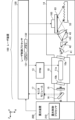
- FIG. 1 schematically shows the configuration of an exposure system in a comparative example.
- FIG. 2 schematically shows the configuration of the laser device.
- FIG. 3 is a diagram for explaining how the position of the scan field of the photosensitive substrate changes with respect to the position of the pulsed laser beam.
- FIG. 4 is a diagram for explaining how the position of the scan field of the photosensitive substrate changes with respect to the position of the pulsed laser beam.
- FIG. 5 is a diagram for explaining how the position of the scan field of the photosensitive substrate changes with respect to the position of the pulsed laser beam.
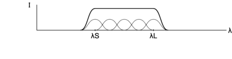
- FIG. 6 is a graph showing periodic wavelength changes.
- FIG. 7 shows an integrated spectrum of pulsed laser light containing a plurality of center wavelengths.
- FIG. 8 shows an example in which a wafer pattern different from the target pattern is formed due to the optical proximity effect when the target pattern is used as the mask pattern as it is.
- FIG. 9 shows an example in which a wafer pattern close to the target pattern is formed when a corrected mask pattern subjected to optical proximity correction is used.
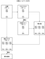
- FIG. 10 is a conceptual diagram of model-based OPC in a comparative example.
- FIG. 11 is a flowchart of model-based OPC.
- FIG. 12 shows the data structure of the measurement wafer pattern.
- FIG. 13 is a flow chart showing the details of the process of creating a model function group.
- FIG. 14 is a conceptual diagram of rule-based OPC in a comparative example.
- FIG. 15 is a flowchart of rule-based OPC.
- FIG. 16 shows the data structure of correction values.
- FIG. 17 shows the concept of off-axis chromatic aberration that occurs when a photosensitive substrate is exposed with pulsed laser light of multiple wavelengths.
- FIG. 18 is a conceptual diagram of split model-based OPC in the first embodiment.
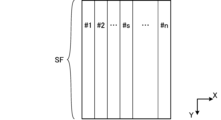
- FIG. 19 shows a plurality of segmented areas included in the scan field of the test wafer.
- FIG. 20 is a flowchart of split model-based OPC.
- FIG. 21 shows the data structure of the measurement wafer pattern.
- FIG. 22 is a flow chart showing the details of the process of creating a model function group.
- FIG. 23 shows an example of a model function group.
- FIG. 24 is a conceptual diagram of common model-based OPC in the second embodiment.
- FIG. 25 shows a plurality of segmented areas included in the scan field of the test wafer.
- FIG. 26 is a flowchart of common model-based OPC.
- FIG. 27 is a flow chart showing the details of the process of creating a model function group.
- FIG. 28 shows the data structure of the difference.
- FIG. 29 is a conceptual diagram of division rule-based OPC in the third embodiment.
- FIG. 30 is a flow chart of division rule-based OPC.
- FIG. 31 shows the data structure of correction values.
- FIG. 1 schematically shows the configuration of an exposure system in a comparative example.
- the comparative examples of the present disclosure are forms known by the applicant to be known only by the applicant, and not known examples to which the applicant admits.
- the exposure system includes a laser device 100 and an exposure device 200 .
- a laser device 100 is shown in simplified form in FIG.
- the laser device 100 includes a laser control processor 130 .
- the laser control processor 130 is a processing device that includes a memory 132 storing a control program and a CPU (central processing unit) 131 that executes the control program.
- Laser control processor 130 is specially configured or programmed to perform the various processes contained in this disclosure.
- the laser device 100 is configured to output pulsed laser light toward the exposure device 200 .
- the exposure apparatus 200 includes an illumination optical system 201, a projection optical system 202, and an exposure control processor 210. As shown in FIG.
- the illumination optical system 201 illuminates a mask pattern of a photomask (not shown) placed on the mask stage MS with pulsed laser light incident from the laser device 100 .
- the projection optical system 202 reduces and projects the pulsed laser beam that has passed through the photomask, and forms an image on a workpiece (not shown) placed on the workpiece table WT.
- the workpiece is a photosensitive substrate such as a semiconductor wafer coated with a resist film.
- the exposure control processor 210 is a processing device that includes a memory 212 storing control programs and a CPU 211 that executes the control programs. Exposure control processor 210 is specially configured or programmed to perform the various processes contained in this disclosure. The exposure control processor 210 supervises the control of the exposure apparatus 200 and transmits/receives various parameters and various signals to/from the laser control processor 130 .
- the exposure control processor 210 transmits various parameters including the target long wavelength ⁇ L, target short wavelength ⁇ S, and voltage command value, and a trigger signal to the laser control processor 130 .
- Laser control processor 130 controls laser device 100 according to these parameters and signals.
- Exposure control processor 210 synchronously translates mask stage MS and workpiece table WT in opposite directions. As a result, the workpiece is exposed to pulsed laser light that reflects the mask pattern. A mask pattern is transferred to a photosensitive substrate by such photolithography. After that, an electronic device can be manufactured through a plurality of steps.
- FIG. 2 schematically shows the configuration of the laser device 100. As shown in FIG. FIG. 2 shows V-, H-, and Z-axes that are perpendicular to each other. FIG. 2 shows the laser device 100 viewed in the -V direction, and the exposure device 200 is simplified.
- the laser device 100 includes a laser chamber 10 , a pulse power module (PPM) 13 , a band narrowing module 14 , an output coupling mirror 15 and a monitor module 17 in addition to the laser control processor 130 .
- the band narrowing module 14 and the output coupling mirror 15 constitute an optical resonator.
- a laser chamber 10 is arranged in the optical path of the optical resonator.
- a laser chamber 10 is provided with windows 10a and 10b.
- the laser chamber 10 internally includes a discharge electrode 11a and a discharge electrode (not shown) paired with the discharge electrode 11a.
- a discharge electrode (not shown) is positioned so as to overlap the discharge electrode 11a in the V-axis direction.
- the laser chamber 10 is filled with a laser gas containing, for example, argon gas or krypton gas as a rare gas, fluorine gas as a halogen gas, and neon gas as a buffer gas.
- the pulse power module 13 includes a switch (not shown) and is connected to a charger (not shown).
- Band narrowing module 14 includes prisms 41 - 43 , grating 53 and mirror 63 . Details of the band narrowing module 14 will be described later.
- the output coupling mirror 15 consists of a partially reflective mirror.
- a beam splitter 16 is arranged in the optical path of the pulsed laser light output from the output coupling mirror 15 to transmit part of the pulsed laser light with high transmittance and reflect the other part.
- a monitor module 17 is arranged in the optical path of the pulsed laser beam reflected by the beam splitter 16 .
- the laser control processor 130 acquires various parameters including the target long wavelength ⁇ L, the target short wavelength ⁇ S, and the voltage command value from the exposure control processor 210 .
- Laser control processor 130 sends a control signal to narrowband module 14 based on target long wavelength ⁇ L and target short wavelength ⁇ S.
- the laser control processor 130 receives trigger signals from the exposure control processor 210 .
- the laser control processor 130 transmits an oscillation trigger signal based on the trigger signal to the pulse power module 13 .
- a switch included in the pulse power module 13 is turned on when an oscillation trigger signal is received from the laser control processor 130 .
- the pulse power module 13 When the switch is turned on, the pulse power module 13 generates a pulsed high voltage from the electrical energy charged in the charger, and applies this high voltage to the discharge electrode 11a.
- discharge electrode 11a When a high voltage is applied to the discharge electrode 11a, discharge occurs in the discharge space between the discharge electrode 11a and a discharge electrode (not shown). The energy of this discharge excites the laser gas in the laser chamber 10 to shift to a high energy level. When the excited laser gas then shifts to a lower energy level, it emits light with a wavelength corresponding to the energy level difference.
- the light generated within the laser chamber 10 is emitted outside the laser chamber 10 through the windows 10a and 10b.
- Light emitted from the window 10 a enters the band narrowing module 14 .
- the band-narrowing module 14 Of the light incident on the band-narrowing module 14 , light near the desired wavelength is folded back by the band-narrowing module 14 and returned to the laser chamber 10 .
- the output coupling mirror 15 transmits and outputs part of the light emitted from the window 10 b and reflects the other part back to the laser chamber 10 .
- the monitor module 17 measures the central wavelength of the pulsed laser beam and transmits the measured wavelength to the laser control processor 130 .
- a laser control processor 130 feedback controls the band narrowing module 14 based on the measured wavelength.
- the pulsed laser light that has passed through the beam splitter 16 enters the exposure device 200 .
- the prisms 41 to 43 are arranged on the optical path of the light beam emitted from the window 10a in ascending order of their numbers.
- the prisms 41 to 43 are arranged so that the surfaces of the prisms 41 to 43 through which light beams enter and exit are all parallel to the V-axis.
- the prism 43 is rotatable around an axis parallel to the V-axis by a rotating stage 143 .
- the mirror 63 is arranged in the optical path of the light beams transmitted through the prisms 41-43.
- the mirror 63 is arranged so that the surface that reflects the light beam is parallel to the V-axis, and is rotatable around an axis parallel to the V-axis by a rotating stage 163 .
- the grating 53 is arranged in the optical path of the light beam reflected by the mirror 63.
- the direction of the grooves of the grating 53 is parallel to the V-axis.
- the light beam emitted from the window 10a is changed in direction by each of the prisms 41 to 43 in a plane parallel to the HZ plane, which is a plane perpendicular to the V axis, and becomes parallel to the HZ plane.
- the beam width can be expanded in the plane.
- the light beams transmitted through the prisms 41 to 43 are reflected by the mirror 63 and enter the grating 53 .
- a light beam incident on the grating 53 is reflected by the plurality of grooves of the grating 53 and diffracted in a direction according to the wavelength of the light.
- the grating 53 has a Littrow arrangement so that the incident angle of the light beam incident on the grating 53 from the mirror 63 and the diffraction angle of the diffracted light of the desired wavelength match.
- the mirror 63 and prisms 41-43 reduce the beam width of the light beam returned from the grating 53 in a plane parallel to the HZ plane, and return the light beam to the interior of the laser chamber 10 through the window 10a. .
- the laser control processor 130 controls the rotation stages 143 and 163 via drivers (not shown). Depending on the rotation angles of the rotation stages 143 and 163, the incident angle of the light beam incident on the grating 53 changes, and the wavelength selected by the band narrowing module 14 changes.
- Rotating stage 143 is mainly used for coarse adjustment
- rotating stage 163 is mainly used for fine adjustment.
- the laser control processor 130 controls the rotation stage 163 so that the attitude of the mirror 63 periodically changes for each pulse. .
- the central wavelength of the pulsed laser light periodically changes between the target long wavelength ⁇ L and the target short wavelength ⁇ S for every plurality of pulses.
- the laser device 100 can perform laser oscillation at multiple wavelengths.
- the focal length of the exposure apparatus 200 depends on the wavelength of the pulsed laser light.
- the pulsed laser light that is oscillated at a plurality of wavelengths and is incident on the exposure apparatus 200 can form images at a plurality of different positions in the direction of the optical path axis of the pulsed laser light, so that the depth of focus can be substantially increased. can. For example, even when a resist film having a large thickness is exposed, the imaging performance in the thickness direction of the resist film can be maintained. Alternatively, a resist profile representing the cross-sectional shape of the developed resist film can be adjusted.
- FIGS. 3 to 5 show how the position of the scan field SF of the photosensitive substrate changes with respect to the position of the pulsed laser beam.
- the photosensitive substrate is, for example, a plate of monocrystalline silicon having a substantially disk shape and is coated with, for example, a photosensitive resist film.
- the scan field SF is, for example, a region where some semiconductor chips out of a large number of semiconductor chips formed on the photosensitive substrate are formed, and the mask pattern of one mask is transferred by one scan. Corresponds to area.
- pulsed laser light is continuously output at a predetermined repetition frequency. Continuous output of pulsed laser light at a predetermined repetition frequency is called burst output.
- the output of the pulsed laser light is stopped. Therefore, the burst output is repeated multiple times to expose one photosensitive substrate.
- the width of the scan field SF in the X-axis direction corresponds to the width in the X-axis direction of the beam cross section B of the pulsed laser light at the position of the workpiece table WT (see FIG. 1).
- the width of the scan field SF in the Y-axis direction is larger than the width W in the Y-axis direction of the beam cross section B of the pulsed laser light at the position of the workpiece table WT.
- the procedure for scanning and exposing the scan field SF with the pulsed laser light is performed in the order of FIGS.
- the workpiece is positioned so that the +Y direction end SFy+ of the scan field SF is located at a predetermined distance in the ⁇ Y direction from the position of the ⁇ Y direction end By ⁇ of the beam cross section B.
- a table WT is positioned.
- the work piece table WT is accelerated in the +Y direction so that the +Y direction end SFy+ of the scan field SF coincides with the position of the ⁇ Y direction end By ⁇ of the beam cross section B so as to reach a velocity Vy. .
- FIG. 3 As shown in FIG.
- the scan field SF is exposed while moving the work piece table WT in the +Y direction so that the position of the scan field SF performs uniform linear motion at a velocity Vy with respect to the position of the beam cross section B. be.
- FIG. 5 when the workpiece table WT is moved until the -Y-direction end SFy- of the scan field SF passes the position of the +Y-direction end By+ of the beam cross-section B, scanning of the scan field SF is started. finish.
- F is the repetition frequency of the pulsed laser light.
- the irradiation pulse number Ns is also referred to as the N slit pulse number.
- FIG. 6 is a graph showing periodic wavelength change.
- the horizontal axis indicates time t
- the vertical axis indicates wavelength ⁇ .
- Each small circle shown in FIG. 6 indicates the time t when the pulsed laser light is output and the center wavelength at that time.
- the center wavelength changes periodically between the target long wavelength ⁇ L and the target short wavelength ⁇ S.
- N be the number of pulses for one period of wavelength change.
- FIG. 7 shows an integrated spectrum of pulsed laser light containing a plurality of central wavelengths.
- the integrated spectrum shown in FIG. 7 corresponds to the integrated spectrum for one cycle of wavelength change shown in FIG.
- the horizontal axis indicates the wavelength ⁇
- the vertical axis indicates the light intensity I.
- a dashed line indicates the spectrum of the pulsed laser light for each pulse, and the center wavelength of each line may match the peak wavelength.
- the irradiation pulse number Ns of the pulsed laser light irradiated to an arbitrary point in the scan field SF is a multiple of the pulse number N for one period of wavelength change.
- any portion of the scan field SF is irradiated with the pulsed laser light having the same integrated spectrum and the irradiation pulse number Ns.
- Optical Proximity Correction 1.6.1 Overview
- OPC optical proximity correction
- FIG. 8 shows an example in which a wafer pattern R1 different from the target pattern G is formed due to the optical proximity effect when the target pattern G is used as the mask pattern as it is.
- the corners included in the target pattern G may be rounded in the wafer pattern R1, and the convex portions included in the target pattern G may recede in the wafer pattern R1.
- FIG. 9 shows an example in which a wafer pattern R2 close to the target pattern G is formed when a corrected mask pattern F subjected to optical proximity correction is used.
- the correction mask pattern F may be, for example, adding an overhang to a convex corner of the target pattern G, further recessing a recessed corner of the target pattern G, or forming an auxiliary pattern SRAF (sub-resolution assist feature). Including modifications such as adding Thereby, a wafer pattern R2 having a shape close to the target pattern G can be obtained.
- optical proximity correction it is possible not only to correct the optical proximity effect, but also to correct the differences between the mask pattern and the wafer pattern that occur in resist film development and other semiconductor processes.
- model-based OPC and rule-based OPC. These are described below.
- Model-based OPC In model-based OPC, a model function group M is created based on the result of an exposure simulation performed for each characteristic shape included in the target pattern G and the actual exposure result. Using this model function group M, a correction mask pattern F for obtaining a wafer pattern equivalent to the target pattern G is created. Model-based OPC is mainly used in the sub-130 nm linewidth generation.
- FIG. 10 is a conceptual diagram of model-based OPC in a comparative example.
- a test mask including a test mask pattern E is created.
- a test wafer is exposed using a test mask, and the patterned test wafer is measured to obtain a measurement wafer pattern D.
- FIG. 10 is a conceptual diagram of model-based OPC in a comparative example.
- a model function group M for predicting the actual exposure result from the exposure simulation result is created based on the result of the exposure simulation using the test mask pattern E and the measurement wafer pattern D which is the actual exposure result. .
- an OPC recipe P which is a program for creating a correction mask pattern F from a target pattern G, is created.
- a correction mask pattern F is created.
- exposing the photosensitive substrate using the correction mask pattern F a wafer pattern close to the target pattern G can be obtained.
- FIG. 11 is a flowchart of model-based OPC. The processing shown in FIG. 11 is primarily performed by a processor such as the exposure control processor 210 .
- the processor may be included in another apparatus such as a mask manufacturing apparatus (not shown), and such a processor may have the same configuration as the exposure control processor 210 .
- the processor acquires the target pattern G.
- the target pattern G is a target wafer pattern of a photosensitive substrate designed by a semiconductor chip designer, and is provided in a data format called GDS (Graphic Data System), for example.
- GDS Graphic Data System
- the target pattern G may be a pattern after etching when the photosensitive substrate is etched, or may be a pattern of a resist film developed after exposure when etching is not performed.
- the processor sets exposure conditions based on the target pattern G.
- the exposure conditions include setting conditions of the exposure apparatus 200 , such as the shape of the illumination light source of the illumination optical system 201 (see FIG. 1), the presence or absence of polarized illumination, and the numerical aperture of the projection optical system 202 . Further, for example, the exposure conditions include the type of resist film, the presence or absence and type of antireflection film, resist stack information, film thickness of the resist film, application conditions of the resist film, and development conditions.
- the processor creates a test mask pattern E based on the target pattern G.
- FIG. Specifically, characteristic shapes included in the target pattern G are extracted, and the test mask pattern E is obtained by setting one or more dimension conditions for each shape. According to the test mask pattern E, a test mask is produced by a mask manufacturing apparatus.
- the exposure apparatus 200 exposes the test wafer by scanning the test wafer through the test mask.
- the test wafer is a test exposure substrate coated with a resist film under the same conditions as the photosensitive substrate. Furthermore, a developing device (not shown) develops the test wafer, and if etching is to be performed, an etching device (not shown) carries out etching, thereby patterning the test wafer.
- the processor measures the wafer pattern of the test wafer using a measuring device such as a CD-SEM (not shown) and acquires a measured wafer pattern D indicating the measurement result.
- FIG. 12 shows the data structure of the measurement wafer pattern D.
- the measurement wafer pattern D includes p dimensions measured for each of the m shapes 1 to m. For example, dimensions D 11 to D 1p are measured for shape 1, dimensions D 21 to D 2p are measured for shape 2, and dimensions D m1 to D mp are measured for shape m.
- the values of p in the shapes 1 to m may be different from each other, and the value of p may be 1 or 2 or more.
- the average value for each shape and each dimension is calculated from the measurement results in the plurality of scan fields SF, and the measurement wafer pattern D is obtained. do.
- the processor creates a model function group M based on the test mask pattern E and the measurement wafer pattern D.
- FIG. 13 is a flowchart showing the details of the process of creating the model function group M.
- the processing shown in FIG. 13 corresponds to the subroutine of S6 in FIG.
- the processor uses the test mask pattern E to perform exposure simulation with a single wavelength. Fourier imaging theory is used in the exposure simulation.
- the processor initializes the model function group M.
- the model function group M includes, for example, k functions M 1 to M k .
- Each of the functions M 1 -M k includes multiple coefficients.
- function M 1 includes i coefficients c 11 to c 1i
- function M k includes i coefficients c k1 to c ki .
- the values of i in the functions M 1 to M k may differ from each other.
- the processor applies the exposure simulation result to the model function group M to perform a wafer pattern prediction calculation.
- Prediction calculations include four arithmetic operations and convolution integrals.
- the processor determines whether or not the result of the prediction calculation matches the measured wafer pattern D. Even if the result of the prediction calculation does not completely match the measurement wafer pattern D, it can be determined that the result of the prediction calculation matches the measurement wafer pattern D if a predetermined condition is satisfied. If the result of the prediction calculation matches the measurement wafer pattern D (S66: YES), the processor regards the model function group M used in S65 as the created model function group M, and terminates the processing of this flowchart. Return to the process shown in 11. If the result of the prediction calculation does not match the measured wafer pattern D (S66: NO), the processor advances the process to S67.
- the processor updates the model function group M by changing the coefficients included in the model function group M and making other modifications.
- the updated model function group M includes, for example, k' functions M 1 to M k' .
- the value of k' indicating the number of functions M 1 to M k' may differ from the number of functions M 1 to M k included in the model function group M used in S65.
- the coefficients c' 11 to c' k'i included in the functions M 1 to M k' may also differ from the coefficients c 11 to c ki included in the model function group M used in S65.
- the processor After S67, the processor returns to S65 and updates the model function group M until the result of the prediction calculation matches the measured wafer pattern D.
- the processor creates an OPC recipe P based on the model function group M at S7.
- the OPC recipe P includes, for example, the definition of the model function group M, measurement points and measurement directions of dimensions D 11 to D mp shown in FIG. 12, and descriptions of mask pattern correction rules.
- the processor executes the OPC recipe P using the target pattern G to create a corrected mask pattern F.
- the correction mask pattern F is also provided in the GDS data format.
- the mask manufacturing apparatus creates a photomask based on the correction mask pattern F, and the processing of this flowchart ends.
- Rule-based OPC In the rule-based OPC, correction rules are determined in advance according to the dimensions of the shapes included in the target pattern G and the distances from other shapes, and a correction mask pattern F is created from the target pattern G according to the rules. .
- the rule-based OPC has a small amount of calculation and enables high-speed processing, but its accuracy is lower than that of the model-based OPC, and is mainly used in the line width generation up to around 130 nm.
- FIG. 14 is a conceptual diagram of rule-based OPC in a comparative example. It is the same as model-based OPC in that a test wafer is exposed using a test mask including a test mask pattern E created based on a target pattern G, and the patterned test wafer is measured to obtain a measured wafer pattern D. be.
- the correction value H is calculated based on the deviation amount of the measurement wafer pattern D, which is the actual exposure result with respect to the test mask pattern E.
- the correction value H is not necessarily a simple difference between the test mask pattern E and the measurement wafer pattern D. However, here, in order to make it conceptually easy to understand, the difference between the test mask pattern E and the measurement wafer pattern D is A correction value H is used.
- a correction mask pattern F is created by adding a correction value H to the target pattern G. By exposing the photosensitive substrate using the correction mask pattern F, a wafer pattern close to the target pattern G can be obtained.
- FIG. 15 is a flowchart of rule-based OPC.
- the processing shown in FIG. 15 is mainly performed by a processor.
- the processing from S1 to S5 and S11 is the same as the processing in model-based OPC described with reference to FIG.
- the processor calculates a correction value H based on the amount of deviation between the test mask pattern E and the measurement wafer pattern D.
- FIG. 16 shows the data structure of the correction value H.
- the correction value H includes correction values corresponding to p dimensions measured for each of the m shapes 1 to m. For example, correction values H 11 to H 1p are calculated for shape 1, correction values H 21 to H 2p are calculated for shape 2, and correction values H m1 to H mp are calculated for shape m.
- the values of p in the shapes 1 to m may be different from each other, and the value of p may be 1 or 2 or more.
- rule-based OPC is similar to model-based OPC.
- FIG. 17 shows the concept of off-axis chromatic aberration CA that occurs when a photosensitive substrate is exposed with pulsed laser beams of multiple wavelengths.
- the refractive index in the projection optical system 202 differs between the target long wavelength ⁇ L and the target short wavelength ⁇ S
- the optical path of the projection optical system 202 in the mask pattern of the mask placed on the mask stage MS is The portion lying on the axis A is imaged at different positions in the depth direction of the photosensitive substrate placed on the workpiece table WT. This is called axial chromatic aberration.
- a portion of the mask pattern located away from the optical path axis A forms an image at a different position not only in the depth direction of the photosensitive substrate but also in the surface direction of the photosensitive substrate. This is called off-axis chromatic aberration CA.
- FIG. 18 is a conceptual diagram of split model-based OPC in the first embodiment.
- each of target pattern G, test mask pattern E, measurement wafer pattern D, model function group M, OPC recipe P, and correction mask pattern F is created for each of a plurality of divided regions #1 to #n.
- FIG. 19 shows a plurality of divided areas #1 to #n included in the scan field SF of the test wafer.
- n is an integer of 2 or more, and a plurality of divided regions #1, #2, . . . , and #n are arranged in this order.
- the slit direction is, for example, the X-axis direction perpendicular to the -Y direction and corresponds to the second direction in the present disclosure. It is desirable that the divided regions #1 to #n have the same width in the slit direction.
- the number of divided regions #1 to #n, that is, the value of n is desirably 3 or more and 15 or less.
- the measurement wafer pattern D obtained from the scan field SF of the test wafer is divided into measurement wafer patterns D#1 to D#n corresponding to the divided regions #1 to #n.
- a single scan field SF included in the test wafer corresponds to an area in which a test mask pattern E formed on a single test mask is transferred in one scan, and has a corresponding relationship with the test mask.
- the test mask pattern E is also divided into test mask patterns E#1 to E#n corresponding to the divided regions #1 to #n.
- One scan field SF included in the test wafer has a corresponding relationship with one scan field SF included in the photosensitive substrate.
- a target pattern G to be formed on the photosensitive substrate is also divided into target patterns G#1 to G#n corresponding to the divided areas #1 to #n.
- a single scan field SF included in the photosensitive substrate corresponds to a region in which the correction mask pattern F of one photomask is transferred by one scan, and has a corresponding relationship with the photomask.
- Correction mask pattern F is also divided into correction mask patterns F#1 to F#n corresponding to divided regions #1 to #n.
- model function groups M#1 to M#n corresponding to divided regions #1 to #n are created, and OPC recipes P#1 to P#n corresponding to divided regions #1 to #n are prepared. is created.
- One of the divided regions #1 to #n in the first embodiment corresponds to the first divided region in this disclosure, and the other one corresponds to the second divided region in this disclosure.
- measurement wafer pattern D#1 corresponds to the first measurement wafer pattern in the present disclosure
- the test mask pattern E#1 corresponds to the first test mask pattern in the present disclosure
- the target pattern G#1 corresponds to the first target pattern in the present disclosure
- the correction mask pattern F#1 corresponds to the first test mask pattern in the present disclosure
- the model function group M#1 corresponds to the first model function in the present disclosure.
- measurement wafer pattern D#2 corresponds to the second measurement wafer pattern in the present disclosure
- test mask pattern E#2 corresponds to the second measurement wafer pattern in the present disclosure
- target pattern G#2 corresponds to the second target pattern in the present disclosure
- correction mask pattern F#2 corresponds to the second correction mask pattern in the present disclosure
- model Function group M#2 corresponds to the second model function in the present disclosure.
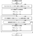
- FIG. 20 is a flowchart of split model-based OPC. The processing shown in FIG. 20 is mainly performed by a processor such as the exposure control processor 210. FIG.
- the processor acquires target patterns G#1 to G#n.
- target patterns G#1 to G#n are obtained by dividing a target pattern G designed by a semiconductor chip designer into divided regions #1 to #n.
- the processing of S2 is the same as the processing in model-based OPC described with reference to FIG.
- the processor creates test mask patterns E#1 to E#n based on the target patterns G#1 to G#n. For example, a test mask pattern E#1 is created based on the characteristic shape included in the target pattern G#1, and a test mask pattern E#2 is created based on the characteristic shape included in the target pattern G#2. , and so on, different test mask patterns E#1 to E#n may be created for the divided regions #1 to #n. Alternatively, based on the characteristic shapes included in the target patterns G#1 to G#n, common test mask patterns, that is, test mask patterns E#1 to E#n including the same pattern shapes are created. good too. A test mask is produced by the mask manufacturing apparatus according to the test mask patterns E#1 to E#n.
- the exposure apparatus 200 exposes the test wafer by scanning the test wafer through the test mask. Exposure of the test wafer is performed with multiple wavelengths of light used to expose the photosensitive substrate. Furthermore, a developing device (not shown) develops the test wafer, and if etching is to be performed, an etching device (not shown) carries out etching, thereby patterning the test wafer.
- the processor measures the wafer pattern of the test wafer and acquires measurement wafer patterns D#1-D#n indicating the measurement results in the plurality of divided regions #1-#n.
- FIG. 21 shows the data structure of the measurement wafer patterns D#1 to D#n.
- Each of the measurement wafer patterns D#1-D#n includes p dimensions measured for each of the m shapes 1-m.
- model function groups M#1 to M#n based on test mask patterns E#1 to E#n and measurement wafer patterns D#1 to D#n, respectively. do.
- model function group M#1 is created based on test mask pattern E#1 and measurement wafer pattern D#1
- model function group M#2 is created based on test mask pattern E#2 and measurement wafer pattern D#2.
- FIG. 22 is a flowchart showing the details of the process of creating the model function groups M#1 to M#n. The processing shown in FIG. 22 corresponds to the subroutine of S6a in FIG.
- the processor performs exposure simulation using the test mask patterns E#1 to E#n.
- the exposure simulation may be performed using light having a smaller number of center wavelengths than the pulsed laser light containing a plurality of center wavelengths obtained by scanning the test wafer. It is desirable to perform the exposure simulation at a single wavelength.
- the value of the counter j is set to the initial value 1.
- a counter j specifies one of the model function groups M#1 to M#n and one of the test mask patterns E#1 to E#n and one of the measurement wafer patterns D#1 to D#n. Identify.
- the processing of S64a to S67a is the same as the processing of S64 to S67 described with reference to FIG.
- the exposure simulation result using one of the test mask patterns E#1 to E#n specified by the counter j and one of the measurement wafer patterns D#1 to D#n specified by the counter j are is used to create one of the model function group M#1-M#n specified by the counter j.
- the processor proceeds to S68a.
- the processor determines whether the value of the counter j is greater than or equal to n. If the value of the counter j is less than n (S68a: NO), the processor adds 1 to the value of the counter j in S69a, returns the process to S64a, and sets the model function group M#j for another divided region. do. If the value of the counter j is greater than or equal to n, the processor ends the processing of this flowchart and returns to the processing shown in FIG.
- FIG. 23 shows an example of model function groups M#1 to M#n.
- one model function group M#j includes k functions M#j 1 to M#j k .
- the number of functions M#j 1 to M#j k that is, the value of k may be different in the model function group M#1 to M#n.
- the processor creates OPC recipes P#1 to P#n based on the model function groups M#1 to M#n, respectively.
- the processor executes the OPC recipes P#1 to P#n using the target patterns G#1 to G#n, respectively, to create correction mask patterns F#1 to F#n, respectively.
- a corrected mask pattern F#1 is created based on the target pattern G#1 and the model function group M#1
- a corrected mask pattern F# is created based on the target pattern G#2 and the model function group M#2. 2 is created.
- the mask manufacturing apparatus creates photomasks based on the correction mask patterns F#1 to F#n, and the processing of this flowchart ends.
- a pulsed laser beam containing a plurality of central wavelengths is applied to a test wafer in the -Y direction through a test mask. Scan to pattern the test wafer. Also, a wafer pattern of a patterned test wafer is measured, and a measurement wafer pattern D showing measurement results in each of a plurality of divided regions #1 to #n arranged in a slit direction intersecting the -Y direction on the surface of the test wafer. #1 to D#n are acquired.
- test mask patterns E#1 to E#n are generated based on test mask patterns E#1 to E#n and measurement wafer patterns D#1 to D#n.
- model function groups M#1 to M#n for predicting the measured wafer patterns D#1 to D#n are created.
- correction mask patterns F#1 to F#n are created based on the target patterns G#1 to G#n and the model function group M#1 to M#n. According to this, by using the model function, highly accurate optical proximity correction can be performed to create the corrected mask patterns F#1 to F#n.
- the test mask patterns E#1 to E#n are used to scan the test wafer, and the light having a smaller number of center wavelengths than the pulsed laser light containing a plurality of center wavelengths is used.
- An exposure simulation is performed to create a model function group M#1 to M#n.
- off-axis chromatic aberration is reflected in the measurement wafer patterns D#1 to D#n by scanning the test wafer with pulsed laser light containing a plurality of center wavelengths. Therefore, in the exposure simulation for creating the model function groups M#1 to M#n, the number of center wavelengths can be reduced to reduce the calculation load.
- a plurality of model function groups M#1 to M#n are created for each of the plurality of divided regions #1 to #n.
- the optical proximity correction can be performed in consideration of the off-axis chromatic aberration in the slit direction for each divided region.
- the amount of calculation for creating the model function groups M#1 to M#n depends on the areas of the test mask and test wafer. Even when the model function groups M#1 to M#n are created for each divided region, the area of the test mask and the test wafer does not change, so the computational complexity is the same as when creating the model function group M in the comparative example.
- the measurement wafer patterns D#1 to D#n are the first measurement wafer patterns in the first divided region #1 of the plurality of divided regions #1 to #n. D#1, and a second measurement wafer pattern D#2 in a second divided area #2 of the plurality of divided areas #1 to #n.
- the test mask patterns E#1 to E#n are the first test mask pattern E#1 in the portion corresponding to the first divided region #1 of the test mask and the second divided region of the test mask. and a second test mask pattern E#2 in the portion corresponding to #2.
- the model function group M#1 to M#n are a first model function group M#1 created for the first divided area #1 and a second model function created for the second divided area #2. and a group M#2.
- a first model function group M#1 is created, and a second test mask pattern E#2 and , a second measurement wafer pattern D#2, and a second model function group M#2.
- the first model function group M#1 is created using the first test mask pattern E#1 and the first measurement wafer pattern D#1 corresponding to the first divided area #1
- the second model function group M#2 is created using the second test mask pattern E#2 and the second measurement wafer pattern D#2 corresponding to the second divided area #2.
- the first test mask pattern E#1 and the second test mask pattern E#2 include the same pattern shape. This facilitates the manufacture of test masks and the measurement of test wafers, thus facilitating the handling of data.
- the plurality of segmented regions #1 to #n include first and second segmented regions #1 and #2.
- the target patterns G#1 to G#n are the first target pattern G#1 in the portion of the photosensitive substrate corresponding to the first divided region #1 and the second divided region #2 of the photosensitive substrate. and the second target pattern G#2 in the portion corresponding to .
- the correction mask patterns F#1 to F#n are the first correction mask pattern F#1 in the portion of the photomask corresponding to the first division region #1, and the second division region of the photomask. and a second correction mask pattern F#2 in the portion corresponding to #2.
- a first corrected mask pattern F#1 is created, and a second target pattern G#2 and A second correction mask pattern F#2 is created based on the second model function group M#2.
- First and second corrected mask patterns F#1 and F#2 can be created by performing optical proximity correction that takes chromatic aberration into account.
- the first embodiment is the same as the model-based OPC in the comparative example.
- FIG. 24 is a conceptual diagram of common model-based OPC in the second embodiment.
- Common model-based OPC differs from the divided model in the first embodiment in that the number of model function groups M#s and the number of OPC recipes P#s to be created are smaller than the number n of divided regions #1 to #n. Different from base OPC.
- the number of model function groups M#s and the number of OPC recipes P#s to be created may be one.
- FIG. 25 shows a plurality of divided areas #1 to #n included in the scan field SF of the test wafer.
- Segmented regions #1 to #n include segmented region #s.
- s is an integer greater than or equal to 1 and less than or equal to n.
- the divided region #s is referred to as the first divided region #s, and the divided regions #1 to #(s ⁇ 1) and #(s+1) to #n other than the first divided region #s is sometimes referred to as a second divided area.
- the first divided area #s is preferably closer to the center of the scan field SF in the slit direction than the second divided areas #1 to #(s ⁇ 1) and #(s+1) to #n. For example, if n is an odd number, s may be (n+1)/2 and the first divided region #s may be positioned at the center of the scan field SF.
- model function group M#s is created based on the test mask pattern E#s in the first divided area #s and the measurement wafer pattern D#s in the first divided area #s. be done.
- An OPC recipe P#s is created based on the model function group M#s.
- Differences ⁇ #1 to ⁇ #n between measurement wafer patterns D#1 to D#n and measurement wafer pattern D#s are calculated, and target patterns G#1 to G#1 to G are calculated based on the differences ⁇ #1 to ⁇ #n.
- Correction target patterns GB#1 to GB#n are created by correcting #n.
- Correction mask patterns F#1 to F#n are created by executing OPC recipe P#s using correction target patterns GB#1 to GB#n. However, since the corrected target pattern GB#s is the same as the target pattern G#s, executing the OPC recipe P#s using the corrected target pattern GB#s is equivalent to executing the OPC recipe P#s using the target pattern G#s. Equivalent to executing P#s.
- the measurement wafer pattern D#s in the second embodiment corresponds to the first measurement wafer pattern in the present disclosure
- measurement wafer patterns D#1 to D#(s ⁇ 1) and D#(s+1) to D#n corresponds to the second measurement wafer pattern in the present disclosure
- Test mask pattern E#s in the second embodiment corresponds to the first test mask pattern in the present disclosure
- test mask patterns E#1 to E#(s ⁇ 1) and E#(s+1) to E#n corresponds to the second test mask pattern in the present disclosure
- the target pattern G#s in the second embodiment corresponds to the first target pattern in the present disclosure, and is one of the target patterns G#1 to G#(s ⁇ 1) and G#(s+1) to G#n. corresponds to the second target pattern in the present disclosure.
- Correction mask pattern F#s in the second embodiment corresponds to the first correction mask pattern in the present disclosure
- correction mask patterns F#1 to F#(s ⁇ 1) and F#(s+1) to F#n corresponds to the second correction mask pattern in the present disclosure
- FIG. 26 is a flowchart of common model-based OPC. The processing shown in FIG. 26 is mainly performed by a processor such as the exposure control processor 210. FIG.
- test mask patterns E#1 to E#n desirably include the same pattern, but they do not necessarily have to include the same pattern. Since the test mask patterns E#1 to E#n include the same patterns, the differences ⁇ #1 to ⁇ #n between the measurement wafer patterns D#1 to D#n and the measurement wafer pattern D#s are used as they are. The differences resulting from external chromatic aberration can be used to create correction target patterns GB#1 to GB#n. If the test mask patterns E#1 to E#n do not include the same pattern, a process of extracting the portion caused by the off-axis chromatic aberration from the differences ⁇ #1 to ⁇ #n is performed.
- the processor creates a model function group M#s common to the divided regions #1 to #n based on the test mask pattern E#s and the measurement wafer pattern D#s.
- FIG. 27 is a flowchart showing the details of the process of creating the model function group M#s. The processing shown in FIG. 27 corresponds to the subroutine of S6b in FIG.
- the processor determines the measurement wafer patterns D#1 to D#n of the first divided area #s located at or near the center of the scan field SF in the slit direction and the divided areas #1 to #n. Differences ⁇ #1 to ⁇ #n are calculated.
- FIG. 28 shows the data structure of the differences ⁇ #1 to ⁇ #n.
- Each of the differences ⁇ #1 to ⁇ #n includes differences corresponding to p dimensions measured for each of the m shapes 1 to m.
- the difference ⁇ #1 includes the differences ⁇ #1 11 to ⁇ #1 mp
- the difference ⁇ #2 includes the differences ⁇ #2 11 to ⁇ #2 mp
- the difference ⁇ #n includes the differences ⁇ #n 11 to ⁇ Contains #nmp .
- the differences ⁇ #s 11 to ⁇ #s mp included in the difference ⁇ #s are all 0 although not shown.
- the processor inputs the differences ⁇ #1 to ⁇ #n as biases to the target patterns G#1 to G#n, respectively, thereby obtaining the corrected target patterns GB#1 to GB#n. to create
- the processing from S62b to S67b is the same as the processing from S62 to S67 described with reference to FIG.
- a common model function group M#s is created using the exposure simulation result using the test mask pattern E#s and the measurement wafer pattern D#s. Measurement wafer patterns D#1 to D#(s ⁇ 1) and D#(s+1) to D#n other than measurement wafer pattern D#s do not have to be used for creating a model function group.
- the processor ends the processing of this flowchart and returns to the processing shown in FIG.
- the processor creates an OPC recipe P#s common to the divided regions #1 to #n based on the model function group M#s.
- the processor executes the OPC recipe P#s using the correction target patterns GB#1 to GB#n to create correction mask patterns F#1 to F#n, respectively.
- the processing of S11a is the same as the division model-based OPC processing described with reference to FIG. After S11a, the processing of this flowchart is terminated.
- the measurement wafer patterns D#1 to D#n are the first patterns in the first divided region #s among the plurality of divided regions #1 to #n. and the second measurement wafer pattern in the second divided regions #1 to #(s ⁇ 1) and #(s+1) to #n among the plurality of divided regions #1 to #n D#1 to D#(s ⁇ 1) and D#(s+1) to D#n. Differences ⁇ #1 to ⁇ # between the first measurement wafer pattern D#s and the second measurement wafer patterns D#1 to D#(s ⁇ 1) and D#(s+1) to D#n (s ⁇ 1) and ⁇ #(s+1) to ⁇ #n are calculated.
- the target patterns G#1 to G#n are corrected to correct the corrected target patterns GB#1 to GB#n.
- correction mask patterns F#1 to F#n are created based on the correction target patterns GB#1 to GB#n and the model function group M#s.
- the difference ⁇ #1 between the first measurement wafer pattern D#s and the second measurement wafer patterns D#1 to D#(s ⁇ 1) and D#(s+1) to D#n ⁇ #(s ⁇ 1) and ⁇ #(s+1) ⁇ #n are used to create correction target patterns GB#1 to GB#n. It can reduce computational load.
- the first segmented region #s uses the test mask pattern E more than the second segmented regions #1 to #(s ⁇ 1) and #(s+1) to #n.
- #1 to E#n are close to the center in the slit direction of the scan field SF transferred by one scan.
- the test mask patterns E#1 to E#n are the first test mask pattern E#s in the portion corresponding to the first divided region #s of the test mask and the second divided region of the test mask.
- a model function group M#s is created based on the first test mask pattern E#s and the first measurement wafer pattern D#s. Since the influence of off-axis chromatic aberration in the slit direction is small in the first segmented region #s near the center of the scan field SF, the model function group M#s is created with the first segmented region #s as a reference, and the light Accuracy of proximity effect correction can be ensured.
- the off-axis chromatic aberration is calculated as differences ⁇ #1 to ⁇ #(s ⁇ 1) and ⁇ #(s+1) to ⁇ #n. can reduce the calculation load of the optical proximity correction considering the off-axis chromatic aberration in the slit direction.
- the target patterns G#1 to G#n are the first target pattern G#s in the portion of the photosensitive substrate corresponding to the first divided region #s, Second target patterns G#1 to G#(s ⁇ 1) and G in portions corresponding to second divided regions #1 to #(s ⁇ 1) and #(s+1) to #n of the photosensitive substrate #(s+1) to G#n.
- the correction mask patterns F#1 to F#n are the first correction mask pattern F#s in the portion of the photomask corresponding to the first division region #s, and the second division region of the photomask.
- Second target patterns G#1 to G#(s ⁇ 1) and G#(s+1) to G#n, model function group M#s, measurement wafer patterns D#1 to D#n, , the second correction mask patterns F#1 to F#(s ⁇ 1) and F#(s+1) to F#n are created. According to this, using one model function group M#s, the first correction mask pattern F#s, the second correction mask patterns F#1 to F#(s ⁇ 1) and F#(s+1 ) to F#n, the calculation load of the model function can be reduced. Also, the description for creating the OPC recipe P#s can be simplified.
- the first measurement wafer pattern D#s and the second measurement wafer patterns D#1 to D#(s ⁇ 1) and D#(s+1) to D#n , and the differences ⁇ #1 to ⁇ #(s ⁇ 1) and ⁇ #(s+1) to ⁇ #n are calculated. Further, differences ⁇ #1 to ⁇ #(s ⁇ 1) and ⁇ #(s+1) to ⁇ #n, and second target patterns G#1 to G#(s ⁇ 1) and G#(s+1) to G #n and the model function group M#s, the second correction mask patterns F#1 to F#(s ⁇ 1) and F#(s+1) to F#n are created. According to this, second correction mask patterns F#1 to F#(s ⁇ 1) and F# Since (s+1) to F#n are generated and the calculation load of the model function can be reduced, the calculation load of the correction mask patterns F#1 to F#n can be reduced.
- second target patterns G#1 to G#(s ⁇ 1) and G#(s+1) to G# are generated based on measurement wafer patterns D#1 to D#n. n is corrected to create corrected target patterns GB#1 to GB#(s ⁇ 1) and GB#(s+1) to GB#n. Further, second correction mask patterns F#1 to Create F#(s ⁇ 1) and F#(s+1) to F#n. According to this, the second correction mask patterns F#1 to F#(s ⁇ 1) and Since F#(s+1) to F#n can be created to reduce the calculation load of the model function, the calculation load of the correction mask patterns F#1 to F#n can be reduced.
- the first test mask pattern E#s and the second test mask patterns E#1 to E#(s ⁇ 1) and E#(s+1) to E#n contain the same pattern shape. According to this, the influence of the off-axis chromatic aberration can be evaluated by the differences ⁇ #1 to ⁇ #(s ⁇ 1) and ⁇ #(s+1) to ⁇ #n, and the correction mask patterns F#1 to F#n can reduce the computational load of
- the first segmented region #s has the test mask pattern E more than the second segmented regions #1 to #(s ⁇ 1) and #(s+1) to #n.
- #1 to E#n are close to the center in the slit direction of the scan field SF transferred by one scan.
- the influence of off-axis chromatic aberration in the slit direction is small in the first divided region #s near the center of the scan field SF.
- a first correction mask pattern F#s and second correction mask patterns F#1 to F#(s ⁇ 1) are obtained using a model function group M#s created with reference to the first divided region #s. and F#(s+1) to F#n, the accuracy of optical proximity correction can be ensured.
- the second embodiment is the same as the first embodiment.
- FIG. 29 is a conceptual diagram of division rule-based OPC in the third embodiment.
- each of a target pattern G, a test mask pattern E, a measurement wafer pattern D, a correction value H, and a correction mask pattern F is created for each of a plurality of division regions #1 to #n.
- the divided areas #1 to #n are as explained with reference to FIG.
- a measurement wafer pattern D obtained from the scan field SF of the test wafer is divided into measurement wafer patterns D#1 to D#n corresponding to the divided areas #1 to #n.
- the test mask pattern E is also divided into test mask patterns E#1 to E#n corresponding to the divided regions #1 to #n.
- the target pattern G is also divided into target patterns G#1 to G#n corresponding to the divided regions #1 to #n.
- Correction mask pattern F is also divided into correction mask patterns F#1 to F#n corresponding to divided regions #1 to #n.
- correction values H#1 to H#n corresponding to division areas #1 to #n are calculated.
- One of the divided regions #1 to #n in the third embodiment corresponds to the first divided region in this disclosure, and the other one corresponds to the second divided region in this disclosure.
- measurement wafer pattern D#1 corresponds to the first measurement wafer pattern in the present disclosure
- the test mask pattern E#1 corresponds to the first test mask pattern in the present disclosure
- the target pattern G#1 corresponds to the first target pattern in the present disclosure
- the correction mask pattern F#1 corresponds to the first test mask pattern in the present disclosure.
- the correction value H#1 corresponds to the first correction value in the present disclosure.
- measurement wafer pattern D#2 corresponds to the second measurement wafer pattern in the present disclosure
- test mask pattern E#2 corresponds to the second measurement wafer pattern in the present disclosure
- target pattern G#2 corresponds to the second target pattern in the present disclosure
- correction mask pattern F#2 corresponds to the second correction mask pattern in the present disclosure
- correction The value H#2 corresponds to the second correction value in the present disclosure.
- FIG. 30 is a flow chart of division rule-based OPC.
- the processing shown in FIG. 30 is mainly performed by a processor such as the exposure control processor 210.
- FIG. The processing from S1a to S5a and S11a is the same as the division model-based OPC processing described with reference to FIG.
- the processor calculates correction values H#1 to H#n based on the amount of deviation between the test mask patterns E#1 to E#n and the measurement wafer patterns D#1 to D#n. .
- the correction value H#1 is calculated based on the amount of deviation between the test mask pattern E#1 and the measurement wafer pattern D#1, and based on the amount of deviation between the test mask pattern E#2 and the measurement wafer pattern D#2. to calculate the correction value H#2.
- FIG. 31 shows the data structure of the correction values H#1 to H#n.
- Each of the correction values H#1-H#n includes correction values for the p dimensions measured for each of the m shapes 1-m.
- the correction value H#1 includes the correction values H#1 11 to H#1 mp
- the correction value H#2 includes the correction values H#2 11 to H#2 mp
- the correction value H#n is the correction value Includes H#n 11 to H#n mp .
- the processor adds correction values H#1 to H#n to target patterns G#1 to G#n, respectively, to create corrected mask patterns F#1 to F#n. do.
- a correction mask pattern F#1 is created based on the target pattern G#1 and the correction value H#1
- a correction mask pattern F#2 is created based on the target pattern G#2 and the correction value H#2.
- the correction value H# 1 to H#n are calculated.
- correction mask patterns F#1 to F#n are created based on the target patterns G#1 to G#n and the correction values H#1 to H#n.
- the correction values H#1 to H#n based on the measurement results in each of the divided regions #1 to #n, it is possible to correct the optical proximity effect in consideration of the off-axis chromatic aberration in the slit direction with a simple calculation. can be executed to create correction mask patterns F#1 to F#n.
- a plurality of correction values H#1 to H#n are calculated for each of the plurality of divided regions #1 to #n. According to this, by calculating the correction values H#1 to H#n for the divided areas #1 to #n, respectively, the optical proximity effect correction can be performed in consideration of the off-axis chromatic aberration in the slit direction for each divided area. Correction mask patterns F#1 to F#n can be created.
- the measurement wafer patterns D#1 to D#n are the first measurement wafer patterns in the first divided region #1 of the plurality of divided regions #1 to #n. D#1, and a second measurement wafer pattern D#2 in a second divided area #2 of the plurality of divided areas #1 to #n.
- the test mask patterns E#1 to E#n are the first test mask pattern E#1 in the portion corresponding to the first divided region #1 of the test mask and the second divided region of the test mask. and a second test mask pattern E#2 in the portion corresponding to #2.
- the target patterns G#1 to G#n are the first target pattern G#1 in the portion of the photosensitive substrate corresponding to the first divided region #1 and the second divided region #2 of the photosensitive substrate.
- the correction mask patterns F#1 to F#n are the first correction mask pattern F#1 in the portion of the photomask corresponding to the first division region #1, and the second division region of the photomask. and a second correction mask pattern F#2 in the portion corresponding to #2. Also, a first correction value H#1 is calculated based on the amount of deviation between the first test mask pattern E#1 and the first measurement wafer pattern D#1, and a second test mask pattern E# is calculated. 2 and the second measurement wafer pattern D#2, a second correction value H#2 is calculated.
- a first correction mask pattern F#1 is created, and a second target pattern G#2 and a second mask pattern F#1 are created.
- a second correction mask pattern F#2 is created based on the correction value H#2 of 2.
- the first correction value H#1 is calculated using the first test mask pattern E#1 and the first measurement wafer pattern D#1 corresponding to the first divided region #1, and the first correction value H#1 is calculated.
- the first test mask pattern E#1 and the second test mask pattern E#2 include the same pattern shape. This facilitates the manufacture of test masks and the measurement of test wafers, thus facilitating the handling of data. Otherwise, the third embodiment is the same as the rule-based OPC in the comparative example.
Landscapes
- Physics & Mathematics (AREA)
- General Physics & Mathematics (AREA)
- Exposure And Positioning Against Photoresist Photosensitive Materials (AREA)
Abstract
The present invention provides an optical proximity effect correction method that takes into account the impact of off-axis chromatic aberration, which is generated in a case where a photosensitive substrate is exposed to pulse laser light including a plurality of center wavelengths. A photomask creation method includes: scanning, in a first direction and via a test mask, a test wafer by using pulse laser light, to pattern the test wafer (S2, S3a, S4a); measuring a wafer pattern of the patterned test wafer and acquiring a measured wafer pattern indicating the measurement result for each of a plurality of segmentation regions standing in a line in a second direction intersecting a first direction on the surface of the test wafer (S5a); creating a corrected mask pattern for creating a photomask on the basis of a test mask pattern formed on the test mask, the measured wafer pattern, and a target pattern which is a wafer pattern serving as a target for a photosensitive substrate (S6a, S7a, S8a); and creating the photomask on the basis of the corrected mask pattern (S11a).
Description
本開示は、フォトマスクの作成方法、データ作成方法、及び電子デバイスの製造方法に関する。
The present disclosure relates to a method of creating a photomask, a method of creating data, and a method of manufacturing an electronic device.
近年、半導体露光装置においては、半導体集積回路の微細化及び高集積化につれて、解像力の向上が要請されている。このため、露光用光源から放出される光の短波長化が進められている。例えば、露光用のガスレーザ装置としては、波長約248nmのレーザ光を出力するKrFエキシマレーザ装置、ならびに波長約193nmのレーザ光を出力するArFエキシマレーザ装置が用いられる。
In recent years, semiconductor exposure apparatuses have been required to improve their resolution as semiconductor integrated circuits have become finer and more highly integrated. For this reason, efforts are being made to shorten the wavelength of the light emitted from the exposure light source. For example, as gas laser devices for exposure, a KrF excimer laser device that outputs laser light with a wavelength of about 248 nm and an ArF excimer laser device that outputs laser light with a wavelength of about 193 nm are used.
KrFエキシマレーザ装置及びArFエキシマレーザ装置の自然発振光のスペクトル線幅は、350~400pmと広い。そのため、KrF及びArFレーザ光のような紫外線を透過させる材料で投影レンズを構成すると、色収差が発生してしまう場合がある。その結果、解像力が低下し得る。そこで、ガスレーザ装置から出力されるレーザ光のスペクトル線幅を、色収差が無視できる程度となるまで狭帯域化する必要がある。そのため、ガスレーザ装置のレーザ共振器内には、スペクトル線幅を狭帯域化するために、狭帯域化素子(エタロンやグレーティング等)を含む狭帯域化モジュール(Line Narrowing Module:LNM)が備えられる場合がある。スペクトル線幅が狭帯域化されるガスレーザ装置を狭帯域化レーザ装置という。
The spectral line width of the spontaneous oscillation light of the KrF excimer laser device and the ArF excimer laser device is as wide as 350-400 pm. Therefore, if the projection lens is made of a material that transmits ultraviolet light, such as KrF and ArF laser light, chromatic aberration may occur. As a result, resolution can be reduced. Therefore, it is necessary to narrow the spectral line width of the laser light output from the gas laser device to such an extent that the chromatic aberration can be ignored. Therefore, in the laser resonator of the gas laser device, a line narrowing module (LNM) including a band narrowing element (etalon, grating, etc.) is provided in order to narrow the spectral line width. There is A gas laser device whose spectral line width is narrowed is called a band-narrowed laser device.
本開示の1つの観点において、複数の中心波長が含まれるパルスレーザ光を用いたフォトリソグラフィに使用されるフォトマスクの作成方法は、テストマスクを介してパルスレーザ光でテストウエハを第1の方向にスキャンして、テストウエハをパターニングすることと、パターニングされたテストウエハのウエハパターンを計測し、テストウエハの面上で第1の方向と交差する第2の方向に並ぶ複数の分割領域の各々における計測結果を示す計測ウエハパターンを取得することと、テストマスクに形成されたテストマスクパターンと、計測ウエハパターンと、感光基板の目標とするウエハパターンである目標パターンと、に基づいて、フォトマスクを作成するための補正マスクパターンを作成することと、補正マスクパターンに基づいてフォトマスクを作成することと、を含む。
In one aspect of the present disclosure, a method of making a photomask for use in photolithography using pulsed laser light containing multiple center wavelengths comprises moving a test wafer with pulsed laser light through a test mask in a first direction. patterning a test wafer; measuring the wafer pattern of the patterned test wafer; and measuring each of a plurality of divided regions aligned in a second direction intersecting the first direction on the surface of the test wafer. obtaining a measurement wafer pattern indicating the measurement result in the photomask, based on the test mask pattern formed on the test mask, the measurement wafer pattern, and the target pattern which is the target wafer pattern of the photosensitive substrate and creating a photomask based on the correction mask pattern.
本開示の1つの観点において、複数の中心波長が含まれるパルスレーザ光を用いたフォトリソグラフィに使用されるフォトマスクの補正マスクパターンのデータ作成方法は、テストマスクを介してパルスレーザ光でテストウエハを第1の方向にスキャンして、テストウエハをパターニングすることと、パターニングされたテストウエハのウエハパターンを計測し、テストウエハの面上で第1の方向と交差する第2の方向に並ぶ複数の分割領域の各々における計測結果を示す計測ウエハパターンを取得することと、テストマスクに形成されたテストマスクパターンと、計測ウエハパターンと、感光基板の目標とするウエハパターンである目標パターンと、に基づいて、補正マスクパターンを作成することと、を含む。
In one aspect of the present disclosure, a method for creating correction mask pattern data for a photomask used in photolithography using a pulsed laser beam containing a plurality of center wavelengths comprises: a test wafer with a pulsed laser beam through a test mask; in a first direction to pattern a test wafer; measuring the wafer pattern of the patterned test wafer; and measuring the wafer pattern of the patterned test wafer; a test mask pattern formed on a test mask, a measurement wafer pattern, and a target pattern which is a target wafer pattern of a photosensitive substrate; and creating a correction mask pattern based thereon.
本開示の1つの観点において、電子デバイスの製造方法は、テストマスクを介して複数の中心波長が含まれるパルスレーザ光でテストウエハを第1の方向にスキャンして、テストウエハをパターニングすることと、パターニングされたテストウエハのウエハパターンを計測し、テストウエハの面上で第1の方向と交差する第2の方向に並ぶ複数の分割領域の各々における計測結果を示す計測ウエハパターンを取得することと、テストマスクに形成されたテストマスクパターンと、計測ウエハパターンと、感光基板の目標とするウエハパターンである目標パターンと、に基づいて、パルスレーザ光を用いたフォトリソグラフィに使用されるフォトマスクを作成するための補正マスクパターンを作成することと、補正マスクパターンに基づいてフォトマスクを作成することと、電子デバイスを製造するために、フォトマスクを介して感光基板上にパルスレーザ光を露光することと、を含む。
In one aspect of the present disclosure, a method for manufacturing an electronic device includes scanning a test wafer in a first direction with pulsed laser light including a plurality of center wavelengths through a test mask to pattern the test wafer. measuring a wafer pattern of a patterned test wafer, and acquiring a measurement wafer pattern indicating measurement results in each of a plurality of divided regions arranged on the surface of the test wafer in a second direction that intersects the first direction; and a test mask pattern formed on the test mask, a measurement wafer pattern, and a target pattern which is a target wafer pattern of a photosensitive substrate. creating a correction mask pattern for creating the electronic device, creating a photomask based on the correction mask pattern, and exposing a pulsed laser beam through the photomask onto a photosensitive substrate to fabricate an electronic device including doing and
本開示のいくつかの実施形態を、単なる例として、添付の図面を参照して以下に説明する。
図1は、比較例における露光システムの構成を概略的に示す。
図2は、レーザ装置の構成を概略的に示す。
図3は、パルスレーザ光の位置に対して感光基板のスキャンフィールドの位置が変化する様子を説明する図である。
図4は、パルスレーザ光の位置に対して感光基板のスキャンフィールドの位置が変化する様子を説明する図である。
図5は、パルスレーザ光の位置に対して感光基板のスキャンフィールドの位置が変化する様子を説明する図である。
図6は、周期的な波長変化を示すグラフである。
図7は、複数の中心波長が含まれるパルスレーザ光の積算スペクトルを示す。
図8は、目標パターンをそのままマスクパターンとして用いた場合に、光近接効果によって目標パターンと異なるウエハパターンが形成された例を示す。
図9は、光近接効果補正が行われた補正マスクパターンを用いた場合に、目標パターンに近いウエハパターンが形成された例を示す。
図10は、比較例におけるモデルベースOPCの概念図である。
図11は、モデルベースOPCのフローチャートである。
図12は、計測ウエハパターンのデータ構造を示す。
図13は、モデル関数群を作成する処理の詳細を示すフローチャートである。
図14は、比較例におけるルールベースOPCの概念図である。
図15は、ルールベースOPCのフローチャートである。
図16は、補正値のデータ構造を示す。
図17は、複数波長のパルスレーザ光で感光基板を露光する場合に発生する軸外色収差の概念を示す。
図18は、第1の実施形態における分割モデルベースOPCの概念図である。
図19は、テストウエハのスキャンフィールドに含まれる複数の分割領域を示す。
図20は、分割モデルベースOPCのフローチャートである。
図21は、計測ウエハパターンのデータ構造を示す。
図22は、モデル関数群を作成する処理の詳細を示すフローチャートである。
図23は、モデル関数群の例を示す。
図24は、第2の実施形態における共通モデルベースOPCの概念図である。
図25は、テストウエハのスキャンフィールドに含まれる複数の分割領域を示す。
図26は、共通モデルベースOPCのフローチャートである。
図27は、モデル関数群を作成する処理の詳細を示すフローチャートである。
図28は、差分のデータ構造を示す。
図29は、第3の実施形態における分割ルールベースOPCの概念図である。
図30は、分割ルールベースOPCのフローチャートである。
図31は、補正値のデータ構造を示す。
Several embodiments of the present disclosure are described below, by way of example only, with reference to the accompanying drawings.
FIG. 1 schematically shows the configuration of an exposure system in a comparative example. FIG. 2 schematically shows the configuration of the laser device. FIG. 3 is a diagram for explaining how the position of the scan field of the photosensitive substrate changes with respect to the position of the pulsed laser beam. FIG. 4 is a diagram for explaining how the position of the scan field of the photosensitive substrate changes with respect to the position of the pulsed laser beam. FIG. 5 is a diagram for explaining how the position of the scan field of the photosensitive substrate changes with respect to the position of the pulsed laser beam. FIG. 6 is a graph showing periodic wavelength changes. FIG. 7 shows an integrated spectrum of pulsed laser light containing a plurality of center wavelengths. FIG. 8 shows an example in which a wafer pattern different from the target pattern is formed due to the optical proximity effect when the target pattern is used as the mask pattern as it is. FIG. 9 shows an example in which a wafer pattern close to the target pattern is formed when a corrected mask pattern subjected to optical proximity correction is used. FIG. 10 is a conceptual diagram of model-based OPC in a comparative example. FIG. 11 is a flowchart of model-based OPC. FIG. 12 shows the data structure of the measurement wafer pattern. FIG. 13 is a flow chart showing the details of the process of creating a model function group. FIG. 14 is a conceptual diagram of rule-based OPC in a comparative example. FIG. 15 is a flowchart of rule-based OPC. FIG. 16 shows the data structure of correction values. FIG. 17 shows the concept of off-axis chromatic aberration that occurs when a photosensitive substrate is exposed with pulsed laser light of multiple wavelengths. FIG. 18 is a conceptual diagram of split model-based OPC in the first embodiment. FIG. 19 shows a plurality of segmented areas included in the scan field of the test wafer. FIG. 20 is a flowchart of split model-based OPC. FIG. 21 shows the data structure of the measurement wafer pattern. FIG. 22 is a flow chart showing the details of the process of creating a model function group. FIG. 23 shows an example of a model function group. FIG. 24 is a conceptual diagram of common model-based OPC in the second embodiment. FIG. 25 shows a plurality of segmented areas included in the scan field of the test wafer. FIG. 26 is a flowchart of common model-based OPC. FIG. 27 is a flow chart showing the details of the process of creating a model function group. FIG. 28 shows the data structure of the difference. FIG. 29 is a conceptual diagram of division rule-based OPC in the third embodiment. FIG. 30 is a flow chart of division rule-based OPC. FIG. 31 shows the data structure of correction values.
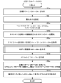
<内容>
1.比較例
1.1 露光システム
1.1.1 構成
1.1.2 動作
1.2 レーザ装置100
1.2.1 構成
1.2.2 動作
1.3 狭帯域化モジュール14
1.3.1 構成
1.3.2 動作
1.4 スキャン露光
1.5 周期的な波長変化及び積算スペクトル
1.6 光近接効果補正(OPC)
1.6.1 概要
1.6.2 モデルベースOPC
1.6.3 ルールベースOPC
1.7 比較例の課題
2.分割モデルベースOPC
2.1 動作
2.2 作用
3.共通モデルベースOPC
3.1 動作
3.2 作用
4.分割ルールベースOPC
4.1 動作
4.2 作用
5.その他 <Contents>
1. Comparative Example 1.1 Exposure System 1.1.1 Configuration 1.1.2 Operation 1.2 Laser Apparatus 100
1.2.1 Configuration 1.2.2 Operation 1.3Band narrowing module 14
1.3.1 Configuration 1.3.2 Operation 1.4 Scan Exposure 1.5 Periodic Wavelength Change and Integrated Spectrum 1.6 Optical Proximity Correction (OPC)
1.6.1 Overview 1.6.2 Model-based OPC
1.6.3 Rule-based OPC
1.7 Problem of Comparative Example 2. Split model-based OPC
2.1 Operation 2.2 Action3. Common model base OPC
3.1 Operation 3.2 Function 4. Division rule-based OPC
4.1 Operation 4.2 Function 5. others
1.比較例
1.1 露光システム
1.1.1 構成
1.1.2 動作
1.2 レーザ装置100
1.2.1 構成
1.2.2 動作
1.3 狭帯域化モジュール14
1.3.1 構成
1.3.2 動作
1.4 スキャン露光
1.5 周期的な波長変化及び積算スペクトル
1.6 光近接効果補正(OPC)
1.6.1 概要
1.6.2 モデルベースOPC
1.6.3 ルールベースOPC
1.7 比較例の課題
2.分割モデルベースOPC
2.1 動作
2.2 作用
3.共通モデルベースOPC
3.1 動作
3.2 作用
4.分割ルールベースOPC
4.1 動作
4.2 作用
5.その他 <Contents>
1. Comparative Example 1.1 Exposure System 1.1.1 Configuration 1.1.2 Operation 1.2 Laser Apparatus 100
1.2.1 Configuration 1.2.2 Operation 1.3
1.3.1 Configuration 1.3.2 Operation 1.4 Scan Exposure 1.5 Periodic Wavelength Change and Integrated Spectrum 1.6 Optical Proximity Correction (OPC)
1.6.1 Overview 1.6.2 Model-based OPC
1.6.3 Rule-based OPC
1.7 Problem of Comparative Example 2. Split model-based OPC
2.1 Operation 2.2 Action3. Common model base OPC
3.1 Operation 3.2 Function 4. Division rule-based OPC
4.1 Operation 4.2 Function 5. others
以下、本開示の実施形態について、図面を参照しながら詳しく説明する。以下に説明される実施形態は、本開示のいくつかの例を示すものであって、本開示の内容を限定するものではない。また、各実施形態で説明される構成及び動作の全てが本開示の構成及び動作として必須であるとは限らない。なお、同一の構成要素には同一の参照符号を付して、重複する説明を省略する。
Hereinafter, embodiments of the present disclosure will be described in detail with reference to the drawings. The embodiments described below show some examples of the present disclosure and do not limit the content of the present disclosure. Also, not all the configurations and operations described in each embodiment are essential as the configurations and operations of the present disclosure. In addition, the same reference numerals are given to the same components, and redundant explanations are omitted.
1.比較例
1.1 露光システム
図1は、比較例における露光システムの構成を概略的に示す。本開示の比較例とは、出願人のみによって知られていると出願人が認識している形態であって、出願人が自認している公知例ではない。
露光システムは、レーザ装置100と、露光装置200と、を含む。図1においてはレーザ装置100が簡略化して示されている。 1. Comparative Example 1.1 Exposure System FIG. 1 schematically shows the configuration of an exposure system in a comparative example. The comparative examples of the present disclosure are forms known by the applicant to be known only by the applicant, and not known examples to which the applicant admits.
The exposure system includes a laser device 100 and anexposure device 200 . A laser device 100 is shown in simplified form in FIG.
1.1 露光システム
図1は、比較例における露光システムの構成を概略的に示す。本開示の比較例とは、出願人のみによって知られていると出願人が認識している形態であって、出願人が自認している公知例ではない。
露光システムは、レーザ装置100と、露光装置200と、を含む。図1においてはレーザ装置100が簡略化して示されている。 1. Comparative Example 1.1 Exposure System FIG. 1 schematically shows the configuration of an exposure system in a comparative example. The comparative examples of the present disclosure are forms known by the applicant to be known only by the applicant, and not known examples to which the applicant admits.
The exposure system includes a laser device 100 and an
レーザ装置100は、レーザ制御プロセッサ130を含む。レーザ制御プロセッサ130は、制御プログラムが記憶されたメモリ132と、制御プログラムを実行するCPU(central processing unit)131と、を含む処理装置である。レーザ制御プロセッサ130は本開示に含まれる各種処理を実行するために特別に構成又はプログラムされている。レーザ装置100は、パルスレーザ光を露光装置200に向けて出力するように構成されている。
The laser device 100 includes a laser control processor 130 . The laser control processor 130 is a processing device that includes a memory 132 storing a control program and a CPU (central processing unit) 131 that executes the control program. Laser control processor 130 is specially configured or programmed to perform the various processes contained in this disclosure. The laser device 100 is configured to output pulsed laser light toward the exposure device 200 .
1.1.1 構成
図1に示されるように、露光装置200は、照明光学系201と、投影光学系202と、露光制御プロセッサ210と、を含む。
照明光学系201は、レーザ装置100から入射したパルスレーザ光によって、マスクステージMS上に配置された図示しないフォトマスクのマスクパターンを照明する。 1.1.1 Configuration As shown in FIG. 1, theexposure apparatus 200 includes an illumination optical system 201, a projection optical system 202, and an exposure control processor 210. As shown in FIG.
The illuminationoptical system 201 illuminates a mask pattern of a photomask (not shown) placed on the mask stage MS with pulsed laser light incident from the laser device 100 .
図1に示されるように、露光装置200は、照明光学系201と、投影光学系202と、露光制御プロセッサ210と、を含む。
照明光学系201は、レーザ装置100から入射したパルスレーザ光によって、マスクステージMS上に配置された図示しないフォトマスクのマスクパターンを照明する。 1.1.1 Configuration As shown in FIG. 1, the
The illumination
投影光学系202は、フォトマスクを透過したパルスレーザ光を縮小投影して、ワークピーステーブルWT上に配置された図示しないワークピースに結像させる。ワークピースはレジスト膜が塗布された半導体ウエハ等の感光基板である。
The projection optical system 202 reduces and projects the pulsed laser beam that has passed through the photomask, and forms an image on a workpiece (not shown) placed on the workpiece table WT. The workpiece is a photosensitive substrate such as a semiconductor wafer coated with a resist film.
露光制御プロセッサ210は、制御プログラムが記憶されたメモリ212と、制御プログラムを実行するCPU211と、を含む処理装置である。露光制御プロセッサ210は本開示に含まれる各種処理を実行するために特別に構成又はプログラムされている。露光制御プロセッサ210は、露光装置200の制御を統括するとともに、レーザ制御プロセッサ130との間で各種パラメータ及び各種信号を送受信する。
The exposure control processor 210 is a processing device that includes a memory 212 storing control programs and a CPU 211 that executes the control programs. Exposure control processor 210 is specially configured or programmed to perform the various processes contained in this disclosure. The exposure control processor 210 supervises the control of the exposure apparatus 200 and transmits/receives various parameters and various signals to/from the laser control processor 130 .
1.1.2 動作
露光制御プロセッサ210は、目標長波長λL及び目標短波長λSと電圧指令値とを含む各種パラメータと、トリガ信号と、をレーザ制御プロセッサ130に送信する。レーザ制御プロセッサ130は、これらのパラメータ及び信号に従ってレーザ装置100を制御する。 1.1.2 Operation Theexposure control processor 210 transmits various parameters including the target long wavelength λL, target short wavelength λS, and voltage command value, and a trigger signal to the laser control processor 130 . Laser control processor 130 controls laser device 100 according to these parameters and signals.
露光制御プロセッサ210は、目標長波長λL及び目標短波長λSと電圧指令値とを含む各種パラメータと、トリガ信号と、をレーザ制御プロセッサ130に送信する。レーザ制御プロセッサ130は、これらのパラメータ及び信号に従ってレーザ装置100を制御する。 1.1.2 Operation The
露光制御プロセッサ210は、マスクステージMSとワークピーステーブルWTとを同期して互いに逆方向に平行移動させる。これにより、マスクパターンを反映したパルスレーザ光でワークピースが露光される。
このようなフォトリソグラフィによって感光基板にマスクパターンが転写される。その後、複数の工程を経ることで電子デバイスを製造することができる。Exposure control processor 210 synchronously translates mask stage MS and workpiece table WT in opposite directions. As a result, the workpiece is exposed to pulsed laser light that reflects the mask pattern.
A mask pattern is transferred to a photosensitive substrate by such photolithography. After that, an electronic device can be manufactured through a plurality of steps.
このようなフォトリソグラフィによって感光基板にマスクパターンが転写される。その後、複数の工程を経ることで電子デバイスを製造することができる。
A mask pattern is transferred to a photosensitive substrate by such photolithography. After that, an electronic device can be manufactured through a plurality of steps.
1.2 レーザ装置100
1.2.1 構成
図2は、レーザ装置100の構成を概略的に示す。図2に、互いに垂直なV軸、H軸、及びZ軸が示されている。図2においては、-V方向に見たレーザ装置100が示され、露光装置200は簡略化して示されている。 1.2 Laser Device 100
1.2.1 Configuration FIG. 2 schematically shows the configuration of the laser device 100. As shown in FIG. FIG. 2 shows V-, H-, and Z-axes that are perpendicular to each other. FIG. 2 shows the laser device 100 viewed in the -V direction, and theexposure device 200 is simplified.
1.2.1 構成
図2は、レーザ装置100の構成を概略的に示す。図2に、互いに垂直なV軸、H軸、及びZ軸が示されている。図2においては、-V方向に見たレーザ装置100が示され、露光装置200は簡略化して示されている。 1.2 Laser Device 100
1.2.1 Configuration FIG. 2 schematically shows the configuration of the laser device 100. As shown in FIG. FIG. 2 shows V-, H-, and Z-axes that are perpendicular to each other. FIG. 2 shows the laser device 100 viewed in the -V direction, and the
レーザ装置100は、レーザ制御プロセッサ130の他に、レーザチャンバ10と、パルスパワーモジュール(PPM)13と、狭帯域化モジュール14と、出力結合ミラー15と、モニタモジュール17と、を含む。狭帯域化モジュール14及び出力結合ミラー15は光共振器を構成する。
The laser device 100 includes a laser chamber 10 , a pulse power module (PPM) 13 , a band narrowing module 14 , an output coupling mirror 15 and a monitor module 17 in addition to the laser control processor 130 . The band narrowing module 14 and the output coupling mirror 15 constitute an optical resonator.
レーザチャンバ10は、光共振器の光路に配置されている。レーザチャンバ10にはウインドウ10a及び10bが設けられている。
レーザチャンバ10は、放電電極11a及びこれと対をなす図示しない放電電極を内部に備えている。図示しない放電電極は、V軸の方向において放電電極11aと重なるように位置している。レーザチャンバ10には、例えばレアガスとしてアルゴンガス又はクリプトンガス、ハロゲンガスとしてフッ素ガス、バッファガスとしてネオンガス等を含むレーザガスが封入される。 Alaser chamber 10 is arranged in the optical path of the optical resonator. A laser chamber 10 is provided with windows 10a and 10b.
Thelaser chamber 10 internally includes a discharge electrode 11a and a discharge electrode (not shown) paired with the discharge electrode 11a. A discharge electrode (not shown) is positioned so as to overlap the discharge electrode 11a in the V-axis direction. The laser chamber 10 is filled with a laser gas containing, for example, argon gas or krypton gas as a rare gas, fluorine gas as a halogen gas, and neon gas as a buffer gas.
レーザチャンバ10は、放電電極11a及びこれと対をなす図示しない放電電極を内部に備えている。図示しない放電電極は、V軸の方向において放電電極11aと重なるように位置している。レーザチャンバ10には、例えばレアガスとしてアルゴンガス又はクリプトンガス、ハロゲンガスとしてフッ素ガス、バッファガスとしてネオンガス等を含むレーザガスが封入される。 A
The
パルスパワーモジュール13は、図示しないスイッチを含むとともに、図示しない充電器に接続されている。
The pulse power module 13 includes a switch (not shown) and is connected to a charger (not shown).
狭帯域化モジュール14は、プリズム41~43と、グレーティング53と、ミラー63と、を含む。狭帯域化モジュール14の詳細については後述する。
出力結合ミラー15は、部分反射ミラーで構成されている。 Band narrowingmodule 14 includes prisms 41 - 43 , grating 53 and mirror 63 . Details of the band narrowing module 14 will be described later.
Theoutput coupling mirror 15 consists of a partially reflective mirror.
出力結合ミラー15は、部分反射ミラーで構成されている。 Band narrowing
The
出力結合ミラー15から出力されたパルスレーザ光の光路に、パルスレーザ光の一部を高い透過率で透過させ、他の一部を反射するビームスプリッタ16が配置されている。ビームスプリッタ16によって反射されたパルスレーザ光の光路に、モニタモジュール17が配置されている。
A beam splitter 16 is arranged in the optical path of the pulsed laser light output from the output coupling mirror 15 to transmit part of the pulsed laser light with high transmittance and reflect the other part. A monitor module 17 is arranged in the optical path of the pulsed laser beam reflected by the beam splitter 16 .
1.2.2 動作
レーザ制御プロセッサ130は、露光制御プロセッサ210から目標長波長λL及び目標短波長λSと、電圧指令値と、を含む各種パラメータを取得する。レーザ制御プロセッサ130は、目標長波長λL及び目標短波長λSに基づいて狭帯域化モジュール14に制御信号を送信する。 1.2.2 Operation Thelaser control processor 130 acquires various parameters including the target long wavelength λL, the target short wavelength λS, and the voltage command value from the exposure control processor 210 . Laser control processor 130 sends a control signal to narrowband module 14 based on target long wavelength λL and target short wavelength λS.
レーザ制御プロセッサ130は、露光制御プロセッサ210から目標長波長λL及び目標短波長λSと、電圧指令値と、を含む各種パラメータを取得する。レーザ制御プロセッサ130は、目標長波長λL及び目標短波長λSに基づいて狭帯域化モジュール14に制御信号を送信する。 1.2.2 Operation The
レーザ制御プロセッサ130は、露光制御プロセッサ210からトリガ信号を受信する。レーザ制御プロセッサ130は、トリガ信号に基づく発振トリガ信号をパルスパワーモジュール13に送信する。パルスパワーモジュール13に含まれるスイッチは、レーザ制御プロセッサ130から発振トリガ信号を受信するとオン状態となる。パルスパワーモジュール13は、スイッチがオン状態となると、充電器に充電された電気エネルギーからパルス状の高電圧を生成し、この高電圧を放電電極11aに印加する。
The laser control processor 130 receives trigger signals from the exposure control processor 210 . The laser control processor 130 transmits an oscillation trigger signal based on the trigger signal to the pulse power module 13 . A switch included in the pulse power module 13 is turned on when an oscillation trigger signal is received from the laser control processor 130 . When the switch is turned on, the pulse power module 13 generates a pulsed high voltage from the electrical energy charged in the charger, and applies this high voltage to the discharge electrode 11a.
放電電極11aに高電圧が印加されると、放電電極11a及び図示しない放電電極の間の放電空間に放電が起こる。この放電のエネルギーにより、レーザチャンバ10内のレーザガスが励起されて高エネルギー準位に移行する。励起されたレーザガスが、その後、低エネルギー準位に移行するとき、そのエネルギー準位差に応じた波長の光を放出する。
When a high voltage is applied to the discharge electrode 11a, discharge occurs in the discharge space between the discharge electrode 11a and a discharge electrode (not shown). The energy of this discharge excites the laser gas in the laser chamber 10 to shift to a high energy level. When the excited laser gas then shifts to a lower energy level, it emits light with a wavelength corresponding to the energy level difference.
レーザチャンバ10内で発生した光は、ウインドウ10a及び10bを介してレーザチャンバ10の外部に出射する。ウインドウ10aから出射した光は、狭帯域化モジュール14に入射する。狭帯域化モジュール14に入射した光のうちの所望波長付近の光が、狭帯域化モジュール14によって折り返されてレーザチャンバ10に戻される。
The light generated within the laser chamber 10 is emitted outside the laser chamber 10 through the windows 10a and 10b. Light emitted from the window 10 a enters the band narrowing module 14 . Of the light incident on the band-narrowing module 14 , light near the desired wavelength is folded back by the band-narrowing module 14 and returned to the laser chamber 10 .
出力結合ミラー15は、ウインドウ10bから出射した光のうちの一部を透過させて出力し、他の一部を反射してレーザチャンバ10に戻す。
The output coupling mirror 15 transmits and outputs part of the light emitted from the window 10 b and reflects the other part back to the laser chamber 10 .
このようにして、レーザチャンバ10から出射した光は、狭帯域化モジュール14と出力結合ミラー15との間で往復する。この光は、レーザチャンバ10内の放電空間を通過する度に増幅される。また、この光は、狭帯域化モジュール14によって折り返される度に狭帯域化され、狭帯域化モジュール14による選択波長の範囲の一部を中心波長とした急峻な波長分布を有する光となる。こうしてレーザ発振し狭帯域化された光が、出力結合ミラー15からパルスレーザ光として出力される。
In this way, light emitted from the laser chamber 10 reciprocates between the band narrowing module 14 and the output coupling mirror 15 . This light is amplified each time it passes through the discharge space within the laser chamber 10 . Further, this light is band-narrowed each time it is folded back by the band-narrowing module 14, and becomes light having a steep wavelength distribution with a part of the range of wavelengths selected by the band-narrowing module 14 as the central wavelength. The laser-oscillated and narrow-band light is output from the output coupling mirror 15 as a pulsed laser light.
モニタモジュール17は、パルスレーザ光の中心波長を計測し、計測波長をレーザ制御プロセッサ130に送信する。レーザ制御プロセッサ130は、計測波長に基づいて狭帯域化モジュール14をフィードバック制御する。
ビームスプリッタ16を透過したパルスレーザ光は、露光装置200へ入射する。 Themonitor module 17 measures the central wavelength of the pulsed laser beam and transmits the measured wavelength to the laser control processor 130 . A laser control processor 130 feedback controls the band narrowing module 14 based on the measured wavelength.
The pulsed laser light that has passed through thebeam splitter 16 enters the exposure device 200 .
ビームスプリッタ16を透過したパルスレーザ光は、露光装置200へ入射する。 The
The pulsed laser light that has passed through the
1.3 狭帯域化モジュール14
1.3.1 構成
プリズム41~43は、ウインドウ10aから出射した光ビームの光路にこれらの番号の小さい方から順に配置されている。プリズム41~43は、光ビームが入出射するプリズム41~43の表面がいずれもV軸に平行となるように配置されている。プリズム43は、回転ステージ143によってV軸に平行な軸周りに回転可能となっている。 1.3Band narrowing module 14
1.3.1 Configuration Theprisms 41 to 43 are arranged on the optical path of the light beam emitted from the window 10a in ascending order of their numbers. The prisms 41 to 43 are arranged so that the surfaces of the prisms 41 to 43 through which light beams enter and exit are all parallel to the V-axis. The prism 43 is rotatable around an axis parallel to the V-axis by a rotating stage 143 .
1.3.1 構成
プリズム41~43は、ウインドウ10aから出射した光ビームの光路にこれらの番号の小さい方から順に配置されている。プリズム41~43は、光ビームが入出射するプリズム41~43の表面がいずれもV軸に平行となるように配置されている。プリズム43は、回転ステージ143によってV軸に平行な軸周りに回転可能となっている。 1.3
1.3.1 Configuration The
ミラー63は、プリズム41~43を透過した光ビームの光路に配置されている。ミラー63は、光ビームを反射する表面がV軸に平行となるように配置されており、回転ステージ163によってV軸に平行な軸周りに回転可能となっている。
The mirror 63 is arranged in the optical path of the light beams transmitted through the prisms 41-43. The mirror 63 is arranged so that the surface that reflects the light beam is parallel to the V-axis, and is rotatable around an axis parallel to the V-axis by a rotating stage 163 .
グレーティング53は、ミラー63によって反射された光ビームの光路に配置されている。グレーティング53の溝の方向は、V軸に平行である。
The grating 53 is arranged in the optical path of the light beam reflected by the mirror 63. The direction of the grooves of the grating 53 is parallel to the V-axis.
1.3.2 動作
ウインドウ10aから出射した光ビームは、プリズム41~43の各々によって、V軸に垂直な面であるHZ面に平行な面内で進行方向を変えられ、HZ面に平行な面内でビーム幅を拡大させられる。
プリズム41~43を透過した光ビームは、ミラー63によって反射されてグレーティング53に入射する。 1.3.2 Operation The light beam emitted from thewindow 10a is changed in direction by each of the prisms 41 to 43 in a plane parallel to the HZ plane, which is a plane perpendicular to the V axis, and becomes parallel to the HZ plane. The beam width can be expanded in the plane.
The light beams transmitted through theprisms 41 to 43 are reflected by the mirror 63 and enter the grating 53 .
ウインドウ10aから出射した光ビームは、プリズム41~43の各々によって、V軸に垂直な面であるHZ面に平行な面内で進行方向を変えられ、HZ面に平行な面内でビーム幅を拡大させられる。
プリズム41~43を透過した光ビームは、ミラー63によって反射されてグレーティング53に入射する。 1.3.2 Operation The light beam emitted from the
The light beams transmitted through the
グレーティング53に入射した光ビームは、グレーティング53の複数の溝によって反射されるとともに、光の波長に応じた方向に回折させられる。グレーティング53は、ミラー63からグレーティング53に入射する光ビームの入射角と、所望波長の回折光の回折角と、が一致するようにリトロー配置とされる。
A light beam incident on the grating 53 is reflected by the plurality of grooves of the grating 53 and diffracted in a direction according to the wavelength of the light. The grating 53 has a Littrow arrangement so that the incident angle of the light beam incident on the grating 53 from the mirror 63 and the diffraction angle of the diffracted light of the desired wavelength match.
ミラー63及びプリズム41~43は、グレーティング53から戻された光ビームのビーム幅をHZ面に平行な面内で縮小させるとともに、その光ビームを、ウインドウ10aを介してレーザチャンバ10の内部に戻す。
The mirror 63 and prisms 41-43 reduce the beam width of the light beam returned from the grating 53 in a plane parallel to the HZ plane, and return the light beam to the interior of the laser chamber 10 through the window 10a. .
レーザ制御プロセッサ130は、図示しないドライバを介して回転ステージ143及び163を制御する。回転ステージ143及び163の回転角度に応じて、グレーティング53に入射する光ビームの入射角が変化し、狭帯域化モジュール14によって選択される波長が変化する。回転ステージ143は主に粗調整に使用され、回転ステージ163は主に微調整に使用される。
The laser control processor 130 controls the rotation stages 143 and 163 via drivers (not shown). Depending on the rotation angles of the rotation stages 143 and 163, the incident angle of the light beam incident on the grating 53 changes, and the wavelength selected by the band narrowing module 14 changes. Rotating stage 143 is mainly used for coarse adjustment, and rotating stage 163 is mainly used for fine adjustment.
レーザ制御プロセッサ130は、露光制御プロセッサ210から受信した目標長波長λL及び目標短波長λSに基づいて、ミラー63の姿勢が複数のパルスごとに周期的に変化するように、回転ステージ163を制御する。これにより、パルスレーザ光の中心波長が複数のパルスごとに目標長波長λLと目標短波長λSとの間で周期的に変化する。このように、レーザ装置100は複数波長でレーザ発振を行うことができる。
Based on the target long wavelength λL and the target short wavelength λS received from the exposure control processor 210, the laser control processor 130 controls the rotation stage 163 so that the attitude of the mirror 63 periodically changes for each pulse. . As a result, the central wavelength of the pulsed laser light periodically changes between the target long wavelength λL and the target short wavelength λS for every plurality of pulses. Thus, the laser device 100 can perform laser oscillation at multiple wavelengths.
露光装置200における焦点距離は、パルスレーザ光の波長に依存する。複数波長でレーザ発振して露光装置200に入射したパルスレーザ光は、パルスレーザ光の光路軸の方向において複数の異なる位置で結像することができるので、実質的に焦点深度を大きくすることができる。例えば、膜厚の大きいレジスト膜を露光する場合でも、レジスト膜の厚み方向での結像性能を維持し得る。あるいは、現像されたレジスト膜の断面形状を示すレジストプロファイルを調整し得る。
The focal length of the exposure apparatus 200 depends on the wavelength of the pulsed laser light. The pulsed laser light that is oscillated at a plurality of wavelengths and is incident on the exposure apparatus 200 can form images at a plurality of different positions in the direction of the optical path axis of the pulsed laser light, so that the depth of focus can be substantially increased. can. For example, even when a resist film having a large thickness is exposed, the imaging performance in the thickness direction of the resist film can be maintained. Alternatively, a resist profile representing the cross-sectional shape of the developed resist film can be adjusted.
1.4 スキャン露光
図3~図5は、パルスレーザ光の位置に対して感光基板のスキャンフィールドSFの位置が変化する様子を示す。感光基板は、例えば、ほぼ円板形を有する単結晶シリコンの板であり、例えば感光性のレジスト膜が塗布されている。スキャンフィールドSFは、例えば、感光基板に形成される多数の半導体チップのうちのいくつかの半導体チップが形成される領域であって、1枚のマスクのマスクパターンが1回のスキャンで転写される領域に相当する。1つのスキャンフィールドSFを露光するときはパルスレーザ光が所定の繰り返し周波数で連続して出力される。パルスレーザ光を所定の繰り返し周波数で連続して出力することをバースト出力という。1つのスキャンフィールドSFから他のスキャンフィールドSFに露光位置を移動させるときはパルスレーザ光の出力を休止する。従って、1つの感光基板を露光するために、バースト出力が複数回にわたって繰り返される。 1.4 Scan Exposure FIGS. 3 to 5 show how the position of the scan field SF of the photosensitive substrate changes with respect to the position of the pulsed laser beam. The photosensitive substrate is, for example, a plate of monocrystalline silicon having a substantially disk shape and is coated with, for example, a photosensitive resist film. The scan field SF is, for example, a region where some semiconductor chips out of a large number of semiconductor chips formed on the photosensitive substrate are formed, and the mask pattern of one mask is transferred by one scan. Corresponds to area. When exposing one scan field SF, pulsed laser light is continuously output at a predetermined repetition frequency. Continuous output of pulsed laser light at a predetermined repetition frequency is called burst output. When moving the exposure position from one scan field SF to another scan field SF, the output of the pulsed laser light is stopped. Therefore, the burst output is repeated multiple times to expose one photosensitive substrate.
図3~図5は、パルスレーザ光の位置に対して感光基板のスキャンフィールドSFの位置が変化する様子を示す。感光基板は、例えば、ほぼ円板形を有する単結晶シリコンの板であり、例えば感光性のレジスト膜が塗布されている。スキャンフィールドSFは、例えば、感光基板に形成される多数の半導体チップのうちのいくつかの半導体チップが形成される領域であって、1枚のマスクのマスクパターンが1回のスキャンで転写される領域に相当する。1つのスキャンフィールドSFを露光するときはパルスレーザ光が所定の繰り返し周波数で連続して出力される。パルスレーザ光を所定の繰り返し周波数で連続して出力することをバースト出力という。1つのスキャンフィールドSFから他のスキャンフィールドSFに露光位置を移動させるときはパルスレーザ光の出力を休止する。従って、1つの感光基板を露光するために、バースト出力が複数回にわたって繰り返される。 1.4 Scan Exposure FIGS. 3 to 5 show how the position of the scan field SF of the photosensitive substrate changes with respect to the position of the pulsed laser beam. The photosensitive substrate is, for example, a plate of monocrystalline silicon having a substantially disk shape and is coated with, for example, a photosensitive resist film. The scan field SF is, for example, a region where some semiconductor chips out of a large number of semiconductor chips formed on the photosensitive substrate are formed, and the mask pattern of one mask is transferred by one scan. Corresponds to area. When exposing one scan field SF, pulsed laser light is continuously output at a predetermined repetition frequency. Continuous output of pulsed laser light at a predetermined repetition frequency is called burst output. When moving the exposure position from one scan field SF to another scan field SF, the output of the pulsed laser light is stopped. Therefore, the burst output is repeated multiple times to expose one photosensitive substrate.
スキャンフィールドSFのX軸方向の幅は、ワークピーステーブルWT(図1参照)の位置におけるパルスレーザ光のビーム断面BのX軸方向の幅に相当する。スキャンフィールドSFのY軸方向の幅は、ワークピーステーブルWTの位置におけるパルスレーザ光のビーム断面BのY軸方向の幅Wより大きい。
The width of the scan field SF in the X-axis direction corresponds to the width in the X-axis direction of the beam cross section B of the pulsed laser light at the position of the workpiece table WT (see FIG. 1). The width of the scan field SF in the Y-axis direction is larger than the width W in the Y-axis direction of the beam cross section B of the pulsed laser light at the position of the workpiece table WT.
パルスレーザ光によりスキャンフィールドSFをスキャンして露光する手順は、図3、図4、図5の順で行われる。まず、図3に示されるように、ビーム断面Bの-Y方向の端By-の位置に対してスキャンフィールドSFの+Y方向の端SFy+が-Y方向に所定距離離れて位置するようにワークピーステーブルWTが位置決めされる。そして、ビーム断面Bの-Y方向の端By-の位置に対してスキャンフィールドSFの+Y方向の端SFy+が一致するまでに速度Vyとなるように、ワークピーステーブルWTが+Y方向に加速される。図4に示されるように、ビーム断面Bの位置に対してスキャンフィールドSFの位置が速度Vyで等速直線運動するようにワークピーステーブルWTを+Y方向に移動しながら、スキャンフィールドSFが露光される。図5に示されるように、ビーム断面Bの+Y方向の端By+の位置をスキャンフィールドSFの-Y方向の端SFy-が通過するまでワークピーステーブルWTが移動されたら、スキャンフィールドSFのスキャンが終了する。
The procedure for scanning and exposing the scan field SF with the pulsed laser light is performed in the order of FIGS. First, as shown in FIG. 3, the workpiece is positioned so that the +Y direction end SFy+ of the scan field SF is located at a predetermined distance in the −Y direction from the position of the −Y direction end By− of the beam cross section B. A table WT is positioned. Then, the work piece table WT is accelerated in the +Y direction so that the +Y direction end SFy+ of the scan field SF coincides with the position of the −Y direction end By− of the beam cross section B so as to reach a velocity Vy. . As shown in FIG. 4, the scan field SF is exposed while moving the work piece table WT in the +Y direction so that the position of the scan field SF performs uniform linear motion at a velocity Vy with respect to the position of the beam cross section B. be. As shown in FIG. 5, when the workpiece table WT is moved until the -Y-direction end SFy- of the scan field SF passes the position of the +Y-direction end By+ of the beam cross-section B, scanning of the scan field SF is started. finish.
このように、ビーム断面Bの位置に対してスキャンフィールドSFが移動しながら露光が行われる。スキャンフィールドSFを基準にすると、パルスレーザ光によって-Y方向にスキャンするということもできる。-Y方向は本開示における第1の方向に相当する。
In this manner, exposure is performed while the scan field SF moves with respect to the position of the beam cross section B. Using the scan field SF as a reference, it can be said that scanning is performed in the -Y direction by the pulsed laser beam. The -Y direction corresponds to the first direction in this disclosure.
パルスレーザ光のビーム断面Bの幅Wに相当する距離をスキャンフィールドSFが速度Vyで移動するための所要時間Tsは、以下の通りである。
Ts=W/Vy
スキャンフィールドSFのうちの任意の1箇所に照射されるパルスレーザ光の照射パルス数Nsは、所要時間Tsにおいて生成されるパルスレーザ光のパルス数と同一であり、以下の通りである。
Ns=F・Ts
ここで、Fはパルスレーザ光の繰返し周波数である。
照射パルス数Nsは、Nスリットパルス数ともいう。 The required time Ts for the scan field SF to move at the speed Vy over a distance corresponding to the width W of the beam cross section B of the pulsed laser light is as follows.
Ts=W/Vy
The irradiation pulse number Ns of the pulsed laser light irradiated to an arbitrary point in the scan field SF is the same as the pulse number of the pulsed laser light generated in the required time Ts, and is as follows.
Ns=F・Ts
Here, F is the repetition frequency of the pulsed laser light.
The irradiation pulse number Ns is also referred to as the N slit pulse number.
Ts=W/Vy
スキャンフィールドSFのうちの任意の1箇所に照射されるパルスレーザ光の照射パルス数Nsは、所要時間Tsにおいて生成されるパルスレーザ光のパルス数と同一であり、以下の通りである。
Ns=F・Ts
ここで、Fはパルスレーザ光の繰返し周波数である。
照射パルス数Nsは、Nスリットパルス数ともいう。 The required time Ts for the scan field SF to move at the speed Vy over a distance corresponding to the width W of the beam cross section B of the pulsed laser light is as follows.
Ts=W/Vy
The irradiation pulse number Ns of the pulsed laser light irradiated to an arbitrary point in the scan field SF is the same as the pulse number of the pulsed laser light generated in the required time Ts, and is as follows.
Ns=F・Ts
Here, F is the repetition frequency of the pulsed laser light.
The irradiation pulse number Ns is also referred to as the N slit pulse number.
ここでは電子デバイスを製造するための感光基板に含まれるスキャンフィールドSFについて説明したが、後述のテストウエハに含まれるスキャンフィールドSFについても同様である。
Although the scan field SF included in the photosensitive substrate for manufacturing the electronic device has been described here, the same applies to the scan field SF included in the test wafer described later.
1.5 周期的な波長変化及び積算スペクトル
図6は、周期的な波長変化を示すグラフである。図6において、横軸は時間tを示し、縦軸は波長λを示す。図6に示される小円の各々は、パルスレーザ光が出力されるときの時間tと、そのときの中心波長と、を示す。 1.5 Periodic Wavelength Change and Integrated Spectrum FIG. 6 is a graph showing periodic wavelength change. In FIG. 6, the horizontal axis indicates time t, and the vertical axis indicates wavelength λ. Each small circle shown in FIG. 6 indicates the time t when the pulsed laser light is output and the center wavelength at that time.
図6は、周期的な波長変化を示すグラフである。図6において、横軸は時間tを示し、縦軸は波長λを示す。図6に示される小円の各々は、パルスレーザ光が出力されるときの時間tと、そのときの中心波長と、を示す。 1.5 Periodic Wavelength Change and Integrated Spectrum FIG. 6 is a graph showing periodic wavelength change. In FIG. 6, the horizontal axis indicates time t, and the vertical axis indicates wavelength λ. Each small circle shown in FIG. 6 indicates the time t when the pulsed laser light is output and the center wavelength at that time.
図6に示される例では、目標長波長λLと目標短波長λSとの間で、中心波長が周期的に変化する。波長変化の1周期分のパルス数をNとする。波長変化の周期Tは以下の式で与えられる。
T=N/F In the example shown in FIG. 6, the center wavelength changes periodically between the target long wavelength λL and the target short wavelength λS. Let N be the number of pulses for one period of wavelength change. The wavelength change period T is given by the following equation.
T=N/F
T=N/F In the example shown in FIG. 6, the center wavelength changes periodically between the target long wavelength λL and the target short wavelength λS. Let N be the number of pulses for one period of wavelength change. The wavelength change period T is given by the following equation.
T=N/F
図7は、複数の中心波長が含まれるパルスレーザ光の積算スペクトルを示す。図7に示される積算スペクトルは、図6に示される波長変化の1周期分の積算スペクトルに相当する。図7において、横軸は波長λを示し、縦軸は光強度Iを示す。破線は1パルスごとのパルスレーザ光のスペクトルを示し、それぞれの中心波長はピーク波長に一致していてもよい。図6に示されるように目標長波長λLと目標短波長λSとの間で多段階に中心波長を変化させることにより、図7に示される積算スペクトルは目標長波長λLと目標短波長λSとの間でほぼ均一な光強度Iを有するフラットトップ状となり得る。
FIG. 7 shows an integrated spectrum of pulsed laser light containing a plurality of central wavelengths. The integrated spectrum shown in FIG. 7 corresponds to the integrated spectrum for one cycle of wavelength change shown in FIG. In FIG. 7, the horizontal axis indicates the wavelength λ, and the vertical axis indicates the light intensity I. A dashed line indicates the spectrum of the pulsed laser light for each pulse, and the center wavelength of each line may match the peak wavelength. By changing the central wavelength in multiple stages between the target long wavelength λL and the target short wavelength λS as shown in FIG. 6, the integrated spectrum shown in FIG. It can be flat-topped with a light intensity I that is nearly uniform between them.
スキャンフィールドSFのうちの任意の1箇所に照射されるパルスレーザ光の照射パルス数Nsは、波長変化の1周期分のパルス数Nの倍数であることが望ましい。これにより、スキャンフィールドSFのどの部分においても、同じ積算スペクトルを有する照射パルス数Nsのパルスレーザ光が照射されることになる。これにより、照射位置による露光結果のばらつきが少なく、高品質の電子デバイスを製造することができる。
It is desirable that the irradiation pulse number Ns of the pulsed laser light irradiated to an arbitrary point in the scan field SF is a multiple of the pulse number N for one period of wavelength change. As a result, any portion of the scan field SF is irradiated with the pulsed laser light having the same integrated spectrum and the irradiation pulse number Ns. As a result, it is possible to manufacture high-quality electronic devices with little variation in exposure results depending on the irradiation position.
1.6 光近接効果補正(OPC)
1.6.1 概要
フォトリソグラフィにおいて、設計された目標パターンGの寸法が露光光源の波長より小さくなると、目標パターンGをそのままマスクに描画して露光しても、目標パターンGと同等のウエハパターンを得られないことがある。そこで、目標パターンGと同等のウエハパターンを得られるように、予め目標パターンGを補正して補正マスクパターンFを作成することを、光近接効果補正(optical proximity correction;OPC)と呼ぶ。 1.6 Optical Proximity Correction (OPC)
1.6.1 Overview In photolithography, when the dimension of the designed target pattern G becomes smaller than the wavelength of the exposure light source, even if the target pattern G is drawn on a mask as it is and exposed, a wafer pattern equivalent to the target pattern G is obtained. may not be obtained. Accordingly, creating a corrected mask pattern F by correcting the target pattern G in advance so that a wafer pattern equivalent to the target pattern G can be obtained is called optical proximity correction (OPC).
図8は、目標パターンGをそのままマスクパターンとして用いた場合に、光近接効果によって目標パターンGと異なるウエハパターンR1が形成された例を示す。例えば、目標パターンGに含まれる角部が、ウエハパターンR1において丸まったり、目標パターンGに含まれる凸状部が、ウエハパターンR1において後退したりといった影響がみられる。
FIG. 8 shows an example in which a wafer pattern R1 different from the target pattern G is formed due to the optical proximity effect when the target pattern G is used as the mask pattern as it is. For example, the corners included in the target pattern G may be rounded in the wafer pattern R1, and the convex portions included in the target pattern G may recede in the wafer pattern R1.
図9は、光近接効果補正が行われた補正マスクパターンFを用いた場合に、目標パターンGに近いウエハパターンR2が形成された例を示す。補正マスクパターンFは、例えば、目標パターンGにおける凸状の角部に張り出し部を追加したり、目標パターンGにおける凹み状の角部をさらに凹ませたり、補助パターンSRAF(sub-resolution assist feature)を追加したりといった変形を含む。これにより、目標パターンGに近い形状のウエハパターンR2を得ることができる。
FIG. 9 shows an example in which a wafer pattern R2 close to the target pattern G is formed when a corrected mask pattern F subjected to optical proximity correction is used. The correction mask pattern F may be, for example, adding an overhang to a convex corner of the target pattern G, further recessing a recessed corner of the target pattern G, or forming an auxiliary pattern SRAF (sub-resolution assist feature). Including modifications such as adding Thereby, a wafer pattern R2 having a shape close to the target pattern G can be obtained.
光近接効果補正においては、光近接効果の補正だけでなく、レジスト膜の現像やその他の半導体プロセスにおいて生じるマスクパターンとウエハパターンの違いを一緒に補正することもできる。
In the optical proximity correction, it is possible not only to correct the optical proximity effect, but also to correct the differences between the mask pattern and the wafer pattern that occur in resist film development and other semiconductor processes.
光近接効果補正としては、モデルベースOPC及びルールベースOPCの2種類が知られている。これらについて以下に説明する。
Two types of optical proximity correction are known: model-based OPC and rule-based OPC. These are described below.
1.6.2 モデルベースOPC
モデルベースOPCにおいては、目標パターンGに含まれる特徴的な形状ごとに行う露光シミュレーションの結果と、実際の露光結果と、に基づいてモデル関数群Mを作成する。このモデル関数群Mを用いて、目標パターンGと同等のウエハパターンを得るための補正マスクパターンFを作成する。モデルベースOPCは、主に130nmより小さい線幅世代で用いられている。 1.6.2 Model-based OPC
In model-based OPC, a model function group M is created based on the result of an exposure simulation performed for each characteristic shape included in the target pattern G and the actual exposure result. Using this model function group M, a correction mask pattern F for obtaining a wafer pattern equivalent to the target pattern G is created. Model-based OPC is mainly used in the sub-130 nm linewidth generation.
図10は、比較例におけるモデルベースOPCの概念図である。まず、目標パターンGに基づいてテストマスクパターンEを含むテストマスクを作成する。テストマスクを用いてテストウエハを露光し、パターニングされたテストウエハを計測して計測ウエハパターンDを取得する。
FIG. 10 is a conceptual diagram of model-based OPC in a comparative example. First, based on the target pattern G, a test mask including a test mask pattern E is created. A test wafer is exposed using a test mask, and the patterned test wafer is measured to obtain a measurement wafer pattern D. FIG.
テストマスクパターンEを用いた露光シミュレーションの結果と、実際の露光結果である計測ウエハパターンDと、に基づいて、露光シミュレーションの結果から実際の露光結果を予測するためのモデル関数群Mを作成する。このモデル関数群Mを用いて、目標パターンGから補正マスクパターンFを作成するためのプログラムであるOPCレシピPを作成する。目標パターンGを用いてOPCレシピPを実行することにより、補正マスクパターンFが作成される。補正マスクパターンFを用いて感光基板を露光することにより、目標パターンGに近いウエハパターンを得ることができる。
A model function group M for predicting the actual exposure result from the exposure simulation result is created based on the result of the exposure simulation using the test mask pattern E and the measurement wafer pattern D which is the actual exposure result. . Using this model function group M, an OPC recipe P, which is a program for creating a correction mask pattern F from a target pattern G, is created. By executing the OPC recipe P using the target pattern G, a correction mask pattern F is created. By exposing the photosensitive substrate using the correction mask pattern F, a wafer pattern close to the target pattern G can be obtained.
図11は、モデルベースOPCのフローチャートである。図11に示される処理は、主に、露光制御プロセッサ210などのプロセッサによって行われる。プロセッサは、図示しないマスク製造装置などの他の装置に含まれるものでもよく、そのようなプロセッサの構成は露光制御プロセッサ210と同様でよい。
FIG. 11 is a flowchart of model-based OPC. The processing shown in FIG. 11 is primarily performed by a processor such as the exposure control processor 210 . The processor may be included in another apparatus such as a mask manufacturing apparatus (not shown), and such a processor may have the same configuration as the exposure control processor 210 .
S1において、プロセッサは、目標パターンGを取得する。目標パターンGは、半導体チップの設計者が設計した感光基板の目標とするウエハパターンであり、例えばGDS(Graphic Data System)と呼ばれるデータフォーマットで提供される。目標パターンGは、感光基板のエッチングを行う場合はエッチング後のパターンでもよく、エッチングを行わない場合は露光後に現像されたレジスト膜のパターンでもよい。
At S1, the processor acquires the target pattern G. The target pattern G is a target wafer pattern of a photosensitive substrate designed by a semiconductor chip designer, and is provided in a data format called GDS (Graphic Data System), for example. The target pattern G may be a pattern after etching when the photosensitive substrate is etched, or may be a pattern of a resist film developed after exposure when etching is not performed.
S2において、プロセッサは、目標パターンGに基づいて露光条件を設定する。露光条件は、露光装置200の設定条件、例えば、照明光学系201(図1参照)による照明光源の形状、偏光照明の有無、及び投影光学系202の開口数を含む。また例えば、露光条件は、レジスト膜の種類、反射防止膜の有無及び種類、レジストスタック情報、レジスト膜の膜厚、レジスト膜の塗布条件、及び現像条件を含む。
In S2, the processor sets exposure conditions based on the target pattern G. The exposure conditions include setting conditions of the exposure apparatus 200 , such as the shape of the illumination light source of the illumination optical system 201 (see FIG. 1), the presence or absence of polarized illumination, and the numerical aperture of the projection optical system 202 . Further, for example, the exposure conditions include the type of resist film, the presence or absence and type of antireflection film, resist stack information, film thickness of the resist film, application conditions of the resist film, and development conditions.
S3において、プロセッサは、目標パターンGに基づいてテストマスクパターンEを作成する。具体的には、目標パターンGに含まれる特徴的な形状を抽出し、その形状ごとに1つ又は複数の寸法条件を設定してテストマスクパターンEとする。
テストマスクパターンEに従って、マスク製造装置によりテストマスクが作成される。 At S3, the processor creates a test mask pattern E based on the target pattern G. FIG. Specifically, characteristic shapes included in the target pattern G are extracted, and the test mask pattern E is obtained by setting one or more dimension conditions for each shape.
According to the test mask pattern E, a test mask is produced by a mask manufacturing apparatus.
S4において、露光装置200がテストマスクを介してテストウエハをスキャンすることによりテストウエハを露光する。テストウエハは、感光基板と同じ条件でレジスト膜が塗布されたテスト露光用の基板である。
さらに、図示しない現像装置が現像を行い、エッチングが行われる場合は図示しないエッチング装置がエッチングを行うことにより、テストウエハをパターニングする。 In S4, theexposure apparatus 200 exposes the test wafer by scanning the test wafer through the test mask. The test wafer is a test exposure substrate coated with a resist film under the same conditions as the photosensitive substrate.
Furthermore, a developing device (not shown) develops the test wafer, and if etching is to be performed, an etching device (not shown) carries out etching, thereby patterning the test wafer.
さらに、図示しない現像装置が現像を行い、エッチングが行われる場合は図示しないエッチング装置がエッチングを行うことにより、テストウエハをパターニングする。 In S4, the
Furthermore, a developing device (not shown) develops the test wafer, and if etching is to be performed, an etching device (not shown) carries out etching, thereby patterning the test wafer.
S5において、プロセッサは、図示しないCD-SEM等の計測装置によってテストウエハのウエハパターンを計測し、その計測結果を示す計測ウエハパターンDを取得する。
図12に、計測ウエハパターンDのデータ構造を示す。計測ウエハパターンDは、m個の形状1~mの各々について計測されたp個の寸法を含む。例えば、形状1については寸法D11~D1pが計測され、形状2については寸法D21~D2pが計測され、形状mについては寸法Dm1~Dmpが計測される。但し、形状1~mにおけるpの値は互いに異なっていてもよく、pの値は1でも2以上でもよい。
テストウエハに含まれる複数のスキャンフィールドSFを1つのテストマスクでテスト露光した場合には、複数のスキャンフィールドSFにおける計測結果から、形状ごと及び寸法ごとの平均値を算出し、計測ウエハパターンDとする。 In S5, the processor measures the wafer pattern of the test wafer using a measuring device such as a CD-SEM (not shown) and acquires a measured wafer pattern D indicating the measurement result.
FIG. 12 shows the data structure of the measurement wafer pattern D. As shown in FIG. The measurement wafer pattern D includes p dimensions measured for each of the m shapes 1 to m. For example, dimensions D 11 to D 1p are measured forshape 1, dimensions D 21 to D 2p are measured for shape 2, and dimensions D m1 to D mp are measured for shape m. However, the values of p in the shapes 1 to m may be different from each other, and the value of p may be 1 or 2 or more.
When a plurality of scan fields SF included in the test wafer are subjected to test exposure using one test mask, the average value for each shape and each dimension is calculated from the measurement results in the plurality of scan fields SF, and the measurement wafer pattern D is obtained. do.
図12に、計測ウエハパターンDのデータ構造を示す。計測ウエハパターンDは、m個の形状1~mの各々について計測されたp個の寸法を含む。例えば、形状1については寸法D11~D1pが計測され、形状2については寸法D21~D2pが計測され、形状mについては寸法Dm1~Dmpが計測される。但し、形状1~mにおけるpの値は互いに異なっていてもよく、pの値は1でも2以上でもよい。
テストウエハに含まれる複数のスキャンフィールドSFを1つのテストマスクでテスト露光した場合には、複数のスキャンフィールドSFにおける計測結果から、形状ごと及び寸法ごとの平均値を算出し、計測ウエハパターンDとする。 In S5, the processor measures the wafer pattern of the test wafer using a measuring device such as a CD-SEM (not shown) and acquires a measured wafer pattern D indicating the measurement result.
FIG. 12 shows the data structure of the measurement wafer pattern D. As shown in FIG. The measurement wafer pattern D includes p dimensions measured for each of the m shapes 1 to m. For example, dimensions D 11 to D 1p are measured for
When a plurality of scan fields SF included in the test wafer are subjected to test exposure using one test mask, the average value for each shape and each dimension is calculated from the measurement results in the plurality of scan fields SF, and the measurement wafer pattern D is obtained. do.
図11を再び参照し、S6において、プロセッサは、テストマスクパターンE及び計測ウエハパターンDに基づいてモデル関数群Mを作成する。
Referring to FIG. 11 again, in S6, the processor creates a model function group M based on the test mask pattern E and the measurement wafer pattern D.
図13は、モデル関数群Mを作成する処理の詳細を示すフローチャートである。図13に示される処理は、図11のS6のサブルーチンに相当する。
FIG. 13 is a flowchart showing the details of the process of creating the model function group M. The processing shown in FIG. 13 corresponds to the subroutine of S6 in FIG.
S62において、プロセッサは、テストマスクパターンEを用いて単一波長による露光シミュレーションを行う。露光シミュレーションにおいてはフーリエ(Fourier)の結像理論が用いられる。
In S62, the processor uses the test mask pattern E to perform exposure simulation with a single wavelength. Fourier imaging theory is used in the exposure simulation.
S64において、プロセッサは、モデル関数群Mの初期設定を行う。モデル関数群Mは、例えば、k個の関数M1~Mkを含む。関数M1~Mkの各々には複数の係数が含まれる。例えば、関数M1にはi個の係数c11~c1iが含まれ、関数Mkにはi個の係数ck1~ckiが含まれる。但し、関数M1~Mkにおけるiの値は互いに異なっていてもよい。
In S64, the processor initializes the model function group M. The model function group M includes, for example, k functions M 1 to M k . Each of the functions M 1 -M k includes multiple coefficients. For example, function M 1 includes i coefficients c 11 to c 1i and function M k includes i coefficients c k1 to c ki . However, the values of i in the functions M 1 to M k may differ from each other.
S65において、プロセッサは、モデル関数群Mに露光シミュレーション結果を適用することによりウエハパターンの予測演算を行う。予測演算は、四則演算及び畳み込み積分を含む。
In S65, the processor applies the exposure simulation result to the model function group M to perform a wafer pattern prediction calculation. Prediction calculations include four arithmetic operations and convolution integrals.
S66において、プロセッサは、予測演算の結果が計測ウエハパターンDと合致するか否かを判定する。予測演算の結果が計測ウエハパターンDと完全に一致しなくても、予め定められた条件を満たせば予測演算の結果が計測ウエハパターンDと合致すると判定することができる。予測演算の結果が計測ウエハパターンDと合致する場合(S66:YES)、プロセッサは、S65で用いられたモデル関数群Mを作成されたモデル関数群Mとして、本フローチャートの処理を終了し、図11に示される処理に戻る。予測演算の結果が計測ウエハパターンDと合致しない場合(S66:NO)、プロセッサは、S67に処理を進める。
At S66, the processor determines whether or not the result of the prediction calculation matches the measured wafer pattern D. Even if the result of the prediction calculation does not completely match the measurement wafer pattern D, it can be determined that the result of the prediction calculation matches the measurement wafer pattern D if a predetermined condition is satisfied. If the result of the prediction calculation matches the measurement wafer pattern D (S66: YES), the processor regards the model function group M used in S65 as the created model function group M, and terminates the processing of this flowchart. Return to the process shown in 11. If the result of the prediction calculation does not match the measured wafer pattern D (S66: NO), the processor advances the process to S67.
S67において、プロセッサは、モデル関数群Mに含まれる係数の変更やその他の修正を行うことにより、モデル関数群Mを更新する。更新されたモデル関数群Mは、例えば、k'個の関数M1~Mk'を含む。関数M1~Mk'の数を示すk'の値は、S65で用いられたモデル関数群Mに含まれる関数M1~Mkの数と異なっていてもよい。関数M1~Mk'に含まれる係数c'11~c'k'iも、S65で用いられたモデル関数群Mに含まれる係数c11~ckiと異なっていてもよい。
At S67, the processor updates the model function group M by changing the coefficients included in the model function group M and making other modifications. The updated model function group M includes, for example, k' functions M 1 to M k' . The value of k' indicating the number of functions M 1 to M k' may differ from the number of functions M 1 to M k included in the model function group M used in S65. The coefficients c' 11 to c'k'i included in the functions M 1 to M k' may also differ from the coefficients c 11 to c ki included in the model function group M used in S65.
S67の後、プロセッサは、S65に処理を戻して、予測演算の結果が計測ウエハパターンDと合致するまでモデル関数群Mを更新する。
After S67, the processor returns to S65 and updates the model function group M until the result of the prediction calculation matches the measured wafer pattern D.
図11を再び参照し、S7において、プロセッサは、モデル関数群Mに基づいてOPCレシピPを作成する。OPCレシピPは、例えば、モデル関数群Mの定義、図12に示される寸法D11~Dmpの計測ポイント及び計測方向、マスクパターンの補正ルールに関する記述を含む。
Referring to FIG. 11 again, the processor creates an OPC recipe P based on the model function group M at S7. The OPC recipe P includes, for example, the definition of the model function group M, measurement points and measurement directions of dimensions D 11 to D mp shown in FIG. 12, and descriptions of mask pattern correction rules.
S8において、プロセッサは、目標パターンGを用いてOPCレシピPを実行し、補正マスクパターンFを作成する。補正マスクパターンFもGDSのデータフォーマットで提供される。
S11において、マスク製造装置が、補正マスクパターンFに基づいてフォトマスクを作成し、本フローチャートの処理を終了する。 At S8, the processor executes the OPC recipe P using the target pattern G to create a corrected mask pattern F. FIG. The correction mask pattern F is also provided in the GDS data format.
In S11, the mask manufacturing apparatus creates a photomask based on the correction mask pattern F, and the processing of this flowchart ends.
1.6.3 ルールベースOPC
ルールベースOPCにおいては、目標パターンGに含まれる形状の寸法や、他の形状との距離に応じて、予め補正のルールを決めておき、そのルールに従って目標パターンGから補正マスクパターンFを作成する。ルールベースOPCは、計算量が少なく高速な処理が可能である一方、精度はモデルベースOPCより低く、主に130nm前後までの線幅世代で用いられている。 1.6.3 Rule-based OPC
In the rule-based OPC, correction rules are determined in advance according to the dimensions of the shapes included in the target pattern G and the distances from other shapes, and a correction mask pattern F is created from the target pattern G according to the rules. . The rule-based OPC has a small amount of calculation and enables high-speed processing, but its accuracy is lower than that of the model-based OPC, and is mainly used in the line width generation up to around 130 nm.
図14は、比較例におけるルールベースOPCの概念図である。目標パターンGに基づいて作成されたテストマスクパターンEを含むテストマスクを用いてテストウエハを露光し、パターニングされたテストウエハを計測して計測ウエハパターンDを取得する点はモデルベースOPCと同様である。
FIG. 14 is a conceptual diagram of rule-based OPC in a comparative example. It is the same as model-based OPC in that a test wafer is exposed using a test mask including a test mask pattern E created based on a target pattern G, and the patterned test wafer is measured to obtain a measured wafer pattern D. be.
ルールベースOPCにおいては、テストマスクパターンEに対する実際の露光結果である計測ウエハパターンDのずれ量に基づいて、補正値Hを算出する。補正値Hは、テストマスクパターンEと計測ウエハパターンDとの単純な差分であるとは限らないが、ここでは概念的にわかりやすく示すため、テストマスクパターンEと計測ウエハパターンDとの差を補正値Hとしている。
In the rule-based OPC, the correction value H is calculated based on the deviation amount of the measurement wafer pattern D, which is the actual exposure result with respect to the test mask pattern E. The correction value H is not necessarily a simple difference between the test mask pattern E and the measurement wafer pattern D. However, here, in order to make it conceptually easy to understand, the difference between the test mask pattern E and the measurement wafer pattern D is A correction value H is used.
目標パターンGに補正値Hを加えることにより、補正マスクパターンFを作成する。補正マスクパターンFを用いて感光基板を露光することにより、目標パターンGに近いウエハパターンを得ることができる。
A correction mask pattern F is created by adding a correction value H to the target pattern G. By exposing the photosensitive substrate using the correction mask pattern F, a wafer pattern close to the target pattern G can be obtained.
図15は、ルールベースOPCのフローチャートである。図15に示される処理は、主に、プロセッサによって行われる。
S1からS5まで、及びS11の処理は、図11を参照しながら説明したモデルベースOPCにおける処理と同様である。
S9において、プロセッサは、テストマスクパターンEと計測ウエハパターンDとのずれ量に基づいて、補正値Hを算出する。
図16に、補正値Hのデータ構造を示す。補正値Hは、m個の形状1~mの各々について計測されたp個の寸法に対応する補正値を含む。例えば、形状1については補正値H11~H1pが算出され、形状2については補正値H21~H2pが算出され、形状mについては補正値Hm1~Hmpが算出される。但し、形状1~mにおけるpの値は互いに異なっていてもよく、pの値は1でも2以上でもよい。 FIG. 15 is a flowchart of rule-based OPC. The processing shown in FIG. 15 is mainly performed by a processor.
The processing from S1 to S5 and S11 is the same as the processing in model-based OPC described with reference to FIG.
In S9, the processor calculates a correction value H based on the amount of deviation between the test mask pattern E and the measurement wafer pattern D. FIG.
16 shows the data structure of the correction value H. As shown in FIG. The correction value H includes correction values corresponding to p dimensions measured for each of the m shapes 1 to m. For example, correction values H 11 to H 1p are calculated forshape 1, correction values H 21 to H 2p are calculated for shape 2, and correction values H m1 to H mp are calculated for shape m. However, the values of p in the shapes 1 to m may be different from each other, and the value of p may be 1 or 2 or more.
S1からS5まで、及びS11の処理は、図11を参照しながら説明したモデルベースOPCにおける処理と同様である。
S9において、プロセッサは、テストマスクパターンEと計測ウエハパターンDとのずれ量に基づいて、補正値Hを算出する。
図16に、補正値Hのデータ構造を示す。補正値Hは、m個の形状1~mの各々について計測されたp個の寸法に対応する補正値を含む。例えば、形状1については補正値H11~H1pが算出され、形状2については補正値H21~H2pが算出され、形状mについては補正値Hm1~Hmpが算出される。但し、形状1~mにおけるpの値は互いに異なっていてもよく、pの値は1でも2以上でもよい。 FIG. 15 is a flowchart of rule-based OPC. The processing shown in FIG. 15 is mainly performed by a processor.
The processing from S1 to S5 and S11 is the same as the processing in model-based OPC described with reference to FIG.
In S9, the processor calculates a correction value H based on the amount of deviation between the test mask pattern E and the measurement wafer pattern D. FIG.
16 shows the data structure of the correction value H. As shown in FIG. The correction value H includes correction values corresponding to p dimensions measured for each of the m shapes 1 to m. For example, correction values H 11 to H 1p are calculated for
図15を再び参照し、S10において、プロセッサは、目標パターンGに補正値Hを加えることにより、補正マスクパターンFを作成する。
他の点については、ルールベースOPCはモデルベースOPCと同様である。 Referring again to FIG. 15, the processor creates a corrected mask pattern F by adding the correction value H to the target pattern G at S10.
Otherwise, rule-based OPC is similar to model-based OPC.
他の点については、ルールベースOPCはモデルベースOPCと同様である。 Referring again to FIG. 15, the processor creates a corrected mask pattern F by adding the correction value H to the target pattern G at S10.
Otherwise, rule-based OPC is similar to model-based OPC.
1.7 比較例の課題
図17は、複数波長のパルスレーザ光で感光基板を露光する場合に発生する軸外色収差CAの概念を示す。図17に示されるように、目標長波長λLと目標短波長λSとでは投影光学系202における屈折率が異なるため、マスクステージMSに配置されたマスクのマスクパターンのうちの投影光学系202の光路軸Aに位置する部分は、ワークピーステーブルWTに配置された感光基板の深さ方向に異なる位置で結像する。これを軸上色収差という。これに対し、マスクパターンのうちの光路軸Aから離れて位置する部分は、感光基板の深さ方向だけでなく、感光基板の面方向にも異なる位置で結像する。これを軸外色収差CAという。 1.7 Problems of Comparative Example FIG. 17 shows the concept of off-axis chromatic aberration CA that occurs when a photosensitive substrate is exposed with pulsed laser beams of multiple wavelengths. As shown in FIG. 17, since the refractive index in the projectionoptical system 202 differs between the target long wavelength λL and the target short wavelength λS, the optical path of the projection optical system 202 in the mask pattern of the mask placed on the mask stage MS is The portion lying on the axis A is imaged at different positions in the depth direction of the photosensitive substrate placed on the workpiece table WT. This is called axial chromatic aberration. On the other hand, a portion of the mask pattern located away from the optical path axis A forms an image at a different position not only in the depth direction of the photosensitive substrate but also in the surface direction of the photosensitive substrate. This is called off-axis chromatic aberration CA.
図17は、複数波長のパルスレーザ光で感光基板を露光する場合に発生する軸外色収差CAの概念を示す。図17に示されるように、目標長波長λLと目標短波長λSとでは投影光学系202における屈折率が異なるため、マスクステージMSに配置されたマスクのマスクパターンのうちの投影光学系202の光路軸Aに位置する部分は、ワークピーステーブルWTに配置された感光基板の深さ方向に異なる位置で結像する。これを軸上色収差という。これに対し、マスクパターンのうちの光路軸Aから離れて位置する部分は、感光基板の深さ方向だけでなく、感光基板の面方向にも異なる位置で結像する。これを軸外色収差CAという。 1.7 Problems of Comparative Example FIG. 17 shows the concept of off-axis chromatic aberration CA that occurs when a photosensitive substrate is exposed with pulsed laser beams of multiple wavelengths. As shown in FIG. 17, since the refractive index in the projection
複数波長のパルスレーザ光で感光基板を露光すると、波長の違いによって感光基板の面方向に異なる位置で結像するため、従来の光近接効果補正が行われたマスクパターンを用いても、目標パターンGに近いウエハパターンを得られない場合がある。波長ごとに結像位置を計算することにより軸外色収差CAを反映することも考えられるが、仮に波長ごとに光近接効果補正を行うとすれば膨大な計算量となり得る。
When a photosensitive substrate is exposed to pulsed laser beams of multiple wavelengths, images are formed at different positions in the surface direction of the photosensitive substrate due to differences in wavelengths. A wafer pattern close to G may not be obtained. It is conceivable to reflect the off-axis chromatic aberration CA by calculating the imaging position for each wavelength.
2.分割モデルベースOPC
2.1 動作
図18は、第1の実施形態における分割モデルベースOPCの概念図である。分割モデルベースOPCは、目標パターンG、テストマスクパターンE、計測ウエハパターンD、モデル関数群M、OPCレシピP、及び補正マスクパターンFの各々が複数の分割領域#1~#nの各々について作成され、分割領域#1~#nの各々についてモデルベースOPCが行われる点で、比較例におけるモデルベースOPCと異なる。 2. Split model-based OPC
2.1 Operation FIG. 18 is a conceptual diagram of split model-based OPC in the first embodiment. In divided model-based OPC, each of target pattern G, test mask pattern E, measurement wafer pattern D, model function group M, OPC recipe P, and correction mask pattern F is created for each of a plurality of dividedregions # 1 to #n. This differs from the model-based OPC in the comparative example in that the model-based OPC is performed for each of the divided regions # 1 to #n.
2.1 動作
図18は、第1の実施形態における分割モデルベースOPCの概念図である。分割モデルベースOPCは、目標パターンG、テストマスクパターンE、計測ウエハパターンD、モデル関数群M、OPCレシピP、及び補正マスクパターンFの各々が複数の分割領域#1~#nの各々について作成され、分割領域#1~#nの各々についてモデルベースOPCが行われる点で、比較例におけるモデルベースOPCと異なる。 2. Split model-based OPC
2.1 Operation FIG. 18 is a conceptual diagram of split model-based OPC in the first embodiment. In divided model-based OPC, each of target pattern G, test mask pattern E, measurement wafer pattern D, model function group M, OPC recipe P, and correction mask pattern F is created for each of a plurality of divided
図19に、テストウエハのスキャンフィールドSFに含まれる複数の分割領域#1~#nを示す。nは2以上の整数であり、テストウエハの面上で-Y方向と交差するスリット方向に、複数の分割領域#1、#2、...、及び#nがこの順で並んでいる。スリット方向は、例えば、-Y方向と垂直なX軸方向であり、本開示における第2の方向に相当する。分割領域#1~#nのスリット方向の幅は互いに等しいことが望ましい。分割領域#1~#nの数、すなわちnの値は、3以上、15以下が望ましい。
FIG. 19 shows a plurality of divided areas # 1 to #n included in the scan field SF of the test wafer. n is an integer of 2 or more, and a plurality of divided regions # 1, #2, . . . , and #n are arranged in this order. The slit direction is, for example, the X-axis direction perpendicular to the -Y direction and corresponds to the second direction in the present disclosure. It is desirable that the divided regions # 1 to #n have the same width in the slit direction. The number of divided regions # 1 to #n, that is, the value of n is desirably 3 or more and 15 or less.
図18を再び参照し、テストウエハのスキャンフィールドSFから得られる計測ウエハパターンDは、分割領域#1~#nに対応して計測ウエハパターンD#1~D#nに区分される。
Referring to FIG. 18 again, the measurement wafer pattern D obtained from the scan field SF of the test wafer is divided into measurement wafer patterns D# 1 to D#n corresponding to the divided regions # 1 to #n.
テストウエハに含まれる1つのスキャンフィールドSFは、1枚のテストマスクに形成されたテストマスクパターンEが1回のスキャンで転写される領域に相当し、テストマスクと対応関係にある。テストマスクパターンEも、分割領域#1~#nに対応してテストマスクパターンE#1~E#nに区分される。
A single scan field SF included in the test wafer corresponds to an area in which a test mask pattern E formed on a single test mask is transferred in one scan, and has a corresponding relationship with the test mask. The test mask pattern E is also divided into test mask patterns E# 1 to E#n corresponding to the divided regions # 1 to #n.
テストウエハに含まれる1つのスキャンフィールドSFは、感光基板に含まれる1つのスキャンフィールドSFと対応関係にある。感光基板に形成しようとする目標パターンGも、分割領域#1~#nに対応して目標パターンG#1~G#nに区分される。
One scan field SF included in the test wafer has a corresponding relationship with one scan field SF included in the photosensitive substrate. A target pattern G to be formed on the photosensitive substrate is also divided into target patterns G# 1 to G#n corresponding to the divided areas # 1 to #n.
感光基板に含まれる1つのスキャンフィールドSFは、1枚のフォトマスクの補正マスクパターンFが1回のスキャンで転写される領域に相当し、フォトマスクと対応関係にある。補正マスクパターンFも、分割領域#1~#nに対応して補正マスクパターンF#1~F#nに区分される。
A single scan field SF included in the photosensitive substrate corresponds to a region in which the correction mask pattern F of one photomask is transferred by one scan, and has a corresponding relationship with the photomask. Correction mask pattern F is also divided into correction mask patterns F# 1 to F#n corresponding to divided regions # 1 to #n.
分割モデルベースOPCにおいては、分割領域#1~#nに対応するモデル関数群M#1~M#nが作成され、分割領域#1~#nに対応するOPCレシピP#1~P#nが作成される。
In divided model-based OPC, model function groups M#1 to M#n corresponding to divided regions # 1 to #n are created, and OPC recipes P# 1 to P#n corresponding to divided regions # 1 to #n are prepared. is created.
第1の実施形態における分割領域#1~#nのうちの1つは本開示における第1の分割領域に相当し、他の1つは本開示における第2の分割領域に相当する。
第1の実施形態において、例えば、分割領域#1が本開示における第1の分割領域に相当することとした場合、計測ウエハパターンD#1が本開示における第1の計測ウエハパターンに相当し、テストマスクパターンE#1が本開示における第1のテストマスクパターンに相当し、目標パターンG#1が本開示における第1の目標パターンに相当し、補正マスクパターンF#1が本開示における第1の補正マスクパターンに相当し、モデル関数群M#1が本開示における第1のモデル関数に相当する。
分割領域#2が本開示における第2の分割領域に相当することとした場合、計測ウエハパターンD#2が本開示における第2の計測ウエハパターンに相当し、テストマスクパターンE#2が本開示における第2のテストマスクパターンに相当し、目標パターンG#2が本開示における第2の目標パターンに相当し、補正マスクパターンF#2が本開示における第2の補正マスクパターンに相当し、モデル関数群M#2が本開示における第2のモデル関数に相当する。 One of the dividedregions # 1 to #n in the first embodiment corresponds to the first divided region in this disclosure, and the other one corresponds to the second divided region in this disclosure.
In the first embodiment, for example, if dividedregion # 1 corresponds to the first divided region in the present disclosure, measurement wafer pattern D# 1 corresponds to the first measurement wafer pattern in the present disclosure, The test mask pattern E# 1 corresponds to the first test mask pattern in the present disclosure, the target pattern G# 1 corresponds to the first target pattern in the present disclosure, and the correction mask pattern F# 1 corresponds to the first test mask pattern in the present disclosure. and the model function group M# 1 corresponds to the first model function in the present disclosure.
If dividedregion # 2 corresponds to the second divided region in the present disclosure, measurement wafer pattern D# 2 corresponds to the second measurement wafer pattern in the present disclosure, and test mask pattern E# 2 corresponds to the second measurement wafer pattern in the present disclosure. , the target pattern G# 2 corresponds to the second target pattern in the present disclosure, the correction mask pattern F# 2 corresponds to the second correction mask pattern in the present disclosure, and the model Function group M# 2 corresponds to the second model function in the present disclosure.
第1の実施形態において、例えば、分割領域#1が本開示における第1の分割領域に相当することとした場合、計測ウエハパターンD#1が本開示における第1の計測ウエハパターンに相当し、テストマスクパターンE#1が本開示における第1のテストマスクパターンに相当し、目標パターンG#1が本開示における第1の目標パターンに相当し、補正マスクパターンF#1が本開示における第1の補正マスクパターンに相当し、モデル関数群M#1が本開示における第1のモデル関数に相当する。
分割領域#2が本開示における第2の分割領域に相当することとした場合、計測ウエハパターンD#2が本開示における第2の計測ウエハパターンに相当し、テストマスクパターンE#2が本開示における第2のテストマスクパターンに相当し、目標パターンG#2が本開示における第2の目標パターンに相当し、補正マスクパターンF#2が本開示における第2の補正マスクパターンに相当し、モデル関数群M#2が本開示における第2のモデル関数に相当する。 One of the divided
In the first embodiment, for example, if divided
If divided
図20は、分割モデルベースOPCのフローチャートである。図20に示される処理は、主に、露光制御プロセッサ210などのプロセッサによって行われる。
FIG. 20 is a flowchart of split model-based OPC. The processing shown in FIG. 20 is mainly performed by a processor such as the exposure control processor 210. FIG.
S1aにおいて、プロセッサは、目標パターンG#1~G#nを取得する。例えば、半導体チップの設計者が設計した目標パターンGを分割領域#1~#nに分割することにより、目標パターンG#1~G#nを取得する。
In S1a, the processor acquires target patterns G# 1 to G#n. For example, target patterns G# 1 to G#n are obtained by dividing a target pattern G designed by a semiconductor chip designer into divided regions # 1 to #n.
S2の処理は、図11を参照しながら説明したモデルベースOPCにおける処理と同様である。
The processing of S2 is the same as the processing in model-based OPC described with reference to FIG.
S3aにおいて、プロセッサは、目標パターンG#1~G#nに基づいてテストマスクパターンE#1~E#nを作成する。例えば、目標パターンG#1に含まれる特徴的な形状に基づいてテストマスクパターンE#1を作成し、目標パターンG#2に含まれる特徴的な形状に基づいてテストマスクパターンE#2を作成し、というように、分割領域#1~#nによって異なるテストマスクパターンE#1~E#nを作成してもよい。あるいは、目標パターンG#1~G#nに含まれる特徴的な形状に基づいて、共通のテストマスクパターン、すなわち互いに同一のパターン形状を含むテストマスクパターンE#1~E#nを作成してもよい。
テストマスクパターンE#1~E#nに従って、マスク製造装置によりテストマスクが作成される。 At S3a, the processor creates test maskpatterns E# 1 to E#n based on the target patterns G# 1 to G#n. For example, a test mask pattern E# 1 is created based on the characteristic shape included in the target pattern G# 1, and a test mask pattern E# 2 is created based on the characteristic shape included in the target pattern G# 2. , and so on, different test mask patterns E# 1 to E#n may be created for the divided regions # 1 to #n. Alternatively, based on the characteristic shapes included in the target patterns G# 1 to G#n, common test mask patterns, that is, test mask patterns E# 1 to E#n including the same pattern shapes are created. good too.
A test mask is produced by the mask manufacturing apparatus according to the test maskpatterns E# 1 to E#n.
テストマスクパターンE#1~E#nに従って、マスク製造装置によりテストマスクが作成される。 At S3a, the processor creates test mask
A test mask is produced by the mask manufacturing apparatus according to the test mask
S4aにおいて、露光装置200がテストマスクを介してテストウエハをスキャンすることによりテストウエハを露光する。テストウエハの露光は、感光基板の露光に用いられる複数波長の光によって行われる。
さらに、図示しない現像装置が現像を行い、エッチングが行われる場合は図示しないエッチング装置がエッチングを行うことにより、テストウエハをパターニングする。 In S4a, theexposure apparatus 200 exposes the test wafer by scanning the test wafer through the test mask. Exposure of the test wafer is performed with multiple wavelengths of light used to expose the photosensitive substrate.
Furthermore, a developing device (not shown) develops the test wafer, and if etching is to be performed, an etching device (not shown) carries out etching, thereby patterning the test wafer.
さらに、図示しない現像装置が現像を行い、エッチングが行われる場合は図示しないエッチング装置がエッチングを行うことにより、テストウエハをパターニングする。 In S4a, the
Furthermore, a developing device (not shown) develops the test wafer, and if etching is to be performed, an etching device (not shown) carries out etching, thereby patterning the test wafer.
S5aにおいて、プロセッサは、テストウエハのウエハパターンを計測し、複数の分割領域#1~#nにおける計測結果を示す計測ウエハパターンD#1~D#nを取得する。
図21に、計測ウエハパターンD#1~D#nのデータ構造を示す。計測ウエハパターンD#1~D#nの各々が、m個の形状1~mの各々について計測されたp個の寸法を含む。
テストウエハに含まれる複数のスキャンフィールドSFを1つのテストマスクでテスト露光した場合には、複数のスキャンフィールドSFにおける計測結果から、分割領域ごと、形状ごと、及び寸法ごとの平均値を算出し、計測ウエハパターンD#1~D#nとする。 In S5a, the processor measures the wafer pattern of the test wafer and acquires measurement wafer patterns D#1-D#n indicating the measurement results in the plurality of divided regions #1-#n.
FIG. 21 shows the data structure of the measurement waferpatterns D# 1 to D#n. Each of the measurement wafer patterns D#1-D#n includes p dimensions measured for each of the m shapes 1-m.
When a plurality of scan fields SF included in the test wafer are subjected to test exposure with one test mask, the average value for each divided region, for each shape, and for each dimension is calculated from the measurement results in the plurality of scan fields SF, The measurement wafer patterns areD# 1 to D#n.
図21に、計測ウエハパターンD#1~D#nのデータ構造を示す。計測ウエハパターンD#1~D#nの各々が、m個の形状1~mの各々について計測されたp個の寸法を含む。
テストウエハに含まれる複数のスキャンフィールドSFを1つのテストマスクでテスト露光した場合には、複数のスキャンフィールドSFにおける計測結果から、分割領域ごと、形状ごと、及び寸法ごとの平均値を算出し、計測ウエハパターンD#1~D#nとする。 In S5a, the processor measures the wafer pattern of the test wafer and acquires measurement wafer patterns D#1-D#n indicating the measurement results in the plurality of divided regions #1-#n.
FIG. 21 shows the data structure of the measurement wafer
When a plurality of scan fields SF included in the test wafer are subjected to test exposure with one test mask, the average value for each divided region, for each shape, and for each dimension is calculated from the measurement results in the plurality of scan fields SF, The measurement wafer patterns are
図20を再び参照し、S6aにおいて、プロセッサは、テストマスクパターンE#1~E#n及び計測ウエハパターンD#1~D#nに基づいてそれぞれモデル関数群M#1~M#nを作成する。例えば、テストマスクパターンE#1及び計測ウエハパターンD#1に基づいてモデル関数群M#1を作成し、テストマスクパターンE#2及び計測ウエハパターンD#2に基づいてモデル関数群M#2を作成する。
Referring back to FIG. 20, in S6a, the processor creates model function groups M#1 to M#n based on test mask patterns E# 1 to E#n and measurement wafer patterns D# 1 to D#n, respectively. do. For example, model function group M# 1 is created based on test mask pattern E# 1 and measurement wafer pattern D# 1, and model function group M# 2 is created based on test mask pattern E# 2 and measurement wafer pattern D# 2. to create
図22は、モデル関数群M#1~M#nを作成する処理の詳細を示すフローチャートである。図22に示される処理は、図20のS6aのサブルーチンに相当する。
FIG. 22 is a flowchart showing the details of the process of creating the model function groups M#1 to M#n. The processing shown in FIG. 22 corresponds to the subroutine of S6a in FIG.
S62aにおいて、プロセッサは、テストマスクパターンE#1~E#nを用いて露光シミュレーションを行う。露光シミュレーションはテストウエハをスキャンした複数の中心波長を含むパルスレーザ光よりも中心波長の数が少ない光により行ってもよい。露光シミュレーションは単一波長で行うのが望ましい。
In S62a, the processor performs exposure simulation using the test mask patterns E# 1 to E#n. The exposure simulation may be performed using light having a smaller number of center wavelengths than the pulsed laser light containing a plurality of center wavelengths obtained by scanning the test wafer. It is desirable to perform the exposure simulation at a single wavelength.
S63aにおいて、カウンタjの値を初期値1にセットする。カウンタjは、モデル関数群M#1~M#nの1つを特定するとともに、テストマスクパターンE#1~E#nの1つ及び計測ウエハパターンD#1~D#nの1つを特定する。
At S63a, the value of the counter j is set to the initial value 1. A counter j specifies one of the model function groups M#1 to M#n and one of the test mask patterns E# 1 to E#n and one of the measurement wafer patterns D# 1 to D#n. Identify.
S64a~S67aの処理は、図13を参照しながら説明したS64~S67の処理と同様である。但し、カウンタjによって特定されるテストマスクパターンE#1~E#nの1つを用いた露光シミュレーション結果と、カウンタjによって特定される計測ウエハパターンD#1~D#nの1つと、を用いて、カウンタjによって特定されるモデル関数群M#1~M#nの1つが作成される。S66aの判定がYESとなってモデル関数群M#1~M#nの1つが作成されると、プロセッサは、S68aに処理を進める。
The processing of S64a to S67a is the same as the processing of S64 to S67 described with reference to FIG. However, the exposure simulation result using one of the test mask patterns E# 1 to E#n specified by the counter j and one of the measurement wafer patterns D# 1 to D#n specified by the counter j are is used to create one of the model function group M#1-M#n specified by the counter j. When the determination in S66a becomes YES and one of the model function groups M#1 to M#n is created, the processor proceeds to S68a.
S68aにおいて、プロセッサは、カウンタjの値がn以上であるか否かを判定する。カウンタjの値がn未満である場合(S68a:NO)、プロセッサは、S69aにおいてカウンタjの値に1を加算し、S64aに処理を戻して別の分割領域のモデル関数群M#jを設定する。カウンタjの値がn以上である場合、プロセッサは本フローチャートの処理を終了し、図20に示される処理に戻る。
At S68a, the processor determines whether the value of the counter j is greater than or equal to n. If the value of the counter j is less than n (S68a: NO), the processor adds 1 to the value of the counter j in S69a, returns the process to S64a, and sets the model function group M#j for another divided region. do. If the value of the counter j is greater than or equal to n, the processor ends the processing of this flowchart and returns to the processing shown in FIG.
図23に、モデル関数群M#1~M#nの例を示す。モデル関数群M#1~M#nの1つをjで特定したとき、1つのモデル関数群M#jは、k個の関数M#j1~M#jkを含む。関数M#j1~M#jkの数、すなわちkの値は、モデル関数群M#1~M#nにおいて互いに異なっていてもよい。
FIG. 23 shows an example of model function groups M#1 to M#n. When one of the model function groups M#1 to M#n is specified by j, one model function group M#j includes k functions M#j 1 to M#j k . The number of functions M#j 1 to M#j k , that is, the value of k may be different in the model function group M# 1 to M#n.
図20を再び参照し、S7aにおいて、プロセッサは、モデル関数群M#1~M#nに基づいてそれぞれOPCレシピP#1~P#nを作成する。
Referring back to FIG. 20, at S7a, the processor creates OPC recipes P# 1 to P#n based on the model function groups M#1 to M#n, respectively.
S8aにおいて、プロセッサは、目標パターンG#1~G#nを用いてそれぞれOPCレシピP#1~P#nを実行し、それぞれ補正マスクパターンF#1~F#nを作成する。これにより、例えば、目標パターンG#1及びモデル関数群M#1に基づいて補正マスクパターンF#1が作成され、目標パターンG#2及びモデル関数群M#2に基づいて補正マスクパターンF#2が作成される。
S11aにおいて、マスク製造装置が、補正マスクパターンF#1~F#nに基づいてフォトマスクを作成し、本フローチャートの処理を終了する。 In S8a, the processor executes the OPCrecipes P# 1 to P#n using the target patterns G# 1 to G#n, respectively, to create correction mask patterns F# 1 to F#n, respectively. As a result, for example, a corrected mask pattern F# 1 is created based on the target pattern G# 1 and the model function group M# 1, and a corrected mask pattern F# is created based on the target pattern G# 2 and the model function group M# 2. 2 is created.
In S11a, the mask manufacturing apparatus creates photomasks based on the correction maskpatterns F# 1 to F#n, and the processing of this flowchart ends.
S11aにおいて、マスク製造装置が、補正マスクパターンF#1~F#nに基づいてフォトマスクを作成し、本フローチャートの処理を終了する。 In S8a, the processor executes the OPC
In S11a, the mask manufacturing apparatus creates photomasks based on the correction mask
2.2 作用
(1)第1の実施形態においてフォトリソグラフィに使用されるフォトマスクの作成方法によれば、テストマスクを介して複数の中心波長が含まれるパルスレーザ光でテストウエハを-Y方向にスキャンして、テストウエハをパターニングする。
また、パターニングされたテストウエハのウエハパターンを計測し、テストウエハの面上で-Y方向と交差するスリット方向に並ぶ複数の分割領域#1~#nの各々における計測結果を示す計測ウエハパターンD#1~D#nを取得する。
また、テストマスクに形成されたテストマスクパターンE#1~E#nと、計測ウエハパターンD#1~D#nと、感光基板の目標とするウエハパターンである目標パターンG#1~G#nと、に基づいて、フォトマスクを作成するための補正マスクパターンF#1~F#nを作成する。
そして、補正マスクパターンF#1~F#nに基づいてフォトマスクを作成する。
これによれば、分割領域#1~#nの各々における計測結果を用いることで、スリット方向の軸外色収差を考慮した光近接効果補正を実行して補正マスクパターンF#1~F#nを作成できる。 2.2 Effect (1) According to the method of making a photomask used for photolithography in the first embodiment, a pulsed laser beam containing a plurality of central wavelengths is applied to a test wafer in the -Y direction through a test mask. Scan to pattern the test wafer.
Also, a wafer pattern of a patterned test wafer is measured, and a measurement wafer pattern D showing measurement results in each of a plurality of dividedregions # 1 to #n arranged in a slit direction intersecting the -Y direction on the surface of the test wafer. # 1 to D#n are acquired.
Also, test maskpatterns E# 1 to E#n formed on the test mask, measurement wafer patterns D# 1 to D#n, and target patterns G# 1 to G# which are wafer patterns targeted for the photosensitive substrate. n and correction mask patterns F# 1 to F#n for producing a photomask.
Then, a photomask is created based on the correction maskpatterns F# 1 to F#n.
According to this, by using the measurement results in each of the dividedregions # 1 to #n, the optical proximity correction is performed in consideration of the off-axis chromatic aberration in the slit direction, and the corrected mask patterns F# 1 to F#n are obtained. can be created.
(1)第1の実施形態においてフォトリソグラフィに使用されるフォトマスクの作成方法によれば、テストマスクを介して複数の中心波長が含まれるパルスレーザ光でテストウエハを-Y方向にスキャンして、テストウエハをパターニングする。
また、パターニングされたテストウエハのウエハパターンを計測し、テストウエハの面上で-Y方向と交差するスリット方向に並ぶ複数の分割領域#1~#nの各々における計測結果を示す計測ウエハパターンD#1~D#nを取得する。
また、テストマスクに形成されたテストマスクパターンE#1~E#nと、計測ウエハパターンD#1~D#nと、感光基板の目標とするウエハパターンである目標パターンG#1~G#nと、に基づいて、フォトマスクを作成するための補正マスクパターンF#1~F#nを作成する。
そして、補正マスクパターンF#1~F#nに基づいてフォトマスクを作成する。
これによれば、分割領域#1~#nの各々における計測結果を用いることで、スリット方向の軸外色収差を考慮した光近接効果補正を実行して補正マスクパターンF#1~F#nを作成できる。 2.2 Effect (1) According to the method of making a photomask used for photolithography in the first embodiment, a pulsed laser beam containing a plurality of central wavelengths is applied to a test wafer in the -Y direction through a test mask. Scan to pattern the test wafer.
Also, a wafer pattern of a patterned test wafer is measured, and a measurement wafer pattern D showing measurement results in each of a plurality of divided
Also, test mask
Then, a photomask is created based on the correction mask
According to this, by using the measurement results in each of the divided
(2)第1の実施形態によれば、テストマスクパターンE#1~E#nと、計測ウエハパターンD#1~D#nと、に基づいて、テストマスクパターンE#1~E#nから計測ウエハパターンD#1~D#nを予測するためのモデル関数群M#1~M#nを作成する。
また、目標パターンG#1~G#nと、モデル関数群M#1~M#nと、に基づいて、補正マスクパターンF#1~F#nを作成する。
これによれば、モデル関数を用いることで、精度の高い光近接効果補正を実行して補正マスクパターンF#1~F#nを作成できる。 (2) According to the first embodiment, test maskpatterns E# 1 to E#n are generated based on test mask patterns E# 1 to E#n and measurement wafer patterns D# 1 to D#n. model function groups M#1 to M#n for predicting the measured wafer patterns D# 1 to D#n are created.
Further, correction maskpatterns F# 1 to F#n are created based on the target patterns G# 1 to G#n and the model function group M# 1 to M#n.
According to this, by using the model function, highly accurate optical proximity correction can be performed to create the corrected maskpatterns F# 1 to F#n.
また、目標パターンG#1~G#nと、モデル関数群M#1~M#nと、に基づいて、補正マスクパターンF#1~F#nを作成する。
これによれば、モデル関数を用いることで、精度の高い光近接効果補正を実行して補正マスクパターンF#1~F#nを作成できる。 (2) According to the first embodiment, test mask
Further, correction mask
According to this, by using the model function, highly accurate optical proximity correction can be performed to create the corrected mask
(3)第1の実施形態によれば、テストマスクパターンE#1~E#nを用いて、テストウエハをスキャンした複数の中心波長を含むパルスレーザ光よりも中心波長の数が少ない光による露光シミュレーションを行って、モデル関数群M#1~M#nを作成する。
第1の実施形態においては複数の中心波長が含まれるパルスレーザ光でテストウエハをスキャンすることで、軸外色収差が計測ウエハパターンD#1~D#nに反映される。このため、モデル関数群M#1~M#nを作成するための露光シミュレーションにおいては中心波長の数を減らして計算負荷を軽減できる。 (3) According to the first embodiment, the test maskpatterns E# 1 to E#n are used to scan the test wafer, and the light having a smaller number of center wavelengths than the pulsed laser light containing a plurality of center wavelengths is used. An exposure simulation is performed to create a model function group M# 1 to M#n.
In the first embodiment, off-axis chromatic aberration is reflected in the measurement waferpatterns D# 1 to D#n by scanning the test wafer with pulsed laser light containing a plurality of center wavelengths. Therefore, in the exposure simulation for creating the model function groups M#1 to M#n, the number of center wavelengths can be reduced to reduce the calculation load.
第1の実施形態においては複数の中心波長が含まれるパルスレーザ光でテストウエハをスキャンすることで、軸外色収差が計測ウエハパターンD#1~D#nに反映される。このため、モデル関数群M#1~M#nを作成するための露光シミュレーションにおいては中心波長の数を減らして計算負荷を軽減できる。 (3) According to the first embodiment, the test mask
In the first embodiment, off-axis chromatic aberration is reflected in the measurement wafer
(4)第1の実施形態によれば、複数の分割領域#1~#nについてそれぞれ複数のモデル関数群M#1~M#nを作成する。
これによれば、分割領域#1~#nについてそれぞれモデル関数群M#1~M#nを作成することにより、スリット方向の軸外色収差を分割領域ごとに考慮した光近接効果補正を実行して補正マスクパターンF#1~F#nを作成できる。モデル関数群M#1~M#nを作成するための計算量は、テストマスク及びテストウエハの面積に依存する。分割領域ごとにモデル関数群M#1~M#nを作成する場合でもテストマスク及びテストウエハの面積は変わらないので、比較例においてモデル関数群Mを作成する場合と同等の計算量で済む。 (4) According to the first embodiment, a plurality of model function groups M#1 to M#n are created for each of the plurality of dividedregions # 1 to #n.
According to this, by creating the model function groups M#1 to M#n for the dividedregions # 1 to #n, respectively, the optical proximity correction can be performed in consideration of the off-axis chromatic aberration in the slit direction for each divided region. can create correction mask patterns F# 1 to F#n. The amount of calculation for creating the model function groups M#1 to M#n depends on the areas of the test mask and test wafer. Even when the model function groups M#1 to M#n are created for each divided region, the area of the test mask and the test wafer does not change, so the computational complexity is the same as when creating the model function group M in the comparative example.
これによれば、分割領域#1~#nについてそれぞれモデル関数群M#1~M#nを作成することにより、スリット方向の軸外色収差を分割領域ごとに考慮した光近接効果補正を実行して補正マスクパターンF#1~F#nを作成できる。モデル関数群M#1~M#nを作成するための計算量は、テストマスク及びテストウエハの面積に依存する。分割領域ごとにモデル関数群M#1~M#nを作成する場合でもテストマスク及びテストウエハの面積は変わらないので、比較例においてモデル関数群Mを作成する場合と同等の計算量で済む。 (4) According to the first embodiment, a plurality of model function groups M#1 to M#n are created for each of the plurality of divided
According to this, by creating the model function groups M#1 to M#n for the divided
(5)第1の実施形態によれば、計測ウエハパターンD#1~D#nは、複数の分割領域#1~#nのうちの第1の分割領域#1における第1の計測ウエハパターンD#1と、複数の分割領域#1~#nのうちの第2の分割領域#2における第2の計測ウエハパターンD#2と、を含む。
テストマスクパターンE#1~E#nは、テストマスクのうちの第1の分割領域#1に対応する部分における第1のテストマスクパターンE#1と、テストマスクのうちの第2の分割領域#2に対応する部分における第2のテストマスクパターンE#2と、を含む。
モデル関数群M#1~M#nは、第1の分割領域#1について作成される第1のモデル関数群M#1と、第2の分割領域#2について作成される第2のモデル関数群M#2と、を含む。
そして、第1のテストマスクパターンE#1と、第1の計測ウエハパターンD#1と、に基づいて第1のモデル関数群M#1を作成し、第2のテストマスクパターンE#2と、第2の計測ウエハパターンD#2と、に基づいて第2のモデル関数群M#2を作成する。
これによれば、第1の分割領域#1に対応する第1のテストマスクパターンE#1及び第1の計測ウエハパターンD#1を用いて第1のモデル関数群M#1を作成し、第2の分割領域#2に対応する第2のテストマスクパターンE#2及び第2の計測ウエハパターンD#2を用いて第2のモデル関数群M#2を作成することにより、スリット方向の軸外色収差を考慮した光近接効果補正を実行できる。 (5) According to the first embodiment, the measurement waferpatterns D# 1 to D#n are the first measurement wafer patterns in the first divided region # 1 of the plurality of divided regions # 1 to #n. D# 1, and a second measurement wafer pattern D# 2 in a second divided area # 2 of the plurality of divided areas # 1 to #n.
The test maskpatterns E# 1 to E#n are the first test mask pattern E# 1 in the portion corresponding to the first divided region # 1 of the test mask and the second divided region of the test mask. and a second test mask pattern E# 2 in the portion corresponding to #2.
The model functiongroup M# 1 to M#n are a first model function group M# 1 created for the first divided area # 1 and a second model function created for the second divided area # 2. and a group M# 2.
Then, based on the first test maskpattern E# 1 and the first measurement wafer pattern D# 1, a first model function group M# 1 is created, and a second test mask pattern E# 2 and , a second measurement wafer pattern D# 2, and a second model function group M# 2.
According to this, the first model functiongroup M# 1 is created using the first test mask pattern E# 1 and the first measurement wafer pattern D# 1 corresponding to the first divided area # 1, By creating the second model function group M# 2 using the second test mask pattern E# 2 and the second measurement wafer pattern D# 2 corresponding to the second divided area # 2, the slit direction Optical proximity correction that takes into account off-axis chromatic aberration can be performed.
テストマスクパターンE#1~E#nは、テストマスクのうちの第1の分割領域#1に対応する部分における第1のテストマスクパターンE#1と、テストマスクのうちの第2の分割領域#2に対応する部分における第2のテストマスクパターンE#2と、を含む。
モデル関数群M#1~M#nは、第1の分割領域#1について作成される第1のモデル関数群M#1と、第2の分割領域#2について作成される第2のモデル関数群M#2と、を含む。
そして、第1のテストマスクパターンE#1と、第1の計測ウエハパターンD#1と、に基づいて第1のモデル関数群M#1を作成し、第2のテストマスクパターンE#2と、第2の計測ウエハパターンD#2と、に基づいて第2のモデル関数群M#2を作成する。
これによれば、第1の分割領域#1に対応する第1のテストマスクパターンE#1及び第1の計測ウエハパターンD#1を用いて第1のモデル関数群M#1を作成し、第2の分割領域#2に対応する第2のテストマスクパターンE#2及び第2の計測ウエハパターンD#2を用いて第2のモデル関数群M#2を作成することにより、スリット方向の軸外色収差を考慮した光近接効果補正を実行できる。 (5) According to the first embodiment, the measurement wafer
The test mask
The model function
Then, based on the first test mask
According to this, the first model function
(6)第1の実施形態によれば、第1のテストマスクパターンE#1と第2のテストマスクパターンE#2とは、同一のパターン形状を含む。
これによれば、テストマスクの製造及びテストウエハの計測が容易となり、データの扱いが容易になる。 (6) According to the first embodiment, the first test maskpattern E# 1 and the second test mask pattern E# 2 include the same pattern shape.
This facilitates the manufacture of test masks and the measurement of test wafers, thus facilitating the handling of data.
これによれば、テストマスクの製造及びテストウエハの計測が容易となり、データの扱いが容易になる。 (6) According to the first embodiment, the first test mask
This facilitates the manufacture of test masks and the measurement of test wafers, thus facilitating the handling of data.
(7)第1の実施形態によれば、複数の分割領域#1~#nは、第1及び第2の分割領域#1及び#2を含む。
目標パターンG#1~G#nは、感光基板のうちの第1の分割領域#1に対応する部分における第1の目標パターンG#1と、感光基板のうちの第2の分割領域#2に対応する部分における第2の目標パターンG#2と、を含む。
補正マスクパターンF#1~F#nは、フォトマスクのうちの第1の分割領域#1に対応する部分における第1の補正マスクパターンF#1と、フォトマスクのうちの第2の分割領域#2に対応する部分における第2の補正マスクパターンF#2と、を含む。
そして、第1の目標パターンG#1と、第1のモデル関数群M#1と、に基づいて、第1の補正マスクパターンF#1を作成し、第2の目標パターンG#2と、第2のモデル関数群M#2と、に基づいて、第2の補正マスクパターンF#2を作成する。
これによれば、第1及び第2のモデル関数群M#1及びM#2と、第1及び第2の目標パターンG#1及びG#2と、を用いることにより、スリット方向の軸外色収差を考慮した光近接効果補正を実行して第1及び第2の補正マスクパターンF#1及びF#2を作成できる。
その他の点については、第1の実施形態は比較例におけるモデルベースOPCと同様である。 (7) According to the first embodiment, the plurality ofsegmented regions # 1 to #n include first and second segmented regions # 1 and #2.
The targetpatterns G# 1 to G#n are the first target pattern G# 1 in the portion of the photosensitive substrate corresponding to the first divided region # 1 and the second divided region # 2 of the photosensitive substrate. and the second target pattern G# 2 in the portion corresponding to .
The correction maskpatterns F# 1 to F#n are the first correction mask pattern F# 1 in the portion of the photomask corresponding to the first division region # 1, and the second division region of the photomask. and a second correction mask pattern F# 2 in the portion corresponding to #2.
Then, based on the first targetpattern G# 1 and the first model function group M# 1, a first corrected mask pattern F# 1 is created, and a second target pattern G# 2 and A second correction mask pattern F# 2 is created based on the second model function group M# 2.
According to this, by using the first and second model function groups M#1 andM# 2 and the first and second target patterns G# 1 and G# 2, off-axis in the slit direction First and second corrected mask patterns F# 1 and F# 2 can be created by performing optical proximity correction that takes chromatic aberration into account.
Other than that, the first embodiment is the same as the model-based OPC in the comparative example.
目標パターンG#1~G#nは、感光基板のうちの第1の分割領域#1に対応する部分における第1の目標パターンG#1と、感光基板のうちの第2の分割領域#2に対応する部分における第2の目標パターンG#2と、を含む。
補正マスクパターンF#1~F#nは、フォトマスクのうちの第1の分割領域#1に対応する部分における第1の補正マスクパターンF#1と、フォトマスクのうちの第2の分割領域#2に対応する部分における第2の補正マスクパターンF#2と、を含む。
そして、第1の目標パターンG#1と、第1のモデル関数群M#1と、に基づいて、第1の補正マスクパターンF#1を作成し、第2の目標パターンG#2と、第2のモデル関数群M#2と、に基づいて、第2の補正マスクパターンF#2を作成する。
これによれば、第1及び第2のモデル関数群M#1及びM#2と、第1及び第2の目標パターンG#1及びG#2と、を用いることにより、スリット方向の軸外色収差を考慮した光近接効果補正を実行して第1及び第2の補正マスクパターンF#1及びF#2を作成できる。
その他の点については、第1の実施形態は比較例におけるモデルベースOPCと同様である。 (7) According to the first embodiment, the plurality of
The target
The correction mask
Then, based on the first target
According to this, by using the first and second model function groups M#1 and
Other than that, the first embodiment is the same as the model-based OPC in the comparative example.
3.共通モデルベースOPC
3.1 動作
図24は、第2の実施形態における共通モデルベースOPCの概念図である。共通モデルベースOPCは、作成されるモデル関数群M#sの数及びOPCレシピP#sの数が分割領域#1~#nの数nよりも少ない点で、第1の実施形態における分割モデルベースOPCと異なる。作成されるモデル関数群M#sの数及びOPCレシピP#sの数は1でもよい。 3. Common model base OPC
3.1 Operation FIG. 24 is a conceptual diagram of common model-based OPC in the second embodiment. Common model-based OPC differs from the divided model in the first embodiment in that the number of model function groups M#s and the number of OPC recipes P#s to be created are smaller than the number n of dividedregions # 1 to #n. Different from base OPC. The number of model function groups M#s and the number of OPC recipes P#s to be created may be one.
3.1 動作
図24は、第2の実施形態における共通モデルベースOPCの概念図である。共通モデルベースOPCは、作成されるモデル関数群M#sの数及びOPCレシピP#sの数が分割領域#1~#nの数nよりも少ない点で、第1の実施形態における分割モデルベースOPCと異なる。作成されるモデル関数群M#sの数及びOPCレシピP#sの数は1でもよい。 3. Common model base OPC
3.1 Operation FIG. 24 is a conceptual diagram of common model-based OPC in the second embodiment. Common model-based OPC differs from the divided model in the first embodiment in that the number of model function groups M#s and the number of OPC recipes P#s to be created are smaller than the number n of divided
図25に、テストウエハのスキャンフィールドSFに含まれる複数の分割領域#1~#nを示す。分割領域#1~#nは、分割領域#sを含む。sは1以上、n以下の整数である。第2の実施形態において、分割領域#sを第1の分割領域#sといい、第1の分割領域#s以外の分割領域#1~#(s-1)及び#(s+1)~#nの1つを第2の分割領域ということがある。第1の分割領域#sは、第2の分割領域#1~#(s-1)及び#(s+1)~#nよりもスキャンフィールドSFのスリット方向における中心に近いことが望ましい。例えば、nが奇数であれば、sを(n+1)/2として第1の分割領域#sがスキャンフィールドSFの中心に位置することとしてもよい。
FIG. 25 shows a plurality of divided areas # 1 to #n included in the scan field SF of the test wafer. Segmented regions # 1 to #n include segmented region #s. s is an integer greater than or equal to 1 and less than or equal to n. In the second embodiment, the divided region #s is referred to as the first divided region #s, and the divided regions # 1 to #(s−1) and #(s+1) to #n other than the first divided region #s is sometimes referred to as a second divided area. The first divided area #s is preferably closer to the center of the scan field SF in the slit direction than the second divided areas # 1 to #(s−1) and #(s+1) to #n. For example, if n is an odd number, s may be (n+1)/2 and the first divided region #s may be positioned at the center of the scan field SF.
図24を再び参照し、第1の分割領域#sにおけるテストマスクパターンE#sと、第1の分割領域#sにおける計測ウエハパターンD#sと、に基づいてモデル関数群M#sが作成される。モデル関数群M#sに基づいてOPCレシピP#sが作成される。
Referring to FIG. 24 again, the model function group M#s is created based on the test mask pattern E#s in the first divided area #s and the measurement wafer pattern D#s in the first divided area #s. be done. An OPC recipe P#s is created based on the model function group M#s.
計測ウエハパターンD#1~D#nと計測ウエハパターンD#sとの差分Δ#1~Δ#nが算出され、差分Δ#1~Δ#nに基づいてそれぞれ目標パターンG#1~G#nを修正することにより修正目標パターンGB#1~GB#nが作成される。
Differences Δ#1 to Δ#n between measurement wafer patterns D# 1 to D#n and measurement wafer pattern D#s are calculated, and target patterns G# 1 to G# 1 to G are calculated based on the differences Δ#1 to Δ#n. Correction target patterns GB# 1 to GB#n are created by correcting #n.
修正目標パターンGB#1~GB#nを用いてOPCレシピP#sを実行することにより、補正マスクパターンF#1~F#nが作成される。但し、修正目標パターンGB#sは目標パターンG#sと同じであるので、修正目標パターンGB#sを用いてOPCレシピP#sを実行することは、目標パターンG#sを用いてOPCレシピP#sを実行することと等価である。
Correction mask patterns F# 1 to F#n are created by executing OPC recipe P#s using correction target patterns GB# 1 to GB#n. However, since the corrected target pattern GB#s is the same as the target pattern G#s, executing the OPC recipe P#s using the corrected target pattern GB#s is equivalent to executing the OPC recipe P#s using the target pattern G#s. Equivalent to executing P#s.
第2の実施形態における計測ウエハパターンD#sは本開示における第1の計測ウエハパターンに相当し、計測ウエハパターンD#1~D#(s-1)及びD#(s+1)~D#nの1つは本開示における第2の計測ウエハパターンに相当する。
第2の実施形態におけるテストマスクパターンE#sは本開示における第1のテストマスクパターンに相当し、テストマスクパターンE#1~E#(s-1)及びE#(s+1)~E#nの1つは本開示における第2のテストマスクパターンに相当する。
第2の実施形態における目標パターンG#sは本開示における第1の目標パターンに相当し、目標パターンG#1~G#(s-1)及びG#(s+1)~G#nの1つは本開示における第2の目標パターンに相当する。
第2の実施形態における補正マスクパターンF#sは本開示における第1の補正マスクパターンに相当し、補正マスクパターンF#1~F#(s-1)及びF#(s+1)~F#nの1つは本開示における第2の補正マスクパターンに相当する。 The measurement wafer pattern D#s in the second embodiment corresponds to the first measurement wafer pattern in the present disclosure, and measurement waferpatterns D# 1 to D#(s−1) and D#(s+1) to D#n corresponds to the second measurement wafer pattern in the present disclosure.
Test mask pattern E#s in the second embodiment corresponds to the first test mask pattern in the present disclosure, and test maskpatterns E# 1 to E#(s−1) and E#(s+1) to E#n corresponds to the second test mask pattern in the present disclosure.
The target pattern G#s in the second embodiment corresponds to the first target pattern in the present disclosure, and is one of the targetpatterns G# 1 to G#(s−1) and G#(s+1) to G#n. corresponds to the second target pattern in the present disclosure.
Correction mask pattern F#s in the second embodiment corresponds to the first correction mask pattern in the present disclosure, and correction maskpatterns F# 1 to F#(s−1) and F#(s+1) to F#n corresponds to the second correction mask pattern in the present disclosure.
第2の実施形態におけるテストマスクパターンE#sは本開示における第1のテストマスクパターンに相当し、テストマスクパターンE#1~E#(s-1)及びE#(s+1)~E#nの1つは本開示における第2のテストマスクパターンに相当する。
第2の実施形態における目標パターンG#sは本開示における第1の目標パターンに相当し、目標パターンG#1~G#(s-1)及びG#(s+1)~G#nの1つは本開示における第2の目標パターンに相当する。
第2の実施形態における補正マスクパターンF#sは本開示における第1の補正マスクパターンに相当し、補正マスクパターンF#1~F#(s-1)及びF#(s+1)~F#nの1つは本開示における第2の補正マスクパターンに相当する。 The measurement wafer pattern D#s in the second embodiment corresponds to the first measurement wafer pattern in the present disclosure, and measurement wafer
Test mask pattern E#s in the second embodiment corresponds to the first test mask pattern in the present disclosure, and test mask
The target pattern G#s in the second embodiment corresponds to the first target pattern in the present disclosure, and is one of the target
Correction mask pattern F#s in the second embodiment corresponds to the first correction mask pattern in the present disclosure, and correction mask
図26は、共通モデルベースOPCのフローチャートである。図26に示される処理は、主に、露光制御プロセッサ210などのプロセッサによって行われる。
FIG. 26 is a flowchart of common model-based OPC. The processing shown in FIG. 26 is mainly performed by a processor such as the exposure control processor 210. FIG.
S1aからS5aまでの処理は、図20を参照しながら説明した分割モデルベースOPCの処理と同様である。但し、図26のS3aにおいて、テストマスクパターンE#1~E#nは互いに同一のパターンを含むことが望ましいものの、必ずしも含まなくともよい。テストマスクパターンE#1~E#nが互いに同一のパターンを含むことにより、計測ウエハパターンD#1~D#nと計測ウエハパターンD#sとの差分Δ#1~Δ#nをそのまま軸外色収差に起因する差分として修正目標パターンGB#1~GB#nの作成に用いることができる。テストマスクパターンE#1~E#nが互いに同一のパターンを含まない場合は、差分Δ#1~Δ#nから軸外色収差に起因する部分を抽出する処理が行われる。
The processing from S1a to S5a is the same as the division model-based OPC processing described with reference to FIG. However, in S3a of FIG. 26, the test mask patterns E# 1 to E#n desirably include the same pattern, but they do not necessarily have to include the same pattern. Since the test mask patterns E# 1 to E#n include the same patterns, the differences Δ#1 to Δ#n between the measurement wafer patterns D# 1 to D#n and the measurement wafer pattern D#s are used as they are. The differences resulting from external chromatic aberration can be used to create correction target patterns GB# 1 to GB#n. If the test mask patterns E# 1 to E#n do not include the same pattern, a process of extracting the portion caused by the off-axis chromatic aberration from the differences Δ#1 to Δ#n is performed.
S6bにおいて、プロセッサは、テストマスクパターンE#s及び計測ウエハパターンD#sに基づいて、分割領域#1~#nに共通のモデル関数群M#sを作成する。
At S6b, the processor creates a model function group M#s common to the divided regions # 1 to #n based on the test mask pattern E#s and the measurement wafer pattern D#s.
図27は、モデル関数群M#sを作成する処理の詳細を示すフローチャートである。図27に示される処理は、図26のS6bのサブルーチンに相当する。
FIG. 27 is a flowchart showing the details of the process of creating the model function group M#s. The processing shown in FIG. 27 corresponds to the subroutine of S6b in FIG.
S60bにおいて、プロセッサは、スキャンフィールドSFのスリット方向における中心又はその付近に位置する第1の分割領域#sと、分割領域#1~#nと、の計測ウエハパターンD#1~D#nの差分Δ#1~Δ#nを計算する。
In S60b, the processor determines the measurement wafer patterns D# 1 to D#n of the first divided area #s located at or near the center of the scan field SF in the slit direction and the divided areas # 1 to #n. Differences Δ#1 to Δ#n are calculated.
図28に、差分Δ#1~Δ#nのデータ構造を示す。差分Δ#1~Δ#nの各々が、m個の形状1~mの各々について計測されたp個の寸法に対応する差分を含む。例えば、差分Δ#1は差分Δ#111~Δ#1mpを含み、差分Δ#2は差分Δ#211~Δ#2mpを含み、差分Δ#nは差分Δ#n11~Δ#nmpを含む。差分Δ#sに含まれる差分Δ#s11~Δ#smpは図示していないがすべて0である。
FIG. 28 shows the data structure of the differences Δ#1 to Δ#n. Each of the differences Δ#1 to Δ#n includes differences corresponding to p dimensions measured for each of the m shapes 1 to m. For example, the difference Δ# 1 includes the differences Δ#1 11 to Δ#1 mp , the difference Δ# 2 includes the differences Δ#2 11 to Δ#2 mp , and the difference Δ#n includes the differences Δ#n 11 to Δ Contains #nmp . The differences Δ#s 11 to Δ#s mp included in the difference Δ#s are all 0 although not shown.
図27を再び参照し、S61bにおいて、プロセッサは、目標パターンG#1~G#nにそれぞれ差分Δ#1~Δ#nをバイアスとして入力することにより、修正目標パターンGB#1~GB#nを作成する。
Referring to FIG. 27 again, in S61b, the processor inputs the differences Δ#1 to Δ#n as biases to the target patterns G# 1 to G#n, respectively, thereby obtaining the corrected target patterns GB# 1 to GB#n. to create
S62bからS67bまでの処理は、図13を参照しながら説明したS62~S67の処理と同様である。但し、テストマスクパターンE#sを用いた露光シミュレーション結果と、計測ウエハパターンD#sと、を用いて共通のモデル関数群M#sが作成される。計測ウエハパターンD#s以外の計測ウエハパターンD#1~D#(s-1)及びD#(s+1)~D#nは、モデル関数群の作成には用いられなくてよい。S66bの判定がYESとなってモデル関数群M#sが作成されると、プロセッサは本フローチャートの処理を終了し、図26に示される処理に戻る。
The processing from S62b to S67b is the same as the processing from S62 to S67 described with reference to FIG. However, a common model function group M#s is created using the exposure simulation result using the test mask pattern E#s and the measurement wafer pattern D#s. Measurement wafer patterns D# 1 to D#(s−1) and D#(s+1) to D#n other than measurement wafer pattern D#s do not have to be used for creating a model function group. When the determination in S66b becomes YES and the model function group M#s is created, the processor ends the processing of this flowchart and returns to the processing shown in FIG.
図26を再び参照し、S7bにおいて、プロセッサは、モデル関数群M#sに基づいて分割領域#1~#nに共通のOPCレシピP#sを作成する。
Referring to FIG. 26 again, at S7b, the processor creates an OPC recipe P#s common to the divided regions # 1 to #n based on the model function group M#s.
S8bにおいて、プロセッサは、修正目標パターンGB#1~GB#nを用いてOPCレシピP#sを実行し、それぞれ補正マスクパターンF#1~F#nを作成する。
S11aの処理は、図20を参照しながら説明した分割モデルベースOPCの処理と同様である。S11aの後、本フローチャートの処理を終了する。 In S8b, the processor executes the OPC recipe P#s using the correction targetpatterns GB# 1 to GB#n to create correction mask patterns F# 1 to F#n, respectively.
The processing of S11a is the same as the division model-based OPC processing described with reference to FIG. After S11a, the processing of this flowchart is terminated.
S11aの処理は、図20を参照しながら説明した分割モデルベースOPCの処理と同様である。S11aの後、本フローチャートの処理を終了する。 In S8b, the processor executes the OPC recipe P#s using the correction target
The processing of S11a is the same as the division model-based OPC processing described with reference to FIG. After S11a, the processing of this flowchart is terminated.
3.2 作用
(8)第2の実施形態によれば、計測ウエハパターンD#1~D#nは、複数の分割領域#1~#nのうちの第1の分割領域#sにおける第1の計測ウエハパターンD#sと、複数の分割領域#1~#nのうちの第2の分割領域#1~#(s-1)及び#(s+1)~#nにおける第2の計測ウエハパターンD#1~D#(s-1)及びD#(s+1)~D#nと、を含む。
また、第1の計測ウエハパターンD#sと、第2の計測ウエハパターンD#1~D#(s-1)及びD#(s+1)~D#nと、の差分Δ#1~Δ#(s-1)及びΔ#(s+1)~Δ#nを算出する。
また、差分Δ#1~Δ#(s-1)及びΔ#(s+1)~Δ#nに基づいて目標パターンG#1~G#nを修正して修正目標パターンGB#1~GB#nを作成する。
そして、修正目標パターンGB#1~GB#nと、モデル関数群M#sと、に基づいて、補正マスクパターンF#1~F#nを作成する。
これによれば、第1の計測ウエハパターンD#sと、第2の計測ウエハパターンD#1~D#(s-1)及びD#(s+1)~D#nと、の差分Δ#1~Δ#(s-1)及びΔ#(s+1)~Δ#nに基づいて修正目標パターンGB#1~GB#nを作成するので、スリット方向の軸外色収差を考慮した光近接効果補正の計算負荷を軽減し得る。 3.2 Action (8) According to the second embodiment, the measurement waferpatterns D# 1 to D#n are the first patterns in the first divided region #s among the plurality of divided regions # 1 to #n. and the second measurement wafer pattern in the second divided regions # 1 to #(s−1) and #(s+1) to #n among the plurality of divided regions # 1 to #n D# 1 to D#(s−1) and D#(s+1) to D#n.
Differences Δ#1 to Δ# between the first measurement wafer pattern D#s and the second measurement waferpatterns D# 1 to D#(s−1) and D#(s+1) to D#n (s−1) and Δ#(s+1) to Δ#n are calculated.
Further, based on the differences Δ#1 to Δ#(s−1) and Δ#(s+1) to Δ#n, the targetpatterns G# 1 to G#n are corrected to correct the corrected target patterns GB# 1 to GB#n. to create
Then, correction maskpatterns F# 1 to F#n are created based on the correction target patterns GB# 1 to GB#n and the model function group M#s.
According to this, thedifference Δ# 1 between the first measurement wafer pattern D#s and the second measurement wafer patterns D# 1 to D#(s−1) and D#(s+1) to D#n ˜Δ#(s−1) and Δ#(s+1)˜Δ#n are used to create correction target patterns GB# 1 to GB#n. It can reduce computational load.
(8)第2の実施形態によれば、計測ウエハパターンD#1~D#nは、複数の分割領域#1~#nのうちの第1の分割領域#sにおける第1の計測ウエハパターンD#sと、複数の分割領域#1~#nのうちの第2の分割領域#1~#(s-1)及び#(s+1)~#nにおける第2の計測ウエハパターンD#1~D#(s-1)及びD#(s+1)~D#nと、を含む。
また、第1の計測ウエハパターンD#sと、第2の計測ウエハパターンD#1~D#(s-1)及びD#(s+1)~D#nと、の差分Δ#1~Δ#(s-1)及びΔ#(s+1)~Δ#nを算出する。
また、差分Δ#1~Δ#(s-1)及びΔ#(s+1)~Δ#nに基づいて目標パターンG#1~G#nを修正して修正目標パターンGB#1~GB#nを作成する。
そして、修正目標パターンGB#1~GB#nと、モデル関数群M#sと、に基づいて、補正マスクパターンF#1~F#nを作成する。
これによれば、第1の計測ウエハパターンD#sと、第2の計測ウエハパターンD#1~D#(s-1)及びD#(s+1)~D#nと、の差分Δ#1~Δ#(s-1)及びΔ#(s+1)~Δ#nに基づいて修正目標パターンGB#1~GB#nを作成するので、スリット方向の軸外色収差を考慮した光近接効果補正の計算負荷を軽減し得る。 3.2 Action (8) According to the second embodiment, the measurement wafer
Differences Δ#1 to Δ# between the first measurement wafer pattern D#s and the second measurement wafer
Further, based on the differences Δ#1 to Δ#(s−1) and Δ#(s+1) to Δ#n, the target
Then, correction mask
According to this, the
(9)第2の実施形態によれば、第1の分割領域#sは、第2の分割領域#1~#(s-1)及び#(s+1)~#nよりも、テストマスクパターンE#1~E#nが1回のスキャンで転写されるスキャンフィールドSFのスリット方向における中心に近い。
テストマスクパターンE#1~E#nは、テストマスクのうちの第1の分割領域#sに対応する部分における第1のテストマスクパターンE#sと、テストマスクのうちの第2の分割領域#1~#(s-1)及び#(s+1)~#nに対応する部分における第2のテストマスクパターンE#1~E#(s-1)及びE#(s+1)~E#nと、を含む。
そして、第1のテストマスクパターンE#sと、第1の計測ウエハパターンD#sと、に基づいてモデル関数群M#sを作成する。
スキャンフィールドSFの中心に近い第1の分割領域#sにおいてはスリット方向の軸外色収差の影響が小さいため、第1の分割領域#sを基準としてモデル関数群M#sを作成することで光近接効果補正の精度を確保し得る。第2の分割領域#1~#(s-1)及び#(s+1)~#nにおいては軸外色収差を差分Δ#1~Δ#(s-1)及びΔ#(s+1)~Δ#nで評価することにより、スリット方向の軸外色収差を考慮した光近接効果補正の計算負荷を軽減し得る。 (9) According to the second embodiment, the first segmented region #s uses the test mask pattern E more than the secondsegmented regions # 1 to #(s−1) and #(s+1) to #n. #1 to E#n are close to the center in the slit direction of the scan field SF transferred by one scan.
The test maskpatterns E# 1 to E#n are the first test mask pattern E#s in the portion corresponding to the first divided region #s of the test mask and the second divided region of the test mask. second test mask patterns E# 1 to E#(s−1) and E#(s+1) to E#n in portions corresponding to #1 to #(s−1) and #(s+1) to #n; ,including.
Then, a model function group M#s is created based on the first test mask pattern E#s and the first measurement wafer pattern D#s.
Since the influence of off-axis chromatic aberration in the slit direction is small in the first segmented region #s near the center of the scan field SF, the model function group M#s is created with the first segmented region #s as a reference, and the light Accuracy of proximity effect correction can be ensured. In the second dividedregions # 1 to #(s−1) and #(s+1) to #n, the off-axis chromatic aberration is calculated as differences Δ#1 to Δ#(s−1) and Δ#(s+1) to Δ#n. can reduce the calculation load of the optical proximity correction considering the off-axis chromatic aberration in the slit direction.
テストマスクパターンE#1~E#nは、テストマスクのうちの第1の分割領域#sに対応する部分における第1のテストマスクパターンE#sと、テストマスクのうちの第2の分割領域#1~#(s-1)及び#(s+1)~#nに対応する部分における第2のテストマスクパターンE#1~E#(s-1)及びE#(s+1)~E#nと、を含む。
そして、第1のテストマスクパターンE#sと、第1の計測ウエハパターンD#sと、に基づいてモデル関数群M#sを作成する。
スキャンフィールドSFの中心に近い第1の分割領域#sにおいてはスリット方向の軸外色収差の影響が小さいため、第1の分割領域#sを基準としてモデル関数群M#sを作成することで光近接効果補正の精度を確保し得る。第2の分割領域#1~#(s-1)及び#(s+1)~#nにおいては軸外色収差を差分Δ#1~Δ#(s-1)及びΔ#(s+1)~Δ#nで評価することにより、スリット方向の軸外色収差を考慮した光近接効果補正の計算負荷を軽減し得る。 (9) According to the second embodiment, the first segmented region #s uses the test mask pattern E more than the second
The test mask
Then, a model function group M#s is created based on the first test mask pattern E#s and the first measurement wafer pattern D#s.
Since the influence of off-axis chromatic aberration in the slit direction is small in the first segmented region #s near the center of the scan field SF, the model function group M#s is created with the first segmented region #s as a reference, and the light Accuracy of proximity effect correction can be ensured. In the second divided
(10)第2の実施形態によれば、目標パターンG#1~G#nは、感光基板のうちの第1の分割領域#sに対応する部分における第1の目標パターンG#sと、感光基板のうちの第2の分割領域#1~#(s-1)及び#(s+1)~#nに対応する部分における第2の目標パターンG#1~G#(s-1)及びG#(s+1)~G#nと、を含む。
補正マスクパターンF#1~F#nは、フォトマスクのうちの第1の分割領域#sに対応する部分における第1の補正マスクパターンF#sと、フォトマスクのうちの第2の分割領域#1~#(s-1)及び#(s+1)~#nに対応する部分における第2の補正マスクパターンF#1~F#(s-1)及びF#(s+1)~F#nと、を含む。
また、第1のテストマスクパターンE#sと、第1の計測ウエハパターンD#sと、に基づいて、第1のテストマスクパターンE#sから第1の計測ウエハパターンD#sを予測するためのモデル関数群M#sを作成する。
また、第1の目標パターンG#sと、モデル関数群M#sと、に基づいて、第1の補正マスクパターンF#sを作成する。
また、第2の目標パターンG#1~G#(s-1)及びG#(s+1)~G#nと、モデル関数群M#sと、計測ウエハパターンD#1~D#nと、に基づいて、第2の補正マスクパターンF#1~F#(s-1)及びF#(s+1)~F#nを作成する。
これによれば、1つのモデル関数群M#sを用いて、第1の補正マスクパターンF#sと、第2の補正マスクパターンF#1~F#(s-1)及びF#(s+1)~F#nと、の両方を作成するので、モデル関数の計算負荷を軽減し得る。また、OPCレシピP#sを作成する場合の記述も簡略化し得る。 (10) According to the second embodiment, the targetpatterns G# 1 to G#n are the first target pattern G#s in the portion of the photosensitive substrate corresponding to the first divided region #s, Second target patterns G# 1 to G#(s−1) and G in portions corresponding to second divided regions # 1 to #(s−1) and #(s+1) to #n of the photosensitive substrate #(s+1) to G#n.
The correction maskpatterns F# 1 to F#n are the first correction mask pattern F#s in the portion of the photomask corresponding to the first division region #s, and the second division region of the photomask. second correction mask patterns F# 1 to F#(s−1) and F#(s+1) to F#n in portions corresponding to #1 to #(s−1) and #(s+1) to #n; ,including.
Also, based on the first test mask pattern E#s and the first measurement wafer pattern D#s, the first measurement wafer pattern D#s is predicted from the first test mask pattern E#s. Create a model function group M#s for
Also, a first correction mask pattern F#s is created based on the first target pattern G#s and the model function group M#s.
Second targetpatterns G# 1 to G#(s−1) and G#(s+1) to G#n, model function group M#s, measurement wafer patterns D# 1 to D#n, , the second correction mask patterns F# 1 to F#(s−1) and F#(s+1) to F#n are created.
According to this, using one model function group M#s, the first correction mask pattern F#s, the second correction maskpatterns F# 1 to F#(s−1) and F#(s+1 ) to F#n, the calculation load of the model function can be reduced. Also, the description for creating the OPC recipe P#s can be simplified.
補正マスクパターンF#1~F#nは、フォトマスクのうちの第1の分割領域#sに対応する部分における第1の補正マスクパターンF#sと、フォトマスクのうちの第2の分割領域#1~#(s-1)及び#(s+1)~#nに対応する部分における第2の補正マスクパターンF#1~F#(s-1)及びF#(s+1)~F#nと、を含む。
また、第1のテストマスクパターンE#sと、第1の計測ウエハパターンD#sと、に基づいて、第1のテストマスクパターンE#sから第1の計測ウエハパターンD#sを予測するためのモデル関数群M#sを作成する。
また、第1の目標パターンG#sと、モデル関数群M#sと、に基づいて、第1の補正マスクパターンF#sを作成する。
また、第2の目標パターンG#1~G#(s-1)及びG#(s+1)~G#nと、モデル関数群M#sと、計測ウエハパターンD#1~D#nと、に基づいて、第2の補正マスクパターンF#1~F#(s-1)及びF#(s+1)~F#nを作成する。
これによれば、1つのモデル関数群M#sを用いて、第1の補正マスクパターンF#sと、第2の補正マスクパターンF#1~F#(s-1)及びF#(s+1)~F#nと、の両方を作成するので、モデル関数の計算負荷を軽減し得る。また、OPCレシピP#sを作成する場合の記述も簡略化し得る。 (10) According to the second embodiment, the target
The correction mask
Also, based on the first test mask pattern E#s and the first measurement wafer pattern D#s, the first measurement wafer pattern D#s is predicted from the first test mask pattern E#s. Create a model function group M#s for
Also, a first correction mask pattern F#s is created based on the first target pattern G#s and the model function group M#s.
Second target
According to this, using one model function group M#s, the first correction mask pattern F#s, the second correction mask
(11)第2の実施形態によれば、第1の計測ウエハパターンD#sと、第2の計測ウエハパターンD#1~D#(s-1)及びD#(s+1)~D#nと、の差分Δ#1~Δ#(s-1)及びΔ#(s+1)~Δ#nを算出する。
また、差分Δ#1~Δ#(s-1)及びΔ#(s+1)~Δ#nと、第2の目標パターンG#1~G#(s-1)及びG#(s+1)~G#nと、モデル関数群M#sと、に基づいて、第2の補正マスクパターンF#1~F#(s-1)及びF#(s+1)~F#nを作成する。
これによれば、差分Δ#1~Δ#(s-1)及びΔ#(s+1)~Δ#nに基づいて第2の補正マスクパターンF#1~F#(s-1)及びF#(s+1)~F#nを作成し、モデル関数の計算負荷を軽減し得るので、補正マスクパターンF#1~F#nの計算負荷を軽減し得る。 (11) According to the second embodiment, the first measurement wafer pattern D#s and the second measurement waferpatterns D# 1 to D#(s−1) and D#(s+1) to D#n , and the differences Δ#1 to Δ#(s−1) and Δ#(s+1) to Δ#n are calculated.
Further, differences Δ#1 to Δ#(s−1) and Δ#(s+1) to Δ#n, and second targetpatterns G# 1 to G#(s−1) and G#(s+1) to G #n and the model function group M#s, the second correction mask patterns F# 1 to F#(s−1) and F#(s+1) to F#n are created.
According to this, second correction maskpatterns F# 1 to F#(s−1) and F# Since (s+1) to F#n are generated and the calculation load of the model function can be reduced, the calculation load of the correction mask patterns F# 1 to F#n can be reduced.
また、差分Δ#1~Δ#(s-1)及びΔ#(s+1)~Δ#nと、第2の目標パターンG#1~G#(s-1)及びG#(s+1)~G#nと、モデル関数群M#sと、に基づいて、第2の補正マスクパターンF#1~F#(s-1)及びF#(s+1)~F#nを作成する。
これによれば、差分Δ#1~Δ#(s-1)及びΔ#(s+1)~Δ#nに基づいて第2の補正マスクパターンF#1~F#(s-1)及びF#(s+1)~F#nを作成し、モデル関数の計算負荷を軽減し得るので、補正マスクパターンF#1~F#nの計算負荷を軽減し得る。 (11) According to the second embodiment, the first measurement wafer pattern D#s and the second measurement wafer
Further, differences Δ#1 to Δ#(s−1) and Δ#(s+1) to Δ#n, and second target
According to this, second correction mask
(12)第2の実施形態によれば、計測ウエハパターンD#1~D#nに基づいて第2の目標パターンG#1~G#(s-1)及びG#(s+1)~G#nを修正して修正目標パターンGB#1~GB#(s-1)及びGB#(s+1)~GB#nを作成する。
また、修正目標パターンGB#1~GB#(s-1)及びGB#(s+1)~GB#nと、モデル関数群M#sと、に基づいて、第2の補正マスクパターンF#1~F#(s-1)及びF#(s+1)~F#nを作成する。
これによれば、修正目標パターンGB#1~GB#(s-1)及びGB#(s+1)~GB#nに基づいて第2の補正マスクパターンF#1~F#(s-1)及びF#(s+1)~F#nを作成し、モデル関数の計算負荷を軽減し得るので、補正マスクパターンF#1~F#nの計算負荷を軽減し得る。 (12) According to the second embodiment, second targetpatterns G# 1 to G#(s−1) and G#(s+1) to G# are generated based on measurement wafer patterns D# 1 to D#n. n is corrected to create corrected target patterns GB# 1 to GB#(s−1) and GB#(s+1) to GB#n.
Further, second correction maskpatterns F# 1 to Create F#(s−1) and F#(s+1) to F#n.
According to this, the second correction maskpatterns F# 1 to F#(s−1) and Since F#(s+1) to F#n can be created to reduce the calculation load of the model function, the calculation load of the correction mask patterns F# 1 to F#n can be reduced.
また、修正目標パターンGB#1~GB#(s-1)及びGB#(s+1)~GB#nと、モデル関数群M#sと、に基づいて、第2の補正マスクパターンF#1~F#(s-1)及びF#(s+1)~F#nを作成する。
これによれば、修正目標パターンGB#1~GB#(s-1)及びGB#(s+1)~GB#nに基づいて第2の補正マスクパターンF#1~F#(s-1)及びF#(s+1)~F#nを作成し、モデル関数の計算負荷を軽減し得るので、補正マスクパターンF#1~F#nの計算負荷を軽減し得る。 (12) According to the second embodiment, second target
Further, second correction mask
According to this, the second correction mask
(13)第2の実施形態によれば、第1のテストマスクパターンE#sと第2のテストマスクパターンE#1~E#(s-1)及びE#(s+1)~E#nとは、同一のパターン形状を含む。
これによれば、軸外色収差の影響を差分Δ#1~Δ#(s-1)及びΔ#(s+1)~Δ#nで評価することができ、補正マスクパターンF#1~F#nの計算負荷を軽減し得る。 (13) According to the second embodiment, the first test mask pattern E#s and the second test maskpatterns E# 1 to E#(s−1) and E#(s+1) to E#n contain the same pattern shape.
According to this, the influence of the off-axis chromatic aberration can be evaluated by the differences Δ#1 to Δ#(s−1) and Δ#(s+1) to Δ#n, and the correction maskpatterns F# 1 to F#n can reduce the computational load of
これによれば、軸外色収差の影響を差分Δ#1~Δ#(s-1)及びΔ#(s+1)~Δ#nで評価することができ、補正マスクパターンF#1~F#nの計算負荷を軽減し得る。 (13) According to the second embodiment, the first test mask pattern E#s and the second test mask
According to this, the influence of the off-axis chromatic aberration can be evaluated by the differences Δ#1 to Δ#(s−1) and Δ#(s+1) to Δ#n, and the correction mask
(14)第2の実施形態によれば、第1の分割領域#sは、第2の分割領域#1~#(s-1)及び#(s+1)~#nよりも、テストマスクパターンE#1~E#nが1回のスキャンで転写されるスキャンフィールドSFのスリット方向における中心に近い。
スキャンフィールドSFの中心に近い第1の分割領域#sにおいてはスリット方向の軸外色収差の影響が小さい。第1の分割領域#sを基準として作成したモデル関数群M#sを用いて、第1の補正マスクパターンF#sと、第2の補正マスクパターンF#1~F#(s-1)及びF#(s+1)~F#nと、の両方を作成することで、光近接効果補正の精度を確保し得る。
その他の点については、第2の実施形態は第1の実施形態と同様である。 (14) According to the second embodiment, the first segmented region #s has the test mask pattern E more than the secondsegmented regions # 1 to #(s−1) and #(s+1) to #n. #1 to E#n are close to the center in the slit direction of the scan field SF transferred by one scan.
The influence of off-axis chromatic aberration in the slit direction is small in the first divided region #s near the center of the scan field SF. A first correction mask pattern F#s and second correction maskpatterns F# 1 to F#(s−1) are obtained using a model function group M#s created with reference to the first divided region #s. and F#(s+1) to F#n, the accuracy of optical proximity correction can be ensured.
Otherwise, the second embodiment is the same as the first embodiment.
スキャンフィールドSFの中心に近い第1の分割領域#sにおいてはスリット方向の軸外色収差の影響が小さい。第1の分割領域#sを基準として作成したモデル関数群M#sを用いて、第1の補正マスクパターンF#sと、第2の補正マスクパターンF#1~F#(s-1)及びF#(s+1)~F#nと、の両方を作成することで、光近接効果補正の精度を確保し得る。
その他の点については、第2の実施形態は第1の実施形態と同様である。 (14) According to the second embodiment, the first segmented region #s has the test mask pattern E more than the second
The influence of off-axis chromatic aberration in the slit direction is small in the first divided region #s near the center of the scan field SF. A first correction mask pattern F#s and second correction mask
Otherwise, the second embodiment is the same as the first embodiment.
4.分割ルールベースOPC
4.1 動作
図29は、第3の実施形態における分割ルールベースOPCの概念図である。分割ルールベースOPCは、目標パターンG、テストマスクパターンE、計測ウエハパターンD、補正値H、及び補正マスクパターンFの各々が複数の分割領域#1~#nの各々について作成され、分割領域#1~#nの各々についてルールベースOPCが行われる点で、比較例におけるルールベースOPCと異なる。分割領域#1~#nについては図19を参照しながら説明した通りである。 4. Division rule-based OPC
4.1 Operation FIG. 29 is a conceptual diagram of division rule-based OPC in the third embodiment. In division rule-based OPC, each of a target pattern G, a test mask pattern E, a measurement wafer pattern D, a correction value H, and a correction mask pattern F is created for each of a plurality ofdivision regions # 1 to #n. This differs from the rule-based OPC in the comparative example in that the rule-based OPC is performed for each of 1 to #n. The divided areas # 1 to #n are as explained with reference to FIG.
4.1 動作
図29は、第3の実施形態における分割ルールベースOPCの概念図である。分割ルールベースOPCは、目標パターンG、テストマスクパターンE、計測ウエハパターンD、補正値H、及び補正マスクパターンFの各々が複数の分割領域#1~#nの各々について作成され、分割領域#1~#nの各々についてルールベースOPCが行われる点で、比較例におけるルールベースOPCと異なる。分割領域#1~#nについては図19を参照しながら説明した通りである。 4. Division rule-based OPC
4.1 Operation FIG. 29 is a conceptual diagram of division rule-based OPC in the third embodiment. In division rule-based OPC, each of a target pattern G, a test mask pattern E, a measurement wafer pattern D, a correction value H, and a correction mask pattern F is created for each of a plurality of
テストウエハのスキャンフィールドSFから得られる計測ウエハパターンDは、分割領域#1~#nに対応して計測ウエハパターンD#1~D#nに区分される。
テストマスクパターンEも、分割領域#1~#nに対応してテストマスクパターンE#1~E#nに区分される。 A measurement wafer pattern D obtained from the scan field SF of the test wafer is divided into measurement waferpatterns D# 1 to D#n corresponding to the divided areas # 1 to #n.
The test mask pattern E is also divided into test maskpatterns E# 1 to E#n corresponding to the divided regions # 1 to #n.
テストマスクパターンEも、分割領域#1~#nに対応してテストマスクパターンE#1~E#nに区分される。 A measurement wafer pattern D obtained from the scan field SF of the test wafer is divided into measurement wafer
The test mask pattern E is also divided into test mask
目標パターンGも、分割領域#1~#nに対応して目標パターンG#1~G#nに区分される。
補正マスクパターンFも、分割領域#1~#nに対応して補正マスクパターンF#1~F#nに区分される。 The target pattern G is also divided into targetpatterns G# 1 to G#n corresponding to the divided regions # 1 to #n.
Correction mask pattern F is also divided into correction maskpatterns F# 1 to F#n corresponding to divided regions # 1 to #n.
補正マスクパターンFも、分割領域#1~#nに対応して補正マスクパターンF#1~F#nに区分される。 The target pattern G is also divided into target
Correction mask pattern F is also divided into correction mask
分割ルールベースOPCにおいては、分割領域#1~#nに対応する補正値H#1~H#nが算出される。
In the division rule-based OPC, correction values H# 1 to H#n corresponding to division areas # 1 to #n are calculated.
第3の実施形態における分割領域#1~#nのうちの1つは本開示における第1の分割領域に相当し、他の1つは本開示における第2の分割領域に相当する。
第3の実施形態において、例えば、分割領域#1が本開示における第1の分割領域に相当することとした場合、計測ウエハパターンD#1が本開示における第1の計測ウエハパターンに相当し、テストマスクパターンE#1が本開示における第1のテストマスクパターンに相当し、目標パターンG#1が本開示における第1の目標パターンに相当し、補正マスクパターンF#1が本開示における第1の補正マスクパターンに相当し、補正値H#1が本開示における第1の補正値に相当する。
分割領域#2が本開示における第2の分割領域に相当することとした場合、計測ウエハパターンD#2が本開示における第2の計測ウエハパターンに相当し、テストマスクパターンE#2が本開示における第2のテストマスクパターンに相当し、目標パターンG#2が本開示における第2の目標パターンに相当し、補正マスクパターンF#2が本開示における第2の補正マスクパターンに相当し、補正値H#2が本開示における第2の補正値に相当する。 One of the dividedregions # 1 to #n in the third embodiment corresponds to the first divided region in this disclosure, and the other one corresponds to the second divided region in this disclosure.
In the third embodiment, for example, if dividedregion # 1 corresponds to the first divided region in the present disclosure, measurement wafer pattern D# 1 corresponds to the first measurement wafer pattern in the present disclosure, The test mask pattern E# 1 corresponds to the first test mask pattern in the present disclosure, the target pattern G# 1 corresponds to the first target pattern in the present disclosure, and the correction mask pattern F# 1 corresponds to the first test mask pattern in the present disclosure. , and the correction value H# 1 corresponds to the first correction value in the present disclosure.
If dividedregion # 2 corresponds to the second divided region in the present disclosure, measurement wafer pattern D# 2 corresponds to the second measurement wafer pattern in the present disclosure, and test mask pattern E# 2 corresponds to the second measurement wafer pattern in the present disclosure. , the target pattern G# 2 corresponds to the second target pattern in the present disclosure, the correction mask pattern F# 2 corresponds to the second correction mask pattern in the present disclosure, and the correction The value H# 2 corresponds to the second correction value in the present disclosure.
第3の実施形態において、例えば、分割領域#1が本開示における第1の分割領域に相当することとした場合、計測ウエハパターンD#1が本開示における第1の計測ウエハパターンに相当し、テストマスクパターンE#1が本開示における第1のテストマスクパターンに相当し、目標パターンG#1が本開示における第1の目標パターンに相当し、補正マスクパターンF#1が本開示における第1の補正マスクパターンに相当し、補正値H#1が本開示における第1の補正値に相当する。
分割領域#2が本開示における第2の分割領域に相当することとした場合、計測ウエハパターンD#2が本開示における第2の計測ウエハパターンに相当し、テストマスクパターンE#2が本開示における第2のテストマスクパターンに相当し、目標パターンG#2が本開示における第2の目標パターンに相当し、補正マスクパターンF#2が本開示における第2の補正マスクパターンに相当し、補正値H#2が本開示における第2の補正値に相当する。 One of the divided
In the third embodiment, for example, if divided
If divided
図30は、分割ルールベースOPCのフローチャートである。図30に示される処理は、主に、露光制御プロセッサ210などのプロセッサによって行われる。
S1aからS5aまで、及びS11aの処理は、図20を参照しながら説明した分割モデルベースOPCの処理と同様である。 FIG. 30 is a flow chart of division rule-based OPC. The processing shown in FIG. 30 is mainly performed by a processor such as theexposure control processor 210. FIG.
The processing from S1a to S5a and S11a is the same as the division model-based OPC processing described with reference to FIG.
S1aからS5aまで、及びS11aの処理は、図20を参照しながら説明した分割モデルベースOPCの処理と同様である。 FIG. 30 is a flow chart of division rule-based OPC. The processing shown in FIG. 30 is mainly performed by a processor such as the
The processing from S1a to S5a and S11a is the same as the division model-based OPC processing described with reference to FIG.
S9aにおいて、プロセッサは、テストマスクパターンE#1~E#nと計測ウエハパターンD#1~D#nとのそれぞれのずれ量に基づいて、補正値H#1~H#nをそれぞれ算出する。例えば、テストマスクパターンE#1と計測ウエハパターンD#1とのずれ量に基づいて補正値H#1を算出し、テストマスクパターンE#2と計測ウエハパターンD#2とのずれ量に基づいて補正値H#2を算出する。
図31に、補正値H#1~H#nのデータ構造を示す。補正値H#1~H#nの各々が、m個の形状1~mの各々について計測されたp個の寸法に対する補正値を含む。例えば、補正値H#1は補正値H#111~H#1mpを含み、補正値H#2は補正値H#211~H#2mpを含み、補正値H#nは補正値H#n11~H#nmpを含む。 In S9a, the processor calculates correctionvalues H# 1 to H#n based on the amount of deviation between the test mask patterns E# 1 to E#n and the measurement wafer patterns D# 1 to D#n. . For example, the correction value H# 1 is calculated based on the amount of deviation between the test mask pattern E# 1 and the measurement wafer pattern D# 1, and based on the amount of deviation between the test mask pattern E# 2 and the measurement wafer pattern D# 2. to calculate the correction value H# 2.
FIG. 31 shows the data structure of the correction valuesH# 1 to H#n. Each of the correction values H#1-H#n includes correction values for the p dimensions measured for each of the m shapes 1-m. For example, the correction value H# 1 includes the correction values H# 1 11 to H# 1 mp , the correction value H# 2 includes the correction values H# 2 11 to H# 2 mp , and the correction value H#n is the correction value Includes H#n 11 to H#n mp .
図31に、補正値H#1~H#nのデータ構造を示す。補正値H#1~H#nの各々が、m個の形状1~mの各々について計測されたp個の寸法に対する補正値を含む。例えば、補正値H#1は補正値H#111~H#1mpを含み、補正値H#2は補正値H#211~H#2mpを含み、補正値H#nは補正値H#n11~H#nmpを含む。 In S9a, the processor calculates correction
FIG. 31 shows the data structure of the correction values
図30を再び参照し、S10aにおいて、プロセッサは、目標パターンG#1~G#nにそれぞれ補正値H#1~H#nを加えることにより、補正マスクパターンF#1~F#nを作成する。例えば、目標パターンG#1及び補正値H#1に基づいて補正マスクパターンF#1を作成し、目標パターンG#2及び補正値H#2に基づいて補正マスクパターンF#2を作成する。
Referring to FIG. 30 again, in S10a, the processor adds correction values H# 1 to H#n to target patterns G# 1 to G#n, respectively, to create corrected mask patterns F# 1 to F#n. do. For example, a correction mask pattern F# 1 is created based on the target pattern G# 1 and the correction value H# 1, and a correction mask pattern F# 2 is created based on the target pattern G# 2 and the correction value H# 2.
4.2 作用
(15)第3の実施形態によれば、テストマスクパターンE#1~E#nと、計測ウエハパターンD#1~D#nと、のずれ量に基づいて補正値H#1~H#nを算出する。
そして、目標パターンG#1~G#nと、補正値H#1~H#nと、に基づいて、補正マスクパターンF#1~F#nを作成する。
これによれば、分割領域#1~#nの各々における計測結果に基づく補正値H#1~H#nを用いることで、簡易な計算でスリット方向の軸外色収差を考慮した光近接効果補正を実行して補正マスクパターンF#1~F#nを作成できる。 4.2 Effect (15) According to the third embodiment, the correctionvalue H# 1 to H#n are calculated.
Then, correction maskpatterns F# 1 to F#n are created based on the target patterns G# 1 to G#n and the correction values H# 1 to H#n.
According to this, by using the correction valuesH# 1 to H#n based on the measurement results in each of the divided regions # 1 to #n, it is possible to correct the optical proximity effect in consideration of the off-axis chromatic aberration in the slit direction with a simple calculation. can be executed to create correction mask patterns F# 1 to F#n.
(15)第3の実施形態によれば、テストマスクパターンE#1~E#nと、計測ウエハパターンD#1~D#nと、のずれ量に基づいて補正値H#1~H#nを算出する。
そして、目標パターンG#1~G#nと、補正値H#1~H#nと、に基づいて、補正マスクパターンF#1~F#nを作成する。
これによれば、分割領域#1~#nの各々における計測結果に基づく補正値H#1~H#nを用いることで、簡易な計算でスリット方向の軸外色収差を考慮した光近接効果補正を実行して補正マスクパターンF#1~F#nを作成できる。 4.2 Effect (15) According to the third embodiment, the correction
Then, correction mask
According to this, by using the correction values
(16)第3の実施形態によれば、複数の分割領域#1~#nについてそれぞれ複数の補正値H#1~H#nを算出する。
これによれば、分割領域#1~#nについてそれぞれ補正値H#1~H#nを算出することにより、スリット方向の軸外色収差を分割領域ごとに考慮した光近接効果補正を実行して補正マスクパターンF#1~F#nを作成できる。 (16) According to the third embodiment, a plurality of correctionvalues H# 1 to H#n are calculated for each of the plurality of divided regions # 1 to #n.
According to this, by calculating the correction valuesH# 1 to H#n for the divided areas # 1 to #n, respectively, the optical proximity effect correction can be performed in consideration of the off-axis chromatic aberration in the slit direction for each divided area. Correction mask patterns F# 1 to F#n can be created.
これによれば、分割領域#1~#nについてそれぞれ補正値H#1~H#nを算出することにより、スリット方向の軸外色収差を分割領域ごとに考慮した光近接効果補正を実行して補正マスクパターンF#1~F#nを作成できる。 (16) According to the third embodiment, a plurality of correction
According to this, by calculating the correction values
(17)第3の実施形態によれば、計測ウエハパターンD#1~D#nは、複数の分割領域#1~#nのうちの第1の分割領域#1における第1の計測ウエハパターンD#1と、複数の分割領域#1~#nのうちの第2の分割領域#2における第2の計測ウエハパターンD#2と、を含む。
テストマスクパターンE#1~E#nは、テストマスクのうちの第1の分割領域#1に対応する部分における第1のテストマスクパターンE#1と、テストマスクのうちの第2の分割領域#2に対応する部分における第2のテストマスクパターンE#2と、を含む。
目標パターンG#1~G#nは、感光基板のうちの第1の分割領域#1に対応する部分における第1の目標パターンG#1と、感光基板のうちの第2の分割領域#2に対応する部分における第2の目標パターンG#2と、を含む。
補正マスクパターンF#1~F#nは、フォトマスクのうちの第1の分割領域#1に対応する部分における第1の補正マスクパターンF#1と、フォトマスクのうちの第2の分割領域#2に対応する部分における第2の補正マスクパターンF#2と、を含む。
また、第1のテストマスクパターンE#1と、第1の計測ウエハパターンD#1と、のずれ量に基づいて第1の補正値H#1を算出し、第2のテストマスクパターンE#2と、第2の計測ウエハパターンD#2と、のずれ量に基づいて第2の補正値H#2を算出する。
そして、第1の目標パターンG#1と、第1の補正値H#1と、に基づいて、第1の補正マスクパターンF#1を作成し、第2の目標パターンG#2と、第2の補正値H#2と、に基づいて、第2の補正マスクパターンF#2を作成する。
これによれば、第1の分割領域#1に対応する第1のテストマスクパターンE#1及び第1の計測ウエハパターンD#1を用いて第1の補正値H#1を算出し、第2の分割領域#2に対応する第2のテストマスクパターンE#2及び第2の計測ウエハパターンD#2を用いて第2の補正値H#2を算出することにより、スリット方向の軸外色収差を考慮した光近接効果補正を実行できる。 (17) According to the third embodiment, the measurement waferpatterns D# 1 to D#n are the first measurement wafer patterns in the first divided region # 1 of the plurality of divided regions # 1 to #n. D# 1, and a second measurement wafer pattern D# 2 in a second divided area # 2 of the plurality of divided areas # 1 to #n.
The test maskpatterns E# 1 to E#n are the first test mask pattern E# 1 in the portion corresponding to the first divided region # 1 of the test mask and the second divided region of the test mask. and a second test mask pattern E# 2 in the portion corresponding to #2.
The targetpatterns G# 1 to G#n are the first target pattern G# 1 in the portion of the photosensitive substrate corresponding to the first divided region # 1 and the second divided region # 2 of the photosensitive substrate. and the second target pattern G# 2 in the portion corresponding to .
The correction maskpatterns F# 1 to F#n are the first correction mask pattern F# 1 in the portion of the photomask corresponding to the first division region # 1, and the second division region of the photomask. and a second correction mask pattern F# 2 in the portion corresponding to #2.
Also, a first correctionvalue H# 1 is calculated based on the amount of deviation between the first test mask pattern E# 1 and the first measurement wafer pattern D# 1, and a second test mask pattern E# is calculated. 2 and the second measurement wafer pattern D# 2, a second correction value H# 2 is calculated.
Then, based on the first targetpattern G# 1 and the first correction value H# 1, a first correction mask pattern F# 1 is created, and a second target pattern G# 2 and a second mask pattern F# 1 are created. A second correction mask pattern F# 2 is created based on the correction value H# 2 of 2.
According to this, the first correctionvalue H# 1 is calculated using the first test mask pattern E# 1 and the first measurement wafer pattern D# 1 corresponding to the first divided region # 1, and the first correction value H# 1 is calculated. By calculating the second correction value H# 2 using the second test mask pattern E# 2 and the second measurement wafer pattern D# 2 corresponding to the second divided region # 2, the off-axis in the slit direction Optical proximity correction that takes chromatic aberration into account can be performed.
テストマスクパターンE#1~E#nは、テストマスクのうちの第1の分割領域#1に対応する部分における第1のテストマスクパターンE#1と、テストマスクのうちの第2の分割領域#2に対応する部分における第2のテストマスクパターンE#2と、を含む。
目標パターンG#1~G#nは、感光基板のうちの第1の分割領域#1に対応する部分における第1の目標パターンG#1と、感光基板のうちの第2の分割領域#2に対応する部分における第2の目標パターンG#2と、を含む。
補正マスクパターンF#1~F#nは、フォトマスクのうちの第1の分割領域#1に対応する部分における第1の補正マスクパターンF#1と、フォトマスクのうちの第2の分割領域#2に対応する部分における第2の補正マスクパターンF#2と、を含む。
また、第1のテストマスクパターンE#1と、第1の計測ウエハパターンD#1と、のずれ量に基づいて第1の補正値H#1を算出し、第2のテストマスクパターンE#2と、第2の計測ウエハパターンD#2と、のずれ量に基づいて第2の補正値H#2を算出する。
そして、第1の目標パターンG#1と、第1の補正値H#1と、に基づいて、第1の補正マスクパターンF#1を作成し、第2の目標パターンG#2と、第2の補正値H#2と、に基づいて、第2の補正マスクパターンF#2を作成する。
これによれば、第1の分割領域#1に対応する第1のテストマスクパターンE#1及び第1の計測ウエハパターンD#1を用いて第1の補正値H#1を算出し、第2の分割領域#2に対応する第2のテストマスクパターンE#2及び第2の計測ウエハパターンD#2を用いて第2の補正値H#2を算出することにより、スリット方向の軸外色収差を考慮した光近接効果補正を実行できる。 (17) According to the third embodiment, the measurement wafer
The test mask
The target
The correction mask
Also, a first correction
Then, based on the first target
According to this, the first correction
(18)第3の実施形態によれば、第1のテストマスクパターンE#1と第2のテストマスクパターンE#2とは、同一のパターン形状を含む。
これによれば、テストマスクの製造及びテストウエハの計測が容易となり、データの扱いが容易になる。
その他の点については、第3の実施形態は比較例におけるルールベースOPCと同様である。 (18) According to the third embodiment, the first test maskpattern E# 1 and the second test mask pattern E# 2 include the same pattern shape.
This facilitates the manufacture of test masks and the measurement of test wafers, thus facilitating the handling of data.
Otherwise, the third embodiment is the same as the rule-based OPC in the comparative example.
これによれば、テストマスクの製造及びテストウエハの計測が容易となり、データの扱いが容易になる。
その他の点については、第3の実施形態は比較例におけるルールベースOPCと同様である。 (18) According to the third embodiment, the first test mask
This facilitates the manufacture of test masks and the measurement of test wafers, thus facilitating the handling of data.
Otherwise, the third embodiment is the same as the rule-based OPC in the comparative example.
5.その他
上記の説明は、制限ではなく単なる例示を意図している。従って、特許請求の範囲を逸脱することなく本開示の実施形態に変更を加えることができることは、当業者には明らかである。また、本開示の実施形態を組み合わせて使用することも当業者には明らかである。 5. Miscellaneous The descriptions above are intended to be illustrative, not limiting. Accordingly, it will be apparent to those skilled in the art that modifications can be made to the embodiments of the present disclosure without departing from the scope of the claims. It will also be apparent to those skilled in the art that the embodiments of the present disclosure may be used in combination.
上記の説明は、制限ではなく単なる例示を意図している。従って、特許請求の範囲を逸脱することなく本開示の実施形態に変更を加えることができることは、当業者には明らかである。また、本開示の実施形態を組み合わせて使用することも当業者には明らかである。 5. Miscellaneous The descriptions above are intended to be illustrative, not limiting. Accordingly, it will be apparent to those skilled in the art that modifications can be made to the embodiments of the present disclosure without departing from the scope of the claims. It will also be apparent to those skilled in the art that the embodiments of the present disclosure may be used in combination.
本明細書及び特許請求の範囲全体で使用される用語は、明記が無い限り「限定的でない」用語と解釈されるべきである。たとえば、「含む」又は「含まれる」という用語は、「含まれるものとして記載されたものに限定されない」と解釈されるべきである。「有する」という用語は、「有するものとして記載されたものに限定されない」と解釈されるべきである。また、不定冠詞「1つの」は、「少なくとも1つ」又は「1又はそれ以上」を意味すると解釈されるべきである。また、「A、B及びCの少なくとも1つ」という用語は、「A」「B」「C」「A+B」「A+C」「B+C」又は「A+B+C」と解釈されるべきである。さらに、それらと「A」「B」「C」以外のものとの組み合わせも含むと解釈されるべきである。
Terms used throughout the specification and claims should be interpreted as "non-limiting" terms unless otherwise specified. For example, the terms "including" or "included" should be interpreted as "not limited to what is stated to be included." The term "having" should be interpreted as "not limited to what is described as having". Also, the indefinite article "a" should be taken to mean "at least one" or "one or more." Also, the term "at least one of A, B and C" should be interpreted as "A", "B", "C", "A+B", "A+C", "B+C" or "A+B+C". Further, it should be construed to include combinations of them with anything other than "A," "B," and "C."
Claims (20)
- 複数の中心波長が含まれるパルスレーザ光を用いたフォトリソグラフィに使用されるフォトマスクの作成方法であって、
テストマスクを介して前記パルスレーザ光でテストウエハを第1の方向にスキャンして、前記テストウエハをパターニングすることと、
パターニングされた前記テストウエハのウエハパターンを計測し、前記テストウエハの面上で前記第1の方向と交差する第2の方向に並ぶ複数の分割領域の各々における計測結果を示す計測ウエハパターンを取得することと、
前記テストマスクに形成されたテストマスクパターンと、前記計測ウエハパターンと、感光基板の目標とするウエハパターンである目標パターンと、に基づいて、前記フォトマスクを作成するための補正マスクパターンを作成することと、
前記補正マスクパターンに基づいて前記フォトマスクを作成することと、
を含む、作成方法。 A method for producing a photomask used in photolithography using pulsed laser light containing a plurality of central wavelengths,
patterning the test wafer by scanning the test wafer in a first direction with the pulsed laser light through a test mask;
A wafer pattern of the patterned test wafer is measured to obtain a measurement wafer pattern indicating measurement results in each of a plurality of divided regions arranged on the surface of the test wafer in a second direction intersecting the first direction. and
creating a correction mask pattern for creating the photomask based on the test mask pattern formed on the test mask, the measurement wafer pattern, and a target pattern which is a target wafer pattern of a photosensitive substrate; and
creating the photomask based on the correction mask pattern;
How to create, including - 請求項1に記載の作成方法であって、
前記テストマスクパターンと、前記計測ウエハパターンと、に基づいて、前記テストマスクパターンから前記計測ウエハパターンを予測するためのモデル関数を作成し、
前記目標パターンと、前記モデル関数と、に基づいて、前記補正マスクパターンを作成する、
作成方法。 The production method according to claim 1,
creating a model function for predicting the measurement wafer pattern from the test mask pattern based on the test mask pattern and the measurement wafer pattern;
creating the correction mask pattern based on the target pattern and the model function;
How to make. - 請求項2に記載の作成方法であって、
前記テストマスクパターンを用いて、前記パルスレーザ光よりも中心波長の数が少ない光による露光シミュレーションを行って、前記モデル関数を作成する、
作成方法。 The production method according to claim 2,
Using the test mask pattern, performing an exposure simulation with light having a smaller number of center wavelengths than the pulsed laser light to create the model function.
How to make. - 請求項2に記載の作成方法であって、
前記モデル関数は、前記複数の分割領域についてそれぞれ作成される複数のモデル関数を含み、
前記目標パターンと、前記複数のモデル関数と、に基づいて、前記補正マスクパターンを作成する、
作成方法。 The production method according to claim 2,
The model function includes a plurality of model functions created for each of the plurality of divided regions,
creating the correction mask pattern based on the target pattern and the plurality of model functions;
How to make. - 請求項2に記載の作成方法であって、
前記計測ウエハパターンは、前記複数の分割領域のうちの第1の分割領域における第1の計測ウエハパターンと、前記複数の分割領域のうちの第2の分割領域における第2の計測ウエハパターンと、を含み、
前記テストマスクパターンは、前記テストマスクのうちの前記第1の分割領域に対応する部分における第1のテストマスクパターンと、前記テストマスクのうちの前記第2の分割領域に対応する部分における第2のテストマスクパターンと、を含み、
前記モデル関数は、前記第1の分割領域について作成される第1のモデル関数と、前記第2の分割領域について作成される第2のモデル関数と、を含み、
前記第1のテストマスクパターンと、前記第1の計測ウエハパターンと、に基づいて前記第1のモデル関数を作成し、
前記第2のテストマスクパターンと、前記第2の計測ウエハパターンと、に基づいて前記第2のモデル関数を作成し、
前記目標パターンと、前記第1及び第2のモデル関数と、に基づいて、前記補正マスクパターンを作成する、
作成方法。 The production method according to claim 2,
The measurement wafer pattern includes a first measurement wafer pattern in a first division area among the plurality of division areas, a second measurement wafer pattern in a second division area among the plurality of division areas, and including
The test mask pattern includes a first test mask pattern in a portion of the test mask corresponding to the first divided region, and a second test mask pattern in a portion of the test mask corresponding to the second divided region. and a test mask pattern of
The model function includes a first model function created for the first segmented region and a second model function created for the second segmented region,
creating the first model function based on the first test mask pattern and the first metrology wafer pattern;
creating the second model function based on the second test mask pattern and the second metrology wafer pattern;
creating the correction mask pattern based on the target pattern and the first and second model functions;
How to make. - 請求項5に記載の作成方法であって、
前記第1のテストマスクパターンと前記第2のテストマスクパターンとは、同一のパターン形状を含む、
作成方法。 The production method according to claim 5,
wherein the first test mask pattern and the second test mask pattern have the same pattern shape,
How to make. - 請求項2に記載の作成方法であって、
前記複数の分割領域は、第1及び第2の分割領域を含み、
前記目標パターンは、前記感光基板のうちの前記第1の分割領域に対応する部分における第1の目標パターンと、前記感光基板のうちの前記第2の分割領域に対応する部分における第2の目標パターンと、を含み、
前記モデル関数は、前記第1の分割領域について作成される第1のモデル関数と、前記第2の分割領域について作成される第2のモデル関数と、を含み、
前記補正マスクパターンは、前記フォトマスクのうちの前記第1の分割領域に対応する部分における第1の補正マスクパターンと、前記フォトマスクのうちの前記第2の分割領域に対応する部分における第2の補正マスクパターンと、を含み、
前記第1の目標パターンと、前記第1のモデル関数と、に基づいて、前記第1の補正マスクパターンを作成し、
前記第2の目標パターンと、前記第2のモデル関数と、に基づいて、前記第2の補正マスクパターンを作成する、
作成方法。 The production method according to claim 2,
The plurality of divided regions includes first and second divided regions,
The target pattern includes a first target pattern on a portion of the photosensitive substrate corresponding to the first divided region and a second target pattern on a portion of the photosensitive substrate corresponding to the second divided region. including a pattern and
The model function includes a first model function created for the first segmented region and a second model function created for the second segmented region,
The correction mask pattern includes a first correction mask pattern in a portion of the photomask corresponding to the first divided region and a second correction mask pattern in a portion of the photomask corresponding to the second divided region. and a correction mask pattern of
creating the first correction mask pattern based on the first target pattern and the first model function;
creating the second correction mask pattern based on the second target pattern and the second model function;
How to make. - 請求項2に記載の作成方法であって、
前記計測ウエハパターンは、前記複数の分割領域のうちの第1の分割領域における第1の計測ウエハパターンと、前記複数の分割領域のうちの第2の分割領域における第2の計測ウエハパターンと、を含み、
前記第1の計測ウエハパターンと、前記第2の計測ウエハパターンと、の差分を算出し、
前記差分に基づいて前記目標パターンを修正して修正目標パターンを作成し、
前記修正目標パターンと、前記モデル関数と、に基づいて、前記補正マスクパターンを作成する、
作成方法。 The production method according to claim 2,
The measurement wafer pattern includes a first measurement wafer pattern in a first division area among the plurality of division areas, a second measurement wafer pattern in a second division area among the plurality of division areas, and including
calculating a difference between the first measurement wafer pattern and the second measurement wafer pattern;
correcting the target pattern based on the difference to create a corrected target pattern;
creating the correction mask pattern based on the correction target pattern and the model function;
How to make. - 請求項8に記載の作成方法であって、
前記第1の分割領域は、前記第2の分割領域よりも、前記テストマスクパターンが1回のスキャンで転写される領域の前記第2の方向における中心に近く、
前記テストマスクパターンは、前記テストマスクのうちの前記第1の分割領域に対応する部分における第1のテストマスクパターンと、前記テストマスクのうちの前記第2の分割領域に対応する部分における第2のテストマスクパターンと、を含み、
前記第1のテストマスクパターンと、前記第1の計測ウエハパターンと、に基づいて前記モデル関数を作成する、
作成方法。 The production method according to claim 8,
the first divided area is closer to the center in the second direction than the second divided area of the area to which the test mask pattern is transferred in one scan;
The test mask pattern includes a first test mask pattern in a portion of the test mask corresponding to the first divided region, and a second test mask pattern in a portion of the test mask corresponding to the second divided region. and a test mask pattern of
creating the model function based on the first test mask pattern and the first metrology wafer pattern;
How to make. - 請求項1に記載の作成方法であって、
前記計測ウエハパターンは、前記複数の分割領域のうちの第1の分割領域における第1の計測ウエハパターンと、前記複数の分割領域のうちの第2の分割領域における第2の計測ウエハパターンと、を含み、
前記テストマスクパターンは、前記テストマスクのうちの前記第1の分割領域に対応する部分における第1のテストマスクパターンと、前記テストマスクのうちの前記第2の分割領域に対応する部分における第2のテストマスクパターンと、を含み、
前記目標パターンは、前記感光基板のうちの前記第1の分割領域に対応する部分における第1の目標パターンと、前記感光基板のうちの前記第2の分割領域に対応する部分における第2の目標パターンと、を含み、
前記補正マスクパターンは、前記フォトマスクのうちの前記第1の分割領域に対応する部分における第1の補正マスクパターンと、前記フォトマスクのうちの前記第2の分割領域に対応する部分における第2の補正マスクパターンと、を含み、
前記第1のテストマスクパターンと、前記第1の計測ウエハパターンと、に基づいて、前記第1のテストマスクパターンから前記第1の計測ウエハパターンを予測するためのモデル関数を作成し、
前記第1の目標パターンと、前記モデル関数と、に基づいて、前記第1の補正マスクパターンを作成し、
前記第2の目標パターンと、前記モデル関数と、前記第1及び第2の計測ウエハパターンと、に基づいて、前記第2の補正マスクパターンを作成する、
作成方法。 The production method according to claim 1,
The measurement wafer pattern includes a first measurement wafer pattern in a first division area among the plurality of division areas, a second measurement wafer pattern in a second division area among the plurality of division areas, and including
The test mask pattern includes a first test mask pattern in a portion of the test mask corresponding to the first divided region, and a second test mask pattern in a portion of the test mask corresponding to the second divided region. and a test mask pattern of
The target pattern includes a first target pattern on a portion of the photosensitive substrate corresponding to the first divided region and a second target pattern on a portion of the photosensitive substrate corresponding to the second divided region. including a pattern and
The correction mask pattern includes a first correction mask pattern in a portion of the photomask corresponding to the first divided region and a second correction mask pattern in a portion of the photomask corresponding to the second divided region. and a correction mask pattern of
creating a model function for predicting the first metrology wafer pattern from the first test mask pattern based on the first test mask pattern and the first metrology wafer pattern;
creating the first correction mask pattern based on the first target pattern and the model function;
creating the second correction mask pattern based on the second target pattern, the model function, and the first and second measurement wafer patterns;
How to make. - 請求項10に記載の作成方法であって、
前記第1の計測ウエハパターンと、前記第2の計測ウエハパターンと、の差分を算出し、
前記差分と、前記第2の目標パターンと、前記モデル関数と、に基づいて、前記第2の補正マスクパターンを作成する、
作成方法。 The production method according to claim 10,
calculating a difference between the first measurement wafer pattern and the second measurement wafer pattern;
creating the second corrected mask pattern based on the difference, the second target pattern, and the model function;
How to make. - 請求項10に記載の作成方法であって、
前記第1及び第2の計測ウエハパターンに基づいて前記第2の目標パターンを修正して修正目標パターンを作成し、
前記修正目標パターンと、前記モデル関数と、に基づいて、前記第2の補正マスクパターンを作成する、
作成方法。 The production method according to claim 10,
creating a corrected target pattern by correcting the second target pattern based on the first and second measurement wafer patterns;
creating the second correction mask pattern based on the correction target pattern and the model function;
How to make. - 請求項10に記載の作成方法であって、
前記第1のテストマスクパターンと前記第2のテストマスクパターンとは、同一のパターン形状を含む、
作成方法。 The production method according to claim 10,
wherein the first test mask pattern and the second test mask pattern have the same pattern shape,
How to make. - 請求項10に記載の作成方法であって、
前記第1の分割領域は、前記第2の分割領域よりも、前記テストマスクパターンが1回のスキャンで転写される領域の前記第2の方向における中心に近い、
作成方法。 The production method according to claim 10,
The first divided area is closer to the center in the second direction of the area where the test mask pattern is transferred in one scan than the second divided area.
How to make. - 請求項1に記載の作成方法であって、
前記テストマスクパターンと、前記計測ウエハパターンと、のずれ量に基づいて補正値を算出し、
前記目標パターンと、前記補正値と、に基づいて、前記補正マスクパターンを作成する、
作成方法。 The production method according to claim 1,
calculating a correction value based on the amount of deviation between the test mask pattern and the measurement wafer pattern;
creating the correction mask pattern based on the target pattern and the correction value;
How to make. - 請求項15に記載の作成方法であって、
前記補正値は、前記複数の分割領域についてそれぞれ算出される複数の補正値を含み、
前記目標パターンと、前記複数の補正値と、に基づいて、前記補正マスクパターンを作成する、
作成方法。 The production method according to claim 15,
The correction value includes a plurality of correction values calculated for each of the plurality of divided regions,
creating the correction mask pattern based on the target pattern and the plurality of correction values;
How to make. - 請求項1に記載の作成方法であって、
前記計測ウエハパターンは、前記複数の分割領域のうちの第1の分割領域における第1の計測ウエハパターンと、前記複数の分割領域のうちの第2の分割領域における第2の計測ウエハパターンと、を含み、
前記テストマスクパターンは、前記テストマスクのうちの前記第1の分割領域に対応する部分における第1のテストマスクパターンと、前記テストマスクのうちの前記第2の分割領域に対応する部分における第2のテストマスクパターンと、を含み、
前記目標パターンは、前記感光基板のうちの前記第1の分割領域に対応する部分における第1の目標パターンと、前記感光基板のうちの前記第2の分割領域に対応する部分における第2の目標パターンと、を含み、
前記補正マスクパターンは、前記フォトマスクのうちの前記第1の分割領域に対応する部分における第1の補正マスクパターンと、前記フォトマスクのうちの前記第2の分割領域に対応する部分における第2の補正マスクパターンと、を含み、
前記第1のテストマスクパターンと、前記第1の計測ウエハパターンと、のずれ量に基づいて第1の補正値を算出し、
前記第2のテストマスクパターンと、前記第2の計測ウエハパターンと、のずれ量に基づいて第2の補正値を算出し、
前記第1の目標パターンと、前記第1の補正値と、に基づいて、前記第1の補正マスクパターンを作成し、
前記第2の目標パターンと、前記第2の補正値と、に基づいて、前記第2の補正マスクパターンを作成する、
作成方法。 The production method according to claim 1,
The measurement wafer pattern includes a first measurement wafer pattern in a first division area among the plurality of division areas, a second measurement wafer pattern in a second division area among the plurality of division areas, and including
The test mask pattern includes a first test mask pattern in a portion of the test mask corresponding to the first divided region, and a second test mask pattern in a portion of the test mask corresponding to the second divided region. and a test mask pattern of
The target pattern includes a first target pattern on a portion of the photosensitive substrate corresponding to the first divided region and a second target pattern on a portion of the photosensitive substrate corresponding to the second divided region. including a pattern and
The correction mask pattern includes a first correction mask pattern in a portion of the photomask corresponding to the first divided region and a second correction mask pattern in a portion of the photomask corresponding to the second divided region. and a correction mask pattern of
calculating a first correction value based on the amount of deviation between the first test mask pattern and the first measurement wafer pattern;
calculating a second correction value based on the amount of deviation between the second test mask pattern and the second measurement wafer pattern;
creating the first correction mask pattern based on the first target pattern and the first correction value;
creating the second correction mask pattern based on the second target pattern and the second correction value;
How to make. - 請求項17に記載の作成方法であって、
前記第1のテストマスクパターンと前記第2のテストマスクパターンとは、同一のパターン形状を含む、
作成方法。 18. The production method according to claim 17,
wherein the first test mask pattern and the second test mask pattern have the same pattern shape,
How to make. - 複数の中心波長が含まれるパルスレーザ光を用いたフォトリソグラフィに使用されるフォトマスクを作成するための補正マスクパターンのデータ作成方法であって、
テストマスクを介して前記パルスレーザ光でテストウエハを第1の方向にスキャンして、前記テストウエハをパターニングすることと、
パターニングされた前記テストウエハのウエハパターンを計測し、前記テストウエハの面上で前記第1の方向と交差する第2の方向に並ぶ複数の分割領域の各々における計測結果を示す計測ウエハパターンを取得することと、
前記テストマスクに形成されたテストマスクパターンと、前記計測ウエハパターンと、感光基板の目標とするウエハパターンである目標パターンと、に基づいて、前記補正マスクパターンを作成することと、
を含む、データ作成方法。 A correction mask pattern data creation method for creating a photomask used in photolithography using a pulsed laser beam containing a plurality of center wavelengths, comprising:
patterning the test wafer by scanning the test wafer in a first direction with the pulsed laser light through a test mask;
A wafer pattern of the patterned test wafer is measured to obtain a measurement wafer pattern indicating measurement results in each of a plurality of divided regions arranged on the surface of the test wafer in a second direction intersecting the first direction. and
creating the correction mask pattern based on the test mask pattern formed on the test mask, the measurement wafer pattern, and a target pattern which is a target wafer pattern of a photosensitive substrate;
data creation method, including - 電子デバイスの製造方法であって、
テストマスクを介して複数の中心波長が含まれるパルスレーザ光でテストウエハを第1の方向にスキャンして、前記テストウエハをパターニングすることと、
パターニングされた前記テストウエハのウエハパターンを計測し、前記テストウエハの面上で前記第1の方向と交差する第2の方向に並ぶ複数の分割領域の各々における計測結果を示す計測ウエハパターンを取得することと、
前記テストマスクに形成されたテストマスクパターンと、前記計測ウエハパターンと、感光基板の目標とするウエハパターンである目標パターンと、に基づいて、前記パルスレーザ光を用いたフォトリソグラフィに使用されるフォトマスクを作成するための補正マスクパターンを作成することと、
前記補正マスクパターンに基づいて前記フォトマスクを作成することと、
電子デバイスを製造するために、前記フォトマスクを介して前記感光基板上に前記パルスレーザ光を露光することと、
を含む電子デバイスの製造方法。 A method for manufacturing an electronic device,
patterning the test wafer by scanning the test wafer in a first direction with pulsed laser light including a plurality of center wavelengths through a test mask;
A wafer pattern of the patterned test wafer is measured to obtain a measurement wafer pattern indicating measurement results in each of a plurality of divided regions arranged on the surface of the test wafer in a second direction intersecting the first direction. and
Based on the test mask pattern formed on the test mask, the measurement wafer pattern, and a target pattern which is a target wafer pattern of a photosensitive substrate, a photolithography method using the pulsed laser light is used. creating a correction mask pattern for creating a mask;
creating the photomask based on the correction mask pattern;
exposing the pulsed laser light onto the photosensitive substrate through the photomask for manufacturing an electronic device;
A method of manufacturing an electronic device comprising:
Priority Applications (1)
| Application Number | Priority Date | Filing Date | Title |
|---|---|---|---|
| PCT/JP2022/001247 WO2023135773A1 (en) | 2022-01-14 | 2022-01-14 | Photomask creation method, data creation method, and electronic device manufacturing method |
Applications Claiming Priority (1)
| Application Number | Priority Date | Filing Date | Title |
|---|---|---|---|
| PCT/JP2022/001247 WO2023135773A1 (en) | 2022-01-14 | 2022-01-14 | Photomask creation method, data creation method, and electronic device manufacturing method |
Publications (1)
| Publication Number | Publication Date |
|---|---|
| WO2023135773A1 true WO2023135773A1 (en) | 2023-07-20 |
Family
ID=87278745
Family Applications (1)
| Application Number | Title | Priority Date | Filing Date |
|---|---|---|---|
| PCT/JP2022/001247 WO2023135773A1 (en) | 2022-01-14 | 2022-01-14 | Photomask creation method, data creation method, and electronic device manufacturing method |
Country Status (1)
| Country | Link |
|---|---|
| WO (1) | WO2023135773A1 (en) |
Citations (8)
| Publication number | Priority date | Publication date | Assignee | Title |
|---|---|---|---|---|
| JPS6477123A (en) * | 1987-06-17 | 1989-03-23 | Hitachi Ltd | Reduction stepper and exposure process |
| JP2001068398A (en) * | 1999-08-27 | 2001-03-16 | Hitachi Ltd | Method for manufacturing semiconductor integrated circuit device, and mask fabrication |
| JP2003282430A (en) * | 2002-01-21 | 2003-10-03 | Nikon Corp | Aligner and exposure method, device manufacturing method, and measurement method and apparatus |
| JP2004054052A (en) * | 2002-07-22 | 2004-02-19 | Sharp Corp | Method for generating mask pattern data for manufacturing semiconductor integrated circuit and method for verifying the same |
| US20070224526A1 (en) * | 2006-03-17 | 2007-09-27 | International Business Machines Corporation | Fast method to model photoresist images using focus blur and resist blur |
| JP2008310353A (en) * | 1995-12-22 | 2008-12-25 | Toshiba Corp | Optical proximity effect correction method and device, optical proximity effect verification method and device, method for manufacturing exposure mask, and optical proximity effect correction program and optical proximity effect verification program |
| JP2009105453A (en) * | 2009-02-10 | 2009-05-14 | Canon Inc | Determining method of determining exposure parameter and reticle pattern, exposure method, and device manufacturing method |
| JP2013061669A (en) * | 2007-01-18 | 2013-04-04 | Nikon Corp | Optical proximity correction (opc) design process |
-
2022
- 2022-01-14 WO PCT/JP2022/001247 patent/WO2023135773A1/en unknown
Patent Citations (8)
| Publication number | Priority date | Publication date | Assignee | Title |
|---|---|---|---|---|
| JPS6477123A (en) * | 1987-06-17 | 1989-03-23 | Hitachi Ltd | Reduction stepper and exposure process |
| JP2008310353A (en) * | 1995-12-22 | 2008-12-25 | Toshiba Corp | Optical proximity effect correction method and device, optical proximity effect verification method and device, method for manufacturing exposure mask, and optical proximity effect correction program and optical proximity effect verification program |
| JP2001068398A (en) * | 1999-08-27 | 2001-03-16 | Hitachi Ltd | Method for manufacturing semiconductor integrated circuit device, and mask fabrication |
| JP2003282430A (en) * | 2002-01-21 | 2003-10-03 | Nikon Corp | Aligner and exposure method, device manufacturing method, and measurement method and apparatus |
| JP2004054052A (en) * | 2002-07-22 | 2004-02-19 | Sharp Corp | Method for generating mask pattern data for manufacturing semiconductor integrated circuit and method for verifying the same |
| US20070224526A1 (en) * | 2006-03-17 | 2007-09-27 | International Business Machines Corporation | Fast method to model photoresist images using focus blur and resist blur |
| JP2013061669A (en) * | 2007-01-18 | 2013-04-04 | Nikon Corp | Optical proximity correction (opc) design process |
| JP2009105453A (en) * | 2009-02-10 | 2009-05-14 | Canon Inc | Determining method of determining exposure parameter and reticle pattern, exposure method, and device manufacturing method |
Similar Documents
| Publication | Publication Date | Title |
|---|---|---|
| US9869939B2 (en) | Lithography process | |
| TWI427878B (en) | Active spectral control of optical source | |
| JP6792572B6 (en) | Lithography method and lithography equipment | |
| KR101072514B1 (en) | Optical proximity correction using chamfers and rounding at corners | |
| EP1901339A1 (en) | Exposure apparatus, exposure method, device manufacturing method, and system | |
| JP3175515B2 (en) | Exposure apparatus and device manufacturing method using the same | |
| JP5048872B2 (en) | Projection exposure method, projection exposure apparatus, laser radiation source, and bandwidth narrowing module for laser radiation source | |
| JP6381188B2 (en) | Exposure apparatus and device manufacturing method | |
| JP2009004632A (en) | Exposure apparatus and device manufacturing method | |
| TWI728483B (en) | Method of performing monitoring lithography process | |
| JP2023159430A (en) | Apparatus and method for modulating light source wavelength | |
| CN115039032A (en) | Exposure system, method for generating laser control parameter, and method for manufacturing electronic device | |
| JP2003068622A (en) | Aligner, control method thereof, and method of manufacturing device | |
| US20220390857A1 (en) | A radiation system for controlling bursts of pulses of radiation | |
| JP2007329432A (en) | Aligner | |
| WO2023135773A1 (en) | Photomask creation method, data creation method, and electronic device manufacturing method | |
| JP2008140956A (en) | Exposure device | |
| WO2023233627A1 (en) | Method for developing photosensitive substrate, method for forming photomask, and method for producing electronic device | |
| JP2010123755A (en) | Exposure apparatus, and device manufacturing method | |
| JP7480275B2 (en) | Exposure system, method for creating laser control parameters, and method for manufacturing electronic device | |
| JP2009141154A (en) | Scanning exposure apparatus and method of manufacturing device | |
| US20210165333A1 (en) | Reticle fabrication method and semiconductor device fabrication method including the same | |
| WO2021186697A1 (en) | Exposure system and manufacturing method for electronic device | |
| JP2008166612A (en) | Laser device, aligner, control method, exposure method, and device manufacturing method | |
| WO2022064594A1 (en) | Electronic device production method |
Legal Events
| Date | Code | Title | Description |
|---|---|---|---|
| 121 | Ep: the epo has been informed by wipo that ep was designated in this application |
Ref document number: 22920298 Country of ref document: EP Kind code of ref document: A1 |