WO2023085414A1 - Polycyclic aromatic hydrocarbon-based photo-curable resin composition - Google Patents
Polycyclic aromatic hydrocarbon-based photo-curable resin composition Download PDFInfo
- Publication number
- WO2023085414A1 WO2023085414A1 PCT/JP2022/042164 JP2022042164W WO2023085414A1 WO 2023085414 A1 WO2023085414 A1 WO 2023085414A1 JP 2022042164 W JP2022042164 W JP 2022042164W WO 2023085414 A1 WO2023085414 A1 WO 2023085414A1
- Authority
- WO
- WIPO (PCT)
- Prior art keywords
- group
- resin composition
- photocurable resin
- compounds
- film
- Prior art date
Links
- 239000011342 resin composition Substances 0.000 title claims abstract description 84
- 125000005575 polycyclic aromatic hydrocarbon group Chemical group 0.000 title claims abstract description 30
- -1 polyethylene terephthalate Polymers 0.000 claims abstract description 145
- 239000004065 semiconductor Substances 0.000 claims abstract description 131
- 238000004519 manufacturing process Methods 0.000 claims abstract description 100
- 150000001875 compounds Chemical class 0.000 claims abstract description 93
- 239000000203 mixture Substances 0.000 claims abstract description 45
- 229920000642 polymer Polymers 0.000 claims abstract description 45
- 239000002904 solvent Substances 0.000 claims abstract description 44
- 229920001296 polysiloxane Polymers 0.000 claims abstract description 12
- 229920003986 novolac Polymers 0.000 claims abstract description 11
- BBEAQIROQSPTKN-UHFFFAOYSA-N pyrene Chemical compound C1=CC=C2C=CC3=CC=CC4=CC=C1C2=C43 BBEAQIROQSPTKN-UHFFFAOYSA-N 0.000 claims abstract description 11
- UFWIBTONFRDIAS-UHFFFAOYSA-N Naphthalene Chemical compound C1=CC=CC2=CC=CC=C21 UFWIBTONFRDIAS-UHFFFAOYSA-N 0.000 claims abstract description 10
- MWPLVEDNUUSJAV-UHFFFAOYSA-N anthracene Chemical compound C1=CC=CC2=CC3=CC=CC=C3C=C21 MWPLVEDNUUSJAV-UHFFFAOYSA-N 0.000 claims abstract description 10
- 239000001913 cellulose Substances 0.000 claims abstract description 10
- 229920002678 cellulose Polymers 0.000 claims abstract description 10
- YNPNZTXNASCQKK-UHFFFAOYSA-N phenanthrene Chemical compound C1=CC=C2C3=CC=CC=C3C=CC2=C1 YNPNZTXNASCQKK-UHFFFAOYSA-N 0.000 claims abstract description 10
- 229920000178 Acrylic resin Polymers 0.000 claims abstract description 8
- 239000004925 Acrylic resin Substances 0.000 claims abstract description 8
- GVEPBJHOBDJJJI-UHFFFAOYSA-N fluoranthrene Natural products C1=CC(C2=CC=CC=C22)=C3C2=CC=CC3=C1 GVEPBJHOBDJJJI-UHFFFAOYSA-N 0.000 claims abstract description 5
- 229920001568 phenolic resin Polymers 0.000 claims abstract description 5
- 239000005011 phenolic resin Substances 0.000 claims abstract description 5
- 229920002101 Chitin Polymers 0.000 claims abstract description 4
- 229920001661 Chitosan Polymers 0.000 claims abstract description 4
- 108010010803 Gelatin Proteins 0.000 claims abstract description 4
- 239000004952 Polyamide Substances 0.000 claims abstract description 4
- 239000004642 Polyimide Substances 0.000 claims abstract description 4
- 239000004372 Polyvinyl alcohol Substances 0.000 claims abstract description 4
- 229920002472 Starch Polymers 0.000 claims abstract description 4
- 229920002494 Zein Polymers 0.000 claims abstract description 4
- 239000003822 epoxy resin Substances 0.000 claims abstract description 4
- 239000008273 gelatin Substances 0.000 claims abstract description 4
- 229920000159 gelatin Polymers 0.000 claims abstract description 4
- 235000019322 gelatine Nutrition 0.000 claims abstract description 4
- 235000011852 gelatine desserts Nutrition 0.000 claims abstract description 4
- FPYJFEHAWHCUMM-UHFFFAOYSA-N maleic anhydride Chemical compound O=C1OC(=O)C=C1 FPYJFEHAWHCUMM-UHFFFAOYSA-N 0.000 claims abstract description 4
- 229920005575 poly(amic acid) Polymers 0.000 claims abstract description 4
- 229920002401 polyacrylamide Polymers 0.000 claims abstract description 4
- 229920002647 polyamide Polymers 0.000 claims abstract description 4
- 229920000515 polycarbonate Polymers 0.000 claims abstract description 4
- 239000004417 polycarbonate Substances 0.000 claims abstract description 4
- 229920000647 polyepoxide Polymers 0.000 claims abstract description 4
- 229920000139 polyethylene terephthalate Polymers 0.000 claims abstract description 4
- 239000005020 polyethylene terephthalate Substances 0.000 claims abstract description 4
- 229920001721 polyimide Polymers 0.000 claims abstract description 4
- 229920000193 polymethacrylate Polymers 0.000 claims abstract description 4
- 229920002635 polyurethane Polymers 0.000 claims abstract description 4
- 239000004814 polyurethane Substances 0.000 claims abstract description 4
- 229920002451 polyvinyl alcohol Polymers 0.000 claims abstract description 4
- 235000019698 starch Nutrition 0.000 claims abstract description 4
- 239000008107 starch Substances 0.000 claims abstract description 4
- 239000005019 zein Substances 0.000 claims abstract description 4
- 229940093612 zein Drugs 0.000 claims abstract description 4
- KXGFMDJXCMQABM-UHFFFAOYSA-N 2-methoxy-6-methylphenol Chemical compound [CH]OC1=CC=CC([CH])=C1O KXGFMDJXCMQABM-UHFFFAOYSA-N 0.000 claims abstract description 3
- 239000000758 substrate Substances 0.000 claims description 77
- 238000000034 method Methods 0.000 claims description 62
- 230000001681 protective effect Effects 0.000 claims description 28
- 229910052751 metal Inorganic materials 0.000 claims description 27
- 239000002184 metal Substances 0.000 claims description 25
- 238000000576 coating method Methods 0.000 claims description 21
- 239000011248 coating agent Substances 0.000 claims description 18
- 229920005989 resin Polymers 0.000 claims description 18
- 239000011347 resin Substances 0.000 claims description 18
- 125000000623 heterocyclic group Chemical group 0.000 claims description 9
- 238000011109 contamination Methods 0.000 claims description 4
- 230000015572 biosynthetic process Effects 0.000 abstract description 13
- 229920001577 copolymer Polymers 0.000 abstract description 5
- 239000010408 film Substances 0.000 description 151
- 235000012431 wafers Nutrition 0.000 description 73
- 125000004432 carbon atom Chemical group C* 0.000 description 49
- 239000002253 acid Substances 0.000 description 26
- 125000000217 alkyl group Chemical group 0.000 description 26
- 239000000975 dye Substances 0.000 description 24
- 125000004435 hydrogen atom Chemical group [H]* 0.000 description 24
- 229920002120 photoresistant polymer Polymers 0.000 description 23
- 239000000243 solution Substances 0.000 description 20
- 238000011161 development Methods 0.000 description 19
- RTZKZFJDLAIYFH-UHFFFAOYSA-N ether Substances CCOCC RTZKZFJDLAIYFH-UHFFFAOYSA-N 0.000 description 17
- 238000010894 electron beam technology Methods 0.000 description 16
- 229920003171 Poly (ethylene oxide) Polymers 0.000 description 14
- 239000007983 Tris buffer Substances 0.000 description 14
- 229910052731 fluorine Inorganic materials 0.000 description 14
- 125000000962 organic group Chemical group 0.000 description 14
- 150000002170 ethers Chemical class 0.000 description 13
- 239000003960 organic solvent Substances 0.000 description 13
- NIXOWILDQLNWCW-UHFFFAOYSA-M Acrylate Chemical compound [O-]C(=O)C=C NIXOWILDQLNWCW-UHFFFAOYSA-M 0.000 description 12
- XUIMIQQOPSSXEZ-UHFFFAOYSA-N Silicon Chemical compound [Si] XUIMIQQOPSSXEZ-UHFFFAOYSA-N 0.000 description 12
- ZMANZCXQSJIPKH-UHFFFAOYSA-N Triethylamine Chemical compound CCN(CC)CC ZMANZCXQSJIPKH-UHFFFAOYSA-N 0.000 description 12
- 230000000052 comparative effect Effects 0.000 description 12
- JHIVVAPYMSGYDF-UHFFFAOYSA-N cyclohexanone Chemical compound O=C1CCCCC1 JHIVVAPYMSGYDF-UHFFFAOYSA-N 0.000 description 12
- 125000002496 methyl group Chemical group [H]C([H])([H])* 0.000 description 12
- 229910052710 silicon Inorganic materials 0.000 description 12
- 239000004094 surface-active agent Substances 0.000 description 12
- 238000003786 synthesis reaction Methods 0.000 description 12
- WGTYBPLFGIVFAS-UHFFFAOYSA-M tetramethylammonium hydroxide Chemical compound [OH-].C[N+](C)(C)C WGTYBPLFGIVFAS-UHFFFAOYSA-M 0.000 description 12
- ARXJGSRGQADJSQ-UHFFFAOYSA-N 1-methoxypropan-2-ol Chemical compound COCC(C)O ARXJGSRGQADJSQ-UHFFFAOYSA-N 0.000 description 11
- 125000002947 alkylene group Chemical group 0.000 description 11
- 125000003118 aryl group Chemical group 0.000 description 11
- 239000002585 base Substances 0.000 description 11
- 125000002887 hydroxy group Chemical group [H]O* 0.000 description 11
- 239000000047 product Substances 0.000 description 11
- 238000004090 dissolution Methods 0.000 description 10
- 239000010703 silicon Substances 0.000 description 10
- 238000004528 spin coating Methods 0.000 description 10
- ZWEHNKRNPOVVGH-UHFFFAOYSA-N 2-Butanone Chemical compound CCC(C)=O ZWEHNKRNPOVVGH-UHFFFAOYSA-N 0.000 description 9
- KWYUFKZDYYNOTN-UHFFFAOYSA-M Potassium hydroxide Chemical compound [OH-].[K+] KWYUFKZDYYNOTN-UHFFFAOYSA-M 0.000 description 9
- HEMHJVSKTPXQMS-UHFFFAOYSA-M Sodium hydroxide Chemical compound [OH-].[Na+] HEMHJVSKTPXQMS-UHFFFAOYSA-M 0.000 description 9
- 239000003513 alkali Substances 0.000 description 9
- 125000002029 aromatic hydrocarbon group Chemical group 0.000 description 9
- 125000003178 carboxy group Chemical group [H]OC(*)=O 0.000 description 9
- 125000001153 fluoro group Chemical group F* 0.000 description 9
- 238000010438 heat treatment Methods 0.000 description 9
- 239000000126 substance Substances 0.000 description 9
- 229910052717 sulfur Inorganic materials 0.000 description 9
- 238000001312 dry etching Methods 0.000 description 8
- 125000003700 epoxy group Chemical group 0.000 description 8
- 238000005530 etching Methods 0.000 description 8
- 125000005843 halogen group Chemical group 0.000 description 8
- 230000003301 hydrolyzing effect Effects 0.000 description 8
- RAXXELZNTBOGNW-UHFFFAOYSA-N imidazole Natural products C1=CNC=N1 RAXXELZNTBOGNW-UHFFFAOYSA-N 0.000 description 8
- LLHKCFNBLRBOGN-UHFFFAOYSA-N propylene glycol methyl ether acetate Chemical compound COCC(C)OC(C)=O LLHKCFNBLRBOGN-UHFFFAOYSA-N 0.000 description 8
- NQRYJNQNLNOLGT-UHFFFAOYSA-N Piperidine Chemical compound C1CCNCC1 NQRYJNQNLNOLGT-UHFFFAOYSA-N 0.000 description 7
- BLRPTPMANUNPDV-UHFFFAOYSA-N Silane Chemical compound [SiH4] BLRPTPMANUNPDV-UHFFFAOYSA-N 0.000 description 7
- 239000007864 aqueous solution Substances 0.000 description 7
- 229910052799 carbon Inorganic materials 0.000 description 7
- 125000002915 carbonyl group Chemical group [*:2]C([*:1])=O 0.000 description 7
- 125000004122 cyclic group Chemical group 0.000 description 7
- VPVSTMAPERLKKM-UHFFFAOYSA-N glycoluril Chemical compound N1C(=O)NC2NC(=O)NC21 VPVSTMAPERLKKM-UHFFFAOYSA-N 0.000 description 7
- 238000001459 lithography Methods 0.000 description 7
- 229910052757 nitrogen Inorganic materials 0.000 description 7
- 229910000077 silane Inorganic materials 0.000 description 7
- 125000001424 substituent group Chemical group 0.000 description 7
- OZAIFHULBGXAKX-UHFFFAOYSA-N 2-(2-cyanopropan-2-yldiazenyl)-2-methylpropanenitrile Chemical compound N#CC(C)(C)N=NC(C)(C)C#N OZAIFHULBGXAKX-UHFFFAOYSA-N 0.000 description 6
- CSCPPACGZOOCGX-UHFFFAOYSA-N Acetone Chemical compound CC(C)=O CSCPPACGZOOCGX-UHFFFAOYSA-N 0.000 description 6
- DKPFZGUDAPQIHT-UHFFFAOYSA-N Butyl acetate Natural products CCCCOC(C)=O DKPFZGUDAPQIHT-UHFFFAOYSA-N 0.000 description 6
- 239000004593 Epoxy Substances 0.000 description 6
- QUSNBJAOOMFDIB-UHFFFAOYSA-N Ethylamine Chemical compound CCN QUSNBJAOOMFDIB-UHFFFAOYSA-N 0.000 description 6
- YCKRFDGAMUMZLT-UHFFFAOYSA-N Fluorine atom Chemical compound [F] YCKRFDGAMUMZLT-UHFFFAOYSA-N 0.000 description 6
- KFZMGEQAYNKOFK-UHFFFAOYSA-N Isopropanol Chemical compound CC(C)O KFZMGEQAYNKOFK-UHFFFAOYSA-N 0.000 description 6
- ZMXDDKWLCZADIW-UHFFFAOYSA-N N,N-Dimethylformamide Chemical compound CN(C)C=O ZMXDDKWLCZADIW-UHFFFAOYSA-N 0.000 description 6
- 239000004793 Polystyrene Substances 0.000 description 6
- WYURNTSHIVDZCO-UHFFFAOYSA-N Tetrahydrofuran Chemical compound C1CCOC1 WYURNTSHIVDZCO-UHFFFAOYSA-N 0.000 description 6
- YXFVVABEGXRONW-UHFFFAOYSA-N Toluene Chemical compound CC1=CC=CC=C1 YXFVVABEGXRONW-UHFFFAOYSA-N 0.000 description 6
- 125000004429 atom Chemical group 0.000 description 6
- KRKNYBCHXYNGOX-UHFFFAOYSA-N citric acid Chemical compound OC(=O)CC(O)(C(O)=O)CC(O)=O KRKNYBCHXYNGOX-UHFFFAOYSA-N 0.000 description 6
- JQVDAXLFBXTEQA-UHFFFAOYSA-N dibutylamine Chemical compound CCCCNCCCC JQVDAXLFBXTEQA-UHFFFAOYSA-N 0.000 description 6
- 125000004185 ester group Chemical group 0.000 description 6
- 239000004210 ether based solvent Substances 0.000 description 6
- LZCLXQDLBQLTDK-UHFFFAOYSA-N ethyl 2-hydroxypropanoate Chemical compound CCOC(=O)C(C)O LZCLXQDLBQLTDK-UHFFFAOYSA-N 0.000 description 6
- 125000001495 ethyl group Chemical group [H]C([H])([H])C([H])([H])* 0.000 description 6
- 239000011737 fluorine Substances 0.000 description 6
- 238000005227 gel permeation chromatography Methods 0.000 description 6
- 239000003112 inhibitor Substances 0.000 description 6
- 239000005453 ketone based solvent Substances 0.000 description 6
- 230000002093 peripheral effect Effects 0.000 description 6
- 238000006116 polymerization reaction Methods 0.000 description 6
- 229920002223 polystyrene Polymers 0.000 description 6
- 238000012545 processing Methods 0.000 description 6
- 239000007870 radical polymerization initiator Substances 0.000 description 6
- 125000003396 thiol group Chemical group [H]S* 0.000 description 6
- JOXIMZWYDAKGHI-UHFFFAOYSA-N toluene-4-sulfonic acid Chemical compound CC1=CC=C(S(O)(=O)=O)C=C1 JOXIMZWYDAKGHI-UHFFFAOYSA-N 0.000 description 6
- XLYOFNOQVPJJNP-UHFFFAOYSA-N water Substances O XLYOFNOQVPJJNP-UHFFFAOYSA-N 0.000 description 6
- CERQOIWHTDAKMF-UHFFFAOYSA-N Methacrylic acid Chemical compound CC(=C)C(O)=O CERQOIWHTDAKMF-UHFFFAOYSA-N 0.000 description 5
- ISWSIDIOOBJBQZ-UHFFFAOYSA-N Phenol Natural products OC1=CC=CC=C1 ISWSIDIOOBJBQZ-UHFFFAOYSA-N 0.000 description 5
- 239000004115 Sodium Silicate Substances 0.000 description 5
- NINIDFKCEFEMDL-UHFFFAOYSA-N Sulfur Chemical compound [S] NINIDFKCEFEMDL-UHFFFAOYSA-N 0.000 description 5
- XSQUKJJJFZCRTK-UHFFFAOYSA-N Urea Natural products NC(N)=O XSQUKJJJFZCRTK-UHFFFAOYSA-N 0.000 description 5
- 125000003545 alkoxy group Chemical group 0.000 description 5
- 125000000732 arylene group Chemical group 0.000 description 5
- 235000013877 carbamide Nutrition 0.000 description 5
- 239000007795 chemical reaction product Substances 0.000 description 5
- 125000004093 cyano group Chemical group *C#N 0.000 description 5
- 235000014113 dietary fatty acids Nutrition 0.000 description 5
- 239000003759 ester based solvent Substances 0.000 description 5
- 239000000194 fatty acid Substances 0.000 description 5
- 229930195729 fatty acid Natural products 0.000 description 5
- 125000000524 functional group Chemical group 0.000 description 5
- 125000005647 linker group Chemical group 0.000 description 5
- 238000005259 measurement Methods 0.000 description 5
- 125000004433 nitrogen atom Chemical group N* 0.000 description 5
- 239000002243 precursor Substances 0.000 description 5
- 230000008569 process Effects 0.000 description 5
- NTHWMYGWWRZVTN-UHFFFAOYSA-N sodium silicate Chemical compound [Na+].[Na+].[O-][Si]([O-])=O NTHWMYGWWRZVTN-UHFFFAOYSA-N 0.000 description 5
- 229910052911 sodium silicate Inorganic materials 0.000 description 5
- 239000011593 sulfur Substances 0.000 description 5
- GQHTUMJGOHRCHB-UHFFFAOYSA-N 2,3,4,6,7,8,9,10-octahydropyrimido[1,2-a]azepine Chemical compound C1CCCCN2CCCN=C21 GQHTUMJGOHRCHB-UHFFFAOYSA-N 0.000 description 4
- NIXOWILDQLNWCW-UHFFFAOYSA-N 2-Propenoic acid Natural products OC(=O)C=C NIXOWILDQLNWCW-UHFFFAOYSA-N 0.000 description 4
- JESXATFQYMPTNL-UHFFFAOYSA-N 2-ethenylphenol Chemical compound OC1=CC=CC=C1C=C JESXATFQYMPTNL-UHFFFAOYSA-N 0.000 description 4
- JBRZTFJDHDCESZ-UHFFFAOYSA-N AsGa Chemical compound [As]#[Ga] JBRZTFJDHDCESZ-UHFFFAOYSA-N 0.000 description 4
- OKTJSMMVPCPJKN-UHFFFAOYSA-N Carbon Chemical compound [C] OKTJSMMVPCPJKN-UHFFFAOYSA-N 0.000 description 4
- KRHYYFGTRYWZRS-UHFFFAOYSA-N Fluorane Chemical compound F KRHYYFGTRYWZRS-UHFFFAOYSA-N 0.000 description 4
- 229910002601 GaN Inorganic materials 0.000 description 4
- 229910001218 Gallium arsenide Inorganic materials 0.000 description 4
- JMASRVWKEDWRBT-UHFFFAOYSA-N Gallium nitride Chemical compound [Ga]#N JMASRVWKEDWRBT-UHFFFAOYSA-N 0.000 description 4
- QIGBRXMKCJKVMJ-UHFFFAOYSA-N Hydroquinone Chemical compound OC1=CC=C(O)C=C1 QIGBRXMKCJKVMJ-UHFFFAOYSA-N 0.000 description 4
- NBIIXXVUZAFLBC-UHFFFAOYSA-N Phosphoric acid Chemical compound OP(O)(O)=O NBIIXXVUZAFLBC-UHFFFAOYSA-N 0.000 description 4
- KAESVJOAVNADME-UHFFFAOYSA-N Pyrrole Chemical compound C=1C=CNC=1 KAESVJOAVNADME-UHFFFAOYSA-N 0.000 description 4
- CDBYLPFSWZWCQE-UHFFFAOYSA-L Sodium Carbonate Chemical compound [Na+].[Na+].[O-]C([O-])=O CDBYLPFSWZWCQE-UHFFFAOYSA-L 0.000 description 4
- PPBRXRYQALVLMV-UHFFFAOYSA-N Styrene Chemical compound C=CC1=CC=CC=C1 PPBRXRYQALVLMV-UHFFFAOYSA-N 0.000 description 4
- GSEJCLTVZPLZKY-UHFFFAOYSA-N Triethanolamine Chemical compound OCCN(CCO)CCO GSEJCLTVZPLZKY-UHFFFAOYSA-N 0.000 description 4
- 230000009471 action Effects 0.000 description 4
- 125000002723 alicyclic group Chemical group 0.000 description 4
- 125000003277 amino group Chemical group 0.000 description 4
- QGZKDVFQNNGYKY-UHFFFAOYSA-N ammonia Natural products N QGZKDVFQNNGYKY-UHFFFAOYSA-N 0.000 description 4
- RDOXTESZEPMUJZ-UHFFFAOYSA-N anisole Chemical compound COC1=CC=CC=C1 RDOXTESZEPMUJZ-UHFFFAOYSA-N 0.000 description 4
- 238000000231 atomic layer deposition Methods 0.000 description 4
- CUFNKYGDVFVPHO-UHFFFAOYSA-N azulene Chemical compound C1=CC=CC2=CC=CC2=C1 CUFNKYGDVFVPHO-UHFFFAOYSA-N 0.000 description 4
- WPYMKLBDIGXBTP-UHFFFAOYSA-N benzoic acid Chemical compound OC(=O)C1=CC=CC=C1 WPYMKLBDIGXBTP-UHFFFAOYSA-N 0.000 description 4
- HTZCNXWZYVXIMZ-UHFFFAOYSA-M benzyl(triethyl)azanium;chloride Chemical compound [Cl-].CC[N+](CC)(CC)CC1=CC=CC=C1 HTZCNXWZYVXIMZ-UHFFFAOYSA-M 0.000 description 4
- 239000011230 binding agent Substances 0.000 description 4
- 239000005380 borophosphosilicate glass Substances 0.000 description 4
- 238000005229 chemical vapour deposition Methods 0.000 description 4
- 238000009833 condensation Methods 0.000 description 4
- 230000005494 condensation Effects 0.000 description 4
- 239000003431 cross linking reagent Substances 0.000 description 4
- BGTOWKSIORTVQH-UHFFFAOYSA-N cyclopentanone Chemical compound O=C1CCCC1 BGTOWKSIORTVQH-UHFFFAOYSA-N 0.000 description 4
- HPNMFZURTQLUMO-UHFFFAOYSA-N diethylamine Chemical compound CCNCC HPNMFZURTQLUMO-UHFFFAOYSA-N 0.000 description 4
- USIUVYZYUHIAEV-UHFFFAOYSA-N diphenyl ether Chemical class C=1C=CC=CC=1OC1=CC=CC=C1 USIUVYZYUHIAEV-UHFFFAOYSA-N 0.000 description 4
- 125000001033 ether group Chemical group 0.000 description 4
- CATSNJVOTSVZJV-UHFFFAOYSA-N heptan-2-one Chemical compound CCCCCC(C)=O CATSNJVOTSVZJV-UHFFFAOYSA-N 0.000 description 4
- FUZZWVXGSFPDMH-UHFFFAOYSA-N hexanoic acid Chemical compound CCCCCC(O)=O FUZZWVXGSFPDMH-UHFFFAOYSA-N 0.000 description 4
- 239000000463 material Substances 0.000 description 4
- 239000000178 monomer Substances 0.000 description 4
- 229910052760 oxygen Inorganic materials 0.000 description 4
- 125000004430 oxygen atom Chemical group O* 0.000 description 4
- FDPIMTJIUBPUKL-UHFFFAOYSA-N pentan-3-one Chemical compound CCC(=O)CC FDPIMTJIUBPUKL-UHFFFAOYSA-N 0.000 description 4
- 150000002989 phenols Chemical class 0.000 description 4
- WGYKZJWCGVVSQN-UHFFFAOYSA-N propylamine Chemical compound CCCN WGYKZJWCGVVSQN-UHFFFAOYSA-N 0.000 description 4
- WQGWDDDVZFFDIG-UHFFFAOYSA-N pyrogallol Chemical compound OC1=CC=CC(O)=C1O WQGWDDDVZFFDIG-UHFFFAOYSA-N 0.000 description 4
- 150000003242 quaternary ammonium salts Chemical class 0.000 description 4
- 230000005855 radiation Effects 0.000 description 4
- 150000003254 radicals Chemical class 0.000 description 4
- YGSDEFSMJLZEOE-UHFFFAOYSA-N salicylic acid Chemical compound OC(=O)C1=CC=CC=C1O YGSDEFSMJLZEOE-UHFFFAOYSA-N 0.000 description 4
- 125000005372 silanol group Chemical group 0.000 description 4
- 150000005846 sugar alcohols Polymers 0.000 description 4
- 125000004434 sulfur atom Chemical group 0.000 description 4
- 125000003903 2-propenyl group Chemical group [H]C([*])([H])C([H])=C([H])[H] 0.000 description 3
- IHZXTIBMKNSJCJ-UHFFFAOYSA-N 3-{[(4-{[4-(dimethylamino)phenyl](4-{ethyl[(3-sulfophenyl)methyl]amino}phenyl)methylidene}cyclohexa-2,5-dien-1-ylidene)(ethyl)azaniumyl]methyl}benzene-1-sulfonate Chemical compound C=1C=C(C(=C2C=CC(C=C2)=[N+](C)C)C=2C=CC(=CC=2)N(CC)CC=2C=C(C=CC=2)S([O-])(=O)=O)C=CC=1N(CC)CC1=CC=CC(S(O)(=O)=O)=C1 IHZXTIBMKNSJCJ-UHFFFAOYSA-N 0.000 description 3
- XZIIFPSPUDAGJM-UHFFFAOYSA-N 6-chloro-2-n,2-n-diethylpyrimidine-2,4-diamine Chemical compound CCN(CC)C1=NC(N)=CC(Cl)=N1 XZIIFPSPUDAGJM-UHFFFAOYSA-N 0.000 description 3
- VHUUQVKOLVNVRT-UHFFFAOYSA-N Ammonium hydroxide Chemical class [NH4+].[OH-] VHUUQVKOLVNVRT-UHFFFAOYSA-N 0.000 description 3
- WKBOTKDWSSQWDR-UHFFFAOYSA-N Bromine atom Chemical group [Br] WKBOTKDWSSQWDR-UHFFFAOYSA-N 0.000 description 3
- XEKOWRVHYACXOJ-UHFFFAOYSA-N Ethyl acetate Chemical compound CCOC(C)=O XEKOWRVHYACXOJ-UHFFFAOYSA-N 0.000 description 3
- MUBZPKHOEPUJKR-UHFFFAOYSA-N Oxalic acid Chemical compound OC(=O)C(O)=O MUBZPKHOEPUJKR-UHFFFAOYSA-N 0.000 description 3
- 229910052581 Si3N4 Inorganic materials 0.000 description 3
- HVUMOYIDDBPOLL-XWVZOOPGSA-N Sorbitan monostearate Chemical compound CCCCCCCCCCCCCCCCCC(=O)OC[C@@H](O)[C@H]1OC[C@H](O)[C@H]1O HVUMOYIDDBPOLL-XWVZOOPGSA-N 0.000 description 3
- ATJFFYVFTNAWJD-UHFFFAOYSA-N Tin Chemical compound [Sn] ATJFFYVFTNAWJD-UHFFFAOYSA-N 0.000 description 3
- RTAQQCXQSZGOHL-UHFFFAOYSA-N Titanium Chemical compound [Ti] RTAQQCXQSZGOHL-UHFFFAOYSA-N 0.000 description 3
- 150000007513 acids Chemical class 0.000 description 3
- 125000002252 acyl group Chemical group 0.000 description 3
- 239000000654 additive Substances 0.000 description 3
- 239000002318 adhesion promoter Substances 0.000 description 3
- 150000001408 amides Chemical class 0.000 description 3
- 125000003710 aryl alkyl group Chemical group 0.000 description 3
- 125000003236 benzoyl group Chemical group [H]C1=C([H])C([H])=C(C([H])=C1[H])C(*)=O 0.000 description 3
- ZTQSAGDEMFDKMZ-UHFFFAOYSA-N butyric aldehyde Natural products CCCC=O ZTQSAGDEMFDKMZ-UHFFFAOYSA-N 0.000 description 3
- 239000004202 carbamide Substances 0.000 description 3
- 239000003054 catalyst Substances 0.000 description 3
- 230000008859 change Effects 0.000 description 3
- 238000006243 chemical reaction Methods 0.000 description 3
- 238000004140 cleaning Methods 0.000 description 3
- WHGNXNCOTZPEEK-UHFFFAOYSA-N dimethoxy-methyl-[3-(oxiran-2-ylmethoxy)propyl]silane Chemical compound CO[Si](C)(OC)CCCOCC1CO1 WHGNXNCOTZPEEK-UHFFFAOYSA-N 0.000 description 3
- 229940116333 ethyl lactate Drugs 0.000 description 3
- 125000002485 formyl group Chemical group [H]C(*)=O 0.000 description 3
- 229910052732 germanium Inorganic materials 0.000 description 3
- GNPVGFCGXDBREM-UHFFFAOYSA-N germanium atom Chemical compound [Ge] GNPVGFCGXDBREM-UHFFFAOYSA-N 0.000 description 3
- VOZRXNHHFUQHIL-UHFFFAOYSA-N glycidyl methacrylate Chemical compound CC(=C)C(=O)OCC1CO1 VOZRXNHHFUQHIL-UHFFFAOYSA-N 0.000 description 3
- 229930195733 hydrocarbon Natural products 0.000 description 3
- 150000002430 hydrocarbons Chemical class 0.000 description 3
- 239000003999 initiator Substances 0.000 description 3
- 229910052740 iodine Inorganic materials 0.000 description 3
- 230000001678 irradiating effect Effects 0.000 description 3
- DKYWVDODHFEZIM-UHFFFAOYSA-N ketoprofen Chemical group OC(=O)C(C)C1=CC=CC(C(=O)C=2C=CC=CC=2)=C1 DKYWVDODHFEZIM-UHFFFAOYSA-N 0.000 description 3
- 150000002596 lactones Chemical group 0.000 description 3
- 239000003446 ligand Substances 0.000 description 3
- 150000002739 metals Chemical class 0.000 description 3
- ZQMHJBXHRFJKOT-UHFFFAOYSA-N methyl 2-[(1-methoxy-2-methyl-1-oxopropan-2-yl)diazenyl]-2-methylpropanoate Chemical compound COC(=O)C(C)(C)N=NC(C)(C)C(=O)OC ZQMHJBXHRFJKOT-UHFFFAOYSA-N 0.000 description 3
- 125000001570 methylene group Chemical group [H]C([H])([*:1])[*:2] 0.000 description 3
- 125000001997 phenyl group Chemical group [H]C1=C([H])C([H])=C(*)C([H])=C1[H] 0.000 description 3
- 125000000843 phenylene group Chemical group C1(=C(C=CC=C1)*)* 0.000 description 3
- 239000003505 polymerization initiator Substances 0.000 description 3
- 239000011148 porous material Substances 0.000 description 3
- 150000003141 primary amines Chemical class 0.000 description 3
- ZDYVRSLAEXCVBX-UHFFFAOYSA-N pyridinium p-toluenesulfonate Chemical compound C1=CC=[NH+]C=C1.CC1=CC=C(S([O-])(=O)=O)C=C1 ZDYVRSLAEXCVBX-UHFFFAOYSA-N 0.000 description 3
- 150000003839 salts Chemical class 0.000 description 3
- 150000003335 secondary amines Chemical class 0.000 description 3
- 150000004756 silanes Chemical class 0.000 description 3
- HQVNEWCFYHHQES-UHFFFAOYSA-N silicon nitride Chemical compound N12[Si]34N5[Si]62N3[Si]51N64 HQVNEWCFYHHQES-UHFFFAOYSA-N 0.000 description 3
- 239000007921 spray Substances 0.000 description 3
- 125000000020 sulfo group Chemical group O=S(=O)([*])O[H] 0.000 description 3
- 150000003460 sulfonic acids Chemical class 0.000 description 3
- YLQBMQCUIZJEEH-UHFFFAOYSA-N tetrahydrofuran Natural products C=1C=COC=1 YLQBMQCUIZJEEH-UHFFFAOYSA-N 0.000 description 3
- 229910052718 tin Inorganic materials 0.000 description 3
- 239000010936 titanium Substances 0.000 description 3
- 229910052719 titanium Inorganic materials 0.000 description 3
- VZCYOOQTPOCHFL-UHFFFAOYSA-N trans-butenedioic acid Natural products OC(=O)C=CC(O)=O VZCYOOQTPOCHFL-UHFFFAOYSA-N 0.000 description 3
- 238000011282 treatment Methods 0.000 description 3
- ITMCEJHCFYSIIV-UHFFFAOYSA-N triflic acid Chemical compound OS(=O)(=O)C(F)(F)F ITMCEJHCFYSIIV-UHFFFAOYSA-N 0.000 description 3
- 125000002023 trifluoromethyl group Chemical group FC(F)(F)* 0.000 description 3
- MIOPJNTWMNEORI-GMSGAONNSA-N (S)-camphorsulfonic acid Chemical compound C1C[C@@]2(CS(O)(=O)=O)C(=O)C[C@@H]1C2(C)C MIOPJNTWMNEORI-GMSGAONNSA-N 0.000 description 2
- FFJCNSLCJOQHKM-CLFAGFIQSA-N (z)-1-[(z)-octadec-9-enoxy]octadec-9-ene Chemical compound CCCCCCCC\C=C/CCCCCCCCOCCCCCCCC\C=C/CCCCCCCC FFJCNSLCJOQHKM-CLFAGFIQSA-N 0.000 description 2
- ZORQXIQZAOLNGE-UHFFFAOYSA-N 1,1-difluorocyclohexane Chemical class FC1(F)CCCCC1 ZORQXIQZAOLNGE-UHFFFAOYSA-N 0.000 description 2
- JYEUMXHLPRZUAT-UHFFFAOYSA-N 1,2,3-triazine Chemical compound C1=CN=NN=C1 JYEUMXHLPRZUAT-UHFFFAOYSA-N 0.000 description 2
- DXBHBZVCASKNBY-UHFFFAOYSA-N 1,2-Benz(a)anthracene Chemical compound C1=CC=C2C3=CC4=CC=CC=C4C=C3C=CC2=C1 DXBHBZVCASKNBY-UHFFFAOYSA-N 0.000 description 2
- XGQJGMGAMHFMAO-UHFFFAOYSA-N 1,3,4,6-tetrakis(methoxymethyl)-3a,6a-dihydroimidazo[4,5-d]imidazole-2,5-dione Chemical compound COCN1C(=O)N(COC)C2C1N(COC)C(=O)N2COC XGQJGMGAMHFMAO-UHFFFAOYSA-N 0.000 description 2
- XYXJKPCGSGVSBO-UHFFFAOYSA-N 1,3,5-tris[(4-tert-butyl-3-hydroxy-2,6-dimethylphenyl)methyl]-1,3,5-triazinane-2,4,6-trione Chemical compound CC1=CC(C(C)(C)C)=C(O)C(C)=C1CN1C(=O)N(CC=2C(=C(O)C(=CC=2C)C(C)(C)C)C)C(=O)N(CC=2C(=C(O)C(=CC=2C)C(C)(C)C)C)C1=O XYXJKPCGSGVSBO-UHFFFAOYSA-N 0.000 description 2
- YXIWHUQXZSMYRE-UHFFFAOYSA-N 1,3-benzothiazole-2-thiol Chemical compound C1=CC=C2SC(S)=NC2=C1 YXIWHUQXZSMYRE-UHFFFAOYSA-N 0.000 description 2
- YHMYGUUIMTVXNW-UHFFFAOYSA-N 1,3-dihydrobenzimidazole-2-thione Chemical compound C1=CC=C2NC(S)=NC2=C1 YHMYGUUIMTVXNW-UHFFFAOYSA-N 0.000 description 2
- DURPTKYDGMDSBL-UHFFFAOYSA-N 1-butoxybutane Chemical class CCCCOCCCC DURPTKYDGMDSBL-UHFFFAOYSA-N 0.000 description 2
- UAJRSHJHFRVGMG-UHFFFAOYSA-N 1-ethenyl-4-methoxybenzene Chemical compound COC1=CC=C(C=C)C=C1 UAJRSHJHFRVGMG-UHFFFAOYSA-N 0.000 description 2
- YBYIRNPNPLQARY-UHFFFAOYSA-N 1H-indene Chemical compound C1=CC=C2CC=CC2=C1 YBYIRNPNPLQARY-UHFFFAOYSA-N 0.000 description 2
- FJJYHTVHBVXEEQ-UHFFFAOYSA-N 2,2-dimethylpropanal Chemical compound CC(C)(C)C=O FJJYHTVHBVXEEQ-UHFFFAOYSA-N 0.000 description 2
- OGRAOKJKVGDSFR-UHFFFAOYSA-N 2,3,5-trimethylphenol Chemical compound CC1=CC(C)=C(C)C(O)=C1 OGRAOKJKVGDSFR-UHFFFAOYSA-N 0.000 description 2
- QWBBPBRQALCEIZ-UHFFFAOYSA-N 2,3-dimethylphenol Chemical compound CC1=CC=CC(O)=C1C QWBBPBRQALCEIZ-UHFFFAOYSA-N 0.000 description 2
- OJVAMHKKJGICOG-UHFFFAOYSA-N 2,5-hexanedione Chemical compound CC(=O)CCC(C)=O OJVAMHKKJGICOG-UHFFFAOYSA-N 0.000 description 2
- NKTOLZVEWDHZMU-UHFFFAOYSA-N 2,5-xylenol Chemical compound CC1=CC=C(C)C(O)=C1 NKTOLZVEWDHZMU-UHFFFAOYSA-N 0.000 description 2
- AVTLBBWTUPQRAY-UHFFFAOYSA-N 2-(2-cyanobutan-2-yldiazenyl)-2-methylbutanenitrile Chemical compound CCC(C)(C#N)N=NC(C)(CC)C#N AVTLBBWTUPQRAY-UHFFFAOYSA-N 0.000 description 2
- SMZOUWXMTYCWNB-UHFFFAOYSA-N 2-(2-methoxy-5-methylphenyl)ethanamine Chemical compound COC1=CC=C(C)C=C1CCN SMZOUWXMTYCWNB-UHFFFAOYSA-N 0.000 description 2
- QQZOPKMRPOGIEB-UHFFFAOYSA-N 2-Oxohexane Chemical compound CCCCC(C)=O QQZOPKMRPOGIEB-UHFFFAOYSA-N 0.000 description 2
- PFHOSZAOXCYAGJ-UHFFFAOYSA-N 2-[(2-cyano-4-methoxy-4-methylpentan-2-yl)diazenyl]-4-methoxy-2,4-dimethylpentanenitrile Chemical compound COC(C)(C)CC(C)(C#N)N=NC(C)(C#N)CC(C)(C)OC PFHOSZAOXCYAGJ-UHFFFAOYSA-N 0.000 description 2
- CKSAKVMRQYOFBC-UHFFFAOYSA-N 2-cyanopropan-2-yliminourea Chemical compound N#CC(C)(C)N=NC(N)=O CKSAKVMRQYOFBC-UHFFFAOYSA-N 0.000 description 2
- VHSHLMUCYSAUQU-UHFFFAOYSA-N 2-hydroxypropyl methacrylate Chemical compound CC(O)COC(=O)C(C)=C VHSHLMUCYSAUQU-UHFFFAOYSA-N 0.000 description 2
- XLLIQLLCWZCATF-UHFFFAOYSA-N 2-methoxyethyl acetate Chemical compound COCCOC(C)=O XLLIQLLCWZCATF-UHFFFAOYSA-N 0.000 description 2
- QTWJRLJHJPIABL-UHFFFAOYSA-N 2-methylphenol;3-methylphenol;4-methylphenol Chemical compound CC1=CC=C(O)C=C1.CC1=CC=CC(O)=C1.CC1=CC=CC=C1O QTWJRLJHJPIABL-UHFFFAOYSA-N 0.000 description 2
- XOUQAVYLRNOXDO-UHFFFAOYSA-N 2-tert-butyl-5-methylphenol Chemical compound CC1=CC=C(C(C)(C)C)C(O)=C1 XOUQAVYLRNOXDO-UHFFFAOYSA-N 0.000 description 2
- YCOXTKKNXUZSKD-UHFFFAOYSA-N 3,4-xylenol Chemical compound CC1=CC=C(O)C=C1C YCOXTKKNXUZSKD-UHFFFAOYSA-N 0.000 description 2
- TUAMRELNJMMDMT-UHFFFAOYSA-N 3,5-xylenol Chemical compound CC1=CC(C)=CC(O)=C1 TUAMRELNJMMDMT-UHFFFAOYSA-N 0.000 description 2
- HMNKTRSOROOSPP-UHFFFAOYSA-N 3-Ethylphenol Chemical compound CCC1=CC=CC(O)=C1 HMNKTRSOROOSPP-UHFFFAOYSA-N 0.000 description 2
- IAVREABSGIHHMO-UHFFFAOYSA-N 3-hydroxybenzaldehyde Chemical compound OC1=CC=CC(C=O)=C1 IAVREABSGIHHMO-UHFFFAOYSA-N 0.000 description 2
- GNSFRPWPOGYVLO-UHFFFAOYSA-N 3-hydroxypropyl 2-methylprop-2-enoate Chemical compound CC(=C)C(=O)OCCCO GNSFRPWPOGYVLO-UHFFFAOYSA-N 0.000 description 2
- ASHGTJPOSUFTGB-UHFFFAOYSA-N 3-methoxyphenol Chemical compound COC1=CC=CC(O)=C1 ASHGTJPOSUFTGB-UHFFFAOYSA-N 0.000 description 2
- XDLMVUHYZWKMMD-UHFFFAOYSA-N 3-trimethoxysilylpropyl 2-methylprop-2-enoate Chemical compound CO[Si](OC)(OC)CCCOC(=O)C(C)=C XDLMVUHYZWKMMD-UHFFFAOYSA-N 0.000 description 2
- YEJRWHAVMIAJKC-UHFFFAOYSA-N 4-Butyrolactone Chemical compound O=C1CCCO1 YEJRWHAVMIAJKC-UHFFFAOYSA-N 0.000 description 2
- VHYFNPMBLIVWCW-UHFFFAOYSA-N 4-Dimethylaminopyridine Chemical compound CN(C)C1=CC=NC=C1 VHYFNPMBLIVWCW-UHFFFAOYSA-N 0.000 description 2
- RJWBTWIBUIGANW-UHFFFAOYSA-N 4-chlorobenzenesulfonic acid Chemical compound OS(=O)(=O)C1=CC=C(Cl)C=C1 RJWBTWIBUIGANW-UHFFFAOYSA-N 0.000 description 2
- HXDOZKJGKXYMEW-UHFFFAOYSA-N 4-ethylphenol Chemical compound CCC1=CC=C(O)C=C1 HXDOZKJGKXYMEW-UHFFFAOYSA-N 0.000 description 2
- RGHHSNMVTDWUBI-UHFFFAOYSA-N 4-hydroxybenzaldehyde Chemical compound OC1=CC=C(C=O)C=C1 RGHHSNMVTDWUBI-UHFFFAOYSA-N 0.000 description 2
- FEPBITJSIHRMRT-UHFFFAOYSA-N 4-hydroxybenzenesulfonic acid Chemical compound OC1=CC=C(S(O)(=O)=O)C=C1 FEPBITJSIHRMRT-UHFFFAOYSA-N 0.000 description 2
- FJKROLUGYXJWQN-UHFFFAOYSA-M 4-hydroxybenzoate Chemical compound OC1=CC=C(C([O-])=O)C=C1 FJKROLUGYXJWQN-UHFFFAOYSA-M 0.000 description 2
- WVYWICLMDOOCFB-UHFFFAOYSA-N 4-methyl-2-pentanol Chemical compound CC(C)CC(C)O WVYWICLMDOOCFB-UHFFFAOYSA-N 0.000 description 2
- ZBSKZKPSSKTLNE-UHFFFAOYSA-N 4-methylpent-3-enoxysilane Chemical compound CC(=CCCO[SiH3])C ZBSKZKPSSKTLNE-UHFFFAOYSA-N 0.000 description 2
- YCPXWRQRBFJBPZ-UHFFFAOYSA-N 5-sulfosalicylic acid Chemical compound OC(=O)C1=CC(S(O)(=O)=O)=CC=C1O YCPXWRQRBFJBPZ-UHFFFAOYSA-N 0.000 description 2
- XGWFJBFNAQHLEF-UHFFFAOYSA-N 9-anthroic acid Chemical compound C1=CC=C2C(C(=O)O)=C(C=CC=C3)C3=CC2=C1 XGWFJBFNAQHLEF-UHFFFAOYSA-N 0.000 description 2
- DLFVBJFMPXGRIB-UHFFFAOYSA-N Acetamide Chemical compound CC(N)=O DLFVBJFMPXGRIB-UHFFFAOYSA-N 0.000 description 2
- KWOLFJPFCHCOCG-UHFFFAOYSA-N Acetophenone Chemical compound CC(=O)C1=CC=CC=C1 KWOLFJPFCHCOCG-UHFFFAOYSA-N 0.000 description 2
- HGINCPLSRVDWNT-UHFFFAOYSA-N Acrolein Chemical compound C=CC=O HGINCPLSRVDWNT-UHFFFAOYSA-N 0.000 description 2
- NLHHRLWOUZZQLW-UHFFFAOYSA-N Acrylonitrile Chemical compound C=CC#N NLHHRLWOUZZQLW-UHFFFAOYSA-N 0.000 description 2
- 239000005711 Benzoic acid Substances 0.000 description 2
- MRABAEUHTLLEML-UHFFFAOYSA-N Butyl lactate Chemical compound CCCCOC(=O)C(C)O MRABAEUHTLLEML-UHFFFAOYSA-N 0.000 description 2
- 239000004215 Carbon black (E152) Substances 0.000 description 2
- RWSOTUBLDIXVET-UHFFFAOYSA-N Dihydrogen sulfide Chemical class S RWSOTUBLDIXVET-UHFFFAOYSA-N 0.000 description 2
- LYCAIKOWRPUZTN-UHFFFAOYSA-N Ethylene glycol Chemical compound OCCO LYCAIKOWRPUZTN-UHFFFAOYSA-N 0.000 description 2
- VZCYOOQTPOCHFL-OWOJBTEDSA-N Fumaric acid Chemical compound OC(=O)\C=C\C(O)=O VZCYOOQTPOCHFL-OWOJBTEDSA-N 0.000 description 2
- ZRALSGWEFCBTJO-UHFFFAOYSA-N Guanidine Chemical compound NC(N)=N ZRALSGWEFCBTJO-UHFFFAOYSA-N 0.000 description 2
- VEXZGXHMUGYJMC-UHFFFAOYSA-N Hydrochloric acid Chemical compound Cl VEXZGXHMUGYJMC-UHFFFAOYSA-N 0.000 description 2
- MHAJPDPJQMAIIY-UHFFFAOYSA-N Hydrogen peroxide Chemical compound OO MHAJPDPJQMAIIY-UHFFFAOYSA-N 0.000 description 2
- GPXJNWSHGFTCBW-UHFFFAOYSA-N Indium phosphide Chemical compound [In]#P GPXJNWSHGFTCBW-UHFFFAOYSA-N 0.000 description 2
- NTIZESTWPVYFNL-UHFFFAOYSA-N Methyl isobutyl ketone Chemical compound CC(C)CC(C)=O NTIZESTWPVYFNL-UHFFFAOYSA-N 0.000 description 2
- UIHCLUNTQKBZGK-UHFFFAOYSA-N Methyl isobutyl ketone Natural products CCC(C)C(C)=O UIHCLUNTQKBZGK-UHFFFAOYSA-N 0.000 description 2
- GYCMBHHDWRMZGG-UHFFFAOYSA-N Methylacrylonitrile Chemical compound CC(=C)C#N GYCMBHHDWRMZGG-UHFFFAOYSA-N 0.000 description 2
- FXHOOIRPVKKKFG-UHFFFAOYSA-N N,N-Dimethylacetamide Chemical compound CN(C)C(C)=O FXHOOIRPVKKKFG-UHFFFAOYSA-N 0.000 description 2
- SECXISVLQFMRJM-UHFFFAOYSA-N N-Methylpyrrolidone Chemical compound CN1CCCC1=O SECXISVLQFMRJM-UHFFFAOYSA-N 0.000 description 2
- UEEJHVSXFDXPFK-UHFFFAOYSA-N N-dimethylaminoethanol Chemical compound CN(C)CCO UEEJHVSXFDXPFK-UHFFFAOYSA-N 0.000 description 2
- ATHHXGZTWNVVOU-UHFFFAOYSA-N N-methylformamide Chemical compound CNC=O ATHHXGZTWNVVOU-UHFFFAOYSA-N 0.000 description 2
- PXHVJJICTQNCMI-UHFFFAOYSA-N Nickel Chemical compound [Ni] PXHVJJICTQNCMI-UHFFFAOYSA-N 0.000 description 2
- CTQNGGLPUBDAKN-UHFFFAOYSA-N O-Xylene Chemical compound CC1=CC=CC=C1C CTQNGGLPUBDAKN-UHFFFAOYSA-N 0.000 description 2
- OFBQJSOFQDEBGM-UHFFFAOYSA-N Pentane Chemical compound CCCCC OFBQJSOFQDEBGM-UHFFFAOYSA-N 0.000 description 2
- 239000004698 Polyethylene Substances 0.000 description 2
- 239000004721 Polyphenylene oxide Substances 0.000 description 2
- 229920001214 Polysorbate 60 Polymers 0.000 description 2
- OFOBLEOULBTSOW-UHFFFAOYSA-N Propanedioic acid Natural products OC(=O)CC(O)=O OFOBLEOULBTSOW-UHFFFAOYSA-N 0.000 description 2
- XBDQKXXYIPTUBI-UHFFFAOYSA-M Propionate Chemical compound CCC([O-])=O XBDQKXXYIPTUBI-UHFFFAOYSA-M 0.000 description 2
- NBBJYMSMWIIQGU-UHFFFAOYSA-N Propionic aldehyde Chemical compound CCC=O NBBJYMSMWIIQGU-UHFFFAOYSA-N 0.000 description 2
- DNIAPMSPPWPWGF-UHFFFAOYSA-N Propylene glycol Chemical compound CC(O)CO DNIAPMSPPWPWGF-UHFFFAOYSA-N 0.000 description 2
- JUJWROOIHBZHMG-UHFFFAOYSA-N Pyridine Chemical compound C1=CC=NC=C1 JUJWROOIHBZHMG-UHFFFAOYSA-N 0.000 description 2
- VYPSYNLAJGMNEJ-UHFFFAOYSA-N Silicium dioxide Chemical compound O=[Si]=O VYPSYNLAJGMNEJ-UHFFFAOYSA-N 0.000 description 2
- IYFATESGLOUGBX-YVNJGZBMSA-N Sorbitan monopalmitate Chemical compound CCCCCCCCCCCCCCCC(=O)OC[C@@H](O)[C@H]1OC[C@H](O)[C@H]1O IYFATESGLOUGBX-YVNJGZBMSA-N 0.000 description 2
- PRXRUNOAOLTIEF-ADSICKODSA-N Sorbitan trioleate Chemical compound CCCCCCCC\C=C/CCCCCCCC(=O)OC[C@@H](OC(=O)CCCCCCC\C=C/CCCCCCCC)[C@H]1OC[C@H](O)[C@H]1OC(=O)CCCCCCC\C=C/CCCCCCCC PRXRUNOAOLTIEF-ADSICKODSA-N 0.000 description 2
- QAOWNCQODCNURD-UHFFFAOYSA-N Sulfuric acid Chemical compound OS(O)(=O)=O QAOWNCQODCNURD-UHFFFAOYSA-N 0.000 description 2
- NRTOMJZYCJJWKI-UHFFFAOYSA-N Titanium nitride Chemical compound [Ti]#N NRTOMJZYCJJWKI-UHFFFAOYSA-N 0.000 description 2
- IJCWFDPJFXGQBN-RYNSOKOISA-N [(2R)-2-[(2R,3R,4S)-4-hydroxy-3-octadecanoyloxyoxolan-2-yl]-2-octadecanoyloxyethyl] octadecanoate Chemical compound CCCCCCCCCCCCCCCCCC(=O)OC[C@@H](OC(=O)CCCCCCCCCCCCCCCCC)[C@H]1OC[C@H](O)[C@H]1OC(=O)CCCCCCCCCCCCCCCCC IJCWFDPJFXGQBN-RYNSOKOISA-N 0.000 description 2
- LXEKPEMOWBOYRF-UHFFFAOYSA-N [2-[(1-azaniumyl-1-imino-2-methylpropan-2-yl)diazenyl]-2-methylpropanimidoyl]azanium;dichloride Chemical compound Cl.Cl.NC(=N)C(C)(C)N=NC(C)(C)C(N)=N LXEKPEMOWBOYRF-UHFFFAOYSA-N 0.000 description 2
- KYIKRXIYLAGAKQ-UHFFFAOYSA-N abcn Chemical compound C1CCCCC1(C#N)N=NC1(C#N)CCCCC1 KYIKRXIYLAGAKQ-UHFFFAOYSA-N 0.000 description 2
- 125000002777 acetyl group Chemical group [H]C([H])([H])C(*)=O 0.000 description 2
- YRKCREAYFQTBPV-UHFFFAOYSA-N acetylacetone Chemical compound CC(=O)CC(C)=O YRKCREAYFQTBPV-UHFFFAOYSA-N 0.000 description 2
- 150000008065 acid anhydrides Chemical class 0.000 description 2
- 239000003377 acid catalyst Substances 0.000 description 2
- 150000001252 acrylic acid derivatives Chemical class 0.000 description 2
- 229920006243 acrylic copolymer Polymers 0.000 description 2
- 230000000996 additive effect Effects 0.000 description 2
- 239000005456 alcohol based solvent Substances 0.000 description 2
- 150000001298 alcohols Chemical class 0.000 description 2
- 125000001931 aliphatic group Chemical group 0.000 description 2
- 125000004448 alkyl carbonyl group Chemical group 0.000 description 2
- XYLMUPLGERFSHI-UHFFFAOYSA-N alpha-Methylstyrene Chemical compound CC(=C)C1=CC=CC=C1 XYLMUPLGERFSHI-UHFFFAOYSA-N 0.000 description 2
- 229910000147 aluminium phosphate Inorganic materials 0.000 description 2
- 125000003368 amide group Chemical group 0.000 description 2
- ROOXNKNUYICQNP-UHFFFAOYSA-N ammonium persulfate Chemical compound [NH4+].[NH4+].[O-]S(=O)(=O)OOS([O-])(=O)=O ROOXNKNUYICQNP-UHFFFAOYSA-N 0.000 description 2
- 238000004458 analytical method Methods 0.000 description 2
- 150000004945 aromatic hydrocarbons Chemical class 0.000 description 2
- 238000004380 ashing Methods 0.000 description 2
- NWAIGJYBQQYSPW-UHFFFAOYSA-N azanylidyneindigane Chemical compound [In]#N NWAIGJYBQQYSPW-UHFFFAOYSA-N 0.000 description 2
- IVRMZWNICZWHMI-UHFFFAOYSA-N azide group Chemical group [N-]=[N+]=[N-] IVRMZWNICZWHMI-UHFFFAOYSA-N 0.000 description 2
- 125000000751 azo group Chemical group [*]N=N[*] 0.000 description 2
- 150000007514 bases Chemical class 0.000 description 2
- HUMNYLRZRPPJDN-UHFFFAOYSA-N benzaldehyde Chemical compound O=CC1=CC=CC=C1 HUMNYLRZRPPJDN-UHFFFAOYSA-N 0.000 description 2
- MIAUJDCQDVWHEV-UHFFFAOYSA-N benzene-1,2-disulfonic acid Chemical compound OS(=O)(=O)C1=CC=CC=C1S(O)(=O)=O MIAUJDCQDVWHEV-UHFFFAOYSA-N 0.000 description 2
- 235000010233 benzoic acid Nutrition 0.000 description 2
- RWCCWEUUXYIKHB-UHFFFAOYSA-N benzophenone Chemical compound C=1C=CC=CC=1C(=O)C1=CC=CC=C1 RWCCWEUUXYIKHB-UHFFFAOYSA-N 0.000 description 2
- AOJOEFVRHOZDFN-UHFFFAOYSA-N benzyl 2-methylprop-2-enoate Chemical compound CC(=C)C(=O)OCC1=CC=CC=C1 AOJOEFVRHOZDFN-UHFFFAOYSA-N 0.000 description 2
- WGQKYBSKWIADBV-UHFFFAOYSA-N benzylamine Chemical compound NCC1=CC=CC=C1 WGQKYBSKWIADBV-UHFFFAOYSA-N 0.000 description 2
- IISBACLAFKSPIT-UHFFFAOYSA-N bisphenol A Chemical compound C=1C=C(O)C=CC=1C(C)(C)C1=CC=C(O)C=C1 IISBACLAFKSPIT-UHFFFAOYSA-N 0.000 description 2
- 239000001191 butyl (2R)-2-hydroxypropanoate Substances 0.000 description 2
- 125000000484 butyl group Chemical group [H]C([*])([H])C([H])([H])C([H])([H])C([H])([H])[H] 0.000 description 2
- 150000001721 carbon Chemical class 0.000 description 2
- 150000007942 carboxylates Chemical class 0.000 description 2
- 150000001735 carboxylic acids Chemical class 0.000 description 2
- 239000004359 castor oil Substances 0.000 description 2
- 235000019438 castor oil Nutrition 0.000 description 2
- YCIMNLLNPGFGHC-UHFFFAOYSA-N catechol Chemical compound OC1=CC=CC=C1O YCIMNLLNPGFGHC-UHFFFAOYSA-N 0.000 description 2
- 150000001768 cations Chemical class 0.000 description 2
- XSDCTSITJJJDPY-UHFFFAOYSA-N chloro-ethenyl-dimethylsilane Chemical compound C[Si](C)(Cl)C=C XSDCTSITJJJDPY-UHFFFAOYSA-N 0.000 description 2
- OJZNZOXALZKPEA-UHFFFAOYSA-N chloro-methyl-diphenylsilane Chemical compound C=1C=CC=CC=1[Si](Cl)(C)C1=CC=CC=C1 OJZNZOXALZKPEA-UHFFFAOYSA-N 0.000 description 2
- IJOOHPMOJXWVHK-UHFFFAOYSA-N chlorotrimethylsilane Chemical compound C[Si](C)(C)Cl IJOOHPMOJXWVHK-UHFFFAOYSA-N 0.000 description 2
- OEYIOHPDSNJKLS-UHFFFAOYSA-N choline Chemical compound C[N+](C)(C)CCO OEYIOHPDSNJKLS-UHFFFAOYSA-N 0.000 description 2
- 229960001231 choline Drugs 0.000 description 2
- WDECIBYCCFPHNR-UHFFFAOYSA-N chrysene Chemical compound C1=CC=CC2=CC=C3C4=CC=CC=C4C=CC3=C21 WDECIBYCCFPHNR-UHFFFAOYSA-N 0.000 description 2
- PMHQVHHXPFUNSP-UHFFFAOYSA-M copper(1+);methylsulfanylmethane;bromide Chemical compound Br[Cu].CSC PMHQVHHXPFUNSP-UHFFFAOYSA-M 0.000 description 2
- 229930003836 cresol Natural products 0.000 description 2
- 125000000753 cycloalkyl group Chemical group 0.000 description 2
- CGZZMOTZOONQIA-UHFFFAOYSA-N cycloheptanone Chemical compound O=C1CCCCCC1 CGZZMOTZOONQIA-UHFFFAOYSA-N 0.000 description 2
- 229960002887 deanol Drugs 0.000 description 2
- 238000000151 deposition Methods 0.000 description 2
- 230000008021 deposition Effects 0.000 description 2
- ZQMIGQNCOMNODD-UHFFFAOYSA-N diacetyl peroxide Chemical compound CC(=O)OOC(C)=O ZQMIGQNCOMNODD-UHFFFAOYSA-N 0.000 description 2
- OWHSEFXLFMRCOO-UHFFFAOYSA-N diethoxy-[5-(oxiran-2-ylmethoxy)pent-1-enyl]silane Chemical compound C(C1CO1)OCCCC=C[SiH](OCC)OCC OWHSEFXLFMRCOO-UHFFFAOYSA-N 0.000 description 2
- MNFGEHQPOWJJBH-UHFFFAOYSA-N diethoxy-methyl-phenylsilane Chemical compound CCO[Si](C)(OCC)C1=CC=CC=C1 MNFGEHQPOWJJBH-UHFFFAOYSA-N 0.000 description 2
- AHUXYBVKTIBBJW-UHFFFAOYSA-N dimethoxy(diphenyl)silane Chemical compound C=1C=CC=CC=1[Si](OC)(OC)C1=CC=CC=C1 AHUXYBVKTIBBJW-UHFFFAOYSA-N 0.000 description 2
- PKTOVQRKCNPVKY-UHFFFAOYSA-N dimethoxy(methyl)silicon Chemical compound CO[Si](C)OC PKTOVQRKCNPVKY-UHFFFAOYSA-N 0.000 description 2
- FQPPMINVIMPSDP-UHFFFAOYSA-N dimethoxy-[5-(oxiran-2-ylmethoxy)pent-1-enyl]silane Chemical compound C(C1CO1)OCCCC=C[SiH](OC)OC FQPPMINVIMPSDP-UHFFFAOYSA-N 0.000 description 2
- CVQVSVBUMVSJES-UHFFFAOYSA-N dimethoxy-methyl-phenylsilane Chemical compound CO[Si](C)(OC)C1=CC=CC=C1 CVQVSVBUMVSJES-UHFFFAOYSA-N 0.000 description 2
- YYLGKUPAFFKGRQ-UHFFFAOYSA-N dimethyldiethoxysilane Chemical compound CCO[Si](C)(C)OCC YYLGKUPAFFKGRQ-UHFFFAOYSA-N 0.000 description 2
- 239000012972 dimethylethanolamine Substances 0.000 description 2
- POULHZVOKOAJMA-UHFFFAOYSA-N dodecanoic acid Chemical compound CCCCCCCCCCCC(O)=O POULHZVOKOAJMA-UHFFFAOYSA-N 0.000 description 2
- MBGQQKKTDDNCSG-UHFFFAOYSA-N ethenyl-diethoxy-methylsilane Chemical compound CCO[Si](C)(C=C)OCC MBGQQKKTDDNCSG-UHFFFAOYSA-N 0.000 description 2
- ZLNAFSPCNATQPQ-UHFFFAOYSA-N ethenyl-dimethoxy-methylsilane Chemical compound CO[Si](C)(OC)C=C ZLNAFSPCNATQPQ-UHFFFAOYSA-N 0.000 description 2
- JBTWLSYIZRCDFO-UHFFFAOYSA-N ethyl methyl carbonate Chemical compound CCOC(=O)OC JBTWLSYIZRCDFO-UHFFFAOYSA-N 0.000 description 2
- HYBBIBNJHNGZAN-UHFFFAOYSA-N furfural Chemical compound O=CC1=CC=CO1 HYBBIBNJHNGZAN-UHFFFAOYSA-N 0.000 description 2
- 239000007789 gas Substances 0.000 description 2
- 239000011521 glass Substances 0.000 description 2
- ZEMPKEQAKRGZGQ-XOQCFJPHSA-N glycerol triricinoleate Natural products CCCCCC[C@@H](O)CC=CCCCCCCCC(=O)OC[C@@H](COC(=O)CCCCCCCC=CC[C@@H](O)CCCCCC)OC(=O)CCCCCCCC=CC[C@H](O)CCCCCC ZEMPKEQAKRGZGQ-XOQCFJPHSA-N 0.000 description 2
- 125000003055 glycidyl group Chemical group C(C1CO1)* 0.000 description 2
- NGAZZOYFWWSOGK-UHFFFAOYSA-N heptan-3-one Chemical compound CCCCC(=O)CC NGAZZOYFWWSOGK-UHFFFAOYSA-N 0.000 description 2
- FFUAGWLWBBFQJT-UHFFFAOYSA-N hexamethyldisilazane Chemical compound C[Si](C)(C)N[Si](C)(C)C FFUAGWLWBBFQJT-UHFFFAOYSA-N 0.000 description 2
- ZSIAUFGUXNUGDI-UHFFFAOYSA-N hexan-1-ol Chemical compound CCCCCCO ZSIAUFGUXNUGDI-UHFFFAOYSA-N 0.000 description 2
- 125000004051 hexyl group Chemical group [H]C([H])([H])C([H])([H])C([H])([H])C([H])([H])C([H])([H])C([H])([H])* 0.000 description 2
- 230000007062 hydrolysis Effects 0.000 description 2
- 238000006460 hydrolysis reaction Methods 0.000 description 2
- 150000002460 imidazoles Chemical class 0.000 description 2
- 125000001841 imino group Chemical group [H]N=* 0.000 description 2
- 238000007733 ion plating Methods 0.000 description 2
- 150000002576 ketones Chemical class 0.000 description 2
- JVTAAEKCZFNVCJ-UHFFFAOYSA-N lactic acid Chemical compound CC(O)C(O)=O JVTAAEKCZFNVCJ-UHFFFAOYSA-N 0.000 description 2
- 239000007788 liquid Substances 0.000 description 2
- RLSSMJSEOOYNOY-UHFFFAOYSA-N m-cresol Chemical compound CC1=CC=CC(O)=C1 RLSSMJSEOOYNOY-UHFFFAOYSA-N 0.000 description 2
- VZCYOOQTPOCHFL-UPHRSURJSA-N maleic acid Chemical compound OC(=O)\C=C/C(O)=O VZCYOOQTPOCHFL-UPHRSURJSA-N 0.000 description 2
- 239000011976 maleic acid Substances 0.000 description 2
- 230000007246 mechanism Effects 0.000 description 2
- BDAGIHXWWSANSR-UHFFFAOYSA-N methanoic acid Natural products OC=O BDAGIHXWWSANSR-UHFFFAOYSA-N 0.000 description 2
- UZKWTJUDCOPSNM-UHFFFAOYSA-N methoxybenzene Substances CCCCOC=C UZKWTJUDCOPSNM-UHFFFAOYSA-N 0.000 description 2
- 229940043265 methyl isobutyl ketone Drugs 0.000 description 2
- VLKZOEOYAKHREP-UHFFFAOYSA-N n-Hexane Chemical compound CCCCCC VLKZOEOYAKHREP-UHFFFAOYSA-N 0.000 description 2
- GNVRJGIVDSQCOP-UHFFFAOYSA-N n-ethyl-n-methylethanamine Chemical compound CCN(C)CC GNVRJGIVDSQCOP-UHFFFAOYSA-N 0.000 description 2
- PSZYNBSKGUBXEH-UHFFFAOYSA-N naphthalene-1-sulfonic acid Chemical compound C1=CC=C2C(S(=O)(=O)O)=CC=CC2=C1 PSZYNBSKGUBXEH-UHFFFAOYSA-N 0.000 description 2
- 125000004957 naphthylene group Chemical group 0.000 description 2
- IJGRMHOSHXDMSA-UHFFFAOYSA-N nitrogen Substances N#N IJGRMHOSHXDMSA-UHFFFAOYSA-N 0.000 description 2
- QJGQUHMNIGDVPM-UHFFFAOYSA-N nitrogen group Chemical group [N] QJGQUHMNIGDVPM-UHFFFAOYSA-N 0.000 description 2
- 239000002736 nonionic surfactant Substances 0.000 description 2
- QWVGKYWNOKOFNN-UHFFFAOYSA-N o-cresol Chemical compound CC1=CC=CC=C1O QWVGKYWNOKOFNN-UHFFFAOYSA-N 0.000 description 2
- BTFQKIATRPGRBS-UHFFFAOYSA-N o-tolualdehyde Chemical compound CC1=CC=CC=C1C=O BTFQKIATRPGRBS-UHFFFAOYSA-N 0.000 description 2
- 239000003921 oil Substances 0.000 description 2
- 235000019198 oils Nutrition 0.000 description 2
- 125000002524 organometallic group Chemical group 0.000 description 2
- 125000004043 oxo group Chemical group O=* 0.000 description 2
- 239000001301 oxygen Substances 0.000 description 2
- IWDCLRJOBJJRNH-UHFFFAOYSA-N p-cresol Chemical compound CC1=CC=C(O)C=C1 IWDCLRJOBJJRNH-UHFFFAOYSA-N 0.000 description 2
- NWVVVBRKAWDGAB-UHFFFAOYSA-N p-methoxyphenol Chemical compound COC1=CC=C(O)C=C1 NWVVVBRKAWDGAB-UHFFFAOYSA-N 0.000 description 2
- FJKROLUGYXJWQN-UHFFFAOYSA-N papa-hydroxy-benzoic acid Natural products OC(=O)C1=CC=C(O)C=C1 FJKROLUGYXJWQN-UHFFFAOYSA-N 0.000 description 2
- XNLICIUVMPYHGG-UHFFFAOYSA-N pentan-2-one Chemical compound CCCC(C)=O XNLICIUVMPYHGG-UHFFFAOYSA-N 0.000 description 2
- 230000000737 periodic effect Effects 0.000 description 2
- JRKICGRDRMAZLK-UHFFFAOYSA-L peroxydisulfate Chemical compound [O-]S(=O)(=O)OOS([O-])(=O)=O JRKICGRDRMAZLK-UHFFFAOYSA-L 0.000 description 2
- DTUQWGWMVIHBKE-UHFFFAOYSA-N phenylacetaldehyde Chemical compound O=CCC1=CC=CC=C1 DTUQWGWMVIHBKE-UHFFFAOYSA-N 0.000 description 2
- 229910021420 polycrystalline silicon Inorganic materials 0.000 description 2
- 229920000570 polyether Polymers 0.000 description 2
- 229920000573 polyethylene Polymers 0.000 description 2
- 229920000259 polyoxyethylene lauryl ether Polymers 0.000 description 2
- 235000010989 polyoxyethylene sorbitan monostearate Nutrition 0.000 description 2
- 239000001818 polyoxyethylene sorbitan monostearate Substances 0.000 description 2
- 229920005591 polysilicon Polymers 0.000 description 2
- 125000001436 propyl group Chemical group [H]C([*])([H])C([H])([H])C([H])([H])[H] 0.000 description 2
- YWVYZMVYXAVAKS-UHFFFAOYSA-N pyridin-1-ium;trifluoromethanesulfonate Chemical compound C1=CC=[NH+]C=C1.[O-]S(=O)(=O)C(F)(F)F YWVYZMVYXAVAKS-UHFFFAOYSA-N 0.000 description 2
- 229940079877 pyrogallol Drugs 0.000 description 2
- 238000005546 reactive sputtering Methods 0.000 description 2
- GHMLBKRAJCXXBS-UHFFFAOYSA-N resorcinol Chemical compound OC1=CC=CC(O)=C1 GHMLBKRAJCXXBS-UHFFFAOYSA-N 0.000 description 2
- 229960004889 salicylic acid Drugs 0.000 description 2
- 229910052814 silicon oxide Inorganic materials 0.000 description 2
- 150000003384 small molecules Chemical class 0.000 description 2
- 229910000029 sodium carbonate Inorganic materials 0.000 description 2
- 235000019795 sodium metasilicate Nutrition 0.000 description 2
- 239000007787 solid Substances 0.000 description 2
- 150000003512 tertiary amines Chemical class 0.000 description 2
- CIHOLLKRGTVIJN-UHFFFAOYSA-N tert‐butyl hydroperoxide Chemical compound CC(C)(C)OO CIHOLLKRGTVIJN-UHFFFAOYSA-N 0.000 description 2
- 238000012360 testing method Methods 0.000 description 2
- VDZOOKBUILJEDG-UHFFFAOYSA-M tetrabutylammonium hydroxide Chemical compound [OH-].CCCC[N+](CCCC)(CCCC)CCCC VDZOOKBUILJEDG-UHFFFAOYSA-M 0.000 description 2
- 238000012546 transfer Methods 0.000 description 2
- GQIUQDDJKHLHTB-UHFFFAOYSA-N trichloro(ethenyl)silane Chemical compound Cl[Si](Cl)(Cl)C=C GQIUQDDJKHLHTB-UHFFFAOYSA-N 0.000 description 2
- JCVQKRGIASEUKR-UHFFFAOYSA-N triethoxy(phenyl)silane Chemical compound CCO[Si](OCC)(OCC)C1=CC=CC=C1 JCVQKRGIASEUKR-UHFFFAOYSA-N 0.000 description 2
- BPSIOYPQMFLKFR-UHFFFAOYSA-N trimethoxy-[3-(oxiran-2-ylmethoxy)propyl]silane Chemical compound CO[Si](OC)(OC)CCCOCC1CO1 BPSIOYPQMFLKFR-UHFFFAOYSA-N 0.000 description 2
- GETQZCLCWQTVFV-UHFFFAOYSA-N trimethylamine Chemical compound CN(C)C GETQZCLCWQTVFV-UHFFFAOYSA-N 0.000 description 2
- WFKWXMTUELFFGS-UHFFFAOYSA-N tungsten Chemical compound [W] WFKWXMTUELFFGS-UHFFFAOYSA-N 0.000 description 2
- 229910052721 tungsten Inorganic materials 0.000 description 2
- 239000010937 tungsten Substances 0.000 description 2
- 238000001771 vacuum deposition Methods 0.000 description 2
- 125000000391 vinyl group Chemical group [H]C([*])=C([H])[H] 0.000 description 2
- 239000005050 vinyl trichlorosilane Substances 0.000 description 2
- 239000008096 xylene Substances 0.000 description 2
- CWFVVFCJMSNFBP-UHFFFAOYSA-N (1-cyano-2-methylpropan-2-yl)carbamic acid Chemical compound N#CCC(C)(C)NC(O)=O CWFVVFCJMSNFBP-UHFFFAOYSA-N 0.000 description 1
- HGXJDMCMYLEZMJ-UHFFFAOYSA-N (2-methylpropan-2-yl)oxy 2,2-dimethylpropaneperoxoate Chemical compound CC(C)(C)OOOC(=O)C(C)(C)C HGXJDMCMYLEZMJ-UHFFFAOYSA-N 0.000 description 1
- DLDWUFCUUXXYTB-UHFFFAOYSA-N (2-oxo-1,2-diphenylethyl) 4-methylbenzenesulfonate Chemical compound C1=CC(C)=CC=C1S(=O)(=O)OC(C=1C=CC=CC=1)C(=O)C1=CC=CC=C1 DLDWUFCUUXXYTB-UHFFFAOYSA-N 0.000 description 1
- JNYAEWCLZODPBN-JGWLITMVSA-N (2r,3r,4s)-2-[(1r)-1,2-dihydroxyethyl]oxolane-3,4-diol Chemical compound OC[C@@H](O)[C@H]1OC[C@H](O)[C@H]1O JNYAEWCLZODPBN-JGWLITMVSA-N 0.000 description 1
- NAWXUBYGYWOOIX-SFHVURJKSA-N (2s)-2-[[4-[2-(2,4-diaminoquinazolin-6-yl)ethyl]benzoyl]amino]-4-methylidenepentanedioic acid Chemical compound C1=CC2=NC(N)=NC(N)=C2C=C1CCC1=CC=C(C(=O)N[C@@H](CC(=C)C(O)=O)C(O)=O)C=C1 NAWXUBYGYWOOIX-SFHVURJKSA-N 0.000 description 1
- WYTZZXDRDKSJID-UHFFFAOYSA-N (3-aminopropyl)triethoxysilane Chemical compound CCO[Si](OCC)(OCC)CCCN WYTZZXDRDKSJID-UHFFFAOYSA-N 0.000 description 1
- LTQBNYCMVZQRSD-UHFFFAOYSA-N (4-ethenylphenyl)-trimethoxysilane Chemical compound CO[Si](OC)(OC)C1=CC=C(C=C)C=C1 LTQBNYCMVZQRSD-UHFFFAOYSA-N 0.000 description 1
- QGKMIGUHVLGJBR-UHFFFAOYSA-M (4z)-1-(3-methylbutyl)-4-[[1-(3-methylbutyl)quinolin-1-ium-4-yl]methylidene]quinoline;iodide Chemical compound [I-].C12=CC=CC=C2N(CCC(C)C)C=CC1=CC1=CC=[N+](CCC(C)C)C2=CC=CC=C12 QGKMIGUHVLGJBR-UHFFFAOYSA-M 0.000 description 1
- KJPRLNWUNMBNBZ-QPJJXVBHSA-N (E)-cinnamaldehyde Chemical compound O=C\C=C\C1=CC=CC=C1 KJPRLNWUNMBNBZ-QPJJXVBHSA-N 0.000 description 1
- LJHFIVQEAFAURQ-ZPUQHVIOSA-N (NE)-N-[(2E)-2-hydroxyiminoethylidene]hydroxylamine Chemical class O\N=C\C=N\O LJHFIVQEAFAURQ-ZPUQHVIOSA-N 0.000 description 1
- IDXCKOANSQIPGX-UHFFFAOYSA-N (acetyloxy-ethenyl-methylsilyl) acetate Chemical compound CC(=O)O[Si](C)(C=C)OC(C)=O IDXCKOANSQIPGX-UHFFFAOYSA-N 0.000 description 1
- AWFOOUAPWFZKQK-UHFFFAOYSA-N (acetyloxy-methyl-phenylsilyl) acetate Chemical compound CC(=O)O[Si](C)(OC(C)=O)C1=CC=CC=C1 AWFOOUAPWFZKQK-UHFFFAOYSA-N 0.000 description 1
- KUKFWYRMEKRZCZ-UHFFFAOYSA-N (diazohydrazinylidene)cyanamide Chemical compound N(=[N+]=[N-])N=NC#N KUKFWYRMEKRZCZ-UHFFFAOYSA-N 0.000 description 1
- HFROTQKOFJESPY-CMDGGOBGSA-N (e)-3-(2-hydroxyphenyl)-1-piperidin-1-ylprop-2-en-1-one Chemical compound OC1=CC=CC=C1\C=C\C(=O)N1CCCCC1 HFROTQKOFJESPY-CMDGGOBGSA-N 0.000 description 1
- BXLJEWHVJIGCFE-ZHACJKMWSA-N (e)-n-cyclohexyl-3-(2-hydroxyphenyl)prop-2-enamide Chemical compound OC1=CC=CC=C1\C=C\C(=O)NC1CCCCC1 BXLJEWHVJIGCFE-ZHACJKMWSA-N 0.000 description 1
- LPMBTLLQQJBUOO-KTKRTIGZSA-N (z)-n,n-bis(2-hydroxyethyl)octadec-9-enamide Chemical class CCCCCCCC\C=C/CCCCCCCC(=O)N(CCO)CCO LPMBTLLQQJBUOO-KTKRTIGZSA-N 0.000 description 1
- FABAOYOFJNAVHB-KVVVOXFISA-N (z)-octadec-9-enoic acid;propane-1,2,3-triol Chemical class OCC(O)CO.CCCCCCCC\C=C/CCCCCCCC(O)=O FABAOYOFJNAVHB-KVVVOXFISA-N 0.000 description 1
- NKJOXAZJBOMXID-UHFFFAOYSA-N 1,1'-Oxybisoctane Chemical class CCCCCCCCOCCCCCCCC NKJOXAZJBOMXID-UHFFFAOYSA-N 0.000 description 1
- MCEKOERWHIKDFW-UHFFFAOYSA-N 1,1,3,3-tetrakis(butoxymethyl)urea Chemical compound CCCCOCN(COCCCC)C(=O)N(COCCCC)COCCCC MCEKOERWHIKDFW-UHFFFAOYSA-N 0.000 description 1
- GQNTZAWVZSKJKE-UHFFFAOYSA-N 1,1,3,3-tetrakis(methoxymethyl)urea Chemical compound COCN(COC)C(=O)N(COC)COC GQNTZAWVZSKJKE-UHFFFAOYSA-N 0.000 description 1
- OWEYKIWAZBBXJK-UHFFFAOYSA-N 1,1-Dichloro-2,2-bis(4-hydroxyphenyl)ethylene Chemical compound C1=CC(O)=CC=C1C(=C(Cl)Cl)C1=CC=C(O)C=C1 OWEYKIWAZBBXJK-UHFFFAOYSA-N 0.000 description 1
- YBBLOADPFWKNGS-UHFFFAOYSA-N 1,1-dimethylurea Chemical compound CN(C)C(N)=O YBBLOADPFWKNGS-UHFFFAOYSA-N 0.000 description 1
- UDATXMIGEVPXTR-UHFFFAOYSA-N 1,2,4-triazolidine-3,5-dione Chemical compound O=C1NNC(=O)N1 UDATXMIGEVPXTR-UHFFFAOYSA-N 0.000 description 1
- VNQNXQYZMPJLQX-UHFFFAOYSA-N 1,3,5-tris[(3,5-ditert-butyl-4-hydroxyphenyl)methyl]-1,3,5-triazinane-2,4,6-trione Chemical compound CC(C)(C)C1=C(O)C(C(C)(C)C)=CC(CN2C(N(CC=3C=C(C(O)=C(C=3)C(C)(C)C)C(C)(C)C)C(=O)N(CC=3C=C(C(O)=C(C=3)C(C)(C)C)C(C)(C)C)C2=O)=O)=C1 VNQNXQYZMPJLQX-UHFFFAOYSA-N 0.000 description 1
- CYSGHNMQYZDMIA-UHFFFAOYSA-N 1,3-Dimethyl-2-imidazolidinon Chemical compound CN1CCN(C)C1=O CYSGHNMQYZDMIA-UHFFFAOYSA-N 0.000 description 1
- MASDFXZJIDNRTR-UHFFFAOYSA-N 1,3-bis(trimethylsilyl)urea Chemical compound C[Si](C)(C)NC(=O)N[Si](C)(C)C MASDFXZJIDNRTR-UHFFFAOYSA-N 0.000 description 1
- OXFSTTJBVAAALW-UHFFFAOYSA-N 1,3-dihydroimidazole-2-thione Chemical compound SC1=NC=CN1 OXFSTTJBVAAALW-UHFFFAOYSA-N 0.000 description 1
- 229940057054 1,3-dimethylurea Drugs 0.000 description 1
- AZQWKYJCGOJGHM-UHFFFAOYSA-N 1,4-benzoquinone Chemical compound O=C1C=CC(=O)C=C1 AZQWKYJCGOJGHM-UHFFFAOYSA-N 0.000 description 1
- FBMQNRKSAWNXBT-UHFFFAOYSA-N 1,4-diaminoanthracene-9,10-dione Chemical compound O=C1C2=CC=CC=C2C(=O)C2=C1C(N)=CC=C2N FBMQNRKSAWNXBT-UHFFFAOYSA-N 0.000 description 1
- KGUMNRYFUFLBGA-UHFFFAOYSA-N 1,4-dihydropyridine-3-carboxamide Chemical compound NC(=O)C1=CNC=CC1 KGUMNRYFUFLBGA-UHFFFAOYSA-N 0.000 description 1
- UICXTANXZJJIBC-UHFFFAOYSA-N 1-(1-hydroperoxycyclohexyl)peroxycyclohexan-1-ol Chemical compound C1CCCCC1(O)OOC1(OO)CCCCC1 UICXTANXZJJIBC-UHFFFAOYSA-N 0.000 description 1
- NLXFWUZKOOWWFD-UHFFFAOYSA-N 1-(2-hydroxyethylamino)-4-(methylamino)anthracene-9,10-dione Chemical compound O=C1C2=CC=CC=C2C(=O)C2=C1C(NCCO)=CC=C2NC NLXFWUZKOOWWFD-UHFFFAOYSA-N 0.000 description 1
- BFIAIMMAHAIVFT-UHFFFAOYSA-N 1-[bis(2-hydroxybutyl)amino]butan-2-ol Chemical compound CCC(O)CN(CC(O)CC)CC(O)CC BFIAIMMAHAIVFT-UHFFFAOYSA-N 0.000 description 1
- WSPPHHAIMCTKNN-UHFFFAOYSA-N 1-amino-4-hydroxy-2-methoxyanthracene-9,10-dione Chemical compound C1=CC=C2C(=O)C3=C(N)C(OC)=CC(O)=C3C(=O)C2=C1 WSPPHHAIMCTKNN-UHFFFAOYSA-N 0.000 description 1
- MNCMBBIFTVWHIP-UHFFFAOYSA-N 1-anthracen-9-yl-2,2,2-trifluoroethanone Chemical group C1=CC=C2C(C(=O)C(F)(F)F)=C(C=CC=C3)C3=CC2=C1 MNCMBBIFTVWHIP-UHFFFAOYSA-N 0.000 description 1
- KTZVZZJJVJQZHV-UHFFFAOYSA-N 1-chloro-4-ethenylbenzene Chemical compound ClC1=CC=C(C=C)C=C1 KTZVZZJJVJQZHV-UHFFFAOYSA-N 0.000 description 1
- NFDXQGNDWIPXQL-UHFFFAOYSA-N 1-cyclooctyldiazocane Chemical compound C1CCCCCCC1N1NCCCCCC1 NFDXQGNDWIPXQL-UHFFFAOYSA-N 0.000 description 1
- NVZWEEGUWXZOKI-UHFFFAOYSA-N 1-ethenyl-2-methylbenzene Chemical compound CC1=CC=CC=C1C=C NVZWEEGUWXZOKI-UHFFFAOYSA-N 0.000 description 1
- JOLQKTGDSGKSKJ-UHFFFAOYSA-N 1-ethoxypropan-2-ol Chemical compound CCOCC(C)O JOLQKTGDSGKSKJ-UHFFFAOYSA-N 0.000 description 1
- UJEGHEMJVNQWOJ-UHFFFAOYSA-N 1-heptoxyheptane Chemical compound CCCCCCCOCCCCCCC UJEGHEMJVNQWOJ-UHFFFAOYSA-N 0.000 description 1
- FDCJDKXCCYFOCV-UHFFFAOYSA-N 1-hexadecoxyhexadecane Chemical class CCCCCCCCCCCCCCCCOCCCCCCCCCCCCCCCC FDCJDKXCCYFOCV-UHFFFAOYSA-N 0.000 description 1
- BPIUIOXAFBGMNB-UHFFFAOYSA-N 1-hexoxyhexane Chemical compound CCCCCCOCCCCCC BPIUIOXAFBGMNB-UHFFFAOYSA-N 0.000 description 1
- 239000012956 1-hydroxycyclohexylphenyl-ketone Substances 0.000 description 1
- QPAWHGVDCJWYRJ-UHFFFAOYSA-N 1-hydroxypyrrolidine-2,5-dione;trifluoromethanesulfonic acid Chemical compound ON1C(=O)CCC1=O.OS(=O)(=O)C(F)(F)F QPAWHGVDCJWYRJ-UHFFFAOYSA-N 0.000 description 1
- KJCVRFUGPWSIIH-UHFFFAOYSA-N 1-naphthol Chemical compound C1=CC=C2C(O)=CC=CC2=C1 KJCVRFUGPWSIIH-UHFFFAOYSA-N 0.000 description 1
- AOPDRZXCEAKHHW-UHFFFAOYSA-N 1-pentoxypentane Chemical compound CCCCCOCCCCC AOPDRZXCEAKHHW-UHFFFAOYSA-N 0.000 description 1
- ZDNHRKZFTZTTMD-UHFFFAOYSA-N 1-phenyl-3-triethoxysilylpropan-1-amine Chemical compound CCO[Si](OCC)(OCC)CCC(N)C1=CC=CC=C1 ZDNHRKZFTZTTMD-UHFFFAOYSA-N 0.000 description 1
- DMFAHCVITRDZQB-UHFFFAOYSA-N 1-propoxypropan-2-yl acetate Chemical compound CCCOCC(C)OC(C)=O DMFAHCVITRDZQB-UHFFFAOYSA-N 0.000 description 1
- SPXOTSHWBDUUMT-UHFFFAOYSA-N 138-42-1 Chemical compound OS(=O)(=O)C1=CC=C([N+]([O-])=O)C=C1 SPXOTSHWBDUUMT-UHFFFAOYSA-N 0.000 description 1
- HYZJCKYKOHLVJF-UHFFFAOYSA-N 1H-benzimidazole Chemical compound C1=CC=C2NC=NC2=C1 HYZJCKYKOHLVJF-UHFFFAOYSA-N 0.000 description 1
- BAXOFTOLAUCFNW-UHFFFAOYSA-N 1H-indazole Chemical compound C1=CC=C2C=NNC2=C1 BAXOFTOLAUCFNW-UHFFFAOYSA-N 0.000 description 1
- KGRVJHAUYBGFFP-UHFFFAOYSA-N 2,2'-Methylenebis(4-methyl-6-tert-butylphenol) Chemical compound CC(C)(C)C1=CC(C)=CC(CC=2C(=C(C=C(C)C=2)C(C)(C)C)O)=C1O KGRVJHAUYBGFFP-UHFFFAOYSA-N 0.000 description 1
- KWVGIHKZDCUPEU-UHFFFAOYSA-N 2,2-dimethoxy-2-phenylacetophenone Chemical compound C=1C=CC=CC=1C(OC)(OC)C(=O)C1=CC=CC=C1 KWVGIHKZDCUPEU-UHFFFAOYSA-N 0.000 description 1
- CTTJWXVQRJUJQW-UHFFFAOYSA-N 2,2-dioctyl-3-sulfobutanedioic acid Chemical class CCCCCCCCC(C(O)=O)(C(C(O)=O)S(O)(=O)=O)CCCCCCCC CTTJWXVQRJUJQW-UHFFFAOYSA-N 0.000 description 1
- ZCONCJFBSHTFFD-UHFFFAOYSA-N 2,3,5-triethylphenol Chemical compound CCC1=CC(O)=C(CC)C(CC)=C1 ZCONCJFBSHTFFD-UHFFFAOYSA-N 0.000 description 1
- LWEAHXKXKDCSIE-UHFFFAOYSA-N 2,3-di(propan-2-yl)naphthalene-1-sulfonic acid Chemical class C1=CC=C2C(S(O)(=O)=O)=C(C(C)C)C(C(C)C)=CC2=C1 LWEAHXKXKDCSIE-UHFFFAOYSA-N 0.000 description 1
- BTJPUDCSZVCXFQ-UHFFFAOYSA-N 2,4-diethylthioxanthen-9-one Chemical compound C1=CC=C2C(=O)C3=CC(CC)=CC(CC)=C3SC2=C1 BTJPUDCSZVCXFQ-UHFFFAOYSA-N 0.000 description 1
- QAMCXJOYXRSXDU-UHFFFAOYSA-N 2,4-dimethoxy-n-[2-(1,3,3-trimethylindol-1-ium-2-yl)ethenyl]aniline;chloride Chemical compound [Cl-].COC1=CC(OC)=CC=C1NC=CC1=[N+](C)C2=CC=CC=C2C1(C)C QAMCXJOYXRSXDU-UHFFFAOYSA-N 0.000 description 1
- JZODKRWQWUWGCD-UHFFFAOYSA-N 2,5-di-tert-butylbenzene-1,4-diol Chemical compound CC(C)(C)C1=CC(O)=C(C(C)(C)C)C=C1O JZODKRWQWUWGCD-UHFFFAOYSA-N 0.000 description 1
- JRPBSTGRRSTANR-UHFFFAOYSA-N 2,6-bis(2-methylpropyl)phenol Chemical compound CC(C)CC1=CC=CC(CC(C)C)=C1O JRPBSTGRRSTANR-UHFFFAOYSA-N 0.000 description 1
- AZUHIVLOSAPWDM-UHFFFAOYSA-N 2-(1h-imidazol-2-yl)-1h-imidazole Chemical class C1=CNC(C=2NC=CN=2)=N1 AZUHIVLOSAPWDM-UHFFFAOYSA-N 0.000 description 1
- SBASXUCJHJRPEV-UHFFFAOYSA-N 2-(2-methoxyethoxy)ethanol Chemical compound COCCOCCO SBASXUCJHJRPEV-UHFFFAOYSA-N 0.000 description 1
- XMNIXWIUMCBBBL-UHFFFAOYSA-N 2-(2-phenylpropan-2-ylperoxy)propan-2-ylbenzene Chemical compound C=1C=CC=CC=1C(C)(C)OOC(C)(C)C1=CC=CC=C1 XMNIXWIUMCBBBL-UHFFFAOYSA-N 0.000 description 1
- JAHNSTQSQJOJLO-UHFFFAOYSA-N 2-(3-fluorophenyl)-1h-imidazole Chemical compound FC1=CC=CC(C=2NC=CN=2)=C1 JAHNSTQSQJOJLO-UHFFFAOYSA-N 0.000 description 1
- MHIQLKNCQZCWTD-UHFFFAOYSA-N 2-(4-phenylphenyl)propan-2-ylcarbamic acid Chemical compound C1=CC(C(C)(NC(O)=O)C)=CC=C1C1=CC=CC=C1 MHIQLKNCQZCWTD-UHFFFAOYSA-N 0.000 description 1
- ORDZXCQDZLMHAM-UHFFFAOYSA-N 2-(7-oxabicyclo[4.1.0]heptan-4-yl)ethyl-triphenoxysilane Chemical compound C1CC2OC2CC1CC[Si](OC=1C=CC=CC=1)(OC=1C=CC=CC=1)OC1=CC=CC=C1 ORDZXCQDZLMHAM-UHFFFAOYSA-N 0.000 description 1
- ROYZOPPLNMOKCU-UHFFFAOYSA-N 2-(7-oxabicyclo[4.1.0]heptan-4-yl)ethyl-tripropoxysilane Chemical compound C1C(CC[Si](OCCC)(OCCC)OCCC)CCC2OC21 ROYZOPPLNMOKCU-UHFFFAOYSA-N 0.000 description 1
- SQMDWSXUIQGTQV-UHFFFAOYSA-N 2-(benzenesulfonyl)acetate;carbamimidoylazanium Chemical compound NC(N)=N.OC(=O)CS(=O)(=O)C1=CC=CC=C1 SQMDWSXUIQGTQV-UHFFFAOYSA-N 0.000 description 1
- QDWZKAVSDAFOAQ-UHFFFAOYSA-M 2-(benzenesulfonyl)acetate;tetramethylazanium Chemical compound C[N+](C)(C)C.[O-]C(=O)CS(=O)(=O)C1=CC=CC=C1 QDWZKAVSDAFOAQ-UHFFFAOYSA-M 0.000 description 1
- IXQGCWUGDFDQMF-UHFFFAOYSA-N 2-Ethylphenol Chemical compound CCC1=CC=CC=C1O IXQGCWUGDFDQMF-UHFFFAOYSA-N 0.000 description 1
- XNWFRZJHXBZDAG-UHFFFAOYSA-N 2-METHOXYETHANOL Chemical compound COCCO XNWFRZJHXBZDAG-UHFFFAOYSA-N 0.000 description 1
- PTTPXKJBFFKCEK-UHFFFAOYSA-N 2-Methyl-4-heptanone Chemical compound CC(C)CC(=O)CC(C)C PTTPXKJBFFKCEK-UHFFFAOYSA-N 0.000 description 1
- WYGWHHGCAGTUCH-UHFFFAOYSA-N 2-[(2-cyano-4-methylpentan-2-yl)diazenyl]-2,4-dimethylpentanenitrile Chemical compound CC(C)CC(C)(C#N)N=NC(C)(C#N)CC(C)C WYGWHHGCAGTUCH-UHFFFAOYSA-N 0.000 description 1
- QSRJVOOOWGXUDY-UHFFFAOYSA-N 2-[2-[2-[3-(3-tert-butyl-4-hydroxy-5-methylphenyl)propanoyloxy]ethoxy]ethoxy]ethyl 3-(3-tert-butyl-4-hydroxy-5-methylphenyl)propanoate Chemical compound CC(C)(C)C1=C(O)C(C)=CC(CCC(=O)OCCOCCOCCOC(=O)CCC=2C=C(C(O)=C(C)C=2)C(C)(C)C)=C1 QSRJVOOOWGXUDY-UHFFFAOYSA-N 0.000 description 1
- UCRXZJYCOMRCER-UHFFFAOYSA-N 2-[n,n'-di(propan-2-yl)carbamimidoyl]-1,1,3,3-tetramethylguanidine Chemical compound CC(C)NC(=NC(C)C)N=C(N(C)C)N(C)C UCRXZJYCOMRCER-UHFFFAOYSA-N 0.000 description 1
- OJPDDQSCZGTACX-UHFFFAOYSA-N 2-[n-(2-hydroxyethyl)anilino]ethanol Chemical compound OCCN(CCO)C1=CC=CC=C1 OJPDDQSCZGTACX-UHFFFAOYSA-N 0.000 description 1
- UHFFVFAKEGKNAQ-UHFFFAOYSA-N 2-benzyl-2-(dimethylamino)-1-(4-morpholin-4-ylphenyl)butan-1-one Chemical compound C=1C=C(N2CCOCC2)C=CC=1C(=O)C(CC)(N(C)C)CC1=CC=CC=C1 UHFFVFAKEGKNAQ-UHFFFAOYSA-N 0.000 description 1
- FPYUJUBAXZAQNL-UHFFFAOYSA-N 2-chlorobenzaldehyde Chemical compound ClC1=CC=CC=C1C=O FPYUJUBAXZAQNL-UHFFFAOYSA-N 0.000 description 1
- ZNQVEEAIQZEUHB-UHFFFAOYSA-N 2-ethoxyethanol Chemical compound CCOCCO ZNQVEEAIQZEUHB-UHFFFAOYSA-N 0.000 description 1
- SVONRAPFKPVNKG-UHFFFAOYSA-N 2-ethoxyethyl acetate Chemical compound CCOCCOC(C)=O SVONRAPFKPVNKG-UHFFFAOYSA-N 0.000 description 1
- SUKZIEQXDVGCJR-UHFFFAOYSA-N 2-ethyl-4-prop-1-en-2-ylphenol Chemical compound CCC1=CC(C(C)=C)=CC=C1O SUKZIEQXDVGCJR-UHFFFAOYSA-N 0.000 description 1
- WFUGQJXVXHBTEM-UHFFFAOYSA-N 2-hydroperoxy-2-(2-hydroperoxybutan-2-ylperoxy)butane Chemical compound CCC(C)(OO)OOC(C)(CC)OO WFUGQJXVXHBTEM-UHFFFAOYSA-N 0.000 description 1
- HXDLWJWIAHWIKI-UHFFFAOYSA-N 2-hydroxyethyl acetate Chemical compound CC(=O)OCCO HXDLWJWIAHWIKI-UHFFFAOYSA-N 0.000 description 1
- FLFWJIBUZQARMD-UHFFFAOYSA-N 2-mercapto-1,3-benzoxazole Chemical compound C1=CC=C2OC(S)=NC2=C1 FLFWJIBUZQARMD-UHFFFAOYSA-N 0.000 description 1
- UITUMGKYHZMNKN-UHFFFAOYSA-N 2-methyl-4-prop-1-en-2-ylphenol Chemical compound CC(=C)C1=CC=C(O)C(C)=C1 UITUMGKYHZMNKN-UHFFFAOYSA-N 0.000 description 1
- IFDUTQGPGFEDHJ-UHFFFAOYSA-N 2-methylprop-2-enoic acid;oxolan-2-one Chemical compound CC(=C)C(O)=O.O=C1CCCO1 IFDUTQGPGFEDHJ-UHFFFAOYSA-N 0.000 description 1
- BNCADMBVWNPPIZ-UHFFFAOYSA-N 2-n,2-n,4-n,4-n,6-n,6-n-hexakis(methoxymethyl)-1,3,5-triazine-2,4,6-triamine Chemical compound COCN(COC)C1=NC(N(COC)COC)=NC(N(COC)COC)=N1 BNCADMBVWNPPIZ-UHFFFAOYSA-N 0.000 description 1
- ZPVFWPFBNIEHGJ-UHFFFAOYSA-N 2-octanone Chemical compound CCCCCCC(C)=O ZPVFWPFBNIEHGJ-UHFFFAOYSA-N 0.000 description 1
- HAZQZUFYRLFOLC-UHFFFAOYSA-N 2-phenyl-4,6-bis(trichloromethyl)-1,3,5-triazine Chemical compound ClC(Cl)(Cl)C1=NC(C(Cl)(Cl)Cl)=NC(C=2C=CC=CC=2)=N1 HAZQZUFYRLFOLC-UHFFFAOYSA-N 0.000 description 1
- WUQYBSRMWWRFQH-UHFFFAOYSA-N 2-prop-1-en-2-ylphenol Chemical compound CC(=C)C1=CC=CC=C1O WUQYBSRMWWRFQH-UHFFFAOYSA-N 0.000 description 1
- WJQOZHYUIDYNHM-UHFFFAOYSA-N 2-tert-Butylphenol Chemical compound CC(C)(C)C1=CC=CC=C1O WJQOZHYUIDYNHM-UHFFFAOYSA-N 0.000 description 1
- HXIQYSLFEXIOAV-UHFFFAOYSA-N 2-tert-butyl-4-(5-tert-butyl-4-hydroxy-2-methylphenyl)sulfanyl-5-methylphenol Chemical compound CC1=CC(O)=C(C(C)(C)C)C=C1SC1=CC(C(C)(C)C)=C(O)C=C1C HXIQYSLFEXIOAV-UHFFFAOYSA-N 0.000 description 1
- PFANXOISJYKQRP-UHFFFAOYSA-N 2-tert-butyl-4-[1-(5-tert-butyl-4-hydroxy-2-methylphenyl)butyl]-5-methylphenol Chemical compound C=1C(C(C)(C)C)=C(O)C=C(C)C=1C(CCC)C1=CC(C(C)(C)C)=C(O)C=C1C PFANXOISJYKQRP-UHFFFAOYSA-N 0.000 description 1
- IKEHOXWJQXIQAG-UHFFFAOYSA-N 2-tert-butyl-4-methylphenol Chemical compound CC1=CC=C(O)C(C(C)(C)C)=C1 IKEHOXWJQXIQAG-UHFFFAOYSA-N 0.000 description 1
- GPNYZBKIGXGYNU-UHFFFAOYSA-N 2-tert-butyl-6-[(3-tert-butyl-5-ethyl-2-hydroxyphenyl)methyl]-4-ethylphenol Chemical compound CC(C)(C)C1=CC(CC)=CC(CC=2C(=C(C=C(CC)C=2)C(C)(C)C)O)=C1O GPNYZBKIGXGYNU-UHFFFAOYSA-N 0.000 description 1
- QQOMQLYQAXGHSU-UHFFFAOYSA-N 236TMPh Natural products CC1=CC=C(C)C(O)=C1C QQOMQLYQAXGHSU-UHFFFAOYSA-N 0.000 description 1
- JERMRPUPFAXARG-UHFFFAOYSA-N 27-hydroxy-16-azaoctacyclo[18.10.2.02,15.05,14.07,12.017,31.021,26.028,32]dotriaconta-1,3,5(14),7,9,11,15,17(31),18,20(32),21,23,25,27,29-pentadecaene-6,13-dione Chemical compound Oc1c2ccccc2c2ccc3nc4c(ccc5c4c(=O)c4ccccc4c5=O)c4ccc1c2c34 JERMRPUPFAXARG-UHFFFAOYSA-N 0.000 description 1
- PKNKULBDCRZSBT-UHFFFAOYSA-N 3,4,5-trimethylnonan-2-one Chemical compound CCCCC(C)C(C)C(C)C(C)=O PKNKULBDCRZSBT-UHFFFAOYSA-N 0.000 description 1
- NHCZYSDZAMNWGB-UHFFFAOYSA-N 3,4,6,7,8,9-hexahydro-2h-pyrimido[1,2-a]pyrimidine;2-(9-oxoxanthen-2-yl)propanoic acid Chemical compound C1CCN2CCCNC2=N1.C1=CC=C2C(=O)C3=CC(C(C(O)=O)C)=CC=C3OC2=C1 NHCZYSDZAMNWGB-UHFFFAOYSA-N 0.000 description 1
- WEROLPDGDNGLEV-UHFFFAOYSA-N 3,5-ditert-butyl-2-methylphenol Chemical compound CC1=C(O)C=C(C(C)(C)C)C=C1C(C)(C)C WEROLPDGDNGLEV-UHFFFAOYSA-N 0.000 description 1
- ZDWSNKPLZUXBPE-UHFFFAOYSA-N 3,5-ditert-butylphenol Chemical compound CC(C)(C)C1=CC(O)=CC(C(C)(C)C)=C1 ZDWSNKPLZUXBPE-UHFFFAOYSA-N 0.000 description 1
- FRIBMENBGGCKPD-UHFFFAOYSA-N 3-(2,3-dimethoxyphenyl)prop-2-enal Chemical compound COC1=CC=CC(C=CC=O)=C1OC FRIBMENBGGCKPD-UHFFFAOYSA-N 0.000 description 1
- VZIRCHXYMBFNFD-HNQUOIGGSA-N 3-(2-Furanyl)-2-propenal Chemical compound O=C\C=C\C1=CC=CO1 VZIRCHXYMBFNFD-HNQUOIGGSA-N 0.000 description 1
- XYFRHHAYSXIKGH-UHFFFAOYSA-N 3-(5-methoxy-2-methoxycarbonyl-1h-indol-3-yl)prop-2-enoic acid Chemical compound C1=C(OC)C=C2C(C=CC(O)=O)=C(C(=O)OC)NC2=C1 XYFRHHAYSXIKGH-UHFFFAOYSA-N 0.000 description 1
- QPAHSIUDXQGKMZ-UHFFFAOYSA-N 3-(benzenesulfonyl)propyl-triethoxysilane Chemical compound CCO[Si](OCC)(OCC)CCCS(=O)(=O)C1=CC=CC=C1 QPAHSIUDXQGKMZ-UHFFFAOYSA-N 0.000 description 1
- GUXLAULAZDJOEK-UHFFFAOYSA-N 3-(oxiran-2-ylmethoxy)propyl-triphenoxysilane Chemical compound C=1C=CC=CC=1O[Si](OC=1C=CC=CC=1)(OC=1C=CC=CC=1)CCCOCC1CO1 GUXLAULAZDJOEK-UHFFFAOYSA-N 0.000 description 1
- DAJFVZRDKCROQC-UHFFFAOYSA-N 3-(oxiran-2-ylmethoxy)propyl-tripropoxysilane Chemical compound CCCO[Si](OCCC)(OCCC)CCCOCC1CO1 DAJFVZRDKCROQC-UHFFFAOYSA-N 0.000 description 1
- DOYKFSOCSXVQAN-UHFFFAOYSA-N 3-[diethoxy(methyl)silyl]propyl 2-methylprop-2-enoate Chemical compound CCO[Si](C)(OCC)CCCOC(=O)C(C)=C DOYKFSOCSXVQAN-UHFFFAOYSA-N 0.000 description 1
- IKYAJDOSWUATPI-UHFFFAOYSA-N 3-[dimethoxy(methyl)silyl]propane-1-thiol Chemical compound CO[Si](C)(OC)CCCS IKYAJDOSWUATPI-UHFFFAOYSA-N 0.000 description 1
- ZNUGTBDONWLTAT-UHFFFAOYSA-N 3-bicyclo[2.2.1]hept-3-enyl(triethoxy)silane Chemical compound C1CC2CC([Si](OCC)(OCC)OCC)=C1C2 ZNUGTBDONWLTAT-UHFFFAOYSA-N 0.000 description 1
- SRWILAKSARHZPR-UHFFFAOYSA-N 3-chlorobenzaldehyde Chemical compound ClC1=CC=CC(C=O)=C1 SRWILAKSARHZPR-UHFFFAOYSA-N 0.000 description 1
- KSCAZPYHLGGNPZ-UHFFFAOYSA-N 3-chloropropyl(triethoxy)silane Chemical compound CCO[Si](OCC)(OCC)CCCCl KSCAZPYHLGGNPZ-UHFFFAOYSA-N 0.000 description 1
- OXYZDRAJMHGSMW-UHFFFAOYSA-N 3-chloropropyl(trimethoxy)silane Chemical compound CO[Si](OC)(OC)CCCCl OXYZDRAJMHGSMW-UHFFFAOYSA-N 0.000 description 1
- KEZMLECYELSZDC-UHFFFAOYSA-N 3-chloropropyl-diethoxy-methylsilane Chemical compound CCO[Si](C)(OCC)CCCCl KEZMLECYELSZDC-UHFFFAOYSA-N 0.000 description 1
- KNTKCYKJRSMRMZ-UHFFFAOYSA-N 3-chloropropyl-dimethoxy-methylsilane Chemical compound CO[Si](C)(OC)CCCCl KNTKCYKJRSMRMZ-UHFFFAOYSA-N 0.000 description 1
- DTOOTUYZFDDTBD-UHFFFAOYSA-N 3-chloropropylsilane Chemical class [SiH3]CCCCl DTOOTUYZFDDTBD-UHFFFAOYSA-N 0.000 description 1
- VBIKLMJHBGFTPV-UHFFFAOYSA-N 3-ethoxyphenol Chemical compound CCOC1=CC=CC(O)=C1 VBIKLMJHBGFTPV-UHFFFAOYSA-N 0.000 description 1
- JFGQHAHJWJBOPD-UHFFFAOYSA-N 3-hydroxy-n-phenylnaphthalene-2-carboxamide Chemical compound OC1=CC2=CC=CC=C2C=C1C(=O)NC1=CC=CC=C1 JFGQHAHJWJBOPD-UHFFFAOYSA-N 0.000 description 1
- JJZNCUHIYJBAMS-UHFFFAOYSA-N 3-phenyl-2h-1,2-oxazol-5-one Chemical compound N1OC(=O)C=C1C1=CC=CC=C1 JJZNCUHIYJBAMS-UHFFFAOYSA-N 0.000 description 1
- YYMPIPSWQOGUME-UHFFFAOYSA-N 3-propoxyphenol Chemical compound CCCOC1=CC=CC(O)=C1 YYMPIPSWQOGUME-UHFFFAOYSA-N 0.000 description 1
- CYEKUDPFXBLGHH-UHFFFAOYSA-N 3-tert-Butylphenol Chemical compound CC(C)(C)C1=CC=CC(O)=C1 CYEKUDPFXBLGHH-UHFFFAOYSA-N 0.000 description 1
- JIGUICYYOYEXFS-UHFFFAOYSA-N 3-tert-butylbenzene-1,2-diol Chemical compound CC(C)(C)C1=CC=CC(O)=C1O JIGUICYYOYEXFS-UHFFFAOYSA-N 0.000 description 1
- DCQBZYNUSLHVJC-UHFFFAOYSA-N 3-triethoxysilylpropane-1-thiol Chemical compound CCO[Si](OCC)(OCC)CCCS DCQBZYNUSLHVJC-UHFFFAOYSA-N 0.000 description 1
- GBQYMXVQHATSCC-UHFFFAOYSA-N 3-triethoxysilylpropanenitrile Chemical compound CCO[Si](OCC)(OCC)CCC#N GBQYMXVQHATSCC-UHFFFAOYSA-N 0.000 description 1
- UUEWCQRISZBELL-UHFFFAOYSA-N 3-trimethoxysilylpropane-1-thiol Chemical compound CO[Si](OC)(OC)CCCS UUEWCQRISZBELL-UHFFFAOYSA-N 0.000 description 1
- MDWVSAYEQPLWMX-UHFFFAOYSA-N 4,4'-Methylenebis(2,6-di-tert-butylphenol) Chemical compound CC(C)(C)C1=C(O)C(C(C)(C)C)=CC(CC=2C=C(C(O)=C(C=2)C(C)(C)C)C(C)(C)C)=C1 MDWVSAYEQPLWMX-UHFFFAOYSA-N 0.000 description 1
- OSWFIVFLDKOXQC-UHFFFAOYSA-N 4-(3-methoxyphenyl)aniline Chemical compound COC1=CC=CC(C=2C=CC(N)=CC=2)=C1 OSWFIVFLDKOXQC-UHFFFAOYSA-N 0.000 description 1
- JCYPECIVGRXBMO-UHFFFAOYSA-N 4-(dimethylamino)azobenzene Chemical compound C1=CC(N(C)C)=CC=C1N=NC1=CC=CC=C1 JCYPECIVGRXBMO-UHFFFAOYSA-N 0.000 description 1
- AHWMWMNEYBHQNL-UHFFFAOYSA-N 4-(naphthalen-1-yldiazenyl)benzene-1,3-diamine Chemical compound NC1=CC(N)=CC=C1N=NC1=CC=CC2=CC=CC=C12 AHWMWMNEYBHQNL-UHFFFAOYSA-N 0.000 description 1
- LKVFCSWBKOVHAH-UHFFFAOYSA-N 4-Ethoxyphenol Chemical compound CCOC1=CC=C(O)C=C1 LKVFCSWBKOVHAH-UHFFFAOYSA-N 0.000 description 1
- BOTGCZBEERTTDQ-UHFFFAOYSA-N 4-Methoxy-1-naphthol Chemical compound C1=CC=C2C(OC)=CC=C(O)C2=C1 BOTGCZBEERTTDQ-UHFFFAOYSA-N 0.000 description 1
- JLBJTVDPSNHSKJ-UHFFFAOYSA-N 4-Methylstyrene Chemical compound CC1=CC=C(C=C)C=C1 JLBJTVDPSNHSKJ-UHFFFAOYSA-N 0.000 description 1
- FWTBRYBHCBCJEQ-UHFFFAOYSA-N 4-[(4-phenyldiazenylnaphthalen-1-yl)diazenyl]phenol Chemical compound C1=CC(O)=CC=C1N=NC(C1=CC=CC=C11)=CC=C1N=NC1=CC=CC=C1 FWTBRYBHCBCJEQ-UHFFFAOYSA-N 0.000 description 1
- VSAWBBYYMBQKIK-UHFFFAOYSA-N 4-[[3,5-bis[(3,5-ditert-butyl-4-hydroxyphenyl)methyl]-2,4,6-trimethylphenyl]methyl]-2,6-ditert-butylphenol Chemical compound CC1=C(CC=2C=C(C(O)=C(C=2)C(C)(C)C)C(C)(C)C)C(C)=C(CC=2C=C(C(O)=C(C=2)C(C)(C)C)C(C)(C)C)C(C)=C1CC1=CC(C(C)(C)C)=C(O)C(C(C)(C)C)=C1 VSAWBBYYMBQKIK-UHFFFAOYSA-N 0.000 description 1
- AVPYQKSLYISFPO-UHFFFAOYSA-N 4-chlorobenzaldehyde Chemical compound ClC1=CC=C(C=O)C=C1 AVPYQKSLYISFPO-UHFFFAOYSA-N 0.000 description 1
- AHKHCABWJGFHOG-UHFFFAOYSA-N 4-hydroxybenzenesulfonate pyridin-1-ium Chemical compound c1cc[nH+]cc1.Oc1ccc(cc1)S([O-])(=O)=O AHKHCABWJGFHOG-UHFFFAOYSA-N 0.000 description 1
- OPPHXULEHGYZRW-UHFFFAOYSA-N 4-methoxy-2,4-dimethyl-2-phenyldiazenylpentanenitrile Chemical compound COC(C)(C)CC(C)(C#N)N=NC1=CC=CC=C1 OPPHXULEHGYZRW-UHFFFAOYSA-N 0.000 description 1
- VGVHNLRUAMRIEW-UHFFFAOYSA-N 4-methylcyclohexan-1-one Chemical compound CC1CCC(=O)CC1 VGVHNLRUAMRIEW-UHFFFAOYSA-N 0.000 description 1
- ZYZWCJWINLGQRL-UHFFFAOYSA-N 4-phenylcyclohexa-2,4-diene-1,1-diol Chemical group C1=CC(O)(O)CC=C1C1=CC=CC=C1 ZYZWCJWINLGQRL-UHFFFAOYSA-N 0.000 description 1
- BPTKLSBRRJFNHJ-UHFFFAOYSA-N 4-phenyldiazenylbenzene-1,3-diol Chemical compound OC1=CC(O)=CC=C1N=NC1=CC=CC=C1 BPTKLSBRRJFNHJ-UHFFFAOYSA-N 0.000 description 1
- JAGRUUPXPPLSRX-UHFFFAOYSA-N 4-prop-1-en-2-ylphenol Chemical compound CC(=C)C1=CC=C(O)C=C1 JAGRUUPXPPLSRX-UHFFFAOYSA-N 0.000 description 1
- KIIIPQXXLVCCQP-UHFFFAOYSA-N 4-propoxyphenol Chemical compound CCCOC1=CC=C(O)C=C1 KIIIPQXXLVCCQP-UHFFFAOYSA-N 0.000 description 1
- QHPQWRBYOIRBIT-UHFFFAOYSA-N 4-tert-butylphenol Chemical compound CC(C)(C)C1=CC=C(O)C=C1 QHPQWRBYOIRBIT-UHFFFAOYSA-N 0.000 description 1
- RNMDNPCBIKJCQP-UHFFFAOYSA-N 5-nonyl-7-oxabicyclo[4.1.0]hepta-1,3,5-trien-2-ol Chemical compound C(CCCCCCCC)C1=C2C(=C(C=C1)O)O2 RNMDNPCBIKJCQP-UHFFFAOYSA-N 0.000 description 1
- ZVVFVKJZNVSANF-UHFFFAOYSA-N 6-[3-(3,5-ditert-butyl-4-hydroxyphenyl)propanoyloxy]hexyl 3-(3,5-ditert-butyl-4-hydroxyphenyl)propanoate Chemical compound CC(C)(C)C1=C(O)C(C(C)(C)C)=CC(CCC(=O)OCCCCCCOC(=O)CCC=2C=C(C(O)=C(C=2)C(C)(C)C)C(C)(C)C)=C1 ZVVFVKJZNVSANF-UHFFFAOYSA-N 0.000 description 1
- NBPOOCGXISZKSX-UHFFFAOYSA-N 6-methylheptyl 3-(3,5-ditert-butyl-4-hydroxyphenyl)propanoate Chemical compound CC(C)CCCCCOC(=O)CCC1=CC(C(C)(C)C)=C(O)C(C(C)(C)C)=C1 NBPOOCGXISZKSX-UHFFFAOYSA-N 0.000 description 1
- PXAHDGWGMUDBSR-UHFFFAOYSA-N 7-[(4,6-dichloro-1,3,5-triazin-2-yl)amino]-4-hydroxy-3-[(2-sulfophenyl)diazenyl]naphthalene-2-sulfonic acid Chemical compound OS(=O)(=O)C1=CC2=CC(NC=3N=C(Cl)N=C(Cl)N=3)=CC=C2C(O)=C1N=NC1=CC=CC=C1S(O)(=O)=O PXAHDGWGMUDBSR-UHFFFAOYSA-N 0.000 description 1
- ZCYVEMRRCGMTRW-UHFFFAOYSA-N 7553-56-2 Chemical group [I] ZCYVEMRRCGMTRW-UHFFFAOYSA-N 0.000 description 1
- HRPVXLWXLXDGHG-UHFFFAOYSA-N Acrylamide Chemical compound NC(=O)C=C HRPVXLWXLXDGHG-UHFFFAOYSA-N 0.000 description 1
- 239000005047 Allyltrichlorosilane Substances 0.000 description 1
- QGZKDVFQNNGYKY-UHFFFAOYSA-O Ammonium Chemical compound [NH4+] QGZKDVFQNNGYKY-UHFFFAOYSA-O 0.000 description 1
- 239000004342 Benzoyl peroxide Substances 0.000 description 1
- OMPJBNCRMGITSC-UHFFFAOYSA-N Benzoylperoxide Chemical compound C=1C=CC=CC=1C(=O)OOC(=O)C1=CC=CC=C1 OMPJBNCRMGITSC-UHFFFAOYSA-N 0.000 description 1
- NLZUEZXRPGMBCV-UHFFFAOYSA-N Butylhydroxytoluene Chemical compound CC1=CC(C(C)(C)C)=C(O)C(C(C)(C)C)=C1 NLZUEZXRPGMBCV-UHFFFAOYSA-N 0.000 description 1
- BHNYRVPCZTVSBL-UHFFFAOYSA-N C(C)(C)OC(=O)N1C(C(CCC1C)C)(C)C Chemical class C(C)(C)OC(=O)N1C(C(CCC1C)C)(C)C BHNYRVPCZTVSBL-UHFFFAOYSA-N 0.000 description 1
- FGROOCNLNDUXBA-UHFFFAOYSA-N C1(CCCCC1)N(C(OC(C)C1=CC=2C(C3=CC=CC=C3C(C=2C=C1)=O)=O)=O)C1CCCCC1 Chemical compound C1(CCCCC1)N(C(OC(C)C1=CC=2C(C3=CC=CC=C3C(C=2C=C1)=O)=O)=O)C1CCCCC1 FGROOCNLNDUXBA-UHFFFAOYSA-N 0.000 description 1
- YYTVWUFEKIHWHK-UHFFFAOYSA-N C1(CCCCC1)NC(OC=1C2=CC=CC=C2C=C2C=CC=CC=12)=O Chemical compound C1(CCCCC1)NC(OC=1C2=CC=CC=C2C=C2C=CC=CC=12)=O YYTVWUFEKIHWHK-UHFFFAOYSA-N 0.000 description 1
- KHJFVODDOZJDPV-UHFFFAOYSA-N C1CCC(CC1)[NH2+]C1CCCCC1.CC(C([O-])=O)c1cccc(c1)C(=O)c1ccccc1 Chemical compound C1CCC(CC1)[NH2+]C1CCCCC1.CC(C([O-])=O)c1cccc(c1)C(=O)c1ccccc1 KHJFVODDOZJDPV-UHFFFAOYSA-N 0.000 description 1
- SLVXTPYYVMKCFK-UHFFFAOYSA-N CCC(CO)(CO)CO.CCCCCCCCCCCCC(O)=O Chemical class CCC(CO)(CO)CO.CCCCCCCCCCCCC(O)=O SLVXTPYYVMKCFK-UHFFFAOYSA-N 0.000 description 1
- HVVJVVQKDAHSJF-UHFFFAOYSA-N CCO[SiH](OCC)CCCC1=CC=CC=C1 Chemical compound CCO[SiH](OCC)CCCC1=CC=CC=C1 HVVJVVQKDAHSJF-UHFFFAOYSA-N 0.000 description 1
- DDHWSBJMXLGEAR-UHFFFAOYSA-N COC1=C(OC[Si](OCC)(OCC)OCC)C=CC(=C1)COC Chemical compound COC1=C(OC[Si](OCC)(OCC)OCC)C=CC(=C1)COC DDHWSBJMXLGEAR-UHFFFAOYSA-N 0.000 description 1
- GAWIXWVDTYZWAW-UHFFFAOYSA-N C[CH]O Chemical group C[CH]O GAWIXWVDTYZWAW-UHFFFAOYSA-N 0.000 description 1
- 229910052684 Cerium Inorganic materials 0.000 description 1
- 239000005046 Chlorosilane Substances 0.000 description 1
- OIFBSDVPJOWBCH-UHFFFAOYSA-N Diethyl carbonate Chemical compound CCOC(=O)OCC OIFBSDVPJOWBCH-UHFFFAOYSA-N 0.000 description 1
- AQZGPSLYZOOYQP-UHFFFAOYSA-N Diisoamyl ether Chemical compound CC(C)CCOCCC(C)C AQZGPSLYZOOYQP-UHFFFAOYSA-N 0.000 description 1
- 239000004129 EU approved improving agent Substances 0.000 description 1
- LFQSCWFLJHTTHZ-UHFFFAOYSA-N Ethanol Chemical compound CCO LFQSCWFLJHTTHZ-UHFFFAOYSA-N 0.000 description 1
- XXRCUYVCPSWGCC-UHFFFAOYSA-N Ethyl pyruvate Chemical compound CCOC(=O)C(C)=O XXRCUYVCPSWGCC-UHFFFAOYSA-N 0.000 description 1
- GYHNNYVSQQEPJS-UHFFFAOYSA-N Gallium Chemical compound [Ga] GYHNNYVSQQEPJS-UHFFFAOYSA-N 0.000 description 1
- DGAQECJNVWCQMB-PUAWFVPOSA-M Ilexoside XXIX Chemical compound C[C@@H]1CC[C@@]2(CC[C@@]3(C(=CC[C@H]4[C@]3(CC[C@@H]5[C@@]4(CC[C@@H](C5(C)C)OS(=O)(=O)[O-])C)C)[C@@H]2[C@]1(C)O)C)C(=O)O[C@H]6[C@@H]([C@H]([C@@H]([C@H](O6)CO)O)O)O.[Na+] DGAQECJNVWCQMB-PUAWFVPOSA-M 0.000 description 1
- 235000000177 Indigofera tinctoria Nutrition 0.000 description 1
- NHTMVDHEPJAVLT-UHFFFAOYSA-N Isooctane Chemical compound CC(C)CC(C)(C)C NHTMVDHEPJAVLT-UHFFFAOYSA-N 0.000 description 1
- 239000005639 Lauric acid Substances 0.000 description 1
- YIVJZNGAASQVEM-UHFFFAOYSA-N Lauroyl peroxide Chemical compound CCCCCCCCCCCC(=O)OOC(=O)CCCCCCCCCCC YIVJZNGAASQVEM-UHFFFAOYSA-N 0.000 description 1
- XYVQFUJDGOBPQI-UHFFFAOYSA-N Methyl-2-hydoxyisobutyric acid Chemical compound COC(=O)C(C)(C)O XYVQFUJDGOBPQI-UHFFFAOYSA-N 0.000 description 1
- 101100389975 Mus musculus Ezhip gene Proteins 0.000 description 1
- MGJKQDOBUOMPEZ-UHFFFAOYSA-N N,N'-dimethylurea Chemical compound CNC(=O)NC MGJKQDOBUOMPEZ-UHFFFAOYSA-N 0.000 description 1
- SUAKHGWARZSWIH-UHFFFAOYSA-N N,N‐diethylformamide Chemical compound CCN(CC)C=O SUAKHGWARZSWIH-UHFFFAOYSA-N 0.000 description 1
- CHJJGSNFBQVOTG-UHFFFAOYSA-N N-methyl-guanidine Natural products CNC(N)=N CHJJGSNFBQVOTG-UHFFFAOYSA-N 0.000 description 1
- OHLUUHNLEMFGTQ-UHFFFAOYSA-N N-methylacetamide Chemical compound CNC(C)=O OHLUUHNLEMFGTQ-UHFFFAOYSA-N 0.000 description 1
- XGEGHDBEHXKFPX-UHFFFAOYSA-N N-methylthiourea Natural products CNC(N)=O XGEGHDBEHXKFPX-UHFFFAOYSA-N 0.000 description 1
- YKFRUJSEPGHZFJ-UHFFFAOYSA-N N-trimethylsilylimidazole Chemical compound C[Si](C)(C)N1C=CN=C1 YKFRUJSEPGHZFJ-UHFFFAOYSA-N 0.000 description 1
- 229930192627 Naphthoquinone Natural products 0.000 description 1
- 229920006197 POE laurate Chemical class 0.000 description 1
- OQILCOQZDHPEAZ-UHFFFAOYSA-N Palmitinsaeure-octylester Natural products CCCCCCCCCCCCCCCC(=O)OCCCCCCCC OQILCOQZDHPEAZ-UHFFFAOYSA-N 0.000 description 1
- 229930040373 Paraformaldehyde Natural products 0.000 description 1
- SJEYSFABYSGQBG-UHFFFAOYSA-M Patent blue Chemical compound [Na+].C1=CC(N(CC)CC)=CC=C1C(C=1C(=CC(=CC=1)S([O-])(=O)=O)S([O-])(=O)=O)=C1C=CC(=[N+](CC)CC)C=C1 SJEYSFABYSGQBG-UHFFFAOYSA-M 0.000 description 1
- 206010034972 Photosensitivity reaction Diseases 0.000 description 1
- 229920001213 Polysorbate 20 Chemical class 0.000 description 1
- 235000004443 Ricinus communis Nutrition 0.000 description 1
- UAKWLVYMKBWHMX-UHFFFAOYSA-N SU4312 Chemical compound C1=CC(N(C)C)=CC=C1C=C1C2=CC=CC=C2NC1=O UAKWLVYMKBWHMX-UHFFFAOYSA-N 0.000 description 1
- 239000006087 Silane Coupling Agent Substances 0.000 description 1
- 239000004147 Sorbitan trioleate Substances 0.000 description 1
- PJANXHGTPQOBST-VAWYXSNFSA-N Stilbene Natural products C=1C=CC=CC=1/C=C/C1=CC=CC=C1 PJANXHGTPQOBST-VAWYXSNFSA-N 0.000 description 1
- YCUVUDODLRLVIC-UHFFFAOYSA-N Sudan black B Chemical compound C1=CC(=C23)NC(C)(C)NC2=CC=CC3=C1N=NC(C1=CC=CC=C11)=CC=C1N=NC1=CC=CC=C1 YCUVUDODLRLVIC-UHFFFAOYSA-N 0.000 description 1
- BOTDANWDWHJENH-UHFFFAOYSA-N Tetraethyl orthosilicate Chemical compound CCO[Si](OCC)(OCC)OCC BOTDANWDWHJENH-UHFFFAOYSA-N 0.000 description 1
- DHXVGJBLRPWPCS-UHFFFAOYSA-N Tetrahydropyran Chemical compound C1CCOCC1 DHXVGJBLRPWPCS-UHFFFAOYSA-N 0.000 description 1
- SLINHMUFWFWBMU-UHFFFAOYSA-N Triisopropanolamine Chemical compound CC(O)CN(CC(C)O)CC(C)O SLINHMUFWFWBMU-UHFFFAOYSA-N 0.000 description 1
- ZJCCRDAZUWHFQH-UHFFFAOYSA-N Trimethylolpropane Chemical compound CCC(CO)(CO)CO ZJCCRDAZUWHFQH-UHFFFAOYSA-N 0.000 description 1
- SLGBZMMZGDRARJ-UHFFFAOYSA-N Triphenylene Natural products C1=CC=C2C3=CC=CC=C3C3=CC=CC=C3C2=C1 SLGBZMMZGDRARJ-UHFFFAOYSA-N 0.000 description 1
- AXMVYSVVTMKQSL-UHFFFAOYSA-N UNPD142122 Natural products OC1=CC=C(C=CC=O)C=C1O AXMVYSVVTMKQSL-UHFFFAOYSA-N 0.000 description 1
- 239000007875 V-40 Substances 0.000 description 1
- AVTLBBWTUPQRAY-BUHFOSPRSA-N V-59 Substances CCC(C)(C#N)\N=N\C(C)(CC)C#N AVTLBBWTUPQRAY-BUHFOSPRSA-N 0.000 description 1
- 239000007877 V-601 Substances 0.000 description 1
- WYGWHHGCAGTUCH-ISLYRVAYSA-N V-65 Substances CC(C)CC(C)(C#N)\N=N\C(C)(C#N)CC(C)C WYGWHHGCAGTUCH-ISLYRVAYSA-N 0.000 description 1
- 239000007874 V-70 Substances 0.000 description 1
- 239000007878 VAm-110 Substances 0.000 description 1
- XTXRWKRVRITETP-UHFFFAOYSA-N Vinyl acetate Chemical compound CC(=O)OC=C XTXRWKRVRITETP-UHFFFAOYSA-N 0.000 description 1
- QCWXUUIWCKQGHC-UHFFFAOYSA-N Zirconium Chemical compound [Zr] QCWXUUIWCKQGHC-UHFFFAOYSA-N 0.000 description 1
- BJXXCOMGRRCAGN-CLFAGFIQSA-N [2,2-bis(hydroxymethyl)-3-[(z)-octadec-9-enoyl]oxypropyl] (z)-octadec-9-enoate Chemical class CCCCCCCC\C=C/CCCCCCCC(=O)OCC(CO)(CO)COC(=O)CCCCCCC\C=C/CCCCCCCC BJXXCOMGRRCAGN-CLFAGFIQSA-N 0.000 description 1
- FSEJJKIPRNUIFL-UHFFFAOYSA-N [2,2-bis(hydroxymethyl)-3-octadecanoyloxypropyl] octadecanoate Chemical class CCCCCCCCCCCCCCCCCC(=O)OCC(CO)(CO)COC(=O)CCCCCCCCCCCCCCCCC FSEJJKIPRNUIFL-UHFFFAOYSA-N 0.000 description 1
- TXQVDVNAKHFQPP-UHFFFAOYSA-N [3-hydroxy-2,2-bis(hydroxymethyl)propyl] octadecanoate Chemical class CCCCCCCCCCCCCCCCCC(=O)OCC(CO)(CO)CO TXQVDVNAKHFQPP-UHFFFAOYSA-N 0.000 description 1
- IURGIPVDZKDLIX-UHFFFAOYSA-M [7-(diethylamino)phenoxazin-3-ylidene]-diethylazanium;chloride Chemical compound [Cl-].C1=CC(=[N+](CC)CC)C=C2OC3=CC(N(CC)CC)=CC=C3N=C21 IURGIPVDZKDLIX-UHFFFAOYSA-M 0.000 description 1
- NIYDFRZHNOOPOP-UHFFFAOYSA-N [SiH4].C(=C)[Si](OC)(OC)C=C Chemical compound [SiH4].C(=C)[Si](OC)(OC)C=C NIYDFRZHNOOPOP-UHFFFAOYSA-N 0.000 description 1
- HXAUSQMWBKTIFG-UHFFFAOYSA-N [SiH4].C(C1CO1)OC(CC[Si](OCC)(OCC)OCC)C Chemical compound [SiH4].C(C1CO1)OC(CC[Si](OCC)(OCC)OCC)C HXAUSQMWBKTIFG-UHFFFAOYSA-N 0.000 description 1
- RQVFGTYFBUVGOP-UHFFFAOYSA-N [acetyloxy(dimethyl)silyl] acetate Chemical compound CC(=O)O[Si](C)(C)OC(C)=O RQVFGTYFBUVGOP-UHFFFAOYSA-N 0.000 description 1
- CNOSLBKTVBFPBB-UHFFFAOYSA-N [acetyloxy(diphenyl)silyl] acetate Chemical compound C=1C=CC=CC=1[Si](OC(C)=O)(OC(=O)C)C1=CC=CC=C1 CNOSLBKTVBFPBB-UHFFFAOYSA-N 0.000 description 1
- UHSZXAAKBYPYFU-UHFFFAOYSA-N [acetyloxy-bis(ethenyl)silyl] acetate Chemical compound CC(=O)O[Si](C=C)(C=C)OC(C)=O UHSZXAAKBYPYFU-UHFFFAOYSA-N 0.000 description 1
- OAHTXWAQKVPWPB-UHFFFAOYSA-N [acetyloxy-methyl-(2-phenylethyl)silyl] acetate Chemical compound CC(=O)O[Si](C)(OC(C)=O)CCC1=CC=CC=C1 OAHTXWAQKVPWPB-UHFFFAOYSA-N 0.000 description 1
- KXJWBTHFKDQCIV-UHFFFAOYSA-N [diacetyloxy(2-phenylethyl)silyl] 2-methoxyacetate Chemical compound COCC(=O)O[Si](OC(C)=O)(OC(C)=O)CCC1=CC=CC=C1 KXJWBTHFKDQCIV-UHFFFAOYSA-N 0.000 description 1
- PECQSOLVQJKROE-UHFFFAOYSA-N [diacetyloxy(2-phenylethyl)silyl] acetate Chemical compound CC(=O)O[Si](OC(C)=O)(OC(C)=O)CCC1=CC=CC=C1 PECQSOLVQJKROE-UHFFFAOYSA-N 0.000 description 1
- YDVQLGHYJSJBKA-UHFFFAOYSA-N [diacetyloxy(3-chloropropyl)silyl] acetate Chemical compound CC(=O)O[Si](OC(C)=O)(OC(C)=O)CCCCl YDVQLGHYJSJBKA-UHFFFAOYSA-N 0.000 description 1
- BWAGZYOSLAHVJZ-UHFFFAOYSA-N [diacetyloxy(benzyl)silyl] 2-[(2-methylpropan-2-yl)oxy]acetate Chemical compound CC(C)(C)OCC(=O)O[Si](OC(=O)C)(OC(C)=O)CC1=CC=CC=C1 BWAGZYOSLAHVJZ-UHFFFAOYSA-N 0.000 description 1
- SEOVBGUVMYATCK-UHFFFAOYSA-N [diacetyloxy(benzyl)silyl] 2-ethoxyacetate Chemical compound CCOCC(=O)O[Si](OC(C)=O)(OC(C)=O)CC1=CC=CC=C1 SEOVBGUVMYATCK-UHFFFAOYSA-N 0.000 description 1
- VYTCESPLCDCYGK-UHFFFAOYSA-N [diacetyloxy(benzyl)silyl] 2-methoxyacetate Chemical compound COCC(=O)O[Si](OC(C)=O)(OC(C)=O)CC1=CC=CC=C1 VYTCESPLCDCYGK-UHFFFAOYSA-N 0.000 description 1
- NOZAQBYNLKNDRT-UHFFFAOYSA-N [diacetyloxy(ethenyl)silyl] acetate Chemical compound CC(=O)O[Si](OC(C)=O)(OC(C)=O)C=C NOZAQBYNLKNDRT-UHFFFAOYSA-N 0.000 description 1
- TVJPBVNWVPUZBM-UHFFFAOYSA-N [diacetyloxy(methyl)silyl] acetate Chemical compound CC(=O)O[Si](C)(OC(C)=O)OC(C)=O TVJPBVNWVPUZBM-UHFFFAOYSA-N 0.000 description 1
- GXEVKRXGDPPRKG-UHFFFAOYSA-N [diacetyloxy(naphthalen-1-yl)silyl] 2-ethoxyacetate Chemical compound C1=CC=C2C([Si](OC(C)=O)(OC(C)=O)OC(=O)COCC)=CC=CC2=C1 GXEVKRXGDPPRKG-UHFFFAOYSA-N 0.000 description 1
- HGEBOGMJMYZUKU-UHFFFAOYSA-N [diacetyloxy(naphthalen-1-yl)silyl] 2-methoxyacetate Chemical compound C1=CC=C2C([Si](OC(C)=O)(OC(C)=O)OC(=O)COC)=CC=CC2=C1 HGEBOGMJMYZUKU-UHFFFAOYSA-N 0.000 description 1
- SMUOUYUZRFIZCC-UHFFFAOYSA-N [diacetyloxy(phenyl)silyl] 2-[(2-methylpropan-2-yl)oxy]acetate Chemical compound CC(C)(C)OCC(=O)O[Si](OC(C)=O)(OC(=O)C)C1=CC=CC=C1 SMUOUYUZRFIZCC-UHFFFAOYSA-N 0.000 description 1
- XVEFMFLMXJZMKU-UHFFFAOYSA-N [diacetyloxy(phenyl)silyl] 2-ethoxyacetate Chemical compound CCOCC(=O)O[Si](OC(C)=O)(OC(C)=O)C1=CC=CC=C1 XVEFMFLMXJZMKU-UHFFFAOYSA-N 0.000 description 1
- YEBNHBSEHQSBOG-UHFFFAOYSA-N [diacetyloxy(phenyl)silyl] 2-methoxyacetate Chemical compound COCC(=O)O[Si](OC(C)=O)(OC(C)=O)C1=CC=CC=C1 YEBNHBSEHQSBOG-UHFFFAOYSA-N 0.000 description 1
- VLFKGWCMFMCFRM-UHFFFAOYSA-N [diacetyloxy(phenyl)silyl] acetate Chemical compound CC(=O)O[Si](OC(C)=O)(OC(C)=O)C1=CC=CC=C1 VLFKGWCMFMCFRM-UHFFFAOYSA-N 0.000 description 1
- XRLWQTOZMISADO-UHFFFAOYSA-N [diacetyloxy(prop-2-enyl)silyl] acetate Chemical compound CC(=O)O[Si](CC=C)(OC(C)=O)OC(C)=O XRLWQTOZMISADO-UHFFFAOYSA-N 0.000 description 1
- KEVICWGPAZOCGD-UHFFFAOYSA-N [dimethyl(phenyl)silyl] acetate Chemical compound CC(=O)O[Si](C)(C)C1=CC=CC=C1 KEVICWGPAZOCGD-UHFFFAOYSA-N 0.000 description 1
- KTVHXOHGRUQTPX-UHFFFAOYSA-N [ethenyl(dimethyl)silyl] acetate Chemical compound CC(=O)O[Si](C)(C)C=C KTVHXOHGRUQTPX-UHFFFAOYSA-N 0.000 description 1
- IKHGUXGNUITLKF-XPULMUKRSA-N acetaldehyde Chemical compound [14CH]([14CH3])=O IKHGUXGNUITLKF-XPULMUKRSA-N 0.000 description 1
- 125000000218 acetic acid group Chemical group C(C)(=O)* 0.000 description 1
- JABXMSSGPHGCII-UHFFFAOYSA-N acetic acid;propane-1,2-diol Chemical compound CC(O)=O.CC(O)CO JABXMSSGPHGCII-UHFFFAOYSA-N 0.000 description 1
- 239000000980 acid dye Substances 0.000 description 1
- 125000003647 acryloyl group Chemical group O=C([*])C([H])=C([H])[H] 0.000 description 1
- 125000004423 acyloxy group Chemical group 0.000 description 1
- 150000001338 aliphatic hydrocarbons Chemical class 0.000 description 1
- 125000003342 alkenyl group Chemical group 0.000 description 1
- 125000004183 alkoxy alkyl group Chemical group 0.000 description 1
- 125000004171 alkoxy aryl group Chemical group 0.000 description 1
- 150000003973 alkyl amines Chemical class 0.000 description 1
- 125000003282 alkyl amino group Chemical group 0.000 description 1
- 125000000304 alkynyl group Chemical group 0.000 description 1
- 150000004645 aluminates Chemical class 0.000 description 1
- 229910052782 aluminium Inorganic materials 0.000 description 1
- XAGFODPZIPBFFR-UHFFFAOYSA-N aluminium Chemical compound [Al] XAGFODPZIPBFFR-UHFFFAOYSA-N 0.000 description 1
- 229910021529 ammonia Inorganic materials 0.000 description 1
- 239000000908 ammonium hydroxide Substances 0.000 description 1
- 229910001870 ammonium persulfate Inorganic materials 0.000 description 1
- 150000001449 anionic compounds Chemical class 0.000 description 1
- MJYSISMEPNOHEG-UHFFFAOYSA-N anthracen-9-ylmethyl 2-methylprop-2-enoate Chemical compound C1=CC=C2C(COC(=O)C(=C)C)=C(C=CC=C3)C3=CC2=C1 MJYSISMEPNOHEG-UHFFFAOYSA-N 0.000 description 1
- KPRWQUAQLPEFCZ-UHFFFAOYSA-N anthracene;methyl 2-methylprop-2-enoate Chemical compound COC(=O)C(C)=C.C1=CC=CC2=CC3=CC=CC=C3C=C21 KPRWQUAQLPEFCZ-UHFFFAOYSA-N 0.000 description 1
- 239000001000 anthraquinone dye Substances 0.000 description 1
- 239000006117 anti-reflective coating Substances 0.000 description 1
- 239000002518 antifoaming agent Substances 0.000 description 1
- 229910052787 antimony Inorganic materials 0.000 description 1
- WATWJIUSRGPENY-UHFFFAOYSA-N antimony atom Chemical compound [Sb] WATWJIUSRGPENY-UHFFFAOYSA-N 0.000 description 1
- 239000003963 antioxidant agent Substances 0.000 description 1
- 230000003078 antioxidant effect Effects 0.000 description 1
- 150000004982 aromatic amines Chemical class 0.000 description 1
- 125000002102 aryl alkyloxo group Chemical group 0.000 description 1
- 125000005160 aryl oxy alkyl group Chemical group 0.000 description 1
- QVGXLLKOCUKJST-UHFFFAOYSA-N atomic oxygen Chemical compound [O] QVGXLLKOCUKJST-UHFFFAOYSA-N 0.000 description 1
- 239000000987 azo dye Substances 0.000 description 1
- 239000011324 bead Substances 0.000 description 1
- 230000008901 benefit Effects 0.000 description 1
- RQQQALLRAMHWMY-UHFFFAOYSA-N benzhydryl(1-phenylethyl)diazene Chemical compound C=1C=CC=CC=1C(C)N=NC(C=1C=CC=CC=1)C1=CC=CC=C1 RQQQALLRAMHWMY-UHFFFAOYSA-N 0.000 description 1
- 239000012965 benzophenone Substances 0.000 description 1
- 150000008366 benzophenones Chemical class 0.000 description 1
- QRUDEWIWKLJBPS-UHFFFAOYSA-N benzotriazole Chemical compound C1=CC=C2N[N][N]C2=C1 QRUDEWIWKLJBPS-UHFFFAOYSA-N 0.000 description 1
- 239000012964 benzotriazole Substances 0.000 description 1
- 235000019400 benzoyl peroxide Nutrition 0.000 description 1
- OWDOUERXHFTHJS-UHFFFAOYSA-N benzyl 2,6-dimethylpiperidine-1-carboxylate Chemical compound CC1CCCC(C)N1C(=O)OCC1=CC=CC=C1 OWDOUERXHFTHJS-UHFFFAOYSA-N 0.000 description 1
- 125000001797 benzyl group Chemical group [H]C1=C([H])C([H])=C(C([H])=C1[H])C([H])([H])* 0.000 description 1
- CPLASELWOOUNGW-UHFFFAOYSA-N benzyl(triethoxy)silane Chemical compound CCO[Si](OCC)(OCC)CC1=CC=CC=C1 CPLASELWOOUNGW-UHFFFAOYSA-N 0.000 description 1
- FKPSBYZGRQJIMO-UHFFFAOYSA-M benzyl(triethyl)azanium;hydroxide Chemical compound [OH-].CC[N+](CC)(CC)CC1=CC=CC=C1 FKPSBYZGRQJIMO-UHFFFAOYSA-M 0.000 description 1
- GQVVQDJHRQBZNG-UHFFFAOYSA-N benzyl(trimethoxy)silane Chemical compound CO[Si](OC)(OC)CC1=CC=CC=C1 GQVVQDJHRQBZNG-UHFFFAOYSA-N 0.000 description 1
- DCWIUCHVGDLQJS-UHFFFAOYSA-N benzyl-(ethoxymethoxy)-dimethoxysilane Chemical compound CCOCO[Si](OC)(OC)CC1=CC=CC=C1 DCWIUCHVGDLQJS-UHFFFAOYSA-N 0.000 description 1
- ABHNFDUSOVXXOA-UHFFFAOYSA-N benzyl-chloro-dimethylsilane Chemical compound C[Si](C)(Cl)CC1=CC=CC=C1 ABHNFDUSOVXXOA-UHFFFAOYSA-N 0.000 description 1
- WOZUDRJLDDIFNI-UHFFFAOYSA-N benzyl-diethoxy-(2-ethoxyethoxy)silane Chemical compound CCOCCO[Si](OCC)(OCC)CC1=CC=CC=C1 WOZUDRJLDDIFNI-UHFFFAOYSA-N 0.000 description 1
- JETFXJAHBBREEC-UHFFFAOYSA-N benzyl-diethoxy-(2-methoxyethoxy)silane Chemical compound COCCO[Si](OCC)(OCC)CC1=CC=CC=C1 JETFXJAHBBREEC-UHFFFAOYSA-N 0.000 description 1
- SCAPSLUVDGPONB-UHFFFAOYSA-N benzyl-diethoxy-[2-[(2-methylpropan-2-yl)oxy]ethoxy]silane Chemical compound CC(C)(C)OCCO[Si](OCC)(OCC)CC1=CC=CC=C1 SCAPSLUVDGPONB-UHFFFAOYSA-N 0.000 description 1
- VLKGHSKMEBJFAK-UHFFFAOYSA-N benzyl-diethoxy-methylsilane Chemical compound CCO[Si](C)(OCC)CC1=CC=CC=C1 VLKGHSKMEBJFAK-UHFFFAOYSA-N 0.000 description 1
- ZJBQWFSPJVPVFD-UHFFFAOYSA-N benzyl-dimethoxy-(methoxymethoxy)silane Chemical compound COCO[Si](OC)(OC)CC1=CC=CC=C1 ZJBQWFSPJVPVFD-UHFFFAOYSA-N 0.000 description 1
- GSKAIYAPIGRGRZ-UHFFFAOYSA-N benzyl-dimethoxy-methylsilane Chemical compound CO[Si](C)(OC)CC1=CC=CC=C1 GSKAIYAPIGRGRZ-UHFFFAOYSA-N 0.000 description 1
- RFXODRCAZTVEOH-UHFFFAOYSA-N benzyl-ethoxy-dimethylsilane Chemical compound CCO[Si](C)(C)CC1=CC=CC=C1 RFXODRCAZTVEOH-UHFFFAOYSA-N 0.000 description 1
- FIQWLKKNIDPHPE-UHFFFAOYSA-N benzyl-methoxy-dimethylsilane Chemical compound CO[Si](C)(C)CC1=CC=CC=C1 FIQWLKKNIDPHPE-UHFFFAOYSA-N 0.000 description 1
- NDKBVBUGCNGSJJ-UHFFFAOYSA-M benzyltrimethylammonium hydroxide Chemical compound [OH-].C[N+](C)(C)CC1=CC=CC=C1 NDKBVBUGCNGSJJ-UHFFFAOYSA-M 0.000 description 1
- LLEMOWNGBBNAJR-UHFFFAOYSA-N biphenyl-2-ol Chemical compound OC1=CC=CC=C1C1=CC=CC=C1 LLEMOWNGBBNAJR-UHFFFAOYSA-N 0.000 description 1
- VGZKCAUAQHHGDK-UHFFFAOYSA-M bis(4-tert-butylphenyl)iodanium;trifluoromethanesulfonate Chemical compound [O-]S(=O)(=O)C(F)(F)F.C1=CC(C(C)(C)C)=CC=C1[I+]C1=CC=C(C(C)(C)C)C=C1 VGZKCAUAQHHGDK-UHFFFAOYSA-M 0.000 description 1
- CSXPRVTYIFRYPR-UHFFFAOYSA-N bis(ethenyl)-diethoxysilane Chemical compound CCO[Si](C=C)(C=C)OCC CSXPRVTYIFRYPR-UHFFFAOYSA-N 0.000 description 1
- MQDJYUACMFCOFT-UHFFFAOYSA-N bis[2-(1-hydroxycyclohexyl)phenyl]methanone Chemical compound C=1C=CC=C(C(=O)C=2C(=CC=CC=2)C2(O)CCCCC2)C=1C1(O)CCCCC1 MQDJYUACMFCOFT-UHFFFAOYSA-N 0.000 description 1
- LBSPZZSGTIBOFG-UHFFFAOYSA-N bis[2-(4,5-dihydro-1h-imidazol-2-yl)propan-2-yl]diazene;dihydrochloride Chemical compound Cl.Cl.N=1CCNC=1C(C)(C)N=NC(C)(C)C1=NCCN1 LBSPZZSGTIBOFG-UHFFFAOYSA-N 0.000 description 1
- 229910052797 bismuth Inorganic materials 0.000 description 1
- JCXGWMGPZLAOME-UHFFFAOYSA-N bismuth atom Chemical compound [Bi] JCXGWMGPZLAOME-UHFFFAOYSA-N 0.000 description 1
- 229920001400 block copolymer Polymers 0.000 description 1
- 235000012745 brilliant blue FCF Nutrition 0.000 description 1
- GDTBXPJZTBHREO-UHFFFAOYSA-N bromine Substances BrBr GDTBXPJZTBHREO-UHFFFAOYSA-N 0.000 description 1
- 229910052794 bromium Inorganic materials 0.000 description 1
- HQABUPZFAYXKJW-UHFFFAOYSA-N butan-1-amine Chemical compound CCCCN HQABUPZFAYXKJW-UHFFFAOYSA-N 0.000 description 1
- 229940043232 butyl acetate Drugs 0.000 description 1
- 229910052792 caesium Inorganic materials 0.000 description 1
- TVFDJXOCXUVLDH-UHFFFAOYSA-N caesium atom Chemical compound [Cs] TVFDJXOCXUVLDH-UHFFFAOYSA-N 0.000 description 1
- DSSYKIVIOFKYAU-UHFFFAOYSA-N camphor Chemical compound C1CC2(C)C(=O)CC1C2(C)C DSSYKIVIOFKYAU-UHFFFAOYSA-N 0.000 description 1
- 150000004657 carbamic acid derivatives Chemical class 0.000 description 1
- 239000003660 carbonate based solvent Substances 0.000 description 1
- 125000005587 carbonate group Chemical group 0.000 description 1
- 125000005708 carbonyloxy group Chemical group [*:2]OC([*:1])=O 0.000 description 1
- 150000001732 carboxylic acid derivatives Chemical class 0.000 description 1
- 125000002843 carboxylic acid group Chemical group 0.000 description 1
- 125000002091 cationic group Chemical group 0.000 description 1
- 238000010538 cationic polymerization reaction Methods 0.000 description 1
- ZMIGMASIKSOYAM-UHFFFAOYSA-N cerium Chemical compound [Ce][Ce][Ce][Ce][Ce][Ce][Ce][Ce][Ce][Ce][Ce][Ce][Ce][Ce][Ce][Ce][Ce][Ce][Ce][Ce][Ce][Ce][Ce][Ce][Ce][Ce][Ce][Ce][Ce][Ce][Ce][Ce][Ce][Ce][Ce][Ce][Ce][Ce] ZMIGMASIKSOYAM-UHFFFAOYSA-N 0.000 description 1
- IWWWBRIIGAXLCJ-BGABXYSRSA-N chembl1185241 Chemical compound C1=2C=C(C)C(NCC)=CC=2OC2=C\C(=N/CC)C(C)=CC2=C1C1=CC=CC=C1C(=O)OCC IWWWBRIIGAXLCJ-BGABXYSRSA-N 0.000 description 1
- ALLOLPOYFRLCCX-UHFFFAOYSA-N chembl1986529 Chemical compound COC1=CC=CC=C1N=NC1=C(O)C=CC2=CC=CC=C12 ALLOLPOYFRLCCX-UHFFFAOYSA-N 0.000 description 1
- ONTQJDKFANPPKK-UHFFFAOYSA-L chembl3185981 Chemical compound [Na+].[Na+].CC1=CC(C)=C(S([O-])(=O)=O)C=C1N=NC1=CC(S([O-])(=O)=O)=C(C=CC=C2)C2=C1O ONTQJDKFANPPKK-UHFFFAOYSA-L 0.000 description 1
- 239000003795 chemical substances by application Substances 0.000 description 1
- 229910052801 chlorine Inorganic materials 0.000 description 1
- 125000001309 chloro group Chemical group Cl* 0.000 description 1
- MNKYQPOFRKPUAE-UHFFFAOYSA-N chloro(triphenyl)silane Chemical compound C=1C=CC=CC=1[Si](C=1C=CC=CC=1)(Cl)C1=CC=CC=C1 MNKYQPOFRKPUAE-UHFFFAOYSA-N 0.000 description 1
- ITKVLPYNJQOCPW-UHFFFAOYSA-N chloro-(chloromethyl)-dimethylsilane Chemical compound C[Si](C)(Cl)CCl ITKVLPYNJQOCPW-UHFFFAOYSA-N 0.000 description 1
- KWYZNESIGBQHJK-UHFFFAOYSA-N chloro-dimethyl-phenylsilane Chemical compound C[Si](C)(Cl)C1=CC=CC=C1 KWYZNESIGBQHJK-UHFFFAOYSA-N 0.000 description 1
- KMVZWUQHMJAWSY-UHFFFAOYSA-N chloro-dimethyl-prop-2-enylsilane Chemical compound C[Si](C)(Cl)CC=C KMVZWUQHMJAWSY-UHFFFAOYSA-N 0.000 description 1
- ZDOBWJOCPDIBRZ-UHFFFAOYSA-N chloromethyl(triethoxy)silane Chemical compound CCO[Si](CCl)(OCC)OCC ZDOBWJOCPDIBRZ-UHFFFAOYSA-N 0.000 description 1
- KOPOQZFJUQMUML-UHFFFAOYSA-N chlorosilane Chemical class Cl[SiH3] KOPOQZFJUQMUML-UHFFFAOYSA-N 0.000 description 1
- 229940117916 cinnamic aldehyde Drugs 0.000 description 1
- KJPRLNWUNMBNBZ-UHFFFAOYSA-N cinnamic aldehyde Natural products O=CC=CC1=CC=CC=C1 KJPRLNWUNMBNBZ-UHFFFAOYSA-N 0.000 description 1
- 239000008199 coating composition Substances 0.000 description 1
- 239000013065 commercial product Substances 0.000 description 1
- 238000006482 condensation reaction Methods 0.000 description 1
- 238000012864 cross contamination Methods 0.000 description 1
- MLUCVPSAIODCQM-NSCUHMNNSA-N crotonaldehyde Chemical compound C\C=C\C=O MLUCVPSAIODCQM-NSCUHMNNSA-N 0.000 description 1
- MLUCVPSAIODCQM-UHFFFAOYSA-N crotonaldehyde Natural products CC=CC=O MLUCVPSAIODCQM-UHFFFAOYSA-N 0.000 description 1
- LDHQCZJRKDOVOX-NSCUHMNNSA-N crotonic acid Chemical compound C\C=C\C(O)=O LDHQCZJRKDOVOX-NSCUHMNNSA-N 0.000 description 1
- ZXJXZNDDNMQXFV-UHFFFAOYSA-M crystal violet Chemical compound [Cl-].C1=CC(N(C)C)=CC=C1[C+](C=1C=CC(=CC=1)N(C)C)C1=CC=C(N(C)C)C=C1 ZXJXZNDDNMQXFV-UHFFFAOYSA-M 0.000 description 1
- 125000006165 cyclic alkyl group Chemical group 0.000 description 1
- 150000003950 cyclic amides Chemical class 0.000 description 1
- 150000005676 cyclic carbonates Chemical group 0.000 description 1
- 150000004292 cyclic ethers Chemical class 0.000 description 1
- 150000003997 cyclic ketones Chemical class 0.000 description 1
- 125000002993 cycloalkylene group Chemical group 0.000 description 1
- KVFDZFBHBWTVID-UHFFFAOYSA-N cyclohexanecarbaldehyde Chemical compound O=CC1CCCCC1 KVFDZFBHBWTVID-UHFFFAOYSA-N 0.000 description 1
- HPXRVTGHNJAIIH-UHFFFAOYSA-N cyclohexanol Chemical compound OC1CCCCC1 HPXRVTGHNJAIIH-UHFFFAOYSA-N 0.000 description 1
- 125000000113 cyclohexyl group Chemical group [H]C1([H])C([H])([H])C([H])([H])C([H])(*)C([H])([H])C1([H])[H] 0.000 description 1
- PAFZNILMFXTMIY-UHFFFAOYSA-O cyclohexylammonium Chemical compound [NH3+]C1CCCCC1 PAFZNILMFXTMIY-UHFFFAOYSA-O 0.000 description 1
- OQQXGCLLMDQESN-UHFFFAOYSA-N cyclohexylcarbamic acid Chemical compound OC(=O)NC1CCCCC1 OQQXGCLLMDQESN-UHFFFAOYSA-N 0.000 description 1
- IIRFCWANHMSDCG-UHFFFAOYSA-N cyclooctanone Chemical compound O=C1CCCCCCC1 IIRFCWANHMSDCG-UHFFFAOYSA-N 0.000 description 1
- PESYEWKSBIWTAK-UHFFFAOYSA-N cyclopenta-1,3-diene;titanium(2+) Chemical class [Ti+2].C=1C=C[CH-]C=1.C=1C=C[CH-]C=1 PESYEWKSBIWTAK-UHFFFAOYSA-N 0.000 description 1
- 230000003247 decreasing effect Effects 0.000 description 1
- LSXWFXONGKSEMY-UHFFFAOYSA-N di-tert-butyl peroxide Chemical compound CC(C)(C)OOC(C)(C)C LSXWFXONGKSEMY-UHFFFAOYSA-N 0.000 description 1
- 150000001983 dialkylethers Chemical class 0.000 description 1
- 239000012973 diazabicyclooctane Substances 0.000 description 1
- CSYSRRCOBYEGPI-UHFFFAOYSA-N diazo(sulfonyl)methane Chemical class [N-]=[N+]=C=S(=O)=O CSYSRRCOBYEGPI-UHFFFAOYSA-N 0.000 description 1
- JIOUJECYOVQAMA-UHFFFAOYSA-N dibutoxy-methyl-[3-(oxiran-2-ylmethoxy)propyl]silane Chemical compound CCCCO[Si](C)(OCCCC)CCCOCC1CO1 JIOUJECYOVQAMA-UHFFFAOYSA-N 0.000 description 1
- OSXYHAQZDCICNX-UHFFFAOYSA-N dichloro(diphenyl)silane Chemical compound C=1C=CC=CC=1[Si](Cl)(Cl)C1=CC=CC=C1 OSXYHAQZDCICNX-UHFFFAOYSA-N 0.000 description 1
- MAYIDWCWWMOISO-UHFFFAOYSA-N dichloro-bis(ethenyl)silane Chemical compound C=C[Si](Cl)(Cl)C=C MAYIDWCWWMOISO-UHFFFAOYSA-N 0.000 description 1
- VTEHVUWHCBXMPI-UHFFFAOYSA-N dichloro-bis(prop-2-enyl)silane Chemical compound C=CC[Si](Cl)(Cl)CC=C VTEHVUWHCBXMPI-UHFFFAOYSA-N 0.000 description 1
- YLJJAVFOBDSYAN-UHFFFAOYSA-N dichloro-ethenyl-methylsilane Chemical compound C[Si](Cl)(Cl)C=C YLJJAVFOBDSYAN-UHFFFAOYSA-N 0.000 description 1
- IDEKNJPMOJJQNQ-UHFFFAOYSA-N dichloro-methyl-(2-phenylethyl)silane Chemical compound C[Si](Cl)(Cl)CCC1=CC=CC=C1 IDEKNJPMOJJQNQ-UHFFFAOYSA-N 0.000 description 1
- GNEPOXWQWFSSOU-UHFFFAOYSA-N dichloro-methyl-phenylsilane Chemical compound C[Si](Cl)(Cl)C1=CC=CC=C1 GNEPOXWQWFSSOU-UHFFFAOYSA-N 0.000 description 1
- YCEQUKAYVABWTE-UHFFFAOYSA-N dichloro-methyl-prop-2-enylsilane Chemical compound C[Si](Cl)(Cl)CC=C YCEQUKAYVABWTE-UHFFFAOYSA-N 0.000 description 1
- QGBSISYHAICWAH-UHFFFAOYSA-N dicyandiamide Chemical compound NC(N)=NC#N QGBSISYHAICWAH-UHFFFAOYSA-N 0.000 description 1
- ZBCBWPMODOFKDW-UHFFFAOYSA-N diethanolamine Chemical compound OCCNCCO ZBCBWPMODOFKDW-UHFFFAOYSA-N 0.000 description 1
- ZZNQQQWFKKTOSD-UHFFFAOYSA-N diethoxy(diphenyl)silane Chemical compound C=1C=CC=CC=1[Si](OCC)(OCC)C1=CC=CC=C1 ZZNQQQWFKKTOSD-UHFFFAOYSA-N 0.000 description 1
- DEMVXSJSJHHPNR-UHFFFAOYSA-N diethoxy-(1-methoxyethoxy)-(2-phenylethyl)silane Chemical compound COC(C)O[Si](OCC)(OCC)CCC1=CC=CC=C1 DEMVXSJSJHHPNR-UHFFFAOYSA-N 0.000 description 1
- PIPFRDIMZLSNDT-UHFFFAOYSA-N diethoxy-(2-ethoxyethoxy)-naphthalen-1-ylsilane Chemical compound C1=CC=C2C([Si](OCC)(OCC)OCCOCC)=CC=CC2=C1 PIPFRDIMZLSNDT-UHFFFAOYSA-N 0.000 description 1
- SUXHRXGEWBVUBS-UHFFFAOYSA-N diethoxy-(2-ethoxyethoxy)-phenylsilane Chemical compound CCOCCO[Si](OCC)(OCC)C1=CC=CC=C1 SUXHRXGEWBVUBS-UHFFFAOYSA-N 0.000 description 1
- IXLOCEMFUBGFNF-UHFFFAOYSA-N diethoxy-(2-methoxyethoxy)-naphthalen-1-ylsilane Chemical compound C1=CC=C2C([Si](OCC)(OCCOC)OCC)=CC=CC2=C1 IXLOCEMFUBGFNF-UHFFFAOYSA-N 0.000 description 1
- GGQKXISBXKGFFZ-UHFFFAOYSA-N diethoxy-(2-methoxyethoxy)-phenylsilane Chemical compound COCCO[Si](OCC)(OCC)C1=CC=CC=C1 GGQKXISBXKGFFZ-UHFFFAOYSA-N 0.000 description 1
- UILQGNLRDRZQQY-UHFFFAOYSA-N diethoxy-[2-[(2-methylpropan-2-yl)oxy]ethoxy]-phenylsilane Chemical compound CC(C)(C)OCCO[Si](OCC)(OCC)C1=CC=CC=C1 UILQGNLRDRZQQY-UHFFFAOYSA-N 0.000 description 1
- NWQIWFOQNHTTIA-UHFFFAOYSA-N diethoxy-bis(prop-2-enyl)silane Chemical compound CCO[Si](CC=C)(CC=C)OCC NWQIWFOQNHTTIA-UHFFFAOYSA-N 0.000 description 1
- UMWZTDBPOBTQIB-UHFFFAOYSA-N diethoxy-methyl-(oxiran-2-ylmethoxymethyl)silane Chemical compound CCO[Si](C)(OCC)COCC1CO1 UMWZTDBPOBTQIB-UHFFFAOYSA-N 0.000 description 1
- NDXQFCXRDHAHNE-UHFFFAOYSA-N diethoxy-methyl-[1-(oxiran-2-ylmethoxy)ethyl]silane Chemical compound CCO[Si](C)(OCC)C(C)OCC1CO1 NDXQFCXRDHAHNE-UHFFFAOYSA-N 0.000 description 1
- FTUJVDGSKMWKAN-UHFFFAOYSA-N diethoxy-methyl-[1-(oxiran-2-ylmethoxy)propyl]silane Chemical compound CCO[Si](C)(OCC)C(CC)OCC1CO1 FTUJVDGSKMWKAN-UHFFFAOYSA-N 0.000 description 1
- VKJWRHASAVFGPS-UHFFFAOYSA-N diethoxy-methyl-prop-2-enylsilane Chemical compound CCO[Si](C)(CC=C)OCC VKJWRHASAVFGPS-UHFFFAOYSA-N 0.000 description 1
- WYACBZDAHNBPPB-UHFFFAOYSA-N diethyl oxalate Chemical compound CCOC(=O)C(=O)OCC WYACBZDAHNBPPB-UHFFFAOYSA-N 0.000 description 1
- XXJWXESWEXIICW-UHFFFAOYSA-N diethylene glycol monoethyl ether Chemical compound CCOCCOCCO XXJWXESWEXIICW-UHFFFAOYSA-N 0.000 description 1
- 229940075557 diethylene glycol monoethyl ether Drugs 0.000 description 1
- GPLRAVKSCUXZTP-UHFFFAOYSA-N diglycerol Chemical class OCC(O)COCC(O)CO GPLRAVKSCUXZTP-UHFFFAOYSA-N 0.000 description 1
- 125000004925 dihydropyridyl group Chemical group N1(CC=CC=C1)* 0.000 description 1
- JJQZDUKDJDQPMQ-UHFFFAOYSA-N dimethoxy(dimethyl)silane Chemical compound CO[Si](C)(C)OC JJQZDUKDJDQPMQ-UHFFFAOYSA-N 0.000 description 1
- JMRAXGXBBIQUGZ-UHFFFAOYSA-N dimethoxy-(methoxymethoxy)-(2-phenylethyl)silane Chemical compound COCO[Si](OC)(OC)CCC1=CC=CC=C1 JMRAXGXBBIQUGZ-UHFFFAOYSA-N 0.000 description 1
- YMOYYAJKVGIRFE-UHFFFAOYSA-N dimethoxy-(methoxymethoxy)-naphthalen-1-ylsilane Chemical compound C1=CC=C2C([Si](OC)(OC)OCOC)=CC=CC2=C1 YMOYYAJKVGIRFE-UHFFFAOYSA-N 0.000 description 1
- UXEMKWTVMQUHEH-UHFFFAOYSA-N dimethoxy-(methoxymethoxy)-phenylsilane Chemical compound COCO[Si](OC)(OC)C1=CC=CC=C1 UXEMKWTVMQUHEH-UHFFFAOYSA-N 0.000 description 1
- CHQRJFFGOMXPMF-UHFFFAOYSA-N dimethoxy-[(2-methylpropan-2-yl)oxymethoxy]-phenylsilane Chemical compound CC(C)(C)OCO[Si](OC)(OC)C1=CC=CC=C1 CHQRJFFGOMXPMF-UHFFFAOYSA-N 0.000 description 1
- WERMRYHPOOABQT-UHFFFAOYSA-N dimethoxy-bis(prop-2-enyl)silane Chemical compound C=CC[Si](OC)(CC=C)OC WERMRYHPOOABQT-UHFFFAOYSA-N 0.000 description 1
- FXXLLMOVBDFOKK-UHFFFAOYSA-N dimethoxy-methyl-(2-phenylethyl)silane Chemical compound CO[Si](C)(OC)CCC1=CC=CC=C1 FXXLLMOVBDFOKK-UHFFFAOYSA-N 0.000 description 1
- CAEPKDWOZATEMI-UHFFFAOYSA-N dimethoxy-methyl-(oxiran-2-ylmethoxymethyl)silane Chemical compound CO[Si](C)(OC)COCC1CO1 CAEPKDWOZATEMI-UHFFFAOYSA-N 0.000 description 1
- RLFWUGYBCZFNMQ-UHFFFAOYSA-N dimethoxy-methyl-[1-(oxiran-2-ylmethoxy)ethyl]silane Chemical compound CO[Si](C)(OC)C(C)OCC1CO1 RLFWUGYBCZFNMQ-UHFFFAOYSA-N 0.000 description 1
- KQODNYDIZIFQGO-UHFFFAOYSA-N dimethoxy-methyl-[1-(oxiran-2-ylmethoxy)propyl]silane Chemical compound CO[Si](C)(OC)C(CC)OCC1CO1 KQODNYDIZIFQGO-UHFFFAOYSA-N 0.000 description 1
- PWPGWRIGYKWLEV-UHFFFAOYSA-N dimethoxy-methyl-[2-(oxiran-2-ylmethoxy)ethyl]silane Chemical compound CO[Si](C)(OC)CCOCC1CO1 PWPGWRIGYKWLEV-UHFFFAOYSA-N 0.000 description 1
- SYPWIQUCQXCZCF-UHFFFAOYSA-N dimethoxy-methyl-[2-(oxiran-2-ylmethoxy)propyl]silane Chemical compound CO[Si](C)(OC)CC(C)OCC1CO1 SYPWIQUCQXCZCF-UHFFFAOYSA-N 0.000 description 1
- WQTNGCZMPUCIEX-UHFFFAOYSA-N dimethoxy-methyl-prop-2-enylsilane Chemical compound CO[Si](C)(OC)CC=C WQTNGCZMPUCIEX-UHFFFAOYSA-N 0.000 description 1
- IEJIGPNLZYLLBP-UHFFFAOYSA-N dimethyl carbonate Chemical compound COC(=O)OC IEJIGPNLZYLLBP-UHFFFAOYSA-N 0.000 description 1
- 125000002147 dimethylamino group Chemical group [H]C([H])([H])N(*)C([H])([H])[H] 0.000 description 1
- SWSQBOPZIKWTGO-UHFFFAOYSA-N dimethylaminoamidine Natural products CN(C)C(N)=N SWSQBOPZIKWTGO-UHFFFAOYSA-N 0.000 description 1
- CZZYITDELCSZES-UHFFFAOYSA-N diphenylmethane Chemical compound C=1C=CC=CC=1CC1=CC=CC=C1 CZZYITDELCSZES-UHFFFAOYSA-N 0.000 description 1
- POLCUAVZOMRGSN-UHFFFAOYSA-N dipropyl ether Chemical compound CCCOCCC POLCUAVZOMRGSN-UHFFFAOYSA-N 0.000 description 1
- 239000000982 direct dye Substances 0.000 description 1
- VPWFPZBFBFHIIL-UHFFFAOYSA-L disodium 4-[(4-methyl-2-sulfophenyl)diazenyl]-3-oxidonaphthalene-2-carboxylate Chemical compound [Na+].[Na+].[O-]S(=O)(=O)C1=CC(C)=CC=C1N=NC1=C(O)C(C([O-])=O)=CC2=CC=CC=C12 VPWFPZBFBFHIIL-UHFFFAOYSA-L 0.000 description 1
- DSARWKALPGYFTA-UHFFFAOYSA-L disodium 4-hydroxy-7-[(5-hydroxy-6-phenyldiazenyl-7-sulfonatonaphthalen-2-yl)carbamoylamino]-3-phenyldiazenylnaphthalene-2-sulfonate Chemical compound [Na+].[Na+].[O-]S(=O)(=O)C1=CC2=CC(NC(=O)NC=3C=C4C=C(C(N=NC=5C=CC=CC=5)=C(O)C4=CC=3)S([O-])(=O)=O)=CC=C2C(O)=C1N=NC1=CC=CC=C1 DSARWKALPGYFTA-UHFFFAOYSA-L 0.000 description 1
- FCCOTXHFDDRSDO-UHFFFAOYSA-L disodium 5-[[4-[[4-[(3-carboxylato-4-hydroxyphenyl)diazenyl]phenyl]carbamoylamino]phenyl]diazenyl]-2-hydroxybenzoate Chemical compound [Na+].[Na+].Oc1ccc(cc1C([O-])=O)N=Nc1ccc(NC(=O)Nc2ccc(cc2)N=Nc2ccc(O)c(c2)C([O-])=O)cc1 FCCOTXHFDDRSDO-UHFFFAOYSA-L 0.000 description 1
- LARMRMCFZNGNNX-UHFFFAOYSA-L disodium 7-anilino-3-[[4-[(2,4-dimethyl-6-sulfonatophenyl)diazenyl]-2-methoxy-5-methylphenyl]diazenyl]-4-hydroxynaphthalene-2-sulfonate Chemical compound [Na+].[Na+].COc1cc(N=Nc2c(C)cc(C)cc2S([O-])(=O)=O)c(C)cc1N=Nc1c(O)c2ccc(Nc3ccccc3)cc2cc1S([O-])(=O)=O LARMRMCFZNGNNX-UHFFFAOYSA-L 0.000 description 1
- FTZLWXQKVFFWLY-UHFFFAOYSA-L disodium;2,5-dichloro-4-[3-methyl-5-oxo-4-[(4-sulfonatophenyl)diazenyl]-4h-pyrazol-1-yl]benzenesulfonate Chemical compound [Na+].[Na+].CC1=NN(C=2C(=CC(=C(Cl)C=2)S([O-])(=O)=O)Cl)C(=O)C1N=NC1=CC=C(S([O-])(=O)=O)C=C1 FTZLWXQKVFFWLY-UHFFFAOYSA-L 0.000 description 1
- JNRGKDIQDBVGRD-UHFFFAOYSA-L disodium;2,5-dichloro-4-[4-[[5-[(4,6-dichloro-1,3,5-triazin-2-yl)amino]-2-sulfonatophenyl]diazenyl]-3-methyl-5-oxo-4h-pyrazol-1-yl]benzenesulfonate Chemical compound [Na+].[Na+].CC1=NN(C=2C(=CC(=C(Cl)C=2)S([O-])(=O)=O)Cl)C(=O)C1N=NC(C(=CC=1)S([O-])(=O)=O)=CC=1NC1=NC(Cl)=NC(Cl)=N1 JNRGKDIQDBVGRD-UHFFFAOYSA-L 0.000 description 1
- FPAYXBWMYIMERV-UHFFFAOYSA-L disodium;5-methyl-2-[[4-(4-methyl-2-sulfonatoanilino)-9,10-dioxoanthracen-1-yl]amino]benzenesulfonate Chemical compound [Na+].[Na+].[O-]S(=O)(=O)C1=CC(C)=CC=C1NC(C=1C(=O)C2=CC=CC=C2C(=O)C=11)=CC=C1NC1=CC=C(C)C=C1S([O-])(=O)=O FPAYXBWMYIMERV-UHFFFAOYSA-L 0.000 description 1
- 239000000986 disperse dye Substances 0.000 description 1
- BIAWWFZNZAIXRF-UHFFFAOYSA-N ditert-butyl 1-benzoylcyclohexa-3,5-diene-1,3-dicarboperoxoate Chemical compound C1C(C(=O)OOC(C)(C)C)=CC=CC1(C(=O)OOC(C)(C)C)C(=O)C1=CC=CC=C1 BIAWWFZNZAIXRF-UHFFFAOYSA-N 0.000 description 1
- KGGOIDKBHYYNIC-UHFFFAOYSA-N ditert-butyl 4-[3,4-bis(tert-butylperoxycarbonyl)benzoyl]benzene-1,2-dicarboperoxoate Chemical compound C1=C(C(=O)OOC(C)(C)C)C(C(=O)OOC(C)(C)C)=CC=C1C(=O)C1=CC=C(C(=O)OOC(C)(C)C)C(C(=O)OOC(C)(C)C)=C1 KGGOIDKBHYYNIC-UHFFFAOYSA-N 0.000 description 1
- GKCPCPKXFGQXGS-UHFFFAOYSA-N ditert-butyldiazene Chemical compound CC(C)(C)N=NC(C)(C)C GKCPCPKXFGQXGS-UHFFFAOYSA-N 0.000 description 1
- OIFWKZCNWNPQLV-UHFFFAOYSA-N dodecanoic acid;2-ethyl-2-(hydroxymethyl)propane-1,3-diol Chemical class CCC(CO)(CO)CO.CCCCCCCCCCCC(O)=O.CCCCCCCCCCCC(O)=O.CCCCCCCCCCCC(O)=O OIFWKZCNWNPQLV-UHFFFAOYSA-N 0.000 description 1
- UWLPCYBIJSLGQO-UHFFFAOYSA-N dodecanoic acid;propane-1,2,3-triol Chemical class OCC(O)CO.CCCCCCCCCCCC(O)=O UWLPCYBIJSLGQO-UHFFFAOYSA-N 0.000 description 1
- MOTZDAYCYVMXPC-UHFFFAOYSA-N dodecyl hydrogen sulfate Chemical class CCCCCCCCCCCCOS(O)(=O)=O MOTZDAYCYVMXPC-UHFFFAOYSA-N 0.000 description 1
- 238000001035 drying Methods 0.000 description 1
- 230000000694 effects Effects 0.000 description 1
- QYDYPVFESGNLHU-UHFFFAOYSA-N elaidic acid methyl ester Natural products CCCCCCCCC=CCCCCCCCC(=O)OC QYDYPVFESGNLHU-UHFFFAOYSA-N 0.000 description 1
- 238000010828 elution Methods 0.000 description 1
- 150000002148 esters Chemical class 0.000 description 1
- FWDBOZPQNFPOLF-UHFFFAOYSA-N ethenyl(triethoxy)silane Chemical compound CCO[Si](OCC)(OCC)C=C FWDBOZPQNFPOLF-UHFFFAOYSA-N 0.000 description 1
- NKSJNEHGWDZZQF-UHFFFAOYSA-N ethenyl(trimethoxy)silane Chemical compound CO[Si](OC)(OC)C=C NKSJNEHGWDZZQF-UHFFFAOYSA-N 0.000 description 1
- NUFVQEIPPHHQCK-UHFFFAOYSA-N ethenyl-methoxy-dimethylsilane Chemical compound CO[Si](C)(C)C=C NUFVQEIPPHHQCK-UHFFFAOYSA-N 0.000 description 1
- ZVJXKUWNRVOUTI-UHFFFAOYSA-N ethoxy(triphenyl)silane Chemical compound C=1C=CC=CC=1[Si](C=1C=CC=CC=1)(OCC)C1=CC=CC=C1 ZVJXKUWNRVOUTI-UHFFFAOYSA-N 0.000 description 1
- FIHCECZPYHVEJO-UHFFFAOYSA-N ethoxy-dimethyl-phenylsilane Chemical compound CCO[Si](C)(C)C1=CC=CC=C1 FIHCECZPYHVEJO-UHFFFAOYSA-N 0.000 description 1
- FEIZMBLMTCAJSQ-UHFFFAOYSA-N ethoxy-dimethyl-prop-2-enylsilane Chemical compound CCO[Si](C)(C)CC=C FEIZMBLMTCAJSQ-UHFFFAOYSA-N 0.000 description 1
- ADLWTVQIBZEAGJ-UHFFFAOYSA-N ethoxy-methyl-diphenylsilane Chemical compound C=1C=CC=CC=1[Si](C)(OCC)C1=CC=CC=C1 ADLWTVQIBZEAGJ-UHFFFAOYSA-N 0.000 description 1
- XDLXSLPWQLLCEX-UHFFFAOYSA-N ethoxymethoxy-dimethoxy-naphthalen-1-ylsilane Chemical compound C1=CC=C2C([Si](OC)(OC)OCOCC)=CC=CC2=C1 XDLXSLPWQLLCEX-UHFFFAOYSA-N 0.000 description 1
- GQHCAFXORDIAPE-UHFFFAOYSA-N ethoxymethoxy-dimethoxy-phenylsilane Chemical compound CCOCO[Si](OC)(OC)C1=CC=CC=C1 GQHCAFXORDIAPE-UHFFFAOYSA-N 0.000 description 1
- CWAFVXWRGIEBPL-UHFFFAOYSA-N ethoxysilane Chemical compound CCO[SiH3] CWAFVXWRGIEBPL-UHFFFAOYSA-N 0.000 description 1
- CKSRFHWWBKRUKA-UHFFFAOYSA-N ethyl 2-ethoxyacetate Chemical compound CCOCC(=O)OCC CKSRFHWWBKRUKA-UHFFFAOYSA-N 0.000 description 1
- GFUIDHWFLMPAGY-UHFFFAOYSA-N ethyl 2-hydroxy-2-methylpropanoate Chemical compound CCOC(=O)C(C)(C)O GFUIDHWFLMPAGY-UHFFFAOYSA-N 0.000 description 1
- BHXIWUJLHYHGSJ-UHFFFAOYSA-N ethyl 3-ethoxypropanoate Chemical compound CCOCCC(=O)OCC BHXIWUJLHYHGSJ-UHFFFAOYSA-N 0.000 description 1
- IJUHLFUALMUWOM-UHFFFAOYSA-N ethyl 3-methoxypropanoate Chemical compound CCOC(=O)CCOC IJUHLFUALMUWOM-UHFFFAOYSA-N 0.000 description 1
- 229940093499 ethyl acetate Drugs 0.000 description 1
- 229940117360 ethyl pyruvate Drugs 0.000 description 1
- SBRXLTRZCJVAPH-UHFFFAOYSA-N ethyl(trimethoxy)silane Chemical compound CC[Si](OC)(OC)OC SBRXLTRZCJVAPH-UHFFFAOYSA-N 0.000 description 1
- CSJWBNAOYWNTBI-UHFFFAOYSA-N ethyl-dimethoxy-[2-(oxiran-2-ylmethoxy)ethyl]silane Chemical compound CC[Si](OC)(OC)CCOCC1CO1 CSJWBNAOYWNTBI-UHFFFAOYSA-N 0.000 description 1
- NMIHMHFIISTVLV-UHFFFAOYSA-N ethyl-dimethoxy-[2-(oxiran-2-ylmethoxy)propyl]silane Chemical compound CC[Si](OC)(OC)CC(C)OCC1CO1 NMIHMHFIISTVLV-UHFFFAOYSA-N 0.000 description 1
- YYDBOMXUCPLLSK-UHFFFAOYSA-N ethyl-dimethoxy-[3-(oxiran-2-ylmethoxy)propyl]silane Chemical compound CC[Si](OC)(OC)CCCOCC1CO1 YYDBOMXUCPLLSK-UHFFFAOYSA-N 0.000 description 1
- FWQHNLCNFPYBCA-UHFFFAOYSA-N fluoran Chemical compound C12=CC=CC=C2OC2=CC=CC=C2C11OC(=O)C2=CC=CC=C21 FWQHNLCNFPYBCA-UHFFFAOYSA-N 0.000 description 1
- OQKPWTGQJUHLIE-UHFFFAOYSA-N formamide phenoxybenzene Chemical compound C(=O)N.C1(=CC=CC=C1)OC1=CC=CC=C1 OQKPWTGQJUHLIE-UHFFFAOYSA-N 0.000 description 1
- 235000019253 formic acid Nutrition 0.000 description 1
- 239000001530 fumaric acid Substances 0.000 description 1
- 229910052733 gallium Inorganic materials 0.000 description 1
- CZLCEPVHPYKDPJ-UHFFFAOYSA-N guanidine;2,2,2-trichloroacetic acid Chemical compound NC(N)=N.OC(=O)C(Cl)(Cl)Cl CZLCEPVHPYKDPJ-UHFFFAOYSA-N 0.000 description 1
- VGOOKVWNJHJZDN-UHFFFAOYSA-N guanidine;3-phenylprop-2-ynoic acid Chemical compound NC(N)=N.OC(=O)C#CC1=CC=CC=C1 VGOOKVWNJHJZDN-UHFFFAOYSA-N 0.000 description 1
- 150000002357 guanidines Chemical class 0.000 description 1
- ZRALSGWEFCBTJO-UHFFFAOYSA-O guanidinium Chemical compound NC(N)=[NH2+] ZRALSGWEFCBTJO-UHFFFAOYSA-O 0.000 description 1
- 229910052735 hafnium Inorganic materials 0.000 description 1
- VBJZVLUMGGDVMO-UHFFFAOYSA-N hafnium atom Chemical compound [Hf] VBJZVLUMGGDVMO-UHFFFAOYSA-N 0.000 description 1
- LNEPOXFFQSENCJ-UHFFFAOYSA-N haloperidol Chemical compound C1CC(O)(C=2C=CC(Cl)=CC=2)CCN1CCCC(=O)C1=CC=C(F)C=C1 LNEPOXFFQSENCJ-UHFFFAOYSA-N 0.000 description 1
- 150000002391 heterocyclic compounds Chemical class 0.000 description 1
- WJLUBOLDZCQZEV-UHFFFAOYSA-M hexadecyl(trimethyl)azanium;hydroxide Chemical compound [OH-].CCCCCCCCCCCCCCCC[N+](C)(C)C WJLUBOLDZCQZEV-UHFFFAOYSA-M 0.000 description 1
- 229920001519 homopolymer Polymers 0.000 description 1
- 125000001183 hydrocarbyl group Chemical group 0.000 description 1
- XMBWDFGMSWQBCA-UHFFFAOYSA-N hydrogen iodide Chemical class I XMBWDFGMSWQBCA-UHFFFAOYSA-N 0.000 description 1
- 230000002209 hydrophobic effect Effects 0.000 description 1
- 125000004356 hydroxy functional group Chemical group O* 0.000 description 1
- WGCNASOHLSPBMP-UHFFFAOYSA-N hydroxyacetaldehyde Natural products OCC=O WGCNASOHLSPBMP-UHFFFAOYSA-N 0.000 description 1
- 125000002768 hydroxyalkyl group Chemical group 0.000 description 1
- 230000001771 impaired effect Effects 0.000 description 1
- 229940097275 indigo Drugs 0.000 description 1
- COHYTHOBJLSHDF-UHFFFAOYSA-N indigo powder Natural products N1C2=CC=CC=C2C(=O)C1=C1C(=O)C2=CC=CC=C2N1 COHYTHOBJLSHDF-UHFFFAOYSA-N 0.000 description 1
- 229910052738 indium Inorganic materials 0.000 description 1
- APFVFJFRJDLVQX-UHFFFAOYSA-N indium atom Chemical compound [In] APFVFJFRJDLVQX-UHFFFAOYSA-N 0.000 description 1
- 238000002347 injection Methods 0.000 description 1
- 239000007924 injection Substances 0.000 description 1
- 229910001412 inorganic anion Inorganic materials 0.000 description 1
- 230000010354 integration Effects 0.000 description 1
- 229940079865 intestinal antiinfectives imidazole derivative Drugs 0.000 description 1
- ZFSLODLOARCGLH-UHFFFAOYSA-N isocyanuric acid Chemical compound OC1=NC(O)=NC(O)=N1 ZFSLODLOARCGLH-UHFFFAOYSA-N 0.000 description 1
- 239000004310 lactic acid Substances 0.000 description 1
- 235000014655 lactic acid Nutrition 0.000 description 1
- 229910052746 lanthanum Inorganic materials 0.000 description 1
- FZLIPJUXYLNCLC-UHFFFAOYSA-N lanthanum atom Chemical compound [La] FZLIPJUXYLNCLC-UHFFFAOYSA-N 0.000 description 1
- 150000002605 large molecules Chemical class 0.000 description 1
- OVWYEQOVUDKZNU-UHFFFAOYSA-N m-tolualdehyde Chemical compound CC1=CC=CC(C=O)=C1 OVWYEQOVUDKZNU-UHFFFAOYSA-N 0.000 description 1
- FDZZZRQASAIRJF-UHFFFAOYSA-M malachite green Chemical compound [Cl-].C1=CC(N(C)C)=CC=C1C(C=1C=CC=CC=1)=C1C=CC(=[N+](C)C)C=C1 FDZZZRQASAIRJF-UHFFFAOYSA-M 0.000 description 1
- DZVCFNFOPIZQKX-LTHRDKTGSA-M merocyanine Chemical compound [Na+].O=C1N(CCCC)C(=O)N(CCCC)C(=O)C1=C\C=C\C=C/1N(CCCS([O-])(=O)=O)C2=CC=CC=C2O\1 DZVCFNFOPIZQKX-LTHRDKTGSA-M 0.000 description 1
- 150000002736 metal compounds Chemical class 0.000 description 1
- FQPSGWSUVKBHSU-UHFFFAOYSA-N methacrylamide Chemical compound CC(=C)C(N)=O FQPSGWSUVKBHSU-UHFFFAOYSA-N 0.000 description 1
- WSFSSNUMVMOOMR-NJFSPNSNSA-N methanone Chemical compound O=[14CH2] WSFSSNUMVMOOMR-NJFSPNSNSA-N 0.000 description 1
- POPACFLNWGUDSR-UHFFFAOYSA-N methoxy(trimethyl)silane Chemical compound CO[Si](C)(C)C POPACFLNWGUDSR-UHFFFAOYSA-N 0.000 description 1
- BKXVGDZNDSIUAI-UHFFFAOYSA-N methoxy(triphenyl)silane Chemical compound C=1C=CC=CC=1[Si](C=1C=CC=CC=1)(OC)C1=CC=CC=C1 BKXVGDZNDSIUAI-UHFFFAOYSA-N 0.000 description 1
- REQXNMOSXYEQLM-UHFFFAOYSA-N methoxy-dimethyl-phenylsilane Chemical compound CO[Si](C)(C)C1=CC=CC=C1 REQXNMOSXYEQLM-UHFFFAOYSA-N 0.000 description 1
- ALPYWOWTSPQXHR-UHFFFAOYSA-N methoxy-methyl-diphenylsilane Chemical compound C=1C=CC=CC=1[Si](C)(OC)C1=CC=CC=C1 ALPYWOWTSPQXHR-UHFFFAOYSA-N 0.000 description 1
- SKTCDJAMAYNROS-UHFFFAOYSA-N methoxycyclopentane Chemical compound COC1CCCC1 SKTCDJAMAYNROS-UHFFFAOYSA-N 0.000 description 1
- BDJSOPWXYLFTNW-UHFFFAOYSA-N methyl 3-methoxypropanoate Chemical compound COCCC(=O)OC BDJSOPWXYLFTNW-UHFFFAOYSA-N 0.000 description 1
- UQDUPQYQJKYHQI-UHFFFAOYSA-N methyl laurate Chemical class CCCCCCCCCCCC(=O)OC UQDUPQYQJKYHQI-UHFFFAOYSA-N 0.000 description 1
- 229940073769 methyl oleate Drugs 0.000 description 1
- CWKLZLBVOJRSOM-UHFFFAOYSA-N methyl pyruvate Chemical compound COC(=O)C(C)=O CWKLZLBVOJRSOM-UHFFFAOYSA-N 0.000 description 1
- 239000005055 methyl trichlorosilane Substances 0.000 description 1
- MRGQSWVKLLRBRJ-UHFFFAOYSA-N methyl(2,2,2-triphenylethoxy)silane Chemical compound C=1C=CC=CC=1C(C=1C=CC=CC=1)(CO[SiH2]C)C1=CC=CC=C1 MRGQSWVKLLRBRJ-UHFFFAOYSA-N 0.000 description 1
- QRBAVICMCJULJS-UHFFFAOYSA-N methyl(tripentoxy)silane Chemical compound CCCCCO[Si](C)(OCCCCC)OCCCCC QRBAVICMCJULJS-UHFFFAOYSA-N 0.000 description 1
- DRXHEPWCWBIQFJ-UHFFFAOYSA-N methyl(triphenoxy)silane Chemical compound C=1C=CC=CC=1O[Si](OC=1C=CC=CC=1)(C)OC1=CC=CC=C1 DRXHEPWCWBIQFJ-UHFFFAOYSA-N 0.000 description 1
- RJMRIDVWCWSWFR-UHFFFAOYSA-N methyl(tripropoxy)silane Chemical compound CCCO[Si](C)(OCCC)OCCC RJMRIDVWCWSWFR-UHFFFAOYSA-N 0.000 description 1
- CUIXFHFVVWQXSW-UHFFFAOYSA-N methyl-[3-(oxiran-2-ylmethoxy)propyl]-diphenoxysilane Chemical compound C=1C=CC=CC=1O[Si](OC=1C=CC=CC=1)(C)CCCOCC1CO1 CUIXFHFVVWQXSW-UHFFFAOYSA-N 0.000 description 1
- VOARQMXRPHXHID-UHFFFAOYSA-N methyl-[3-(oxiran-2-ylmethoxy)propyl]-dipropoxysilane Chemical compound CCCO[Si](C)(OCCC)CCCOCC1CO1 VOARQMXRPHXHID-UHFFFAOYSA-N 0.000 description 1
- GEIHDEVWPDTQIM-UHFFFAOYSA-N methyl-tris(phenylmethoxy)silane Chemical compound C=1C=CC=CC=1CO[Si](OCC=1C=CC=CC=1)(C)OCC1=CC=CC=C1 GEIHDEVWPDTQIM-UHFFFAOYSA-N 0.000 description 1
- LVHBHZANLOWSRM-UHFFFAOYSA-N methylenebutanedioic acid Natural products OC(=O)CC(=C)C(O)=O LVHBHZANLOWSRM-UHFFFAOYSA-N 0.000 description 1
- JLUFWMXJHAVVNN-UHFFFAOYSA-N methyltrichlorosilane Chemical compound C[Si](Cl)(Cl)Cl JLUFWMXJHAVVNN-UHFFFAOYSA-N 0.000 description 1
- BFXIKLCIZHOAAZ-UHFFFAOYSA-N methyltrimethoxysilane Chemical compound CO[Si](C)(OC)OC BFXIKLCIZHOAAZ-UHFFFAOYSA-N 0.000 description 1
- XGEGHDBEHXKFPX-NJFSPNSNSA-N methylurea Chemical compound [14CH3]NC(N)=O XGEGHDBEHXKFPX-NJFSPNSNSA-N 0.000 description 1
- 238000002156 mixing Methods 0.000 description 1
- 150000002762 monocarboxylic acid derivatives Chemical class 0.000 description 1
- 150000002772 monosaccharides Chemical class 0.000 description 1
- XGZOMURMPLSSKQ-UHFFFAOYSA-N n,n-bis(2-hydroxyethyl)octadecanamide Chemical class CCCCCCCCCCCCCCCCCC(=O)N(CCO)CCO XGZOMURMPLSSKQ-UHFFFAOYSA-N 0.000 description 1
- APRJFNLVTJWEPP-UHFFFAOYSA-M n,n-diethylcarbamate Chemical compound CCN(CC)C([O-])=O APRJFNLVTJWEPP-UHFFFAOYSA-M 0.000 description 1
- XTAZYLNFDRKIHJ-UHFFFAOYSA-N n,n-dioctyloctan-1-amine Chemical compound CCCCCCCCN(CCCCCCCC)CCCCCCCC XTAZYLNFDRKIHJ-UHFFFAOYSA-N 0.000 description 1
- CYQYCASVINMDFD-UHFFFAOYSA-N n,n-ditert-butyl-2-methylpropan-2-amine Chemical compound CC(C)(C)N(C(C)(C)C)C(C)(C)C CYQYCASVINMDFD-UHFFFAOYSA-N 0.000 description 1
- WVFLGSMUPMVNTQ-UHFFFAOYSA-N n-(2-hydroxyethyl)-2-[[1-(2-hydroxyethylamino)-2-methyl-1-oxopropan-2-yl]diazenyl]-2-methylpropanamide Chemical compound OCCNC(=O)C(C)(C)N=NC(C)(C)C(=O)NCCO WVFLGSMUPMVNTQ-UHFFFAOYSA-N 0.000 description 1
- LUIDKHDGPKIDGB-UHFFFAOYSA-N n-(3-triethoxysilylpropyl)benzenesulfonamide Chemical compound CCO[Si](OCC)(OCC)CCCNS(=O)(=O)C1=CC=CC=C1 LUIDKHDGPKIDGB-UHFFFAOYSA-N 0.000 description 1
- KBJFYLLAMSZSOG-UHFFFAOYSA-N n-(3-trimethoxysilylpropyl)aniline Chemical compound CO[Si](OC)(OC)CCCNC1=CC=CC=C1 KBJFYLLAMSZSOG-UHFFFAOYSA-N 0.000 description 1
- KAHVZNKZQFSBFW-UHFFFAOYSA-N n-methyl-n-trimethylsilylmethanamine Chemical compound CN(C)[Si](C)(C)C KAHVZNKZQFSBFW-UHFFFAOYSA-N 0.000 description 1
- QJQAMHYHNCADNR-UHFFFAOYSA-N n-methylpropanamide Chemical compound CCC(=O)NC QJQAMHYHNCADNR-UHFFFAOYSA-N 0.000 description 1
- CXOYJPWMGYDJNW-UHFFFAOYSA-N naphthalen-2-yl 2-methylprop-2-enoate Chemical compound C1=CC=CC2=CC(OC(=O)C(=C)C)=CC=C21 CXOYJPWMGYDJNW-UHFFFAOYSA-N 0.000 description 1
- 150000002791 naphthoquinones Chemical class 0.000 description 1
- 125000001624 naphthyl group Chemical group 0.000 description 1
- 229910052759 nickel Inorganic materials 0.000 description 1
- 125000000449 nitro group Chemical group [O-][N+](*)=O 0.000 description 1
- CKQVRZJOMJRTOY-UHFFFAOYSA-N octadecanoic acid;propane-1,2,3-triol Chemical class OCC(O)CO.CCCCCCCCCCCCCCCCCC(O)=O CKQVRZJOMJRTOY-UHFFFAOYSA-N 0.000 description 1
- SSDSCDGVMJFTEQ-UHFFFAOYSA-N octadecyl 3-(3,5-ditert-butyl-4-hydroxyphenyl)propanoate Chemical compound CCCCCCCCCCCCCCCCCCOC(=O)CCC1=CC(C(C)(C)C)=C(O)C(C(C)(C)C)=C1 SSDSCDGVMJFTEQ-UHFFFAOYSA-N 0.000 description 1
- UZZYXUGECOQHPU-UHFFFAOYSA-N octyl hydrogen sulfate Chemical class CCCCCCCCOS(O)(=O)=O UZZYXUGECOQHPU-UHFFFAOYSA-N 0.000 description 1
- ZQPPMHVWECSIRJ-KTKRTIGZSA-M oleate Chemical class CCCCCCCC\C=C/CCCCCCCC([O-])=O ZQPPMHVWECSIRJ-KTKRTIGZSA-M 0.000 description 1
- ZQPPMHVWECSIRJ-KTKRTIGZSA-N oleic acid group Chemical group C(CCCCCCC\C=C/CCCCCCCC)(=O)O ZQPPMHVWECSIRJ-KTKRTIGZSA-N 0.000 description 1
- BARWIPMJPCRCTP-UHFFFAOYSA-N oleic acid oleyl ester Natural products CCCCCCCCC=CCCCCCCCCOC(=O)CCCCCCCC=CCCCCCCCC BARWIPMJPCRCTP-UHFFFAOYSA-N 0.000 description 1
- 230000003287 optical effect Effects 0.000 description 1
- 239000013110 organic ligand Substances 0.000 description 1
- 150000001451 organic peroxides Chemical class 0.000 description 1
- 150000002902 organometallic compounds Chemical class 0.000 description 1
- 125000005375 organosiloxane group Chemical group 0.000 description 1
- 235000006408 oxalic acid Nutrition 0.000 description 1
- KZAUOCCYDRDERY-UHFFFAOYSA-N oxamyl Chemical compound CNC(=O)ON=C(SC)C(=O)N(C)C KZAUOCCYDRDERY-UHFFFAOYSA-N 0.000 description 1
- QUBQYFYWUJJAAK-UHFFFAOYSA-N oxymethurea Chemical compound OCNC(=O)NCO QUBQYFYWUJJAAK-UHFFFAOYSA-N 0.000 description 1
- FXLOVSHXALFLKQ-UHFFFAOYSA-N p-tolualdehyde Chemical compound CC1=CC=C(C=O)C=C1 FXLOVSHXALFLKQ-UHFFFAOYSA-N 0.000 description 1
- QNGNSVIICDLXHT-UHFFFAOYSA-N para-ethylbenzaldehyde Natural products CCC1=CC=C(C=O)C=C1 QNGNSVIICDLXHT-UHFFFAOYSA-N 0.000 description 1
- 229920002866 paraformaldehyde Polymers 0.000 description 1
- 238000000059 patterning Methods 0.000 description 1
- HTPJPKXFBLUBPI-UHFFFAOYSA-I pentasodium 5-[[4-[[4-anilino-6-[[8-hydroxy-7-[[4-[(8-hydroxy-3,6-disulfonatonaphthalen-1-yl)diazenyl]-2-methoxy-5-methylphenyl]diazenyl]-3,6-disulfonatonaphthalen-1-yl]amino]-1,3,5-triazin-2-yl]amino]phenyl]diazenyl]-2-hydroxybenzoate Chemical compound [Na+].[Na+].[Na+].[Na+].[Na+].COc1cc(N=Nc2cc(cc3cc(cc(O)c23)S([O-])(=O)=O)S([O-])(=O)=O)c(C)cc1N=Nc1c(O)c2c(Nc3nc(Nc4ccccc4)nc(Nc4ccc(cc4)N=Nc4ccc(O)c(c4)C([O-])=O)n3)cc(cc2cc1S([O-])(=O)=O)S([O-])(=O)=O HTPJPKXFBLUBPI-UHFFFAOYSA-I 0.000 description 1
- 125000004115 pentoxy group Chemical group [*]OC([H])([H])C([H])([H])C([H])([H])C(C([H])([H])[H])([H])[H] 0.000 description 1
- 125000001147 pentyl group Chemical group C(CCCC)* 0.000 description 1
- 125000005010 perfluoroalkyl group Chemical group 0.000 description 1
- 125000002081 peroxide group Chemical group 0.000 description 1
- 150000002978 peroxides Chemical class 0.000 description 1
- 229940044652 phenolsulfonate Drugs 0.000 description 1
- 229940100595 phenylacetaldehyde Drugs 0.000 description 1
- 239000005054 phenyltrichlorosilane Substances 0.000 description 1
- 238000000016 photochemical curing Methods 0.000 description 1
- 230000036211 photosensitivity Effects 0.000 description 1
- DOIRQSBPFJWKBE-UHFFFAOYSA-N phthalic acid di-n-butyl ester Natural products CCCCOC(=O)C1=CC=CC=C1C(=O)OCCCC DOIRQSBPFJWKBE-UHFFFAOYSA-N 0.000 description 1
- IEQIEDJGQAUEQZ-UHFFFAOYSA-N phthalocyanine Chemical compound N1C(N=C2C3=CC=CC=C3C(N=C3C4=CC=CC=C4C(=N4)N3)=N2)=C(C=CC=C2)C2=C1N=C1C2=CC=CC=C2C4=N1 IEQIEDJGQAUEQZ-UHFFFAOYSA-N 0.000 description 1
- 239000000049 pigment Substances 0.000 description 1
- DNUTZBZXLPWRJG-UHFFFAOYSA-M piperidine-1-carboxylate Chemical compound [O-]C(=O)N1CCCCC1 DNUTZBZXLPWRJG-UHFFFAOYSA-M 0.000 description 1
- 239000000256 polyoxyethylene sorbitan monolaurate Chemical class 0.000 description 1
- 235000010486 polyoxyethylene sorbitan monolaurate Nutrition 0.000 description 1
- 235000010482 polyoxyethylene sorbitan monooleate Nutrition 0.000 description 1
- 239000000244 polyoxyethylene sorbitan monooleate Substances 0.000 description 1
- 235000010483 polyoxyethylene sorbitan monopalmitate Nutrition 0.000 description 1
- 239000000249 polyoxyethylene sorbitan monopalmitate Substances 0.000 description 1
- 235000010988 polyoxyethylene sorbitan tristearate Nutrition 0.000 description 1
- 239000001816 polyoxyethylene sorbitan tristearate Substances 0.000 description 1
- 229920002503 polyoxyethylene-polyoxypropylene Polymers 0.000 description 1
- 229920001451 polypropylene glycol Polymers 0.000 description 1
- 229920000053 polysorbate 80 Polymers 0.000 description 1
- USHAGKDGDHPEEY-UHFFFAOYSA-L potassium persulfate Chemical compound [K+].[K+].[O-]S(=O)(=O)OOS([O-])(=O)=O USHAGKDGDHPEEY-UHFFFAOYSA-L 0.000 description 1
- 238000002360 preparation method Methods 0.000 description 1
- 238000003672 processing method Methods 0.000 description 1
- POSICDHOUBKJKP-UHFFFAOYSA-N prop-2-enoxybenzene Chemical class C=CCOC1=CC=CC=C1 POSICDHOUBKJKP-UHFFFAOYSA-N 0.000 description 1
- ARENMZZMCSLORU-UHFFFAOYSA-N propan-2-yl naphthalene-1-sulfonate Chemical class C1=CC=C2C(S(=O)(=O)OC(C)C)=CC=CC2=C1 ARENMZZMCSLORU-UHFFFAOYSA-N 0.000 description 1
- QQONPFPTGQHPMA-UHFFFAOYSA-N propylene Natural products CC=C QQONPFPTGQHPMA-UHFFFAOYSA-N 0.000 description 1
- 125000004805 propylene group Chemical group [H]C([H])([H])C([H])([*:1])C([H])([H])[*:2] 0.000 description 1
- 125000006239 protecting group Chemical group 0.000 description 1
- UMJSCPRVCHMLSP-UHFFFAOYSA-N pyridine Natural products COC1=CC=CN=C1 UMJSCPRVCHMLSP-UHFFFAOYSA-N 0.000 description 1
- JUJWROOIHBZHMG-UHFFFAOYSA-O pyridinium Chemical compound C1=CC=[NH+]C=C1 JUJWROOIHBZHMG-UHFFFAOYSA-O 0.000 description 1
- HBCQSNAFLVXVAY-UHFFFAOYSA-N pyrimidine-2-thiol Chemical compound SC1=NC=CC=N1 HBCQSNAFLVXVAY-UHFFFAOYSA-N 0.000 description 1
- 238000010526 radical polymerization reaction Methods 0.000 description 1
- 230000002285 radioactive effect Effects 0.000 description 1
- 239000000985 reactive dye Substances 0.000 description 1
- 239000006254 rheological additive Substances 0.000 description 1
- SMQUZDBALVYZAC-UHFFFAOYSA-N salicylaldehyde Chemical compound OC1=CC=CC=C1C=O SMQUZDBALVYZAC-UHFFFAOYSA-N 0.000 description 1
- FDNAPBUWERUEDA-UHFFFAOYSA-N silicon tetrachloride Chemical compound Cl[Si](Cl)(Cl)Cl FDNAPBUWERUEDA-UHFFFAOYSA-N 0.000 description 1
- IXVWELKRBFQZNE-UHFFFAOYSA-N silyl 2-phenylacetate Chemical compound [SiH3]OC(=O)CC1=CC=CC=C1 IXVWELKRBFQZNE-UHFFFAOYSA-N 0.000 description 1
- NLBUAIWOGVOKEC-UHFFFAOYSA-N silyl 3,3-diphenylpropanoate Chemical compound C=1C=CC=CC=1C(CC(=O)O[SiH3])C1=CC=CC=C1 NLBUAIWOGVOKEC-UHFFFAOYSA-N 0.000 description 1
- 229910052708 sodium Inorganic materials 0.000 description 1
- 239000011734 sodium Substances 0.000 description 1
- 229940035044 sorbitan monolaurate Drugs 0.000 description 1
- 235000011071 sorbitan monopalmitate Nutrition 0.000 description 1
- 239000001570 sorbitan monopalmitate Substances 0.000 description 1
- 229940031953 sorbitan monopalmitate Drugs 0.000 description 1
- 235000011076 sorbitan monostearate Nutrition 0.000 description 1
- 239000001587 sorbitan monostearate Substances 0.000 description 1
- 229940035048 sorbitan monostearate Drugs 0.000 description 1
- 235000019337 sorbitan trioleate Nutrition 0.000 description 1
- 229960000391 sorbitan trioleate Drugs 0.000 description 1
- 235000011078 sorbitan tristearate Nutrition 0.000 description 1
- 239000001589 sorbitan tristearate Substances 0.000 description 1
- 229960004129 sorbitan tristearate Drugs 0.000 description 1
- 230000003595 spectral effect Effects 0.000 description 1
- 238000001228 spectrum Methods 0.000 description 1
- 239000003381 stabilizer Substances 0.000 description 1
- PJANXHGTPQOBST-UHFFFAOYSA-N stilbene Chemical compound C=1C=CC=CC=1C=CC1=CC=CC=C1 PJANXHGTPQOBST-UHFFFAOYSA-N 0.000 description 1
- 235000021286 stilbenes Nutrition 0.000 description 1
- 238000003860 storage Methods 0.000 description 1
- 150000003440 styrenes Chemical class 0.000 description 1
- 238000000859 sublimation Methods 0.000 description 1
- 230000008022 sublimation Effects 0.000 description 1
- 125000005017 substituted alkenyl group Chemical group 0.000 description 1
- 125000005415 substituted alkoxy group Chemical group 0.000 description 1
- 125000000547 substituted alkyl group Chemical group 0.000 description 1
- 125000005156 substituted alkylene group Chemical group 0.000 description 1
- 125000003107 substituted aryl group Chemical group 0.000 description 1
- BDHFUVZGWQCTTF-UHFFFAOYSA-M sulfonate Chemical compound [O-]S(=O)=O BDHFUVZGWQCTTF-UHFFFAOYSA-M 0.000 description 1
- 125000001174 sulfone group Chemical group 0.000 description 1
- 125000000472 sulfonyl group Chemical group *S(*)(=O)=O 0.000 description 1
- 150000008053 sultones Chemical group 0.000 description 1
- 238000004381 surface treatment Methods 0.000 description 1
- KUCOHFSKRZZVRO-UHFFFAOYSA-N terephthalaldehyde Chemical compound O=CC1=CC=C(C=O)C=C1 KUCOHFSKRZZVRO-UHFFFAOYSA-N 0.000 description 1
- XFHDOSGLKQJYLP-UHFFFAOYSA-N tert-butyl 2,6-dimethylpiperidine-1-carboxylate Chemical compound CC1CCCC(C)N1C(=O)OC(C)(C)C XFHDOSGLKQJYLP-UHFFFAOYSA-N 0.000 description 1
- WYKYCHHWIJXDAO-UHFFFAOYSA-N tert-butyl 2-ethylhexaneperoxoate Chemical compound CCCCC(CC)C(=O)OOC(C)(C)C WYKYCHHWIJXDAO-UHFFFAOYSA-N 0.000 description 1
- UQMOLLPKNHFRAC-UHFFFAOYSA-N tetrabutyl silicate Chemical compound CCCCO[Si](OCCCC)(OCCCC)OCCCC UQMOLLPKNHFRAC-UHFFFAOYSA-N 0.000 description 1
- IFLREYGFSNHWGE-UHFFFAOYSA-N tetracene Chemical compound C1=CC=CC2=CC3=CC4=CC=CC=C4C=C3C=C21 IFLREYGFSNHWGE-UHFFFAOYSA-N 0.000 description 1
- 229940073455 tetraethylammonium hydroxide Drugs 0.000 description 1
- LRGJRHZIDJQFCL-UHFFFAOYSA-M tetraethylazanium;hydroxide Chemical compound [OH-].CC[N+](CC)(CC)CC LRGJRHZIDJQFCL-UHFFFAOYSA-M 0.000 description 1
- TXEYQDLBPFQVAA-UHFFFAOYSA-N tetrafluoromethane Chemical compound FC(F)(F)F TXEYQDLBPFQVAA-UHFFFAOYSA-N 0.000 description 1
- LFQCEHFDDXELDD-UHFFFAOYSA-N tetramethyl orthosilicate Chemical compound CO[Si](OC)(OC)OC LFQCEHFDDXELDD-UHFFFAOYSA-N 0.000 description 1
- QEMXHQIAXOOASZ-UHFFFAOYSA-N tetramethylammonium Chemical compound C[N+](C)(C)C QEMXHQIAXOOASZ-UHFFFAOYSA-N 0.000 description 1
- ZQZCOBSUOFHDEE-UHFFFAOYSA-N tetrapropyl silicate Chemical compound CCCO[Si](OCCC)(OCCC)OCCC ZQZCOBSUOFHDEE-UHFFFAOYSA-N 0.000 description 1
- LPSKDVINWQNWFE-UHFFFAOYSA-M tetrapropylazanium;hydroxide Chemical compound [OH-].CCC[N+](CCC)(CCC)CCC LPSKDVINWQNWFE-UHFFFAOYSA-M 0.000 description 1
- QTTDXDAWQMDLOF-UHFFFAOYSA-J tetrasodium 3-[[4-[[4-[(6-amino-1-hydroxy-3-sulfonatonaphthalen-2-yl)diazenyl]-6-sulfonatonaphthalen-1-yl]diazenyl]naphthalen-1-yl]diazenyl]naphthalene-1,5-disulfonate Chemical compound [Na+].[Na+].[Na+].[Na+].Nc1ccc2c(O)c(N=Nc3ccc(N=Nc4ccc(N=Nc5cc(c6cccc(c6c5)S([O-])(=O)=O)S([O-])(=O)=O)c5ccccc45)c4ccc(cc34)S([O-])(=O)=O)c(cc2c1)S([O-])(=O)=O QTTDXDAWQMDLOF-UHFFFAOYSA-J 0.000 description 1
- 239000010409 thin film Substances 0.000 description 1
- ZEMGGZBWXRYJHK-UHFFFAOYSA-N thiouracil Chemical compound O=C1C=CNC(=S)N1 ZEMGGZBWXRYJHK-UHFFFAOYSA-N 0.000 description 1
- 229950000329 thiouracil Drugs 0.000 description 1
- 150000003585 thioureas Chemical class 0.000 description 1
- YRHRIQCWCFGUEQ-UHFFFAOYSA-N thioxanthen-9-one Chemical class C1=CC=C2C(=O)C3=CC=CC=C3SC2=C1 YRHRIQCWCFGUEQ-UHFFFAOYSA-N 0.000 description 1
- LDHQCZJRKDOVOX-UHFFFAOYSA-N trans-crotonic acid Natural products CC=CC(O)=O LDHQCZJRKDOVOX-UHFFFAOYSA-N 0.000 description 1
- YZVRVDPMGYFCGL-UHFFFAOYSA-N triacetyloxysilyl acetate Chemical compound CC(=O)O[Si](OC(C)=O)(OC(C)=O)OC(C)=O YZVRVDPMGYFCGL-UHFFFAOYSA-N 0.000 description 1
- JREYOWJEWZVAOR-UHFFFAOYSA-N triazanium;[3-methylbut-3-enoxy(oxido)phosphoryl] phosphate Chemical compound [NH4+].[NH4+].[NH4+].CC(=C)CCOP([O-])(=O)OP([O-])([O-])=O JREYOWJEWZVAOR-UHFFFAOYSA-N 0.000 description 1
- GYZQBXUDWTVJDF-UHFFFAOYSA-N tributoxy(methyl)silane Chemical compound CCCCO[Si](C)(OCCCC)OCCCC GYZQBXUDWTVJDF-UHFFFAOYSA-N 0.000 description 1
- OAVPBWLGJVKEGZ-UHFFFAOYSA-N tributoxy-[2-(7-oxabicyclo[4.1.0]heptan-4-yl)ethyl]silane Chemical compound C1C(CC[Si](OCCCC)(OCCCC)OCCCC)CCC2OC21 OAVPBWLGJVKEGZ-UHFFFAOYSA-N 0.000 description 1
- FQYWWLSIKWDAEC-UHFFFAOYSA-N tributoxy-[3-(oxiran-2-ylmethoxy)propyl]silane Chemical compound CCCCO[Si](OCCCC)(OCCCC)CCCOCC1CO1 FQYWWLSIKWDAEC-UHFFFAOYSA-N 0.000 description 1
- IMFACGCPASFAPR-UHFFFAOYSA-N tributylamine Chemical compound CCCCN(CCCC)CCCC IMFACGCPASFAPR-UHFFFAOYSA-N 0.000 description 1
- FMYXZXAKZWIOHO-UHFFFAOYSA-N trichloro(2-phenylethyl)silane Chemical compound Cl[Si](Cl)(Cl)CCC1=CC=CC=C1 FMYXZXAKZWIOHO-UHFFFAOYSA-N 0.000 description 1
- ORVMIVQULIKXCP-UHFFFAOYSA-N trichloro(phenyl)silane Chemical compound Cl[Si](Cl)(Cl)C1=CC=CC=C1 ORVMIVQULIKXCP-UHFFFAOYSA-N 0.000 description 1
- HKFSBKQQYCMCKO-UHFFFAOYSA-N trichloro(prop-2-enyl)silane Chemical compound Cl[Si](Cl)(Cl)CC=C HKFSBKQQYCMCKO-UHFFFAOYSA-N 0.000 description 1
- VAXCNWCOODGCCT-UHFFFAOYSA-N trichloro-(2-ethoxynaphthalen-1-yl)silane Chemical compound C1=CC=CC2=C([Si](Cl)(Cl)Cl)C(OCC)=CC=C21 VAXCNWCOODGCCT-UHFFFAOYSA-N 0.000 description 1
- QDGORAVIRGNDBW-UHFFFAOYSA-N trichloro-(2-ethoxyphenyl)silane Chemical compound CCOC1=CC=CC=C1[Si](Cl)(Cl)Cl QDGORAVIRGNDBW-UHFFFAOYSA-N 0.000 description 1
- PUOCWUHEMWGXIQ-UHFFFAOYSA-N trichloro-(2-methoxy-2-phenylethyl)silane Chemical compound COC(C[Si](Cl)(Cl)Cl)C1=CC=CC=C1 PUOCWUHEMWGXIQ-UHFFFAOYSA-N 0.000 description 1
- WZLYTTRTHVZCNU-UHFFFAOYSA-N trichloro-(2-methoxynaphthalen-1-yl)silane Chemical compound C1=CC=CC2=C([Si](Cl)(Cl)Cl)C(OC)=CC=C21 WZLYTTRTHVZCNU-UHFFFAOYSA-N 0.000 description 1
- YTWFIHFZPSAMFV-UHFFFAOYSA-N trichloro-(2-methoxyphenyl)silane Chemical compound COC1=CC=CC=C1[Si](Cl)(Cl)Cl YTWFIHFZPSAMFV-UHFFFAOYSA-N 0.000 description 1
- BXYASSFFTRSIGT-UHFFFAOYSA-N trichloro-[(2-methylpropan-2-yl)oxy-phenylmethyl]silane Chemical compound CC(C)(C)OC([Si](Cl)(Cl)Cl)C1=CC=CC=C1 BXYASSFFTRSIGT-UHFFFAOYSA-N 0.000 description 1
- OUMAYXXJSADQBQ-UHFFFAOYSA-N trichloro-[2-[(2-methylpropan-2-yl)oxy]phenyl]silane Chemical compound CC(C)(C)OC1=CC=CC=C1[Si](Cl)(Cl)Cl OUMAYXXJSADQBQ-UHFFFAOYSA-N 0.000 description 1
- ZZARCDHCAFJWJC-UHFFFAOYSA-N trichloro-[ethoxy(phenyl)methyl]silane Chemical compound CCOC([Si](Cl)(Cl)Cl)C1=CC=CC=C1 ZZARCDHCAFJWJC-UHFFFAOYSA-N 0.000 description 1
- SMGOKIYLLQQVJE-UHFFFAOYSA-N trichloro-[methoxy(phenyl)methyl]silane Chemical compound COC([Si](Cl)(Cl)Cl)C1=CC=CC=C1 SMGOKIYLLQQVJE-UHFFFAOYSA-N 0.000 description 1
- VBSUMMHIJNZMRM-UHFFFAOYSA-N triethoxy(2-phenylethyl)silane Chemical compound CCO[Si](OCC)(OCC)CCC1=CC=CC=C1 VBSUMMHIJNZMRM-UHFFFAOYSA-N 0.000 description 1
- VQFQVYFUZUTIMU-UHFFFAOYSA-N triethoxy(7-oxabicyclo[4.1.0]heptan-4-ylmethyl)silane Chemical compound C1C(C[Si](OCC)(OCC)OCC)CCC2OC21 VQFQVYFUZUTIMU-UHFFFAOYSA-N 0.000 description 1
- DENFJSAFJTVPJR-UHFFFAOYSA-N triethoxy(ethyl)silane Chemical compound CCO[Si](CC)(OCC)OCC DENFJSAFJTVPJR-UHFFFAOYSA-N 0.000 description 1
- CPUDPFPXCZDNGI-UHFFFAOYSA-N triethoxy(methyl)silane Chemical compound CCO[Si](C)(OCC)OCC CPUDPFPXCZDNGI-UHFFFAOYSA-N 0.000 description 1
- UNKMHLWJZHLPPM-UHFFFAOYSA-N triethoxy(oxiran-2-ylmethoxymethyl)silane Chemical compound CCO[Si](OCC)(OCC)COCC1CO1 UNKMHLWJZHLPPM-UHFFFAOYSA-N 0.000 description 1
- UMFJXASDGBJDEB-UHFFFAOYSA-N triethoxy(prop-2-enyl)silane Chemical compound CCO[Si](CC=C)(OCC)OCC UMFJXASDGBJDEB-UHFFFAOYSA-N 0.000 description 1
- OHKFEBYBHZXHMM-UHFFFAOYSA-N triethoxy-[1-(oxiran-2-ylmethoxy)butyl]silane Chemical compound CCO[Si](OCC)(OCC)C(CCC)OCC1CO1 OHKFEBYBHZXHMM-UHFFFAOYSA-N 0.000 description 1
- SJQPASOTJGFOMU-UHFFFAOYSA-N triethoxy-[1-(oxiran-2-ylmethoxy)ethyl]silane Chemical compound CCO[Si](OCC)(OCC)C(C)OCC1CO1 SJQPASOTJGFOMU-UHFFFAOYSA-N 0.000 description 1
- NFRRMEMOPXUROM-UHFFFAOYSA-N triethoxy-[1-(oxiran-2-ylmethoxy)propyl]silane Chemical compound CCO[Si](OCC)(OCC)C(CC)OCC1CO1 NFRRMEMOPXUROM-UHFFFAOYSA-N 0.000 description 1
- UDUKMRHNZZLJRB-UHFFFAOYSA-N triethoxy-[2-(7-oxabicyclo[4.1.0]heptan-4-yl)ethyl]silane Chemical compound C1C(CC[Si](OCC)(OCC)OCC)CCC2OC21 UDUKMRHNZZLJRB-UHFFFAOYSA-N 0.000 description 1
- FVMMYGUCXRZVPJ-UHFFFAOYSA-N triethoxy-[2-(oxiran-2-ylmethoxy)butyl]silane Chemical compound CCO[Si](OCC)(OCC)CC(CC)OCC1CO1 FVMMYGUCXRZVPJ-UHFFFAOYSA-N 0.000 description 1
- RWJUTPORTOUFDY-UHFFFAOYSA-N triethoxy-[2-(oxiran-2-ylmethoxy)ethyl]silane Chemical compound CCO[Si](OCC)(OCC)CCOCC1CO1 RWJUTPORTOUFDY-UHFFFAOYSA-N 0.000 description 1
- CFUDQABJYSJIQY-UHFFFAOYSA-N triethoxy-[2-(oxiran-2-ylmethoxy)propyl]silane Chemical compound CCO[Si](OCC)(OCC)CC(C)OCC1CO1 CFUDQABJYSJIQY-UHFFFAOYSA-N 0.000 description 1
- NLKPPXKQMJDBFO-UHFFFAOYSA-N triethoxy-[3-(7-oxabicyclo[4.1.0]heptan-4-yl)propyl]silane Chemical compound C1C(CCC[Si](OCC)(OCC)OCC)CCC2OC21 NLKPPXKQMJDBFO-UHFFFAOYSA-N 0.000 description 1
- JXUKBNICSRJFAP-UHFFFAOYSA-N triethoxy-[3-(oxiran-2-ylmethoxy)propyl]silane Chemical compound CCO[Si](OCC)(OCC)CCCOCC1CO1 JXUKBNICSRJFAP-UHFFFAOYSA-N 0.000 description 1
- PSUKBUSXHYKMLU-UHFFFAOYSA-N triethoxy-[4-(7-oxabicyclo[4.1.0]heptan-4-yl)butyl]silane Chemical compound C1C(CCCC[Si](OCC)(OCC)OCC)CCC2OC21 PSUKBUSXHYKMLU-UHFFFAOYSA-N 0.000 description 1
- GSUGNQKJVLXBHC-UHFFFAOYSA-N triethoxy-[4-(oxiran-2-ylmethoxy)butyl]silane Chemical compound CCO[Si](OCC)(OCC)CCCCOCC1CO1 GSUGNQKJVLXBHC-UHFFFAOYSA-N 0.000 description 1
- GPHXJBZAVNFMKX-UHFFFAOYSA-M triethyl(phenyl)azanium;hydroxide Chemical compound [OH-].CC[N+](CC)(CC)C1=CC=CC=C1 GPHXJBZAVNFMKX-UHFFFAOYSA-M 0.000 description 1
- RKBCYCFRFCNLTO-UHFFFAOYSA-N triisopropylamine Chemical compound CC(C)N(C(C)C)C(C)C RKBCYCFRFCNLTO-UHFFFAOYSA-N 0.000 description 1
- UBMUZYGBAGFCDF-UHFFFAOYSA-N trimethoxy(2-phenylethyl)silane Chemical compound CO[Si](OC)(OC)CCC1=CC=CC=C1 UBMUZYGBAGFCDF-UHFFFAOYSA-N 0.000 description 1
- JLGNHOJUQFHYEZ-UHFFFAOYSA-N trimethoxy(3,3,3-trifluoropropyl)silane Chemical compound CO[Si](OC)(OC)CCC(F)(F)F JLGNHOJUQFHYEZ-UHFFFAOYSA-N 0.000 description 1
- HGCVEHIYVPDFMS-UHFFFAOYSA-N trimethoxy(7-oxabicyclo[4.1.0]heptan-4-ylmethyl)silane Chemical compound C1C(C[Si](OC)(OC)OC)CCC2OC21 HGCVEHIYVPDFMS-UHFFFAOYSA-N 0.000 description 1
- LFBULLRGNLZJAF-UHFFFAOYSA-N trimethoxy(oxiran-2-ylmethoxymethyl)silane Chemical compound CO[Si](OC)(OC)COCC1CO1 LFBULLRGNLZJAF-UHFFFAOYSA-N 0.000 description 1
- ZNOCGWVLWPVKAO-UHFFFAOYSA-N trimethoxy(phenyl)silane Chemical compound CO[Si](OC)(OC)C1=CC=CC=C1 ZNOCGWVLWPVKAO-UHFFFAOYSA-N 0.000 description 1
- LFRDHGNFBLIJIY-UHFFFAOYSA-N trimethoxy(prop-2-enyl)silane Chemical compound CO[Si](OC)(OC)CC=C LFRDHGNFBLIJIY-UHFFFAOYSA-N 0.000 description 1
- FFJVMNHOSKMOSA-UHFFFAOYSA-N trimethoxy-[1-(oxiran-2-ylmethoxy)butyl]silane Chemical compound CCCC([Si](OC)(OC)OC)OCC1CO1 FFJVMNHOSKMOSA-UHFFFAOYSA-N 0.000 description 1
- DAVVOFDYOGMLNQ-UHFFFAOYSA-N trimethoxy-[1-(oxiran-2-ylmethoxy)ethyl]silane Chemical compound CO[Si](OC)(OC)C(C)OCC1CO1 DAVVOFDYOGMLNQ-UHFFFAOYSA-N 0.000 description 1
- FNBIAJGPJUOAPB-UHFFFAOYSA-N trimethoxy-[1-(oxiran-2-ylmethoxy)propyl]silane Chemical compound CO[Si](OC)(OC)C(CC)OCC1CO1 FNBIAJGPJUOAPB-UHFFFAOYSA-N 0.000 description 1
- DQZNLOXENNXVAD-UHFFFAOYSA-N trimethoxy-[2-(7-oxabicyclo[4.1.0]heptan-4-yl)ethyl]silane Chemical compound C1C(CC[Si](OC)(OC)OC)CCC2OC21 DQZNLOXENNXVAD-UHFFFAOYSA-N 0.000 description 1
- HTVULPNMIHOVRU-UHFFFAOYSA-N trimethoxy-[2-(oxiran-2-ylmethoxy)propyl]silane Chemical compound CO[Si](OC)(OC)CC(C)OCC1CO1 HTVULPNMIHOVRU-UHFFFAOYSA-N 0.000 description 1
- DBUFXGVMAMMWSD-UHFFFAOYSA-N trimethoxy-[3-(7-oxabicyclo[4.1.0]heptan-4-yl)propyl]silane Chemical compound C1C(CCC[Si](OC)(OC)OC)CCC2OC21 DBUFXGVMAMMWSD-UHFFFAOYSA-N 0.000 description 1
- ZQPNGHDNBNMPON-UHFFFAOYSA-N trimethoxy-[3-(oxiran-2-ylmethoxy)butyl]silane Chemical compound CO[Si](OC)(OC)CCC(C)OCC1CO1 ZQPNGHDNBNMPON-UHFFFAOYSA-N 0.000 description 1
- ZOWVSEMGATXETK-UHFFFAOYSA-N trimethoxy-[4-(7-oxabicyclo[4.1.0]heptan-4-yl)butyl]silane Chemical compound C1C(CCCC[Si](OC)(OC)OC)CCC2OC21 ZOWVSEMGATXETK-UHFFFAOYSA-N 0.000 description 1
- GUKYSRVOOIKHHB-UHFFFAOYSA-N trimethoxy-[4-(oxiran-2-ylmethoxy)butyl]silane Chemical compound CO[Si](OC)(OC)CCCCOCC1CO1 GUKYSRVOOIKHHB-UHFFFAOYSA-N 0.000 description 1
- YUYCVXFAYWRXLS-UHFFFAOYSA-N trimethoxysilane Chemical compound CO[SiH](OC)OC YUYCVXFAYWRXLS-UHFFFAOYSA-N 0.000 description 1
- 239000005051 trimethylchlorosilane Substances 0.000 description 1
- HADKRTWCOYPCPH-UHFFFAOYSA-M trimethylphenylammonium hydroxide Chemical compound [OH-].C[N+](C)(C)C1=CC=CC=C1 HADKRTWCOYPCPH-UHFFFAOYSA-M 0.000 description 1
- KQBSGRWMSNFIPG-UHFFFAOYSA-N trioxane Chemical compound C1COOOC1 KQBSGRWMSNFIPG-UHFFFAOYSA-N 0.000 description 1
- 125000005580 triphenylene group Chemical group 0.000 description 1
- AAAQKTZKLRYKHR-UHFFFAOYSA-N triphenylmethane Chemical compound C1=CC=CC=C1C(C=1C=CC=CC=1)C1=CC=CC=C1 AAAQKTZKLRYKHR-UHFFFAOYSA-N 0.000 description 1
- FAYMLNNRGCYLSR-UHFFFAOYSA-M triphenylsulfonium triflate Chemical compound [O-]S(=O)(=O)C(F)(F)F.C1=CC=CC=C1[S+](C=1C=CC=CC=1)C1=CC=CC=C1 FAYMLNNRGCYLSR-UHFFFAOYSA-M 0.000 description 1
- YFTHZRPMJXBUME-UHFFFAOYSA-N tripropylamine Chemical compound CCCN(CCC)CCC YFTHZRPMJXBUME-UHFFFAOYSA-N 0.000 description 1
- 150000003672 ureas Chemical class 0.000 description 1
- HGBOYTHUEUWSSQ-UHFFFAOYSA-N valeric aldehyde Natural products CCCCC=O HGBOYTHUEUWSSQ-UHFFFAOYSA-N 0.000 description 1
- UGCDBQWJXSAYIL-UHFFFAOYSA-N vat blue 6 Chemical compound O=C1C2=CC=CC=C2C(=O)C(C=C2Cl)=C1C1=C2NC2=C(C(=O)C=3C(=CC=CC=3)C3=O)C3=CC(Cl)=C2N1 UGCDBQWJXSAYIL-UHFFFAOYSA-N 0.000 description 1
- KOTVVDDZWMCZBT-UHFFFAOYSA-N vat violet 1 Chemical compound C1=CC=C[C]2C(=O)C(C=CC3=C4C=C(C=5C=6C(C([C]7C=CC=CC7=5)=O)=CC=C5C4=6)Cl)=C4C3=C5C=C(Cl)C4=C21 KOTVVDDZWMCZBT-UHFFFAOYSA-N 0.000 description 1
- GFFQNEGBFFGLQG-UHFFFAOYSA-N vat yellow 2 Chemical compound S1C2=C3C(=O)C4=CC=C5N=C(C=6C=CC=CC=6)SC5=C4C(=O)C3=CC=C2N=C1C1=CC=CC=C1 GFFQNEGBFFGLQG-UHFFFAOYSA-N 0.000 description 1
- 235000015112 vegetable and seed oil Nutrition 0.000 description 1
- 239000008158 vegetable oil Substances 0.000 description 1
- XOSXWYQMOYSSKB-LDKJGXKFSA-L water blue Chemical compound CC1=CC(/C(\C(C=C2)=CC=C2NC(C=C2)=CC=C2S([O-])(=O)=O)=C(\C=C2)/C=C/C\2=N\C(C=C2)=CC=C2S([O-])(=O)=O)=CC(S(O)(=O)=O)=C1N.[Na+].[Na+] XOSXWYQMOYSSKB-LDKJGXKFSA-L 0.000 description 1
- 229910052726 zirconium Inorganic materials 0.000 description 1
Classifications
-
- C—CHEMISTRY; METALLURGY
- C08—ORGANIC MACROMOLECULAR COMPOUNDS; THEIR PREPARATION OR CHEMICAL WORKING-UP; COMPOSITIONS BASED THEREON
- C08F—MACROMOLECULAR COMPOUNDS OBTAINED BY REACTIONS ONLY INVOLVING CARBON-TO-CARBON UNSATURATED BONDS
- C08F220/00—Copolymers of compounds having one or more unsaturated aliphatic radicals, each having only one carbon-to-carbon double bond, and only one being terminated by only one carboxyl radical or a salt, anhydride ester, amide, imide or nitrile thereof
- C08F220/02—Monocarboxylic acids having less than ten carbon atoms; Derivatives thereof
- C08F220/10—Esters
- C08F220/12—Esters of monohydric alcohols or phenols
- C08F220/16—Esters of monohydric alcohols or phenols of phenols or of alcohols containing two or more carbon atoms
- C08F220/18—Esters of monohydric alcohols or phenols of phenols or of alcohols containing two or more carbon atoms with acrylic or methacrylic acids
-
- C—CHEMISTRY; METALLURGY
- C08—ORGANIC MACROMOLECULAR COMPOUNDS; THEIR PREPARATION OR CHEMICAL WORKING-UP; COMPOSITIONS BASED THEREON
- C08G—MACROMOLECULAR COMPOUNDS OBTAINED OTHERWISE THAN BY REACTIONS ONLY INVOLVING UNSATURATED CARBON-TO-CARBON BONDS
- C08G59/00—Polycondensates containing more than one epoxy group per molecule; Macromolecules obtained by polymerising compounds containing more than one epoxy group per molecule using curing agents or catalysts which react with the epoxy groups
- C08G59/14—Polycondensates modified by chemical after-treatment
-
- G—PHYSICS
- G03—PHOTOGRAPHY; CINEMATOGRAPHY; ANALOGOUS TECHNIQUES USING WAVES OTHER THAN OPTICAL WAVES; ELECTROGRAPHY; HOLOGRAPHY
- G03F—PHOTOMECHANICAL PRODUCTION OF TEXTURED OR PATTERNED SURFACES, e.g. FOR PRINTING, FOR PROCESSING OF SEMICONDUCTOR DEVICES; MATERIALS THEREFOR; ORIGINALS THEREFOR; APPARATUS SPECIALLY ADAPTED THEREFOR
- G03F7/00—Photomechanical, e.g. photolithographic, production of textured or patterned surfaces, e.g. printing surfaces; Materials therefor, e.g. comprising photoresists; Apparatus specially adapted therefor
- G03F7/004—Photosensitive materials
- G03F7/09—Photosensitive materials characterised by structural details, e.g. supports, auxiliary layers
- G03F7/11—Photosensitive materials characterised by structural details, e.g. supports, auxiliary layers having cover layers or intermediate layers, e.g. subbing layers
Definitions
- the present invention relates to a photocurable resin composition useful in lithography processes in semiconductor manufacturing, particularly useful for forming wafer edge protection films for semiconductor manufacturing.
- a photocured film of the composition particularly a semiconductor manufacturing wafer edge protection film, a semiconductor manufacturing wafer having the photocured film, a laminated substrate using the photocurable resin composition, and a method for manufacturing a semiconductor device Regarding.
- microfabrication by lithography using a resist composition has been performed in the manufacture of semiconductor devices.
- a thin film of a photoresist composition is formed on a semiconductor substrate such as a silicon wafer, exposed to actinic rays such as ultraviolet rays through a mask pattern on which a device pattern is drawn, and developed.
- actinic rays such as ultraviolet rays
- This is a processing method in which the substrate is etched using the obtained photoresist pattern as a protective film to form fine unevenness corresponding to the pattern on the substrate surface.
- BARC bottom anti-reflective coating
- the resist film is formed using a resist containing an inorganic metal because the resolution of the resist pattern is increased when exposure is performed using extreme ultraviolet (EUV) and it has high etching resistance. is being considered.
- EUV extreme ultraviolet
- the chemical solution supplied to the front surface of the wafer wraps around the peripheral edge portions of the peripheral edge surface and the back surface of the wafer, resulting in unintended peripheral edge portions of the peripheral edge surface and the back surface.
- metal contamination of these parts may occur because the coating film is formed up to the upper part.
- a wafer processing device such as an exposure device or an etching device or a wafer transfer mechanism
- the wafer is subsequently transferred and processed through these processing devices and transfer mechanisms.
- the wafer may also be contaminated with metals, that is, cross-contamination may occur.
- Patent Document 1 When forming a coating film on the surface of a substrate, a technique has been disclosed in which the coating film can be formed so that the peripheral end face and the back side peripheral edge portion of the substrate do not come into contact with the coating film (Patent Document 1).
- Patent Document 2 A method for manufacturing a semiconductor device in which peeling of a film from a bevel portion of a substrate is suppressed is disclosed.
- An object of the present invention is to provide a photocurable resin composition that is useful in lithography processes in semiconductor manufacturing, particularly useful for forming wafer edge protection films for semiconductor manufacturing.
- a photocured film of the composition particularly a semiconductor manufacturing wafer edge protection film, a semiconductor manufacturing wafer having the photocured film, a laminated substrate using the photocurable resin composition, and a method for manufacturing a semiconductor device to provide.
- the present invention includes the following.
- a photocurable resin composition comprising a polymer and/or compound containing a polycyclic aromatic hydrocarbon group and a solvent.
- the polymer is polyvinyl alcohol, polyacrylamide, (meth)acrylic resin, polyamic acid, polyhydroxystyrene, polyhydroxystyrene derivative, polymethacrylate and maleic anhydride each containing a polycyclic aromatic hydrocarbon group.
- [6] The photocurable resin composition according to any one of [1] to [5], for forming a wafer edge protection film for semiconductor manufacturing.
- the photocurable resin composition according to [6] which has a viscosity of 100 cps or less at 25°C.
- [8] [1] A photocured film of a coating film comprising the photocurable resin composition according to any one of [1] to [7].
- [9] A wafer edge protective film for semiconductor manufacturing, which is a photocured product of a coating film comprising the photocurable resin composition according to [6] or [7].
- the wafer edge protection film for semiconductor manufacturing according to [9] having a thickness of 1 nm to 10 ⁇ m.
- [11] The wafer edge protection film for semiconductor manufacturing according to [9] or [10], for preventing metal contamination of the edge of the wafer.
- [12] A semiconductor manufacturing wafer having the edge protective film for semiconductor manufacturing wafer according to any one of [9] to [11] on the edge of the semiconductor manufacturing wafer.
- a method for producing a laminated substrate comprising a step of applying the photocurable resin composition according to any one of [1] to [7] on a substrate, and a step of exposing the applied composition.
- a method for manufacturing a semiconductor device comprising a step of applying the photocurable resin composition according to any one of [1] to [7] on a substrate, and a step of exposing the applied composition.
- [17] (A) forming a resist film on a semiconductor substrate; (B) forming a resist pattern by irradiating the resist film with light or an electron beam and then developing; (C) a step of etching the semiconductor substrate;
- Step (X) of forming a protective film from the photocurable resin composition according to [6] or [7] including, A method of manufacturing a semiconductor device.
- [18] The method for manufacturing a semiconductor device according to [17], including step (X) before step (A). [19] The method for manufacturing a semiconductor device according to [17], including step (X) between step (A) and step (B). [20] The method for manufacturing a semiconductor device according to [17], including step (X) after step (B) or step (C). [21] The method of manufacturing a semiconductor device according to any one of [17] to [20], further comprising a step (Y) of removing a portion of the resist film on the protective film after the step (X). [22] The method of manufacturing a semiconductor device according to any one of [17] to [20], including a step (Z) of removing the protective film after the step (X).
- [23] The method of manufacturing a semiconductor device according to [21], including the step (Z) of removing the protective film after the step (Y).
- [24] The method of manufacturing a semiconductor device according to any one of [17] to [23], wherein the resist film contains a metal.
- [25] Manufacture of the semiconductor device according to any one of [17] to [24], wherein in the step (X), the protective film-forming composition according to [4] is applied, and a predetermined region is exposed and developed. Method.
- [26] The method of manufacturing a semiconductor device according to [22] or [23], wherein the step (Z) is performed by ashing or treatment with hydrofluoric acid, an organic solvent, an alkaline developer, or a cleaning solution for semiconductors.
- a method for manufacturing a wafer for semiconductor manufacturing A step of applying the protective film-forming composition according to any one of [1] to [7] to the edge of a wafer precursor to manufacture a wafer with the edge protected;
- a method of manufacturing a wafer for semiconductor manufacturing comprising:
- a photocurable resin composition that is useful in lithography processes in semiconductor manufacturing, and particularly useful for forming wafer edge protection films for semiconductor manufacturing.
- a photocured film of the composition particularly a semiconductor manufacturing wafer edge protection film, a semiconductor manufacturing wafer having the photocured film, a laminated substrate using the photocurable resin composition, and a method for manufacturing a semiconductor device can be provided.
- the photocurable resin composition according to the present invention contains a polymer and/or compound containing a polycyclic aromatic hydrocarbon group and a solvent.
- polycyclic aromatic hydrocarbons refer to hydrocarbons in which multiple aromatic rings are condensed. Examples include indene, naphthalene, azulene, anthracene, phenanthrene, naphthacene, benzo[a]anthracene, triphenylene, pyrene and chrysene.
- a polycyclic aromatic hydrocarbon group is a functional group formed by removing at least one hydrogen atom from a polycyclic aromatic hydrocarbon.
- the polycyclic aromatic hydrocarbon group may have a substituent as long as the effects of the present invention are not impaired.
- polymer containing a polycyclic aromatic hydrocarbon group is not particularly limited, for example, polyvinyl alcohol, polyacrylamide, (meth)acrylic resin, polyamic acid, polyhydroxystyrene, each containing a polycyclic aromatic hydrocarbon group, Polyhydroxystyrene derivatives, copolymers of polymethacrylate and maleic anhydride, epoxy resins, phenolic resins, novolak resins, polyimides, cellulose, cellulose derivatives, starch, chitin, chitosan, gelatin, zein, sugar skeleton polymer compounds, It can be at least one selected from the group consisting of polyamide, polyethylene terephthalate, polycarbonate, polyurethane and polysiloxane. These resins are used alone or in combination of two or more.
- (Meth)acrylic resins include acrylic copolymers containing (meth)acrylic acid ester as a main component and optionally copolymerized with other monomers.
- (Meth)acrylates include methyl (meth)acrylate, ethyl (meth)acrylate, propyl (meth)acrylate, butyl (meth)acrylate, hexyl (meth)acrylate, 2-ethylhexyl (meth)acrylate, cyclohexyl (meth)acrylate, benzyl (meth)acrylate, dimethylamino (meth)acrylate, hydroxyethyl (meth)acrylate, hydroxypropyl (meth)acrylate, glycidyl (meth)acrylate.
- monomers include acrylamide, methacrylamide, acrylonitrile, methacrylonitrile, styrene, ⁇ -methylstyrene, vinyl acetate, and alkyl vinyl ether.
- carboxyl group-containing acrylic resin that has a (meth)acrylic acid ester as a main component and is copolymerized with an ethylenically unsaturated carboxylic acid and, if necessary, other monomers.
- acrylic acid, methacrylic acid, crotonic acid, maleic acid, fumaric acid, itaconic acid, and their acid anhydrides and half esters are used.
- acrylic acid, methacrylic acid, and maleic acid are preferred.
- the acrylic copolymer has a weight average molecular weight of 1,000 to 100,000, preferably 2,000 to 30,000 in terms of developability and adhesion. These can be combined as needed, and can be used singly or in combination of two or more.
- novolak resins examples include those obtained by condensing a phenol compound and an aldehyde compound or a ketone compound in the presence of an acid catalyst.
- Phenolic compounds include phenol, m-cresol, p-cresol, o-cresol, m-ethylphenol, p-ethylphenol, o-ethylphenol, 2,3,5-trimethylphenol, 2,3,5-triethyl Phenol, 4-tert-butylphenol, 3-tert-butylphenol, 2-tert-butylphenol, 2-tert-butyl-4-methylphenol, 2-tert-butyl-5-methylphenol, p-methoxyphenol, m-methoxy Phenol, p-ethoxyphenol, m-ethoxyphenol, p-propoxyphenol, m-propoxyphenol, o-isopropenylphenol, p-isopropenylphenol, 2-methyl-4-isopropenylphenol, 2-ethyl-4- isopropenylphenol, 2,3-xylenol, 2,5-xylenol, 3,5-xylenol,
- Aldehyde compounds include formaldehyde, paraformaldehyde, acetaldehyde, trioxane, propionaldehyde, butyraldehyde, trimethylacetaldehyde, acrolein, crotonaldehyde, cyclohexanealdehyde, furfural, furyl acrolein, benzaldehyde, terephthalaldehyde, phenylacetaldehyde, ⁇ -phenylpropylaldehyde, ⁇ -phenylpropylaldehyde, o-hydroxybenzaldehyde, m-hydroxybenzaldehyde, p-hydroxybenzaldehyde, o-methylbenzaldehyde, m-methylbenzaldehyde, p-methylbenzaldehyde, o-chlorobenzaldehyde, m-chlorobenzaldehyde, p-chloro
- Ketone compounds include acetone, methyl ethyl ketone, diethyl ketone, diphenyl ketone, and the like. These ketone compounds can be used alone or in combination of two or more.
- the acid catalyst used during the condensation reaction includes hydrochloric acid, sulfuric acid, formic acid, oxalic acid, p-toluenesulfonic acid and the like.
- the weight average molecular weight of the novolak resin is 1,000 to 100,000, preferably 2,000 to 30,000 in terms of developability and adhesion. These can be combined as needed, and may be used singly or in combination of two or more.
- Polyhydroxystyrene and polyhydroxystyrene derivatives include homopolymers of vinylphenol and copolymers obtained by copolymerizing vinylphenol and other compounds.
- Other compounds in this case include acrylic acid derivatives, acrylonitrile, methacrylic acid derivatives, methacrylonitrile, styrene, ⁇ -methylstyrene, p-methylstyrene, o-methylstyrene, p-methoxystyrene, p-chlorostyrene, and the like.
- Styrene derivatives are mentioned.
- polyhydroxystyrene and polyhydroxystyrene derivatives have a weight average molecular weight of 1,000 to 100,000, preferably 2,000 to 30,000 in terms of developability and adhesion. These can be combined as needed, and can be used singly or in combination of two or more.
- a preferred example of the polymer of the present invention is a polymer having a polycyclic aromatic hydrocarbon group on its side chain.
- examples thereof include (meth)acrylic resins in which the polycyclic aromatic hydrocarbon group is bonded to the main chain of the polymer via an ester bond.
- Specific examples of polymeric backbones include benzyl methacrylate, 2-naphthyl methacrylate and anthracene methyl methacrylate.
- a polymer obtained by reacting a polycyclic aromatic hydrocarbon having a carboxy group with a polymer having an epoxy group in a side chain is preferred.
- examples of polymers having epoxy groups in side chains include glycidyl methacrylate and epoxy cresol novolak.
- the compound containing a polycyclic aromatic hydrocarbon group is not particularly limited, for example, a polycyclic aromatic hydrocarbon compound having a functional group reactive with an epoxy group and the following formula (1): (In Formula (1), G represents an organic group containing an aliphatic ring, an aromatic ring, or a heterocyclic ring).
- Functional groups reactive with epoxy groups include hydroxy, acyl, acetyl, formyl, benzoyl, carboxy, carbonyl, amino, imino, cyano, azo, azide, and thiol groups. groups, sulfo groups, allyl groups and acid anhydrides, preferably carboxy groups.
- the lower limit of the weight average molecular weight of the reaction product (a) is, for example, 500, 1,000, 2,000, or 3,000, and the upper limit of the weight average molecular weight of the reaction product is, for example, 30,000, 20, 000 or 10,000.
- G in the formula (1) is a heterocyclic ring. It is preferred that the heterocycle is a triazine. Preferably, said heterocycle is 1,2,3-triazine. Preferably, said heterocyclic ring is a triazinetrione.
- the polycyclic aromatic hydrocarbon compound having a functional group reactive with an epoxy group may be a compound represented by the following formula (1-1) described in WO 2020/071361. .
- X is a divalent organic group
- A is a polycyclic aromatic hydrocarbon group
- R 1 is a halogen atom, optionally substituted carbon atoms of 1 to 40 or an optionally substituted alkoxy group having 1 to 40 carbon atoms
- n1 is an integer of 1 to 12
- n2 is an integer of 0 to 11.
- the carboxy group of formula (1-1) is a hydroxy group, an acyl group, an acetyl group, a formyl group, a benzoyl group, a carboxy group, a carbonyl group, an amino group, an imino group, a cyano group, an azo group, an azide group, a thiol group, It may be substituted with a sulfo group and an allyl group.
- polycyclic aromatic hydrocarbon compound having a functional group reactive with an epoxy group is a compound represented by the following formula (2-1) described in WO 2020/071361, good too.
- X is a divalent organic group
- A is a polycyclic aromatic hydrocarbon group
- R 2 and R 3 are each independently a hydrogen atom, an optionally substituted carbon It is an alkyl group having 1 to 10 atoms, an aryl group having 6 to 40 carbon atoms which may be substituted, or a halogen atom
- n3 is an integer of 1 to 12.
- the carboxy group of formula (2-1) is a hydroxy group, an acyl group, an acetyl group, a formyl group, a benzoyl group, a carboxy group, a carbonyl group, an amino group, an imino group, a cyano group, an azo group, an azide group, a thiol group, It may be substituted with a sulfo group and an allyl group.
- X is an ester bond, an ether bond, an amide bond, a urethane bond, or a urea bond.
- a above examples include groups derived from naphthalene, anthracene, phenanthrene, or pyrene.
- the above halogen atoms include a fluorine atom, a chlorine atom, a bromine atom and an iodine atom.
- alkyl groups include methyl, ethyl, propyl, butyl, hexyl, and pentyl groups.
- alkoxy groups include methoxy, ethoxy, propoxy, butoxy, hexoxy, and pentoxy groups.
- aryl group examples include a phenyl group and a naphthyl group.
- the "may be substituted” means that some or all of the hydrogen atoms in the alkyl group or alkoxy group may be substituted with, for example, a fluoro group or a hydroxy group.
- solvents contained in the photocurable resin composition according to the present invention include water, ethylene glycol monomethyl ether, ethylene glycol monoethyl ether, methyl cellosolve acetate, ethyl cellosolve acetate, diethylene glycol monomethyl ether, diethylene glycol monoethyl ether, and propylene.
- Glycol propylene glycol monomethyl ether, propylene glycol monoethyl ether, propylene glycol monomethyl ether acetate, propylene glycol propyl ether acetate, toluene, xylene, methyl ethyl ketone, methyl isobutyl ketone, cyclopentanone, cyclohexanone, cycloheptanone, 4-methyl-2 -pentanol, methyl 2-hydroxyisobutyrate, ethyl 2-hydroxyisobutyrate, ethyl ethoxyacetate, 2-hydroxyethyl acetate, methyl 3-methoxypropionate, ethyl 3-methoxypropionate, ethyl 3-ethoxypropionate, 3 -methyl ethoxypropionate, methyl pyruvate, ethyl pyruvate, ethyl acetate, butyl acetate, ethyl lac
- propylene glycol monomethyl ether propylene glycol monomethyl ether acetate, ethyl lactate, butyl lactate, and cyclohexanone are preferred.
- Propylene glycol monomethyl ether and propylene glycol monomethyl ether acetate are particularly preferred.
- the solvent should be added so that the photocurable resin composition according to the present invention has an appropriate viscosity. In general, it is preferably about 100 to 3,000 parts by mass with respect to 100 parts by mass of a polymer or compound containing a polycyclic aromatic hydrocarbon group.
- the polymer and/or compound containing a polycyclic aromatic hydrocarbon group according to the present invention is a crosslinked structure capable of forming a crosslinked structure by the action of light, electron beams, other electromagnetic waves, radicals, acids, heat, water, oxygen, or the like.
- polycyclic aromatic hydrocarbons e.g., epoxy groups, acrylic groups, vinyl groups, carboxylic acid groups, thiol groups, silanol groups, cinnamoyl groups, hydroxyl groups (including phenolic hydroxyl groups), etc.
- Photocuring due to radicals can occur.
- the photocurable resin composition according to the present invention can be photocured without adding any special additives.
- acid catalyst
- thermal acid generator photoacid generator
- base catalyst
- thermal base generator thermal base generator
- photobase generator antioxidant
- polymerization inhibitor polymerization inhibitor
- cross-linking agent polyfunctional acrylic, etc.
- adhesion Improving agents adhesion aids (silane coupling agents)
- surfactants defoaming agents
- rheology modifiers pigments, dyes, storage stabilizers
- dissolution accelerators such as polyhydric phenols and polyhydric carboxylic acids, sensitizers etc.
- Any radical polymerization initiator may be used as long as it can release a substance that initiates radical polymerization upon exposure to light and/or heat.
- photoradical polymerization initiators include benzophenone derivatives, imidazole derivatives, bisimidazole derivatives, N-arylglycine derivatives, organic azide compounds, titanocene compounds, aluminate complexes, organic peroxides, N-alkoxypyridinium salts, thioxanthone derivatives. etc.
- benzophenone 1,3-di(tert-butyldioxycarbonyl)benzophenone, 3,3′,4,4′-tetrakis(tert-butyldioxycarbonyl)benzophenone, 3-phenyl-5- isoxazolone, 2-mercaptobenzimidazole, bis(2,4,5-triphenyl)imidazole, 2,2-dimethoxy-1,2-diphenylethan-1-one, 1-hydroxycyclohexylphenyl ketone, 2-benzyl- 2-dimethylamino-1-(4-morpholinophenyl)-butan-1-one, bis( ⁇ 5 -2,4-cyclopentadien-1-yl)-bis(2,6-difluoro-3-(1H -pyrrol-1-yl)-phenyl)titanium) and the like, but are not limited thereto.
- radical photopolymerization initiator examples include IRGACURE (registered trademark) 651, 184, 369, 784 manufactured by BASF.
- commercial products other than the above can also be used.
- thermal radical polymerization initiators include acetyl peroxide, benzoyl peroxide, methyl ethyl ketone peroxide, cyclohexanone peroxide, hydrogen peroxide, tert-butyl hydroperoxide, cumene hydroperoxide, di-tert-butyl peroxide, dicumyl peroxide, di Peroxides such as lauroyl peroxide, tert-butylperoxyacetate, tert-butylperoxypivalate, tert-butylperoxy-2-ethylhexanoate; 2,2'-azobisisobutyronitrile, 2,2' -azobis(2,4-dimethylvaleronitrile), (1-phenylethyl)azodiphenylmethane, 2,2'-azobis(4-methoxy-2,4-dimethylvaleronitrile), dimethyl-2,2'-azobis isobutyrate, 2,2′-azo
- thermal radical polymerization initiators examples include NOF Corporation Perloyl (registered trademark) IB, NPP, IPP, SBP, TCP, OPP, SA, 355, L, Perbutyl (registered trademark) ND, NHP, MA, PV, 355, A, C, D, E, L, I, O, P, Z, Perhexyl (registered trademark) ND, PV, D, I, O, Z, Perocta (registered trademark) ND, Nyper ( Registered trademarks) PMB, BMT, BW, Pertetra (registered trademark) A, Perhexa (registered trademark) MC, TMH, HC, 250, 25B, C, 25Z, 22, V, Perocta (registered trademark) O, Percumyl (registered trademark) ) ND, D, Permenta (registered trademark) H, Nofmar (registered trademark) BC; Wako Pure Chemical Industries, Ltd.
- radical polymerization initiator Only one type of radical polymerization initiator may be used, or two or more types may be used in combination.
- the content of the radical polymerization initiator is preferably 1 part by mass or more, 2 parts by mass or more, 3 parts by mass or more and 50 parts by mass or less with respect to 100 parts by mass of the polymer and/or compound containing a ring aromatic hydrocarbon group. , 20 parts by mass or less, and 10 parts by mass or less.
- acidic compounds As the catalyst, acidic compounds, basic compounds, or various compounds that generate acid or base by heat or light can be used.
- a sulfonic acid compound or a carboxylic acid compound can be used as the acidic compound.
- An amine compound or an ammonium hydroxide compound can be used as the basic compound, and urea can be used as the compound that generates a base by heat.
- amine compounds include triethanolamine, tributanolamine, trimethylamine, triethylamine, tri-n-propylamine, tri-isopropylamine, tri-n-butylamine, tri-tert-butylamine, tri-n-octylamine, triisopropanolamine, phenyldiethanolamine, stearyl Tertiary amines such as diethanolamine and diazabicyclooctane, aromatic amines such as pyridine and 4-dimethylaminopyridine.
- Amine compounds also include primary amines such as benzylamine and n-butylamine, and secondary amines such as diethylamine and di-n-butylamine.
- ammonium hydroxide compounds include tetramethylammonium hydroxide, tetraethylammonium hydroxide, tetrapropylammonium hydroxide, tetrabutylammonium hydroxide, benzyltrimethylammonium hydroxide, benzyltriethylammonium hydroxide, cetyltrimethylammonium hydroxide, phenyltrimethylammonium hydroxide and phenyltriethylammonium hydroxide.
- thermal acid generators and photoacid generators can be used as acid generators.
- Thermal acid generators include, for example, p-toluenesulfonic acid, trifluoromethanesulfonic acid, pyridinium-p-toluenesulfonate (pyridinium-p-toluenesulfonic acid), pyridinium-p-hydroxybenzenesulfonic acid (p-phenolsulfonic acid pyridinium salt), pyridinium-trifluoromethanesulfonic acid, salicylic acid, camphorsulfonic acid, 5-sulfosalicylic acid, 4-chlorobenzenesulfonic acid, 4-hydroxybenzenesulfonic acid, benzenedisulfonic acid, 1-naphthalenesulfonic acid, citric acid, benzoic acid and sulfonic acid compounds such as hydroxybenzoic acid and carboxylic acid compounds.
- K-PURE registered trademark
- CXC-1612, CXC-1614, TAG-2172, TAG-2179, TAG-2678, and TAG2689 manufactured by King Industries
- SI-45, SI-60, SI-80, SI-100, SI-110, SI-150 manufactured by Sanshin Chemical Industry Co., Ltd.
- photoacid generators include sulfonium salts, iodonium salts, sulfonyldiazomethanes, N-sulfonyloxyimides, benzoinsulfonate-type photoacid generators, pyrogallol trisulfonate-type photoacid generators, sulfone-type photoacid generators, and glyoxime derivative-type photoacid generators. generators, oxime-O-sulfonate type acid generators, bisoxime sulfonate type acid generators and the like.
- Examples include bis(4-tert-butylphenyl)iodonium trifluoromethanesulfonate, triphenylsulfonium trifluoromethanesulfonate, phenyl-bis(trichloromethyl)-s-triazine, benzoin tosylate, and N-hydroxysuccinimide trifluoromethanesulfonate. be able to.
- the content of the photoacid generator is preferably 1 to 100 parts by weight with respect to 100 parts by weight of the polymer and/or compound containing a ring aromatic hydrocarbon group.
- thermal base generators include carbamates such as 1-methyl-1-(4-biphenylyl)ethylcarbamate and 2-cyano-1,1-dimethylethylcarbamate; urea, N,N-dimethyl-N'- ureas such as methylurea; guanidines such as guanidine trichloroacetate, guanidine phenylsulfonylacetate and guanidine phenylpropiolate; dihydropyridines such as 1,4-dihydronicotinamide; N-(isopropoxycarbonyl)-2,6-dimethyl Dimethylpiperidines such as piperidine, N-(tert-butoxycarbonyl)-2,6-dimethylpiperidine, N-(benzyloxycarbonyl)-2,6-dimethylpiperidine; tetramethylammonium phenylsulfonylacetate, tetramethylphenylpropiolate quatern
- photobase generators can be used alone or in combination of two or more types, like the photoacid generators.
- the content thereof is preferably 1 to 100 parts by weight with respect to 100 parts by weight of the polymer and/or compound containing a ring aromatic hydrocarbon group.
- a hindered phenol compound may be used, specifically 2,6-diisobutylphenol, 3,5-di-t-butylphenol, 3,5-di-t-butylcresol, hydroquinone. , hydroquinone monomethyl ether, N-nitroso-N-phenylhydroxylamine aluminum, pyrogallol, t-butylcatechol, 4-methoxy-1-naphthol, 2,6-di-t-butyl-4-methylphenol, 2,5- Di-t-butyl-hydroquinone, Octadecyl-3-(3,5-di-t-butyl-4-hydroxyphenyl)propionate, Isooctyl-3-(3,5-di-t-butyl-4-hydroxy phenyl)propionate, 4,4'-methylenebis(2,6-di-t-butylphenol), 4,4'-thio-bis(3-methyl-6-t-buty
- 1,3,5-tris(4-t-butyl-3-hydroxy-2,6-dimethylbenzyl)-1,3,5-triazine-2,4,6-(1H, 3H,5H)-trione is preferred.
- a commercial product may be used as the polymerization inhibitor, and a specific example thereof is Irganox-3114 (manufactured by BASF Japan Ltd.).
- the content of the polymerization inhibitor is preferably 0.01 to 1 part by mass, more preferably 0.01 to 0.5 parts by mass, with respect to 100 parts by mass of the polymer and/or compound containing a ring aromatic hydrocarbon group. .
- surfactants include polyoxyethylene alkyl ether compounds such as polyoxyethylene lauryl ether, polyoxyethylene stearyl ether and polyoxyethylene oleyl ether, and polyoxyethylene compounds such as polyoxyethylene octylphenol ether and polyoxyethylene nonylphenol ether.
- the content of the surfactant is preferably 0.1 parts by mass or more, 0.5 parts by mass or more, and 5 parts by mass or less with respect to 100 parts by mass of the polymer and/or compound containing a ring aromatic hydrocarbon group. Part by mass or less.
- an adhesion promoter can be included for the purpose of improving the adhesion to the substrate after development.
- adhesion promoters include chlorosilanes such as trimethylchlorosilane, dimethylvinylchlorosilane, methyldiphenylchlorosilane, chloromethyldimethylchlorosilane, trimethylmethoxysilane, dimethyldiethoxysilane, methyldimethoxysilane, and dimethylvinylethoxysilane.
- the amount of these adhesion promoters is usually 20 parts by weight or less, preferably 0.05 to 10 parts by weight, particularly preferably 0.05 to 10 parts by weight, per 100 parts by weight of the polymer and/or compound containing a ring aromatic hydrocarbon group. is 1 to 10 parts by weight.
- Dyes include acid dyes, oil-soluble dyes, disperse dyes, reactive dyes, and direct dyes.
- azo dyes benzoquinone dyes, naphthoquinone dyes, anthraquinone dyes, cyanine dyes, squarylium dyes, croconium dyes, merocyanine dyes, stilbene dyes, diphenylmethane dyes, triphenylmethane dyes, fluoran dyes dyes, spiropyran-based dyes, phthalocyanine-based dyes, indigo-based dyes, fulgide-based dyes, nickel complex-based dyes, and azulene-based dyes.
- Solvent Green 1 3, 4, 5, 7, 28, 29, 32, 33, 34, 35, C.I. I. Solvent Brown 1, 3, 4, 5, 12, 20, 22, 28, 38, 41, 42, 43, 44, 52, 53, 59, 60, 61, 62, 63, C.I. I. Solvent Black 3, 5, 5:2, 7, 13, 22, 22:1, 26, 27, 28, 29, 34, 35, 43, 45, 46, 48, 49, 50, C.I. I. Acid Red 6, 11, 26, 60, 88, 111, 186, 215, C.I. I. Acid Green 25, 27, C.I. I. Acid Blue 22, 25, 40, 78, 92, 113, 129, 167, 230, C.I. I.
- Azoic Coupling Component 2 3, 4, 5, 7, 8, 9, 10, 11, 13, 32, 37, 41, 48, C.I. I. Reactive Red 8, 22, 46, 120, C.I. I. Reactive Blue 1, 2, 7, 19, C.I. I. Reactive Violet 2, 4, C.I. I. Reactive Yellow 1, 2, 4, 14, 16, C.I. I. Reactive Orange 1, 4, 7, 13, 16, 20, C.I. I. Disperse Red 4, 11, 54, 55, 58, 65, 73, 127, 129, 141, 196, 210, 229, 354, 356, C.I. I. Disperse Blue 3, 24, 79, 82, 87, 106, 125, 165, 183, C.I. I.
- These dyes can be used singly or in combination of two or more in order to develop a desired spectral spectrum.
- the blending amount of the dye is usually selected in the range of 1 to 90% by mass with respect to the total solid content (100%) of the photocurable resin composition according to the present invention.
- the photocurable resin composition of the present application may contain a compatibilizer that suppresses deposition of the dye.
- compatibilizers that suppress the deposition of dyes include polyoxyethylene octyl ether compounds, polyoxyethylene lauryl ether compounds, polyoxyethylene alkyl (12 to 13 carbon atoms) ether compounds, polyoxyethylene secondary alkyl ( 12 to 14 carbon atoms) ether compounds, polyoxyethylene alkyl (13 carbon atoms) ether compounds, polyoxyethylene cetyl ether compounds, polyoxyethylene stearyl ether compounds, polyoxyethylene oleyl ether compounds, polyoxyethylene decyl ether compounds, poly Oxyalkylene alkyl (11 to 15 carbon atoms) ether compounds, polyoxyalkylene secondary alkyl (12 to 14 carbon atoms) ether compounds, alkyl ether compounds such as polyoxyalkylene cetyl ether compounds, polyoxyethylene lauryl amino ether compounds, poly Oxyethylene stearyl amino ether compounds, alkyl amino ether
- Sulfonic acid type compounds sulfated oleic oil compounds, castor sulfated compounds, octyl sulfate compounds, lauryl sulfate compounds, alkyl sulfate compounds, sulfate ester compounds such as alkyl ether sulfate compounds, cellulose, cellulose derivatives, and sugar skeleton polymer compounds. mentioned.
- the proportion of these compatibilizers used is usually 0.001 to 20 parts by weight per 100 parts by weight of the polymer and/or compound containing a ring aromatic hydrocarbon group. However, 20 parts by weight or more of the compatibilizing agent may be used if it does not interfere with the pattern shape.
- cross-linking agents examples include hexamethoxymethylmelamine, tetramethoxymethylbenzoguanamine, 1,3,4,6-tetrakis(methoxymethyl)glycoluril (tetramethoxymethylglycoluril) (POWDERLINK (registered trademark) 1174), 1, 3,4,6-tetrakis(butoxymethyl)glycoluril, 1,3,4,6-tetrakis(hydroxymethyl)glycoluril, 1,3-bis(hydroxymethyl)urea, 1,1,3,3-tetrakis (Butoxymethyl)urea and 1,1,3,3-tetrakis(methoxymethyl)urea.
- the cross-linking agent is a nitrogen-containing compound having 2 to 6 substituents in one molecule represented by the following formula (1d) that binds to a nitrogen atom, as described in WO 2017/187969. good too.
- R 1 represents a methyl group or an ethyl group.
- the nitrogen-containing compound having 2 to 6 substituents represented by the formula (1d) in one molecule may be a glycoluril derivative represented by the following formula (1E).
- R 1s each independently represent a methyl group or an ethyl group
- R 2 and R 3 each independently represent a hydrogen atom, an alkyl group having 1 to 4 carbon atoms, or a phenyl group.
- glycoluril derivative represented by the formula (1E) examples include compounds represented by the following formulas (1E-1) to (1E-6).
- the nitrogen-containing compound having 2 to 6 substituents represented by the formula (1d) in one molecule has 2 to 6 substituents in the molecule represented by the following formula (2d) bonded to the nitrogen atom. It can be obtained by reacting a nitrogen-containing compound with at least one compound represented by the following formula (3d).
- R 1 represents a methyl group or an ethyl group
- R 4 represents an alkyl group having 1 to 4 carbon atoms.
- the glycoluril derivative represented by the formula (1E) is obtained by reacting a glycoluril derivative represented by the following formula (2E) with at least one compound represented by the formula (3d).
- a nitrogen-containing compound having 2 to 6 substituents represented by the above formula (2d) in one molecule is, for example, a glycoluril derivative represented by the following formula (2E).
- R 2 and R 3 each independently represent a hydrogen atom, an alkyl group having 1 to 4 carbon atoms, or a phenyl group, and R 4 each independently represent an alkyl group having 1 to 4 carbon atoms. represents.
- glycoluril derivative represented by the formula (2E) examples include compounds represented by the following formulas (2E-1) to (2E-4). Furthermore, examples of the compound represented by the formula (3d) include compounds represented by the following formulas (3d-1) and (3d-2).
- crosslinkable compounds can be used alone or in combination of two or more.
- a cross-linking agent When a cross-linking agent is used, its content is generally 1% to 50% by mass, preferably 5% to 30% by mass, based on the reaction product. Also, the content thereof is preferably 1 to 200 parts by weight with respect to 100 parts by weight of the polymer and/or compound containing a ring aromatic hydrocarbon group.
- the photocurable resin composition according to the present invention has at least one partial structure selected from partial structures (I) represented by the following formulas (1-1) to (1-7) described in WO2018/190380 can further include a compound comprising :
- R 1 , R 1a , R 3 , R 5a and R 6a are each independently an alkylene group having 1 to 10 carbon atoms, an arylene group having 6 to 40 carbon atoms (the alkylene group and the arylene group optionally substituted with one or more amido or amino groups), an oxygen atom, a carbonyl group, a sulfur atom, —C(O)—NR a —, —NR b —, or Represents a divalent group consisting of a combination of
- Each R 5 is independently a nitrogen atom, or a nitrogen atom and an alkylene group having 1 to 10 carbon atoms, or an arylene group having 6 to 40 carbon atoms (the alkylene group and arylene group are one or more at least one selected from the group consisting of an oxygen atom, a carbonyl group, a sulfur atom, —C(O)—NR a — and —NR b —
- the photocurable resin composition according to the present invention may further contain polysiloxane.
- the polysiloxane may be a modified polysiloxane in which some of the silanol groups are modified, for example, a modified polysiloxane in which some of the silanol groups are alcohol-modified or acetal-protected.
- Polysiloxane may be, for example, a hydrolytic condensate of a hydrolyzable silane, or a modified product in which at least part of the silanol groups of the hydrolytic condensate is alcohol-modified or acetal-protected (hereinafter referred to as It may be referred to as a “modified product of hydrolytic condensate”.).
- the hydrolyzable silane associated with the hydrolytic condensate can contain one or more hydrolyzable silanes.
- the polysiloxane can have any structure having a cage-type, ladder-type, straight-chain, or branched main chain. Furthermore, commercially available polysiloxanes can be used.
- the "hydrolytic condensate" of the hydrolyzable silane that is, the product of hydrolytic condensation, includes not only the polyorganosiloxane polymer, which is a condensate in which the condensation has been completely completed, but also Also included are polyorganosiloxane polymers that are incomplete partial hydrolytic condensates.
- Such a partially hydrolyzed condensate is also a polymer obtained by hydrolysis and condensation of a hydrolyzable silane, similar to the condensate in which the condensation is completely completed, but it stops at partial hydrolysis and condenses. , and therefore the Si--OH groups remain.
- polysiloxanes examples include hydrolytic condensates of hydrolyzable silanes containing at least one hydrolyzable silane represented by the following formula (11) or modified products thereof.
- R 1 is a group bonded to a silicon atom and independently of each other, an optionally substituted alkyl group, an optionally substituted aryl group, an optionally substituted aralkyl optionally substituted halogenated alkyl group, optionally substituted halogenated aryl group, optionally substituted halogenated aralkyl group, optionally substituted alkoxyalkyl group, optionally substituted an alkoxyaryl group, an optionally substituted alkoxyaralkyl group, or an optionally substituted alkenyl group, or an organic group having an epoxy group, an organic group having an acryloyl group, or an organic group having a methacryloyl group; It represents an organic group having a mercapto group, an organic group having an amino group, an organic group having an alkoxy group, an organic group having a sulfonyl group, an organic group having a cyano group, or a combination of two or more thereof.
- R 2 is a
- each group and atom in R 1 in formula (11) and preferred carbon numbers thereof include the groups and carbon numbers described above for R 3 in formulas (A-1) and (A-2). can be mentioned.
- Specific examples of each group and atom for R 2 in formula (11) and their preferred number of carbon atoms include the groups and atoms described above for X in formulas (A-1) and (A-2), and carbon I can name a few.
- hydrolyzable silanes represented by formula (11) include tetramethoxysilane, tetrachlorosilane, tetraacetoxysilane, tetraethoxysilane, tetra-n-propoxysilane, tetra-i-propoxysilane, tetra-n -butoxysilane, methyltrimethoxysilane, methyltrichlorosilane, methyltriacetoxysilane, methyltriethoxysilane, methyltripropoxysilane, methyltributoxysilane, methyltriamyloxysilane, methyltriphenoxysilane, methyltribenzyloxysilane, methyltriphenethyloxysilane, glycidoxymethyltrimethoxysilane, glycidoxymethyltriethoxysilane, ⁇ -glycidoxyethyltrimethoxysilane, ⁇ -glycidoxye
- the photocurable resin composition according to the present invention is described in JP-A-2016-003160, (A) a polyfunctional epoxy (meth)acrylate compound, (B) a polyfunctional thiol compound and (C) a radical polymerization initiator may be further contained.
- the component (A) may have a molecular weight of 300 to 20,000.
- the component (A) may be a bisphenol-type polyfunctional epoxy (meth)acrylate compound.
- the component (B) may be liquid at 25°C.
- (D) a polymerization inhibitor may be contained.
- the photocurable resin composition according to the present invention may be a film-forming composition further comprising a photopolymerizable substance and a photoinitiator, as described in WO2009/104643.
- the photopolymerizable substance may be a compound having at least one cationic polymerizable reactive group, and the cationic polymerization initiator may be a photocationic polymerization initiator.
- the photopolymerizable substance may be a compound having at least one radically polymerizable reactive group, and the photopolymerization initiator may be a radical photopolymerization initiator.
- the photopolymerizable compound may be a sugar compound.
- the sugar compounds may be monosaccharide or disaccharide compounds.
- the sugar compound has the formula (10):
- G 1 represents a sugar skeleton
- T represents a divalent linking group
- R 1 represents a vinyl group or glycidyl group
- R 2 represents a hydrogen atom or a hydroxyl group
- n and L are 0 or 1, respectively.
- p is an integer representing the total number of hydroxyl groups possessed by the sugar
- m is an integer satisfying 1 ⁇ m ⁇ (pm).
- the photopolymerizable compound may be an alicyclic epoxy compound or an alicyclic oxetane compound.
- the alicyclic epoxy compound may be a cycloalkylene oxide derivative.
- the alicyclic epoxy compound is represented by formula (2) or formula (3):
- G2 represents a monovalent to pentavalent linking group having an alkylene group, carbonyloxy group, heterocyclic ring, aromatic ring, or a combination thereof
- G3 represents an alkyl group, an alkylcarbonyl group, a heterocyclic ring, an aromatic an organic group having a ring or a combination thereof
- n and m each represent an integer of 1 to 5
- the method for preparing the photocurable resin composition of the present application is not particularly limited. That is, a polymer and/or compound containing a polycyclic aromatic hydrocarbon group, a solvent, and other components may be mixed in an arbitrary ratio and in an arbitrary order to form a uniform solution.
- the photocurable resin composition in a solution state thus prepared is preferably used after being filtered using a filter or the like having a pore size of about 0.2 ⁇ m.
- the solid content that is, the concentration range of the components excluding the solvent can be appropriately selected depending on the application. For example, it is usually 5 to 50% by mass, preferably 10 to 30% by mass, for forming a resist underlayer film, and usually 0.01% by mass to 0.01% by mass for forming a wafer edge protection film for semiconductor manufacturing. 10% by mass.
- the photocurable resin composition according to the present invention is coated on a semiconductor substrate, and the coated composition is baked to produce a resist underlayer film, which can be used to produce a semiconductor device.
- Semiconductor substrates to which the photocurable resin composition according to the present invention is applied include, for example, silicon wafers, germanium wafers, and compound semiconductor wafers such as gallium arsenide, indium phosphide, gallium nitride, indium nitride, and aluminum nitride. mentioned.
- the inorganic film is formed by, for example, an ALD (atomic layer deposition) method, a CVD (chemical vapor deposition) method, a reactive sputtering method, an ion plating method, or a vacuum deposition method. It is formed by a spin coating method (spin on glass: SOG).
- the inorganic film examples include a polysilicon film, a silicon oxide film, a silicon nitride film, a BPSG (Boro-Phospho Silicate Glass) film, a titanium nitride film, a titanium oxynitride film, a tungsten film, a gallium nitride film, and a gallium arsenide film. is mentioned.
- the photocurable resin composition according to the present invention is applied onto such a semiconductor substrate by an appropriate coating method such as spinner or coater. Thereafter, a resist underlayer film is formed by baking using a heating means such as a hot plate. Baking conditions are appropriately selected from a baking temperature of 100° C. to 400° C. and a baking time of 0.3 minutes to 60 minutes. Preferably, the baking temperature is 120° C. to 350° C. and the baking time is 0.5 minutes to 30 minutes, and more preferably the baking temperature is 150° C. to 300° C. and the baking time is 0.8 minutes to 10 minutes.
- the film thickness of the resist underlayer film to be formed is, for example, 0.001 ⁇ m (1 nm) to 10 ⁇ m, 0.002 ⁇ m (2 nm) to 1 ⁇ m, 0.005 ⁇ m (5 nm) to 0.5 ⁇ m (500 nm), 0.001 ⁇ m (1 nm).
- the manufacturing method of the patterned substrate goes through the following steps. Usually, it is manufactured by forming a photoresist layer on a resist underlayer film.
- the photoresist formed by coating and baking on the resist underlayer film by a method known per se is not particularly limited as long as it is sensitive to the light used for exposure. Both negative and positive photoresists can be used.
- positive photoresist composed of novolac resin and 1,2-naphthoquinonediazide sulfonic acid ester;
- a chemically amplified photoresist comprising a low-molecular compound that decomposes to increase the alkali dissolution rate of the photoresist, an alkali-soluble binder, and a photoacid generator, and a binder having a group that decomposes with an acid to increase the alkali dissolution rate.
- Examples thereof include V146G (trade name) manufactured by JSR Corporation, APEX-E (trade name) manufactured by Shipley, PAR710 (trade name) manufactured by Sumitomo Chemical Co., Ltd., and AR2772 and SEPR430 (trade name) manufactured by Shin-Etsu Chemical Co., Ltd.. Also, for example, Proc. SPIE, Vol. 3999, 330-334 (2000), Proc. SPIE, Vol. 3999, 357-364 (2000), and Proc. SPIE, Vol. 3999, 365-374 (2000).
- resist compositions include the following compositions.
- Actinic ray-sensitive or sensitive resin containing a resin A having a repeating unit having an acid-decomposable group in which the polar group is protected by a protective group that is released by the action of an acid, and a compound represented by the general formula (21) A radioactive resin composition.
- m represents an integer of 1-6.
- R 1 and R 2 each independently represent a fluorine atom or a perfluoroalkyl group.
- L 1 represents -O-, -S-, -COO-, -SO 2 -, or -SO 3 -.
- L2 represents an optionally substituted alkylene group or a single bond.
- W1 represents an optionally substituted cyclic organic group.
- M + represents a cation.
- a radiation-sensitive resin comprising a polymer having a first structural unit represented by the following formula (31) and a second structural unit represented by the following formula (32) containing an acid-labile group, and an acid generator. Composition.
- Ar is a group obtained by removing (n+1) hydrogen atoms from arene having 6 to 20 carbon atoms.
- R 1 is a hydroxy group, a sulfanyl group, or a monovalent group having 1 to 20 carbon atoms.
- n is an integer of 0 to 11.
- R 2 is a hydrogen atom, a fluorine atom, a methyl group or a trifluoromethyl group.
- R 3 is a monovalent group having 1 to 20 carbon atoms containing the acid dissociable group
- Z is a single bond, an oxygen atom or a sulfur atom
- R 4 is , a hydrogen atom, a fluorine atom, a methyl group or a trifluoromethyl group.
- R 2 represents an alkyl group having 1 to 6 carbon atoms which may have a halogen atom, a hydrogen atom or a halogen atom
- X 1 is a single bond
- -CO-O-* or -CO-NR 4 -* * represents a bond with -Ar
- R 4 represents a hydrogen atom or an alkyl group having 1 to 4 carbon atoms
- Ar is one or more groups selected from the group consisting of a hydroxy group and a carboxyl group represents an aromatic hydrocarbon group having 6 to 20 carbon atoms which may have ]
- resist films examples include the following.
- R A is each independently a hydrogen atom or a methyl group
- R 1 and R 2 are each independently a tertiary alkyl group having 4 to 6 carbon atoms
- Each R 3 is independently a fluorine atom or a methyl group
- m is an integer of 0 to 4
- X 1 is a single bond, a phenylene group or a naphthylene group, an ester bond, a lactone ring, or a phenylene is a linking group having 1 to 12 carbon atoms and containing at least one selected from a group and a naphthylene group
- X 2 is a single bond, an ester bond or an amide bond.
- resist materials include the following.
- R A is a hydrogen atom or a methyl group.
- X 1 is a single bond or an ester group.
- X 2 is a linear, branched or cyclic carbon an alkylene group having 1 to 12 carbon atoms or an arylene group having 6 to 10 carbon atoms, and part of the methylene groups constituting the alkylene group may be substituted with an ether group, an ester group or a lactone ring-containing group,
- at least one hydrogen atom contained in X 2 is substituted with a bromine atom
- X 3 is a single bond, an ether group, an ester group, or a linear, branched or cyclic group having 1 to 12 carbon atoms.
- Rf 1 to Rf 4 independently represents a hydrogen atom, a fluorine atom or a trifluoro a methyl group, at least one of which is a fluorine atom or a trifluoromethyl group, and Rf 1 and Rf 2 may combine to form a carbonyl group
- R 1 to R 5 each independently linear, branched or cyclic alkyl groups having 1 to 12 carbon atoms, linear, branched or cyclic alkenyl groups having 2 to 12 carbon atoms, alkynyl groups having 2 to 12 carbon atoms, and 6 to 20 carbon atoms an aryl group, an aralkyl group having 7 to 12 carbon atoms, or an aryloxyalkyl group having 7 to 12 carbon atoms, and some or all of the hydrogen atoms of these groups are hydroxy groups, carboxy groups,
- R A is a hydrogen atom or a methyl group.
- R 1 is a hydrogen atom or an acid labile group.
- R 2 is a linear, branched or cyclic C 1 to 6 alkyl groups or halogen atoms other than bromine,
- X 1 is a single bond or a phenylene group, or a linear, branched or cyclic C 1-12 group which may contain an ester group or a lactone ring is an alkylene group of X 2 is -O-, -O-CH 2 - or -NH-,
- m is an integer of 1 to 4, and
- n is an integer of 0 to 3.
- a resist composition that generates acid upon exposure and whose solubility in a developer changes due to the action of the acid, Containing a base component (A) whose solubility in a developer changes under the action of an acid and a fluorine additive component (F) which exhibits decomposability in an alkaline developer,
- each Rf 21 is independently a hydrogen atom, an alkyl group, an alkoxy group, a hydroxyl group, a hydroxyalkyl group, or a cyano group.
- n" is an integer of 0 to 2. * is a bond.
- the structural unit (f1) includes a structural unit represented by the following general formula (f1-1) or a structural unit represented by the following general formula (f1-2).
- each R is independently a hydrogen atom, an alkyl group having 1 to 5 carbon atoms, or a halogenated alkyl group having 1 to 5 carbon atoms.
- X is a divalent linking group having no acid-labile site.
- a aryl is an optionally substituted divalent aromatic cyclic group.
- X 01 is a single bond or a divalent linking group.
- Each R 2 is independently an organic group having a fluorine atom.
- coatings examples include the following.
- An inorganic oxo/hydroxo-based composition An inorganic oxo/hydroxo-based composition.
- a coating solution comprising an organic solvent and a first organometallic compound represented by the formula RSnO (3/2-x/2) (OH) x where 0 ⁇ x ⁇ 3, wherein the solution from about 0.0025M to about 1.5M tin, and R is an alkyl or cycloalkyl group having 3 to 31 carbon atoms, wherein said alkyl or cycloalkyl group is a secondary or secondary A coating solution bonded to tin at a tertiary carbon atom.
- RSnO (3/2-x/2) (OH) x where 0 ⁇ x ⁇ 3, wherein the solution from about 0.0025M to about 1.5M tin, and R is an alkyl or cycloalkyl group having 3 to 31 carbon atoms, wherein said alkyl or cycloalkyl group is a secondary or secondary A coating solution bonded to tin at a tertiary carbon atom.
- An aqueous inorganic pattern-forming precursor comprising a mixture of water, a metal suboxide cation, a polyatomic inorganic anion, and a radiation-sensitive ligand comprising a peroxide group.
- Exposure is performed through a mask (reticle) for forming a predetermined pattern, and for example, i-ray, KrF excimer laser, ArF excimer laser, EUV (extreme ultraviolet) or EB (electron beam) is used. is preferably applied for EB (electron beam) or EUV (extreme ultraviolet) exposure, and preferably for EUV (extreme ultraviolet) exposure.
- An alkaline developer is used for development, and the development temperature is selected from 5° C. to 50° C. and the development time is appropriately selected from 10 seconds to 300 seconds.
- alkaline developer examples include inorganic alkalis such as sodium hydroxide, potassium hydroxide, sodium carbonate, sodium silicate, sodium metasilicate, aqueous ammonia, primary amines such as ethylamine and n-propylamine, diethylamine, secondary amines such as di-n-butylamine; tertiary amines such as triethylamine and methyldiethylamine; alcohol amines such as dimethylethanolamine and triethanolamine; Aqueous solutions of alkalis such as quaternary ammonium salts, pyrrole, cyclic amines such as piperidine, and the like can be used.
- inorganic alkalis such as sodium hydroxide, potassium hydroxide, sodium carbonate, sodium silicate, sodium metasilicate, aqueous ammonia, primary amines such as ethylamine and n-propylamine, diethylamine, secondary amines such as di-n-butyl
- an alcohol such as isopropyl alcohol or a nonionic surfactant may be added in an appropriate amount to the aqueous alkali solution.
- Preferred developers among these are quaternary ammonium salts, more preferably tetramethylammonium hydroxide and choline.
- a surfactant or the like can be added to these developers. It is also possible to use a method of developing with an organic solvent such as butyl acetate instead of the alkaline developer, and developing the portion where the rate of alkali dissolution of the photoresist is not improved.
- the resist underlayer film is dry-etched.
- the inorganic film is formed on the surface of the semiconductor substrate used, the surface of the inorganic film is exposed, and when the inorganic film is not formed on the surface of the semiconductor substrate used, the semiconductor substrate is exposed. expose the surface.
- the substrate is processed by a method known per se (dry etching method, etc.), and a semiconductor device can be manufactured.
- the photocurable resin composition according to the present invention can also be used to form a wafer edge protection film for semiconductor manufacturing. A case of using the photocurable resin composition according to the present invention to form a wafer edge protection film for semiconductor manufacturing will be described below.
- a method for manufacturing a semiconductor device includes: (A) forming a resist film on a semiconductor substrate; (B) forming a resist pattern by irradiating the resist film with light or an electron beam and then developing; (C) a step of etching the semiconductor substrate; In a method of manufacturing a semiconductor device comprising on the front edge and optionally the bevel and/or the back edge of a semiconductor fabrication wafer, Step (X) of forming a protective film from the photocurable resin composition according to the present invention including, A method for manufacturing a semiconductor device.
- a resist film is formed on a semiconductor substrate.
- Semiconductor substrates are wafers used for the manufacture of semiconductor devices and the like, and include commonly used silicon wafers, germanium wafers, gallium arsenide, indium phosphide, gallium nitride, indium nitride, and aluminum nitride.
- a compound semiconductor wafer formed by combining two or more kinds of elements such as They are usually disc-shaped and have sizes of, for example, 4, 6, 8, 12 inches, and the like. Commercial products may be used.
- the inorganic film is formed by, for example, an ALD (atomic layer deposition) method, a CVD (chemical vapor deposition) method, a reactive sputtering method, an ion plating method, or a vacuum deposition method. It is formed by a spin coating method (spin on glass: SOG).
- the inorganic film examples include a polysilicon film, a silicon oxide film, a silicon nitride film, a BPSG (Boro-Phospho Silicate Glass) film, a titanium nitride film, a titanium oxynitride film, a tungsten film, a gallium nitride film, and a gallium arsenide film. is mentioned.
- a resist underlayer film, a resist film, etc., having a predetermined thickness are formed on such a semiconductor substrate by an appropriate coating method such as a spray, spinner, or coater.
- an appropriate coating method such as a spray, spinner, or coater.
- each of the resist underlayer film-forming composition, the resist film-forming composition, and the like is supplied through a nozzle or the like from above the central portion of the rotating disk-shaped substrate.
- These films are typically baked using a heating means such as a hot plate.
- the photocurable resin composition according to the present invention as a composition for forming a protective film preferably has a viscosity of about 100 cps or less at 25°C. .
- a viscosity is a measured value by an E-type viscometer.
- the photoresist used for forming the resist film is not particularly limited as long as it is sensitive to the light used for exposure. Both negative and positive photoresists can be used.
- positive photoresist composed of novolac resin and 1,2-naphthoquinonediazide sulfonic acid ester;
- a chemically amplified photoresist comprising a low-molecular compound that decomposes to increase the alkali dissolution rate of the photoresist, an alkali-soluble binder, and a photoacid generator, and a binder having a group that decomposes with an acid to increase the alkali dissolution rate.
- photoresists composed of low-molecular-weight compounds and photoacid generators that are decomposed by acid to increase the rate of alkali dissolution of photoresists, and resists containing metal elements.
- Examples include V146G (trade name) manufactured by JSR Corporation, APEX-E (trade name) manufactured by Shipley, PAR710 (trade name) manufactured by Sumitomo Chemical Co., Ltd., AR2772 (trade name) and SEPR430 (trade name) manufactured by Shin-Etsu Chemical Co., Ltd., and the like.
- Proc. SPIE Vol. 3999, 330-334 (2000)
- Proc. SPIE Vol. 3999, 357-364 (2000)
- Proc. SPIE Vol. 3999, 365-374 (2000).
- a negative photoresist is preferred.
- the resist film-forming composition used for forming the resist film can contain one or more metals.
- the form of the metal include simple metals, metal salts, metal complexes, and other metal-containing compounds.
- Metal species are not particularly limited, but examples include tin, indium, antimony, bismuth, gallium, germanium, aluminum, zirconium, hafnium, cerium, lanthanum, and cesium.
- Baking conditions for the resist film are appropriately selected from a baking temperature of 70° C. to 400° C. and a baking time of 0.3 minutes to 60 minutes.
- the baking temperature is 80° C. to 350° C.
- the baking time is 0.5 minutes to 30 minutes
- the baking temperature is 90° C. to 300° C.
- the baking time is 0.8 minute to 10 minutes.
- the lower limit of the average thickness of the resist film is preferably 1 nm, more preferably 3 nm, 5 nm and 10 nm.
- the upper limit of the average thickness of the resist film is 5,000 nm, 3,000 nm, 2,000 nm, preferably 1,000 nm, more preferably 500 nm, 200 nm, still more preferably 50 nm.
- Step (X) of forming a protective film The step (X) of forming a protective film from the photocurable resin composition on the front edge and optionally the bevel and/or the back edge of the semiconductor manufacturing wafer is performed at any time.
- a photocurable resin composition is applied, and a predetermined region is exposed and developed.
- Step (X) may be performed before step (A), between step (A) and step (B), or after step (B) or step (C). good.
- the surface of the substrate on which the device portion such as the resist film is provided is called the front surface, and the opposite surface is called the back surface.
- the front surface edge refers to a region generally having a width of 1 to 10 mm from the edge of the device portion provided on the substrate to the bevel portion, and the bevel portion connects the front surface edge and the back surface edge.
- the bent area is defined as the edge of the rear surface, and the edge of the rear surface of the substrate is the area corresponding to the edge of the front surface of the rear surface of the substrate.
- the photocurable resin composition according to the present invention is applied to a semiconductor substrate on which a resist film or the like is formed.
- the method of applying the photocurable resin composition is not particularly limited, but known means such as a spin coating method (spin coating method) and a spray method can be employed.
- spin coating method spin coating method
- spray method a spray method
- the photocurable resin composition is applied above or near the edge of the surface of the rotating disk-shaped substrate. through a nozzle from Preferably, the beveled portion and/or the backside edge of the substrate are also fed through the nozzle from the vicinity of each.
- the spin coating conditions can be selected as appropriate and are not limited at all, but typical conditions are as follows.
- ⁇ Viscosity of photocurable resin composition about 100 cps or less
- ⁇ Wafer rotation speed ..
- the photocurable resin composition is exposed.
- the photocurable resin composition is exposed to actinic rays such as ultraviolet rays, visible rays, and radiation (i-ray, KrF excimer laser, ArF excimer laser, EUV (extreme ultraviolet rays), through a mask or without a mask. EB (including electron beam)) can be applied.
- soft baking SB
- post-exposure baking PEB
- the post-exposure heating temperature is preferably 50° C. to 150° C.
- the post-exposure heating time is preferably 1 to 10 minutes.
- the photocurable resin composition is cured with light having a wavelength of preferably 170 to 800 nm (more preferably 200 to 600 nm, still more preferably 300 to 500 nm).
- the photocurable resin composition after exposure is developed.
- Development can be carried out by removing the exposed portion of the photocurable resin composition after exposure with a developer, and the development temperature is appropriately selected from 5° C. to 50° C. and the development time is selected from 10 seconds to 300 seconds.
- organic solvents contained in the developer include alcohol solvents, ether solvents, ketone solvents, amide solvents, ester solvents, hydrocarbon solvents, and the like.
- organic solvent for the developer those containing an ester solvent, a ketone solvent, or a combination thereof are preferable.
- the developer may contain one type of organic solvent alone, or may contain two or more types.
- alcohol solvents examples include aliphatic monoalcohol solvents having 1 to 18 carbon atoms such as 4-methyl-2-pentanol and n-hexanol; alicyclic monoalcohols having 3 to 18 carbon atoms such as cyclohexanol. system solvent; polyhydric alcohol partial ether system solvent having 3 to 19 carbon atoms such as propylene glycol monomethyl ether.
- ether solvents include dialkyl ether solvents such as diethyl ether, dipropyl ether, dibutyl ether, dipentyl ether, diisoamyl ether, dihexyl ether, and diheptyl ether; cyclic ether solvents such as tetrahydrofuran and tetrahydropyran; and diphenyl ether. and aromatic ring-containing ether solvents such as anisole.
- dialkyl ether solvents such as diethyl ether, dipropyl ether, dibutyl ether, dipentyl ether, diisoamyl ether, dihexyl ether, and diheptyl ether
- cyclic ether solvents such as tetrahydrofuran and tetrahydropyran
- diphenyl ether diphenyl ether.
- aromatic ring-containing ether solvents such as anisole.
- Ketone solvents include, for example, acetone, methyl ethyl ketone, methyl-n-propyl ketone, methyl-n-butyl ketone, diethyl ketone, methyl-iso-butyl ketone, 2-heptanone, ethyl-n-butyl ketone, methyl-n-hexyl ketone.
- di-iso-butyl ketone, trimethylnonanone and other chain ketone solvents cyclopentanone, cyclohexanone, cycloheptanone, cyclooctanone, methylcyclohexanone and other cyclic ketone solvents: 2,4-pentanedione, acetonyl Acetone, acetophenone, and the like.
- amide solvents include cyclic amide solvents such as N,N'-dimethylimidazolidinone and N-methylpyrrolidone; N-methylformamide, N,N-dimethylformamide, N,N-diethylformamide, acetamide, Chain amide solvents such as N-methylacetamide, N,N-dimethylacetamide, N-methylpropionamide and the like are included.
- ester solvents include monocarboxylic acid ester solvents such as n-butyl acetate and ethyl lactate; polyhydric alcohol carboxylate solvents such as propylene glycol acetate; polyhydric alcohol partial ether carboxylates such as propylene glycol monomethyl ether acetate; rate-based solvents; polyvalent carboxylic acid diester-based solvents such as diethyl oxalate; and carbonate-based solvents such as dimethyl carbonate and diethyl carbonate.
- monocarboxylic acid ester solvents such as n-butyl acetate and ethyl lactate
- polyhydric alcohol carboxylate solvents such as propylene glycol acetate
- polyhydric alcohol partial ether carboxylates such as propylene glycol monomethyl ether acetate
- rate-based solvents polyvalent carboxylic acid diester-based solvents
- carbonate-based solvents such as dimethyl carbonate and diethyl carbonate.
- hydrocarbon solvents examples include aliphatic hydrocarbon solvents having 5 to 12 carbon atoms such as n-pentane and n-hexane; aromatic hydrocarbon solvents having 6 to 16 carbon atoms such as toluene and xylene. mentioned.
- ester-based solvents propylene glycol monomethyl ether acetate is preferred. Cyclohexanone is preferred as the ketone solvent. Propylene glycol monomethyl ether is preferable as the ether solvent.
- the lower limit of the content of the organic solvent in the developer is preferably 80% by mass, more preferably 90% by mass, even more preferably 99% by mass, and particularly preferably 100% by mass.
- the developer may contain a nitrogen-containing compound.
- the developer contains a nitrogen-containing compound, it is possible to further reduce film loss in the formed resist pattern.
- an aqueous developer may be used instead of the organic solvent-based developer described above.
- alkaline aqueous solutions such as sodium hydroxide, potassium hydroxide, sodium silicate, ammonia, monoethylamine, diethylamine, triethylamine, triethanolamine, and tetramethylammonium hydroxide may be used.
- the base concentration of these aqueous solutions is not particularly limited, but can be, for example, 0.1 to 10% by mass.
- alcohols and surfactants can be added to the developer and used. Each of these can be blended in the range of preferably 0.01 to 10 parts by weight, more preferably 0.1 to 5 parts by weight, per 100 parts by weight of the developer.
- surfactants include ionic and nonionic fluorine-based surfactants, silicon-based surfactants, and the like.
- Examples of the development method include a method in which the substrate is immersed in a bath filled with a developer for a certain period of time (dip method), and a method in which the developer is piled up on the surface of the substrate by surface tension and left stationary for a certain period of time (paddle method). ), a method in which the developer is sprayed onto the surface of the substrate (spray method), and a method in which the developer dispensing nozzle scans the substrate rotating at a constant speed and continuously dispenses the developer (dynamic dispensing method). etc.
- the heating temperature in the heat treatment is usually 150°C or higher and 350°C or lower, preferably 200 to 300°C.
- the heat treatment time is the time until the photocurable resin composition is cured, and is preferably less than 30 minutes in general in consideration of productivity.
- the lower limits of the average thickness of the protective film are, for example, 1 nm, 3 nm, 5 nm, 10 nm, 30 nm, 50 nm, 80 nm, 100 nm, 150 nm and 200 nm.
- the upper limits of the average thickness of the protective film are, for example, 10 ⁇ m, 8 ⁇ m, 5 ⁇ m, 3 ⁇ m, 1 ⁇ m, 800 nm, 500 nm, and 300 nm.
- the protective film that covers the edges of semiconductor manufacturing substrates has properties such as the ability to prevent metal contamination on the edges of the wafer, as well as dry etching resistance, phosphoric acid resistance, tetramethylammonium hydroxide (TMAH) resistance, HF removability, scratch resistance, good embeddability for stepped substrates, low amount of sublimation, affinity for hydrophobic substrates, no crater foreign matter left on wafer side, good edge shape, inner hump (nozzle injection hole) It is desirable to satisfy the function of suppressing the phenomenon that the film-forming composition remains in the form of nodules immediately below.
- TMAH tetramethylammonium hydroxide
- the photocurable resin composition according to the present invention is provided by applying the photosensitive photocurable resin composition (negative type) to the front surface edge portion of the substrate and optionally to the bevel portion and/or the back surface edge portion. After coating, the bevel portion can be accurately covered with the protective film by exposing and developing the portion of the film to be cured.
- Photosensitivity makes it easy to control the film thickness of the protective film on the wafer edge, remove the inner hump, improve the edge shape, and correct the deviation of the center position during spin coating. has the advantage of
- the resist film on the protective film can be removed with a remover.
- a remover Similar to the step (X), it is preferable to apply the remover to the front surface edge of the semiconductor manufacturing wafer and, optionally, the bevel portion and/or the back surface edge.
- the resist remover includes, for example, propylene glycol monomethyl ether, propylene glycol monomethyl ether acetate, cyclohexanone, water, butyl acetate, tetramethylammonium aqueous solution, or mixtures thereof.
- propylene glycol monomethyl ether acetate and water are preferable from the viewpoint of removability of the resist film.
- the protective film can be removed by ashing or treatment with hydrofluoric acid, an organic solvent, an alkaline developer, or a cleaning solution for semiconductors. After that, it is preferable to wash with an arbitrary solvent or a commonly used semiconductor cleaning liquid.
- Steps (X), (Y), and (Z) can be performed simultaneously with steps (A), (B), and (C), or at any time before or after each step.
- step (X) when step (X) is included before step (A), step (Y) of removing the resist film above the protective film may be performed between step (A) and step (B). can be performed, and the step (Z) of removing the protective film can be performed between the step (Y) and the step (B).
- step (X) is included between step (A) and step (B) or step (C)
- protection A step (Z) of removing the film can also be performed.
- Step of forming a resist pattern by irradiating a resist film with light or an electron beam and subsequent development, and (C) Step of processing a semiconductor substrate by etching The resist film is exposed through a mask (reticle) for forming a predetermined pattern, for example, i-ray, KrF excimer laser, ArF excimer laser, EUV (extreme ultraviolet) or EB (electron beam) is used. .
- a mask for forming a predetermined pattern
- i-ray, KrF excimer laser, ArF excimer laser, EUV (extreme ultraviolet) or EB (electron beam) is used.
- soft baking SB
- post-exposure baking PEB
- the post-exposure heating temperature is preferably 50° C. to 150° C.
- the post-exposure heating time is preferably 1 to 10 minutes.
- alkaline developer is used for development, and the development temperature is appropriately selected from 5°C to 50°C and the development time is 10 seconds to 300 seconds.
- alkaline developing solutions include inorganic alkalis such as sodium hydroxide, potassium hydroxide, sodium carbonate, sodium silicate, sodium metasilicate, aqueous ammonia, primary amines such as ethylamine and n-propylamine, diethylamine, secondary amines such as di-n-butylamine; tertiary amines such as triethylamine and methyldiethylamine; alcohol amines such as dimethylethanolamine and triethanolamine; Aqueous solutions of alkalis such as quaternary ammonium salts, pyrrole, cyclic amines such as piperidine, and the like can be used.
- the base concentration of these aqueous solutions is not particularly limited, but can be, for example, 0.1 to 10% by mass.
- alcohols such as isopropyl alcohol and surfactants such as nonionic surfactants can be added in appropriate amounts to the aqueous solution of alkalis.
- surfactants such as nonionic surfactants
- Each of these can be blended in the range of preferably 0.01 to 10 parts by weight, more preferably 0.1 to 5 parts by weight, per 100 parts by weight of the developer.
- Preferred developers among these are quaternary ammonium salts, more preferably tetramethylammonium hydroxide and choline.
- a surfactant or the like can be added to these developers.
- Parts where the alkali dissolution rate of the photoresist is not improved by developing with a polyhydric alcohol solvent having 2 to 18 carbon atoms such as 1,2-propylene glycol or an organic solvent such as butyl acetate instead of the alkaline developer. can also be used.
- the semiconductor substrate is baked.
- the baking means is not particularly limited, for example, a proximity baking furnace in which a plurality of substrate support pins are used to secure a gap between the substrate and the hot plate is preferably used.
- the baking temperature is usually 40° C. to 300° C., preferably 200° C. to 300° C. for 1 to 30 minutes, but may be set to 90° C. or less if it is necessary to avoid damage to the resist pattern.
- Baking may be performed on the semiconductor substrate after exposure and before development.
- the means and conditions for baking are as described above, but if it is necessary to avoid damage to the resist pattern, the temperature may be set to 90° C. or less.
- the resist underlayer film is etched, preferably dry etched, to form a patterned resist.
- the semiconductor substrate is processed by a method known per se (dry etching method, etc.) using the patterned resist.
- the etching for processing the semiconductor substrate may be a known method.
- the shape processing step is performed by dry etching using a fluorine-based gas such as carbon tetrafluoride.
- it includes a surface treatment step such as removing a silicon nitride film present on the surface of the semiconductor substrate with hot phosphoric acid.
- a semiconductor device can be manufactured through the above processes.
- the method for manufacturing a wafer for semiconductor manufacturing according to the present invention is the method for manufacturing a semiconductor device as described above, wherein the photocurable resin composition according to the present invention is added to the surface end portion of the wafer precursor for semiconductor manufacturing and optionally It includes a step of applying (or coating) the bevel portion and/or the back surface edge portion, and manufacturing a semiconductor manufacturing wafer with a protective film.
- a semiconductor manufacturing wafer precursor refers to a product obtained by subjecting a semiconductor substrate to at least one step of a semiconductor device manufacturing method.
- the step of forming an inorganic film, a resist underlayer film, a resist film, etc. on a semiconductor substrate is performed, and the resist film is irradiated with light or an electron beam, and then Examples include materials before being subjected to the step of forming a resist pattern by development of a.
- the photocurable resin composition according to the present invention is applied by spin coating.
- the semiconductor substrate may then be baked.
- the baking means is not particularly limited, but for example, a proximity baking furnace that secures a gap between the substrate and the hot plate using a plurality of substrate support pins is preferably used.
- the baking temperature is usually 40-300° C., preferably 200-300° C., for 1-30 minutes.
- the wafer for semiconductor manufacturing of the present invention is a wafer for semiconductor manufacturing in which the edge of the wafer is protected, and the photocurable resin composition containing a polymer having a crosslinkable group and a solvent is applied to the edge of the wafer. It is a formed wafer for semiconductor manufacturing.
- the weight-average molecular weights of the polymers shown in Synthesis Examples and Comparative Synthesis Examples below in this specification are the results of measurement by gel permeation chromatography (hereinafter abbreviated as GPC).
- GPC gel permeation chromatography
- composition 1 composition 1
- composition 2 composition 2
- composition 3 composition 3
- a polyethylene microfilter having a pore size of 0.10 ⁇ m was prepared. was filtered to prepare a photocurable resin composition.
- each of the photocurable resin compositions prepared in Examples 1, 2 and Comparative Example 1 was applied onto a silicon wafer using a spinner. Bake on a hot plate at 80° C. for 1 minute, and then irradiate light with a wavelength of 365 nm at an intensity of 0.3 J/cm 2 and 3 J/cm 2 using an i-line aligner (PLA-501, Canon Inc.). A photocured film (thickness: 0.10 ⁇ m) was formed. Then, the dry etching rate (nm/min) of these photocured films was measured using an etcher (RIE-10NR) manufactured by Samco under the condition of using CF 4 as a dry etching gas.
- RIE-10NR etcher manufactured by Samco under the condition of using CF 4 as a dry etching gas.
- a photocurable resin composition that is useful in lithography processes in semiconductor manufacturing, and particularly useful for forming wafer edge protection films for semiconductor manufacturing.
- a photocured film of the composition particularly a semiconductor manufacturing wafer edge protection film, a semiconductor manufacturing wafer having the photocured film, a laminated substrate using the photocurable resin composition, and a method for manufacturing a semiconductor device can be provided.
Abstract
Provided is a photo-curable resin composition that is useful for the formation of a wafer edge part protection film for use in the production of a semiconductor. The photo-curable resin composition comprises: a compound containing a polycyclic aromatic hydrocarbon group derived from naphthalene , anthracene, phenanthrene, pyrene or the like and/or a polymer such as polyvinyl alcohol, polyacrylamide, a (meth)acrylic resin, polyamic acid, polyhydroxystyrene, a polyhydroxystyrene derivative, a copolymer of a polymethacrylate and maleic anhydride, an epoxy resin, a phenolic resin, a novolac resin, polyimide, cellulose, a cellulose derivative, starch, chitin, chitosan, gelatin, zein, a sugar-backbone polymeric compound, polyamide, polyethylene terephthalate, a polycarbonate, polyurethane, polysiloxane or the like; and a solvent. The composition has a viscosity of 100 cps or less at 25°C and is cured with light having a wavelength of 170 to 800 nm.
Description
本発明は、半導体製造におけるリソグラフィープロセスにおいて有用な、特に半導体製造用ウエハ端部保護膜を形成するために有用な光硬化性樹脂組成物に関する。
また、当該組成物の光硬化膜、特に半導体製造用ウエハ端部保護膜、当該光硬化膜を有する半導体製造用ウエハ、並びに光硬化性樹脂組成物を利用した積層基板、及び半導体装置の製造方法に関する。 TECHNICAL FIELD The present invention relates to a photocurable resin composition useful in lithography processes in semiconductor manufacturing, particularly useful for forming wafer edge protection films for semiconductor manufacturing.
In addition, a photocured film of the composition, particularly a semiconductor manufacturing wafer edge protection film, a semiconductor manufacturing wafer having the photocured film, a laminated substrate using the photocurable resin composition, and a method for manufacturing a semiconductor device Regarding.
従来から半導体装置の製造において、レジスト組成物を用いたリソグラフィーによる微細加工が行われている。前記微細加工は、シリコンウェハー等の半導体基板上にフォトレジスト組成物の薄膜を形成し、その上にデバイスのパターンが描かれたマスクパターンを介して紫外線などの活性光線を照射し、現像し、得られたフォトレジストパターンを保護膜として基板をエッチング処理することにより、基板表面に、前記パターンに対応する微細凹凸を形成する加工法である。近年、半導体デバイスの高集積度化が進み、使用される活性光線も、従来使用されていたi線(波長365nm)、KrFエキシマレーザー(波長248nm)、ArFエキシマレーザー(波長193nm)に加え、最先端の微細加工にはEUV光(極端紫外線、波長13.5nm)又はEB(電子線)の実用化が検討されている。これに伴い、レジストへの半導体基板からの影響が大きな問題となっている。
Conventionally, microfabrication by lithography using a resist composition has been performed in the manufacture of semiconductor devices. In the microfabrication, a thin film of a photoresist composition is formed on a semiconductor substrate such as a silicon wafer, exposed to actinic rays such as ultraviolet rays through a mask pattern on which a device pattern is drawn, and developed. This is a processing method in which the substrate is etched using the obtained photoresist pattern as a protective film to form fine unevenness corresponding to the pattern on the substrate surface. In recent years, the degree of integration of semiconductor devices has advanced, and the actinic rays used in addition to the conventionally used i-line (wavelength 365 nm), KrF excimer laser (wavelength 248 nm), and ArF excimer laser (wavelength 193 nm) have reached the maximum. Practical use of EUV light (extreme ultraviolet light, wavelength 13.5 nm) or EB (electron beam) is under consideration for fine processing of the tip. Along with this, the influence of the semiconductor substrate on the resist has become a serious problem.
そこでこの問題を解決すべく、レジストと半導体基板の間に反射防止膜(Bottom Anti-Reflective Coating:BARC)やレジスト下層膜を設ける方法が広く検討されている。
Therefore, in order to solve this problem, a method of providing a bottom anti-reflective coating (BARC) or a resist underlayer film between the resist and the semiconductor substrate is widely studied.
また、半導体装置の製造において、製造プロセスの複雑化に伴い、例えばエッチング選択比を向上させるなどの目的から、金属を含有した薬液をウエハに塗布する方法が検討されている。さらに、例えば極端紫外線(EUV)を用いて露光を行う場合のレジストパターンの解像度が高くなること、及び高いエッチング耐性を持つことから、無機系の金属を含有するレジストを用いてレジスト膜を形成することが検討されている。ところで、半導体装置の製造工程におけるウエハの予定しない部位への金属の付着は、半導体装置の電気特性に大きく影響する。しかし、上記のように金属を含有する塗布膜を形成するにあたっては、ウエハの表面に供給した薬液が、ウエハの周端面及び裏面の周縁部へと回り込み、予定しないこれら周端面及び裏面周縁部にまで塗布膜が形成されてしまうことで、これらの部位が金属汚染されてしまう懸念がある。そして、ウエハの汚染された部位が露光装置やエッチング装置などのウエハの処理装置やウエハの搬送機構に接触することによって、これらの処理装置や搬送機構を介して当該ウエハの後に搬送及び処理されるウエハも金属汚染される、つまりクロスコンタミネーションが発生するおそれがある。
In addition, in the manufacture of semiconductor devices, as the manufacturing process becomes more complicated, a method of coating a wafer with a chemical containing metal is being studied for the purpose of, for example, improving the etching selectivity. Furthermore, for example, the resist film is formed using a resist containing an inorganic metal because the resolution of the resist pattern is increased when exposure is performed using extreme ultraviolet (EUV) and it has high etching resistance. is being considered. By the way, adhesion of metal to an unexpected portion of a wafer in the manufacturing process of a semiconductor device greatly affects the electrical characteristics of the semiconductor device. However, in forming a coating film containing a metal as described above, the chemical solution supplied to the front surface of the wafer wraps around the peripheral edge portions of the peripheral edge surface and the back surface of the wafer, resulting in unintended peripheral edge portions of the peripheral edge surface and the back surface. There is a concern that metal contamination of these parts may occur because the coating film is formed up to the upper part. When the contaminated portion of the wafer comes into contact with a wafer processing device such as an exposure device or an etching device or a wafer transfer mechanism, the wafer is subsequently transferred and processed through these processing devices and transfer mechanisms. The wafer may also be contaminated with metals, that is, cross-contamination may occur.
基板の表面に塗布膜を形成するにあたり、基板の周縁部である周端面及び裏面側周縁部が塗布膜と接触しないように当該塗布膜を形成することができる技術が開示されている(特許文献1)。
When forming a coating film on the surface of a substrate, a technique has been disclosed in which the coating film can be formed so that the peripheral end face and the back side peripheral edge portion of the substrate do not come into contact with the coating film (Patent Document 1).
基板のベベル部から膜が剥離することが抑制された半導体装置の製造方法が開示されている(特許文献2)。
A method for manufacturing a semiconductor device in which peeling of a film from a bevel portion of a substrate is suppressed is disclosed (Patent Document 2).
本発明の目的は、半導体製造におけるリソグラフィープロセスにおいて有用な、特に半導体製造用ウエハ端部保護膜を形成するために有用な光硬化性樹脂組成物提供することである。
また、当該組成物の光硬化膜、特に半導体製造用ウエハ端部保護膜、当該光硬化膜を有する半導体製造用ウエハ、並びに光硬化性樹脂組成物を利用した積層基板、及び半導体装置の製造方法提供することである。 An object of the present invention is to provide a photocurable resin composition that is useful in lithography processes in semiconductor manufacturing, particularly useful for forming wafer edge protection films for semiconductor manufacturing.
In addition, a photocured film of the composition, particularly a semiconductor manufacturing wafer edge protection film, a semiconductor manufacturing wafer having the photocured film, a laminated substrate using the photocurable resin composition, and a method for manufacturing a semiconductor device to provide.
本発明は以下を包含する。
[1]
多環芳香族炭化水素基を含有するポリマー及び/又は化合物、並びに溶剤を含む、光硬化性樹脂組成物。
[2]
前記多環芳香族炭化水素基が、ナフタレン、アントラセン、フェナントレン及びピレンからなる群より選ばれる少なくとも1種に由来する、[1]に記載の光硬化性樹脂組成物。
[3]
前記ポリマーが、それぞれ多環芳香族炭化水素基を含有するポリビニルアルコール、ポリアクリルアミド、(メタ)アクリル系樹脂、ポリアミド酸、ポリヒドロキシスチレン、ポリヒドロキシスチレン誘導体、ポリメタクリレートとマレイン酸無水物との共重合体、エポキシ樹脂、フェノール樹脂、ノボラック樹脂、ポリイミド、セルロース、セルロース誘導体、スターチ、キチン、キトサン、ゼラチン、ゼイン、糖骨格高分子化合物、ポリアミド、ポリエチレンテレフタレート、ポリカーボネート、ポリウレタン及びポリシロキサンからなる群より選ばれる少なくとも1種である、[1]に記載の光硬化性樹脂組成物。
[4]
前記化合物が、複素環構造を更に含む、[1]~[3]何れか1項に記載の光硬化性樹脂組成物。
[5]
170~800nmの波長の光で硬化する、[1]~[4]何れか1項に記載の光硬化性樹脂組成物。
[6]
半導体製造用ウエハ端部保護膜を形成するための、[1]~[5]何れか1項に記載の光硬化性樹脂組成物。
[7]
25℃において100cps以下の粘度を有する、[6]に記載の光硬化性樹脂組成物。
[8]
[1]~[7]何れか1項に記載の光硬化性樹脂組成物からなる塗布膜の光硬化膜。
[9]
[6]又は[7]に記載の光硬化性樹脂組成物からなる塗布膜の光硬化物である半導体製造用ウエハ端部保護膜。
[10]
1nm~10μmの厚みを有する、[9]に記載の半導体製造用ウエハ端部保護膜。
[11]
ウエハ端部の金属汚染を防止するための、[9]又は[10]に記載の半導体製造用ウエハ端部保護膜。
[12]
半導体製造用ウエハの端部に、[9]~[11]何れか1項に記載の半導体製造用ウエハ端部保護膜を有する、半導体製造用ウエハ。
[13]
半導体製造用ウエハ端部保護膜を形成するための、[1]~[7]何れか1項に記載の光硬化性樹脂組成物の使用。
[14]
基板上に、[1]~[7]何れか1項に記載の光硬化性樹脂組成物を塗布する工程、及び塗布された組成物を露光する工程を含む、積層基板の製造方法。
[15]
前記基板が、段差を有する、[14]に記載の積層基板の製造方法。
[16]
基板上に、[1]~[7]何れか1項に記載の光硬化性樹脂組成物を塗布する工程、及び塗布された組成物を露光する工程を含む、半導体装置の製造方法。
[17]
(A) 半導体基板上にレジスト膜を形成する工程と、
(B) レジスト膜に対する光又は電子線の照射とその後の現像によりレジストパターンを形成する工程と、
(C) 半導体基板をエッチングで加工する工程と、
を含む半導体装置の製造方法において、
半導体製造用ウエハの表面端部と、任意選択的にベベル部及び/又は裏面端部に、
[6]又は[7]に記載の光硬化性樹脂組成物からの保護膜を形成する工程(X)
を含む、
半導体装置の製造方法。
[18]
工程(A)の前に工程(X)を含む、[17]に記載の半導体装置の製造方法。
[19]
工程(A)と工程(B)との間に工程(X)を含む、[17]に記載の半導体装置の製造方法。
[20]
工程(B)又は工程(C)の後に工程(X)を含む、[17]に記載の半導体装置の製造方法。
[21]
工程(X)の後に、前記保護膜の上の部分のレジスト膜を除去する工程(Y)を含む、[17]~[20]何れか1項に記載の半導体装置の製造方法。
[22]
工程(X)の後に、前記保護膜を除去する工程(Z)を含む、[17]~[20]何れか1項に記載の半導体装置の製造方法。
[23]
工程(Y)の後に、前記保護膜を除去する工程(Z)を含む、[21]に記載の半導体装置の製造方法。
[24]
前記レジスト膜が金属を含む、[17]~[23]何れか1項に記載の半導体装置の製造方法。
[25]
前記工程(X)において、[4]に記載の保護膜形成組成物を塗布し、所定の領域に露光、現像を行う、[17]~[24]何れか1項に記載の半導体装置の製造方法。
[26]
工程(Z)をアッシング、又はフッ化水素酸、有機溶剤、アルカリ現像液、若しくは半導体用洗浄液による処理により行う、[22]又は[23]に記載の半導体装置の製造方法。
[27]
半導体製造用ウエハの製造方法であって、
ウエハ前駆体の端部に、[1]~[7]何れか1項に記載の保護膜形成用組成物を塗布し、前記端部が保護されたウエハを製造する工程、
を含む、半導体製造用ウエハの製造方法。 The present invention includes the following.
[1]
A photocurable resin composition comprising a polymer and/or compound containing a polycyclic aromatic hydrocarbon group and a solvent.
[2]
The photocurable resin composition according to [1], wherein the polycyclic aromatic hydrocarbon group is derived from at least one selected from the group consisting of naphthalene, anthracene, phenanthrene and pyrene.
[3]
The polymer is polyvinyl alcohol, polyacrylamide, (meth)acrylic resin, polyamic acid, polyhydroxystyrene, polyhydroxystyrene derivative, polymethacrylate and maleic anhydride each containing a polycyclic aromatic hydrocarbon group. polymer, epoxy resin, phenolic resin, novolak resin, polyimide, cellulose, cellulose derivative, starch, chitin, chitosan, gelatin, zein, sugar skeleton polymer compound, polyamide, polyethylene terephthalate, polycarbonate, polyurethane and polysiloxane The photocurable resin composition according to [1], which is at least one selected.
[4]
The photocurable resin composition according to any one of [1] to [3], wherein the compound further contains a heterocyclic structure.
[5]
The photocurable resin composition according to any one of [1] to [4], which is cured by light with a wavelength of 170 to 800 nm.
[6]
The photocurable resin composition according to any one of [1] to [5], for forming a wafer edge protection film for semiconductor manufacturing.
[7]
The photocurable resin composition according to [6], which has a viscosity of 100 cps or less at 25°C.
[8]
[1] A photocured film of a coating film comprising the photocurable resin composition according to any one of [1] to [7].
[9]
A wafer edge protective film for semiconductor manufacturing, which is a photocured product of a coating film comprising the photocurable resin composition according to [6] or [7].
[10]
The wafer edge protection film for semiconductor manufacturing according to [9], having a thickness of 1 nm to 10 μm.
[11]
The wafer edge protection film for semiconductor manufacturing according to [9] or [10], for preventing metal contamination of the edge of the wafer.
[12]
A semiconductor manufacturing wafer having the edge protective film for semiconductor manufacturing wafer according to any one of [9] to [11] on the edge of the semiconductor manufacturing wafer.
[13]
Use of the photocurable resin composition according to any one of [1] to [7] for forming a wafer edge protection film for semiconductor manufacturing.
[14]
A method for producing a laminated substrate, comprising a step of applying the photocurable resin composition according to any one of [1] to [7] on a substrate, and a step of exposing the applied composition.
[15]
The method for manufacturing a laminated substrate according to [14], wherein the substrate has steps.
[16]
A method for manufacturing a semiconductor device, comprising a step of applying the photocurable resin composition according to any one of [1] to [7] on a substrate, and a step of exposing the applied composition.
[17]
(A) forming a resist film on a semiconductor substrate;
(B) forming a resist pattern by irradiating the resist film with light or an electron beam and then developing;
(C) a step of etching the semiconductor substrate;
In a method of manufacturing a semiconductor device comprising
on the front edge and optionally the bevel and/or the back edge of a semiconductor fabrication wafer,
Step (X) of forming a protective film from the photocurable resin composition according to [6] or [7]
including,
A method of manufacturing a semiconductor device.
[18]
The method for manufacturing a semiconductor device according to [17], including step (X) before step (A).
[19]
The method for manufacturing a semiconductor device according to [17], including step (X) between step (A) and step (B).
[20]
The method for manufacturing a semiconductor device according to [17], including step (X) after step (B) or step (C).
[21]
The method of manufacturing a semiconductor device according to any one of [17] to [20], further comprising a step (Y) of removing a portion of the resist film on the protective film after the step (X).
[22]
The method of manufacturing a semiconductor device according to any one of [17] to [20], including a step (Z) of removing the protective film after the step (X).
[23]
The method of manufacturing a semiconductor device according to [21], including the step (Z) of removing the protective film after the step (Y).
[24]
The method of manufacturing a semiconductor device according to any one of [17] to [23], wherein the resist film contains a metal.
[25]
Manufacture of the semiconductor device according to any one of [17] to [24], wherein in the step (X), the protective film-forming composition according to [4] is applied, and a predetermined region is exposed and developed. Method.
[26]
The method of manufacturing a semiconductor device according to [22] or [23], wherein the step (Z) is performed by ashing or treatment with hydrofluoric acid, an organic solvent, an alkaline developer, or a cleaning solution for semiconductors.
[27]
A method for manufacturing a wafer for semiconductor manufacturing,
A step of applying the protective film-forming composition according to any one of [1] to [7] to the edge of a wafer precursor to manufacture a wafer with the edge protected;
A method of manufacturing a wafer for semiconductor manufacturing, comprising:
[1]
多環芳香族炭化水素基を含有するポリマー及び/又は化合物、並びに溶剤を含む、光硬化性樹脂組成物。
[2]
前記多環芳香族炭化水素基が、ナフタレン、アントラセン、フェナントレン及びピレンからなる群より選ばれる少なくとも1種に由来する、[1]に記載の光硬化性樹脂組成物。
[3]
前記ポリマーが、それぞれ多環芳香族炭化水素基を含有するポリビニルアルコール、ポリアクリルアミド、(メタ)アクリル系樹脂、ポリアミド酸、ポリヒドロキシスチレン、ポリヒドロキシスチレン誘導体、ポリメタクリレートとマレイン酸無水物との共重合体、エポキシ樹脂、フェノール樹脂、ノボラック樹脂、ポリイミド、セルロース、セルロース誘導体、スターチ、キチン、キトサン、ゼラチン、ゼイン、糖骨格高分子化合物、ポリアミド、ポリエチレンテレフタレート、ポリカーボネート、ポリウレタン及びポリシロキサンからなる群より選ばれる少なくとも1種である、[1]に記載の光硬化性樹脂組成物。
[4]
前記化合物が、複素環構造を更に含む、[1]~[3]何れか1項に記載の光硬化性樹脂組成物。
[5]
170~800nmの波長の光で硬化する、[1]~[4]何れか1項に記載の光硬化性樹脂組成物。
[6]
半導体製造用ウエハ端部保護膜を形成するための、[1]~[5]何れか1項に記載の光硬化性樹脂組成物。
[7]
25℃において100cps以下の粘度を有する、[6]に記載の光硬化性樹脂組成物。
[8]
[1]~[7]何れか1項に記載の光硬化性樹脂組成物からなる塗布膜の光硬化膜。
[9]
[6]又は[7]に記載の光硬化性樹脂組成物からなる塗布膜の光硬化物である半導体製造用ウエハ端部保護膜。
[10]
1nm~10μmの厚みを有する、[9]に記載の半導体製造用ウエハ端部保護膜。
[11]
ウエハ端部の金属汚染を防止するための、[9]又は[10]に記載の半導体製造用ウエハ端部保護膜。
[12]
半導体製造用ウエハの端部に、[9]~[11]何れか1項に記載の半導体製造用ウエハ端部保護膜を有する、半導体製造用ウエハ。
[13]
半導体製造用ウエハ端部保護膜を形成するための、[1]~[7]何れか1項に記載の光硬化性樹脂組成物の使用。
[14]
基板上に、[1]~[7]何れか1項に記載の光硬化性樹脂組成物を塗布する工程、及び塗布された組成物を露光する工程を含む、積層基板の製造方法。
[15]
前記基板が、段差を有する、[14]に記載の積層基板の製造方法。
[16]
基板上に、[1]~[7]何れか1項に記載の光硬化性樹脂組成物を塗布する工程、及び塗布された組成物を露光する工程を含む、半導体装置の製造方法。
[17]
(A) 半導体基板上にレジスト膜を形成する工程と、
(B) レジスト膜に対する光又は電子線の照射とその後の現像によりレジストパターンを形成する工程と、
(C) 半導体基板をエッチングで加工する工程と、
を含む半導体装置の製造方法において、
半導体製造用ウエハの表面端部と、任意選択的にベベル部及び/又は裏面端部に、
[6]又は[7]に記載の光硬化性樹脂組成物からの保護膜を形成する工程(X)
を含む、
半導体装置の製造方法。
[18]
工程(A)の前に工程(X)を含む、[17]に記載の半導体装置の製造方法。
[19]
工程(A)と工程(B)との間に工程(X)を含む、[17]に記載の半導体装置の製造方法。
[20]
工程(B)又は工程(C)の後に工程(X)を含む、[17]に記載の半導体装置の製造方法。
[21]
工程(X)の後に、前記保護膜の上の部分のレジスト膜を除去する工程(Y)を含む、[17]~[20]何れか1項に記載の半導体装置の製造方法。
[22]
工程(X)の後に、前記保護膜を除去する工程(Z)を含む、[17]~[20]何れか1項に記載の半導体装置の製造方法。
[23]
工程(Y)の後に、前記保護膜を除去する工程(Z)を含む、[21]に記載の半導体装置の製造方法。
[24]
前記レジスト膜が金属を含む、[17]~[23]何れか1項に記載の半導体装置の製造方法。
[25]
前記工程(X)において、[4]に記載の保護膜形成組成物を塗布し、所定の領域に露光、現像を行う、[17]~[24]何れか1項に記載の半導体装置の製造方法。
[26]
工程(Z)をアッシング、又はフッ化水素酸、有機溶剤、アルカリ現像液、若しくは半導体用洗浄液による処理により行う、[22]又は[23]に記載の半導体装置の製造方法。
[27]
半導体製造用ウエハの製造方法であって、
ウエハ前駆体の端部に、[1]~[7]何れか1項に記載の保護膜形成用組成物を塗布し、前記端部が保護されたウエハを製造する工程、
を含む、半導体製造用ウエハの製造方法。 The present invention includes the following.
[1]
A photocurable resin composition comprising a polymer and/or compound containing a polycyclic aromatic hydrocarbon group and a solvent.
[2]
The photocurable resin composition according to [1], wherein the polycyclic aromatic hydrocarbon group is derived from at least one selected from the group consisting of naphthalene, anthracene, phenanthrene and pyrene.
[3]
The polymer is polyvinyl alcohol, polyacrylamide, (meth)acrylic resin, polyamic acid, polyhydroxystyrene, polyhydroxystyrene derivative, polymethacrylate and maleic anhydride each containing a polycyclic aromatic hydrocarbon group. polymer, epoxy resin, phenolic resin, novolak resin, polyimide, cellulose, cellulose derivative, starch, chitin, chitosan, gelatin, zein, sugar skeleton polymer compound, polyamide, polyethylene terephthalate, polycarbonate, polyurethane and polysiloxane The photocurable resin composition according to [1], which is at least one selected.
[4]
The photocurable resin composition according to any one of [1] to [3], wherein the compound further contains a heterocyclic structure.
[5]
The photocurable resin composition according to any one of [1] to [4], which is cured by light with a wavelength of 170 to 800 nm.
[6]
The photocurable resin composition according to any one of [1] to [5], for forming a wafer edge protection film for semiconductor manufacturing.
[7]
The photocurable resin composition according to [6], which has a viscosity of 100 cps or less at 25°C.
[8]
[1] A photocured film of a coating film comprising the photocurable resin composition according to any one of [1] to [7].
[9]
A wafer edge protective film for semiconductor manufacturing, which is a photocured product of a coating film comprising the photocurable resin composition according to [6] or [7].
[10]
The wafer edge protection film for semiconductor manufacturing according to [9], having a thickness of 1 nm to 10 μm.
[11]
The wafer edge protection film for semiconductor manufacturing according to [9] or [10], for preventing metal contamination of the edge of the wafer.
[12]
A semiconductor manufacturing wafer having the edge protective film for semiconductor manufacturing wafer according to any one of [9] to [11] on the edge of the semiconductor manufacturing wafer.
[13]
Use of the photocurable resin composition according to any one of [1] to [7] for forming a wafer edge protection film for semiconductor manufacturing.
[14]
A method for producing a laminated substrate, comprising a step of applying the photocurable resin composition according to any one of [1] to [7] on a substrate, and a step of exposing the applied composition.
[15]
The method for manufacturing a laminated substrate according to [14], wherein the substrate has steps.
[16]
A method for manufacturing a semiconductor device, comprising a step of applying the photocurable resin composition according to any one of [1] to [7] on a substrate, and a step of exposing the applied composition.
[17]
(A) forming a resist film on a semiconductor substrate;
(B) forming a resist pattern by irradiating the resist film with light or an electron beam and then developing;
(C) a step of etching the semiconductor substrate;
In a method of manufacturing a semiconductor device comprising
on the front edge and optionally the bevel and/or the back edge of a semiconductor fabrication wafer,
Step (X) of forming a protective film from the photocurable resin composition according to [6] or [7]
including,
A method of manufacturing a semiconductor device.
[18]
The method for manufacturing a semiconductor device according to [17], including step (X) before step (A).
[19]
The method for manufacturing a semiconductor device according to [17], including step (X) between step (A) and step (B).
[20]
The method for manufacturing a semiconductor device according to [17], including step (X) after step (B) or step (C).
[21]
The method of manufacturing a semiconductor device according to any one of [17] to [20], further comprising a step (Y) of removing a portion of the resist film on the protective film after the step (X).
[22]
The method of manufacturing a semiconductor device according to any one of [17] to [20], including a step (Z) of removing the protective film after the step (X).
[23]
The method of manufacturing a semiconductor device according to [21], including the step (Z) of removing the protective film after the step (Y).
[24]
The method of manufacturing a semiconductor device according to any one of [17] to [23], wherein the resist film contains a metal.
[25]
Manufacture of the semiconductor device according to any one of [17] to [24], wherein in the step (X), the protective film-forming composition according to [4] is applied, and a predetermined region is exposed and developed. Method.
[26]
The method of manufacturing a semiconductor device according to [22] or [23], wherein the step (Z) is performed by ashing or treatment with hydrofluoric acid, an organic solvent, an alkaline developer, or a cleaning solution for semiconductors.
[27]
A method for manufacturing a wafer for semiconductor manufacturing,
A step of applying the protective film-forming composition according to any one of [1] to [7] to the edge of a wafer precursor to manufacture a wafer with the edge protected;
A method of manufacturing a wafer for semiconductor manufacturing, comprising:
本発明によれば、半導体製造におけるリソグラフィープロセスにおいて有用な、特に半導体製造用ウエハ端部保護膜を形成するために有用な光硬化性樹脂組成物を提供することができる。
また、当該組成物の光硬化膜、特に半導体製造用ウエハ端部保護膜、当該光硬化膜を有する半導体製造用ウエハ、並びに光硬化性樹脂組成物を利用した積層基板、及び半導体装置の製造方法を提供することができる。 INDUSTRIAL APPLICABILITY According to the present invention, it is possible to provide a photocurable resin composition that is useful in lithography processes in semiconductor manufacturing, and particularly useful for forming wafer edge protection films for semiconductor manufacturing.
In addition, a photocured film of the composition, particularly a semiconductor manufacturing wafer edge protection film, a semiconductor manufacturing wafer having the photocured film, a laminated substrate using the photocurable resin composition, and a method for manufacturing a semiconductor device can be provided.
<光硬化性樹脂組成物>
本発明に係る光硬化性樹脂組成物は、多環芳香族炭化水素基を含有するポリマー及び/又は化合物、並びに溶剤を含む。 <Photocurable resin composition>
The photocurable resin composition according to the present invention contains a polymer and/or compound containing a polycyclic aromatic hydrocarbon group and a solvent.
本発明に係る光硬化性樹脂組成物は、多環芳香族炭化水素基を含有するポリマー及び/又は化合物、並びに溶剤を含む。 <Photocurable resin composition>
The photocurable resin composition according to the present invention contains a polymer and/or compound containing a polycyclic aromatic hydrocarbon group and a solvent.
本明細書において、多環芳香族炭化水素とは複数の芳香環が縮合した炭化水素をいう。例えば、インデン、ナフタレン、アズレン、アントラセン、フェナントレン、ナフタセン、ベンゾ[a]アントラセン、トリフェニレン、ピレン、クリセン等が挙げられる。多環芳香族炭化水素基とは、多環芳香族炭化水素から少なくとも1個の水素原子が取り除かれて形成される官能基をいう。多環芳香族炭化水素基は、本発明の効果を損なわない限り、置換基を有していてもよい。
As used herein, polycyclic aromatic hydrocarbons refer to hydrocarbons in which multiple aromatic rings are condensed. Examples include indene, naphthalene, azulene, anthracene, phenanthrene, naphthacene, benzo[a]anthracene, triphenylene, pyrene and chrysene. A polycyclic aromatic hydrocarbon group is a functional group formed by removing at least one hydrogen atom from a polycyclic aromatic hydrocarbon. The polycyclic aromatic hydrocarbon group may have a substituent as long as the effects of the present invention are not impaired.
[多環芳香族炭化水素基を含有するポリマー]
多環芳香族炭化水素基を含有するポリマーは特に限定されないが、例えば、それぞれ多環芳香族炭化水素基を含有するポリビニルアルコール、ポリアクリルアミド、(メタ)アクリル系樹脂、ポリアミド酸、ポリヒドロキシスチレン、ポリヒドロキシスチレン誘導体、ポリメタクリレートとマレイン酸無水物との共重合体、エポキシ樹脂、フェノール樹脂、ノボラック樹脂、ポリイミド、セルロース、セルロース誘導体、スターチ、キチン、キトサン、ゼラチン、ゼイン、糖骨格高分子化合物、ポリアミド、ポリエチレンテレフタレート、ポリカーボネート、ポリウレタン及びポリシロキサンからなる群より選ばれる少なくとも1種とすることができる。これらの樹脂は、単独で、または2種類以上組み合わせて用いられる。 [Polymer Containing Polycyclic Aromatic Hydrocarbon Group]
Although the polymer containing a polycyclic aromatic hydrocarbon group is not particularly limited, for example, polyvinyl alcohol, polyacrylamide, (meth)acrylic resin, polyamic acid, polyhydroxystyrene, each containing a polycyclic aromatic hydrocarbon group, Polyhydroxystyrene derivatives, copolymers of polymethacrylate and maleic anhydride, epoxy resins, phenolic resins, novolak resins, polyimides, cellulose, cellulose derivatives, starch, chitin, chitosan, gelatin, zein, sugar skeleton polymer compounds, It can be at least one selected from the group consisting of polyamide, polyethylene terephthalate, polycarbonate, polyurethane and polysiloxane. These resins are used alone or in combination of two or more.
好ましくは、(メタ)アクリル系樹脂、フェノール樹脂およびノボラック樹脂である。
(Meth)acrylic resins, phenolic resins and novolac resins are preferred.
(メタ)アクリル系樹脂としては、(メタ)アクリル酸エステルを主成分とし、必要に応じて他のモノマーを共重合したアクリル系共重合体が挙げられる。
(Meth)acrylic resins include acrylic copolymers containing (meth)acrylic acid ester as a main component and optionally copolymerized with other monomers.
(メタ)アクリル酸エステルとしては、メチル(メタ)アクリレート、エチル(メタ)アクリレート、プロピル(メタ)アクリレート、ブチル(メタ)アクリレート、ヘキシル(メタ)アクリレート、2-エチルへキシル(メタ)アクリレート、シクロヘキシル(メタ)アクリレート、ベンジル(メタ)アクリレート、ジメチルアミノ(メタ)アクリレート、ヒドロキシエチル(メタ)アクリレート、ヒドロキシプロピル(メタ)アクリレート、グリシジル(メタ)アクリレートが挙げられる。
(Meth)acrylates include methyl (meth)acrylate, ethyl (meth)acrylate, propyl (meth)acrylate, butyl (meth)acrylate, hexyl (meth)acrylate, 2-ethylhexyl (meth)acrylate, cyclohexyl (meth)acrylate, benzyl (meth)acrylate, dimethylamino (meth)acrylate, hydroxyethyl (meth)acrylate, hydroxypropyl (meth)acrylate, glycidyl (meth)acrylate.
他のモノマーとしては、アクリルアミド、メタクリルアミド、アクリロニトリル、メタクリロニトリル、スチレン、α-メチルスチレン、酢酸ビニル、アルキルビニルエーテル等が挙げられる。
Other monomers include acrylamide, methacrylamide, acrylonitrile, methacrylonitrile, styrene, α-methylstyrene, vinyl acetate, and alkyl vinyl ether.
(メタ)アクリル酸エステルを主成分とし、エチレン性不飽和カルボン酸と必要に応じて他のモノマーを共重合したカルボキシル基含有アクリル系樹脂を用いることもできる。
It is also possible to use a carboxyl group-containing acrylic resin that has a (meth)acrylic acid ester as a main component and is copolymerized with an ethylenically unsaturated carboxylic acid and, if necessary, other monomers.
エチレン性不飽和カルボン酸としては、アクリル酸、メタクリル酸、クロトン酸、マレイン酸、フマル酸、イタコン酸、およびそれらの酸無水物やハーフエステルが用いられる。これらのなかでは、アクリル酸、メタクリル酸、マレイン酸が好ましい。
As ethylenically unsaturated carboxylic acids, acrylic acid, methacrylic acid, crotonic acid, maleic acid, fumaric acid, itaconic acid, and their acid anhydrides and half esters are used. Among these, acrylic acid, methacrylic acid, and maleic acid are preferred.
上記アクリル系共重合体は重量平均分子量で1,000~100,000であり、好ましくは、現像性、密着性の点から、2,000~30,000である。これらは必要に応じて組み合わせることができ、単独で用いることも、2種類以上組み合わせて用いることもできる。
The acrylic copolymer has a weight average molecular weight of 1,000 to 100,000, preferably 2,000 to 30,000 in terms of developability and adhesion. These can be combined as needed, and can be used singly or in combination of two or more.
ノボラック樹脂としては、フェノール化合物とアルデヒド化合物またはケトン化合物とを酸触媒の存在下で縮合して得られるものが挙げられる。
Examples of novolak resins include those obtained by condensing a phenol compound and an aldehyde compound or a ketone compound in the presence of an acid catalyst.
フェノール化合物としては、フェノール、m-クレゾール、p-クレゾール、o-クレゾール、m-エチルフェノール、p-エチルフェノール、o-エチルフェノール、2,3,5-トリメチルフェノール、2,3,5-トリエチルフェノール、4-tert-ブチルフェノール、3-tert-ブチルフェノール、2-tert-ブチルフェノール、2-tert-ブチル-4-メチルフェノール、2-tert-ブチル-5-メチルフェノール、p-メトキシフェノール、m-メトキシフェノール、p-エトキシフェノール、m-エトキシフェノール、p-プロポキシフェノール、m-プロポキシフェノール、o-イソプロペニルフェノール、p-イソプロペニルフェノール、2-メチル-4-イソプロペニルフェノール、2-エチル-4-イソプロペニルフェノール、2,3-キシレノール、2,5-キシレノール、3,5-キシレノール、3,4-キシレノール、レゾルシノール、ヒドロキノン、4,4-ジヒドロキシビフェニル、フェニルフェノール、カテコール、ピロガノール、ナフトール、ビスフェノールC、ビスフェノールA等が挙げられる。これらのフェノール化合物は、単独で、または2種類以上組み合わせて用いることができる。
Phenolic compounds include phenol, m-cresol, p-cresol, o-cresol, m-ethylphenol, p-ethylphenol, o-ethylphenol, 2,3,5-trimethylphenol, 2,3,5-triethyl Phenol, 4-tert-butylphenol, 3-tert-butylphenol, 2-tert-butylphenol, 2-tert-butyl-4-methylphenol, 2-tert-butyl-5-methylphenol, p-methoxyphenol, m-methoxy Phenol, p-ethoxyphenol, m-ethoxyphenol, p-propoxyphenol, m-propoxyphenol, o-isopropenylphenol, p-isopropenylphenol, 2-methyl-4-isopropenylphenol, 2-ethyl-4- isopropenylphenol, 2,3-xylenol, 2,5-xylenol, 3,5-xylenol, 3,4-xylenol, resorcinol, hydroquinone, 4,4-dihydroxybiphenyl, phenylphenol, catechol, pyroganol, naphthol, bisphenol C , bisphenol A and the like. These phenol compounds can be used alone or in combination of two or more.
アルデヒド化合物としては、ホルムアルデヒド、パラホルムアルデヒド、アセトアルデヒド、トリオキサン、プロピオンアルデヒド、ブチルアルデヒド、トリメチルアセトアルデヒド、アクロレイン、クロトンアルデヒド、シクロヘキサンアルデヒド、フルフラール、フリルアクロレイン、ベンズアルデヒド、テレフタルアルデヒド、フェニルアセトアルデヒド、α-フェニルプロピルアルデヒド、β-フェニルプロピルアルデヒド、o-ヒドロキシベンズアルデヒド、m-ヒドロキシベンズアルデヒド、p-ヒドロキシベンズアルデヒド、o-メチルベンズアルデヒド、m-メチルベンズアルデヒド、p-メチルベンズアルデヒド、o-クロロベンズアルデヒド、m-クロロベンズアルデヒド、p-クロロベンズアルデヒド、ケイ皮酸アルデヒド等が挙げられる。これらのアルデヒド化合物は、単独で、または2種類以上組み合わせて用いることができる。
Aldehyde compounds include formaldehyde, paraformaldehyde, acetaldehyde, trioxane, propionaldehyde, butyraldehyde, trimethylacetaldehyde, acrolein, crotonaldehyde, cyclohexanealdehyde, furfural, furyl acrolein, benzaldehyde, terephthalaldehyde, phenylacetaldehyde, α-phenylpropylaldehyde, β-phenylpropylaldehyde, o-hydroxybenzaldehyde, m-hydroxybenzaldehyde, p-hydroxybenzaldehyde, o-methylbenzaldehyde, m-methylbenzaldehyde, p-methylbenzaldehyde, o-chlorobenzaldehyde, m-chlorobenzaldehyde, p-chlorobenzaldehyde , cinnamic aldehyde and the like. These aldehyde compounds can be used alone or in combination of two or more.
ケトン化合物としては、アセトン、メチルエチルケトン、ジエチルケトン、ジフェニルケトン等が挙げられる。これらのケトン化合物は、単独で、または2種類以上組み合わせて用いることができる。
Ketone compounds include acetone, methyl ethyl ketone, diethyl ketone, diphenyl ketone, and the like. These ketone compounds can be used alone or in combination of two or more.
縮合反応時に用いられる酸触媒としては、塩酸、硫酸、蟻酸、シュウ酸、p-トルエンスルホン酸等が挙げられる。
The acid catalyst used during the condensation reaction includes hydrochloric acid, sulfuric acid, formic acid, oxalic acid, p-toluenesulfonic acid and the like.
上記ノボラック樹脂は重量平均分子量で1,000~100,000であり、好ましくは、現像性、密着性の点から、2,000~30,000である。これらは必要に応じて組み合わせることができ、単独で用いても、2種類以上組み合わせて用いても良い。
The weight average molecular weight of the novolak resin is 1,000 to 100,000, preferably 2,000 to 30,000 in terms of developability and adhesion. These can be combined as needed, and may be used singly or in combination of two or more.
ポリヒドロキシスチレンおよびポリヒドロキシスチレン誘導体としては、ビニルフェノールの単独重合体、ビニルフェノールと他化合物とを共重合して得られる共重合体がある。この際の他化合物としては、アクリル酸誘導体、アクリロニトリル、メタクリル酸誘導体、メタクリロニトリル、スチレン、α-メチルスチレン、p-メチルスチレン、o-メチルスチレン、p-メトキシスチレン、p-クロロスチレン等のスチレン誘導体が挙げられる。
Polyhydroxystyrene and polyhydroxystyrene derivatives include homopolymers of vinylphenol and copolymers obtained by copolymerizing vinylphenol and other compounds. Other compounds in this case include acrylic acid derivatives, acrylonitrile, methacrylic acid derivatives, methacrylonitrile, styrene, α-methylstyrene, p-methylstyrene, o-methylstyrene, p-methoxystyrene, p-chlorostyrene, and the like. Styrene derivatives are mentioned.
上記ポリヒドロキシスチレンおよびポリヒドロキシスチレン誘導体は重量平均分子量で1,000~100,000であり、好ましくは、現像性、密着性の点から、2,000~30,000である。これらは必要に応じて組み合わせることができ、単独で、又は2種類以上組み合わせて用いることができる。
The above polyhydroxystyrene and polyhydroxystyrene derivatives have a weight average molecular weight of 1,000 to 100,000, preferably 2,000 to 30,000 in terms of developability and adhesion. These can be combined as needed, and can be used singly or in combination of two or more.
本発明のポリマーとして好適な例は、多環芳香族炭化水素基を側鎖に有するポリマーである。例えば、(メタ)アクリル系樹脂において、ポリマー主鎖にエステル結合で上記多環芳香族炭化水素基が結合しているものが挙げられる。ポリマー主鎖の具体例としては、ベンジルメタクリレート、メタクリル酸2-ナフチル及びアントラセンメチルメタクリレートが挙げられる。
側鎖にエポキシ基を有するポリマーに、カルボキシ基を有する多環芳香族炭化水素を反応させて得られるポリマーが好ましい。側鎖にエポキシ基を有するポリマーとしては、グルシジルメタクリレートやエポキシクレゾールノボラックが挙げられる。 A preferred example of the polymer of the present invention is a polymer having a polycyclic aromatic hydrocarbon group on its side chain. Examples thereof include (meth)acrylic resins in which the polycyclic aromatic hydrocarbon group is bonded to the main chain of the polymer via an ester bond. Specific examples of polymeric backbones include benzyl methacrylate, 2-naphthyl methacrylate and anthracene methyl methacrylate.
A polymer obtained by reacting a polycyclic aromatic hydrocarbon having a carboxy group with a polymer having an epoxy group in a side chain is preferred. Examples of polymers having epoxy groups in side chains include glycidyl methacrylate and epoxy cresol novolak.
[多環芳香族炭化水素基を含有する化合物]
多環芳香族炭化水素基を含有する化合物は特に限定されないが、例えば、エポキシ基と反応性を有する官能基を有する多環芳香族炭化水素化合物と、下記式(1):

(式(1)中、Gは脂肪族環、芳香族環又は複素環を含む有機基を表す)で表される化合物との反応生成物が挙げられる。 [Compound containing polycyclic aromatic hydrocarbon group]
Although the compound containing a polycyclic aromatic hydrocarbon group is not particularly limited, for example, a polycyclic aromatic hydrocarbon compound having a functional group reactive with an epoxy group and the following formula (1):
(In Formula (1), G represents an organic group containing an aliphatic ring, an aromatic ring, or a heterocyclic ring).
多環芳香族炭化水素基を含有する化合物は特に限定されないが、例えば、エポキシ基と反応性を有する官能基を有する多環芳香族炭化水素化合物と、下記式(1):
(式(1)中、Gは脂肪族環、芳香族環又は複素環を含む有機基を表す)で表される化合物との反応生成物が挙げられる。 [Compound containing polycyclic aromatic hydrocarbon group]
Although the compound containing a polycyclic aromatic hydrocarbon group is not particularly limited, for example, a polycyclic aromatic hydrocarbon compound having a functional group reactive with an epoxy group and the following formula (1):
(In Formula (1), G represents an organic group containing an aliphatic ring, an aromatic ring, or a heterocyclic ring).
前記エポキシ基と反応性を有する官能基としては、ヒドロキシ基、アシル基、アセチル基、ホルミル基、ベンゾイル基、カルボキシ基、カルボニル基、アミノ基、イミノ基、シアノ基、アゾ基、アジ基、チオール基、スルホ基、アリル基及び酸無水物が挙げられるが、カルボキシ基であることが好ましい。
Functional groups reactive with epoxy groups include hydroxy, acyl, acetyl, formyl, benzoyl, carboxy, carbonyl, amino, imino, cyano, azo, azide, and thiol groups. groups, sulfo groups, allyl groups and acid anhydrides, preferably carboxy groups.
前記反応生成物(a)の重量平均分子量の下限は例えば500、1,000、2,000、又は3,000であり、前記反応生成物の重量平均分子量の上限は例えば30,000、20,000、又は10,000である。
The lower limit of the weight average molecular weight of the reaction product (a) is, for example, 500, 1,000, 2,000, or 3,000, and the upper limit of the weight average molecular weight of the reaction product is, for example, 30,000, 20, 000 or 10,000.
式(1)で表される化合物は、例えば以下に例示される。
The compounds represented by formula (1) are exemplified below, for example.

前記式(1)中のGが、複素環であることが好ましい。前記複素環が、トリアジンであることが好ましい。前記複素環が、1,2,3-トリアジンであることが好ましい。前記複素環が、トリアジントリオンであることが好ましい。
It is preferable that G in the formula (1) is a heterocyclic ring. It is preferred that the heterocycle is a triazine. Preferably, said heterocycle is 1,2,3-triazine. Preferably, said heterocyclic ring is a triazinetrione.
前記エポキシ基と反応性を有する官能基を有する多環芳香族炭化水素化合物は、国際公開第2020/071361号公報に記載の、下記式(1-1)で表される化合物であってもよい。
The polycyclic aromatic hydrocarbon compound having a functional group reactive with an epoxy group may be a compound represented by the following formula (1-1) described in WO 2020/071361. .

(上記式(1-1)中、Xは2価の有機基であり、Aは多環芳香族炭化水素基であり、R1はハロゲン原子、置換されていてもよい炭素原子数1~40のアルキル基、又は置換されていてもよい炭素原子数1~40のアルコキシ基であり、n1は1~12の整数であり、n2は0~11の整数である。)
式(1-1)のカルボキシ基が、ヒドロキシ基、アシル基、アセチル基、ホルミル基、ベンゾイル基、カルボキシ基、カルボニル基、アミノ基、イミノ基、シアノ基、アゾ基、アジ基、チオール基、スルホ基及びアリル基に置き換わっていてもよい。
(In the above formula (1-1), X is a divalent organic group, A is a polycyclic aromatic hydrocarbon group, R 1 is a halogen atom, optionally substituted carbon atoms of 1 to 40 or an optionally substituted alkoxy group having 1 to 40 carbon atoms, n1 is an integer of 1 to 12, and n2 is an integer of 0 to 11.)
The carboxy group of formula (1-1) is a hydroxy group, an acyl group, an acetyl group, a formyl group, a benzoyl group, a carboxy group, a carbonyl group, an amino group, an imino group, a cyano group, an azo group, an azide group, a thiol group, It may be substituted with a sulfo group and an allyl group.
また、前記エポキシ基と反応性を有する官能基を有する多環芳香族炭化水素化合物は、国際公開第2020/071361号公報に記載の、下記式(2-1)で表される化合物であってもよい。
Further, the polycyclic aromatic hydrocarbon compound having a functional group reactive with an epoxy group is a compound represented by the following formula (2-1) described in WO 2020/071361, good too.
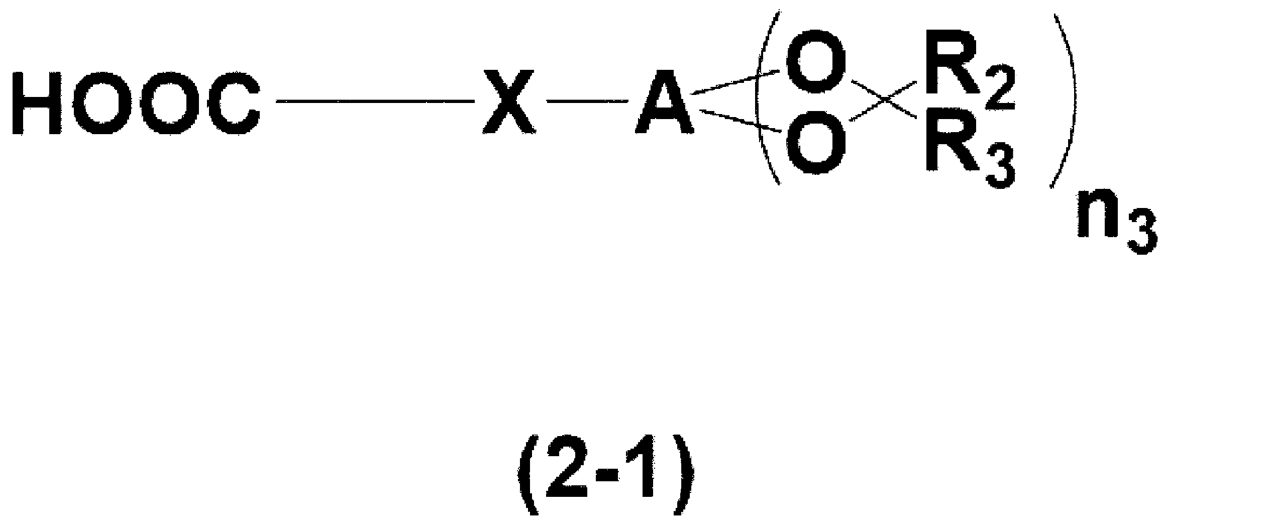
(上記式(2-1)中、Xは2価の有機基であり、Aは多環芳香族炭化水素基であり、R2及びR3は各々独立に水素原子、置換されてもよい炭素原子数1~10のアルキル基、置換されてもよい炭素原子数6~40のアリール基又はハロゲン原子であり、n3は1~12の整数である。
式(2-1)のカルボキシ基が、ヒドロキシ基、アシル基、アセチル基、ホルミル基、ベンゾイル基、カルボキシ基、カルボニル基、アミノ基、イミノ基、シアノ基、アゾ基、アジ基、チオール基、スルホ基及びアリル基に置き換わっていてもよい。
(In the above formula (2-1), X is a divalent organic group, A is a polycyclic aromatic hydrocarbon group, R 2 and R 3 are each independently a hydrogen atom, an optionally substituted carbon It is an alkyl group having 1 to 10 atoms, an aryl group having 6 to 40 carbon atoms which may be substituted, or a halogen atom, and n3 is an integer of 1 to 12.
The carboxy group of formula (2-1) is a hydroxy group, an acyl group, an acetyl group, a formyl group, a benzoyl group, a carboxy group, a carbonyl group, an amino group, an imino group, a cyano group, an azo group, an azide group, a thiol group, It may be substituted with a sulfo group and an allyl group.
上記Xの具体例としては、エステル結合、エーテル結合、アミド結合、ウレタン結合又はウレア結合である。
Specific examples of X above are an ester bond, an ether bond, an amide bond, a urethane bond, or a urea bond.
上記Aの具体例としては、ナフタレン、アントラセン、フェナントレン、又はピレンから誘導される基が挙げられる。
Specific examples of A above include groups derived from naphthalene, anthracene, phenanthrene, or pyrene.
上記ハロゲン原子としては、フッ素原子、塩素原子、臭素原子及びヨウ素原子が挙げられる。
The above halogen atoms include a fluorine atom, a chlorine atom, a bromine atom and an iodine atom.
上記アルキル基の具体例としては、メチル基、エチル基、プロピル基、ブチル基、ヘキシル基、ペンチル基等が挙げられる。
Specific examples of the above alkyl groups include methyl, ethyl, propyl, butyl, hexyl, and pentyl groups.
上記アルコキシ基の具体例としては、メトキシ基、エトキシ基、プロポキシ基、ブトキシ基、ヘキソキシ基、ペントキシ基等が挙げられる。
Specific examples of the alkoxy groups include methoxy, ethoxy, propoxy, butoxy, hexoxy, and pentoxy groups.
上記アリール基としては、フェニル基、ナフチル基等が挙げられる。
Examples of the aryl group include a phenyl group and a naphthyl group.
上記置換されていてもよいとは、上記アルキル基又はアルコキシ基の一部又は全部の水素原子が、例えば、フルオロ基又はヒドロキシ基で置換されていてもよいことをいう。
The "may be substituted" means that some or all of the hydrogen atoms in the alkyl group or alkoxy group may be substituted with, for example, a fluoro group or a hydroxy group.
国際公開第2020/071361号公報記載の全開示が、本願の参照として援用される。
The entire disclosure described in International Publication No. 2020/071361 is incorporated herein by reference.
[溶剤]
本発明に係る光硬化性樹脂組成物に含まれる溶剤としては、例えば、水、エチレングリコールモノメチルエーテル、エチレングリコールモノエチルエーテル、メチルセロソルブアセテート、エチルセロソルブアセテート、ジエチレングリコールモノメチルエーテル、ジエチレングリコールモノエチルエーテル、プロピレングリコール、プロピレングリコールモノメチルエーテル、プロピレングリコールモノエチルエーテル、プロピレングリコールモノメチルエーテルアセテート、プロピレングリコールプロピルエーテルアセテート、トルエン、キシレン、メチルエチルケトン、メチルイソブチルケトン、シクロペンタノン、シクロヘキサノン、シクロヘプタノン、4-メチル-2-ペンタノール、2-ヒドロキシイソ酪酸メチル、2-ヒドロキシイソ酪酸エチル、エトキシ酢酸エチル、酢酸2-ヒドロキシエチル、3-メトキシプロピオン酸メチル、3-メトキシプロピオン酸エチル、3-エトキシプロピオン酸エチル、3-エトキシプロピオン酸メチル、ピルビン酸メチル、ピルビン酸エチル、酢酸エチル、酢酸ブチル、乳酸エチル、乳酸ブチル、2-ヘプタノン、メトキシシクロペンタン、アニソール、γ-ブチロラクトン、N-メチルピロリドン、N,N-ジメチルホルムアミド、及びN,N-ジメチルアセトアミドが挙げられる。これらの溶剤は、単独で又は2種以上を組み合わせて用いることができる。 [solvent]
Examples of solvents contained in the photocurable resin composition according to the present invention include water, ethylene glycol monomethyl ether, ethylene glycol monoethyl ether, methyl cellosolve acetate, ethyl cellosolve acetate, diethylene glycol monomethyl ether, diethylene glycol monoethyl ether, and propylene. Glycol, propylene glycol monomethyl ether, propylene glycol monoethyl ether, propylene glycol monomethyl ether acetate, propylene glycol propyl ether acetate, toluene, xylene, methyl ethyl ketone, methyl isobutyl ketone, cyclopentanone, cyclohexanone, cycloheptanone, 4-methyl-2 -pentanol, methyl 2-hydroxyisobutyrate, ethyl 2-hydroxyisobutyrate, ethyl ethoxyacetate, 2-hydroxyethyl acetate, methyl 3-methoxypropionate, ethyl 3-methoxypropionate, ethyl 3-ethoxypropionate, 3 -methyl ethoxypropionate, methyl pyruvate, ethyl pyruvate, ethyl acetate, butyl acetate, ethyl lactate, butyl lactate, 2-heptanone, methoxycyclopentane, anisole, γ-butyrolactone, N-methylpyrrolidone, N,N-dimethyl Formamide, and N,N-dimethylacetamide. These solvents can be used alone or in combination of two or more.
これらの溶剤の中でプロピレングリコールモノメチルエーテル、プロピレングリコールモノメチルエーテルアセテート、乳酸エチル、乳酸ブチル、及びシクロヘキサノンが好ましい。特にプロピレングリコールモノメチルエーテル、プロピレングリコールモノメチルエーテルアセテートが好ましい。
Among these solvents, propylene glycol monomethyl ether, propylene glycol monomethyl ether acetate, ethyl lactate, butyl lactate, and cyclohexanone are preferred. Propylene glycol monomethyl ether and propylene glycol monomethyl ether acetate are particularly preferred.
溶剤は、本発明に係る光硬化性樹脂組成物が適度な粘度を有するように添加すればよい。一般的には多環芳香族炭化水素基を含有するポリマー又は化合物100質量部に対し、100~3,000質量部程度が好ましい。
The solvent should be added so that the photocurable resin composition according to the present invention has an appropriate viscosity. In general, it is preferably about 100 to 3,000 parts by mass with respect to 100 parts by mass of a polymer or compound containing a polycyclic aromatic hydrocarbon group.
本発明に係る多環芳香族炭化水素基を含有するポリマー及び/又は化合物は、光、電子線、その他の電磁波、ラジカル、酸、熱、水、酸素等の作用により架橋構造を形成し得る架橋性基(例えば、エポキシ基、アクリル基、ビニル基、カルボン酸基、チオール基、シラノール基、シンナモイル基、水酸基(フェノール性水酸基も含む)等)を有さなくても、多環芳香族炭化水素基に起因する光硬化を起こすことができる。
The polymer and/or compound containing a polycyclic aromatic hydrocarbon group according to the present invention is a crosslinked structure capable of forming a crosslinked structure by the action of light, electron beams, other electromagnetic waves, radicals, acids, heat, water, oxygen, or the like. polycyclic aromatic hydrocarbons (e.g., epoxy groups, acrylic groups, vinyl groups, carboxylic acid groups, thiol groups, silanol groups, cinnamoyl groups, hydroxyl groups (including phenolic hydroxyl groups), etc.). Photocuring due to radicals can occur.
また、本発明に係る光硬化性樹脂組成物は、特段の添加剤を配合しなくても、光硬化を起こすことができるが、必要に応じて、ラジカル重合開始剤(光重合開始剤など)、酸(触媒)、熱酸発生剤、光酸発生剤、塩基(触媒)、熱塩基発生剤、光塩基発生剤、酸化防止剤、重合禁止剤、架橋剤(多官能アクリルなど)、密着性向上剤、密着助剤(シランカップリング剤)、界面活性剤、消泡剤、レオロジー調整剤、顔料、染料、保存安定剤、多価フェノールや多価カルボン酸等の溶解促進剤、増感剤等を含めることができる。
In addition, the photocurable resin composition according to the present invention can be photocured without adding any special additives. , acid (catalyst), thermal acid generator, photoacid generator, base (catalyst), thermal base generator, photobase generator, antioxidant, polymerization inhibitor, cross-linking agent (polyfunctional acrylic, etc.), adhesion Improving agents, adhesion aids (silane coupling agents), surfactants, defoaming agents, rheology modifiers, pigments, dyes, storage stabilizers, dissolution accelerators such as polyhydric phenols and polyhydric carboxylic acids, sensitizers etc. can be included.
ラジカル重合開始剤は、光照射及び/又は加熱によりラジカル重合を開始させる物質を放出することが可能であればよい。例えば、光ラジカル重合開始剤としては、ベンゾフェノン誘導体、イミダゾール誘導体、ビスイミダゾール誘導体、N-アリールグリシン誘導体、有機アジド化合物、チタノセン化合物、アルミナート錯体、有機過酸化物、N-アルコキシピリジニウム塩、チオキサントン誘導体等が挙げられる。更に具体的には、ベンゾフェノン、1,3-ジ(tert-ブチルジオキシカルボニル)ベンゾフェノン、3,3’,4,4’-テトラキス(tert-ブチルジオキシカルボニル)ベンゾフェノン、3-フェニル-5-イソオキサゾロン、2-メルカプトベンズイミダゾール、ビス(2,4,5-トリフェニル)イミダゾール、2,2-ジメトキシ-1,2-ジフェニルエタン-1-オン、1-ヒドロキシシクロヘキシルフェニルケトン、2-ベンジル-2-ジメチルアミノ-1-(4-モルフォリノフェニル)-ブタン-1-オン、ビス(η5-2,4-シクロペンタジエン-1-イル)-ビス(2,6-ジフルオロ-3-(1H-ピロール-1-イル)-フェニル)チタニウム)等が挙げられるが、これらに限定されない。
Any radical polymerization initiator may be used as long as it can release a substance that initiates radical polymerization upon exposure to light and/or heat. Examples of photoradical polymerization initiators include benzophenone derivatives, imidazole derivatives, bisimidazole derivatives, N-arylglycine derivatives, organic azide compounds, titanocene compounds, aluminate complexes, organic peroxides, N-alkoxypyridinium salts, thioxanthone derivatives. etc. More specifically, benzophenone, 1,3-di(tert-butyldioxycarbonyl)benzophenone, 3,3′,4,4′-tetrakis(tert-butyldioxycarbonyl)benzophenone, 3-phenyl-5- isoxazolone, 2-mercaptobenzimidazole, bis(2,4,5-triphenyl)imidazole, 2,2-dimethoxy-1,2-diphenylethan-1-one, 1-hydroxycyclohexylphenyl ketone, 2-benzyl- 2-dimethylamino-1-(4-morpholinophenyl)-butan-1-one, bis(η 5 -2,4-cyclopentadien-1-yl)-bis(2,6-difluoro-3-(1H -pyrrol-1-yl)-phenyl)titanium) and the like, but are not limited thereto.
上記光ラジカル重合開始剤としては市販品を利用することもでき、例えば、BASF社製のIRGACURE(登録商標)651、184、369、784等が挙げられる。また、上記以外の市販品も使用でき、具体的には、BASF社製IRGACURE(登録商標)500、907、379、819、127、500、754、250、1800、1870、OXE01、DAROCUR(登録商標)TPO、1173;Lambson社製Speedcure(登録商標)MBB、PBZ、ITX、CTX、EDB;Lamberti社製Esacure(登録商標)ONE、KIP150、KTO46;日本化薬(株)製KAYACURE(登録商標)DETX-S、CTX、BMS、DMBI等が挙げられる
Commercially available products can be used as the radical photopolymerization initiator, and examples include IRGACURE (registered trademark) 651, 184, 369, 784 manufactured by BASF. In addition, commercial products other than the above can also be used. ) TPO, 1173; Speedcure (registered trademark) MBB, PBZ, ITX, CTX, EDB manufactured by Lambson; Esacure (registered trademark) ONE, KIP150, KTO46 manufactured by Lamberti; KAYACURE (registered trademark) DETX manufactured by Nippon Kayaku Co., Ltd. -S, CTX, BMS, DMBI, etc.
また、熱ラジカル重合開始剤としては、例えば、アセチルペルオキシド、ベンゾイルペルオキシド、メチルエチルケトンペルオキシド、シクロヘキサノンペルオキシド、過酸化水素、tert-ブチルヒドロペルオキシド、クメンヒドロペルオキシド、ジ-tert-ブチルペルオキシド、ジクミルペルオキシド、ジラウロイルペルオキシド、tert-ブチルペルオキシアセテート、tert-ブチルペルオキシピバラート、tert-ブチルぺルオキシ-2-エチルヘキサノアート等の過酸化物;2,2’-アゾビスイソブチロニトリル、2,2’-アゾビス(2,4-ジメチルバレロニトリル)、(1-フェニルエチル)アゾジフェニルメタン、2,2’-アゾビス(4-メトキシ-2,4-ジメチルバレロニトリル)、ジメチル-2,2’-アゾビスイソブチラート、2,2’-アゾビス(2-メチルブチロニトリル)、1,1’-アゾビス(1-シクロヘキサンカルボニトリル)、2-(カルバモイルアゾ)イソブチロニトリル、2,2’-アゾビス(2,4,4-トリメチルペンタン)、2-フェニルアゾ-2,4-ジメチル-4-メトキシバレロニトリル、2,2’-アゾビス(2-メチルプロパン)等のアゾ系化合物;過硫酸アンモニウム、過硫酸ナトリウム、過硫酸カリウム等の過硫酸塩等が挙げられるが、これらに限定されない。
Examples of thermal radical polymerization initiators include acetyl peroxide, benzoyl peroxide, methyl ethyl ketone peroxide, cyclohexanone peroxide, hydrogen peroxide, tert-butyl hydroperoxide, cumene hydroperoxide, di-tert-butyl peroxide, dicumyl peroxide, di Peroxides such as lauroyl peroxide, tert-butylperoxyacetate, tert-butylperoxypivalate, tert-butylperoxy-2-ethylhexanoate; 2,2'-azobisisobutyronitrile, 2,2' -azobis(2,4-dimethylvaleronitrile), (1-phenylethyl)azodiphenylmethane, 2,2'-azobis(4-methoxy-2,4-dimethylvaleronitrile), dimethyl-2,2'-azobis isobutyrate, 2,2′-azobis(2-methylbutyronitrile), 1,1′-azobis(1-cyclohexanecarbonitrile), 2-(carbamoylazo)isobutyronitrile, 2,2′-azobis Azo compounds such as (2,4,4-trimethylpentane), 2-phenylazo-2,4-dimethyl-4-methoxyvaleronitrile, 2,2′-azobis(2-methylpropane); ammonium persulfate, persulfate Examples include, but are not limited to, persulfates such as sodium and potassium persulfate.
市販の熱ラジカル重合開始剤としては、例えば、日油(株)製パーロイル(登録商標)IB、NPP、IPP、SBP、TCP、OPP、SA、355、L、パーブチル(登録商標)ND、NHP、MA、PV、355、A、C、D、E、L、I、O、P、Z、パーヘキシル(登録商標)ND、PV、D、I、O、Z、パーオクタ(登録商標)ND、ナイパー(登録商標)PMB、BMT、BW、パーテトラ(登録商標)A、パーヘキサ(登録商標)MC、TMH、HC、250、25B、C、25Z、22、V、パーオクタ(登録商標)O、パークミル(登録商標)ND、D、パーメンタ(登録商標)H、ノフマー(登録商標)BC;和光純薬(株)製V-70、V-65、V-59、V-40、V-30、VA-044、VA-046B、VA-061、V-50、VA-057、VA-086、VF-096、VAm-110、V-601、V-501;BASF社製IRGACURE(登録商標)184、369、651、500、819、907、784、2959、CGI1700、CGI1750、CGI1850、CG24-61、DAROCUR(登録商標)1116、1173、LUCIRIN(登録商標)TPO;サイテックサーフェイススペシャルティーズ社製UVECRYL(登録商標)P36;Lamberti社製Esacure(登録商標)KIP150、KIP65LT、KIP100F、KT37、KT55、KTO46、KIP75/B等が挙げられるが、これらに限定されない。
Examples of commercially available thermal radical polymerization initiators include NOF Corporation Perloyl (registered trademark) IB, NPP, IPP, SBP, TCP, OPP, SA, 355, L, Perbutyl (registered trademark) ND, NHP, MA, PV, 355, A, C, D, E, L, I, O, P, Z, Perhexyl (registered trademark) ND, PV, D, I, O, Z, Perocta (registered trademark) ND, Nyper ( Registered trademarks) PMB, BMT, BW, Pertetra (registered trademark) A, Perhexa (registered trademark) MC, TMH, HC, 250, 25B, C, 25Z, 22, V, Perocta (registered trademark) O, Percumyl (registered trademark) ) ND, D, Permenta (registered trademark) H, Nofmar (registered trademark) BC; Wako Pure Chemical Industries, Ltd. V-70, V-65, V-59, V-40, V-30, VA-044, VA-046B, VA-061, V-50, VA-057, VA-086, VF-096, VAm-110, V-601, V-501; BASF IRGACURE® 184, 369, 651, 500, 819, 907, 784, 2959, CGI1700, CGI1750, CGI1850, CG24-61, DAROCUR® 1116, 1173, LUCIRIN® TPO; Cytec Surface Specialties UVECRYL® P36; Lamberti Esacure (registered trademark) KIP150, KIP65LT, KIP100F, KT37, KT55, KTO46, KIP75/B, etc. manufactured by the company, but not limited thereto.
ラジカル重合開始剤は一種のみを使用してもよく、二種以上を併用してもよい。ラジカル重合開始剤の含有量は、環芳香族炭化水素基を含有するポリマー及び/又は化合物100質量部に対し、好ましくは1質量部以上、2質量部以上、3質量部以上、50質量部以下、20質量部以下、10質量部以下である。
Only one type of radical polymerization initiator may be used, or two or more types may be used in combination. The content of the radical polymerization initiator is preferably 1 part by mass or more, 2 parts by mass or more, 3 parts by mass or more and 50 parts by mass or less with respect to 100 parts by mass of the polymer and/or compound containing a ring aromatic hydrocarbon group. , 20 parts by mass or less, and 10 parts by mass or less.
触媒としては、酸性化合物、塩基性化合物、又は熱若しくは光により酸若しくは塩基が発生する各種化合物を用いることができる。
As the catalyst, acidic compounds, basic compounds, or various compounds that generate acid or base by heat or light can be used.
酸性化合物としては、スルホン酸化合物又はカルボン酸化合物を用いることができる。
スルホン酸化合物又はカルボン酸化合物として、例えば、p-トルエンスルホン酸、トリフルオロメタンスルホン酸、ピリジニウムトリフルオロメタンスルホナート(=ピリジニウムトリフルオロメタンスルホン酸)、ピリジニウム-p-トルエンスルホネート、ピリジニウム-4-ヒドロキシベンゼンスルホナート、サリチル酸、カンファースルホン酸、5-スルホサリチル酸、4-クロロベンゼンスルホン酸、4-フェノールスルホン酸、ピリジニウム-4-フェノールスルホネート、ベンゼンジスルホン酸、1-ナフタレンスルホン酸、4-ニトロベンゼンスルホン酸、クエン酸、安息香酸、ヒドロキシ安息香酸が挙げられる。 A sulfonic acid compound or a carboxylic acid compound can be used as the acidic compound.
Sulfonic acid compounds or carboxylic acid compounds such as p-toluenesulfonic acid, trifluoromethanesulfonic acid, pyridinium trifluoromethanesulfonate (=pyridinium trifluoromethanesulfonic acid), pyridinium-p-toluenesulfonate, pyridinium-4-hydroxybenzenesulfonate phosphate, salicylic acid, camphorsulfonic acid, 5-sulfosalicylic acid, 4-chlorobenzenesulfonic acid, 4-phenolsulfonic acid, pyridinium-4-phenolsulfonate, benzenedisulfonic acid, 1-naphthalenesulfonic acid, 4-nitrobenzenesulfonic acid, citric acid , benzoic acid, and hydroxybenzoic acid.
塩基性化合物としては、アミン化合物又は水酸化アンモニウム化合物を用いることができ、熱により塩基が発生する化合物としては、尿素を用いることができる。
アミン化合物として、例えば、トリエタノールアミン、トリブタノールアミン、トリメチルアミン、トリエチルアミン、トリノルマルプロピルアミン、トリイソプロピルアミン、トリノルマルブチルアミン、トリ-tert-ブチルアミン、トリノルマルオクチルアミン、トリイソプロパノールアミン、フェニルジエタノールアミン、ステアリルジエタノールアミン、及びジアザビシクロオクタン等の第3級アミン、ピリジン及び4-ジメチルアミノピリジン等の芳香族アミンが挙げられる。また、ベンジルアミン及びノルマルブチルアミン等の第1級アミン、ジエチルアミン及びジノルマルブチルアミン等の第2級アミンもアミン化合物として挙げられる。
水酸化アンモニウム化合物としては、例えば、水酸化テトラメチルアンモニウム、水酸化テトラエチルアンモニウム、水酸化テトラプロピルアンモニウム、水酸化テトラブチルアンモニウム、水酸化ベンジルトリメチルアンモニウム、水酸化ベンジルトリエチルアンモニウム、水酸化セチルトリメチルアンモニウム、水酸化フェニルトリメチルアンモニウム、水酸化フェニルトリエチルアンモニウムが挙げられる。 An amine compound or an ammonium hydroxide compound can be used as the basic compound, and urea can be used as the compound that generates a base by heat.
Examples of amine compounds include triethanolamine, tributanolamine, trimethylamine, triethylamine, tri-n-propylamine, tri-isopropylamine, tri-n-butylamine, tri-tert-butylamine, tri-n-octylamine, triisopropanolamine, phenyldiethanolamine, stearyl Tertiary amines such as diethanolamine and diazabicyclooctane, aromatic amines such as pyridine and 4-dimethylaminopyridine. Amine compounds also include primary amines such as benzylamine and n-butylamine, and secondary amines such as diethylamine and di-n-butylamine.
Examples of ammonium hydroxide compounds include tetramethylammonium hydroxide, tetraethylammonium hydroxide, tetrapropylammonium hydroxide, tetrabutylammonium hydroxide, benzyltrimethylammonium hydroxide, benzyltriethylammonium hydroxide, cetyltrimethylammonium hydroxide, phenyltrimethylammonium hydroxide and phenyltriethylammonium hydroxide.
酸発生剤としては、熱酸発生剤、光酸発生剤何れも使用することができる。
Both thermal acid generators and photoacid generators can be used as acid generators.
熱酸発生剤としては、例えば、p-トルエンスルホン酸、トリフルオロメタンスルホン酸、ピリジニウム-p-トルエンスルホネート(ピリジニウム-p-トルエンスルホン酸)、ピリジニウム-p-ヒドロキシベンゼンスルホン酸(p-フェノールスルホン酸ピリジニウム塩)、ピリジニウム-トリフルオロメタンスルホン酸、サリチル酸、カンファースルホン酸、5-スルホサリチル酸、4-クロロベンゼンスルホン酸、4-ヒドロキシベンゼンスルホン酸、ベンゼンジスルホン酸、1-ナフタレンスルホン酸、クエン酸、安息香酸、ヒドロキシ安息香酸等のスルホン酸化合物及びカルボン酸化合物が挙げられる。
市販品としては、例えば、K-PURE〔登録商標〕CXC-1612、同CXC-1614、同TAG-2172、同TAG-2179、同TAG-2678、同TAG2689(以上、King Industries社製)、及びSI-45、SI-60、SI-80、SI-100、SI-110、SI-150(以上、三新化学工業株式会社製)が挙げられる。 Thermal acid generators include, for example, p-toluenesulfonic acid, trifluoromethanesulfonic acid, pyridinium-p-toluenesulfonate (pyridinium-p-toluenesulfonic acid), pyridinium-p-hydroxybenzenesulfonic acid (p-phenolsulfonic acid pyridinium salt), pyridinium-trifluoromethanesulfonic acid, salicylic acid, camphorsulfonic acid, 5-sulfosalicylic acid, 4-chlorobenzenesulfonic acid, 4-hydroxybenzenesulfonic acid, benzenedisulfonic acid, 1-naphthalenesulfonic acid, citric acid, benzoic acid and sulfonic acid compounds such as hydroxybenzoic acid and carboxylic acid compounds.
Commercially available products include, for example, K-PURE (registered trademark) CXC-1612, CXC-1614, TAG-2172, TAG-2179, TAG-2678, and TAG2689 (manufactured by King Industries), and SI-45, SI-60, SI-80, SI-100, SI-110, SI-150 (manufactured by Sanshin Chemical Industry Co., Ltd.).
光酸発生剤としてはスルホニウム塩、ヨードニウム塩、スルホニルジアゾメタン、N-スルホニルオキシイミド、ベンゾインスルホネート型光酸発生剤、ピロガロールトリスルホネート型光酸発生剤、スルホン型光酸発生剤、グリオキシム誘導体型光酸発生剤、オキシム-O-スルホネート型酸発生剤、ビスオキシムスルホネート型酸発生剤等がある。例えば、ビス(4-tert-ブチルフェニル)ヨードニウムトリフルオロメタンスルホネート、トリフェニルスルホニウムトリフルオロメタンスルホネート、フェニル-ビス(トリクロロメチル)-s-トリアジン、ベンゾイントシレート、及びN-ヒドロキシスクシンイミドトリフルオロメタンスルホネート等を挙げることができる。
Examples of photoacid generators include sulfonium salts, iodonium salts, sulfonyldiazomethanes, N-sulfonyloxyimides, benzoinsulfonate-type photoacid generators, pyrogallol trisulfonate-type photoacid generators, sulfone-type photoacid generators, and glyoxime derivative-type photoacid generators. generators, oxime-O-sulfonate type acid generators, bisoxime sulfonate type acid generators and the like. Examples include bis(4-tert-butylphenyl)iodonium trifluoromethanesulfonate, triphenylsulfonium trifluoromethanesulfonate, phenyl-bis(trichloromethyl)-s-triazine, benzoin tosylate, and N-hydroxysuccinimide trifluoromethanesulfonate. be able to.
これら酸発生剤は単独で用いることも2種類以上組み合わせて用いることもできる。光酸発生剤の含有量は、環芳香族炭化水素基を含有するポリマー及び/又は化合物100重量部に対して1~100重量部であることが好ましい。
These acid generators can be used alone or in combination of two or more. The content of the photoacid generator is preferably 1 to 100 parts by weight with respect to 100 parts by weight of the polymer and/or compound containing a ring aromatic hydrocarbon group.
熱塩基発生剤としては、例えば、1-メチル-1-(4-ビフェニリル)エチルカルバメート、2-シアノ-1,1-ジメチルエチルカルバメート等のカルバメート類;尿素、N,N-ジメチル-N’-メチル尿素等の尿素類;トリクロロ酢酸グアニジン、フェニルスルホニル酢酸グアニジン、フェニルプロピオール酸グアニジン等のグアニジン類;1,4-ジヒドロニコチンアミド等のジヒドロピリジン類;N-(イソプロポキシカルボニル)-2,6-ジメチルピペリジン、N-(tert-ブトキシカルボニル)-2,6-ジメチルピペリジン、N-(ベンジルオキシカルボニル)-2,6-ジメチルピペリジン等のジメチルピペリジン類;フェニルスルホニル酢酸テトラメチルアンモニウム、フェニルプロピオール酸テトラメチルアンモニウム等の四級化アンモニウム塩;ジシアンジアミドなどが挙げられる。また、1,8-ジアザビシクロ[5.4.0]ウンデカ-7-エン(DBU)の塩である、U-CAT(登録商標)SA810、同SA831、同SA841、同SA851[以上、サンアプロ(株)製]等が挙げられる。
Examples of thermal base generators include carbamates such as 1-methyl-1-(4-biphenylyl)ethylcarbamate and 2-cyano-1,1-dimethylethylcarbamate; urea, N,N-dimethyl-N'- ureas such as methylurea; guanidines such as guanidine trichloroacetate, guanidine phenylsulfonylacetate and guanidine phenylpropiolate; dihydropyridines such as 1,4-dihydronicotinamide; N-(isopropoxycarbonyl)-2,6-dimethyl Dimethylpiperidines such as piperidine, N-(tert-butoxycarbonyl)-2,6-dimethylpiperidine, N-(benzyloxycarbonyl)-2,6-dimethylpiperidine; tetramethylammonium phenylsulfonylacetate, tetramethylphenylpropiolate quaternary ammonium salts such as ammonium; dicyandiamide; In addition, U-CAT (registered trademark) SA810, SA831, SA841, SA851, which are salts of 1,8-diazabicyclo[5.4.0]undec-7-ene (DBU) [the above, San-Apro Co., Ltd. ) made] and the like.
光塩基発生剤としては、例えば、9-アントリルメチル=N,N-ジエチルカルバメート等のアルキルアミン系光塩基発生剤;9-アントリル=N,N-ジシクロヘキシルカルバメート、1-(9,10-アントラキノン-2-イル)エチル=N,N-ジシクロヘキシルカルバメート、ジシクロヘキシルアンモニウム=2-(3-ベンゾイルフェニル)プロピオネート、9-アントリル=N-シクロヘキシルカルバメート、1-(9,10-アントラキノン-2-イル)エチル=N-シクロヘキシルカルバメート、シクロヘキシルアンモニウム=2-(3-ベンゾイルフェニル)プロピオネート、(E)-N-シクロヘキシル-3-(2-ヒドロキシフェニル)アクリルアミド等のシクロアルキルアミン系光塩基発生剤;9-アントリルメチル=ピペリジン-1-カルボキシレート、(E)-1-ピペリジノ-3-(2-ヒドロキシフェニル)-2-プロペン-1-オン、(2-ニトロフェニル)メチル=4-ヒドロキシピペリジン-1-カルボキシレート、(2-ニトロフェニル)メチル=4-(メタクリロイルオキシ)ピペリジン-1-カルボキシレート等のピペリジン系光塩基発生剤;グアニジニウム=2-(3-ベンゾイルフェニル)プロピオネート、1,2-ジイソプロピル-3-(ビス(ジメチルアミノ)メチレン)グアニジニウム=2-(3-ベンゾイルフェニル)プロピオネート、1,2-ジシクロヘキシル-4,4,5,5-テトラメチルビグアニジウム=n-ブチルトリフェニルボラート、1,5,7-トリアザビシクロ[4.4.0]デカ-5-エニウム=2-(9-オキソキサンテン-2-イル)プロピオネート等のグアニジン系光塩基発生剤;1-(9,10-アントラキノン-2-イル)エチル=イミダゾール-1-カルボキシレート等のイミダゾール系光塩基発生剤等が挙げられる。
Examples of photobase generators include alkylamine photobase generators such as 9-anthrylmethyl=N,N-diethylcarbamate; 9-anthryl=N,N-dicyclohexylcarbamate, 1-(9,10-anthraquinone -2-yl)ethyl N,N-dicyclohexylcarbamate, dicyclohexylammonium 2-(3-benzoylphenyl)propionate, 9-anthryl N-cyclohexylcarbamate, 1-(9,10-anthraquinon-2-yl)ethyl = N-cyclohexylcarbamate, cyclohexylammonium = 2-(3-benzoylphenyl)propionate, (E)-N-cyclohexyl-3-(2-hydroxyphenyl)acrylamide, and other cycloalkylamine photobase generators; tolylmethyl piperidine-1-carboxylate, (E)-1-piperidino-3-(2-hydroxyphenyl)-2-propen-1-one, (2-nitrophenyl)methyl 4-hydroxypiperidine-1- Piperidine-based photobase generators such as carboxylate, (2-nitrophenyl)methyl = 4-(methacryloyloxy)piperidine-1-carboxylate; guanidinium = 2-(3-benzoylphenyl)propionate, 1,2-diisopropyl- 3-(bis(dimethylamino)methylene)guanidinium = 2-(3-benzoylphenyl)propionate, 1,2-dicyclohexyl-4,4,5,5-tetramethylbiguanidinium = n-butyltriphenylborate, Guanidine-based photobase generators such as 1,5,7-triazabicyclo[4.4.0]dec-5-enium 2-(9-oxoxanthen-2-yl)propionate; 1-(9,10 -anthraquinon-2-yl)ethyl=imidazole-1-carboxylate and other imidazole-based photobase generators.
これら光塩基発生剤は光酸発生剤と同様に、単独で用いることも、2種類以上組み合わせて用いることもできる。また、その含有量は、環芳香族炭化水素基を含有するポリマー及び/又は化合物100重量部に対して1~100重量部であることが好ましい。
These photobase generators can be used alone or in combination of two or more types, like the photoacid generators. Also, the content thereof is preferably 1 to 100 parts by weight with respect to 100 parts by weight of the polymer and/or compound containing a ring aromatic hydrocarbon group.
重合禁止剤としては、ヒンダードフェノール化合物を使用してもよく、具体的には2,6-ジイソブチルフェノール、3,5-ジ-t-ブチルフェノール、3,5-ジ-t-ブチルクレゾール、ハイドロキノン、ハイドロキノンモノメチルエーテル、N-ニトロソ-N-フェニルヒドロキシルアミンアルミニウム、ピロガロール、t-ブチルカテコール、4-メトキシ-1-ナフトール、2,6-ジ-t-ブチル-4-メチルフェノール、2,5-ジ-t-ブチル-ハイドロキノン、オクタデシル-3-(3,5-ジ-t-ブチル-4-ヒドロキシフェニル)プロピオネ-ト、イソオクチル-3-(3,5-ジ-t-ブチル-4-ヒドロキシフェニル)プロピオネート、4、4’-メチレンビス(2、6-ジ-t-ブチルフェノール)、4,4’-チオ-ビス(3-メチル-6-t-ブチルフェノール)、4,4’-ブチリデン-ビス(3-メチル-6-t-ブチルフェノール)、トリエチレングリコール-ビス〔3-(3-t-ブチル-5-メチル-4-ヒドロキシフェニル)プロピオネート〕、1,6-ヘキサンジオール-ビス〔3-(3,5-ジ-t-ブチル-4-ヒドロキシフェニル)プロピオネート〕、2,2-チオ-ジエチレンビス〔3-(3,5-ジ-t-ブチル-4-ヒドロキシフェニル)プロピオネート〕、N,N’ヘキサメチレンビス(3,5-ジ-t-ブチル-4-ヒドロキシ-ヒドロシンナマミド)、2,2’-メチレン-ビス(4-メチル-6-t-ブチルフェノール)、2,2’-メチレン-ビス(4-エチル-6-t-ブチルフェノール)、ペンタエリスリチル-テトラキス〔3-(3,5-ジ-t-ブチル-4-ヒドロキシフェニル)プロピオネート〕、トリス-(3,5-ジ-t-ブチル-4-ヒドロキシベンジル)-イソシアヌレイト、1,3,5-トリメチル-2,4,6-トリス(3,5-ジ-t-ブチル-4-ヒドロキシベンジル)ベンゼン、1,3,5-トリス(3-ヒドロキシ-2,6-ジメチル-4-イソプロピルベンジル)-1,3,5-トリアジン-2,4,6-(1H,3H,5H)-トリオン、1,3,5-トリス(4-t-ブチル-3-ヒドロキシ-2,6-ジメチルベンジル)-1,3,5-トリアジン-2,4,6-(1H,3H,5H)-トリオン、1,3,5-トリス(4-s-ブチル-3-ヒドロキシ-2,6-ジメチルベンジル)-1,3,5-トリアジン-2,4,6-(1H,3H,5H)-トリオン、1,3,5-トリス[4-(1-エチルプロピル)-3-ヒドロキシ-2,6-ジメチルベンジル]-1,3,5-トリアジン-2,4,6-(1H,3H,5H)-トリオン、1,3,5-トリス[4-トリエチルメチル-3-ヒドロキシ-2,6-ジメチルベンジル]-1,3,5-トリアジン-2,4,6-(1H,3H,5H)-トリオン、1,3,5-トリス(3-ヒドロキシ-2,6-ジメチル-4-フェニルベンジル)-1,3,5-トリアジン-2,4,6-(1H,3H,5H)-トリオン、1,3,5-トリス(4-t-ブチル-3-ヒドロキシ-2,5,6-トリメチルベンジル)-1,3,5-トリアジン-2,4,6-(1H,3H,5H)-トリオン、1,3,5-トリス(4-t-ブチル-5-エチル-3-ヒドロキシ-2,6-ジメチルベンジル)-1,3,5-トリアジン-2,4,6-(1H,3H,5H)-トリオン、1,3,5-トリス(4-t-ブチル-6-エチル-3-ヒドロキシ-2-メチルベンジル)-1,3,5-トリアジン-2,4,6-(1H,3H,5H)-トリオン、1,3,5-トリス(4-t-ブチル-6-エチル-3-ヒドロキシ-2,5-ジメチルベンジル)-1,3,5-トリアジン-2,4,6-(1H,3H,5H)-トリオン、1,3,5-トリス(4-t-ブチル-5,6-ジエチル-3-ヒドロキシ-2-メチルベンジル)-1,3,5-トリアジン-2,4,6-(1H,3H,5H)-トリオン、1,3,5-トリス(4-t-ブチル-3-ヒドロキシ-2-メチルベンジル)-1,3,5-トリアジン-2,4,6-(1H,3H,5H)-トリオン、1,3,5-トリス(4-t-ブチル-3-ヒドロキシ-2,5-ジメチルベンジル)-1,3,5-トリアジン-2,4,6-(1H,3H,5H)-トリオン、1,3,5-トリス(4-t-ブチル-5‐エチル-3-ヒドロキシ-2-メチルベンジル)-1,3,5-トリアジン-2,4,6-(1H,3H,5H)-トリオン等を挙げることができる。
ヒンダードフェノール化合物の中でも、1,3,5-トリス(4-t-ブチル-3-ヒドロキシ-2,6-ジメチルベンジル)-1,3,5-トリアジン-2,4,6-(1H,3H,5H)-トリオンが好ましい。
上記重合禁止剤は市販品を使用してもよく、具体例としてはIrganox-3114(BASFジャパン株式会社製)が挙げられる。 As the polymerization inhibitor, a hindered phenol compound may be used, specifically 2,6-diisobutylphenol, 3,5-di-t-butylphenol, 3,5-di-t-butylcresol, hydroquinone. , hydroquinone monomethyl ether, N-nitroso-N-phenylhydroxylamine aluminum, pyrogallol, t-butylcatechol, 4-methoxy-1-naphthol, 2,6-di-t-butyl-4-methylphenol, 2,5- Di-t-butyl-hydroquinone, Octadecyl-3-(3,5-di-t-butyl-4-hydroxyphenyl)propionate, Isooctyl-3-(3,5-di-t-butyl-4-hydroxy phenyl)propionate, 4,4'-methylenebis(2,6-di-t-butylphenol), 4,4'-thio-bis(3-methyl-6-t-butylphenol), 4,4'-butylidene-bis (3-methyl-6-t-butylphenol), triethylene glycol-bis [3-(3-t-butyl-5-methyl-4-hydroxyphenyl) propionate], 1,6-hexanediol-bis [3- (3,5-di-t-butyl-4-hydroxyphenyl)propionate], 2,2-thio-diethylenebis[3-(3,5-di-t-butyl-4-hydroxyphenyl)propionate], N , N′ hexamethylenebis(3,5-di-t-butyl-4-hydroxy-hydrocinnamamide), 2,2′-methylene-bis(4-methyl-6-t-butylphenol), 2,2 '-methylene-bis(4-ethyl-6-t-butylphenol), pentaerythrityl-tetrakis[3-(3,5-di-t-butyl-4-hydroxyphenyl)propionate], tris-(3,5 -di-t-butyl-4-hydroxybenzyl)-isocyanurate, 1,3,5-trimethyl-2,4,6-tris(3,5-di-t-butyl-4-hydroxybenzyl)benzene, 1,3,5-tris(3-hydroxy-2,6-dimethyl-4-isopropylbenzyl)-1,3,5-triazine-2,4,6-(1H,3H,5H)-trione, 1, 3,5-tris(4-t-butyl-3-hydroxy-2,6-dimethylbenzyl)-1,3,5-triazine-2,4,6-(1H,3H,5H)-trione, 1, 3,5-tris(4-s-butyl-3-hydroxy-2,6-dimethylbenzyl)-1,3,5-triazine-2,4,6-(1H,3H,5H)-trione, 1, 3,5-tris[4-(1-ethylpropyl)-3-hydroxy-2,6-dimethylbenzyl]-1,3,5-triazine-2,4,6-(1H,3H,5H)-trione , 1,3,5-tris[4-triethylmethyl-3-hydroxy-2,6-dimethylbenzyl]-1,3,5-triazine-2,4,6-(1H,3H,5H)-trione, 1,3,5-tris(3-hydroxy-2,6-dimethyl-4-phenylbenzyl)-1,3,5-triazine-2,4,6-(1H,3H,5H)-trione, 1, 3,5-tris(4-t-butyl-3-hydroxy-2,5,6-trimethylbenzyl)-1,3,5-triazine-2,4,6-(1H,3H,5H)-trione, 1,3,5-tris(4-t-butyl-5-ethyl-3-hydroxy-2,6-dimethylbenzyl)-1,3,5-triazine-2,4,6-(1H,3H,5H )-trione, 1,3,5-tris(4-t-butyl-6-ethyl-3-hydroxy-2-methylbenzyl)-1,3,5-triazine-2,4,6-(1H,3H ,5H)-trione, 1,3,5-tris(4-t-butyl-6-ethyl-3-hydroxy-2,5-dimethylbenzyl)-1,3,5-triazine-2,4,6- (1H,3H,5H)-trione, 1,3,5-tris(4-t-butyl-5,6-diethyl-3-hydroxy-2-methylbenzyl)-1,3,5-triazine-2, 4,6-(1H,3H,5H)-trione, 1,3,5-tris(4-t-butyl-3-hydroxy-2-methylbenzyl)-1,3,5-triazine-2,4, 6-(1H,3H,5H)-trione, 1,3,5-tris(4-t-butyl-3-hydroxy-2,5-dimethylbenzyl)-1,3,5-triazine-2,4, 6-(1H,3H,5H)-trione, 1,3,5-tris(4-t-butyl-5-ethyl-3-hydroxy-2-methylbenzyl)-1,3,5-triazine-2, 4,6-(1H,3H,5H)-trione and the like can be mentioned.
Among hindered phenol compounds, 1,3,5-tris(4-t-butyl-3-hydroxy-2,6-dimethylbenzyl)-1,3,5-triazine-2,4,6-(1H, 3H,5H)-trione is preferred.
A commercial product may be used as the polymerization inhibitor, and a specific example thereof is Irganox-3114 (manufactured by BASF Japan Ltd.).
重合禁止剤は一種のみを使用してもよく、二種以上を併用してもよい。重合禁止剤の含有量は、環芳香族炭化水素基を含有するポリマー及び/又は化合物100質量部に対し、0.01~1質量部が好ましく、0.01~0.5質量部がより好ましい。
Only one type of polymerization inhibitor may be used, or two or more types may be used in combination. The content of the polymerization inhibitor is preferably 0.01 to 1 part by mass, more preferably 0.01 to 0.5 parts by mass, with respect to 100 parts by mass of the polymer and/or compound containing a ring aromatic hydrocarbon group. .
界面活性剤としては、例えば、ポリオキシエチレンラウリルエーテル、ポリオキシエチレンステアリルエーテル及びポリオキシエチレンオレイルエーテル等のポリオキシエチレンアルキルエーテル化合物、ポリオキシエチレンオクチルフェノールエーテル及びポリオキシエチレンノニルフェノールエーテル等のポリオキシエチレンアルキルアリルエーテル化合物、ポリオキシエチレン・ポリオキシプロピレンブロックコポリマー化合物、ソルビタンモノラウレート、ソルビタンモノパルミテート、ソルビタンモノステアレート、ソルビタントリオレエート及びソルビタントリステアレート等のソルビタン脂肪酸エステル化合物、ポリオキシエチレンソルビタンモノラウレート、ポリオキシエチレンソルビタンモノパルミテート、ポリオキシエチレンソルビタンモノステアレート及びポリオキシエチレンソルビタントリステアレート等のポリオキシエチレンソルビタン脂肪酸エステル化合物が挙げられる。また、商品名エフトップEF301,EF303、EF352((株)トーケムプロダクツ製)、商品名メガファックF171、F173、R-08、R-30(大日本インキ(株)製)、フロラードFC430、FC431(住友スリーエム(株)製)、商品名アサヒガードAG710,サーフロンS-382、SC101、SC102、SC103、SC104、SC105、SC106(旭硝子(株)製)等のフッ素系界面活性剤及びオルガノシロキサンポリマ-KP341(信越化学工業(株)製)等を上げることができる。
Examples of surfactants include polyoxyethylene alkyl ether compounds such as polyoxyethylene lauryl ether, polyoxyethylene stearyl ether and polyoxyethylene oleyl ether, and polyoxyethylene compounds such as polyoxyethylene octylphenol ether and polyoxyethylene nonylphenol ether. Alkyl allyl ether compounds, polyoxyethylene/polyoxypropylene block copolymer compounds, sorbitan fatty acid ester compounds such as sorbitan monolaurate, sorbitan monopalmitate, sorbitan monostearate, sorbitan trioleate and sorbitan tristearate, polyoxyethylene sorbitan polyoxyethylene sorbitan fatty acid ester compounds such as monolaurate, polyoxyethylene sorbitan monopalmitate, polyoxyethylene sorbitan monostearate and polyoxyethylene sorbitan tristearate; Also, trade names Ftop EF301, EF303, EF352 (manufactured by Tochem Products Co., Ltd.), trade names Megafac F171, F173, R-08, R-30 (manufactured by Dainippon Ink Co., Ltd.), Florard FC430, FC431 (manufactured by Sumitomo 3M Co., Ltd.), product names Asahiguard AG710, Surflon S-382, SC101, SC102, SC103, SC104, SC105, SC106 (manufactured by Asahi Glass Co., Ltd.) and other fluorine-based surfactants and organosiloxane polymers. KP341 (manufactured by Shin-Etsu Chemical Co., Ltd.) and the like can be mentioned.
界面活性剤は一種のみを使用してもよく、二種以上を併用してもよい。界面活性剤の含有量は、環芳香族炭化水素基を含有するポリマー及び/又は化合物100質量部に対し、好ましくは0.1質量部以上、0.5質量部以上、5質量部以下、2質量部以下である。
Only one type of surfactant may be used, or two or more types may be used in combination. The content of the surfactant is preferably 0.1 parts by mass or more, 0.5 parts by mass or more, and 5 parts by mass or less with respect to 100 parts by mass of the polymer and/or compound containing a ring aromatic hydrocarbon group. Part by mass or less.
また、現像後の基板との密着性を向上させる目的で、密着促進剤を含有することもできる。このような密着促進剤の具体例としては、例えばトリメチルクロロシラン、ジメチルビニルクロロシラン、メチルジフェニルクロロシラン、クロロメチルジメチルクロロシラン等のクロロシラン類、トリメチルメトキシシラン、ジメチルジエトキシシラン、メチルジメトキシシラン、ジメチルビニルエトキシシラン、ジフェニルジメトキシシラン、フェニルトリエトキシシラン等のアルコキシシラン類、ヘキサメチルジシラザン、N,N’-ビス(トリメチルシリル)ウレア、ジメチルトリメチルシリルアミン、トリメチルシリルイミダゾール類のシラザン類、ビニルトリクロロシラン、γ-クロロプロピルトリメトキシシラン、γ-アミノプロピルトリエトキシシラン、γ-メタクリロキシプロピルトリメトキシシラン、γ-グリシドキシプロピルトリメトキシシラン等のシラン類、ベンゾトリアゾール、ベンズイミダゾール、インダゾール、イミダゾール、2-メルカプトベンズイミダゾール、2-メルカプトベンゾチアゾール、2-メルカプトベンゾオキサゾール、ウラゾール、チオウラシル、メルカプトイミダゾール、メルカプトピリミジン等の複素環状化合物や、1,1-ジメチレンウレア、1,3-ジメチルウレア等の尿素、またはチオ尿素化合物を挙げることができる。
In addition, an adhesion promoter can be included for the purpose of improving the adhesion to the substrate after development. Specific examples of such adhesion promoters include chlorosilanes such as trimethylchlorosilane, dimethylvinylchlorosilane, methyldiphenylchlorosilane, chloromethyldimethylchlorosilane, trimethylmethoxysilane, dimethyldiethoxysilane, methyldimethoxysilane, and dimethylvinylethoxysilane. , diphenyldimethoxysilane, phenyltriethoxysilane and other alkoxysilanes, hexamethyldisilazane, N,N'-bis(trimethylsilyl)urea, dimethyltrimethylsilylamine, trimethylsilylimidazole silazanes, vinyltrichlorosilane, γ-chloropropyl Silanes such as trimethoxysilane, γ-aminopropyltriethoxysilane, γ-methacryloxypropyltrimethoxysilane, γ-glycidoxypropyltrimethoxysilane, benzotriazole, benzimidazole, indazole, imidazole, 2-mercaptobenzimidazole , 2-mercaptobenzothiazole, 2-mercaptobenzoxazole, urazole, thiouracil, mercaptoimidazole, mercaptopyrimidine and other heterocyclic compounds, ureas such as 1,1-dimethylurea and 1,3-dimethylurea, or thiourea compounds can be mentioned.
これらの密着促進剤の配合量は、環芳香族炭化水素基を含有するポリマー及び/又は化合物100重量部に対して、通常、20重量部以下、好ましくは0.05~10重量部、特に好ましくは1~10重量部である。
The amount of these adhesion promoters is usually 20 parts by weight or less, preferably 0.05 to 10 parts by weight, particularly preferably 0.05 to 10 parts by weight, per 100 parts by weight of the polymer and/or compound containing a ring aromatic hydrocarbon group. is 1 to 10 parts by weight.
染料としては、酸性染料、油溶性染料、分散染料、反応性染料、直接染料等が挙げられる。例えば、アゾ系染料、ベンゾキノン系染料、ナフトキノン系染料、アントラキノン系染料、シアニン系染料、スクアリリウム系染料、クロコニウム系染料、メロシアニン系染料、スチルベン系染料、ジフェニルメタン系染料、トリフェニルメタン系染料、フルオラン系染料、スピロピラン系染料、フタロシアニン系染料、インジゴ系染料、フルギド系染料、ニッケル錯体系染料、及びアズレン系染料が挙げられる。具体的には、カラーインデックス番号で以下のものが挙げられる。C.I.Solvent Yellow2、3、7、12、13、14、16、18、19、21、25、25:1、27、28、29、30、33、34、36、42、43、44、47、56、62、72、73、77、79、81、82、83、83:1、88、89、90、93、94、96、98、104、107、114、116、117、124、130、131、133、135、141、143、145、146、157、160:1、161、162、163、167、169、172、174、175、176、179、180、181、182、183、184、185、186、187、189、190、191、C.I.Solvent Orange1、2、3、4、5、7、11、14、20、23、25、31、40:1、41、45、54、56、58、60、62、63、70、75、77、80、81、86、99、102、103、105、106、107、108、109、110、111、112、113、C.I.Solvent Red1、2、3、4、8、16、17、18、19、23、24、25、26、27、30、33、35、41、43、45、48、49、52、68、69、72、73、83:1、84:1、89、90、90:1、91、92、106、109、110、118、119、122、124、125、127、130、132、135、141、143、145、146、149、150、151、155、160、161、164、164:1、165、166、168、169、172、175、179、180、181、182、195、196、197、198、207、208、210、212、214、215、218、222、223、225、227、229、230、233、234、235、236、238、239、240、241、242、243、244、245、247、248、C.I.Solvent Violet2、8、9、11、13、14、21、21:1、26、31、36、37、38、45、46、47、48、49、50、51、55、56、57、58、59、60、61、C.I.Solvent Blue2、3、4、5、7、18、25、26、35、36、37、38、43、44、45、48、51、58、59、59:1、63、64、67、68、69、70、78、79、83、94、97、98、100、101、102、104、105、111、112、122、124、128、129、132、136、137、138、139、143、C.I.Solvent Green1、3、4、5、7、28、29、32、33、34、35、C.I.Solvent Brown1、3、4、5、12、20、22、28、38、41、42、43、44、52、53、59、60、61、62、63、C.I.Solvent Black3、5、5:2、7、13、22、22:1、26、27、28、29、34、35、43、45、46、48、49、50、C.I.Acid Red 6、11、26、60、88、111、186、215、C.I.Acid Green 25、27、C.I.Acid Blue 22、25、40、78、92、113、129、167、230、C.I.Acid Yellow 17、23、25、36、38、42、44、72、78、C.I.Basic Red 1、2、13、14、22、27、29、39、C.I.Basic Green 3、4、C.I.Basic Blue 3、9、41、66、C.I.Basic Violet 1、3、18、39、66、C.I.Basic Yellow 11、23、25、28、41、C.I.Direct Red 4、23、31、75、76、79、80、81、83、84、149、224、C.I.Direct Green 26、28、C.I.Direct Blue 71、78、98、106、108、192、201、C.I.Direct Violet 51、C.I.Direct Yellow 26、27、28、33、44、50、86、142、C.I.Direct Orange 26、29、34、37、72、C.I.Sulphur Red 5、6、7、C.I.Sulphur Green 2、3、6、C.I.Sulphur Blue 2、3、7、9、13、15、C.I.Sulphur Violet 2、3、4、C.I.Sulphur Yellow 4、C.I.Vat Red 13、21、23、28、29、48、C.I.Vat Green 3、5、8、C.I.Vat Blue 6、14、26、30、C.I.Vat Violet 1、3、9、13、15、16、C.I.Vat Yellow 2、12、20、33、C.I.Vat Orange 2、5、11、15、18、20、C.I.Azoic Coupling Component 2、3、4、5、7、8、9、10、11、13、32、37、41、48、C.I.Reactive Red 8、22、46、120、C.I.Reactive Blue 1、2、7、19、C.I.Reactive Violet 2、4、C.I.Reactive Yellow 1、2、4、14、16、C.I.Reactive Orange 1、4、7、13、16、20、C.I.Disperse Red 4、11、54、55、58、65、73、127、129、141、196、210、229、354、356、C.I.Disperse Blue 3、24、79、82、87、106、125、165、183、C.I.Disperse Violet 1、6、12、26、27、28、C.I.Disperse Yellow 3、4、5、7、23、33、42、60、64、C.I.Disperse Orange 13、29、30。これらの染料は、所望の分光スペクトルを発現させるために、単独で用いることも、2種類以上組み合わせて用いることもできる。
Dyes include acid dyes, oil-soluble dyes, disperse dyes, reactive dyes, and direct dyes. For example, azo dyes, benzoquinone dyes, naphthoquinone dyes, anthraquinone dyes, cyanine dyes, squarylium dyes, croconium dyes, merocyanine dyes, stilbene dyes, diphenylmethane dyes, triphenylmethane dyes, fluoran dyes dyes, spiropyran-based dyes, phthalocyanine-based dyes, indigo-based dyes, fulgide-based dyes, nickel complex-based dyes, and azulene-based dyes. Specifically, the following are mentioned by a color index number. C. I. Solvent Yellow 2, 3, 7, 12, 13, 14, 16, 18, 19, 21, 25, 25: 1, 27, 28, 29, 30, 33, 34, 36, 42, 43, 44, 47, 56 , 62, 72, 73, 77, 79, 81, 82, 83, 83: 1, 88, 89, 90, 93, 94, 96, 98, 104, 107, 114, 116, 117, 124, 130, 131 , 133, 135, 141, 143, 145, 146, 157, 160: 1, 161, 162, 163, 167, 169, 172, 174, 175, 176, 179, 180, 181, 182, 183, 184, 185 , 186, 187, 189, 190, 191, C.I. I. Solvent Orange 1, 2, 3, 4, 5, 7, 11, 14, 20, 23, 25, 31, 40: 1, 41, 45, 54, 56, 58, 60, 62, 63, 70, 75, 77 , 80, 81, 86, 99, 102, 103, 105, 106, 107, 108, 109, 110, 111, 112, 113, C.I. I. Solvent Red 1, 2, 3, 4, 8, 16, 17, 18, 19, 23, 24, 25, 26, 27, 30, 33, 35, 41, 43, 45, 48, 49, 52, 68, 69 , 72, 73, 83:1, 84:1, 89, 90, 90:1, 91, 92, 106, 109, 110, 118, 119, 122, 124, 125, 127, 130, 132, 135, 141 , 143, 145, 146, 149, 150, 151, 155, 160, 161, 164, 164: 1, 165, 166, 168, 169, 172, 175, 179, 180, 181, 182, 195, 196, 197 , 198, 207, 208, 210, 212, 214, 215, 218, 222, 223, 225, 227, 229, 230, 233, 234, 235, 236, 238, 239, 240, 241, 242, 243, 244 , 245, 247, 248, C.I. I. Solvent Violet 2, 8, 9, 11, 13, 14, 21, 21: 1, 26, 31, 36, 37, 38, 45, 46, 47, 48, 49, 50, 51, 55, 56, 57, 58 , 59, 60, 61, C.I. I. Solvent Blue 2, 3, 4, 5, 7, 18, 25, 26, 35, 36, 37, 38, 43, 44, 45, 48, 51, 58, 59, 59: 1, 63, 64, 67, 68 , 69, 70, 78, 79, 83, 94, 97, 98, 100, 101, 102, 104, 105, 111, 112, 122, 124, 128, 129, 132, 136, 137, 138, 139, 143 , C.I. I. Solvent Green 1, 3, 4, 5, 7, 28, 29, 32, 33, 34, 35, C.I. I. Solvent Brown 1, 3, 4, 5, 12, 20, 22, 28, 38, 41, 42, 43, 44, 52, 53, 59, 60, 61, 62, 63, C.I. I. Solvent Black 3, 5, 5:2, 7, 13, 22, 22:1, 26, 27, 28, 29, 34, 35, 43, 45, 46, 48, 49, 50, C.I. I. Acid Red 6, 11, 26, 60, 88, 111, 186, 215, C.I. I. Acid Green 25, 27, C.I. I. Acid Blue 22, 25, 40, 78, 92, 113, 129, 167, 230, C.I. I. Acid Yellow 17, 23, 25, 36, 38, 42, 44, 72, 78, C.I. I. Basic Red 1, 2, 13, 14, 22, 27, 29, 39, C.I. I. Basic Green 3, 4, C.I. I. Basic Blue 3, 9, 41, 66, C.I. I. Basic Violet 1, 3, 18, 39, 66, C.I. I. Basic Yellow 11, 23, 25, 28, 41, C.I. I. Direct Red 4, 23, 31, 75, 76, 79, 80, 81, 83, 84, 149, 224, C.I. I. Direct Green 26, 28, C.I. I. Direct Blue 71, 78, 98, 106, 108, 192, 201, C.I. I. Direct Violet 51, C.I. I. Direct Yellow 26, 27, 28, 33, 44, 50, 86, 142, C.I. I. Direct Orange 26, 29, 34, 37, 72, C.I. I. Sulfur Red 5, 6, 7, C.I. I. Sulfur Green 2, 3, 6, C.I. I. Sulfur Blue 2, 3, 7, 9, 13, 15, C.I. I. Sulfur Violet 2, 3, 4, C.I. I. Sulfur Yellow 4, C.I. I. Vat Red 13, 21, 23, 28, 29, 48, C.I. I. Vat Green 3, 5, 8, C.I. I. Vat Blue 6, 14, 26, 30, C.I. I. Vat Violet 1, 3, 9, 13, 15, 16, C.I. I. Vat Yellow 2, 12, 20, 33, C.I. I. Vat Orange 2, 5, 11, 15, 18, 20, C.I. I. Azoic Coupling Component 2, 3, 4, 5, 7, 8, 9, 10, 11, 13, 32, 37, 41, 48, C.I. I. Reactive Red 8, 22, 46, 120, C.I. I. Reactive Blue 1, 2, 7, 19, C.I. I. Reactive Violet 2, 4, C.I. I. Reactive Yellow 1, 2, 4, 14, 16, C.I. I. Reactive Orange 1, 4, 7, 13, 16, 20, C.I. I. Disperse Red 4, 11, 54, 55, 58, 65, 73, 127, 129, 141, 196, 210, 229, 354, 356, C.I. I. Disperse Blue 3, 24, 79, 82, 87, 106, 125, 165, 183, C.I. I. Disperse Violet 1, 6, 12, 26, 27, 28, C.I. I. Disperse Yellow 3, 4, 5, 7, 23, 33, 42, 60, 64, C.I. I. Disperse Orange 13, 29, 30. These dyes can be used singly or in combination of two or more in order to develop a desired spectral spectrum.
染料の配合量は、本発明に係る光硬化性樹脂組成物の固形分全体(100%)に対して、通常1~90質量%の範囲で選ばれる。
The blending amount of the dye is usually selected in the range of 1 to 90% by mass with respect to the total solid content (100%) of the photocurable resin composition according to the present invention.
本願の光硬化性樹脂組成物には、染料の析出を抑制する相溶化剤を加えることができる。
染料の析出を抑制する相溶化剤の具体例としては、ポリオキシエチレンオクチルエーテル化合物、ポリオキシエチレンラウリルエーテル化合物、ポリオキシエチレンアルキル(炭素数12~13)エーテル化合物、ポリオキシエチレン2級アルキル(炭素数12~14)エーテル化合物、ポリオキシエチレンアルキル(炭素数13)エーテル化合物、ポリオキシエチレンセチルエーテル化合物、ポリオキシエチレンステアリルエーテル化合物、ポリオキシエチレンオレイルエーテル化合物、ポリオキシエチレンデシルエーテル化合物、ポリオキシアルキレンアルキル(炭素数11~15)エーテル化合物、ポリオキシアルキレン2級アルキル(炭素数12~14)エーテル化合物、ポリオキシアルキレンセチルエーテル化合物等のアルキルエーテル化合物、ポリオキシエチレンラウリルアミノエーテル化合物、ポリオキシエチレンステアリルアミノエーテル化合物、ポリオキシエチレンオレイルアミノエーテル化合物等のアルキルアミノエーテル化合物、ポリオキシエチレンラウリン酸アミドエーテル化合物、ポリオキシエチレンステアリン酸アミドエーテル化合物、ポリオキシエチレンオレイン酸アミドエーテル化合物、ラウリン酸ジエタノールアミド化合物、ステアリン酸ジエタノールアミド化合物、オレイン酸ジエタノールアミド化合物等のアルキルアミドエーテル化合物、ポリオキシエチレンポリスチルフェニルエーテル化合物、ポリオキシアルキレンポリスチルフェニルエーテル化合物、ポリオキシアルキレンポリスチルフェニルエーテルホルムアミド縮合物、ポリオキシエチレンモノスチリルフェニルエーテル化合物、ポリオキシエチレンジスチリルフェニルエーテル化合物、ポリオキシエチレンナフチルエーテル化合物等のアリルフェニルエーテル化合物、グリセリンモノラウレート化合物、グリセリンモノステアレート化合物、グリセリンモノオレート化合物、グリセリントリオレート化合物等のグリセリン脂肪酸エステル化合物、ソルビタンモノラウレート化合物、ソルビタンモノパルミテート化合物、ソルビタンモノステアレート化合物、ソルビタントリステアレート化合物、ソルビタンモノオレート化合物、ソルビタントリオレート化合物等のソルビタン酸エステル化合物、ポリオキシエチレンジラウレート化合物、ポリオキシエチレンラウレート化合物、ポリオキシエチレンステアレート化合物、ポリオキシエチレンジステアレート化合物、ポリオキシエチレンジオレート化合物、ポリオキシエチレンオレート化合物等の脂肪酸エーテルエステル化合物、ポリオキシエチレンヒマシ油エーテル化合物、ポリオキシエチレン硬化ヒマシ油エーテル化合物等の植物油エーテルエステル化合物、ポリオキシエチレンソルビタンモノラウレート化合物、ポリオキシエチレンソルビタンモノステアレート化合物、ポリオキシエチレンソルビタンモノオレート化合物、ポリオキシエチレンスルビタントリオレート化合物等のソルビタンエーテルエステル化合物、ポリオキシアルキレンブチルエーテル化合物、ポリオキシアルキレンオクチルエーテル化合物、ポリオキシアルキレンアルキル(炭素数14~15)エーテル化合物、ポリオキシアルキレンオレイルエーテル化合物等のモノオール型ポリエーテル化合物、ポリオキシエチレンポリオキシプロピレン縮合物等のジオール型ポリエーテル化合物、トリメチロールプロパントリス(ポリオキシアルキレン)エーテル化合物、ポリオキシアルキレングリセリルエーテル化合物等のポリオール型ポリエーテル化合物、メチルラウレート化合物、メチルオレート化合物、イソプロピルミリステート化合物、ブチルステアレート化合物、オクチルパルミテート化合物、オクチルステアレート化合物、ラウリルオレート化合物、イソトリデシルステアレート化合物、オレイルオレート化合物、ジオレイルアジペート化合物、トリメチロールプロパントリデカノエート化合物、トリメチロールプロパントリラウレート化合物、ペンタエリスリトールジオレート化合物、ペンタエリスリトールモノステアレート化合物、ペンタエリスリトールジステアレート化合物等の脂肪酸アルキルエステル化合物、アルキルスルホネート化合物、長鎖アルキルベンゼンスルホン酸化合物、分岐アルキルベンゼンスルホン酸化合物、長鎖アルキルベンゼンスルホネート化合物、分岐アルキルベンゼンスルホネート化合物、分岐アルキルジフェニルエーテルジスルホネート化合物、モノイソプロピルナフタレンスルホネート化合物、ジイソプロピルナフタレンスルホネート化合物、トリイソプロピルナフタレンスルホネート化合物、ジブチルナフタレンスルホネート化合物、ジオクチルスルホサクシネート化合物等のスルホン酸型化合物、オレイン酸硫酸化油化合物、ヒマシ硫酸化化合物、オクチルサルフェート化合物、ラウリルサルフェート化合物、アルキルサルフェート化合物、アルキルエーテルサルフェート化合物等の硫酸エステル化合物、セルロース、セルロース誘導体、糖骨格高分子化合物が挙げられる。 The photocurable resin composition of the present application may contain a compatibilizer that suppresses deposition of the dye.
Specific examples of compatibilizers that suppress the deposition of dyes include polyoxyethylene octyl ether compounds, polyoxyethylene lauryl ether compounds, polyoxyethylene alkyl (12 to 13 carbon atoms) ether compounds, polyoxyethylene secondary alkyl ( 12 to 14 carbon atoms) ether compounds, polyoxyethylene alkyl (13 carbon atoms) ether compounds, polyoxyethylene cetyl ether compounds, polyoxyethylene stearyl ether compounds, polyoxyethylene oleyl ether compounds, polyoxyethylene decyl ether compounds, poly Oxyalkylene alkyl (11 to 15 carbon atoms) ether compounds, polyoxyalkylene secondary alkyl (12 to 14 carbon atoms) ether compounds, alkyl ether compounds such as polyoxyalkylene cetyl ether compounds, polyoxyethylene lauryl amino ether compounds, poly Oxyethylene stearyl amino ether compounds, alkyl amino ether compounds such as polyoxyethylene oleyl amino ether compounds, polyoxyethylene lauric acid amide ether compounds, polyoxyethylene stearic acid amide ether compounds, polyoxyethylene oleic acid amide ether compounds, lauric acid Alkylamide ether compounds such as diethanolamide compounds, stearic acid diethanolamide compounds, and oleic acid diethanolamide compounds, polyoxyethylene polystyrene phenyl ether compounds, polyoxyalkylene polystyrene phenyl ether compounds, polyoxyalkylene polystyrene phenyl ether formamide condensates , allyl phenyl ether compounds such as polyoxyethylene monostyryl phenyl ether compounds, polyoxyethylene distyryl phenyl ether compounds, polyoxyethylene naphthyl ether compounds, glycerin monolaurate compounds, glycerin monostearate compounds, glycerin monooleate compounds, glycerin glycerin fatty acid ester compounds such as trioleate compounds, sorbitan acid ester compounds such as sorbitan monolaurate compounds, sorbitan monopalmitate compounds, sorbitan monostearate compounds, sorbitan tristearate compounds, sorbitan monooleate compounds, sorbitan trioleate compounds, Fatty acid ether ester compounds such as polyoxyethylene dilaurate compounds, polyoxyethylene laurate compounds, polyoxyethylene stearate compounds, polyoxyethylene distearate compounds, polyoxyethylenediolate compounds, polyoxyethylene oleate compounds, polyoxyethylene Vegetable oil ether ester compounds such as castor oil ether compounds, polyoxyethylene hydrogenated castor oil ether compounds, polyoxyethylene sorbitan monolaurate compounds, polyoxyethylene sorbitan monostearate compounds, polyoxyethylene sorbitan monooleate compounds, polyoxyethylene sulfate compounds Monol-type polys such as sorbitan ether ester compounds such as bitan trioleate compounds, polyoxyalkylene butyl ether compounds, polyoxyalkylene octyl ether compounds, polyoxyalkylene alkyl (C14-15) ether compounds, polyoxyalkylene oleyl ether compounds Ether compounds, diol-type polyether compounds such as polyoxyethylene polyoxypropylene condensates, trimethylolpropane tris(polyoxyalkylene) ether compounds, polyol-type polyether compounds such as polyoxyalkylene glyceryl ether compounds, methyl laurate compounds, Methyl oleate compound, isopropyl myristate compound, butyl stearate compound, octyl palmitate compound, octyl stearate compound, lauryl oleate compound, isotridecyl stearate compound, oleyl oleate compound, dioleyl adipate compound, trimethylolpropane tridecanoate compounds, fatty acid alkyl ester compounds such as trimethylolpropane trilaurate compounds, pentaerythritol dioleate compounds, pentaerythritol monostearate compounds, pentaerythritol distearate compounds, alkyl sulfonate compounds, long-chain alkylbenzene sulfonic acid compounds, branched alkylbenzene sulfones acid compounds, long-chain alkylbenzenesulfonate compounds, branched alkylbenzenesulfonate compounds, branched alkyldiphenyl ether disulfonate compounds, monoisopropylnaphthalenesulfonate compounds, diisopropylnaphthalenesulfonate compounds, triisopropylnaphthalenesulfonate compounds, dibutylnaphthalenesulfonate compounds, dioctylsulfosuccinate compounds, etc. Sulfonic acid type compounds, sulfated oleic oil compounds, castor sulfated compounds, octyl sulfate compounds, lauryl sulfate compounds, alkyl sulfate compounds, sulfate ester compounds such as alkyl ether sulfate compounds, cellulose, cellulose derivatives, and sugar skeleton polymer compounds. mentioned.
これら相溶化剤の使用割合は、環芳香族炭化水素基を含有するポリマー及び/又は化合物100重量部に対して、通常0.001~20重量部である。しかしながら、相溶化剤がパターン形状を阻害しない場合は20重量部以上使用してもよい。
The proportion of these compatibilizers used is usually 0.001 to 20 parts by weight per 100 parts by weight of the polymer and/or compound containing a ring aromatic hydrocarbon group. However, 20 parts by weight or more of the compatibilizing agent may be used if it does not interfere with the pattern shape.
架橋剤としては、例えば、ヘキサメトキシメチルメラミン、テトラメトキシメチルベンゾグアナミン、1,3,4,6-テトラキス(メトキシメチル)グリコールウリル(テトラメトキシメチルグリコールウリル)(POWDERLINK〔登録商標〕1174)、1,3,4,6-テトラキス(ブトキシメチル)グリコールウリル、1,3,4,6-テトラキス(ヒドロキシメチル)グリコールウリル、1,3-ビス(ヒドロキシメチル)尿素、1,1,3,3-テトラキス(ブトキシメチル)尿素及び1,1,3,3-テトラキス(メトキシメチル)尿素が挙げられる。
Examples of cross-linking agents include hexamethoxymethylmelamine, tetramethoxymethylbenzoguanamine, 1,3,4,6-tetrakis(methoxymethyl)glycoluril (tetramethoxymethylglycoluril) (POWDERLINK (registered trademark) 1174), 1, 3,4,6-tetrakis(butoxymethyl)glycoluril, 1,3,4,6-tetrakis(hydroxymethyl)glycoluril, 1,3-bis(hydroxymethyl)urea, 1,1,3,3-tetrakis (Butoxymethyl)urea and 1,1,3,3-tetrakis(methoxymethyl)urea.
また、架橋剤は、国際公開第2017/187969号公報に記載の、窒素原子と結合する下記式(1d)で表される置換基を1分子中に2~6つ有する含窒素化合物であってもよい。
Further, the cross-linking agent is a nitrogen-containing compound having 2 to 6 substituents in one molecule represented by the following formula (1d) that binds to a nitrogen atom, as described in WO 2017/187969. good too.

(式(1d)中、R1はメチル基又はエチル基を表す。)
(In formula (1d), R 1 represents a methyl group or an ethyl group.)
前記式(1d)で表される置換基を1分子中に2~6つ有する含窒素化合物は下記式(1E)で表されるグリコールウリル誘導体であってよい。
The nitrogen-containing compound having 2 to 6 substituents represented by the formula (1d) in one molecule may be a glycoluril derivative represented by the following formula (1E).

(式(1E)中、4つのR1はそれぞれ独立にメチル基又はエチル基を表し、R2及びR3はそれぞれ独立に水素原子、炭素原子数1~4のアルキル基、又はフェニル基を表す。)
(In formula (1E), four R 1s each independently represent a methyl group or an ethyl group, and R 2 and R 3 each independently represent a hydrogen atom, an alkyl group having 1 to 4 carbon atoms, or a phenyl group. .)
前記式(1E)で表されるグリコールウリル誘導体として、例えば、下記式(1E-1)~式(1E-6)で表される化合物が挙げられる。
Examples of the glycoluril derivative represented by the formula (1E) include compounds represented by the following formulas (1E-1) to (1E-6).
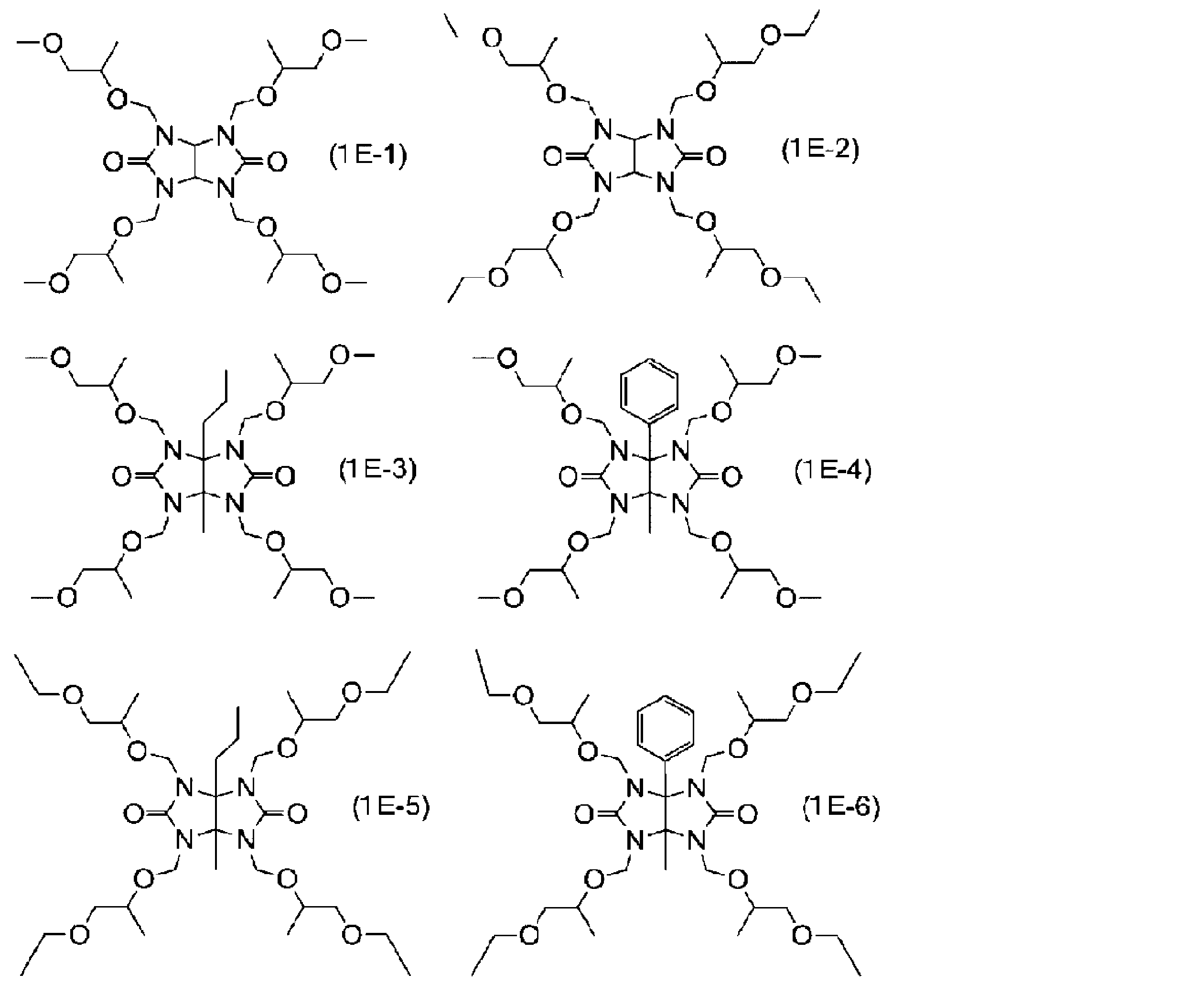
前記式(1d)で表される置換基を1分子中に2~6つ有する含窒素化合物は、窒素原子と結合する下記式(2d)で表される置換基を1分子中に2~6つ有する含窒素化合物と下記式(3d)で表される少なくとも1種の化合物とを反応させることで得られる。
The nitrogen-containing compound having 2 to 6 substituents represented by the formula (1d) in one molecule has 2 to 6 substituents in the molecule represented by the following formula (2d) bonded to the nitrogen atom. It can be obtained by reacting a nitrogen-containing compound with at least one compound represented by the following formula (3d).

(式(2d)及び式(3d)中、R1はメチル基又はエチル基を表し、R4は炭素原子数1~4のアルキル基を表す。)
(In formulas (2d) and (3d), R 1 represents a methyl group or an ethyl group, and R 4 represents an alkyl group having 1 to 4 carbon atoms.)
前記式(1E)で表されるグリコールウリル誘導体は、下記式(2E)で表されるグリコールウリル誘導体と前記式(3d)で表される少なくとも1種の化合物とを反応させることにより得られる。
The glycoluril derivative represented by the formula (1E) is obtained by reacting a glycoluril derivative represented by the following formula (2E) with at least one compound represented by the formula (3d).
前記式(2d)で表される置換基を1分子中に2~6つ有する含窒素化合物は、例えば、下記式(2E)で表されるグリコールウリル誘導体である。
A nitrogen-containing compound having 2 to 6 substituents represented by the above formula (2d) in one molecule is, for example, a glycoluril derivative represented by the following formula (2E).
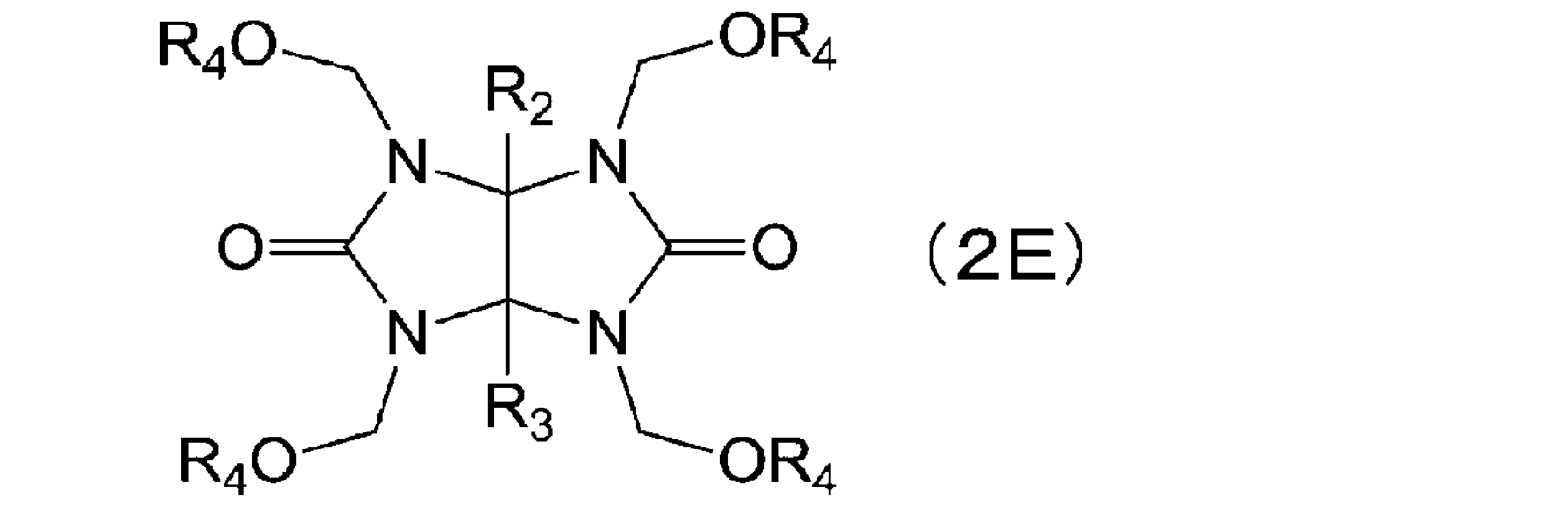
(式(2E)中、R2及びR3はそれぞれ独立に水素原子、炭素原子数1~4のアルキル基、又はフェニル基を表し、R4はそれぞれ独立に炭素原子数1~4のアルキル基を表す。)
(In formula (2E), R 2 and R 3 each independently represent a hydrogen atom, an alkyl group having 1 to 4 carbon atoms, or a phenyl group, and R 4 each independently represent an alkyl group having 1 to 4 carbon atoms. represents.)
前記式(2E)で表されるグリコールウリル誘導体として、例えば、下記式(2E-1)~式(2E-4)で表される化合物が挙げられる。さらに前記式(3d)で表される化合物として、例えば下記式(3d-1)及び式(3d-2)で表される化合物が挙げられる。
Examples of the glycoluril derivative represented by the formula (2E) include compounds represented by the following formulas (2E-1) to (2E-4). Furthermore, examples of the compound represented by the formula (3d) include compounds represented by the following formulas (3d-1) and (3d-2).


上記窒素原子と結合する下記式(1d)で表される置換基を1分子中に2~6つ有する含窒素化合物に係る内容については、WO2017/187969号公報の全開示が本願に援用される。
With respect to the content of the nitrogen-containing compound having 2 to 6 substituents represented by the following formula (1d) in one molecule that binds to the nitrogen atom, the full disclosure of WO2017/187969 is incorporated herein by reference. .
これらの架橋性化合物は単独で用いることも、2種類以上組み合わせて用いることもできる。架橋剤が使用される場合、その含有割合は、前記反応生成物に対し、通常1質量%~50質量%であり、好ましくは5質量%~30質量%である。また、その含有量は、環芳香族炭化水素基を含有するポリマー及び/又は化合物100重量部に対して1~200重量部であることが好ましい。
These crosslinkable compounds can be used alone or in combination of two or more. When a cross-linking agent is used, its content is generally 1% to 50% by mass, preferably 5% to 30% by mass, based on the reaction product. Also, the content thereof is preferably 1 to 200 parts by weight with respect to 100 parts by weight of the polymer and/or compound containing a ring aromatic hydrocarbon group.
本発明に係る光硬化性樹脂組成物は、WO2018/190380に記載の、下記式(1-1)乃至式(1-7)で表される部分構造(I)から選ばれる少なくとも一つの部分構造を含む化合物を更に含むことができる。:
The photocurable resin composition according to the present invention has at least one partial structure selected from partial structures (I) represented by the following formulas (1-1) to (1-7) described in WO2018/190380 can further include a compound comprising :

(式中、R1、R1a、R3、R5a、及びR6aはそれぞれ独立して炭素原子数1~10のアルキレン基、炭素原子数6~40のアリーレン基(該アルキレン基及びアリーレン基は、1つ又は2つ以上のアミド基又はアミノ基で任意に置換されていても良い)、酸素原子、カルボニル基、イオウ原子、-C(O)-NRa-、-NRb-又はそれらの組み合わせからなる2価の基を表し、
R5は、それぞれ独立して、窒素原子、又は窒素原子と炭素原子数1~10のアルキレン基、炭素原子数6~40のアリーレン基(該アルキレン基及びアリーレン基は、1つ又は2つ以上のアミド基又はアミノ基で任意に置換されていても良い)、酸素原子、カルボニル基、イオウ原子、-C(O)-NRa-及び-NRb-からなる群から選択される少なくとも一つ以上の基との組み合わせからなる3価の基を表し、
R2、R2a、R4、及びR6は、それぞれ独立して水素原子、炭素原子数1~10のアルキル基、又は水素原子と、炭素原子数1~10のアルキレン基、酸素原子、カルボニル基、-C(O)-NRa-及び-NRb-からなる群から選択される少なくとも一つ以上の基との組み合わせからなる1価の基を表し、
Raは水素原子又は炭素原子数1~10のアルキル基を表し、
Rbは、水素原子、炭素原子数1~10のアルキル基又は炭素原子数1~10のアルキルカルボニル基を表し、
nは1~10の繰り返し単位数を表し、及び
点線は隣接原子との化学結合を表す。) (wherein R 1 , R 1a , R 3 , R 5a and R 6a are each independently an alkylene group having 1 to 10 carbon atoms, an arylene group having 6 to 40 carbon atoms (the alkylene group and the arylene group optionally substituted with one or more amido or amino groups), an oxygen atom, a carbonyl group, a sulfur atom, —C(O)—NR a —, —NR b —, or Represents a divalent group consisting of a combination of
Each R 5 is independently a nitrogen atom, or a nitrogen atom and an alkylene group having 1 to 10 carbon atoms, or an arylene group having 6 to 40 carbon atoms (the alkylene group and arylene group are one or more at least one selected from the group consisting of an oxygen atom, a carbonyl group, a sulfur atom, —C(O)—NR a — and —NR b — Represents a trivalent group consisting of a combination of the above groups,
R 2 , R 2a , R 4 , and R 6 each independently represent a hydrogen atom, an alkyl group having 1 to 10 carbon atoms, or a hydrogen atom, an alkylene group having 1 to 10 carbon atoms, an oxygen atom, or a carbonyl represents a monovalent group in combination with at least one group selected from the group consisting of -C(O)-NR a - and -NR b -,
R a represents a hydrogen atom or an alkyl group having 1 to 10 carbon atoms,
R b represents a hydrogen atom, an alkyl group having 1 to 10 carbon atoms or an alkylcarbonyl group having 1 to 10 carbon atoms,
n represents the number of repeating units from 1 to 10, and dotted lines represent chemical bonds with adjacent atoms. )
WO2018/190380号公報の全開示が本願に参酌として援用される。
The entire disclosure of WO2018/190380 is incorporated herein by reference.
本発明に係る光硬化性樹脂組成物は、ポリシロキサンを更に含有してもよい。ポリシロキサンは、シラノール基の一部が変性されている変性ポリシロキサン、例えばシラノール基の一部がアルコール変性された又はアセタール保護されたポリシロキサン変性物であってもよい。
またポリシロキサンは、一例として加水分解性シランの加水分解縮合物であってもよいし、加水分解縮合物が有するシラノール基の少なくとも一部がアルコール変性された又はアセタール保護された変性物(以下、「加水分解縮合物の変性物」と称することがある。)であってもよい。加水分解縮合物に係る加水分解性シランは、一種又は二種以上の加水分解性シランを含むことができる。
ポリシロキサンは、かご型、ラダー型、直鎖型、及び分岐型のいずれの主鎖を有する構造であるものとすることができる。さらに市販のポリシロキサンを使用することができる。 The photocurable resin composition according to the present invention may further contain polysiloxane. The polysiloxane may be a modified polysiloxane in which some of the silanol groups are modified, for example, a modified polysiloxane in which some of the silanol groups are alcohol-modified or acetal-protected.
Polysiloxane may be, for example, a hydrolytic condensate of a hydrolyzable silane, or a modified product in which at least part of the silanol groups of the hydrolytic condensate is alcohol-modified or acetal-protected (hereinafter referred to as It may be referred to as a “modified product of hydrolytic condensate”.). The hydrolyzable silane associated with the hydrolytic condensate can contain one or more hydrolyzable silanes.
The polysiloxane can have any structure having a cage-type, ladder-type, straight-chain, or branched main chain. Furthermore, commercially available polysiloxanes can be used.
なお、本発明において、加水分解性シランの「加水分解縮合物」、すなわち加水分解縮合の生成物には、縮合が完全に完了した縮合物であるポリオルガノシロキサンポリマーだけでなく、縮合が完全に完了しない部分加水分解縮合物であるポリオルガノシロキサンポリマーも包含される。このような部分加水分解縮合物も、縮合が完全に完了した縮合物と同様、加水分解性シランの加水分解及び縮合によって得られたポリマーであるが、部分的に加水分解で止まり、縮合しておらず、それ故、Si-OH基が残存しているものである。
In the present invention, the "hydrolytic condensate" of the hydrolyzable silane, that is, the product of hydrolytic condensation, includes not only the polyorganosiloxane polymer, which is a condensate in which the condensation has been completely completed, but also Also included are polyorganosiloxane polymers that are incomplete partial hydrolytic condensates. Such a partially hydrolyzed condensate is also a polymer obtained by hydrolysis and condensation of a hydrolyzable silane, similar to the condensate in which the condensation is completely completed, but it stops at partial hydrolysis and condenses. , and therefore the Si--OH groups remain.
かかるポリシロキサンとして、例えば下記式(11)で表される少なくとも1種の加水分解性シランを含む加水分解性シランの加水分解縮合物又はその変性物を挙げることができる。
Examples of such polysiloxanes include hydrolytic condensates of hydrolyzable silanes containing at least one hydrolyzable silane represented by the following formula (11) or modified products thereof.

式(11)中、R1は、ケイ素原子に結合する基であって、互いに独立して、置換されていてもよいアルキル基、置換されていてもよいアリール基、置換されていてもよいアラルキル基、置換されていてもよいハロゲン化アルキル基、置換されていてもよいハロゲン化アリール基、置換されていてもよいハロゲン化アラルキル基、置換されていてもよいアルコキシアルキル基、置換されていてもよいアルコキシアリール基、置換されていてもよいアルコキシアラルキル基、若しくは置換されていてもよいアルケニル基を表すか、又はエポキシ基を有する有機基、アクリロイル基を有する有機基、メタクリロイル基を有する有機基、メルカプト基を有する有機基、アミノ基を有する有機基、アルコキシ基を有する有機基、スルホニル基を有する有機基、若しくはシアノ基を有する有機基、又はそれらの2種以上の組み合わせを表す。
またR2は、ケイ素原子に結合する基又は原子であって、互いに独立して、アルコキシ基、アラルキルオキシ基、アシルオキシ基、又はハロゲン原子を表す。
aは0~3の整数を表す。 In formula (11), R 1 is a group bonded to a silicon atom and independently of each other, an optionally substituted alkyl group, an optionally substituted aryl group, an optionally substituted aralkyl optionally substituted halogenated alkyl group, optionally substituted halogenated aryl group, optionally substituted halogenated aralkyl group, optionally substituted alkoxyalkyl group, optionally substituted an alkoxyaryl group, an optionally substituted alkoxyaralkyl group, or an optionally substituted alkenyl group, or an organic group having an epoxy group, an organic group having an acryloyl group, or an organic group having a methacryloyl group; It represents an organic group having a mercapto group, an organic group having an amino group, an organic group having an alkoxy group, an organic group having a sulfonyl group, an organic group having a cyano group, or a combination of two or more thereof.
R 2 is a group or atom bonded to a silicon atom and independently represents an alkoxy group, an aralkyloxy group, an acyloxy group, or a halogen atom.
a represents an integer of 0 to 3;
式(11)中のR1における各基及び原子の具体例、並びにそれらの好適な炭素数としては、式(A-1)及び(A-2)中のR3について前述した基及び炭素数を挙げることができる。
式(11)中のR2における各基及び原子の具体例、並びにそれらの好適な炭素数としては、式(A-1)及び(A-2)中のXについて前述した基及び原子並びに炭素数を挙げることができる。 Specific examples of each group and atom in R 1 in formula (11) and preferred carbon numbers thereof include the groups and carbon numbers described above for R 3 in formulas (A-1) and (A-2). can be mentioned.
Specific examples of each group and atom for R 2 in formula (11) and their preferred number of carbon atoms include the groups and atoms described above for X in formulas (A-1) and (A-2), and carbon I can name a few.
式(11)で表される加水分解性シランの具体例としては、テトラメトキシシラン、テトラクロロシラン、テトラアセトキシシラン、テトラエトキシシラン、テトラ-n-プロポキシシラン、テトラ-i-プロポキシシラン、テトラ-n-ブトキシシラン、メチルトリメトキシシラン、メチルトリクロロシラン、メチルトリアセトキシシラン、メチルトリエトキシシラン、メチルトリプロポキシシラン、メチルトリブトキシシラン、メチルトリアミロキシシラン、メチルトリフェノキシシラン、メチルトリベンジルオキシシラン、メチルトリフェネチルオキシシラン、グリシドキシメチルトリメトキシシラン、グリシドキシメチルトリエトキシシラン、α-グリシドキシエチルトリメトキシシラン、α-グリシドキシエチルトリエトキシシラン、β-グリシドキシエチルトリメトキシシラン、β-グリシドキシエチルトリエトキシシラン、α-グリシドキシプロピルトリメトキシシラン、α-グリシドキシプロピルトリエトキシシラン、β-グリシドキシプロピルトリメトキシシラン、β-グリシドキシプロピルトリエトキシシラン、γ-グリシドキシプロピルトリメトキシシラン、γ-グリシドキシプロピルトリエトキシシラン、γ-グリシドキシプロピルトリプロポキシシラン、γ-グリシドキシプロピルトリブトキシシラン、γ-グリシドキシプロピルトリフェノキシシラン、α-グリシドキシブチルトリメトキシシラン、α-グリシドキシブチルトリエトキシシラン、β-グリシドキシブチルトリエトキシシラン、γ-グリシドキシブチルトリメトキシシラン、γ-グリシドキシブチルトリエトキシシラン、δ-グリシドキシブチルトリメトキシシラン、δ-グリシドキシブチルトリエトキシシラン、(3,4-エポキシシクロヘキシル)メチルトリメトキシシラン、(3,4-エポキシシクロヘキシル)メチルトリエトキシシラン、β-(3,4-エポキシシクロヘキシル)エチルトリメトキシシラン、β-(3,4-エポキシシクロヘキシル)エチルトリエトキシシラン、β-(3,4-エポキシシクロヘキシル)エチルトリプロポキシシラン、β-(3,4-エポキシシクロヘキシル)エチルトリブトキシシラン、β-(3,4-エポキシシクロヘキシル)エチルトリフェノキシシラン、γ-(3,4-エポキシシクロヘキシル)プロピルトリメトキシシラン、γ-(3,4-エポキシシクロヘキシル)プロピルトリエトキシシラン、δ-(3,4-エポキシシクロヘキシル)ブチルトリメトキシシラン、δ-(3,4-エポキシシクロヘキシル)ブチルトリエトキシシラン、グリシドキシメチルメチルジメトキシシラン、グリシドキシメチルメチルジエトキシシラン、α-グリシドキシエチルメチルジメトキシシラン、α-グリシドキシエチルメチルジエトキシシラン、β-グリシドキシエチルメチルジメトキシシラン、β-グリシドキシエチルエチルジメトキシシラン、α-グリシドキシプロピルメチルジメトキシシラン、α-グリシドキシプロピルメチルジエトキシシラン、β-グリシドキシプロピルメチルジメトキシシラン、β-グリシドキシプロピルエチルジメトキシシラン、γ-グリシドキシプロピルメチルジメトキシシラン、γ-グリシドキシプロピルメチルジエトキシシラン、γ-グリシドキシプロピルメチルジプロポキシシラン、γ-グリシドキシプロピルメチルジブトキシシラン、γ-グリシドキシプロピルメチルジフェノキシシラン、γ-グリシドキシプロピルエチルジメトキシシラン、γ-グリシドキシプロピルエチルジエトキシシラン、γ-グリシドキシプロピルビニルジメトキシシラン、γ-グリシドキシプロピルビニルジエトキシシラン、エチルトリメトキシシラン、エチルトリエトキシシラン、ビニルトリメトキシシラン、ビニルトリエトキシシラン、ビニルトリクロロシラン、ビニルトリアセトキシシラン、メチルビニルジメトキシシラン、メチルビニルジエトキシシラン、メチルビニルジクロロシラン、メチルビニルジアセトキシシラン、ジメチルビニルメトキシシラン、ジメチルビニルエトキシシラン、ジメチルビニルクロロシラン、ジメチルビニルアセトキシシラン、ジビニルジメトキシシラン、ジビニルジエトキシシラン、ジビニルジクロロシラン、ジビニルジアセトキシシラン、γ-グリシドキシプロピルビニルジメトキシシラン、γ-グリシドキシプロピルビニルジエトキシシラン、アリルトリメトキシシラン、アリルトリエトキシシラン、アリルトリクロロシラン、アリルトリアセトキシシシラン、アリルメチルジメトキシシラン、アリルメチルジエトキシシラン、アリルメチルジクロロシラン、アリルメチルジアセトキシシラン、アリルジメチルメトキシシラン、アリルジメチルエトキシシラン、アリルジメチルクロロシラン、アリルジメチルアセトキシシラン、ジアリルジメトキシシラン、ジアリルジエトキシシラン、ジアリルジクロロシラン、ジアリルジアセトキシシラン、3-アリルアミノプロピルトリメトキシシラン、3-アリルアミノプロピルトリエトキシシラン、p-スチリルトリメトキシシラン、フェニルトリメトキシシラン、フェニルトリエトキシシラン、フェニルトリクロロシラン、フェニルトリアセトキシシラン、フェニルメチルジメトキシシラン、フェニルメチルジエトキシシラン、フェニルメチルジクロロシラン、フェニルメチルジアセトキシシラン、フェニルジメチルメトキシシラン、フェニルジメチルエトキシシラン、フェニルジメチルクロロシラン、フェニルジメチルアセトキシシラン、ジフェニルメチルメトキシシラン、ジフェニルメチルエトキシシラン、ジフェニルメチルクロロシラン、ジフェニルメチルアセトキシシラン、ジフェニルジメトキシシラン、ジフェニルジエトキシシラン、ジフェニルジクロロシラン、ジフェニルジアセトキシシラン、トリフェニルメトキシシシラン、トリフェニルエトキシシラン、トリフェニルアセトキシシラン、トリフェニルクロロシラン、3-フェニルアミノプロピルトリメトキシシラン、3-フェニルアミノプロピルトリエトキシシラン、ジメトキシメチル-3-(3-フェノキシプロピルチオプロピル)シラン、トリエトキシ((2-メトキシ-4-(メトキシメチル)フェノキシ)メチル)シラン、ベンジルトリメトキシシラン、ベンジルトリエトキシシラン、ベンジルメチルジメトキシシラン、ベンジルメチルジエトキシシラン、ベンジルジメチルメトキシシラン、ベンジルジメチルエトキシシラン、ベンジルジメチルクロロシラン、フェネチルトリメトキシシラン、フェネチルトリエトキシシラン、フェネチルトリクロロシラン、フェネチルトリアセトキシシラン、フェネチルメチルジメトキシシラン、フェネチルメチルジエトキシシラン、フェネチルメチルジクロロシラン、フェネチルメチルジアセトキシシラン、メトキシフェニルトリメトキシシラン、メトキシフェニルトリエトキシシラン、メトキシフェニルトリアセトキシシラン、メトキシフェニルトリクロロシラン、メトキシベンジルトリメトキシシラン、メトキシベンジルトリエトキシシラン、メトキシベンジルトリアセトキシシラン、メトキシベンジルトリクロロシラン、メトキシフェネチルトリメトキシシラン、メトキシフェネチルトリエトキシシラン、メトキシフェネチルトリアセトキシシラン、メトキシフェネチルトリクロロシラン、エトキシフェニルトリメトキシシラン、エトキシフェニルトリエトキシシラン、エトキシフェニルトリアセトキシシラン、エトキシフェニルトリクロロシラン、エトキシベンジルトリメトキシシラン、エトキシベンジルトリエトキシシラン、エトキシベンジルトリアセトキシシラン、エトキシベンジルトリクロロシラン、i-プロポキシフェニルトリメトキシシラン、i-プロポキシフェニルトリエトキシシラン、i-プロポキシフェニルトリアセトキシシラン、i-プロポキシフェニルトリクロロシラン、i-プロポキシベンジルトリメトキシシラン、i-プロポキシベンジルトリエトキシシラン、i-プロポキシベンジルトリアセトキシシラン、i-プロポキシベンジルトリクロロシラン、t-ブトキシフェニルトリメトキシシラン、t-ブトキシフェニルトリエトキシシラン、t-ブトキシフェニルトリアセトキシシラン、t-ブトキシフェニルトリクロロシラン、t-ブトキシベンジルトリメトキシシラン、t-ブトキシベンジルトリエトキシシラン、t-ブトキシベンジルトリアセトキシシラン、t-ブトキシシベンジルトリクロロシラン、メトキシナフチルトリメトキシシラン、メトキシナフチルトリエトキシシラン、メトキシナフチルトリアセトキシシラン、メトキシナフチルトリクロロシラン、エトキシナフチルトリメトキシシラン、エトキシナフチルトリエトキシシラン、エトキシナフチルトリアセトキシシラン、エトキシナフチルトリクロロシラン、γ-クロロプロピルトリメトキシシラン、γ-クロロプロピルトリエトキシシラン、γ-クロロプロピルトリアセトキシシラン、3,3,3-トリフルオロプロピルトリメトキシシラン、γ-メタクリルオキシプロピルトリメトキシシラン、γ-メルカプトプロピルトリメトキシシラン、γ-メルカプトプロピルトリエトキシシラン、β-シアノエチルトリエトキシシラン、チオシアネートプロピルトリエトキシシラン、クロロメチルトリメトキシシラン、クロロメチルトリエトキシシラン、トリエトキシシリルプロピルジアリルイソシアヌレート、ビシクロ[2,2,1]ヘプテニルトリエトキシシラン、ベンゼンスルホニルプロピルトリエトキシシラン、ベンゼンスルホンアミドプロピルトリエトキシシラン、ジメチルアミノプロピルトリメトキシシラン、ジメチルジメトキシシラン、フェニルメチルジメトキシシラン、ジメチルジエトキシシラン、フェニルメチルジエトキシシラン、γ-クロロプロピルメチルジメトキシシラン、γ-クロロプロピルメチルジエトキシシラン、ジメチルジアセトキシシラン、γ-メタクリルオキシプロピルメチルジメトキシシラン、γ-メタクリルオキシプロピルメチルジエトキシシラン、γ-メルカプトプロピルメチルジメトキシシラン、γ-メルカプトメチルジエトキシシラン、メチルビニルジメトキシシラン、メチルビニルジエトキシシランが挙げられるが、これらに限定されない。
Specific examples of hydrolyzable silanes represented by formula (11) include tetramethoxysilane, tetrachlorosilane, tetraacetoxysilane, tetraethoxysilane, tetra-n-propoxysilane, tetra-i-propoxysilane, tetra-n -butoxysilane, methyltrimethoxysilane, methyltrichlorosilane, methyltriacetoxysilane, methyltriethoxysilane, methyltripropoxysilane, methyltributoxysilane, methyltriamyloxysilane, methyltriphenoxysilane, methyltribenzyloxysilane, methyltriphenethyloxysilane, glycidoxymethyltrimethoxysilane, glycidoxymethyltriethoxysilane, α-glycidoxyethyltrimethoxysilane, α-glycidoxyethyltriethoxysilane, β-glycidoxyethyltrimethoxysilane Silane, β-glycidoxyethyltriethoxysilane, α-glycidoxypropyltrimethoxysilane, α-glycidoxypropyltriethoxysilane, β-glycidoxypropyltrimethoxysilane, β-glycidoxypropyltriethoxy Silane, γ-glycidoxypropyltrimethoxysilane, γ-glycidoxypropyltriethoxysilane, γ-glycidoxypropyltripropoxysilane, γ-glycidoxypropyltributoxysilane, γ-glycidoxypropyltriphenoxy Silane, α-glycidoxybutyltrimethoxysilane, α-glycidoxybutyltriethoxysilane, β-glycidoxybutyltriethoxysilane, γ-glycidoxybutyltrimethoxysilane, γ-glycidoxybutyltriethoxysilane Silane, δ-glycidoxybutyltrimethoxysilane, δ-glycidoxybutyltriethoxysilane, (3,4-epoxycyclohexyl)methyltrimethoxysilane, (3,4-epoxycyclohexyl)methyltriethoxysilane, β- (3,4-epoxycyclohexyl)ethyltrimethoxysilane, β-(3,4-epoxycyclohexyl)ethyltriethoxysilane, β-(3,4-epoxycyclohexyl)ethyltripropoxysilane, β-(3,4- epoxycyclohexyl)ethyltributoxysilane, β-(3,4-epoxycyclohexyl)ethyltriphenoxysilane, γ-(3,4-epoxycyclohexyl)propyltrimethoxysilane, γ-(3,4-epoxycyclohexyl)propyltri ethoxysilane, δ-(3,4-epoxycyclohexyl)butyltrimethoxysilane, δ-(3,4-epoxycyclohexyl)butyltriethoxysilane, glycidoxymethylmethyldimethoxysilane, glycidoxymethylmethyldiethoxysilane, α-Glycidoxyethylmethyldimethoxysilane, α-glycidoxyethylmethyldiethoxysilane, β-glycidoxyethylmethyldimethoxysilane, β-glycidoxyethylethyldimethoxysilane, α-glycidoxypropylmethyldimethoxysilane , α-glycidoxypropylmethyldiethoxysilane, β-glycidoxypropylmethyldimethoxysilane, β-glycidoxypropylethyldimethoxysilane, γ-glycidoxypropylmethyldimethoxysilane, γ-glycidoxypropylmethyldimethoxysilane, γ-glycidoxypropylmethyldimethoxysilane, Ethoxysilane, γ-glycidoxypropylmethyldipropoxysilane, γ-glycidoxypropylmethyldibutoxysilane, γ-glycidoxypropylmethyldiphenoxysilane, γ-glycidoxypropylethyldimethoxysilane, γ-glycid Xypropylethyldiethoxysilane, γ-glycidoxypropylvinyldimethoxysilane, γ-glycidoxypropylvinyldiethoxysilane, ethyltrimethoxysilane, ethyltriethoxysilane, vinyltrimethoxysilane, vinyltriethoxysilane, vinyltri Chlorosilane, vinyltriacetoxysilane, methylvinyldimethoxysilane, methylvinyldiethoxysilane, methylvinyldichlorosilane, methylvinyldiacetoxysilane, dimethylvinylmethoxysilane, dimethylvinylethoxysilane, dimethylvinylchlorosilane, dimethylvinylacetoxysilane, divinyldimethoxysilane Silane, divinyldiethoxysilane, divinyldichlorosilane, divinyldiacetoxysilane, γ-glycidoxypropylvinyldimethoxysilane, γ-glycidoxypropylvinyldiethoxysilane, allyltrimethoxysilane, allyltriethoxysilane, allyltrichlorosilane , allyltriacetoxysilane, allylmethyldimethoxysilane, allylmethyldiethoxysilane, allylmethyldichlorosilane, allylmethyldiacetoxysilane, allyldimethylmethoxysilane, allyldimethylethoxysilane, allyldimethylchlorosilane, allyldimethylacetoxysilane, diallyldimethoxysilane Silane, diallyldiethoxysilane, diallyldichlorosilane, diallyldiacetoxysilane, 3-allylaminopropyltrimethoxysilane, 3-allylaminopropyltriethoxysilane, p-styryltrimethoxysilane, phenyltrimethoxysilane, phenyltriethoxysilane , phenyltrichlorosilane, phenyltriacetoxysilane, phenylmethyldimethoxysilane, phenylmethyldiethoxysilane, phenylmethyldichlorosilane, phenylmethyldiacetoxysilane, phenyldimethylmethoxysilane, phenyldimethylethoxysilane, phenyldimethylchlorosilane, phenyldimethylacetoxysilane , diphenylmethylmethoxysilane, diphenylmethylethoxysilane, diphenylmethylchlorosilane, diphenylmethylacetoxysilane, diphenyldimethoxysilane, diphenyldiethoxysilane, diphenyldichlorosilane, diphenyldiacetoxysilane, triphenylmethoxysilane, triphenylethoxysilane, tri phenylacetoxysilane, triphenylchlorosilane, 3-phenylaminopropyltrimethoxysilane, 3-phenylaminopropyltriethoxysilane, dimethoxymethyl-3-(3-phenoxypropylthiopropyl)silane, triethoxy ((2-methoxy-4- (methoxymethyl)phenoxy)methyl)silane, benzyltrimethoxysilane, benzyltriethoxysilane, benzylmethyldimethoxysilane, benzylmethyldiethoxysilane, benzyldimethylmethoxysilane, benzyldimethylethoxysilane, benzyldimethylchlorosilane, phenethyltrimethoxysilane, phenethyltriethoxysilane, phenethyltrichlorosilane, phenethyltriacetoxysilane, phenethylmethyldimethoxysilane, phenethylmethyldiethoxysilane, phenethylmethyldichlorosilane, phenethylmethyldiacetoxysilane, methoxyphenyltrimethoxysilane, methoxyphenyltriethoxysilane, methoxyphenyl triacetoxysilane, methoxyphenyltrichlorosilane, methoxybenzyltrimethoxysilane, methoxybenzyltriethoxysilane, methoxybenzyltriacetoxysilane, methoxybenzyltrichlorosilane, methoxyphenethyltrimethoxysilane, methoxyphenethyltriethoxysilane, methoxyphenethyltriacetoxysilane, Methoxyphenethyltrichlorosilane, ethoxyphenyltrimethoxysilane, ethoxyphenyltriethoxysilane, ethoxyphenyltriacetoxysilane, ethoxyphenyltrichlorosilane, ethoxybenzyltrimethoxysilane, ethoxybenzyltriethoxysilane, ethoxybenzyltriacetoxysilane, ethoxybenzyltrichlorosilane , i-propoxyphenyltrimethoxysilane, i-propoxyphenyltriethoxysilane, i-propoxyphenyltriacetoxysilane, i-propoxyphenyltrichlorosilane, i-propoxybenzyltrimethoxysilane, i-propoxybenzyltriethoxysilane, i- Propoxybenzyltriacetoxysilane, i-propoxybenzyltrichlorosilane, t-butoxyphenyltrimethoxysilane, t-butoxyphenyltriethoxysilane, t-butoxyphenyltriacetoxysilane, t-butoxyphenyltrichlorosilane, t-butoxybenzyltrimethoxysilane Silane, t-butoxybenzyltriethoxysilane, t-butoxybenzyltriacetoxysilane, t-butoxybenzyltrichlorosilane, methoxynaphthyltrimethoxysilane, methoxynaphthyltriethoxysilane, methoxynaphthyltriacetoxysilane, methoxynaphthyltrichlorosilane, ethoxy naphthyltrimethoxysilane, ethoxynaphthyltriethoxysilane, ethoxynaphthyltriacetoxysilane, ethoxynaphthyltrichlorosilane, γ-chloropropyltrimethoxysilane, γ-chloropropyltriethoxysilane, γ-chloropropyltriacetoxysilane, 3,3, 3-trifluoropropyltrimethoxysilane, γ-methacryloxypropyltrimethoxysilane, γ-mercaptopropyltrimethoxysilane, γ-mercaptopropyltriethoxysilane, β-cyanoethyltriethoxysilane, thiocyanatepropyltriethoxysilane, chloromethyltriethoxysilane Methoxysilane, chloromethyltriethoxysilane, triethoxysilylpropyl diallyl isocyanurate, bicyclo[2,2,1]heptenyltriethoxysilane, benzenesulfonylpropyltriethoxysilane, benzenesulfonamidopropyltriethoxysilane, dimethylaminopropyltriethoxysilane Methoxysilane, dimethyldimethoxysilane, phenylmethyldimethoxysilane, dimethyldiethoxysilane, phenylmethyldiethoxysilane, γ-chloropropylmethyldimethoxysilane, γ-chloropropylmethyldiethoxysilane, dimethyldiacetoxysilane, γ-methacryloxypropyl Examples include, but are not limited to, methyldimethoxysilane, γ-methacryloxypropylmethyldiethoxysilane, γ-mercaptopropylmethyldimethoxysilane, γ-mercaptomethyldiethoxysilane, methylvinyldimethoxysilane, methylvinyldiethoxysilane.
本発明に係る光硬化性樹脂組成物は、特開2016-003160号公報に記載の、
(A)多官能エポキシ(メタ)アクリレート化合物、
(B)多官能チオール化合物、及び
(C)ラジカル重合開始剤を更に含有するものであってよい。 The photocurable resin composition according to the present invention is described in JP-A-2016-003160,
(A) a polyfunctional epoxy (meth)acrylate compound,
(B) a polyfunctional thiol compound and (C) a radical polymerization initiator may be further contained.
上記(A)成分の分子量が300~20,000であってよい。
上記(A)成分がビスフェノール型多官能エポキシ(メタ)アクリレート化合物であってよい。
上記(B)成分が25℃で液状であってよい。
更に、(D)重合禁止剤を含有してよい。 The component (A) may have a molecular weight of 300 to 20,000.
The component (A) may be a bisphenol-type polyfunctional epoxy (meth)acrylate compound.
The component (B) may be liquid at 25°C.
Furthermore, (D) a polymerization inhibitor may be contained.
特開2016-003160号公報の全開示が本願に参酌として援用される。
The full disclosure of Japanese Patent Application Laid-Open No. 2016-003160 is incorporated into the present application as a reference.
本発明に係る光硬化性樹脂組成物は、WO2009/104643に記載の、光重合性物質及び光重合開始剤を更に含む膜形成組成物であってよい。
前記光重合性物質がカチオン重合可能な反応性基を少なくとも一つ有する化合物であり、前記カチオン重合開始剤が光カチオン重合開始剤であってよい。
前記光重合性物質がラジカル重合可能な反応性基を少なくとも一つ有する化合物であり、前記光重合開始剤が光ラジカル重合開始剤であってよい。 The photocurable resin composition according to the present invention may be a film-forming composition further comprising a photopolymerizable substance and a photoinitiator, as described in WO2009/104643.
The photopolymerizable substance may be a compound having at least one cationic polymerizable reactive group, and the cationic polymerization initiator may be a photocationic polymerization initiator.
The photopolymerizable substance may be a compound having at least one radically polymerizable reactive group, and the photopolymerization initiator may be a radical photopolymerization initiator.
前記光重合性化合物が糖化合物であってよい。
前記糖化合物が単糖類又は二糖類化合物であってよい。
前記糖化合物が式(10): The photopolymerizable compound may be a sugar compound.
The sugar compounds may be monosaccharide or disaccharide compounds.
The sugar compound has the formula (10):
前記糖化合物が単糖類又は二糖類化合物であってよい。
前記糖化合物が式(10): The photopolymerizable compound may be a sugar compound.
The sugar compounds may be monosaccharide or disaccharide compounds.
The sugar compound has the formula (10):

(ただし、G1は糖骨格を示し、Tは2価の連結基を示し、R1はビニル基又はグリシジル基を示し、R2は水素原子又は水酸基を示す。n及びLはそれぞれ0又は1の整数を示し、pは整数であって糖が有する水酸基の総数である。mは1≦m≦(p-m)を満たす整数である。)であってよい。
(where G 1 represents a sugar skeleton, T represents a divalent linking group, R 1 represents a vinyl group or glycidyl group, R 2 represents a hydrogen atom or a hydroxyl group, n and L are 0 or 1, respectively. p is an integer representing the total number of hydroxyl groups possessed by the sugar, and m is an integer satisfying 1≦m≦(pm).
前記光重合性化合物が脂環式エポキシ化合物、又は脂環式オキセタン化合物であってよい。
前記脂環式エポキシ化合物がシクロアルキレンオキシド誘導体であってよい。
前記脂環式エポキシ化合物が式(2)又は式(3): The photopolymerizable compound may be an alicyclic epoxy compound or an alicyclic oxetane compound.
The alicyclic epoxy compound may be a cycloalkylene oxide derivative.
The alicyclic epoxy compound is represented by formula (2) or formula (3):
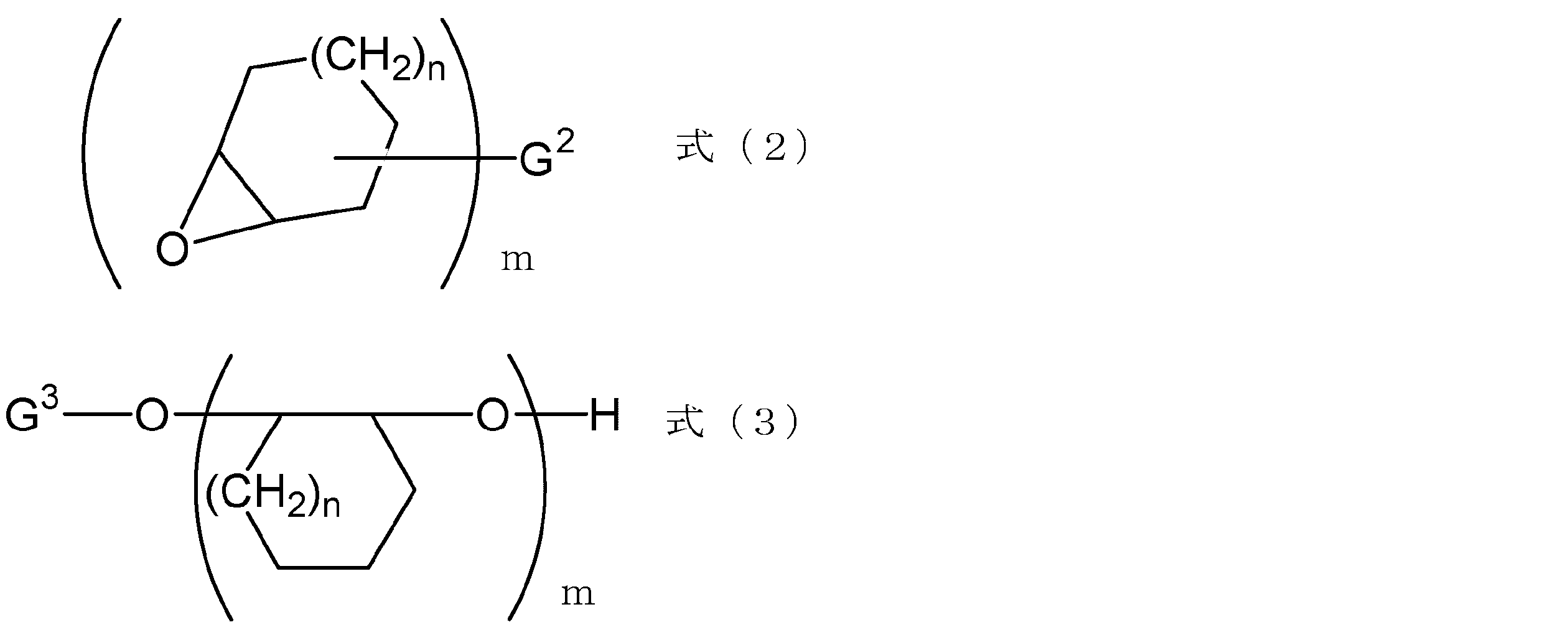
(ただし、G2はアルキレン基、カルボニルオキシ基、ヘテロ環、芳香環、又はこれらの組み合わせを有する1価~5価の連結基を示し、G3はアルキル基、アルキルカルボニル基、ヘテロ環、芳香環、又はこれらの組み合わせを有する有機基であり、n及びmはそれぞれ1~5の整数を示す。)であってよい。
(where G2 represents a monovalent to pentavalent linking group having an alkylene group, carbonyloxy group, heterocyclic ring, aromatic ring, or a combination thereof; G3 represents an alkyl group, an alkylcarbonyl group, a heterocyclic ring, an aromatic an organic group having a ring or a combination thereof, and n and m each represent an integer of 1 to 5).
WO2009/104643の全開示が本願に参酌として援用される。
The full disclosure of WO2009/104643 is incorporated herein by reference.
本願の光硬化性樹脂組成物の調製方法は、特に限定されない。すなわち、多環芳香族炭化水素基を含有するポリマー及び/又は化合物、溶剤、その他の成分を任意の割合で任意の順で混合し、均一な溶液とすればよい。こうして調製された溶液状態の光硬化性樹脂組成物は、孔径が0.2μm程度のフィルタ等を用いて濾過した後に使用することが好ましい。
The method for preparing the photocurable resin composition of the present application is not particularly limited. That is, a polymer and/or compound containing a polycyclic aromatic hydrocarbon group, a solvent, and other components may be mixed in an arbitrary ratio and in an arbitrary order to form a uniform solution. The photocurable resin composition in a solution state thus prepared is preferably used after being filtered using a filter or the like having a pore size of about 0.2 μm.
本発明に係る光硬化性樹脂組成物において、固形分、すなわち前記溶剤を除いた成分の濃度範囲は、用途により適宜選択することができる。例えば、レジスト下層膜形成のためには通常5~50質量%であり、好ましくは10~30質量%であり、半導体製造用ウエハ端部保護膜を形成するためには通常0.01質量%~10質量%である。
In the photocurable resin composition according to the present invention, the solid content, that is, the concentration range of the components excluding the solvent can be appropriately selected depending on the application. For example, it is usually 5 to 50% by mass, preferably 10 to 30% by mass, for forming a resist underlayer film, and usually 0.01% by mass to 0.01% by mass for forming a wafer edge protection film for semiconductor manufacturing. 10% by mass.
<半導体装置の製造方法>
本発明に係る光硬化性樹脂組成物を半導体基板上に塗布し、塗布された組成物を焼成することによりレジスト下層膜を製造し、これを利用して半導体装置を製造することができる。 <Method for manufacturing a semiconductor device>
The photocurable resin composition according to the present invention is coated on a semiconductor substrate, and the coated composition is baked to produce a resist underlayer film, which can be used to produce a semiconductor device.
本発明に係る光硬化性樹脂組成物が塗布される半導体基板としては、例えば、シリコンウエハ、ゲルマニウムウエハ、及びヒ化ガリウム、リン化インジウム、窒化ガリウム、窒化インジウム、窒化アルミニウム等の化合物半導体ウエハが挙げられる。
Semiconductor substrates to which the photocurable resin composition according to the present invention is applied include, for example, silicon wafers, germanium wafers, and compound semiconductor wafers such as gallium arsenide, indium phosphide, gallium nitride, indium nitride, and aluminum nitride. mentioned.
表面に無機膜が形成された半導体基板を用いる場合、当該無機膜は、例えば、ALD(原子層堆積)法、CVD(化学気相堆積)法、反応性スパッタ法、イオンプレーティング法、真空蒸着法、スピンコーティング法(スピンオングラス:SOG)により形成される。前記無機膜として、例えば、ポリシリコン膜、酸化ケイ素膜、窒化珪素膜、BPSG(Boro-Phospho Silicate Glass)膜、窒化チタン膜、窒化酸化チタン膜、タングステン膜、窒化ガリウム膜、及びヒ化ガリウム膜が挙げられる。
When using a semiconductor substrate having an inorganic film formed on its surface, the inorganic film is formed by, for example, an ALD (atomic layer deposition) method, a CVD (chemical vapor deposition) method, a reactive sputtering method, an ion plating method, or a vacuum deposition method. It is formed by a spin coating method (spin on glass: SOG). Examples of the inorganic film include a polysilicon film, a silicon oxide film, a silicon nitride film, a BPSG (Boro-Phospho Silicate Glass) film, a titanium nitride film, a titanium oxynitride film, a tungsten film, a gallium nitride film, and a gallium arsenide film. is mentioned.
このような半導体基板上に、スピナー、コーター等の適当な塗布方法により本発明に係る光硬化性樹脂組成物を塗布する。その後、ホットプレート等の加熱手段を用いてベークすることによりレジスト下層膜を形成する。ベーク条件としては、ベーク温度100℃~400℃、ベーク時間0.3分~60分間の中から適宜、選択される。好ましくは、ベーク温度120℃~350℃、ベーク時間0.5分~30分間、より好ましくは、ベーク温度150℃~300℃、ベーク時間0.8分~10分間である。
The photocurable resin composition according to the present invention is applied onto such a semiconductor substrate by an appropriate coating method such as spinner or coater. Thereafter, a resist underlayer film is formed by baking using a heating means such as a hot plate. Baking conditions are appropriately selected from a baking temperature of 100° C. to 400° C. and a baking time of 0.3 minutes to 60 minutes. Preferably, the baking temperature is 120° C. to 350° C. and the baking time is 0.5 minutes to 30 minutes, and more preferably the baking temperature is 150° C. to 300° C. and the baking time is 0.8 minutes to 10 minutes.
形成されるレジスト下層膜の膜厚としては、例えば0.001μm(1nm)~10μm、0.002μm(2nm)~1μm、0.005μm(5nm)~0.5μm(500nm)、0.001μm(1nm)~0.05μm(50nm)、0.002μm(2nm)~0.05μm(50nm)、0.003μm(1nm)~0.05μm(50nm)、0.004μm(4nm)~0.05μm(50nm)、0.005μm(5nm)~0.05μm(50nm)、0.003μm(3nm)~0.03μm(30nm)、0.003μm(3nm)~0.02μm(20nm)、0.005μm(5nm)~0.02μm(20nm)である。
The film thickness of the resist underlayer film to be formed is, for example, 0.001 μm (1 nm) to 10 μm, 0.002 μm (2 nm) to 1 μm, 0.005 μm (5 nm) to 0.5 μm (500 nm), 0.001 μm (1 nm). ) ~ 0.05 µm (50 nm), 0.002 µm (2 nm) ~ 0.05 µm (50 nm), 0.003 µm (1 nm) ~ 0.05 µm (50 nm), 0.004 µm (4 nm) ~ 0.05 µm (50 nm) , 0.005 μm (5 nm) to 0.05 μm (50 nm), 0.003 μm (3 nm) to 0.03 μm (30 nm), 0.003 μm (3 nm) to 0.02 μm (20 nm), 0.005 μm (5 nm) to 0.02 μm (20 nm).
パターンニングされた基板の製造方法は以下の工程を経る。通常、レジスト下層膜の上にフォトレジスト層を形成して製造される。レジスト下層膜の上に自体公知の方法で塗布、焼成して形成されるフォトレジストとしては露光に使用される光に感光するものであれば特に限定はない。ネガ型フォトレジスト及びポジ型フォトレジストのいずれも使用できる。ノボラック樹脂と1,2-ナフトキノンジアジドスルホン酸エステルとからなるポジ型フォトレジスト、酸により分解してアルカリ溶解速度を上昇させる基を有するバインダーと光酸発生剤からなる化学増幅型フォトレジスト、酸により分解してフォトレジストのアルカリ溶解速度を上昇させる低分子化合物とアルカリ可溶性バインダーと光酸発生剤とからなる化学増幅型フォトレジスト、及び酸により分解してアルカリ溶解速度を上昇させる基を有するバインダーと酸により分解してフォトレジストのアルカリ溶解速度を上昇させる低分子化合物と光酸発生剤からなる化学増幅型フォトレジスト、メタル元素を含有するレジストなどがある。例えば、JSR(株)製商品名V146G、シプレー社製商品名APEX-E、住友化学(株)製商品名PAR710、及び信越化学工業(株)製商品名AR2772、SEPR430等が挙げられる。また、例えば、Proc.SPIE,Vol.3999,330-334(2000)、Proc.SPIE,Vol.3999,357-364(2000)、及びProc.SPIE,Vol.3999,365-374(2000)に記載されているような、含フッ素原子ポリマー系フォトレジストを挙げることができる。
The manufacturing method of the patterned substrate goes through the following steps. Usually, it is manufactured by forming a photoresist layer on a resist underlayer film. The photoresist formed by coating and baking on the resist underlayer film by a method known per se is not particularly limited as long as it is sensitive to the light used for exposure. Both negative and positive photoresists can be used. positive photoresist composed of novolac resin and 1,2-naphthoquinonediazide sulfonic acid ester; A chemically amplified photoresist comprising a low-molecular compound that decomposes to increase the alkali dissolution rate of the photoresist, an alkali-soluble binder, and a photoacid generator, and a binder having a group that decomposes with an acid to increase the alkali dissolution rate. There are chemically amplified photoresists composed of low-molecular-weight compounds and photoacid generators that are decomposed by acid to increase the rate of alkali dissolution of photoresists, and resists containing metal elements. Examples thereof include V146G (trade name) manufactured by JSR Corporation, APEX-E (trade name) manufactured by Shipley, PAR710 (trade name) manufactured by Sumitomo Chemical Co., Ltd., and AR2772 and SEPR430 (trade name) manufactured by Shin-Etsu Chemical Co., Ltd.. Also, for example, Proc. SPIE, Vol. 3999, 330-334 (2000), Proc. SPIE, Vol. 3999, 357-364 (2000), and Proc. SPIE, Vol. 3999, 365-374 (2000).
また、WO2019/188595、WO2019/187881、WO2019/187803、WO2019/167737、WO2019/167725、WO2019/187445、WO2019/167419、WO2019/123842、WO2019/054282、WO2019/058945、WO2019/058890、WO2019/039290、WO2019/044259、WO2019/044231、WO2019/026549、WO2018/193954、WO2019/172054、WO2019/021975、WO2018/230334、WO2018/194123、特開2018-180525、WO2018/190088、特開2018-070596、特開2018-028090、特開2016-153409、特開2016-130240、特開2016-108325、特開2016-047920、特開2016-035570、特開2016-035567、特開2016-035565、特開2019-101417、特開2019-117373、特開2019-052294、特開2019-008280、特開2019-008279、特開2019-003176、特開2019-003175、特開2018-197853、特開2019-191298、特開2019-061217、特開2018-045152、特開2018-022039、特開2016-090441、特開2015-10878、特開2012-168279、特開2012-022261、特開2012-022258、特開2011-043749、特開2010-181857、特開2010-128369、WO2018/031896、特開2019-113855、WO2017/156388、WO2017/066319、特開2018-41099、WO2016/065120、WO2015/026482、特開2016-29498、特開2011-253185等に記載のレジスト組成物、感放射性樹脂組成物、有機金属溶液に基づいた高解像度パターニング組成物等のいわゆるレジスト組成物、金属含有レジスト組成物が使用できるが、これらに限定されない。
WO2019/188595, WO2019/187881, WO2019/187803, WO2019/167737, WO2019/167725, WO2019/187445, WO2019/167419, WO2019/123842, WO2019/0 54282, WO2019/058945, WO2019/058890, WO2019/039290, WO2019/044259, WO2019/044231, WO2019/026549, WO2018/193954, WO2019/172054, WO2019/021975, WO2018/230334, WO2018/194123, JP 2018-180 525, WO2018/190088, JP 2018-070596, JP 2018-028090, JP 2016-153409, JP 2016-130240, JP 2016-108325, JP 2016-047920, JP 2016-035570, JP 2016-035567, JP 2016-035565, JP 2019- 101417, JP 2019-117373, JP 2019-052294, JP 2019-008280, JP 2019-008279, JP 2019-003176, JP 2019-003175, JP 2018-197853, JP 2019-191298, JP 2019-061217, JP 2018-045152, JP 2018-022039, JP 2016-090441, JP 2015-10878, JP 2012-168279, JP 2012-022261, JP 2012-022258, JP 2011-043749, JP2010-181857, JP2010-128369, WO2018/031896, JP2019-113855, WO2017/156388, WO2017/066319, JP2018-41099, WO2016/065120, WO 2015/026482, JP 2016-29498, JP-A-2011-253185, radiation-sensitive resin compositions, so-called resist compositions such as high-resolution patterning compositions based on organometallic solutions, and metal-containing resist compositions can be used. , but not limited to.
レジスト組成物としては、例えば、以下の組成物が挙げられる。
Examples of resist compositions include the following compositions.
酸の作用により脱離する保護基で極性基が保護された酸分解性基を有する繰り返し単位を有する樹脂A、及び、一般式(21)で表される化合物を含む、感活性光線性又は感放射線性樹脂組成物。
Actinic ray-sensitive or sensitive resin containing a resin A having a repeating unit having an acid-decomposable group in which the polar group is protected by a protective group that is released by the action of an acid, and a compound represented by the general formula (21) A radioactive resin composition.

一般式(21)中、mは、1~6の整数を表す。
R1及びR2は、それぞれ独立に、フッ素原子又はパーフルオロアルキル基を表す。
L1は、-O-、-S-、-COO-、-SO2-、又は、-SO3-を表す。
L2は、置換基を有していてもよいアルキレン基又は単結合を表す。
W1は、置換基を有していてもよい環状有機基を表す。
M+は、カチオンを表す。 In general formula (21), m represents an integer of 1-6.
R 1 and R 2 each independently represent a fluorine atom or a perfluoroalkyl group.
L 1 represents -O-, -S-, -COO-, -SO 2 -, or -SO 3 -.
L2 represents an optionally substituted alkylene group or a single bond.
W1 represents an optionally substituted cyclic organic group.
M + represents a cation.
金属-酸素共有結合を有する化合物と、溶媒とを含有し、上記化合物を構成する金属元素が、周期表第3族~第15族の第3周期~第7周期に属する、極端紫外線又は電子線リソグラフィー用金属含有膜形成組成物。
Extreme ultraviolet rays or electron beams containing a compound having a metal-oxygen covalent bond and a solvent, wherein the metal element constituting the compound belongs to periods 3 to 7 of groups 3 to 15 of the periodic table. A metal-containing film-forming composition for lithography.
下記式(31)で表される第1構造単位及び下記式(32)で表され酸解離性基を含む第2構造単位を有する重合体と、酸発生剤とを含有する、感放射線性樹脂組成物。
A radiation-sensitive resin comprising a polymer having a first structural unit represented by the following formula (31) and a second structural unit represented by the following formula (32) containing an acid-labile group, and an acid generator. Composition.

(式(31)中、Arは、炭素数6~20のアレーンから(n+1)個の水素原子を除いた基である。R1は、ヒドロキシ基、スルファニル基又は炭素数1~20の1価の有機基である。nは、0~11の整数である。nが2以上の場合、複数のR1は同一又は異なる。R2は、水素原子、フッ素原子、メチル基又はトリフルオロメチル基である。式(32)中、R3は、上記酸解離性基を含む炭素数1~20の1価の基である。Zは、単結合、酸素原子又は硫黄原子である。R4は、水素原子、フッ素原子、メチル基又はトリフルオロメチル基である。)
(In formula (31), Ar is a group obtained by removing (n+1) hydrogen atoms from arene having 6 to 20 carbon atoms.R 1 is a hydroxy group, a sulfanyl group, or a monovalent group having 1 to 20 carbon atoms. n is an integer of 0 to 11. When n is 2 or more, the plurality of R 1 are the same or different, and R 2 is a hydrogen atom, a fluorine atom, a methyl group or a trifluoromethyl group. In formula (32), R 3 is a monovalent group having 1 to 20 carbon atoms containing the acid dissociable group, Z is a single bond, an oxygen atom or a sulfur atom, R 4 is , a hydrogen atom, a fluorine atom, a methyl group or a trifluoromethyl group.)
環状炭酸エステル構造を有する構造単位、下記式で表される構造単位及び酸不安定基を有する構造単位を含む樹脂(A1)と、酸発生剤とを含有するレジスト組成物。
A resist composition containing a resin (A1) containing a structural unit having a cyclic carbonate structure, a structural unit represented by the following formula, and a structural unit having an acid-labile group, and an acid generator.
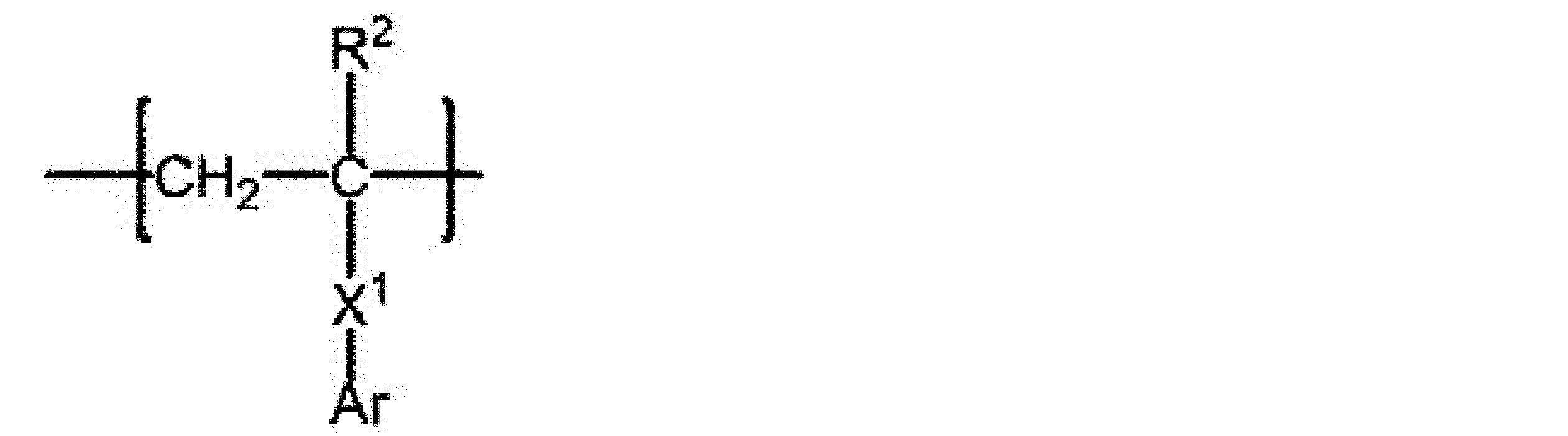
[式中、
R2は、ハロゲン原子を有してもよい炭素数1~6のアルキル基、水素原子又はハロゲン原子を表し、X1は、単結合、-CO-O-*又は-CO-NR4-*を表し、*は-Arとの結合手を表し、R4は、水素原子又は炭素数1~4のアルキル基を表し、Arは、ヒドロキシ基及びカルボキシル基からなる群から選ばれる1以上の基を有していてもよい炭素数6~20の芳香族炭化水素基を表す。] [In the formula,
R 2 represents an alkyl group having 1 to 6 carbon atoms which may have a halogen atom, a hydrogen atom or a halogen atom, X 1 is a single bond, -CO-O-* or -CO-NR 4 -* * represents a bond with -Ar, R 4 represents a hydrogen atom or an alkyl group having 1 to 4 carbon atoms, Ar is one or more groups selected from the group consisting of a hydroxy group and a carboxyl group represents an aromatic hydrocarbon group having 6 to 20 carbon atoms which may have ]
レジスト膜としては、例えば、以下が挙げられる。
Examples of resist films include the following.
下記式(a1)で表される繰り返し単位及び/又は下記式(a2)で表される繰り返し単位と、露光によりポリマー主鎖に結合した酸を発生する繰り返し単位とを含むベース樹脂を含むレジスト膜。
A resist film containing a base resin containing a repeating unit represented by the following formula (a1) and/or a repeating unit represented by the following formula (a2), and a repeating unit that is bonded to a polymer main chain and generates an acid upon exposure. .
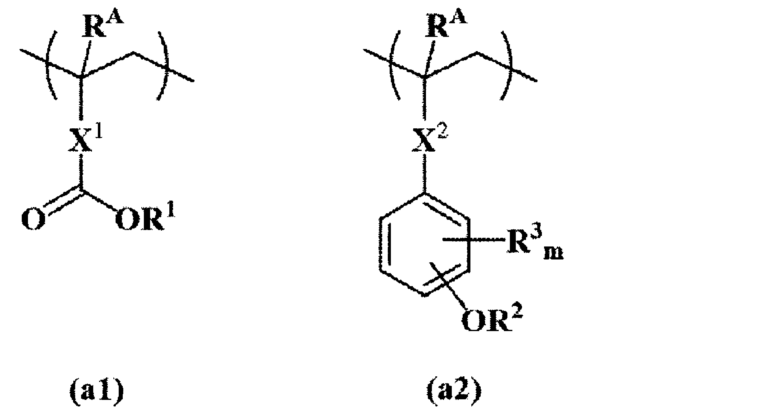
(式(a1)及び式(a2)中、RAは、それぞれ独立に、水素原子又はメチル基である。R1及びR2は、それぞれ独立に、炭素数4~6の3級アルキル基である。R3は、それぞれ独立に、フッ素原子又はメチル基である。mは、0~4の整数である。X1は、単結合、フェニレン基若しくはナフチレン基、又はエステル結合、ラクトン環、フェニレン基及びナフチレン基から選ばれる少なくとも1種を含む炭素数1~12の連結基である。X2は、単結合、エステル結合又はアミド結合である。)
(In formulas (a1) and (a2), R A is each independently a hydrogen atom or a methyl group; R 1 and R 2 are each independently a tertiary alkyl group having 4 to 6 carbon atoms; Each R 3 is independently a fluorine atom or a methyl group, m is an integer of 0 to 4, X 1 is a single bond, a phenylene group or a naphthylene group, an ester bond, a lactone ring, or a phenylene is a linking group having 1 to 12 carbon atoms and containing at least one selected from a group and a naphthylene group, and X 2 is a single bond, an ester bond or an amide bond.)
レジスト材料としては、例えば、以下が挙げられる。
Examples of resist materials include the following.
下記式(b1)又は式(b2)で表される繰り返し単位を有するポリマーを含むレジスト材料。
A resist material containing a polymer having a repeating unit represented by formula (b1) or formula (b2) below.

(式(b1)及び式(b2)中、RAは、水素原子又はメチル基である。X1は、単結合又はエステル基である。X2は、直鎖状、分岐状若しくは環状の炭素数1~12のアルキレン基又は炭素数6~10のアリーレン基であり、該アルキレン基を構成するメチレン基の一部が、エーテル基、エステル基又はラクトン環含有基で置換されていてもよく、また、X2に含まれる少なくとも1つの水素原子が臭素原子で置換されている。X3は、単結合、エーテル基、エステル基、又は炭素数1~12の直鎖状、分岐状若しくは環状のアルキレン基であり、該アルキレン基を構成するメチレン基の一部が、エーテル基又はエステル基で置換されていてもよい。Rf1~Rf4は、それぞれ独立に、水素原子、フッ素原子又はトリフルオロメチル基であるが、少なくとも1つはフッ素原子又はトリフルオロメチル基である。また、Rf1及びRf2が合わさってカルボニル基を形成してもよい。R1~R5は、それぞれ独立に、直鎖状、分岐状若しくは環状の炭素数1~12のアルキル基、直鎖状、分岐状若しくは環状の炭素数2~12のアルケニル基、炭素数2~12のアルキニル基、炭素数6~20のアリール基、炭素数7~12のアラルキル基、又は炭素数7~12のアリールオキシアルキル基であり、これらの基の水素原子の一部又は全部が、ヒドロキシ基、カルボキシ基、ハロゲン原子、オキソ基、シアノ基、アミド基、ニトロ基、スルトン基、スルホン基又はスルホニウム塩含有基で置換されていてもよく、これらの基を構成するメチレン基の一部が、エーテル基、エステル基、カルボニル基、カーボネート基又はスルホン酸エステル基で置換されていてもよい。また、R1とR2とが結合して、これらが結合する硫黄原子と共に環を形成してもよい。)
(In formula (b1) and formula (b2), R A is a hydrogen atom or a methyl group. X 1 is a single bond or an ester group. X 2 is a linear, branched or cyclic carbon an alkylene group having 1 to 12 carbon atoms or an arylene group having 6 to 10 carbon atoms, and part of the methylene groups constituting the alkylene group may be substituted with an ether group, an ester group or a lactone ring-containing group, In addition, at least one hydrogen atom contained in X 2 is substituted with a bromine atom, and X 3 is a single bond, an ether group, an ester group, or a linear, branched or cyclic group having 1 to 12 carbon atoms. an alkylene group, part of the methylene groups constituting the alkylene group may be substituted with an ether group or an ester group, and each of Rf 1 to Rf 4 independently represents a hydrogen atom, a fluorine atom or a trifluoro a methyl group, at least one of which is a fluorine atom or a trifluoromethyl group, and Rf 1 and Rf 2 may combine to form a carbonyl group, and R 1 to R 5 each independently linear, branched or cyclic alkyl groups having 1 to 12 carbon atoms, linear, branched or cyclic alkenyl groups having 2 to 12 carbon atoms, alkynyl groups having 2 to 12 carbon atoms, and 6 to 20 carbon atoms an aryl group, an aralkyl group having 7 to 12 carbon atoms, or an aryloxyalkyl group having 7 to 12 carbon atoms, and some or all of the hydrogen atoms of these groups are hydroxy groups, carboxy groups, halogen atoms, oxo group, cyano group, amido group, nitro group, sultone group, sulfone group or sulfonium salt-containing group, and some of the methylene groups constituting these groups are ether groups, ester groups and carbonyl groups. , may be substituted with a carbonate group or a sulfonate ester group.In addition, R 1 and R 2 may combine to form a ring together with the sulfur atom to which they are bonded.)
下記式(a)で表される繰り返し単位を含むポリマーを含むベース樹脂を含むレジスト材料。
A resist material containing a base resin containing a polymer containing a repeating unit represented by the following formula (a).

(式(a)中、RAは、水素原子又はメチル基である。R1は、水素原子又は酸不安定基である。R2は、直鎖状、分岐状若しくは環状の炭素数1~6のアルキル基、又は臭素以外のハロゲン原子である。X1は、単結合若しくはフェニレン基、又はエステル基若しくはラクトン環を含んでいてもよい直鎖状、分岐状若しくは環状の炭素数1~12のアルキレン基である。X2は、-O-、-O-CH2-又は-NH-である。mは、1~4の整数である。nは、0~3の整数である。)
露光により酸を発生し、酸の作用により現像液に対する溶解性が変化するレジスト組成物であって、
酸の作用により現像液に対する溶解性が変化する基材成分(A)及びアルカリ現像液に対して分解性を示すフッ素添加剤成分(F)を含有し、
前記フッ素添加剤成分(F)は、塩基解離性基を含む構成単位(f1)と、下記一般式(f2-r-1)で表される基を含む構成単位(f2)と、を有するフッ素樹脂成分(F1)を含有することを特徴とする、レジスト組成物。 (In formula (a), R A is a hydrogen atom or a methyl group. R 1 is a hydrogen atom or an acid labile group. R 2 is a linear, branched or cyclic C 1 to 6 alkyl groups or halogen atoms other than bromine, X 1 is a single bond or a phenylene group, or a linear, branched or cyclic C 1-12 group which may contain an ester group or a lactone ring is an alkylene group of X 2 is -O-, -O-CH 2 - or -NH-, m is an integer of 1 to 4, and n is an integer of 0 to 3.)
A resist composition that generates acid upon exposure and whose solubility in a developer changes due to the action of the acid,
Containing a base component (A) whose solubility in a developer changes under the action of an acid and a fluorine additive component (F) which exhibits decomposability in an alkaline developer,
The fluorine additive component (F) has a structural unit (f1) containing a base dissociable group and a structural unit (f2) containing a group represented by the following general formula (f2-r-1): fluorine A resist composition comprising a resin component (F1).

[式(f2-r-1)中、Rf21は、それぞれ独立に、水素原子、アルキル基、アルコキシ基、水酸基、ヒドロキシアルキル基又はシアノ基である。n”は、0~2の整数である。*は結合手である。]
[In formula (f2-r-1), each Rf 21 is independently a hydrogen atom, an alkyl group, an alkoxy group, a hydroxyl group, a hydroxyalkyl group, or a cyano group. n" is an integer of 0 to 2. * is a bond.]
前記構成単位(f1)は、下記一般式(f1-1)で表される構成単位、又は下記一般式(f1-2)で表される構成単位を含む。
The structural unit (f1) includes a structural unit represented by the following general formula (f1-1) or a structural unit represented by the following general formula (f1-2).
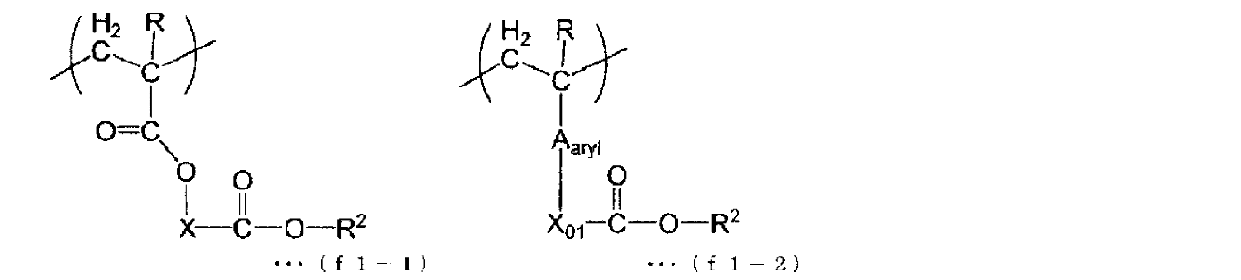
[式(f1-1)、(f1-2)中、Rは、それぞれ独立に、水素原子、炭素数1~5のアルキル基又は炭素数1~5のハロゲン化アルキル基である。Xは、酸解離性部位を有さない2価の連結基である。Aarylは、置換基を有していてもよい2価の芳香族環式基である。X01は、単結合又は2価の連結基である。R2は、それぞれ独立に、フッ素原子を有する有機基である。]
[In formulas (f1-1) and (f1-2), each R is independently a hydrogen atom, an alkyl group having 1 to 5 carbon atoms, or a halogenated alkyl group having 1 to 5 carbon atoms. X is a divalent linking group having no acid-labile site. A aryl is an optionally substituted divalent aromatic cyclic group. X 01 is a single bond or a divalent linking group. Each R 2 is independently an organic group having a fluorine atom. ]
コーティング、コーティング溶液、及びコーティング組成物としては、例えば、以下が挙げられる。
Examples of coatings, coating solutions, and coating compositions include the following.
金属炭素結合および/または金属カルボキシラート結合により有機配位子を有する金属オキソ-ヒドロキソネットワークを含むコーティング。
A coating containing a metal oxo-hydroxo network with organic ligands via metal carbon bonds and/or metal carboxylate bonds.
無機オキソ/ヒドロキソベースの組成物。
An inorganic oxo/hydroxo-based composition.
コーティング溶液であって、有機溶媒;第一の有機金属組成物であって、式RzSnO(2-(z/2)-(x/2))(OH)x(ここで、0<z≦2および0<(z+x)≦4である)、式R’nSnX4-n(ここで、n=1または2である)、またはそれらの混合物によって表され、ここで、RおよびR’が、独立して、1~31個の炭素原子を有するヒドロカルビル基であり、およびXが、Snに対する加水分解性結合を有する配位子またはそれらの組合せである、第一の有機金属組成物;および加水分解性の金属化合物であって、式MX’v(ここで、Mが、元素周期表の第2~16族から選択される金属であり、v=2~6の数であり、およびX’が、加水分解性のM-X結合を有する配位子またはそれらの組合せである)によって表される、加水分解性の金属化合物を含む、コーティング溶液。
a coating solution comprising an organic solvent; a first organometallic composition comprising the formula R z SnO (2-(z/2)-(x/2)) (OH) x where 0<z ≦2 and 0<(z+x)≦4), represented by the formula R′ n SnX 4-n where n=1 or 2, or mixtures thereof, where R and R′ is independently a hydrocarbyl group having from 1 to 31 carbon atoms, and X is a ligand or combination thereof having a hydrolyzable bond to Sn; and a hydrolyzable metal compound of formula MX' v , where M is a metal selected from Groups 2-16 of the Periodic Table of the Elements, v=a number from 2 to 6, and X′ is a ligand or combination thereof having a hydrolyzable MX bond.
有機溶媒と、式RSnO(3/2-x/2)(OH)x(式中、0<x<3)で表される第1の有機金属化合物とを含むコーティング溶液であって、前記溶液中に約0.0025M~約1.5Mのスズが含まれ、Rが3~31個の炭素原子を有するアルキル基またはシクロアルキル基であり、前記アルキル基またはシクロアルキル基が第2級または第3級炭素原子においてスズに結合された、コーティング溶液。
A coating solution comprising an organic solvent and a first organometallic compound represented by the formula RSnO (3/2-x/2) (OH) x where 0<x<3, wherein the solution from about 0.0025M to about 1.5M tin, and R is an alkyl or cycloalkyl group having 3 to 31 carbon atoms, wherein said alkyl or cycloalkyl group is a secondary or secondary A coating solution bonded to tin at a tertiary carbon atom.
水と、金属亜酸化物陽イオンと、多原子無機陰イオンと、過酸化物基を含んで成る感放射線リガンドとの混合物を含んで成る無機パターン形成前駆体水溶液。
An aqueous inorganic pattern-forming precursor comprising a mixture of water, a metal suboxide cation, a polyatomic inorganic anion, and a radiation-sensitive ligand comprising a peroxide group.
露光は、所定のパターンを形成するためのマスク(レチクル)を通して行われ、例えば、i線、KrFエキシマレーザー、ArFエキシマレーザー、EUV(極端紫外線)またはEB(電子線)が使用されるが、本願のレジスト下層膜形成組成物は、EB(電子線)又はEUV(極端紫外線)露光用に適用されることが好ましく、EUV(極端紫外線)露光用に適用されることが好ましい。現像にはアルカリ現像液が用いられ、現像温度5℃~50℃、現像時間10秒~300秒から適宜選択される。アルカリ現像液としては、例えば、水酸化ナトリウム、水酸化カリウム、炭酸ナトリウム、ケイ酸ナトリウム、メタケイ酸ナトリウム、アンモニア水等の無機アルカリ類、エチルアミン、n-プロピルアミン等の第一アミン類、ジエチルアミン、ジ-n-ブチルアミン等の第二アミン類、トリエチルアミン、メチルジエチルアミン等の第三アミン類、ジメチルエタノールアミン、トリエタノールアミン等のアルコールアミン類、テトラメチルアンモニウムヒドロキシド、テトラエチルアンモニウムヒドロキシド、コリン等の第4級アンモニウム塩、ピロール、ピペリジン等の環状アミン類、等のアルカリ類の水溶液を使用することができる。さらに、上記アルカリ類の水溶液にイソプロピルアルコール等のアルコール類、ノニオン系等の界面活性剤を適当量添加して使用することもできる。これらの中で好ましい現像液は第四級アンモニウム塩、さらに好ましくはテトラメチルアンモニウムヒドロキシド及びコリンである。さらに、これらの現像液に界面活性剤などを加えることもできる。アルカリ現像液に代えて、酢酸ブチル等の有機溶媒で現像を行い、フォトレジストのアルカリ溶解速度が向上していない部分を現像する方法を用いることもできる。上記工程を経て、上記レジストがパターンニングされた基板が製造できる。
Exposure is performed through a mask (reticle) for forming a predetermined pattern, and for example, i-ray, KrF excimer laser, ArF excimer laser, EUV (extreme ultraviolet) or EB (electron beam) is used. is preferably applied for EB (electron beam) or EUV (extreme ultraviolet) exposure, and preferably for EUV (extreme ultraviolet) exposure. An alkaline developer is used for development, and the development temperature is selected from 5° C. to 50° C. and the development time is appropriately selected from 10 seconds to 300 seconds. Examples of the alkaline developer include inorganic alkalis such as sodium hydroxide, potassium hydroxide, sodium carbonate, sodium silicate, sodium metasilicate, aqueous ammonia, primary amines such as ethylamine and n-propylamine, diethylamine, secondary amines such as di-n-butylamine; tertiary amines such as triethylamine and methyldiethylamine; alcohol amines such as dimethylethanolamine and triethanolamine; Aqueous solutions of alkalis such as quaternary ammonium salts, pyrrole, cyclic amines such as piperidine, and the like can be used. Further, an alcohol such as isopropyl alcohol or a nonionic surfactant may be added in an appropriate amount to the aqueous alkali solution. Preferred developers among these are quaternary ammonium salts, more preferably tetramethylammonium hydroxide and choline. Furthermore, a surfactant or the like can be added to these developers. It is also possible to use a method of developing with an organic solvent such as butyl acetate instead of the alkaline developer, and developing the portion where the rate of alkali dissolution of the photoresist is not improved. Through the above steps, a substrate having the resist patterned thereon can be manufactured.
次いで、形成したレジストパターンをマスクとして、前記レジスト下層膜をドライエッチングする。その際、用いた半導体基板の表面に前記無機膜が形成されている場合、その無機膜の表面を露出させ、用いた半導体基板の表面に前記無機膜が形成されていない場合、その半導体基板の表面を露出させる。その後基板を自体公知の方法(ドライエッチング法等)により基板を加工する工程を経て、半導体装置が製造できる。
Then, using the formed resist pattern as a mask, the resist underlayer film is dry-etched. At that time, when the inorganic film is formed on the surface of the semiconductor substrate used, the surface of the inorganic film is exposed, and when the inorganic film is not formed on the surface of the semiconductor substrate used, the semiconductor substrate is exposed. expose the surface. After that, the substrate is processed by a method known per se (dry etching method, etc.), and a semiconductor device can be manufactured.
<ウエハ端部保護膜を形成する工程を含む半導体装置の製造方法>
本発明に係る光硬化性樹脂組成物は、半導体製造用ウエハ端部保護膜を形成するために用いることもできる。
以下に、本発明に係る光硬化性樹脂組成物を、半導体製造用ウエハ端部保護膜を形成するために使用する場合について説明する。 <Method for Manufacturing Semiconductor Device Including Step of Forming Wafer Edge Protection Film>
The photocurable resin composition according to the present invention can also be used to form a wafer edge protection film for semiconductor manufacturing.
A case of using the photocurable resin composition according to the present invention to form a wafer edge protection film for semiconductor manufacturing will be described below.
本発明に係る半導体装置の製造方法は、
(A) 半導体基板上にレジスト膜を形成する工程と、
(B) レジスト膜に対する光又は電子線の照射とその後の現像によりレジストパターンを形成する工程と、
(C) 半導体基板をエッチングで加工する工程と、
を含む半導体装置の製造方法において、
半導体製造用ウエハの表面端部と、任意選択的にベベル部及び/又は裏面端部に、
本発明に係る光硬化性樹脂組成物からの保護膜を形成する工程(X)
を含む、
半導体装置の製造方法である。 A method for manufacturing a semiconductor device according to the present invention includes:
(A) forming a resist film on a semiconductor substrate;
(B) forming a resist pattern by irradiating the resist film with light or an electron beam and then developing;
(C) a step of etching the semiconductor substrate;
In a method of manufacturing a semiconductor device comprising
on the front edge and optionally the bevel and/or the back edge of a semiconductor fabrication wafer,
Step (X) of forming a protective film from the photocurable resin composition according to the present invention
including,
A method for manufacturing a semiconductor device.
以下、順に説明する。
[(A)半導体基板上にレジスト膜を形成する工程]
半導体基板上にレジスト膜を形成する。半導体基板は、半導体素子等の製造のために使用されるウエハであり、一般的に用いられるシリコンウェハー、ゲルマニウムウェハーの他、例えば、ヒ化ガリウム、リン化インジウム、窒化ガリウム、窒化インジウム、窒化アルミニウム等の2種類以上の元素が結合してできる化合物半導体ウエハが使用できる。これらは通常円盤状であり、大きさは例えば4、6、8、12インチ等である。市販品を使用してよい。 They will be described in order below.
[(A) Step of forming a resist film on a semiconductor substrate]
A resist film is formed on a semiconductor substrate. Semiconductor substrates are wafers used for the manufacture of semiconductor devices and the like, and include commonly used silicon wafers, germanium wafers, gallium arsenide, indium phosphide, gallium nitride, indium nitride, and aluminum nitride. A compound semiconductor wafer formed by combining two or more kinds of elements such as They are usually disc-shaped and have sizes of, for example, 4, 6, 8, 12 inches, and the like. Commercial products may be used.
表面に無機膜が形成された半導体基板を用いる場合、当該無機膜は、例えば、ALD(原子層堆積)法、CVD(化学気相堆積)法、反応性スパッタ法、イオンプレーティング法、真空蒸着法、スピンコーティング法(スピンオングラス:SOG)により形成される。前記無機膜として、例えば、ポリシリコン膜、酸化ケイ素膜、窒化珪素膜、BPSG(Boro-Phospho Silicate Glass)膜、窒化チタン膜、窒化酸化チタン膜、タングステン膜、窒化ガリウム膜、及びヒ化ガリウム膜が挙げられる。
When using a semiconductor substrate having an inorganic film formed on its surface, the inorganic film is formed by, for example, an ALD (atomic layer deposition) method, a CVD (chemical vapor deposition) method, a reactive sputtering method, an ion plating method, or a vacuum deposition method. It is formed by a spin coating method (spin on glass: SOG). Examples of the inorganic film include a polysilicon film, a silicon oxide film, a silicon nitride film, a BPSG (Boro-Phospho Silicate Glass) film, a titanium nitride film, a titanium oxynitride film, a tungsten film, a gallium nitride film, and a gallium arsenide film. is mentioned.
このような半導体基板上に、スプレー、スピナー、コーター等の適当な塗布方法により所定の厚みのレジスト下層膜、レジスト膜等を形成する。一般に回転塗布法の場合、レジスト下層膜形成組成物、レジスト膜形成組成物等のそれぞれが、回転する円盤状基板の中心部の上方からノズル等を通じて供給される。通常、これらの膜は、ホットプレート等の加熱手段を用いてベークする。
A resist underlayer film, a resist film, etc., having a predetermined thickness are formed on such a semiconductor substrate by an appropriate coating method such as a spray, spinner, or coater. Generally, in the spin coating method, each of the resist underlayer film-forming composition, the resist film-forming composition, and the like is supplied through a nozzle or the like from above the central portion of the rotating disk-shaped substrate. These films are typically baked using a heating means such as a hot plate.
回転塗布法により膜厚300nm程度の保護膜を作製するためには、保護膜形成用組成物としての本発明に係る光硬化性樹脂組成物は25℃において約100cps以下の粘度を有することが好ましい。なお、本発明において、粘度は、E型粘度計による測定値である。
In order to form a protective film having a thickness of about 300 nm by spin coating, the photocurable resin composition according to the present invention as a composition for forming a protective film preferably has a viscosity of about 100 cps or less at 25°C. . In addition, in this invention, a viscosity is a measured value by an E-type viscometer.
レジスト膜の形成に使用されるフォトレジストとしては、露光に使用される光に感光するものであれば特に限定はない。ネガ型フォトレジスト及びポジ型フォトレジストのいずれも使用できる。ノボラック樹脂と1,2-ナフトキノンジアジドスルホン酸エステルとからなるポジ型フォトレジスト、酸により分解してアルカリ溶解速度を上昇させる基を有するバインダーと光酸発生剤からなる化学増幅型フォトレジスト、酸により分解してフォトレジストのアルカリ溶解速度を上昇させる低分子化合物とアルカリ可溶性バインダーと光酸発生剤とからなる化学増幅型フォトレジスト、及び酸により分解してアルカリ溶解速度を上昇させる基を有するバインダーと酸により分解してフォトレジストのアルカリ溶解速度を上昇させる低分子化合物と光酸発生剤からなる化学増幅型フォトレジスト、メタル元素を含有するレジストなどがある。例えば、JSR(株)製商品名V146G、シプレー社製商品名APEX-E、住友化学工業(株)製商品名PAR710、及び信越化学工業(株)製商品名AR2772、SEPR430等が挙げられる。また、例えば、Proc.SPIE,Vol.3999,330-334(2000)、Proc.SPIE,Vol.3999,357-364(2000)、やProc.SPIE,Vol.3999,365-374(2000)に記載されているような、含フッ素原子ポリマー系フォトレジストを挙げることができる。好ましくはネガ型フォトレジストである。
The photoresist used for forming the resist film is not particularly limited as long as it is sensitive to the light used for exposure. Both negative and positive photoresists can be used. positive photoresist composed of novolac resin and 1,2-naphthoquinonediazide sulfonic acid ester; A chemically amplified photoresist comprising a low-molecular compound that decomposes to increase the alkali dissolution rate of the photoresist, an alkali-soluble binder, and a photoacid generator, and a binder having a group that decomposes with an acid to increase the alkali dissolution rate. There are chemically amplified photoresists composed of low-molecular-weight compounds and photoacid generators that are decomposed by acid to increase the rate of alkali dissolution of photoresists, and resists containing metal elements. Examples include V146G (trade name) manufactured by JSR Corporation, APEX-E (trade name) manufactured by Shipley, PAR710 (trade name) manufactured by Sumitomo Chemical Co., Ltd., AR2772 (trade name) and SEPR430 (trade name) manufactured by Shin-Etsu Chemical Co., Ltd., and the like. Also, for example, Proc. SPIE, Vol. 3999, 330-334 (2000), Proc. SPIE, Vol. 3999, 357-364 (2000), and Proc. SPIE, Vol. 3999, 365-374 (2000). A negative photoresist is preferred.
レジスト膜の形成に使用されるレジスト膜形成組成物には、一種以上の金属を含めることができる。金属の形態としては、金属単体のほか、金属塩、金属錯体、その他の金属含有化合物が挙げられる。金属種としては特に限定されないが、例えば、スズ、インジウム、アンチモン、ビスマス、ガリウム、ゲルマニウム、アルミニウム、ジルコニウム、ハフニウム、セリウム、ランタン、セシウム等が挙げられる。
The resist film-forming composition used for forming the resist film can contain one or more metals. Examples of the form of the metal include simple metals, metal salts, metal complexes, and other metal-containing compounds. Metal species are not particularly limited, but examples include tin, indium, antimony, bismuth, gallium, germanium, aluminum, zirconium, hafnium, cerium, lanthanum, and cesium.
レジスト膜のベーク条件としては、ベーク温度70℃~400℃、ベーク時間0.3分~60分間の中から適宜、選択される。好ましくは、ベーク温度80℃~350℃、ベーク時間0.5分~30分間、より好ましくは、ベーク温度90℃~300℃、ベーク時間0.8分~10分間である。
レジスト膜の平均厚さの下限は、好ましくは1nm、より好ましくは3nm、5nm、10nmである。レジスト膜の平均厚さの上限は、5,000nm、3,000nm、2,000nm、好ましくは1,000nm、より好ましくは500nm、200nm、更に好ましくは50nmである。 Baking conditions for the resist film are appropriately selected from a baking temperature of 70° C. to 400° C. and a baking time of 0.3 minutes to 60 minutes. Preferably, the baking temperature is 80° C. to 350° C., the baking time is 0.5 minutes to 30 minutes, and more preferably the baking temperature is 90° C. to 300° C., and the baking time is 0.8 minute to 10 minutes.
The lower limit of the average thickness of the resist film is preferably 1 nm, more preferably 3 nm, 5 nm and 10 nm. The upper limit of the average thickness of the resist film is 5,000 nm, 3,000 nm, 2,000 nm, preferably 1,000 nm, more preferably 500 nm, 200 nm, still more preferably 50 nm.
[保護膜を形成する工程(X)]
半導体製造用ウエハの表面端部と、任意選択的にベベル部及び/又は裏面端部に、光硬化性樹脂組成物からの保護膜を形成する工程(X)を任意の時点で行う。工程(X)においては、好ましくは、光硬化性樹脂組成物を塗布し、所定の領域に露光、現像を行う。工程(X)は、工程(A)の前に行ってもよく、工程(A)と工程(B)との間に行ってもよく、工程(B)又は工程(C)の後に行ってもよい。 [Step (X) of forming a protective film]
The step (X) of forming a protective film from the photocurable resin composition on the front edge and optionally the bevel and/or the back edge of the semiconductor manufacturing wafer is performed at any time. In step (X), preferably, a photocurable resin composition is applied, and a predetermined region is exposed and developed. Step (X) may be performed before step (A), between step (A) and step (B), or after step (B) or step (C). good.
なお、本願明細書において、基板のレジスト膜等のデバイス部が設けられた面を表面、その反対側の面を裏面という。また、表面端部とは、基板上に設けられたデバイス部の端からベベル部に至るまでの通常1~10mmの幅の領域をいい、ベベル部とは、表面端部と裏面端部をつなぐ曲がった領域をいい、裏面端部とは、基板裏面の表面端部に対応する領域をいう。
In the specification of the present application, the surface of the substrate on which the device portion such as the resist film is provided is called the front surface, and the opposite surface is called the back surface. In addition, the front surface edge refers to a region generally having a width of 1 to 10 mm from the edge of the device portion provided on the substrate to the bevel portion, and the bevel portion connects the front surface edge and the back surface edge. The bent area is defined as the edge of the rear surface, and the edge of the rear surface of the substrate is the area corresponding to the edge of the front surface of the rear surface of the substrate.
まず、レジスト膜等の形成された半導体基板に本発明に係る光硬化性樹脂組成物を施用する。光硬化性樹脂組成物を施用する方法としては、特に限定されないが、例えば、回転塗布法(スピンコート法)、スプレー法等の公知の手段を採用することができる。例えば、回転塗布法を採用する場合、レジスト膜等の形成された半導体基板を所定の回転速度で回転させつつ、光硬化性樹脂組成物を、回転する円盤状基板の表面端部の上方又は近傍からノズルを通じて供給する。好ましくは、当該基板のベベル部及び/又は裏面端部にも、各々の近傍からノズルを通じて供給する。
First, the photocurable resin composition according to the present invention is applied to a semiconductor substrate on which a resist film or the like is formed. The method of applying the photocurable resin composition is not particularly limited, but known means such as a spin coating method (spin coating method) and a spray method can be employed. For example, when a spin coating method is employed, while rotating a semiconductor substrate on which a resist film or the like is formed at a predetermined rotation speed, the photocurable resin composition is applied above or near the edge of the surface of the rotating disk-shaped substrate. through a nozzle from Preferably, the beveled portion and/or the backside edge of the substrate are also fed through the nozzle from the vicinity of each.
回転塗布の条件は適宜選択することができ、何ら限定されるものではないが、典型的な条件を例示すると以下のとおりである。
・光硬化性樹脂組成物の粘度:約100cps以下
・ウエハの回転速度:
・・光硬化性樹脂組成物供給時:50~500rpm
・・乾燥振り切り時:700~2,000rpm
・保護膜厚み:300nm The spin coating conditions can be selected as appropriate and are not limited at all, but typical conditions are as follows.
・Viscosity of photocurable resin composition: about 100 cps or less ・Wafer rotation speed:
.. When supplying the photocurable resin composition: 50 to 500 rpm
・・When drying and shaking off: 700 to 2,000 rpm
・Protective film thickness: 300 nm
次に、光硬化性樹脂組成物の露光を行う。露光は、光硬化性樹脂組成物に、マスクを介して、又はマスクを介さずに紫外線、可視光線、放射線などの活性光線(i線、KrFエキシマレーザー、ArFエキシマレーザー、EUV(極端紫外線)、EB(電子線)を含む)を照射することにより行うことができる。なお、露光前にソフトベーク(SB)を行ってもよく、露光後現像前に露光後加熱(PEB)を行ってもよい。露光後加熱の温度は50℃~150℃、露光後加熱の時間は1分~10分が好ましい。
好ましくは170~800nm(より好ましくは200~600nm、更に好ましくは300~500nm)の波長の光で光硬化性樹脂組成物を硬化させる。 Next, the photocurable resin composition is exposed. The photocurable resin composition is exposed to actinic rays such as ultraviolet rays, visible rays, and radiation (i-ray, KrF excimer laser, ArF excimer laser, EUV (extreme ultraviolet rays), through a mask or without a mask. EB (including electron beam)) can be applied. Note that soft baking (SB) may be performed before exposure, and post-exposure baking (PEB) may be performed after exposure and before development. The post-exposure heating temperature is preferably 50° C. to 150° C., and the post-exposure heating time is preferably 1 to 10 minutes.
The photocurable resin composition is cured with light having a wavelength of preferably 170 to 800 nm (more preferably 200 to 600 nm, still more preferably 300 to 500 nm).
次に、露光後の光硬化性樹脂組成物の現像を行う。現像は、露光後の光硬化性樹脂組成物の露光部を現像液で除去することにより行うことができ、現像温度5℃~50℃、現像時間10秒~300秒から適宜選択される。
Next, the photocurable resin composition after exposure is developed. Development can be carried out by removing the exposed portion of the photocurable resin composition after exposure with a developer, and the development temperature is appropriately selected from 5° C. to 50° C. and the development time is selected from 10 seconds to 300 seconds.
現像液に含有される有機溶媒としては、例えばアルコール系溶媒、エーテル系溶媒、ケトン系溶媒、アミド系溶媒、エステル系溶媒、炭化水素系溶媒等が挙げられる。上記現像液の有機溶媒としては、エステル系溶媒、ケトン系溶媒又はこれらの組み合わせを含むものが好ましい。上記現像液は、有機溶媒を1種単独で含有していてもよく、2種以上を含有していてもよい。
Examples of organic solvents contained in the developer include alcohol solvents, ether solvents, ketone solvents, amide solvents, ester solvents, hydrocarbon solvents, and the like. As the organic solvent for the developer, those containing an ester solvent, a ketone solvent, or a combination thereof are preferable. The developer may contain one type of organic solvent alone, or may contain two or more types.
アルコール系溶媒としては、例えば、4-メチル-2-ペンタノール、n-ヘキサノール等の炭素数1~18の脂肪族モノアルコール系溶媒;シクロヘキサノール等の炭素数3~18の脂環式モノアルコール系溶媒;プロピレングリコールモノメチルエーテル等の炭素数3~19の多価アルコール部分エーテル系溶媒などが挙げられる。
Examples of alcohol solvents include aliphatic monoalcohol solvents having 1 to 18 carbon atoms such as 4-methyl-2-pentanol and n-hexanol; alicyclic monoalcohols having 3 to 18 carbon atoms such as cyclohexanol. system solvent; polyhydric alcohol partial ether system solvent having 3 to 19 carbon atoms such as propylene glycol monomethyl ether.
エーテル系溶媒としては、例えば、ジエチルエーテル、ジプロピルエーテル、ジブチルエーテル、ジペンチルエーテル、ジイソアミルエーテル、ジヘキシルエーテル、ジヘプチルエーテル等のジアルキルエーテル系溶媒;テトラヒドロフラン、テトラヒドロピラン等の環状エーテル系溶媒;ジフェニルエーテル、アニソール等の芳香環含有エーテル系溶媒などが挙げられる。
Examples of ether solvents include dialkyl ether solvents such as diethyl ether, dipropyl ether, dibutyl ether, dipentyl ether, diisoamyl ether, dihexyl ether, and diheptyl ether; cyclic ether solvents such as tetrahydrofuran and tetrahydropyran; and diphenyl ether. and aromatic ring-containing ether solvents such as anisole.
ケトン系溶媒としては、例えば、アセトン、メチルエチルケトン、メチル-n-プロピルケトン、メチル-n-ブチルケトン、ジエチルケトン、メチル-iso-ブチルケトン、2-ヘプタノン、エチル-n-ブチルケトン、メチル-n-ヘキシルケトン、ジ-iso-ブチルケトン、トリメチルノナノン等の鎖状ケトン系溶媒:シクロペンタノン、シクロヘキサノン、シクロヘプタノン、シクロオクタノン、メチルシクロヘキサノン等の環状ケトン系溶媒:2,4-ペンタンジオン、アセトニルアセトン、アセトフェノン等が挙げられる。
Ketone solvents include, for example, acetone, methyl ethyl ketone, methyl-n-propyl ketone, methyl-n-butyl ketone, diethyl ketone, methyl-iso-butyl ketone, 2-heptanone, ethyl-n-butyl ketone, methyl-n-hexyl ketone. , di-iso-butyl ketone, trimethylnonanone and other chain ketone solvents: cyclopentanone, cyclohexanone, cycloheptanone, cyclooctanone, methylcyclohexanone and other cyclic ketone solvents: 2,4-pentanedione, acetonyl Acetone, acetophenone, and the like.
アミド系溶媒としては、例えば、N,N’-ジメチルイミダゾリジノン、N-メチルピロリドン等の環状アミド系溶媒;N-メチルホルムアミド、N,N-ジメチルホルムアミド、N,N-ジエチルホルムアミド、アセトアミド、N-メチルアセトアミド、N,N-ジメチルアセトアミド、N-メチルプロピオンアミド等の鎖状アミド系溶媒などが挙げられる。
Examples of amide solvents include cyclic amide solvents such as N,N'-dimethylimidazolidinone and N-methylpyrrolidone; N-methylformamide, N,N-dimethylformamide, N,N-diethylformamide, acetamide, Chain amide solvents such as N-methylacetamide, N,N-dimethylacetamide, N-methylpropionamide and the like are included.
エステル系溶媒としては、例えば、酢酸n-ブチル、乳酸エチル等のモノカルボン酸エステル系溶媒;プロピレングリコールアセテート等の多価アルコールカルボキシレート系溶媒;プロピレングリコールモノメチルエーテルアセテート等の多価アルコール部分エーテルカルボキシレート系溶媒;シュウ酸ジエチル等の多価カルボン酸ジエステル系溶媒;ジメチルカーボネート、ジエチルカーボネート等のカーボネート系溶媒などが挙げられる。
Examples of ester solvents include monocarboxylic acid ester solvents such as n-butyl acetate and ethyl lactate; polyhydric alcohol carboxylate solvents such as propylene glycol acetate; polyhydric alcohol partial ether carboxylates such as propylene glycol monomethyl ether acetate; rate-based solvents; polyvalent carboxylic acid diester-based solvents such as diethyl oxalate; and carbonate-based solvents such as dimethyl carbonate and diethyl carbonate.
炭化水素系溶媒としては、例えば、n-ペンタン、n-ヘキサン等の炭素数5~12の脂肪族炭化水素系溶媒;トルエン、キシレン等の炭素数6~16の芳香族炭化水素系溶媒等が挙げられる。
Examples of hydrocarbon solvents include aliphatic hydrocarbon solvents having 5 to 12 carbon atoms such as n-pentane and n-hexane; aromatic hydrocarbon solvents having 6 to 16 carbon atoms such as toluene and xylene. mentioned.
これらの中では、エステル系溶媒、ケトン系溶媒、エーテル系溶媒及びこれらの組み合わせが好ましく、エステル系溶媒、ケトン系溶媒及びこれらの組み合わせがより好ましい。エステル系溶媒としては、プロピレングリコールモノメチルエーテルアセテートが好ましい。ケトン系溶媒としては、シクロヘキサノンが好ましい。エーテル系溶媒としては、プロピレングリコールモノメチルエーテルが好ましい。
Among these, ester-based solvents, ketone-based solvents, ether-based solvents, and combinations thereof are preferred, and ester-based solvents, ketone-based solvents, and combinations thereof are more preferred. As the ester solvent, propylene glycol monomethyl ether acetate is preferred. Cyclohexanone is preferred as the ketone solvent. Propylene glycol monomethyl ether is preferable as the ether solvent.
現像液中の有機溶媒の含有量の下限としては、80質量%が好ましく、90質量%がより好ましく、99質量%がさらに好ましく、100質量%が特に好ましい。現像液中の有機溶媒の含有量を上記範囲とすることで、露光部と未露光部との間の溶解コントラストを向上させることができ、その結果、リソグラフィー性能により優れたレジストパターンを形成することができる。有機溶媒以外の成分としては、例えば水、シリコンオイル等が挙げられる。
The lower limit of the content of the organic solvent in the developer is preferably 80% by mass, more preferably 90% by mass, even more preferably 99% by mass, and particularly preferably 100% by mass. By setting the content of the organic solvent in the developer within the above range, the dissolution contrast between the exposed area and the unexposed area can be improved, and as a result, a resist pattern with excellent lithography performance can be formed. can be done. Components other than the organic solvent include, for example, water and silicon oil.
現像液は含窒素化合物を含有していてもよい。上記現像液が含窒素化合物を含有することで、形成されるレジストパターンにおける膜減りをより低減させることができる。
The developer may contain a nitrogen-containing compound. When the developer contains a nitrogen-containing compound, it is possible to further reduce film loss in the formed resist pattern.
現像液は、上記の有機溶媒系現像液に替えて、水溶液の現像液を使用してもよい。具体的には、水酸化ナトリウム、水酸化カリウム、ケイ酸ナトリウム、アンモニア、モノエチルアミン、ジエチルアミン、トリエチルアミン、トリエタノールアミン、水酸化テトラメチルアンモニウムなどのアルカリ水溶液等であってもよい。これらの水溶液の塩基濃度は特に限定されないが、例えば、0.1~10質量%とすることができる。
As the developer, an aqueous developer may be used instead of the organic solvent-based developer described above. Specifically, alkaline aqueous solutions such as sodium hydroxide, potassium hydroxide, sodium silicate, ammonia, monoethylamine, diethylamine, triethylamine, triethanolamine, and tetramethylammonium hydroxide may be used. The base concentration of these aqueous solutions is not particularly limited, but can be, for example, 0.1 to 10% by mass.
また、上記現像液にアルコール類や界面活性剤を添加して使用することもできる。これらはそれぞれ、現像液100重量部に対して、好ましくは0.01~10重量部、より好ましくは0.1~5重量部の範囲で配合することができる。界面活性剤としては、例えばイオン性や非イオン性のフッ素系界面活性剤、シリコン系界面活性剤等が挙げられる。
In addition, alcohols and surfactants can be added to the developer and used. Each of these can be blended in the range of preferably 0.01 to 10 parts by weight, more preferably 0.1 to 5 parts by weight, per 100 parts by weight of the developer. Examples of surfactants include ionic and nonionic fluorine-based surfactants, silicon-based surfactants, and the like.
現像方法としては、例えば現像液が満たされた槽中に基板を一定時間浸漬する方法(ディップ法)、基板表面に現像液を表面張力によって盛り上げて一定時間静止することで現像する方法(パドル法)、基板表面に現像液を噴霧する方法(スプレー法)、一定速度で回転している基板上に一定速度で現像液塗出ノズルをスキャンしながら現像液を塗出しつづける方法(ダイナミックディスペンス法)等が挙げられる。
Examples of the development method include a method in which the substrate is immersed in a bath filled with a developer for a certain period of time (dip method), and a method in which the developer is piled up on the surface of the substrate by surface tension and left stationary for a certain period of time (paddle method). ), a method in which the developer is sprayed onto the surface of the substrate (spray method), and a method in which the developer dispensing nozzle scans the substrate rotating at a constant speed and continuously dispenses the developer (dynamic dispensing method). etc.
次に、現像後の光硬化性樹脂組成物のベーキングを行う。現像後得られたパターンをベークすることにより、所望のパターンを形成することができる。加熱処理における加熱温度は、通常150℃以上、350℃以下、好ましくは200~300℃の範囲である。加熱処理時間は、光硬化性樹脂組成物が硬化するまでの時間であり、生産性を考慮すると概ね30分未満であることが好ましい。
保護膜の平均厚さの下限は、例えば1nm、3nm、5nm、10nm、30nm、50nm、80nm、100nm、150nm、200nmである。保護膜の平均厚さの上限は、例えば10μm、8μm、5μm、3μm、1μm、800nm、500nm、300nmである。 Next, the photocurable resin composition after development is baked. A desired pattern can be formed by baking the pattern obtained after development. The heating temperature in the heat treatment is usually 150°C or higher and 350°C or lower, preferably 200 to 300°C. The heat treatment time is the time until the photocurable resin composition is cured, and is preferably less than 30 minutes in general in consideration of productivity.
The lower limits of the average thickness of the protective film are, for example, 1 nm, 3 nm, 5 nm, 10 nm, 30 nm, 50 nm, 80 nm, 100 nm, 150 nm and 200 nm. The upper limits of the average thickness of the protective film are, for example, 10 μm, 8 μm, 5 μm, 3 μm, 1 μm, 800 nm, 500 nm, and 300 nm.
半導体製造用基板(ウエハ)の端部を覆う保護膜の特性としては、ウエハ端部の金属汚染を防止する機能のほか、ドライエッチング耐性、リン酸耐性、水酸化テトラメチルアンモニウム(TMAH)耐性、HF除去性、耐擦傷性、段差基板に対する良好な埋め込み性、低昇華物量、疎水性基板に対する親和性、ウエハ側面にクレーター異物等を残さないこと、良好なエッジ形状、インナーハンプ(ノズルの射出孔直下に膜形成組成物が瘤状に残る現象)を抑制する機能等を満足することが望ましい。
The protective film that covers the edges of semiconductor manufacturing substrates (wafers) has properties such as the ability to prevent metal contamination on the edges of the wafer, as well as dry etching resistance, phosphoric acid resistance, tetramethylammonium hydroxide (TMAH) resistance, HF removability, scratch resistance, good embeddability for stepped substrates, low amount of sublimation, affinity for hydrophobic substrates, no crater foreign matter left on wafer side, good edge shape, inner hump (nozzle injection hole) It is desirable to satisfy the function of suppressing the phenomenon that the film-forming composition remains in the form of nodules immediately below.
また、本発明に係る光硬化性樹脂組成物は、上記基板の表面端部と、任意選択的にベベル部及び/又は裏面端部に、該感光性光硬化性樹脂組成物(ネガ型)を塗布した後、膜の硬化を行いたい部分を露光、現像を行うことで、ベベル部分を正確に前記保護膜で覆うことが可能となる。感光性であることにより、保護膜のウエハ端面における膜厚コントロールが容易となり、インナーハンプを除去することができ、エッジ形状を改良することができ、回転塗布時のセンターポジションのずれを修正できる等の利点がある。
In addition, the photocurable resin composition according to the present invention is provided by applying the photosensitive photocurable resin composition (negative type) to the front surface edge portion of the substrate and optionally to the bevel portion and/or the back surface edge portion. After coating, the bevel portion can be accurately covered with the protective film by exposing and developing the portion of the film to be cured. Photosensitivity makes it easy to control the film thickness of the protective film on the wafer edge, remove the inner hump, improve the edge shape, and correct the deviation of the center position during spin coating. has the advantage of
工程(X)の後に、工程(Y)において、保護膜の上の部分のレジスト膜は、除去液により除去することができる。このとき、上記工程(X)と同様に、半導体製造用ウエハの表面端部と、任意選択的にベベル部及び/又は裏面端部に除去液を適用することが好ましい。レジスト除去液としては、例えば、プロピレングリコールモノメチルエーテル、プロピレングリコールモノメチルエーテルアセテート、シクロヘキサノン、水、酢酸ブチル、テトラメチルアンモニウム水溶液またはそれらの組み合わせからなる混合液等が挙げられる。これらの中でレジスト膜の除去性の観点から、プロピレングリコールモノメチルエーテルアセテート、水が好ましい。
After step (X), in step (Y), the resist film on the protective film can be removed with a remover. At this time, similarly to the step (X), it is preferable to apply the remover to the front surface edge of the semiconductor manufacturing wafer and, optionally, the bevel portion and/or the back surface edge. The resist remover includes, for example, propylene glycol monomethyl ether, propylene glycol monomethyl ether acetate, cyclohexanone, water, butyl acetate, tetramethylammonium aqueous solution, or mixtures thereof. Among these, propylene glycol monomethyl ether acetate and water are preferable from the viewpoint of removability of the resist film.
工程(X)又は工程(Y)の後に、工程(Z)において、保護膜は、アッシング、又はフッ化水素酸、有機溶剤、アルカリ現像液、若しくは半導体用洗浄液による処理によって除去することができる。その後、任意の溶剤や慣用の半導体洗浄液などで洗浄することが好ましい。
After step (X) or step (Y), in step (Z), the protective film can be removed by ashing or treatment with hydrofluoric acid, an organic solvent, an alkaline developer, or a cleaning solution for semiconductors. After that, it is preferable to wash with an arbitrary solvent or a commonly used semiconductor cleaning liquid.
工程(X)、(Y)、(Z)は、工程(A)、(B)、(C)と同時に、又はそれぞれの工程の前後の任意の時点で行うことができる。例えば、工程(A)の前に工程(X)を含む場合、工程(A)と工程(B)との間に、保護膜の上の部分のレジスト膜を除去する工程(Y)を行うことができ、工程(Y)と工程(B)との間に、保護膜を除去する工程(Z)を行うことができる。また、工程(A)と、工程(B)又は工程(C)との間に工程(X)を含む場合、工程(X)と、工程(B)又は工程(C)との間に、保護膜を除去する工程(Z)を行うこともできる。
Steps (X), (Y), and (Z) can be performed simultaneously with steps (A), (B), and (C), or at any time before or after each step. For example, when step (X) is included before step (A), step (Y) of removing the resist film above the protective film may be performed between step (A) and step (B). can be performed, and the step (Z) of removing the protective film can be performed between the step (Y) and the step (B). Further, when step (X) is included between step (A) and step (B) or step (C), between step (X) and step (B) or step (C), protection A step (Z) of removing the film can also be performed.
[(B)レジスト膜に対する光又は電子線の照射とその後の現像によりレジストパターンを形成する工程、及び(C)半導体基板をエッチングにより加工する工程]
レジスト膜に対する露光は、所定のパターンを形成するためのマスク(レチクル)を通して行われ、例えば、i線、KrFエキシマレーザー、ArFエキシマレーザー、EUV(極端紫外線)またはEB(電子線)が使用される。なお、露光前にソフトベーク(SB)を行ってもよく、露光後現像前に露光後加熱(PEB)を行ってもよい。露光後加熱の温度は50℃~150℃、露光後加熱の時間は1分~10分が好ましい。 [(B) Step of forming a resist pattern by irradiating a resist film with light or an electron beam and subsequent development, and (C) Step of processing a semiconductor substrate by etching]
The resist film is exposed through a mask (reticle) for forming a predetermined pattern, for example, i-ray, KrF excimer laser, ArF excimer laser, EUV (extreme ultraviolet) or EB (electron beam) is used. . Note that soft baking (SB) may be performed before exposure, and post-exposure baking (PEB) may be performed after exposure and before development. The post-exposure heating temperature is preferably 50° C. to 150° C., and the post-exposure heating time is preferably 1 to 10 minutes.
現像にはアルカリ現像液が用いられ、現像温度5℃~50℃、現像時間10秒~300秒から適宜選択される。アルカリ現像液としては、例えば、水酸化ナトリウム、水酸化カリウム、炭酸ナトリウム、ケイ酸ナトリウム、メタケイ酸ナトリウム、アンモニア水等の無機アルカリ類、エチルアミン、n-プロピルアミン等の第一アミン類、ジエチルアミン、ジーn-ブチルアミン等の第二アミン類、トリエチルアミン、メチルジエチルアミン等の第三アミン類、ジメチルエタノールアミン、トリエタノールアミン等のアルコールアミン類、テトラメチルアンモニウムヒドロキシド、テトラエチルアンモニウムヒドロキシド、コリン等の第4級アンモニウム塩、ピロール、ピペリジン等の環状アミン類、等のアルカリ類の水溶液を使用することができる。これらの水溶液の塩基濃度は特に限定されないが、例えば、0.1~10質量%とすることができる。
An alkaline developer is used for development, and the development temperature is appropriately selected from 5°C to 50°C and the development time is 10 seconds to 300 seconds. Examples of alkaline developing solutions include inorganic alkalis such as sodium hydroxide, potassium hydroxide, sodium carbonate, sodium silicate, sodium metasilicate, aqueous ammonia, primary amines such as ethylamine and n-propylamine, diethylamine, secondary amines such as di-n-butylamine; tertiary amines such as triethylamine and methyldiethylamine; alcohol amines such as dimethylethanolamine and triethanolamine; Aqueous solutions of alkalis such as quaternary ammonium salts, pyrrole, cyclic amines such as piperidine, and the like can be used. The base concentration of these aqueous solutions is not particularly limited, but can be, for example, 0.1 to 10% by mass.
さらに、上記アルカリ類の水溶液にイソプロピルアルコール等のアルコール類、ノニオン系等の界面活性剤を適当量添加して使用することもできる。これらはそれぞれ、現像液100重量部に対して、好ましくは0.01~10重量部、より好ましくは0.1~5重量部の範囲で配合することができる。これらの中で好ましい現像液は第四級アンモニウム塩、さらに好ましくはテトラメチルアンモニウムヒドロキシド及びコリンである。さらに、これらの現像液に界面活性剤などを加えることもできる。
Furthermore, alcohols such as isopropyl alcohol and surfactants such as nonionic surfactants can be added in appropriate amounts to the aqueous solution of alkalis. Each of these can be blended in the range of preferably 0.01 to 10 parts by weight, more preferably 0.1 to 5 parts by weight, per 100 parts by weight of the developer. Preferred developers among these are quaternary ammonium salts, more preferably tetramethylammonium hydroxide and choline. Furthermore, a surfactant or the like can be added to these developers.
アルカリ現像液に代えて、1,2-プロピレングリコール等の炭素数2~18の多価アルコール系溶媒、酢酸ブチル等の有機溶媒で現像を行い、フォトレジストのアルカリ溶解速度が向上していない部分を現像する方法を用いることもできる。
Parts where the alkali dissolution rate of the photoresist is not improved by developing with a polyhydric alcohol solvent having 2 to 18 carbon atoms such as 1,2-propylene glycol or an organic solvent such as butyl acetate instead of the alkaline developer. can also be used.
上記露光、現像を経た半導体基板をベークする。ベーキングの手段は特に限定されないが、例えば、基板とホットプレートとの間に複数の基板支持ピンを用いてギャップを確保するプロキシミティベーク炉が好適に用いられる。
ベーク温度は通常40℃~300℃、好ましくは200~300℃で1~30分間であるが、レジストパターンのダメージを避ける必要がある場合には90℃以下に設定してもよい。 After the exposure and development, the semiconductor substrate is baked. Although the baking means is not particularly limited, for example, a proximity baking furnace in which a plurality of substrate support pins are used to secure a gap between the substrate and the hot plate is preferably used.
The baking temperature is usually 40° C. to 300° C., preferably 200° C. to 300° C. for 1 to 30 minutes, but may be set to 90° C. or less if it is necessary to avoid damage to the resist pattern.
ベーキングは、上記露光後現像前の半導体基板に対して行ってもよい。ベーキングの手段、条件は上記のとおりであるが、レジストパターンのダメージを避ける必要がある場合には90℃以下に設定してもよい。
Baking may be performed on the semiconductor substrate after exposure and before development. The means and conditions for baking are as described above, but if it is necessary to avoid damage to the resist pattern, the temperature may be set to 90° C. or less.
次いで、形成したレジストパターンをマスクとして、前記レジスト下層膜をエッチング、好ましくはドライエッチングし、パターン化されたレジストを形成する。その際、用いた半導体基板の表面に前記無機膜が形成されている場合、その無機膜の表面を露出させ、用いた半導体基板の表面に前記無機膜が形成されていない場合、その半導体基板の表面を露出させる。その後、パターン化された前記レジストにより半導体基板を自体公知の方法(ドライエッチング法等)により基板を加工する。
上記半導体基板を加工するためのエッチングは、公知の方法であってよく、例えば半導体基板がシリコン基板である場合は、4フッ化炭素等のフッ素系ガスを用いてドライエッチングにより形状加工する工程の他、半導体基板表面に存在する窒化ケイ素膜を熱リン酸で除去する等の表面処理工程も含む。 Next, using the formed resist pattern as a mask, the resist underlayer film is etched, preferably dry etched, to form a patterned resist. At that time, when the inorganic film is formed on the surface of the semiconductor substrate used, the surface of the inorganic film is exposed, and when the inorganic film is not formed on the surface of the semiconductor substrate used, the semiconductor substrate is exposed. expose the surface. Thereafter, the semiconductor substrate is processed by a method known per se (dry etching method, etc.) using the patterned resist.
The etching for processing the semiconductor substrate may be a known method. For example, when the semiconductor substrate is a silicon substrate, the shape processing step is performed by dry etching using a fluorine-based gas such as carbon tetrafluoride. In addition, it includes a surface treatment step such as removing a silicon nitride film present on the surface of the semiconductor substrate with hot phosphoric acid.
以上の工程を経て、半導体装置が製造できる。
A semiconductor device can be manufactured through the above processes.
<半導体製造用ウエハの製造方法>
本発明に係る半導体製造用ウエハの製造方法は、上記のような半導体装置の製造方法において、本発明に係る光硬化性樹脂組成物を、半導体製造用ウエハ前駆体の表面端部と、任意選択的にベベル部及び/又は裏面端部に施用(又は塗布)し、保護膜付き半導体製造用ウエハを製造する工程を含む。 <Method for manufacturing wafer for semiconductor manufacturing>
The method for manufacturing a wafer for semiconductor manufacturing according to the present invention is the method for manufacturing a semiconductor device as described above, wherein the photocurable resin composition according to the present invention is added to the surface end portion of the wafer precursor for semiconductor manufacturing and optionally It includes a step of applying (or coating) the bevel portion and/or the back surface edge portion, and manufacturing a semiconductor manufacturing wafer with a protective film.
半導体製造用ウエハ前駆体とは、半導体基板を、半導体装置の製造方法の少なくとも1工程に供して得られたものをいう。例えば、上記のような半導体装置の製造方法において、半導体基板上に、無機膜、レジスト下層膜、レジスト膜等を形成する工程を経たものであって、レジスト膜に対する光又は電子線の照射とその後の現像によりレジストパターンを形成する工程に供される以前の素材が挙げられる。
A semiconductor manufacturing wafer precursor refers to a product obtained by subjecting a semiconductor substrate to at least one step of a semiconductor device manufacturing method. For example, in the method of manufacturing a semiconductor device as described above, the step of forming an inorganic film, a resist underlayer film, a resist film, etc. on a semiconductor substrate is performed, and the resist film is irradiated with light or an electron beam, and then Examples include materials before being subjected to the step of forming a resist pattern by development of a.
(半導体製造用ウエハの製造方法)
半導体装置製造プロセスを1工程以上経て得た、半導体製造用ウエハ前駆体の表面端部と、任意選択的にベベル部及び/又は裏面端部に、半導体製造用ウエハ端部保護膜形成用組成物としての本発明に係る光硬化性樹脂組成物をスピンコートにより塗布する。 (Manufacturing method of wafer for semiconductor manufacturing)
A composition for forming a semiconductor manufacturing wafer edge protection film on the front surface edge and optionally the bevel portion and/or the back surface edge of a semiconductor manufacturing wafer precursor obtained through one or more steps of a semiconductor device manufacturing process. The photocurable resin composition according to the present invention is applied by spin coating.
その後、半導体基板をベークしてもよい。その場合、ベーキングの手段は特に限定されないが、例えば、基板とホットプレートとの間に複数の基板支持ピンを用いてギャップを確保するプロキシミティベーク炉が好適に用いられる。ベーク温度は通常40℃~300℃、好ましくは200~300℃で、1~30分間である。
前記光硬化性樹脂組成物を塗布した後、保護膜端面にエッジビード除去、バックリンス等、半導体製造プロセスにおける公知の処理を行ってよい。 The semiconductor substrate may then be baked. In that case, the baking means is not particularly limited, but for example, a proximity baking furnace that secures a gap between the substrate and the hot plate using a plurality of substrate support pins is preferably used. The baking temperature is usually 40-300° C., preferably 200-300° C., for 1-30 minutes.
After applying the photocurable resin composition, the edge bead removal, back rinsing, and other known treatments in the semiconductor manufacturing process may be performed on the end surface of the protective film.
<半導体製造用ウエハ>
本発明の半導体製造用ウエハは、ウエハ端部が保護された半導体製造用ウエハであって、ウエハ端部に、架橋性基を有するポリマー及び溶剤を含む前記光硬化性樹脂組成物を塗布して形成した、半導体製造用ウエハである。 <Wafer for semiconductor manufacturing>
The wafer for semiconductor manufacturing of the present invention is a wafer for semiconductor manufacturing in which the edge of the wafer is protected, and the photocurable resin composition containing a polymer having a crosslinkable group and a solvent is applied to the edge of the wafer. It is a formed wafer for semiconductor manufacturing.
以下、合成例、実施例及び比較例を挙げて、本発明をより具体的に説明するが、本発明は下記実施例のみに限定されるものではない。
本明細書の下記合成例、比較合成例に示すポリマーの重量平均分子量は、ゲルパーミエーションクロマトグラフィー(以下、GPCと略称する)による測定結果である。測定には東ソー(株)製GPC装置を用い、測定条件等は次のとおりである。
GPCカラム:Shodex KF803L、Shodex KF802、Shodex KF801〔登録商標〕(昭和電工(株))
カラム温度:40℃
溶媒:テトラヒドロフラン(THF)
流量:1.0ml/分
標準試料:ポリスチレン(東ソー(株)製) Hereinafter, the present invention will be described in more detail with reference to Synthesis Examples, Examples and Comparative Examples, but the present invention is not limited only to the following Examples.
The weight-average molecular weights of the polymers shown in Synthesis Examples and Comparative Synthesis Examples below in this specification are the results of measurement by gel permeation chromatography (hereinafter abbreviated as GPC). A GPC apparatus manufactured by Tosoh Corporation was used for the measurement, and the measurement conditions and the like are as follows.
GPC column: Shodex KF803L, Shodex KF802, Shodex KF801 [registered trademark] (Showa Denko KK)
Column temperature: 40°C
Solvent: Tetrahydrofuran (THF)
Flow rate: 1.0 ml/min Standard sample: polystyrene (manufactured by Tosoh Corporation)
<a.ポリマーおよびモノマーの合成>
<合成例1>
グリシジルメタクリレート21gと2-ヒドロキシプロピルメタクリレート39gをプロピレングリコールモノメチルエーテル242gに溶解させた後、70℃まで昇温させた。その後、反応液を70℃に保ちながらアゾビスイソブチロニトリル0.6gを添加し、70℃で24時間反応させ、グリシジルメタクリレートと2-ヒドロキシプロピルメタクリレートの共重合高分子化合物の溶液を得た。得られた共重合高分子化合物のGPC分析を行ったところ、標準ポリスチレン換算にて重量平均分子量は50,000であった。その高分子化合物20gを有する溶液100gに、9-アントラセンカルボン酸10g、ベンジルトリエチルアンモニウムクロリド0.3g、及びプロピレングリコールモノメチルエーテル41gを添加し、130℃で24時間反応させ、式(S1)の高分子化合物の溶液を得た。 <a. Synthesis of Polymers and Monomers>
<Synthesis Example 1>
After dissolving 21 g of glycidyl methacrylate and 39 g of 2-hydroxypropyl methacrylate in 242 g of propylene glycol monomethyl ether, the temperature was raised to 70°C. Thereafter, 0.6 g of azobisisobutyronitrile was added while maintaining the reaction solution at 70° C., and the mixture was reacted at 70° C. for 24 hours to obtain a solution of a copolymer compound of glycidyl methacrylate and 2-hydroxypropyl methacrylate. . GPC analysis of the resulting copolymer polymer compound revealed a weight average molecular weight of 50,000 in terms of standard polystyrene. 10 g of 9-anthracenecarboxylic acid, 0.3 g of benzyltriethylammonium chloride, and 41 g of propylene glycol monomethyl ether were added to 100 g of a solution containing 20 g of the polymer compound, and the mixture was reacted at 130° C. for 24 hours to obtain a high molecular weight compound of formula (S1). A solution of the molecular compound was obtained.

<合成例2>
クレゾールノボラック樹脂(旭チバ(株)製品、商品名ECN1299、重量平均分子量3,900)10gをプロピレングリコールモノメチルエーテル80gに添加し溶解させた。その溶液に、9-アントラセンカルボン酸9.7gとベンジルトリエチルアンモニウムクロリド0.26gを添加した後、105℃で24時間反応させ、式(S2)の樹脂化合物を得た。得られた樹脂化合物のGPC分析を行ったところ、標準ポリスチレン換算にて重量平均分子量は5,600であった。 <Synthesis Example 2>
10 g of a cresol novolac resin (manufactured by Asahi Chiba Co., Ltd., trade name: ECN1299, weight average molecular weight: 3,900) was added to 80 g of propylene glycol monomethyl ether and dissolved. After adding 9.7 g of 9-anthracenecarboxylic acid and 0.26 g of benzyltriethylammonium chloride to the solution, they were reacted at 105° C. for 24 hours to obtain a resin compound of formula (S2). GPC analysis of the resulting resin compound revealed that the weight average molecular weight was 5,600 in terms of standard polystyrene.
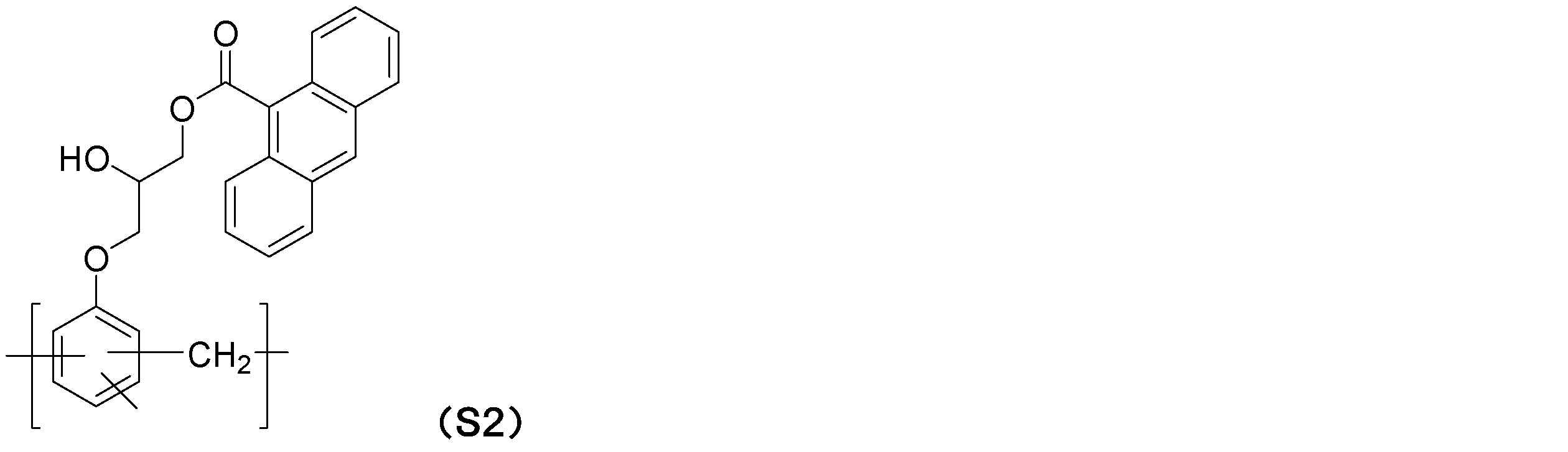
<合成例3>
γ―ブチロラクトンメタクリレート6.6g(0.039モル)、ヒドロキシプロピルメタクリレート6.6g(0.046モル)およびベンジルメタクリレート6.8g(0.039モル)、アゾビスイソブチロニトリル0.2gを乳酸エチル80.4gに溶解させた後、フラスコ内を窒素にて置換し、70℃まで昇温し、24時間反応させ式(S3)の樹脂を得た。 <Synthesis Example 3>
6.6 g (0.039 mol) of γ-butyrolactone methacrylate, 6.6 g (0.046 mol) of hydroxypropyl methacrylate and 6.8 g (0.039 mol) of benzyl methacrylate, 0.2 g of azobisisobutyronitrile were added to lactic acid. After dissolving in 80.4 g of ethyl, the inside of the flask was replaced with nitrogen, the temperature was raised to 70° C., and reaction was performed for 24 hours to obtain a resin of formula (S3).

<合成例4>
9-アントリルメチルメタクリレート5.0g(0.018モル)、ヒドロキシプロピルメタクリレート4.8g(0.034モル)、2,2’-アゾビス(イソ酪酸)ジメチル0.2gをプロピレングリコールモノメチルエーテルアセテート40.2gに溶解させた後、フラスコ内を窒素にて置換し70℃まで昇温し、24時間反応させ、式(S4)の樹脂を得た。 <Synthesis Example 4>
5.0 g (0.018 mol) of 9-anthrylmethyl methacrylate, 4.8 g (0.034 mol) of hydroxypropyl methacrylate, and 0.2 g of dimethyl 2,2′-azobis(isobutyrate) were mixed with propylene glycol monomethyl ether acetate 40. After dissolving in .2 g, the inside of the flask was replaced with nitrogen, the temperature was raised to 70° C., and the reaction was carried out for 24 hours to obtain a resin of the formula (S4).

<b.組成物の調製>
<実施例1(組成物1)、実施例2(組成物2)、実施例3(組成物3)>
合成例1、合成例2および合成例4で得た反応生成物の各々を0.24g含む溶液1.2gにプロピレングリコールモノメチルエーテル5.76gを加えた後、孔径0.10μmのポリエチレン製ミクロフィルターを用いて濾過して光硬化性樹脂組成物を調製した。 <b. Preparation of composition>
<Example 1 (composition 1), Example 2 (composition 2), Example 3 (composition 3)>
After adding 5.76 g of propylene glycol monomethyl ether to 1.2 g of a solution containing 0.24 g of each of the reaction products obtained in Synthesis Example 1, Synthesis Example 2 and Synthesis Example 4, a polyethylene microfilter having a pore size of 0.10 μm was prepared. was filtered to prepare a photocurable resin composition.
<比較例1>
合成例3で得た反応生成物0.24gを含む溶液1.2gにプロピレングリコールモノメチルエーテル5.76gを加えた後、孔径0.10μmのポリエチレン製ミクロフィルターを用いて濾過して光硬化性樹脂組成物を調製した。 <Comparative Example 1>
After adding 5.76 g of propylene glycol monomethyl ether to 1.2 g of the solution containing 0.24 g of the reaction product obtained in Synthesis Example 3, the photocurable resin was filtered using a polyethylene microfilter having a pore size of 0.10 μm. A composition was prepared.
<c.フォトレジスト溶剤への溶出試験>
実施例1、実施例2及び比較例1で調製した光硬化性樹脂組成物の各々をスピナーにより、シリコンウェハー上に塗布した。ホットプレート上で80℃1分間焼成し、その後i線アライナー(PLA-501 キヤノン(株))により365nmの波長の光を3J/cm2照射することにより光硬化膜(膜厚0.10μm)を形成した。この光硬化膜をフォトレジストに使用する溶剤、例えばシクロヘキサノンに浸漬した。実施例1及び実施例2の組成物からの光硬化膜が溶剤に不溶であることを確認したが、比較例1の組成物からの光硬化膜は溶剤により溶解した。 <c. Elution test into photoresist solvent>
Each of the photocurable resin compositions prepared in Examples 1, 2 and Comparative Example 1 was applied onto a silicon wafer using a spinner. Bake on a hot plate at 80° C. for 1 minute, and then irradiate light with a wavelength of 365 nm at 3 J/cm 2 using an i-line aligner (PLA-501, Canon Inc.) to form a photocured film (thickness: 0.10 μm). formed. This photocured film was immersed in a solvent used for photoresist, such as cyclohexanone. It was confirmed that the photocured films from the compositions of Examples 1 and 2 were insoluble in the solvent, but the photocured film from the composition of Comparative Example 1 was soluble in the solvent.
<d.光学パラメーター測定>
実施例1、実施例2及び比較例1で調製した光硬化性樹脂組成物の各々をスピナーにより、シリコンウェハー上に塗布した。ホットプレート上で80℃1分間焼成し、その後i線アライナー(PLA-501 キヤノン(株))により、365nmの波長の光を0.3J/cm2及び3J/cm2の各強度で照射することにより光硬化膜(膜厚0.10μm)を形成した。そして、分光エリプソメーターを用い、これらの光硬化膜の波長248nmでの屈折率(n値)及び減衰係数(k値)を測定した。結果を以下に示す。(n/kの順での表記) <d. Optical parameter measurement>
Each of the photocurable resin compositions prepared in Examples 1, 2 and Comparative Example 1 was applied onto a silicon wafer using a spinner. Bake on a hot plate at 80° C. for 1 minute, and then irradiate light with a wavelength of 365 nm at an intensity of 0.3 J/cm 2 and 3 J/cm 2 using an i-line aligner (PLA-501, Canon Inc.). A photocured film (thickness: 0.10 μm) was formed. Using a spectroscopic ellipsometer, the refractive index (n value) and attenuation coefficient (k value) of these photocured films at a wavelength of 248 nm were measured. The results are shown below. (Notation in the order of n/k)
その結果、実施例1及び実施例2の光硬化膜ではnおよびk値が変化し、構造変化が示唆されたものの、比較例1の光硬化膜ではほとんど値に変化がなかった。
As a result, the n and k values of the photocured films of Examples 1 and 2 changed, suggesting structural changes, but the photocured film of Comparative Example 1 showed almost no change in the values.
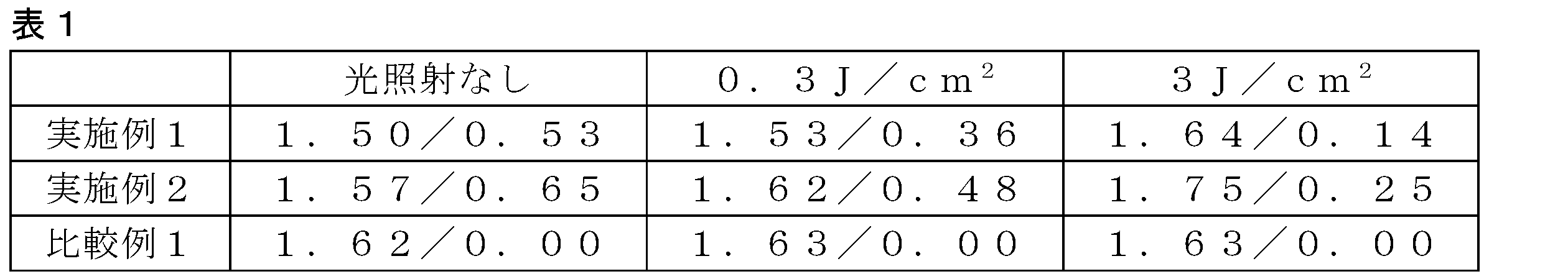
(e.ドライエッチング速度測定)
実施例1、実施例2及び比較例1で調製した光硬化性樹脂組成物の各々をスピナーにより、シリコンウェハー上に塗布した。ホットプレート上で80℃1分間焼成し、その後i線アライナー(PLA-501 キヤノン(株))により、365nmの波長の光を0.3J/cm2及び3J/cm2の各強度で照射することにより光硬化膜(膜厚0.10μm)を形成した。そして、サムコ製エッチャー(RIE―10NR)を用い、ドライエッチングガスとしてCF4を使用した条件下で、これらの光硬化膜のドライエッチング速度(nm/min)を測定した。 (e. Dry etching rate measurement)
Each of the photocurable resin compositions prepared in Examples 1, 2 and Comparative Example 1 was applied onto a silicon wafer using a spinner. Bake on a hot plate at 80° C. for 1 minute, and then irradiate light with a wavelength of 365 nm at an intensity of 0.3 J/cm 2 and 3 J/cm 2 using an i-line aligner (PLA-501, Canon Inc.). A photocured film (thickness: 0.10 μm) was formed. Then, the dry etching rate (nm/min) of these photocured films was measured using an etcher (RIE-10NR) manufactured by Samco under the condition of using CF 4 as a dry etching gas.
実施例1、実施例2及び比較例1の光硬化膜のドライエッチング速度との比較を行った結果、実施例1及び実施例2の光硬化膜ではエッチング速度が光照射により若干低下し、構造変化が示唆されたものの、比較例1の光硬化膜では値に変化がなかった。
As a result of comparison with the dry etching rate of the photocured films of Examples 1, 2, and Comparative Example 1, the etching rate of the photocured films of Examples 1 and 2 slightly decreased due to light irradiation, and the structure Although a change was suggested, the value of the photocured film of Comparative Example 1 did not change.
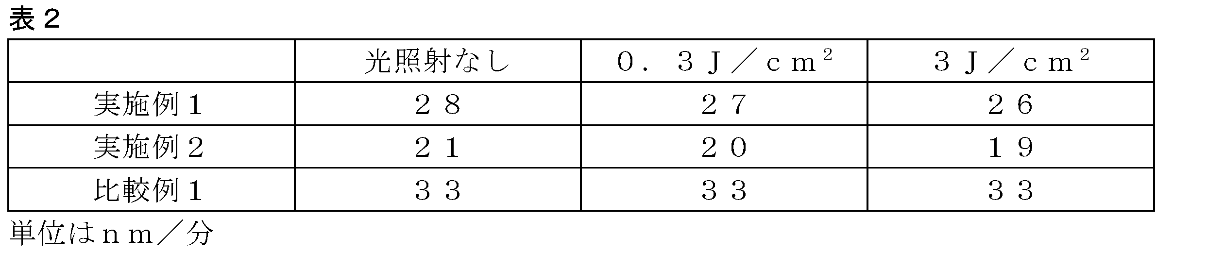
<f.エッジ露光での溶剤耐性試験>
実施例1、実施例2及び比較例1で調製した光硬化性樹脂組成物の各々をスピナーにより、12インチシリコンウェハー上に塗布した。ホットプレート上で80℃1分間焼成し、その後Lithiuspro(東京エレクトロン(株))のWEEによりウェハエッジを50mJ/cm2照射することにより、光硬化膜(膜厚0.30μm)を形成した。この光硬化膜をフォトレジストに使用する溶剤、例えばOK73シンナーに浸漬した。実施例1及び実施例2の光硬化膜が溶剤に不溶であることを確認したが、比較例1の光硬化膜は溶剤により溶解した。 <f. Solvent resistance test in edge exposure>
Each of the photocurable resin compositions prepared in Examples 1, 2 and Comparative Example 1 was applied onto a 12-inch silicon wafer using a spinner. After baking on a hot plate at 80° C. for 1 minute, the wafer edge was irradiated with 50 mJ/cm 2 of WEE from Lithiuspro (Tokyo Electron Ltd.) to form a photocured film (thickness: 0.30 μm). This photocured film was immersed in a solvent used for photoresist, eg, OK73 thinner. It was confirmed that the photocured films of Examples 1 and 2 were insoluble in the solvent, but the photocured film of Comparative Example 1 was dissolved by the solvent.
本発明によれば、半導体製造におけるリソグラフィープロセスにおいて有用な、特に半導体製造用ウエハ端部保護膜を形成するために有用な光硬化性樹脂組成物を提供することができる。
また、当該組成物の光硬化膜、特に半導体製造用ウエハ端部保護膜、当該光硬化膜を有する半導体製造用ウエハ、並びに光硬化性樹脂組成物を利用した積層基板、及び半導体装置の製造方法を提供することができる。 INDUSTRIAL APPLICABILITY According to the present invention, it is possible to provide a photocurable resin composition that is useful in lithography processes in semiconductor manufacturing, and particularly useful for forming wafer edge protection films for semiconductor manufacturing.
In addition, a photocured film of the composition, particularly a semiconductor manufacturing wafer edge protection film, a semiconductor manufacturing wafer having the photocured film, a laminated substrate using the photocurable resin composition, and a method for manufacturing a semiconductor device can be provided.
また、当該組成物の光硬化膜、特に半導体製造用ウエハ端部保護膜、当該光硬化膜を有する半導体製造用ウエハ、並びに光硬化性樹脂組成物を利用した積層基板、及び半導体装置の製造方法を提供することができる。 INDUSTRIAL APPLICABILITY According to the present invention, it is possible to provide a photocurable resin composition that is useful in lithography processes in semiconductor manufacturing, and particularly useful for forming wafer edge protection films for semiconductor manufacturing.
In addition, a photocured film of the composition, particularly a semiconductor manufacturing wafer edge protection film, a semiconductor manufacturing wafer having the photocured film, a laminated substrate using the photocurable resin composition, and a method for manufacturing a semiconductor device can be provided.
Claims (16)
- 多環芳香族炭化水素基を含有するポリマー及び/又は化合物、並びに溶剤を含む、光硬化性樹脂組成物。 A photocurable resin composition containing a polymer and/or compound containing a polycyclic aromatic hydrocarbon group and a solvent.
- 前記多環芳香族炭化水素基が、ナフタレン、アントラセン、フェナントレン及びピレンからなる群より選ばれる少なくとも1種に由来する、請求項1に記載の光硬化性樹脂組成物。 The photocurable resin composition according to claim 1, wherein the polycyclic aromatic hydrocarbon group is derived from at least one selected from the group consisting of naphthalene, anthracene, phenanthrene and pyrene.
- 前記ポリマーが、それぞれ多環芳香族炭化水素基を含有するポリビニルアルコール、ポリアクリルアミド、(メタ)アクリル系樹脂、ポリアミド酸、ポリヒドロキシスチレン、ポリヒドロキシスチレン誘導体、ポリメタクリレートとマレイン酸無水物との共重合体、エポキシ樹脂、フェノール樹脂、ノボラック樹脂、ポリイミド、セルロース、セルロース誘導体、スターチ、キチン、キトサン、ゼラチン、ゼイン、糖骨格高分子化合物、ポリアミド、ポリエチレンテレフタレート、ポリカーボネート、ポリウレタン及びポリシロキサンからなる群より選ばれる少なくとも1種である、請求項1に記載の光硬化性樹脂組成物。 The polymer is polyvinyl alcohol, polyacrylamide, (meth)acrylic resin, polyamic acid, polyhydroxystyrene, polyhydroxystyrene derivative, polymethacrylate and maleic anhydride each containing a polycyclic aromatic hydrocarbon group. polymer, epoxy resin, phenolic resin, novolak resin, polyimide, cellulose, cellulose derivative, starch, chitin, chitosan, gelatin, zein, sugar skeleton polymer compound, polyamide, polyethylene terephthalate, polycarbonate, polyurethane and polysiloxane The photocurable resin composition according to claim 1, which is at least one selected.
- 前記化合物が、複素環構造を更に含む、請求項1に記載の光硬化性樹脂組成物。 The photocurable resin composition according to claim 1, wherein the compound further contains a heterocyclic structure.
- 170~800nmの波長の光で硬化する、請求項1に記載の光硬化性樹脂組成物。 The photocurable resin composition according to claim 1, which is cured with light having a wavelength of 170 to 800 nm.
- 半導体製造用ウエハ端部保護膜を形成するための、請求項1に記載の光硬化性樹脂組成物。 The photocurable resin composition according to claim 1, for forming a wafer edge protective film for semiconductor manufacturing.
- 25℃において100cps以下の粘度を有する、請求項6に記載の光硬化性樹脂組成物。 The photocurable resin composition according to claim 6, which has a viscosity of 100 cps or less at 25°C.
- 請求項1~7何れか1項に記載の光硬化性樹脂組成物からなる塗布膜の光硬化膜。 A photocured film of a coating film made of the photocurable resin composition according to any one of claims 1 to 7.
- 請求項6又は7に記載の光硬化性樹脂組成物からなる塗布膜の光硬化物である半導体製造用ウエハ端部保護膜。 A wafer edge protective film for semiconductor manufacturing, which is a photocured product of a coating film made of the photocurable resin composition according to claim 6 or 7.
- 1nm~10μmの厚みを有する、請求項9に記載の半導体製造用ウエハ端部保護膜。 The wafer edge protection film for semiconductor manufacturing according to claim 9, which has a thickness of 1 nm to 10 µm.
- ウエハ端部の金属汚染を防止するための、請求項9に記載の半導体製造用ウエハ端部保護膜。 The wafer edge protection film for semiconductor manufacturing according to claim 9, for preventing metal contamination at the edge of the wafer.
- 半導体製造用ウエハの端部に、請求項9に記載の半導体製造用ウエハ端部保護膜を有する、半導体製造用ウエハ。 A semiconductor manufacturing wafer having the semiconductor manufacturing wafer edge protection film according to claim 9 on the edge of the semiconductor manufacturing wafer.
- 半導体製造用ウエハ端部保護膜を形成するための、請求項1~7何れか1項に記載の光硬化性樹脂組成物の使用。 Use of the photocurable resin composition according to any one of claims 1 to 7 for forming a wafer edge protection film for semiconductor manufacturing.
- 基板上に、請求項1~7何れか1項に記載の光硬化性樹脂組成物を塗布する工程、及び塗布された組成物を露光する工程を含む、積層基板の製造方法。 A method for producing a laminated substrate, comprising a step of applying the photocurable resin composition according to any one of claims 1 to 7 onto a substrate, and a step of exposing the applied composition.
- 前記基板が、段差を有する、請求項14に記載の積層基板の製造方法。 The method for manufacturing a laminated substrate according to claim 14, wherein the substrate has steps.
- 基板上に、請求項1~7何れか1項に記載の光硬化性樹脂組成物を塗布する工程、及び塗布された組成物を露光する工程を含む、半導体装置の製造方法。 A method for manufacturing a semiconductor device, comprising a step of applying the photocurable resin composition according to any one of claims 1 to 7 on a substrate, and a step of exposing the applied composition.
Applications Claiming Priority (2)
| Application Number | Priority Date | Filing Date | Title |
|---|---|---|---|
| JP2021-185496 | 2021-11-15 | ||
| JP2021185496 | 2021-11-15 |
Publications (1)
| Publication Number | Publication Date |
|---|---|
| WO2023085414A1 true WO2023085414A1 (en) | 2023-05-19 |
Family
ID=86335858
Family Applications (1)
| Application Number | Title | Priority Date | Filing Date |
|---|---|---|---|
| PCT/JP2022/042164 WO2023085414A1 (en) | 2021-11-15 | 2022-11-14 | Polycyclic aromatic hydrocarbon-based photo-curable resin composition |
Country Status (2)
| Country | Link |
|---|---|
| TW (1) | TW202337929A (en) |
| WO (1) | WO2023085414A1 (en) |
Citations (4)
| Publication number | Priority date | Publication date | Assignee | Title |
|---|---|---|---|---|
| JPS57177139A (en) * | 1981-04-02 | 1982-10-30 | Ciba Geigy Ag | Method of forming picture |
| JPH10186647A (en) * | 1996-10-07 | 1998-07-14 | Shipley Co Llc | Colored photoresist, its method and industrial product by using the same |
| US20150357571A1 (en) * | 2012-11-30 | 2015-12-10 | Lg Display Co., Ltd. | Photoresist Employing Photodimerization Chemistry and Method for Manufacturing Organic Light Emitting Diode Display Using the Same |
| WO2019054420A1 (en) * | 2017-09-13 | 2019-03-21 | 日産化学株式会社 | Stepped substrate coating composition containing compound having curable functional group |
-
2022
- 2022-11-14 TW TW111143337A patent/TW202337929A/en unknown
- 2022-11-14 WO PCT/JP2022/042164 patent/WO2023085414A1/en active Application Filing
Patent Citations (4)
| Publication number | Priority date | Publication date | Assignee | Title |
|---|---|---|---|---|
| JPS57177139A (en) * | 1981-04-02 | 1982-10-30 | Ciba Geigy Ag | Method of forming picture |
| JPH10186647A (en) * | 1996-10-07 | 1998-07-14 | Shipley Co Llc | Colored photoresist, its method and industrial product by using the same |
| US20150357571A1 (en) * | 2012-11-30 | 2015-12-10 | Lg Display Co., Ltd. | Photoresist Employing Photodimerization Chemistry and Method for Manufacturing Organic Light Emitting Diode Display Using the Same |
| WO2019054420A1 (en) * | 2017-09-13 | 2019-03-21 | 日産化学株式会社 | Stepped substrate coating composition containing compound having curable functional group |
Also Published As
| Publication number | Publication date |
|---|---|
| TW202337929A (en) | 2023-10-01 |
Similar Documents
| Publication | Publication Date | Title |
|---|---|---|
| TWI642698B (en) | Stable metal compounds as hardmasks and filling materials, their compositions and methods of use | |
| JP6810696B2 (en) | Hardmask composition and method for forming fine patterns on semiconductor substrates | |
| JP6342998B2 (en) | Spin-on compositions of soluble metal oxide carboxylates and methods for their use | |
| US9384977B2 (en) | Method of manufacturing semiconductor device using organic underlayer film forming composition for solvent development lithography process | |
| JP6430954B2 (en) | Stable metal compound, composition thereof, and method of use thereof | |
| JP5708938B2 (en) | Photosensitive resist underlayer film forming composition and resist pattern forming method | |
| CN110780536B (en) | Semiconductor resist composition and method and system for forming pattern using the same | |
| KR20120022889A (en) | Composition for forming resist underlayer film for euv lithography | |
| WO2006126406A1 (en) | Polysilane compound-containing lower layer film forming composition for lithography | |
| CN104914672B (en) | Bottom anti-reflection composition based on molecular glass containing polyhydroxy structure and application thereof | |
| JP6311702B2 (en) | Inorganic film forming composition for multilayer resist process and pattern forming method | |
| JP4221610B2 (en) | Lithographic gap fill material forming composition containing acrylic polymer | |
| JP6195078B2 (en) | Silicon-containing resist underlayer film forming composition having sulfone structure and amine structure | |
| KR20160126970A (en) | Composition for forming upper-layer resist film, and method for manufacturing semiconductor device using said composition | |
| JP2010285403A (en) | Crosslinking agent and crosslinking agent-containing composition for forming lower layer of resist film | |
| WO2012081619A1 (en) | Composition for forming resist underlayer film and method for forming resist pattern using same | |
| WO2014046055A1 (en) | Silicon-containing resist underlayer film-forming composition which contains cyclic organic group having heteroatom | |
| TWI776174B (en) | Antireflective coating composition including photoacid generator, coated substrate and method of forming pattern | |
| WO2023085414A1 (en) | Polycyclic aromatic hydrocarbon-based photo-curable resin composition | |
| JP2004205900A (en) | Composition for formation of antireflection film containing polymer containing phosphorus-based organic group | |
| JP5534205B2 (en) | Photosensitive resist underlayer film forming composition and resist pattern forming method | |
| WO2023033094A1 (en) | Wafer edge protective-film-forming composition for semiconductor manufacturing | |
| WO2023162968A1 (en) | Photocurable resin composition containing self-crosslinking polymer | |
| WO2015012177A1 (en) | Method for forming pattern | |
| WO2023171733A1 (en) | Wafer edge protective film-forming composition for semiconductor manufacturing |
Legal Events
| Date | Code | Title | Description |
|---|---|---|---|
| 121 | Ep: the epo has been informed by wipo that ep was designated in this application |
Ref document number: 22892912 Country of ref document: EP Kind code of ref document: A1 |
|
| WWE | Wipo information: entry into national phase |
Ref document number: 2023559937 Country of ref document: JP |