WO2020008299A1 - Display device and electronic device - Google Patents
Display device and electronic device Download PDFInfo
- Publication number
- WO2020008299A1 WO2020008299A1 PCT/IB2019/055325 IB2019055325W WO2020008299A1 WO 2020008299 A1 WO2020008299 A1 WO 2020008299A1 IB 2019055325 W IB2019055325 W IB 2019055325W WO 2020008299 A1 WO2020008299 A1 WO 2020008299A1
- Authority
- WO
- WIPO (PCT)
- Prior art keywords
- transistor
- electrode
- circuit
- display device
- light
- Prior art date
Links
- 239000003990 capacitor Substances 0.000 claims description 114
- 239000004973 liquid crystal related substance Substances 0.000 claims description 98
- 230000015572 biosynthetic process Effects 0.000 claims description 16
- 229910052738 indium Inorganic materials 0.000 claims description 9
- 229910044991 metal oxide Inorganic materials 0.000 claims description 9
- 150000004706 metal oxides Chemical class 0.000 claims description 9
- 229910052733 gallium Inorganic materials 0.000 claims description 8
- 229910052719 titanium Inorganic materials 0.000 claims description 8
- 229910052782 aluminium Inorganic materials 0.000 claims description 7
- 229910052735 hafnium Inorganic materials 0.000 claims description 6
- 229910052725 zinc Inorganic materials 0.000 claims description 6
- 229910052684 Cerium Inorganic materials 0.000 claims description 5
- 229910052779 Neodymium Inorganic materials 0.000 claims description 5
- 229910052727 yttrium Inorganic materials 0.000 claims description 5
- 229910052746 lanthanum Inorganic materials 0.000 claims description 4
- -1 or Zr. Inorganic materials 0.000 claims description 3
- 229910052718 tin Inorganic materials 0.000 claims description 3
- 239000010410 layer Substances 0.000 description 240
- 239000004065 semiconductor Substances 0.000 description 123
- 230000006870 function Effects 0.000 description 62
- 239000000758 substrate Substances 0.000 description 49
- 238000000034 method Methods 0.000 description 41
- 239000000463 material Substances 0.000 description 35
- 239000011701 zinc Substances 0.000 description 33
- 239000010408 film Substances 0.000 description 30
- 238000010586 diagram Methods 0.000 description 22
- 230000001965 increasing effect Effects 0.000 description 22
- 229920005989 resin Polymers 0.000 description 22
- 239000011347 resin Substances 0.000 description 22
- 229910052760 oxygen Inorganic materials 0.000 description 16
- 238000004088 simulation Methods 0.000 description 16
- 229910052751 metal Inorganic materials 0.000 description 15
- 238000000149 argon plasma sintering Methods 0.000 description 14
- QVGXLLKOCUKJST-UHFFFAOYSA-N atomic oxygen Chemical compound [O] QVGXLLKOCUKJST-UHFFFAOYSA-N 0.000 description 14
- 239000002131 composite material Substances 0.000 description 14
- 230000005684 electric field Effects 0.000 description 14
- 239000001301 oxygen Substances 0.000 description 14
- 239000013078 crystal Substances 0.000 description 13
- 125000004429 atom Chemical group 0.000 description 12
- 239000012535 impurity Substances 0.000 description 12
- 230000001976 improved effect Effects 0.000 description 11
- 239000002184 metal Substances 0.000 description 11
- 238000009792 diffusion process Methods 0.000 description 10
- 239000000203 mixture Substances 0.000 description 10
- 230000003287 optical effect Effects 0.000 description 10
- IJGRMHOSHXDMSA-UHFFFAOYSA-N Atomic nitrogen Chemical compound N#N IJGRMHOSHXDMSA-UHFFFAOYSA-N 0.000 description 9
- 239000001257 hydrogen Substances 0.000 description 9
- 229910052739 hydrogen Inorganic materials 0.000 description 9
- XLOMVQKBTHCTTD-UHFFFAOYSA-N Zinc monoxide Chemical compound [Zn]=O XLOMVQKBTHCTTD-UHFFFAOYSA-N 0.000 description 8
- 150000001875 compounds Chemical class 0.000 description 8
- 230000008878 coupling Effects 0.000 description 8
- 238000010168 coupling process Methods 0.000 description 8
- 238000005859 coupling reaction Methods 0.000 description 8
- 230000007547 defect Effects 0.000 description 8
- 238000004519 manufacturing process Methods 0.000 description 8
- 239000000565 sealant Substances 0.000 description 8
- 239000010936 titanium Substances 0.000 description 8
- UFHFLCQGNIYNRP-UHFFFAOYSA-N Hydrogen Chemical compound [H][H] UFHFLCQGNIYNRP-UHFFFAOYSA-N 0.000 description 7
- PXHVJJICTQNCMI-UHFFFAOYSA-N Nickel Chemical compound [Ni] PXHVJJICTQNCMI-UHFFFAOYSA-N 0.000 description 7
- 238000004040 coloring Methods 0.000 description 7
- 230000003071 parasitic effect Effects 0.000 description 7
- 239000000126 substance Substances 0.000 description 7
- RTAQQCXQSZGOHL-UHFFFAOYSA-N Titanium Chemical compound [Ti] RTAQQCXQSZGOHL-UHFFFAOYSA-N 0.000 description 6
- 238000003860 storage Methods 0.000 description 6
- XUIMIQQOPSSXEZ-UHFFFAOYSA-N Silicon Chemical compound [Si] XUIMIQQOPSSXEZ-UHFFFAOYSA-N 0.000 description 5
- XAGFODPZIPBFFR-UHFFFAOYSA-N aluminium Chemical compound [Al] XAGFODPZIPBFFR-UHFFFAOYSA-N 0.000 description 5
- 239000003086 colorant Substances 0.000 description 5
- 230000002349 favourable effect Effects 0.000 description 5
- 230000005669 field effect Effects 0.000 description 5
- APFVFJFRJDLVQX-UHFFFAOYSA-N indium atom Chemical compound [In] APFVFJFRJDLVQX-UHFFFAOYSA-N 0.000 description 5
- 230000007246 mechanism Effects 0.000 description 5
- 229910052710 silicon Inorganic materials 0.000 description 5
- 239000010703 silicon Substances 0.000 description 5
- 125000006850 spacer group Chemical group 0.000 description 5
- XKRFYHLGVUSROY-UHFFFAOYSA-N Argon Chemical compound [Ar] XKRFYHLGVUSROY-UHFFFAOYSA-N 0.000 description 4
- GYHNNYVSQQEPJS-UHFFFAOYSA-N Gallium Chemical compound [Ga] GYHNNYVSQQEPJS-UHFFFAOYSA-N 0.000 description 4
- XEEYBQQBJWHFJM-UHFFFAOYSA-N Iron Chemical compound [Fe] XEEYBQQBJWHFJM-UHFFFAOYSA-N 0.000 description 4
- 239000004983 Polymer Dispersed Liquid Crystal Substances 0.000 description 4
- 239000000969 carrier Substances 0.000 description 4
- 230000008859 change Effects 0.000 description 4
- 239000010949 copper Substances 0.000 description 4
- 238000012937 correction Methods 0.000 description 4
- 238000000295 emission spectrum Methods 0.000 description 4
- 239000000945 filler Substances 0.000 description 4
- 239000011521 glass Substances 0.000 description 4
- VBJZVLUMGGDVMO-UHFFFAOYSA-N hafnium atom Chemical compound [Hf] VBJZVLUMGGDVMO-UHFFFAOYSA-N 0.000 description 4
- 239000002105 nanoparticle Substances 0.000 description 4
- 229910052757 nitrogen Inorganic materials 0.000 description 4
- 238000005192 partition Methods 0.000 description 4
- 239000011241 protective layer Substances 0.000 description 4
- 238000001004 secondary ion mass spectrometry Methods 0.000 description 4
- WFKWXMTUELFFGS-UHFFFAOYSA-N tungsten Chemical compound [W] WFKWXMTUELFFGS-UHFFFAOYSA-N 0.000 description 4
- 229910052721 tungsten Inorganic materials 0.000 description 4
- 239000010937 tungsten Substances 0.000 description 4
- 239000011787 zinc oxide Substances 0.000 description 4
- 229910052726 zirconium Inorganic materials 0.000 description 4
- UWCWUCKPEYNDNV-LBPRGKRZSA-N 2,6-dimethyl-n-[[(2s)-pyrrolidin-2-yl]methyl]aniline Chemical compound CC1=CC=CC(C)=C1NC[C@H]1NCCC1 UWCWUCKPEYNDNV-LBPRGKRZSA-N 0.000 description 3
- OKTJSMMVPCPJKN-UHFFFAOYSA-N Carbon Chemical compound [C] OKTJSMMVPCPJKN-UHFFFAOYSA-N 0.000 description 3
- RYGMFSIKBFXOCR-UHFFFAOYSA-N Copper Chemical compound [Cu] RYGMFSIKBFXOCR-UHFFFAOYSA-N 0.000 description 3
- MYMOFIZGZYHOMD-UHFFFAOYSA-N Dioxygen Chemical compound O=O MYMOFIZGZYHOMD-UHFFFAOYSA-N 0.000 description 3
- ZOKXTWBITQBERF-UHFFFAOYSA-N Molybdenum Chemical compound [Mo] ZOKXTWBITQBERF-UHFFFAOYSA-N 0.000 description 3
- 238000002441 X-ray diffraction Methods 0.000 description 3
- QCWXUUIWCKQGHC-UHFFFAOYSA-N Zirconium Chemical compound [Zr] QCWXUUIWCKQGHC-UHFFFAOYSA-N 0.000 description 3
- 238000013459 approach Methods 0.000 description 3
- 230000005540 biological transmission Effects 0.000 description 3
- 229910052799 carbon Inorganic materials 0.000 description 3
- ZMIGMASIKSOYAM-UHFFFAOYSA-N cerium Chemical compound [Ce][Ce][Ce][Ce][Ce][Ce][Ce][Ce][Ce][Ce][Ce][Ce][Ce][Ce][Ce][Ce][Ce][Ce][Ce][Ce][Ce][Ce][Ce][Ce][Ce][Ce][Ce][Ce][Ce][Ce][Ce][Ce][Ce][Ce][Ce][Ce][Ce][Ce] ZMIGMASIKSOYAM-UHFFFAOYSA-N 0.000 description 3
- 239000004020 conductor Substances 0.000 description 3
- 229910052802 copper Inorganic materials 0.000 description 3
- 238000001514 detection method Methods 0.000 description 3
- 229910001882 dioxygen Inorganic materials 0.000 description 3
- 230000000694 effects Effects 0.000 description 3
- 238000010894 electron beam technology Methods 0.000 description 3
- 238000002149 energy-dispersive X-ray emission spectroscopy Methods 0.000 description 3
- 230000001747 exhibiting effect Effects 0.000 description 3
- 238000007667 floating Methods 0.000 description 3
- 229910052732 germanium Inorganic materials 0.000 description 3
- GNPVGFCGXDBREM-UHFFFAOYSA-N germanium atom Chemical compound [Ge] GNPVGFCGXDBREM-UHFFFAOYSA-N 0.000 description 3
- 229910003437 indium oxide Inorganic materials 0.000 description 3
- PJXISJQVUVHSOJ-UHFFFAOYSA-N indium(iii) oxide Chemical compound [O-2].[O-2].[O-2].[In+3].[In+3] PJXISJQVUVHSOJ-UHFFFAOYSA-N 0.000 description 3
- 229910010272 inorganic material Inorganic materials 0.000 description 3
- FZLIPJUXYLNCLC-UHFFFAOYSA-N lanthanum atom Chemical compound [La] FZLIPJUXYLNCLC-UHFFFAOYSA-N 0.000 description 3
- 229910052750 molybdenum Inorganic materials 0.000 description 3
- 239000011733 molybdenum Substances 0.000 description 3
- QEFYFXOXNSNQGX-UHFFFAOYSA-N neodymium atom Chemical compound [Nd] QEFYFXOXNSNQGX-UHFFFAOYSA-N 0.000 description 3
- 229910052759 nickel Inorganic materials 0.000 description 3
- 150000002894 organic compounds Chemical class 0.000 description 3
- BASFCYQUMIYNBI-UHFFFAOYSA-N platinum Chemical compound [Pt] BASFCYQUMIYNBI-UHFFFAOYSA-N 0.000 description 3
- 229920000642 polymer Polymers 0.000 description 3
- 238000005477 sputtering target Methods 0.000 description 3
- 229910052715 tantalum Inorganic materials 0.000 description 3
- GUVRBAGPIYLISA-UHFFFAOYSA-N tantalum atom Chemical compound [Ta] GUVRBAGPIYLISA-UHFFFAOYSA-N 0.000 description 3
- 239000010409 thin film Substances 0.000 description 3
- 238000002834 transmittance Methods 0.000 description 3
- VWQVUPCCIRVNHF-UHFFFAOYSA-N yttrium atom Chemical compound [Y] VWQVUPCCIRVNHF-UHFFFAOYSA-N 0.000 description 3
- YVTHLONGBIQYBO-UHFFFAOYSA-N zinc indium(3+) oxygen(2-) Chemical compound [O--].[Zn++].[In+3] YVTHLONGBIQYBO-UHFFFAOYSA-N 0.000 description 3
- VUFNLQXQSDUXKB-DOFZRALJSA-N 2-[4-[4-[bis(2-chloroethyl)amino]phenyl]butanoyloxy]ethyl (5z,8z,11z,14z)-icosa-5,8,11,14-tetraenoate Chemical group CCCCC\C=C/C\C=C/C\C=C/C\C=C/CCCC(=O)OCCOC(=O)CCCC1=CC=C(N(CCCl)CCCl)C=C1 VUFNLQXQSDUXKB-DOFZRALJSA-N 0.000 description 2
- PAYRUJLWNCNPSJ-UHFFFAOYSA-N Aniline Chemical compound NC1=CC=CC=C1 PAYRUJLWNCNPSJ-UHFFFAOYSA-N 0.000 description 2
- ZOXJGFHDIHLPTG-UHFFFAOYSA-N Boron Chemical compound [B] ZOXJGFHDIHLPTG-UHFFFAOYSA-N 0.000 description 2
- CURLTUGMZLYLDI-UHFFFAOYSA-N Carbon dioxide Chemical compound O=C=O CURLTUGMZLYLDI-UHFFFAOYSA-N 0.000 description 2
- 206010052128 Glare Diseases 0.000 description 2
- FYYHWMGAXLPEAU-UHFFFAOYSA-N Magnesium Chemical compound [Mg] FYYHWMGAXLPEAU-UHFFFAOYSA-N 0.000 description 2
- KAESVJOAVNADME-UHFFFAOYSA-N Pyrrole Chemical compound C=1C=CNC=1 KAESVJOAVNADME-UHFFFAOYSA-N 0.000 description 2
- 229910052581 Si3N4 Inorganic materials 0.000 description 2
- YTPLMLYBLZKORZ-UHFFFAOYSA-N Thiophene Chemical compound C=1C=CSC=1 YTPLMLYBLZKORZ-UHFFFAOYSA-N 0.000 description 2
- GWEVSGVZZGPLCZ-UHFFFAOYSA-N Titan oxide Chemical compound O=[Ti]=O GWEVSGVZZGPLCZ-UHFFFAOYSA-N 0.000 description 2
- HCHKCACWOHOZIP-UHFFFAOYSA-N Zinc Chemical compound [Zn] HCHKCACWOHOZIP-UHFFFAOYSA-N 0.000 description 2
- 230000009471 action Effects 0.000 description 2
- 229910052783 alkali metal Inorganic materials 0.000 description 2
- 150000001340 alkali metals Chemical class 0.000 description 2
- 229910052784 alkaline earth metal Inorganic materials 0.000 description 2
- 150000001342 alkaline earth metals Chemical class 0.000 description 2
- 229910052786 argon Inorganic materials 0.000 description 2
- 229910052790 beryllium Inorganic materials 0.000 description 2
- ATBAMAFKBVZNFJ-UHFFFAOYSA-N beryllium atom Chemical compound [Be] ATBAMAFKBVZNFJ-UHFFFAOYSA-N 0.000 description 2
- 229910052796 boron Inorganic materials 0.000 description 2
- DQXBYHZEEUGOBF-UHFFFAOYSA-N but-3-enoic acid;ethene Chemical compound C=C.OC(=O)CC=C DQXBYHZEEUGOBF-UHFFFAOYSA-N 0.000 description 2
- 230000015556 catabolic process Effects 0.000 description 2
- 230000003098 cholesteric effect Effects 0.000 description 2
- 239000011651 chromium Substances 0.000 description 2
- 238000000576 coating method Methods 0.000 description 2
- 238000004891 communication Methods 0.000 description 2
- PMHQVHHXPFUNSP-UHFFFAOYSA-M copper(1+);methylsulfanylmethane;bromide Chemical compound Br[Cu].CSC PMHQVHHXPFUNSP-UHFFFAOYSA-M 0.000 description 2
- 239000002274 desiccant Substances 0.000 description 2
- 230000006866 deterioration Effects 0.000 description 2
- 238000009826 distribution Methods 0.000 description 2
- 230000009977 dual effect Effects 0.000 description 2
- 230000005611 electricity Effects 0.000 description 2
- 239000005038 ethylene vinyl acetate Substances 0.000 description 2
- 230000005281 excited state Effects 0.000 description 2
- 239000005262 ferroelectric liquid crystals (FLCs) Substances 0.000 description 2
- 239000007789 gas Substances 0.000 description 2
- 230000005525 hole transport Effects 0.000 description 2
- 238000003384 imaging method Methods 0.000 description 2
- AMGQUBHHOARCQH-UHFFFAOYSA-N indium;oxotin Chemical compound [In].[Sn]=O AMGQUBHHOARCQH-UHFFFAOYSA-N 0.000 description 2
- 239000011261 inert gas Substances 0.000 description 2
- 238000002347 injection Methods 0.000 description 2
- 239000007924 injection Substances 0.000 description 2
- 150000002484 inorganic compounds Chemical class 0.000 description 2
- 239000011810 insulating material Substances 0.000 description 2
- 229910052742 iron Inorganic materials 0.000 description 2
- 229910052749 magnesium Inorganic materials 0.000 description 2
- 239000011777 magnesium Substances 0.000 description 2
- 238000002156 mixing Methods 0.000 description 2
- 239000000178 monomer Substances 0.000 description 2
- 239000002159 nanocrystal Substances 0.000 description 2
- 239000010955 niobium Substances 0.000 description 2
- QGLKJKCYBOYXKC-UHFFFAOYSA-N nonaoxidotritungsten Chemical compound O=[W]1(=O)O[W](=O)(=O)O[W](=O)(=O)O1 QGLKJKCYBOYXKC-UHFFFAOYSA-N 0.000 description 2
- 239000002245 particle Substances 0.000 description 2
- 230000002093 peripheral effect Effects 0.000 description 2
- 229920001200 poly(ethylene-vinyl acetate) Polymers 0.000 description 2
- 229920002037 poly(vinyl butyral) polymer Polymers 0.000 description 2
- 229920000915 polyvinyl chloride Polymers 0.000 description 2
- 239000004800 polyvinyl chloride Substances 0.000 description 2
- 230000008569 process Effects 0.000 description 2
- 239000002096 quantum dot Substances 0.000 description 2
- 230000006798 recombination Effects 0.000 description 2
- 238000005215 recombination Methods 0.000 description 2
- 230000004044 response Effects 0.000 description 2
- HQVNEWCFYHHQES-UHFFFAOYSA-N silicon nitride Chemical compound N12[Si]34N5[Si]62N3[Si]51N64 HQVNEWCFYHHQES-UHFFFAOYSA-N 0.000 description 2
- 239000002356 single layer Substances 0.000 description 2
- 238000004544 sputter deposition Methods 0.000 description 2
- 230000003068 static effect Effects 0.000 description 2
- 229920001187 thermosetting polymer Polymers 0.000 description 2
- OGIDPMRJRNCKJF-UHFFFAOYSA-N titanium oxide Inorganic materials [Ti]=O OGIDPMRJRNCKJF-UHFFFAOYSA-N 0.000 description 2
- 230000007704 transition Effects 0.000 description 2
- 229910001930 tungsten oxide Inorganic materials 0.000 description 2
- 229910052720 vanadium Inorganic materials 0.000 description 2
- GPPXJZIENCGNKB-UHFFFAOYSA-N vanadium Chemical compound [V]#[V] GPPXJZIENCGNKB-UHFFFAOYSA-N 0.000 description 2
- NIXOWILDQLNWCW-UHFFFAOYSA-M Acrylate Chemical compound [O-]C(=O)C=C NIXOWILDQLNWCW-UHFFFAOYSA-M 0.000 description 1
- 239000004925 Acrylic resin Substances 0.000 description 1
- 229920000178 Acrylic resin Polymers 0.000 description 1
- 239000004986 Cholesteric liquid crystals (ChLC) Substances 0.000 description 1
- VYZAMTAEIAYCRO-UHFFFAOYSA-N Chromium Chemical compound [Cr] VYZAMTAEIAYCRO-UHFFFAOYSA-N 0.000 description 1
- 239000005264 High molar mass liquid crystal Substances 0.000 description 1
- 206010021143 Hypoxia Diseases 0.000 description 1
- 241001544487 Macromiidae Species 0.000 description 1
- CERQOIWHTDAKMF-UHFFFAOYSA-M Methacrylate Chemical compound CC(=C)C([O-])=O CERQOIWHTDAKMF-UHFFFAOYSA-M 0.000 description 1
- 239000004988 Nematic liquid crystal Substances 0.000 description 1
- 239000004642 Polyimide Substances 0.000 description 1
- VYPSYNLAJGMNEJ-UHFFFAOYSA-N Silicium dioxide Chemical compound O=[Si]=O VYPSYNLAJGMNEJ-UHFFFAOYSA-N 0.000 description 1
- BQCADISMDOOEFD-UHFFFAOYSA-N Silver Chemical compound [Ag] BQCADISMDOOEFD-UHFFFAOYSA-N 0.000 description 1
- 239000004990 Smectic liquid crystal Substances 0.000 description 1
- 239000004974 Thermotropic liquid crystal Substances 0.000 description 1
- ATJFFYVFTNAWJD-UHFFFAOYSA-N Tin Chemical compound [Sn] ATJFFYVFTNAWJD-UHFFFAOYSA-N 0.000 description 1
- 239000000654 additive Substances 0.000 description 1
- 230000000996 additive effect Effects 0.000 description 1
- 229910045601 alloy Inorganic materials 0.000 description 1
- 239000000956 alloy Substances 0.000 description 1
- 229910021417 amorphous silicon Inorganic materials 0.000 description 1
- 230000002238 attenuated effect Effects 0.000 description 1
- 230000008901 benefit Effects 0.000 description 1
- 239000011230 binding agent Substances 0.000 description 1
- 239000006229 carbon black Substances 0.000 description 1
- 229910002092 carbon dioxide Inorganic materials 0.000 description 1
- 239000001569 carbon dioxide Substances 0.000 description 1
- 229910052800 carbon group element Inorganic materials 0.000 description 1
- 230000001413 cellular effect Effects 0.000 description 1
- 238000006243 chemical reaction Methods 0.000 description 1
- 229910052804 chromium Inorganic materials 0.000 description 1
- 239000011248 coating agent Substances 0.000 description 1
- 229910017052 cobalt Inorganic materials 0.000 description 1
- 239000010941 cobalt Substances 0.000 description 1
- GUTLYIVDDKVIGB-UHFFFAOYSA-N cobalt atom Chemical compound [Co] GUTLYIVDDKVIGB-UHFFFAOYSA-N 0.000 description 1
- 229920001940 conductive polymer Polymers 0.000 description 1
- 239000000470 constituent Substances 0.000 description 1
- 229920001577 copolymer Polymers 0.000 description 1
- 229910021419 crystalline silicon Inorganic materials 0.000 description 1
- 238000007872 degassing Methods 0.000 description 1
- 238000000151 deposition Methods 0.000 description 1
- 230000008021 deposition Effects 0.000 description 1
- 125000004386 diacrylate group Chemical group 0.000 description 1
- 229910003460 diamond Inorganic materials 0.000 description 1
- 239000010432 diamond Substances 0.000 description 1
- AJNVQOSZGJRYEI-UHFFFAOYSA-N digallium;oxygen(2-) Chemical compound [O-2].[O-2].[O-2].[Ga+3].[Ga+3] AJNVQOSZGJRYEI-UHFFFAOYSA-N 0.000 description 1
- 229910001873 dinitrogen Inorganic materials 0.000 description 1
- 238000005401 electroluminescence Methods 0.000 description 1
- 238000002524 electron diffraction data Methods 0.000 description 1
- 238000000724 energy-dispersive X-ray spectrum Methods 0.000 description 1
- 238000005516 engineering process Methods 0.000 description 1
- 239000003822 epoxy resin Substances 0.000 description 1
- 238000005530 etching Methods 0.000 description 1
- 238000001704 evaporation Methods 0.000 description 1
- 230000005284 excitation Effects 0.000 description 1
- 238000000605 extraction Methods 0.000 description 1
- 229910001195 gallium oxide Inorganic materials 0.000 description 1
- 230000004313 glare Effects 0.000 description 1
- 230000005283 ground state Effects 0.000 description 1
- 230000012447 hatching Effects 0.000 description 1
- 150000002431 hydrogen Chemical class 0.000 description 1
- 125000004435 hydrogen atom Chemical group [H]* 0.000 description 1
- 230000001771 impaired effect Effects 0.000 description 1
- 230000001939 inductive effect Effects 0.000 description 1
- 239000011147 inorganic material Substances 0.000 description 1
- 230000001678 irradiating effect Effects 0.000 description 1
- 238000013507 mapping Methods 0.000 description 1
- 239000011159 matrix material Substances 0.000 description 1
- 238000005259 measurement Methods 0.000 description 1
- 238000000691 measurement method Methods 0.000 description 1
- 229910021645 metal ion Inorganic materials 0.000 description 1
- 239000007769 metal material Substances 0.000 description 1
- 229910021424 microcrystalline silicon Inorganic materials 0.000 description 1
- 238000004377 microelectronic Methods 0.000 description 1
- 238000012986 modification Methods 0.000 description 1
- 230000004048 modification Effects 0.000 description 1
- 229910021421 monocrystalline silicon Inorganic materials 0.000 description 1
- 229910052758 niobium Inorganic materials 0.000 description 1
- GUCVJGMIXFAOAE-UHFFFAOYSA-N niobium atom Chemical compound [Nb] GUCVJGMIXFAOAE-UHFFFAOYSA-N 0.000 description 1
- 150000004767 nitrides Chemical class 0.000 description 1
- 239000012788 optical film Substances 0.000 description 1
- TWNQGVIAIRXVLR-UHFFFAOYSA-N oxo(oxoalumanyloxy)alumane Chemical compound O=[Al]O[Al]=O TWNQGVIAIRXVLR-UHFFFAOYSA-N 0.000 description 1
- 239000000049 pigment Substances 0.000 description 1
- 229910052697 platinum Inorganic materials 0.000 description 1
- 229920000767 polyaniline Polymers 0.000 description 1
- 229910021420 polycrystalline silicon Inorganic materials 0.000 description 1
- 229920000647 polyepoxide Polymers 0.000 description 1
- 229920001721 polyimide Polymers 0.000 description 1
- 229920000128 polypyrrole Polymers 0.000 description 1
- 229920005591 polysilicon Polymers 0.000 description 1
- 229920000123 polythiophene Polymers 0.000 description 1
- 238000007639 printing Methods 0.000 description 1
- 230000001681 protective effect Effects 0.000 description 1
- 239000000523 sample Substances 0.000 description 1
- 239000003566 sealing material Substances 0.000 description 1
- VSZWPYCFIRKVQL-UHFFFAOYSA-N selanylidenegallium;selenium Chemical compound [Se].[Se]=[Ga].[Se]=[Ga] VSZWPYCFIRKVQL-UHFFFAOYSA-N 0.000 description 1
- 229910052814 silicon oxide Inorganic materials 0.000 description 1
- 229920002050 silicone resin Polymers 0.000 description 1
- 229910052709 silver Inorganic materials 0.000 description 1
- 239000004332 silver Substances 0.000 description 1
- 239000006104 solid solution Substances 0.000 description 1
- 235000013599 spices Nutrition 0.000 description 1
- 230000008093 supporting effect Effects 0.000 description 1
- 238000010897 surface acoustic wave method Methods 0.000 description 1
- 229930192474 thiophene Natural products 0.000 description 1
- XOLBLPGZBRYERU-UHFFFAOYSA-N tin dioxide Chemical compound O=[Sn]=O XOLBLPGZBRYERU-UHFFFAOYSA-N 0.000 description 1
- 229910001887 tin oxide Inorganic materials 0.000 description 1
- 238000012546 transfer Methods 0.000 description 1
- 238000001771 vacuum deposition Methods 0.000 description 1
- LEONUFNNVUYDNQ-UHFFFAOYSA-N vanadium atom Chemical compound [V] LEONUFNNVUYDNQ-UHFFFAOYSA-N 0.000 description 1
- 230000000007 visual effect Effects 0.000 description 1
- XLYOFNOQVPJJNP-UHFFFAOYSA-N water Substances O XLYOFNOQVPJJNP-UHFFFAOYSA-N 0.000 description 1
Images


Classifications
-
- G—PHYSICS
- G09—EDUCATION; CRYPTOGRAPHY; DISPLAY; ADVERTISING; SEALS
- G09G—ARRANGEMENTS OR CIRCUITS FOR CONTROL OF INDICATING DEVICES USING STATIC MEANS TO PRESENT VARIABLE INFORMATION
- G09G3/00—Control arrangements or circuits, of interest only in connection with visual indicators other than cathode-ray tubes
- G09G3/20—Control arrangements or circuits, of interest only in connection with visual indicators other than cathode-ray tubes for presentation of an assembly of a number of characters, e.g. a page, by composing the assembly by combination of individual elements arranged in a matrix no fixed position being assigned to or needed to be assigned to the individual characters or partial characters
- G09G3/34—Control arrangements or circuits, of interest only in connection with visual indicators other than cathode-ray tubes for presentation of an assembly of a number of characters, e.g. a page, by composing the assembly by combination of individual elements arranged in a matrix no fixed position being assigned to or needed to be assigned to the individual characters or partial characters by control of light from an independent source
- G09G3/36—Control arrangements or circuits, of interest only in connection with visual indicators other than cathode-ray tubes for presentation of an assembly of a number of characters, e.g. a page, by composing the assembly by combination of individual elements arranged in a matrix no fixed position being assigned to or needed to be assigned to the individual characters or partial characters by control of light from an independent source using liquid crystals
-
- G—PHYSICS
- G02—OPTICS
- G02F—OPTICAL DEVICES OR ARRANGEMENTS FOR THE CONTROL OF LIGHT BY MODIFICATION OF THE OPTICAL PROPERTIES OF THE MEDIA OF THE ELEMENTS INVOLVED THEREIN; NON-LINEAR OPTICS; FREQUENCY-CHANGING OF LIGHT; OPTICAL LOGIC ELEMENTS; OPTICAL ANALOGUE/DIGITAL CONVERTERS
- G02F1/00—Devices or arrangements for the control of the intensity, colour, phase, polarisation or direction of light arriving from an independent light source, e.g. switching, gating or modulating; Non-linear optics
- G02F1/01—Devices or arrangements for the control of the intensity, colour, phase, polarisation or direction of light arriving from an independent light source, e.g. switching, gating or modulating; Non-linear optics for the control of the intensity, phase, polarisation or colour
- G02F1/13—Devices or arrangements for the control of the intensity, colour, phase, polarisation or direction of light arriving from an independent light source, e.g. switching, gating or modulating; Non-linear optics for the control of the intensity, phase, polarisation or colour based on liquid crystals, e.g. single liquid crystal display cells
- G02F1/133—Constructional arrangements; Operation of liquid crystal cells; Circuit arrangements
- G02F1/136—Liquid crystal cells structurally associated with a semi-conducting layer or substrate, e.g. cells forming part of an integrated circuit
- G02F1/1362—Active matrix addressed cells
- G02F1/1368—Active matrix addressed cells in which the switching element is a three-electrode device
-
- G—PHYSICS
- G09—EDUCATION; CRYPTOGRAPHY; DISPLAY; ADVERTISING; SEALS
- G09F—DISPLAYING; ADVERTISING; SIGNS; LABELS OR NAME-PLATES; SEALS
- G09F9/00—Indicating arrangements for variable information in which the information is built-up on a support by selection or combination of individual elements
- G09F9/30—Indicating arrangements for variable information in which the information is built-up on a support by selection or combination of individual elements in which the desired character or characters are formed by combining individual elements
-
- G—PHYSICS
- G09—EDUCATION; CRYPTOGRAPHY; DISPLAY; ADVERTISING; SEALS
- G09G—ARRANGEMENTS OR CIRCUITS FOR CONTROL OF INDICATING DEVICES USING STATIC MEANS TO PRESENT VARIABLE INFORMATION
- G09G3/00—Control arrangements or circuits, of interest only in connection with visual indicators other than cathode-ray tubes
- G09G3/20—Control arrangements or circuits, of interest only in connection with visual indicators other than cathode-ray tubes for presentation of an assembly of a number of characters, e.g. a page, by composing the assembly by combination of individual elements arranged in a matrix no fixed position being assigned to or needed to be assigned to the individual characters or partial characters
- G09G3/22—Control arrangements or circuits, of interest only in connection with visual indicators other than cathode-ray tubes for presentation of an assembly of a number of characters, e.g. a page, by composing the assembly by combination of individual elements arranged in a matrix no fixed position being assigned to or needed to be assigned to the individual characters or partial characters using controlled light sources
- G09G3/30—Control arrangements or circuits, of interest only in connection with visual indicators other than cathode-ray tubes for presentation of an assembly of a number of characters, e.g. a page, by composing the assembly by combination of individual elements arranged in a matrix no fixed position being assigned to or needed to be assigned to the individual characters or partial characters using controlled light sources using electroluminescent panels
- G09G3/32—Control arrangements or circuits, of interest only in connection with visual indicators other than cathode-ray tubes for presentation of an assembly of a number of characters, e.g. a page, by composing the assembly by combination of individual elements arranged in a matrix no fixed position being assigned to or needed to be assigned to the individual characters or partial characters using controlled light sources using electroluminescent panels semiconductive, e.g. using light-emitting diodes [LED]
- G09G3/3208—Control arrangements or circuits, of interest only in connection with visual indicators other than cathode-ray tubes for presentation of an assembly of a number of characters, e.g. a page, by composing the assembly by combination of individual elements arranged in a matrix no fixed position being assigned to or needed to be assigned to the individual characters or partial characters using controlled light sources using electroluminescent panels semiconductive, e.g. using light-emitting diodes [LED] organic, e.g. using organic light-emitting diodes [OLED]
- G09G3/3225—Control arrangements or circuits, of interest only in connection with visual indicators other than cathode-ray tubes for presentation of an assembly of a number of characters, e.g. a page, by composing the assembly by combination of individual elements arranged in a matrix no fixed position being assigned to or needed to be assigned to the individual characters or partial characters using controlled light sources using electroluminescent panels semiconductive, e.g. using light-emitting diodes [LED] organic, e.g. using organic light-emitting diodes [OLED] using an active matrix
- G09G3/3233—Control arrangements or circuits, of interest only in connection with visual indicators other than cathode-ray tubes for presentation of an assembly of a number of characters, e.g. a page, by composing the assembly by combination of individual elements arranged in a matrix no fixed position being assigned to or needed to be assigned to the individual characters or partial characters using controlled light sources using electroluminescent panels semiconductive, e.g. using light-emitting diodes [LED] organic, e.g. using organic light-emitting diodes [OLED] using an active matrix with pixel circuitry controlling the current through the light-emitting element
-
- G—PHYSICS
- G09—EDUCATION; CRYPTOGRAPHY; DISPLAY; ADVERTISING; SEALS
- G09G—ARRANGEMENTS OR CIRCUITS FOR CONTROL OF INDICATING DEVICES USING STATIC MEANS TO PRESENT VARIABLE INFORMATION
- G09G3/00—Control arrangements or circuits, of interest only in connection with visual indicators other than cathode-ray tubes
- G09G3/20—Control arrangements or circuits, of interest only in connection with visual indicators other than cathode-ray tubes for presentation of an assembly of a number of characters, e.g. a page, by composing the assembly by combination of individual elements arranged in a matrix no fixed position being assigned to or needed to be assigned to the individual characters or partial characters
- G09G3/22—Control arrangements or circuits, of interest only in connection with visual indicators other than cathode-ray tubes for presentation of an assembly of a number of characters, e.g. a page, by composing the assembly by combination of individual elements arranged in a matrix no fixed position being assigned to or needed to be assigned to the individual characters or partial characters using controlled light sources
- G09G3/30—Control arrangements or circuits, of interest only in connection with visual indicators other than cathode-ray tubes for presentation of an assembly of a number of characters, e.g. a page, by composing the assembly by combination of individual elements arranged in a matrix no fixed position being assigned to or needed to be assigned to the individual characters or partial characters using controlled light sources using electroluminescent panels
- G09G3/32—Control arrangements or circuits, of interest only in connection with visual indicators other than cathode-ray tubes for presentation of an assembly of a number of characters, e.g. a page, by composing the assembly by combination of individual elements arranged in a matrix no fixed position being assigned to or needed to be assigned to the individual characters or partial characters using controlled light sources using electroluminescent panels semiconductive, e.g. using light-emitting diodes [LED]
- G09G3/3208—Control arrangements or circuits, of interest only in connection with visual indicators other than cathode-ray tubes for presentation of an assembly of a number of characters, e.g. a page, by composing the assembly by combination of individual elements arranged in a matrix no fixed position being assigned to or needed to be assigned to the individual characters or partial characters using controlled light sources using electroluminescent panels semiconductive, e.g. using light-emitting diodes [LED] organic, e.g. using organic light-emitting diodes [OLED]
- G09G3/3275—Details of drivers for data electrodes
-
- G—PHYSICS
- G09—EDUCATION; CRYPTOGRAPHY; DISPLAY; ADVERTISING; SEALS
- G09G—ARRANGEMENTS OR CIRCUITS FOR CONTROL OF INDICATING DEVICES USING STATIC MEANS TO PRESENT VARIABLE INFORMATION
- G09G3/00—Control arrangements or circuits, of interest only in connection with visual indicators other than cathode-ray tubes
- G09G3/20—Control arrangements or circuits, of interest only in connection with visual indicators other than cathode-ray tubes for presentation of an assembly of a number of characters, e.g. a page, by composing the assembly by combination of individual elements arranged in a matrix no fixed position being assigned to or needed to be assigned to the individual characters or partial characters
- G09G3/34—Control arrangements or circuits, of interest only in connection with visual indicators other than cathode-ray tubes for presentation of an assembly of a number of characters, e.g. a page, by composing the assembly by combination of individual elements arranged in a matrix no fixed position being assigned to or needed to be assigned to the individual characters or partial characters by control of light from an independent source
- G09G3/36—Control arrangements or circuits, of interest only in connection with visual indicators other than cathode-ray tubes for presentation of an assembly of a number of characters, e.g. a page, by composing the assembly by combination of individual elements arranged in a matrix no fixed position being assigned to or needed to be assigned to the individual characters or partial characters by control of light from an independent source using liquid crystals
- G09G3/3611—Control of matrices with row and column drivers
- G09G3/3648—Control of matrices with row and column drivers using an active matrix
-
- G—PHYSICS
- G09—EDUCATION; CRYPTOGRAPHY; DISPLAY; ADVERTISING; SEALS
- G09G—ARRANGEMENTS OR CIRCUITS FOR CONTROL OF INDICATING DEVICES USING STATIC MEANS TO PRESENT VARIABLE INFORMATION
- G09G3/00—Control arrangements or circuits, of interest only in connection with visual indicators other than cathode-ray tubes
- G09G3/20—Control arrangements or circuits, of interest only in connection with visual indicators other than cathode-ray tubes for presentation of an assembly of a number of characters, e.g. a page, by composing the assembly by combination of individual elements arranged in a matrix no fixed position being assigned to or needed to be assigned to the individual characters or partial characters
- G09G3/34—Control arrangements or circuits, of interest only in connection with visual indicators other than cathode-ray tubes for presentation of an assembly of a number of characters, e.g. a page, by composing the assembly by combination of individual elements arranged in a matrix no fixed position being assigned to or needed to be assigned to the individual characters or partial characters by control of light from an independent source
- G09G3/36—Control arrangements or circuits, of interest only in connection with visual indicators other than cathode-ray tubes for presentation of an assembly of a number of characters, e.g. a page, by composing the assembly by combination of individual elements arranged in a matrix no fixed position being assigned to or needed to be assigned to the individual characters or partial characters by control of light from an independent source using liquid crystals
- G09G3/3611—Control of matrices with row and column drivers
- G09G3/3685—Details of drivers for data electrodes
- G09G3/3688—Details of drivers for data electrodes suitable for active matrices only
-
- H—ELECTRICITY
- H01—ELECTRIC ELEMENTS
- H01L—SEMICONDUCTOR DEVICES NOT COVERED BY CLASS H10
- H01L29/00—Semiconductor devices specially adapted for rectifying, amplifying, oscillating or switching and having potential barriers; Capacitors or resistors having potential barriers, e.g. a PN-junction depletion layer or carrier concentration layer; Details of semiconductor bodies or of electrodes thereof ; Multistep manufacturing processes therefor
- H01L29/66—Types of semiconductor device ; Multistep manufacturing processes therefor
- H01L29/68—Types of semiconductor device ; Multistep manufacturing processes therefor controllable by only the electric current supplied, or only the electric potential applied, to an electrode which does not carry the current to be rectified, amplified or switched
- H01L29/76—Unipolar devices, e.g. field effect transistors
- H01L29/772—Field effect transistors
- H01L29/78—Field effect transistors with field effect produced by an insulated gate
- H01L29/786—Thin film transistors, i.e. transistors with a channel being at least partly a thin film
- H01L29/7869—Thin film transistors, i.e. transistors with a channel being at least partly a thin film having a semiconductor body comprising an oxide semiconductor material, e.g. zinc oxide, copper aluminium oxide, cadmium stannate
-
- H—ELECTRICITY
- H05—ELECTRIC TECHNIQUES NOT OTHERWISE PROVIDED FOR
- H05B—ELECTRIC HEATING; ELECTRIC LIGHT SOURCES NOT OTHERWISE PROVIDED FOR; CIRCUIT ARRANGEMENTS FOR ELECTRIC LIGHT SOURCES, IN GENERAL
- H05B33/00—Electroluminescent light sources
- H05B33/12—Light sources with substantially two-dimensional radiating surfaces
- H05B33/14—Light sources with substantially two-dimensional radiating surfaces characterised by the chemical or physical composition or the arrangement of the electroluminescent material, or by the simultaneous addition of the electroluminescent material in or onto the light source
-
- G—PHYSICS
- G09—EDUCATION; CRYPTOGRAPHY; DISPLAY; ADVERTISING; SEALS
- G09G—ARRANGEMENTS OR CIRCUITS FOR CONTROL OF INDICATING DEVICES USING STATIC MEANS TO PRESENT VARIABLE INFORMATION
- G09G2300/00—Aspects of the constitution of display devices
- G09G2300/04—Structural and physical details of display devices
- G09G2300/0421—Structural details of the set of electrodes
- G09G2300/0426—Layout of electrodes and connections
-
- G—PHYSICS
- G09—EDUCATION; CRYPTOGRAPHY; DISPLAY; ADVERTISING; SEALS
- G09G—ARRANGEMENTS OR CIRCUITS FOR CONTROL OF INDICATING DEVICES USING STATIC MEANS TO PRESENT VARIABLE INFORMATION
- G09G2300/00—Aspects of the constitution of display devices
- G09G2300/04—Structural and physical details of display devices
- G09G2300/0439—Pixel structures
- G09G2300/0465—Improved aperture ratio, e.g. by size reduction of the pixel circuit, e.g. for improving the pixel density or the maximum displayable luminance or brightness
-
- G—PHYSICS
- G09—EDUCATION; CRYPTOGRAPHY; DISPLAY; ADVERTISING; SEALS
- G09G—ARRANGEMENTS OR CIRCUITS FOR CONTROL OF INDICATING DEVICES USING STATIC MEANS TO PRESENT VARIABLE INFORMATION
- G09G2300/00—Aspects of the constitution of display devices
- G09G2300/08—Active matrix structure, i.e. with use of active elements, inclusive of non-linear two terminal elements, in the pixels together with light emitting or modulating elements
- G09G2300/0809—Several active elements per pixel in active matrix panels
-
- G—PHYSICS
- G09—EDUCATION; CRYPTOGRAPHY; DISPLAY; ADVERTISING; SEALS
- G09G—ARRANGEMENTS OR CIRCUITS FOR CONTROL OF INDICATING DEVICES USING STATIC MEANS TO PRESENT VARIABLE INFORMATION
- G09G2300/00—Aspects of the constitution of display devices
- G09G2300/08—Active matrix structure, i.e. with use of active elements, inclusive of non-linear two terminal elements, in the pixels together with light emitting or modulating elements
- G09G2300/088—Active matrix structure, i.e. with use of active elements, inclusive of non-linear two terminal elements, in the pixels together with light emitting or modulating elements using a non-linear two-terminal element
- G09G2300/0895—Active matrix structure, i.e. with use of active elements, inclusive of non-linear two terminal elements, in the pixels together with light emitting or modulating elements using a non-linear two-terminal element having more than one selection line for a two-terminal active matrix LCD, e.g. Lechner and D2R circuits
-
- G—PHYSICS
- G09—EDUCATION; CRYPTOGRAPHY; DISPLAY; ADVERTISING; SEALS
- G09G—ARRANGEMENTS OR CIRCUITS FOR CONTROL OF INDICATING DEVICES USING STATIC MEANS TO PRESENT VARIABLE INFORMATION
- G09G2310/00—Command of the display device
- G09G2310/02—Addressing, scanning or driving the display screen or processing steps related thereto
- G09G2310/0264—Details of driving circuits
- G09G2310/027—Details of drivers for data electrodes, the drivers handling digital grey scale data, e.g. use of D/A converters
-
- G—PHYSICS
- G09—EDUCATION; CRYPTOGRAPHY; DISPLAY; ADVERTISING; SEALS
- G09G—ARRANGEMENTS OR CIRCUITS FOR CONTROL OF INDICATING DEVICES USING STATIC MEANS TO PRESENT VARIABLE INFORMATION
- G09G2310/00—Command of the display device
- G09G2310/02—Addressing, scanning or driving the display screen or processing steps related thereto
- G09G2310/0264—Details of driving circuits
- G09G2310/0297—Special arrangements with multiplexing or demultiplexing of display data in the drivers for data electrodes, in a pre-processing circuitry delivering display data to said drivers or in the matrix panel, e.g. multiplexing plural data signals to one D/A converter or demultiplexing the D/A converter output to multiple columns
-
- G—PHYSICS
- G09—EDUCATION; CRYPTOGRAPHY; DISPLAY; ADVERTISING; SEALS
- G09G—ARRANGEMENTS OR CIRCUITS FOR CONTROL OF INDICATING DEVICES USING STATIC MEANS TO PRESENT VARIABLE INFORMATION
- G09G2310/00—Command of the display device
- G09G2310/08—Details of timing specific for flat panels, other than clock recovery
-
- G—PHYSICS
- G09—EDUCATION; CRYPTOGRAPHY; DISPLAY; ADVERTISING; SEALS
- G09G—ARRANGEMENTS OR CIRCUITS FOR CONTROL OF INDICATING DEVICES USING STATIC MEANS TO PRESENT VARIABLE INFORMATION
- G09G2320/00—Control of display operating conditions
- G09G2320/02—Improving the quality of display appearance
- G09G2320/0233—Improving the luminance or brightness uniformity across the screen
-
- H—ELECTRICITY
- H01—ELECTRIC ELEMENTS
- H01L—SEMICONDUCTOR DEVICES NOT COVERED BY CLASS H10
- H01L27/00—Devices consisting of a plurality of semiconductor or other solid-state components formed in or on a common substrate
- H01L27/02—Devices consisting of a plurality of semiconductor or other solid-state components formed in or on a common substrate including semiconductor components specially adapted for rectifying, oscillating, amplifying or switching and having potential barriers; including integrated passive circuit elements having potential barriers
- H01L27/12—Devices consisting of a plurality of semiconductor or other solid-state components formed in or on a common substrate including semiconductor components specially adapted for rectifying, oscillating, amplifying or switching and having potential barriers; including integrated passive circuit elements having potential barriers the substrate being other than a semiconductor body, e.g. an insulating body
- H01L27/1214—Devices consisting of a plurality of semiconductor or other solid-state components formed in or on a common substrate including semiconductor components specially adapted for rectifying, oscillating, amplifying or switching and having potential barriers; including integrated passive circuit elements having potential barriers the substrate being other than a semiconductor body, e.g. an insulating body comprising a plurality of TFTs formed on a non-semiconducting substrate, e.g. driving circuits for AMLCDs
- H01L27/1222—Devices consisting of a plurality of semiconductor or other solid-state components formed in or on a common substrate including semiconductor components specially adapted for rectifying, oscillating, amplifying or switching and having potential barriers; including integrated passive circuit elements having potential barriers the substrate being other than a semiconductor body, e.g. an insulating body comprising a plurality of TFTs formed on a non-semiconducting substrate, e.g. driving circuits for AMLCDs with a particular composition, shape or crystalline structure of the active layer
- H01L27/1225—Devices consisting of a plurality of semiconductor or other solid-state components formed in or on a common substrate including semiconductor components specially adapted for rectifying, oscillating, amplifying or switching and having potential barriers; including integrated passive circuit elements having potential barriers the substrate being other than a semiconductor body, e.g. an insulating body comprising a plurality of TFTs formed on a non-semiconducting substrate, e.g. driving circuits for AMLCDs with a particular composition, shape or crystalline structure of the active layer with semiconductor materials not belonging to the group IV of the periodic table, e.g. InGaZnO
-
- H—ELECTRICITY
- H01—ELECTRIC ELEMENTS
- H01L—SEMICONDUCTOR DEVICES NOT COVERED BY CLASS H10
- H01L29/00—Semiconductor devices specially adapted for rectifying, amplifying, oscillating or switching and having potential barriers; Capacitors or resistors having potential barriers, e.g. a PN-junction depletion layer or carrier concentration layer; Details of semiconductor bodies or of electrodes thereof ; Multistep manufacturing processes therefor
- H01L29/66—Types of semiconductor device ; Multistep manufacturing processes therefor
- H01L29/68—Types of semiconductor device ; Multistep manufacturing processes therefor controllable by only the electric current supplied, or only the electric potential applied, to an electrode which does not carry the current to be rectified, amplified or switched
- H01L29/76—Unipolar devices, e.g. field effect transistors
- H01L29/772—Field effect transistors
- H01L29/78—Field effect transistors with field effect produced by an insulated gate
- H01L29/786—Thin film transistors, i.e. transistors with a channel being at least partly a thin film
- H01L29/78645—Thin film transistors, i.e. transistors with a channel being at least partly a thin film with multiple gate
- H01L29/78648—Thin film transistors, i.e. transistors with a channel being at least partly a thin film with multiple gate arranged on opposing sides of the channel
-
- H—ELECTRICITY
- H10—SEMICONDUCTOR DEVICES; ELECTRIC SOLID-STATE DEVICES NOT OTHERWISE PROVIDED FOR
- H10K—ORGANIC ELECTRIC SOLID-STATE DEVICES
- H10K59/00—Integrated devices, or assemblies of multiple devices, comprising at least one organic light-emitting element covered by group H10K50/00
- H10K59/10—OLED displays
- H10K59/12—Active-matrix OLED [AMOLED] displays
- H10K59/121—Active-matrix OLED [AMOLED] displays characterised by the geometry or disposition of pixel elements
- H10K59/1213—Active-matrix OLED [AMOLED] displays characterised by the geometry or disposition of pixel elements the pixel elements being TFTs
-
- H—ELECTRICITY
- H10—SEMICONDUCTOR DEVICES; ELECTRIC SOLID-STATE DEVICES NOT OTHERWISE PROVIDED FOR
- H10K—ORGANIC ELECTRIC SOLID-STATE DEVICES
- H10K59/00—Integrated devices, or assemblies of multiple devices, comprising at least one organic light-emitting element covered by group H10K50/00
- H10K59/10—OLED displays
- H10K59/12—Active-matrix OLED [AMOLED] displays
- H10K59/131—Interconnections, e.g. wiring lines or terminals
Definitions
- One embodiment of the present invention relates to a display device.
- one embodiment of the present invention is not limited to the above technical field.
- the technical field of one embodiment of the present invention disclosed in this specification and the like relates to an object, a method, or a manufacturing method.
- one embodiment of the present invention relates to a process, a machine, a manufacture, or a composition (composition of matter). Therefore, more specifically, the technical field of one embodiment of the present invention disclosed in this specification includes a semiconductor device, a display device, a liquid crystal display device, a light-emitting device, a lighting device, a power storage device, a storage device, an imaging device, An operation method or a manufacturing method thereof can be given as an example.
- a semiconductor device in this specification and the like refers to all devices that can function by utilizing semiconductor characteristics.
- a transistor and a semiconductor circuit are one embodiment of a semiconductor device.
- the storage device, the display device, the imaging device, and the electronic device sometimes include a semiconductor device.
- Patent Literatures 1 and 2 disclose a technique in which a transistor using zinc oxide or an In—Ga—Zn-based oxide is used for a switching element of a pixel of a display device or the like.
- Patent Document 3 discloses a memory device having a structure in which a transistor with extremely low off-state current is used for a memory cell.
- a high-resolution display device capable of performing display at a resolution of 8K4K (the number of pixels: 7680 ⁇ 4320) or higher has been developed. Also, the introduction of HDR (high dynamic range) display technology for improving image quality by adjusting the brightness has been advanced.
- HDR high dynamic range
- the output voltage of a source driver for a liquid crystal display device is about 10 to 20 V, and a high-output source driver must be used to supply a higher voltage to a display device.
- a high-output source driver consumes high power, and a new driver IC may need to be developed.
- an object of one embodiment of the present invention is to provide a display device capable of improving image quality. Another object is to provide a display device which can supply a voltage higher than or equal to an output voltage of a source driver to a display device. Another object is to provide a display device capable of increasing luminance of a display image. Another object is to provide a display device which can increase the aperture ratio of a pixel.
- Another object is to provide a display device with low power consumption. Alternatively, another object is to provide a highly reliable display device. Another object is to provide a new display device or the like. Another object is to provide a method for driving the display device. Another object is to provide a novel semiconductor device or the like.
- One embodiment of the present invention relates to a display device capable of improving image quality.
- One embodiment of the present invention is a display device including a pixel and a first circuit, in which the pixel and the first circuit are electrically connected to each other. 2 has a function of adding the first data and the third data to generate the third data, and the pixel has a function of adding the first data and the third data to generate the fourth data. It is a display device having a function of performing display in response.
- Another embodiment of the present invention is a display device including a pixel and a first circuit, wherein the pixel is electrically connected to the first circuit, and the first circuit includes a first data And a function of adding third data to the third data to generate third data, and a function of adding third data to the third data to generate fourth data.
- This is a display device having a function of performing display according to data.
- the first circuit includes a first transistor, a second transistor, a third transistor, and a first capacitor, and one of a source and a drain of the first transistor is electrically connected to the pixel. And one of a source and a drain of the first transistor is electrically connected to one electrode of the first capacitor, and the other electrode of the first capacitor is connected to a source or drain of the second transistor. One of the source and the drain of the second transistor is electrically connected to one of the source and the drain of the third transistor, and the other of the source and the drain of the first transistor is connected to the first The second transistor can be electrically connected to the other of the source and the drain.
- the first capacitor has a plurality of second capacitors, and the second capacitors may be connected in parallel.
- the pixel includes a fourth transistor, a fifth transistor, a sixth transistor, a third capacitor, and a second circuit, and one of a source and a drain of the fourth transistor is connected to the fourth transistor.
- the third electrode is electrically connected to one electrode of the third capacitor, the one electrode of the third capacitor is electrically connected to the second circuit, and the other electrode of the third capacitor is connected to the fifth transistor.
- One of a source and a drain of the fifth transistor is electrically connected to one of a source and a drain, and one of a source and a drain of the fifth transistor is electrically connected to one of a source and a drain of the sixth transistor.
- the other is electrically connected to the first circuit, the other of the source and the drain of the fifth transistor is electrically connected to the first circuit, and the second circuit is electrically connected to the first circuit. You can have a device.
- the second circuit includes a seventh transistor, a fourth capacitor, and a light-emitting device as a display device.
- a gate of the seventh transistor is electrically connected to the other of the source and the drain of the fourth transistor.
- one of a source and a drain of the seventh transistor is electrically connected to one electrode of the light emitting device, and one electrode of the light emitting device is electrically connected to one electrode of the fourth capacitor.
- the other electrode of the fourth capacitor can be electrically connected to the gate of the seventh transistor.
- the second circuit may include a liquid crystal device as a display device, and one electrode of the liquid crystal device may be electrically connected to one of a source and a drain of the fourth transistor.
- the liquid crystal device may further include a fifth capacitor, and one electrode of the fifth capacitor may be electrically connected to one electrode of the liquid crystal device.
- the transistor included in the first circuit and the pixel includes a metal oxide in a channel formation region, and the metal oxide includes In, Zn, and M (M is Al, Ti, Ga, Sn, Y, Zr, or La. , Ce, Nd or Hf).
- the channel width of the transistor included in the first circuit be larger than the channel width of the transistor included in the pixel.
- a display device capable of improving image quality can be provided.
- a display device which can supply a voltage higher than or equal to an output voltage of a source driver to a display device can be provided.
- a display device capable of increasing the luminance of a display image can be provided.
- a display device capable of increasing the aperture ratio of a pixel can be provided.
- a display device with low power consumption can be provided.
- a highly reliable display device can be provided.
- a new display device or the like can be provided.
- an operation method of the display device can be provided.
- a novel semiconductor device or the like can be provided.
- FIG. 1 is a diagram illustrating a display device.
- FIG. 2 is a diagram illustrating an addition circuit and a pixel.
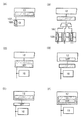
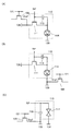
- FIGS. 3A to 3F are diagrams illustrating an adder circuit and a pixel.
- FIG. 4 is a diagram illustrating an addition circuit and a pixel.
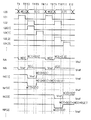
- FIG. 5 is a timing chart illustrating the operation of the addition circuit and the pixel.
- FIG. 6 is a timing chart illustrating the operation of the addition circuit and the pixel.
- FIGS. 7A to 7D are diagrams illustrating circuit blocks.
- FIGS. 8A to 8D are diagrams illustrating circuit blocks.
- FIGS. 9A to 9C are diagrams illustrating circuit blocks.
- FIG. 10 is a diagram illustrating an addition circuit and a pixel.
- FIG. 11 is a diagram illustrating a configuration of an adder circuit and a pixel used for a simulation.
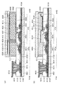
- FIG. 12 is a timing chart used for the simulation.
- FIG. 13 is a timing chart used for the simulation.
- FIG. 14 is a diagram illustrating the result of the simulation.
- FIG. 15 is a diagram illustrating the result of the simulation.
- FIGS. 16A to 16C are diagrams illustrating a display device.
- FIGS. 17A and 17B are diagrams illustrating a touch panel.
- FIGS. 18A and 18B are diagrams illustrating a display device.
- FIG. 19 is a diagram illustrating a display device.
- FIGS. 20A and 20B illustrate a display device.
- FIGS. 21A and 21B are diagrams illustrating a display device.
- FIGS. 22A to 22E are diagrams illustrating a display device.
- FIGS. 23A1 to 23C2 illustrate a transistor.
- FIGS. 24A1 to 24C2 illustrate a transistor.
- FIGS. 25A1 to 25C2 are diagrams illustrating a transistor.
- FIGS. 26A1 to 26C2 illustrate a transistor.
- FIGS. 27A to 27F are diagrams illustrating electronic devices.
- the element may be configured by a plurality of elements unless there is a functional inconvenience.
- a plurality of transistors operating as switches may be connected in series or in parallel.
- the capacitor may be divided and arranged at a plurality of positions.
- one conductor may have a plurality of functions such as a wiring, an electrode, and a terminal in some cases, and in this specification, a plurality of names may be used for the same element.
- a plurality of names may be used for the same element.
- the elements may actually be connected via a plurality of conductors in some cases. In this document, such a configuration is also included in the category of direct connection.
- One embodiment of the present invention is a display device including a circuit having a function of adding data (hereinafter, an addition circuit) and a pixel having a function of adding data.
- the addition circuit has a function of adding data supplied from the source driver.
- the pixel has a function of adding data supplied from the addition circuit. Therefore, the display device of one embodiment of the present invention can generate a voltage several times higher than the output voltage of the source driver and supply the generated voltage to the display device.
- the addition circuit is electrically connected to the pixels in the display area column direction, and some of the elements can be divided and arranged in the pixel area. Therefore, restrictions on the size of elements included in the addition circuit can be relaxed, and data can be added efficiently. In addition, by providing other elements included in the addition circuit outside the display region, the number of wirings in the display region can be reduced, and the aperture ratio can be increased in a pixel.
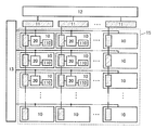
- FIG. 1 illustrates a display device of one embodiment of the present invention.
- the display device includes the pixels 10 arranged in the column direction and the row direction, a source driver 12, a gate driver 13, and a circuit 11.
- Source driver 12 is electrically connected to circuit 11.
- Gate driver 13 is electrically connected to pixel 10.
- the circuit 11 is electrically connected to the pixel 10.
- FIG. 1 shows an example in which one gate driver 13 is provided along one side of the display region 15, one more gate driver is provided along a side opposite to the one side, and a pixel driver is provided by two gate drivers. 10 may be driven.
- the circuit 11 can be provided for each column, and is electrically connected to all the pixels 10 arranged in the same column. Elements of the circuit 11 can be provided inside and outside the display area.
- the circuit 11 is an addition circuit, and has a function of adding first data and second data supplied from the source driver 12 by capacitive coupling to generate third data.
- the pixel 10 includes a circuit 20 and a circuit block 110.
- the circuit 20 has a function of adding the first data and the third data supplied from the adding circuit by capacitive coupling to generate fourth data. Alternatively, it has a function of adding the third data to the third data supplied from the adding circuit by capacitive coupling to generate fifth data.
- the circuit block 110 has a display device and has a function of performing display on the display device in accordance with the fourth data or the fifth data supplied from the circuit 20.
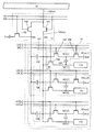
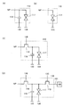
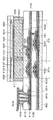
- FIG. 2 illustrates a circuit 11 and a pixel 10 (pixels 10 [m, 1] to 10 [m, n] (m and n are 1 or more) arranged in an arbitrary column (m-th column) of the display device illustrated in FIG. FIG.
- the circuit 11 can have a structure including the transistor 101, the transistor 102, the transistor 103, and the capacitor 107.
- One of a source and a drain of the transistor 101 is electrically connected to one electrode of the capacitor 107.
- the other electrode of the capacitor 107 is electrically connected to one of a source and a drain of the transistor 102.
- One of a source and a drain of the transistor 102 is electrically connected to one electrode of the transistor 103.
- the capacitor 107 can be configured by connecting a plurality of capacitors 108 in parallel. By distributing the capacitors 108 in the pixel region, the total area of the capacitors 107 can be easily increased. Further, the area occupied by the circuit 11 outside the display area can be reduced, and the frame can be narrow. Note that some capacitors 108 may be provided outside the display area. Further, the capacitor 108 may not be provided in all pixel regions. By adjusting the number of capacitors 108 connected in parallel, the capacitance value of the capacitor 107 can be set to a desired value.
- the capacitor 108 can have the wiring 125 as one electrode and another wiring overlapping with the wiring 125 as the other electrode. Therefore, even if the capacitor 108 is arranged in the pixel region as shown in FIG. 2, the aperture ratio does not significantly decrease.
- the pixel 10 can have a configuration including the circuit 20 and the circuit block 110. Further, as described above, the capacitor 108 can be arranged in the pixel region.
- the circuit 20 can have a structure including the transistor 104, the transistor 105, the transistor 106, and the capacitor 109.
- One of a source and a drain of the transistor 104 is electrically connected to one electrode of the capacitor 109.
- the other electrode of the capacitor 109 is electrically connected to one of a source and a drain of the transistor 105.
- One of a source and a drain of the transistor 105 is electrically connected to one of a source and a drain of the transistor 106.
- One of a source and a drain of the transistor 104 is electrically connected to the circuit block 110.
- the circuit block 110 can be configured to include a transistor, a capacitor, a display device, and the like, and details will be described later.
- the gate of the transistor 101 is electrically connected to the wiring 121.
- the gate of the transistor 102 is electrically connected to the wiring 122.
- the gate of the transistor 103 is electrically connected to the wiring 121.
- the gate of the transistor 104 is electrically connected to the wiring 123.
- the gate of the transistor 105 is electrically connected to the wiring 124.
- the gate of the transistor 106 is electrically connected to the wiring 123.
- One of a source and a drain of the transistor 101 is electrically connected to the wiring 125.
- the other of the source and the drain of the transistor 101 and the other of the source and the drain of the transistor 102 are electrically connected to the wiring 126.
- the other of the source and the drain of the transistor 103 and the other of the source and the drain of the transistor 106 are electrically connected to a wiring which can supply V ref (for example, a reference potential such as 0 V).
- the wirings 121, 122, and 123 (123 [1] to [n]) and the wiring 124 (124 [1] to [n]) have functions as gate lines.
- the wirings 121 and 122 can be electrically connected to a circuit that controls operation of the circuit 11.
- the wirings 123 and 124 can be electrically connected to the gate driver 13.
- the wiring 126 can be electrically connected to the source driver 12 (see FIG. 1).
- a wiring (wiring 125) connecting one of the source and the drain of the transistor 101, one electrode of the capacitor 107, and one of the source and the drain of the transistor 105 is referred to as a node NA.
- a wiring connecting one of the source or the drain of the transistor 102, one of the source or the drain of the transistor 103, and the other electrode of the capacitor 107 is referred to as a node NB.
- a wiring connecting one of the source and the drain of the transistor 105, one of the source and the drain of the transistor 106, and the other electrode of the capacitor 109 is referred to as a node NC.
- a wiring connecting one of the source and the drain of the transistor 104, one electrode of the capacitor 109, and the circuit block 110 is referred to as a node NP.
- the node NP can be floating, and the display device included in the circuit block 110 operates according to the potential of the node NP.
- first data (weight: W) is written to the node NA.
- “V ref ” is supplied to the other electrode of the capacitor 107, and “W ⁇ V ref ” is held in the capacitor 107.
- the node NA is floated, and the second data (data: D) is supplied to the node NB.
- the potential of the node NA is W + (C 107 / (C 107 + C NA )) ⁇ (D ⁇ V ref ).
- the potential of the node NA becomes "W + D-V ref" .
- the potential of the node NP is W + (C 109 / (C 109 + C NP )) ⁇ (2D ⁇ V ref ).
- the potential of the node NP becomes "W + 2D-V ref" .
- the pixel 10 can perform an operation different from that described above.
- “2D” is written to the node NA.
- “V ref ” is supplied to the other electrode of the capacitor 109, and “2D ⁇ V ref ” is held in the capacitor 109.
- the node NP is set to the floating state, and the third data (“2D”) is supplied to the node NC.
- the potential of the node NP is 2D + (C 109 / (C 109 + C NP )) ⁇ (2D ⁇ V ref ).
- the potential of the node NP becomes "2D + 2D-V ref" .
- a high voltage can be generated even when a general-purpose driver IC is used.
- a liquid crystal device that requires a high voltage for gradation control can be driven.
- the voltage supplied from the source driver 12 for driving a general liquid crystal device or a light emitting device can be reduced to about 1/3 to 1/4, so that the power consumption of the display device can be reduced. .
- correction data may be supplied as the first data (weight: W).
- W the first data
- the threshold voltage correction data of the transistor is supplied as the first data (weight: W). Then, the display quality may be improved.
- the first data (weight: W) and the second data (data: D) may be interchanged.
- the data potential generated by the circuit 11 is supplied to the specific pixel 10 as described above to determine the potential of the node NP.
- the potential of the node NP of each pixel 10 can be determined. That is, different image data can be supplied to each pixel 10.
- the nodes NA, NB, NC, and NP act as storage nodes. Data can be written to each node by turning on a transistor connected to each node. In addition, by turning off the transistor, the data can be held at each node.
- a transistor with extremely low off-state current is used as the transistor, leakage current can be suppressed and the potential of each node can be held for a long time.
- a transistor including a metal oxide for a channel formation region hereinafter, referred to as an OS transistor
- an OS transistor can be used as the transistor.
- an OS transistor it is preferable to apply an OS transistor to any or all of the transistors 101, 102, 103, 104, 105, and 106. Further, an OS transistor may be applied to an element included in the circuit block 110. In the case where operation is performed in a range where the amount of leakage current is allowable, a transistor including Si in a channel formation region (hereinafter, a Si transistor) may be used. Alternatively, an OS transistor and a Si transistor may be used in combination. Note that examples of the Si transistor include a transistor including amorphous silicon, a transistor including crystalline silicon (microcrystalline silicon, low-temperature polysilicon, and single-crystal silicon).
- a metal oxide having an energy gap of 2 eV or more, preferably 2.5 eV or more, more preferably 3 eV or more can be used.
- an oxide semiconductor containing indium or the like is used; for example, a CAAC-OS or a CAC-OS described later can be used.
- the CAAC-OS has stable atoms in its crystal and is suitable for a transistor or the like in which reliability is emphasized.
- the CAC-OS has high mobility characteristics, it is suitable for a transistor that drives at high speed or the like.
- the OS transistor has an extremely low off-current characteristic of several yA / ⁇ m (current value per 1 ⁇ m of channel width) because the energy gap of the semiconductor layer is large. Further, the OS transistor has characteristics different from those of the Si transistor, such as being free from impact ionization, avalanche breakdown, and a short-channel effect, and can form a highly reliable circuit. In addition, variation in electrical characteristics due to non-uniformity of crystallinity, which is a problem in the Si transistor, hardly occurs in the OS transistor.
- the semiconductor layer included in the OS transistor includes an In-M-Zn-based oxide including, for example, indium, zinc, and M (a metal such as aluminum, titanium, gallium, germanium, yttrium, zirconium, lanthanum, cerium, tin, neodymium, or hafnium). Can be obtained.
- M a metal such as aluminum, titanium, gallium, germanium, yttrium, zirconium, lanthanum, cerium, tin, neodymium, or hafnium.
- the oxide semiconductor included in the semiconductor layer is an In-M-Zn-based oxide
- the atomic ratio of metal elements in a sputtering target used for forming the In-M-Zn oxide is In ⁇ M
- Zn It is preferable to satisfy ⁇ M.
- each of the atomic ratios of the semiconductor layers to be formed includes a variation of ⁇ 40% of the atomic ratio of the metal element contained in the sputtering target.
- the semiconductor layer an oxide semiconductor with low carrier density is used.
- the semiconductor layer has a carrier density of 1 ⁇ 10 17 / cm 3 or less, preferably 1 ⁇ 10 15 / cm 3 or less, further preferably 1 ⁇ 10 13 / cm 3 or less, more preferably 1 ⁇ 10 11 / cm 3. 3 or less, more preferably less than 1 ⁇ 10 10 / cm 3 , and an oxide semiconductor with a carrier density of 1 ⁇ 10 ⁇ 9 / cm 3 or more can be used.
- Such an oxide semiconductor is referred to as a highly purified intrinsic or substantially highly purified intrinsic oxide semiconductor. It can be said that the oxide semiconductor has a low density of defect states and has stable characteristics.
- the composition is not limited thereto, and a transistor having an appropriate composition may be used depending on required semiconductor characteristics and electric characteristics (eg, field-effect mobility and threshold voltage) of the transistor.
- the carrier density, the impurity concentration, the defect density, the atomic ratio between a metal element and oxygen, the interatomic distance, the density, and the like be appropriate.
- the concentration of silicon or carbon (concentration obtained by secondary ion mass spectrometry) in the semiconductor layer is set to 2 ⁇ 10 18 atoms / cm 3 or less, preferably 2 ⁇ 10 17 atoms / cm 3 or less.
- an alkali metal and an alkaline earth metal may generate carriers when combined with an oxide semiconductor, which may increase off-state current of a transistor. Therefore, the concentration of alkali metal or alkaline earth metal in the semiconductor layer (concentration obtained by secondary ion mass spectrometry) is 1 ⁇ 10 18 atoms / cm 3 or less, preferably 2 ⁇ 10 16 atoms / cm 3 or less.
- the nitrogen concentration (concentration obtained by secondary ion mass spectrometry) in the semiconductor layer is preferably 5 ⁇ 10 18 atoms / cm 3 or less.
- oxygen when hydrogen is contained in the oxide semiconductor included in the semiconductor layer, oxygen reacts with oxygen bonded to a metal atom to become water, so that oxygen vacancies may be formed in the oxide semiconductor in some cases.
- oxygen vacancies are contained in a channel formation region in an oxide semiconductor, the transistor might have normally-on characteristics.
- a defect in which hydrogen is contained in an oxygen vacancy functions as a donor, and an electron serving as a carrier may be generated.
- part of hydrogen is bonded to oxygen which is bonded to a metal atom to generate an electron serving as a carrier. Therefore, a transistor including an oxide semiconductor containing a large amount of hydrogen is likely to have normally-on characteristics.
- a defect in which hydrogen is contained in an oxygen vacancy can function as a donor of an oxide semiconductor.
- an oxide semiconductor is evaluated not by a donor concentration but by a carrier concentration. Therefore, in this specification and the like, a carrier concentration which assumes a state where an electric field is not applied may be used instead of a donor concentration as a parameter of an oxide semiconductor in some cases. That is, the “carrier concentration” described in this specification and the like may be referred to as a “donor concentration” in some cases.
- the hydrogen concentration obtained by secondary ion mass spectrometry is lower than 1 ⁇ 10 20 atoms / cm 3 , preferably 1 ⁇ 10 19 atoms / cm 3. It is less than 3 , more preferably less than 5 ⁇ 10 18 atoms / cm 3 , further preferably less than 1 ⁇ 10 18 atoms / cm 3 .
- an oxide semiconductor in which impurities such as hydrogen are sufficiently reduced is used for a channel formation region of a transistor, stable electric characteristics can be provided.
- the semiconductor layer may have a non-single-crystal structure, for example.
- the non-single-crystal structure includes, for example, a CAAC-OS (C-Axis Aligned Crystalline Oxide Semiconductor) having a crystal oriented in the c-axis, a polycrystalline structure, a microcrystalline structure, or an amorphous structure.
- CAAC-OS C-Axis Aligned Crystalline Oxide Semiconductor
- the amorphous structure has the highest density of defect states
- the CAAC-OS has the lowest density of defect states.
- An oxide semiconductor film having an amorphous structure has, for example, disordered atomic arrangement and no crystalline component.
- an oxide film having an amorphous structure has, for example, a completely amorphous structure and no crystal part.
- the semiconductor layer is a mixed film including two or more of an amorphous structure region, a microcrystalline structure region, a polycrystalline structure region, a CAAC-OS region, and a single crystal structure region.
- the mixed film may have a single-layer structure or a stacked structure including any two or more of the above-described regions, for example.
- CAC cloud-aligned composite
- the CAC-OS is one structure of a material in which an element included in an oxide semiconductor is unevenly distributed in a size of, for example, 0.5 nm or more and 10 nm or less, preferably, 1 nm or more and 2 nm or less.
- one or more metal elements are unevenly distributed in an oxide semiconductor, and a region including the metal element has a size of 0.5 nm to 10 nm, preferably 1 nm to 2 nm, or a size in the vicinity thereof.
- the state mixed by is also referred to as a mosaic shape or a patch shape.
- the oxide semiconductor preferably contains at least indium. In particular, it preferably contains indium and zinc.
- a CAC-OS in an In-Ga-Zn oxide is an indium oxide (hereinafter referred to as InO).
- X1 (X1 is greater real than 0) and.), or indium zinc oxide (hereinafter, in X2 Zn Y2 O Z2 ( X2, Y2, and Z2 is larger real than 0) and a.), gallium Oxide (hereinafter, referred to as GaO X3 (X3 is a real number larger than 0)) or gallium zinc oxide (hereinafter, Ga X4 Zn Y4 O Z4 (X4, Y4, and Z4 are real numbers larger than 0)) and to.) and the like, the material becomes mosaic by separate into, mosaic InO X1 or in X2 Zn Y2 O Z2, is a configuration in which uniformly distributed in the film (hereinafter Also referred to as a cloud-like.) A.
- the CAC-OS is a composite oxide semiconductor having a structure in which a region containing GaO X3 as a main component and a region containing In X2 Zn Y2 O Z2 or InO X1 as a main component are mixed.
- the atomic ratio of In to the element M in the first region is larger than the atomic ratio of In to the element M in the second region.
- the concentration of In is higher than that of the region No. 2.
- IGZO is a common name and may refer to one compound of In, Ga, Zn, and O. Representative examples are represented by InGaO 3 (ZnO) m1 (m1 is a natural number), or In (1 + x0) Ga ( 1-x0) O 3 (ZnO) m0 (-1 ⁇ x0 ⁇ 1, m0 is an arbitrary number) Crystalline compounds are mentioned.
- the above crystalline compound has a single crystal structure, a polycrystal structure, or a CAAC structure.
- the CAAC structure is a crystal structure in which a plurality of IGZO nanocrystals have a c-axis orientation and are connected without being oriented in the ab plane.
- CAC-OS relates to a material structure of an oxide semiconductor.
- CAC-OS is a material composition containing In, Ga, Zn, and O, a region which is observed in the form of a nanoparticle mainly containing Ga as a part and a nanoparticle mainly containing In as a part.
- a region observed in a shape refers to a configuration in which each region is randomly dispersed in a mosaic shape. Therefore, in the CAC-OS, the crystal structure is a secondary element.
- the CAC-OS does not include a stacked structure of two or more kinds of films having different compositions.
- a structure including two layers of a film mainly containing In and a film mainly containing Ga is not included.
- the CAC-OS is divided into a region which is observed in the form of a nanoparticle mainly including the metal element and a nanoparticle mainly including In.
- the region observed in the form of particles refers to a configuration in which each of the regions is randomly dispersed in a mosaic shape.
- the CAC-OS can be formed by, for example, a sputtering method under conditions in which the substrate is not heated intentionally.
- a sputtering method any one or more selected from an inert gas (typically, argon), an oxygen gas, and a nitrogen gas is used as a deposition gas.
- an inert gas typically, argon
- oxygen gas typically, argon
- a nitrogen gas is used as a deposition gas.
- the flow rate ratio of the oxygen gas to the total flow rate of the film formation gas during the film formation is preferably as low as possible.
- the flow rate ratio of the oxygen gas is preferably from 0% to less than 30%, more preferably from 0% to 10%. .
- the CAC-OS is characterized in that a clear peak is not observed when measured using a ⁇ / 2 ⁇ scan by an Out-of-plane method, which is one of X-ray diffraction (X-ray diffraction) measurement methods. Have. That is, from the X-ray diffraction measurement, it is understood that the orientation in the a-b plane direction and the c-axis direction of the measurement region is not observed.
- the CAC-OS includes, in an electron beam diffraction pattern obtained by irradiating an electron beam (also referred to as a nanobeam electron beam) having a probe diameter of 1 nm, a region (ring region) having a high luminance in a ring shape and the ring region. Multiple bright spots are observed in the area. Accordingly, the electron diffraction pattern shows that the crystal structure of the CAC-OS has an nc (nano-crystal) structure having no orientation in a planar direction and a cross-sectional direction.
- an electron beam also referred to as a nanobeam electron beam
- GaO X3 is a main component in EDX mapping obtained using energy dispersive X-ray spectroscopy (EDX: Energy Dispersive X-ray spectrum). It can be confirmed that the region and the region containing In X2 Zn Y2 O Z2 or InO X1 as a main component are unevenly distributed and mixed.
- the CAC-OS has a different structure from an IGZO compound in which metal elements are uniformly distributed, and has different properties from the IGZO compound. That is, the CAC-OS is phase-separated into a region containing GaO X3 or the like as a main component and a region containing In X2 Zn Y2 O Z2 or InO X1 as a main component. Has a mosaic structure.
- a region in which In X2 Zn Y2 O Z2 or InO X1 is a main component is a region having higher conductivity than a region in which GaO X3 or the like is a main component. That is, when a carrier flows through a region containing In X2 Zn Y2 O Z2 or InO X1 as a main component, conductivity as an oxide semiconductor is exhibited. Therefore, high field-effect mobility ( ⁇ ) can be realized by distributing a region containing In X2 Zn Y2 O Z2 or InO X1 as a main component in a cloud shape in the oxide semiconductor.
- a region containing GaO X3 or the like as a main component is a region having higher insulating properties than a region containing In X2 Zn Y2 O Z2 or InO X1 as a main component. That is, a region in which GaO X3 or the like is a main component is distributed in the oxide semiconductor, so that a leak current can be suppressed and a favorable switching operation can be realized.
- the insulating property caused by GaO X3 and the like and the conductivity caused by In X2 Zn Y2 O Z2 or InO X1 act complementarily, so that high performance is obtained.
- On-state current (I on ) and high field-effect mobility ( ⁇ ) can be realized.
- CAC-OS is suitable as a constituent material of various semiconductor devices.
- elements other than the capacitor 107 of the circuit 11 may be incorporated in the source driver 12 as illustrated in FIG. With this configuration, the frame can be narrowed.
- a stack structure having a region where any of the elements of the source driver 12 and the circuit 11 overlap may be employed. With this configuration, the degree of freedom in designing the elements of the circuit 11 can be increased, and the electrical characteristics can be improved.
- FIG. 1 shows an example in which the circuit 11 is provided for each column.
- a selection circuit 16 is provided between the circuit 11 and the pixel 10 to provide data for pixels in a plurality of columns. May be performed by one circuit 11.
- FIG. 3B illustrates an example in which writing is performed on pixels in three columns using a combination of one circuit 11 and one selection circuit 16; Then, the number of columns may be determined.
- the capacitor 107 may be provided outside the display region together with the circuit 11 without being provided in the display region.
- a stack structure including a region where the circuit 11 and the capacitor 107 overlap may be employed. With such a structure, the aperture ratio of the pixel 10 can be increased.
- the capacitor 107 may be incorporated in the source driver 12.
- a stack structure having a region where the source driver 12 and the capacitor 107 overlap may be employed. With this configuration, the frame can be narrowed.
- a configuration in which the capacitor 107 is arranged outside the display region and the circuit 11 is incorporated in the source driver 12 may be employed.
- a stack structure having an area where the source driver 12 and the circuit 11 overlap may be employed. With such a structure, it is possible to narrow the frame and increase the aperture ratio of the pixel.
- the circuit 11 and the capacitor 107 may be incorporated in the source driver 12.
- a stack structure having a region where the source driver 12 overlaps with any of the circuit 11 and the capacitor 107 may be employed.
- a stack structure having a region where the source driver 12, the circuit 11, and the capacitor 107 overlap with each other may be employed. With this configuration, the frame can be narrowed.
- the transistors 101, 102, and 103 included in the circuit 11 are provided outside the display region; therefore, the size of the transistors 101, 102, and 103 is hardly limited, and the channel width can be larger than that of a transistor provided in a pixel. With the use of a transistor with a large channel width, the charge and discharge time for the wiring 125 and the like can be reduced, and the frame frequency can be easily increased. Further, the present invention can be easily applied to a high definition display having a large number of pixels and a short horizontal period.
- the circuit 11 can have a high withstand voltage, and stable operation can be performed even when a voltage generated in addition of data is several tens of volts.
- the transistors 101, 102, and 103 are Si transistors provided in an IC chip, higher-speed operation can be performed. Note that when the transistors 101, 102, and 103 are provided in an IC chip, the transistors may be OS transistors.
- the circuit 11 may be provided in both a region along one side of the display region 15 and a region along a side opposite to the one side, as shown in FIG.
- the circuit 11 provided on one side of the display area 15 is a circuit 11a.
- the operation of the circuit 11a is controlled by signals supplied from the wirings 121a and 122a.
- the circuit 11a is electrically connected to the source driver 12a.
- the circuit 11 provided on the side of the display area 15 opposite to the one side is a circuit 11b.
- the operation of the circuit 11b is controlled by signals supplied from the wirings 121b and 122b.
- the circuit 11b is electrically connected to the source driver 12b.
- the circuits 11a and 11b operate to output the same data at the same timing. That is, the same data is output from the source drivers 12a and 12b at the same timing, and the same operation signal is supplied to the wirings 121a and 121b or the wirings 122a and 122b at the same timing.
- the circuit 11a and the circuit 11b can be operated at the same time, and the same data can be output to the wiring 125. Therefore, the wiring 125 can be charged / discharged at high speed, and it is easy to correspond to a display device with a large number of pixels and a short horizontal period, a large display device with a large parasitic capacitance of the wiring 125, and the like.
- a high potential is represented by “H” and a low potential is represented by “L”.
- the weight supplied to the pixel 10 [1] is “W [1]”
- the image data is “D [1]”
- the weight supplied to the pixel 10 [2] is “W [2]”
- the image data is “W [2]”.
- D [2] ".
- V ref for example, 0 V, a GND potential, or a specific reference potential can be used.
- the transistors 101 and 104 are turned on, and the potential of the wiring 126 is written to the node NA. Further, the potential of the node NA is written to the node NP [1]. This operation is a weight writing operation in both the circuit 11 and the pixel 10, and the potentials of the node NA and the node NP [1] become “W [1]”.
- the transistor 105 is turned on.
- the potential of the node NC becomes “W [1] + D [1] ′” and “(W [1] + D [1] ′) according to the capacitance ratio between the node NC [1] and the node NP [1].
- “” Is added to the node NP [1].
- This operation is an addition operation in the pixel 10, and the potential of the node NP [1] is "W [1] + (W [1] + D [1] ' -Vref )'".
- the potential of the node NP [1] is supplied to a display device, and display is performed.
- W [1] D [1]
- the capacity of the node NA is sufficiently smaller than the capacity of the node NB
- the capacity of the node NP [1] is sufficiently smaller than the capacity of the node NC [1].
- “W [1] + (W [1] + D [1] ′) ′” is a value close to “3D [1]”. Therefore, a data potential that is about three times the data potential output by the source driver can be supplied to the display device.
- the pixel 10 [2] By applying the same operation to the pixel 10 [2] from time T5 to time T8, the pixel 10 [2] performs display according to “W [2] + (W [2] + D [2] ′) ′”. It can be performed.
- V ref is written to the node NC.
- This operation is a writing operation of a weight in the pixel 10 and a reset operation for capacitive coupling, and the potential of the node NP [1] becomes “W [1] + D [1] ′”.
- W [1] D [1]
- the capacity of the node NA is sufficiently smaller than the capacity of the node NB
- the capacity of the node NP [1] is sufficiently smaller than the capacity of the node NC [1].
- “W [1] + D [1] ′ + (W [1] + D [1] ′) ′” is a value close to “4D [1]”. Therefore, a data potential that is about four times the data potential output from the source driver can be supplied to the display device.
- FIGS. 7A to 7C illustrate an example of a structure which can be applied to the circuit block 110 and includes a light-emitting device as a display device.
- the structure illustrated in FIG. 7A includes a transistor 111, a capacitor 113, and a light-emitting device 114.
- One of a source and a drain of the transistor 111 is electrically connected to one electrode of the light-emitting device 114.
- One electrode of the light emitting device 114 is electrically connected to one electrode of the capacitor 113.
- the other electrode of capacitor 113 is electrically connected to the gate of transistor 111.
- the gate of the transistor 111 is electrically connected to the node NP.
- the other of the source and the drain of the transistor 111 is electrically connected to the wiring 128.
- the other electrode of the light-emitting device 114 is electrically connected to the wiring 129.
- the wirings 128 and 129 have a function of supplying power.
- the wiring 128 can supply high-potential power.
- the wiring 129 can supply a low-potential power supply.
- one electrode of the light-emitting device 114 is electrically connected to the wiring 128, and the other electrode of the light-emitting device 114 is electrically connected to the transistor 111 and the other of the source and the drain. May be.
- This configuration can be applied to another circuit block 110 including the light-emitting device 114.
- FIG. 7C illustrates a structure in which the transistor 112 is added to the structure of FIG.
- One of a source and a drain of the transistor 112 is electrically connected to one of a source and a drain of the transistor 111.
- the other of the source and the drain of the transistor 112 is electrically connected to one electrode of the light-emitting device 114.
- the gate of the transistor 112 is electrically connected to the wiring 127.
- the wiring 127 can function as a signal line for controlling conduction of the transistor 112.
- FIG. 7D illustrates a structure in which the transistor 115 is added to the structure of FIG.
- One of a source and a drain of the transistor 115 is electrically connected to one of a source and a drain of the transistor 111.
- the other of the source and the drain of the transistor 115 is electrically connected to the wiring 131.
- the gate of the transistor 115 is electrically connected to the wiring 132.
- the wiring 132 can function as a signal line for controlling conduction of the transistor 115.
- the wiring 131 can be electrically connected to a supply source of a specific potential such as a reference potential. By supplying a specific potential to one of the source and the drain of the transistor 111 from the wiring 131, writing of image data can be stabilized. Further, the light emission timing of the light emitting device 114 can be controlled.
- the wiring 131 can be connected to the circuit 120 and can have a function as a monitor line.
- the circuit 120 can have one or more of a supply source of the specific potential, a function of acquiring electric characteristics of the transistor 111, and a function of generating correction data.
- FIG. 8A to 8D illustrate an example of a structure which can be applied to the circuit block 110 and includes a liquid crystal device as a display device.
- FIG. 8A includes a capacitor 116 and a liquid crystal device 117.
- One electrode of the liquid crystal device 117 is electrically connected to one electrode of the capacitor 116.
- One electrode of capacitor 116 is electrically connected to node NP.
- the other electrode of the capacitor 116 is electrically connected to the wiring 133.
- the other electrode of the liquid crystal device 117 is electrically connected to the wiring 134.
- the wirings 133 and 134 have a function of supplying power.
- the wirings 133 and 134 can supply a reference potential such as GND or 0 V or an arbitrary potential.
- an OS transistor can be used as a transistor connected to the node NP. Since the OS transistor has extremely small leak current, display can be maintained for a relatively long time even if the capacitor 116 functioning as a storage capacitor is omitted. In addition to the structure of the transistor, it is effective to omit the capacitor 116 in a case where the display period can be shortened by high-speed operation, such as a field sequential drive. By eliminating the capacitor 116, the aperture ratio can be improved. Alternatively, the transmittance of the pixel can be improved.
- the operation of the liquid crystal device 117 starts when the potential of the node NP is determined to be equal to or higher than the operation threshold value of the liquid crystal device 117. Therefore, the display operation may start when the weight is written to the node NP, and the application may be limited. However, in the case of a transmissive liquid crystal display device, an unnecessary display operation is performed by using an operation such as turning off the backlight until the timing when the operation of adding the weight (W) and the data (D) is completed. However, the visual recognition can be suppressed.
- FIG. 8C illustrates a structure in which the transistor 118 is added to the structure of FIG.
- One of a source and a drain of the transistor 118 is electrically connected to one electrode of the capacitor 116.
- the other of the source and the drain of the transistor 118 is electrically connected to the node NP.
- the gate of the transistor 118 is electrically connected to the wiring 136.
- the wiring 136 can function as a signal line for controlling conduction of the transistor 118.
- the potential of the node NP is applied to the liquid crystal device 117 with the conduction of the transistor 118. Therefore, the operation of the liquid crystal device can be started at an arbitrary timing after the operation of adding the weight (W) and the data (D).
- the reset may be performed by, for example, supplying a reset potential to the wiring 125 and turning on the transistor 104 and the transistor 118 at the same time.
- FIG. 8D illustrates a structure in which a transistor 119 is added to the structure of FIG.
- One of a source and a drain of the transistor 119 is electrically connected to one electrode of the liquid crystal device 117.
- the other of the source and the drain of the transistor 119 is electrically connected to the wiring 131.
- the gate of the transistor 119 is electrically connected to the wiring 135.
- the wiring 135 can function as a signal line for controlling conduction of the transistor 119.
- the circuit 120 electrically connected to the wiring 131 is similar to that described with reference to FIG. 7D and may have a function of resetting the potential supplied to the capacitor 116 and the liquid crystal device 117. .
- FIGS. 9A to 9C are diagrams illustrating specific examples of wiring for supplying “V ref ” in the pixel 10 illustrated in FIG. 2 and the like.
- the wiring 128 can be used as a wiring for supplying “V ref ”. Since “V ref ” is preferably 0 V, GND, or a low potential, the wiring 128 also has a function of supplying at least one of those potentials. “V ref ” may be supplied to the wiring 128 at the timing of writing data to the node NP, and a high-potential power supply may be supplied at the timing of causing the light-emitting device 114 to emit light.
- a wiring 129 for supplying a low potential may be used as a wiring for supplying “V ref ”.
- a wiring 133 can be used as a wiring for supplying “V ref ”.
- the wiring 134 may be applied. Note that a dedicated common line for supplying “V ref ” may be provided regardless of the type of the display device.
- a transistor may be provided with a back gate.
- FIG. 10 illustrates a configuration in which the back gate is electrically connected to the front gate, which has an effect of increasing the on-state current.
- a structure in which the back gate is electrically connected to a wiring which can supply a constant potential may be employed. With such a structure, the threshold voltage of the transistor can be controlled.
- a back gate may be provided for a transistor included in the circuit block 110.
- FIG. 11 shows the configuration of the pixel (PIX) and the circuit 11 used in the simulation. Assuming that the number of pixels is four, the configuration (liquid crystal device and capacitor) shown in FIG. The simulation was performed on the voltage change of the node NP of each pixel in the operation of increasing the input voltage by about three times (hereinafter, operation 1) and the operation of boosting the input voltage by about four times (hereinafter, operation 2).
- the capacitance value of the capacitor C1 was 500 pF
- the capacitance value of the capacitor C2 was 5 pF
- the capacitance value of the capacitor Cs was 500 fF
- the capacitance value of the liquid crystal device Clc was 500 fF.
- the voltage applied to the gate of the transistor was +15 V for "H” and -15 V for "L”.
- the capacitance value of the capacitor C1 was 100 pF
- the capacitance value of the capacitor C2 was 10 pF
- the capacitance value of the capacitor Cs was 50 fF
- the capacitance value of the liquid crystal device Clc was 50 fF.
- the voltage applied to the gate of the transistor was +15 V for "H” and -20 V for "L".
- the wiring PL connecting the circuit 11 and the pixel PIX include the same number of resistors R1 corresponding to parasitic resistance and the same number of capacitors C3 corresponding to parasitic capacitance as the number of pixels.
- the parasitic capacitance (sum of C3) of the wiring PL was 0F and the resistance (sum of R1) of the wiring PL was 0 ⁇ .
- SPICE was used as the circuit simulation software.
- FIG. 12 is a timing chart used for the simulation of the operation 1.
- FIG. 13 is a timing chart used for the simulation of the operation 2.
- Weight (+ W), data (+ D) were +5 V
- weight (-W) were +5 V as parameters common to the operations 1 and 2.
- the potentials of V ref , VCOM, and TCOM were all set to 0V.
- the horizontal axis represents time (second), and the vertical axis represents the voltage (V) of the node NP.
- Each figure shows, on a time axis, a change in voltage at the node NP when a writing operation is performed on the pixels PIX [1] to PIX [4].
- This embodiment can be implemented in appropriate combination with the structures described in the other embodiments and the like.
- Embodiment 2 In this embodiment, a configuration example of a display device using a liquid crystal device and a configuration example of a display device using a light-emitting device will be described. Note that, in this embodiment, descriptions of the elements, operations, and functions of the display device described in Embodiment 1 are omitted.
- the display device described in this embodiment can use the addition circuit and the pixel described in Embodiment 1.
- a scanning line driver circuit described below corresponds to a gate driver
- a signal line driver circuit corresponds to a source driver.
- FIGS. 16A to 16C illustrate a structure of a display device to which one embodiment of the present invention can be applied.
- a sealant 4005 is provided so as to surround a display portion 215 provided over a first substrate 4001, and the display portion 215 is sealed with the sealant 4005 and the second substrate 4006. .
- the scan line driver circuit 221a, the signal line driver circuit 231a, the signal line driver circuit 232a, and the common line driver circuit 241a each include a plurality of integrated circuits 4042 provided over a printed board 4041.
- the integrated circuit 4042 is formed using a single crystal semiconductor or a polycrystalline semiconductor.
- the common line driver circuit 241a has a function of supplying a prescribed potential to the wirings 128, 129, 133, and 134 described in Embodiment 1.
- the integrated circuit 4042 included in the scan line driver circuit 221a and the common line driver circuit 241a has a function of supplying a selection signal to the display portion 215.
- the integrated circuit 4042 included in the signal line driver circuits 231a and 232a has a function of supplying image data to the display portion 215.
- the integrated circuit 4042 is mounted in a region on the first substrate 4001 which is different from a region surrounded by the sealant 4005.
- a method for connecting the integrated circuit 4042 and a wire bonding method, a COG (Chip On Glass) method, a TCP (Tape Carrier Package) method, a COF (Chip On Film) method, or the like can be used. it can.
- a COG Chip On Glass
- TCP Transmission Carrier Package
- COF Chip On Film
- FIG. 16B illustrates an example in which the integrated circuit 4042 included in the signal line driver circuit 231a and the signal line driver circuit 232a is mounted by a COG method. Further, part or the whole of the driver circuit can be formed over the same substrate as the display portion 215, whereby a system-on-panel can be formed.
- FIG. 16B illustrates an example in which the scan line driver circuit 221a and the common line driver circuit 241a are formed over the same substrate as the display portion 215.
- a sealant 4005 is provided so as to surround the display portion 215 provided over the first substrate 4001, the scan line driver circuit 221a, and the common line driver circuit 241a.
- a second substrate 4006 is provided over the display portion 215, the scan line driver circuit 221a, and the common line driver circuit 241a. Therefore, the display portion 215, the scan line driver circuit 221a, and the common line driver circuit 241a are sealed with the first substrate 4001, the sealant 4005, and the second substrate 4006.
- FIG. 16B illustrates an example in which the signal line driver circuit 231a and the signal line driver circuit 232a are separately formed and mounted on the first substrate 4001; however, this embodiment is not limited to this structure.
- the scan line driver circuit may be formed separately and mounted, or a part of the signal line driver circuit or a part of the scan line driver circuit may be formed separately and mounted.
- the signal line driver circuit 231a and the signal line driver circuit 232a may be formed over the same substrate as the display portion 215.
- the display device may include a panel in which the display device is sealed and a module in which an IC or the like including a controller is mounted on the panel.
- the display portion and the scan line driver circuit provided over the first substrate have a plurality of transistors.
- the transistor the transistor described in the above embodiment can be used.
- the structure of the transistor included in the peripheral driver circuit and the structure of the transistor included in the pixel circuit in the display portion may be the same or different.
- the transistors included in the peripheral driver circuit may all have the same structure, or may be a combination of two or more types of structures.
- all the transistors included in the pixel circuit may have the same structure or a combination of two or more types of structures.
- the input device 4200 can be provided over the second substrate 4006.
- the structure in which the input device 4200 is provided in the display device illustrated in FIGS. 16A to 16C can function as a touch panel.
- sensing element also referred to as a sensor element
- Various sensors that can detect the proximity or contact of a detection target such as a finger or a stylus can be applied as the detection element.
- a sensor system for example, various systems such as a capacitance system, a resistance film system, a surface acoustic wave system, an infrared system, an optical system, and a pressure-sensitive system can be used.
- a touch panel having a capacitance type sensing element will be described as an example.
- Examples of the capacitance type include a surface type capacitance type and a projection type capacitance type.
- the projection-type capacitance method includes a self-capacitance method, a mutual capacitance method, and the like. It is preferable to use the mutual capacitance method because simultaneous multipoint detection becomes possible.
- the touch panel of one embodiment of the present invention has a structure in which a separately manufactured display device and a sensing element are attached to each other, a structure in which an electrode or the like constituting a sensing element is provided on one or both of a substrate supporting a display device and a counter substrate, or the like.
- Various configurations can be applied.
- FIGS. 17A and 17B illustrate an example of a touch panel.
- FIG. 17A is a perspective view of the touch panel 4210.
- FIG. 17B is a schematic perspective view of the input device 4200. Note that only representative components are shown for clarity.
- the touch panel 4210 has a configuration in which a display device and a sensing element which are separately manufactured are attached to each other.
- the touch panel 4210 includes an input device 4200 and a display device, which are provided in an overlapping manner.
- the input device 4200 includes a substrate 4263, an electrode 4227, an electrode 4228, a plurality of wirings 4237, a plurality of wirings 4238, and a plurality of wirings 4239.
- the electrode 4227 can be electrically connected to the wiring 4237 or the wiring 4239.
- the electrode 4228 can be electrically connected to the wiring 4238.
- the FPC 4272b is electrically connected to each of the plurality of wirings 4237, 4238, and 4239.
- the FPC 4272b can be provided with an IC 4273b.
- a touch sensor may be provided between the first substrate 4001 and the second substrate 4006 of the display device.
- a touch sensor is provided between the first substrate 4001 and the second substrate 4006, an optical touch sensor using a photoelectric conversion element may be used in addition to a capacitive touch sensor.
- FIGS. 18A and 18B are cross-sectional views of a portion indicated by a chain line of N1-N2 in FIG. 16B.
- the display device illustrated in FIGS. 18A and 18B includes an electrode 4015, and the electrode 4015 is electrically connected to a terminal included in the FPC 4018 through an anisotropic conductive layer 4019.
- the electrode 4015 is electrically connected to the wiring 4014 in openings formed in the insulating layers 4112, 4111, and 4110.
- the electrode 4015 is formed using the same conductive layer as the first electrode layer 4030, and the wiring 4014 is formed using the same conductive layer as the source and drain electrodes of the transistor 4010 and the transistor 4011.
- the display portion 215 and the scan line driver circuit 221a provided over the first substrate 4001 have a plurality of transistors.
- a transistor 4010 included in the display portion 215 is included.
- a transistor 4011 included in the scanning line driver circuit 221a is included. Note that although a bottom-gate transistor is illustrated as the transistor 4010 and the transistor 4011 in FIGS. 18A and 18B, a top-gate transistor may be used.
- an insulating layer 4112 is provided over the transistor 4010 and the transistor 4011.
- a partition 4510 is formed over the insulating layer 4112.
- the transistor 4010 and the transistor 4011 are provided over the insulating layer 4102.
- the transistor 4010 and the transistor 4011 each include an electrode 4017 formed over the insulating layer 4111.
- the electrode 4017 can function as a back gate electrode.
- the display device illustrated in FIGS. 18A and 18B includes a capacitor 4020.
- the capacitor 4020 includes an electrode 4021 formed in the same step as the gate electrode of the transistor 4010, and an electrode formed in the same step as the source and drain electrodes. These electrodes overlap with an insulating layer 4103 interposed therebetween.
- the capacitance of a capacitor provided in a pixel portion of a display device is set so as to hold electric charge for a predetermined period in consideration of a leak current or the like of a transistor provided in the pixel portion.
- the capacity of the capacitor may be set in consideration of the off-state current or the like of a transistor electrically connected to the capacitor.
- FIG. 18A illustrates an example of a liquid crystal display device using a liquid crystal device as a display device.
- a liquid crystal device 4013 which is a display device includes a first electrode layer 4030, a second electrode layer 4031, and a liquid crystal layer 4008.
- an insulating layer 4032 and an insulating layer 4033 functioning as alignment films are provided so as to sandwich the liquid crystal layer 4008.
- the second electrode layer 4031 is provided on the second substrate 4006 side, and the first electrode layer 4030 and the second electrode layer 4031 overlap with each other with the liquid crystal layer 4008 interposed therebetween.
- liquid crystal devices to which various modes are applied can be used.
- a VA (Vertical Alignment) mode a TN (Twisted Nematic) mode, an IPS (In-Plane-Switching) mode, an ASM (Axially Symmetrical Aligned Microelectronic Cellular Cruiser Electronics Co., Ltd. ) Mode, AFLC (Anti Ferro Electric Liquid Crystal) mode, ECB (Electrically Controlled Birefringence) mode, VA-IPS mode, guest host mode, or the like can be used.
- a normally black liquid crystal display device such as a transmissive liquid crystal display device employing a vertical alignment (VA) mode may be applied to the liquid crystal display device described in this embodiment.
- VA vertical alignment
- an MVA (Multi-Domain Vertical Alignment) mode a PVA (Patterned Vertical Alignment) mode, an ASV (Advanced Super View) mode, or the like can be used.
- a liquid crystal device is an element that controls transmission or non-transmission of light by an optical modulation action of liquid crystal.
- the optical modulation action of the liquid crystal is controlled by an electric field (including a horizontal electric field, a vertical electric field, or an oblique electric field) applied to the liquid crystal.
- an electric field including a horizontal electric field, a vertical electric field, or an oblique electric field
- a thermotropic liquid crystal a low molecular liquid crystal
- a polymer liquid crystal a polymer dispersed liquid crystal (PDLC: Polymer Dispersed Liquid Crystal)
- ferroelectric liquid crystal an antiferroelectric liquid crystal, or the like
- These liquid crystal materials show a cholesteric phase, a smectic phase, a cubic phase, a chiral nematic phase, an isotropic phase, or the like depending on conditions.
- FIG. 18A illustrates an example of a liquid crystal display device including a vertical electric field liquid crystal device; however, a liquid crystal display device including a horizontal electric field liquid crystal device can be applied to one embodiment of the present invention.
- a liquid crystal exhibiting a blue phase without using an alignment film may be used.
- the blue phase is one of the liquid crystal phases, and is a phase that appears when the temperature of the cholesteric liquid crystal is raised immediately before the transition from the cholesteric phase to the isotropic phase. Since the blue phase appears only in a narrow temperature range, a liquid crystal composition in which a chiral agent of 5% by weight or more is mixed is used for the liquid crystal layer 4008 in order to improve the temperature range.
- a liquid crystal composition containing a liquid crystal exhibiting a blue phase and a chiral agent has a short response speed and exhibits optical isotropy. Further, a liquid crystal composition containing a liquid crystal exhibiting a blue phase and a chiral agent does not require an alignment treatment and has a small viewing angle dependence. Further, since it is not necessary to provide an alignment film, rubbing treatment is not required, so that electrostatic breakdown caused by the rubbing treatment can be prevented, and defects or breakage of a liquid crystal display device during a manufacturing process can be reduced. .
- the spacer 4035 is a columnar spacer obtained by selectively etching an insulating layer, and is provided for controlling a distance (cell gap) between the first electrode layer 4030 and the second electrode layer 4031. ing. Note that a spherical spacer may be used.
- a black matrix light-shielding layer
- a coloring layer color filter
- an optical member optical substrate
- circularly polarized light from a polarizing substrate and a retardation substrate may be used.
- a backlight, a sidelight, or the like may be used as a light source.
- a micro LED or the like may be used as the backlight and the sidelight.
- a light-blocking layer 4132, a coloring layer 4131, and an insulating layer 4133 are provided between the substrate 4006 and the second electrode layer 4031.
- Examples of a material that can be used as the light-shielding layer include carbon black, titanium black, a metal, a metal oxide, and a composite oxide containing a solid solution of a plurality of metal oxides.
- the light shielding layer may be a film containing a resin material or a thin film of an inorganic material such as a metal.
- a stacked film of a film containing a material used for the coloring layer can be used for the light-blocking layer.
- a stacked structure of a film containing a material used for a colored layer transmitting light of a certain color and a film containing a material used for a colored layer transmitting light of another color can be employed. It is preferable to use a common material for the coloring layer and the light-shielding layer, because the device can be shared and the process can be simplified.
- Examples of a material that can be used for the coloring layer include a metal material, a resin material, and a resin material containing a pigment or a dye.
- the formation of the light-shielding layer and the colored layer may be performed in the same manner as the formation of each layer described above. For example, it may be performed by an inkjet method or the like.
- the display device illustrated in FIGS. 18A and 18B includes an insulating layer 4111 and an insulating layer 4104.
- an insulating layer 4111 and the insulating layer 4104 an insulating layer which does not easily transmit an impurity element is used. By sandwiching the semiconductor layer of the transistor between the insulating layer 4111 and the insulating layer 4104, entry of impurities from the outside can be prevented.
- a light-emitting device can be used as a display device included in the display device.
- an EL element utilizing electroluminescence can be used.
- An EL element includes a layer containing a light-emitting compound (also referred to as an “EL layer”) between a pair of electrodes. When a potential difference larger than the threshold voltage of the EL element is generated between the pair of electrodes, holes are injected into the EL layer from the anode side and electrons are injected from the cathode side. The injected electrons and holes are recombined in the EL layer, and the light-emitting substance contained in the EL layer emits light.
- EL elements are distinguished depending on whether the light-emitting material is an organic compound or an inorganic compound. Generally, the former is called an organic EL element and the latter is called an inorganic EL element.
- an organic EL element In an organic EL element, electrons are injected from one electrode and holes are injected from the other electrode into the EL layer by applying a voltage. Then, by recombination of the carriers (electrons and holes), the light-emitting organic compound forms an excited state, and the organic compound emits light when the excited state returns to the ground state. Due to such a mechanism, such a light emitting device is called a current excitation type light emitting device.
- the EL layer is formed using a substance having a high hole-injection property, a substance having a high hole-transport property, a hole-blocking material, a substance having a high electron-transport property, a substance having a high electron-injection property, or a bipolar substance. (A substance having a high electron-transport property and a high hole-transport property) or the like.
- the EL layer can be formed by a method such as an evaporation method (including a vacuum evaporation method), a transfer method, a printing method, an inkjet method, and a coating method.
- a method such as an evaporation method (including a vacuum evaporation method), a transfer method, a printing method, an inkjet method, and a coating method.
- Inorganic EL elements are classified according to their element structures into a dispersion-type inorganic EL element and a thin-film inorganic EL element.
- the dispersion-type inorganic EL element has a light-emitting layer in which particles of a light-emitting material are dispersed in a binder.
- the light-emission mechanism is donor-acceptor recombination light emission using a donor level and an acceptor level.
- the thin-film inorganic EL device has a structure in which a light emitting layer is sandwiched between dielectric layers and further sandwiched between electrodes, and the light emission mechanism is localized light emission using inner-shell electron transition of metal ions. Note that here, an organic EL element will be described as a light emitting device.
- the light emitting device only needs to be transparent at least one of the pair of electrodes in order to extract light emission. Then, a transistor and a light emitting device are formed over the substrate, and a top emission (top emission) structure for extracting light emission from a surface opposite to the substrate, a bottom emission (bottom emission) structure for extracting light emission from a surface on the substrate side, and the like. There is a light emitting device having a dual emission (dual emission) structure in which light is emitted from both surfaces, and any light emitting device having an emission structure can be applied.
- FIG. 18B illustrates an example of a light-emitting display device using a light-emitting device as a display device (also referred to as an “EL display device”).
- a light-emitting device 4513 which is a display device is electrically connected to the transistor 4010 provided in the display portion 215.
- the structure of the light-emitting device 4513 is a stacked structure of the first electrode layer 4030, the light-emitting layer 4511, and the second electrode layer 4031; however, the structure is not limited to this.
- the structure of the light-emitting device 4513 can be changed as appropriate depending on the direction of light extracted from the light-emitting device 4513 and the like.
- the partition 4510 is formed using an organic insulating material or an inorganic insulating material.
- an opening be formed on the first electrode layer 4030 using a photosensitive resin material, and that the side surface of the opening be formed as an inclined surface having a continuous curvature.
- the light-emitting layer 4511 may be formed of a single layer or a structure in which a plurality of layers are stacked.
- the light-emitting color of the light-emitting device 4513 can be white, red, green, blue, cyan, magenta, yellow, or the like depending on the material of the light-emitting layer 4511.
- a method for achieving color display there are a method in which a light-emitting device 4513 emitting white light is combined with a coloring layer, and a method in which a light-emitting device 4513 having a different emission color is provided for each pixel.
- the former method is more productive than the latter method.
- the latter method since the light emitting layer 4511 needs to be separately formed for each pixel, the productivity is lower than the former method.
- the latter method can provide a luminescent color with higher color purity than the former method.
- the color purity can be further increased.
- the light-emitting layer 4511 may include an inorganic compound such as a quantum dot.
- an inorganic compound such as a quantum dot.
- a quantum dot for a light emitting layer, it can be made to function as a light emitting material.
- a protective layer may be formed over the second electrode layer 4031 and the partition 4510 so that oxygen, hydrogen, moisture, carbon dioxide, and the like do not enter the light-emitting device 4513.
- the protective layer silicon nitride, silicon nitride oxide, aluminum oxide, aluminum nitride, aluminum oxynitride, aluminum nitride oxide, DLC (Diamond Like Carbon), or the like can be formed.
- a filler 4514 is provided and sealed.
- a protective film a laminated film, an ultraviolet curable resin film, or the like
- a cover material that has high airtightness and low degassing so as not to be exposed to the outside air.
- an ultraviolet curable resin or a thermosetting resin in addition to an inert gas such as nitrogen or argon, an ultraviolet curable resin or a thermosetting resin can be used.
- PVC polyvinyl chloride
- acrylic resin acrylic resin
- polyimide polyimide
- epoxy resin epoxy resin
- silicone resin polyimide
- EVA ethylene vinyl acetate
- a desiccant may be included in the filler 4514.
- a glass material such as a glass frit, or a resin material such as a two-component resin that cures at room temperature, a photocurable resin, or a thermosetting resin can be used. Further, a desiccant may be included in the sealant 4005.
- an optical film such as a polarizing plate, a circularly polarizing plate (including an elliptically polarizing plate), a retardation plate ( ⁇ / 4 plate, ⁇ / 2 plate), and a color filter may be provided on the emission surface of the light emitting device. It may be provided as appropriate. Further, an antireflection film may be provided on a polarizing plate or a circularly polarizing plate. For example, anti-glare treatment can be performed in which reflected light is diffused by unevenness on the surface to reduce glare.
- the light-emitting device has a microcavity structure
- light with high color purity can be extracted.
- reflection can be reduced and visibility of a displayed image can be improved.
- a first electrode layer and a second electrode layer (also referred to as a pixel electrode layer, a common electrode layer, a counter electrode layer, and the like) for applying a voltage to a display device, a direction of light to be extracted, a place where the electrode layer is provided, and Light transmission or reflection may be selected depending on the pattern structure of the electrode layer.
- the first electrode layer 4030 and the second electrode layer 4031 are formed using indium oxide containing tungsten oxide, indium zinc oxide containing tungsten oxide, indium oxide containing titanium oxide, indium tin oxide, and indium containing titanium oxide.
- a light-transmitting conductive material such as tin oxide, indium zinc oxide, or indium tin oxide to which silicon oxide is added can be used.
- the first electrode layer 4030 and the second electrode layer 4031 are made of tungsten (W), molybdenum (Mo), zirconium (Zr), hafnium (Hf), vanadium (V), niobium (Nb), and tantalum (Ta).
- Metal such as chromium (Cr), cobalt (Co), nickel (Ni), titanium (Ti), platinum (Pt), aluminum (Al), copper (Cu), silver (Ag), or an alloy thereof It can be formed using one or more kinds of metal nitride.
- the first electrode layer 4030 and the second electrode layer 4031 can be formed using a conductive composition including a conductive high molecule (also referred to as a conductive polymer).
- a conductive high molecule also referred to as a conductive polymer.
- a so-called ⁇ -electron conjugated conductive high molecule can be used.
- polyaniline or a derivative thereof, polypyrrole or a derivative thereof, polythiophene or a derivative thereof, and a copolymer of two or more of aniline, pyrrole, and thiophene or a derivative thereof, and the like can be given.
- a protection circuit for protecting a driver circuit is preferably provided.
- the protection circuit is preferably formed using a non-linear element.
- FIG. 19 illustrates an example in which the stack structure is applied to the liquid crystal display device illustrated in FIG. 18A; however, the liquid crystal display device illustrated in FIG. 18B may be applied to an EL display device.
- a conductive film having a high light-transmitting property with respect to visible light for an electrode or a wiring by using a conductive film having a high light-transmitting property with respect to visible light for an electrode or a wiring, light transmittance in a pixel can be increased, and an aperture ratio can be substantially improved. it can.
- the semiconductor layer when an OS transistor is used, the semiconductor layer also has a light-transmitting property; thus, the aperture ratio can be further increased.
- a display device may be configured by combining a liquid crystal display device and a light emitting device.
- the light emitting device is arranged on the opposite side of the display surface or at the end of the display surface.
- the light-emitting device has a function of supplying light to a display device.
- the light-emitting device can also be called a backlight.
- the light-emitting device can include a plate-shaped or sheet-shaped light guide portion (also referred to as a light guide plate) and a plurality of light-emitting devices that emit light of different colors.
- a plate-shaped or sheet-shaped light guide portion also referred to as a light guide plate
- a plurality of light-emitting devices that emit light of different colors.
- the light guide has a mechanism for changing the optical path (also referred to as a light extraction mechanism), whereby the light emitting device can uniformly irradiate the pixel portion of the display panel with light.
- a structure in which a light emitting device is arranged immediately below a pixel without providing a light guide portion may be employed.
- the light emitting device has light emitting devices of three colors of red (R), green (G), and blue (B). Further, a white (W) light emitting device may be provided. It is preferable to use a light emitting diode (LED: Light Emitting Diode) as these light emitting devices.
- LED Light Emitting Diode
- the light emitting device has a full width at half maximum (FWHM: Full Width at at Half Maximum) of 50 nm or less, preferably 40 nm or less, more preferably 30 nm or less, and still more preferably 20 nm or less. It is preferably a light emitting device.
- FWHM Full Width at at Half Maximum
- the full width at half maximum of the emission spectrum is preferably as small as possible, but may be, for example, 1 nm or more. Thereby, when performing color display, a vivid display with high color reproducibility can be performed.
- the red light-emitting device it is preferable to use an element whose emission spectrum has a peak wavelength in a range from 625 nm to 650 nm.
- the green light-emitting device it is preferable to use an element having a peak wavelength of an emission spectrum in a range of 515 nm to 540 nm.
- the blue light-emitting device it is preferable to use an element whose peak wavelength of the emission spectrum is in the range of 445 nm to 470 nm.
- the display device blinks the light emitting devices of three colors sequentially, drives the pixels in synchronization with the light emitting devices, and performs color display based on the successive additive color mixing method.
- the driving method can also be referred to as field sequential driving.
- a vivid color image can be displayed.
- a smooth moving image can be displayed.
- one pixel does not need to be formed of a plurality of sub-pixels of different colors, and the effective reflection area (also referred to as an effective display area or an aperture ratio) of one pixel can be increased. Display can be performed. Further, since it is not necessary to provide a color filter for the pixel, the transmittance of the pixel can be improved, and a brighter display can be performed. Further, the manufacturing process can be simplified, and manufacturing cost can be reduced.
- 20A and 20B are examples of schematic cross-sectional views of a display device capable of performing field sequential driving.
- a backlight unit capable of emitting light of each color of RGB is provided on the substrate 4001 side of the display device.
- a color filter is unnecessary.
- a backlight unit 4340a illustrated in FIG. 20A has a structure in which a plurality of light-emitting devices 4342 are provided directly below a pixel with a diffusion plate 4352 interposed therebetween.
- the diffusion plate 4352 has a function of diffusing light emitted from the light-emitting device 4342 to the substrate 4001 side and uniforming luminance in a display portion surface.
- a polarizing plate may be provided between the light emitting device 4342 and the diffusion plate 4352 as needed.
- the diffusion plate 4352 may not be provided if unnecessary. Further, the light-blocking layer 4132 may be omitted.
- the backlight unit 4340a can include a large number of light-emitting devices 4342, bright display can be performed. Further, a light guide plate is unnecessary, and there is an advantage that the light efficiency of the light emitting device 4342 is hardly impaired. Note that the light emitting device 4342 may be provided with a light diffusion lens 4344 as needed.
- a backlight unit 4340b illustrated in FIG. 20B has a structure in which a light guide plate 4341 is provided directly below a pixel with a diffusion plate 4352 therebetween. At an end of the light guide plate 4341, a plurality of light emitting devices 4342 are provided.
- the light guide plate 4341 has a concavo-convex shape on the side opposite to the diffusion plate 4352, and can scatter the guided light in the concavo-convex shape and emit the light toward the diffusion plate 4352.
- the light emitting device 4342 can be fixed to the printed board 4347. Note that in FIG. 20B, the light emitting devices 4342 of each color of RGB are illustrated so as to overlap with each other, but the light emitting devices 4342 of each color of RGB can be arranged in the depth direction.
- a reflective layer 4348 that reflects visible light may be provided on a side surface opposite to the light emitting device 4342.
- the backlight unit 4340b can be reduced in cost and thickness.
- a light scattering type liquid crystal device may be used as the liquid crystal device.
- the light-scattering liquid crystal device an element having a composite material of liquid crystal and a polymer is preferably used.
- a polymer dispersed liquid crystal device can be used.
- a polymer network type liquid crystal (PNLC (Polymer Network Liquid Crystal)) element may be used.
- the light scattering type liquid crystal device has a structure in which a liquid crystal portion is provided in a three-dimensional network structure of a resin portion sandwiched between a pair of electrodes.
- a material used for the liquid crystal portion for example, a nematic liquid crystal can be used.
- a photocurable resin can be used as the resin portion.
- a monofunctional monomer such as acrylate and methacrylate
- a polyfunctional monomer such as diacrylate, triacrylate, dimethacrylate, and trimethacrylate, or a polymerizable compound obtained by mixing these can be used.
- the light scattering type liquid crystal device performs display by transmitting or scattering light by utilizing anisotropy of a refractive index of a liquid crystal material. Further, the resin portion may also have anisotropy of the refractive index.
- the liquid crystal molecules are arranged in a certain direction according to the voltage applied to the light scattering type liquid crystal device, a direction in which the difference in the refractive index between the liquid crystal part and the resin part becomes small occurs, and light incident along the direction is generated in the liquid crystal part. Transmit without scattering. Therefore, the light scattering type liquid crystal device is visually recognized in a transparent state from the direction.
- the light scattering type liquid crystal device is in an opaque state regardless of the viewing direction.
- FIG. 21A illustrates a structure in which the liquid crystal device 4013 of the display device in FIG. 20A is replaced with a light-scattering liquid crystal device 4016.
- the light-scattering liquid crystal device 4016 includes a composite layer 4009 having a liquid crystal portion and a resin portion, and electrode layers 4030 and 4031. Elements related to field sequential driving are the same as those in FIG. 20A. However, when the light scattering type liquid crystal device 4016 is used, an alignment film and a polarizing plate are not required.
- the spacer 4035 is illustrated in a spherical shape, it may be in a column shape.
- FIG. 21B illustrates a structure in which the liquid crystal device 4013 of the display device in FIG. 20B is replaced with a light-scattering liquid crystal device 4016.
- the light-scattering liquid crystal device 4016 operate in a mode in which light is transmitted when no voltage is applied and light is scattered when a voltage is applied.
- a transparent display device can be provided in a normal state (a state in which display is not performed). In this case, color display can be performed when an operation of scattering light is performed.
- FIGS. 21B Modifications of the display device illustrated in FIG. 21B are illustrated in FIGS. Note that in FIGS. 22A to 22E, for clarity, some components in FIG. 21B are used and other components are omitted.
- FIG. 22A illustrates a structure in which the substrate 4001 has a function as a light guide plate.
- An uneven surface may be provided on the outer surface of the substrate 4001. In this configuration, it is not necessary to separately provide a light guide plate, so that manufacturing cost can be reduced. Further, since light is not attenuated by the light guide plate, light emitted from the light emitting device 4342 can be efficiently used.
- FIG. 22B illustrates a structure in which light enters from near the end of the composite layer 4009.
- Light can be emitted from the light-scattering type liquid crystal device to the outside by utilizing total reflection at the interface between the composite layer 4009 and the substrate 4006 and at the interface between the composite layer 4009 and the substrate 4001.
- a material having a higher refractive index than the substrates 4001 and 4006 is used.
- the light-emitting device 4342 may be provided not only on one side of the display device but also on two opposing sides as shown in FIG. Further, it may be provided on three or four sides. By providing the light-emitting device 4342 on a plurality of sides, light attenuation can be compensated, and a display device having a large area can be supported.
- FIG. 22D illustrates a structure in which light emitted from the light-emitting device 4342 is guided to the display device through the mirror 4345.
- FIG. 22E illustrates a structure in which a layer 4003 and a layer 4004 are stacked over a composite layer 4009.
- One of the layers 4003 and 4004 is a support such as a glass substrate, and the other can be formed using an inorganic film, a coating film or a film of an organic resin, or the like.
- a material having a higher refractive index than the layer 4004 is used for the resin portion of the composite layer 4009.
- a material having a higher refractive index than the layer 4003 is used.
- a first interface is formed between the composite layer 4009 and the layer 4004, and a second interface is formed between the layer 4004 and the layer 4003.
- FIG. 21B and FIGS. 22A to 22E can be combined with each other.
- This embodiment can be implemented in appropriate combination with the structures described in the other embodiments and the like.
- the display device of one embodiment of the present invention can be manufactured using various types of transistors such as a bottom-gate transistor and a top-gate transistor. Therefore, the material of the semiconductor layer and the transistor structure to be used can be easily replaced according to the existing manufacturing line.
- FIG. 23A1 is a cross-sectional view in the channel length direction of a channel-protection transistor 810 which is a kind of bottom-gate transistor.
- the transistor 810 is formed over a substrate 771.
- the transistor 810 includes an electrode 746 over a substrate 771 with an insulating layer 772 interposed therebetween.
- a semiconductor layer 742 is provided over the electrode 746 with an insulating layer 726 interposed therebetween.
- the electrode 746 can function as a gate electrode.
- the insulating layer 726 can function as a gate insulating layer.
- an insulating layer 741 is provided over a channel formation region of the semiconductor layer 742. Further, an electrode 744a and an electrode 744b are provided over the insulating layer 726 in contact with part of the semiconductor layer 742.
- the electrode 744a can function as one of a source electrode and a drain electrode.
- the electrode 744b can function as the other of the source electrode and the drain electrode. Part of the electrode 744a and part of the electrode 744b are formed over the insulating layer 741.
- the insulating layer 741 can function as a channel protective layer. Providing the insulating layer 741 over the channel formation region can prevent the semiconductor layer 742 from being exposed when the electrodes 744a and 744b are formed. Therefore, the channel formation region of the semiconductor layer 742 can be prevented from being etched when the electrodes 744a and 744b are formed. According to one embodiment of the present invention, a transistor with favorable electric characteristics can be realized.
- the transistor 810 includes the insulating layer 728 over the electrode 744a, the electrode 744b, and the insulating layer 741, and the insulating layer 729 over the insulating layer 728.
- an oxide semiconductor used for the semiconductor layer 742
- a material which can remove oxygen from part of the semiconductor layer 742 and generate oxygen vacancies is used for at least a portion of the electrode 744a and the electrode 744b which is in contact with the semiconductor layer 742.
- the carrier concentration increases, the region becomes n-type, and the region becomes an n-type region (n + layer). Therefore, the region can function as a source region or a drain region.
- tungsten, titanium, or the like can be given as an example of a material capable of removing oxygen from the semiconductor layer 742 and causing oxygen vacancies.
- the contact resistance between the electrodes 744a and 744b and the semiconductor layer 742 can be reduced.
- favorable electric characteristics of the transistor such as a field-effect mobility and a threshold voltage, can be obtained.
- a layer which functions as an n-type semiconductor or a p-type semiconductor is preferably provided between the semiconductor layer 742 and the electrode 744a and between the semiconductor layer 742 and the electrode 744b.
- a layer functioning as an n-type semiconductor or a p-type semiconductor can function as a source region or a drain region of a transistor.
- the insulating layer 729 is preferably formed using a material having a function of preventing or reducing diffusion of impurities from the outside to the transistor. Note that the insulating layer 729 can be omitted as necessary.
- a transistor 811 illustrated in FIG. 23A2 has an electrode 723 which can function as a back gate electrode over an insulating layer 729, which is different from the transistor 810.
- the electrode 723 can be formed using a material and a method similar to those of the electrode 746.
- a back gate electrode is formed using a conductive layer, and is arranged so that a channel formation region of a semiconductor layer is sandwiched between the gate electrode and the back gate electrode.
- the back gate electrode can function similarly to the gate electrode.
- the potential of the back gate electrode may be the same potential as the gate electrode, a ground potential (GND potential), or an arbitrary potential.
- the threshold voltage of the transistor can be changed by independently changing the potential of the back gate electrode without interlocking with the gate electrode.
- both the electrode 746 and the electrode 723 can function as gate electrodes. Therefore, each of the insulating layers 726, 728, and 729 can function as a gate insulating layer. Note that the electrode 723 may be provided between the insulating layer 728 and the insulating layer 729.
- the other is referred to as a “back gate electrode”.
- the electrode 746 when the electrode 723 is referred to as a “gate electrode”, the electrode 746 is referred to as a “back gate electrode”.
- the transistor 811 can be considered as a kind of top-gate transistor.
- one of the electrode 746 and the electrode 723 may be referred to as a “first gate electrode”, and the other may be referred to as a “second gate electrode”.
- the electrode 746 and the electrode 723 With the electrode 746 and the electrode 723 with the semiconductor layer 742 interposed therebetween, and further by setting the electrode 746 and the electrode 723 to the same potential, a region where carriers flow in the semiconductor layer 742 becomes larger in the thickness direction. The amount of carrier movement increases. As a result, the on-state current of the transistor 811 increases and the field-effect mobility increases.
- the transistor 811 is a transistor having a large on-state current with respect to an occupied area. That is, the area occupied by the transistor 811 can be reduced with respect to the required on-state current. According to one embodiment of the present invention, the area occupied by a transistor can be reduced. Thus, according to one embodiment of the present invention, a highly integrated semiconductor device can be realized.
- the gate electrode and the back gate electrode are formed using a conductive layer, the gate electrode and the back gate electrode have a function of preventing an electric field generated outside the transistor from acting on a semiconductor layer in which a channel is formed (particularly, a function of shielding an electric field against static electricity or the like). . Note that by forming the back gate electrode larger than the semiconductor layer and covering the semiconductor layer with the back gate electrode, the electric field shielding function can be improved.
- the back gate electrode is formed using a conductive film having a light-blocking property
- light can be prevented from entering the semiconductor layer from the back gate electrode side. Accordingly, light deterioration of the semiconductor layer can be prevented, and deterioration of electrical characteristics such as a shift in threshold voltage of the transistor can be prevented.
- a highly reliable transistor can be realized. Further, a highly reliable semiconductor device can be realized.
- FIG. 23B1 is a cross-sectional view in the channel length direction of a channel protection transistor 820 having a different structure from FIG.
- the transistor 820 has substantially the same structure as the transistor 810, except that an insulating layer 741 covers an end portion of the semiconductor layer 742.
- the semiconductor layer 742 and the electrode 744a are electrically connected to each other at an opening portion formed by selectively removing a part of the insulating layer 741 which overlaps with the semiconductor layer 742.
- the semiconductor layer 742 and the electrode 744b are electrically connected.
- a region of the insulating layer 741 which overlaps with the channel formation region can function as a channel protective layer.
- a transistor 821 illustrated in FIG. 23B2 has an electrode 723 which can function as a back gate electrode over an insulating layer 729, which is different from the transistor 820.
- the provision of the insulating layer 741 can prevent the semiconductor layer 742 from being exposed when the electrodes 744a and 744b are formed. Therefore, the thickness of the semiconductor layer 742 can be prevented from being reduced when the electrodes 744a and 744b are formed.
- the distance between the electrode 744a and the electrode 746 and the distance between the electrode 744b and the electrode 746 are longer in the transistor 820 and the transistor 821 than in the transistor 810 and the transistor 811. Therefore, parasitic capacitance generated between the electrode 744a and the electrode 746 can be reduced. Further, parasitic capacitance generated between the electrode 744b and the electrode 746 can be reduced. According to one embodiment of the present invention, a transistor with favorable electric characteristics can be realized.
- FIG. 23C1 is a cross-sectional view in the channel length direction of a channel-etched transistor 825 which is one of bottom-gate transistors.
- the electrodes 744a and 744b are formed without using the insulating layer 729. Therefore, part of the semiconductor layer 742 exposed when the electrodes 744a and 744b are formed may be etched. On the other hand, since the insulating layer 729 is not provided, the productivity of the transistor can be increased.
- a transistor 826 illustrated in FIG. 23C2 has an electrode 723 which can function as a back gate electrode over an insulating layer 729, which is different from the transistor 820.
- FIGS. 24A1 to 24C2 are cross-sectional views of the transistors 810, 811, 820, 821, 825, and 826 in the channel width direction, respectively.
- the gate electrode and the back gate electrode are connected, and the gate electrode and the back gate electrode have the same potential. Further, the semiconductor layer 742 is sandwiched between a gate electrode and a back gate electrode.
- each of the gate electrode and the back gate electrode in the channel width direction is longer than the length of the semiconductor layer 742 in the channel width direction.
- the entire semiconductor layer 742 in the channel width direction is formed by insulating layers 726, 741, 728, and 729. It is configured to be covered with a gate electrode and a back gate electrode sandwiched therebetween.
- the semiconductor layer 742 included in the transistor can be electrically surrounded by electric fields of the gate electrode and the back gate electrode.
- a device structure of a transistor, such as the transistor 821 and the transistor 826, which electrically surrounds the semiconductor layer 742 in which a channel formation region is formed by an electric field of a gate electrode and a back gate electrode is referred to as a Surrounded channel (S-channel) structure. Can be.
- the S-channel structure an electric field for inducing a channel by one or both of the gate electrode and the back gate electrode can be effectively applied to the semiconductor layer 742, so that the current driving capability of the transistor is improved. And high on-current characteristics can be obtained. Further, since the on-state current can be increased, the transistor can be miniaturized. In addition, with the S-channel structure, the mechanical strength of the transistor can be increased.
- the transistor 842 illustrated in FIG. 25A1 is one of top-gate transistors.
- the electrodes 744a and 744b are electrically connected to the semiconductor layer 742 in openings formed in the insulating layers 728 and 729.
- the transistor 842 has a region in which the insulating layer 726 extends beyond the end of the electrode 746.
- the impurity concentration of a region of the semiconductor layer 742 where impurities are introduced through the insulating layer 726 is lower than that of a region where impurities are introduced without passing through the insulating layer 726. Therefore, in the semiconductor layer 742, an LDD (Lightly Doped Drain) region is formed in a region which does not overlap with the electrode 746.
- LDD Lightly Doped Drain
- a transistor 843 illustrated in FIG. 25A2 is different from the transistor 842 in having an electrode 723.
- the transistor 843 has an electrode 723 formed over a substrate 771.
- the electrode 723 has a region overlapping with the semiconductor layer 742 with the insulating layer 772 interposed therebetween.
- the electrode 723 can function as a back gate electrode.
- all of the insulating layer 726 in a region which does not overlap with the electrode 746 may be removed.
- the insulating layer 726 may be left as in the transistor 846 illustrated in FIG. 25C1 and the transistor 847 illustrated in FIG. 25C2.
- an impurity region can be formed in the semiconductor layer 742 in a self-aligned manner by introducing an impurity into the semiconductor layer 742 using the electrode 746 as a mask after the electrode 746 is formed.
- a transistor with favorable electric characteristics can be realized.
- a highly integrated semiconductor device can be realized.
- 26A1 to 26C2 are cross-sectional views in the channel width direction of the transistors 842, 843, 844, 845, 846, and 847, respectively.
- Each of the transistor 843, the transistor 845, and the transistor 847 has the S-channel structure described above. Note that this embodiment is not limited to this example.
- the transistor 843, the transistor 845, and the transistor 847 need not have an S-channel structure.
- This embodiment can be implemented in appropriate combination with the structures described in the other embodiments and the like.
- a display device As electronic devices that can use the display device according to one embodiment of the present invention, a display device, a personal computer, an image storage device or an image reproducing device provided with a recording medium, a mobile phone, a game machine including a mobile device, and a mobile data terminal , E-book terminals, video cameras, cameras such as digital still cameras, goggle-type displays (head-mounted displays), navigation systems, sound reproducers (car audio, digital audio players, etc.), copiers, facsimile machines, printers, multifunction printers , An automatic teller machine (ATM), a vending machine, and the like.
- FIG. 27 illustrates specific examples of these electronic devices.
- FIG. 27A illustrates a digital camera, which includes a housing 961, a shutter button 962, a microphone 963, a speaker 967, a display portion 965, operation keys 966, a zoom lever 968, a lens 969, and the like.
- a digital camera which includes a housing 961, a shutter button 962, a microphone 963, a speaker 967, a display portion 965, operation keys 966, a zoom lever 968, a lens 969, and the like.
- FIG. 27B illustrates a digital signage including a large display portion 922.
- a large display portion 922 is attached to a side surface of a pillar 921.
- the display device of one embodiment of the present invention for the display portion 922 high-quality display can be performed.
- FIG. 27C illustrates a mobile phone, which includes a housing 951, a display portion 952, operation buttons 953, an external connection port 954, a speaker 955, a microphone 956, a camera 957, and the like.
- the mobile phone includes a touch sensor in the display portion 952. All operations such as making a call and inputting characters can be performed by touching the display portion 952 with a finger, a stylus, or the like. Further, the housing 951 and the display portion 952 have flexibility and can be used by being bent as illustrated. With the use of the display device of one embodiment of the present invention for the display portion 952, various images can be displayed.
- FIG. 27D illustrates a video camera, which includes a first housing 901, a second housing 902, a display portion 903, operation keys 904, a lens 905, a connection portion 906, a speaker 907, and the like.
- the operation keys 904 and the lens 905 are provided on the first housing 901, and the display unit 903 is provided on the second housing 902.
- the display portion 903 With the use of the display device of one embodiment of the present invention for the display portion 903, various images can be displayed.
- FIG. 27E illustrates a television, which includes a housing 971, a display portion 973, operation keys 974, a speaker 975, a communication connection terminal 976, an optical sensor 977, and the like.
- the display portion 973 is provided with a touch sensor and can perform an input operation. With the use of the display device of one embodiment of the present invention for the display portion 973, various images can be displayed.
- FIG. 27F illustrates a portable data terminal, which includes a housing 911, a display portion 912, a speaker 913, a camera 919, and the like. Information can be input and output using the touch panel function of the display portion 912. With the use of the display device of one embodiment of the present invention for the display portion 912, various images can be displayed.
- This embodiment can be implemented in appropriate combination with the structures described in the other embodiments and the like.
Landscapes
- Engineering & Computer Science (AREA)
- Physics & Mathematics (AREA)
- General Physics & Mathematics (AREA)
- Computer Hardware Design (AREA)
- Theoretical Computer Science (AREA)
- Crystallography & Structural Chemistry (AREA)
- Chemical & Material Sciences (AREA)
- Microelectronics & Electronic Packaging (AREA)
- Power Engineering (AREA)
- Nonlinear Science (AREA)
- Condensed Matter Physics & Semiconductors (AREA)
- Ceramic Engineering (AREA)
- Mathematical Physics (AREA)
- Optics & Photonics (AREA)
- Thin Film Transistor (AREA)
- Control Of Indicators Other Than Cathode Ray Tubes (AREA)
- Electroluminescent Light Sources (AREA)
- Liquid Crystal (AREA)
- Liquid Crystal Display Device Control (AREA)
- Devices For Indicating Variable Information By Combining Individual Elements (AREA)
- Control Of El Displays (AREA)
Abstract
Provided is a display device that allows image quality to be enhanced. The present invention is a display device in which an addition circuit is provided inside and outside a display region, and the addition circuit has a function for adding a plurality of items of data supplied from a source driver. Some components of the addition circuit are arranged in a pixel region in a split manner. Therefore, a constraint related to the sizes of the components belonging to the addition circuit can be alleviated, making it possible to add data efficiently. In addition, the number of wiring lines in the display region can be reduced by arranging the other components belonging to the addition circuit outside the display region, making it possible to enhance the aperture ratios at pixels.
Description
本発明の一態様は、表示装置に関する。
One embodiment of the present invention relates to a display device.
なお、本発明の一態様は、上記の技術分野に限定されない。本明細書等で開示する発明の一態様の技術分野は、物、方法、または、製造方法に関するものである。または、本発明の一態様は、プロセス、マシン、マニュファクチャ、または、組成物(コンポジション・オブ・マター)に関するものである。そのため、より具体的に本明細書で開示する本発明の一態様の技術分野としては、半導体装置、表示装置、液晶表示装置、発光装置、照明装置、蓄電装置、記憶装置、撮像装置、それらの動作方法、または、それらの製造方法、を一例として挙げることができる。
Note that one embodiment of the present invention is not limited to the above technical field. The technical field of one embodiment of the present invention disclosed in this specification and the like relates to an object, a method, or a manufacturing method. Alternatively, one embodiment of the present invention relates to a process, a machine, a manufacture, or a composition (composition of matter). Therefore, more specifically, the technical field of one embodiment of the present invention disclosed in this specification includes a semiconductor device, a display device, a liquid crystal display device, a light-emitting device, a lighting device, a power storage device, a storage device, an imaging device, An operation method or a manufacturing method thereof can be given as an example.
なお、本明細書等において半導体装置とは、半導体特性を利用することで機能しうる装置全般を指す。トランジスタ、半導体回路は半導体装置の一態様である。また、記憶装置、表示装置、撮像装置、電子機器は、半導体装置を有する場合がある。
Note that a semiconductor device in this specification and the like refers to all devices that can function by utilizing semiconductor characteristics. A transistor and a semiconductor circuit are one embodiment of a semiconductor device. Further, the storage device, the display device, the imaging device, and the electronic device sometimes include a semiconductor device.
基板上に形成された金属酸化物を用いてトランジスタを構成する技術が注目されている。例えば、酸化亜鉛またはIn−Ga−Zn系酸化物を用いたトランジスタを表示装置の画素のスイッチング素子などに用いる技術が特許文献1および特許文献2に開示されている。
Attention has been focused on a technique for forming a transistor using a metal oxide formed over a substrate. For example, Patent Literatures 1 and 2 disclose a technique in which a transistor using zinc oxide or an In—Ga—Zn-based oxide is used for a switching element of a pixel of a display device or the like.
また、オフ電流が極めて低いトランジスタをメモリセルに用いる構成の記憶装置が特許文献3に開示されている。
Patent Document 3 discloses a memory device having a structure in which a transistor with extremely low off-state current is used for a memory cell.
8K4K(画素数:7680×4320)解像度またはそれ以上の解像度で表示を行うことができる高解像度の表示装置が開発されている。また、輝度調整によって画像品質を高めるHDR(ハイダイナミックレンジ)表示技術の導入も進んでいる。
A high-resolution display device capable of performing display at a resolution of 8K4K (the number of pixels: 7680 × 4320) or higher has been developed. Also, the introduction of HDR (high dynamic range) display technology for improving image quality by adjusting the brightness has been advanced.
明瞭な階調表示を行うには、広範囲に亘るデータ電位を用いて表示デバイスを動作させることが好ましい。一方で、例えば液晶表示装置用のソースドライバの出力電圧は10乃至20V程度であり、それ以上の電圧を表示デバイスに供給するには高出力のソースドライバを用いなければならない。高出力のソースドライバは消費電力も高く、新たなドライバICを開発しなければならない場合もある。
In order to perform clear gradation display, it is preferable to operate the display device using a wide range of data potentials. On the other hand, for example, the output voltage of a source driver for a liquid crystal display device is about 10 to 20 V, and a high-output source driver must be used to supply a higher voltage to a display device. A high-output source driver consumes high power, and a new driver IC may need to be developed.
したがって、本発明の一態様では、画像品質を高めることができる表示装置を提供することを目的の一つとする。または、ソースドライバの出力電圧以上の電圧を表示デバイスに供給することができる表示装置を提供することを目的の一つとする。または、表示画像の輝度を高めることができる表示装置を提供することを目的の一つとする。または、画素の開口率を高めることができる表示装置を提供することを目的の一つとする。
Therefore, an object of one embodiment of the present invention is to provide a display device capable of improving image quality. Another object is to provide a display device which can supply a voltage higher than or equal to an output voltage of a source driver to a display device. Another object is to provide a display device capable of increasing luminance of a display image. Another object is to provide a display device which can increase the aperture ratio of a pixel.
または、低消費電力の表示装置を提供することを目的の一つとする。または、信頼性の高い表示装置を提供することを目的の一つとする。または、新規な表示装置などを提供することを目的の一つとする。または、上記表示装置の駆動方法を提供することを目的の一つとする。または、新規な半導体装置などを提供することを目的の一つとする。
Another object is to provide a display device with low power consumption. Alternatively, another object is to provide a highly reliable display device. Another object is to provide a new display device or the like. Another object is to provide a method for driving the display device. Another object is to provide a novel semiconductor device or the like.
なお、これらの課題の記載は、他の課題の存在を妨げるものではない。なお、本発明の一態様は、これらの課題の全てを解決する必要はないものとする。なお、これら以外の課題は、明細書、図面、請求項などの記載から、自ずと明らかとなるものであり、明細書、図面、請求項などの記載から、これら以外の課題を抽出することが可能である。
Note that the description of these objects does not disturb the existence of other objects. Note that one embodiment of the present invention does not need to solve all of these problems. It should be noted that issues other than these are obvious from the description of the specification, drawings, claims, etc., and that other issues can be extracted from the description of the description, drawings, claims, etc. It is.
本発明の一態様は、画像品質を高めることができる表示装置に関する。
One embodiment of the present invention relates to a display device capable of improving image quality.
本発明の一態様は、画素と、第1の回路と、を有する表示装置であって、画素と第1の回路とは電気的に接続され、第1の回路は、第1のデータおよび第2のデータを加算して第3のデータを生成する機能を有し、画素は、第1のデータおよび第3のデータを加算して第4のデータを生成する機能、および第4のデータに応じて表示を行う機能を有する表示装置である。
One embodiment of the present invention is a display device including a pixel and a first circuit, in which the pixel and the first circuit are electrically connected to each other. 2 has a function of adding the first data and the third data to generate the third data, and the pixel has a function of adding the first data and the third data to generate the fourth data. It is a display device having a function of performing display in response.
本発明の他の一態様は、画素と、第1の回路と、を有する表示装置であって、画素と第1の回路とは電気的に接続され、第1の回路は、第1のデータおよび第2のデータを加算して第3のデータを生成する機能を有し、画素は、第3のデータに第3のデータを加算して第4のデータを生成する機能、および第4のデータに応じて表示を行う機能を有する表示装置である。
Another embodiment of the present invention is a display device including a pixel and a first circuit, wherein the pixel is electrically connected to the first circuit, and the first circuit includes a first data And a function of adding third data to the third data to generate third data, and a function of adding third data to the third data to generate fourth data. This is a display device having a function of performing display according to data.
第1の回路は、第1のトランジスタと、第2のトランジスタと、第3のトランジスタと、第1のキャパシタと、を有し、第1のトランジスタのソースまたはドレインの一方は、画素と電気的に接続され、第1のトランジスタのソースまたはドレインの一方は、第1のキャパシタの一方の電極と電気的に接続され、第1のキャパシタの他方の電極は、第2のトランジスタのソースまたはドレインの一方と電気的に接続され、第2のトランジスタのソースまたはドレインの一方は、第3のトランジスタのソースまたはドレインの一方と電気的に接続され、第1のトランジスタのソースまたはドレインの他方は、第2のトランジスタのソースまたはドレインの他方と電気的に接続することができる。
The first circuit includes a first transistor, a second transistor, a third transistor, and a first capacitor, and one of a source and a drain of the first transistor is electrically connected to the pixel. And one of a source and a drain of the first transistor is electrically connected to one electrode of the first capacitor, and the other electrode of the first capacitor is connected to a source or drain of the second transistor. One of the source and the drain of the second transistor is electrically connected to one of the source and the drain of the third transistor, and the other of the source and the drain of the first transistor is connected to the first The second transistor can be electrically connected to the other of the source and the drain.
第1のキャパシタは複数の第2のキャパシタを有し、第2のキャパシタは並列接続された構成とすることができる。
The first capacitor has a plurality of second capacitors, and the second capacitors may be connected in parallel.
画素は、第4のトランジスタと、第5のトランジスタと、第6のトランジスタと、第3のキャパシタと、第2の回路と、を有し、第4のトランジスタのソースまたはドレインの一方は、第3のキャパシタの一方の電極と電気的に接続され、第3のキャパシタの一方の電極は、第2の回路と電気的に接続され、第3のキャパシタの他方の電極は、第5のトランジスタのソースまたはドレインの一方と電気的に接続され、第5のトランジスタのソースまたはドレインの一方は、第6のトランジスタのソースまたはドレインの一方と電気的に接続され、第4のトランジスタのソースまたはドレインの他方は、第1の回路と電気的に接続され、第5のトランジスタのソースまたはドレインの他方は、第1の回路と電気的に接続され、第2の回路は、表示デバイスを有することができる。
The pixel includes a fourth transistor, a fifth transistor, a sixth transistor, a third capacitor, and a second circuit, and one of a source and a drain of the fourth transistor is connected to the fourth transistor. The third electrode is electrically connected to one electrode of the third capacitor, the one electrode of the third capacitor is electrically connected to the second circuit, and the other electrode of the third capacitor is connected to the fifth transistor. One of a source and a drain of the fifth transistor is electrically connected to one of a source and a drain, and one of a source and a drain of the fifth transistor is electrically connected to one of a source and a drain of the sixth transistor. The other is electrically connected to the first circuit, the other of the source and the drain of the fifth transistor is electrically connected to the first circuit, and the second circuit is electrically connected to the first circuit. You can have a device.
第2の回路は、第7のトランジスタと、第4のキャパシタと、表示デバイスとして発光デバイスと、を有し、第7のトランジスタのゲートは、第4のトランジスタのソースまたはドレインの他方と電気的に接続され、第7のトランジスタのソースまたはドレインの一方は、発光デバイスの一方の電極と電気的に接続され、発光デバイスの一方の電極は、第4のキャパシタの一方の電極と電気的に接続され、第4のキャパシタの他方の電極は、第7のトランジスタのゲートと電気的に接続することができる。
The second circuit includes a seventh transistor, a fourth capacitor, and a light-emitting device as a display device. A gate of the seventh transistor is electrically connected to the other of the source and the drain of the fourth transistor. And one of a source and a drain of the seventh transistor is electrically connected to one electrode of the light emitting device, and one electrode of the light emitting device is electrically connected to one electrode of the fourth capacitor. The other electrode of the fourth capacitor can be electrically connected to the gate of the seventh transistor.
または、第2の回路は、表示デバイスとして液晶デバイスを有し、液晶デバイスの一方の電極は、第4のトランジスタのソースまたはドレインの一方と電気的に接続される構成としてもよい。さらに第5のキャパシタを有し、第5のキャパシタの一方の電極は、液晶デバイスの一方の電極と電気的に接続されていてもよい。
Alternatively, the second circuit may include a liquid crystal device as a display device, and one electrode of the liquid crystal device may be electrically connected to one of a source and a drain of the fourth transistor. The liquid crystal device may further include a fifth capacitor, and one electrode of the fifth capacitor may be electrically connected to one electrode of the liquid crystal device.
第1の回路および画素が有するトランジスタは、チャネル形成領域に金属酸化物を有し、金属酸化物は、Inと、Znと、M(MはAl、Ti、Ga、Sn、Y、Zr、La、Ce、NdまたはHf)と、を有することが好ましい。
The transistor included in the first circuit and the pixel includes a metal oxide in a channel formation region, and the metal oxide includes In, Zn, and M (M is Al, Ti, Ga, Sn, Y, Zr, or La. , Ce, Nd or Hf).
第1の回路が有するトランジスタのチャネル幅は、画素が有するトランジスタのチャネル幅よりも大きいことが好ましい。
It is preferable that the channel width of the transistor included in the first circuit be larger than the channel width of the transistor included in the pixel.
本発明の一態様を用いることで、画像品質を高めることができる表示装置を提供することができる。または、ソースドライバの出力電圧以上の電圧を表示デバイスに供給することができる表示装置を提供することができる。または、表示画像の輝度を高めることができる表示装置を提供することができる。または、画素の開口率を高めることができる表示装置を提供することができる。
By using one embodiment of the present invention, a display device capable of improving image quality can be provided. Alternatively, a display device which can supply a voltage higher than or equal to an output voltage of a source driver to a display device can be provided. Alternatively, a display device capable of increasing the luminance of a display image can be provided. Alternatively, a display device capable of increasing the aperture ratio of a pixel can be provided.
または、低消費電力の表示装置を提供することができる。または、信頼性の高い表示装置を提供することができる。または、新規な表示装置などを提供することができる。または、上記表示装置の動作方法を提供することができる。または、新規な半導体装置などを提供することができる。
Alternatively, a display device with low power consumption can be provided. Alternatively, a highly reliable display device can be provided. Alternatively, a new display device or the like can be provided. Alternatively, an operation method of the display device can be provided. Alternatively, a novel semiconductor device or the like can be provided.
実施の形態について、図面を用いて詳細に説明する。但し、本発明は以下の説明に限定されず、本発明の趣旨およびその範囲から逸脱することなくその形態および詳細を様々に変更し得ることは当業者であれば容易に理解される。したがって、本発明は以下に示す実施の形態の記載内容に限定して解釈されるものではない。なお、以下に説明する発明の構成において、同一部分または同様な機能を有する部分には同一の符号を異なる図面間で共通して用い、その繰り返しの説明は省略することがある。なお、図を構成する同じ要素のハッチングを異なる図面間で適宜省略または変更する場合もある。
Embodiments will be described in detail with reference to the drawings. However, the present invention is not limited to the following description, and it is easily understood by those skilled in the art that the form and details can be variously changed without departing from the spirit and scope of the present invention. Therefore, the present invention is not construed as being limited to the description of the embodiments below. Note that in the structures of the invention described below, the same portions or portions having similar functions are denoted by the same reference numerals in different drawings, and description of such portions is not repeated in some cases. In addition, the hatching of the same element which comprises a figure may be suitably omitted or changed between different drawings.
また、回路図上では単一の要素として図示されている場合であっても、機能的に不都合がなければ、当該要素が複数で構成されてもよい。例えば、スイッチとして動作するトランジスタは、複数が直列または並列に接続されてもよい場合がある。また、キャパシタを分割して複数の位置に配置する場合もある。
In addition, even if the element is illustrated as a single element on the circuit diagram, the element may be configured by a plurality of elements unless there is a functional inconvenience. For example, in some cases, a plurality of transistors operating as switches may be connected in series or in parallel. Further, the capacitor may be divided and arranged at a plurality of positions.
また、一つの導電体が、配線、電極および端子のような複数の機能を併せ持っている場合があり、本明細書においては、同一の要素に対して複数の呼称を用いる場合がある。また、回路図上で要素間が直接接続されているように図示されている場合であっても、実際には当該要素間が複数の導電体を介して接続されている場合があり、本明細書ではこのような構成でも直接接続の範疇に含める。
In addition, one conductor may have a plurality of functions such as a wiring, an electrode, and a terminal in some cases, and in this specification, a plurality of names may be used for the same element. In addition, even when the elements are illustrated as being directly connected on the circuit diagram, the elements may actually be connected via a plurality of conductors in some cases. In this document, such a configuration is also included in the category of direct connection.
(実施の形態1)
本実施の形態では、本発明の一態様である表示装置について、図面を参照して説明する。 (Embodiment 1)
In this embodiment, a display device which is one embodiment of the present invention is described with reference to drawings.
本実施の形態では、本発明の一態様である表示装置について、図面を参照して説明する。 (Embodiment 1)
In this embodiment, a display device which is one embodiment of the present invention is described with reference to drawings.
本発明の一態様は、データを加算する機能を有する回路(以下、加算回路)と、同様にデータを加算する機能を有する画素を有する表示装置である。
One embodiment of the present invention is a display device including a circuit having a function of adding data (hereinafter, an addition circuit) and a pixel having a function of adding data.
加算回路は、ソースドライバから供給されるデータを加算する機能を有する。また、画素は、加算回路から供給されるデータを加算する機能を有する。したがって、本発明の一態様の表示装置は、ソースドライバの出力電圧の数倍の電圧を生成して表示デバイスに供給することができる。
The addition circuit has a function of adding data supplied from the source driver. The pixel has a function of adding data supplied from the addition circuit. Therefore, the display device of one embodiment of the present invention can generate a voltage several times higher than the output voltage of the source driver and supply the generated voltage to the display device.
加算回路は、表示領域列方向の画素と電気的に接続され、その要素の一部は画素領域に分割して配置することができる。したがって、加算回路が有する要素のサイズに関する制約を緩和することができ、データの加算を効率良く行うことができる。また、加算回路が有する他の要素を表示領域外に設けることで、表示領域内の配線数を少なくすることができ、画素においては開口率を高めることができる。
The addition circuit is electrically connected to the pixels in the display area column direction, and some of the elements can be divided and arranged in the pixel area. Therefore, restrictions on the size of elements included in the addition circuit can be relaxed, and data can be added efficiently. In addition, by providing other elements included in the addition circuit outside the display region, the number of wirings in the display region can be reduced, and the aperture ratio can be increased in a pixel.
図1は、本発明の一態様の表示装置を説明する図である。表示装置は、列方向および行方向に配置された画素10と、ソースドライバ12と、ゲートドライバ13と、回路11を有する。ソースドライバ12は、回路11と電気的に接続される。ゲートドライバ13は、画素10と電気的に接続される。回路11は、画素10と電気的に接続される。なお、図1では、ゲートドライバ13が表示領域15の一辺に沿って一つ設けられた例を示しているが、当該一辺と対向する辺に沿ってさらに一つ設け、2つのゲートドライバで画素10を駆動させてもよい。
FIG. 1 illustrates a display device of one embodiment of the present invention. The display device includes the pixels 10 arranged in the column direction and the row direction, a source driver 12, a gate driver 13, and a circuit 11. Source driver 12 is electrically connected to circuit 11. Gate driver 13 is electrically connected to pixel 10. The circuit 11 is electrically connected to the pixel 10. Although FIG. 1 shows an example in which one gate driver 13 is provided along one side of the display region 15, one more gate driver is provided along a side opposite to the one side, and a pixel driver is provided by two gate drivers. 10 may be driven.
回路11は列毎に設けることができ、同じ列に配置される全ての画素10と電気的に接続される。また、回路11の要素は、表示領域の内外に設けることができる。
The circuit 11 can be provided for each column, and is electrically connected to all the pixels 10 arranged in the same column. Elements of the circuit 11 can be provided inside and outside the display area.
回路11は加算回路であり、ソースドライバ12から供給される第1のデータおよび第2のデータを容量結合によって加算し、第3のデータを生成する機能を有する。
The circuit 11 is an addition circuit, and has a function of adding first data and second data supplied from the source driver 12 by capacitive coupling to generate third data.
画素10は、回路20および回路ブロック110を有する。回路20は、加算回路から供給される第1のデータおよび第3のデータを容量結合によって加算し、第4のデータを生成する機能を有する。または、加算回路から供給される第3のデータに第3のデータを容量結合によって加算し、第5のデータを生成する機能を有する。回路ブロック110は表示デバイスを有し、回路20から供給される第4のデータまたは第5のデータに応じて当該表示デバイスで表示を行う機能を有する。
The pixel 10 includes a circuit 20 and a circuit block 110. The circuit 20 has a function of adding the first data and the third data supplied from the adding circuit by capacitive coupling to generate fourth data. Alternatively, it has a function of adding the third data to the third data supplied from the adding circuit by capacitive coupling to generate fifth data. The circuit block 110 has a display device and has a function of performing display on the display device in accordance with the fourth data or the fifth data supplied from the circuit 20.
図2は、図1に示す表示装置の任意の1列(第m列)に配置される回路11および画素10(画素10[m,1]乃至[m,n](m、nは1以上の自然数))を説明する図である。
FIG. 2 illustrates a circuit 11 and a pixel 10 (pixels 10 [m, 1] to 10 [m, n] (m and n are 1 or more) arranged in an arbitrary column (m-th column) of the display device illustrated in FIG. FIG.
回路11は、トランジスタ101と、トランジスタ102と、トランジスタ103と、キャパシタ107を有する構成とすることができる。トランジスタ101のソースまたはドレインの一方は、キャパシタ107の一方の電極と電気的に接続される。キャパシタ107の他方の電極は、トランジスタ102のソースまたはドレインの一方と電気的に接続される。トランジスタ102のソースまたはドレインの一方は、トランジスタ103の一方の電極と電気的に接続される。
The circuit 11 can have a structure including the transistor 101, the transistor 102, the transistor 103, and the capacitor 107. One of a source and a drain of the transistor 101 is electrically connected to one electrode of the capacitor 107. The other electrode of the capacitor 107 is electrically connected to one of a source and a drain of the transistor 102. One of a source and a drain of the transistor 102 is electrically connected to one electrode of the transistor 103.
ここで、キャパシタ107は、複数のキャパシタ108の並列接続で構成することができる。キャパシタ108を画素領域に分散させて設けることで、キャパシタ107の総面積を大きくすることが容易となる。また、表示領域外において、回路11の占有面積を小さくすることができ、狭額縁とすることができる。なお、表示領域の外側にもいくつかのキャパシタ108が設けられていてもよい。また、キャパシタ108は、全ての画素領域に設けられていなくてもよい。並列接続するキャパシタ108の数を調整することで、キャパシタ107の容量値を所望の値とすることができる。
Here, the capacitor 107 can be configured by connecting a plurality of capacitors 108 in parallel. By distributing the capacitors 108 in the pixel region, the total area of the capacitors 107 can be easily increased. Further, the area occupied by the circuit 11 outside the display area can be reduced, and the frame can be narrow. Note that some capacitors 108 may be provided outside the display area. Further, the capacitor 108 may not be provided in all pixel regions. By adjusting the number of capacitors 108 connected in parallel, the capacitance value of the capacitor 107 can be set to a desired value.
キャパシタ108は、配線125を一方の電極とし、配線125と重なる別の配線を他方の電極として構成することができる。したがって、図2に示すようにキャパシタ108を画素領域に配置しても、開口率が大きく低下することはない。
The capacitor 108 can have the wiring 125 as one electrode and another wiring overlapping with the wiring 125 as the other electrode. Therefore, even if the capacitor 108 is arranged in the pixel region as shown in FIG. 2, the aperture ratio does not significantly decrease.
画素10は、回路20と、回路ブロック110を有する構成とすることができる。また、上述したように画素領域内には、キャパシタ108を配置することができる。
The pixel 10 can have a configuration including the circuit 20 and the circuit block 110. Further, as described above, the capacitor 108 can be arranged in the pixel region.
回路20は、トランジスタ104、トランジスタ105、トランジスタ106、キャパシタ109を有する構成とすることができる。トランジスタ104のソースまたはドレインの一方は、キャパシタ109の一方の電極と電気的に接続される。キャパシタ109の他方の電極は、トランジスタ105のソースまたはドレインの一方と電気的に接続される。トランジスタ105のソースまたはドレインの一方は、トランジスタ106のソースまたはドレインの一方と電気的に接続される。トランジスタ104のソースまたはドレインの一方は、回路ブロック110と電気的に接続される。
The circuit 20 can have a structure including the transistor 104, the transistor 105, the transistor 106, and the capacitor 109. One of a source and a drain of the transistor 104 is electrically connected to one electrode of the capacitor 109. The other electrode of the capacitor 109 is electrically connected to one of a source and a drain of the transistor 105. One of a source and a drain of the transistor 105 is electrically connected to one of a source and a drain of the transistor 106. One of a source and a drain of the transistor 104 is electrically connected to the circuit block 110.
回路ブロック110は、トランジスタ、キャパシタ、および表示デバイスなどを有する構成とすることができ、詳細は後述する。
The circuit block 110 can be configured to include a transistor, a capacitor, a display device, and the like, and details will be described later.
回路11および画素10が有する要素と各種配線との接続を説明する。トランジスタ101のゲートは、配線121と電気的に接続される。トランジスタ102のゲートは、配線122と電気的に接続される。トランジスタ103のゲートは、配線121と電気的に接続される。トランジスタ104のゲートは、配線123と電気的に接続される。トランジスタ105のゲートは、配線124と電気的に接続される。トランジスタ106のゲートは、配線123と電気的に接続される。
The connection between the elements included in the circuit 11 and the pixel 10 and various wirings will be described. The gate of the transistor 101 is electrically connected to the wiring 121. The gate of the transistor 102 is electrically connected to the wiring 122. The gate of the transistor 103 is electrically connected to the wiring 121. The gate of the transistor 104 is electrically connected to the wiring 123. The gate of the transistor 105 is electrically connected to the wiring 124. The gate of the transistor 106 is electrically connected to the wiring 123.
トランジスタ101のソースまたはドレインの一方は、配線125と電気的に接続される。トランジスタ101のソースまたはドレインの他方およびトランジスタ102のソースまたはドレインの他方は配線126と電気的に接続される。トランジスタ103のソースまたはドレインの他方およびトランジスタ106のソースまたはドレインの他方は、Vref(例えば、0Vなどの基準電位)を供給することのできる配線と電気的に接続される。
One of a source and a drain of the transistor 101 is electrically connected to the wiring 125. The other of the source and the drain of the transistor 101 and the other of the source and the drain of the transistor 102 are electrically connected to the wiring 126. The other of the source and the drain of the transistor 103 and the other of the source and the drain of the transistor 106 are electrically connected to a wiring which can supply V ref (for example, a reference potential such as 0 V).
配線121、122、123(123[1]乃至[n])、配線124(124[1]乃至[n])は、ゲート線としての機能を有する。例えば、配線121、122は、回路11の動作を制御する回路と電気的に接続することができる。配線123、124は、ゲートドライバ13と電気的に接続することができる。配線126は、ソースドライバ12と電気的に接続することができる(図1参照)。
The wirings 121, 122, and 123 (123 [1] to [n]) and the wiring 124 (124 [1] to [n]) have functions as gate lines. For example, the wirings 121 and 122 can be electrically connected to a circuit that controls operation of the circuit 11. The wirings 123 and 124 can be electrically connected to the gate driver 13. The wiring 126 can be electrically connected to the source driver 12 (see FIG. 1).
ここで、トランジスタ101のソースまたはドレインの一方と、キャパシタ107の一方の電極と、トランジスタ105のソースまたはドレインの一方とを接続する配線(配線125)をノードNAとする。トランジスタ102のソースまたはドレインの一方と、トランジスタ103のソースまたはドレインの一方と、キャパシタ107の他方の電極と、を接続する配線をノードNBとする。トランジスタ105のソースまたはドレインの一方と、トランジスタ106のソースまたはドレインの一方と、キャパシタ109の他方の電極とを接続する配線をノードNCとする。トランジスタ104のソースまたはドレインの一方と、キャパシタ109の一方の電極と、回路ブロック110とを接続する配線をノードNPとする。
Here, a wiring (wiring 125) connecting one of the source and the drain of the transistor 101, one electrode of the capacitor 107, and one of the source and the drain of the transistor 105 is referred to as a node NA. A wiring connecting one of the source or the drain of the transistor 102, one of the source or the drain of the transistor 103, and the other electrode of the capacitor 107 is referred to as a node NB. A wiring connecting one of the source and the drain of the transistor 105, one of the source and the drain of the transistor 106, and the other electrode of the capacitor 109 is referred to as a node NC. A wiring connecting one of the source and the drain of the transistor 104, one electrode of the capacitor 109, and the circuit block 110 is referred to as a node NP.
ノードNPはフローティングとすることができ、回路ブロック110が有する表示デバイスはノードNPの電位に従って動作する。
The node NP can be floating, and the display device included in the circuit block 110 operates according to the potential of the node NP.
回路11では、まず、ノードNAに第1のデータ(重み:W)を書き込む。このとき、キャパシタ107の他方の電極には“Vref”を供給し、キャパシタ107には“W−Vref”を保持させる。次に、ノードNAをフローティングとし、ノードNBに第2のデータ(データ:D)を供給する。
In the circuit 11, first, first data (weight: W) is written to the node NA. At this time, “V ref ” is supplied to the other electrode of the capacitor 107, and “W−V ref ” is held in the capacitor 107. Next, the node NA is floated, and the second data (data: D) is supplied to the node NB.
このとき、キャパシタ107の容量値をC107、ノードNAの容量値をCNAとすると、ノードNAの電位は、W+(C107/(C107+CNA))×(D−Vref)となる。ここで、C107の値を大きくし、CNAの値を無視できるようになれば、ノードNAの電位は“W+D−Vref”となる。本発明の一態様では、上述したようにキャパシタ107の総面積を大きし、容量値(C107)を高めることが容易であるため、データの加算を効率良く行うことができる。
At this time, assuming that the capacitance value of the capacitor 107 is C 107 and the capacitance value of the node NA is C NA , the potential of the node NA is W + (C 107 / (C 107 + C NA )) × (D−V ref ). . Here, by increasing the value of C 107, if negligible values of C NA, the potential of the node NA becomes "W + D-V ref" . In one embodiment of the present invention, as described above, it is easy to increase the total area of the capacitor 107 and increase the capacitance value (C 107 ), so that data addition can be performed efficiently.
したがって、“W”=“D”、“Vref”=0Vであって、C107がCNAに比べて十分に大きければノードNAの電位は“2D”に近づく。つまり、ソースドライバ12の出力の約2倍の電位となる第3のデータ(“2D”)をノードNAに供給できることになる。
Accordingly, approaches the "W" = "D", a "V ref" = 0V, the potential of sufficiently large if node NA than C 107 is the C NA "2D". That is, the third data (“2D”) having a potential approximately twice as high as the output of the source driver 12 can be supplied to the node NA.
また、画素10においては、ノードNAに第1のデータ“W”が書き込まれたときにノードNPに“W”を書き込む。このとき、キャパシタ109の他方の電極には“Vref”を供給し、キャパシタ109には“W−Vref”を保持させる。次に、ノードNPをフローティングとし、ノードNCに第3のデータ(“2D”)を供給する。
In the pixel 10, when the first data “W” is written to the node NA, “W” is written to the node NP. At this time, “V ref ” is supplied to the other electrode of the capacitor 109, and “W−V ref ” is held in the capacitor 109. Next, the node NP is set to the floating state, and the third data (“2D”) is supplied to the node NC.
このとき、キャパシタ109の容量値をC109、ノードNPの容量値をCNPとすると、ノードNPの電位は、W+(C109/(C109+CNP))×(2D−Vref)となる。ここで、C109の値を大きくし、CNPの値を無視できるようになれば、ノードNPの電位は“W+2D−Vref”となる。
At this time, assuming that the capacitance value of the capacitor 109 is C 109 and the capacitance value of the node NP is C NP , the potential of the node NP is W + (C 109 / (C 109 + C NP )) × (2D−V ref ). . Here, by increasing the value of C 109, if negligible values of C NP, the potential of the node NP becomes "W + 2D-V ref" .
したがって、“W”=“D”、“Vref”=0Vであって、C109がCNPに比べて十分に大きければノードNPの電位は“D+2D”=“3D”に近づく。つまり、ソースドライバ12の出力の約3倍の電位となる第4のデータ(“3D”)をノードNPに供給できることになる。
Therefore, if “W” = “D” and “V ref ” = 0 V, and if C 109 is sufficiently larger than C NP , the potential of the node NP approaches “D + 2D” = “3D”. That is, the fourth data (“3D”) having a potential approximately three times the potential of the output of the source driver 12 can be supplied to the node NP.
また、画素10では上記と異なる動作を行うことができる。ノードNAに第3のデータ“2D”が書き込まれたときにノードNPに“2D”を書き込む。このとき、キャパシタ109の他方の電極には“Vref”を供給し、キャパシタ109には“2D−Vref”を保持させる。次に、ノードNPをフローティングとし、ノードNCに第3のデータ(“2D”)を供給する。
Further, the pixel 10 can perform an operation different from that described above. When the third data “2D” is written to the node NA, “2D” is written to the node NP. At this time, “V ref ” is supplied to the other electrode of the capacitor 109, and “2D−V ref ” is held in the capacitor 109. Next, the node NP is set to the floating state, and the third data (“2D”) is supplied to the node NC.
このとき、キャパシタ109の容量値をC109、ノードNPの容量値をCNPとすると、ノードNPの電位は、2D+(C109/(C109+CNP))×(2D−Vref)となる。ここで、C109の値を大きくし、CNPの値を無視できるようになれば、ノードNPの電位は“2D+2D−Vref”となる。
At this time, assuming that the capacitance value of the capacitor 109 is C 109 and the capacitance value of the node NP is C NP , the potential of the node NP is 2D + (C 109 / (C 109 + C NP )) × (2D−V ref ). . Here, by increasing the value of C 109, if negligible values of C NP, the potential of the node NP becomes "2D + 2D-V ref" .
したがって、“W”=“D”、“Vref”=0Vであって、C109がCNPに比べて十分に大きければノードNPの電位は“2D+2D”=“4D”に近づく。つまり、ソースドライバ12の出力の約4倍の電位となる第4のデータ(“4D”)をノードNPに供給できることになる。
Therefore, if “W” = “D” and “V ref ” = 0 V, and if C 109 is sufficiently larger than C NP , the potential of the node NP approaches “2D + 2D” = “4D”. That is, the fourth data (“4D”) having a potential approximately four times as high as the output of the source driver 12 can be supplied to the node NP.
当該作用により、汎用のドライバICを用いても高い電圧を生成することができる。例えば、階調制御に高い電圧を必要とする液晶デバイスなどを駆動することができる。または、一般的な液晶デバイスや発光デバイスなどを駆動するためにソースドライバ12から供給する電圧を約1/3乃至1/4とすることができるため、表示装置を低消費電力化することができる。
With this operation, a high voltage can be generated even when a general-purpose driver IC is used. For example, a liquid crystal device that requires a high voltage for gradation control can be driven. Alternatively, the voltage supplied from the source driver 12 for driving a general liquid crystal device or a light emitting device can be reduced to about 1/3 to 1/4, so that the power consumption of the display device can be reduced. .
その他、第1のデータ(重み:W)として、補正データを供給してもよい。例えば、輝度補正データを画像データに加算することで、表示装置固有の輝度のばらつきを補正することができる。または、画素単位で輝度を補正することができるため、HDR表示に用いてもよい。また、表示デバイスとして発光デバイスを用いる場合は、表示品位が駆動トランジスタのしきい値電圧ばらつきの影響を受けるため、当該トランジスタのしきい値電圧補正データを第1のデータ(重み:W)として供給し、表示品位の改善を行ってもよい。なお、第1のデータ(重み:W)と第2のデータ(データ:D)は入れ替えてもよい。
In addition, correction data may be supplied as the first data (weight: W). For example, by adding the brightness correction data to the image data, it is possible to correct a variation in brightness unique to the display device. Alternatively, since the luminance can be corrected in pixel units, it may be used for HDR display. In the case where a light emitting device is used as a display device, the display quality is affected by the variation in the threshold voltage of the driving transistor. Therefore, the threshold voltage correction data of the transistor is supplied as the first data (weight: W). Then, the display quality may be improved. Note that the first data (weight: W) and the second data (data: D) may be interchanged.
本発明の一態様では、上述したように回路11で生成したデータ電位を特定の画素10に供給してノードNPの電位を確定させる。このような動作を画素10[m,1]乃至[m,n]まで順次行うことで、各画素10のノードNPの電位を確定させることができる。すなわち、各画素10に異なる画像データを供給することができる。
In one embodiment of the present invention, the data potential generated by the circuit 11 is supplied to the specific pixel 10 as described above to determine the potential of the node NP. By sequentially performing such an operation for the pixels 10 [m, 1] to [m, n], the potential of the node NP of each pixel 10 can be determined. That is, different image data can be supplied to each pixel 10.
ノードNA、ノードNB、ノードNC、ノードNPは、記憶ノードとして作用する。各ノードに接続するトランジスタを導通させることで、データを各ノードに書き込むことができる。また、当該トランジスタを非導通とすることで、当該データを各ノードに保持することができる。当該トランジスタに極めてオフ電流の低いトランジスタを用いることでリーク電流を抑えることができ、各ノードの電位を長時間保持することが可能となる。当該トランジスタには、例えば、金属酸化物をチャネル形成領域に用いたトランジスタ(以下、OSトランジスタ)を用いることができる。
The nodes NA, NB, NC, and NP act as storage nodes. Data can be written to each node by turning on a transistor connected to each node. In addition, by turning off the transistor, the data can be held at each node. When a transistor with extremely low off-state current is used as the transistor, leakage current can be suppressed and the potential of each node can be held for a long time. For example, a transistor including a metal oxide for a channel formation region (hereinafter, referred to as an OS transistor) can be used as the transistor.
具体的には、トランジスタ101、102、103、104、105、106のいずれか、または全てにOSトランジスタを適用することが好ましい。また、回路ブロック110が有する要素にOSトランジスタを適用してもよい。また、リーク電流量が許容できる範囲で動作を行う場合は、Siをチャネル形成領域に有するトランジスタ(以下、Siトランジスタ)を適用してもよい。または、OSトランジスタおよびSiトランジスタを併用してもよい。なお、上記Siトランジスタとしては、アモルファスシリコンを有するトランジスタ、結晶性のシリコン(微結晶シリコン、低温ポリシリコン、単結晶シリコン)を有するトランジスタなどが挙げられる。
Specifically, it is preferable to apply an OS transistor to any or all of the transistors 101, 102, 103, 104, 105, and 106. Further, an OS transistor may be applied to an element included in the circuit block 110. In the case where operation is performed in a range where the amount of leakage current is allowable, a transistor including Si in a channel formation region (hereinafter, a Si transistor) may be used. Alternatively, an OS transistor and a Si transistor may be used in combination. Note that examples of the Si transistor include a transistor including amorphous silicon, a transistor including crystalline silicon (microcrystalline silicon, low-temperature polysilicon, and single-crystal silicon).
OSトランジスタに用いる半導体材料としては、エネルギーギャップが2eV以上、好ましくは2.5eV以上、より好ましくは3eV以上である金属酸化物を用いることができる。代表的には、インジウムを含む酸化物半導体などであり、例えば、後述するCAAC−OSまたはCAC−OSなどを用いることができる。CAAC−OSは結晶を構成する原子が安定であり、信頼性を重視するトランジスタなどに適する。また、CAC−OSは、高移動度特性を示すため、高速駆動を行うトランジスタなどに適する。
As a semiconductor material used for the OS transistor, a metal oxide having an energy gap of 2 eV or more, preferably 2.5 eV or more, more preferably 3 eV or more can be used. Typically, an oxide semiconductor containing indium or the like is used; for example, a CAAC-OS or a CAC-OS described later can be used. The CAAC-OS has stable atoms in its crystal and is suitable for a transistor or the like in which reliability is emphasized. In addition, since the CAC-OS has high mobility characteristics, it is suitable for a transistor that drives at high speed or the like.
OSトランジスタは半導体層のエネルギーギャップが大きいため、数yA/μm(チャネル幅1μmあたりの電流値)という極めて低いオフ電流特性を示す。また、OSトランジスタは、インパクトイオン化、アバランシェ降伏、および短チャネル効果などが生じないなどSiトランジスタとは異なる特徴を有し、信頼性の高い回路を形成することができる。また、Siトランジスタでは問題となる結晶性の不均一性に起因する電気特性のばらつきもOSトランジスタでは生じにくい。
The OS transistor has an extremely low off-current characteristic of several yA / μm (current value per 1 μm of channel width) because the energy gap of the semiconductor layer is large. Further, the OS transistor has characteristics different from those of the Si transistor, such as being free from impact ionization, avalanche breakdown, and a short-channel effect, and can form a highly reliable circuit. In addition, variation in electrical characteristics due to non-uniformity of crystallinity, which is a problem in the Si transistor, hardly occurs in the OS transistor.
OSトランジスタが有する半導体層は、例えばインジウム、亜鉛およびM(アルミニウム、チタン、ガリウム、ゲルマニウム、イットリウム、ジルコニウム、ランタン、セリウム、スズ、ネオジムまたはハフニウム等の金属)を含むIn−M−Zn系酸化物で表記される膜とすることができる。
The semiconductor layer included in the OS transistor includes an In-M-Zn-based oxide including, for example, indium, zinc, and M (a metal such as aluminum, titanium, gallium, germanium, yttrium, zirconium, lanthanum, cerium, tin, neodymium, or hafnium). Can be obtained.
半導体層を構成する酸化物半導体がIn−M−Zn系酸化物の場合、In−M−Zn酸化物を成膜するために用いるスパッタリングターゲットの金属元素の原子数比は、In≧M、Zn≧Mを満たすことが好ましい。このようなスパッタリングターゲットの金属元素の原子数比として、In:M:Zn=1:1:1、In:M:Zn=1:1:1.2、In:M:Zn=3:1:2、In:M:Zn=4:2:3、In:M:Zn=4:2:4.1、In:M:Zn=5:1:6、In:M:Zn=5:1:7、In:M:Zn=5:1:8等が好ましい。なお、成膜される半導体層の原子数比はそれぞれ、上記のスパッタリングターゲットに含まれる金属元素の原子数比のプラスマイナス40%の変動を含む。
In the case where the oxide semiconductor included in the semiconductor layer is an In-M-Zn-based oxide, the atomic ratio of metal elements in a sputtering target used for forming the In-M-Zn oxide is In ≧ M, Zn It is preferable to satisfy ≧ M. As atomic ratios of metal elements of such a sputtering target, In: M: Zn = 1: 1: 1, In: M: Zn = 1: 1: 1.2, In: M: Zn = 3: 1: 2, In: M: Zn = 4: 2: 3, In: M: Zn = 4: 2: 4.1, In: M: Zn = 5: 1: 6, In: M: Zn = 5: 1: 7, In: M: Zn = 5: 1: 8 and the like are preferable. Note that each of the atomic ratios of the semiconductor layers to be formed includes a variation of ± 40% of the atomic ratio of the metal element contained in the sputtering target.
半導体層としては、キャリア密度の低い酸化物半導体を用いる。例えば、半導体層は、キャリア密度が1×10¹⁷/cm3以下、好ましくは1×1015/cm3以下、さらに好ましくは1×1013/cm3以下、より好ましくは1×1011/cm3以下、さらに好ましくは1×1010/cm3未満であり、1×10−9/cm3以上のキャリア密度の酸化物半導体を用いることができる。そのような酸化物半導体を、高純度真性または実質的に高純度真性な酸化物半導体と呼ぶ。当該酸化物半導体は欠陥準位密度が低く、安定な特性を有する酸化物半導体であるといえる。
As the semiconductor layer, an oxide semiconductor with low carrier density is used. For example, the semiconductor layer has a carrier density of 1 × 10 17 / cm 3 or less, preferably 1 × 10 15 / cm 3 or less, further preferably 1 × 10 13 / cm 3 or less, more preferably 1 × 10 11 / cm 3. 3 or less, more preferably less than 1 × 10 10 / cm 3 , and an oxide semiconductor with a carrier density of 1 × 10 −9 / cm 3 or more can be used. Such an oxide semiconductor is referred to as a highly purified intrinsic or substantially highly purified intrinsic oxide semiconductor. It can be said that the oxide semiconductor has a low density of defect states and has stable characteristics.
なお、これらに限られず、必要とするトランジスタの半導体特性および電気特性(電界効果移動度、しきい値電圧等)に応じて適切な組成のものを用いればよい。また、必要とするトランジスタの半導体特性を得るために、半導体層のキャリア密度や不純物濃度、欠陥密度、金属元素と酸素の原子数比、原子間距離、密度等を適切なものとすることが好ましい。
Note that the composition is not limited thereto, and a transistor having an appropriate composition may be used depending on required semiconductor characteristics and electric characteristics (eg, field-effect mobility and threshold voltage) of the transistor. In addition, in order to obtain necessary semiconductor characteristics of a transistor, it is preferable that the carrier density, the impurity concentration, the defect density, the atomic ratio between a metal element and oxygen, the interatomic distance, the density, and the like be appropriate. .
半導体層を構成する酸化物半導体において、第14族元素の一つであるシリコンや炭素が含まれると、酸素欠損が増加し、n型化してしまう。このため、半導体層におけるシリコンや炭素の濃度(二次イオン質量分析法により得られる濃度)を、2×10¹⁸atoms/cm3以下、好ましくは2×1017atoms/cm3以下とする。
When the oxide semiconductor included in the semiconductor layer contains silicon or carbon, which is one of Group 14 elements, oxygen vacancies increase and the semiconductor becomes n-type. For this reason, the concentration of silicon or carbon (concentration obtained by secondary ion mass spectrometry) in the semiconductor layer is set to 2 × 10 18 atoms / cm 3 or less, preferably 2 × 10 17 atoms / cm 3 or less.
また、アルカリ金属およびアルカリ土類金属は、酸化物半導体と結合するとキャリアを生成する場合があり、トランジスタのオフ電流が増大してしまうことがある。このため、半導体層におけるアルカリ金属またはアルカリ土類金属の濃度(二次イオン質量分析法により得られる濃度)を、1×10¹⁸atoms/cm3以下、好ましくは2×1016atoms/cm3以下にする。
In addition, an alkali metal and an alkaline earth metal may generate carriers when combined with an oxide semiconductor, which may increase off-state current of a transistor. Therefore, the concentration of alkali metal or alkaline earth metal in the semiconductor layer (concentration obtained by secondary ion mass spectrometry) is 1 × 10 18 atoms / cm 3 or less, preferably 2 × 10 16 atoms / cm 3 or less. To
また、半導体層を構成する酸化物半導体に窒素が含まれていると、キャリアである電子が生じてキャリア密度が増加し、n型化しやすい。この結果、窒素が含まれている酸化物半導体を用いたトランジスタはノーマリーオン特性となりやすい。このため半導体層における窒素濃度(二次イオン質量分析法により得られる濃度)は、5×10¹⁸atoms/cm3以下にすることが好ましい。
In addition, when nitrogen is contained in the oxide semiconductor included in the semiconductor layer, electrons serving as carriers are generated, the carrier density is increased, and the semiconductor is likely to be n-type. As a result, a transistor including an oxide semiconductor containing nitrogen is likely to have normally-on characteristics. For this reason, the nitrogen concentration (concentration obtained by secondary ion mass spectrometry) in the semiconductor layer is preferably 5 × 10 18 atoms / cm 3 or less.
また、半導体層を構成する酸化物半導体に水素が含まれていると、金属原子と結合する酸素と反応して水になるため、酸化物半導体中に酸素欠損を形成する場合がある。酸化物半導体中のチャネル形成領域に酸素欠損が含まれていると、トランジスタはノーマリーオン特性となる場合がある。さらに、酸素欠損に水素が入った欠陥はドナーとして機能し、キャリアである電子が生成されることがある。また、水素の一部が金属原子と結合する酸素と結合して、キャリアである電子を生成する場合がある。したがって、水素が多く含まれている酸化物半導体を用いたトランジスタは、ノーマリーオン特性となりやすい。
Further, when hydrogen is contained in the oxide semiconductor included in the semiconductor layer, oxygen reacts with oxygen bonded to a metal atom to become water, so that oxygen vacancies may be formed in the oxide semiconductor in some cases. When oxygen vacancies are contained in a channel formation region in an oxide semiconductor, the transistor might have normally-on characteristics. Further, a defect in which hydrogen is contained in an oxygen vacancy functions as a donor, and an electron serving as a carrier may be generated. Further, in some cases, part of hydrogen is bonded to oxygen which is bonded to a metal atom to generate an electron serving as a carrier. Therefore, a transistor including an oxide semiconductor containing a large amount of hydrogen is likely to have normally-on characteristics.
酸素欠損に水素が入った欠陥は、酸化物半導体のドナーして機能しうる。しかしながら、当該欠陥を定量的に評価することは困難である。そこで、酸化物半導体においては、ドナー濃度ではなく、キャリア濃度で評価される場合がある。よって、本明細書等では、酸化物半導体のパラメータとして、ドナー濃度ではなく、電界が印加されない状態を想定したキャリア濃度を用いる場合がある。つまり、本明細書等に記載の「キャリア濃度」は、「ドナー濃度」と言い換えることができる場合がある。
A defect in which hydrogen is contained in an oxygen vacancy can function as a donor of an oxide semiconductor. However, it is difficult to quantitatively evaluate the defect. Therefore, in some cases, an oxide semiconductor is evaluated not by a donor concentration but by a carrier concentration. Therefore, in this specification and the like, a carrier concentration which assumes a state where an electric field is not applied may be used instead of a donor concentration as a parameter of an oxide semiconductor in some cases. That is, the “carrier concentration” described in this specification and the like may be referred to as a “donor concentration” in some cases.
よって、酸化物半導体中の水素はできる限り低減されていることが好ましい。具体的には、酸化物半導体において、二次イオン質量分析法(SIMS:Secondary Ion Mass Spectrometry)により得られる水素濃度を、1×10²⁰atoms/cm3未満、好ましくは1×1019atoms/cm3未満、より好ましくは5×1018atoms/cm3未満、さらに好ましくは1×1018atoms/cm3未満とする。水素などの不純物が十分に低減された酸化物半導体をトランジスタのチャネル形成領域に用いることで、安定した電気特性を付与することができる。
Therefore, it is preferable that hydrogen in the oxide semiconductor be reduced as much as possible. Specifically, in an oxide semiconductor, the hydrogen concentration obtained by secondary ion mass spectrometry (SIMS) is lower than 1 × 10 20 atoms / cm 3 , preferably 1 × 10 19 atoms / cm 3. It is less than 3 , more preferably less than 5 × 10 18 atoms / cm 3 , further preferably less than 1 × 10 18 atoms / cm 3 . When an oxide semiconductor in which impurities such as hydrogen are sufficiently reduced is used for a channel formation region of a transistor, stable electric characteristics can be provided.
また、半導体層は、例えば非単結晶構造でもよい。非単結晶構造は、例えば、c軸に配向した結晶を有するCAAC−OS(C−Axis Aligned Crystalline Oxide Semiconductor)、多結晶構造、微結晶構造、または非晶質構造を含む。非単結晶構造において、非晶質構造は最も欠陥準位密度が高く、CAAC−OSは最も欠陥準位密度が低い。
Further, the semiconductor layer may have a non-single-crystal structure, for example. The non-single-crystal structure includes, for example, a CAAC-OS (C-Axis Aligned Crystalline Oxide Semiconductor) having a crystal oriented in the c-axis, a polycrystalline structure, a microcrystalline structure, or an amorphous structure. Among the non-single-crystal structures, the amorphous structure has the highest density of defect states, and the CAAC-OS has the lowest density of defect states.
非晶質構造の酸化物半導体膜は、例えば、原子配列が無秩序であり、結晶成分を有さない。または、非晶質構造の酸化物膜は、例えば、完全な非晶質構造であり、結晶部を有さない。
An oxide semiconductor film having an amorphous structure has, for example, disordered atomic arrangement and no crystalline component. Alternatively, an oxide film having an amorphous structure has, for example, a completely amorphous structure and no crystal part.
なお、半導体層が、非晶質構造の領域、微結晶構造の領域、多結晶構造の領域、CAAC−OSの領域、単結晶構造の領域のうち、二種以上を有する混合膜であってもよい。混合膜は、例えば上述した領域のうち、いずれか二種以上の領域を含む単層構造、または積層構造を有する場合がある。
Note that even when the semiconductor layer is a mixed film including two or more of an amorphous structure region, a microcrystalline structure region, a polycrystalline structure region, a CAAC-OS region, and a single crystal structure region. Good. The mixed film may have a single-layer structure or a stacked structure including any two or more of the above-described regions, for example.
以下では、非単結晶の半導体層の一態様であるCAC(Cloud−Aligned Composite)−OSの構成について説明する。
The structure of a cloud-aligned composite (CAC) -OS, which is one embodiment of a non-single-crystal semiconductor layer, is described below.
CAC−OSとは、例えば、酸化物半導体を構成する元素が、0.5nm以上10nm以下、好ましくは、1nm以上2nm以下、またはその近傍のサイズで偏在した材料の一構成である。なお、以下では、酸化物半導体において、一つあるいはそれ以上の金属元素が偏在し、該金属元素を有する領域が、0.5nm以上10nm以下、好ましくは、1nm以上2nm以下、またはその近傍のサイズで混合した状態をモザイク状、またはパッチ状ともいう。
The CAC-OS is one structure of a material in which an element included in an oxide semiconductor is unevenly distributed in a size of, for example, 0.5 nm or more and 10 nm or less, preferably, 1 nm or more and 2 nm or less. Note that in the following, one or more metal elements are unevenly distributed in an oxide semiconductor, and a region including the metal element has a size of 0.5 nm to 10 nm, preferably 1 nm to 2 nm, or a size in the vicinity thereof. The state mixed by is also referred to as a mosaic shape or a patch shape.
なお、酸化物半導体は、少なくともインジウムを含むことが好ましい。特にインジウムおよび亜鉛を含むことが好ましい。また、それらに加えて、アルミニウム、ガリウム、イットリウム、銅、バナジウム、ベリリウム、ホウ素、シリコン、チタン、鉄、ニッケル、ゲルマニウム、ジルコニウム、モリブデン、ランタン、セリウム、ネオジム、ハフニウム、タンタル、タングステン、またはマグネシウムなどから選ばれた一種、または複数種が含まれていてもよい。
Note that the oxide semiconductor preferably contains at least indium. In particular, it preferably contains indium and zinc. In addition, in addition to them, aluminum, gallium, yttrium, copper, vanadium, beryllium, boron, silicon, titanium, iron, nickel, germanium, zirconium, molybdenum, lanthanum, cerium, neodymium, hafnium, tantalum, tungsten, magnesium, etc. Or one or more selected from the above.
例えば、In−Ga−Zn酸化物におけるCAC−OS(CAC−OSの中でもIn−Ga−Zn酸化物を、特にCAC−IGZOと呼称してもよい。)とは、インジウム酸化物(以下、InOX1(X1は0よりも大きい実数)とする。)、またはインジウム亜鉛酸化物(以下、InX2ZnY2OZ2(X2、Y2、およびZ2は0よりも大きい実数)とする。)と、ガリウム酸化物(以下、GaOX3(X3は0よりも大きい実数)とする。)、またはガリウム亜鉛酸化物(以下、GaX4ZnY4OZ4(X4、Y4、およびZ4は0よりも大きい実数)とする。)などと、に材料が分離することでモザイク状となり、モザイク状のInOX1、またはInX2ZnY2OZ2が、膜中に均一に分布した構成(以下、クラウド状ともいう。)である。
For example, a CAC-OS in an In-Ga-Zn oxide (an In-Ga-Zn oxide may be referred to as a CAC-IGZO among CAC-OSs) is an indium oxide (hereinafter referred to as InO). X1 (X1 is greater real than 0) and.), or indium zinc oxide (hereinafter, in X2 Zn Y2 O Z2 ( X2, Y2, and Z2 is larger real than 0) and a.), gallium Oxide (hereinafter, referred to as GaO X3 (X3 is a real number larger than 0)) or gallium zinc oxide (hereinafter, Ga X4 Zn Y4 O Z4 (X4, Y4, and Z4 are real numbers larger than 0)) and to.) and the like, the material becomes mosaic by separate into, mosaic InO X1 or in X2 Zn Y2 O Z2, is a configuration in which uniformly distributed in the film (hereinafter Also referred to as a cloud-like.) A.
つまり、CAC−OSは、GaOX3が主成分である領域と、InX2ZnY2OZ2、またはInOX1が主成分である領域とが、混合している構成を有する複合酸化物半導体である。なお、本明細書において、例えば、第1の領域の元素Mに対するInの原子数比が、第2の領域の元素Mに対するInの原子数比よりも大きいことを、第1の領域は、第2の領域と比較して、Inの濃度が高いとする。
That is, the CAC-OS is a composite oxide semiconductor having a structure in which a region containing GaO X3 as a main component and a region containing In X2 Zn Y2 O Z2 or InO X1 as a main component are mixed. Note that in this specification, for example, it is assumed that the atomic ratio of In to the element M in the first region is larger than the atomic ratio of In to the element M in the second region. It is assumed that the concentration of In is higher than that of the region No. 2.
なお、IGZOは通称であり、In、Ga、Zn、およびOによる1つの化合物をいう場合がある。代表例として、InGaO3(ZnO)m1(m1は自然数)、またはIn(1+x0)Ga(1−x0)O3(ZnO)m0(−1≦x0≦1、m0は任意数)で表される結晶性の化合物が挙げられる。
Note that IGZO is a common name and may refer to one compound of In, Ga, Zn, and O. Representative examples are represented by InGaO 3 (ZnO) m1 (m1 is a natural number), or In (1 + x0) Ga ( 1-x0) O 3 (ZnO) m0 (-1 ≦ x0 ≦ 1, m0 is an arbitrary number) Crystalline compounds are mentioned.
上記結晶性の化合物は、単結晶構造、多結晶構造、またはCAAC構造を有する。なお、CAAC構造とは、複数のIGZOのナノ結晶がc軸配向を有し、かつa−b面においては配向せずに連結した結晶構造である。
The above crystalline compound has a single crystal structure, a polycrystal structure, or a CAAC structure. Note that the CAAC structure is a crystal structure in which a plurality of IGZO nanocrystals have a c-axis orientation and are connected without being oriented in the ab plane.
一方、CAC−OSは、酸化物半導体の材料構成に関する。CAC−OSとは、In、Ga、Zn、およびOを含む材料構成において、一部にGaを主成分とするナノ粒子状に観察される領域と、一部にInを主成分とするナノ粒子状に観察される領域とが、それぞれモザイク状にランダムに分散している構成をいう。したがって、CAC−OSにおいて、結晶構造は副次的な要素である。
On the other hand, the CAC-OS relates to a material structure of an oxide semiconductor. CAC-OS is a material composition containing In, Ga, Zn, and O, a region which is observed in the form of a nanoparticle mainly containing Ga as a part and a nanoparticle mainly containing In as a part. A region observed in a shape refers to a configuration in which each region is randomly dispersed in a mosaic shape. Therefore, in the CAC-OS, the crystal structure is a secondary element.
なお、CAC−OSは、組成の異なる二種類以上の膜の積層構造は含まないものとする。例えば、Inを主成分とする膜と、Gaを主成分とする膜との2層からなる構造は、含まない。
Note that the CAC-OS does not include a stacked structure of two or more kinds of films having different compositions. For example, a structure including two layers of a film mainly containing In and a film mainly containing Ga is not included.
なお、GaOX3が主成分である領域とInX2ZnY2OZ2、またはInOX1が主成分である領域とは、明確な境界が観察できない場合がある。
Note that in some cases, a clear boundary cannot be observed between a region containing GaO X3 as a main component and a region containing In X2 Zn Y2 O Z2 or InO X1 as a main component.
なお、ガリウムの代わりに、アルミニウム、イットリウム、銅、バナジウム、ベリリウム、ホウ素、シリコン、チタン、鉄、ニッケル、ゲルマニウム、ジルコニウム、モリブデン、ランタン、セリウム、ネオジム、ハフニウム、タンタル、タングステン、またはマグネシウムなどから選ばれた一種、または複数種が含まれている場合、CAC−OSは、一部に該金属元素を主成分とするナノ粒子状に観察される領域と、一部にInを主成分とするナノ粒子状に観察される領域とが、それぞれモザイク状にランダムに分散している構成をいう。
Instead of gallium, selected from aluminum, yttrium, copper, vanadium, beryllium, boron, silicon, titanium, iron, nickel, germanium, zirconium, molybdenum, lanthanum, cerium, neodymium, hafnium, tantalum, tungsten, magnesium, or the like In the case where one or a plurality of kinds are included, the CAC-OS is divided into a region which is observed in the form of a nanoparticle mainly including the metal element and a nanoparticle mainly including In. The region observed in the form of particles refers to a configuration in which each of the regions is randomly dispersed in a mosaic shape.
CAC−OSは、例えば基板を意図的に加熱しない条件で、スパッタリング法により形成することができる。また、CAC−OSをスパッタリング法で形成する場合、成膜ガスとして、不活性ガス(代表的にはアルゴン)、酸素ガス、および窒素ガスの中から選ばれたいずれか一つまたは複数を用いればよい。また、成膜時の成膜ガスの総流量に対する酸素ガスの流量比は低いほど好ましく、例えば酸素ガスの流量比を0%以上30%未満、好ましくは0%以上10%以下とすることが好ましい。
The CAC-OS can be formed by, for example, a sputtering method under conditions in which the substrate is not heated intentionally. In the case where the CAC-OS is formed by a sputtering method, any one or more selected from an inert gas (typically, argon), an oxygen gas, and a nitrogen gas is used as a deposition gas. Good. Further, the flow rate ratio of the oxygen gas to the total flow rate of the film formation gas during the film formation is preferably as low as possible. For example, the flow rate ratio of the oxygen gas is preferably from 0% to less than 30%, more preferably from 0% to 10%. .
CAC−OSは、X線回折(XRD:X−ray diffraction)測定法のひとつであるOut−of−plane法によるθ/2θスキャンを用いて測定したときに、明確なピークが観察されないという特徴を有する。すなわち、X線回折測定から、測定領域のa−b面方向、およびc軸方向の配向は見られないことが分かる。
The CAC-OS is characterized in that a clear peak is not observed when measured using a θ / 2θ scan by an Out-of-plane method, which is one of X-ray diffraction (X-ray diffraction) measurement methods. Have. That is, from the X-ray diffraction measurement, it is understood that the orientation in the a-b plane direction and the c-axis direction of the measurement region is not observed.
また、CAC−OSは、プローブ径が1nmの電子線(ナノビーム電子線ともいう。)を照射することで得られる電子線回折パターンにおいて、リング状に輝度の高い領域(リング領域)と、該リング領域に複数の輝点が観測される。したがって、電子線回折パターンから、CAC−OSの結晶構造が、平面方向、および断面方向において、配向性を有さないnc(nano−crystal)構造を有することがわかる。
In addition, the CAC-OS includes, in an electron beam diffraction pattern obtained by irradiating an electron beam (also referred to as a nanobeam electron beam) having a probe diameter of 1 nm, a region (ring region) having a high luminance in a ring shape and the ring region. Multiple bright spots are observed in the area. Accordingly, the electron diffraction pattern shows that the crystal structure of the CAC-OS has an nc (nano-crystal) structure having no orientation in a planar direction and a cross-sectional direction.
また、例えば、In−Ga−Zn酸化物におけるCAC−OSでは、エネルギー分散型X線分光法(EDX:Energy Dispersive X−ray spectroscopy)を用いて取得したEDXマッピングにより、GaOX3が主成分である領域と、InX2ZnY2OZ2、またはInOX1が主成分である領域とが、偏在し、混合している構造を有することが確認できる。
In addition, for example, in a CAC-OS of an In-Ga-Zn oxide, GaO X3 is a main component in EDX mapping obtained using energy dispersive X-ray spectroscopy (EDX: Energy Dispersive X-ray spectrum). It can be confirmed that the region and the region containing In X2 Zn Y2 O Z2 or InO X1 as a main component are unevenly distributed and mixed.
CAC−OSは、金属元素が均一に分布したIGZO化合物とは異なる構造であり、IGZO化合物と異なる性質を有する。つまり、CAC−OSは、GaOX3などが主成分である領域と、InX2ZnY2OZ2、またはInOX1が主成分である領域と、に互いに相分離し、各元素を主成分とする領域がモザイク状である構造を有する。
The CAC-OS has a different structure from an IGZO compound in which metal elements are uniformly distributed, and has different properties from the IGZO compound. That is, the CAC-OS is phase-separated into a region containing GaO X3 or the like as a main component and a region containing In X2 Zn Y2 O Z2 or InO X1 as a main component. Has a mosaic structure.
ここで、InX2ZnY2OZ2、またはInOX1が主成分である領域は、GaOX3などが主成分である領域と比較して、導電性が高い領域である。つまり、InX2ZnY2OZ2、またはInOX1が主成分である領域を、キャリアが流れることにより、酸化物半導体としての導電性が発現する。したがって、InX2ZnY2OZ2、またはInOX1が主成分である領域が、酸化物半導体中にクラウド状に分布することで、高い電界効果移動度(μ)が実現できる。
Here, a region in which In X2 Zn Y2 O Z2 or InO X1 is a main component is a region having higher conductivity than a region in which GaO X3 or the like is a main component. That is, when a carrier flows through a region containing In X2 Zn Y2 O Z2 or InO X1 as a main component, conductivity as an oxide semiconductor is exhibited. Therefore, high field-effect mobility (μ) can be realized by distributing a region containing In X2 Zn Y2 O Z2 or InO X1 as a main component in a cloud shape in the oxide semiconductor.
一方、GaOX3などが主成分である領域は、InX2ZnY2OZ2、またはInOX1が主成分である領域と比較して、絶縁性が高い領域である。つまり、GaOX3などが主成分である領域が、酸化物半導体中に分布することで、リーク電流を抑制し、良好なスイッチング動作を実現できる。
On the other hand, a region containing GaO X3 or the like as a main component is a region having higher insulating properties than a region containing In X2 Zn Y2 O Z2 or InO X1 as a main component. That is, a region in which GaO X3 or the like is a main component is distributed in the oxide semiconductor, so that a leak current can be suppressed and a favorable switching operation can be realized.
したがって、CAC−OSを半導体素子に用いた場合、GaOX3などに起因する絶縁性と、InX2ZnY2OZ2、またはInOX1に起因する導電性とが、相補的に作用することにより、高いオン電流(Ion)、および高い電界効果移動度(μ)を実現することができる。
Therefore, in the case where a CAC-OS is used for a semiconductor element, the insulating property caused by GaO X3 and the like and the conductivity caused by In X2 Zn Y2 O Z2 or InO X1 act complementarily, so that high performance is obtained. On-state current (I on ) and high field-effect mobility (μ) can be realized.
また、CAC−OSを用いた半導体素子は、信頼性が高い。したがって、CAC−OSは、様々な半導体装置の構成材料として適している。
A semiconductor element using the CAC-OS has high reliability. Therefore, CAC-OS is suitable as a constituent material of various semiconductor devices.
なお、本発明の一態様の表示装置は、図3(A)に示すように、回路11のキャパシタ107以外の要素がソースドライバ12に組み込まれていてもよい。当該構成とすることで、狭額縁化が可能となる。
Note that in the display device of one embodiment of the present invention, elements other than the capacitor 107 of the circuit 11 may be incorporated in the source driver 12 as illustrated in FIG. With this configuration, the frame can be narrowed.
基板上に画素回路とソースドライバ12がモノリシック化されている場合は、ソースドライバ12と回路11のいずれかの要素が重なる領域を有するスタック構造としてもよい。当該構成とすることで、回路11の要素の設計自由度を高めることができ、電気特性を向上させることができる。
When the pixel circuit and the source driver 12 are monolithically formed on the substrate, a stack structure having a region where any of the elements of the source driver 12 and the circuit 11 overlap may be employed. With this configuration, the degree of freedom in designing the elements of the circuit 11 can be increased, and the electrical characteristics can be improved.
また、図1では列毎に回路11を設ける例を示したが、図3(B)に示すように、回路11と画素10との間に選択回路16を設け、複数の列の画素に対するデータの書き込みを一つの回路11で行ってもよい。当該構成とすることで、回路11の数を削減することができ、狭額縁化が可能となる。なお、図3(B)では、一つの回路11と一つの選択回路16の組み合わせで3列分の画素に書き込みを行う例を示しているが、これに限らず、書き込み時間が許容される範囲で、列数を決定すればよい。
FIG. 1 shows an example in which the circuit 11 is provided for each column. However, as shown in FIG. 3B, a selection circuit 16 is provided between the circuit 11 and the pixel 10 to provide data for pixels in a plurality of columns. May be performed by one circuit 11. With this structure, the number of the circuits 11 can be reduced, and the frame can be narrowed. Note that FIG. 3B illustrates an example in which writing is performed on pixels in three columns using a combination of one circuit 11 and one selection circuit 16; Then, the number of columns may be determined.
また、図3(C)に示すように、キャパシタ107を表示領域に設けず、回路11と共に表示領域の外側に配置してもよい。当該構成では、回路11とキャパシタ107が重なる領域を有するスタック構造としてもよい。当該構成とすることで、画素10の開口率を高めることができる。
Further, as shown in FIG. 3C, the capacitor 107 may be provided outside the display region together with the circuit 11 without being provided in the display region. In this structure, a stack structure including a region where the circuit 11 and the capacitor 107 overlap may be employed. With such a structure, the aperture ratio of the pixel 10 can be increased.
また、図3(D)に示すように、キャパシタ107がソースドライバ12に組み込まれていてもよい。当該構成では、ソースドライバ12とキャパシタ107が重なる領域を有するスタック構造としてもよい。当該構成とすることで、狭額縁化が可能となる。
Further, as shown in FIG. 3D, the capacitor 107 may be incorporated in the source driver 12. In this configuration, a stack structure having a region where the source driver 12 and the capacitor 107 overlap may be employed. With this configuration, the frame can be narrowed.
また、図3(E)に示すように、キャパシタ107を表示領域の外側に配置し、回路11をソースドライバ12に組み込む構成でもよい。当該構成では、ソースドライバ12と回路11が重なる領域を有するスタック構造としてもよい。当該構成とすることで、狭額縁化および画素の開口率を高めることが可能となる。
Further, as illustrated in FIG. 3E, a configuration in which the capacitor 107 is arranged outside the display region and the circuit 11 is incorporated in the source driver 12 may be employed. In this configuration, a stack structure having an area where the source driver 12 and the circuit 11 overlap may be employed. With such a structure, it is possible to narrow the frame and increase the aperture ratio of the pixel.
また、図3(F)に示すように、回路11およびキャパシタ107がソースドライバ12に組み込まれていてもよい。当該構成では、ソースドライバ12と、回路11およびキャパシタ107のいずれかが重なる領域を有するスタック構造としてもよい。または、ソースドライバ12と、回路11と、キャパシタ107が互いに重なる領域を有するスタック構造としてもよい。当該構成とすることで、狭額縁化が可能となる。
Further, as shown in FIG. 3F, the circuit 11 and the capacitor 107 may be incorporated in the source driver 12. In this structure, a stack structure having a region where the source driver 12 overlaps with any of the circuit 11 and the capacitor 107 may be employed. Alternatively, a stack structure having a region where the source driver 12, the circuit 11, and the capacitor 107 overlap with each other may be employed. With this configuration, the frame can be narrowed.
回路11が有するトランジスタ101、102、103は表示領域の外側に設けられるため、サイズの制約を受けにくく、画素に設けられるトランジスタよりもチャネル幅を大きくすることができる。チャネル幅が大きいトランジスタを用いることで、配線125等に対する充放電時間を短縮することができ、フレーム周波数を高めやすくなる。また、画素数が多く、水平期間の短い高精細ディスプレイにも適用しやすくなる。
The transistors 101, 102, and 103 included in the circuit 11 are provided outside the display region; therefore, the size of the transistors 101, 102, and 103 is hardly limited, and the channel width can be larger than that of a transistor provided in a pixel. With the use of a transistor with a large channel width, the charge and discharge time for the wiring 125 and the like can be reduced, and the frame frequency can be easily increased. Further, the present invention can be easily applied to a high definition display having a large number of pixels and a short horizontal period.
また、トランジスタ101、102、103にOSトランジスタを用いることで回路11を高耐圧とすることができ、データの加算において生成される電圧が数十Vでも安定した動作を行うことができる。また、トランジスタ101、102、103をICチップ内に設けたSiトランジスタとする場合は、より高速な動作を行うことができる。なお、ICチップ内にトランジスタ101、102、103を設ける場合は、当該トランジスタをOSトランジスタとしてもよい。
In addition, by using an OS transistor for the transistors 101, 102, and 103, the circuit 11 can have a high withstand voltage, and stable operation can be performed even when a voltage generated in addition of data is several tens of volts. In addition, when the transistors 101, 102, and 103 are Si transistors provided in an IC chip, higher-speed operation can be performed. Note that when the transistors 101, 102, and 103 are provided in an IC chip, the transistors may be OS transistors.
回路11は、図4に示すように、表示領域15の一辺に沿う領域と、当該一辺と対向する辺に沿う領域との両方に設けられていてもよい。
The circuit 11 may be provided in both a region along one side of the display region 15 and a region along a side opposite to the one side, as shown in FIG.
ここで、表示領域15の一辺に設けられた回路11は、回路11aとする。回路11aは、配線121a、122aから供給される信号で動作制御が行われる。回路11aはソースドライバ12aと電気的に接続される。また、表示領域15の当該一辺と対向する辺に設けられた回路11は、回路11bとする。回路11bは、配線121b、122bから供給される信号で動作制御が行われる。また、回路11bはソースドライバ12bと電気的に接続される。
Here, the circuit 11 provided on one side of the display area 15 is a circuit 11a. The operation of the circuit 11a is controlled by signals supplied from the wirings 121a and 122a. The circuit 11a is electrically connected to the source driver 12a. The circuit 11 provided on the side of the display area 15 opposite to the one side is a circuit 11b. The operation of the circuit 11b is controlled by signals supplied from the wirings 121b and 122b. The circuit 11b is electrically connected to the source driver 12b.
回路11aおよび回路11bは、同一のタイミングで同一のデータを出力するように動作させる。つまり、ソースドライバ12a、12bからは同一のタイミングで同じデータを出力し、配線121aおよび配線121b、または配線122aおよび配線122bには、同一のタイミングで同じ動作信号を供給する。
The circuits 11a and 11b operate to output the same data at the same timing. That is, the same data is output from the source drivers 12a and 12b at the same timing, and the same operation signal is supplied to the wirings 121a and 121b or the wirings 122a and 122b at the same timing.
このように動作させることで、回路11aおよび回路11bを同時に動作させることができ、配線125に同じデータを出力することができる。したがって、配線125を高速に充放電することができ、画素数が多く、水平期間の短い表示装置、配線125の寄生容量が大きくなる大型の表示装置などに対応しやすくなる。
With such an operation, the circuit 11a and the circuit 11b can be operated at the same time, and the same data can be output to the wiring 125. Therefore, the wiring 125 can be charged / discharged at high speed, and it is easy to correspond to a display device with a large number of pixels and a short horizontal period, a large display device with a large parasitic capacitance of the wiring 125, and the like.
次に、図5に示すタイミングチャートを用いて、回路11および画素10の動作によりソースドライバが出力するデータ電位の約3倍のデータ電位を表示デバイスに供給する方法を説明する。
Next, a method for supplying a display device with a data potential that is about three times the data potential output from the source driver by the operation of the circuit 11 and the pixel 10 will be described with reference to a timing chart illustrated in FIG.
なお、以下の説明においては、高電位を“H”、低電位を“L”で表す。また、画素10[1]に供給する重みを“W[1]”、画像データを“D[1]”、画素10[2]に供給する重みを“W[2]”、画像データを“D[2]”とする。”Vref”としては、例えば0V、GND電位または特定の基準電位を用いることができる。
In the following description, a high potential is represented by "H" and a low potential is represented by "L". The weight supplied to the pixel 10 [1] is “W [1]”, the image data is “D [1]”, the weight supplied to the pixel 10 [2] is “W [2]”, and the image data is “W [2]”. D [2] ". As “V ref ”, for example, 0 V, a GND potential, or a specific reference potential can be used.
なお、ここでは電位の分配、結合または損失において、回路の構成や動作タイミングなどに起因する詳細な変化は勘案しない。また、キャパシタを用いた容量結合による電位の変化は、当該キャパシタと、接続される要素との容量比に依存するが、説明を明瞭にするため、当該要素の容量値は十分に小さい値に仮定する。
Note that detailed changes in potential distribution, coupling, or loss due to a circuit configuration, operation timing, or the like are not considered here. The change in potential due to capacitive coupling using a capacitor depends on the capacitance ratio between the capacitor and the connected element, but for clarity of explanation, the capacitance value of the element is assumed to be sufficiently small. I do.
時刻T1において配線126に“W[1]”を供給し、配線121の電位を“H”、配線122の電位を“L”、123[1]の電位を“H”、配線124[1]の電位を“L”とすると、トランジスタ103が導通し、ノードNBの電位は“Vref”となる。当該動作は、後の加算動作(容量結合動作)を行うためのリセット動作である。
At time T1, “W [1]” is supplied to the wiring 126, the potential of the wiring 121 is set to “H”, the potential of the wiring 122 is set to “L”, the potential of 123 [1] is set to “H”, and the wiring 124 [1] Is set to “L”, the transistor 103 is turned on, and the potential of the node NB is set to “V ref ”. This operation is a reset operation for performing a later addition operation (capacitive coupling operation).
また、トランジスタ101、104が導通し、ノードNAに配線126の電位が書き込まれる。また、ノードNP[1]にノードNAの電位が書き込まれる。当該動作は、回路11および画素10の両方における重みの書き込み動作であり、ノードNAおよびノードNP[1]の電位は“W[1]”となる。
Further, the transistors 101 and 104 are turned on, and the potential of the wiring 126 is written to the node NA. Further, the potential of the node NA is written to the node NP [1]. This operation is a weight writing operation in both the circuit 11 and the pixel 10, and the potentials of the node NA and the node NP [1] become “W [1]”.
時刻T2において配線121の電位を“L”、配線122の電位を“L”、配線123[1]の電位を“L”、配線124[1]の電位を“L”とすると、トランジスタ101、103、104が非導通となる。このとき、ノードNAおよびノードNP[1]に“W[1]”が保持される。また、キャパシタ107およびキャパシタ109には、“W[1]−Vref”が保持される。
At time T2, when the potential of the wiring 121 is “L”, the potential of the wiring 122 is “L”, the potential of the wiring 123 [1] is “L”, and the potential of the wiring 124 [1] is “L”, 103 and 104 become non-conductive. At this time, “W [1]” is held in the nodes NA and NP [1]. Further, “W [1] −V ref ” is held in the capacitors 107 and 109.
時刻T3において配線126に“D[1]”を供給し、配線121の電位を“L”、配線122の電位を“H”、123[1]の電位を“L”、124[1]の電位を“H”とすると、トランジスタ102が導通する。このとき、ノードNBの電位は“D[1]”となり、ノードNBとノードNAの容量比に応じた“D[1]’”がノードNAに付加される。当該動作は回路11における加算動作であり、ノードNAの電位は“W[1]+(D[1]−Vref)’”となる。このとき、“Vref”=0であれば、ノードNAの電位は、“W[1]+D[1]’”となる。
At time T3, “D [1]” is supplied to the wiring 126, the potential of the wiring 121 is set to “L”, the potential of the wiring 122 is set to “H”, the potential of 123 [1] is set to “L”, and 124 [1]. When the potential is set to “H”, the transistor 102 is turned on. At this time, the potential of the node NB becomes “D [1]”, and “D [1] ′” corresponding to the capacitance ratio between the node NB and the node NA is added to the node NA. This operation is an addition operation in the circuit 11, and the potential of the node NA becomes “W [1] + (D [1] −V ref ) ′”. At this time, if “V ref ” = 0, the potential of the node NA becomes “W [1] + D [1] ′”.
また、画素10においては、トランジスタ105が導通する。このとき、ノードNCの電位は“W[1]+D[1]’”となり、ノードNC[1]とノードNP[1]の容量比に応じた“(W[1]+D[1]’)’”がノードNP[1]に付加される。当該動作は画素10における加算動作であり、ノードNP[1]の電位は“W[1]+(W[1]+D[1]’−Vref)’”となる。このとき、“Vref”=0であれば、ノードNP[1]の電位は、“W[1]+(W[1]+D[1]’)’”となる。ノードNP[1]の電位は表示デバイスに供給され、表示が行われる。
In the pixel 10, the transistor 105 is turned on. At this time, the potential of the node NC becomes “W [1] + D [1] ′” and “(W [1] + D [1] ′) according to the capacitance ratio between the node NC [1] and the node NP [1]. “” Is added to the node NP [1]. This operation is an addition operation in the pixel 10, and the potential of the node NP [1] is "W [1] + (W [1] + D [1] ' -Vref )'". At this time, if “V ref ” = 0, the potential of the node NP [1] becomes “W [1] + (W [1] + D [1] ′) ′”. The potential of the node NP [1] is supplied to a display device, and display is performed.
ここで、W[1]=D[1]であって、ノードNAの容量がノードNBの容量より十分に小さく、かつノードNP[1]の容量がノードNC[1]の容量より十分に小さい場合は、“W[1]+(W[1]+D[1]’)’”は“3D[1]”に近い値となる。したがって、ソースドライバが出力するデータ電位の約3倍のデータ電位を表示デバイスに供給することができる。
Here, W [1] = D [1], the capacity of the node NA is sufficiently smaller than the capacity of the node NB, and the capacity of the node NP [1] is sufficiently smaller than the capacity of the node NC [1]. In this case, “W [1] + (W [1] + D [1] ′) ′” is a value close to “3D [1]”. Therefore, a data potential that is about three times the data potential output by the source driver can be supplied to the display device.
時刻T4において配線121、122、123[1]、124[1]の電位を“L”とすると、トランジスタ102、105は非導通となり、ノードNP[1]の電位は保持され、次フレームの動作まで表示が継続される。以上が画素10[1]の動作説明である。
When the potentials of the wirings 121, 122, 123 [1], and 124 [1] are set to “L” at a time T4, the transistors 102 and 105 are turned off, the potential of the node NP [1] is held, and the operation of the next frame is performed. The display continues until. The above is the description of the operation of the pixel 10 [1].
同様の動作を時刻T5乃至T8で画素10[2]に適用することにより、画素10[2]では、“W[2]+(W[2]+D[2]’)’”に応じた表示を行うことができる。
By applying the same operation to the pixel 10 [2] from time T5 to time T8, the pixel 10 [2] performs display according to “W [2] + (W [2] + D [2] ′) ′”. It can be performed.
次に、図6に示すタイミングチャートを用いて、回路11および画素10の動作によりソースドライバが出力するデータ電位の約4倍のデータ電位を表示デバイスに供給する方法を説明する。
Next, a method for supplying a display device with a data potential that is about four times the data potential output by the source driver by the operation of the circuit 11 and the pixel 10 will be described with reference to a timing chart illustrated in FIG.
時刻T1において配線126に“W[1]”を供給し、配線121の電位を“H”、配線122の電位を“L”、配線123[1]の電位を“L”、配線124[1]の電位を“L”とすると、トランジスタ103が導通し、ノードNBの電位は“Vref”となる。当該動作は、後の加算動作(容量結合動作)を行うためのリセット動作である。
At time T1, “W [1]” is supplied to the wiring 126, the potential of the wiring 121 is set to “H”, the potential of the wiring 122 is set to “L”, the potential of the wiring 123 [1] is set to “L”, and the wiring 124 [1] ] To “L”, the transistor 103 is turned on, and the potential of the node NB becomes “V ref ”. This operation is a reset operation for performing a later addition operation (capacitive coupling operation).
時刻T2において配線121の電位を“L”、配線122の電位を“L”、配線123[1]の電位を“L”、配線124[1]の電位を“L”とすると、トランジスタ101、103が非導通となる。このとき、ノードNAに“W[1]”が保持される。また、キャパシタ107には、“W[1]−Vref”が保持される。当該動作は、回路11における重みの書き込み動作である。
At time T2, when the potential of the wiring 121 is “L”, the potential of the wiring 122 is “L”, the potential of the wiring 123 [1] is “L”, and the potential of the wiring 124 [1] is “L”, 103 becomes non-conductive. At this time, “W [1]” is held in the node NA. The capacitor 107 holds “W [1] −V ref ”. This operation is a weight writing operation in the circuit 11.
時刻T3において配線126に“D[1]”を供給し、配線121の電位を“L”、配線122の電位を“H”、123[1]の電位を“H”、124[1]の電位を“L”とすると、トランジスタ102が導通する。このとき、ノードNBの電位は“D[1]”となり、ノードNBとノードNAの容量比に応じた“D[1]’”がノードNAに付加される。当該動作は回路11における加算動作であり、ノードNAの電位は“W[1]+(D[1]−Vref)’”となる。このとき、“Vref”=0であれば、ノードNAの電位は、“W[1]+D[1]’”となる。
At time T3, “D [1]” is supplied to the wiring 126, the potential of the wiring 121 is set to “L”, the potential of the wiring 122 is set to “H”, the potential of 123 [1] is set to “H”, and 124 [1]. When the potential is set to “L”, the transistor 102 is turned on. At this time, the potential of the node NB becomes “D [1]”, and “D [1] ′” corresponding to the capacitance ratio between the node NB and the node NA is added to the node NA. This operation is an addition operation in the circuit 11, and the potential of the node NA becomes “W [1] + (D [1] −V ref ) ′”. At this time, if “V ref ” = 0, the potential of the node NA becomes “W [1] + D [1] ′”.
また、トランジスタ104、106が導通し、ノードNP[1]にノードNAの電位が書き込まれる。また、ノードNCに“Vref”が書き込まれる。当該動作は画素10における重みの書き込み動作および容量結合のためのリセット動作であり、ノードNP[1]の電位は“W[1]+D[1]’”となる。
Further, the transistors 104 and 106 are turned on, so that the potential of the node NA is written to the node NP [1]. “V ref ” is written to the node NC. This operation is a writing operation of a weight in the pixel 10 and a reset operation for capacitive coupling, and the potential of the node NP [1] becomes “W [1] + D [1] ′”.
時刻T4において配線121の電位を“L”、配線122の電位を“L”、123[1]の電位を“L”、124[1]の電位を“L”とすると、トランジスタ102、104、106が非導通となり、ノードNP[1]に“W[1]+D[1]’”が保持される。
At time T4, when the potential of the wiring 121 is “L”, the potential of the wiring 122 is “L”, the potential of 123 [1] is “L”, and the potential of 124 [1] is “L”, the transistors 102, 104, 106 is turned off, and “W [1] + D [1] ′” is held at the node NP [1].
時刻T5において配線121の電位を“L”、配線122の電位を“L”、123[1]の電位を“L”、124[1]の電位を“H”とすると、トランジスタ105が導通する。このとき、ノードNC[1]にはノードNAの電位“W[1]+D[1]’”が書き込まれ、ノードNC[1]とノードNP[1]の容量比に応じた“(W[1]+D[1]’)’”がノードNP[1]に付加される。
At time T5, when the potential of the wiring 121 is “L”, the potential of the wiring 122 is “L”, the potential of 123 [1] is “L”, and the potential of 124 [1] is “H”, the transistor 105 is turned on. . At this time, the potential “W [1] + D [1] ′” of the node NA is written to the node NC [1], and “(W [W] corresponding to the capacitance ratio between the node NC [1] and the node NP [1]”. 1] + D [1] ′) ′ ″ is added to the node NP [1].
当該動作は画素10における加算動作であり、ノードNP[1]の電位は“(W[1]+D[1]’)’+(W[1]+D[1]’−Vref)’”となる。このとき、“Vref”=0であれば、ノードNP[1]の電位は、“W[1]+D[1]’+(W[1]+D[1]’)’”となる。ノードNP[1]の電位は表示デバイスに供給され、表示が行われる。
This operation is an addition operation in the pixel 10, and the potential of the node NP [1] is "(W [1] + D [1] ')' + (W [1] + D [1] ' -Vref )'". Become. At this time, if “V ref ” = 0, the potential of the node NP [1] becomes “W [1] + D [1] ′ + (W [1] + D [1] ′) ′”. The potential of the node NP [1] is supplied to a display device, and display is performed.
ここで、W[1]=D[1]であって、ノードNAの容量がノードNBの容量より十分に小さく、かつノードNP[1]の容量がノードNC[1]の容量より十分に小さい場合は、“W[1]+D[1]’+(W[1]+D[1]’)’”は“4D[1]”に近い値となる。したがって、ソースドライバが出力するデータ電位の約4倍のデータ電位を表示デバイスに供給することができる。
Here, W [1] = D [1], the capacity of the node NA is sufficiently smaller than the capacity of the node NB, and the capacity of the node NP [1] is sufficiently smaller than the capacity of the node NC [1]. In this case, “W [1] + D [1] ′ + (W [1] + D [1] ′) ′” is a value close to “4D [1]”. Therefore, a data potential that is about four times the data potential output from the source driver can be supplied to the display device.
時刻T6において配線121、122、123[1]、124[1]の電位を“L”とすると、トランジスタ102、105は非導通となり、ノードNP[1]の電位は保持され、次フレームの動作まで表示が継続される。以上が画素10[1]の動作説明である。
When the potentials of the wirings 121, 122, 123 [1], and 124 [1] are set to “L” at a time T6, the transistors 102 and 105 are turned off, the potential of the node NP [1] is held, and the operation of the next frame is performed. The display continues until. The above is the description of the operation of the pixel 10 [1].
同様の動作を時刻T7乃至T12で画素10[2]に適用することにより、画素10[2]では、“W[2]+D[2]’+(W[2]+D[2]’)’”に応じた表示を行うことができる。
By applying the same operation to the pixel 10 [2] from the time T7 to the time T12, in the pixel 10 [2], “W [2] + D [2] ′ + (W [2] + D [2] ′) ′ Can be displayed.
図7(A)乃至(C)は、回路ブロック110に適用でき、表示デバイスとして発光デバイスを含む構成の例である。
FIGS. 7A to 7C illustrate an example of a structure which can be applied to the circuit block 110 and includes a light-emitting device as a display device.
図7(A)に示す構成は、トランジスタ111と、キャパシタ113と、発光デバイス114を有する。トランジスタ111のソースまたはドレインの一方は、発光デバイス114の一方の電極と電気的に接続される。発光デバイス114の一方の電極は、キャパシタ113の一方の電極と電気的に接続される。キャパシタ113の他方の電極は、トランジスタ111のゲートと電気的に接続される。トランジスタ111のゲートは、ノードNPと電気的に接続される。
The structure illustrated in FIG. 7A includes a transistor 111, a capacitor 113, and a light-emitting device 114. One of a source and a drain of the transistor 111 is electrically connected to one electrode of the light-emitting device 114. One electrode of the light emitting device 114 is electrically connected to one electrode of the capacitor 113. The other electrode of capacitor 113 is electrically connected to the gate of transistor 111. The gate of the transistor 111 is electrically connected to the node NP.
トランジスタ111のソースまたはドレインの他方は、配線128と電気的に接続される。発光デバイス114の他方の電極は、配線129と電気的に接続される。配線128、129は電源を供給する機能を有する。例えば、配線128は、高電位電源を供給することができる。また、配線129は、低電位電源を供給することができる。
The other of the source and the drain of the transistor 111 is electrically connected to the wiring 128. The other electrode of the light-emitting device 114 is electrically connected to the wiring 129. The wirings 128 and 129 have a function of supplying power. For example, the wiring 128 can supply high-potential power. The wiring 129 can supply a low-potential power supply.
図7(A)に示す構成では、ノードNPの電位がトランジスタ111のしきい値電圧以上となったときに発光デバイス114に電流が流れる。したがって、ノードNPに重み(W)が書き込まれた段階で発光デバイス114の発光が始まる場合がある。
In the structure illustrated in FIG. 7A, current flows to the light-emitting device 114 when the potential of the node NP is higher than or equal to the threshold voltage of the transistor 111. Therefore, light emission of the light emitting device 114 may start when the weight (W) is written to the node NP.
または、図7(B)に示すように、発光デバイス114の一方の電極を配線128と電気的に接続し、発光デバイス114の他方の電極をトランジスタ111とソースまたはドレインの他方と電気的に接続してもよい。当該構成は、発光デバイス114を有する他の回路ブロック110にも適用することができる。
Alternatively, as illustrated in FIG. 7B, one electrode of the light-emitting device 114 is electrically connected to the wiring 128, and the other electrode of the light-emitting device 114 is electrically connected to the transistor 111 and the other of the source and the drain. May be. This configuration can be applied to another circuit block 110 including the light-emitting device 114.
図7(C)は、図7(A)の構成にトランジスタ112を付加した構成である。トランジスタ112のソースまたはドレインの一方は、トランジスタ111のソースまたはドレインの一方と電気的に接続される。トランジスタ112のソースまたはドレインの他方は、発光デバイス114の一方の電極と電気的に接続される。トランジスタ112のゲートは、配線127と電気的に接続される。配線127は、トランジスタ112の導通を制御する信号線としての機能を有することができる。
FIG. 7C illustrates a structure in which the transistor 112 is added to the structure of FIG. One of a source and a drain of the transistor 112 is electrically connected to one of a source and a drain of the transistor 111. The other of the source and the drain of the transistor 112 is electrically connected to one electrode of the light-emitting device 114. The gate of the transistor 112 is electrically connected to the wiring 127. The wiring 127 can function as a signal line for controlling conduction of the transistor 112.
当該構成では、ノードNPの電位がトランジスタ111のしきい値電圧以上であって、トランジスタ112が導通したときに発光デバイス114に電流が流れる。したがって、重み(W)とデータ(D)の加算動作後の任意タイミングに発光デバイス114の発光を開始することができる。
In this structure, when the potential of the node NP is higher than or equal to the threshold voltage of the transistor 111 and the transistor 112 is turned on, current flows to the light-emitting device 114. Therefore, light emission of the light emitting device 114 can be started at an arbitrary timing after the addition operation of the weight (W) and the data (D).
図7(D)は、図7(A)の構成にトランジスタ115を付加した構成である。トランジスタ115のソースまたはドレインの一方は、トランジスタ111のソースまたはドレインの一方と電気的に接続される。トランジスタ115のソースまたはドレインの他方は、配線131と電気的に接続される。トランジスタ115のゲートは、配線132と電気的に接続される。配線132は、トランジスタ115の導通を制御する信号線としての機能を有することができる。
FIG. 7D illustrates a structure in which the transistor 115 is added to the structure of FIG. One of a source and a drain of the transistor 115 is electrically connected to one of a source and a drain of the transistor 111. The other of the source and the drain of the transistor 115 is electrically connected to the wiring 131. The gate of the transistor 115 is electrically connected to the wiring 132. The wiring 132 can function as a signal line for controlling conduction of the transistor 115.
配線131は、基準電位などの特定の電位の供給源と電気的に接続することができる。配線131からトランジスタ111のソースまたはドレインの一方に特定の電位を供給することで、画像データの書き込みを安定化させることができる。また、発光デバイス114の発光のタイミングを制御することもできる。
The wiring 131 can be electrically connected to a supply source of a specific potential such as a reference potential. By supplying a specific potential to one of the source and the drain of the transistor 111 from the wiring 131, writing of image data can be stabilized. Further, the light emission timing of the light emitting device 114 can be controlled.
また、配線131は回路120と接続することができ、モニタ線としての機能を有することもできる。回路120は、上記特定の電位の供給源、トランジスタ111の電気特性を取得する機能、および補正データを生成する機能の一つ以上を有することができる。
Further, the wiring 131 can be connected to the circuit 120 and can have a function as a monitor line. The circuit 120 can have one or more of a supply source of the specific potential, a function of acquiring electric characteristics of the transistor 111, and a function of generating correction data.
図8(A)乃至(D)は、回路ブロック110に適用でき、表示デバイスとして液晶デバイスを含む構成の例である。
8A to 8D illustrate an example of a structure which can be applied to the circuit block 110 and includes a liquid crystal device as a display device.
図8(A)に示す構成は、キャパシタ116および液晶デバイス117を有する。液晶デバイス117の一方の電極は、キャパシタ116の一方の電極と電気的に接続される。キャパシタ116の一方の電極は、ノードNPと電気的に接続される。
8A includes a capacitor 116 and a liquid crystal device 117. One electrode of the liquid crystal device 117 is electrically connected to one electrode of the capacitor 116. One electrode of capacitor 116 is electrically connected to node NP.
キャパシタ116の他方の電極は、配線133と電気的に接続される。液晶デバイス117の他方の電極は、配線134と電気的に接続される。配線133、134は電源を供給する機能を有する。例えば、配線133、134は、GNDや0Vなどの基準電位や任意の電位を供給することができる。
The other electrode of the capacitor 116 is electrically connected to the wiring 133. The other electrode of the liquid crystal device 117 is electrically connected to the wiring 134. The wirings 133 and 134 have a function of supplying power. For example, the wirings 133 and 134 can supply a reference potential such as GND or 0 V or an arbitrary potential.
なお、図8(B)に示すようにキャパシタ116を省いた構成としてもよい。前述したように、ノードNPと接続するトランジスタにOSトランジスタを用いることができる。OSトランジスタはリーク電流が極めて小さいため、保持容量として機能するキャパシタ116を省いても表示を比較的長時間維持することができる。また、トランジスタの構成に限らず、フィールドシーケンシャル駆動のように、高速動作で表示期間を短くできる場合にもキャパシタ116を省くことは有効である。キャパシタ116を省くことで開口率を向上させることができる。または、画素の透過率を向上させることができる。
Note that a structure in which the capacitor 116 is omitted as illustrated in FIG. As described above, an OS transistor can be used as a transistor connected to the node NP. Since the OS transistor has extremely small leak current, display can be maintained for a relatively long time even if the capacitor 116 functioning as a storage capacitor is omitted. In addition to the structure of the transistor, it is effective to omit the capacitor 116 in a case where the display period can be shortened by high-speed operation, such as a field sequential drive. By eliminating the capacitor 116, the aperture ratio can be improved. Alternatively, the transmittance of the pixel can be improved.
図8(A)、(B)に示す構成では、ノードNPの電位が液晶デバイス117の動作しきい値以上に確定したときに液晶デバイス117の動作が開始される。したがって、ノードNPに重みが書き込まれた段階で表示動作が始まる場合があり、用途が限定されることがある。ただし、透過型液晶表示装置の場合は、重み(W)とデータ(D)の加算動作が終了するタイミングまでバックライトを消灯するなどの動作を併用することで、不必要な表示動作が行われても視認を抑制することができる。
In the configuration shown in FIGS. 8A and 8B, the operation of the liquid crystal device 117 starts when the potential of the node NP is determined to be equal to or higher than the operation threshold value of the liquid crystal device 117. Therefore, the display operation may start when the weight is written to the node NP, and the application may be limited. However, in the case of a transmissive liquid crystal display device, an unnecessary display operation is performed by using an operation such as turning off the backlight until the timing when the operation of adding the weight (W) and the data (D) is completed. However, the visual recognition can be suppressed.
図8(C)は、図8(A)の構成にトランジスタ118を付加した構成である。トランジスタ118のソースまたはドレインの一方は、キャパシタ116の一方の電極と電気的に接続される。トランジスタ118のソースまたはドレインの他方は、ノードNPと電気的に接続される。トランジスタ118のゲートは、配線136と電気的に接続される。配線136は、トランジスタ118の導通を制御する信号線としての機能を有することができる。
FIG. 8C illustrates a structure in which the transistor 118 is added to the structure of FIG. One of a source and a drain of the transistor 118 is electrically connected to one electrode of the capacitor 116. The other of the source and the drain of the transistor 118 is electrically connected to the node NP. The gate of the transistor 118 is electrically connected to the wiring 136. The wiring 136 can function as a signal line for controlling conduction of the transistor 118.
当該構成では、トランジスタ118の導通に伴って液晶デバイス117にノードNPの電位が印加される。したがって、重み(W)とデータ(D)の加算動作後の任意のタイミングに液晶デバイスの動作を開始することができる。
In this structure, the potential of the node NP is applied to the liquid crystal device 117 with the conduction of the transistor 118. Therefore, the operation of the liquid crystal device can be started at an arbitrary timing after the operation of adding the weight (W) and the data (D).
なお、トランジスタ118が非導通の状態ではキャパシタ116および液晶デバイス117に供給された電位が保持され続けるため、画像データを書き換える前にキャパシタ116および液晶デバイス117に供給された電位をリセットすることが好ましい。当該リセットは、例えば、配線125にリセット電位を供給し、トランジスタ104およびトランジスタ118を同時に導通させればよい。
Note that when the transistor 118 is off, the potential supplied to the capacitor 116 and the liquid crystal device 117 is kept held. Therefore, it is preferable to reset the potential supplied to the capacitor 116 and the liquid crystal device 117 before rewriting image data. . The reset may be performed by, for example, supplying a reset potential to the wiring 125 and turning on the transistor 104 and the transistor 118 at the same time.
図8(D)は、図8(C)の構成にトランジスタ119を付加した構成である。トランジスタ119のソースまたはドレインの一方は、液晶デバイス117の一方の電極と電気的に接続される。トランジスタ119のソースまたはドレインの他方は、配線131と電気的に接続される。トランジスタ119のゲートは、配線135と電気的に接続される。配線135はトランジスタ119の導通を制御する信号線としての機能を有することができる。
FIG. 8D illustrates a structure in which a transistor 119 is added to the structure of FIG. One of a source and a drain of the transistor 119 is electrically connected to one electrode of the liquid crystal device 117. The other of the source and the drain of the transistor 119 is electrically connected to the wiring 131. The gate of the transistor 119 is electrically connected to the wiring 135. The wiring 135 can function as a signal line for controlling conduction of the transistor 119.
配線131と電気的に接続される回路120は、前述した図7(D)の説明と同様であるほか、キャパシタ116および液晶デバイス117に供給された電位をリセットする機能を有していてもよい。
The circuit 120 electrically connected to the wiring 131 is similar to that described with reference to FIG. 7D and may have a function of resetting the potential supplied to the capacitor 116 and the liquid crystal device 117. .
図9(A)乃至(C)は、図2などに示した画素10において、“Vref”を供給するための配線の具体例を示す図である。図9(A)に示すように、表示デバイスとして発光デバイスを用いる場合は、“Vref”を供給するための配線に配線128を適用することができる。“Vref”は0V、GNDまたは低電位であることが好ましいため、配線128は、少なくともそれらの電位のいずれかを供給する機能も有する。配線128には、ノードNPにデータを書き込むタイミングでは“Vref”を供給し、発光デバイス114を発光させるタイミングでは高電位電源を供給すればよい。または、図9(B)に示すように、低電位を供給する配線129を“Vref”を供給するための配線として適用してもよい。
FIGS. 9A to 9C are diagrams illustrating specific examples of wiring for supplying “V ref ” in the pixel 10 illustrated in FIG. 2 and the like. As illustrated in FIG. 9A, in the case where a light-emitting device is used as a display device, the wiring 128 can be used as a wiring for supplying “V ref ”. Since “V ref ” is preferably 0 V, GND, or a low potential, the wiring 128 also has a function of supplying at least one of those potentials. “V ref ” may be supplied to the wiring 128 at the timing of writing data to the node NP, and a high-potential power supply may be supplied at the timing of causing the light-emitting device 114 to emit light. Alternatively, as illustrated in FIG. 9B, a wiring 129 for supplying a low potential may be used as a wiring for supplying “V ref ”.
また、図9(C)に示すように、表示デバイスとして液晶デバイスを用いる場合は、“Vref”を供給するための配線に配線133を適用することができる。または、配線134を適用してもよい。なお、表示デバイスの種類に関わらず、“Vref”を供給する専用の共通配線を設けてもよい。
In the case where a liquid crystal device is used as a display device as illustrated in FIG. 9C, a wiring 133 can be used as a wiring for supplying “V ref ”. Alternatively, the wiring 134 may be applied. Note that a dedicated common line for supplying “V ref ” may be provided regardless of the type of the display device.
また、本発明の一態様においては、図10に例示するように、トランジスタにバックゲートを設けた構成としてもよい。図10では、バックゲートがフロントゲートと電気的に接続された構成を示しており、オン電流を高める効果を有する。または、バックゲートが定電位を供給できる配線と電気的に接続された構成であってもよい。当該構成では、トランジスタのしきい値電圧を制御することができる。なお、回路ブロック110が有するトランジスタにもバックゲートを設けてもよい。
Further, in one embodiment of the present invention, as illustrated in FIG. 10, a transistor may be provided with a back gate. FIG. 10 illustrates a configuration in which the back gate is electrically connected to the front gate, which has an effect of increasing the on-state current. Alternatively, a structure in which the back gate is electrically connected to a wiring which can supply a constant potential may be employed. With such a structure, the threshold voltage of the transistor can be controlled. Note that a back gate may be provided for a transistor included in the circuit block 110.
次に、画素の動作に関するシミュレーション結果を説明する。図11にシミュレーションに用いた画素(PIX)および回路11の構成を示す。画素数は4を想定し、回路ブロック110としては、図8(A)に示す構成(液晶デバイスおよびキャパシタ)を用いた。シミュレーションは、入力電圧を約3倍にする動作(以下、以下動作1)および、入力電圧を約4倍に昇圧する動作(以下、動作2)における各画素のノードNPの電圧変化について行った。
Next, a simulation result regarding the operation of the pixel will be described. FIG. 11 shows the configuration of the pixel (PIX) and the circuit 11 used in the simulation. Assuming that the number of pixels is four, the configuration (liquid crystal device and capacitor) shown in FIG. The simulation was performed on the voltage change of the node NP of each pixel in the operation of increasing the input voltage by about three times (hereinafter, operation 1) and the operation of boosting the input voltage by about four times (hereinafter, operation 2).
動作1におけるシミュレーションに用いたパラメータは以下の通りであり、トランジスタサイズはL/W=3μm/100μm(トランジスタTr1、Tr2、Tr3)、L/W=3μm/50μm(トランジスタTr4、Tr5、Tr6))、キャパシタC1の容量値は500pF、キャパシタC2の容量値は5pF、キャパシタCsの容量値は500fF、液晶デバイスClcの容量値は500fFとした。また、トランジスタのゲートに印加する電圧は、“H”として+15V、“L”として−15Vとした。
The parameters used for the simulation in the operation 1 are as follows, and the transistor size is L / W = 3 μm / 100 μm (transistors Tr1, Tr2, Tr3), L / W = 3 μm / 50 μm (transistors Tr4, Tr5, Tr6) The capacitance value of the capacitor C1 was 500 pF, the capacitance value of the capacitor C2 was 5 pF, the capacitance value of the capacitor Cs was 500 fF, and the capacitance value of the liquid crystal device Clc was 500 fF. The voltage applied to the gate of the transistor was +15 V for "H" and -15 V for "L".
動作2におけるシミュレーションに用いたパラメータは以下の通りであり、トランジスタサイズはL/W=1μm/50μm(トランジスタTr1、Tr2、Tr3)、L/W=3μm/100μm(トランジスタTr4、Tr5、Tr6))、キャパシタC1の容量値は100pF、キャパシタC2の容量値は10pF、キャパシタCsの容量値は50fF、液晶デバイスClcの容量値は50fFとした。また、トランジスタのゲートに印加する電圧は、“H”として+15V、“L”として−20Vとした。
The parameters used for the simulation in the operation 2 are as follows, and the transistor size is L / W = 1 μm / 50 μm (transistors Tr1, Tr2, Tr3), L / W = 3 μm / 100 μm (transistors Tr4, Tr5, Tr6) The capacitance value of the capacitor C1 was 100 pF, the capacitance value of the capacitor C2 was 10 pF, the capacitance value of the capacitor Cs was 50 fF, and the capacitance value of the liquid crystal device Clc was 50 fF. The voltage applied to the gate of the transistor was +15 V for "H" and -20 V for "L".
なお、より正確にシミュレーション結果を得るには、回路11と画素PIXとを接続する配線PLに寄生抵抗に相当する抵抗R1、寄生容量に相当する容量C3を画素と同じ数だけ組み入れることが好ましい。本シミュレーションでは回路11および画素PIXの基本動作を検証するため、配線PLの寄生容量(C3の和)は0F、配線PLの抵抗(R1の和)は0Ωとした。なお、回路シミュレーションソフトウェアにはSPICEを用いた。
In order to more accurately obtain a simulation result, it is preferable that the wiring PL connecting the circuit 11 and the pixel PIX include the same number of resistors R1 corresponding to parasitic resistance and the same number of capacitors C3 corresponding to parasitic capacitance as the number of pixels. In this simulation, in order to verify the basic operation of the circuit 11 and the pixel PIX, the parasitic capacitance (sum of C3) of the wiring PL was 0F and the resistance (sum of R1) of the wiring PL was 0Ω. Note that SPICE was used as the circuit simulation software.
図12は、動作1のシミュレーションに用いたタイミングチャートである。また、図13は、動作2のシミュレーションに用いたタイミングチャートである。動作1および動作2ともに、画素PIX[1]乃至[4]に正極性動作用のデータを書き込んだ後、負極性動作用のデータを書き込む動作を検証した。動作1および動作2の共通のパラメータとして、重み(+W)、データ(+D)は+5V、重み(−W)、データ(−D)は−5V、を用いた。また、Vref、VCOM、TCOMの電位は全て0Vとした。
FIG. 12 is a timing chart used for the simulation of the operation 1. FIG. 13 is a timing chart used for the simulation of the operation 2. In both operation 1 and operation 2, the operation of writing data for negative polarity operation after writing data for positive polarity operation in the pixels PIX [1] to PIX [4] was verified. Weight (+ W), data (+ D) were +5 V, weight (-W), and data (-D) were -5 V as parameters common to the operations 1 and 2. Further, the potentials of V ref , VCOM, and TCOM were all set to 0V.
図14、図15は動作1、動作2のそれぞれのシミュレーション結果であり、横軸を時間(秒)、縦軸をノードNPの電圧(V)で表している。各図は、画素PIX[1]乃至[4]に書き込み動作を行ったときのノードNPにおける電圧の変化を時間軸で示している。
14 and 15 show simulation results of the operations 1 and 2, respectively. The horizontal axis represents time (second), and the vertical axis represents the voltage (V) of the node NP. Each figure shows, on a time axis, a change in voltage at the node NP when a writing operation is performed on the pixels PIX [1] to PIX [4].
トランジスタのゲート−ドレイン間容量に起因するフィードスルーおよび直列接続される容量の電荷分配分の影響が認められるが、動作1において正極性動作で約2.5倍、負極性動作で約2.8倍に入力電圧が昇圧できることが確認できた。また、動作2においては、正極性動作で約3.3倍、負極性動作で約3.4倍に入力電圧が昇圧できることが確認できた。トランジスタの電気特性の向上および寄生容量の低減などを行うことにより、より高い電圧を生成することが可能となる。
The influence of the feedthrough caused by the gate-drain capacitance of the transistor and the charge distribution of the capacitor connected in series is recognized, but in operation 1, it is about 2.5 times in the positive operation and about 2.8 in the negative operation. It was confirmed that the input voltage could be doubled. In operation 2, it was confirmed that the input voltage could be increased by about 3.3 times in the positive polarity operation and about 3.4 times in the negative polarity operation. By improving the electrical characteristics of the transistor, reducing the parasitic capacitance, and the like, a higher voltage can be generated.
以上のシミュレーション結果により、本発明の一態様の効果を確認することができた。
Through the above simulation results, the effect of one embodiment of the present invention could be confirmed.
本実施の形態は、他の実施の形態などに記載した構成と適宜組み合わせて実施することが可能である。
This embodiment can be implemented in appropriate combination with the structures described in the other embodiments and the like.
(実施の形態2)
本実施の形態では、液晶デバイスを用いた表示装置の構成例と、発光デバイスを用いた表示装置の構成例について説明する。なお、本実施の形態においては、実施の形態1で説明した表示装置の要素、動作および機能の説明は省略する。 (Embodiment 2)
In this embodiment, a configuration example of a display device using a liquid crystal device and a configuration example of a display device using a light-emitting device will be described. Note that, in this embodiment, descriptions of the elements, operations, and functions of the display device described inEmbodiment 1 are omitted.
本実施の形態では、液晶デバイスを用いた表示装置の構成例と、発光デバイスを用いた表示装置の構成例について説明する。なお、本実施の形態においては、実施の形態1で説明した表示装置の要素、動作および機能の説明は省略する。 (Embodiment 2)
In this embodiment, a configuration example of a display device using a liquid crystal device and a configuration example of a display device using a light-emitting device will be described. Note that, in this embodiment, descriptions of the elements, operations, and functions of the display device described in
本実施の形態で説明する表示装置には、実施の形態1で説明した加算回路および画素を用いることができる。なお、以下に説明する走査線駆動回路はゲートドライバ、信号線駆動回路はソースドライバに相当する。
The display device described in this embodiment can use the addition circuit and the pixel described in Embodiment 1. Note that a scanning line driver circuit described below corresponds to a gate driver, and a signal line driver circuit corresponds to a source driver.
図16(A)乃至(C)は、本発明の一態様を用いることのできる表示装置の構成を示す図である。
FIGS. 16A to 16C illustrate a structure of a display device to which one embodiment of the present invention can be applied.
図16(A)において、第1の基板4001上に設けられた表示部215を囲むようにして、シール材4005が設けられ、表示部215がシール材4005および第2の基板4006によって封止されている。
In FIG. 16A, a sealant 4005 is provided so as to surround a display portion 215 provided over a first substrate 4001, and the display portion 215 is sealed with the sealant 4005 and the second substrate 4006. .
図16(A)では、走査線駆動回路221a、信号線駆動回路231a、信号線駆動回路232a、および共通線駆動回路241aは、それぞれがプリント基板4041上に設けられた集積回路4042を複数有する。集積回路4042は、単結晶半導体または多結晶半導体で形成されている。共通線駆動回路241aは、実施の形態1に示した配線128、129、133、134などに規定の電位を供給する機能を有する。
In FIG. 16A, the scan line driver circuit 221a, the signal line driver circuit 231a, the signal line driver circuit 232a, and the common line driver circuit 241a each include a plurality of integrated circuits 4042 provided over a printed board 4041. The integrated circuit 4042 is formed using a single crystal semiconductor or a polycrystalline semiconductor. The common line driver circuit 241a has a function of supplying a prescribed potential to the wirings 128, 129, 133, and 134 described in Embodiment 1.
走査線駆動回路221a、共通線駆動回路241a、信号線駆動回路231a、および信号線駆動回路232aに与えられる各種信号および電位は、FPC(Flexible printed circuit)4018を介して供給される。
Various signals and potentials supplied to the scan line driver circuit 221a, the common line driver circuit 241a, the signal line driver circuit 231a, and the signal line driver circuit 232a are supplied through an FPC (Flexible printed circuit) 4018.
走査線駆動回路221aおよび共通線駆動回路241aが有する集積回路4042は、表示部215に選択信号を供給する機能を有する。信号線駆動回路231aおよび信号線駆動回路232aが有する集積回路4042は、表示部215に画像データを供給する機能を有する。集積回路4042は、第1の基板4001上のシール材4005によって囲まれている領域とは異なる領域に実装されている。
The integrated circuit 4042 included in the scan line driver circuit 221a and the common line driver circuit 241a has a function of supplying a selection signal to the display portion 215. The integrated circuit 4042 included in the signal line driver circuits 231a and 232a has a function of supplying image data to the display portion 215. The integrated circuit 4042 is mounted in a region on the first substrate 4001 which is different from a region surrounded by the sealant 4005.
なお、集積回路4042の接続方法は、特に限定されるものではなく、ワイヤボンディング法、COG(Chip On Glass)法、TCP(Tape Carrier Package)法、COF(Chip On Film)法などを用いることができる。
Note that there is no particular limitation on a method for connecting the integrated circuit 4042, and a wire bonding method, a COG (Chip On Glass) method, a TCP (Tape Carrier Package) method, a COF (Chip On Film) method, or the like can be used. it can.
図16(B)は、信号線駆動回路231aおよび信号線駆動回路232aに含まれる集積回路4042をCOG法により実装する例を示している。また、駆動回路の一部または全体を表示部215と同じ基板上に一体形成して、システムオンパネルを形成することができる。
FIG. 16B illustrates an example in which the integrated circuit 4042 included in the signal line driver circuit 231a and the signal line driver circuit 232a is mounted by a COG method. Further, part or the whole of the driver circuit can be formed over the same substrate as the display portion 215, whereby a system-on-panel can be formed.
図16(B)では、走査線駆動回路221aおよび共通線駆動回路241aを、表示部215と同じ基板上に形成する例を示している。駆動回路を表示部215内の画素回路と同時に形成することで、部品点数を削減することができる。よって、生産性を高めることができる。
FIG. 16B illustrates an example in which the scan line driver circuit 221a and the common line driver circuit 241a are formed over the same substrate as the display portion 215. By forming the driver circuit and the pixel circuit in the display portion 215 at the same time, the number of components can be reduced. Therefore, productivity can be improved.
また、図16(B)では、第1の基板4001上に設けられた表示部215と、走査線駆動回路221aおよび共通線駆動回路241aと、を囲むようにして、シール材4005が設けられている。また表示部215、走査線駆動回路221a、および共通線駆動回路241aの上に第2の基板4006が設けられている。よって、表示部215、走査線駆動回路221a、および共通線駆動回路241aは、第1の基板4001とシール材4005と第2の基板4006とによって、封止されている。
In FIG. 16B, a sealant 4005 is provided so as to surround the display portion 215 provided over the first substrate 4001, the scan line driver circuit 221a, and the common line driver circuit 241a. A second substrate 4006 is provided over the display portion 215, the scan line driver circuit 221a, and the common line driver circuit 241a. Therefore, the display portion 215, the scan line driver circuit 221a, and the common line driver circuit 241a are sealed with the first substrate 4001, the sealant 4005, and the second substrate 4006.
また、図16(B)では、信号線駆動回路231aおよび信号線駆動回路232aを別途形成し、第1の基板4001に実装している例を示しているが、この構成に限定されない。走査線駆動回路を別途形成して実装してもよいし、信号線駆動回路の一部または走査線駆動回路の一部を別途形成して実装してもよい。また、図16(C)に示すように、信号線駆動回路231aおよび信号線駆動回路232aを表示部215と同じ基板上に形成してもよい。
FIG. 16B illustrates an example in which the signal line driver circuit 231a and the signal line driver circuit 232a are separately formed and mounted on the first substrate 4001; however, this embodiment is not limited to this structure. The scan line driver circuit may be formed separately and mounted, or a part of the signal line driver circuit or a part of the scan line driver circuit may be formed separately and mounted. In addition, as illustrated in FIG. 16C, the signal line driver circuit 231a and the signal line driver circuit 232a may be formed over the same substrate as the display portion 215.
また、表示装置は、表示デバイスが封止された状態にあるパネルと、該パネルにコントローラを含むIC等を実装した状態にあるモジュールとを含む場合がある。
The display device may include a panel in which the display device is sealed and a module in which an IC or the like including a controller is mounted on the panel.
また第1の基板上に設けられた表示部および走査線駆動回路は、トランジスタを複数有している。当該トランジスタとして、上記実施の形態で示したトランジスタを適用することができる。
The display portion and the scan line driver circuit provided over the first substrate have a plurality of transistors. As the transistor, the transistor described in the above embodiment can be used.
周辺駆動回路が有するトランジスタと、表示部の画素回路が有するトランジスタの構造は同じであってもよく、異なっていてもよい。周辺駆動回路が有するトランジスタは、全て同じ構造であってもよく、2種類以上の構造を組み合わせて用いられていてもよい。同様に、画素回路が有するトランジスタは、全て同じ構造であってもよく、2種類以上の構造を組み合わせて用いられていてもよい。
The structure of the transistor included in the peripheral driver circuit and the structure of the transistor included in the pixel circuit in the display portion may be the same or different. The transistors included in the peripheral driver circuit may all have the same structure, or may be a combination of two or more types of structures. Similarly, all the transistors included in the pixel circuit may have the same structure or a combination of two or more types of structures.
また、第2の基板4006上には入力装置4200を設けることができる。図16(A)乃至(C)に示す表示装置に入力装置4200を設けた構成はタッチパネルとして機能させることができる。
The input device 4200 can be provided over the second substrate 4006. The structure in which the input device 4200 is provided in the display device illustrated in FIGS. 16A to 16C can function as a touch panel.
本発明の一態様のタッチパネルが有する検知素子(センサ素子ともいう)に限定は無い。指やスタイラスなどの被検知体の近接または接触を検知することのできる様々なセンサを、検知素子として適用することができる。
There is no limitation on a sensing element (also referred to as a sensor element) included in the touch panel of one embodiment of the present invention. Various sensors that can detect the proximity or contact of a detection target such as a finger or a stylus can be applied as the detection element.
センサの方式としては、例えば、静電容量方式、抵抗膜方式、表面弾性波方式、赤外線方式、光学方式、感圧方式など様々な方式を用いることができる。
As a sensor system, for example, various systems such as a capacitance system, a resistance film system, a surface acoustic wave system, an infrared system, an optical system, and a pressure-sensitive system can be used.
本実施の形態では、静電容量方式の検知素子を有するタッチパネルを例に挙げて説明する。
In the present embodiment, a touch panel having a capacitance type sensing element will be described as an example.
静電容量方式としては、表面型静電容量方式、投影型静電容量方式等がある。また、投影型静電容量方式としては、自己容量方式、相互容量方式等がある。相互容量方式を用いると、同時多点検知が可能となるため好ましい。
Examples of the capacitance type include a surface type capacitance type and a projection type capacitance type. In addition, the projection-type capacitance method includes a self-capacitance method, a mutual capacitance method, and the like. It is preferable to use the mutual capacitance method because simultaneous multipoint detection becomes possible.
本発明の一態様のタッチパネルは、別々に作製された表示装置と検知素子とを貼り合わせる構成、表示デバイスを支持する基板および対向基板の一方または双方に検知素子を構成する電極等を設ける構成等、様々な構成を適用することができる。
The touch panel of one embodiment of the present invention has a structure in which a separately manufactured display device and a sensing element are attached to each other, a structure in which an electrode or the like constituting a sensing element is provided on one or both of a substrate supporting a display device and a counter substrate, or the like. Various configurations can be applied.
図17(A)、(B)に、タッチパネルの一例を示す。図17(A)は、タッチパネル4210の斜視図である。図17(B)は、入力装置4200の斜視概略図である。なお、明瞭化のため、代表的な構成要素のみを示している。
FIGS. 17A and 17B illustrate an example of a touch panel. FIG. 17A is a perspective view of the touch panel 4210. FIG. FIG. 17B is a schematic perspective view of the input device 4200. Note that only representative components are shown for clarity.
タッチパネル4210は、別々に作製された表示装置と検知素子とを貼り合わせた構成である。
The touch panel 4210 has a configuration in which a display device and a sensing element which are separately manufactured are attached to each other.
タッチパネル4210は、入力装置4200と、表示装置とを有し、これらが重ねて設けられている。
The touch panel 4210 includes an input device 4200 and a display device, which are provided in an overlapping manner.
入力装置4200は、基板4263、電極4227、電極4228、複数の配線4237、複数の配線4238および複数の配線4239を有する。例えば、電極4227は配線4237または配線4239と電気的に接続することができる。また、電極4228は配線4238と電気的に接続することができる。FPC4272bは、複数の配線4237、配線4238および複数の配線4239の各々と電気的に接続する。FPC4272bにはIC4273bを設けることができる。
The input device 4200 includes a substrate 4263, an electrode 4227, an electrode 4228, a plurality of wirings 4237, a plurality of wirings 4238, and a plurality of wirings 4239. For example, the electrode 4227 can be electrically connected to the wiring 4237 or the wiring 4239. The electrode 4228 can be electrically connected to the wiring 4238. The FPC 4272b is electrically connected to each of the plurality of wirings 4237, 4238, and 4239. The FPC 4272b can be provided with an IC 4273b.
または、表示装置の第1の基板4001と第2の基板4006との間にタッチセンサを設けてもよい。第1の基板4001と第2の基板4006との間にタッチセンサを設ける場合は、静電容量方式のタッチセンサのほか、光電変換素子を用いた光学式のタッチセンサを適用してもよい。
Alternatively, a touch sensor may be provided between the first substrate 4001 and the second substrate 4006 of the display device. In the case where a touch sensor is provided between the first substrate 4001 and the second substrate 4006, an optical touch sensor using a photoelectric conversion element may be used in addition to a capacitive touch sensor.
図18(A)、(B)は、図16(B)中でN1−N2の鎖線で示した部位の断面図である。図18(A)、(B)に示す表示装置は電極4015を有しており、電極4015はFPC4018が有する端子と異方性導電層4019を介して、電気的に接続されている。また、図18(A)、(B)では、電極4015は、絶縁層4112、絶縁層4111、および絶縁層4110に形成された開口において配線4014と電気的に接続されている。
FIGS. 18A and 18B are cross-sectional views of a portion indicated by a chain line of N1-N2 in FIG. 16B. The display device illustrated in FIGS. 18A and 18B includes an electrode 4015, and the electrode 4015 is electrically connected to a terminal included in the FPC 4018 through an anisotropic conductive layer 4019. 18A and 18B, the electrode 4015 is electrically connected to the wiring 4014 in openings formed in the insulating layers 4112, 4111, and 4110.
電極4015は、第1の電極層4030と同じ導電層から形成され、配線4014は、トランジスタ4010、およびトランジスタ4011のソース電極およびドレイン電極と同じ導電層で形成されている。
The electrode 4015 is formed using the same conductive layer as the first electrode layer 4030, and the wiring 4014 is formed using the same conductive layer as the source and drain electrodes of the transistor 4010 and the transistor 4011.
また、第1の基板4001上に設けられた表示部215と走査線駆動回路221aは、トランジスタを複数有しており、図18(A)、(B)では、表示部215に含まれるトランジスタ4010、および走査線駆動回路221aに含まれるトランジスタ4011を例示している。なお、図18(A)、(B)では、トランジスタ4010およびトランジスタ4011としてボトムゲート型のトランジスタを例示しているが、トップゲート型のトランジスタであってもよい。
The display portion 215 and the scan line driver circuit 221a provided over the first substrate 4001 have a plurality of transistors. In FIGS. 18A and 18B, a transistor 4010 included in the display portion 215 is included. , And a transistor 4011 included in the scanning line driver circuit 221a. Note that although a bottom-gate transistor is illustrated as the transistor 4010 and the transistor 4011 in FIGS. 18A and 18B, a top-gate transistor may be used.
図18(A)、(B)では、トランジスタ4010およびトランジスタ4011上に絶縁層4112が設けられている。また、図18(B)では、絶縁層4112上に隔壁4510が形成されている。
18A and 18B, an insulating layer 4112 is provided over the transistor 4010 and the transistor 4011. In FIG. 18B, a partition 4510 is formed over the insulating layer 4112.
また、トランジスタ4010およびトランジスタ4011は、絶縁層4102上に設けられている。また、トランジスタ4010およびトランジスタ4011は、絶縁層4111上に形成された電極4017を有する。電極4017はバックゲート電極として機能することができる。
Further, the transistor 4010 and the transistor 4011 are provided over the insulating layer 4102. In addition, the transistor 4010 and the transistor 4011 each include an electrode 4017 formed over the insulating layer 4111. The electrode 4017 can function as a back gate electrode.
また、図18(A)、(B)に示す表示装置は、キャパシタ4020を有する。キャパシタ4020は、トランジスタ4010のゲート電極と同じ工程で形成された電極4021と、ソース電極およびドレイン電極と同じ工程で形成された電極と、を有する。これらの電極は、絶縁層4103を介して重なっている。
The display device illustrated in FIGS. 18A and 18B includes a capacitor 4020. The capacitor 4020 includes an electrode 4021 formed in the same step as the gate electrode of the transistor 4010, and an electrode formed in the same step as the source and drain electrodes. These electrodes overlap with an insulating layer 4103 interposed therebetween.
一般に、表示装置の画素部に設けられるキャパシタの容量は、画素部に配置されるトランジスタのリーク電流等を考慮して、所定の期間の間電荷を保持できるように設定される。キャパシタの容量は、当該キャパシタと電気的に接続されるトランジスタのオフ電流等を考慮して設定すればよい。
In general, the capacitance of a capacitor provided in a pixel portion of a display device is set so as to hold electric charge for a predetermined period in consideration of a leak current or the like of a transistor provided in the pixel portion. The capacity of the capacitor may be set in consideration of the off-state current or the like of a transistor electrically connected to the capacitor.
表示部215に設けられたトランジスタ4010は表示デバイスと電気的に接続する。図18(A)は、表示デバイスとして液晶デバイスを用いた液晶表示装置の一例である。図18(A)において、表示デバイスである液晶デバイス4013は、第1の電極層4030、第2の電極層4031、および液晶層4008を含む。なお、液晶層4008を挟持するように配向膜として機能する絶縁層4032、絶縁層4033が設けられている。第2の電極層4031は第2の基板4006側に設けられ、第1の電極層4030と第2の電極層4031は液晶層4008を介して重畳する。
The transistor 4010 provided in the display portion 215 is electrically connected to a display device. FIG. 18A illustrates an example of a liquid crystal display device using a liquid crystal device as a display device. In FIG. 18A, a liquid crystal device 4013 which is a display device includes a first electrode layer 4030, a second electrode layer 4031, and a liquid crystal layer 4008. Note that an insulating layer 4032 and an insulating layer 4033 functioning as alignment films are provided so as to sandwich the liquid crystal layer 4008. The second electrode layer 4031 is provided on the second substrate 4006 side, and the first electrode layer 4030 and the second electrode layer 4031 overlap with each other with the liquid crystal layer 4008 interposed therebetween.
液晶デバイス4013として、様々なモードが適用された液晶デバイスを用いることができる。例えば、VA(Vertical Alignment)モード、TN(Twisted Nematic)モード、IPS(In−Plane−Switching)モード、ASM(Axially Symmetric aligned Micro−cell)モード、OCB(Optically Compensated Bend)モード、FLC(Ferroelectric Liquid Crystal)モード、AFLC(AntiFerroelectric Liquid Crystal)モード、ECB(Electrically Controlled Birefringence)モード、VA−IPSモード、ゲストホストモード等が適用された液晶デバイスを用いることができる。
As the liquid crystal device 4013, liquid crystal devices to which various modes are applied can be used. For example, a VA (Vertical Alignment) mode, a TN (Twisted Nematic) mode, an IPS (In-Plane-Switching) mode, an ASM (Axially Symmetrical Aligned Microelectronic Cellular Cruiser Electronics Co., Ltd. ) Mode, AFLC (Anti Ferro Electric Liquid Crystal) mode, ECB (Electrically Controlled Birefringence) mode, VA-IPS mode, guest host mode, or the like can be used.
また、本実施の形態に示す液晶表示装置にノーマリーブラック型の液晶表示装置、例えば垂直配向(VA)モードを採用した透過型の液晶表示装置を適用してもよい。垂直配向モードとしては、MVA(Multi−Domain Vertical Alignment)モード、PVA(Patterned Vertical Alignment)モード、ASV(Advanced Super View)モードなどを用いることができる。
Further, a normally black liquid crystal display device such as a transmissive liquid crystal display device employing a vertical alignment (VA) mode may be applied to the liquid crystal display device described in this embodiment. As the vertical alignment mode, an MVA (Multi-Domain Vertical Alignment) mode, a PVA (Patterned Vertical Alignment) mode, an ASV (Advanced Super View) mode, or the like can be used.
なお、液晶デバイスは、液晶の光学変調作用によって光の透過または非透過を制御する素子である。液晶の光学的変調作用は、液晶にかかる電界(横方向の電界、縦方向の電界または斜め方向の電界を含む)によって制御される。液晶デバイスに用いる液晶としては、サーモトロピック液晶、低分子液晶、高分子液晶、高分子分散型液晶(PDLC:Polymer Dispersed Liquid Crystal)、強誘電性液晶、反強誘電性液晶等を用いることができる。これらの液晶材料は、条件により、コレステリック相、スメクチック相、キュービック相、カイラルネマチック相、等方相等を示す。
Note that a liquid crystal device is an element that controls transmission or non-transmission of light by an optical modulation action of liquid crystal. The optical modulation action of the liquid crystal is controlled by an electric field (including a horizontal electric field, a vertical electric field, or an oblique electric field) applied to the liquid crystal. As the liquid crystal used for the liquid crystal device, a thermotropic liquid crystal, a low molecular liquid crystal, a polymer liquid crystal, a polymer dispersed liquid crystal (PDLC: Polymer Dispersed Liquid Crystal), a ferroelectric liquid crystal, an antiferroelectric liquid crystal, or the like can be used. . These liquid crystal materials show a cholesteric phase, a smectic phase, a cubic phase, a chiral nematic phase, an isotropic phase, or the like depending on conditions.
図18(A)では、縦電界方式の液晶デバイスを有する液晶表示装置の例を示したが、本発明の一態様には、横電界方式の液晶デバイスを有する液晶表示装置を適用することができる。横電界方式を採用する場合、配向膜を用いないブルー相を示す液晶を用いてもよい。ブルー相は液晶相の一つであり、コレステリック液晶を昇温していくと、コレステリック相から等方相へ転移する直前に発現する相である。ブルー相は狭い温度範囲でしか発現しないため、温度範囲を改善するために5重量%以上のカイラル剤を混合させた液晶組成物を液晶層4008に用いる。ブルー相を示す液晶とカイラル剤とを含む液晶組成物は、応答速度が短く、光学的等方性を示す。また、ブルー相を示す液晶とカイラル剤とを含む液晶組成物は、配向処理が不要であり、視野角依存性が小さい。また配向膜を設けなくてもよいのでラビング処理も不要となるため、ラビング処理によって引き起こされる静電破壊を防止することができ、作製工程中の液晶表示装置の不良または破損を軽減することができる。
FIG. 18A illustrates an example of a liquid crystal display device including a vertical electric field liquid crystal device; however, a liquid crystal display device including a horizontal electric field liquid crystal device can be applied to one embodiment of the present invention. . When the horizontal electric field method is employed, a liquid crystal exhibiting a blue phase without using an alignment film may be used. The blue phase is one of the liquid crystal phases, and is a phase that appears when the temperature of the cholesteric liquid crystal is raised immediately before the transition from the cholesteric phase to the isotropic phase. Since the blue phase appears only in a narrow temperature range, a liquid crystal composition in which a chiral agent of 5% by weight or more is mixed is used for the liquid crystal layer 4008 in order to improve the temperature range. A liquid crystal composition containing a liquid crystal exhibiting a blue phase and a chiral agent has a short response speed and exhibits optical isotropy. Further, a liquid crystal composition containing a liquid crystal exhibiting a blue phase and a chiral agent does not require an alignment treatment and has a small viewing angle dependence. Further, since it is not necessary to provide an alignment film, rubbing treatment is not required, so that electrostatic breakdown caused by the rubbing treatment can be prevented, and defects or breakage of a liquid crystal display device during a manufacturing process can be reduced. .
また、スペーサ4035は絶縁層を選択的にエッチングすることで得られる柱状のスペーサであり、第1の電極層4030と第2の電極層4031との間隔(セルギャップ)を制御するために設けられている。なお球状のスペーサを用いていてもよい。
The spacer 4035 is a columnar spacer obtained by selectively etching an insulating layer, and is provided for controlling a distance (cell gap) between the first electrode layer 4030 and the second electrode layer 4031. ing. Note that a spherical spacer may be used.
また、必要に応じて、ブラックマトリクス(遮光層)、着色層(カラーフィルタ)、偏光部材、位相差部材、反射防止部材などの光学部材(光学基板)などを適宜設けてもよい。例えば、偏光基板および位相差基板による円偏光を用いてもよい。また、光源としてバックライト、サイドライトなどを用いてもよい。また、上記バックライトおよびサイドライトとして、マイクロLEDなどを用いてもよい。
If necessary, a black matrix (light-shielding layer), a coloring layer (color filter), an optical member (optical substrate) such as a polarizing member, a retardation member, and an anti-reflection member may be appropriately provided. For example, circularly polarized light from a polarizing substrate and a retardation substrate may be used. Further, a backlight, a sidelight, or the like may be used as a light source. Further, a micro LED or the like may be used as the backlight and the sidelight.
図18(A)に示す表示装置では、基板4006と第2の電極層4031の間に、遮光層4132、着色層4131、絶縁層4133が設けられている。
In the display device illustrated in FIG. 18A, a light-blocking layer 4132, a coloring layer 4131, and an insulating layer 4133 are provided between the substrate 4006 and the second electrode layer 4031.
遮光層として用いることのできる材料としては、カーボンブラック、チタンブラック、金属、金属酸化物、複数の金属酸化物の固溶体を含む複合酸化物等が挙げられる。遮光層は、樹脂材料を含む膜であってもよいし、金属などの無機材料の薄膜であってもよい。また、遮光層に、着色層に用いる材料を含む膜の積層膜を用いることもできる。例えば、ある色の光を透過する着色層に用いる材料を含む膜と、他の色の光を透過する着色層に用いる材料を含む膜との積層構造とすることができる。着色層と遮光層の材料を共通化することで、装置を共通化できるほか工程を簡略化できるため好ましい。
Examples of a material that can be used as the light-shielding layer include carbon black, titanium black, a metal, a metal oxide, and a composite oxide containing a solid solution of a plurality of metal oxides. The light shielding layer may be a film containing a resin material or a thin film of an inorganic material such as a metal. Alternatively, a stacked film of a film containing a material used for the coloring layer can be used for the light-blocking layer. For example, a stacked structure of a film containing a material used for a colored layer transmitting light of a certain color and a film containing a material used for a colored layer transmitting light of another color can be employed. It is preferable to use a common material for the coloring layer and the light-shielding layer, because the device can be shared and the process can be simplified.
着色層に用いることのできる材料としては、金属材料、樹脂材料、顔料または染料が含まれた樹脂材料などが挙げられる。遮光層および着色層の形成は、前述した各層の形成と同様に行なえばよい。例えば、インクジェット法などで行なってもよい。
Examples of a material that can be used for the coloring layer include a metal material, a resin material, and a resin material containing a pigment or a dye. The formation of the light-shielding layer and the colored layer may be performed in the same manner as the formation of each layer described above. For example, it may be performed by an inkjet method or the like.
また、図18(A)、(B)に示す表示装置は、絶縁層4111と絶縁層4104を有する。絶縁層4111および絶縁層4104には、不純物元素を透過しにくい絶縁層を用いる。絶縁層4111と絶縁層4104でトランジスタの半導体層を挟むことで、外部からの不純物の浸入を防ぐことができる。
The display device illustrated in FIGS. 18A and 18B includes an insulating layer 4111 and an insulating layer 4104. As the insulating layer 4111 and the insulating layer 4104, an insulating layer which does not easily transmit an impurity element is used. By sandwiching the semiconductor layer of the transistor between the insulating layer 4111 and the insulating layer 4104, entry of impurities from the outside can be prevented.
また、表示装置に含まれる表示デバイスとして発光デバイスを用いることができる。発光デバイスとしては、例えば、エレクトロルミネッセンスを利用するEL素子を適用することができる。EL素子は、一対の電極の間に発光性の化合物を含む層(「EL層」ともいう。)を有する。一対の電極間に、EL素子の閾値電圧よりも大きい電位差を生じさせると、EL層に陽極側から正孔が注入され、陰極側から電子が注入される。注入された電子と正孔はEL層において再結合し、EL層に含まれる発光物質が発光する。
Further, a light-emitting device can be used as a display device included in the display device. As the light-emitting device, for example, an EL element utilizing electroluminescence can be used. An EL element includes a layer containing a light-emitting compound (also referred to as an “EL layer”) between a pair of electrodes. When a potential difference larger than the threshold voltage of the EL element is generated between the pair of electrodes, holes are injected into the EL layer from the anode side and electrons are injected from the cathode side. The injected electrons and holes are recombined in the EL layer, and the light-emitting substance contained in the EL layer emits light.
また、EL素子は、発光材料が有機化合物であるか、無機化合物であるかによって区別され、一般的に、前者は有機EL素子、後者は無機EL素子と呼ばれている。
In addition, EL elements are distinguished depending on whether the light-emitting material is an organic compound or an inorganic compound. Generally, the former is called an organic EL element and the latter is called an inorganic EL element.
有機EL素子は、電圧を印加することにより、一方の電極から電子、他方の電極から正孔がそれぞれEL層に注入される。そして、それらキャリア(電子および正孔)が再結合することにより、発光性の有機化合物が励起状態を形成し、その励起状態が基底状態に戻る際に当該有機化合物は発光する。このようなメカニズムから、このような発光デバイスは、電流励起型の発光デバイスと呼ばれる。
In an organic EL element, electrons are injected from one electrode and holes are injected from the other electrode into the EL layer by applying a voltage. Then, by recombination of the carriers (electrons and holes), the light-emitting organic compound forms an excited state, and the organic compound emits light when the excited state returns to the ground state. Due to such a mechanism, such a light emitting device is called a current excitation type light emitting device.
なお、EL層は、発光性の化合物以外に、正孔注入性の高い物質、正孔輸送性の高い物質、正孔ブロック材料、電子輸送性の高い物質、電子注入性の高い物質、またはバイポーラ性の物質(電子輸送性および正孔輸送性が高い物質)などを有していてもよい。
Note that in addition to the light-emitting compound, the EL layer is formed using a substance having a high hole-injection property, a substance having a high hole-transport property, a hole-blocking material, a substance having a high electron-transport property, a substance having a high electron-injection property, or a bipolar substance. (A substance having a high electron-transport property and a high hole-transport property) or the like.
EL層は、蒸着法(真空蒸着法を含む)、転写法、印刷法、インクジェット法、塗布法などの方法で形成することができる。
The EL layer can be formed by a method such as an evaporation method (including a vacuum evaporation method), a transfer method, a printing method, an inkjet method, and a coating method.
無機EL素子は、その素子構成により、分散型無機EL素子と薄膜型無機EL素子とに分類される。分散型無機EL素子は、発光材料の粒子をバインダ中に分散させた発光層を有するものであり、発光メカニズムはドナー準位とアクセプター準位を利用するドナー−アクセプター再結合型発光である。薄膜型無機EL素子は、発光層を誘電体層で挟み込み、さらにそれを電極で挟んだ構造であり、発光メカニズムは金属イオンの内殻電子遷移を利用する局在型発光である。なお、ここでは、発光デバイスとして有機EL素子を用いて説明する。
Inorganic EL elements are classified according to their element structures into a dispersion-type inorganic EL element and a thin-film inorganic EL element. The dispersion-type inorganic EL element has a light-emitting layer in which particles of a light-emitting material are dispersed in a binder. The light-emission mechanism is donor-acceptor recombination light emission using a donor level and an acceptor level. The thin-film inorganic EL device has a structure in which a light emitting layer is sandwiched between dielectric layers and further sandwiched between electrodes, and the light emission mechanism is localized light emission using inner-shell electron transition of metal ions. Note that here, an organic EL element will be described as a light emitting device.
発光デバイスは発光を取り出すために少なくとも一対の電極の一方が透明であればよい。そして、基板上にトランジスタおよび発光デバイスを形成し、当該基板とは逆側の面から発光を取り出す上面射出(トップエミッション)構造や、基板側の面から発光を取り出す下面射出(ボトムエミッション)構造や、両面から発光を取り出す両面射出(デュアルエミッション)構造の発光デバイスがあり、どの射出構造の発光デバイスも適用することができる。
The light emitting device only needs to be transparent at least one of the pair of electrodes in order to extract light emission. Then, a transistor and a light emitting device are formed over the substrate, and a top emission (top emission) structure for extracting light emission from a surface opposite to the substrate, a bottom emission (bottom emission) structure for extracting light emission from a surface on the substrate side, and the like. There is a light emitting device having a dual emission (dual emission) structure in which light is emitted from both surfaces, and any light emitting device having an emission structure can be applied.
図18(B)は、表示デバイスとして発光デバイスを用いた発光表示装置(「EL表示装置」ともいう。)の一例である。表示デバイスである発光デバイス4513は、表示部215に設けられたトランジスタ4010と電気的に接続している。なお発光デバイス4513の構成は、第1の電極層4030、発光層4511、第2の電極層4031の積層構造であるが、この構成に限定されない。発光デバイス4513から取り出す光の方向などに合わせて、発光デバイス4513の構成は適宜変えることができる。
FIG. 18B illustrates an example of a light-emitting display device using a light-emitting device as a display device (also referred to as an “EL display device”). A light-emitting device 4513 which is a display device is electrically connected to the transistor 4010 provided in the display portion 215. Note that the structure of the light-emitting device 4513 is a stacked structure of the first electrode layer 4030, the light-emitting layer 4511, and the second electrode layer 4031; however, the structure is not limited to this. The structure of the light-emitting device 4513 can be changed as appropriate depending on the direction of light extracted from the light-emitting device 4513 and the like.
隔壁4510は、有機絶縁材料、または無機絶縁材料を用いて形成する。特に感光性の樹脂材料を用い、第1の電極層4030上に開口部を形成し、その開口部の側面が連続した曲率を持って形成される傾斜面となるように形成することが好ましい。
The partition 4510 is formed using an organic insulating material or an inorganic insulating material. In particular, it is preferable that an opening be formed on the first electrode layer 4030 using a photosensitive resin material, and that the side surface of the opening be formed as an inclined surface having a continuous curvature.
発光層4511は、単数の層で構成されていても、複数の層が積層されるように構成されていてもどちらでも良い。
The light-emitting layer 4511 may be formed of a single layer or a structure in which a plurality of layers are stacked.
発光デバイス4513の発光色は、発光層4511を構成する材料によって、白、赤、緑、青、シアン、マゼンタ、または黄などとすることができる。
The light-emitting color of the light-emitting device 4513 can be white, red, green, blue, cyan, magenta, yellow, or the like depending on the material of the light-emitting layer 4511.
カラー表示を実現する方法としては、発光色が白色の発光デバイス4513と着色層を組み合わせて行う方法と、画素毎に発光色の異なる発光デバイス4513を設ける方法がある。前者の方法は後者の方法よりも生産性が高い。一方、後者の方法では画素毎に発光層4511を作り分ける必要があるため、前者の方法よりも生産性が劣る。ただし、後者の方法では、前者の方法よりも色純度の高い発光色を得ることができる。後者の方法に加えて、発光デバイス4513にマイクロキャビティ構造を付与することにより色純度をさらに高めることができる。
As a method for achieving color display, there are a method in which a light-emitting device 4513 emitting white light is combined with a coloring layer, and a method in which a light-emitting device 4513 having a different emission color is provided for each pixel. The former method is more productive than the latter method. On the other hand, in the latter method, since the light emitting layer 4511 needs to be separately formed for each pixel, the productivity is lower than the former method. However, the latter method can provide a luminescent color with higher color purity than the former method. In addition to the latter method, by providing the light emitting device 4513 with a microcavity structure, the color purity can be further increased.
なお、発光層4511は、量子ドットなどの無機化合物を有していてもよい。例えば、量子ドットを発光層に用いることで、発光材料として機能させることもできる。
Note that the light-emitting layer 4511 may include an inorganic compound such as a quantum dot. For example, by using a quantum dot for a light emitting layer, it can be made to function as a light emitting material.
発光デバイス4513に酸素、水素、水分、二酸化炭素等が侵入しないように、第2の電極層4031および隔壁4510上に保護層を形成してもよい。保護層としては、窒化シリコン、窒化酸化シリコン、酸化アルミニウム、窒化アルミニウム、酸化窒化アルミニウム、窒化酸化アルミニウム、DLC(Diamond Like Carbon)などを形成することができる。また、第1の基板4001、第2の基板4006、およびシール材4005によって封止された空間には充填材4514が設けられ密封されている。このように、外気に曝されないように気密性が高く、脱ガスの少ない保護フィルム(貼り合わせフィルム、紫外線硬化樹脂フィルム等)やカバー材でパッケージング(封入)することが好ましい。
A protective layer may be formed over the second electrode layer 4031 and the partition 4510 so that oxygen, hydrogen, moisture, carbon dioxide, and the like do not enter the light-emitting device 4513. As the protective layer, silicon nitride, silicon nitride oxide, aluminum oxide, aluminum nitride, aluminum oxynitride, aluminum nitride oxide, DLC (Diamond Like Carbon), or the like can be formed. In a space sealed with the first substrate 4001, the second substrate 4006, and the sealant 4005, a filler 4514 is provided and sealed. As described above, it is preferable to package (enclose) a protective film (a laminated film, an ultraviolet curable resin film, or the like) or a cover material that has high airtightness and low degassing so as not to be exposed to the outside air.
充填材4514としては窒素やアルゴンなどの不活性な気体の他に、紫外線硬化樹脂または熱硬化樹脂を用いることができ、PVC(ポリビニルクロライド)、アクリル系樹脂、ポリイミド、エポキシ系樹脂、シリコーン系樹脂、PVB(ポリビニルブチラル)またはEVA(エチレンビニルアセテート)などを用いることができる。また、充填材4514に乾燥剤が含まれていてもよい。
As the filler 4514, in addition to an inert gas such as nitrogen or argon, an ultraviolet curable resin or a thermosetting resin can be used. PVC (polyvinyl chloride), an acrylic resin, a polyimide, an epoxy resin, a silicone resin , PVB (polyvinyl butyral) or EVA (ethylene vinyl acetate). Further, a desiccant may be included in the filler 4514.
シール材4005には、ガラスフリットなどのガラス材料や、二液混合型の樹脂などの常温で硬化する硬化樹脂、光硬化性の樹脂、熱硬化性の樹脂などの樹脂材料を用いることができる。また、シール材4005に乾燥剤が含まれていてもよい。
For the sealant 4005, a glass material such as a glass frit, or a resin material such as a two-component resin that cures at room temperature, a photocurable resin, or a thermosetting resin can be used. Further, a desiccant may be included in the sealant 4005.
また、必要であれば、発光デバイスの射出面に偏光板、または円偏光板(楕円偏光板を含む)、位相差板(λ/4板、λ/2板)、カラーフィルタなどの光学フィルムを適宜設けてもよい。また、偏光板または円偏光板に反射防止膜を設けてもよい。例えば、表面の凹凸により反射光を拡散し、映り込みを低減できるアンチグレア処理を施すことができる。
If necessary, an optical film such as a polarizing plate, a circularly polarizing plate (including an elliptically polarizing plate), a retardation plate (λ / 4 plate, λ / 2 plate), and a color filter may be provided on the emission surface of the light emitting device. It may be provided as appropriate. Further, an antireflection film may be provided on a polarizing plate or a circularly polarizing plate. For example, anti-glare treatment can be performed in which reflected light is diffused by unevenness on the surface to reduce glare.
また、発光デバイスをマイクロキャビティ構造とすることで、色純度の高い光を取り出すことができる。また、マイクロキャビティ構造とカラーフィルタを組み合わせることで、映り込みが低減し、表示画像の視認性を高めることができる。
In addition, when the light-emitting device has a microcavity structure, light with high color purity can be extracted. In addition, by combining the microcavity structure and the color filter, reflection can be reduced and visibility of a displayed image can be improved.
表示デバイスに電圧を印加する第1の電極層および第2の電極層(画素電極層、共通電極層、対向電極層などともいう)においては、取り出す光の方向、電極層が設けられる場所、および電極層のパターン構造によって透光性、反射性を選択すればよい。
In a first electrode layer and a second electrode layer (also referred to as a pixel electrode layer, a common electrode layer, a counter electrode layer, and the like) for applying a voltage to a display device, a direction of light to be extracted, a place where the electrode layer is provided, and Light transmission or reflection may be selected depending on the pattern structure of the electrode layer.
第1の電極層4030、第2の電極層4031は、酸化タングステンを含むインジウム酸化物、酸化タングステンを含むインジウム亜鉛酸化物、酸化チタンを含むインジウム酸化物、インジウム錫酸化物、酸化チタンを含むインジウム錫酸化物、インジウム亜鉛酸化物、酸化ケイ素を添加したインジウム錫酸化物などの透光性を有する導電性材料を用いることができる。
The first electrode layer 4030 and the second electrode layer 4031 are formed using indium oxide containing tungsten oxide, indium zinc oxide containing tungsten oxide, indium oxide containing titanium oxide, indium tin oxide, and indium containing titanium oxide. A light-transmitting conductive material such as tin oxide, indium zinc oxide, or indium tin oxide to which silicon oxide is added can be used.
また、第1の電極層4030、第2の電極層4031はタングステン(W)、モリブデン(Mo)、ジルコニウム(Zr)、ハフニウム(Hf)、バナジウム(V)、ニオブ(Nb)、タンタル(Ta)、クロム(Cr)、コバルト(Co)、ニッケル(Ni)、チタン(Ti)、白金(Pt)、アルミニウム(Al)、銅(Cu)、銀(Ag)などの金属、またはその合金、もしくはその金属窒化物から一種以上を用いて形成することができる。
The first electrode layer 4030 and the second electrode layer 4031 are made of tungsten (W), molybdenum (Mo), zirconium (Zr), hafnium (Hf), vanadium (V), niobium (Nb), and tantalum (Ta). Metal such as chromium (Cr), cobalt (Co), nickel (Ni), titanium (Ti), platinum (Pt), aluminum (Al), copper (Cu), silver (Ag), or an alloy thereof It can be formed using one or more kinds of metal nitride.
また、第1の電極層4030、第2の電極層4031として、導電性高分子(導電性ポリマーともいう)を含む導電性組成物を用いて形成することができる。導電性高分子としては、いわゆるπ電子共役系導電性高分子を用いることができる。例えば、ポリアニリン若しくはその誘導体、ポリピロール若しくはその誘導体、ポリチオフェン若しくはその誘導体、または、アニリン、ピロールおよびチオフェンの2種以上からなる共重合体若しくはその誘導体などがあげられる。
Further, the first electrode layer 4030 and the second electrode layer 4031 can be formed using a conductive composition including a conductive high molecule (also referred to as a conductive polymer). As the conductive high molecule, a so-called π-electron conjugated conductive high molecule can be used. For example, polyaniline or a derivative thereof, polypyrrole or a derivative thereof, polythiophene or a derivative thereof, and a copolymer of two or more of aniline, pyrrole, and thiophene or a derivative thereof, and the like can be given.
また、トランジスタは静電気などにより破壊されやすいため、駆動回路保護用の保護回路を設けることが好ましい。保護回路は、非線形素子を用いて構成することが好ましい。
In addition, since a transistor is easily broken by static electricity or the like, a protection circuit for protecting a driver circuit is preferably provided. The protection circuit is preferably formed using a non-linear element.
なお、図19に示すように、トランジスタやキャパシタが高さ方向に重なる領域を有するようなスタック構造としてもよい。例えば、駆動回路を構成するトランジスタ4011およびトランジスタ4022を重ねて配置すれば、狭額縁の表示装置とすることができる。また、画素回路を構成するトランジスタ4010、トランジスタ4023、キャパシタ4020などが一部でも重なる領域を有するように配置すれば開口率や解像度を向上させることができる。なお、図19では図18(A)に示す液晶表示装置にスタック構造を応用した例を示しているが、図18(B)に示すEL表示装置に応用してもよい。
Note that as shown in FIG. 19, a stack structure in which transistors and capacitors have regions overlapping in the height direction may be employed. For example, when the transistor 4011 and the transistor 4022 included in the driver circuit are overlapped with each other, a display device with a narrow frame can be obtained. In addition, when the transistor 4010, the transistor 4023, the capacitor 4020, and the like included in the pixel circuit are arranged so as to have at least partly overlapping regions, the aperture ratio and the resolution can be improved. Note that FIG. 19 illustrates an example in which the stack structure is applied to the liquid crystal display device illustrated in FIG. 18A; however, the liquid crystal display device illustrated in FIG. 18B may be applied to an EL display device.
また、画素回路において、電極や配線に可視光に対して透光性の高い導電膜を用いることで、画素内の光の透過率を高めることができ、実質的に開口率を向上させることができる。なお、OSトランジスタを用いる場合は半導体層も透光性を有するため、さらに開口率を高めることができる。これらは、トランジスタ等をスタック構造としない場合においても有効である。
Further, in a pixel circuit, by using a conductive film having a high light-transmitting property with respect to visible light for an electrode or a wiring, light transmittance in a pixel can be increased, and an aperture ratio can be substantially improved. it can. Note that when an OS transistor is used, the semiconductor layer also has a light-transmitting property; thus, the aperture ratio can be further increased. These are effective even when the transistors and the like are not formed in a stack structure.
また、液晶表示装置と発光装置を組み合わせて表示装置を構成としてもよい。
Further, a display device may be configured by combining a liquid crystal display device and a light emitting device.
発光装置は表示面の逆側、または表示面の端部に配置される。発光装置は表示デバイスに光を供給する機能を有する。発光装置は、バックライトとも呼ぶことができる。
The light emitting device is arranged on the opposite side of the display surface or at the end of the display surface. The light-emitting device has a function of supplying light to a display device. The light-emitting device can also be called a backlight.
ここで、発光装置は、板状またはシート状の導光部(導光板ともいう)と、異なる色の光を呈する複数の発光デバイスを有することができる。当該発光デバイスを導光部の側面近傍に配置すると、導光部側面から内部へ光を発することができる。導光部は光路を変更する機構(光取り出し機構ともいう)を有しており、これにより、発光装置は表示パネルの画素部に光を均一に照射することができる。または、導光部を設けず、画素の直下に発光装置を配置する構成としてもよい。
Here, the light-emitting device can include a plate-shaped or sheet-shaped light guide portion (also referred to as a light guide plate) and a plurality of light-emitting devices that emit light of different colors. When the light emitting device is arranged near the side surface of the light guide, light can be emitted from the side of the light guide to the inside. The light guide has a mechanism for changing the optical path (also referred to as a light extraction mechanism), whereby the light emitting device can uniformly irradiate the pixel portion of the display panel with light. Alternatively, a structure in which a light emitting device is arranged immediately below a pixel without providing a light guide portion may be employed.
発光装置は、赤色(R)、緑色(G)、青色(B)の3色の発光デバイスを有することが好ましい。さらに白色(W)の発光デバイスを有していてもよい。これら発光デバイスとして発光ダイオード(LED:Light Emitting Diode)を用いることが好ましい。
It is preferable that the light emitting device has light emitting devices of three colors of red (R), green (G), and blue (B). Further, a white (W) light emitting device may be provided. It is preferable to use a light emitting diode (LED: Light Emitting Diode) as these light emitting devices.
さらに、発光デバイスは、その発光スペクトルの半値全幅(FWHM:Full Width at Half Maximum)が、50nm以下、好ましくは40nm以下、より好ましくは30nm以下、さらに好ましくは20nm以下である、極めて色純度の高い発光デバイスであることが好ましい。なお、発光スペクトルの半値全幅は、小さければ小さいほどよいが、例えば1nm以上とすることができる。これにより、カラー表示を行う際に、色再現性が高い鮮やかな表示を行うことができる。
Further, the light emitting device has a full width at half maximum (FWHM: Full Width at at Half Maximum) of 50 nm or less, preferably 40 nm or less, more preferably 30 nm or less, and still more preferably 20 nm or less. It is preferably a light emitting device. Note that the full width at half maximum of the emission spectrum is preferably as small as possible, but may be, for example, 1 nm or more. Thereby, when performing color display, a vivid display with high color reproducibility can be performed.
また、赤色の発光デバイスは、発光スペクトルのピーク波長が、625nm以上650nm以下の範囲内に位置する素子を用いることが好ましい。また、緑色の発光デバイスは、発光スペクトルのピーク波長が、515nm以上540nm以下の範囲内に位置する素子を用いることが好ましい。青色の発光デバイスは、発光スペクトルのピーク波長が、445nm以上470nm以下の範囲内に位置する素子を用いることが好ましい。
Further, as the red light-emitting device, it is preferable to use an element whose emission spectrum has a peak wavelength in a range from 625 nm to 650 nm. Further, as the green light-emitting device, it is preferable to use an element having a peak wavelength of an emission spectrum in a range of 515 nm to 540 nm. For the blue light-emitting device, it is preferable to use an element whose peak wavelength of the emission spectrum is in the range of 445 nm to 470 nm.
表示装置は、3色の発光デバイスを順次点滅させるとともに、これと同期させて画素を駆動し、継時加法混色法に基づいてカラー表示を行うことができる。当該駆動方法は、フィールドシーケンシャル駆動とも呼ぶことができる。
The display device blinks the light emitting devices of three colors sequentially, drives the pixels in synchronization with the light emitting devices, and performs color display based on the successive additive color mixing method. The driving method can also be referred to as field sequential driving.
フィールドシーケンシャル駆動では、鮮やかなカラー画像を表示することができる。また、滑らかな動画像を表示することができる。また上記駆動方法を用いることで、1つの画素を複数の異なる色の副画素で構成する必要がなく、1つの画素の有効反射面積(有効表示面積、開口率ともいう)を大きくできるため、明るい表示を行うことができる。さらに、画素にカラーフィルタを設ける必要がないため、画素の透過率も向上させることもでき、さらに明るい表示を行うことができる。また、作製工程を簡略化でき、作製コストを低減することができる。
In the field sequential driving, a vivid color image can be displayed. In addition, a smooth moving image can be displayed. In addition, by using the above driving method, one pixel does not need to be formed of a plurality of sub-pixels of different colors, and the effective reflection area (also referred to as an effective display area or an aperture ratio) of one pixel can be increased. Display can be performed. Further, since it is not necessary to provide a color filter for the pixel, the transmittance of the pixel can be improved, and a brighter display can be performed. Further, the manufacturing process can be simplified, and manufacturing cost can be reduced.
図20(A)、(B)は、フィールドシーケンシャル駆動が可能な表示装置の断面概略図の一例である。当該表示装置の基板4001側にはRGB各色の発光が可能なバックライトユニットが設けられる。なお、フィールドシーケンシャル駆動では、RGB各色の時分割発光で色を表現するため、カラーフィルタは不要となる。
20A and 20B are examples of schematic cross-sectional views of a display device capable of performing field sequential driving. A backlight unit capable of emitting light of each color of RGB is provided on the substrate 4001 side of the display device. In the field sequential driving, since colors are expressed by time-division light emission of each color of RGB, a color filter is unnecessary.
図20(A)に示すバックライトユニット4340aは、画素の直下に拡散板4352を介して発光デバイス4342が複数設けられた構成である。拡散板4352は、発光デバイス4342から基板4001側に射出された光を拡散し、表示部面内の輝度を均一化する機能を有する。発光デバイス4342と拡散板4352との間には、必要に応じて偏光板を設けてもよい。また、拡散板4352は不要であれば設けなくてもよい。また、遮光層4132を省いた構成としてもよい。
A backlight unit 4340a illustrated in FIG. 20A has a structure in which a plurality of light-emitting devices 4342 are provided directly below a pixel with a diffusion plate 4352 interposed therebetween. The diffusion plate 4352 has a function of diffusing light emitted from the light-emitting device 4342 to the substrate 4001 side and uniforming luminance in a display portion surface. A polarizing plate may be provided between the light emitting device 4342 and the diffusion plate 4352 as needed. The diffusion plate 4352 may not be provided if unnecessary. Further, the light-blocking layer 4132 may be omitted.
バックライトユニット4340aは、発光デバイス4342を多く搭載することができるため、明るい表示が可能となる。また、導光板は不要であり、発光デバイス4342の光の効率を損ないにくい利点がある。なお、必要に応じて発光デバイス4342に光拡散用のレンズ4344を設けてもよい。
Since the backlight unit 4340a can include a large number of light-emitting devices 4342, bright display can be performed. Further, a light guide plate is unnecessary, and there is an advantage that the light efficiency of the light emitting device 4342 is hardly impaired. Note that the light emitting device 4342 may be provided with a light diffusion lens 4344 as needed.
図20(B)に示すバックライトユニット4340bは、画素の直下に拡散板4352を介して導光板4341が設けられた構成である。導光板4341の端部には発光デバイス4342が複数設けられる。導光板4341は、拡散板4352とは逆側に凹凸形状を有し、導波した光を当該凹凸形状で散乱して拡散板4352の方向に射出することができる。
A backlight unit 4340b illustrated in FIG. 20B has a structure in which a light guide plate 4341 is provided directly below a pixel with a diffusion plate 4352 therebetween. At an end of the light guide plate 4341, a plurality of light emitting devices 4342 are provided. The light guide plate 4341 has a concavo-convex shape on the side opposite to the diffusion plate 4352, and can scatter the guided light in the concavo-convex shape and emit the light toward the diffusion plate 4352.
発光デバイス4342は、プリント基板4347に固定することができる。なお、図20(B)では、RGB各色の発光デバイス4342が重なるように図示しているが、奥行方向にRGB各色の発光デバイス4342が並ぶように配置することもできる。また、導光板4341において、発光デバイス4342とは反対側の側面には、可視光を反射する反射層4348を設けてもよい。
The light emitting device 4342 can be fixed to the printed board 4347. Note that in FIG. 20B, the light emitting devices 4342 of each color of RGB are illustrated so as to overlap with each other, but the light emitting devices 4342 of each color of RGB can be arranged in the depth direction. In the light guide plate 4341, a reflective layer 4348 that reflects visible light may be provided on a side surface opposite to the light emitting device 4342.
バックライトユニット4340bは、発光デバイス4342を少なくすることができるため、低コストかつ薄型とすることができる。
Since the number of light emitting devices 4342 can be reduced, the backlight unit 4340b can be reduced in cost and thickness.
また、液晶デバイスには、光散乱型液晶デバイスを用いてもよい。光散乱型液晶デバイスとしては、液晶と高分子の複合材料を有する素子を用いることが好ましい。例えば、高分子分散型液晶デバイスを用いることができる。または、高分子ネットワーク型液晶(PNLC(Polymer Network Liquid Crystal))素子を用いてもよい。
Further, a light scattering type liquid crystal device may be used as the liquid crystal device. As the light-scattering liquid crystal device, an element having a composite material of liquid crystal and a polymer is preferably used. For example, a polymer dispersed liquid crystal device can be used. Alternatively, a polymer network type liquid crystal (PNLC (Polymer Network Liquid Crystal)) element may be used.
光散乱型液晶デバイスは、一対の電極で挟まれる樹脂部の3次元ネットワーク構造中に液晶部が設けられた構造である。液晶部に用いる材料としては、例えばネマティック液晶を用いることができる。また、樹脂部としては光硬化樹脂を用いることができる。光硬化樹脂は、例えば、アクリレート、メタクリレートなどの単官能モノマー、ジアクリレート、トリアクリレート、ジメタクリレート、トリメタクリレートなどの多官能モノマー、または、これらを混合させた重合性化合物を用いることができる。
The light scattering type liquid crystal device has a structure in which a liquid crystal portion is provided in a three-dimensional network structure of a resin portion sandwiched between a pair of electrodes. As a material used for the liquid crystal portion, for example, a nematic liquid crystal can be used. Further, a photocurable resin can be used as the resin portion. As the photocurable resin, for example, a monofunctional monomer such as acrylate and methacrylate, a polyfunctional monomer such as diacrylate, triacrylate, dimethacrylate, and trimethacrylate, or a polymerizable compound obtained by mixing these can be used.
光散乱型液晶デバイスは液晶材料の屈折率の異方性を利用し、光を透過または散乱させることにより表示を行う。また、樹脂部も屈折率の異方性を有していてもよい。光散乱型液晶デバイスに印加される電圧に従って液晶分子が一定方向に配列するとき、液晶部と樹脂部の屈折率の差が小さくなる方向が発生し、当該方向に沿って入射する光は液晶部で散乱されることなく透過する。したがって、光散乱型液晶デバイスは当該方向からは透明な状態に視認される。一方で、印加される電圧に従って液晶分子の配列がランダムとなるとき、液晶部と樹脂部の屈折率の差に大きな変化が生じないため、入射する光は液晶部で散乱される。したがって、光散乱型液晶デバイスは視認の方向を問わず不透明の状態となる。
The light scattering type liquid crystal device performs display by transmitting or scattering light by utilizing anisotropy of a refractive index of a liquid crystal material. Further, the resin portion may also have anisotropy of the refractive index. When the liquid crystal molecules are arranged in a certain direction according to the voltage applied to the light scattering type liquid crystal device, a direction in which the difference in the refractive index between the liquid crystal part and the resin part becomes small occurs, and light incident along the direction is generated in the liquid crystal part. Transmit without scattering. Therefore, the light scattering type liquid crystal device is visually recognized in a transparent state from the direction. On the other hand, when the arrangement of the liquid crystal molecules is random according to the applied voltage, the difference in the refractive index between the liquid crystal part and the resin part does not change so much that the incident light is scattered by the liquid crystal part. Therefore, the light scattering type liquid crystal device is in an opaque state regardless of the viewing direction.
図21(A)は、図20(A)の表示装置の液晶デバイス4013を光散乱型液晶デバイス4016に置き換えた構成である。光散乱型液晶デバイス4016は、液晶部および樹脂部を有する複合層4009、ならびに電極層4030、4031を有する。フィールドシーケンシャル駆動に関する要素は、図20(A)と同じであるが、光散乱型液晶デバイス4016を用いる場合は、配向膜および偏光板が不要となる。なお、スペーサ4035は球状の形態で図示しているが、柱状であってもよい。
FIG. 21A illustrates a structure in which the liquid crystal device 4013 of the display device in FIG. 20A is replaced with a light-scattering liquid crystal device 4016. The light-scattering liquid crystal device 4016 includes a composite layer 4009 having a liquid crystal portion and a resin portion, and electrode layers 4030 and 4031. Elements related to field sequential driving are the same as those in FIG. 20A. However, when the light scattering type liquid crystal device 4016 is used, an alignment film and a polarizing plate are not required. Although the spacer 4035 is illustrated in a spherical shape, it may be in a column shape.
図21(B)は、図20(B)の表示装置の液晶デバイス4013を光散乱型液晶デバイス4016に置き換えた構成である。図20(B)の構成では、光散乱型液晶デバイス4016に電圧を印加しないときに光を透過し、電圧を印加したときに光を散乱させるモードで動作する構成とすることが好ましい。当該構成とすることで、ノーマル状態(表示をさせない状態)で透明な表示装置とすることができる。この場合は、光を散乱させる動作を行ったときにカラー表示を行うことができる。
FIG. 21B illustrates a structure in which the liquid crystal device 4013 of the display device in FIG. 20B is replaced with a light-scattering liquid crystal device 4016. In the structure of FIG. 20B, it is preferable that the light-scattering liquid crystal device 4016 operate in a mode in which light is transmitted when no voltage is applied and light is scattered when a voltage is applied. With this structure, a transparent display device can be provided in a normal state (a state in which display is not performed). In this case, color display can be performed when an operation of scattering light is performed.
図21(B)に示す表示装置の変形例を図22(A)乃至(E)に示す。なお、図22(A)乃至(E)においては、明瞭化のため、図21(B)の一部要素を用い、他の要素を省いて図示している。
Modifications of the display device illustrated in FIG. 21B are illustrated in FIGS. Note that in FIGS. 22A to 22E, for clarity, some components in FIG. 21B are used and other components are omitted.
図22(A)は、基板4001が導光板としての機能を有する構成である。基板4001の外側の面には、凹凸形状を設けてもよい。当該構成では、導光板を別途設ける必要がなくなるため、製造コストを低減することができる。また、当該導光板による光の減衰もなくなるため、発光デバイス4342が射出する光を効率良く利用することができる。
FIG. 22A illustrates a structure in which the substrate 4001 has a function as a light guide plate. An uneven surface may be provided on the outer surface of the substrate 4001. In this configuration, it is not necessary to separately provide a light guide plate, so that manufacturing cost can be reduced. Further, since light is not attenuated by the light guide plate, light emitted from the light emitting device 4342 can be efficiently used.
図22(B)は、複合層4009の端部近傍から光を入射する構成である。複合層4009と基板4006との界面、および複合層4009と基板4001との界面での全反射を利用し、光散乱型液晶デバイスから外部に光を射出することができる。複合層4009の樹脂部には、基板4001および基板4006よりも屈折率が大きい材料を用いる。
FIG. 22B illustrates a structure in which light enters from near the end of the composite layer 4009. Light can be emitted from the light-scattering type liquid crystal device to the outside by utilizing total reflection at the interface between the composite layer 4009 and the substrate 4006 and at the interface between the composite layer 4009 and the substrate 4001. For the resin portion of the composite layer 4009, a material having a higher refractive index than the substrates 4001 and 4006 is used.
なお、発光デバイス4342は表示装置の一辺に設けるだけでなく、図22(C)に示すように対向する二辺に設けてもよい。さらに、三辺または四辺に設けてもよい。発光デバイス4342を複数の辺に設けることで、光の減衰を補うことができ、大面積の表示デバイスにも対応することができる。
Note that the light-emitting device 4342 may be provided not only on one side of the display device but also on two opposing sides as shown in FIG. Further, it may be provided on three or four sides. By providing the light-emitting device 4342 on a plurality of sides, light attenuation can be compensated, and a display device having a large area can be supported.
図22(D)は、発光デバイス4342から射出される光がミラー4345を介して表示装置に導光される構成である。当該構成により表示装置に一定の角度からの導光を行いやすくなるため、効率良く全反射光を得ることができる。
FIG. 22D illustrates a structure in which light emitted from the light-emitting device 4342 is guided to the display device through the mirror 4345. With this configuration, light can be easily guided to the display device from a certain angle, and thus total reflection light can be efficiently obtained.
図22(E)は、複合層4009上に層4003および層4004の積層を有する構成である。層4003および層4004の一方はガラス基板などの支持体であり、他方は無機膜、有機樹脂のコーティング膜またはフィルムなどで形成することができる。複合層4009の樹脂部には、層4004よりも屈折率が大きい材料を用いる。また、層4004には層4003よりも屈折率が大きい材料を用いる。
FIG. 22E illustrates a structure in which a layer 4003 and a layer 4004 are stacked over a composite layer 4009. One of the layers 4003 and 4004 is a support such as a glass substrate, and the other can be formed using an inorganic film, a coating film or a film of an organic resin, or the like. For the resin portion of the composite layer 4009, a material having a higher refractive index than the layer 4004 is used. For the layer 4004, a material having a higher refractive index than the layer 4003 is used.
複合層4009と層4004との間には一つ目の界面が形成され、層4004と層4003との間には二つ目の界面が形成される。当該構成により、一つ目の界面で全反射されず通り抜けた光を二つ目の界面で全反射させ、複合層4009に戻すことができる。したがって、発光デバイス4342が射出する光を効率良く利用することができる。
A first interface is formed between the composite layer 4009 and the layer 4004, and a second interface is formed between the layer 4004 and the layer 4003. With this structure, light that has passed through without being totally reflected at the first interface can be totally reflected at the second interface and can be returned to the composite layer 4009. Therefore, light emitted by the light emitting device 4342 can be efficiently used.
なお、図21(B)および図22(A)乃至(E)における構成は、互いに組み合すことができる。
Note that the structures in FIG. 21B and FIGS. 22A to 22E can be combined with each other.
本実施の形態は、他の実施の形態などに記載した構成と適宜組み合わせて実施することが可能である。
This embodiment can be implemented in appropriate combination with the structures described in the other embodiments and the like.
(実施の形態3)
本実施の形態では、上記実施の形態に示した各トランジスタに置き換えて用いることのできるトランジスタの一例について、図面を用いて説明する。 (Embodiment 3)
In this embodiment, an example of a transistor that can be used instead of the transistors described in the above embodiments will be described with reference to drawings.
本実施の形態では、上記実施の形態に示した各トランジスタに置き換えて用いることのできるトランジスタの一例について、図面を用いて説明する。 (Embodiment 3)
In this embodiment, an example of a transistor that can be used instead of the transistors described in the above embodiments will be described with reference to drawings.
本発明の一態様の表示装置は、ボトムゲート型のトランジスタや、トップゲート型トランジスタなどの様々な形態のトランジスタを用いて作製することができる。よって、既存の製造ラインに合わせて、使用する半導体層の材料やトランジスタ構造を容易に置き換えることができる。
The display device of one embodiment of the present invention can be manufactured using various types of transistors such as a bottom-gate transistor and a top-gate transistor. Therefore, the material of the semiconductor layer and the transistor structure to be used can be easily replaced according to the existing manufacturing line.
〔ボトムゲート型トランジスタ〕
図23(A1)は、ボトムゲート型のトランジスタの一種であるチャネル保護型のトランジスタ810のチャネル長方向の断面図である。図23(A1)において、トランジスタ810は基板771上に形成されている。また、トランジスタ810は、基板771上に絶縁層772を介して電極746を有する。また、電極746上に絶縁層726を介して半導体層742を有する。電極746はゲート電極として機能できる。絶縁層726はゲート絶縁層として機能できる。 [Bottom gate type transistor]
FIG. 23A1 is a cross-sectional view in the channel length direction of a channel-protection transistor 810 which is a kind of bottom-gate transistor. In FIG. 23A1, the transistor 810 is formed over a substrate 771. In addition, the transistor 810 includes an electrode 746 over a substrate 771 with an insulating layer 772 interposed therebetween. Further, a semiconductor layer 742 is provided over the electrode 746 with an insulating layer 726 interposed therebetween. The electrode 746 can function as a gate electrode. The insulating layer 726 can function as a gate insulating layer.
図23(A1)は、ボトムゲート型のトランジスタの一種であるチャネル保護型のトランジスタ810のチャネル長方向の断面図である。図23(A1)において、トランジスタ810は基板771上に形成されている。また、トランジスタ810は、基板771上に絶縁層772を介して電極746を有する。また、電極746上に絶縁層726を介して半導体層742を有する。電極746はゲート電極として機能できる。絶縁層726はゲート絶縁層として機能できる。 [Bottom gate type transistor]
FIG. 23A1 is a cross-sectional view in the channel length direction of a channel-
また、半導体層742のチャネル形成領域上に絶縁層741を有する。また、半導体層742の一部と接して、絶縁層726上に電極744aおよび電極744bを有する。電極744aは、ソース電極またはドレイン電極の一方として機能できる。電極744bは、ソース電極またはドレイン電極の他方として機能できる。電極744aの一部、および電極744bの一部は、絶縁層741上に形成される。
Further, an insulating layer 741 is provided over a channel formation region of the semiconductor layer 742. Further, an electrode 744a and an electrode 744b are provided over the insulating layer 726 in contact with part of the semiconductor layer 742. The electrode 744a can function as one of a source electrode and a drain electrode. The electrode 744b can function as the other of the source electrode and the drain electrode. Part of the electrode 744a and part of the electrode 744b are formed over the insulating layer 741.
絶縁層741は、チャネル保護層として機能できる。チャネル形成領域上に絶縁層741を設けることで、電極744aおよび電極744bの形成時に生じる半導体層742の露出を防ぐことができる。よって、電極744aおよび電極744bの形成時に、半導体層742のチャネル形成領域がエッチングされることを防ぐことができる。本発明の一態様によれば、電気特性の良好なトランジスタを実現することができる。
The insulating layer 741 can function as a channel protective layer. Providing the insulating layer 741 over the channel formation region can prevent the semiconductor layer 742 from being exposed when the electrodes 744a and 744b are formed. Therefore, the channel formation region of the semiconductor layer 742 can be prevented from being etched when the electrodes 744a and 744b are formed. According to one embodiment of the present invention, a transistor with favorable electric characteristics can be realized.
また、トランジスタ810は、電極744a、電極744bおよび絶縁層741上に絶縁層728を有し、絶縁層728の上に絶縁層729を有する。
Further, the transistor 810 includes the insulating layer 728 over the electrode 744a, the electrode 744b, and the insulating layer 741, and the insulating layer 729 over the insulating layer 728.
半導体層742に酸化物半導体を用いる場合、電極744aおよび電極744bの、少なくとも半導体層742と接する部分に、半導体層742の一部から酸素を奪い、酸素欠損を生じさせることが可能な材料を用いることが好ましい。半導体層742中の酸素欠損が生じた領域はキャリア濃度が増加し、当該領域はn型化し、n型領域(n+層)となる。したがって、当該領域はソース領域またはドレイン領域として機能することができる。半導体層742に酸化物半導体を用いる場合、半導体層742から酸素を奪い、酸素欠損を生じさせることが可能な材料の一例として、タングステン、チタン等を挙げることができる。
In the case where an oxide semiconductor is used for the semiconductor layer 742, a material which can remove oxygen from part of the semiconductor layer 742 and generate oxygen vacancies is used for at least a portion of the electrode 744a and the electrode 744b which is in contact with the semiconductor layer 742. Is preferred. In the region of the semiconductor layer 742 where oxygen deficiency has occurred, the carrier concentration increases, the region becomes n-type, and the region becomes an n-type region (n + layer). Therefore, the region can function as a source region or a drain region. In the case where an oxide semiconductor is used for the semiconductor layer 742, tungsten, titanium, or the like can be given as an example of a material capable of removing oxygen from the semiconductor layer 742 and causing oxygen vacancies.
半導体層742にソース領域およびドレイン領域が形成されることにより、電極744aおよび電極744bと半導体層742の接触抵抗を低減することができる。よって、電界効果移動度や、しきい値電圧などの、トランジスタの電気特性を良好なものとすることができる。
By forming the source region and the drain region in the semiconductor layer 742, the contact resistance between the electrodes 744a and 744b and the semiconductor layer 742 can be reduced. Thus, favorable electric characteristics of the transistor, such as a field-effect mobility and a threshold voltage, can be obtained.
半導体層742にシリコンなどの半導体を用いる場合は、半導体層742と電極744aの間、および半導体層742と電極744bの間に、n型半導体またはp型半導体として機能する層を設けることが好ましい。n型半導体またはp型半導体として機能する層は、トランジスタのソース領域またはドレイン領域として機能することができる。
In the case where a semiconductor such as silicon is used for the semiconductor layer 742, a layer which functions as an n-type semiconductor or a p-type semiconductor is preferably provided between the semiconductor layer 742 and the electrode 744a and between the semiconductor layer 742 and the electrode 744b. A layer functioning as an n-type semiconductor or a p-type semiconductor can function as a source region or a drain region of a transistor.
絶縁層729は、外部からのトランジスタへの不純物の拡散を防ぐ、または低減する機能を有する材料を用いて形成することが好ましい。なお、必要に応じて絶縁層729を省略することもできる。
The insulating layer 729 is preferably formed using a material having a function of preventing or reducing diffusion of impurities from the outside to the transistor. Note that the insulating layer 729 can be omitted as necessary.
図23(A2)に示すトランジスタ811は、絶縁層729上にバックゲート電極として機能できる電極723を有する点が、トランジスタ810と異なる。電極723は、電極746と同様の材料および方法で形成することができる。
A transistor 811 illustrated in FIG. 23A2 has an electrode 723 which can function as a back gate electrode over an insulating layer 729, which is different from the transistor 810. The electrode 723 can be formed using a material and a method similar to those of the electrode 746.
一般に、バックゲート電極は導電層で形成され、ゲート電極とバックゲート電極で半導体層のチャネル形成領域を挟むように配置される。よって、バックゲート電極は、ゲート電極と同様に機能させることができる。バックゲート電極の電位は、ゲート電極と同電位としてもよいし、接地電位(GND電位)や、任意の電位としてもよい。また、バックゲート電極の電位をゲート電極と連動させず独立して変化させることで、トランジスタのしきい値電圧を変化させることができる。
Generally, a back gate electrode is formed using a conductive layer, and is arranged so that a channel formation region of a semiconductor layer is sandwiched between the gate electrode and the back gate electrode. Thus, the back gate electrode can function similarly to the gate electrode. The potential of the back gate electrode may be the same potential as the gate electrode, a ground potential (GND potential), or an arbitrary potential. Further, the threshold voltage of the transistor can be changed by independently changing the potential of the back gate electrode without interlocking with the gate electrode.
また、電極746および電極723は、どちらもゲート電極として機能することができる。よって、絶縁層726、絶縁層728、および絶縁層729は、それぞれがゲート絶縁層として機能することができる。なお、電極723は、絶縁層728と絶縁層729の間に設けてもよい。
Further, both the electrode 746 and the electrode 723 can function as gate electrodes. Therefore, each of the insulating layers 726, 728, and 729 can function as a gate insulating layer. Note that the electrode 723 may be provided between the insulating layer 728 and the insulating layer 729.
なお、電極746または電極723の一方を、「ゲート電極」という場合、他方を「バックゲート電極」という。例えば、トランジスタ811において、電極723を「ゲート電極」と言う場合、電極746を「バックゲート電極」と言う。また、電極723を「ゲート電極」として用いる場合は、トランジスタ811をトップゲート型のトランジスタの一種と考えることができる。また、電極746および電極723のどちらか一方を、「第1のゲート電極」といい、他方を「第2のゲート電極」という場合がある。
Note that when one of the electrode 746 and the electrode 723 is referred to as a “gate electrode”, the other is referred to as a “back gate electrode”. For example, in the transistor 811, when the electrode 723 is referred to as a “gate electrode”, the electrode 746 is referred to as a “back gate electrode”. In the case where the electrode 723 is used as a “gate electrode”, the transistor 811 can be considered as a kind of top-gate transistor. Further, one of the electrode 746 and the electrode 723 may be referred to as a “first gate electrode”, and the other may be referred to as a “second gate electrode”.
半導体層742を挟んで電極746および電極723を設けることで、更には、電極746および電極723を同電位とすることで、半導体層742においてキャリアの流れる領域が膜厚方向においてより大きくなるため、キャリアの移動量が増加する。この結果、トランジスタ811のオン電流が大きくなると共に、電界効果移動度が高くなる。
By providing the electrode 746 and the electrode 723 with the semiconductor layer 742 interposed therebetween, and further by setting the electrode 746 and the electrode 723 to the same potential, a region where carriers flow in the semiconductor layer 742 becomes larger in the thickness direction. The amount of carrier movement increases. As a result, the on-state current of the transistor 811 increases and the field-effect mobility increases.
したがって、トランジスタ811は、占有面積に対して大きいオン電流を有するトランジスタである。すなわち、求められるオン電流に対して、トランジスタ811の占有面積を小さくすることができる。本発明の一態様によれば、トランジスタの占有面積を小さくすることができる。よって、本発明の一態様によれば、集積度の高い半導体装置を実現することができる。
Therefore, the transistor 811 is a transistor having a large on-state current with respect to an occupied area. That is, the area occupied by the transistor 811 can be reduced with respect to the required on-state current. According to one embodiment of the present invention, the area occupied by a transistor can be reduced. Thus, according to one embodiment of the present invention, a highly integrated semiconductor device can be realized.
また、ゲート電極とバックゲート電極は導電層で形成されるため、トランジスタの外部で生じる電界が、チャネルが形成される半導体層に作用しないようにする機能(特に静電気などに対する電界遮蔽機能)を有する。なお、バックゲート電極を半導体層よりも大きく形成し、バックゲート電極で半導体層を覆うことで、電界遮蔽機能を高めることができる。
Further, since the gate electrode and the back gate electrode are formed using a conductive layer, the gate electrode and the back gate electrode have a function of preventing an electric field generated outside the transistor from acting on a semiconductor layer in which a channel is formed (particularly, a function of shielding an electric field against static electricity or the like). . Note that by forming the back gate electrode larger than the semiconductor layer and covering the semiconductor layer with the back gate electrode, the electric field shielding function can be improved.
また、バックゲート電極を、遮光性を有する導電膜で形成することで、バックゲート電極側から半導体層に光が入射することを防ぐことができる。よって、半導体層の光劣化を防ぎ、トランジスタのしきい値電圧がシフトするなどの電気特性の劣化を防ぐことができる。
In addition, when the back gate electrode is formed using a conductive film having a light-blocking property, light can be prevented from entering the semiconductor layer from the back gate electrode side. Accordingly, light deterioration of the semiconductor layer can be prevented, and deterioration of electrical characteristics such as a shift in threshold voltage of the transistor can be prevented.
本発明の一態様によれば、信頼性の良好なトランジスタを実現することができる。また、信頼性の良好な半導体装置を実現することができる。
According to one embodiment of the present invention, a highly reliable transistor can be realized. Further, a highly reliable semiconductor device can be realized.
図23(B1)は、図23(A1)とは異なる構成のチャネル保護型のトランジスタ820のチャネル長方向の断面図である。トランジスタ820は、トランジスタ810とほぼ同様の構造を有しているが、絶縁層741が半導体層742の端部を覆っている点が異なる。また、半導体層742と重なる絶縁層741の一部を選択的に除去して形成した開口部において、半導体層742と電極744aが電気的に接続している。また、半導体層742と重なる絶縁層741の一部を選択的に除去して形成した他の開口部において、半導体層742と電極744bが電気的に接続している。絶縁層741の、チャネル形成領域と重なる領域は、チャネル保護層として機能できる。
FIG. 23B1 is a cross-sectional view in the channel length direction of a channel protection transistor 820 having a different structure from FIG. The transistor 820 has substantially the same structure as the transistor 810, except that an insulating layer 741 covers an end portion of the semiconductor layer 742. The semiconductor layer 742 and the electrode 744a are electrically connected to each other at an opening portion formed by selectively removing a part of the insulating layer 741 which overlaps with the semiconductor layer 742. In another opening portion formed by selectively removing part of the insulating layer 741 overlapping with the semiconductor layer 742, the semiconductor layer 742 and the electrode 744b are electrically connected. A region of the insulating layer 741 which overlaps with the channel formation region can function as a channel protective layer.
図23(B2)に示すトランジスタ821は、絶縁層729上にバックゲート電極として機能できる電極723を有する点が、トランジスタ820と異なる。
A transistor 821 illustrated in FIG. 23B2 has an electrode 723 which can function as a back gate electrode over an insulating layer 729, which is different from the transistor 820.
絶縁層741を設けることで、電極744aおよび電極744bの形成時に生じる半導体層742の露出を防ぐことができる。よって、電極744aおよび電極744bの形成時に半導体層742の薄膜化を防ぐことができる。
The provision of the insulating layer 741 can prevent the semiconductor layer 742 from being exposed when the electrodes 744a and 744b are formed. Therefore, the thickness of the semiconductor layer 742 can be prevented from being reduced when the electrodes 744a and 744b are formed.
また、トランジスタ820およびトランジスタ821は、トランジスタ810およびトランジスタ811よりも、電極744aと電極746の間の距離および電極744bと電極746の間の距離が長くなる。よって、電極744aと電極746の間に生じる寄生容量を小さくすることができる。また、電極744bと電極746の間に生じる寄生容量を小さくすることができる。本発明の一態様によれば、電気特性の良好なトランジスタを実現できる。
In addition, the distance between the electrode 744a and the electrode 746 and the distance between the electrode 744b and the electrode 746 are longer in the transistor 820 and the transistor 821 than in the transistor 810 and the transistor 811. Therefore, parasitic capacitance generated between the electrode 744a and the electrode 746 can be reduced. Further, parasitic capacitance generated between the electrode 744b and the electrode 746 can be reduced. According to one embodiment of the present invention, a transistor with favorable electric characteristics can be realized.
図23(C1)は、ボトムゲート型のトランジスタの1つであるチャネルエッチング型のトランジスタ825のチャネル長方向の断面図である。トランジスタ825は、絶縁層729を用いずに電極744aおよび電極744bを形成する。このため、電極744aおよび電極744bの形成時に露出する半導体層742の一部がエッチングされる場合がある。一方、絶縁層729を設けないため、トランジスタの生産性を高めることができる。
FIG. 23C1 is a cross-sectional view in the channel length direction of a channel-etched transistor 825 which is one of bottom-gate transistors. In the transistor 825, the electrodes 744a and 744b are formed without using the insulating layer 729. Therefore, part of the semiconductor layer 742 exposed when the electrodes 744a and 744b are formed may be etched. On the other hand, since the insulating layer 729 is not provided, the productivity of the transistor can be increased.
図23(C2)に示すトランジスタ826は、絶縁層729上にバックゲート電極として機能できる電極723を有する点が、トランジスタ820と異なる。
A transistor 826 illustrated in FIG. 23C2 has an electrode 723 which can function as a back gate electrode over an insulating layer 729, which is different from the transistor 820.
図24(A1)乃至(C2)にトランジスタ810、811、820、821、825、826のチャネル幅方向の断面図をそれぞれ示す。
FIGS. 24A1 to 24C2 are cross-sectional views of the transistors 810, 811, 820, 821, 825, and 826 in the channel width direction, respectively.
図24(B2)、(C2)に示す構造では、ゲート電極とバックゲート電極とが接続され、ゲート電極とバックゲート電極との電位が同電位となる。また、半導体層742は、ゲート電極とバックゲート電極で挟まれている。
In the structure illustrated in FIGS. 24B2 and 24C2, the gate electrode and the back gate electrode are connected, and the gate electrode and the back gate electrode have the same potential. Further, the semiconductor layer 742 is sandwiched between a gate electrode and a back gate electrode.
ゲート電極およびバックゲート電極のそれぞれのチャネル幅方向の長さは、半導体層742のチャネル幅方向の長さよりも長く、半導体層742のチャネル幅方向全体は、絶縁層726、741、728、729を間に挟んでゲート電極およびバックゲート電極に覆われた構成である。
The length of each of the gate electrode and the back gate electrode in the channel width direction is longer than the length of the semiconductor layer 742 in the channel width direction. The entire semiconductor layer 742 in the channel width direction is formed by insulating layers 726, 741, 728, and 729. It is configured to be covered with a gate electrode and a back gate electrode sandwiched therebetween.
当該構成とすることで、トランジスタに含まれる半導体層742を、ゲート電極およびバックゲート電極の電界によって電気的に取り囲むことができる。
With such a structure, the semiconductor layer 742 included in the transistor can be electrically surrounded by electric fields of the gate electrode and the back gate electrode.
トランジスタ821およびトランジスタ826のように、ゲート電極およびバックゲート電極の電界によって、チャネル形成領域が形成される半導体層742を電気的に取り囲むトランジスタのデバイス構造をSurrounded channel(S−channel)構造と呼ぶことができる。
A device structure of a transistor, such as the transistor 821 and the transistor 826, which electrically surrounds the semiconductor layer 742 in which a channel formation region is formed by an electric field of a gate electrode and a back gate electrode is referred to as a Surrounded channel (S-channel) structure. Can be.
S−channel構造とすることで、ゲート電極およびバックゲート電極の一方または双方によってチャネルを誘起させるための電界を効果的に半導体層742に印加することができるため、トランジスタの電流駆動能力が向上し、高いオン電流特性を得ることが可能となる。また、オン電流を高くすることが可能であるため、トランジスタを微細化することが可能となる。また、S−channel構造とすることで、トランジスタの機械的強度を高めることができる。
With the S-channel structure, an electric field for inducing a channel by one or both of the gate electrode and the back gate electrode can be effectively applied to the semiconductor layer 742, so that the current driving capability of the transistor is improved. And high on-current characteristics can be obtained. Further, since the on-state current can be increased, the transistor can be miniaturized. In addition, with the S-channel structure, the mechanical strength of the transistor can be increased.
〔トップゲート型トランジスタ〕
図25(A1)に例示するトランジスタ842は、トップゲート型のトランジスタの1つである。電極744aおよび電極744bは、絶縁層728および絶縁層729に形成した開口部において半導体層742と電気的に接続する。 [Top gate type transistor]
Thetransistor 842 illustrated in FIG. 25A1 is one of top-gate transistors. The electrodes 744a and 744b are electrically connected to the semiconductor layer 742 in openings formed in the insulating layers 728 and 729.
図25(A1)に例示するトランジスタ842は、トップゲート型のトランジスタの1つである。電極744aおよび電極744bは、絶縁層728および絶縁層729に形成した開口部において半導体層742と電気的に接続する。 [Top gate type transistor]
The
また、電極746と重ならない絶縁層726の一部を除去し、電極746と残りの絶縁層726をマスクとして用いて不純物を半導体層742に導入することで、半導体層742中に自己整合(セルフアライメント)的に不純物領域を形成することができる。トランジスタ842は、絶縁層726が電極746の端部を越えて延伸する領域を有する。半導体層742の絶縁層726を介して不純物が導入された領域の不純物濃度は、絶縁層726を介さずに不純物が導入された領域の不純物濃度よりも小さくなる。よって、半導体層742は、電極746と重ならない領域にLDD(Lightly Doped Drain)領域が形成される。
Further, part of the insulating layer 726 which does not overlap with the electrode 746 is removed, and impurities are introduced into the semiconductor layer 742 using the electrode 746 and the remaining insulating layer 726 as a mask, so that self-alignment (self- The impurity region can be formed by alignment. The transistor 842 has a region in which the insulating layer 726 extends beyond the end of the electrode 746. The impurity concentration of a region of the semiconductor layer 742 where impurities are introduced through the insulating layer 726 is lower than that of a region where impurities are introduced without passing through the insulating layer 726. Therefore, in the semiconductor layer 742, an LDD (Lightly Doped Drain) region is formed in a region which does not overlap with the electrode 746.
図25(A2)に示すトランジスタ843は、電極723を有する点がトランジスタ842と異なる。トランジスタ843は、基板771の上に形成された電極723を有する。電極723は、絶縁層772を介して半導体層742と重なる領域を有する。電極723は、バックゲート電極として機能することができる。
A transistor 843 illustrated in FIG. 25A2 is different from the transistor 842 in having an electrode 723. The transistor 843 has an electrode 723 formed over a substrate 771. The electrode 723 has a region overlapping with the semiconductor layer 742 with the insulating layer 772 interposed therebetween. The electrode 723 can function as a back gate electrode.
また、図25(B1)に示すトランジスタ844および図25(B2)に示すトランジスタ845のように、電極746と重ならない領域の絶縁層726を全て除去してもよい。また、図25(C1)に示すトランジスタ846および図25(C2)に示すトランジスタ847のように、絶縁層726を残してもよい。
Alternatively, as in the transistor 844 illustrated in FIG. 25B1 and the transistor 845 illustrated in FIG. 25B2, all of the insulating layer 726 in a region which does not overlap with the electrode 746 may be removed. Alternatively, the insulating layer 726 may be left as in the transistor 846 illustrated in FIG. 25C1 and the transistor 847 illustrated in FIG. 25C2.
トランジスタ842乃至トランジスタ847も、電極746を形成した後に、電極746をマスクとして用いて不純物を半導体層742に導入することで、半導体層742中に自己整合的に不純物領域を形成することができる。本発明の一態様によれば、電気特性の良好なトランジスタを実現することができる。また、本発明の一態様によれば、集積度の高い半導体装置を実現することができる。
In the transistors 842 to 847, an impurity region can be formed in the semiconductor layer 742 in a self-aligned manner by introducing an impurity into the semiconductor layer 742 using the electrode 746 as a mask after the electrode 746 is formed. According to one embodiment of the present invention, a transistor with favorable electric characteristics can be realized. According to one embodiment of the present invention, a highly integrated semiconductor device can be realized.
図26(A1)乃至(C2)にトランジスタ842、843、844、845、846、847のチャネル幅方向の断面図をそれぞれ示す。
26A1 to 26C2 are cross-sectional views in the channel width direction of the transistors 842, 843, 844, 845, 846, and 847, respectively.
トランジスタ843、トランジスタ845、およびトランジスタ847は、それぞれ先に説明したS−channel構造である。ただし、これに限定されず、トランジスタ843、トランジスタ845、およびトランジスタ847をS−channel構造としなくてもよい。
Each of the transistor 843, the transistor 845, and the transistor 847 has the S-channel structure described above. Note that this embodiment is not limited to this example. The transistor 843, the transistor 845, and the transistor 847 need not have an S-channel structure.
本実施の形態は、他の実施の形態などに記載した構成と適宜組み合わせて実施することが可能である。
This embodiment can be implemented in appropriate combination with the structures described in the other embodiments and the like.
(実施の形態4)
本発明の一態様に係る表示装置を用いることができる電子機器として、表示機器、パーソナルコンピュータ、記録媒体を備えた画像記憶装置または画像再生装置、携帯電話、携帯型を含むゲーム機、携帯データ端末、電子書籍端末、ビデオカメラ、デジタルスチルカメラ等のカメラ、ゴーグル型ディスプレイ(ヘッドマウントディスプレイ)、ナビゲーションシステム、音響再生装置(カーオーディオ、デジタルオーディオプレイヤー等)、複写機、ファクシミリ、プリンタ、プリンタ複合機、現金自動預け入れ払い機(ATM)、自動販売機などが挙げられる。これら電子機器の具体例を図27に示す。 (Embodiment 4)
As electronic devices that can use the display device according to one embodiment of the present invention, a display device, a personal computer, an image storage device or an image reproducing device provided with a recording medium, a mobile phone, a game machine including a mobile device, and a mobile data terminal , E-book terminals, video cameras, cameras such as digital still cameras, goggle-type displays (head-mounted displays), navigation systems, sound reproducers (car audio, digital audio players, etc.), copiers, facsimile machines, printers, multifunction printers , An automatic teller machine (ATM), a vending machine, and the like. FIG. 27 illustrates specific examples of these electronic devices.
図27(A)はデジタルカメラであり、筐体961、シャッターボタン962、マイク963、スピーカ967、表示部965、操作キー966、ズームレバー968、レンズ969等を有する。表示部965に本発明の一態様の表示装置を用いることで、様々な画像の表示を行うことができる。
FIG. 27A illustrates a digital camera, which includes a housing 961, a shutter button 962, a microphone 963, a speaker 967, a display portion 965, operation keys 966, a zoom lever 968, a lens 969, and the like. With the use of the display device of one embodiment of the present invention for the display portion 965, various images can be displayed.
図27(B)はデジタルサイネージであり、大型の表示部922を有する。デジタルサイネージは、例えば、柱921の側面に大型の表示部922が取り付けられる。表示部922に本発明の一態様の表示装置を用いることで、表示品位の高い表示を行うことができる。
FIG. 27B illustrates a digital signage including a large display portion 922. In the digital signage, for example, a large display portion 922 is attached to a side surface of a pillar 921. With the use of the display device of one embodiment of the present invention for the display portion 922, high-quality display can be performed.
図27(C)は携帯電話機であり、筐体951、表示部952、操作ボタン953、外部接続ポート954、スピーカ955、マイク956、カメラ957等を有する。当該携帯電話機は、表示部952にタッチセンサを備える。電話を掛ける、或いは文字を入力するなどのあらゆる操作は、指やスタイラスなどで表示部952に触れることで行うことができる。また、筐体951および表示部952は可撓性を有し、図示するように折り曲げて使用することができる。表示部952に本発明の一態様の表示装置を用いることで、様々な画像の表示を行うことができる。
FIG. 27C illustrates a mobile phone, which includes a housing 951, a display portion 952, operation buttons 953, an external connection port 954, a speaker 955, a microphone 956, a camera 957, and the like. The mobile phone includes a touch sensor in the display portion 952. All operations such as making a call and inputting characters can be performed by touching the display portion 952 with a finger, a stylus, or the like. Further, the housing 951 and the display portion 952 have flexibility and can be used by being bent as illustrated. With the use of the display device of one embodiment of the present invention for the display portion 952, various images can be displayed.
図27(D)はビデオカメラであり、第1筐体901、第2筐体902、表示部903、操作キー904、レンズ905、接続部906、スピーカ907等を有する。操作キー904およびレンズ905は第1筐体901に設けられており、表示部903は第2筐体902に設けられている。表示部903に本発明の一態様の表示装置を用いることで、様々な画像の表示を行うことができる。
FIG. 27D illustrates a video camera, which includes a first housing 901, a second housing 902, a display portion 903, operation keys 904, a lens 905, a connection portion 906, a speaker 907, and the like. The operation keys 904 and the lens 905 are provided on the first housing 901, and the display unit 903 is provided on the second housing 902. With the use of the display device of one embodiment of the present invention for the display portion 903, various images can be displayed.
図27(E)はテレビであり、筐体971、表示部973、操作キー974、スピーカ975、通信用接続端子976、光センサ977等を有する。表示部973にはタッチセンサが設けられ、入力操作を行うこともできる。表示部973に本発明の一態様の表示装置を用いることで、様々な画像の表示を行うことができる。
FIG. 27E illustrates a television, which includes a housing 971, a display portion 973, operation keys 974, a speaker 975, a communication connection terminal 976, an optical sensor 977, and the like. The display portion 973 is provided with a touch sensor and can perform an input operation. With the use of the display device of one embodiment of the present invention for the display portion 973, various images can be displayed.
図27(F)は携帯データ端末であり、筐体911、表示部912、スピーカ913、カメラ919等を有する。表示部912が有するタッチパネル機能により情報の入出力を行うことができる。表示部912に本発明の一態様の表示装置を用いることで、様々な画像の表示を行うことができる。
FIG. 27F illustrates a portable data terminal, which includes a housing 911, a display portion 912, a speaker 913, a camera 919, and the like. Information can be input and output using the touch panel function of the display portion 912. With the use of the display device of one embodiment of the present invention for the display portion 912, various images can be displayed.
本実施の形態は、他の実施の形態などに記載した構成と適宜組み合わせて実施することが可能である。
This embodiment can be implemented in appropriate combination with the structures described in the other embodiments and the like.
10:画素、11:回路、11a:回路、11b:回路、12:ソースドライバ、12a:ソースドライバ、12b:ソースドライバ、13:ゲートドライバ、15:表示領域、16:選択回路、20:回路、101:トランジスタ、102:トランジスタ、103:トランジスタ、104:トランジスタ、105:トランジスタ、106:トランジスタ、107:キャパシタ、108:キャパシタ、109:キャパシタ、110:回路ブロック、111:トランジスタ、112:トランジスタ、113:キャパシタ、114:発光デバイス、115:トランジスタ、116:キャパシタ、117:液晶デバイス、118:トランジスタ、119:トランジスタ、120:回路、121:配線、121a:配線、121b:配線、122:配線、122a:配線、122b:配線、123:配線、124:配線、125:配線、126:配線、127:配線、128:配線、129:配線、130:配線、131:配線、132:配線、133:配線、134:配線、135:配線、136:配線、215:表示部、221a:走査線駆動回路、231a:信号線駆動回路、232a:信号線駆動回路、241a:共通線駆動回路、723:電極、726:絶縁層、728:絶縁層、729:絶縁層、741:絶縁層、742:半導体層、744a:電極、744b:電極、746:電極、771:基板、772:絶縁層、810:トランジスタ、811:トランジスタ、820:トランジスタ、821:トランジスタ、825:トランジスタ、826:トランジスタ、842:トランジスタ、843:トランジスタ、844:トランジスタ、845:トランジスタ、846:トランジスタ、847:トランジスタ、901:筐体、902:筐体、903:表示部、904:操作キー、905:レンズ、906:接続部、907:スピーカ、911:筐体、912:表示部、913:スピーカ、919:カメラ、921:柱、922:表示部、951:筐体、952:表示部、953:操作ボタン、954:外部接続ポート、955:スピーカ、956:マイク、957:カメラ、961:筐体、962:シャッターボタン、963:マイク、965:表示部、966:操作キー、967:スピーカ、968:ズームレバー、969:レンズ、971:筐体、973:表示部、974:操作キー、975:スピーカ、976:通信用接続端子、977:光センサ、4001:基板、4003:層、4004:層、4005:シール材、4006:基板、4008:液晶層、4009:複合層、4010:トランジスタ、4011:トランジスタ、4013:液晶デバイス、4014:配線、4015:電極、4016:光散乱型液晶デバイス、4017:電極、4018:FPC、4019:異方性導電層、4020:キャパシタ、4021:電極、4022:トランジスタ、4023:トランジスタ、4030:電極層、4031:電極層、4032:絶縁層、4033:絶縁層、4035:スペーサ、4041:プリント基板、4042:集積回路、4102:絶縁層、4103:絶縁層、4104:絶縁層、4110:絶縁層、4111:絶縁層、4112:絶縁層、4131:着色層、4132:遮光層、4133:絶縁層、4200:入力装置、4210:タッチパネル、4227:電極、4228:電極、4237:配線、4238:配線、4239:配線、4263:基板、4272b:FPC、4273b:IC、4340a:バックライトユニット、4340b:バックライトユニット、4341:導光板、4342:発光デバイス、4344:レンズ、4345:ミラー、4347:プリント基板、4348:反射層、4352:拡散板、4510:隔壁、4511:発光層、4513:発光デバイス、4514:充填材
10: pixel, 11: circuit, 11a: circuit, 11b: circuit, 12: source driver, 12a: source driver, 12b: source driver, 13: gate driver, 15: display area, 16: selection circuit, 20: circuit, 101: transistor, 102: transistor, 103: transistor, 104: transistor, 105: transistor, 106: transistor, 107: capacitor, 108: capacitor, 109: capacitor, 110: circuit block, 111: transistor, 112: transistor, 113 : Capacitor, 114: light emitting device, 115: transistor, 116: capacitor, 117: liquid crystal device, 118: transistor, 119: transistor, 120: circuit, 121: wiring, 121a: wiring, 121b: wiring, 122: wiring , 122a: wiring, 122b: wiring, 123: wiring, 124: wiring, 125: wiring, 126: wiring, 127: wiring, 128: wiring, 129: wiring, 130: wiring, 131: wiring, 132: wiring, 133 : Wiring: 134: wiring, 135: wiring, 136: wiring, 215: display unit, 221a: scanning line driving circuit, 231a: signal line driving circuit, 232a: signal line driving circuit, 241a: common line driving circuit, 723: Electrode, 726: insulating layer, 728: insulating layer, 729: insulating layer, 741: insulating layer, 742: semiconductor layer, 744a: electrode, 744b: electrode, 746: electrode, 771: substrate, 772: insulating layer, 810: Transistor, 811: transistor, 820: transistor, 821: transistor, 825: transistor, 826: transistor, 842: to Transistor, 843: transistor, 844: transistor, 845: transistor, 846: transistor, 847: transistor, 901: housing, 902: housing, 903: display portion, 904: operation key, 905: lens, 906: connection portion 907: speaker, 911: housing, 912: display unit, 913: speaker, 919: camera, 921: pillar, 922: display unit, 951: housing, 952: display unit, 953: operation button, 954: external Connection port, 955: speaker, 956: microphone, 957: camera, 961: housing, 962: shutter button, 963: microphone, 965: display unit, 966: operation keys, 967: speaker, 968: zoom lever, 969: Lens 971: housing 973: display unit, 974: operation keys, 975: speaker, 976 : Communication connection terminal, 977: optical sensor, 4001: substrate, 4003: layer, 4004: layer, 4005: sealing material, 4006: substrate, 4008: liquid crystal layer, 4009: composite layer, 4010: transistor, 4011: transistor, 4013: liquid crystal device, 4014: wiring, 4015: electrode, 4016: light scattering type liquid crystal device, 4017: electrode, 4018: FPC, 4019: anisotropic conductive layer, 4020: capacitor, 4021: electrode, 4022: transistor, 4023 : Transistor, 4030: electrode layer, 4031: electrode layer, 4032: insulating layer, 4033: insulating layer, 4035: spacer, 4041: printed circuit board, 4042: integrated circuit, 4102: insulating layer, 4103: insulating layer, 4104: insulating Layer, 4110: insulating layer, 4111: insulating layer, 4112 Insulating layer, 4131: coloring layer, 4132: light shielding layer, 4133: insulating layer, 4200: input device, 4210: touch panel, 4227: electrode, 4228: electrode, 4237: wiring, 4238: wiring, 4239: wiring, 4263: substrate , 4272b: FPC, 4273b: IC, 4340a: backlight unit, 4340b: backlight unit, 4341: light guide plate, 4342: light emitting device, 4344: lens, 4345: mirror, 4347: printed circuit board, 4348: reflective layer, 4352 : Diffusion plate, 4510: partition, 4511: light emitting layer, 4513: light emitting device, 4514: filler
Claims (11)
- 画素と、第1の回路と、を有する表示装置であって、
前記画素と前記第1の回路とは電気的に接続され、
前記第1の回路は、第1のデータおよび第2のデータを加算して第3のデータを生成する機能を有し、
前記画素は、前記第1のデータおよび前記第3のデータを加算して第4のデータを生成する機能、および前記第4のデータに応じて表示を行う機能を有する表示装置。 A display device comprising a pixel and a first circuit,
The pixel and the first circuit are electrically connected;
The first circuit has a function of adding first data and second data to generate third data,
A display device, wherein the pixel has a function of adding the first data and the third data to generate fourth data, and a function of performing display according to the fourth data. - 画素と、第1の回路と、を有する表示装置であって、
前記画素と前記第1の回路とは電気的に接続され、
前記第1の回路は、第1のデータおよび第2のデータを加算して第3のデータを生成する機能を有し、
前記画素は、前記第3のデータに前記第3のデータを加算して第4のデータを生成する機能、および前記第5のデータに応じて表示を行う機能を有する表示装置。 A display device comprising a pixel and a first circuit,
The pixel and the first circuit are electrically connected;
The first circuit has a function of adding first data and second data to generate third data,
The display device, wherein the pixel has a function of adding the third data to the third data to generate fourth data, and a function of performing display according to the fifth data. - 請求項1または2において、
前記第1の回路は、第1のトランジスタと、第2のトランジスタと、第3のトランジスタと、第1のキャパシタと、を有し、
前記第1のトランジスタのソースまたはドレインの一方は、前記画素と電気的に接続され、
前記第1のトランジスタのソースまたはドレインの一方は、前記第1のキャパシタの一方の電極と電気的に接続され、
前記第1のキャパシタの他方の電極は、前記第2のトランジスタのソースまたはドレインの一方と電気的に接続され、
前記第2のトランジスタのソースまたはドレインの一方は、前記第3のトランジスタのソースまたはドレインの一方と電気的に接続され、
前記第1のトランジスタのソースまたはドレインの他方は、前記第2のトランジスタのソースまたはドレインの他方と電気的に接続されている表示装置。 In claim 1 or 2,
The first circuit includes a first transistor, a second transistor, a third transistor, and a first capacitor,
One of a source and a drain of the first transistor is electrically connected to the pixel,
One of a source and a drain of the first transistor is electrically connected to one electrode of the first capacitor,
The other electrode of the first capacitor is electrically connected to one of a source and a drain of the second transistor,
One of a source and a drain of the second transistor is electrically connected to one of a source and a drain of the third transistor;
The display device, wherein the other of the source and the drain of the first transistor is electrically connected to the other of the source and the drain of the second transistor. - 請求項3において、
前記第1のキャパシタは複数の第2のキャパシタを有し、前記第2のキャパシタは並列接続されている表示装置。 In claim 3,
The display device, wherein the first capacitor has a plurality of second capacitors, and the second capacitors are connected in parallel. - 請求項1乃至4のいずれか一項において、
前記画素は、第4のトランジスタと、第5のトランジスタと、第6のトランジスタと、第3のキャパシタと、第2の回路と、を有し、
前記第4のトランジスタのソースまたはドレインの一方は、前記第3のキャパシタの一方の電極と電気的に接続され、
前記第3のキャパシタの一方の電極は、前記第2の回路と電気的に接続され、
前記第2のキャパシタの他方の電極は、前記第5のトランジスタのソースまたはドレインの一方と電気的に接続され、
前記第5のトランジスタのソースまたはドレインの一方は、前記第6のトランジスタのソースまたはドレインの一方と電気的に接続され、
前記第4のトランジスタのソースまたはドレインの他方は、前記第1の回路と電気的に接続され、
前記第5のトランジスタのソースまたはドレインの他方は、前記第1の回路と電気的に接続され、
前記第2の回路は、表示デバイスを有する表示装置。 In any one of claims 1 to 4,
The pixel includes a fourth transistor, a fifth transistor, a sixth transistor, a third capacitor, and a second circuit,
One of a source and a drain of the fourth transistor is electrically connected to one electrode of the third capacitor,
One electrode of the third capacitor is electrically connected to the second circuit,
The other electrode of the second capacitor is electrically connected to one of a source and a drain of the fifth transistor,
One of a source and a drain of the fifth transistor is electrically connected to one of a source and a drain of the sixth transistor,
The other of the source and the drain of the fourth transistor is electrically connected to the first circuit,
The other of the source and the drain of the fifth transistor is electrically connected to the first circuit,
The second circuit is a display device having a display device. - 請求項5において、
前記第2の回路は、第7のトランジスタと、第4のキャパシタと、前記表示デバイスとして発光デバイスと、を有し、
前記第7のトランジスタのゲートは、前記第4のトランジスタのソースまたはドレインの他方と電気的に接続され、
前記第7のトランジスタのソースまたはドレインの一方は、前記発光デバイスの一方の電極と電気的に接続され、
前記発光デバイスの一方の電極は、前記第4のキャパシタの一方の電極と電気的に接続され、
前記第4のキャパシタの他方の電極は、前記第7のトランジスタのゲートと電気的に接続される表示装置。 In claim 5,
The second circuit includes a seventh transistor, a fourth capacitor, and a light emitting device as the display device,
A gate of the seventh transistor is electrically connected to the other of a source and a drain of the fourth transistor;
One of a source and a drain of the seventh transistor is electrically connected to one electrode of the light emitting device,
One electrode of the light emitting device is electrically connected to one electrode of the fourth capacitor,
The display device, wherein the other electrode of the fourth capacitor is electrically connected to a gate of the seventh transistor. - 請求項5において、
前記第2の回路は、前記表示デバイスとして液晶デバイスを有し、
前記液晶デバイスの一方の電極は、前記第4のトランジスタのソースまたはドレインの一方と電気的に接続されている表示装置。 In claim 5,
The second circuit has a liquid crystal device as the display device,
The display device, wherein one electrode of the liquid crystal device is electrically connected to one of a source and a drain of the fourth transistor. - 請求項7において、
さらに第5のキャパシタを有し、
前記第5のキャパシタの一方の電極は、前記液晶デバイスの一方の電極と電気的に接続されている表示装置。 In claim 7,
And a fifth capacitor,
The display device, wherein one electrode of the fifth capacitor is electrically connected to one electrode of the liquid crystal device. - 請求項1乃至8のいずれか一項において、
前記第1の回路および画素が有するトランジスタは、チャネル形成領域に金属酸化物を有し、前記金属酸化物は、Inと、Znと、M(MはAl、Ti、Ga、Sn、Y、Zr、La、Ce、NdまたはHf)と、を有する表示装置。 In any one of claims 1 to 8,
The transistor included in the first circuit and the pixel includes a metal oxide in a channel formation region, and the metal oxide includes In, Zn, and M (M is Al, Ti, Ga, Sn, Y, or Zr. , La, Ce, Nd or Hf). - 請求項1乃至9のいずれか一項において、
前記第1の回路が有するトランジスタのチャネル幅は、前記画素が有するトランジスタのチャネル幅よりも大きい表示装置。 In any one of claims 1 to 9,
A display device in which a channel width of a transistor included in the first circuit is larger than a channel width of a transistor included in the pixel. - 請求項1乃至10のいずれか一項に記載の表示装置と、カメラと、を有する電子機器。 An electronic apparatus comprising: the display device according to any one of claims 1 to 10; and a camera.
Priority Applications (6)
| Application Number | Priority Date | Filing Date | Title |
|---|---|---|---|
| CN202211409019.2A CN115527508A (en) | 2018-07-05 | 2019-06-25 | Display device and electronic apparatus |
| CN201980042063.4A CN112313736B (en) | 2018-07-05 | 2019-06-25 | Display device and electronic apparatus |
| KR1020217000374A KR20210027358A (en) | 2018-07-05 | 2019-06-25 | Display devices and electronic devices |
| US17/256,819 US11521569B2 (en) | 2018-07-05 | 2019-06-25 | Display apparatus and electronic device |
| JP2020528539A JP7374896B2 (en) | 2018-07-05 | 2019-06-25 | Display devices and electronic equipment |
| US17/992,024 US11715435B2 (en) | 2018-07-05 | 2022-11-22 | Display apparatus and electronic device |
Applications Claiming Priority (2)
| Application Number | Priority Date | Filing Date | Title |
|---|---|---|---|
| JP2018128173 | 2018-07-05 | ||
| JP2018-128173 | 2018-07-05 |
Related Child Applications (2)
| Application Number | Title | Priority Date | Filing Date |
|---|---|---|---|
| US17/256,819 A-371-Of-International US11521569B2 (en) | 2018-07-05 | 2019-06-25 | Display apparatus and electronic device |
| US17/992,024 Continuation US11715435B2 (en) | 2018-07-05 | 2022-11-22 | Display apparatus and electronic device |
Publications (1)
| Publication Number | Publication Date |
|---|---|
| WO2020008299A1 true WO2020008299A1 (en) | 2020-01-09 |
Family
ID=69060751
Family Applications (1)
| Application Number | Title | Priority Date | Filing Date |
|---|---|---|---|
| PCT/IB2019/055325 WO2020008299A1 (en) | 2018-07-05 | 2019-06-25 | Display device and electronic device |
Country Status (5)
| Country | Link |
|---|---|
| US (2) | US11521569B2 (en) |
| JP (1) | JP7374896B2 (en) |
| KR (1) | KR20210027358A (en) |
| CN (2) | CN112313736B (en) |
| WO (1) | WO2020008299A1 (en) |
Cited By (1)
| Publication number | Priority date | Publication date | Assignee | Title |
|---|---|---|---|---|
| CN114241913A (en) * | 2021-12-21 | 2022-03-25 | 湖北长江新型显示产业创新中心有限公司 | Bendable display module and display device |
Families Citing this family (1)
| Publication number | Priority date | Publication date | Assignee | Title |
|---|---|---|---|---|
| TWI731788B (en) * | 2020-09-11 | 2021-06-21 | 宏碁股份有限公司 | Mobile device |
Citations (6)
| Publication number | Priority date | Publication date | Assignee | Title |
|---|---|---|---|---|
| JP2011039269A (en) * | 2009-08-11 | 2011-02-24 | Seiko Epson Corp | Light emitting device, electronic apparatus and driving method of light emitting device |
| US20120249509A1 (en) * | 2011-03-29 | 2012-10-04 | Samsung Electronics Co., Ltd. | Pixel circuit and method of operating the same |
| US20140111491A1 (en) * | 2012-10-24 | 2014-04-24 | Lg Display Co., Ltd. | Liquid Crystal Display Device and Method for Driving the Same |
| JP2014215495A (en) * | 2013-04-26 | 2014-11-17 | 株式会社Jvcケンウッド | Liquid crystal display device and inspection method of liquid crystal display device |
| KR20140143989A (en) * | 2013-06-10 | 2014-12-18 | 엘지디스플레이 주식회사 | Liquid crystal display device and Method fo driving and manufacturing the same |
| US20160055817A1 (en) * | 2014-08-19 | 2016-02-25 | Au Optronics Corp. | Panel driving circuit, booster circuit for liquid crystal pixel data and driving method thereof |
Family Cites Families (19)
| Publication number | Priority date | Publication date | Assignee | Title |
|---|---|---|---|---|
| CN1394320A (en) | 2000-10-27 | 2003-01-29 | 松下电器产业株式会社 | Display |
| JP2002333870A (en) | 2000-10-31 | 2002-11-22 | Matsushita Electric Ind Co Ltd | Liquid crystal display device, el display device and drive method therefor and display pattern evaluation method of subpixel |
| JP5064747B2 (en) | 2005-09-29 | 2012-10-31 | 株式会社半導体エネルギー研究所 | Semiconductor device, electrophoretic display device, display module, electronic device, and method for manufacturing semiconductor device |
| JP5078246B2 (en) | 2005-09-29 | 2012-11-21 | 株式会社半導体エネルギー研究所 | Semiconductor device and manufacturing method of semiconductor device |
| EP1998373A3 (en) | 2005-09-29 | 2012-10-31 | Semiconductor Energy Laboratory Co, Ltd. | Semiconductor device having oxide semiconductor layer and manufacturing method thereof |
| TWI344128B (en) | 2006-09-05 | 2011-06-21 | Ind Tech Res Inst | Charge pump pixel driving circuit |
| TWI366176B (en) * | 2007-07-19 | 2012-06-11 | Ind Tech Res Inst | Charge pump pixel driving circuit |
| JP2009109600A (en) | 2007-10-29 | 2009-05-21 | Hitachi Displays Ltd | Liquid crystal display device |
| KR101752348B1 (en) | 2009-10-30 | 2017-06-29 | 가부시키가이샤 한도오따이 에네루기 켄큐쇼 | Semiconductor device |
| JP6832634B2 (en) * | 2015-05-29 | 2021-02-24 | 株式会社半導体エネルギー研究所 | Semiconductor device |
| WO2017135244A1 (en) * | 2016-02-01 | 2017-08-10 | 株式会社ニコン | Imaging element manufacturing method, imaging element, and imaging device |
| CN107437401A (en) * | 2016-05-26 | 2017-12-05 | 鸿富锦精密工业(深圳)有限公司 | Pixel-driving circuit and the display device with pixel-driving circuit |
| KR102322723B1 (en) * | 2016-08-03 | 2021-11-04 | 가부시키가이샤 한도오따이 에네루기 켄큐쇼 | An imaging device, an imaging module, an electronic device, and an imaging system |
| KR102579125B1 (en) | 2017-11-09 | 2023-09-14 | 가부시키가이샤 한도오따이 에네루기 켄큐쇼 | Display devices, methods of operation, and electronic devices |
| CN111448607A (en) | 2017-12-21 | 2020-07-24 | 株式会社半导体能源研究所 | Display device and electronic apparatus |
| CN115578983A (en) | 2018-01-19 | 2023-01-06 | 株式会社半导体能源研究所 | Display device |
| US11355082B2 (en) | 2018-02-01 | 2022-06-07 | Semiconductor Energy Laboratory Co., Ltd. | Display device and electronic device |
| KR20210002529A (en) | 2018-04-26 | 2021-01-08 | 가부시키가이샤 한도오따이 에네루기 켄큐쇼 | Display devices and electronic devices |
| CN112136173A (en) * | 2018-05-25 | 2020-12-25 | 株式会社半导体能源研究所 | Display device and electronic apparatus |
-
2019
- 2019-06-25 KR KR1020217000374A patent/KR20210027358A/en unknown
- 2019-06-25 CN CN201980042063.4A patent/CN112313736B/en active Active
- 2019-06-25 CN CN202211409019.2A patent/CN115527508A/en active Pending
- 2019-06-25 US US17/256,819 patent/US11521569B2/en active Active
- 2019-06-25 JP JP2020528539A patent/JP7374896B2/en active Active
- 2019-06-25 WO PCT/IB2019/055325 patent/WO2020008299A1/en active Application Filing
-
2022
- 2022-11-22 US US17/992,024 patent/US11715435B2/en active Active
Patent Citations (6)
| Publication number | Priority date | Publication date | Assignee | Title |
|---|---|---|---|---|
| JP2011039269A (en) * | 2009-08-11 | 2011-02-24 | Seiko Epson Corp | Light emitting device, electronic apparatus and driving method of light emitting device |
| US20120249509A1 (en) * | 2011-03-29 | 2012-10-04 | Samsung Electronics Co., Ltd. | Pixel circuit and method of operating the same |
| US20140111491A1 (en) * | 2012-10-24 | 2014-04-24 | Lg Display Co., Ltd. | Liquid Crystal Display Device and Method for Driving the Same |
| JP2014215495A (en) * | 2013-04-26 | 2014-11-17 | 株式会社Jvcケンウッド | Liquid crystal display device and inspection method of liquid crystal display device |
| KR20140143989A (en) * | 2013-06-10 | 2014-12-18 | 엘지디스플레이 주식회사 | Liquid crystal display device and Method fo driving and manufacturing the same |
| US20160055817A1 (en) * | 2014-08-19 | 2016-02-25 | Au Optronics Corp. | Panel driving circuit, booster circuit for liquid crystal pixel data and driving method thereof |
Cited By (2)
| Publication number | Priority date | Publication date | Assignee | Title |
|---|---|---|---|---|
| CN114241913A (en) * | 2021-12-21 | 2022-03-25 | 湖北长江新型显示产业创新中心有限公司 | Bendable display module and display device |
| CN114241913B (en) * | 2021-12-21 | 2023-06-16 | 湖北长江新型显示产业创新中心有限公司 | Bendable display module and display device |
Also Published As
| Publication number | Publication date |
|---|---|
| CN115527508A (en) | 2022-12-27 |
| US11521569B2 (en) | 2022-12-06 |
| KR20210027358A (en) | 2021-03-10 |
| CN112313736A (en) | 2021-02-02 |
| US11715435B2 (en) | 2023-08-01 |
| JP7374896B2 (en) | 2023-11-07 |
| US20210366422A1 (en) | 2021-11-25 |
| CN112313736B (en) | 2022-12-02 |
| US20230089084A1 (en) | 2023-03-23 |
| JPWO2020008299A1 (en) | 2021-08-19 |
Similar Documents
| Publication | Publication Date | Title |
|---|---|---|
| JP7488927B2 (en) | Display device | |
| US11798492B2 (en) | Display device and electronic device | |
| US11715435B2 (en) | Display apparatus and electronic device | |
| US20240105138A1 (en) | Display apparatus and electronic device | |
| JP7487111B2 (en) | Display devices and electronic devices | |
| JP7315572B2 (en) | Displays and electronics | |
| WO2019171204A1 (en) | Display device and electronic equipment | |
| JP7412360B2 (en) | Display devices and electronic equipment |
Legal Events
| Date | Code | Title | Description |
|---|---|---|---|
| 121 | Ep: the epo has been informed by wipo that ep was designated in this application |
Ref document number: 19830593 Country of ref document: EP Kind code of ref document: A1 |
|
| ENP | Entry into the national phase |
Ref document number: 2020528539 Country of ref document: JP Kind code of ref document: A |
|
| NENP | Non-entry into the national phase |
Ref country code: DE |
|
| 122 | Ep: pct application non-entry in european phase |
Ref document number: 19830593 Country of ref document: EP Kind code of ref document: A1 |