実施の形態について、図面を用いて詳細に説明する。但し、本発明は以下の説明に限定されず、本発明の趣旨およびその範囲から逸脱することなくその形態および詳細を様々に変更し得ることは当業者であれば容易に理解される。したがって、本発明は以下に示す実施の形態の記載内容に限定して解釈されるものではない。なお、以下に説明する発明の構成において、同一部分または同様な機能を有する部分には同一の符号を異なる図面間で共通して用い、その繰り返しの説明は省略することがある。なお、図を構成する同じ要素のハッチングを異なる図面間で適宜省略または変更する場合もある。
Embodiments will be described in detail with reference to the drawings. However, the present invention is not limited to the following description, and it is easily understood by those skilled in the art that modes and details can be variously changed without departing from the spirit and scope of the present invention. Therefore, the present invention should not be construed as being limited to the description of the embodiments below. Note that in the structures of the invention described below, the same portions or portions having similar functions are denoted by the same reference numerals in different drawings, and description thereof is not repeated. Note that hatching of the same elements constituting the drawings may be appropriately omitted or changed between different drawings.
また、回路図上では単一の要素として図示されている場合であっても、機能的に不都合がなければ、当該要素が複数で構成されてもよい。例えば、スイッチとして動作するトランジスタは、複数が直列または並列に接続されてもよい場合がある。また、キャパシタを分割して複数の位置に配置する場合もある。
Moreover, even if it is illustrated as a single element on the circuit diagram, a plurality of the elements may be configured as long as there is no functional problem. For example, a plurality of transistors operating as switches may be connected in series or in parallel. Further, the capacitor may be divided and arranged at a plurality of positions.
また、一つの導電体が、配線、電極および端子のような複数の機能を併せ持っている場合があり、本明細書においては、同一の要素に対して複数の呼称を用いる場合がある。また、回路図上で要素間が直接接続されているように図示されている場合であっても、実際には当該要素間が複数の導電体を介して接続されている場合があり、本明細書ではこのような構成でも直接接続の範疇に含める。
In addition, a single conductor may have a plurality of functions such as wiring, electrodes, and terminals. In this specification, a plurality of names may be used for the same element. Further, even in the case where the elements are illustrated as being directly connected on the circuit diagram, the elements may actually be connected via a plurality of conductors. Such a configuration is included in the category of direct connection.
(実施の形態1)
本実施の形態では、本発明の一態様である表示装置について、図面を参照して説明する。
(Embodiment 1)
In this embodiment, a display device which is one embodiment of the present invention will be described with reference to drawings.
本発明の一態様は、画素内で画像データを加算する機能を有する表示装置である。当該表示装置では、同一の画像データを画素内の二つのノードに書き込んだ後に加算する構成である。画像データを書き込むタイミングと加算動作のタイミングが異なるため、垂直方向(ソース線の延在方向)の画素間でゲート線を共有して並列動作を行うことができる。したがって、1画素に接続されるソース線は1本とすることができる。また、1画素に接続されるゲート線も実質1本にすることができる。
One embodiment of the present invention is a display device having a function of adding image data in a pixel. In the display device, the same image data is written to two nodes in a pixel and then added. Since the timing of writing the image data and the timing of the addition operation are different, it is possible to perform the parallel operation by sharing the gate line between the pixels in the vertical direction (extending direction of the source line). Therefore, one source line can be connected to one pixel. Further, the number of gate lines connected to one pixel can be substantially one.
各画素には複数のノードが設けられ、はじめに第1のノードおよび第2のノードに同一の画像データを書き込む。次に、第2のノードから第3のノードに当該画像データを読み出すと同時に、容量結合で当該画像データを第1のノードの画像データに付加する。当該動作により、ソースドライバの出力電圧以上のデータ電位を表示素子に供給することができる。
Each pixel is provided with a plurality of nodes. First, the same image data is written in the first node and the second node. Next, the image data is read from the second node to the third node, and at the same time, the image data is added to the image data of the first node by capacitive coupling. With this operation, a data potential higher than the output voltage of the source driver can be supplied to the display element.
また、第1の画素における第2のノードから第3のノードに画像データを読み出す動作と、第2の画素における第1のノードおよび第2のノードに同じ画像データを保持する動作を並行して行うことができるため、高速動作が可能となる。
The operation of reading image data from the second node to the third node in the first pixel and the operation of holding the same image data in the first node and the second node in the second pixel are performed in parallel. Therefore, high-speed operation is possible.
図1は、本発明の一態様の表示装置を説明する図である。表示装置は、画素10と、ソースドライバ12と、ゲートドライバ13を有する。なお、ソースドライバ12およびゲートドライバ13の一方または両方を2つ以上設けて画素10を駆動させてもよい。
FIG. 1 illustrates a display device of one embodiment of the present invention. The display device includes a pixel 10, a source driver 12, and a gate driver 13. Note that one or both of the source driver 12 and the gate driver 13 may be provided to drive the pixel 10.
画素10は、記憶部M1、記憶部M2、および表示素子11を有する。記憶部M1は表示素子11と電気的に接続される。また、記憶部M2は記憶部M1と電気的に接続される。
The pixel 10 includes a storage unit M1, a storage unit M2, and a display element 11. The storage unit M1 is electrically connected to the display element 11. The storage unit M2 is electrically connected to the storage unit M1.
記憶部M1および記憶部M2は、ソース線および第1のゲート線と電気的に接続され、第1のゲート線に供給される信号によって、同一のデータの書き込みが行われる。したがって、記憶部M1および記憶部M2は、ソース線から供給される同一のデータを保持することができる。また、記憶部M2は、第2のゲート線と電気的に接続され、第2のゲート線に供給される信号によって、データの読み出しが行われる。
The memory portion M1 and the memory portion M2 are electrically connected to the source line and the first gate line, and the same data is written by a signal supplied to the first gate line. Therefore, the storage unit M1 and the storage unit M2 can hold the same data supplied from the source line. The memory portion M2 is electrically connected to the second gate line, and data is read by a signal supplied to the second gate line.
記憶部M2から読み出されたデータは記憶部M1のデータに加算され、当該加算されたデータは表示素子11に供給される。このような動作を行うことにより、ソースドライバ12の出力電圧以上の電圧を表示素子11に供給することができる。
The data read from the storage unit M2 is added to the data in the storage unit M1, and the added data is supplied to the display element 11. By performing such an operation, a voltage higher than the output voltage of the source driver 12 can be supplied to the display element 11.
上述のように一つの画素10は2本のゲート線と電気的に接続され、同一画素では記憶部M1および記憶部M2に対するデータの書き込みと、記憶部M2からのデータの読み出しが異なるタイミングとなるように制御される。
As described above, one pixel 10 is electrically connected to the two gate lines, and in the same pixel, writing of data to the storage unit M1 and the storage unit M2 and reading of data from the storage unit M2 have different timings. To be controlled.
ここで、n行目(nは1以上の自然数)の画素10における記憶部M2からデータを読み出すタイミングと、n+1行目の画素10における記憶部M1および記憶部M2にデータを書き込むタイミングを重ねることができる。したがって、n行目の画素10とn+1行目の画素10で、1本のゲート線を共有することができる。
Here, the timing for reading data from the storage unit M2 in the pixel 10 in the n-th row (n is a natural number of 1 or more) and the timing for writing data in the storage unit M1 and the storage unit M2 in the pixel 10 in the (n + 1) -th row are overlapped. Can do. Therefore, one gate line can be shared by the pixel 10 in the n-th row and the pixel 10 in the n + 1-th row.
上記構成において、第1行と最終行の画素10に電気的に接続されるゲート線は1.5本(1本+0.5本)の計算となるが、その他の画素10に電気的に接続されるゲート線は1本(0.5本+0.5本)の計算となる。つまり、一つの画素10が実質1本のゲート線で制御できることになるため、データを加算する動作を含めても高速動作が可能となる。また、複雑な制御が必要なゲートドライバも不要となる。また、ゲート線の数が少なくなるため、画素10の開口率を向上させることもできる。
In the above configuration, the number of gate lines electrically connected to the pixels 10 in the first row and the last row is 1.5 (1 + 0.5), but electrically connected to the other pixels 10. The number of gate lines to be calculated is one (0.5 + 0.5). That is, since one pixel 10 can be controlled by a single gate line, a high-speed operation is possible even when an operation of adding data is included. In addition, a gate driver that requires complicated control is not required. In addition, since the number of gate lines is reduced, the aperture ratio of the pixel 10 can be improved.
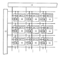
図2に画素アレイの第m列、第n行乃至第n+2行(m、nは1以上の自然数)における画素10の具体例を示す。
FIG. 2 shows a specific example of the pixels 10 in the m-th column, the n-th row to the (n + 2) -th row (m and n are natural numbers of 1 or more) of the pixel array.
画素10は、トランジスタ101と、トランジスタ102と、トランジスタ103と、トランジスタ104と、容量素子105と、容量素子106と、回路ブロック110を有する構成とすることができる。回路ブロック110は、トランジスタ、容量素子、および表示素子などを有することができ、詳細は後述する。
The pixel 10 can include a transistor 101, a transistor 102, a transistor 103, a transistor 104, a capacitor 105, a capacitor 106, and a circuit block 110. The circuit block 110 can include a transistor, a capacitor, a display element, and the like, which will be described in detail later.
トランジスタ101のソースまたはドレインの一方は、容量素子105の一方の電極と電気的に接続される。容量素子105の一方の電極は、トランジスタ102のソースまたはドレインの一方と電気的に接続される。トランジスタ102のソースまたはドレインの他方は、トランジスタ103のソースまたはドレインの一方と電気的に接続される。トランジスタ103のソースまたはドレインの一方は、容量素子106の一方の電極と電気的に接続される。容量素子106の他方の電極は、トランジスタ104のソースまたはドレインの一方と電気的に接続される。トランジスタ104のソースまたはドレインの一方は、回路ブロック110と電気的に接続される。
One of a source and a drain of the transistor 101 is electrically connected to one electrode of the capacitor 105. One electrode of the capacitor 105 is electrically connected to one of a source and a drain of the transistor 102. The other of the source and the drain of the transistor 102 is electrically connected to one of the source and the drain of the transistor 103. One of a source and a drain of the transistor 103 is electrically connected to one electrode of the capacitor 106. The other electrode of the capacitor 106 is electrically connected to one of a source and a drain of the transistor 104. One of a source and a drain of the transistor 104 is electrically connected to the circuit block 110.
ここで、トランジスタ104のソースまたはドレインの一方、容量素子106の他方の電極、および回路ブロックが接続される配線をノードNMとする。回路ブロック110が有する表示素子は、ノードNMの電位に従って動作する。なお、ノードNMと接続する回路ブロック110の要素は、ノードNMをフローティングにすることができる。
Here, a wiring to which one of the source and the drain of the transistor 104, the other electrode of the capacitor 106, and the circuit block are connected is a node NM. The display element included in the circuit block 110 operates according to the potential of the node NM. The element of the circuit block 110 connected to the node NM can make the node NM floating.
また、トランジスタ101のソースまたはドレインの一方、容量素子105の一方の電極、およびトランジスタ102のソースまたはドレインの一方が接続される配線をノードNAとする。また、トランジスタ102のソースまたはドレインの他方、容量素子106の一方の電極、およびトランジスタ103のソースまたはドレインの一方が接続される配線をノードNBとする。
A wiring to which one of the source and the drain of the transistor 101, one electrode of the capacitor 105, and one of the source and the drain of the transistor 102 are connected is a node NA. A wiring to which the other of the source and the drain of the transistor 102, one electrode of the capacitor 106, and one of the source and the drain of the transistor 103 are connected is a node NB.
なお、図1における記憶部M1は、ノードNMおよびその周辺要素に相当する。また、図1における記憶部M2は、ノードNAおよびその周辺要素に相当する。また、図1における表示素子11は、回路ブロック110が有する一要素である。
Note that the storage unit M1 in FIG. 1 corresponds to the node NM and its peripheral elements. Further, the storage unit M2 in FIG. 1 corresponds to the node NA and its peripheral elements. Further, the display element 11 in FIG. 1 is one element included in the circuit block 110.
第n行目の画素10[n,m]において、トランジスタ101のゲート、トランジスタ103のゲートおよびトランジスタ104のゲートは、配線121[n]と電気的に接続される。トランジスタ102のゲートは、配線121[n+1]と電気的に接続される。トランジスタ101のソースまたはドレインの他方およびトランジスタ104のソースまたはドレインの他方は、配線125[m]と電気的に接続される。トランジスタ103のソースまたはドレインの他方は、特定の電位“Vref”を供給することのできる配線と電気的に接続される。容量素子105の他方の電極は、特定の電位“Vr”を供給することのできる配線と電気的に接続される。
In the pixel 10 [n, m] in the n-th row, the gate of the transistor 101, the gate of the transistor 103, and the gate of the transistor 104 are electrically connected to the wiring 121 [n]. A gate of the transistor 102 is electrically connected to the wiring 121 [n + 1]. The other of the source and the drain of the transistor 101 and the other of the source and the drain of the transistor 104 are electrically connected to the wiring 125 [m]. The other of the source and the drain of the transistor 103 is electrically connected to a wiring that can supply a specific potential “V ref ”. The other electrode of the capacitor 105 is electrically connected to a wiring that can supply a specific potential “V r ”.
また、第n+1行目の画素10[n+1,m]において、トランジスタ101のゲート、トランジスタ103のゲートおよびトランジスタ104のゲートは、配線121[n+1]と電気的に接続される。トランジスタ102のゲートは、配線121[n+2]と電気的に接続される。トランジスタ101のソースまたはドレインの他方およびトランジスタ104のソースまたはドレインの他方は、配線125[m]と電気的に接続される。トランジスタ103のソースまたはドレインの他方は、特定の電位“Vref”を供給することのできる配線と電気的に接続される。容量素子105の他方の電極は、特定の電位“Vr”を供給することのできる配線と電気的に接続される。
In the pixel 10 [n + 1, m] in the (n + 1) th row, the gate of the transistor 101, the gate of the transistor 103, and the gate of the transistor 104 are electrically connected to the wiring 121 [n + 1]. A gate of the transistor 102 is electrically connected to the wiring 121 [n + 2]. The other of the source and the drain of the transistor 101 and the other of the source and the drain of the transistor 104 are electrically connected to the wiring 125 [m]. The other of the source and the drain of the transistor 103 is electrically connected to a wiring that can supply a specific potential “V ref ”. The other electrode of the capacitor 105 is electrically connected to a wiring that can supply a specific potential “V r ”.
配線121はゲート線としての機能を有し、ゲートドライバ13(図1参照)と電気的に接続される。配線125はソース線としての機能を有し、ソースドライバ12(図1参照)と電気的に接続される。
The wiring 121 functions as a gate line and is electrically connected to the gate driver 13 (see FIG. 1). The wiring 125 functions as a source line and is electrically connected to the source driver 12 (see FIG. 1).
上述したように、ゲート線(配線121)は、垂直方向において隣接する二つの画素10と電気的に接続する。したがって、垂直方向の二つの画素10の並列動作が可能となる。
As described above, the gate line (wiring 121) is electrically connected to two adjacent pixels 10 in the vertical direction. Therefore, the two pixels 10 in the vertical direction can be operated in parallel.
“Vref”および“Vr”を供給することのできる配線としては、例えば回路ブロック110の要素と電気的に接続される電源線などを用いることができる。なお、“Vref”および“Vr”を供給することのできる配線は同一であってもよいし、異なっていてもよい。
As a wiring that can supply “V ref ” and “V r ”, for example, a power supply line that is electrically connected to an element of the circuit block 110 can be used. Note that the wirings that can supply “V ref ” and “V r ” may be the same or different.
ノードNM、ノードNAおよびノードNBは、記憶ノードとして作用する。各ノードに接続するトランジスタを導通させることで、データを各ノードに書き込むことができる。また、当該トランジスタを非導通とすることで、当該データを各ノードに保持することができる。当該トランジスタに極めてオフ電流の低いトランジスタを用いることでリーク電流を抑えることができ、各ノードの電位を長時間保持することが可能となる。当該トランジスタには、例えば、金属酸化物をチャネル形成領域に用いたトランジスタ(以下、OSトランジスタ)を用いることができる。
Node NM, node NA and node NB act as storage nodes. By turning on a transistor connected to each node, data can be written to each node. Further, when the transistor is off, the data can be held in each node. By using a transistor with extremely low off-state current as the transistor, leakage current can be suppressed and the potential of each node can be held for a long time. As the transistor, for example, a transistor using a metal oxide for a channel formation region (hereinafter referred to as an OS transistor) can be used.
具体的には、トランジスタ101、102、103、104にOSトランジスタを適用することが好ましい。また、回路ブロック110が有する要素にOSトランジスタを適用してもよい。また、リーク電流量が許容できる範囲で動作を行う場合は、Siをチャネル形成領域に有するトランジスタ(以下、Siトランジスタ)を適用してもよい。または、OSトランジスタおよびSiトランジスタを併用してもよい。なお、上記Siトランジスタとしては、アモルファスシリコンを有するトランジスタ、結晶性のシリコン(代表的には、低温ポリシリコン、単結晶シリコン)を有するトランジスタなどが挙げられる。
Specifically, an OS transistor is preferably used as the transistors 101, 102, 103, and 104. Further, an OS transistor may be applied to an element included in the circuit block 110. In addition, in the case where the operation is performed in a range in which the amount of leakage current is allowable, a transistor having Si in a channel formation region (hereinafter referred to as Si transistor) may be applied. Alternatively, an OS transistor and a Si transistor may be used in combination. Note that examples of the Si transistor include a transistor including amorphous silicon and a transistor including crystalline silicon (typically, low-temperature polysilicon or single crystal silicon).
OSトランジスタに用いる半導体材料としては、エネルギーギャップが2eV以上、好ましくは2.5eV以上、より好ましくは3eV以上である金属酸化物を用いることができる。代表的には、インジウムを含む酸化物半導体などであり、例えば、後述するCAAC−OS(C−Axis Aligned Crystalline Oxide Semiconductor)またはCAC(Cloud−Aligned Composite)−OSなどを用いることができる。CAAC−OSは結晶を構成する原子が安定であり、信頼性を重視するトランジスタなどに適する。また、CAC−OSは、高移動度特性を示すため、高速駆動を行うトランジスタなどに適する。
As a semiconductor material used for the OS transistor, a metal oxide having an energy gap of 2 eV or more, preferably 2.5 eV or more, more preferably 3 eV or more can be used. Typically, the oxide semiconductor includes indium, for example, a CAAC-OS (C-Axis Crystalline Oxide Semiconductor) or a CAC (Cloud-Aligned Composite) -OS described later can be used. A CAAC-OS is suitable for a transistor or the like in which atoms constituting a crystal are stable and reliability is important. In addition, since the CAC-OS exhibits high mobility characteristics, it is suitable for a transistor that performs high-speed driving.
OSトランジスタはエネルギーギャップが大きいため、数yA/μm(チャネル幅1μmあたりの電流値)という極めて低いオフ電流特性を示す。また、OSトランジスタは、インパクトイオン化、アバランシェ降伏、および短チャネル効果などが生じないなどSiトランジスタとは異なる特徴を有し、信頼性の高い回路を形成することができる。また、Siトランジスタでは問題となる結晶性の不均一性に起因する電気特性のばらつきもOSトランジスタでは生じにくい。
Since the OS transistor has a large energy gap, it exhibits extremely low off-current characteristics of several yA / μm (current value per channel width of 1 μm). Further, the OS transistor has characteristics different from those of the Si transistor such that impact ionization, avalanche breakdown, a short channel effect, and the like do not occur, and a highly reliable circuit can be formed. In addition, variations in electrical characteristics due to non-uniformity of crystallinity, which is a problem in Si transistors, are less likely to occur in OS transistors.
OSトランジスタが有する半導体層は、例えばインジウム、亜鉛およびM(アルミニウム、チタン、ガリウム、ゲルマニウム、イットリウム、ジルコニウム、ランタン、セリウム、スズ、ネオジムまたはハフニウム等の金属)を含むIn−M−Zn系酸化物で表記される膜とすることができる。
The semiconductor layer included in the OS transistor includes, for example, an In-M-Zn-based oxide containing indium, zinc, and M (a metal such as aluminum, titanium, gallium, germanium, yttrium, zirconium, lanthanum, cerium, tin, neodymium, or hafnium). It can be set as the film | membrane described by.
半導体層を構成する酸化物半導体がIn−M−Zn系酸化物の場合、In−M−Zn酸化物を成膜するために用いるスパッタリングターゲットの金属元素の原子数比は、In≧M、Zn≧Mを満たすことが好ましい。このようなスパッタリングターゲットの金属元素の原子数比として、In:M:Zn=1:1:1、In:M:Zn=1:1:1.2、In:M:Zn=3:1:2、In:M:Zn=4:2:3、In:M:Zn=4:2:4.1、In:M:Zn=5:1:6、In:M:Zn=5:1:7、In:M:Zn=5:1:8等が好ましい。なお、成膜される半導体層の原子数比はそれぞれ、上記のスパッタリングターゲットに含まれる金属元素の原子数比のプラスマイナス40%の変動を含む。
In the case where the oxide semiconductor included in the semiconductor layer is an In-M-Zn-based oxide, the atomic ratio of the metal elements of the sputtering target used for forming the In-M-Zn oxide is In ≧ M, Zn It is preferable to satisfy ≧ M. As the atomic ratio of the metal elements of such a sputtering target, In: M: Zn = 1: 1: 1, In: M: Zn = 1: 1: 1.2, In: M: Zn = 3: 1: 2, In: M: Zn = 4: 2: 3, In: M: Zn = 4: 2: 4.1, In: M: Zn = 5: 1: 6, In: M: Zn = 5: 1: 7, In: M: Zn = 5: 1: 8 etc. are preferable. Note that the atomic ratio of the semiconductor layer to be formed includes a variation of plus or minus 40% of the atomic ratio of the metal element contained in the sputtering target.
半導体層としては、キャリア密度の低い酸化物半導体を用いる。例えば、半導体層は、キャリア密度が1×10¹⁷/cm3以下、好ましくは1×1015/cm3以下、さらに好ましくは1×1013/cm3以下、より好ましくは1×1011/cm3以下、さらに好ましくは1×1010/cm3未満であり、1×10−9/cm3以上のキャリア密度の酸化物半導体を用いることができる。そのような酸化物半導体を、高純度真性または実質的に高純度真性な酸化物半導体と呼ぶ。当該酸化物半導体は欠陥準位密度が低く、安定な特性を有する酸化物半導体であるといえる。
As the semiconductor layer, an oxide semiconductor with low carrier density is used. For example, the semiconductor layer has a carrier density of 1 × 10 17 / cm 3 or less, preferably 1 × 10 15 / cm 3 or less, more preferably 1 × 10 13 / cm 3 or less, more preferably 1 × 10 11 / cm 3. 3 or less, more preferably less than 1 × 10 10 / cm 3 , and an oxide semiconductor having a carrier density of 1 × 10 −9 / cm 3 or more can be used. Such an oxide semiconductor is referred to as a highly purified intrinsic or substantially highly purified intrinsic oxide semiconductor. It can be said that the oxide semiconductor is an oxide semiconductor having a low density of defect states and stable characteristics.
なお、これらに限られず、必要とするトランジスタの半導体特性および電気特性(電界効果移動度、しきい値電圧等)に応じて適切な組成のものを用いればよい。また、必要とするトランジスタの半導体特性を得るために、半導体層のキャリア密度や不純物濃度、欠陥密度、金属元素と酸素の原子数比、原子間距離、密度等を適切なものとすることが好ましい。
Note that the composition is not limited thereto, and a transistor having an appropriate composition may be used depending on required semiconductor characteristics and electrical characteristics (such as field-effect mobility and threshold voltage) of the transistor. In addition, in order to obtain the required semiconductor characteristics of the transistor, it is preferable that the semiconductor layer have appropriate carrier density, impurity concentration, defect density, atomic ratio of metal element to oxygen, interatomic distance, density, and the like. .
半導体層を構成する酸化物半導体において、第14族元素の一つであるシリコンや炭素が含まれると、酸素欠損が増加し、n型化してしまう。このため、半導体層におけるシリコンや炭素の濃度(二次イオン質量分析法(SIMS:Secondary Ion Mass Spectrometry)により得られる濃度)を、2×10¹⁸atoms/cm3以下、好ましくは2×1017atoms/cm3以下とする。
In the oxide semiconductor constituting the semiconductor layer, when silicon or carbon, which is one of Group 14 elements, is included, oxygen deficiency increases and the n-type semiconductor is formed. Therefore, the concentration of silicon or carbon in the semiconductor layer (concentration obtained by secondary ion mass spectrometry (SIMS)) is 2 × 10 18 atoms / cm 3 or less, preferably 2 × 10 17 atoms. / Cm 3 or less.
また、アルカリ金属およびアルカリ土類金属は、酸化物半導体と結合するとキャリアを生成する場合があり、トランジスタのオフ電流が増大してしまうことがある。このため、半導体層におけるアルカリ金属またはアルカリ土類金属の濃度(SIMSにより得られる濃度)を、1×10¹⁸atoms/cm3以下、好ましくは2×1016atoms/cm3以下にする。
Further, when alkali metal and alkaline earth metal are combined with an oxide semiconductor, carriers may be generated, which may increase off-state current of the transistor. Therefore, the concentration of alkali metal or alkaline earth metal (concentration obtained by SIMS) in the semiconductor layer is set to 1 × 10 18 atoms / cm 3 or less, preferably 2 × 10 16 atoms / cm 3 or less.
また、半導体層を構成する酸化物半導体に窒素が含まれていると、キャリアである電子が生じてキャリア密度が増加し、n型化しやすい。この結果、窒素が含まれている酸化物半導体を用いたトランジスタはノーマリーオン特性となりやすい。このため半導体層における窒素濃度(SIMSにより得られる濃度)は、5×10¹⁸atoms/cm3以下にすることが好ましい。
In addition, when nitrogen is contained in the oxide semiconductor included in the semiconductor layer, electrons as carriers are generated, the carrier density is increased, and the oxide semiconductor is easily n-type. As a result, a transistor including an oxide semiconductor containing nitrogen is likely to be normally on. For this reason, it is preferable that the nitrogen concentration (concentration obtained by SIMS) in the semiconductor layer is 5 × 10 18 atoms / cm 3 or less.
また、半導体層を構成する酸化物半導体に水素が含まれていると、金属原子と結合する酸素と反応して水になるため、酸化物半導体中に酸素欠損を形成する場合がある。酸化物半導体中のチャネル形成領域に酸素欠損が含まれていると、トランジスタはノーマリーオン特性となる場合がある。さらに、酸素欠損に水素が入った欠陥はドナーとして機能し、キャリアである電子が生成されることがある。また、水素の一部が金属原子と結合する酸素と結合して、キャリアである電子を生成する場合がある。したがって、水素が多く含まれている酸化物半導体を用いたトランジスタは、ノーマリーオン特性となりやすい。
In addition, when hydrogen is contained in the oxide semiconductor included in the semiconductor layer, oxygen reacts with oxygen bonded to a metal atom to be water, so that an oxygen vacancy may be formed in the oxide semiconductor. When an oxygen vacancy is included in a channel formation region in the oxide semiconductor, the transistor may be normally on. Furthermore, a defect in which hydrogen is contained in an oxygen vacancy functions as a donor, and electrons as carriers may be generated. In some cases, part of hydrogen is combined with oxygen bonded to a metal atom to generate electrons as carriers. Therefore, a transistor including an oxide semiconductor containing a large amount of hydrogen is likely to be normally on.
酸素欠損に水素が入った欠陥は、酸化物半導体のドナーとして機能しうる。しかしながら、当該欠陥を定量的に評価することは困難である。そこで、酸化物半導体においては、ドナー濃度ではなく、キャリア濃度で評価される場合がある。よって、本明細書等では、酸化物半導体のパラメータとして、ドナー濃度ではなく、電界が印加されない状態を想定したキャリア濃度を用いる場合がある。つまり、本明細書等に記載の「キャリア濃度」は、「ドナー濃度」と言い換えることができる場合がある。
A defect in which hydrogen is contained in an oxygen vacancy can function as a donor of an oxide semiconductor. However, it is difficult to quantitatively evaluate the defect. Thus, an oxide semiconductor may be evaluated using a carrier concentration instead of a donor concentration. Therefore, in this specification and the like, as a parameter of an oxide semiconductor, a carrier concentration that assumes a state where an electric field is not applied may be used instead of a donor concentration. That is, the “carrier concentration” described in this specification and the like can be referred to as “donor concentration” in some cases.
よって、酸化物半導体中の水素はできる限り低減されていることが好ましい。具体的には、酸化物半導体において、SIMSにより得られる水素濃度を、1×10²⁰atoms/cm3未満、好ましくは1×1019atoms/cm3未満、より好ましくは5×1018atoms/cm3未満、さらに好ましくは1×1018atoms/cm3未満とする。水素などの不純物が十分に低減された酸化物半導体をトランジスタのチャネル形成領域に用いることで、安定した電気特性を付与することができる。
Therefore, hydrogen in the oxide semiconductor is preferably reduced as much as possible. Specifically, in an oxide semiconductor, the hydrogen concentration obtained by SIMS is less than 1 × 10 20 atoms / cm 3 , preferably less than 1 × 10 19 atoms / cm 3 , more preferably 5 × 10 18 atoms / cm 3. Less than 3 , more preferably less than 1 × 10 18 atoms / cm 3 . By using an oxide semiconductor in which impurities such as hydrogen are sufficiently reduced for a channel formation region of a transistor, stable electrical characteristics can be imparted.
また、半導体層は、例えば非単結晶構造でもよい。非単結晶構造は、例えば、c軸に配向した結晶を有するCAAC−OS、多結晶構造、微結晶構造、または非晶質構造を含む。非単結晶構造において、非晶質構造は最も欠陥準位密度が高く、CAAC−OSは最も欠陥準位密度が低い。
The semiconductor layer may have a non-single crystal structure, for example. The non-single-crystal structure includes, for example, a CAAC-OS having a crystal oriented in the c-axis, a polycrystalline structure, a microcrystalline structure, or an amorphous structure. In the non-single-crystal structure, the amorphous structure has the highest density of defect states, and the CAAC-OS has the lowest density of defect states.
非晶質構造の酸化物半導体膜は、例えば、原子配列が無秩序であり、結晶成分を有さない。または、非晶質構造の酸化物膜は、例えば、完全な非晶質構造であり、結晶部を有さない。
An oxide semiconductor film having an amorphous structure has, for example, disordered atomic arrangement and no crystal component. Alternatively, an amorphous oxide film has, for example, a completely amorphous structure and does not have a crystal part.
なお、半導体層が、非晶質構造の領域、微結晶構造の領域、多結晶構造の領域、CAAC−OSの領域、単結晶構造の領域のうち、二種以上を有する混合膜であってもよい。混合膜は、例えば上述した領域のうち、いずれか二種以上の領域を含む単層構造、または積層構造を有する場合がある。
Note that the semiconductor layer may be a mixed film including two or more of an amorphous structure region, a microcrystalline structure region, a polycrystalline structure region, a CAAC-OS region, and a single crystal structure region. Good. For example, the mixed film may have a single-layer structure or a stacked structure including any two or more of the above-described regions.
以下では、非単結晶の半導体層の一態様であるCAC−OSの構成について説明する。
A structure of a CAC-OS that is one embodiment of a non-single-crystal semiconductor layer is described below.
CAC−OSとは、例えば、酸化物半導体を構成する元素が、0.5nm以上10nm以下、好ましくは、1nm以上2nm以下、またはその近傍のサイズで偏在した材料の一構成である。なお、以下では、酸化物半導体において、一つあるいはそれ以上の金属元素が偏在し、該金属元素を有する領域が、0.5nm以上10nm以下、好ましくは、1nm以上2nm以下、またはその近傍のサイズで混合した状態をモザイク状、またはパッチ状ともいう。
The CAC-OS is one structure of a material in which an element included in an oxide semiconductor is unevenly distributed with a size of 0.5 nm to 10 nm, preferably 1 nm to 2 nm, or the vicinity thereof. Note that in the following, in an oxide semiconductor, one or more metal elements are unevenly distributed, and a region including the metal element has a size of 0.5 nm to 10 nm, preferably 1 nm to 2 nm, or the vicinity thereof. The state mixed with is also referred to as a mosaic or patch.
なお、酸化物半導体は、少なくともインジウムを含むことが好ましい。特にインジウムおよび亜鉛を含むことが好ましい。また、それらに加えて、アルミニウム、ガリウム、イットリウム、銅、バナジウム、ベリリウム、ホウ素、シリコン、チタン、鉄、ニッケル、ゲルマニウム、ジルコニウム、モリブデン、ランタン、セリウム、ネオジム、ハフニウム、タンタル、タングステン、またはマグネシウムなどから選ばれた一種、または複数種が含まれていてもよい。
Note that the oxide semiconductor preferably contains at least indium. In particular, it is preferable to contain indium and zinc. In addition, aluminum, gallium, yttrium, copper, vanadium, beryllium, boron, silicon, titanium, iron, nickel, germanium, zirconium, molybdenum, lanthanum, cerium, neodymium, hafnium, tantalum, tungsten, magnesium, etc. One kind selected from the above or a plurality of kinds may be included.
例えば、In−Ga−Zn酸化物におけるCAC−OS(CAC−OSの中でもIn−Ga−Zn酸化物を、特にCAC−IGZOと呼称してもよい。)とは、インジウム酸化物(以下、InOX1(X1は0よりも大きい実数)とする。)、またはインジウム亜鉛酸化物(以下、InX2ZnY2OZ2(X2、Y2、およびZ2は0よりも大きい実数)とする。)と、ガリウム酸化物(以下、GaOX3(X3は0よりも大きい実数)とする。)、またはガリウム亜鉛酸化物(以下、GaX4ZnY4OZ4(X4、Y4、およびZ4は0よりも大きい実数)とする。)などと、に材料が分離することでモザイク状となり、モザイク状のInOX1、またはInX2ZnY2OZ2が、膜中に均一に分布した構成(以下、クラウド状ともいう。)である。
For example, a CAC-OS in In-Ga-Zn oxide (In-Ga-Zn oxide among CAC-OSs may be referred to as CAC-IGZO in particular) is an indium oxide (hereinafter referred to as InO). X1 (X1 is greater real than 0) and.), or indium zinc oxide (hereinafter, in X2 Zn Y2 O Z2 ( X2, Y2, and Z2 is larger real than 0) and a.), gallium An oxide (hereinafter referred to as GaO X3 (X3 is a real number greater than 0)) or a gallium zinc oxide (hereinafter referred to as Ga X4 Zn Y4 O Z4 (where X4, Y4, and Z4 are greater than 0)) to.) and the like, the material becomes mosaic by separate into, mosaic InO X1 or in X2 Zn Y2 O Z2, is a configuration in which uniformly distributed in the film (hereinafter Also referred to as a cloud-like.) A.
つまり、CAC−OSは、GaOX3が主成分である領域と、InX2ZnY2OZ2、またはInOX1が主成分である領域とが、混合している構成を有する複合酸化物半導体である。なお、本明細書において、例えば、第1の領域の元素Mに対するInの原子数比が、第2の領域の元素Mに対するInの原子数比よりも大きいことを、第1の領域は、第2の領域と比較して、Inの濃度が高いとする。
That, CAC-OS includes a region GaO X3 is the main component, and In X2 Zn Y2 O Z2, or InO X1 is the main component region is a composite oxide semiconductor having a structure that is mixed. Note that in this specification, for example, the first region indicates that the atomic ratio of In to the element M in the first region is larger than the atomic ratio of In to the element M in the second region. It is assumed that the concentration of In is higher than that in the second region.
なお、IGZOは通称であり、In、Ga、Zn、およびOによる1つの化合物をいう場合がある。代表例として、InGaO3(ZnO)m1(m1は自然数)、またはIn(1+x0)Ga(1−x0)O3(ZnO)m0(−1≦x0≦1、m0は任意数)で表される結晶性の化合物が挙げられる。
Note that IGZO is a common name and may refer to one compound of In, Ga, Zn, and O. As a typical example, InGaO 3 (ZnO) m1 (m1 is a natural number) or In (1 + x0) Ga (1-x0) O 3 (ZnO) m0 (−1 ≦ x0 ≦ 1, m0 is an arbitrary number) A crystalline compound may be mentioned.
上記結晶性の化合物は、単結晶構造、多結晶構造、またはCAAC構造を有する。なお、CAAC構造とは、複数のIGZOのナノ結晶がc軸配向を有し、かつa−b面においては配向せずに連結した結晶構造である。
The crystalline compound has a single crystal structure, a polycrystalline structure, or a CAAC structure. The CAAC structure is a crystal structure in which a plurality of IGZO nanocrystals have c-axis orientation and are connected without being oriented in the ab plane.
一方、CAC−OSは、酸化物半導体の材料構成に関する。CAC−OSとは、In、Ga、Zn、およびOを含む材料構成において、一部にGaを主成分とするナノ粒子状に観察される領域と、一部にInを主成分とするナノ粒子状に観察される領域とが、それぞれモザイク状にランダムに分散している構成をいう。したがって、CAC−OSにおいて、結晶構造は副次的な要素である。
On the other hand, CAC-OS relates to a material structure of an oxide semiconductor. CAC-OS refers to a region observed in the form of nanoparticles mainly composed of Ga in a material structure including In, Ga, Zn and O, and nanoparticles mainly composed of In. The region observed in a shape is a configuration in which the regions are randomly dispersed in a mosaic shape. Therefore, in the CAC-OS, the crystal structure is a secondary element.
なお、CAC−OSは、組成の異なる二種類以上の膜の積層構造は含まないものとする。例えば、Inを主成分とする膜と、Gaを主成分とする膜との2層からなる構造は、含まない。
Note that the CAC-OS does not include a stacked structure of two or more kinds of films having different compositions. For example, a structure composed of two layers of a film mainly containing In and a film mainly containing Ga is not included.
なお、GaOX3が主成分である領域と、InX2ZnY2OZ2、またはInOX1が主成分である領域とは、明確な境界が観察できない場合がある。
Incidentally, a region GaO X3 is the main component, and In X2 Zn Y2 O Z2 or InO X1 is the main component region, in some cases clear boundary can not be observed.
なお、ガリウムの代わりに、アルミニウム、イットリウム、銅、バナジウム、ベリリウム、ホウ素、シリコン、チタン、鉄、ニッケル、ゲルマニウム、ジルコニウム、モリブデン、ランタン、セリウム、ネオジム、ハフニウム、タンタル、タングステン、またはマグネシウムなどから選ばれた一種、または複数種が含まれている場合、CAC−OSは、一部に該金属元素を主成分とするナノ粒子状に観察される領域と、一部にInを主成分とするナノ粒子状に観察される領域とが、それぞれモザイク状にランダムに分散している構成をいう。
Instead of gallium, selected from aluminum, yttrium, copper, vanadium, beryllium, boron, silicon, titanium, iron, nickel, germanium, zirconium, molybdenum, lanthanum, cerium, neodymium, hafnium, tantalum, tungsten, magnesium, etc. In the case where one or a plurality of types are included, the CAC-OS includes a region that is observed in a part of a nanoparticle mainly including the metal element and a nanoparticle mainly including In. The region observed in the form of particles refers to a configuration in which each region is randomly dispersed in a mosaic shape.
CAC−OSは、例えば基板を意図的に加熱しない条件で、スパッタリング法により形成することができる。また、CAC−OSをスパッタリング法で形成する場合、成膜ガスとして、不活性ガス(代表的にはアルゴン)、酸素ガス、および窒素ガスの中から選ばれたいずれか一つまたは複数を用いればよい。また、成膜時の成膜ガスの総流量に対する酸素ガスの流量比は低いほど好ましく、例えば酸素ガスの流量比を0%以上30%未満、好ましくは0%以上10%以下とすることが好ましい。
The CAC-OS can be formed by a sputtering method under a condition where the substrate is not intentionally heated, for example. In the case where a CAC-OS is formed by a sputtering method, any one or more selected from an inert gas (typically argon), an oxygen gas, and a nitrogen gas may be used as a deposition gas. Good. Further, the flow rate ratio of the oxygen gas to the total flow rate of the deposition gas during film formation is preferably as low as possible. For example, the flow rate ratio of the oxygen gas is 0% or more and less than 30%, preferably 0% or more and 10% or less. .
CAC−OSは、X線回折(XRD:X−ray diffraction)測定法のひとつであるOut−of−plane法によるθ/2θスキャンを用いて測定したときに、明確なピークが観察されないという特徴を有する。すなわち、X線回折測定から、測定領域のa−b面方向、およびc軸方向の配向は見られないことが分かる。
The CAC-OS has a feature that a clear peak is not observed when measurement is performed using a θ / 2θ scan by an out-of-plane method, which is one of X-ray diffraction (XRD) measurement methods. Have. That is, from the X-ray diffraction measurement, it is understood that no orientation in the ab plane direction and c-axis direction of the measurement region is observed.
また、CAC−OSは、プローブ径が1nmの電子線(ナノビーム電子線ともいう。)を照射することで得られる電子線回折パターンにおいて、リング状に輝度の高い領域(リング領域)と、該リング領域に複数の輝点が観測される。したがって、電子線回折パターンから、CAC−OSの結晶構造が、平面方向、および断面方向において、配向性を有さないnc(nanocrystalline)構造を有することがわかる。
In addition, a CAC-OS includes a ring-shaped region having a high luminance (ring region) in an electron beam diffraction pattern obtained by irradiating an electron beam having a probe diameter of 1 nm (also referred to as a nanobeam electron beam), the ring Multiple bright spots are observed in the region. Therefore, it can be seen from the electron beam diffraction pattern that the crystal structure of the CAC-OS has an nc (nanocrystalline) structure having no orientation in the planar direction and the cross-sectional direction.
また、例えば、In−Ga−Zn酸化物におけるCAC−OSでは、エネルギー分散型X線分光法(EDX:Energy Dispersive X−ray spectroscopy)を用いて取得したEDXマッピングにより、GaOX3が主成分である領域と、InX2ZnY2OZ2、またはInOX1が主成分である領域とが、偏在し、混合している構造を有することが確認できる。
In addition, for example, in a CAC-OS in an In—Ga—Zn oxide, GaO X3 is a main component by EDX mapping obtained by using energy dispersive X-ray spectroscopy (EDX: Energy Dispersive X-ray spectroscopy). It can be confirmed that the region and the region mainly composed of In X2 Zn Y2 O Z2 or InO X1 are unevenly distributed and mixed.
CAC−OSは、金属元素が均一に分布したIGZO化合物とは異なる構造であり、IGZO化合物と異なる性質を有する。つまり、CAC−OSは、GaOX3などが主成分である領域と、InX2ZnY2OZ2、またはInOX1が主成分である領域と、に互いに相分離し、各元素を主成分とする領域がモザイク状である構造を有する。
The CAC-OS has a structure different from that of the IGZO compound in which the metal element is uniformly distributed, and has a property different from that of the IGZO compound. That is, in the CAC-OS, a region in which GaO X3 or the like is a main component and a region in which In X2 Zn Y2 O Z2 or InO X1 is a main component are phase-separated from each other, and each region is mainly composed of each element. Has a mosaic structure.
ここで、InX2ZnY2OZ2、またはInOX1が主成分である領域は、GaOX3などが主成分である領域と比較して、導電性が高い領域である。つまり、InX2ZnY2OZ2、またはInOX1が主成分である領域を、キャリアが流れることにより、酸化物半導体としての導電性が発現する。したがって、InX2ZnY2OZ2、またはInOX1が主成分である領域が、酸化物半導体中にクラウド状に分布することで、高い電界効果移動度(μ)が実現できる。
Here, the region containing In X2 Zn Y2 O Z2 or InO X1 as a main component is a region having higher conductivity than a region containing GaO X3 or the like as a main component. That, In X2 Zn Y2 O Z2 or InO X1, is an area which is the main component, by carriers flow, expressed the conductivity of the oxide semiconductor. Therefore, a region where In X2 Zn Y2 O Z2 or InO X1 is a main component is distributed in a cloud shape in the oxide semiconductor, whereby high field-effect mobility (μ) can be realized.
一方、GaOX3などが主成分である領域は、InX2ZnY2OZ2、またはInOX1が主成分である領域と比較して、絶縁性が高い領域である。つまり、GaOX3などが主成分である領域が、酸化物半導体中に分布することで、リーク電流を抑制し、良好なスイッチング動作を実現できる。
On the other hand, areas such as GaO X3 is the main component, as compared to the In X2 Zn Y2 O Z2 or InO X1 is the main component area, it is highly regions insulating. That is, a region containing GaO X3 or the like as a main component is distributed in the oxide semiconductor, whereby leakage current can be suppressed and good switching operation can be realized.
したがって、CAC−OSを半導体素子に用いた場合、GaOX3などに起因する絶縁性と、InX2ZnY2OZ2、またはInOX1に起因する導電性とが、相補的に作用することにより、高いオン電流(Ion)、および高い電界効果移動度(μ)を実現することができる。
Therefore, when CAC-OS is used for a semiconductor element, the insulating property caused by GaO X3 and the like and the conductivity caused by In X2 Zn Y2 O Z2 or InO X1 act complementarily, thereby increasing the An on-current (I on ) and high field effect mobility (μ) can be realized.
また、CAC−OSを用いた半導体素子は、信頼性が高い。したがって、CAC−OSは、様々な半導体装置の構成材料として適している。
In addition, a semiconductor element using a CAC-OS has high reliability. Therefore, the CAC-OS is suitable as a constituent material for various semiconductor devices.
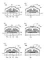
なお、画素10は、図3(A)、(B)に示す構成であってもよい。図3(A)は、トランジスタ104のソースまたはドレインの他方がトランジスタ101のソースまたはドレインの一方に接続される例である。図3(B)は、トランジスタ101のソースまたはドレインの他方がトランジスタ104のソースまたはドレインの一方に接続される例である。いずれの構成も図2の構成と同様の動作を行うことができる。
Note that the pixel 10 may have a configuration illustrated in FIGS. FIG. 3A illustrates an example in which the other of the source and the drain of the transistor 104 is connected to one of the source and the drain of the transistor 101. FIG. 3B illustrates an example in which the other of the source and the drain of the transistor 101 is connected to one of the source and the drain of the transistor 104. Either configuration can perform the same operation as the configuration of FIG.
また、画素10の加算動作では容量結合を用いるため、供給側に設けられる容量素子105の容量値を大きくすることが好ましい。一方で、画素の開口率を高めるためには、容量素子の占有面積はできるだけ小さくすることが好ましい。そのため、画素間で容量素子を互いに共有する構成としてもよい。
Further, since capacitive coupling is used in the addition operation of the pixel 10, it is preferable to increase the capacitance value of the capacitor 105 provided on the supply side. On the other hand, in order to increase the aperture ratio of the pixel, it is preferable to make the area occupied by the capacitor element as small as possible. Therefore, a structure in which a capacitor is shared between pixels may be used.
新たな書き込み動作を行っていない画素10においては、容量素子105に書き込む電位を変化させても表示動作に影響を与えない。したがって、複数の画素10で互いに容量素子105を共有し、容量値を高めることができる。なお、容量素子105を共有できる画素10は、並列動作が行われない画素10に限られる。
In the pixel 10 that has not performed a new writing operation, the display operation is not affected even if the potential written to the capacitor 105 is changed. Therefore, the capacitance element 105 can be shared by the plurality of pixels 10 to increase the capacitance value. Note that the pixels 10 that can share the capacitor 105 are limited to the pixels 10 that are not operated in parallel.
例えば、図4に示すように、接続線136を設け、垂直方向の一つ置きの画素10の容量素子105を電気的に並列接続することができる。なお、図4では2個の画素10で容量素子105を共有する構成を示したが、垂直方向の一つ置きの画素10であれば、3個以上の画素10で容量素子105を共有してもよい。
For example, as shown in FIG. 4, connection lines 136 can be provided, and the capacitor elements 105 of every other pixel 10 in the vertical direction can be electrically connected in parallel. 4 shows a configuration in which the capacitor element 105 is shared by two pixels 10, but if every other pixel 10 in the vertical direction, the capacitor element 105 is shared by three or more pixels 10. Also good.
図5に示すタイミングチャートを用いて、画素10に供給した画像データを加算する動作の一例を説明する。なお、以下の説明においては、高電位を“H”、低電位を“L”で表す。また、1行目の画素に書き込む際に供給する画像データを“D1”、2行目の画素に書き込む際に供給する画像データを“D2”、3行目の画素に書き込む際に供給する画像データを“D3”とする。”Vref”としては、例えば0V、GND電位または特定の基準電位を用いることができる。
An example of the operation of adding the image data supplied to the pixel 10 will be described using the timing chart shown in FIG. In the following description, the high potential is represented by “H” and the low potential is represented by “L”. The image data supplied when writing to the pixels in the first row is “D1”, and the image data supplied when writing to the pixels in the second row is “D2”. The data is “D3”. As “V ref ”, for example, 0 V, a GND potential, or a specific reference potential can be used.
まず、n行目の画素10[n,m]のノードNA[n,m]およびノードNM[n,m]に“D1”を書き込む動作を説明する。なお、ここでは電位の分配、結合または損失において、回路の構成や動作タイミングなどに起因する詳細な変化は勘案しない。また、容量結合による電位の変化は供給側と被供給側の容量比に依存するが、説明を明瞭にするため、回路ブロック110の容量値は十分に小さい値に仮定する。
First, an operation of writing “D1” to the node NA [n, m] and the node NM [n, m] of the pixel 10 [n, m] in the n-th row will be described. Note that detailed changes due to circuit configuration, operation timing, and the like are not taken into account in potential distribution, coupling, or loss. Further, the change in potential due to capacitive coupling depends on the capacitance ratio between the supply side and the supply side, but for the sake of clarity, the capacitance value of the circuit block 110 is assumed to be a sufficiently small value.
時刻T1に配線121[n]の電位を“H”とすると、画素10[n,m]において、トランジスタ103が導通し、容量素子106の一方の電極の電位は“Vref”となる。当該動作は、後の加算動作(容量結合動作)を行うためのリセット動作である。また、トランジスタ101が導通し、ノードNA[n,m]に配線125[m]の電位が書き込まれる。また、トランジスタ104が導通し、ノードNM[n,m]に配線125[m]の電位が書き込まれる。当該動作は画像データの書き込み動作であり、ノードNA[n,m]およびノードNM[n,m]の電位は“D1”となる。
When the potential of the wiring 121 [n] is set to “H” at time T1, the transistor 103 is turned on in the pixel 10 [n, m], and the potential of one electrode of the capacitor 106 becomes “V ref ”. This operation is a reset operation for performing a later addition operation (capacitive coupling operation). In addition, the transistor 101 is turned on, and the potential of the wiring 125 [m] is written to the node NA [n, m]. In addition, the transistor 104 is turned on, and the potential of the wiring 125 [m] is written to the node NM [n, m]. This operation is an image data writing operation, and the potentials of the node NA [n, m] and the node NM [n, m] are “D1”.
時刻T2に配線121[n]の電位を“L”とすると、トランジスタ101、トランジスタ103およびトランジスタ104が非導通となる。このとき、ノードNA[n,m]およびノードNM[n,m]に“D1”が保持される。また、容量素子106には、“D1−Vref”が保持される。
When the potential of the wiring 121 [n] is set to “L” at time T2, the transistor 101, the transistor 103, and the transistor 104 are turned off. At this time, “D1” is held in the node NA [n, m] and the node NM [n, m]. Further, “D 1 −V ref ” is held in the capacitor 106.
ここまでが画素10[n,m]における“D1”の書き込み動作である。次に画素10[n,m]における“D1”の加算動作および画素10[n+1,m]における“D2”の書き込み動作を説明する。
The operation so far is the writing operation of “D1” in the pixel 10 [n, m]. Next, the operation of adding “D1” in the pixel 10 [n, m] and the operation of writing “D2” in the pixel 10 [n + 1, m] will be described.
時刻T2に配線121[n+1]の電位を“H”とすると、画素10[n,m]において、トランジスタ102が導通し、ノードNA[n,m]に保持された“D1”がノードNB[n,m]に読み出される。このとき、容量素子106の容量結合によりノードNM[n,m]の電位にノードNB[n,m]の電位“D1”が付加される。当該動作は加算動作であり、ノードNM[n,m]の電位は“D1−Vref+D1”となる。このとき、“Vref”=0であれば、ノードNM[n,m]の電位は、“D1+D1”となる。すなわち、はじめにノードNA[n,m]およびノードNM[n,m]に保持されたデータを加算することができる。
When the potential of the wiring 121 [n + 1] is set to “H” at time T2, the transistor 102 is turned on in the pixel 10 [n, m], and “D1” held in the node NA [n, m] is connected to the node NB [ n, m]. At this time, the potential “D1” of the node NB [n, m] is added to the potential of the node NM [n, m] due to capacitive coupling of the capacitor 106. This operation is an addition operation, and the potential of the node NM [n, m] is “D1−V ref + D1”. At this time, if “V ref ” = 0, the potential of the node NM [n, m] is “D1 + D1”. That is, first, data held in the node NA [n, m] and the node NM [n, m] can be added.
画素10[n+1,m]においては、トランジスタ103が導通し、容量素子106の一方の電極の電位は“Vref”となる。また、トランジスタ101が導通し、ノードNA[n+1,m]に配線125[m]の電位が書き込まれる。また、トランジスタ104が導通し、ノードNM[n+1,m]に配線125[m]の電位が書き込まれる。当該動作は画像データの書き込み動作であり、ノードNA[n+1,m]およびノードNM[n+1,m]の電位は“D2”となる。
In the pixel 10 [n + 1, m], the transistor 103 is turned on, and the potential of one electrode of the capacitor 106 is “V ref ”. Further, the transistor 101 is turned on, and the potential of the wiring 125 [m] is written to the node NA [n + 1, m]. Further, the transistor 104 is turned on and the potential of the wiring 125 [m] is written to the node NM [n + 1, m]. This operation is an image data writing operation, and the potentials of the node NA [n + 1, m] and the node NM [n + 1, m] are “D2”.
ここまでが画素10[n,m]における“D1”の加算動作、および画素10[n+1,m]における“D2”の書き込み動作である。次に画素10[n+1,m]における“D2”の加算および画素10[n+2,m]における“D3”の書き込み動作を説明する。
Up to this point, the addition operation of “D1” in the pixel 10 [n, m] and the write operation of “D2” in the pixel 10 [n + 1, m] are performed. Next, the operation of adding “D2” in the pixel 10 [n + 1, m] and the writing operation of “D3” in the pixel 10 [n + 2, m] will be described.
時刻T3に配線121[n+2]の電位を“H”とすると、画素10[n+1,m]において、トランジスタ102が導通し、ノードNA[n+1,m]に保持された“D2”がノードNB[n+1,m]に読み出される。このとき、容量素子106の容量結合によりノードNM[n+1,m]の電位にノードNB[n+1,m]の電位“D2”が付加される。当該動作は加算動作であり、ノードNM[n+1,m]の電位は“D2−Vref+D2”となる。このとき、“Vref”=0であれば、ノードNM[n+1,m]の電位は、“D2+D2”となる。
When the potential of the wiring 121 [n + 2] is set to “H” at time T3, the transistor 102 is turned on in the pixel 10 [n + 1, m], and “D2” held in the node NA [n + 1, m] is connected to the node NB [ n + 1, m]. At this time, the potential “D2” of the node NB [n + 1, m] is added to the potential of the node NM [n + 1, m] due to capacitive coupling of the capacitor 106. This operation is an addition operation, and the potential of the node NM [n + 1, m] is “D2−V ref + D2”. At this time, if “V ref ” = 0, the potential of the node NM [n + 1, m] is “D2 + D2”.
画素10[n+2,m]においては、トランジスタ103が導通し、容量素子106の一方の電極の電位は“Vref”となる。また、トランジスタ101が導通し、ノードNA[n+2,m]に配線125[m]の電位が書き込まれる。また、トランジスタ104が導通し、ノードNM[n+2,m]に配線125[m]の電位が書き込まれる。当該動作は画像データの書き込み動作であり、ノードNA[n+2,m]およびノードNM[n+2,m]の電位は“D3”となる。
In the pixel 10 [n + 2, m], the transistor 103 is turned on, and the potential of one electrode of the capacitor 106 is “V ref ”. Further, the transistor 101 is turned on, and the potential of the wiring 125 [m] is written to the node NA [n + 2, m]. In addition, the transistor 104 is turned on, and the potential of the wiring 125 [m] is written to the node NM [n + 2, m]. This operation is an image data writing operation, and the potentials of the node NA [n + 2, m] and the node NM [n + 2, m] are “D3”.
ここまでが画素10[n+1,m]における“D2”の加算動作、および画素10[n+2,m]における“D3”の書き込み動作である。画素10[n+2,m]においては、図5に示すタイミングチャートに従って上述した同様の動作を行うことにより、“D3”の加算動作を行うことができる。
The operations so far are the addition operation of “D2” in the pixel 10 [n + 1, m] and the write operation of “D3” in the pixel 10 [n + 2, m]. In the pixel 10 [n + 2, m], an operation of adding “D3” can be performed by performing the same operation as described above in accordance with the timing chart shown in FIG.
以上の説明のように、本発明の一態様では2つの画像データを加算するための動作を行うことができる。画像データを加算することで、ソースドライバの最大出力電圧以上の電位を表示素子に供給することができ、表示輝度の向上やダイナミックレンジの拡大などに寄与することができる。また、標準的な表示を行う場合は、ソースドライバの出力電圧を約半分にすることもでき、消費電力を削減することもできる。
As described above, in one embodiment of the present invention, an operation for adding two pieces of image data can be performed. By adding the image data, a potential higher than the maximum output voltage of the source driver can be supplied to the display element, which can contribute to an improvement in display luminance and an expansion of the dynamic range. In addition, when performing standard display, the output voltage of the source driver can be halved, and power consumption can be reduced.
また、n行目の画素における画像データの書き込み動作とn+1行目の画素における画像データの加算動作を並行して行うことができるため、フレーム周波数を高めることができる。したがって、画素数増大によって水平期間が短い場合でもフレーム周波数を高めやすくなる。また、本発明の一態様は、高速動作が必要なフィールドシーケンシャル液晶表示装置にも適する。
In addition, since the image data writing operation in the n-th row pixel and the image data adding operation in the n + 1 row pixel can be performed in parallel, the frame frequency can be increased. Therefore, it is easy to increase the frame frequency even when the horizontal period is short due to the increase in the number of pixels. One embodiment of the present invention is also suitable for a field sequential liquid crystal display device that requires high-speed operation.
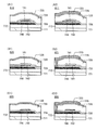
図6(A)乃至(C)は、回路ブロック110に適用でき、表示素子としてEL素子を含む構成の例である。
6A to 6C are examples of a structure which can be applied to the circuit block 110 and includes an EL element as a display element.
図6(A)に示す構成は、トランジスタ111と、容量素子113と、EL素子114を有する。トランジスタ111のソースまたはドレインの一方は、EL素子114の一方の電極と電気的に接続される。EL素子114の一方の電極は、容量素子113の一方の電極と電気的に接続される。容量素子113の他方の電極は、トランジスタ111のゲートと電気的に接続される。トランジスタ111のゲートは、ノードNMに電気的に接続される。
The structure illustrated in FIG. 6A includes a transistor 111, a capacitor 113, and an EL element 114. One of a source and a drain of the transistor 111 is electrically connected to one electrode of the EL element 114. One electrode of the EL element 114 is electrically connected to one electrode of the capacitor 113. The other electrode of the capacitor 113 is electrically connected to the gate of the transistor 111. The gate of the transistor 111 is electrically connected to the node NM.
トランジスタ111のソースまたはドレインの他方は、配線128と電気的に接続される。EL素子114の他方の電極は、配線129と電気的に接続される。配線128、129は電源を供給する機能を有する。例えば、配線128は、高電位電源を供給することができる。また、配線129は、低電位電源を供給することができる。
The other of the source and the drain of the transistor 111 is electrically connected to the wiring 128. The other electrode of the EL element 114 is electrically connected to the wiring 129. The wirings 128 and 129 have a function of supplying power. For example, the wiring 128 can supply high potential power. The wiring 129 can supply low potential power.
ここで、図1に示した“Vref”を供給するための配線には、配線128を適用することができる。また、“Vr”を供給するための配線にも配線128を適用することができる。“Vref”および“Vr”は0V、GNDまたは低電位であることが好ましいため、配線128は、少なくともそれらの電位のいずれかを供給する機能も有する。配線128には、ノードNMにデータを書き込むタイミングでは“Vref”および“Vr”を供給し、EL素子114を発光させるタイミングでは高電位電源を供給すればよい。なお、“Vref”および“Vr”を供給する専用の共通配線を設けてもよい。
Here, the wiring 128 can be applied to the wiring for supplying “V ref ” illustrated in FIG. 1. The wiring 128 can also be applied to a wiring for supplying “V r ”. Since “V ref ” and “V r ” are preferably 0 V, GND, or a low potential, the wiring 128 also has a function of supplying at least one of those potentials. The wiring 128 may be supplied with “V ref ” and “V r ” at the timing of writing data to the node NM and supplied with high potential power at the timing of causing the EL element 114 to emit light. A dedicated common wiring for supplying “V ref ” and “V r ” may be provided.
図6(A)に示す構成では、ノードNMの電位がトランジスタ111のしきい値電圧以上となったときにEL素子114に電流が流れる。したがって、図5のタイミングチャートに示す画像データの書き込みの段階でEL素子114の発光が始まる場合があり、用途が限定されることがある。
6A, current flows through the EL element 114 when the potential of the node NM becomes equal to or higher than the threshold voltage of the transistor 111. In the structure illustrated in FIG. Therefore, light emission of the EL element 114 may start at the stage of writing image data shown in the timing chart of FIG. 5, and the application may be limited.
図6(B)は、図6(A)の構成にトランジスタ112を付加した構成である。トランジスタ112のソースまたはドレインの一方は、トランジスタ111のソースまたはドレインの一方と電気的に接続される。トランジスタ112のソースまたはドレインの他方は、EL素子114と電気的に接続される。トランジスタ112のゲートは、配線127と電気的に接続される。配線127は、トランジスタ112の導通を制御する信号線としての機能を有することができる。
FIG. 6B illustrates a structure in which the transistor 112 is added to the structure in FIG. One of the source and the drain of the transistor 112 is electrically connected to one of the source and the drain of the transistor 111. The other of the source and the drain of the transistor 112 is electrically connected to the EL element 114. A gate of the transistor 112 is electrically connected to the wiring 127. The wiring 127 can function as a signal line for controlling conduction of the transistor 112.
当該構成では、ノードNMの電位がトランジスタ111のしきい値電圧以上であって、トランジスタ112が導通したときにEL素子114に電流が流れる。したがって、図3のタイミングチャートに示す2回目の書き込み以降にEL素子114の発光を開始することができる。
In this structure, current flows through the EL element 114 when the potential of the node NM is equal to or higher than the threshold voltage of the transistor 111 and the transistor 112 is turned on. Therefore, light emission of the EL element 114 can be started after the second writing shown in the timing chart of FIG.
図6(C)は、図6(B)の構成にトランジスタ115を付加した構成である。トランジスタ115のソースまたはドレインの一方は、トランジスタ111のソースまたはドレインの一方と電気的に接続される。トランジスタ115のソースまたはドレインの他方は、配線130と電気的に接続される。トランジスタ115のゲートは、配線131と電気的に接続される。配線131は、トランジスタ115の導通を制御する信号線としての機能を有することができる。
FIG. 6C illustrates a structure in which the transistor 115 is added to the structure in FIG. One of the source and the drain of the transistor 115 is electrically connected to one of the source and the drain of the transistor 111. The other of the source and the drain of the transistor 115 is electrically connected to the wiring 130. A gate of the transistor 115 is electrically connected to the wiring 131. The wiring 131 can function as a signal line for controlling conduction of the transistor 115.
配線130は、基準電位などの特定の電位の供給源と電気的に接続することができる。配線130からトランジスタ111のソースまたはドレインの一方に特定の電位を供給することで、画像データの書き込みを安定化させることもできる。
The wiring 130 can be electrically connected to a supply source of a specific potential such as a reference potential. By supplying a specific potential from the wiring 130 to one of the source and the drain of the transistor 111, writing of image data can be stabilized.
また、配線130は回路120と接続することができ、モニタ線としての機能を有することもできる。回路120は、上記特定の電位を供給する機能、トランジスタ111の電気特性を取得する機能、および補正データを生成する機能の一つ以上を有することができる。
The wiring 130 can be connected to the circuit 120 and can function as a monitor line. The circuit 120 can have one or more of a function of supplying the specific potential, a function of acquiring electrical characteristics of the transistor 111, and a function of generating correction data.
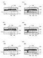
図7(A)乃至(C)は、回路ブロック110に適用でき、表示素子として液晶素子を含む構成の例である。
7A to 7C are examples of a structure which can be applied to the circuit block 110 and includes a liquid crystal element as a display element.
図7(A)に示す構成は、容量素子116および液晶素子117を有する。液晶素子117の一方の電極は、容量素子116の一方の電極と電気的に接続される。容量素子116の一方の電極は、ノードNMに電気的に接続される。
The structure illustrated in FIG. 7A includes the capacitor 116 and the liquid crystal element 117. One electrode of the liquid crystal element 117 is electrically connected to one electrode of the capacitor 116. One electrode of the capacitor 116 is electrically connected to the node NM.
容量素子116の他方の電極は、配線132と電気的に接続される。液晶素子117の他方の電極は、配線133と電気的に接続される。配線132、133は電源を供給する機能を有する。例えば、配線132、133は、GNDや0Vなどの基準電位や任意の電位を供給することができる。
The other electrode of the capacitor 116 is electrically connected to the wiring 132. The other electrode of the liquid crystal element 117 is electrically connected to the wiring 133. The wirings 132 and 133 have a function of supplying power. For example, the wirings 132 and 133 can supply a reference potential such as GND or 0 V or an arbitrary potential.
ここで、図1に示した“Vref”を供給するための配線には、配線132を適用することができる。また、“Vr”を供給するための配線にも配線132を適用することができる。なお、“Vref”および“Vr”を供給する専用の共通配線を設けてもよい。
Here, the wiring 132 can be applied to the wiring for supplying “V ref ” illustrated in FIG. 1. The wiring 132 can also be applied to a wiring for supplying “V r ”. A dedicated common wiring for supplying “V ref ” and “V r ” may be provided.
当該構成では、ノードNMの電位が液晶素子117の動作しきい値以上に確定したときに液晶素子117の動作が開始される。したがって、図5のタイミングチャートに示す画像データの書き込みの段階で表示動作が始まる場合があり、用途が限定されることがある。ただし、透過型液晶表示装置の場合は、図5のタイミングチャートに示す画像データの加算動作後までバックライトを消灯するなどの動作を併用することで、不必要な表示動作が行われても視認を抑制することができる。
In this configuration, the operation of the liquid crystal element 117 is started when the potential of the node NM is determined to be equal to or higher than the operation threshold value of the liquid crystal element 117. Accordingly, the display operation may start at the stage of writing the image data shown in the timing chart of FIG. 5, and the application may be limited. However, in the case of a transmissive liquid crystal display device, even if an unnecessary display operation is performed by using an operation such as turning off the backlight until after the image data addition operation shown in the timing chart of FIG. Can be suppressed.
図7(B)は、図7(A)の構成にトランジスタ118を付加した構成である。トランジスタ118のソースまたはドレインの一方は、容量素子116の一方の電極と電気的に接続される。トランジスタ118のソースまたはドレインの他方は、ノードNMと電気的に接続される。トランジスタ118のゲートは、配線127と電気的に接続される。配線127は、トランジスタ118の導通を制御する信号線としての機能を有することができる。
FIG. 7B illustrates a structure in which a transistor 118 is added to the structure in FIG. One of a source and a drain of the transistor 118 is electrically connected to one electrode of the capacitor 116. The other of the source and the drain of the transistor 118 is electrically connected to the node NM. A gate of the transistor 118 is electrically connected to the wiring 127. The wiring 127 can function as a signal line for controlling conduction of the transistor 118.
当該構成では、トランジスタ118の導通に伴って液晶素子117にノードNMの電位が印加される。したがって、図5に示すタイミングチャートの画像データの加算動作以降に液晶素子の動作を開始することができる。
In this structure, the potential of the node NM is applied to the liquid crystal element 117 when the transistor 118 is turned on. Therefore, the operation of the liquid crystal element can be started after the addition operation of the image data in the timing chart shown in FIG.
なお、トランジスタ118が非導通の状態では容量素子116および液晶素子117に供給された電位が保持され続けるため、画像データを書き換える前に容量素子116および液晶素子117に供給された電位をリセットすることが好ましい。当該リセットは、例えば、画素が接続されるソース線(図2に示す配線125)にリセット電位を供給し、トランジスタ103およびトランジスタ118を同時に導通させればよい。
Note that since the potential supplied to the capacitor 116 and the liquid crystal element 117 is continuously held when the transistor 118 is off, the potential supplied to the capacitor 116 and the liquid crystal element 117 is reset before rewriting image data. Is preferred. For the reset, for example, a reset potential may be supplied to the source line (the wiring 125 illustrated in FIG. 2) to which the pixel is connected, so that the transistor 103 and the transistor 118 are turned on at the same time.
図7(C)は、図7(B)の構成にトランジスタ119を付加した構成である。トランジスタ119のソースまたはドレインの一方は、液晶素子117の一方の電極と電気的に接続される。トランジスタ119のソースまたはドレインの他方は、配線130と電気的に接続される。トランジスタ119のゲートは、配線131と電気的に接続される。配線131はトランジスタ119の導通を制御する信号線としての機能を有することができる。
FIG. 7C illustrates a structure in which a transistor 119 is added to the structure in FIG. One of a source and a drain of the transistor 119 is electrically connected to one electrode of the liquid crystal element 117. The other of the source and the drain of the transistor 119 is electrically connected to the wiring 130. A gate of the transistor 119 is electrically connected to the wiring 131. The wiring 131 can function as a signal line for controlling conduction of the transistor 119.
配線130と電気的に接続される回路120は、前述した図6(C)の説明と同様であるほか、容量素子116および液晶素子117に供給された電位をリセットする機能を有していてもよい。
The circuit 120 which is electrically connected to the wiring 130 is similar to the description in FIG. 6C described above, and may have a function of resetting the potential supplied to the capacitor 116 and the liquid crystal element 117. Good.
また、図6、図7では“Vref”を電源線から供給する例を示したが、ゲート線から供給することもできる。例えば、図8(A)に示すように画素10[n,m]においては、配線121から“Vref”を供給してもよい。図5のタイミングチャートに示すように、“D1”の書き込み時(トランジスタ103の導通時)に配線121[n+1,m]は“L”に相当する電位が供給されているため、当該電位を“Vref”として利用することができる。
6 and 7 show an example in which “V ref ” is supplied from the power supply line, it can also be supplied from the gate line. For example, as illustrated in FIG. 8A, “V ref ” may be supplied from the wiring 121 in the pixel 10 [n, m]. As shown in the timing chart of FIG. 5, the potential corresponding to “L” is supplied to the wiring 121 [n + 1, m] when “D1” is written (when the transistor 103 is turned on). V ref ″ can be used.
また、図8(B)、(C)に示すようにトランジスタ101、102、103、104は、バックゲートを設けた構成であってもよい。図8(B)は、バックゲートがフロントゲートと電気的に接続された構成を示しており、オン電流を高める効果を有する。図8(C)は、バックゲートが定電位を供給できる配線134と電気的に接続された構成を示しており、トランジスタのしきい値電圧を制御することができる。なお、図6(A)乃至(C)および図7(A)乃至(C)に示す回路ブロック110が有するトランジスタにもバックゲートを設けてもよい。
In addition, as illustrated in FIGS. 8B and 8C, the transistors 101, 102, 103, and 104 may be provided with a back gate. FIG. 8B illustrates a structure in which the back gate is electrically connected to the front gate, which has an effect of increasing the on-state current. FIG. 8C illustrates a structure in which the back gate is electrically connected to the wiring 134 capable of supplying a constant potential, and the threshold voltage of the transistor can be controlled. Note that a back gate may be provided for the transistor included in the circuit block 110 illustrated in FIGS. 6A to 6C and FIGS. 7A to 7C.
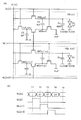
次に、図2に示す表示装置の画素10に図7(A)に示す回路ブロックを適用した構成(図9(A)参照)のシミュレーション結果を説明する。パラメータは以下の通りであり、トランジスタサイズはL/W=4μm/40μm(画素10が有するトランジスタ)、容量素子C1、C2の容量値は5pF、容量素子Csの容量値は500fF、液晶素子Clcの容量値は1pF、画像データ(DATA)は最大5V、“Vref”、“Vr”は0V、共通電極CsCOMおよびTCOMは0Vとした。また、トランジスタのゲートに印加する電圧は、“H”として+20V、“L”として−20Vとした。なお、回路シミュレーションソフトウェアにはSPICEを用いた。
Next, a simulation result of a configuration in which the circuit block illustrated in FIG. 7A is applied to the pixel 10 of the display device illustrated in FIG. 2 (see FIG. 9A) will be described. The parameters are as follows, the transistor size is L / W = 4 μm / 40 μm (transistor included in the pixel 10), the capacitance values of the capacitors C1 and C2 are 5 pF, the capacitance value of the capacitor Cs is 500 fF, and the liquid crystal device Clc The capacitance value was 1 pF, the image data (DATA) was 5 V at the maximum, “V ref ” and “V r ” were 0 V, and the common electrodes CsCOM and TCOM were 0 V. The voltage applied to the gate of the transistor was set to + 20V for “H” and −20V for “L”. Note that SPICE was used as the circuit simulation software.
図9(A)に示す回路を図9(B)に示すタイミングチャートに従って動作させた場合のシミュレーション結果を図10に示す。
FIG. 10 shows a simulation result when the circuit shown in FIG. 9A is operated according to the timing chart shown in FIG.
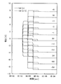
図10は、画像データ(DATA)として+5Vを入力したときのノードNM[n]、およびノードNM[n+1]における電圧のシミュレーション結果である。ノードNM[n]では、GL[n]を“H”としたタイミングで1回目の書き込みが行われ、GL[n+1]を“H”としたタイミングで2回目の書き込みが行われ、画像データ(DATA)が供給側と被供給側との容量比に従って加算されていることが確かめられた。ノードNM[n+1]も同様である。
FIG. 10 shows simulation results of voltages at the node NM [n] and the node NM [n + 1] when +5 V is input as image data (DATA). In the node NM [n], the first writing is performed at a timing when GL [n] is set to “H”, and the second writing is performed at a timing when GL [n + 1] is set to “H”. It was confirmed that (DATA) was added according to the capacity ratio between the supply side and the supply side. The same applies to the node NM [n + 1].
図11は、画像データ(DATA)として−5V乃至+5Vを入力したときのノードNM[n]、およびノードNM[n+1]における電圧のシミュレーション結果である。いずれの場合においても画像データ(DATA)が供給側と被供給側との容量比に従って加算されていることが確かめられた。
FIG. 11 shows simulation results of voltages at the node NM [n] and the node NM [n + 1] when -5V to + 5V is input as image data (DATA). In any case, it was confirmed that the image data (DATA) was added according to the capacity ratio between the supply side and the supply side.
以上のシミュレーション結果により、二つのノードに保持した電位を加算して表示素子に供給できることが確かめられた。本発明の一態様の表示装置では垂直方向の画素間における並列動作も可能であり、高速動作を必要とする表示装置に適用することが好ましい。
From the above simulation results, it was confirmed that the potentials held at the two nodes can be added and supplied to the display element. The display device of one embodiment of the present invention can operate in parallel between pixels in the vertical direction, and is preferably applied to a display device that requires high-speed operation.
本実施の形態は、他の実施の形態などに記載した構成と適宜組み合わせて実施することが可能である。
This embodiment can be implemented in appropriate combination with the structures described in the other embodiments.
(実施の形態2)
本実施の形態では、液晶素子を用いた表示装置の構成例と、EL素子を用いた表示装置の構成例について説明する。なお、本実施の形態においては、実施の形態1で説明した表示装置の要素、動作および機能の説明は省略する。
(Embodiment 2)
In this embodiment, a structure example of a display device using a liquid crystal element and a structure example of a display device using an EL element will be described. Note that in this embodiment, description of elements, operations, and functions of the display device described in Embodiment 1 is omitted.
図12(A)乃至(C)は、本発明の一態様を用いることのできる表示装置の構成を示す図である。
12A to 12C illustrate a structure of a display device in which one embodiment of the present invention can be used.
図12(A)において、第1の基板4001上に設けられた表示部215を囲むようにして、シール材4005が設けられ、表示部215がシール材4005および第2の基板4006によって封止されている。
12A, a sealant 4005 is provided so as to surround the display portion 215 provided over the first substrate 4001, and the display portion 215 is sealed with the sealant 4005 and the second substrate 4006. .
表示部215には、実施の形態1で説明した画素10等を設けることができる。なお、以下に説明する走査線駆動回路はゲートドライバ、信号線駆動回路はソースドライバに相当する。
The display portion 215 can be provided with the pixel 10 or the like described in Embodiment 1. Note that a scanning line driver circuit described below corresponds to a gate driver, and a signal line driver circuit corresponds to a source driver.
図12(A)では、走査線駆動回路221a、信号線駆動回路231a、信号線駆動回路232a、および共通線駆動回路241aは、それぞれがプリント基板4041上に設けられた集積回路4042を複数有する。集積回路4042は、単結晶半導体または多結晶半導体で形成されている。共通線駆動回路241aは、実施の形態1に示した配線128、129、132、133などに規定の電位を供給する機能を有する。
In FIG. 12A, the scan line driver circuit 221a, the signal line driver circuit 231a, the signal line driver circuit 232a, and the common line driver circuit 241a each include a plurality of integrated circuits 4042 provided over the printed board 4041. The integrated circuit 4042 is formed using a single crystal semiconductor or a polycrystalline semiconductor. The common line driver circuit 241a has a function of supplying a predetermined potential to the wirings 128, 129, 132, 133, and the like described in Embodiment 1.
走査線駆動回路221a、共通線駆動回路241a、信号線駆動回路231a、および信号線駆動回路232aに与えられる各種信号および電位は、FPC(Flexible printed circuit)4018を介して供給される。
Various signals and potentials supplied to the scan line driver circuit 221a, the common line driver circuit 241a, the signal line driver circuit 231a, and the signal line driver circuit 232a are supplied through an FPC (Flexible Printed Circuit) 4018.
走査線駆動回路221aおよび共通線駆動回路241aが有する集積回路4042は、表示部215に選択信号を供給する機能を有する。信号線駆動回路231aおよび信号線駆動回路232aが有する集積回路4042は、表示部215に画像データを供給する機能を有する。集積回路4042は、第1の基板4001上のシール材4005によって囲まれている領域とは異なる領域に実装されている。
An integrated circuit 4042 included in the scan line driver circuit 221 a and the common line driver circuit 241 a has a function of supplying a selection signal to the display portion 215. The integrated circuit 4042 included in the signal line driver circuit 231a and the signal line driver circuit 232a has a function of supplying image data to the display portion 215. The integrated circuit 4042 is mounted in a region different from the region surrounded by the sealant 4005 over the first substrate 4001.
なお、集積回路4042の接続方法は、特に限定されるものではなく、ワイヤボンディング法、COG(Chip On Glass)法、TCP(Tape Carrier Package)法、COF(Chip On Film)法などを用いることができる。
Note that a connection method of the integrated circuit 4042 is not particularly limited, and a wire bonding method, a COG (Chip On Glass) method, a TCP (Tape Carrier Package) method, a COF (Chip On Film) method, or the like can be used. it can.
図12(B)は、信号線駆動回路231aおよび信号線駆動回路232aに含まれる集積回路4042をCOG法により実装する例を示している。また、駆動回路の一部または全体を表示部215と同じ基板上に一体形成して、システムオンパネルを形成することができる。
FIG. 12B illustrates an example in which the integrated circuit 4042 included in the signal line driver circuit 231a and the signal line driver circuit 232a is mounted by a COG method. In addition, a part of or the entire driver circuit can be formed over the same substrate as the display portion 215 to form a system-on-panel.
図12(B)では、走査線駆動回路221aおよび共通線駆動回路241aを、表示部215と同じ基板上に形成する例を示している。駆動回路を表示部215内の画素回路と同時に形成することで、部品点数を削減することができる。よって、生産性を高めることができる。
FIG. 12B illustrates an example in which the scan line driver circuit 221a and the common line driver circuit 241a are formed over the same substrate as the display portion 215. By forming the driver circuit simultaneously with the pixel circuit in the display portion 215, the number of components can be reduced. Therefore, productivity can be improved.
また、図12(B)では、第1の基板4001上に設けられた表示部215と、走査線駆動回路221aおよび共通線駆動回路241aと、を囲むようにして、シール材4005が設けられている。また表示部215、走査線駆動回路221a、および共通線駆動回路241aの上に第2の基板4006が設けられている。よって、表示部215、走査線駆動回路221a、および共通線駆動回路241aは、第1の基板4001とシール材4005と第2の基板4006とによって、表示素子と共に封止されている。
In FIG. 12B, a sealant 4005 is provided so as to surround the display portion 215 provided over the first substrate 4001, the scan line driver circuit 221a, and the common line driver circuit 241a. In addition, a second substrate 4006 is provided over the display portion 215, the scan line driver circuit 221a, and the common line driver circuit 241a. Therefore, the display portion 215, the scan line driver circuit 221a, and the common line driver circuit 241a are sealed together with the display element by the first substrate 4001, the sealant 4005, and the second substrate 4006.
また、図12(B)では、信号線駆動回路231aおよび信号線駆動回路232aを別途形成し、第1の基板4001に実装している例を示しているが、この構成に限定されない。走査線駆動回路を別途形成して実装しても良いし、信号線駆動回路の一部または走査線駆動回路の一部を別途形成して実装しても良い。また、図12(C)に示すように、信号線駆動回路231aおよび信号線駆動回路232aを表示部215と同じ基板上に形成してもよい。
FIG. 12B illustrates an example in which the signal line driver circuit 231a and the signal line driver circuit 232a are separately formed and mounted on the first substrate 4001, but the present invention is not limited to this structure. The scan line driver circuit may be separately formed and then mounted, or part of the signal line driver circuit or part of the scan line driver circuit may be separately formed and then mounted. In addition, as illustrated in FIG. 12C, the signal line driver circuit 231a and the signal line driver circuit 232a may be formed over the same substrate as the display portion 215.
また、表示装置は、表示素子が封止された状態にあるパネルと、該パネルにコントローラを含むIC等を実装した状態にあるモジュールとを含む場合がある。
In some cases, the display device includes a panel in which the display element is sealed, and a module in which an IC including a controller or the like is mounted on the panel.
また第1の基板上に設けられた表示部および走査線駆動回路は、トランジスタを複数有している。当該トランジスタとして、上記実施の形態で示したトランジスタを適用することができる。
The display portion and the scan line driver circuit provided over the first substrate include a plurality of transistors. The transistor described in any of the above embodiments can be used as the transistor.
周辺駆動回路が有するトランジスタと、表示部の画素回路が有するトランジスタの構造は同じであってもよく、異なっていてもよい。周辺駆動回路が有するトランジスタは、全て同じ構造のトランジスタであってもよく、2種類以上の構造のトランジスタを有していてもよい。同様に、画素回路が有するトランジスタは、全て同じ構造のトランジスタであってもよく、2種類以上の構造のトランジスタを有していてもよい。
The transistor included in the peripheral driver circuit and the transistor included in the pixel circuit in the display portion may have the same structure or different structures. The transistors included in the peripheral driver circuit may all have the same structure, or may have two or more types of transistors. Similarly, the transistors included in the pixel circuit may all have the same structure or may have two or more types of transistors.
また、第2の基板4006上には入力装置4200を設けることができる。図12(A)乃至(C)に示す表示装置に入力装置4200を設けた構成はタッチパネルとして機能させることができる。
In addition, the input device 4200 can be provided over the second substrate 4006. The structure in which the input device 4200 is provided in the display device illustrated in FIGS. 12A to 12C can function as a touch panel.
本発明の一態様のタッチパネルが有する検知素子(センサ素子ともいう)に限定は無い。指やスタイラスなどの被検知体の近接または接触を検知することのできる様々なセンサを、検知素子として適用することができる。
There is no limitation on a detection element (also referred to as a sensor element) included in the touch panel of one embodiment of the present invention. Various sensors that can detect the proximity or contact of an object to be detected, such as a finger or a stylus, can be applied as the detection element.
センサの方式としては、例えば、静電容量方式、抵抗膜方式、表面弾性波方式、赤外線方式、光学方式、感圧方式など様々な方式を用いることができる。
As a sensor method, for example, various methods such as a capacitance method, a resistance film method, a surface acoustic wave method, an infrared method, an optical method, and a pressure-sensitive method can be used.
本実施の形態では、静電容量方式の検知素子を有するタッチパネルを例に挙げて説明する。
In this embodiment, a touch panel having a capacitive detection element will be described as an example.
静電容量方式としては、表面型静電容量方式、投影型静電容量方式等がある。また、投影型静電容量方式としては、自己容量方式、相互容量方式等がある。相互容量方式を用いると、同時多点検知が可能となるため好ましい。
Examples of the electrostatic capacity method include a surface electrostatic capacity method and a projection electrostatic capacity method. In addition, examples of the projected capacitance method include a self-capacitance method and a mutual capacitance method. The mutual capacitance method is preferable because simultaneous multipoint detection is possible.
本発明の一態様のタッチパネルは、別々に作製された表示装置と検知素子とを貼り合わせる構成、表示素子を支持する基板および対向基板の一方または双方に検知素子を構成する電極等を設ける構成等、様々な構成を適用することができる。
The touch panel of one embodiment of the present invention includes a structure in which a separately manufactured display device and a detection element are attached, a structure in which an electrode that forms the detection element is provided on one or both of a substrate that supports the display element and a counter substrate, and the like Various configurations can be applied.
図13(A)、(B)に、タッチパネルの一例を示す。図13(A)は、タッチパネル4210の斜視図である。図13(B)は、入力装置4200の斜視概略図である。なお、明瞭化のため、代表的な構成要素のみを示している。
FIGS. 13A and 13B show an example of a touch panel. FIG. 13A is a perspective view of the touch panel 4210. FIG. 13B is a schematic perspective view of the input device 4200. For the sake of clarity, only representative components are shown.
タッチパネル4210は、別々に作製された表示装置と検知素子とを貼り合わせた構成である。
The touch panel 4210 has a structure in which a separately manufactured display device and a detection element are bonded to each other.
タッチパネル4210は、入力装置4200と、表示装置とを有し、これらが重ねて設けられている。
The touch panel 4210 includes an input device 4200 and a display device, which are provided to overlap each other.
入力装置4200は、基板4263、電極4227、電極4228、複数の配線4237、複数の配線4238および複数の配線4239を有する。例えば、電極4227は配線4237または配線4239と電気的に接続することができる。また、電極4228は配線4239と電気的に接続することができる。FPC4272bは、複数の配線4237および複数の配線4238の各々と電気的に接続する。FPC4272bにはIC4273bを設けることができる。
The input device 4200 includes a substrate 4263, an electrode 4227, an electrode 4228, a plurality of wirings 4237, a plurality of wirings 4238, and a plurality of wirings 4239. For example, the electrode 4227 can be electrically connected to the wiring 4237 or the wiring 4239. The electrode 4228 can be electrically connected to the wiring 4239. The FPC 4272b is electrically connected to each of the plurality of wirings 4237 and the plurality of wirings 4238. The FPC 4272b can be provided with an IC 4273b.
または、表示装置の第1の基板4001と第2の基板4006との間にタッチセンサを設けてもよい。第1の基板4001と第2の基板4006との間にタッチセンサを設ける場合は、静電容量方式のタッチセンサのほか、光電変換素子を用いた光学式のタッチセンサを適用してもよい。
Alternatively, a touch sensor may be provided between the first substrate 4001 and the second substrate 4006 of the display device. In the case where a touch sensor is provided between the first substrate 4001 and the second substrate 4006, an optical touch sensor using a photoelectric conversion element may be used in addition to a capacitive touch sensor.
図14(A)、(B)は、図12(B)中でN1−N2の鎖線で示した部位の断面図である。図14(A)、(B)に示す表示装置は電極4015を有しており、電極4015はFPC4018が有する端子と異方性導電層4019を介して、電気的に接続されている。また、図14(A)、(B)では、電極4015は、絶縁層4112、絶縁層4111、および絶縁層4110に形成された開口において配線4014と電気的に接続されている。
14A and 14B are cross-sectional views of a portion indicated by a chain line N1-N2 in FIG. 12B. 14A and 14B includes an electrode 4015, and the electrode 4015 is electrically connected to a terminal included in the FPC 4018 through an anisotropic conductive layer 4019. The display device illustrated in FIGS. In FIGS. 14A and 14B, the electrode 4015 is electrically connected to the wiring 4014 in the opening formed in the insulating layer 4112, the insulating layer 4111, and the insulating layer 4110.
電極4015は、第1の電極層4030と同じ導電層から形成され、配線4014は、トランジスタ4010、およびトランジスタ4011のソース電極およびドレイン電極と同じ導電層で形成されている。
The electrode 4015 is formed using the same conductive layer as the first electrode layer 4030, and the wiring 4014 is formed using the same conductive layer as the source electrode and the drain electrode of the transistor 4010 and the transistor 4011.
また、第1の基板4001上に設けられた表示部215と走査線駆動回路221aは、トランジスタを複数有しており、図14(A)、(B)では、表示部215に含まれるトランジスタ4010、および走査線駆動回路221aに含まれるトランジスタ4011を例示している。なお、図14(A)、(B)では、トランジスタ4010およびトランジスタ4011としてボトムゲート型のトランジスタを例示しているが、トップゲート型のトランジスタであってもよい。
In addition, the display portion 215 and the scan line driver circuit 221a provided over the first substrate 4001 include a plurality of transistors. In FIGS. 14A and 14B, the transistor 4010 included in the display portion 215 is included. , And a transistor 4011 included in the scan line driver circuit 221a. 14A and 14B illustrate bottom-gate transistors as the transistor 4010 and the transistor 4011, a top-gate transistor may be used.
図14(A)、(B)では、トランジスタ4010およびトランジスタ4011上に絶縁層4112が設けられている。また、図14(B)では、絶縁層4112上に隔壁4510が形成されている。
14A and 14B, the insulating layer 4112 is provided over the transistors 4010 and 4011. In FIG. 14B, a partition wall 4510 is formed over the insulating layer 4112.
また、トランジスタ4010およびトランジスタ4011は、絶縁層4102上に設けられている。また、トランジスタ4010およびトランジスタ4011は、絶縁層4111上に形成された電極4017を有する。電極4017はバックゲート電極として機能することができる。
In addition, the transistor 4010 and the transistor 4011 are provided over the insulating layer 4102. In addition, the transistor 4010 and the transistor 4011 include an electrode 4017 formed over the insulating layer 4111. The electrode 4017 can function as a back gate electrode.
また、図14(A)、(B)に示す表示装置は、容量素子4020を有する。容量素子4020は、トランジスタ4010のゲート電極と同じ工程で形成された電極4021と、ソース電極およびドレイン電極と同じ工程で形成された電極と、を有する。それぞれの電極は、絶縁層4103を介して重なっている。
In addition, the display device illustrated in FIGS. 14A and 14B includes a capacitor 4020. The capacitor 4020 includes an electrode 4021 formed in the same step as the gate electrode of the transistor 4010 and an electrode formed in the same step as the source electrode and the drain electrode. Each electrode overlaps with the insulating layer 4103 interposed therebetween.
一般に、表示装置の画素部に設けられる容量素子の容量は、画素部に配置されるトランジスタのリーク電流等を考慮して、所定の期間の間電荷を保持できるように設定される。容量素子の容量は、トランジスタのオフ電流等を考慮して設定すればよい。
In general, the capacitance of a capacitor provided in the pixel portion of the display device is set so that charge can be held for a predetermined period in consideration of leakage current of a transistor arranged in the pixel portion. The capacity of the capacitor may be set in consideration of the off-state current of the transistor.
表示部215に設けられたトランジスタ4010は表示素子と電気的に接続する。図14(A)は、表示素子として液晶素子を用いた液晶表示装置の一例である。図14(A)において、表示素子である液晶素子4013は、第1の電極層4030、第2の電極層4031、および液晶層4008を含む。なお、液晶層4008を挟持するように配向膜として機能する絶縁層4032、絶縁層4033が設けられている。第2の電極層4031は第2の基板4006側に設けられ、第1の電極層4030と第2の電極層4031は液晶層4008を介して重畳する。
The transistor 4010 provided in the display portion 215 is electrically connected to the display element. FIG. 14A illustrates an example of a liquid crystal display device using a liquid crystal element as a display element. In FIG. 14A, a liquid crystal element 4013 which is a display element includes a first electrode layer 4030, a second electrode layer 4031, and a liquid crystal layer 4008. Note that an insulating layer 4032 and an insulating layer 4033 which function as alignment films are provided so as to sandwich the liquid crystal layer 4008. The second electrode layer 4031 is provided on the second substrate 4006 side, and the first electrode layer 4030 and the second electrode layer 4031 overlap with each other with the liquid crystal layer 4008 interposed therebetween.
また、スペーサ4035は絶縁層を選択的にエッチングすることで得られる柱状のスペーサであり、第1の電極層4030と第2の電極層4031との間隔(セルギャップ)を制御するために設けられている。なお球状のスペーサを用いていても良い。
The spacer 4035 is a columnar spacer obtained by selectively etching the insulating layer, and is provided to control the distance (cell gap) between the first electrode layer 4030 and the second electrode layer 4031. ing. A spherical spacer may be used.
また、必要に応じて、ブラックマトリクス(遮光層)、着色層(カラーフィルタ)、偏光部材、位相差部材、反射防止部材などの光学部材(光学基板)などを適宜設けてもよい。例えば、偏光基板および位相差基板による円偏光を用いてもよい。また、光源としてバックライト、サイドライトなどを用いてもよい。また、上記バックライト、およびサイドライトとして、マイクロLEDなどを用いても良い。
If necessary, an optical member (optical substrate) such as a black matrix (light-shielding layer), a colored layer (color filter), a polarizing member, a retardation member, or an antireflection member may be provided as appropriate. For example, circularly polarized light using a polarizing substrate and a retardation substrate may be used. Further, a backlight, a sidelight, or the like may be used as the light source. Further, a micro LED or the like may be used as the backlight and the sidelight.
図14(A)に示す表示装置では、第2の基板4006と第2の電極層4031の間に、遮光層4132、着色層4131、絶縁層4133が設けられている。
In the display device illustrated in FIG. 14A, a light-blocking layer 4132, a colored layer 4131, and an insulating layer 4133 are provided between the second substrate 4006 and the second electrode layer 4031.
遮光層として用いることのできる材料としては、カーボンブラック、チタンブラック、金属、金属酸化物、複数の金属酸化物の固溶体を含む複合酸化物等が挙げられる。遮光層は、樹脂材料を含む膜であってもよいし、金属などの無機材料の薄膜であってもよい。また、遮光層に、着色層の材料を含む膜の積層膜を用いることもできる。例えば、ある色の光を透過する着色層に用いる材料を含む膜と、他の色の光を透過する着色層に用いる材料を含む膜との積層構造を用いることができる。着色層と遮光層の材料を共通化することで、装置を共通化できるほか工程を簡略化できるため好ましい。
Examples of the material that can be used for the light-shielding layer include carbon black, titanium black, metal, metal oxide, and composite oxide containing a solid solution of a plurality of metal oxides. The light shielding layer may be a film containing a resin material or a thin film of an inorganic material such as a metal. Alternatively, a stacked film of a film containing a material for the colored layer can be used for the light shielding layer. For example, a stacked structure of a film including a material used for a colored layer that transmits light of a certain color and a film including a material used for a colored layer that transmits light of another color can be used. It is preferable to use a common material for the coloring layer and the light-shielding layer because the apparatus can be shared and the process can be simplified.
着色層に用いることのできる材料としては、金属材料、樹脂材料、顔料または染料が含まれた樹脂材料などが挙げられる。遮光層および着色層は、例えば、インクジェット法などを用いて形成することができる。
Examples of materials that can be used for the colored layer include metal materials, resin materials, resin materials containing pigments or dyes, and the like. The light shielding layer and the colored layer can be formed using, for example, an inkjet method.
また、図14(A)、(B)に示す表示装置は、絶縁層4111と絶縁層4104を有する。絶縁層4111と絶縁層4104として、不純物元素を透過しにくい絶縁層を用いる。絶縁層4111と絶縁層4104でトランジスタの半導体層を挟むことで、外部からの不純物の浸入を防ぐことができる。
In addition, the display device illustrated in FIGS. 14A and 14B includes an insulating layer 4111 and an insulating layer 4104. As the insulating layer 4111 and the insulating layer 4104, insulating layers that hardly transmit an impurity element are used. By sandwiching the semiconductor layer of the transistor between the insulating layer 4111 and the insulating layer 4104, entry of impurities from the outside can be prevented.
また、表示装置に含まれる表示素子として、エレクトロルミネッセンスを利用する発光素子(EL素子)を適用することができる。EL素子は、一対の電極の間に発光性の化合物を含む層(「EL層」ともいう。)を有する。一対の電極間に、EL素子の閾値電圧よりも大きい電位差を生じさせると、EL層に陽極側から正孔が注入され、陰極側から電子が注入される。注入された電子と正孔はEL層において再結合し、EL層に含まれる発光性の化合物が発光する。
In addition, as a display element included in the display device, a light-emitting element (EL element) using electroluminescence can be used. An EL element includes a layer containing a light-emitting compound (also referred to as an “EL layer”) between a pair of electrodes. When a potential difference larger than the threshold voltage of the EL element is generated between the pair of electrodes, holes are injected into the EL layer from the anode side and electrons are injected from the cathode side. The injected electrons and holes are recombined in the EL layer, and a light-emitting compound contained in the EL layer emits light.
また、EL素子は、発光材料が有機化合物であるか、無機化合物であるかによって区別され、一般的に、前者は有機EL素子、後者は無機EL素子と呼ばれている。なお、発光材料として化合物半導体を用いるLED(マイクロLEDを含む)もEL素子の一つである。
The EL element is distinguished depending on whether the light emitting material is an organic compound or an inorganic compound, and the former is generally called an organic EL element and the latter is called an inorganic EL element. Note that an LED (including a micro LED) using a compound semiconductor as a light-emitting material is also one of EL elements.
有機EL素子は、電圧を印加することにより、一方の電極から電子、他方の電極から正孔がそれぞれEL層に注入される。そして、それらキャリア(電子および正孔)が再結合することにより、発光性の有機化合物が励起状態を形成し、その励起状態が基底状態に戻る際に発光する。このようなメカニズムから、このような発光素子は、電流励起型の発光素子と呼ばれる。
In the organic EL element, by applying a voltage, electrons from one electrode and holes from the other electrode are injected into the EL layer. Then, these carriers (electrons and holes) recombine, whereby the light-emitting organic compound forms an excited state, and emits light when the excited state returns to the ground state. Due to such a mechanism, such a light-emitting element is referred to as a current-excitation light-emitting element.
なお、EL層は、発光性の化合物以外に、正孔注入性の高い物質、正孔輸送性の高い物質、正孔ブロック材料、電子輸送性の高い物質、電子注入性の高い物質、またはバイポーラ性の物質(電子輸送性および正孔輸送性が高い物質)などを有していてもよい。
Note that in addition to the light-emitting compound, the EL layer includes a substance having a high hole-injecting property, a substance having a high hole-transporting property, a hole blocking material, a substance having a high electron-transporting property, a substance having a high electron-injecting property, or a bipolar layer. Material (a material having a high electron transporting property and a high hole transporting property) may be included.
EL層は、蒸着法(真空蒸着法を含む)、転写法、印刷法、インクジェット法、塗布法などの方法で形成することができる。
The EL layer can be formed by a method such as a vapor deposition method (including a vacuum vapor deposition method), a transfer method, a printing method, an ink jet method, or a coating method.
無機EL素子は、その素子構成により、分散型無機EL素子と薄膜型無機EL素子とに分類される。分散型無機EL素子は、発光材料の粒子をバインダ中に分散させた発光層を有するものであり、発光メカニズムはドナー準位とアクセプター準位を利用するドナー−アクセプター再結合型発光である。薄膜型無機EL素子は、発光層を誘電体層で挟み込み、さらにそれを電極で挟んだ構造であり、発光メカニズムは金属イオンの内殻電子遷移を利用する局在型発光である。なお、ここでは、発光素子として有機EL素子を用いて説明する。
Inorganic EL elements are classified into a dispersion-type inorganic EL element and a thin-film inorganic EL element depending on the element structure. The dispersion-type inorganic EL element has a light-emitting layer in which particles of a light-emitting material are dispersed in a binder, and the light emission mechanism is donor-acceptor recombination light emission using a donor level and an acceptor level. The thin-film inorganic EL element has a structure in which a light emitting layer is sandwiched between dielectric layers and further sandwiched between electrodes, and the light emission mechanism is localized light emission utilizing inner-shell electron transition of metal ions. Note that description is made here using an organic EL element as a light-emitting element.
発光素子は発光を取り出すために少なくとも一対の電極の一方が透明であればよい。そして、基板上にトランジスタおよび発光素子を形成し、当該基板とは逆側の面から発光を取り出す上面射出(トップエミッション)構造や、基板側の面から発光を取り出す下面射出(ボトムエミッション)構造や、両面から発光を取り出す両面射出(デュアルエミッション)構造の発光素子があり、どの射出構造の発光素子も適用することができる。
In order to extract light emitted from the light-emitting element, at least one of the pair of electrodes may be transparent. Then, a transistor and a light emitting element are formed over the substrate, and a top emission structure that extracts light from a surface opposite to the substrate, a bottom emission structure that extracts light from a surface on the substrate side, There is a light emitting element having a dual emission structure in which light emission is extracted from both sides, and any light emitting element having an emission structure can be applied.
図14(B)は、表示素子として発光素子を用いた発光表示装置(「EL表示装置」ともいう。)の一例である。表示素子である発光素子4513は、表示部215に設けられたトランジスタ4010と電気的に接続している。なお発光素子4513の構成は、第1の電極層4030、発光層4511、第2の電極層4031の積層構造であるが、この構成に限定されない。発光素子4513から取り出す光の方向などに合わせて、発光素子4513の構成は適宜変えることができる。
FIG. 14B illustrates an example of a light-emitting display device (also referred to as an “EL display device”) using a light-emitting element as a display element. A light-emitting element 4513 which is a display element is electrically connected to a transistor 4010 provided in the display portion 215. Note that the structure of the light-emitting element 4513 is a stacked structure of the first electrode layer 4030, the light-emitting layer 4511, and the second electrode layer 4031; however, the structure is not limited to this structure. The structure of the light-emitting element 4513 can be changed as appropriate depending on the direction in which light is extracted from the light-emitting element 4513, or the like.
隔壁4510は、有機絶縁材料、または無機絶縁材料を用いて形成する。特に感光性の樹脂材料を用い、第1の電極層4030上に開口部を形成し、その開口部の側面が連続した曲率を持って形成される傾斜面となるように形成することが好ましい。
A partition wall 4510 is formed using an organic insulating material or an inorganic insulating material. In particular, it is preferable to use a photosensitive resin material and form an opening on the first electrode layer 4030 so that the side surface of the opening is an inclined surface formed with a continuous curvature.
発光層4511は、単数の層で構成されていても、複数の層が積層されるように構成されていてもどちらでも良い。
The light emitting layer 4511 may be composed of a single layer or a plurality of layers stacked.
発光素子4513の発光色は、発光層4511を構成する材料によって、白、赤、緑、青、シアン、マゼンタ、または黄などとすることができる。
The light emission color of the light emitting element 4513 can be white, red, green, blue, cyan, magenta, yellow, or the like depending on the material forming the light emitting layer 4511.
カラー表示を実現する方法としては、発光色が白色の発光素子4513と着色層を組み合わせて行う方法と、画素毎に発光色の異なる発光素子4513を設ける方法がある。前者の方法は後者の方法よりも生産性が高い。一方、後者の方法では画素毎に発光層4511を作り分ける必要があるため、前者の方法よりも生産性が劣る。ただし、後者の方法では、前者の方法よりも色純度の高い発光色を得ることができる。後者の方法に加えて、発光素子4513にマイクロキャビティ構造を付与することにより色純度をさらに高めることができる。
As a method for realizing color display, there are a method in which a light emitting element 4513 having a white emission color and a colored layer are combined, and a method in which a light emitting element 4513 having a different emission color is provided for each pixel. The former method is more productive than the latter method. On the other hand, in the latter method, since it is necessary to make a light emitting layer 4511 for each pixel, productivity is inferior to the former method. However, in the latter method, it is possible to obtain an emission color with higher color purity than in the former method. In addition to the latter method, the color purity can be further increased by providing the light-emitting element 4513 with a microcavity structure.
なお、発光層4511は、量子ドットなどの無機化合物を有していてもよい。例えば、量子ドットを発光層に用いることで、発光材料として機能させることもできる。
Note that the light-emitting layer 4511 may include an inorganic compound such as a quantum dot. For example, a quantum dot can be used for a light emitting layer to function as a light emitting material.
発光素子4513に酸素、水素、水分、二酸化炭素等が侵入しないように、第2の電極層4031および隔壁4510上に保護層を形成してもよい。保護層としては、窒化シリコン、窒化酸化シリコン、酸化アルミニウム、窒化アルミニウム、酸化窒化アルミニウム、窒化酸化アルミニウム、DLC(Diamond Like Carbon)などを形成することができる。また、第1の基板4001、第2の基板4006、およびシール材4005によって封止された空間には充填材4514が設けられ密封されている。このように、外気に曝されないように気密性が高く、脱ガスの少ない保護フィルム(貼り合わせフィルム、紫外線硬化樹脂フィルム等)やカバー材でパッケージング(封入)することが好ましい。
A protective layer may be formed over the second electrode layer 4031 and the partition wall 4510 so that oxygen, hydrogen, moisture, carbon dioxide, or the like does not enter the light-emitting element 4513. As the protective layer, silicon nitride, silicon nitride oxide, aluminum oxide, aluminum nitride, aluminum oxynitride, aluminum nitride oxide, DLC (Diamond Like Carbon), or the like can be formed. In addition, a filler 4514 is provided and sealed in a space sealed by the first substrate 4001, the second substrate 4006, and the sealant 4005. As described above, it is preferable to package (enclose) the protective film with a protective film (bonded film, ultraviolet curable resin film, or the like) or a cover material that has high hermeticity and little degassing so as not to be exposed to the outside air.
充填材4514としては窒素やアルゴンなどの不活性な気体の他に、紫外線硬化樹脂または熱硬化樹脂を用いることができ、PVC(ポリビニルクロライド)、アクリル系樹脂、ポリイミド、エポキシ系樹脂、シリコーン系樹脂、PVB(ポリビニルブチラル)またはEVA(エチレンビニルアセテート)などを用いることができる。また、充填材4514に乾燥剤が含まれていてもよい。
In addition to an inert gas such as nitrogen or argon, an ultraviolet curable resin or a thermosetting resin can be used as the filler 4514. PVC (polyvinyl chloride), acrylic resin, polyimide, epoxy resin, silicone resin PVB (polyvinyl butyral) or EVA (ethylene vinyl acetate) can be used. Further, the filler 4514 may contain a desiccant.
シール材4005には、ガラスフリットなどのガラス材料や、二液混合型の樹脂などの常温で硬化する硬化樹脂、光硬化性の樹脂、熱硬化性の樹脂などの樹脂材料を用いることができる。また、シール材4005に乾燥剤が含まれていてもよい。
As the sealant 4005, a glass material such as glass frit, or a resin material such as a two-component mixed resin, a curable resin that cures at normal temperature, a photocurable resin, or a thermosetting resin can be used. Further, the sealing material 4005 may contain a desiccant.
また、必要であれば、発光素子の射出面に偏光板、または円偏光板(楕円偏光板を含む)、位相差板(λ/4板、λ/2板)、カラーフィルタなどの光学フィルムを適宜設けてもよい。また、偏光板または円偏光板に反射防止膜を設けてもよい。例えば、表面の凹凸により反射光を拡散し、映り込みを低減できるアンチグレア処理を施すことができる。
Further, if necessary, an optical film such as a polarizing plate, a circularly polarizing plate (including an elliptical polarizing plate), a retardation plate (λ / 4 plate, λ / 2 plate), a color filter, or the like is provided on the emission surface of the light emitting element. You may provide suitably. Further, an antireflection film may be provided on the polarizing plate or the circularly polarizing plate. For example, anti-glare treatment can be performed that diffuses reflected light due to surface irregularities and reduces reflection.
また、発光素子をマイクロキャビティ構造とすることで、色純度の高い光を取り出すことができる。また、マイクロキャビティ構造とカラーフィルタを組み合わせることで、映り込みが低減し、表示画像の視認性を高めることができる。
In addition, when the light-emitting element has a microcavity structure, light with high color purity can be extracted. Further, by combining the microcavity structure and the color filter, the reflection can be reduced and the visibility of the display image can be improved.
表示素子に電圧を印加する第1の電極層および第2の電極層(画素電極層、共通電極層、対向電極層などともいう)においては、取り出す光の方向、電極層が設けられる場所、および電極層のパターン構造によって透光性、反射性を選択すればよい。
In the first electrode layer and the second electrode layer (also referred to as a pixel electrode layer, a common electrode layer, a counter electrode layer, and the like) that apply a voltage to the display element, a direction of light to be extracted, a place where the electrode layer is provided, and What is necessary is just to select translucency and reflectivity by the pattern structure of an electrode layer.
第1の電極層4030、第2の電極層4031は、酸化タングステンを含むインジウム酸化物、酸化タングステンを含むインジウム亜鉛酸化物、酸化チタンを含むインジウム酸化物、インジウム錫酸化物、酸化チタンを含むインジウム錫酸化物、インジウム亜鉛酸化物、酸化ケイ素を添加したインジウム錫酸化物などの透光性を有する導電性材料を用いることができる。
The first electrode layer 4030 and the second electrode layer 4031 include indium oxide containing tungsten oxide, indium zinc oxide containing tungsten oxide, indium oxide containing titanium oxide, indium tin oxide, and indium containing titanium oxide. A light-transmitting conductive material such as tin oxide, indium zinc oxide, or indium tin oxide to which silicon oxide is added can be used.
また、第1の電極層4030、第2の電極層4031はタングステン(W)、モリブデン(Mo)、ジルコニウム(Zr)、ハフニウム(Hf)、バナジウム(V)、ニオブ(Nb)、タンタル(Ta)、クロム(Cr)、コバルト(Co)、ニッケル(Ni)、チタン(Ti)、白金(Pt)、アルミニウム(Al)、銅(Cu)、銀(Ag)などの金属、またはその合金、もしくはその金属窒化物から一種以上を用いて形成することができる。
The first electrode layer 4030 and the second electrode layer 4031 are tungsten (W), molybdenum (Mo), zirconium (Zr), hafnium (Hf), vanadium (V), niobium (Nb), and tantalum (Ta). , Chromium (Cr), cobalt (Co), nickel (Ni), titanium (Ti), platinum (Pt), aluminum (Al), copper (Cu), silver (Ag) and other metals, or alloys thereof, or One or more metal nitrides can be used.
また、第1の電極層4030、第2の電極層4031として、導電性高分子(導電性ポリマーともいう)を含む導電性組成物を用いて形成することができる。導電性高分子としては、いわゆるπ電子共役系導電性高分子を用いることができる。例えば、ポリアニリン若しくはその誘導体、ポリピロール若しくはその誘導体、ポリチオフェン若しくはその誘導体、または、アニリン、ピロールおよびチオフェンの2種以上からなる共重合体若しくはその誘導体などがあげられる。
Alternatively, the first electrode layer 4030 and the second electrode layer 4031 can be formed using a conductive composition including a conductive high molecule (also referred to as a conductive polymer). As the conductive polymer, a so-called π-electron conjugated conductive polymer can be used. For example, polyaniline or a derivative thereof, polypyrrole or a derivative thereof, polythiophene or a derivative thereof, a copolymer of two or more of aniline, pyrrole, and thiophene or a derivative thereof can be given.
また、トランジスタは静電気などにより破壊されやすいため、駆動回路保護用の保護回路を設けることが好ましい。保護回路は、非線形素子を用いて構成することが好ましい。
In addition, since the transistor is easily broken by static electricity or the like, it is preferable to provide a protective circuit for protecting the driving circuit. The protection circuit is preferably configured using a non-linear element.
なお、図15に示すように、トランジスタや容量素子が高さ方向に重なる領域を有するようなスタック構造としてもよい。例えば、駆動回路を構成するトランジスタ4011およびトランジスタ4022を重ねて配置すれば、狭額縁の表示装置とすることができる。また、画素回路を構成するトランジスタ4010、トランジスタ4023、容量素子4020などが一部でも重なる領域を有するように配置すれば開口率や解像度を向上させることができる。なお、図15では図14(A)に示す液晶表示装置にスタック構造を応用した例を示しているが、図14(B)に示すEL表示装置に応用してもよい。
Note that as illustrated in FIG. 15, a stack structure in which a transistor and a capacitor are overlapped in the height direction may be employed. For example, when the transistor 4011 and the transistor 4022 included in the driver circuit are stacked, a display device with a narrow frame can be obtained. In addition, when the transistor 4010, the transistor 4023, the capacitor 4020, and the like included in the pixel circuit are arranged so as to overlap with each other, the aperture ratio and the resolution can be improved. Note that FIG. 15 illustrates an example in which the stack structure is applied to the liquid crystal display device illustrated in FIG. 14A; however, the liquid crystal display device may be applied to an EL display device illustrated in FIG.
また、画素回路において、電極や配線に可視光に対して透光性の高い透光性導電膜を用いることで、画素内の光の透過率を高めることができ、実質的に開口率を向上させることができる。なお、OSトランジスタを用いる場合は半導体層も透光性を有するため、さらに開口率を高めることができる。これらは、トランジスタ等をスタック構造としない場合においても有効である。
In addition, in the pixel circuit, by using a light-transmitting conductive film that has a high light-transmitting property with respect to visible light for electrodes and wiring, the light transmittance in the pixel can be increased, and the aperture ratio is substantially improved. Can be made. Note that when an OS transistor is used, the semiconductor layer also has a light-transmitting property, so that the aperture ratio can be further increased. These are effective even when the transistor or the like does not have a stack structure.
また、液晶表示装置と発光装置を組み合わせて表示装置を構成としてもよい。
In addition, a display device may be configured by combining a liquid crystal display device and a light-emitting device.
発光装置は表示面の逆側、または表示面の端部に配置される。発光装置は表示素子に光を供給する機能を有する。発光装置は、バックライトとも呼ぶことができる。
The light emitting device is disposed on the opposite side of the display surface or on the end of the display surface. The light-emitting device has a function of supplying light to the display element. The light emitting device can also be called a backlight.
ここで、発光装置は、板状またはシート状の導光部(導光板ともいう)と、異なる色の光を呈する複数の発光素子を有することができる。当該発光素子を導光部の側面近傍に配置すると、導光部側面から内部へ光を発することができる。導光部は光路を変更する機構(光取り出し機構ともいう)を有しており、これにより、発光装置は表示パネルの画素部に光を均一に照射することができる。または、導光部を設けず、画素の直下に発光装置を配置する構成としてもよい。
Here, the light-emitting device can include a plate-shaped or sheet-shaped light guide (also referred to as a light guide plate) and a plurality of light-emitting elements that exhibit light of different colors. When the light emitting element is disposed in the vicinity of the side surface of the light guide unit, light can be emitted from the side surface of the light guide unit to the inside. The light guide unit has a mechanism for changing an optical path (also referred to as a light extraction mechanism), whereby the light emitting device can uniformly irradiate light to the pixel portion of the display panel. Or it is good also as a structure which arrange | positions a light-emitting device directly under a pixel, without providing a light guide part.
発光装置は、赤色(R)、緑色(G)、青色(B)の3色の発光素子を有することが好ましい。さらに白色(W)の発光素子を有していてもよい。これら発光素子として発光ダイオード(LED:Light Emitting Diode)を用いることが好ましい。
The light-emitting device preferably has three color light-emitting elements of red (R), green (G), and blue (B). Further, a white (W) light emitting element may be included. It is preferable to use a light emitting diode (LED: Light Emitting Diode) as these light emitting elements.
さらに、発光素子は、その発光スペクトルの半値全幅(FWHM:Full Width at Half Maximum)が、50nm以下、好ましくは40nm以下、より好ましくは30nm以下、さらに好ましくは20nm以下である、極めて色純度の高い発光素子であることが好ましい。なお、発光スペクトルの半値全幅は、小さければ小さいほどよいが、例えば1nm以上とすることができる。これにより、カラー表示を行う際に、色再現性が高い鮮やかな表示を行うことができる。
Further, the light emitting element has a full width at half maximum (FWHM: Full Width at Half Maximum) of 50 nm or less, preferably 40 nm or less, more preferably 30 nm or less, more preferably 20 nm or less, and extremely high color purity. A light emitting element is preferable. The full width at half maximum of the emission spectrum is preferably as small as possible, but can be set to, for example, 1 nm or more. Thereby, when performing color display, vivid display with high color reproducibility can be performed.
また、赤色の発光素子は、発光スペクトルのピーク波長が、625nm以上650nm以下の範囲内に位置する素子を用いることが好ましい。また、緑色の発光素子は、発光スペクトルのピーク波長が、515nm以上540nm以下の範囲内に位置する素子を用いることが好ましい。青色の発光素子は、発光スペクトルのピーク波長が、445nm以上470nm以下の範囲内に位置する素子を用いることが好ましい。
As the red light-emitting element, an element having an emission spectrum peak wavelength in the range of 625 nm to 650 nm is preferably used. As the green light-emitting element, an element having an emission spectrum peak wavelength in the range of 515 nm to 540 nm is preferably used. As the blue light-emitting element, an element having an emission spectrum peak wavelength in the range of 445 nm to 470 nm is preferably used.
表示装置は、3色の発光素子を順次点滅させるとともに、これと同期させて画素を駆動し、継時加法混色法に基づいてカラー表示を行うことができる。当該駆動方法は、フィールドシーケンシャル駆動とも呼ぶことができる。
The display device can perform color display based on the successive additive color mixing method by sequentially flashing the light emitting elements of the three colors and driving the pixels in synchronization therewith. This driving method can also be called field sequential driving.
フィールドシーケンシャル駆動では、鮮やかなカラー画像を表示することができる。また、滑らかな動画像を表示することができる。また上記駆動方法を用いることで、1つの画素を複数の異なる色の副画素で構成する必要がなく、1つの画素の有効反射面積(有効表示面積、開口率ともいう)を大きくできるため、明るい表示を行うことができる。さらに、画素にカラーフィルタを設ける必要がないため、画素の透過率も向上させることもでき、さらに明るい表示を行うことができる。また、作製工程を簡略化でき、作製コストを低減することができる。
In field sequential driving, a vivid color image can be displayed. In addition, a smooth moving image can be displayed. In addition, by using the above driving method, it is not necessary to configure one pixel by a plurality of sub-pixels of different colors, and the effective reflection area (also referred to as an effective display area or aperture ratio) of one pixel can be increased. Display can be made. Further, since it is not necessary to provide a color filter in the pixel, the transmittance of the pixel can be improved, and a brighter display can be performed. Further, the manufacturing process can be simplified and the manufacturing cost can be reduced.
図16(A)、(B)は、フィールドシーケンシャル駆動が可能な表示装置の断面概略図の一例である。当該表示装置の基板4001側にはRGB各色の発光が可能なバックライトユニットが設けられる。なお、フィールドシーケンシャル駆動では、RGB各色の時分割発光で色を表現するため、カラーフィルタは不要となる。
16A and 16B are examples of a schematic cross-sectional view of a display device capable of field sequential driving. A backlight unit capable of emitting light of RGB colors is provided on the substrate 4001 side of the display device. In the field sequential drive, colors are expressed by time-division light emission of each color of RGB, so that a color filter is not necessary.
図16(A)に示すバックライトユニット4340aは、画素の直下に拡散板4352を介して発光素子4342が複数設けられた構成である。拡散板4352は、発光素子4342から基板4001側に射出された光を拡散し、表示部面内の輝度を均一化する機能を有する。発光素子4342と拡散板4352との間には、必要に応じて偏光板を設けてもよい。また、拡散板4352は不要であれば設けなくてもよい。また、遮光層4132を省いた構成としてもよい。
A backlight unit 4340a illustrated in FIG. 16A has a structure in which a plurality of light-emitting elements 4342 are provided directly below a pixel with a diffusion plate 4352 interposed therebetween. The diffusion plate 4352 has a function of diffusing light emitted from the light emitting element 4342 to the substrate 4001 side and uniformizing the luminance in the display portion surface. A polarizing plate may be provided between the light emitting element 4342 and the diffusion plate 4352 as necessary. Further, the diffusion plate 4352 may be omitted if unnecessary. Alternatively, the light-blocking layer 4132 may be omitted.
バックライトユニット4340aは、発光素子4342を多く搭載することができるため、明るい表示が可能となる。また、導光板は不要であり、発光素子4342の光の効率を損ないにくい利点がある。なお、必要に応じて発光素子4342に光拡散用のレンズ4344を設けてもよい。
Since the backlight unit 4340a can be equipped with many light emitting elements 4342, bright display is possible. In addition, there is an advantage that a light guide plate is unnecessary and the light efficiency of the light emitting element 4342 is hardly impaired. Note that a light diffusion lens 4344 may be provided in the light-emitting element 4342 as necessary.
図16(B)に示すバックライトユニット4340bは、画素の直下に拡散板4352を介して導光板4341が設けられた構成である。導光板4341の端部には発光素子4342が複数設けられる。導光板4341は、拡散板4352とは逆側に凹凸形状を有し、導波した光を当該凹凸形状で散乱して拡散板4352の方向に射出することができる。
A backlight unit 4340b illustrated in FIG. 16B has a structure in which a light guide plate 4341 is provided directly below a pixel through a diffusion plate 4352. A plurality of light emitting elements 4342 are provided at the end of the light guide plate 4341. The light guide plate 4341 has a concavo-convex shape on the opposite side to the diffusion plate 4352, and the guided light can be scattered in the concavo-convex shape and emitted in the direction of the diffusion plate 4352.
発光素子4342は、プリント基板4347に固定することができる。なお、図16(B)では、RGB各色の発光素子4342が重なるように図示しているが、奥行方向にRGB各色の発光素子4342が並ぶように配置することもできる。また、導光板4341において、発光素子4342とは反対側の側面には、可視光を反射する反射層4348を設けてもよい。
The light emitting element 4342 can be fixed to the printed circuit board 4347. Note that in FIG. 16B, the light-emitting elements 4342 of each color of RGB are illustrated so as to overlap, but the light-emitting elements 4342 of each color of RGB may be arranged in the depth direction. In the light guide plate 4341, a reflective layer 4348 that reflects visible light may be provided on a side surface opposite to the light emitting element 4342.
バックライトユニット4340bは、発光素子4342を少なくすることができるため、低コストかつ薄型とすることができる。
The backlight unit 4340b can reduce the number of light-emitting elements 4342, and thus can be reduced in cost and thickness.
また、液晶素子には、光散乱型液晶素子を用いてもよい。光散乱型液晶素子としては、液晶と高分子の複合材料を有する素子を用いることが好ましい。例えば、高分子分散型液晶(PDLC(Polymer Dispersed Liquid Crystal))素子を用いることができる。または、高分子ネットワーク型液晶(PNLC(Polymer Network Liquid Crystal))素子を用いてもよい。
A light scattering liquid crystal element may be used as the liquid crystal element. As the light scattering liquid crystal element, an element having a composite material of liquid crystal and a polymer is preferably used. For example, a polymer dispersed liquid crystal (PDLC (Polymer Dispersed Liquid Crystal)) element can be used. Alternatively, a polymer network type liquid crystal (PNLC (Polymer Network Liquid Crystal)) element may be used.
光散乱型液晶素子は、一対の電極で挟まれる樹脂部の3次元ネットワーク構造中に液晶部が設けられた構造である。液晶部に用いる材料としては、例えばネマティック液晶を用いることができる。また、樹脂部としては光硬化樹脂を用いることができる。光硬化樹脂は、例えば、アクリレート、メタクリレートなどの単官能モノマー、ジアクリレート、トリアクリレート、ジメタクリレート、トリメタクリレートなどの多官能モノマー、または、これらを混合させた重合性化合物を用いることができる。
The light scattering liquid crystal element has a structure in which a liquid crystal part is provided in a three-dimensional network structure of a resin part sandwiched between a pair of electrodes. As a material used for the liquid crystal part, for example, nematic liquid crystal can be used. Moreover, a photocuring resin can be used as the resin portion. As the photocurable resin, for example, a monofunctional monomer such as acrylate or methacrylate, a polyfunctional monomer such as diacrylate, triacrylate, dimethacrylate, or trimethacrylate, or a polymerizable compound obtained by mixing them can be used.
光散乱型液晶素子は液晶材料の屈折率の異方性を利用し、光を透過または散乱させることにより表示を行う。また、樹脂部も屈折率の異方性を有していてもよい。光散乱型液晶素子に印加される電圧に従って液晶分子が一定方向に配列するとき、液晶部と樹脂部の屈折率の差が小さくなる方向が発生し、当該方向に沿って入射する光は液晶部で散乱されることなく透過する。したがって、光散乱型液晶素子は当該方向からは透明な状態に視認される。一方で、印加される電圧に従って液晶分子の配列がランダムとなるとき、液晶部と樹脂部の屈折率の差に大きな変化が生じないため、入射する光は液晶部で散乱される。したがって、光散乱型液晶素子は視認の方向を問わず不透明の状態となる。
A light-scattering liquid crystal element performs display by transmitting or scattering light by utilizing the anisotropy of the refractive index of a liquid crystal material. The resin part may also have anisotropy in refractive index. When liquid crystal molecules are aligned in a certain direction according to the voltage applied to the light scattering type liquid crystal element, a direction in which the difference in refractive index between the liquid crystal part and the resin part is reduced occurs, and the light incident along the direction is liquid crystal part Transmits without being scattered. Therefore, the light scattering liquid crystal element is visually recognized in a transparent state from the direction. On the other hand, when the arrangement of the liquid crystal molecules is random according to the applied voltage, the difference in the refractive index between the liquid crystal part and the resin part does not change significantly, so that incident light is scattered by the liquid crystal part. Therefore, the light scattering liquid crystal element is in an opaque state regardless of the viewing direction.
図17(A)は、図16(A)の表示装置の液晶素子4013を光散乱型液晶素子4016に置き換えた構成である。光散乱型液晶素子4016は、液晶部および樹脂部を有する複合層4009、ならびに電極層4030、4031を有する。フィールドシーケンシャル駆動に関する要素は、図16(A)と同じであるが、光散乱型液晶素子4016を用いる場合は、配向膜および偏光板が不要となる。なお、スペーサ4035は球状の形態で図示しているが、柱状であってもよい。
FIG. 17A illustrates a structure in which the liquid crystal element 4013 in the display device in FIG. 16A is replaced with a light-scattering liquid crystal element 4016. The light scattering liquid crystal element 4016 includes a composite layer 4009 having a liquid crystal portion and a resin portion, and electrode layers 4030 and 4031. The elements relating to the field sequential driving are the same as those in FIG. 16A. However, when the light scattering liquid crystal element 4016 is used, an alignment film and a polarizing plate are not necessary. Note that the spacer 4035 is illustrated in a spherical shape, but may be a columnar shape.
図17(B)は、図16(B)の表示装置の液晶素子4013を光散乱型液晶素子4016に置き換えた構成である。図17(B)の構成では、光散乱型液晶素子4016に電圧を印加しないときに光を透過し、電圧を印加したときに光を散乱させるモードで動作する構成とすることが好ましい。当該構成とすることで、ノーマル状態(表示をさせない状態)で透明な表示装置とすることができる。この場合は、光を散乱させる動作を行ったときにカラー表示を行うことができる。
FIG. 17B illustrates a structure in which the liquid crystal element 4013 in the display device in FIG. 16B is replaced with a light-scattering liquid crystal element 4016. In the structure in FIG. 17B, it is preferable that light be transmitted when no voltage is applied to the light-scattering liquid crystal element 4016 and operated in a mode in which light is scattered when a voltage is applied. With this structure, a transparent display device can be obtained in a normal state (a state where no display is performed). In this case, color display can be performed when an operation of scattering light is performed.
図17(B)に示す表示装置の変形例を図18(A)乃至(E)に示す。なお、図18(A)乃至(E)においては、明瞭化のため、図17(B)の一部要素を用い、他の要素を省いて図示している。
Modified examples of the display device illustrated in FIG. 17B are illustrated in FIGS. Note that in FIGS. 18A to 18E, for the sake of clarity, some elements of FIG. 17B are used and other elements are omitted.
図18(A)は、基板4001が導光板としての機能を有する構成である。基板4001の外側の面には、凹凸形状を設けてもよい。当該構成では、導光板を別途設ける必要がなくなるため、製造コストを低減することができる。また、当該導光板による光の減衰もなくなるため、発光素子4342が射出する光を効率良く利用することができる。
FIG. 18A illustrates a structure in which the substrate 4001 functions as a light guide plate. An uneven shape may be provided on the outer surface of the substrate 4001. In this configuration, it is not necessary to separately provide a light guide plate, so that manufacturing costs can be reduced. Further, light attenuation by the light guide plate is eliminated, so that light emitted from the light emitting element 4342 can be efficiently used.
図18(B)は、複合層4009の端部近傍から光を入射する構成である。複合層4009と基板4006との界面、および複合層4009と基板4001との界面での全反射を利用し、光散乱型液晶素子から外部に光を射出することができる。複合層4009の樹脂部には、基板4001および基板4006よりも屈折率が大きい材料を用いる。
FIG. 18B illustrates a structure in which light enters from the vicinity of the end portion of the composite layer 4009. Light can be emitted from the light-scattering liquid crystal element to the outside using total reflection at the interface between the composite layer 4009 and the substrate 4006 and the interface between the composite layer 4009 and the substrate 4001. A material having a higher refractive index than those of the substrate 4001 and the substrate 4006 is used for the resin portion of the composite layer 4009.
なお、発光素子4342は表示装置の一辺に設けるだけでなく、図18(C)に示すように対向する二辺に設けてもよい。さらに、三辺または四辺に設けてもよい。発光素子4342を複数の辺に設けることで、光の減衰を補うことができ、大面積の表示素子にも対応することができる。
Note that the light-emitting element 4342 may be provided not only on one side of the display device but also on two opposite sides as illustrated in FIG. Furthermore, you may provide in three sides or four sides. By providing the light-emitting element 4342 on a plurality of sides, attenuation of light can be compensated for, and a display element with a large area can be dealt with.
図18(D)は、発光素子4342から射出される光がミラー4345を介して表示装置に導光される構成である。当該構成により表示装置に一定の角度からの導光を行いやすくなるため、効率良く全反射光を得ることができる。
FIG. 18D illustrates a structure in which light emitted from the light-emitting element 4342 is guided to the display device through the mirror 4345. With this configuration, the display device can be easily guided from a certain angle, so that the total reflected light can be efficiently obtained.
図18(E)は、複合層4009上に層4003および層4004の積層を有する構成である。層4003および層4004の一方はガラス基板などの支持体であり、他方は無機膜、有機樹脂のコーティング膜またはフィルムなどで形成することができる。複合層4009の樹脂部には、層4004よりも屈折率が大きい材料を用いる。また、層4004には層4003よりも屈折率が大きい材料を用いる。
FIG. 18E illustrates a structure in which a layer 4003 and a layer 4004 are stacked over the composite layer 4009. One of the layers 4003 and 4004 is a support such as a glass substrate, and the other can be formed using an inorganic film, a coating film of an organic resin, a film, or the like. A material having a higher refractive index than the layer 4004 is used for the resin portion of the composite layer 4009. For the layer 4004, a material having a higher refractive index than the layer 4003 is used.
複合層4009と層4004との間には一つ目の界面が形成され、層4004と層4003との間には二つ目の界面が形成される。当該構成により、一つ目の界面で全反射されず通り抜けた光を二つ目の界面で全反射させ、複合層4009に戻すことができる。したがって、発光素子4342が射出する光を効率良く利用することができる。
A first interface is formed between the composite layer 4009 and the layer 4004, and a second interface is formed between the layer 4004 and the layer 4003. With this structure, light that has passed through without being totally reflected at the first interface can be totally reflected at the second interface and returned to the composite layer 4009. Therefore, the light emitted from the light emitting element 4342 can be efficiently used.
なお、図17(B)および図18(A)乃至(E)における構成は、互いに組み合わせることができる。
Note that the structures in FIGS. 17B and 18A to 18E can be combined with each other.
本実施の形態は、他の実施の形態などに記載した構成と適宜組み合わせて実施することが可能である。
This embodiment can be implemented in appropriate combination with the structures described in the other embodiments.
(実施の形態3)
本実施の形態では、上記実施の形態に示した各トランジスタに置き換えて用いることのできるトランジスタの一例について、図面を用いて説明する。
(Embodiment 3)
In this embodiment, examples of transistors that can be used instead of the transistors described in the above embodiments will be described with reference to drawings.
本発明の一態様の表示装置は、ボトムゲート型のトランジスタや、トップゲート型トランジスタなどの様々な形態のトランジスタを用いて作製することができる。よって、既存の製造ラインに合わせて、使用する半導体層の材料やトランジスタ構造を容易に置き換えることができる。
The display device of one embodiment of the present invention can be manufactured using various types of transistors such as a bottom-gate transistor and a top-gate transistor. Therefore, the semiconductor layer material and the transistor structure to be used can be easily replaced in accordance with an existing production line.
〔ボトムゲート型トランジスタ〕
図19(A1)は、ボトムゲート型のトランジスタの一種であるチャネル保護型のトランジスタ810のチャネル長方向の断面図である。図19(A1)において、トランジスタ810は基板771上に形成されている。また、トランジスタ810は、基板771上に絶縁層772を介して電極746を有する。また、電極746上に絶縁層726を介して半導体層742を有する。電極746はゲート電極として機能できる。絶縁層726はゲート絶縁層として機能できる。
[Bottom gate type transistor]
FIG. 19A1 is a cross-sectional view in the channel length direction of a channel protection transistor 810 which is a kind of bottom-gate transistor. In FIG. 19A1, the transistor 810 is formed over a substrate 771. In addition, the transistor 810 includes an electrode 746 over the substrate 771 with an insulating layer 772 interposed therebetween. In addition, a semiconductor layer 742 is provided over the electrode 746 with an insulating layer 726 interposed therebetween. The electrode 746 can function as a gate electrode. The insulating layer 726 can function as a gate insulating layer.
また、半導体層742のチャネル形成領域上に絶縁層741を有する。また、半導体層742の一部と接して、絶縁層726上に電極744aおよび電極744bを有する。電極744aは、ソース電極またはドレイン電極の一方として機能できる。電極744bは、ソース電極またはドレイン電極の他方として機能できる。電極744aの一部、および電極744bの一部は、絶縁層741上に形成される。
In addition, the insulating layer 741 is provided over the channel formation region of the semiconductor layer 742. Further, an electrode 744 a and an electrode 744 b are provided over the insulating layer 726 in contact with part of the semiconductor layer 742. The electrode 744a can function as one of a source electrode and a drain electrode. The electrode 744b can function as the other of the source electrode and the drain electrode. Part of the electrode 744 a and part of the electrode 744 b are formed over the insulating layer 741.
絶縁層741は、チャネル保護層として機能できる。チャネル形成領域上に絶縁層741を設けることで、電極744aおよび電極744bの形成時に生じる半導体層742の露出を防ぐことができる。よって、電極744aおよび電極744bの形成時に、半導体層742のチャネル形成領域がエッチングされることを防ぐことができる。本発明の一態様によれば、電気特性の良好なトランジスタを実現することができる。
The insulating layer 741 can function as a channel protective layer. By providing the insulating layer 741 over the channel formation region, it is possible to prevent the semiconductor layer 742 from being exposed when the electrodes 744a and 744b are formed. Accordingly, the channel formation region of the semiconductor layer 742 can be prevented from being etched when the electrodes 744a and 744b are formed. According to one embodiment of the present invention, a transistor with favorable electrical characteristics can be realized.
また、トランジスタ810は、電極744a、電極744bおよび絶縁層741上に絶縁層728を有し、絶縁層728の上に絶縁層729を有する。
The transistor 810 includes the insulating layer 728 over the electrode 744a, the electrode 744b, and the insulating layer 741, and the insulating layer 729 over the insulating layer 728.
半導体層742に酸化物半導体を用いる場合、電極744aおよび電極744bの、少なくとも半導体層742と接する部分に、半導体層742の一部から酸素を奪い、酸素欠損を生じさせることが可能な材料を用いることが好ましい。半導体層742中の酸素欠損が生じた領域はキャリア濃度が増加し、当該領域はn型化し、n型領域(n+層)となる。したがって、当該領域はソース領域またはドレイン領域として機能することができる。半導体層742に酸化物半導体を用いる場合、半導体層742から酸素を奪い、酸素欠損を生じさせることが可能な材料の一例として、タングステン、チタン等を挙げることができる。
In the case where an oxide semiconductor is used for the semiconductor layer 742, a material capable of depriving oxygen from part of the semiconductor layer 742 and causing oxygen vacancies is used at least in portions of the electrodes 744a and 744b in contact with the semiconductor layer 742. It is preferable. In the region where oxygen vacancies occur in the semiconductor layer 742, the carrier concentration increases, and the region becomes n-type and becomes an n-type region (n + layer). Accordingly, the region can function as a source region or a drain region. In the case where an oxide semiconductor is used for the semiconductor layer 742, tungsten, titanium, or the like can be given as an example of a material that can take oxygen from the semiconductor layer 742 and generate oxygen vacancies.
半導体層742にソース領域およびドレイン領域が形成されることにより、電極744aおよび電極744bと半導体層742の接触抵抗を低減することができる。よって、電界効果移動度や、しきい値電圧などの、トランジスタの電気特性を良好なものとすることができる。
When the source region and the drain region are formed in the semiconductor layer 742, contact resistance between the electrode 744a and the electrode 744b and the semiconductor layer 742 can be reduced. Thus, favorable electric characteristics of the transistor, such as field effect mobility and threshold voltage, can be obtained.
半導体層742にシリコンなどの半導体を用いる場合は、半導体層742と電極744aの間、および半導体層742と電極744bの間に、n型半導体またはp型半導体として機能する層を設けることが好ましい。n型半導体またはp型半導体として機能する層は、トランジスタのソース領域またはドレイン領域として機能することができる。
In the case where a semiconductor such as silicon is used for the semiconductor layer 742, a layer functioning as an n-type semiconductor or a p-type semiconductor is preferably provided between the semiconductor layer 742 and the electrode 744a and between the semiconductor layer 742 and the electrode 744b. A layer functioning as an n-type semiconductor or a p-type semiconductor can function as a source region or a drain region of a transistor.
絶縁層729は、外部からのトランジスタへの不純物の拡散を防ぐ、または低減する機能を有する材料を用いて形成することが好ましい。なお、必要に応じて絶縁層729を省略することもできる。
The insulating layer 729 is preferably formed using a material having a function of preventing or reducing the diffusion of impurities from the outside to the transistor. Note that the insulating layer 729 can be omitted as necessary.
図19(A2)に示すトランジスタ811は、絶縁層729上にバックゲート電極として機能できる電極723を有する点が、トランジスタ810と異なる。電極723は、電極746と同様の材料および方法で形成することができる。
A transistor 811 illustrated in FIG. 19A2 is different from the transistor 810 in that the transistor 811 includes an electrode 723 that can function as a back gate electrode over the insulating layer 729. The electrode 723 can be formed using a material and a method similar to those of the electrode 746.
一般に、バックゲート電極は導電層で形成され、ゲート電極とバックゲート電極で半導体層のチャネル形成領域を挟むように配置される。よって、バックゲート電極は、ゲート電極と同様に機能させることができる。バックゲート電極の電位は、ゲート電極と同電位としてもよいし、接地電位(GND電位)や、任意の電位としてもよい。また、バックゲート電極の電位をゲート電極と連動させず独立して変化させることで、トランジスタのしきい値電圧を変化させることができる。
In general, the back gate electrode is formed using a conductive layer, and the channel formation region of the semiconductor layer is sandwiched between the gate electrode and the back gate electrode. Therefore, the back gate electrode can function in the same manner as the gate electrode. The potential of the back gate electrode may be the same as that of the gate electrode, or may be a ground potential (GND potential) or an arbitrary potential. In addition, the threshold voltage of the transistor can be changed by changing the potential of the back gate electrode independently of the gate electrode.
電極746および電極723は、どちらもゲート電極として機能することができる。よって、絶縁層726、絶縁層728、および絶縁層729は、それぞれがゲート絶縁層として機能することができる。なお、電極723は、絶縁層728と絶縁層729の間に設けてもよい。
Both the electrode 746 and the electrode 723 can function as gate electrodes. Thus, each of the insulating layers 726, 728, and 729 can function as a gate insulating layer. Note that the electrode 723 may be provided between the insulating layer 728 and the insulating layer 729.
なお、電極746または電極723の一方を、「ゲート電極」という場合、他方を「バックゲート電極」という。例えば、トランジスタ811において、電極723を「ゲート電極」と言う場合、電極746を「バックゲート電極」と言う。また、電極723を「ゲート電極」として用いる場合は、トランジスタ811をトップゲート型のトランジスタの一種と考えることができる。また、電極746および電極723のどちらか一方を、「第1のゲート電極」といい、他方を「第2のゲート電極」という場合がある。
Note that when one of the electrode 746 and the electrode 723 is referred to as a “gate electrode”, the other is referred to as a “back gate electrode”. For example, in the transistor 811, when the electrode 723 is referred to as a “gate electrode”, the electrode 746 is referred to as a “back gate electrode”. In the case where the electrode 723 is used as a “gate electrode”, the transistor 811 can be regarded as a kind of top-gate transistor. One of the electrode 746 and the electrode 723 may be referred to as a “first gate electrode”, and the other may be referred to as a “second gate electrode”.
半導体層742を挟んで電極746および電極723を設けることで、更には、電極746および電極723を同電位とすることで、半導体層742においてキャリアの流れる領域が膜厚方向においてより大きくなるため、キャリアの移動量が増加する。この結果、トランジスタ811のオン電流が大きくなると共に、電界効果移動度が高くなる。
By providing the electrode 746 and the electrode 723 with the semiconductor layer 742 interposed therebetween, and further by setting the electrode 746 and the electrode 723 to have the same potential, a region where carriers flow in the semiconductor layer 742 becomes larger in the film thickness direction. The amount of carrier movement increases. As a result, the on-state current of the transistor 811 is increased and the field-effect mobility is increased.
したがって、トランジスタ811は、占有面積に対して大きいオン電流を有するトランジスタである。すなわち、求められるオン電流に対して、トランジスタ811の占有面積を小さくすることができる。本発明の一態様によれば、トランジスタの占有面積を小さくすることができる。よって、本発明の一態様によれば、集積度の高い半導体装置を実現することができる。
Therefore, the transistor 811 is a transistor having a large on-state current with respect to the occupied area. In other words, the area occupied by the transistor 811 can be reduced with respect to the required on-state current. According to one embodiment of the present invention, the area occupied by a transistor can be reduced. Thus, according to one embodiment of the present invention, a highly integrated semiconductor device can be realized.
また、ゲート電極とバックゲート電極は導電層で形成されるため、トランジスタの外部で生じる電界が、チャネルが形成される半導体層に作用しないようにする機能(特に静電気などに対する電界遮蔽機能)を有する。なお、バックゲート電極を半導体層よりも大きく形成し、バックゲート電極で半導体層を覆うことで、電界遮蔽機能を高めることができる。
In addition, since the gate electrode and the back gate electrode are formed using conductive layers, they have a function of preventing an electric field generated outside the transistor from acting on a semiconductor layer in which a channel is formed (particularly, an electric field shielding function against static electricity). . Note that the electric field shielding function can be improved by forming the back gate electrode larger than the semiconductor layer and covering the semiconductor layer with the back gate electrode.
また、バックゲート電極を、遮光性を有する導電膜で形成することで、バックゲート電極側から半導体層に光が入射することを防ぐことができる。よって、半導体層の光劣化を防ぎ、トランジスタのしきい値電圧がシフトするなどの電気特性の劣化を防ぐことができる。
In addition, when the back gate electrode is formed using a light-blocking conductive film, light can be prevented from entering the semiconductor layer from the back gate electrode side. Therefore, light deterioration of the semiconductor layer can be prevented, and deterioration of electrical characteristics such as shift of the threshold voltage of the transistor can be prevented.
本発明の一態様によれば、信頼性の良好なトランジスタを実現することができる。また、信頼性の良好な半導体装置を実現することができる。
According to one embodiment of the present invention, a highly reliable transistor can be realized. In addition, a highly reliable semiconductor device can be realized.
図19(B1)は、図19(A1)とは異なる構成のチャネル保護型のトランジスタ820のチャネル長方向の断面図である。トランジスタ820は、トランジスタ810とほぼ同様の構造を有しているが、絶縁層741が半導体層742の端部を覆っている点が異なる。また、半導体層742と重なる絶縁層741の一部を選択的に除去して形成した開口部において、半導体層742と電極744aが電気的に接続している。また、半導体層742と重なる絶縁層741の一部を選択的に除去して形成した他の開口部において、半導体層742と電極744bが電気的に接続している。絶縁層741の、チャネル形成領域と重なる領域は、チャネル保護層として機能できる。
FIG. 19B1 is a cross-sectional view in the channel length direction of a channel protection transistor 820 having a structure different from that in FIG. The transistor 820 has substantially the same structure as the transistor 810, except that an insulating layer 741 covers an end portion of the semiconductor layer 742. In addition, the semiconductor layer 742 and the electrode 744a are electrically connected to each other in an opening formed by selectively removing part of the insulating layer 741 which overlaps with the semiconductor layer 742. The semiconductor layer 742 and the electrode 744b are electrically connected to each other in an opening formed by selectively removing part of the insulating layer 741 overlapping with the semiconductor layer 742. A region of the insulating layer 741 that overlaps with a channel formation region can function as a channel protective layer.
図19(B2)に示すトランジスタ821は、絶縁層729上にバックゲート電極として機能できる電極723を有する点が、トランジスタ820と異なる。
A transistor 821 illustrated in FIG. 19B2 is different from the transistor 820 in that the transistor 821 includes an electrode 723 which can function as a back gate electrode over the insulating layer 729.
絶縁層741を設けることで、電極744aおよび電極744bの形成時に生じる半導体層742の露出を防ぐことができる。よって、電極744aおよび電極744bの形成時に半導体層742の薄膜化を防ぐことができる。
By providing the insulating layer 741, it is possible to prevent the semiconductor layer 742 from being exposed when the electrodes 744a and 744b are formed. Therefore, the semiconductor layer 742 can be prevented from being thinned when the electrodes 744a and 744b are formed.
また、トランジスタ820およびトランジスタ821は、トランジスタ810およびトランジスタ811よりも、電極744aと電極746の間の距離と、電極744bと電極746の間の距離が長くなる。よって、電極744aと電極746の間に生じる寄生容量を小さくすることができる。また、電極744bと電極746の間に生じる寄生容量を小さくすることができる。本発明の一態様によれば、電気特性の良好なトランジスタを実現できる。
Further, in the transistor 820 and the transistor 821, the distance between the electrode 744a and the electrode 746 and the distance between the electrode 744b and the electrode 746 are longer than those in the transistor 810 and the transistor 811. Thus, parasitic capacitance generated between the electrode 744a and the electrode 746 can be reduced. In addition, parasitic capacitance generated between the electrode 744b and the electrode 746 can be reduced. According to one embodiment of the present invention, a transistor with favorable electrical characteristics can be realized.
図19(C1)は、ボトムゲート型のトランジスタの1つであるチャネルエッチング型のトランジスタ825のチャネル長方向の断面図である。トランジスタ825は、絶縁層741を用いずに電極744aおよび電極744bを形成する。このため、電極744aおよび電極744bの形成時に露出する半導体層742の一部がエッチングされる場合がある。一方、絶縁層729を設けないため、トランジスタの生産性を高めることができる。
FIG. 19C1 is a cross-sectional view in the channel length direction of a channel-etched transistor 825 that is one of bottom-gate transistors. In the transistor 825, the electrode 744a and the electrode 744b are formed without using the insulating layer 741. Therefore, part of the semiconductor layer 742 exposed when the electrodes 744a and 744b are formed may be etched. On the other hand, since the insulating layer 729 is not provided, the productivity of the transistor can be increased.
図10(C2)に示すトランジスタ826は、絶縁層729上にバックゲート電極として機能できる電極723を有する点が、トランジスタ825と異なる。
A transistor 826 illustrated in FIG. 10C2 is different from the transistor 825 in that the transistor 826 includes an electrode 723 that can function as a back gate electrode over the insulating layer 729.
図20(A1)乃至(C2)にトランジスタ810、811、820、821、825、826のチャネル幅方向の断面図をそれぞれ示す。
20A1 to 20C2 are cross-sectional views of the transistors 810, 811, 820, 821, 825, and 826 in the channel width direction.
図20(B2)、(C2)に示す構造では、ゲート電極とバックゲート電極とが接続され、ゲート電極とバックゲート電極との電位が同電位となる。また、半導体層742は、ゲート電極とバックゲート電極とに挟まれている。
In the structure illustrated in FIGS. 20B2 and 20C2, the gate electrode and the back gate electrode are connected to each other, and the potentials of the gate electrode and the back gate electrode are the same. The semiconductor layer 742 is sandwiched between the gate electrode and the back gate electrode.
ゲート電極およびバックゲート電極のそれぞれのチャネル幅方向の長さは、半導体層742のチャネル幅方向の長さよりも長く、半導体層742のチャネル幅方向全体は、絶縁層726、741、728、729を間に挟んでゲート電極またはバックゲート電極に覆われた構成である。
The length in the channel width direction of each of the gate electrode and the back gate electrode is longer than the length in the channel width direction of the semiconductor layer 742, and the entire channel width direction of the semiconductor layer 742 includes the insulating layers 726, 741, 728, and 729. The structure is covered with a gate electrode or a back gate electrode with a gap therebetween.
当該構成とすることで、トランジスタに含まれる半導体層742を、ゲート電極およびバックゲート電極の電界によって電気的に取り囲むことができる。
With this structure, the semiconductor layer 742 included in the transistor can be electrically surrounded by the electric fields of the gate electrode and the back gate electrode.
トランジスタ821またはトランジスタ826のように、ゲート電極およびバックゲート電極の電界によって、チャネル形成領域が形成される半導体層742を電気的に取り囲むトランジスタのデバイス構造をSurrounded channel(S−channel)構造と呼ぶことができる。
A transistor device structure in which a semiconductor layer 742 in which a channel formation region is formed is electrically surrounded by an electric field of a gate electrode and a back gate electrode like the transistor 821 or the transistor 826 is referred to as a surround channel (S-channel) structure. Can do.
S−channel構造とすることで、ゲート電極およびバックゲート電極の一方または双方によってチャネルを誘起させるための電界を効果的に半導体層742に印加することができるため、トランジスタの電流駆動能力が向上し、高いオン電流特性を得ることが可能となる。また、オン電流を高くすることが可能であるため、トランジスタを微細化することが可能となる。また、S−channel構造とすることで、トランジスタの機械的強度を高めることができる。
With the S-channel structure, an electric field for inducing a channel by one or both of the gate electrode and the back gate electrode can be effectively applied to the semiconductor layer 742, so that the current driving capability of the transistor is improved. High on-current characteristics can be obtained. In addition, since the on-state current can be increased, the transistor can be miniaturized. Further, with the S-channel structure, the mechanical strength of the transistor can be increased.
〔トップゲート型トランジスタ〕
図21(A1)に例示するトランジスタ842は、トップゲート型のトランジスタの1つである。電極744aおよび電極744bは、絶縁層728および絶縁層729に形成した開口部において半導体層742と電気的に接続する。
[Top gate type transistor]
A transistor 842 illustrated in FIG. 21A1 is one of top-gate transistors. The electrodes 744 a and 744 b are electrically connected to the semiconductor layer 742 in openings formed in the insulating layers 728 and 729.
また、電極746と重ならない絶縁層726の一部を除去し、電極746と残りの絶縁層726をマスクとして用いて不純物を半導体層742に導入することで、半導体層742中に自己整合(セルフアライメント)的に不純物領域を形成することができる。トランジスタ842は、絶縁層726が電極746の端部を越えて延伸する領域を有する。半導体層742の絶縁層726を介して不純物が導入された領域の不純物濃度は、絶縁層726を介さずに不純物が導入された領域よりも小さくなる。よって、半導体層742は、電極746と重ならない領域にLDD(Lightly Doped Drain)領域が形成される。
Further, part of the insulating layer 726 that does not overlap with the electrode 746 is removed, and impurities are introduced into the semiconductor layer 742 using the electrode 746 and the remaining insulating layer 726 as a mask, so that self-alignment (self-alignment) occurs in the semiconductor layer 742. Impurity regions can be formed in terms of alignment. The transistor 842 has a region where the insulating layer 726 extends beyond the end portion of the electrode 746. The impurity concentration of the region into which the impurity is introduced through the insulating layer 726 of the semiconductor layer 742 is lower than the region into which the impurity is introduced without passing through the insulating layer 726. Therefore, in the semiconductor layer 742, an LDD (Lightly Doped Drain) region is formed in a region that does not overlap with the electrode 746.
図21(A2)に示すトランジスタ843は、電極723を有する点がトランジスタ842と異なる。トランジスタ843は、基板771の上に形成された電極723を有する。電極723は、絶縁層772を介して半導体層742と重なる領域を有する。電極723は、バックゲート電極として機能することができる。
A transistor 843 illustrated in FIG. 21A2 is different from the transistor 842 in that an electrode 723 is provided. The transistor 843 includes an electrode 723 formed over the substrate 771. The electrode 723 has a region overlapping with the semiconductor layer 742 with the insulating layer 772 interposed therebetween. The electrode 723 can function as a back gate electrode.
また、図21(B1)に示すトランジスタ844および図21(B2)に示すトランジスタ845のように、電極746と重ならない領域の絶縁層726を全て除去してもよい。また、図21(C1)に示すトランジスタ846および図21(C2)に示すトランジスタ847のように、絶縁層726を残してもよい。
Further, the insulating layer 726 in a region that does not overlap with the electrode 746 may be removed as in the transistor 844 illustrated in FIG. 21B1 and the transistor 845 illustrated in FIG. Further, the insulating layer 726 may be left as in the transistor 846 illustrated in FIG. 21C1 and the transistor 847 illustrated in FIG.
トランジスタ842乃至トランジスタ847も、電極746を形成した後に、電極746をマスクとして用いて不純物を半導体層742に導入することで、半導体層742中に自己整合的に不純物領域を形成することができる。本発明の一態様によれば、電気特性の良好なトランジスタを実現することができる。また、本発明の一態様によれば、集積度の高い半導体装置を実現することができる。
The transistors 842 to 847 can also form impurity regions in the semiconductor layer 742 in a self-aligned manner by introducing impurities into the semiconductor layer 742 using the electrode 746 as a mask after the electrode 746 is formed. According to one embodiment of the present invention, a transistor with favorable electrical characteristics can be realized. According to one embodiment of the present invention, a highly integrated semiconductor device can be realized.
図22(A1)乃至(C2)にトランジスタ842、843、844、845、846、847のチャネル幅方向の断面図をそれぞれ示す。
22A1 to 22C2 are cross-sectional views in the channel width direction of the transistors 842, 843, 844, 845, 846, and 847, respectively.
トランジスタ843、トランジスタ845、およびトランジスタ847は、それぞれ先に説明したS−channel構造である。ただし、これに限定されず、トランジスタ843、トランジスタ845、およびトランジスタ847をS−channel構造としなくてもよい。
The transistor 843, the transistor 845, and the transistor 847 each have the S-channel structure described above. However, this embodiment is not limited to this, and the transistor 843, the transistor 845, and the transistor 847 do not have to have an S-channel structure.
本実施の形態は、他の実施の形態などに記載した構成と適宜組み合わせて実施することが可能である。
This embodiment can be implemented in appropriate combination with the structures described in the other embodiments.
(実施の形態4)
本発明の一態様に係る表示装置を用いることができる電子機器として、表示機器、パーソナルコンピュータ、記録媒体を備えた画像記憶装置または画像再生装置、携帯電話、携帯型を含むゲーム機、携帯データ端末、電子書籍端末、ビデオカメラ、デジタルスチルカメラ等のカメラ、ゴーグル型ディスプレイ(ヘッドマウントディスプレイ)、ナビゲーションシステム、音響再生装置(カーオーディオ、デジタルオーディオプレイヤー等)、複写機、ファクシミリ、プリンタ、プリンタ複合機、現金自動預け入れ払い機(ATM)、自動販売機などが挙げられる。これら電子機器の具体例を図23に示す。
(Embodiment 4)
Electronic devices that can use the display device according to one embodiment of the present invention include a display device, a personal computer, an image storage device or an image playback device including a recording medium, a mobile phone, a portable game machine, and a portable data terminal , Digital book terminals, video cameras, digital still cameras and other cameras, goggles-type displays (head-mounted displays), navigation systems, sound playback devices (car audio, digital audio players, etc.), copiers, facsimiles, printers, printer multifunction devices Automatic teller machines (ATMs), vending machines, and the like. Specific examples of these electronic devices are shown in FIGS.
図23(A)はデジタルカメラであり、筐体961、シャッターボタン962、マイク963、スピーカ967、表示部965、操作キー966、ズームレバー968、レンズ969等を有する。表示部965に本発明の一態様の表示装置を用いることで、様々な画像の表示を行うことができる。
FIG. 23A illustrates a digital camera, which includes a housing 961, a shutter button 962, a microphone 963, a speaker 967, a display portion 965, operation keys 966, a zoom lever 968, a lens 969, and the like. By using the display device of one embodiment of the present invention for the display portion 965, various images can be displayed.
図23(B)はデジタルサイネージであり、大型の表示部922を有する。例えば、柱921の側面に取り付けられる。表示部922に本発明の一態様の表示装置を用いることで、表示品位の高い表示を行うことができる。
FIG. 23B illustrates digital signage, which includes a large display portion 922. For example, it is attached to the side surface of the pillar 921. By using the display device of one embodiment of the present invention for the display portion 922, display with high display quality can be performed.
図23(C)は、携帯電話機の一例であり、筐体951、表示部952、操作ボタン953、外部接続ポート954、スピーカ955、マイク956、カメラ957等を有する。当該携帯電話機は、表示部952にタッチセンサを備える。電話を掛ける、或いは文字を入力するなどのあらゆる操作は、指やスタイラスなどで表示部952に触れることで行うことができる。また、筐体951および表示部952は可撓性を有し、図示するように折り曲げて使用することができる。表示部952に本発明の一態様の表示装置を用いることで、様々な画像の表示を行うことができる。
FIG. 23C illustrates an example of a mobile phone, which includes a housing 951, a display portion 952, operation buttons 953, an external connection port 954, a speaker 955, a microphone 956, a camera 957, and the like. The mobile phone includes a touch sensor in the display portion 952. All operations such as making a call or inputting characters can be performed by touching the display portion 952 with a finger or a stylus. Further, the housing 951 and the display portion 952 have flexibility, and can be used by being bent as illustrated. By using the display device of one embodiment of the present invention for the display portion 952, various images can be displayed.
図23(D)はビデオカメラであり、第1筐体901、第2筐体902、表示部903、操作キー904、レンズ905、接続部906、スピーカ907等を有する。操作キー904およびレンズ905は第1筐体901に設けられており、表示部903は第2筐体902に設けられている。表示部903に本発明の一態様の表示装置を用いることで、様々な画像の表示を行うことができる。
FIG. 23D illustrates a video camera, which includes a first housing 901, a second housing 902, a display portion 903, operation keys 904, a lens 905, a connection portion 906, a speaker 907, and the like. The operation key 904 and the lens 905 are provided in the first housing 901, and the display portion 903 is provided in the second housing 902. By using the display device of one embodiment of the present invention for the display portion 903, various images can be displayed.
図23(E)はテレビであり、筐体971、表示部973、操作キー974、スピーカ975、通信用接続端子976、光センサ977等を有する。表示部973にはタッチセンサが設けられ、入力操作を行うこともできる。表示部973に本発明の一態様の表示装置を用いることで、様々な画像の表示を行うことができる。
FIG. 23E illustrates a television which includes a housing 971, a display portion 973, operation keys 974, speakers 975, a communication connection terminal 976, an optical sensor 977, and the like. The display portion 973 is provided with a touch sensor and can perform an input operation. By using the display device of one embodiment of the present invention for the display portion 973, various images can be displayed.
図23(F)は携帯データ端末であり、筐体911、表示部912、スピーカ913、カメラ919等を有する。表示部912が有するタッチパネル機能により情報の入出力を行うことができる。表示部912に本発明の一態様の表示装置を用いることで、様々な画像の表示を行うことができる。
FIG. 23F illustrates a portable data terminal including a housing 911, a display portion 912, a speaker 913, a camera 919, and the like. Information can be input and output by a touch panel function of the display portion 912. By using the display device of one embodiment of the present invention for the display portion 912, various images can be displayed.
本実施の形態は、他の実施の形態などに記載した構成と適宜組み合わせて実施することが可能である。
This embodiment can be implemented in appropriate combination with the structures described in the other embodiments.