WO2019021616A1 - Gas barrier laminate and electronic device - Google Patents
Gas barrier laminate and electronic device Download PDFInfo
- Publication number
- WO2019021616A1 WO2019021616A1 PCT/JP2018/020701 JP2018020701W WO2019021616A1 WO 2019021616 A1 WO2019021616 A1 WO 2019021616A1 JP 2018020701 W JP2018020701 W JP 2018020701W WO 2019021616 A1 WO2019021616 A1 WO 2019021616A1
- Authority
- WO
- WIPO (PCT)
- Prior art keywords
- layer
- organic
- gas barrier
- organic layer
- barrier laminate
- Prior art date
Links
- 230000004888 barrier function Effects 0.000 title claims abstract description 179
- 239000010410 layer Substances 0.000 claims abstract description 304
- 239000012044 organic layer Substances 0.000 claims abstract description 273
- 238000007789 sealing Methods 0.000 claims description 106
- 239000000463 material Substances 0.000 claims description 31
- 239000000758 substrate Substances 0.000 claims description 16
- 239000011347 resin Substances 0.000 claims description 7
- 229920005989 resin Polymers 0.000 claims description 7
- 230000006866 deterioration Effects 0.000 abstract description 14
- 239000007789 gas Substances 0.000 description 165
- 230000001681 protective effect Effects 0.000 description 118
- 238000005401 electroluminescence Methods 0.000 description 106
- 239000010408 film Substances 0.000 description 29
- 239000000203 mixture Substances 0.000 description 25
- 238000000034 method Methods 0.000 description 13
- 239000000853 adhesive Substances 0.000 description 12
- 230000001070 adhesive effect Effects 0.000 description 12
- 230000015572 biosynthetic process Effects 0.000 description 12
- XLYOFNOQVPJJNP-UHFFFAOYSA-N water Substances O XLYOFNOQVPJJNP-UHFFFAOYSA-N 0.000 description 12
- 230000005540 biological transmission Effects 0.000 description 10
- 238000005530 etching Methods 0.000 description 10
- 229910010272 inorganic material Inorganic materials 0.000 description 8
- -1 polyethylene Polymers 0.000 description 8
- 238000002347 injection Methods 0.000 description 7
- 239000007924 injection Substances 0.000 description 7
- 150000002484 inorganic compounds Chemical class 0.000 description 7
- 238000004519 manufacturing process Methods 0.000 description 7
- 229910052710 silicon Inorganic materials 0.000 description 7
- 239000010703 silicon Substances 0.000 description 7
- XKRFYHLGVUSROY-UHFFFAOYSA-N Argon Chemical compound [Ar] XKRFYHLGVUSROY-UHFFFAOYSA-N 0.000 description 6
- XUIMIQQOPSSXEZ-UHFFFAOYSA-N Silicon Chemical compound [Si] XUIMIQQOPSSXEZ-UHFFFAOYSA-N 0.000 description 6
- 239000004925 Acrylic resin Substances 0.000 description 5
- 239000004642 Polyimide Substances 0.000 description 5
- 229910052581 Si3N4 Inorganic materials 0.000 description 5
- 238000000576 coating method Methods 0.000 description 5
- 238000005336 cracking Methods 0.000 description 5
- 150000002894 organic compounds Chemical class 0.000 description 5
- 229920001721 polyimide Polymers 0.000 description 5
- 229920000642 polymer Polymers 0.000 description 5
- HQVNEWCFYHHQES-UHFFFAOYSA-N silicon nitride Chemical compound N12[Si]34N5[Si]62N3[Si]51N64 HQVNEWCFYHHQES-UHFFFAOYSA-N 0.000 description 5
- NIXOWILDQLNWCW-UHFFFAOYSA-M Acrylate Chemical compound [O-]C(=O)C=C NIXOWILDQLNWCW-UHFFFAOYSA-M 0.000 description 4
- 229920000178 Acrylic resin Polymers 0.000 description 4
- 229920000089 Cyclic olefin copolymer Polymers 0.000 description 4
- 150000001252 acrylic acid derivatives Chemical class 0.000 description 4
- 230000000903 blocking effect Effects 0.000 description 4
- 239000000539 dimer Substances 0.000 description 4
- 238000001312 dry etching Methods 0.000 description 4
- 230000005525 hole transport Effects 0.000 description 4
- 239000000178 monomer Substances 0.000 description 4
- 230000002093 peripheral effect Effects 0.000 description 4
- 238000001020 plasma etching Methods 0.000 description 4
- 239000004417 polycarbonate Substances 0.000 description 4
- 229920000515 polycarbonate Polymers 0.000 description 4
- 238000002360 preparation method Methods 0.000 description 4
- 229910052814 silicon oxide Inorganic materials 0.000 description 4
- 239000004952 Polyamide Substances 0.000 description 3
- VYPSYNLAJGMNEJ-UHFFFAOYSA-N Silicium dioxide Chemical compound O=[Si]=O VYPSYNLAJGMNEJ-UHFFFAOYSA-N 0.000 description 3
- 229910052786 argon Inorganic materials 0.000 description 3
- 238000000231 atomic layer deposition Methods 0.000 description 3
- 238000005229 chemical vapour deposition Methods 0.000 description 3
- 150000001875 compounds Chemical class 0.000 description 3
- 239000011521 glass Substances 0.000 description 3
- 230000001678 irradiating effect Effects 0.000 description 3
- 229910052751 metal Inorganic materials 0.000 description 3
- 239000002184 metal Substances 0.000 description 3
- TWNQGVIAIRXVLR-UHFFFAOYSA-N oxo(oxoalumanyloxy)alumane Chemical compound O=[Al]O[Al]=O TWNQGVIAIRXVLR-UHFFFAOYSA-N 0.000 description 3
- 229920002647 polyamide Polymers 0.000 description 3
- 239000007787 solid Substances 0.000 description 3
- 238000000992 sputter etching Methods 0.000 description 3
- 239000000126 substance Substances 0.000 description 3
- ZWEHNKRNPOVVGH-UHFFFAOYSA-N 2-Butanone Chemical compound CCC(C)=O ZWEHNKRNPOVVGH-UHFFFAOYSA-N 0.000 description 2
- VFUDMQLBKNMONU-UHFFFAOYSA-N 9-[4-(4-carbazol-9-ylphenyl)phenyl]carbazole Chemical compound C12=CC=CC=C2C2=CC=CC=C2N1C1=CC=C(C=2C=CC(=CC=2)N2C3=CC=CC=C3C3=CC=CC=C32)C=C1 VFUDMQLBKNMONU-UHFFFAOYSA-N 0.000 description 2
- 229920002799 BoPET Polymers 0.000 description 2
- 229920002284 Cellulose triacetate Polymers 0.000 description 2
- 239000004713 Cyclic olefin copolymer Substances 0.000 description 2
- UFHFLCQGNIYNRP-UHFFFAOYSA-N Hydrogen Chemical compound [H][H] UFHFLCQGNIYNRP-UHFFFAOYSA-N 0.000 description 2
- 239000004698 Polyethylene Substances 0.000 description 2
- 239000004743 Polypropylene Substances 0.000 description 2
- 239000004793 Polystyrene Substances 0.000 description 2
- 239000004372 Polyvinyl alcohol Substances 0.000 description 2
- 239000007983 Tris buffer Substances 0.000 description 2
- NNLVGZFZQQXQNW-ADJNRHBOSA-N [(2r,3r,4s,5r,6s)-4,5-diacetyloxy-3-[(2s,3r,4s,5r,6r)-3,4,5-triacetyloxy-6-(acetyloxymethyl)oxan-2-yl]oxy-6-[(2r,3r,4s,5r,6s)-4,5,6-triacetyloxy-2-(acetyloxymethyl)oxan-3-yl]oxyoxan-2-yl]methyl acetate Chemical compound O([C@@H]1O[C@@H]([C@H]([C@H](OC(C)=O)[C@H]1OC(C)=O)O[C@H]1[C@@H]([C@@H](OC(C)=O)[C@H](OC(C)=O)[C@@H](COC(C)=O)O1)OC(C)=O)COC(=O)C)[C@@H]1[C@@H](COC(C)=O)O[C@@H](OC(C)=O)[C@H](OC(C)=O)[C@H]1OC(C)=O NNLVGZFZQQXQNW-ADJNRHBOSA-N 0.000 description 2
- XECAHXYUAAWDEL-UHFFFAOYSA-N acrylonitrile butadiene styrene Chemical compound C=CC=C.C=CC#N.C=CC1=CC=CC=C1 XECAHXYUAAWDEL-UHFFFAOYSA-N 0.000 description 2
- 239000004676 acrylonitrile butadiene styrene Substances 0.000 description 2
- 229920000122 acrylonitrile butadiene styrene Polymers 0.000 description 2
- 239000002390 adhesive tape Substances 0.000 description 2
- 125000002723 alicyclic group Chemical group 0.000 description 2
- 229910052782 aluminium Inorganic materials 0.000 description 2
- XAGFODPZIPBFFR-UHFFFAOYSA-N aluminium Chemical compound [Al] XAGFODPZIPBFFR-UHFFFAOYSA-N 0.000 description 2
- 239000011248 coating agent Substances 0.000 description 2
- 230000000052 comparative effect Effects 0.000 description 2
- 230000000694 effects Effects 0.000 description 2
- 238000011156 evaluation Methods 0.000 description 2
- 125000003983 fluorenyl group Chemical group C1(=CC=CC=2C3=CC=CC=C3CC12)* 0.000 description 2
- 238000009616 inductively coupled plasma Methods 0.000 description 2
- 239000002346 layers by function Substances 0.000 description 2
- QSHDDOUJBYECFT-UHFFFAOYSA-N mercury Chemical compound [Hg] QSHDDOUJBYECFT-UHFFFAOYSA-N 0.000 description 2
- 229910052753 mercury Inorganic materials 0.000 description 2
- IJGRMHOSHXDMSA-UHFFFAOYSA-N nitrogen Substances N#N IJGRMHOSHXDMSA-UHFFFAOYSA-N 0.000 description 2
- 230000003287 optical effect Effects 0.000 description 2
- 229940105570 ornex Drugs 0.000 description 2
- 238000005268 plasma chemical vapour deposition Methods 0.000 description 2
- 229920003229 poly(methyl methacrylate) Polymers 0.000 description 2
- 229920002239 polyacrylonitrile Polymers 0.000 description 2
- 229920000728 polyester Polymers 0.000 description 2
- 229920000573 polyethylene Polymers 0.000 description 2
- 229920000139 polyethylene terephthalate Polymers 0.000 description 2
- 239000005020 polyethylene terephthalate Substances 0.000 description 2
- 239000004926 polymethyl methacrylate Substances 0.000 description 2
- 229920001155 polypropylene Polymers 0.000 description 2
- 229920002451 polyvinyl alcohol Polymers 0.000 description 2
- 239000011241 protective layer Substances 0.000 description 2
- 239000002096 quantum dot Substances 0.000 description 2
- 229910010271 silicon carbide Inorganic materials 0.000 description 2
- 229920005992 thermoplastic resin Polymers 0.000 description 2
- LENZDBCJOHFCAS-UHFFFAOYSA-N tris Chemical compound OCC(N)(CO)CO LENZDBCJOHFCAS-UHFFFAOYSA-N 0.000 description 2
- 229910001233 yttria-stabilized zirconia Inorganic materials 0.000 description 2
- ODIGIKRIUKFKHP-UHFFFAOYSA-N (n-propan-2-yloxycarbonylanilino) acetate Chemical compound CC(C)OC(=O)N(OC(C)=O)C1=CC=CC=C1 ODIGIKRIUKFKHP-UHFFFAOYSA-N 0.000 description 1
- 125000001637 1-naphthyl group Chemical group [H]C1=C([H])C([H])=C2C(*)=C([H])C([H])=C([H])C2=C1[H] 0.000 description 1
- TXBCBTDQIULDIA-UHFFFAOYSA-N 2-[[3-hydroxy-2,2-bis(hydroxymethyl)propoxy]methyl]-2-(hydroxymethyl)propane-1,3-diol Chemical compound OCC(CO)(CO)COCC(CO)(CO)CO TXBCBTDQIULDIA-UHFFFAOYSA-N 0.000 description 1
- VQGHOUODWALEFC-UHFFFAOYSA-N 2-phenylpyridine Chemical compound C1=CC=CC=C1C1=CC=CC=N1 VQGHOUODWALEFC-UHFFFAOYSA-N 0.000 description 1
- QGZKDVFQNNGYKY-UHFFFAOYSA-N Ammonia Chemical compound N QGZKDVFQNNGYKY-UHFFFAOYSA-N 0.000 description 1
- OYPRJOBELJOOCE-UHFFFAOYSA-N Calcium Chemical compound [Ca] OYPRJOBELJOOCE-UHFFFAOYSA-N 0.000 description 1
- YCKRFDGAMUMZLT-UHFFFAOYSA-N Fluorine atom Chemical compound [F] YCKRFDGAMUMZLT-UHFFFAOYSA-N 0.000 description 1
- 239000004696 Poly ether ether ketone Substances 0.000 description 1
- 239000004962 Polyamide-imide Substances 0.000 description 1
- 239000004695 Polyether sulfone Substances 0.000 description 1
- 239000004697 Polyetherimide Substances 0.000 description 1
- 239000004820 Pressure-sensitive adhesive Substances 0.000 description 1
- BLRPTPMANUNPDV-UHFFFAOYSA-N Silane Chemical compound [SiH4] BLRPTPMANUNPDV-UHFFFAOYSA-N 0.000 description 1
- 239000006087 Silane Coupling Agent Substances 0.000 description 1
- GWEVSGVZZGPLCZ-UHFFFAOYSA-N Titan oxide Chemical compound O=[Ti]=O GWEVSGVZZGPLCZ-UHFFFAOYSA-N 0.000 description 1
- ZJCCRDAZUWHFQH-UHFFFAOYSA-N Trimethylolpropane Chemical compound CCC(CO)(CO)CO ZJCCRDAZUWHFQH-UHFFFAOYSA-N 0.000 description 1
- 230000003667 anti-reflective effect Effects 0.000 description 1
- QVGXLLKOCUKJST-UHFFFAOYSA-N atomic oxygen Chemical compound [O] QVGXLLKOCUKJST-UHFFFAOYSA-N 0.000 description 1
- 238000007611 bar coating method Methods 0.000 description 1
- 230000008901 benefit Effects 0.000 description 1
- HFACYLZERDEVSX-UHFFFAOYSA-N benzidine Chemical compound C1=CC(N)=CC=C1C1=CC=C(N)C=C1 HFACYLZERDEVSX-UHFFFAOYSA-N 0.000 description 1
- UFVXQDWNSAGPHN-UHFFFAOYSA-K bis[(2-methylquinolin-8-yl)oxy]-(4-phenylphenoxy)alumane Chemical compound [Al+3].C1=CC=C([O-])C2=NC(C)=CC=C21.C1=CC=C([O-])C2=NC(C)=CC=C21.C1=CC([O-])=CC=C1C1=CC=CC=C1 UFVXQDWNSAGPHN-UHFFFAOYSA-K 0.000 description 1
- 239000000872 buffer Substances 0.000 description 1
- 229910052791 calcium Inorganic materials 0.000 description 1
- 239000011575 calcium Substances 0.000 description 1
- 125000002091 cationic group Chemical group 0.000 description 1
- 229920002678 cellulose Polymers 0.000 description 1
- 239000001913 cellulose Substances 0.000 description 1
- 229920001577 copolymer Polymers 0.000 description 1
- PMHQVHHXPFUNSP-UHFFFAOYSA-M copper(1+);methylsulfanylmethane;bromide Chemical compound Br[Cu].CSC PMHQVHHXPFUNSP-UHFFFAOYSA-M 0.000 description 1
- 230000007797 corrosion Effects 0.000 description 1
- 238000005260 corrosion Methods 0.000 description 1
- 238000004132 cross linking Methods 0.000 description 1
- 238000000151 deposition Methods 0.000 description 1
- 230000008021 deposition Effects 0.000 description 1
- 239000002274 desiccant Substances 0.000 description 1
- 238000007607 die coating method Methods 0.000 description 1
- 229910001873 dinitrogen Inorganic materials 0.000 description 1
- SZXQTJUDPRGNJN-UHFFFAOYSA-N dipropylene glycol Chemical compound OCCCOCCCO SZXQTJUDPRGNJN-UHFFFAOYSA-N 0.000 description 1
- 239000003822 epoxy resin Substances 0.000 description 1
- 125000001033 ether group Chemical group 0.000 description 1
- 230000005284 excitation Effects 0.000 description 1
- 230000001747 exhibiting effect Effects 0.000 description 1
- 239000011737 fluorine Substances 0.000 description 1
- 229910052731 fluorine Inorganic materials 0.000 description 1
- 125000000524 functional group Chemical group 0.000 description 1
- 230000009477 glass transition Effects 0.000 description 1
- 239000001307 helium Substances 0.000 description 1
- 229910052734 helium Inorganic materials 0.000 description 1
- SWQJXJOGLNCZEY-UHFFFAOYSA-N helium atom Chemical compound [He] SWQJXJOGLNCZEY-UHFFFAOYSA-N 0.000 description 1
- 150000004678 hydrides Chemical class 0.000 description 1
- 239000001257 hydrogen Substances 0.000 description 1
- 229910052739 hydrogen Inorganic materials 0.000 description 1
- AMGQUBHHOARCQH-UHFFFAOYSA-N indium;oxotin Chemical compound [In].[Sn]=O AMGQUBHHOARCQH-UHFFFAOYSA-N 0.000 description 1
- 239000011261 inert gas Substances 0.000 description 1
- 239000011147 inorganic material Substances 0.000 description 1
- 238000010884 ion-beam technique Methods 0.000 description 1
- 150000002500 ions Chemical class 0.000 description 1
- 229910052741 iridium Inorganic materials 0.000 description 1
- GKOZUEZYRPOHIO-UHFFFAOYSA-N iridium atom Chemical compound [Ir] GKOZUEZYRPOHIO-UHFFFAOYSA-N 0.000 description 1
- PQXKHYXIUOZZFA-UHFFFAOYSA-M lithium fluoride Chemical compound [Li+].[F-] PQXKHYXIUOZZFA-UHFFFAOYSA-M 0.000 description 1
- CPLXHLVBOLITMK-UHFFFAOYSA-N magnesium oxide Inorganic materials [Mg]=O CPLXHLVBOLITMK-UHFFFAOYSA-N 0.000 description 1
- 239000000395 magnesium oxide Substances 0.000 description 1
- AXZKOIWUVFPNLO-UHFFFAOYSA-N magnesium;oxygen(2-) Chemical compound [O-2].[Mg+2] AXZKOIWUVFPNLO-UHFFFAOYSA-N 0.000 description 1
- 238000001755 magnetron sputter deposition Methods 0.000 description 1
- 229910044991 metal oxide Inorganic materials 0.000 description 1
- 150000004706 metal oxides Chemical class 0.000 description 1
- 150000002739 metals Chemical class 0.000 description 1
- 238000002156 mixing Methods 0.000 description 1
- 229910000476 molybdenum oxide Inorganic materials 0.000 description 1
- JKQOBWVOAYFWKG-UHFFFAOYSA-N molybdenum trioxide Chemical compound O=[Mo](=O)=O JKQOBWVOAYFWKG-UHFFFAOYSA-N 0.000 description 1
- IBHBKWKFFTZAHE-UHFFFAOYSA-N n-[4-[4-(n-naphthalen-1-ylanilino)phenyl]phenyl]-n-phenylnaphthalen-1-amine Chemical compound C1=CC=CC=C1N(C=1C2=CC=CC=C2C=CC=1)C1=CC=C(C=2C=CC(=CC=2)N(C=2C=CC=CC=2)C=2C3=CC=CC=C3C=CC=2)C=C1 IBHBKWKFFTZAHE-UHFFFAOYSA-N 0.000 description 1
- 229910052754 neon Inorganic materials 0.000 description 1
- GKAOGPIIYCISHV-UHFFFAOYSA-N neon atom Chemical compound [Ne] GKAOGPIIYCISHV-UHFFFAOYSA-N 0.000 description 1
- 150000004767 nitrides Chemical class 0.000 description 1
- 229910052757 nitrogen Inorganic materials 0.000 description 1
- QJGQUHMNIGDVPM-UHFFFAOYSA-N nitrogen group Chemical group [N] QJGQUHMNIGDVPM-UHFFFAOYSA-N 0.000 description 1
- 239000011368 organic material Substances 0.000 description 1
- 239000003960 organic solvent Substances 0.000 description 1
- 150000003961 organosilicon compounds Chemical class 0.000 description 1
- PQQKPALAQIIWST-UHFFFAOYSA-N oxomolybdenum Chemical compound [Mo]=O PQQKPALAQIIWST-UHFFFAOYSA-N 0.000 description 1
- 239000001301 oxygen Substances 0.000 description 1
- 229910052760 oxygen Inorganic materials 0.000 description 1
- BPUBBGLMJRNUCC-UHFFFAOYSA-N oxygen(2-);tantalum(5+) Chemical compound [O-2].[O-2].[O-2].[O-2].[O-2].[Ta+5].[Ta+5] BPUBBGLMJRNUCC-UHFFFAOYSA-N 0.000 description 1
- RVTZCBVAJQQJTK-UHFFFAOYSA-N oxygen(2-);zirconium(4+) Chemical compound [O-2].[O-2].[Zr+4] RVTZCBVAJQQJTK-UHFFFAOYSA-N 0.000 description 1
- 238000002161 passivation Methods 0.000 description 1
- 229920000172 poly(styrenesulfonic acid) Polymers 0.000 description 1
- 229920002492 poly(sulfone) Polymers 0.000 description 1
- 229920000058 polyacrylate Polymers 0.000 description 1
- 229920002312 polyamide-imide Polymers 0.000 description 1
- 229920001230 polyarylate Polymers 0.000 description 1
- 229920000647 polyepoxide Polymers 0.000 description 1
- 229920006393 polyether sulfone Polymers 0.000 description 1
- 229920002530 polyetherether ketone Polymers 0.000 description 1
- 229920001601 polyetherimide Polymers 0.000 description 1
- 239000011112 polyethylene naphthalate Substances 0.000 description 1
- 239000003505 polymerization initiator Substances 0.000 description 1
- 230000000379 polymerizing effect Effects 0.000 description 1
- 229920000193 polymethacrylate Polymers 0.000 description 1
- 229920000098 polyolefin Polymers 0.000 description 1
- 229920001296 polysiloxane Polymers 0.000 description 1
- 229920002223 polystyrene Polymers 0.000 description 1
- 229940005642 polystyrene sulfonic acid Drugs 0.000 description 1
- 229920002635 polyurethane Polymers 0.000 description 1
- 239000004814 polyurethane Substances 0.000 description 1
- 239000004800 polyvinyl chloride Substances 0.000 description 1
- 239000002994 raw material Substances 0.000 description 1
- 238000005546 reactive sputtering Methods 0.000 description 1
- 229910000077 silane Inorganic materials 0.000 description 1
- HBMJWWWQQXIZIP-UHFFFAOYSA-N silicon carbide Chemical compound [Si+]#[C-] HBMJWWWQQXIZIP-UHFFFAOYSA-N 0.000 description 1
- 150000003377 silicon compounds Chemical class 0.000 description 1
- LIVNPJMFVYWSIS-UHFFFAOYSA-N silicon monoxide Chemical class [Si-]#[O+] LIVNPJMFVYWSIS-UHFFFAOYSA-N 0.000 description 1
- 229910052709 silver Inorganic materials 0.000 description 1
- 239000004332 silver Substances 0.000 description 1
- 239000005361 soda-lime glass Substances 0.000 description 1
- 238000004544 sputter deposition Methods 0.000 description 1
- 238000006467 substitution reaction Methods 0.000 description 1
- 239000004094 surface-active agent Substances 0.000 description 1
- 229910001936 tantalum oxide Inorganic materials 0.000 description 1
- 239000010409 thin film Substances 0.000 description 1
- OGIDPMRJRNCKJF-UHFFFAOYSA-N titanium oxide Inorganic materials [Ti]=O OGIDPMRJRNCKJF-UHFFFAOYSA-N 0.000 description 1
- 238000002834 transmittance Methods 0.000 description 1
- TVIVIEFSHFOWTE-UHFFFAOYSA-K tri(quinolin-8-yloxy)alumane Chemical compound [Al+3].C1=CN=C2C([O-])=CC=CC2=C1.C1=CN=C2C([O-])=CC=CC2=C1.C1=CN=C2C([O-])=CC=CC2=C1 TVIVIEFSHFOWTE-UHFFFAOYSA-K 0.000 description 1
- 239000013638 trimer Substances 0.000 description 1
- 238000007738 vacuum evaporation Methods 0.000 description 1
- 239000012808 vapor phase Substances 0.000 description 1
- 239000013585 weight reducing agent Substances 0.000 description 1
- 238000001039 wet etching Methods 0.000 description 1
- 238000004804 winding Methods 0.000 description 1
- 229910001928 zirconium oxide Inorganic materials 0.000 description 1
Images


Classifications
-
- B—PERFORMING OPERATIONS; TRANSPORTING
- B32—LAYERED PRODUCTS
- B32B—LAYERED PRODUCTS, i.e. PRODUCTS BUILT-UP OF STRATA OF FLAT OR NON-FLAT, e.g. CELLULAR OR HONEYCOMB, FORM
- B32B9/00—Layered products comprising a layer of a particular substance not covered by groups B32B11/00 - B32B29/00
-
- H—ELECTRICITY
- H01—ELECTRIC ELEMENTS
- H01L—SEMICONDUCTOR DEVICES NOT COVERED BY CLASS H10
- H01L31/00—Semiconductor devices sensitive to infrared radiation, light, electromagnetic radiation of shorter wavelength or corpuscular radiation and specially adapted either for the conversion of the energy of such radiation into electrical energy or for the control of electrical energy by such radiation; Processes or apparatus specially adapted for the manufacture or treatment thereof or of parts thereof; Details thereof
- H01L31/04—Semiconductor devices sensitive to infrared radiation, light, electromagnetic radiation of shorter wavelength or corpuscular radiation and specially adapted either for the conversion of the energy of such radiation into electrical energy or for the control of electrical energy by such radiation; Processes or apparatus specially adapted for the manufacture or treatment thereof or of parts thereof; Details thereof adapted as photovoltaic [PV] conversion devices
- H01L31/042—PV modules or arrays of single PV cells
- H01L31/048—Encapsulation of modules
-
- H—ELECTRICITY
- H05—ELECTRIC TECHNIQUES NOT OTHERWISE PROVIDED FOR
- H05B—ELECTRIC HEATING; ELECTRIC LIGHT SOURCES NOT OTHERWISE PROVIDED FOR; CIRCUIT ARRANGEMENTS FOR ELECTRIC LIGHT SOURCES, IN GENERAL
- H05B33/00—Electroluminescent light sources
- H05B33/02—Details
- H05B33/04—Sealing arrangements, e.g. against humidity
-
- H—ELECTRICITY
- H10—SEMICONDUCTOR DEVICES; ELECTRIC SOLID-STATE DEVICES NOT OTHERWISE PROVIDED FOR
- H10K—ORGANIC ELECTRIC SOLID-STATE DEVICES
- H10K50/00—Organic light-emitting devices
- H10K50/80—Constructional details
- H10K50/84—Passivation; Containers; Encapsulations
- H10K50/842—Containers
- H10K50/8426—Peripheral sealing arrangements, e.g. adhesives, sealants
-
- Y—GENERAL TAGGING OF NEW TECHNOLOGICAL DEVELOPMENTS; GENERAL TAGGING OF CROSS-SECTIONAL TECHNOLOGIES SPANNING OVER SEVERAL SECTIONS OF THE IPC; TECHNICAL SUBJECTS COVERED BY FORMER USPC CROSS-REFERENCE ART COLLECTIONS [XRACs] AND DIGESTS
- Y02—TECHNOLOGIES OR APPLICATIONS FOR MITIGATION OR ADAPTATION AGAINST CLIMATE CHANGE
- Y02E—REDUCTION OF GREENHOUSE GAS [GHG] EMISSIONS, RELATED TO ENERGY GENERATION, TRANSMISSION OR DISTRIBUTION
- Y02E10/00—Energy generation through renewable energy sources
- Y02E10/50—Photovoltaic [PV] energy
Definitions
- the present invention relates to a gas barrier laminate and an electronic device using the gas barrier laminate.
- Organic EL devices using organic electroluminescent materials (organic EL (Electro Luminescence) materials) and electronic devices such as solar cell devices are used for various applications.
- An electronic device such as an organic EL device uses a glass plate, a metal plate or the like as a substrate.
- flexibility has also been required for electronic devices.
- electronic devices are generally sensitive to moisture.
- organic EL devices and solar cell devices, especially organic EL devices are very sensitive to moisture. Therefore, in electronic devices that require flexibility, modularization is performed using gas barrier films.
- Patent Document 1 includes a substrate, an organic electroluminescent device, and a gas barrier film in this order, and the organic electroluminescent device is sealed by bonding the substrate and the gas barrier film with a sealing layer.
- An organic electroluminescent device is described.
- the gas barrier film described in the organic electroluminescent device has a support (base film) and a barrier layer containing at least one inorganic layer, and the barrier layer is on the organic electroluminescent element side with respect to the support And a barrier protective layer between the sealing layer and the barrier layer.
- An object of the present invention is to solve such problems, and by using it for an electronic device, a gas barrier laminate capable of suitably preventing the deterioration of the electronic device due to moisture, and an electronic device using this gas barrier laminate To provide.
- the present invention solves the problems by the following configurations.
- It has a support, and an inorganic layer and an organic layer alternately laminated on one side of the support, Among the inorganic layers and the organic layers which have one or more inorganic layers and one or more organic layers and are alternately stacked, the organic layer is the most distant from the support, A gas barrier laminate characterized in that the organic layer which is most separated from the support is smaller in area than the inorganic layer which is most separated from the support.
- the gas barrier laminate according to [1] wherein the organic layer most separated from the support is included in the inorganic layer most separated from the support when viewed from the direction orthogonal to the main surface of the support .
- moisture content suitably, and the electronic device which can prevent deterioration by a water
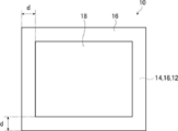
- FIG. 1 is a conceptual view of the gas barrier laminate (gas barrier film) of the present invention as viewed from the surface direction of the main surface.
- FIG. 2 is a plan view of the gas barrier laminate of the present invention.
- the plan view is a view of the gas barrier laminate of the present invention as viewed from the direction orthogonal to the main surface of the support 12.
- the main surface is the largest surface of the sheet (film, plate).
- the area is the area of the main surface unless otherwise noted.
- the gas barrier laminate 10 shown in FIG. 1 is formed on the surface of a support 12, the first organic layer 14 formed on one surface (main surface) of the support 12, and the surface of the first organic layer 14 First inorganic layer 16, the second organic layer 14 formed on the surface of the first inorganic layer 16, and the second layer formed on the surface of the second organic layer 14 It has the inorganic layer 16 and the protective organic layer 18 which is an organic layer most separated from the support 12 and formed on the surface of the second inorganic layer 16.
- the gas barrier laminate of the present invention has an inorganic layer and an organic layer alternately, and in the organic layer and the inorganic layer laminated alternately, it is the organic layer that is most separated from the support.
- the organic layer most separated from the support 12 is the protective organic layer 18.
- the organic layer most distant from the support has a smaller area than the inorganic layer most distant from the support among the inorganic layers.
- the protective organic layer 18 which is the organic layer most separated from the support 12 is the formation surface (lower layer) of the second inorganic layer 16 which is most separated from the support 12, that is, the protective organic layer 18. The area is smaller than that of the inorganic layer 16 of the layer.
- the support 12 side is also referred to as "lower”
- the protective organic layer 18 side as "upper".
- the gas barrier laminate 10 of the illustrated example has, as a preferred embodiment, an organic-inorganic laminate type gas barrier having at least one combination of an inorganic layer 16 exhibiting gas barrier properties and an organic layer 14 serving as a base of the inorganic layer 16. It is a laminate.
- the gas barrier laminate 10 of the illustrated example has two sets of the combination of the inorganic layer 16 and the organic layer 14 to be the base and has the protective organic layer 18 thereon, the present invention There is no limitation.
- the gas barrier laminate of the present invention has one set of the combination of the inorganic layer 16 and the organic layer 14 to be the base, and has the protective organic layer 18 thereon.
- Support 12 ⁇ organic layer 14 ⁇ inorganic layer 16 A layer configuration of the protective organic layer 18 may be used.
- the gas barrier laminate of the present invention has three sets of the combination of the inorganic layer 16 and the organic layer 14 serving as a base, and the protective organic layer 18 thereon, the support 12-organic layer 14-inorganic layer 16
- the layer structure of the organic layer 14, the inorganic layer 16, the organic layer 14, the inorganic layer 16, and the protective organic layer 18 may be used.
- the gas barrier laminate of the present invention may have four or more sets of combinations of the inorganic layer 16 and the organic layer 14 to be a base, and may have the protective organic layer 18 thereon.
- the gas barrier laminate of the present invention may not have the organic layer 14 between the support 12 and the first inorganic layer 16 closest to the support 12. If it is an example of illustration, it is not necessary to have the 1st-layer organic layer 14 used as a foundation
- the gas barrier laminate of the present invention has the inorganic layer and the organic layer alternately on at least one surface side of the support, and among the inorganic layer and the organic layer formed alternately, the support If it is the organic layer that is the most separated, various layer configurations can be used.
- the support 12 may be a known resin-made sheet (film, plate) used as a support in various gas barrier films, various laminated functional films, and the like.
- the material of the support 12 is not limited, and various resin materials can be used as long as the organic layer 14, the inorganic layer 16 and the protective organic layer 18 can be formed.
- the material of the support 12 is, for example, polyethylene (PE), polyethylene naphthalate (PEN), polyamide (PA), polyethylene terephthalate (PET), polyvinyl chloride (PVC), polyvinyl alcohol (PVA), polyacrylonitrile (PAN) ), Polyimide (PI), transparent polyimide, polymethyl methacrylate resin (PMMA), polycarbonate (PC), polyacrylate, polymethacrylate, polypropylene (PP), polystyrene (PS), acrylonitrile butadiene styrene copolymer (ABS) And cyclic olefin copolymer (COC), cycloolefin polymer (COP), and triacetyl cellulose (TAC).
- PE polyethylene
- PEN polyethylene naphthalate
- PA polyamide
- the thickness of the support 12 can be set as appropriate depending on the application, material and the like.
- the thickness of the support 12 is from the viewpoint of sufficiently securing the mechanical strength of the gas barrier laminate 10 and from the viewpoint of securing the flexibility (flexibility) of the gas barrier laminate 10 and reducing the weight and thickness thereof. Therefore, the thickness is preferably 5 to 150 ⁇ m, and more preferably 10 to 100 ⁇ m.
- the support 12 may have a functional layer on its surface.
- the functional layer include a protective layer, a sealing layer, a light reflection layer, an antireflective layer, a light shielding layer, a planarization layer, a buffer layer, and a stress relaxation layer.
- the organic layer 14 and the protective organic layer 18 are layers made of, for example, an organic compound obtained by polymerizing (crosslinking or curing) a monomer, a dimer, an oligomer or the like.
- the organic layer 14 serving as the lower layer of the inorganic layer 16 is the organic layer 14 serving as a base for properly forming the inorganic layer 16.
- the first organic layer 14 formed on the surface of the support 12 embeds the irregularities on the surface of the support 12 and foreign matter attached to the surface, and the surface on which the first inorganic layer 16 is formed To make it possible to properly form the first inorganic layer 16.
- the second organic layer to be the lower layer of the second inorganic layer 16 also exhibits the same function. By having such an organic layer 14 to be a base, it is possible to properly form the inorganic layer 16 that mainly exhibits gas barrier properties.
- the protective organic layer 18 which is the organic layer most separated from the support 12 mainly protects the second inorganic layer 16 most separated from the support 12.
- Organic layer to That is, the protective organic layer 18 is an organic layer for protecting the lower inorganic layer 16.
- the gas barrier laminate 10 of the present invention can prevent damage to the inorganic layer 16 and maintain desired gas barrier properties.
- the protective organic layer 18 is the inorganic layer 16 most separated from the support 12 among the organic layers and the inorganic layers alternately formed, that is, the formation surface of itself. The area is smaller than the lower second inorganic layer 16. This point will be described in detail later.
- the organic layer 14 to be the base of the inorganic layer 16 and the protective organic layer 18 are basically the same. Therefore, the following description will be made with the organic layer 14 as a representative example, unless it is particularly necessary to distinguish.
- the organic layer 14 is formed, for example, by curing a composition for forming an organic layer containing an organic compound (monomer, dimer, trimer, oligomer, polymer and the like).
- the composition for forming an organic layer may contain only one type of organic compound, or may contain two or more types.
- the organic layer 14 contains, for example, a thermoplastic resin and an organic silicon compound.
- the thermoplastic resin is, for example, polyester, (meth) acrylic resin, methacrylic acid-maleic acid copolymer, polystyrene, transparent fluorine resin, polyimide, fluorinated polyimide, polyamide, polyamide imide, polyether imide, cellulose acylate, polyurethane And polyether ether ketone, polycarbonate, alicyclic polyolefin, polyarylate, polyether sulfone, polysulfone, fluorene ring modified polycarbonate, alicyclic modified polycarbonate, fluorene ring modified polyester, and an acrylic compound.
- organosilicon compounds include polysiloxanes.
- the organic layer 14 preferably includes a polymer of a radical curable compound and / or a cationic curable compound having an ether group from the viewpoint of excellent strength and the viewpoint of glass transition temperature.
- the organic layer 14 preferably contains a (meth) acrylic resin whose main component is a polymer such as a monomer or oligomer of (meth) acrylate from the viewpoint of lowering the refractive index of the organic layer 14. By lowering the refractive index, the organic layer 14 has high transparency and improved light transmittance.
- the organic layer 14 is more preferably a difunctional or more functional group such as dipropylene glycol di (meth) acrylate (DPGDA), trimethylolpropane tri (meth) acrylate (TMPTA), dipentaerythritol hexa (meth) acrylate (DPHA), etc.
- DPGDA dipropylene glycol di (meth) acrylate
- TMPTA trimethylolpropane tri (meth) acrylate
- DPHA dipentaerythritol hexa
- (meth) acrylates of (meth) acrylates polymers of (meth) acrylates such as dimers and oligomers, and more preferably polymers of (meth) acrylates of trifunctional or higher functionality such as monomers, dimers and oligomers
- (meth) acrylic resin containing as a main component In addition, a plurality of these (meth) acrylic resins may be used.
- the main component refers to the component
- composition for forming an organic layer preferably contains, in addition to the organic compound, an organic solvent, a surfactant, and a silane coupling agent.
- each organic layer 14 may be the same or different.
- the materials of the organic layer 14 and the protective organic layer 18 may be the same or different.
- the thickness of the organic layer 14 is preferably 0.5 to 5 ⁇ m, and more preferably 1 to 3 ⁇ m.
- the thickness of the organic layer 14 is preferably 0.5 to 5 ⁇ m, and more preferably 1 to 3 ⁇ m.
- each organic layer 14 may be the same or different.
- the organic layer 14 and the protective organic layer 18 may also be the same or different in thickness.
- the organic layer 14 can be formed by a known method depending on the material.
- the organic layer 14 can be formed by a coating method in which the composition for forming an organic layer described above is applied and the composition for forming an organic layer is dried.
- the organic compound in the composition for organic layer formation is polymerized (crosslinked) by further irradiating ultraviolet rays to the dried composition for organic layer formation, if necessary. .
- the organic layer 14 can be formed by so-called roll-to-roll.
- roll to roll is also referred to as "RtoR”.
- RtoR a sheet-like material is sent out from a roll formed by winding a long sheet-like material, film formation is performed while conveying the film-forming target sheet in the longitudinal direction, and the film-formed sheet material is rolled Manufacturing method.
- the inorganic layer 16 is a thin film containing an inorganic compound, and is provided on the surface of the organic layer 14.
- the inorganic layer 16 mainly exhibits gas barrier properties.
- the inorganic layer 16 is properly formed by being provided on the surface of the organic layer 14. For example, there are areas on the surface of the support 12 where it is difficult for an inorganic compound to form a film, such as irregularities and shadows of foreign matter.
- the organic layer 14 By providing the organic layer 14 on the support 12, the region where the inorganic compound is difficult to deposit is covered. Therefore, the inorganic layer 16 can be formed on the entire surface of the support 12 without a gap. In this respect, the same applies to the second and subsequent inorganic layers 16.
- the inorganic compound used for the well-known gas barrier layer which consists of an inorganic compound which expresses gas barrier property can be variously utilized.
- the material of the inorganic layer 16 include metal oxides such as aluminum oxide, magnesium oxide, tantalum oxide, zirconium oxide, titanium oxide and indium tin oxide (ITO); metal nitrides such as aluminum nitride; and metals such as aluminum carbide Carbides; Silicon oxides such as silicon oxide, silicon oxynitride, silicon oxycarbide, silicon oxynitride carbide, etc.
- Silicon nitrides such as silicon nitride and silicon carbonitride; Silicon carbides such as silicon carbide; Hydrides of these; And mixtures thereof, and inorganic compounds such as hydrogen-containing compounds thereof. Also, mixtures of two or more of these are available.
- silicon nitride, silicon oxide, silicon oxynitride, aluminum oxide, and a mixture of two or more of them are suitably used in that they have high transparency and can exhibit excellent gas barrier properties. Above all, silicon nitride is suitably used in that it can exhibit excellent gas barrier properties.
- the thickness of the inorganic layer 16 is preferably 10 to 150 nm, more preferably 12 to 100 nm, and still more preferably 15 to 75 nm. By setting the thickness of the inorganic layer 16 to 10 nm or more, it is preferable in that the inorganic layer 16 which can stably exhibit sufficient gas barrier performance can be formed. In addition, the inorganic layer 16 is generally brittle, and if it is too thick, there is a possibility of cracking, cracking, peeling and the like, but cracking occurs if the thickness of the inorganic layer 16 is 150 nm or less Can be prevented.
- each inorganic layer 16 may be the same or different.
- the inorganic layer 16 can be formed by a known method depending on the material. For example, plasma CVD such as CCP (Capacitively Coupled Plasma) -CVD (Chemical Vapor Deposition) and ICP (Inductively Coupled Plasma) -CVD, atomic layer deposition (ALD (Atomic Layer Deposition)), magnetron sputtering, reactive sputtering, etc. Sputtering and various vapor phase film forming methods such as vacuum evaporation are suitably mentioned.
- the inorganic layer 16 is also formed of RtoR.
- Such a gas barrier laminate 10 of the present invention is preferably suitably used as a substrate for forming an electronic device.
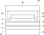
- FIG. 3 an example of the electronic device of this invention which uses the gas barrier laminate 10 of this invention is shown notionally.
- FIG. 3 shows an example in which the electronic device of the present invention is used for an organic electroluminescent lighting device (organic EL (Electro Luminescence) lighting device) as an example.
- the electronic device of the present invention is not limited to the organic EL lighting device 24.
- the electronic device of the present invention may be a solar cell (solar cell device) having a solar cell element instead of the organic EL lighting element 26.
- the electronic device of the present invention includes various known electronic devices such as organic EL devices other than organic EL lighting devices such as organic EL displays, electronic paper, and quantum dot devices using quantum dots. It is available. Above all, the electronic device of the present invention is suitably used for an organic EL lighting device and a solar cell.
- the organic EL lighting device 24 shown in FIG. 3 forms an organic EL lighting element 26 on the surface of the protective organic layer 18 using the above-described gas barrier laminate 10 as a base material, and forms a rectangular frame so as to surround the protective organic layer 18
- the sealing layer 28 is provided, and the sealing base 30 is adhered to the sealing layer 28, whereby the organic EL lighting element 26 is sealed with the sealing base 30.
- the organic EL lighting device 24 may have various members of a known organic EL lighting device (organic EL device), such as a passivation film and a desiccant, as necessary. .
- the sealing base 30 side is also referred to as “upper”, and the support 12 side is also referred to as “lower”.
- the second inorganic layer 16 (the inorganic layer in which the protective organic layer 18 which is the organic layer most separated from the support 12 is the most separated from the support 12)
- the area is smaller than the lower inorganic layer 16) of the protective organic layer 18.
- the protective organic layer 18 is contained in the inorganic layer 16 in the lower layer. Ru.
- the organic EL lighting device 24 forms the organic EL lighting element 26 in the protective organic layer 18.
- the sealing layer 28 is a frame surrounding the protective organic layer 18 and the organic EL lighting element 26, and the sealing base 30 for sealing the organic EL lighting element 26 is placed on the sealing layer 28. Be glued. Therefore, in the illustrated organic EL lighting device 24, the protective organic layer 18 is not exposed to the outside including all the end faces.
- the gas barrier laminate 10 (organic EL lighting device 24) of the present invention suitably prevents the deterioration of the organic EL lighting element 26 due to moisture.
- the protective organic layer protects the lower inorganic layer (the uppermost inorganic layer in the inorganic layer) so that the gas barrier laminate exhibits and maintains predetermined gas barrier properties.
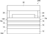
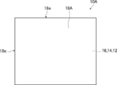
- the protective organic layer 18A is generally formed so as to cover the entire surface of the lower inorganic layer 16. Therefore, as shown in FIG. 6, the organic EL lighting device 24A using the conventional gas barrier laminate as a base material forms a frame-like sealing layer 28 on the protective organic layer 18A, and the sealing layer 28 is formed. By bonding the sealing base 30, the organic EL lighting element 26 is sealed by the sealing base 30. Therefore, in the conventional organic EL lighting device 24A, the end face 18e of the protective organic layer 18A is exposed to the outside.
- the protective organic layer 18A is for protecting the underlying inorganic layer 16.
- the inorganic layer 16 is, for example, a thin and hard film having a thickness of about 10 to 150 nm.
- the protective organic layer 18A needs to have a certain degree of hardness.
- the organic layer (layer made of an organic material) having a hardness that can sufficiently protect the thin and hard inorganic layer 16 does not have sufficient gas barrier properties. Therefore, in the conventional gas barrier laminate 10A in which the end face 18e of the protective organic layer 18A is exposed to the outside, moisture intrudes from the end face 18e of the protective organic layer 18A and reaches the organic EL lighting element 26.
- the protective organic layer 18A Without the protective organic layer 18A, the deterioration of the organic EL lighting element 26 due to moisture entering from the end face of the protective organic layer 18A can be prevented.
- the protective organic layer 18A when the protective organic layer 18A is not present, the inorganic layer 16 is exposed at the outermost surface, so when, for example, it is wound into a roll, it is cut into a predetermined shape, and in handling etc. The layer 16 is damaged, and the gas barrier laminate does not exhibit predetermined gas barrier properties.
- the area of the protective organic layer 18 is smaller than that of the lower inorganic layer 16.
- the protective organic layer 18 is included in the lower inorganic layer 16.
- various adhesives can be selected as the adhesive for forming the sealing layer 28 having sufficient gas barrier properties. Therefore, according to the gas barrier laminate 10 of the present invention, as shown in FIG. 3, the end face of the protective organic layer 18 is inside the sealing layer 28, and preferably, the protective organic layer 18 is preferably an inorganic layer 16 of the lower layer. , And can be enclosed by the sealing layer 28 and the sealing base 30.
- the organic EL lighting element 26 by moisture entering from the end face of the protective organic layer 18 Of the organic EL lighting device (electronic device) can be extended.
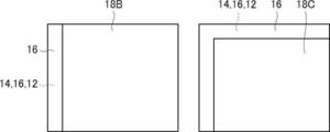
- the protective organic layer 18 is included in the lower inorganic layer 16 in a plan view.
- the present invention is not limited thereto, and the protective organic layer 18 is smaller than the lower inorganic layer 16, and a part of the end face of the protective organic layer 18 is in the surface direction than the end face of the lower inorganic layer 16. It should be located inside. That is, in the gas barrier laminate 10 of the present invention, for example, as in a protective organic layer 18B shown on the left side of FIG. 4, only one end face may be positioned inside the end face of the lower inorganic layer 16 Alternatively, as in a protective organic layer 18C shown on the right side of FIG.
- the number of the end faces of the protective organic layer exposed to the outside be small. Therefore, in the gas barrier laminate of the present invention, as in the rectangular protective organic layer 18C shown on the right side of FIG. 4, the end faces (50% or more of all the end faces) of at least two sides of the protective organic layer
- the protective organic layer 18 is included in the lower inorganic layer 16 in the plan view as shown in FIGS. 1 and 2, that is, all the end faces of the protective organic layer 18. Is more preferably positioned inside the end face of the lower inorganic layer 16.
- a sealing layer so that the end face (50% or more of all the end faces) of at least two sides of the protective organic layer is inside in the surface direction. It is more preferable to provide the sealing layer 28 so as to surround the protective organic layer 18 in the plane direction as described above, and seal with the sealing base 30.
- the distance d between the end face of the protective organic layer 18 and the end face of the lower inorganic layer 16 there is no limit to Here, from the viewpoint of preventing the deterioration of the organic EL lighting element 26 caused by the moisture entering from the end face of the protective organic layer 18, the thickness (size in the surface direction) of the sealing layer 28 up to the protective organic layer 18 can be increased. In terms of point, it is preferable that the distance d between the end face of the protective organic layer 18 and the end face of the lower inorganic layer 16 be longer.
- the distance d between the end face of the protective organic layer 18 and the end face of the lower inorganic layer 16 is long, the area not covered by the protective organic layer 18 in the inorganic layer 16 increases, and the inorganic layer 16 is prone to damage.
- the distance d between the end face of the protective organic layer 18 and the end face of the lower inorganic layer 16 in at least a part of the end face preferably in an area of 50% or more in the plane direction Is preferably 1 to 10 mm, more preferably 1 to 8 mm, and still more preferably 1 to 7 mm.
- the sealing layer 28 is for bonding the sealing base 30 and sealing the organic EL lighting element 26 by the sealing base 30.
- the sealing substrate 30 is provided on the side of the organic EL lighting element 26 opposite to the protective organic layer 18. Specifically, in the organic EL lighting device 24, the organic EL lighting element 26 is sealed by the sealing base 30, the sealing layer 28, and the gas barrier laminate 10.
- the sealing layer 28 can be variously used as a sealing layer, a pressure-sensitive adhesive layer, and the like in a known organic EL device.
- a UV curable resin is preferable as the material of the sealing layer 28, and more specifically, a UV curable epoxy resin, a UV curable acrylate resin, and the like are exemplified.
- a commercially available adhesive can also be used suitably for the sealing layer 28, For example, XNR5516 by Nagase ChemteX Corp. etc. is illustrated.
- an adhesive sheet or an adhesive tape may be used as the sealing layer 28. Adhesive sheets and adhesive tapes, including commercial products, are widely available as what is known as OCA (Optical Clear Adhesive).
- the sealing layer 28 is provided in a frame shape surrounding the protective organic layer 18 (organic EL lighting element 26), and the region where the organic EL lighting element 26 is present is a space.
- the invention is not limited to this. That is, in the organic EL lighting device (electronic device), the space between the organic EL lighting element 26, the protective organic layer 18, the inorganic layer 16 under the protective organic layer 18, and the sealing base 30 is filled with the sealing layer It may be configured as described above. However, in terms of the optical characteristics of the organic EL lighting device 24 and the flexibility of the organic EL lighting device 24, the sealing layer 28 has a frame shape surrounding the protective organic layer 18, and the area where the organic EL lighting element 26 is present is a space. The configuration of FIG. 3 is more advantageous.
- the sealing layer 28 has a frame shape surrounding the protective organic layer 18, the distance d between the end face of the protective organic layer 18 and the end face of the inorganic layer 16 in the lower layer and the thickness of the sealing layer 28 ( Depending on the size in the surface direction, the sealing layer 28 may cover the end in the surface direction of the protective organic layer 18.
- the sealing layer 28 preferably has high gas barrier properties.
- the material of the sealing layer 28 has a water vapor transmission rate per 500 ⁇ m (water vapor transmission coefficient per 500 ⁇ m) of 1 ⁇ 10 ⁇ 1 to 1 ⁇ 10 ⁇ 3 g / (m 2 ⁇ day) Is more preferable, and 1 ⁇ 10 ⁇ 2 to 1 ⁇ 10 ⁇ 3 g / (m 2 ⁇ day) is more preferable.
- the sealing layer 28 preferably has a water vapor transmission rate of 1 ⁇ 10 ⁇ 1 to 1 ⁇ 10 ⁇ 3 g / (m 2 ⁇ day), and 1 ⁇ 10 ⁇ 2 to 1 ⁇ 10 ⁇ 3 g / (m 2 ⁇ day) is more preferred.
- the water vapor transmission rate of the sealing layer 28 as referred to herein means protection from the end face outside the sealing layer 28. It is the water vapor transmission rate of the sealing layer 28 in the thickness to the end face of the organic layer 18.
- the water vapor transmission rate of the sealing layer 28 means the thickness of the sealing layer 28 It is the water vapor transmission rate of the sealing layer 28 when it is regarded as from the outer end face of the sealing layer 28 to the end face of the protective organic layer 18.
- the sealing layer 28 has lower gas barrier properties than the sealing base 30 and the inorganic layer 16. Therefore, from the viewpoint of preventing the deterioration of the organic EL lighting element 26 due to moisture, it is advantageous that the height of the sealing layer 28 (the size in the vertical direction, that is, the direction orthogonal to the surface direction) be smaller. On the other hand, in order to apply the sealing layer 28 uniformly and seal the organic EL lighting element 26 precisely, it is preferable that the sealing layer 28 have a certain height. Specifically, the height of the sealing layer 28 is preferably 1 to 500 ⁇ m, more preferably 50 to 400 ⁇ m, and still more preferably 100 to 300 ⁇ m.
- the organic EL lighting element 26 is a known organic EL lighting element used for an organic EL lighting device (organic EL lighting device).
- the organic EL lighting element 26 includes an anode, a hole injection layer (hole injection layer), a hole transport layer (hole transport layer), a light emitting layer, a hole blocking layer (hole blocking layer), an electron transport layer,
- the sealing substrate 30 is also a known sealing substrate used for a known organic EL lighting device. Specifically, a sheet-like material made of yttria-stabilized zirconia (YSZ), glass (alkali-free glass, soda lime glass, etc.), etc. is exemplified.
- a gas barrier film formed by forming a gas barrier layer made of an inorganic compound on a resin film can also be suitably used. Examples of the gas barrier layer include a silicon nitride layer, a silicon oxide layer, a silicon oxynitride layer, and an aluminum oxide layer.
- the gas barrier layer side is directed to the organic EL lighting element 26, and sealing with the sealing base 30 is performed.
- the sealing substrate 30 includes one or more combinations of the same inorganic layer that exhibits gas barrier properties as the gas barrier laminate 10 shown in FIG. 1 and an organic layer that is a base of the inorganic layer.
- An organic-inorganic laminate type gas barrier film is also suitably usable.
- the organic-inorganic laminate type gas barrier film usually has a protective organic layer for protecting the inorganic layer by covering the uppermost inorganic layer as a layer most separated from the support.
- the gas barrier laminate of the present invention can also be used more suitably as illustrated in FIG. 5 to conceptually illustrate the gas barrier laminate 10.
- FIG. 5 to conceptually illustrate the gas barrier laminate 10.
- the sealing layer 28 is provided in a frame shape surrounding the protective organic layer 18, and the organic EL lighting device in which the area where the organic EL lighting element 26 exists is a space.
- the gas barrier film of the present invention is not the ordinary organic-inorganic laminated gas barrier film having a protective organic layer. It is preferable to use a gas barrier laminate or an organic-inorganic laminate type gas barrier film not having a protective organic layer.
- a support 12 such as a PET film is prepared, and the first organic layer 14 is formed on one surface of the support 12 by the coating method using the composition for forming an organic layer as described above.
- coating of the composition for organic layer formation can utilize well-known methods, such as the bar-coating method, the gravure coat method, and the die-coating method.
- the first inorganic layer 16 is formed on the surface of the first organic layer 14 by plasma CVD such as CCP-CVD.
- the protective organic layer 18 is formed similarly to the following.
- the second organic layer 14 and the second inorganic layer 16 are formed.
- the formation of the same organic layer 14 and the inorganic layer 16 may be repeated.
- a composition for forming the protective organic layer 18 (a composition for forming a protective organic layer) is applied to the entire surface of the inorganic layer 16 of the second layer (uppermost layer), and an organic layer is similarly formed.
- the formation of each of these layers preferably uses RtoR, as described above.
- the laminate prepared as necessary is cut into a predetermined shape, and then the periphery of the organic layer formed on the second inorganic layer 16 of the laminate is removed, and the inorganic material of the lower layer in the plan view is removed.
- the protective organic layer 18 included in the layer 16 is formed to obtain the gas barrier laminate 10 of the present invention.
- known methods can be used, but preferably etching is used. Although both dry etching and wet etching can be used as the etching, dry etching is preferably used in that the adhesion between the inorganic layer 16 and the sealing layer 28 can be improved.
- Dry etching is a method of etching a material by reactive gas, ions, radicals or the like.
- dry etching known methods such as plasma etching, ion etching, and focused ion beam etching can be used.
- Ion etching is a method of etching a solid surface with helium (He), argon (Ar), neon (Ne), an inert gas containing a combination thereof, or the like.
- Reactive ion etching RIE (Reactive Ion Etching)
- RIE Reactive Ion Etching
- the composition for forming an organic layer is applied to the entire surface of the inorganic layer 16, and the protective organic layer 18 is not formed by removing the periphery by etching.
- the composition for forming an organic layer may be applied so as to be included in the inorganic layer 16 in the figure to form the protective organic layer 18.
- an anode, a hole injection layer, a hole transport layer, a light emitting layer, a hole blocking layer, an electron transport layer, an electron injection layer, a cathode, etc. on the protective organic layer 18 To form the organic EL lighting element 26.
- an adhesive serving as the sealing layer 28 is applied in a frame shape to the exposed peripheral portion of the inorganic layer 16 under the protective organic layer 18.
- the sealing substrate 30 is laminated on the adhesive, and then the adhesive is cured by, for example, irradiation with ultraviolet light, and the inorganic layer 16 (gas barrier laminate 10) and the sealing substrate are sealed by the sealing layer 28
- the organic EL lighting device 24 is manufactured by bonding 30.
- Example 1 ⁇ Production of gas barrier laminate> As a support, a PET film (A4300, manufactured by Toyobo Co., Ltd.) having a thickness of 100 ⁇ m was prepared.
- the composition for organic layer formation for forming an organic layer was prepared.
- the solid content concentration of the composition for forming an organic layer was 15% by mass.
- the prepared composition for forming an organic layer was applied to the surface of the prepared support. The coating was performed using a die coater such that the film thickness of the organic layer was 1 ⁇ m. After application, it was dried in an oven at 80 ° C. for 3 minutes.
- the composition for forming an organic layer is cured by irradiating the ultraviolet rays of a high pressure mercury lamp (accumulated irradiation amount: about 600 mJ / cm 2 ) in a chamber in which the oxygen concentration is 0.1% by a nitrogen substitution method. A layer was formed.
- a silicon nitride film having a thickness of 40 nm was formed as an inorganic layer.
- the formation of the inorganic layer was performed using a CCP-CVD apparatus (manufactured by Samco).
- As raw material gases silane gas (flow rate 160 sccm: 0 ° C., standard condition at 1 atm, and so forth), ammonia gas (flow rate 370 sccm), hydrogen gas (flow rate 590 sccm), and nitrogen gas (flow rate 240 sccm) were used.
- the deposition pressure was 40 Pa.
- the power supply was a high frequency power supply with a frequency of 13.56 MHz, and the plasma excitation power was 2.5 kW.
- the organic layer between the support and the inorganic layer (the first inorganic layer) is also referred to as a base organic layer.
- An organic layer to be a protective organic layer having a thickness of 1.5 ⁇ m was formed on the inorganic layer using the prepared composition for forming a protective organic layer in the same manner as the organic layer formed above.
- a laminate having an organic layer, an inorganic layer, and an organic layer to be a protective organic layer formed on the surface of a support was produced.
- the laminate was cut into 50 ⁇ 50 mm. Thereafter, the entire peripheral portion (all four sides) of the organic layer to be a protective organic layer was removed by etching by 1 mm in a plane direction to form a protective organic layer.
- Two gas barrier laminates were prepared.
- the water vapor transmission rate of the manufactured gas barrier laminate was measured by the calcium corrosion method (the method described in JP-A-2005-283561). As a result, the water vapor transmission rate of the laminate was 1 ⁇ 10 ⁇ 6 g / (m 2 ⁇ day).
- a polyethylenedioxythiophene-polystyrene sulfonic acid (PEDOT-PSS) electrode (anode) was formed to a thickness of 80 nm on the surface of one protective organic layer of the produced gas barrier laminate.
- a molybdenum oxide (MoO 3 ) layer of 2 nm is formed as a hole injection layer on the surface of the formed anode as a hole injection layer, and a hole transport layer ( ⁇ -NPD: Bis [) is sequentially formed on the surface of the molybdenum oxide layer.
- LiF lithium fluoride
- aluminum 1.5 nm
- silver 15 nm
- An organic EL lighting element was formed.
- An adhesive (XNR 5516, manufactured by Nagase ChemteX Corp.) was applied in a frame shape on the periphery of the upper surface (the surface on the protective organic layer side) of the gas barrier laminate in which the organic EL lighting element was formed.
- the adhesive cures, the water vapor transmission rate per 500 ⁇ m is 1 ⁇ 10 ⁇ 1 g / (m 2 ⁇ day).
- the other gas barrier laminate was used as a sealing base material, and the end portion was aligned with the upper surface side facing the organic EL lighting element side and laminated.
- the adhesive was cured to form a sealing layer by irradiating ultraviolet rays of a high pressure mercury lamp (total irradiation amount: approximately 6 J / cm 2 ).
- the organic EL lighting element is sealed by bonding the gas barrier laminate in which the organic EL lighting element is formed and the sealing base (the same gas barrier laminate) with a sealing layer, as shown in FIG.
- An EL lighting device was manufactured.
- the height (size in the vertical direction) of the formed sealing layer was 500 ⁇ m, and the thickness (size in the surface direction) of the sealing layer was 5 mm.
- a 4 mm sealing layer covers the end of the protective organic layer.
- Example 2 and Example 3 In the production of one gas barrier laminate, etching of the peripheral portion of the organic layer to be a protective organic layer is performed on two adjacent sides (see Example 2, right side in FIG. 4) and one side (Examples 3, 4) A gas barrier laminate was produced in the same manner as in Example 1 except that the left side was referred to). An organic EL lighting device was produced in the same manner as in Example 1 except that the organic EL lighting element was formed on the gas barrier laminate.
- the gas barrier laminate used as a sealing base material is the same as Example 1. About this point, it is the same as that of all the examples which changed the composition of the gas barrier layered product which forms an organic EL lighting element. Therefore, in Example 2, the end faces of the two sides are exposed to the outside in the protective organic layer of the gas barrier laminate in which the organic EL lighting element is formed, and in Example 3, the end faces of the three sides are exposed to the outside It has become.
- Example 4 In the preparation of one gas barrier laminate, the etching width of the peripheral part of the organic layer to be the protective organic layer is changed to 0.5 mm, 7 mm, 8 mm, 10 mm and 11 mm, and the end face of the protective organic layer and the lower layer Distance to the end face of the inorganic layer (distance d in FIGS. 1 and 2) is 0.5 mm (Example 4), 7 mm (Example 5), 8 mm (Example 6), 10 mm (Example 7), And, a gas barrier laminate was produced in the same manner as in Example 1 except that it was changed to 11 mm (Example 8). An organic EL lighting device was produced in the same manner as in Example 1 except that the organic EL lighting element was formed on the gas barrier laminate.
- Example 9 A gas barrier laminate was produced in the same manner as in Example 1 except that in the production of one gas barrier laminate, the organic layer (underlying organic layer) between the support and the inorganic layer was not formed. That is, this gas barrier laminate has a layer configuration of a support, an inorganic layer, and a protective organic layer.
- An organic EL lighting device was produced in the same manner as in Example 1 except that the organic EL lighting element was formed on the gas barrier laminate.
- Example 10 In the preparation of one gas barrier laminate, after forming the second organic layer, the second inorganic layer is formed on the surface of the second organic layer in the same manner as the first inorganic layer, The same as Example 1 except that the third organic layer was formed on the surface of the second inorganic layer in the same manner as the second organic layer, and the third organic layer was a protective organic layer.
- a gas barrier laminate was produced. That is, this gas barrier laminate has a layer structure of a support, an organic layer, an inorganic layer, an organic layer, an inorganic layer, and a protective organic layer.
- An organic EL lighting device was produced in the same manner as in Example 1 except that an organic EL lighting element was formed on the gas barrier laminate, and the height of the sealing layer was set to 300 ⁇ m.
- the sealing layer has a height of 0.5 ⁇ m (Example 11), 600 ⁇ m (Example 12), 50 ⁇ m (Example 13), 400 ⁇ m (Example 14), 100 ⁇ m (Example 15), and 300 ⁇ m (Examples)
- a gas barrier laminate was produced in the same manner as in Example 1 except that the example was changed to 16).
- An organic EL lighting device was produced in the same manner as in Example 1 except that this gas barrier laminate was used.
- Comparative Example 1 In the preparation of one gas barrier laminate, a gas barrier laminate was prepared in the same manner as in Example 1 except that the periphery of the organic layer to be the protective organic layer was not etched. An organic EL lighting device was produced in the same manner as in Example 1 except that the organic EL lighting element was formed on the gas barrier laminate. Therefore, all the edge parts of four sides of the protective organic layer of the gas barrier laminate in which the organic EL lighting element is formed are exposed to the outside.
- Evaluation of the produced organic electroluminescent illuminating device was performed as follows.
- the prepared organic EL lighting device is left in an environment of temperature 60 ° C. and relative humidity 90% RH for 100 hours, and the total area [%] of dark spots with respect to the total light emitting area (area of organic EL lighting element) is shown in the table below. Shown in.
- the gas barrier laminate of the present invention in which the protective organic layer is smaller than the lower inorganic layer and the end face of at least one side is inward in the plane direction from the sealing layer and According to the organic EL lighting device, it has higher high temperature and high humidity durability than that of Comparative Example 1 in which all the end faces of the four sides of the protective organic layer are exposed to the outside, that is, the gas barrier of the gas barrier laminate Sex is excellent.
- Example 1 and Examples 5 to 7 by setting the distance between the end face of the protective organic layer and the end face of the lower inorganic layer in the range of 1 to 10 mm, higher temperature and high humidity durability, ie, better The gas barrier properties of the gas barrier laminate can be obtained.
- Example 8 since the distance between the end face of the protective organic layer and the end face of the lower inorganic layer is 11 mm, which is slightly longer than in Example 7, the inorganic layer is slightly removed during handling before sealing. It is considered that there were more dark spots than in Example 7 due to a lot of damage.
- Example 9 From the comparison between Example 9 and Example 1, by providing the organic layer (underlying organic layer) between the support and the first inorganic layer, good high temperature and high humidity durability, that is, the gas barrier of the gas barrier laminate is obtained. Sex is obtained. Furthermore, as shown in Examples 13 to 16, by setting the height of the sealing layer in the range of 50 to 400 ⁇ m, in particular in the range of 100 to 300 ⁇ m, the high temperature high humidity durability, ie, more excellent. The gas barrier properties of the gas barrier laminate can be obtained. In addition, as shown in Example 10, the height of the sealing layer is in the range of 100 to 300 ⁇ m, and the combination of the organic layer serving as the base and the inorganic layer is two sets (two inorganic layers). Thus, the very high temperature and high humidity durability, that is, the gas barrier properties of the gas barrier laminate can be obtained. From the above results, the effects of the present invention are clear.
Landscapes
- Physics & Mathematics (AREA)
- Condensed Matter Physics & Semiconductors (AREA)
- Electromagnetism (AREA)
- General Physics & Mathematics (AREA)
- Engineering & Computer Science (AREA)
- Computer Hardware Design (AREA)
- Microelectronics & Electronic Packaging (AREA)
- Power Engineering (AREA)
- Electroluminescent Light Sources (AREA)
- Laminated Bodies (AREA)
- Photovoltaic Devices (AREA)
Abstract
Provided are: a gas barrier laminate which is capable of preventing deterioration of an electronic device due to moisture; and an electronic device which uses this gas barrier laminate. A gas barrier laminate according to the present invention comprises: a supporting body; and one or more inorganic layers and one or more organic layers, which are alternately laminated on the supporting body. Among the alternately laminated inorganic layers and organic layers, an organic layer is positioned most distant from the supporting body, and this organic layer positioned most distant from the supporting body has a smaller area than an inorganic layer that is positioned most distant from the supporting body among the inorganic layers.
Description
本発明は、ガスバリア積層体、および、このガスバリア積層体を用いる電子デバイスに関する。
The present invention relates to a gas barrier laminate and an electronic device using the gas barrier laminate.
有機エレクトロルミネッセンス材料(有機EL(Electro Luminescence)材料)を用いる有機ELデバイス、および、太陽電池デバイス等の電子デバイスが、各種の用途に利用されている。
BACKGROUND ART Organic EL devices using organic electroluminescent materials (organic EL (Electro Luminescence) materials) and electronic devices such as solar cell devices are used for various applications.
有機ELデバイス等の電子デバイスは、基材として、ガラス板および金属板等を用いている。しかしながら、近年では、電子デバイスにも、可撓性(フレキシブル性)が要求されている。
一方で、電子デバイスは、一般的に、水分に弱い。特に、有機ELデバイスおよび太陽電池デバイス、中でも特に有機ELデバイスは、非常に水分に弱い。
そのため、可撓性を要求される電子デバイスでは、ガスバリアフィルムを利用してモジュール化することが行われている。 An electronic device such as an organic EL device uses a glass plate, a metal plate or the like as a substrate. However, in recent years, flexibility has also been required for electronic devices.
On the other hand, electronic devices are generally sensitive to moisture. In particular, organic EL devices and solar cell devices, especially organic EL devices, are very sensitive to moisture.
Therefore, in electronic devices that require flexibility, modularization is performed using gas barrier films.
例えば、特許文献1には、基板、有機電界発光素子、および、ガスバリアフィルムを、この順で有し、基板とガスバリアフィルムとを封止層で接着することによって、有機電界発光素子が封止された有機電界発光装置が記載されている。
この有機電界発光装置に記載されるガスバリアフィルムは、支持体(基材フィルム)と、少なくとも1層の無機層を含むバリア層とを有し、バリア層が支持体に対して有機電界発光素子側に位置し、さらに、封止層とバリア層との間にバリア保護層を有する。 For example, Patent Document 1 includes a substrate, an organic electroluminescent device, and a gas barrier film in this order, and the organic electroluminescent device is sealed by bonding the substrate and the gas barrier film with a sealing layer. An organic electroluminescent device is described.
The gas barrier film described in the organic electroluminescent device has a support (base film) and a barrier layer containing at least one inorganic layer, and the barrier layer is on the organic electroluminescent element side with respect to the support And a barrier protective layer between the sealing layer and the barrier layer.
特許文献1に記載される有機電界発光装置のように、ガスバリアフィルムを用いてモジュール化することにより、水分による有機EL素子等の劣化を防止できる。
しかしながら、ガスバリアフィルムを用いてモジュール化した電子デバイスであっても、電子デバイスの構成、使用環境、および、ガスバリアフィルムの構成等によっては、水分による有機EL素子等の劣化を、十分に防止できない場合も多い。 Like the organic electroluminescent device described in Patent Document 1, modularization using a gas barrier film can prevent deterioration of the organic EL element and the like due to moisture.
However, even if it is an electronic device modularized using a gas barrier film, depending on the configuration of the electronic device, the use environment, the configuration of the gas barrier film, etc., deterioration of the organic EL element due to moisture can not be sufficiently prevented. There are also many.
本発明の目的は、このような問題点を解決することにあり、電子デバイスに用いることにより、水分による電子デバイスの劣化を好適に防止できるガスバリア積層体、および、このガスバリア積層体を用いる電子デバイスを提供することにある。
An object of the present invention is to solve such problems, and by using it for an electronic device, a gas barrier laminate capable of suitably preventing the deterioration of the electronic device due to moisture, and an electronic device using this gas barrier laminate To provide.
本発明は、以下の構成によって課題を解決する。
[1] 支持体と、支持体の一方の面側に交互に積層される無機層および有機層と、を有し、
1層以上の無機層および1層以上の有機層を有し、交互に積層される無機層および有機層のうち、支持体と最も離間するのが有機層であり、
支持体と最も離間する有機層は、支持体と最も離間する無機層よりも、面積が小さいことを特徴とするガスバリア積層体。
[2] 支持体の主面と直交する方向から見た際に、支持体と最も離間する有機層が、支持体と最も離間する無機層に内包される、[1]に記載のガスバリア積層体。
[3] 無機層と、無機層の下地となる有機層との組み合わせを、1組以上有する、[1]または[2]に記載のガスバリア積層体。
[4] 無機層を2層以上有する、[1]~[3]のいずれかに記載のガスバリア積層体。
[5] 支持体が樹脂フィルムである、[1]~[4]のいずれかに記載のガスバリア積層体。
[6] 少なくとも一部において、支持体と最も離間する有機層の端面と、支持体と最も離間する無機層の端面との距離が、1~10mmである、[1]~[5]のいずれかに記載のガスバリア積層体。
[7] [1]~[6]のいずれかに記載のガスバリア積層体と、
ガスバリア積層体の支持体と最も離間する有機層の上に形成される電子素子と、
電子素子のうち支持体と最も離間する有機層とは反対側に設けられ、電子素子を封止する封止基材と、
封止基材およびガスバリア積層体を接着する封止層と、を有することを特徴とする電子デバイス。
[8] 封止層の高さが1~500μmである、[7]に記載の電子デバイス。
[9] 封止基材が、[1]~[6]のいずれかに記載のガスバリア積層体である、[7]または[8]に記載の電子デバイス。
[10] 有機エレクトロルミネッセンスデバイス、または、太陽電池デバイスである、[7]~[9]のいずれかに記載の電子デバイス。
[11] 有機エレクトロルミネッセンスデバイスが有機エレクトロルミネッセンス照明装置である、[10]に記載の電子デバイス。 The present invention solves the problems by the following configurations.
[1] It has a support, and an inorganic layer and an organic layer alternately laminated on one side of the support,
Among the inorganic layers and the organic layers which have one or more inorganic layers and one or more organic layers and are alternately stacked, the organic layer is the most distant from the support,
A gas barrier laminate characterized in that the organic layer which is most separated from the support is smaller in area than the inorganic layer which is most separated from the support.
[2] The gas barrier laminate according to [1], wherein the organic layer most separated from the support is included in the inorganic layer most separated from the support when viewed from the direction orthogonal to the main surface of the support .
[3] The gas barrier laminate according to [1] or [2], having one or more combinations of an inorganic layer and an organic layer to be a base of the inorganic layer.
[4] The gas barrier laminate according to any one of [1] to [3], having two or more inorganic layers.
[5] The gas barrier laminate according to any one of [1] to [4], wherein the support is a resin film.
[6] Any one of [1] to [5], wherein the distance between the end face of the organic layer most separated from the support and the end face of the inorganic layer most separated from the support is 1 to 10 mm at least in part The gas barrier laminate as described in.
[7] The gas barrier laminate according to any one of [1] to [6],
An electronic device formed on the support of the gas barrier laminate and the organic layer most separated therefrom;
A sealing base provided on the opposite side of the electronic element from the support and the organic layer most separated from the support and sealing the electronic element;
And a sealing layer for bonding the sealing substrate and the gas barrier laminate.
[8] The electronic device according to [7], wherein the height of the sealing layer is 1 to 500 μm.
[9] The electronic device according to [7] or [8], wherein the sealing substrate is the gas barrier laminate according to any one of [1] to [6].
[10] The electronic device according to any one of [7] to [9], which is an organic electroluminescent device or a solar cell device.
[11] The electronic device according to [10], wherein the organic electroluminescent device is an organic electroluminescent lighting device.
本発明によれば、電子デバイスに用いることにより、水分による電子デバイスの劣化を好適に防止できるガスバリア積層体、および、水分による劣化を防止できる電子デバイスを得ることができる。
ADVANTAGE OF THE INVENTION According to this invention, by using for an electronic device, the gas-barrier laminated body which can prevent deterioration of the electronic device by a water | moisture content suitably, and the electronic device which can prevent deterioration by a water | moisture content can be obtained.
以下、本発明のガスバリア積層体および電子デバイスの実施形態について、図面に基づいて説明する。
Hereinafter, embodiments of the gas barrier laminate and the electronic device of the present invention will be described based on the drawings.
(ガスバリア積層体)
図1および図2に、本発明のガスバリア積層体の一例を概念的に示す。
図1は、本発明のガスバリア積層体(ガスバリアフィルム)を主面の面方向から見た概念図である。図2は、本発明のガスバリア積層体の平面図である。平面図とは、本発明のガスバリア積層体を、支持体12の主面と直交する方向から見た図である。
主面とは、シート状物(フィルム、板状物)の最大面である。また、本発明において、特に断りがない場合には、面積とは、主面の面積である。 (Gas barrier laminate)
1 and 2 schematically show an example of the gas barrier laminate of the present invention.
FIG. 1 is a conceptual view of the gas barrier laminate (gas barrier film) of the present invention as viewed from the surface direction of the main surface. FIG. 2 is a plan view of the gas barrier laminate of the present invention. The plan view is a view of the gas barrier laminate of the present invention as viewed from the direction orthogonal to the main surface of thesupport 12.
The main surface is the largest surface of the sheet (film, plate). In the present invention, the area is the area of the main surface unless otherwise noted.
図1および図2に、本発明のガスバリア積層体の一例を概念的に示す。
図1は、本発明のガスバリア積層体(ガスバリアフィルム)を主面の面方向から見た概念図である。図2は、本発明のガスバリア積層体の平面図である。平面図とは、本発明のガスバリア積層体を、支持体12の主面と直交する方向から見た図である。
主面とは、シート状物(フィルム、板状物)の最大面である。また、本発明において、特に断りがない場合には、面積とは、主面の面積である。 (Gas barrier laminate)
1 and 2 schematically show an example of the gas barrier laminate of the present invention.
FIG. 1 is a conceptual view of the gas barrier laminate (gas barrier film) of the present invention as viewed from the surface direction of the main surface. FIG. 2 is a plan view of the gas barrier laminate of the present invention. The plan view is a view of the gas barrier laminate of the present invention as viewed from the direction orthogonal to the main surface of the
The main surface is the largest surface of the sheet (film, plate). In the present invention, the area is the area of the main surface unless otherwise noted.
図1に示すガスバリア積層体10は、支持体12と、支持体12の一方の表面(主面)に形成される1層目の有機層14と、1層目の有機層14の表面に形成される1層目の無機層16と、1層目の無機層16の表面に形成される2層目の有機層14と、2層目の有機層14の表面に形成される2層目の無機層16と、2層目の無機層16の表面に形成される、支持体12と最も離間する有機層である保護有機層18と、を有する。
本発明のガスバリア積層体は、無機層と有機層とを交互に有し、また、交互に積層される有機層と無機層とにおいて、支持体から最も離間するのは有機層である。図示例においては、交互に積層される有機層と無機層とにおいて、支持体12と最も離間する有機層は、保護有機層18である。
また、支持体から最も離間する有機層は、無機層の中で最も支持体と離間する無機層よりも、面積が小さい。図示例においては、支持体12と最も離間する有機層である保護有機層18は、支持体12と最も離間する2層目の無機層16すなわち保護有機層18の形成面(下層)となる2層目の無機層16よりも、面積が小さい。
なお、本発明のガスバリア積層体では、支持体12側を『下』、保護有機層18側を『上』とも言う。 Thegas barrier laminate 10 shown in FIG. 1 is formed on the surface of a support 12, the first organic layer 14 formed on one surface (main surface) of the support 12, and the surface of the first organic layer 14 First inorganic layer 16, the second organic layer 14 formed on the surface of the first inorganic layer 16, and the second layer formed on the surface of the second organic layer 14 It has the inorganic layer 16 and the protective organic layer 18 which is an organic layer most separated from the support 12 and formed on the surface of the second inorganic layer 16.
The gas barrier laminate of the present invention has an inorganic layer and an organic layer alternately, and in the organic layer and the inorganic layer laminated alternately, it is the organic layer that is most separated from the support. In the illustrated example, in the alternately laminated organic layer and the inorganic layer, the organic layer most separated from thesupport 12 is the protective organic layer 18.
In addition, the organic layer most distant from the support has a smaller area than the inorganic layer most distant from the support among the inorganic layers. In the illustrated example, the protectiveorganic layer 18 which is the organic layer most separated from the support 12 is the formation surface (lower layer) of the second inorganic layer 16 which is most separated from the support 12, that is, the protective organic layer 18. The area is smaller than that of the inorganic layer 16 of the layer.
In the gas barrier laminate of the present invention, thesupport 12 side is also referred to as "lower", and the protective organic layer 18 side as "upper".
本発明のガスバリア積層体は、無機層と有機層とを交互に有し、また、交互に積層される有機層と無機層とにおいて、支持体から最も離間するのは有機層である。図示例においては、交互に積層される有機層と無機層とにおいて、支持体12と最も離間する有機層は、保護有機層18である。
また、支持体から最も離間する有機層は、無機層の中で最も支持体と離間する無機層よりも、面積が小さい。図示例においては、支持体12と最も離間する有機層である保護有機層18は、支持体12と最も離間する2層目の無機層16すなわち保護有機層18の形成面(下層)となる2層目の無機層16よりも、面積が小さい。
なお、本発明のガスバリア積層体では、支持体12側を『下』、保護有機層18側を『上』とも言う。 The
The gas barrier laminate of the present invention has an inorganic layer and an organic layer alternately, and in the organic layer and the inorganic layer laminated alternately, it is the organic layer that is most separated from the support. In the illustrated example, in the alternately laminated organic layer and the inorganic layer, the organic layer most separated from the
In addition, the organic layer most distant from the support has a smaller area than the inorganic layer most distant from the support among the inorganic layers. In the illustrated example, the protective
In the gas barrier laminate of the present invention, the
図示例のガスバリア積層体10は、好ましい態様として、ガスバリア性を発現する無機層16と、この無機層16の下地となる有機層14との組み合わせを、1組以上有する、有機無機積層型のガスバリア積層体である。
なお、図示例のガスバリア積層体10は、無機層16と下地となる有機層14との組み合わせを2組有し、その上に保護有機層18を有するものであるが、本発明は、これに限定はされない。 Thegas barrier laminate 10 of the illustrated example has, as a preferred embodiment, an organic-inorganic laminate type gas barrier having at least one combination of an inorganic layer 16 exhibiting gas barrier properties and an organic layer 14 serving as a base of the inorganic layer 16. It is a laminate.
Although thegas barrier laminate 10 of the illustrated example has two sets of the combination of the inorganic layer 16 and the organic layer 14 to be the base and has the protective organic layer 18 thereon, the present invention There is no limitation.
なお、図示例のガスバリア積層体10は、無機層16と下地となる有機層14との組み合わせを2組有し、その上に保護有機層18を有するものであるが、本発明は、これに限定はされない。 The
Although the
すなわち、本発明のガスバリア積層体は、無機層16と下地となる有機層14との組み合わせを1組有し、その上に保護有機層18を有する、支持体12・有機層14・無機層16・保護有機層18の層構成を有するものでもよい。
あるいは、本発明のガスバリア積層体は、無機層16と下地となる有機層14との組み合わせを3組有し、その上に保護有機層18を有する、支持体12・有機層14・無機層16・有機層14・無機層16・有機層14・無機層16・保護有機層18の層構成を有するものでもよい。さらに、本発明のガスバリア積層体は、無機層16と下地となる有機層14との組み合わせを4組以上有し、その上に保護有機層18を有するものでもよい。
下地となる有機層14と無機層16との組み合わせの数が多いほど、高いガスバリア性を得ることができ、下地となる有機層14と無機層16との組み合わせの数が2組以上であるのがより好ましい。 That is, the gas barrier laminate of the present invention has one set of the combination of theinorganic layer 16 and the organic layer 14 to be the base, and has the protective organic layer 18 thereon. Support 12 · organic layer 14 · inorganic layer 16 A layer configuration of the protective organic layer 18 may be used.
Alternatively, the gas barrier laminate of the present invention has three sets of the combination of theinorganic layer 16 and the organic layer 14 serving as a base, and the protective organic layer 18 thereon, the support 12-organic layer 14-inorganic layer 16 The layer structure of the organic layer 14, the inorganic layer 16, the organic layer 14, the inorganic layer 16, and the protective organic layer 18 may be used. Furthermore, the gas barrier laminate of the present invention may have four or more sets of combinations of the inorganic layer 16 and the organic layer 14 to be a base, and may have the protective organic layer 18 thereon.
The higher the number of combinations of theorganic layer 14 and the inorganic layer 16 to be the underlayer, the higher the gas barrier property can be obtained, and the number of combinations of the organic layer 14 and the inorganic layer 16 to be the underlayer is two or more. Is more preferred.
あるいは、本発明のガスバリア積層体は、無機層16と下地となる有機層14との組み合わせを3組有し、その上に保護有機層18を有する、支持体12・有機層14・無機層16・有機層14・無機層16・有機層14・無機層16・保護有機層18の層構成を有するものでもよい。さらに、本発明のガスバリア積層体は、無機層16と下地となる有機層14との組み合わせを4組以上有し、その上に保護有機層18を有するものでもよい。
下地となる有機層14と無機層16との組み合わせの数が多いほど、高いガスバリア性を得ることができ、下地となる有機層14と無機層16との組み合わせの数が2組以上であるのがより好ましい。 That is, the gas barrier laminate of the present invention has one set of the combination of the
Alternatively, the gas barrier laminate of the present invention has three sets of the combination of the
The higher the number of combinations of the
また、本発明のガスバリア積層体は、支持体12と、最も支持体12に近接する1層目の無機層16との間に、有機層14を有さなくてもよい。図示例であれば、1層目の無機層16の下層に、下地となる1層目の有機層14を有さなくてもよい。
すなわち、例えば、本発明のガスバリア積層体は、支持体12・無機層16・保護有機層18の層構成を有するものでもよく、あるいは、支持体12・無機層16・有機層14・無機層16・保護有機層18の層構成を有するものでもよい。 The gas barrier laminate of the present invention may not have theorganic layer 14 between the support 12 and the first inorganic layer 16 closest to the support 12. If it is an example of illustration, it is not necessary to have the 1st-layer organic layer 14 used as a foundation | substrate in the lower layer of the 1st-layer inorganic layer 16. As shown in FIG.
That is, for example, the gas barrier laminate of the present invention may have a layer structure of asupport 12, an inorganic layer 16, and a protective organic layer 18, or the support 12, an inorganic layer 16, an organic layer 14, an inorganic layer 16 A layer configuration of the protective organic layer 18 may be used.
すなわち、例えば、本発明のガスバリア積層体は、支持体12・無機層16・保護有機層18の層構成を有するものでもよく、あるいは、支持体12・無機層16・有機層14・無機層16・保護有機層18の層構成を有するものでもよい。 The gas barrier laminate of the present invention may not have the
That is, for example, the gas barrier laminate of the present invention may have a layer structure of a
すなわち、本発明のガスバリア積層体は、支持体の少なくとも一方の面側に、無機層と有機層とを交互に有し、かつ、交互に形成される無機層と有機層とのうち、支持体と最も離間するのが有機層であれば、各種の層構成が利用可能である。
That is, the gas barrier laminate of the present invention has the inorganic layer and the organic layer alternately on at least one surface side of the support, and among the inorganic layer and the organic layer formed alternately, the support If it is the organic layer that is the most separated, various layer configurations can be used.
以下、本発明のガスバリア積層体10について、各構成要素の詳細について説明する。
<支持体>
支持体12は、各種のガスバリアフィルムおよび各種の積層型の機能性フィルム等において支持体として利用される、公知の樹脂製のシート状物(フィルム、板状物)を用いることができる。 Hereinafter, the details of each component of thegas barrier laminate 10 of the present invention will be described.
<Support>
Thesupport 12 may be a known resin-made sheet (film, plate) used as a support in various gas barrier films, various laminated functional films, and the like.
<支持体>
支持体12は、各種のガスバリアフィルムおよび各種の積層型の機能性フィルム等において支持体として利用される、公知の樹脂製のシート状物(フィルム、板状物)を用いることができる。 Hereinafter, the details of each component of the
<Support>
The
支持体12の材料には、制限はなく、有機層14、無機層16および保護有機層18を形成可能であれば、各種の樹脂材料が利用できる。
支持体12の材料としては、例えば、ポリエチレン(PE)、ポリエチレンナフタレート(PEN)、ポリアミド(PA)、ポリエチレンテレフタレート(PET)、ポリ塩化ビニル(PVC)、ポリビニルアルコール(PVA)、ポリアクリロニトリル(PAN)、ポリイミド(PI)、透明ポリイミド、ポリメタクリル酸メチル樹脂(PMMA)、ポリカーボネート(PC)、ポリアクリレート、ポリメタクリレート、ポリプロピレン(PP)、ポリスチレン(PS)、アクリロニトリル・ブタジエン・スチレン共重合体(ABS)、環状オレフィン・コポリマー(COC)、シクロオレフィンポリマー(COP)、および、トリアセチルセルロース(TAC)等が挙げられる。 The material of thesupport 12 is not limited, and various resin materials can be used as long as the organic layer 14, the inorganic layer 16 and the protective organic layer 18 can be formed.
The material of thesupport 12 is, for example, polyethylene (PE), polyethylene naphthalate (PEN), polyamide (PA), polyethylene terephthalate (PET), polyvinyl chloride (PVC), polyvinyl alcohol (PVA), polyacrylonitrile (PAN) ), Polyimide (PI), transparent polyimide, polymethyl methacrylate resin (PMMA), polycarbonate (PC), polyacrylate, polymethacrylate, polypropylene (PP), polystyrene (PS), acrylonitrile butadiene styrene copolymer (ABS) And cyclic olefin copolymer (COC), cycloolefin polymer (COP), and triacetyl cellulose (TAC).
支持体12の材料としては、例えば、ポリエチレン(PE)、ポリエチレンナフタレート(PEN)、ポリアミド(PA)、ポリエチレンテレフタレート(PET)、ポリ塩化ビニル(PVC)、ポリビニルアルコール(PVA)、ポリアクリロニトリル(PAN)、ポリイミド(PI)、透明ポリイミド、ポリメタクリル酸メチル樹脂(PMMA)、ポリカーボネート(PC)、ポリアクリレート、ポリメタクリレート、ポリプロピレン(PP)、ポリスチレン(PS)、アクリロニトリル・ブタジエン・スチレン共重合体(ABS)、環状オレフィン・コポリマー(COC)、シクロオレフィンポリマー(COP)、および、トリアセチルセルロース(TAC)等が挙げられる。 The material of the
The material of the
支持体12の厚さは、用途および材料等に応じて、適宜、設定できる。
支持体12の厚さは、ガスバリア積層体10の機械的強度を十分に確保する観点と、ガスバリア積層体10の可撓性(フレキシブル性)を確保し、かつ、軽量化および薄手化する観点とから、5~150μmが好ましく、10~100μmがより好ましい。 The thickness of thesupport 12 can be set as appropriate depending on the application, material and the like.
The thickness of thesupport 12 is from the viewpoint of sufficiently securing the mechanical strength of the gas barrier laminate 10 and from the viewpoint of securing the flexibility (flexibility) of the gas barrier laminate 10 and reducing the weight and thickness thereof. Therefore, the thickness is preferably 5 to 150 μm, and more preferably 10 to 100 μm.
支持体12の厚さは、ガスバリア積層体10の機械的強度を十分に確保する観点と、ガスバリア積層体10の可撓性(フレキシブル性)を確保し、かつ、軽量化および薄手化する観点とから、5~150μmが好ましく、10~100μmがより好ましい。 The thickness of the
The thickness of the
支持体12は、その表面に、機能層を有していてもよい。機能層としては、例えば、保護層、封止層、光反射層、反射防止層、遮光層、平坦化層、緩衝層、および、応力緩和層が挙げられる。
The support 12 may have a functional layer on its surface. Examples of the functional layer include a protective layer, a sealing layer, a light reflection layer, an antireflective layer, a light shielding layer, a planarization layer, a buffer layer, and a stress relaxation layer.
<有機層および保護有機層>
有機層14および保護有機層18は、例えば、モノマー、ダイマーおよびオリゴマー等を重合(架橋、硬化)した有機化合物からなる層である。 <Organic layer and protective organic layer>
Theorganic layer 14 and the protective organic layer 18 are layers made of, for example, an organic compound obtained by polymerizing (crosslinking or curing) a monomer, a dimer, an oligomer or the like.
有機層14および保護有機層18は、例えば、モノマー、ダイマーおよびオリゴマー等を重合(架橋、硬化)した有機化合物からなる層である。 <Organic layer and protective organic layer>
The
無機層16の下層となる有機層14は、無機層16を適正に形成するための下地となる有機層14である。例えば、支持体12の表面に形成される1層目の有機層14は、支持体12の表面の凹凸および表面に付着する異物等を包埋して、1層目の無機層16の形成面を適正にして、適正に1層目の無機層16を形成することを可能にする。2層目の無機層16の下層となる2層目の有機層も、同様の作用を発現する。このような下地となる有機層14を有することによって、主にガスバリア性を発現する無機層16を、適正に形成することが可能になる。
The organic layer 14 serving as the lower layer of the inorganic layer 16 is the organic layer 14 serving as a base for properly forming the inorganic layer 16. For example, the first organic layer 14 formed on the surface of the support 12 embeds the irregularities on the surface of the support 12 and foreign matter attached to the surface, and the surface on which the first inorganic layer 16 is formed To make it possible to properly form the first inorganic layer 16. The second organic layer to be the lower layer of the second inorganic layer 16 also exhibits the same function. By having such an organic layer 14 to be a base, it is possible to properly form the inorganic layer 16 that mainly exhibits gas barrier properties.
また、交互に形成される有機層と無機層とにおいて、支持体12と最も離間する有機層である保護有機層18は、主に支持体12と最も離間する2層目の無機層16を保護するための有機層である。すなわち、保護有機層18は、下層の無機層16を保護するための有機層である。本発明のガスバリア積層体10は、このような保護有機層18を有することにより、無機層16の損傷を防止して、目的とするガスバリア性を維持できる。
なお、本発明のガスバリア積層体10において、保護有機層18は、交互に形成される有機層と無機層とのうち、支持体12と最も離間する無機層16、すなわち、自身の形成面となる下層の2層目の無機層16よりも、面積が小さい。この点に関しては、後に詳述する。 Further, in the organic layer and the inorganic layer formed alternately, the protectiveorganic layer 18 which is the organic layer most separated from the support 12 mainly protects the second inorganic layer 16 most separated from the support 12. Organic layer to That is, the protective organic layer 18 is an organic layer for protecting the lower inorganic layer 16. By having such a protective organic layer 18, the gas barrier laminate 10 of the present invention can prevent damage to the inorganic layer 16 and maintain desired gas barrier properties.
In thegas barrier laminate 10 of the present invention, the protective organic layer 18 is the inorganic layer 16 most separated from the support 12 among the organic layers and the inorganic layers alternately formed, that is, the formation surface of itself. The area is smaller than the lower second inorganic layer 16. This point will be described in detail later.
なお、本発明のガスバリア積層体10において、保護有機層18は、交互に形成される有機層と無機層とのうち、支持体12と最も離間する無機層16、すなわち、自身の形成面となる下層の2層目の無機層16よりも、面積が小さい。この点に関しては、後に詳述する。 Further, in the organic layer and the inorganic layer formed alternately, the protective
In the
なお、本発明のガスバリア積層体10において、無機層16の下地となる有機層14と、保護有機層18とは、基本的に同様のものである。従って、特に区別する必要がない場合を除いて、以下の説明は有機層14を代表例として行う。
In the gas barrier laminate 10 of the present invention, the organic layer 14 to be the base of the inorganic layer 16 and the protective organic layer 18 are basically the same. Therefore, the following description will be made with the organic layer 14 as a representative example, unless it is particularly necessary to distinguish.
有機層14は、例えば、有機化合物(モノマー、ダイマー、トリマー、オリゴマー、および、ポリマー等)を含有する、有機層形成用組成物を硬化して形成される。有機層形成用組成物は、有機化合物を1種のみ含んでもよく、2種以上含んでもよい。
有機層14は、例えば、熱可塑性樹脂および有機ケイ素化合物等を含有する。熱可塑性樹脂は、例えば、ポリエステル、(メタ)アクリル樹脂、メタクリル酸-マレイン酸共重合体、ポリスチレン、透明フッ素樹脂、ポリイミド、フッ素化ポリイミド、ポリアミド、ポリアミドイミド、ポリエーテルイミド、セルロースアシレート、ポリウレタン、ポリエーテルエーテルケトン、ポリカーボネート、脂環式ポリオレフィン、ポリアリレート、ポリエーテルスルホン、ポリスルホン、フルオレン環変性ポリカーボネート、脂環変性ポリカーボネート、フルオレン環変性ポリエステル、および、アクリル化合物等が挙げられる。有機ケイ素化合物は、例えば、ポリシロキサンが挙げられる。 Theorganic layer 14 is formed, for example, by curing a composition for forming an organic layer containing an organic compound (monomer, dimer, trimer, oligomer, polymer and the like). The composition for forming an organic layer may contain only one type of organic compound, or may contain two or more types.
Theorganic layer 14 contains, for example, a thermoplastic resin and an organic silicon compound. The thermoplastic resin is, for example, polyester, (meth) acrylic resin, methacrylic acid-maleic acid copolymer, polystyrene, transparent fluorine resin, polyimide, fluorinated polyimide, polyamide, polyamide imide, polyether imide, cellulose acylate, polyurethane And polyether ether ketone, polycarbonate, alicyclic polyolefin, polyarylate, polyether sulfone, polysulfone, fluorene ring modified polycarbonate, alicyclic modified polycarbonate, fluorene ring modified polyester, and an acrylic compound. Examples of organosilicon compounds include polysiloxanes.
有機層14は、例えば、熱可塑性樹脂および有機ケイ素化合物等を含有する。熱可塑性樹脂は、例えば、ポリエステル、(メタ)アクリル樹脂、メタクリル酸-マレイン酸共重合体、ポリスチレン、透明フッ素樹脂、ポリイミド、フッ素化ポリイミド、ポリアミド、ポリアミドイミド、ポリエーテルイミド、セルロースアシレート、ポリウレタン、ポリエーテルエーテルケトン、ポリカーボネート、脂環式ポリオレフィン、ポリアリレート、ポリエーテルスルホン、ポリスルホン、フルオレン環変性ポリカーボネート、脂環変性ポリカーボネート、フルオレン環変性ポリエステル、および、アクリル化合物等が挙げられる。有機ケイ素化合物は、例えば、ポリシロキサンが挙げられる。 The
The
有機層14は、強度が優れる観点と、ガラス転移温度の観点とから、好ましくは、ラジカル硬化性化合物および/またはエーテル基を有するカチオン硬化性化合物の重合物を含む。
有機層14は、有機層14の屈折率を低くする観点から、好ましくは、(メタ)アクリレートのモノマー、オリゴマー等の重合体を主成分とする(メタ)アクリル樹脂を含む。有機層14は、屈折率を低くすることにより、透明性が高くなり、光透過性が向上する。 Theorganic layer 14 preferably includes a polymer of a radical curable compound and / or a cationic curable compound having an ether group from the viewpoint of excellent strength and the viewpoint of glass transition temperature.
Theorganic layer 14 preferably contains a (meth) acrylic resin whose main component is a polymer such as a monomer or oligomer of (meth) acrylate from the viewpoint of lowering the refractive index of the organic layer 14. By lowering the refractive index, the organic layer 14 has high transparency and improved light transmittance.
有機層14は、有機層14の屈折率を低くする観点から、好ましくは、(メタ)アクリレートのモノマー、オリゴマー等の重合体を主成分とする(メタ)アクリル樹脂を含む。有機層14は、屈折率を低くすることにより、透明性が高くなり、光透過性が向上する。 The
The
有機層14は、より好ましくは、ジプロピレングリコールジ(メタ)アクリレート(DPGDA)、トリメチロールプロパントリ(メタ)アクリレート(TMPTA)、ジペンタエリスリトールヘキサ(メタ)アクリレート(DPHA)などの、2官能以上の(メタ)アクリレートのモノマー、ダイマーおよびオリゴマー等の重合体を主成分とする(メタ)アクリル樹脂を含み、さらに好ましくは、3官能以上の(メタ)アクリレートのモノマー、ダイマーおよびオリゴマー等の重合体を主成分とする(メタ)アクリル樹脂を含む。また、これらの(メタ)アクリル樹脂を、複数用いてもよい。主成分とは、含有する成分のうち、最も含有質量比が大きい成分をいう。
The organic layer 14 is more preferably a difunctional or more functional group such as dipropylene glycol di (meth) acrylate (DPGDA), trimethylolpropane tri (meth) acrylate (TMPTA), dipentaerythritol hexa (meth) acrylate (DPHA), etc. Of (meth) acrylates of (meth) acrylates, polymers of (meth) acrylates such as dimers and oligomers, and more preferably polymers of (meth) acrylates of trifunctional or higher functionality such as monomers, dimers and oligomers And (meth) acrylic resin containing as a main component. In addition, a plurality of these (meth) acrylic resins may be used. The main component refers to the component having the largest contained mass ratio among the contained components.
有機層形成用組成物は、有機化合物に加え、好ましくは、有機溶剤、界面活性剤、および、シランカップリング剤などを含む。
The composition for forming an organic layer preferably contains, in addition to the organic compound, an organic solvent, a surfactant, and a silane coupling agent.
有機層14が複数設けられる場合、すなわち、有機層14と無機層16との組み合わせを複数組有する場合には、各有機層14の材料は、同じでも異なってもよい。
有機層14および保護有機層18も、材料は、同じでも異なってもよい。 When a plurality oforganic layers 14 are provided, that is, when a plurality of combinations of organic layers 14 and inorganic layers 16 are provided, the materials of each organic layer 14 may be the same or different.
The materials of theorganic layer 14 and the protective organic layer 18 may be the same or different.
有機層14および保護有機層18も、材料は、同じでも異なってもよい。 When a plurality of
The materials of the
有機層14の厚さには、制限はなく、有機層形成用組成物に含まれる成分および用いられる支持体12等に応じて、適宜、設定できる。
有機層14の厚さは、0.5~5μmが好ましく、1~3μmがより好ましい。有機層14の厚さを0.5μm以上とすることにより、支持体12の表面の凹凸および表面に付着した異物等を包埋して、有機層14の表面を平坦化できる等の点で好ましい。有機層14の厚さを5μm以下とすることにより、有機層14のクラックを防止できる、ガスバリア積層体10の可撓性を高くできる、並びに、ガスバリア積層体10の薄手化および軽量化を図れる等の点で好ましい。 There is no restriction | limiting in the thickness of theorganic layer 14, According to the component contained in the composition for organic layer formation, the support body 12 used, etc., it can set suitably.
The thickness of theorganic layer 14 is preferably 0.5 to 5 μm, and more preferably 1 to 3 μm. By setting the thickness of the organic layer 14 to 0.5 μm or more, it is preferable in that the surface irregularities of the surface of the support 12 and foreign substances attached to the surface can be embedded, and the surface of the organic layer 14 can be flattened. . By setting the thickness of the organic layer 14 to 5 μm or less, cracking of the organic layer 14 can be prevented, flexibility of the gas barrier laminate 10 can be increased, and thinning and weight reduction of the gas barrier laminate 10 can be achieved. Preferred in terms of
有機層14の厚さは、0.5~5μmが好ましく、1~3μmがより好ましい。有機層14の厚さを0.5μm以上とすることにより、支持体12の表面の凹凸および表面に付着した異物等を包埋して、有機層14の表面を平坦化できる等の点で好ましい。有機層14の厚さを5μm以下とすることにより、有機層14のクラックを防止できる、ガスバリア積層体10の可撓性を高くできる、並びに、ガスバリア積層体10の薄手化および軽量化を図れる等の点で好ましい。 There is no restriction | limiting in the thickness of the
The thickness of the
有機層14が複数設けられる場合、すなわち、有機層14と無機層16との組み合わせを複数組有する場合には、各有機層14の厚さは、同じでも異なってもよい。
有機層14および保護有機層18も、厚さは、同じでも異なってもよい。 When a plurality oforganic layers 14 are provided, that is, when a plurality of combinations of organic layers 14 and inorganic layers 16 are provided, the thickness of each organic layer 14 may be the same or different.
Theorganic layer 14 and the protective organic layer 18 may also be the same or different in thickness.
有機層14および保護有機層18も、厚さは、同じでも異なってもよい。 When a plurality of
The
有機層14は、材料に応じた公知の方法で形成できる。
例えば、有機層14は、前述の有機層形成用組成物を塗布して、有機層形成用組成物を乾燥させる、塗布法で形成できる。塗布法による有機層14の形成では、必要に応じて、さらに、乾燥した有機層形成用組成物に、紫外線を照射することにより、有機層形成用組成物中の有機化合物を重合(架橋)させる。 Theorganic layer 14 can be formed by a known method depending on the material.
For example, theorganic layer 14 can be formed by a coating method in which the composition for forming an organic layer described above is applied and the composition for forming an organic layer is dried. In the formation of the organic layer 14 by a coating method, the organic compound in the composition for organic layer formation is polymerized (crosslinked) by further irradiating ultraviolet rays to the dried composition for organic layer formation, if necessary. .
例えば、有機層14は、前述の有機層形成用組成物を塗布して、有機層形成用組成物を乾燥させる、塗布法で形成できる。塗布法による有機層14の形成では、必要に応じて、さらに、乾燥した有機層形成用組成物に、紫外線を照射することにより、有機層形成用組成物中の有機化合物を重合(架橋)させる。 The
For example, the
有機層14は、いわゆるロール・トゥ・ロールによって形成できる。以下、「ロール・トゥ・ロール」を「RtoR」ともいう。
RtoRとは、長尺なシート状物を巻回してなるロールから、シート状物を送り出し、成膜対象シートを長手方向に搬送しつつ成膜を行い、成膜済のシート状物をロール状に巻回する製造方法である。RtoRを利用することで、高い生産性と生産効率が得られる。 Theorganic layer 14 can be formed by so-called roll-to-roll. Hereinafter, "roll to roll" is also referred to as "RtoR".
With RtoR, a sheet-like material is sent out from a roll formed by winding a long sheet-like material, film formation is performed while conveying the film-forming target sheet in the longitudinal direction, and the film-formed sheet material is rolled Manufacturing method. By using RtoR, high productivity and production efficiency can be obtained.
RtoRとは、長尺なシート状物を巻回してなるロールから、シート状物を送り出し、成膜対象シートを長手方向に搬送しつつ成膜を行い、成膜済のシート状物をロール状に巻回する製造方法である。RtoRを利用することで、高い生産性と生産効率が得られる。 The
With RtoR, a sheet-like material is sent out from a roll formed by winding a long sheet-like material, film formation is performed while conveying the film-forming target sheet in the longitudinal direction, and the film-formed sheet material is rolled Manufacturing method. By using RtoR, high productivity and production efficiency can be obtained.
<無機層>
無機層16は、無機化合物を含む薄膜であり、有機層14の表面に設けられる。ガスバリア積層体10では、無機層16が、主にガスバリア性を発現する。
無機層16は、有機層14の表面に設けられることにより、適正に成膜される。例えば、支持体12の表面には、凹凸および異物の影のような、無機化合物が着膜し難い領域がある。支持体12上に有機層14を設けることにより、無機化合物が着膜し難い領域が覆われる。そのため、支持体12の表面全面に、無機層16を隙間無く形成することが可能になる。この点に関しては、2層目以降の無機層16も同様である。 <Inorganic layer>
Theinorganic layer 16 is a thin film containing an inorganic compound, and is provided on the surface of the organic layer 14. In the gas barrier laminate 10, the inorganic layer 16 mainly exhibits gas barrier properties.
Theinorganic layer 16 is properly formed by being provided on the surface of the organic layer 14. For example, there are areas on the surface of the support 12 where it is difficult for an inorganic compound to form a film, such as irregularities and shadows of foreign matter. By providing the organic layer 14 on the support 12, the region where the inorganic compound is difficult to deposit is covered. Therefore, the inorganic layer 16 can be formed on the entire surface of the support 12 without a gap. In this respect, the same applies to the second and subsequent inorganic layers 16.
無機層16は、無機化合物を含む薄膜であり、有機層14の表面に設けられる。ガスバリア積層体10では、無機層16が、主にガスバリア性を発現する。
無機層16は、有機層14の表面に設けられることにより、適正に成膜される。例えば、支持体12の表面には、凹凸および異物の影のような、無機化合物が着膜し難い領域がある。支持体12上に有機層14を設けることにより、無機化合物が着膜し難い領域が覆われる。そのため、支持体12の表面全面に、無機層16を隙間無く形成することが可能になる。この点に関しては、2層目以降の無機層16も同様である。 <Inorganic layer>
The
The
無機層16の材料には、制限はなく、ガスバリア性を発現する無機化合物からなる、公知のガスバリア層に用いられる無機化合物が、各種、利用可能である。
無機層16の材料としては、例えば、酸化アルミニウム、酸化マグネシウム、酸化タンタル、酸化ジルコニウム、酸化チタン、酸化インジウムスズ(ITO)などの金属酸化物; 窒化アルミニウムなどの金属窒化物; 炭化アルミニウムなどの金属炭化物; 酸化ケイ素、酸化窒化ケイ素、酸炭化ケイ素、酸化窒化炭化ケイ素などのケイ素酸化物; 窒化ケイ素、窒化炭化ケイ素などのケイ素窒化物; 炭化ケイ素等のケイ素炭化物; これらの水素化物; これら2種以上の混合物; および、これらの水素含有物等、の無機化合物が挙げられる。また、これらの2種以上の混合物も、利用可能である。
特に、窒化ケイ素、酸化ケイ素、酸窒化ケイ素、酸化アルミニウム、および、これらの2種以上の混合物は、透明性が高く、かつ、優れたガスバリア性を発現できる点で、好適に利用される。中でも特に、優れたガスバリア性を発現できる点で、窒化ケイ素は、好適に利用される。 There is no restriction | limiting in the material of theinorganic layer 16, The inorganic compound used for the well-known gas barrier layer which consists of an inorganic compound which expresses gas barrier property can be variously utilized.
Examples of the material of theinorganic layer 16 include metal oxides such as aluminum oxide, magnesium oxide, tantalum oxide, zirconium oxide, titanium oxide and indium tin oxide (ITO); metal nitrides such as aluminum nitride; and metals such as aluminum carbide Carbides; Silicon oxides such as silicon oxide, silicon oxynitride, silicon oxycarbide, silicon oxynitride carbide, etc. Silicon nitrides such as silicon nitride and silicon carbonitride; Silicon carbides such as silicon carbide; Hydrides of these; And mixtures thereof, and inorganic compounds such as hydrogen-containing compounds thereof. Also, mixtures of two or more of these are available.
In particular, silicon nitride, silicon oxide, silicon oxynitride, aluminum oxide, and a mixture of two or more of them are suitably used in that they have high transparency and can exhibit excellent gas barrier properties. Above all, silicon nitride is suitably used in that it can exhibit excellent gas barrier properties.
無機層16の材料としては、例えば、酸化アルミニウム、酸化マグネシウム、酸化タンタル、酸化ジルコニウム、酸化チタン、酸化インジウムスズ(ITO)などの金属酸化物; 窒化アルミニウムなどの金属窒化物; 炭化アルミニウムなどの金属炭化物; 酸化ケイ素、酸化窒化ケイ素、酸炭化ケイ素、酸化窒化炭化ケイ素などのケイ素酸化物; 窒化ケイ素、窒化炭化ケイ素などのケイ素窒化物; 炭化ケイ素等のケイ素炭化物; これらの水素化物; これら2種以上の混合物; および、これらの水素含有物等、の無機化合物が挙げられる。また、これらの2種以上の混合物も、利用可能である。
特に、窒化ケイ素、酸化ケイ素、酸窒化ケイ素、酸化アルミニウム、および、これらの2種以上の混合物は、透明性が高く、かつ、優れたガスバリア性を発現できる点で、好適に利用される。中でも特に、優れたガスバリア性を発現できる点で、窒化ケイ素は、好適に利用される。 There is no restriction | limiting in the material of the
Examples of the material of the
In particular, silicon nitride, silicon oxide, silicon oxynitride, aluminum oxide, and a mixture of two or more of them are suitably used in that they have high transparency and can exhibit excellent gas barrier properties. Above all, silicon nitride is suitably used in that it can exhibit excellent gas barrier properties.
無機層16の厚さには、制限はなく、材料に応じて、目的とするガスバリア性を発現できる厚さを、適宜、設定できる。
無機層16の厚さは、10~150nmが好ましく、12~100nmがより好ましく、15~75nmがさらに好ましい。
無機層16の厚さを10nm以上とすることにより、十分なガスバリア性能を安定して発現する無機層16が形成できる点で好ましい。また、無機層16は、一般的に脆く、厚過ぎると、割れ、ヒビ、および、剥がれ等を生じる可能性が有るが、無機層16の厚さを150nm以下とすることにより、割れが発生することを防止できる。 There is no restriction | limiting in the thickness of theinorganic layer 16, According to a material, thickness which can express target gas-barrier property can be set suitably.
The thickness of theinorganic layer 16 is preferably 10 to 150 nm, more preferably 12 to 100 nm, and still more preferably 15 to 75 nm.
By setting the thickness of theinorganic layer 16 to 10 nm or more, it is preferable in that the inorganic layer 16 which can stably exhibit sufficient gas barrier performance can be formed. In addition, the inorganic layer 16 is generally brittle, and if it is too thick, there is a possibility of cracking, cracking, peeling and the like, but cracking occurs if the thickness of the inorganic layer 16 is 150 nm or less Can be prevented.
無機層16の厚さは、10~150nmが好ましく、12~100nmがより好ましく、15~75nmがさらに好ましい。
無機層16の厚さを10nm以上とすることにより、十分なガスバリア性能を安定して発現する無機層16が形成できる点で好ましい。また、無機層16は、一般的に脆く、厚過ぎると、割れ、ヒビ、および、剥がれ等を生じる可能性が有るが、無機層16の厚さを150nm以下とすることにより、割れが発生することを防止できる。 There is no restriction | limiting in the thickness of the
The thickness of the
By setting the thickness of the
図示例のガスバリア積層体10のように、無機層16が複数設けられる場合には、各無機層16の厚さは、同じでも異なってもよい。
When a plurality of inorganic layers 16 are provided as in the gas barrier laminate 10 of the illustrated example, the thickness of each inorganic layer 16 may be the same or different.
無機層16は、材料に応じた公知の方法で形成できる。
例えば、CCP(Capacitively Coupled Plasma)-CVD(Chemical Vapor Deposition)およびICP(Inductively Coupled Plasm)-CVD等のプラズマCVD、原子層堆積法(ALD(Atomic Layer Deposition))、マグネトロンスパッタリングおよび反応性スパッタリング等のスパッタリング、ならびに、真空蒸着などの各種の気相成膜法が好適に挙げられる。
なお、無機層16も、RtoRで形成するのが好ましい。 Theinorganic layer 16 can be formed by a known method depending on the material.
For example, plasma CVD such as CCP (Capacitively Coupled Plasma) -CVD (Chemical Vapor Deposition) and ICP (Inductively Coupled Plasma) -CVD, atomic layer deposition (ALD (Atomic Layer Deposition)), magnetron sputtering, reactive sputtering, etc. Sputtering and various vapor phase film forming methods such as vacuum evaporation are suitably mentioned.
Preferably, theinorganic layer 16 is also formed of RtoR.
例えば、CCP(Capacitively Coupled Plasma)-CVD(Chemical Vapor Deposition)およびICP(Inductively Coupled Plasm)-CVD等のプラズマCVD、原子層堆積法(ALD(Atomic Layer Deposition))、マグネトロンスパッタリングおよび反応性スパッタリング等のスパッタリング、ならびに、真空蒸着などの各種の気相成膜法が好適に挙げられる。
なお、無機層16も、RtoRで形成するのが好ましい。 The
For example, plasma CVD such as CCP (Capacitively Coupled Plasma) -CVD (Chemical Vapor Deposition) and ICP (Inductively Coupled Plasma) -CVD, atomic layer deposition (ALD (Atomic Layer Deposition)), magnetron sputtering, reactive sputtering, etc. Sputtering and various vapor phase film forming methods such as vacuum evaporation are suitably mentioned.
Preferably, the
(電子デバイス(有機エレクトロルミネッセンス照明装置))
このような本発明のガスバリア積層体10は、好ましくは、電子デバイスを形成する基材として好適に用いられる。
図3に、本発明のガスバリア積層体10を用いる、本発明の電子デバイスの一例を概念的に示す。図3は、一例として、本発明の電子デバイスを、有機エレクトロルミネッセンス照明装置(有機EL(Electro Luminescence)照明装置)に利用した例である。 (Electronic device (organic electroluminescent lighting device))
Such agas barrier laminate 10 of the present invention is preferably suitably used as a substrate for forming an electronic device.
In FIG. 3, an example of the electronic device of this invention which uses thegas barrier laminate 10 of this invention is shown notionally. FIG. 3 shows an example in which the electronic device of the present invention is used for an organic electroluminescent lighting device (organic EL (Electro Luminescence) lighting device) as an example.
このような本発明のガスバリア積層体10は、好ましくは、電子デバイスを形成する基材として好適に用いられる。
図3に、本発明のガスバリア積層体10を用いる、本発明の電子デバイスの一例を概念的に示す。図3は、一例として、本発明の電子デバイスを、有機エレクトロルミネッセンス照明装置(有機EL(Electro Luminescence)照明装置)に利用した例である。 (Electronic device (organic electroluminescent lighting device))
Such a
In FIG. 3, an example of the electronic device of this invention which uses the
なお、本発明の電子デバイスは、有機EL照明装置24には限定はされない。
例えば、本発明の電子デバイスは、有機EL照明素子26に替えて太陽電池素子を有する、太陽電池(太陽電池デバイス)であってもよい。また、本発明の電子デバイスは、これ以外にも、有機ELディスプレイ等の有機EL照明装置以外の有機ELデバイス、電子ペーパ、および、量子ドットを用いる量子ドットデバイス等の公知の各種の電子デバイスに利用可能である。
中でも、本発明の電子デバイスは、有機EL照明装置および太陽電池には、好適に利用される。 The electronic device of the present invention is not limited to the organicEL lighting device 24.
For example, the electronic device of the present invention may be a solar cell (solar cell device) having a solar cell element instead of the organicEL lighting element 26. In addition to the above, the electronic device of the present invention includes various known electronic devices such as organic EL devices other than organic EL lighting devices such as organic EL displays, electronic paper, and quantum dot devices using quantum dots. It is available.
Above all, the electronic device of the present invention is suitably used for an organic EL lighting device and a solar cell.
例えば、本発明の電子デバイスは、有機EL照明素子26に替えて太陽電池素子を有する、太陽電池(太陽電池デバイス)であってもよい。また、本発明の電子デバイスは、これ以外にも、有機ELディスプレイ等の有機EL照明装置以外の有機ELデバイス、電子ペーパ、および、量子ドットを用いる量子ドットデバイス等の公知の各種の電子デバイスに利用可能である。
中でも、本発明の電子デバイスは、有機EL照明装置および太陽電池には、好適に利用される。 The electronic device of the present invention is not limited to the organic
For example, the electronic device of the present invention may be a solar cell (solar cell device) having a solar cell element instead of the organic
Above all, the electronic device of the present invention is suitably used for an organic EL lighting device and a solar cell.
図3に示す有機EL照明装置24は、前述のガスバリア積層体10を基材として、保護有機層18の表面に有機EL照明素子26を形成し、保護有機層18を囲むように矩形の枠状の封止層28を設け、封止層28に封止基材30を接着することで、有機EL照明素子26を封止基材30で封止した構成を有するものである。
なお、有機EL照明装置24は、図示した部材以外にも、必要に応じて、パッシベーション膜および乾燥剤等、公知の有機EL照明装置(有機ELデバイス)が有する各種の部材を有してもよい。
また、有機EL照明装置24(本発明の電子デバイス)では、封止基材30側を『上』、支持体12側を『下』とも言う。 The organicEL lighting device 24 shown in FIG. 3 forms an organic EL lighting element 26 on the surface of the protective organic layer 18 using the above-described gas barrier laminate 10 as a base material, and forms a rectangular frame so as to surround the protective organic layer 18 The sealing layer 28 is provided, and the sealing base 30 is adhered to the sealing layer 28, whereby the organic EL lighting element 26 is sealed with the sealing base 30.
In addition to the illustrated members, the organicEL lighting device 24 may have various members of a known organic EL lighting device (organic EL device), such as a passivation film and a desiccant, as necessary. .
Further, in the organic EL lighting device 24 (the electronic device of the present invention), the sealingbase 30 side is also referred to as “upper”, and the support 12 side is also referred to as “lower”.
なお、有機EL照明装置24は、図示した部材以外にも、必要に応じて、パッシベーション膜および乾燥剤等、公知の有機EL照明装置(有機ELデバイス)が有する各種の部材を有してもよい。
また、有機EL照明装置24(本発明の電子デバイス)では、封止基材30側を『上』、支持体12側を『下』とも言う。 The organic
In addition to the illustrated members, the organic
Further, in the organic EL lighting device 24 (the electronic device of the present invention), the sealing
前述のように、本発明のガスバリア積層体10は、最も支持体12と離間する有機層である保護有機層18が、最も支持体12と離間する無機層である2層目の無機層16(保護有機層18の下層の無機層16)よりも面積が小さい。図示例においては、好ましい態様として、図2に示すように、平面図(支持体12の主面と直交する方向から見た場合)において、保護有機層18は、下層の無機層16に内包される。
有機EL照明装置24は、保護有機層18に有機EL照明素子26を形成している。また、封止層28は、保護有機層18および有機EL照明素子26を囲む枠体で、封止層28に載置するように、有機EL照明素子26を封止する封止基材30が接着される。
従って、図示例の有機EL照明装置24では、保護有機層18は、全ての端面を含めて外部に晒されていない。
本発明のガスバリア積層体10(有機EL照明装置24)は、このような構成を有することにより、水分による有機EL照明素子26の劣化を好適に防止している。 As described above, in thegas barrier laminate 10 of the present invention, the second inorganic layer 16 (the inorganic layer in which the protective organic layer 18 which is the organic layer most separated from the support 12 is the most separated from the support 12) The area is smaller than the lower inorganic layer 16) of the protective organic layer 18. In the illustrated example, as a preferred embodiment, as shown in FIG. 2, in the plan view (when viewed from the direction orthogonal to the main surface of the support 12), the protective organic layer 18 is contained in the inorganic layer 16 in the lower layer. Ru.
The organicEL lighting device 24 forms the organic EL lighting element 26 in the protective organic layer 18. The sealing layer 28 is a frame surrounding the protective organic layer 18 and the organic EL lighting element 26, and the sealing base 30 for sealing the organic EL lighting element 26 is placed on the sealing layer 28. Be glued.
Therefore, in the illustrated organicEL lighting device 24, the protective organic layer 18 is not exposed to the outside including all the end faces.
By having such a configuration, the gas barrier laminate 10 (organic EL lighting device 24) of the present invention suitably prevents the deterioration of the organicEL lighting element 26 due to moisture.
有機EL照明装置24は、保護有機層18に有機EL照明素子26を形成している。また、封止層28は、保護有機層18および有機EL照明素子26を囲む枠体で、封止層28に載置するように、有機EL照明素子26を封止する封止基材30が接着される。
従って、図示例の有機EL照明装置24では、保護有機層18は、全ての端面を含めて外部に晒されていない。
本発明のガスバリア積層体10(有機EL照明装置24)は、このような構成を有することにより、水分による有機EL照明素子26の劣化を好適に防止している。 As described above, in the
The organic
Therefore, in the illustrated organic
By having such a configuration, the gas barrier laminate 10 (organic EL lighting device 24) of the present invention suitably prevents the deterioration of the organic
前述のように、保護有機層は、下層の無機層(無機層の中の最上層の無機層)を保護することにより、ガスバリア積層体が、所定のガスバリア性を発現し、かつ維持するために設けられる。
従って、通常は、図6および図7に示すガスバリア積層体10Aのように、保護有機層18Aは、下層の無機層16の全面を覆って形成される。
そのため、図6に示されるように、従来のガスバリア積層体を基材とする有機EL照明装置24Aは、保護有機層18Aの上に枠状の封止層28を形成し、封止層28に封止基材30を接着することで、封止基材30によって有機EL照明素子26を封止している。
従って、従来の有機EL照明装置24Aでは、保護有機層18Aの端面18eが、外部に剥き出しになっている。 As described above, the protective organic layer protects the lower inorganic layer (the uppermost inorganic layer in the inorganic layer) so that the gas barrier laminate exhibits and maintains predetermined gas barrier properties. Provided.
Therefore, as in the case of thegas barrier laminate 10A shown in FIGS. 6 and 7, the protective organic layer 18A is generally formed so as to cover the entire surface of the lower inorganic layer 16.
Therefore, as shown in FIG. 6, the organicEL lighting device 24A using the conventional gas barrier laminate as a base material forms a frame-like sealing layer 28 on the protective organic layer 18A, and the sealing layer 28 is formed. By bonding the sealing base 30, the organic EL lighting element 26 is sealed by the sealing base 30.
Therefore, in the conventional organicEL lighting device 24A, the end face 18e of the protective organic layer 18A is exposed to the outside.
従って、通常は、図6および図7に示すガスバリア積層体10Aのように、保護有機層18Aは、下層の無機層16の全面を覆って形成される。
そのため、図6に示されるように、従来のガスバリア積層体を基材とする有機EL照明装置24Aは、保護有機層18Aの上に枠状の封止層28を形成し、封止層28に封止基材30を接着することで、封止基材30によって有機EL照明素子26を封止している。
従って、従来の有機EL照明装置24Aでは、保護有機層18Aの端面18eが、外部に剥き出しになっている。 As described above, the protective organic layer protects the lower inorganic layer (the uppermost inorganic layer in the inorganic layer) so that the gas barrier laminate exhibits and maintains predetermined gas barrier properties. Provided.
Therefore, as in the case of the
Therefore, as shown in FIG. 6, the organic
Therefore, in the conventional organic
前述のように、保護有機層18Aは、下層の無機層16を保護するためのものである。無機層16は、例えば厚さが10~150nm程度の薄く硬い膜である。このような無機層16の割れおよび剥離等を十分に防止するためには、保護有機層18Aには、ある程度の硬さが必要になる。
ところが、一般的に、薄く硬い無機層16を十分に保護できる硬さを有する有機層(有機材料からなる層)は、ガスバリア性が十分ではない。
そのため、保護有機層18Aの端面18eが外部に剥き出しになっている従来のガスバリア積層体10Aでは、保護有機層18Aの端面18eから水分が侵入して、有機EL照明素子26まで至るため、この水分によって、有機EL照明素子26が劣化する。特に、水分に弱い太陽電池および有機EL材料を用いる有機ELデバイス、中でも特に、有機ELデバイスでは、保護有機層18Aの端面18eから侵入する水分に起因する素子の劣化は、問題になる。 As described above, the protectiveorganic layer 18A is for protecting the underlying inorganic layer 16. The inorganic layer 16 is, for example, a thin and hard film having a thickness of about 10 to 150 nm. In order to sufficiently prevent such cracking and peeling of the inorganic layer 16, the protective organic layer 18A needs to have a certain degree of hardness.
However, in general, the organic layer (layer made of an organic material) having a hardness that can sufficiently protect the thin and hardinorganic layer 16 does not have sufficient gas barrier properties.
Therefore, in the conventionalgas barrier laminate 10A in which the end face 18e of the protective organic layer 18A is exposed to the outside, moisture intrudes from the end face 18e of the protective organic layer 18A and reaches the organic EL lighting element 26. Causes the organic EL lighting element 26 to deteriorate. In particular, in an organic EL device using a solar cell and an organic EL material which is weak to moisture, and particularly, an organic EL device, deterioration of the element due to moisture intruding from the end face 18e of the protective organic layer 18A becomes a problem.
ところが、一般的に、薄く硬い無機層16を十分に保護できる硬さを有する有機層(有機材料からなる層)は、ガスバリア性が十分ではない。
そのため、保護有機層18Aの端面18eが外部に剥き出しになっている従来のガスバリア積層体10Aでは、保護有機層18Aの端面18eから水分が侵入して、有機EL照明素子26まで至るため、この水分によって、有機EL照明素子26が劣化する。特に、水分に弱い太陽電池および有機EL材料を用いる有機ELデバイス、中でも特に、有機ELデバイスでは、保護有機層18Aの端面18eから侵入する水分に起因する素子の劣化は、問題になる。 As described above, the protective
However, in general, the organic layer (layer made of an organic material) having a hardness that can sufficiently protect the thin and hard
Therefore, in the conventional
保護有機層18Aが無ければ、保護有機層18Aの端面から侵入する水分による有機EL照明素子26の劣化は防止できる。
しかしながら、保護有機層18Aがないと、最表面で無機層16が剥き出しになるため、例えば、ロール状に巻き取った際、所定の形状に切断する際、および、ハンドリング等において、最表面の無機層16が損傷し、ガスバリア積層体が、所定のガスバリア性を発現しなくなる。 Without the protectiveorganic layer 18A, the deterioration of the organic EL lighting element 26 due to moisture entering from the end face of the protective organic layer 18A can be prevented.
However, when the protectiveorganic layer 18A is not present, the inorganic layer 16 is exposed at the outermost surface, so when, for example, it is wound into a roll, it is cut into a predetermined shape, and in handling etc. The layer 16 is damaged, and the gas barrier laminate does not exhibit predetermined gas barrier properties.
しかしながら、保護有機層18Aがないと、最表面で無機層16が剥き出しになるため、例えば、ロール状に巻き取った際、所定の形状に切断する際、および、ハンドリング等において、最表面の無機層16が損傷し、ガスバリア積層体が、所定のガスバリア性を発現しなくなる。 Without the protective
However, when the protective
これに対して、本発明のガスバリア積層体10は、保護有機層18の面積が、下層の無機層16よりも小さい。好ましくは、図1および図2に示すように、平面図において、保護有機層18が、下層の無機層16に内包される。また、封止層28となる接着剤は、十分なガスバリア性を有するものが、各種、選択可能である。
そのため、本発明のガスバリア積層体10によれば、図3に示すように、保護有機層18の端面を封止層28の内側にして、好ましくは、保護有機層18を、下層の無機層16、封止層28および封止基材30によって内包できる。
従って、本発明のガスバリア積層体10、および、本発明のガスバリア積層体10を用いる有機EL照明装置24によれば、保護有機層18の端面から侵入する水分による有機EL照明素子26(電子素子)の劣化を防止して、有機EL照明装置(電子デバイス)の長寿命化を図ることができる。 On the other hand, in thegas barrier laminate 10 of the present invention, the area of the protective organic layer 18 is smaller than that of the lower inorganic layer 16. Preferably, as shown in FIGS. 1 and 2, in plan view, the protective organic layer 18 is included in the lower inorganic layer 16. In addition, various adhesives can be selected as the adhesive for forming the sealing layer 28 having sufficient gas barrier properties.
Therefore, according to thegas barrier laminate 10 of the present invention, as shown in FIG. 3, the end face of the protective organic layer 18 is inside the sealing layer 28, and preferably, the protective organic layer 18 is preferably an inorganic layer 16 of the lower layer. , And can be enclosed by the sealing layer 28 and the sealing base 30.
Therefore, according to thegas barrier laminate 10 of the present invention and the organic EL lighting device 24 using the gas barrier laminate 10 of the present invention, the organic EL lighting element 26 (electronic element) by moisture entering from the end face of the protective organic layer 18 Of the organic EL lighting device (electronic device) can be extended.
そのため、本発明のガスバリア積層体10によれば、図3に示すように、保護有機層18の端面を封止層28の内側にして、好ましくは、保護有機層18を、下層の無機層16、封止層28および封止基材30によって内包できる。
従って、本発明のガスバリア積層体10、および、本発明のガスバリア積層体10を用いる有機EL照明装置24によれば、保護有機層18の端面から侵入する水分による有機EL照明素子26(電子素子)の劣化を防止して、有機EL照明装置(電子デバイス)の長寿命化を図ることができる。 On the other hand, in the
Therefore, according to the
Therefore, according to the
図示例のガスバリア積層体10は、好ましい態様として、平面図において、保護有機層18が下層の無機層16に内包されている。しかしながら、本発明は、これに限定はされず、保護有機層18が下層の無機層16よりも小さく、保護有機層18の端面の一部が、下層の無機層16の端面よりも面方向の内側に位置すればよい。
すなわち、本発明のガスバリア積層体10では、例えば、図4の左側に示す保護有機層18Bのように、1辺の端面のみが下層の無機層16の端面よりも内側に位置する構成でもよく、あるいは、図4の右側に示す保護有機層18Cのように、2辺の端面のみが下層の無機層16の端面よりも内側に位置する構成でもよい。
これらの構成であっても、図6および図7示すような、従来のガスバリア積層体10Aに比して、良好に、保護有機層の端面から侵入する水分に起因する有機EL照明素子26の劣化を防止できる。 In a preferred embodiment of thegas barrier laminate 10 of the illustrated example, the protective organic layer 18 is included in the lower inorganic layer 16 in a plan view. However, the present invention is not limited thereto, and the protective organic layer 18 is smaller than the lower inorganic layer 16, and a part of the end face of the protective organic layer 18 is in the surface direction than the end face of the lower inorganic layer 16. It should be located inside.
That is, in thegas barrier laminate 10 of the present invention, for example, as in a protective organic layer 18B shown on the left side of FIG. 4, only one end face may be positioned inside the end face of the lower inorganic layer 16 Alternatively, as in a protective organic layer 18C shown on the right side of FIG. 4, only the end faces of two sides may be positioned inside the end face of the lower inorganic layer 16.
Even with these configurations, deterioration of the organicEL lighting element 26 due to moisture intruding from the end face of the protective organic layer is better than the conventional gas barrier laminate 10A as shown in FIGS. 6 and 7. Can be prevented.
すなわち、本発明のガスバリア積層体10では、例えば、図4の左側に示す保護有機層18Bのように、1辺の端面のみが下層の無機層16の端面よりも内側に位置する構成でもよく、あるいは、図4の右側に示す保護有機層18Cのように、2辺の端面のみが下層の無機層16の端面よりも内側に位置する構成でもよい。
これらの構成であっても、図6および図7示すような、従来のガスバリア積層体10Aに比して、良好に、保護有機層の端面から侵入する水分に起因する有機EL照明素子26の劣化を防止できる。 In a preferred embodiment of the
That is, in the
Even with these configurations, deterioration of the organic
しかしながら、水分に起因する有機EL照明素子26の劣化防止の効果の点では、外部に剥き出しになる保護有機層の端面は、少ない方が好ましい。
従って、本発明のガスバリア積層体は、図4の右側に示す矩形の保護有機層18Cのように、保護有機層の少なくとも2辺の端面(全端面の50%以上)が、下層の無機層16の端面よりも内側に位置するのが好ましく、図1および図2に示すように、平面図において保護有機層18が下層の無機層16に内包される、すなわち、保護有機層18の全ての端面が下層の無機層16の端面よりも内側に位置するのがより好ましい。
また、本発明の電子デバイスは、保護有機層の少なくとも2辺の端面(全端面の50%以上)が面方向の内側になるように、封止層を設けるのが好ましく、有機EL照明装置24のように、保護有機層18を面方向で囲むように封止層28を設けて、封止基材30で封止するのがより好ましい。 However, in terms of the effect of preventing the deterioration of the organicEL lighting element 26 due to the moisture, it is preferable that the number of the end faces of the protective organic layer exposed to the outside be small.
Therefore, in the gas barrier laminate of the present invention, as in the rectangular protective organic layer 18C shown on the right side of FIG. 4, the end faces (50% or more of all the end faces) of at least two sides of the protective organic layer Preferably, the protectiveorganic layer 18 is included in the lower inorganic layer 16 in the plan view as shown in FIGS. 1 and 2, that is, all the end faces of the protective organic layer 18. Is more preferably positioned inside the end face of the lower inorganic layer 16.
Further, in the electronic device of the present invention, it is preferable to provide a sealing layer so that the end face (50% or more of all the end faces) of at least two sides of the protective organic layer is inside in the surface direction. It is more preferable to provide thesealing layer 28 so as to surround the protective organic layer 18 in the plane direction as described above, and seal with the sealing base 30.
従って、本発明のガスバリア積層体は、図4の右側に示す矩形の保護有機層18Cのように、保護有機層の少なくとも2辺の端面(全端面の50%以上)が、下層の無機層16の端面よりも内側に位置するのが好ましく、図1および図2に示すように、平面図において保護有機層18が下層の無機層16に内包される、すなわち、保護有機層18の全ての端面が下層の無機層16の端面よりも内側に位置するのがより好ましい。
また、本発明の電子デバイスは、保護有機層の少なくとも2辺の端面(全端面の50%以上)が面方向の内側になるように、封止層を設けるのが好ましく、有機EL照明装置24のように、保護有機層18を面方向で囲むように封止層28を設けて、封止基材30で封止するのがより好ましい。 However, in terms of the effect of preventing the deterioration of the organic
Therefore, in the gas barrier laminate of the present invention, as in the rectangular protective organic layer 18C shown on the right side of FIG. 4, the end faces (50% or more of all the end faces) of at least two sides of the protective organic layer Preferably, the protective
Further, in the electronic device of the present invention, it is preferable to provide a sealing layer so that the end face (50% or more of all the end faces) of at least two sides of the protective organic layer is inside in the surface direction. It is more preferable to provide the
ガスバリア積層体10において、保護有機層18が下層の無機層16よりも面積が小さければ、保護有機層18の端面と、下層の無機層16の端面との距離d(図1および図2参照)には、制限はない。
ここで、保護有機層18の端面から侵入する水分に起因する有機EL照明素子26の劣化防止の観点では、保護有機層18までの封止層28の厚さ(面方向のサイズ)を厚くできる点で、保護有機層18の端面と下層の無機層16の端面との距離dは、長い方が好ましい。その反面、保護有機層18の端面と下層の無機層16の端面との距離dが長いと、無機層16において、保護有機層18によって覆われない領域が多くなり、ハンドリング等の際に無機層16が損傷し易くなる。
以上の点を考慮すると、端面の少なくとも一部において、好ましくは面方向に50%以上の領域において、特に端面の全域において、保護有機層18の端面と下層の無機層16の端面との距離dが1~10mmであるのが好ましく、1~8mmであるのがより好ましく、1~7mmであるのがさらに好ましい。 In thegas barrier laminate 10, if the area of the protective organic layer 18 is smaller than that of the lower inorganic layer 16, the distance d between the end face of the protective organic layer 18 and the end face of the lower inorganic layer 16 (see FIGS. 1 and 2) There is no limit to
Here, from the viewpoint of preventing the deterioration of the organicEL lighting element 26 caused by the moisture entering from the end face of the protective organic layer 18, the thickness (size in the surface direction) of the sealing layer 28 up to the protective organic layer 18 can be increased. In terms of point, it is preferable that the distance d between the end face of the protective organic layer 18 and the end face of the lower inorganic layer 16 be longer. On the other hand, when the distance d between the end face of the protective organic layer 18 and the end face of the lower inorganic layer 16 is long, the area not covered by the protective organic layer 18 in the inorganic layer 16 increases, and the inorganic layer 16 is prone to damage.
Taking the above into consideration, the distance d between the end face of the protectiveorganic layer 18 and the end face of the lower inorganic layer 16 in at least a part of the end face, preferably in an area of 50% or more in the plane direction Is preferably 1 to 10 mm, more preferably 1 to 8 mm, and still more preferably 1 to 7 mm.
ここで、保護有機層18の端面から侵入する水分に起因する有機EL照明素子26の劣化防止の観点では、保護有機層18までの封止層28の厚さ(面方向のサイズ)を厚くできる点で、保護有機層18の端面と下層の無機層16の端面との距離dは、長い方が好ましい。その反面、保護有機層18の端面と下層の無機層16の端面との距離dが長いと、無機層16において、保護有機層18によって覆われない領域が多くなり、ハンドリング等の際に無機層16が損傷し易くなる。
以上の点を考慮すると、端面の少なくとも一部において、好ましくは面方向に50%以上の領域において、特に端面の全域において、保護有機層18の端面と下層の無機層16の端面との距離dが1~10mmであるのが好ましく、1~8mmであるのがより好ましく、1~7mmであるのがさらに好ましい。 In the
Here, from the viewpoint of preventing the deterioration of the organic
Taking the above into consideration, the distance d between the end face of the protective
以下、有機EL照明装置24について、各構成要素の詳細について説明する。
<封止層>
有機EL照明装置24において、封止層28は、封止基材30を接着して、封止基材30によって有機EL照明素子26を封止するためのものである。封止基材30は、有機EL照明素子26のうち保護有機層18とは反対側に設けられる。具体的には、有機EL照明装置24において、有機EL照明素子26は、封止基材30と、封止層28と、ガスバリア積層体10とによって、封止されている。 Hereinafter, the details of each component of the organicEL lighting device 24 will be described.
<Sealing layer>
In the organicEL lighting device 24, the sealing layer 28 is for bonding the sealing base 30 and sealing the organic EL lighting element 26 by the sealing base 30. The sealing substrate 30 is provided on the side of the organic EL lighting element 26 opposite to the protective organic layer 18. Specifically, in the organic EL lighting device 24, the organic EL lighting element 26 is sealed by the sealing base 30, the sealing layer 28, and the gas barrier laminate 10.
<封止層>
有機EL照明装置24において、封止層28は、封止基材30を接着して、封止基材30によって有機EL照明素子26を封止するためのものである。封止基材30は、有機EL照明素子26のうち保護有機層18とは反対側に設けられる。具体的には、有機EL照明装置24において、有機EL照明素子26は、封止基材30と、封止層28と、ガスバリア積層体10とによって、封止されている。 Hereinafter, the details of each component of the organic
<Sealing layer>
In the organic
封止層28は、公知の有機ELデバイスにおいて、封止層、および、粘着層等として、封止基材の貼着に用いられる公知のものが、各種、利用可能である。
具体的には、封止層28の材料は、紫外線硬化性の樹脂が好ましく、より具体的には、紫外線硬化性エポキシ樹脂、および、紫外線硬化性アクリレート樹脂等が例示される。封止層28は、市販の接着剤も好適に利用可能であり、例えば、ナガセケムテックス社製のXNR5516等が例示される。
また、封止層28としては、接着シートまたは接着テープを用いてもよい。接着シートおよび接着テープは、市販品を含め、OCA(Optical Clear Adhesive)として知られるものが、広く利用可能である。 Thesealing layer 28 can be variously used as a sealing layer, a pressure-sensitive adhesive layer, and the like in a known organic EL device.
Specifically, a UV curable resin is preferable as the material of thesealing layer 28, and more specifically, a UV curable epoxy resin, a UV curable acrylate resin, and the like are exemplified. A commercially available adhesive can also be used suitably for the sealing layer 28, For example, XNR5516 by Nagase ChemteX Corp. etc. is illustrated.
Further, as thesealing layer 28, an adhesive sheet or an adhesive tape may be used. Adhesive sheets and adhesive tapes, including commercial products, are widely available as what is known as OCA (Optical Clear Adhesive).
具体的には、封止層28の材料は、紫外線硬化性の樹脂が好ましく、より具体的には、紫外線硬化性エポキシ樹脂、および、紫外線硬化性アクリレート樹脂等が例示される。封止層28は、市販の接着剤も好適に利用可能であり、例えば、ナガセケムテックス社製のXNR5516等が例示される。
また、封止層28としては、接着シートまたは接着テープを用いてもよい。接着シートおよび接着テープは、市販品を含め、OCA(Optical Clear Adhesive)として知られるものが、広く利用可能である。 The
Specifically, a UV curable resin is preferable as the material of the
Further, as the
図示例においては、封止層28は、保護有機層18(有機EL照明素子26)を囲む枠状に設けられており、有機EL照明素子26が存在する領域は空間となっているが、本発明は、これに限定はされない。
すなわち、有機EL照明装置(電子デバイス)は、有機EL照明素子26、保護有機層18および保護有機層18の下層の無機層16と、封止基材30との間が、封止層によって充填されている構成でもよい。
ただ、有機EL照明装置24の光学特性および有機EL照明装置24の可撓性の点では、封止層28が保護有機層18を囲む枠状として、有機EL照明素子26が存在する領域は空間となっている、図3の構成の方が有利である。
また、封止層28が保護有機層18を囲む枠状である場合には、保護有機層18の端面と下層の無機層16の端面との距離d、および、封止層28の厚さ(面方向のサイズ)によっては、封止層28が、保護有機層18の面方向の端部を被覆してもよい。 In the illustrated example, thesealing layer 28 is provided in a frame shape surrounding the protective organic layer 18 (organic EL lighting element 26), and the region where the organic EL lighting element 26 is present is a space. The invention is not limited to this.
That is, in the organic EL lighting device (electronic device), the space between the organicEL lighting element 26, the protective organic layer 18, the inorganic layer 16 under the protective organic layer 18, and the sealing base 30 is filled with the sealing layer It may be configured as described above.
However, in terms of the optical characteristics of the organicEL lighting device 24 and the flexibility of the organic EL lighting device 24, the sealing layer 28 has a frame shape surrounding the protective organic layer 18, and the area where the organic EL lighting element 26 is present is a space. The configuration of FIG. 3 is more advantageous.
When thesealing layer 28 has a frame shape surrounding the protective organic layer 18, the distance d between the end face of the protective organic layer 18 and the end face of the inorganic layer 16 in the lower layer and the thickness of the sealing layer 28 ( Depending on the size in the surface direction, the sealing layer 28 may cover the end in the surface direction of the protective organic layer 18.
すなわち、有機EL照明装置(電子デバイス)は、有機EL照明素子26、保護有機層18および保護有機層18の下層の無機層16と、封止基材30との間が、封止層によって充填されている構成でもよい。
ただ、有機EL照明装置24の光学特性および有機EL照明装置24の可撓性の点では、封止層28が保護有機層18を囲む枠状として、有機EL照明素子26が存在する領域は空間となっている、図3の構成の方が有利である。
また、封止層28が保護有機層18を囲む枠状である場合には、保護有機層18の端面と下層の無機層16の端面との距離d、および、封止層28の厚さ(面方向のサイズ)によっては、封止層28が、保護有機層18の面方向の端部を被覆してもよい。 In the illustrated example, the
That is, in the organic EL lighting device (electronic device), the space between the organic
However, in terms of the optical characteristics of the organic
When the
水分による有機EL照明素子26の劣化防止の点で、封止層28は、ガスバリア性が高い方が好ましい。
具体的には、封止層28の材料は、500μm当たりの水蒸気透過率(500μm当たりの水蒸気透過係数)が1×10⁻¹~1×10⁻³g/(m2・day)であるのが好ましく、1×10-2~1×10-3g/(m2・day)であるのがより好ましい。
また、封止層28は、水蒸気透過率が1×10⁻¹~1×10⁻³g/(m2・day)であるのが好ましく、1×10-2~1×10-3g/(m2・day)であるのがより好ましい。
なお、封止層28が保護有機層18の面方向の端部を覆っている場合には、ここで言う封止層28の水蒸気透過率とは、封止層28の外側の端面から、保護有機層18の端面までの厚さにおける、封止層28の水蒸気透過率である。言い換えれば、封止層28が保護有機層18の面方向の端部を覆っている場合には、ここで言う封止層28の水蒸気透過率とは、封止層28の厚さを、封止層28の外側の端面から保護有機層18の端面までと見なした場合の、封止層28の水蒸気透過率である。 In order to prevent the deterioration of the organicEL lighting element 26 due to moisture, the sealing layer 28 preferably has high gas barrier properties.
Specifically, the material of thesealing layer 28 has a water vapor transmission rate per 500 μm (water vapor transmission coefficient per 500 μm) of 1 × 10 −1 to 1 × 10 −3 g / (m 2 · day) Is more preferable, and 1 × 10 −2 to 1 × 10 −3 g / (m 2 · day) is more preferable.
Thesealing layer 28 preferably has a water vapor transmission rate of 1 × 10 −1 to 1 × 10 −3 g / (m 2 · day), and 1 × 10 −2 to 1 × 10 −3 g / (m 2 · day) is more preferred.
In addition, when thesealing layer 28 covers the end in the surface direction of the protective organic layer 18, the water vapor transmission rate of the sealing layer 28 as referred to herein means protection from the end face outside the sealing layer 28. It is the water vapor transmission rate of the sealing layer 28 in the thickness to the end face of the organic layer 18. In other words, when the sealing layer 28 covers the end of the protective organic layer 18 in the plane direction, the water vapor transmission rate of the sealing layer 28 referred to here means the thickness of the sealing layer 28 It is the water vapor transmission rate of the sealing layer 28 when it is regarded as from the outer end face of the sealing layer 28 to the end face of the protective organic layer 18.
具体的には、封止層28の材料は、500μm当たりの水蒸気透過率(500μm当たりの水蒸気透過係数)が1×10⁻¹~1×10⁻³g/(m2・day)であるのが好ましく、1×10-2~1×10-3g/(m2・day)であるのがより好ましい。
また、封止層28は、水蒸気透過率が1×10⁻¹~1×10⁻³g/(m2・day)であるのが好ましく、1×10-2~1×10-3g/(m2・day)であるのがより好ましい。
なお、封止層28が保護有機層18の面方向の端部を覆っている場合には、ここで言う封止層28の水蒸気透過率とは、封止層28の外側の端面から、保護有機層18の端面までの厚さにおける、封止層28の水蒸気透過率である。言い換えれば、封止層28が保護有機層18の面方向の端部を覆っている場合には、ここで言う封止層28の水蒸気透過率とは、封止層28の厚さを、封止層28の外側の端面から保護有機層18の端面までと見なした場合の、封止層28の水蒸気透過率である。 In order to prevent the deterioration of the organic
Specifically, the material of the
The
In addition, when the
封止層28は、封止基材30および無機層16よりも、ガスバリア性が低い。従って、水分による有機EL照明素子26の劣化防止の点では、封止層28の高さ(上下方向すなわち面方向と直交する方向のサイズ)は、低い方が有利である。その反面、封止層28を均一に塗布し、有機EL照明素子26を精密に封止するためには、封止層28は一定の高さを有するのが好ましい。
具体的には、封止層28の高さは、1~500μmが好ましく、50~400μmがより好ましく、100~300μmがさらに好ましい。 Thesealing layer 28 has lower gas barrier properties than the sealing base 30 and the inorganic layer 16. Therefore, from the viewpoint of preventing the deterioration of the organic EL lighting element 26 due to moisture, it is advantageous that the height of the sealing layer 28 (the size in the vertical direction, that is, the direction orthogonal to the surface direction) be smaller. On the other hand, in order to apply the sealing layer 28 uniformly and seal the organic EL lighting element 26 precisely, it is preferable that the sealing layer 28 have a certain height.
Specifically, the height of thesealing layer 28 is preferably 1 to 500 μm, more preferably 50 to 400 μm, and still more preferably 100 to 300 μm.
具体的には、封止層28の高さは、1~500μmが好ましく、50~400μmがより好ましく、100~300μmがさらに好ましい。 The
Specifically, the height of the
<有機EL照明素子>
有機EL照明素子26は、有機EL照明装置(有機EL照明デバイス)に用いられる、公知の有機EL照明素子である。
一例として、有機EL照明素子26は、陽極、正孔注入層(ホール注入層)、正孔輸送層(ホール輸送層)、発光層、正孔ブロック層(正孔阻止層)、電子輸送層、電子注入層、および、陰極等を有する、有機EL照明装置を構成する、公知の有機EL照明素子(有機EL素子、有機EL発光素子)である。 <Organic EL lighting element>
The organicEL lighting element 26 is a known organic EL lighting element used for an organic EL lighting device (organic EL lighting device).
As one example, the organicEL lighting element 26 includes an anode, a hole injection layer (hole injection layer), a hole transport layer (hole transport layer), a light emitting layer, a hole blocking layer (hole blocking layer), an electron transport layer, It is a known organic EL lighting element (organic EL element, organic EL light emitting element) which constitutes an organic EL lighting device having an electron injection layer, a cathode and the like.
有機EL照明素子26は、有機EL照明装置(有機EL照明デバイス)に用いられる、公知の有機EL照明素子である。
一例として、有機EL照明素子26は、陽極、正孔注入層(ホール注入層)、正孔輸送層(ホール輸送層)、発光層、正孔ブロック層(正孔阻止層)、電子輸送層、電子注入層、および、陰極等を有する、有機EL照明装置を構成する、公知の有機EL照明素子(有機EL素子、有機EL発光素子)である。 <Organic EL lighting element>
The organic
As one example, the organic
<封止基材>
封止基材30も、公知の有機EL照明装置に用いられる、公知の封止基材である。
具体的には、イットリア安定化ジルコニア(YSZ)、および、ガラス(無アルカリガラス、ソーダライムガラス等)等からなるシート状物が例示される。
また、封止基材30としては、樹脂フィルムに、無機化合物からなるガスバリア層を形成してなる、ガスバリアフィルムも、好適に利用可能である。ガスバリア層としては、窒化ケイ素層、酸化ケイ素層、酸化窒化ケイ素層、および、酸化アルミニウム層等が例示される。封止基材30としてガスバリアフィルムを用いる場合には、ガスバリア層側を有機EL照明素子26に向けて、封止基材30による封止を行う。 <Sealing base material>
The sealingsubstrate 30 is also a known sealing substrate used for a known organic EL lighting device.
Specifically, a sheet-like material made of yttria-stabilized zirconia (YSZ), glass (alkali-free glass, soda lime glass, etc.), etc. is exemplified.
In addition, as the sealingsubstrate 30, a gas barrier film formed by forming a gas barrier layer made of an inorganic compound on a resin film can also be suitably used. Examples of the gas barrier layer include a silicon nitride layer, a silicon oxide layer, a silicon oxynitride layer, and an aluminum oxide layer. In the case of using a gas barrier film as the sealing base 30, the gas barrier layer side is directed to the organic EL lighting element 26, and sealing with the sealing base 30 is performed.
封止基材30も、公知の有機EL照明装置に用いられる、公知の封止基材である。
具体的には、イットリア安定化ジルコニア(YSZ)、および、ガラス(無アルカリガラス、ソーダライムガラス等)等からなるシート状物が例示される。
また、封止基材30としては、樹脂フィルムに、無機化合物からなるガスバリア層を形成してなる、ガスバリアフィルムも、好適に利用可能である。ガスバリア層としては、窒化ケイ素層、酸化ケイ素層、酸化窒化ケイ素層、および、酸化アルミニウム層等が例示される。封止基材30としてガスバリアフィルムを用いる場合には、ガスバリア層側を有機EL照明素子26に向けて、封止基材30による封止を行う。 <Sealing base material>
The sealing
Specifically, a sheet-like material made of yttria-stabilized zirconia (YSZ), glass (alkali-free glass, soda lime glass, etc.), etc. is exemplified.
In addition, as the sealing
さらに、封止基材30としては、図1に示すガスバリア積層体10と同様の、ガスバリア性を発現する無機層と、この無機層の下地となる有機層との組み合わせを、1組以上有する、有機無機積層型のガスバリアフィルムも、好適に利用可能である。なお、有機無機積層型のガスバリアフィルムは、通常、支持体と最も離間する層として、最上層の無機層を全面的に覆って、無機層を保護するための保護有機層を有する。
また、封止基材としては、図5にガスバリア積層体10を例示して概念的に示すように、本発明のガスバリア積層体も、より好適に利用可能である。
ここで、図3等に示されるような、封止層28が保護有機層18を囲む枠状に設けられており、有機EL照明素子26が存在する領域が空間となっている有機EL照明装置の場合に、有機層と無機層とを交互に積層した積層構造を有する封止基材30を用いる際には、保護有機層を有する通常の有機無機積層型のガスバリアフィルムではなく、本発明のガスバリア積層体、または、保護有機層を有さない有機無機積層型のガスバリアフィルムを用いるのが好ましい。 Furthermore, the sealingsubstrate 30 includes one or more combinations of the same inorganic layer that exhibits gas barrier properties as the gas barrier laminate 10 shown in FIG. 1 and an organic layer that is a base of the inorganic layer. An organic-inorganic laminate type gas barrier film is also suitably usable. The organic-inorganic laminate type gas barrier film usually has a protective organic layer for protecting the inorganic layer by covering the uppermost inorganic layer as a layer most separated from the support.
Moreover, as the sealing base material, the gas barrier laminate of the present invention can also be used more suitably as illustrated in FIG. 5 to conceptually illustrate thegas barrier laminate 10.
Here, as shown in FIG. 3 etc., thesealing layer 28 is provided in a frame shape surrounding the protective organic layer 18, and the organic EL lighting device in which the area where the organic EL lighting element 26 exists is a space. In the case of using the sealing substrate 30 having a laminated structure in which the organic layer and the inorganic layer are alternately laminated, the gas barrier film of the present invention is not the ordinary organic-inorganic laminated gas barrier film having a protective organic layer. It is preferable to use a gas barrier laminate or an organic-inorganic laminate type gas barrier film not having a protective organic layer.
また、封止基材としては、図5にガスバリア積層体10を例示して概念的に示すように、本発明のガスバリア積層体も、より好適に利用可能である。
ここで、図3等に示されるような、封止層28が保護有機層18を囲む枠状に設けられており、有機EL照明素子26が存在する領域が空間となっている有機EL照明装置の場合に、有機層と無機層とを交互に積層した積層構造を有する封止基材30を用いる際には、保護有機層を有する通常の有機無機積層型のガスバリアフィルムではなく、本発明のガスバリア積層体、または、保護有機層を有さない有機無機積層型のガスバリアフィルムを用いるのが好ましい。 Furthermore, the sealing
Moreover, as the sealing base material, the gas barrier laminate of the present invention can also be used more suitably as illustrated in FIG. 5 to conceptually illustrate the
Here, as shown in FIG. 3 etc., the
(ガスバリア積層体および有機EL照明装置の作製)
まず、PETフィルム等の支持体12を用意して、支持体12の一方の表面に、前述のように有機層形成用組成物を用いる塗布法によって1層目の有機層14を形成する。なお、有機層形成用組成物の塗布は、バーコート法、グラビアコート法、および、ダイコート法等の公知の方法が利用可能である。次いで、CCP-CVD等のプラズマCVDによって、1層目の有機層14の表面に1層目の無機層16を形成する。なお、下地となる有機層14と無機層16との組み合わせを1組有するガスバリア積層体を作製する場合には、1層目の無機層16を形成した後に、下記と同様に保護有機層18を形成する。
次いで、同様にして、2層目の有機層14および2層目の無機層16を形成する。なお、下地となる有機層14と無機層16との組み合わせを3組以上有するガスバリア積層体を作製する場合には、同様の有機層14と無機層16との形成を、繰り返し行えばよい。
その後、保護有機層18を形成するための組成物(保護有機層形成用組成物)を2層目(最上層)の無機層16の全面に塗布し、同様に有機層を形成して、積層体とする。
これらの各層の形成は、RtoRを利用するのが好ましいのは、前述のとおりである。 (Production of gas barrier laminate and organic EL lighting device)
First, asupport 12 such as a PET film is prepared, and the first organic layer 14 is formed on one surface of the support 12 by the coating method using the composition for forming an organic layer as described above. In addition, application | coating of the composition for organic layer formation can utilize well-known methods, such as the bar-coating method, the gravure coat method, and the die-coating method. Next, the first inorganic layer 16 is formed on the surface of the first organic layer 14 by plasma CVD such as CCP-CVD. In the case of producing a gas barrier laminate having one set of the combination of the organic layer 14 and the inorganic layer 16 to be the base, after forming the first inorganic layer 16, the protective organic layer 18 is formed similarly to the following. Form.
Next, in the same manner, the secondorganic layer 14 and the second inorganic layer 16 are formed. In the case of producing a gas barrier laminate having three or more sets of combinations of the organic layer 14 and the inorganic layer 16 as the base, the formation of the same organic layer 14 and the inorganic layer 16 may be repeated.
Thereafter, a composition for forming the protective organic layer 18 (a composition for forming a protective organic layer) is applied to the entire surface of theinorganic layer 16 of the second layer (uppermost layer), and an organic layer is similarly formed. To be the body.
The formation of each of these layers preferably uses RtoR, as described above.
まず、PETフィルム等の支持体12を用意して、支持体12の一方の表面に、前述のように有機層形成用組成物を用いる塗布法によって1層目の有機層14を形成する。なお、有機層形成用組成物の塗布は、バーコート法、グラビアコート法、および、ダイコート法等の公知の方法が利用可能である。次いで、CCP-CVD等のプラズマCVDによって、1層目の有機層14の表面に1層目の無機層16を形成する。なお、下地となる有機層14と無機層16との組み合わせを1組有するガスバリア積層体を作製する場合には、1層目の無機層16を形成した後に、下記と同様に保護有機層18を形成する。
次いで、同様にして、2層目の有機層14および2層目の無機層16を形成する。なお、下地となる有機層14と無機層16との組み合わせを3組以上有するガスバリア積層体を作製する場合には、同様の有機層14と無機層16との形成を、繰り返し行えばよい。
その後、保護有機層18を形成するための組成物(保護有機層形成用組成物)を2層目(最上層)の無機層16の全面に塗布し、同様に有機層を形成して、積層体とする。
これらの各層の形成は、RtoRを利用するのが好ましいのは、前述のとおりである。 (Production of gas barrier laminate and organic EL lighting device)
First, a
Next, in the same manner, the second
Thereafter, a composition for forming the protective organic layer 18 (a composition for forming a protective organic layer) is applied to the entire surface of the
The formation of each of these layers preferably uses RtoR, as described above.
次いで、必要に応じて作製した積層体を所定の形状に切断した後、積層体の2層目の無機層16の上に形成した有機層の周辺部を除去して、平面図において下層の無機層16に内包される保護有機層18を形成して、本発明のガスバリア積層体10とする。
有機層の除去方法は、公知の方法が利用可能であるが、好ましくはエッチングが利用される。エッチングは、ドライエッチングおよびウエットエッチングの両方が利用可能であるが、無機層16と封止層28との密着性を良好にできる点で、ドライエッチングが好適に利用される。 Next, the laminate prepared as necessary is cut into a predetermined shape, and then the periphery of the organic layer formed on the secondinorganic layer 16 of the laminate is removed, and the inorganic material of the lower layer in the plan view is removed. The protective organic layer 18 included in the layer 16 is formed to obtain the gas barrier laminate 10 of the present invention.
As a method of removing the organic layer, known methods can be used, but preferably etching is used. Although both dry etching and wet etching can be used as the etching, dry etching is preferably used in that the adhesion between theinorganic layer 16 and the sealing layer 28 can be improved.
有機層の除去方法は、公知の方法が利用可能であるが、好ましくはエッチングが利用される。エッチングは、ドライエッチングおよびウエットエッチングの両方が利用可能であるが、無機層16と封止層28との密着性を良好にできる点で、ドライエッチングが好適に利用される。 Next, the laminate prepared as necessary is cut into a predetermined shape, and then the periphery of the organic layer formed on the second
As a method of removing the organic layer, known methods can be used, but preferably etching is used. Although both dry etching and wet etching can be used as the etching, dry etching is preferably used in that the adhesion between the
ドライエッチングとは、反応性のガス、イオンまたはラジカル等によって、材料をエッチングする方法である。
ドライエッチングとしては、プラズマエッチング、イオンエッチング、および、集束イオンビームエッチング等の公知の方法が利用できる。
イオンエッチングは、ヘリウム(He)、アルゴン(Ar)、ネオン(Ne)、および、これらの組合せを含む不活性ガス等で、固体表面をエッチングする方法である。異方性が高い垂直なエッチングが可能であり、エッチング形状の整った凹部を形成できることから、反応性イオンエッチング(RIE(Reactive Ion Etching))が好ましく利用され、アルゴンガスを用いたアルゴンイオンエッチングがさらに好ましく利用される。 Dry etching is a method of etching a material by reactive gas, ions, radicals or the like.
As dry etching, known methods such as plasma etching, ion etching, and focused ion beam etching can be used.
Ion etching is a method of etching a solid surface with helium (He), argon (Ar), neon (Ne), an inert gas containing a combination thereof, or the like. Reactive ion etching (RIE (Reactive Ion Etching)) is preferably used because it enables vertical etching with high anisotropy and can form a well-shaped recess, and argon ion etching using argon gas is preferable. It is further preferably used.
なお、ガスバリア積層体10の製造においては、無機層16の表面全面に有機層形成用組成物を塗布して、エッチングによって周辺部を除去することで保護有機層18を形成するのではなく、平面図において無機層16に内包されるように有機層形成用組成物を塗布して、保護有機層18を形成してもよい。
In the manufacture of the gas barrier laminate 10, the composition for forming an organic layer is applied to the entire surface of the inorganic layer 16, and the protective organic layer 18 is not formed by removing the periphery by etching. The composition for forming an organic layer may be applied so as to be included in the inorganic layer 16 in the figure to form the protective organic layer 18.
このようにしてガスバリア積層体10を形成したら、保護有機層18の上に、陽極、ホール注入層、ホール輸送層、発光層、正孔阻止層、電子輸送層、電子注入層、および、陰極等を形成して、有機EL照明素子26を形成する。
有機EL照明素子26を形成したら、例えば保護有機層18の下層の無機層16において剥き出しなっている周辺部に、封止層28となる接着剤を枠状に塗布する。その後、接着剤上に封止基材30を積層し、次いで、例えば紫外線を照射することによって接着剤を硬化して、封止層28によって無機層16(ガスバリア積層体10)と封止基材30とを接着して、有機EL照明装置24を作製する。 After thegas barrier laminate 10 is formed in this manner, an anode, a hole injection layer, a hole transport layer, a light emitting layer, a hole blocking layer, an electron transport layer, an electron injection layer, a cathode, etc. on the protective organic layer 18 To form the organic EL lighting element 26.
After the organicEL lighting element 26 is formed, for example, an adhesive serving as the sealing layer 28 is applied in a frame shape to the exposed peripheral portion of the inorganic layer 16 under the protective organic layer 18. Thereafter, the sealing substrate 30 is laminated on the adhesive, and then the adhesive is cured by, for example, irradiation with ultraviolet light, and the inorganic layer 16 (gas barrier laminate 10) and the sealing substrate are sealed by the sealing layer 28 The organic EL lighting device 24 is manufactured by bonding 30.
有機EL照明素子26を形成したら、例えば保護有機層18の下層の無機層16において剥き出しなっている周辺部に、封止層28となる接着剤を枠状に塗布する。その後、接着剤上に封止基材30を積層し、次いで、例えば紫外線を照射することによって接着剤を硬化して、封止層28によって無機層16(ガスバリア積層体10)と封止基材30とを接着して、有機EL照明装置24を作製する。 After the
After the organic
以上、本発明のガスバリア積層体および電子デバイスについて詳細に説明したが、本発明は上記の態様に限定はされず、本発明の要旨を逸脱しない範囲において、種々、改良や変更を行ってもよい。
Although the gas barrier laminate and the electronic device of the present invention have been described above in detail, the present invention is not limited to the above embodiment, and various improvements and changes may be made without departing from the scope of the present invention. .
以下に実施例を挙げて本発明を具体的に説明する。本発明は、以下に示す具体例に限定されない。
The present invention will be specifically described by way of examples. The present invention is not limited to the specific examples shown below.
[実施例1]
<ガスバリア積層体の作製>
支持体として、厚さ100μmのPETフィルム(東洋紡社製、A4300)を用意した。 Example 1
<Production of gas barrier laminate>
As a support, a PET film (A4300, manufactured by Toyobo Co., Ltd.) having a thickness of 100 μm was prepared.
<ガスバリア積層体の作製>
支持体として、厚さ100μmのPETフィルム(東洋紡社製、A4300)を用意した。 Example 1
<Production of gas barrier laminate>
As a support, a PET film (A4300, manufactured by Toyobo Co., Ltd.) having a thickness of 100 μm was prepared.
TMPTA(ダイセル・オルネクス社製)を28.5g、紫外線重合開始剤(ランベルティ社製、ESACURE KTO46)を1.5g、および、2-ブタノン(和光純薬工業社製)を170g、混合し、有機層を形成するための有機層形成用組成物を調製した。有機層形成用組成物の固形分濃度は、15質量%であった。
調製した有機層形成用組成物を、用意した支持体の表面に塗布した。塗布は、ダイコーターを用い、有機層の膜厚が1μmとなるように行った。塗布後、80℃のオーブンで3分間乾燥させた。次いで、窒素置換法により酸素濃度を0.1%としたチャンバー内で高圧水銀ランプの紫外線を照射(積算照射量約600mJ/cm2)することで有機層形成用組成物を硬化させて、有機層を形成した。 28.5 g of TMPTA (manufactured by Daicel Ornex), 1.5 g of an ultraviolet polymerization initiator (manufactured by Lambertti, ESACURE KTO 46), and 170 g of 2-butanone (manufactured by Wako Pure Chemical Industries, Ltd.) are mixed, The composition for organic layer formation for forming an organic layer was prepared. The solid content concentration of the composition for forming an organic layer was 15% by mass.
The prepared composition for forming an organic layer was applied to the surface of the prepared support. The coating was performed using a die coater such that the film thickness of the organic layer was 1 μm. After application, it was dried in an oven at 80 ° C. for 3 minutes. Next, the composition for forming an organic layer is cured by irradiating the ultraviolet rays of a high pressure mercury lamp (accumulated irradiation amount: about 600 mJ / cm 2 ) in a chamber in which the oxygen concentration is 0.1% by a nitrogen substitution method. A layer was formed.
形成した有機層の上に、無機層として、膜厚が40nmの窒化ケイ素膜を形成した。
無機層の形成は、CCP-CVD装置(サムコ社製)を用いて行った。原料ガスは、シランガス(流量160sccm:0℃、1気圧の標準状態、以下同様)、アンモニアガス(流量370sccm)、水素ガス(流量590sccm)、および、窒素ガス(流量240sccm)を用いた。成膜圧力は40Paとした。電源は周波数13.56MHzの高周波電源を用い、プラズマ励起電力を2.5kWとした。
以下、支持体と、この無機層(1層目の無機層)との間の有機層を、下地有機層とも言う。 On the formed organic layer, a silicon nitride film having a thickness of 40 nm was formed as an inorganic layer.
The formation of the inorganic layer was performed using a CCP-CVD apparatus (manufactured by Samco). As raw material gases, silane gas (flow rate 160 sccm: 0 ° C., standard condition at 1 atm, and so forth), ammonia gas (flow rate 370 sccm), hydrogen gas (flow rate 590 sccm), and nitrogen gas (flow rate 240 sccm) were used. The deposition pressure was 40 Pa. The power supply was a high frequency power supply with a frequency of 13.56 MHz, and the plasma excitation power was 2.5 kW.
Hereinafter, the organic layer between the support and the inorganic layer (the first inorganic layer) is also referred to as a base organic layer.
TMPTA(ダイセル・オルネクス社製)を21.5g、KBM-5103(信越化学工業社製)を5.5g、KAYAMER PM-21(日本化薬社製)を1.0g、紫外線重合開始剤(ランベルティ社製、ESACURE KTO46)を1.5g、および、2-ブタノン(和光純薬工業社製)を170gを混合して、保護有機層を形成するための、保護有機層形成用組成物を調製した。有機層形成用組成物の固形分濃度は、15質量%であった。
無機層の上に、調製した保護有機層形成用組成物を用いて、先に形成した有機層と同様にして、厚さが1.5μmの保護有機層となる有機層を形成した。
これにより、支持体の表面に、有機層、無機層および保護有機層となる有機層を形成した積層体を作製した。 21.5 g of TMPTA (made by Daicel Ornex), 5.5 g of KBM-5103 (made by Shin-Etsu Chemical Co., Ltd.) and 1.0 g of KAYAMER PM-21 (made by Nippon Kayaku Co., Ltd.) Preparation of a composition for forming a protective organic layer to form a protective organic layer by mixing 1.5 g of ESACURE KTO 46 manufactured by Berty and 170 g of 2-butanone (manufactured by Wako Pure Chemical Industries, Ltd.) did. The solid content concentration of the composition for forming an organic layer was 15% by mass.
An organic layer to be a protective organic layer having a thickness of 1.5 μm was formed on the inorganic layer using the prepared composition for forming a protective organic layer in the same manner as the organic layer formed above.
Thus, a laminate having an organic layer, an inorganic layer, and an organic layer to be a protective organic layer formed on the surface of a support was produced.
積層体を50×50mmに切断した。
その後、保護有機層となる有機層の周辺部全域(4辺全て)を、面方向に1mm、エッチングによって除去して、保護有機層を形成した。これにより、図2に示すような、平面図において、保護有機層が下層の無機層に内包される、ガスバリア積層体を作製した(図1および図2における距離d=1mm)。すなわち、このガスバリア積層体は、支持体・有機層(下地有機層)・無機層・保護有機層の層構成を有する。
ガスバリア積層体は、同じものを2枚作製した。
作製したガスバリア積層体の水蒸気透過率を、カルシウム腐蝕法(特開2005-283561号公報に記載される方法)によって測定した。その結果、積層体の水蒸気透過率は、1×10⁻⁶g/(m2・day)であった。 The laminate was cut into 50 × 50 mm.
Thereafter, the entire peripheral portion (all four sides) of the organic layer to be a protective organic layer was removed by etching by 1 mm in a plane direction to form a protective organic layer. Thus, a gas barrier laminate in which the protective organic layer is included in the lower inorganic layer in the plan view as shown in FIG. 2 was produced (the distance d = 1 mm in FIGS. 1 and 2). That is, this gas barrier laminate has a layer structure of a support, an organic layer (underlying organic layer), an inorganic layer, and a protective organic layer.
Two gas barrier laminates were prepared.
The water vapor transmission rate of the manufactured gas barrier laminate was measured by the calcium corrosion method (the method described in JP-A-2005-283561). As a result, the water vapor transmission rate of the laminate was 1 × 10 −6 g / (m 2 · day).
作製したガスバリア積層体の1枚の保護有機層の表面に、ポリエチレンジオキシチオフェン-ポリスチレンスルホン酸(PEDOT-PSS)電極(陽極)を80nm、形成した。
形成した陽極の表面に、真空蒸着装置により、正孔注入層として酸化モリブデン(MoO3)層を2nm、形成し、さらに、酸化モリブデン層の表面に順に正孔輸送層(α-NPD:Bis[N-(1-naphthyl)-N-phenyl]benzidine)を200nm、CBP(4,4'-Bis(carbazol-9-yl)biphenyl)をホスト材料として5%のIr(ppy)3(Tris(2-phenylpyridinato)iridium)をドープした発光層を20nm、正孔ブロック層としてBAlq(Bis-(2-methyl-8-quinolinolato)-4-(phenyl-phenolate)-aluminium(III))層を10nm、および、電子輸送層としてAlq3(Tris(8-hydroxy-quinolinato)aluminium)層を20nm、それぞれ蒸着して、有機電界発光層を形成した。
続けて、得られた有機電界発光層の表面にフッ化リチウム(LiF)を0.5nm、アルミニウムを1.5nm、銀を15nm、この順に蒸着して、透明電極(陰極)を成膜して、有機EL照明素子を形成した。 A polyethylenedioxythiophene-polystyrene sulfonic acid (PEDOT-PSS) electrode (anode) was formed to a thickness of 80 nm on the surface of one protective organic layer of the produced gas barrier laminate.
A molybdenum oxide (MoO 3 ) layer of 2 nm is formed as a hole injection layer on the surface of the formed anode as a hole injection layer, and a hole transport layer (α-NPD: Bis [) is sequentially formed on the surface of the molybdenum oxide layer. N- (1-naphthyl) -N-phenyl] benzidine) 200 nm, CBP (4,4'-Bis (carbazol-9-yl) biphenyl) as a host material, 5% of Ir (ppy) 3 (Tris (2) 20 nm as a light-emitting layer doped with (phenylpyridineto) iridium), 10 nm as a hole blocking layer, and 10 nm as a BAlq (Bis- (2-methyl-8-quinolinolato) -4- (phenyl-phenolate) -aluminum (III)) layer; An Alq3 (Tris (8-hydroxy-quinolinato) aluminum) layer was deposited to a thickness of 20 nm as an electron transport layer to form an organic electroluminescent layer.
Subsequently, 0.5 nm of lithium fluoride (LiF), 1.5 nm of aluminum, and 15 nm of silver are vapor-deposited in this order on the surface of the obtained organic electroluminescent layer to form a transparent electrode (cathode). , An organic EL lighting element was formed.
有機EL照明素子を形成したガスバリア積層体の上面(保護有機層側の表面)の周辺部に、枠状に接着剤(ナガセケムテックス社製、XNR5516)を塗布した。この接着剤が硬化した際における、500μm当たりの水蒸気透過率は、1×10⁻¹g/(m2・day)である。
次いで、もう1枚のガスバリア積層体を封止基材として、上面側を有機EL照明素子側に向けて、端部を一致して積層した。
さらに、高圧水銀ランプの紫外線を照射(積算照射量約6J/cm2)することによって、接着剤を硬化して封止層を形成した。次いで有機EL照明素子を形成したガスバリア積層体と、封止基材(同様のガスバリア積層体)とを封止層で接着して、有機EL照明素子を封止した、図3に示すような有機EL照明装置を作製した。
形成した封止層の高さ(上下方向のサイズ)は500μm、封止層の厚さ(面方向のサイズ)は5mmであった。従って、本例では、4mmの封止層が保護有機層の端部を覆っている。 An adhesive (XNR 5516, manufactured by Nagase ChemteX Corp.) was applied in a frame shape on the periphery of the upper surface (the surface on the protective organic layer side) of the gas barrier laminate in which the organic EL lighting element was formed. When the adhesive cures, the water vapor transmission rate per 500 μm is 1 × 10 −1 g / (m 2 · day).
Then, the other gas barrier laminate was used as a sealing base material, and the end portion was aligned with the upper surface side facing the organic EL lighting element side and laminated.
Furthermore, the adhesive was cured to form a sealing layer by irradiating ultraviolet rays of a high pressure mercury lamp (total irradiation amount: approximately 6 J / cm 2 ). Then, the organic EL lighting element is sealed by bonding the gas barrier laminate in which the organic EL lighting element is formed and the sealing base (the same gas barrier laminate) with a sealing layer, as shown in FIG. An EL lighting device was manufactured.
The height (size in the vertical direction) of the formed sealing layer was 500 μm, and the thickness (size in the surface direction) of the sealing layer was 5 mm. Thus, in this example, a 4 mm sealing layer covers the end of the protective organic layer.
[実施例2および実施例3]
1枚のガスバリア積層体の作製において、保護有機層となる有機層の周辺部のエッチングを、隣接する2辺(実施例2、図4右側参照)、および、1辺(実施例3、図4左側参照)、とした以外は、実施例1と同様にガスバリア積層体を作製した。
このガスバリア積層体に有機EL照明素子を形成した以外は、実施例1と同様に、有機EL照明装置を作製した。なお、封止基材となるガスバリア積層体は、実施例1と同じものである。この点に関しては、有機EL照明素子を形成するガスバリア積層体の構成を変更した、全ての例に同様である。
従って、有機EL照明素子を形成したガスバリア積層体の保護有機層は、実施例2においては2辺の端面が外部に剥き出しになっており、実施例3においては3辺の端面が外部に剥き出しになっている。 [Example 2 and Example 3]
In the production of one gas barrier laminate, etching of the peripheral portion of the organic layer to be a protective organic layer is performed on two adjacent sides (see Example 2, right side in FIG. 4) and one side (Examples 3, 4) A gas barrier laminate was produced in the same manner as in Example 1 except that the left side was referred to).
An organic EL lighting device was produced in the same manner as in Example 1 except that the organic EL lighting element was formed on the gas barrier laminate. In addition, the gas barrier laminate used as a sealing base material is the same as Example 1. About this point, it is the same as that of all the examples which changed the composition of the gas barrier layered product which forms an organic EL lighting element.
Therefore, in Example 2, the end faces of the two sides are exposed to the outside in the protective organic layer of the gas barrier laminate in which the organic EL lighting element is formed, and in Example 3, the end faces of the three sides are exposed to the outside It has become.
[実施例4~8]
1枚のガスバリア積層体の作製において、保護有機層となる有機層の周辺部のエッチングの幅を、0.5mm、7mm、8mm、10mm、および、11mmに変更し、保護有機層の端面と下層の無機層の端面との距離(図1および図2における距離d)を、0.5mm(実施例4)、7mm(実施例5)、8mm(実施例6)、10mm(実施例7)、および、11mm(実施例8)に変更した以外は、実施例1と同様にガスバリア積層体を作製した。
このガスバリア積層体に有機EL照明素子を形成した以外は、実施例1と同様に、有機EL照明装置を作製した。 [Examples 4 to 8]
In the preparation of one gas barrier laminate, the etching width of the peripheral part of the organic layer to be the protective organic layer is changed to 0.5 mm, 7 mm, 8 mm, 10 mm and 11 mm, and the end face of the protective organic layer and the lower layer Distance to the end face of the inorganic layer (distance d in FIGS. 1 and 2) is 0.5 mm (Example 4), 7 mm (Example 5), 8 mm (Example 6), 10 mm (Example 7), And, a gas barrier laminate was produced in the same manner as in Example 1 except that it was changed to 11 mm (Example 8).
An organic EL lighting device was produced in the same manner as in Example 1 except that the organic EL lighting element was formed on the gas barrier laminate.
[実施例9]
1枚のガスバリア積層体の作製において、支持体と無機層との間の有機層(下地有機層)を形成しなかった以外は、実施例1と同様にガスバリア積層体を作製した。すなわち、このガスバリア積層体は、支持体・無機層・保護有機層の層構成を有する。
このガスバリア積層体に有機EL照明素子を形成した以外は、実施例1と同様に、有機EL照明装置を作製した。
[実施例10]
1枚のガスバリア積層体の作製において、2層目の有機層を形成した後、2層目の有機層の表面に、1層目の無機層と同様に2層目の無機層を形成し、2層目の無機層の表面に、2層目の有機層と同様に3層目の有機層を形成して、3層目の有機層を保護有機層とした以外は、実施例1と同様にガスバリア積層体を作製した。すなわち、このガスバリア積層体は、支持体・有機層・無機層・有機層・無機層・保護有機層の層構成を有する。
このガスバリア積層体に有機EL照明素子を形成し、封止層の高さを300μmとした以外は、実施例1と同様に、有機EL照明装置を作製した。 [Example 9]
A gas barrier laminate was produced in the same manner as in Example 1 except that in the production of one gas barrier laminate, the organic layer (underlying organic layer) between the support and the inorganic layer was not formed. That is, this gas barrier laminate has a layer configuration of a support, an inorganic layer, and a protective organic layer.
An organic EL lighting device was produced in the same manner as in Example 1 except that the organic EL lighting element was formed on the gas barrier laminate.
[Example 10]
In the preparation of one gas barrier laminate, after forming the second organic layer, the second inorganic layer is formed on the surface of the second organic layer in the same manner as the first inorganic layer, The same as Example 1 except that the third organic layer was formed on the surface of the second inorganic layer in the same manner as the second organic layer, and the third organic layer was a protective organic layer. A gas barrier laminate was produced. That is, this gas barrier laminate has a layer structure of a support, an organic layer, an inorganic layer, an organic layer, an inorganic layer, and a protective organic layer.
An organic EL lighting device was produced in the same manner as in Example 1 except that an organic EL lighting element was formed on the gas barrier laminate, and the height of the sealing layer was set to 300 μm.
[実施例11~16]
封止層の高さを、0.5μm(実施例11)、600μm(実施例12)、50μm(実施例13)、400μm(実施例14)、100μm(実施例15)、および、300μm(実施例16)に変更した以外は、実施例1と同様にガスバリア積層体を作製した。
このガスバリア積層体を用いた以外は、実施例1と同様に、有機EL照明装置を作製した。 [Examples 11 to 16]
The sealing layer has a height of 0.5 μm (Example 11), 600 μm (Example 12), 50 μm (Example 13), 400 μm (Example 14), 100 μm (Example 15), and 300 μm (Examples) A gas barrier laminate was produced in the same manner as in Example 1 except that the example was changed to 16).
An organic EL lighting device was produced in the same manner as in Example 1 except that this gas barrier laminate was used.
[比較例1]
1枚のガスバリア積層体の作製において、保護有機層となる有機層の周辺部のエッチングを行わなかった以外は、実施例1と同様にガスバリア積層体を作製した。
このガスバリア積層体に有機EL照明素子を形成した以外は、実施例1と同様に、有機EL照明装置を作製した。
従って、有機EL照明素子を形成したガスバリア積層体の保護有機層は、4辺の端部全てが外部に剥き出しになっている。 Comparative Example 1
In the preparation of one gas barrier laminate, a gas barrier laminate was prepared in the same manner as in Example 1 except that the periphery of the organic layer to be the protective organic layer was not etched.
An organic EL lighting device was produced in the same manner as in Example 1 except that the organic EL lighting element was formed on the gas barrier laminate.
Therefore, all the edge parts of four sides of the protective organic layer of the gas barrier laminate in which the organic EL lighting element is formed are exposed to the outside.
[評価(高温高湿耐久性)]
作製した有機EL照明装置の評価を、以下のように行った。
作製した有機EL照明装置を温度60℃、相対湿度90%RHの環境下に100時間放置して、発光全面積(有機EL照明素子の面積)に対するダークスポットの総面積[%]を下記の表に示す。 [Evaluation (high temperature and high humidity durability)]
Evaluation of the produced organic electroluminescent illuminating device was performed as follows.
The prepared organic EL lighting device is left in an environment of temperature 60 ° C. and relative humidity 90% RH for 100 hours, and the total area [%] of dark spots with respect to the total light emitting area (area of organic EL lighting element) is shown in the table below. Shown in.

ダークスポットの面積が小さいほど、高い高温高湿耐久性を有しており、すなわち、ガスバリア積層体のガスバリア性が優れている。
表1に示されるように、平面図において、保護有機層を下層の無機層よりも小さくして、少なくとも1辺の端面を封止層よりも面方向の内側にした本発明のガスバリア積層体および有機EL照明装置によれば、保護有機層の4辺の端面が全て外部に剥き出しになっている比較例1よりも、高い高温高湿耐久性を有しており、すなわち、ガスバリア積層体のガスバリア性が優れている。
実施例1および実施例5~7に示されるように、保護有機層の端面と下層の無機層の端面との距離を1~10mmの範囲とすることにより、より優れた高温高湿耐久性すなわちガスバリア積層体のガスバリア性を得られる。なお、実施例8は、保護有機層の端面と下層の無機層の端面との距離が11mmと、実施例7よりも、若干、長いため、封止前のハンドリングの際に、若干、無機層が多く損傷して、実施例7よりもダークスポットが多くなったと考えられる。
実施例9と実施例1との比較より、支持体と1層目の無機層との間に有機層(下地有機層)を設けることで、良好な高温高湿耐久性すなわちガスバリア積層体のガスバリア性が得られる。
さらに、実施例13~16に示されるように、封止層の高さを50~400μmの範囲とすることにより、特に100~300μmの範囲とすることにより、より優れた高温高湿耐久性すなわちガスバリア積層体のガスバリア性を得られる。
加えて、実施例10に示されるように、封止層の高さを100~300μmの範囲とし、下地となる有機層と無機層との組み合わせを2組(無機層数2層)とすることにより、非常に優れた高温高湿耐久性すなわちガスバリア積層体のガスバリア性を得られる。
以上の結果より、本発明の効果は明らかである。 The smaller the area of the dark spot, the higher the high temperature and high humidity durability, that is, the gas barrier properties of the gas barrier laminate are excellent.
As shown in Table 1, in a plan view, the gas barrier laminate of the present invention in which the protective organic layer is smaller than the lower inorganic layer and the end face of at least one side is inward in the plane direction from the sealing layer and According to the organic EL lighting device, it has higher high temperature and high humidity durability than that of Comparative Example 1 in which all the end faces of the four sides of the protective organic layer are exposed to the outside, that is, the gas barrier of the gas barrier laminate Sex is excellent.
As shown in Example 1 and Examples 5 to 7, by setting the distance between the end face of the protective organic layer and the end face of the lower inorganic layer in the range of 1 to 10 mm, higher temperature and high humidity durability, ie, better The gas barrier properties of the gas barrier laminate can be obtained. In Example 8, since the distance between the end face of the protective organic layer and the end face of the lower inorganic layer is 11 mm, which is slightly longer than in Example 7, the inorganic layer is slightly removed during handling before sealing. It is considered that there were more dark spots than in Example 7 due to a lot of damage.
From the comparison between Example 9 and Example 1, by providing the organic layer (underlying organic layer) between the support and the first inorganic layer, good high temperature and high humidity durability, that is, the gas barrier of the gas barrier laminate is obtained. Sex is obtained.
Furthermore, as shown in Examples 13 to 16, by setting the height of the sealing layer in the range of 50 to 400 μm, in particular in the range of 100 to 300 μm, the high temperature high humidity durability, ie, more excellent. The gas barrier properties of the gas barrier laminate can be obtained.
In addition, as shown in Example 10, the height of the sealing layer is in the range of 100 to 300 μm, and the combination of the organic layer serving as the base and the inorganic layer is two sets (two inorganic layers). Thus, the very high temperature and high humidity durability, that is, the gas barrier properties of the gas barrier laminate can be obtained.
From the above results, the effects of the present invention are clear.
有機EL照明装置および太陽電池等に好適に利用可能である。
It can be suitably used for an organic EL lighting device, a solar cell and the like.
10,10A ガスバリア積層体
12 支持体
14 有機層
16 無機層
18,18A,18B,18C 保護有機層
18e 端面
24,24A 有機EL照明装置
26 有機EL照明素子
28 封止層
30 封止基材 10, 10AGas barrier laminate 12 Support 14 Organic layer 16 Inorganic layer 18, 18A, 18B, 18C Protective organic layer 18e End face 24, 24A Organic EL lighting device 26 Organic EL lighting element 28 Sealing layer 30 Sealing base material
12 支持体
14 有機層
16 無機層
18,18A,18B,18C 保護有機層
18e 端面
24,24A 有機EL照明装置
26 有機EL照明素子
28 封止層
30 封止基材 10, 10A
Claims (11)
- 支持体と、前記支持体の一方の面側に交互に積層される無機層および有機層と、を有し、
1層以上の前記無機層および1層以上の前記有機層を有し、交互に積層される前記無機層および前記有機層のうち、前記支持体と最も離間するのが前記有機層であり、
前記支持体と最も離間する前記有機層は、前記支持体と最も離間する前記無機層よりも、面積が小さいことを特徴とするガスバリア積層体。 A support, and an inorganic layer and an organic layer alternately stacked on one side of the support;
Among the inorganic layers and the organic layers which have one or more of the inorganic layers and one or more of the organic layers and are alternately stacked, it is the organic layer which is most separated from the support.
The gas barrier laminate characterized in that the area of the organic layer most separated from the support is smaller than the area of the inorganic layer most separated from the support. - 前記支持体の主面と直交する方向から見た際に、前記支持体と最も離間する前記有機層が、前記支持体と最も離間する前記無機層に内包される、請求項1に記載のガスバリア積層体。 The gas barrier according to claim 1, wherein the organic layer most separated from the support is included in the inorganic layer most separated from the support when viewed in a direction orthogonal to the main surface of the support. Stack.
- 前記無機層と、前記無機層の下地となる前記有機層との組み合わせを、1組以上有する、請求項1または2に記載のガスバリア積層体。 The gas barrier laminate according to claim 1 or 2, wherein one or more sets of the combination of the inorganic layer and the organic layer to be a base of the inorganic layer are included.
- 前記無機層を2層以上有する、請求項1~3のいずれか1項に記載のガスバリア積層体。 The gas barrier laminate according to any one of claims 1 to 3, having two or more layers of the inorganic layer.
- 前記支持体が樹脂フィルムである、請求項1~4のいずれか1項に記載のガスバリア積層体。 The gas barrier laminate according to any one of claims 1 to 4, wherein the support is a resin film.
- 少なくとも一部において、前記支持体と最も離間する前記有機層の端面と、前記支持体と最も離間する前記無機層の端面との距離が、1~10mmである、請求項1~5のいずれか1項に記載のガスバリア積層体。 The distance between the end face of the organic layer most distant from the support and the end face of the inorganic layer most distant from the support at least in part is 1 to 10 mm. The gas barrier laminate according to item 1.
- 請求項1~6のいずれか1項に記載のガスバリア積層体と、
前記ガスバリア積層体の前記支持体と最も離間する前記有機層の上に形成される電子素子と、
前記電子素子のうち前記支持体と最も離間する前記有機層とは反対側に設けられ、前記電子素子を封止する封止基材と、
前記封止基材および前記ガスバリア積層体を接着する封止層と、を有することを特徴とする電子デバイス。 A gas barrier laminate according to any one of claims 1 to 6;
An electronic element formed on the organic layer most separated from the support of the gas barrier laminate;
A sealing base material provided on the opposite side to the organic layer most distant from the support among the electronic elements, and sealing the electronic elements;
An electronic device comprising: a sealing layer for bonding the sealing base material and the gas barrier laminate. - 前記封止層の高さが1~500μmである、請求項7に記載の電子デバイス。 The electronic device according to claim 7, wherein the height of the sealing layer is 1 to 500 μm.
- 前記封止基材が、請求項1~6のいずれか1項に記載のガスバリア積層体である、請求項7または8に記載の電子デバイス。 The electronic device according to claim 7, wherein the sealing substrate is the gas barrier laminate according to any one of claims 1 to 6.
- 有機エレクトロルミネッセンスデバイス、または、太陽電池デバイスである、請求項7~9のいずれか1項に記載の電子デバイス。 The electronic device according to any one of claims 7 to 9, which is an organic electroluminescent device or a solar cell device.
- 前記有機エレクトロルミネッセンスデバイスが有機エレクトロルミネッセンス照明装置である、請求項10に記載の電子デバイス。 11. The electronic device of claim 10, wherein the organic electroluminescent device is an organic electroluminescent lighting device.
Applications Claiming Priority (2)
| Application Number | Priority Date | Filing Date | Title |
|---|---|---|---|
| JP2017-146343 | 2017-07-28 | ||
| JP2017146343A JP2020157476A (en) | 2017-07-28 | 2017-07-28 | Gas barrier laminate and electronic device |
Publications (1)
| Publication Number | Publication Date |
|---|---|
| WO2019021616A1 true WO2019021616A1 (en) | 2019-01-31 |
Family
ID=65040590
Family Applications (1)
| Application Number | Title | Priority Date | Filing Date |
|---|---|---|---|
| PCT/JP2018/020701 WO2019021616A1 (en) | 2017-07-28 | 2018-05-30 | Gas barrier laminate and electronic device |
Country Status (2)
| Country | Link |
|---|---|
| JP (1) | JP2020157476A (en) |
| WO (1) | WO2019021616A1 (en) |
Cited By (2)
| Publication number | Priority date | Publication date | Assignee | Title |
|---|---|---|---|---|
| WO2020208854A1 (en) * | 2019-04-11 | 2020-10-15 | パナソニックIpマネジメント株式会社 | Solar cell module |
| US20230102880A1 (en) * | 2021-07-28 | 2023-03-30 | Tomoya Hirano | Photoelectric conversion device, electronic device, and power supply module |
Citations (3)
| Publication number | Priority date | Publication date | Assignee | Title |
|---|---|---|---|---|
| JP2012051172A (en) * | 2010-08-31 | 2012-03-15 | Fujifilm Corp | Functional film and method of manufacturing the same |
| JP2013188942A (en) * | 2012-03-14 | 2013-09-26 | Konica Minolta Inc | Method of manufacturing water vapor barrier film, water vapor barrier film and electronic apparatus |
| JP2016159510A (en) * | 2015-03-02 | 2016-09-05 | 凸版印刷株式会社 | Gas barrier film and method for producing the same |
-
2017
- 2017-07-28 JP JP2017146343A patent/JP2020157476A/en active Pending
-
2018
- 2018-05-30 WO PCT/JP2018/020701 patent/WO2019021616A1/en active Application Filing
Patent Citations (3)
| Publication number | Priority date | Publication date | Assignee | Title |
|---|---|---|---|---|
| JP2012051172A (en) * | 2010-08-31 | 2012-03-15 | Fujifilm Corp | Functional film and method of manufacturing the same |
| JP2013188942A (en) * | 2012-03-14 | 2013-09-26 | Konica Minolta Inc | Method of manufacturing water vapor barrier film, water vapor barrier film and electronic apparatus |
| JP2016159510A (en) * | 2015-03-02 | 2016-09-05 | 凸版印刷株式会社 | Gas barrier film and method for producing the same |
Cited By (3)
| Publication number | Priority date | Publication date | Assignee | Title |
|---|---|---|---|---|
| WO2020208854A1 (en) * | 2019-04-11 | 2020-10-15 | パナソニックIpマネジメント株式会社 | Solar cell module |
| JP7390668B2 (en) | 2019-04-11 | 2023-12-04 | パナソニックIpマネジメント株式会社 | solar module |
| US20230102880A1 (en) * | 2021-07-28 | 2023-03-30 | Tomoya Hirano | Photoelectric conversion device, electronic device, and power supply module |
Also Published As
| Publication number | Publication date |
|---|---|
| JP2020157476A (en) | 2020-10-01 |
Similar Documents
| Publication | Publication Date | Title |
|---|---|---|
| TWI637542B (en) | Organic electroluminescence laminate | |
| TWI587554B (en) | Functional film | |
| JP5090197B2 (en) | LAMINATE MANUFACTURING METHOD, BARRIER FILM SUBSTRATE, DEVICE, AND OPTICAL MEMBER | |
| JP6321169B2 (en) | Sealed laminate and organic electronic device | |
| JP6377541B2 (en) | Flexible device manufacturing method and flexible device laminate | |
| JP2007216435A (en) | Gas barrier film substrate, gas barrier film substrate with electrode and display element using them | |
| US20170100926A1 (en) | Method of manufacturing electronic device and composite film | |
| WO2015141252A1 (en) | Organic electroluminescent device | |
| US8067085B2 (en) | Gas barrier film, and display device comprising the same | |
| WO2017033823A1 (en) | Electronic device | |
| KR101917552B1 (en) | Organic electroluminescence device | |
| WO2019021616A1 (en) | Gas barrier laminate and electronic device | |
| JP6026331B2 (en) | Organic EL laminate | |
| US11203180B2 (en) | Gas barrier film and method for producing gas barrier film | |
| US20200216950A1 (en) | Structured film and articles thereof | |
| JP6196944B2 (en) | SEALING MEMBER AND ELECTRONIC DEVICE MANUFACTURING METHOD | |
| WO2018221116A1 (en) | Organic electroluminescent light-emitting device | |
| JP2020129430A (en) | Organic electroluminescent laminate | |
| JP2016203446A (en) | Gas barrier film, organic electronic equipment, substrate for organic electroluminescent device, and organic electroluminescent device |
Legal Events
| Date | Code | Title | Description |
|---|---|---|---|
| 121 | Ep: the epo has been informed by wipo that ep was designated in this application |
Ref document number: 18838356 Country of ref document: EP Kind code of ref document: A1 |
|
| NENP | Non-entry into the national phase |
Ref country code: DE |
|
| 122 | Ep: pct application non-entry in european phase |
Ref document number: 18838356 Country of ref document: EP Kind code of ref document: A1 |
|
| NENP | Non-entry into the national phase |
Ref country code: JP |