WO2018030522A1 - Connector - Google Patents
Connector Download PDFInfo
- Publication number
- WO2018030522A1 WO2018030522A1 PCT/JP2017/029147 JP2017029147W WO2018030522A1 WO 2018030522 A1 WO2018030522 A1 WO 2018030522A1 JP 2017029147 W JP2017029147 W JP 2017029147W WO 2018030522 A1 WO2018030522 A1 WO 2018030522A1
- Authority
- WO
- WIPO (PCT)
- Prior art keywords
- connector
- insulator
- fitting
- contact
- movable
- Prior art date
Links
- 239000012212 insulator Substances 0.000 claims abstract description 190
- 239000002184 metal Substances 0.000 claims abstract description 44
- 230000005489 elastic deformation Effects 0.000 claims abstract description 8
- 238000009751 slip forming Methods 0.000 claims description 3
- 230000013011 mating Effects 0.000 claims description 2
- 239000000758 substrate Substances 0.000 description 58
- 238000003780 insertion Methods 0.000 description 31
- 230000037431 insertion Effects 0.000 description 31
- 238000000034 method Methods 0.000 description 14
- 238000010586 diagram Methods 0.000 description 4
- 238000005452 bending Methods 0.000 description 3
- 239000000463 material Substances 0.000 description 3
- 238000004080 punching Methods 0.000 description 3
- 239000011347 resin Substances 0.000 description 3
- 229920005989 resin Polymers 0.000 description 3
- 230000002093 peripheral effect Effects 0.000 description 2
- 238000007790 scraping Methods 0.000 description 2
- 239000000470 constituent Substances 0.000 description 1
- 238000012986 modification Methods 0.000 description 1
- 230000004048 modification Effects 0.000 description 1
Images

Classifications
-
- H—ELECTRICITY
- H01—ELECTRIC ELEMENTS
- H01R—ELECTRICALLY-CONDUCTIVE CONNECTIONS; STRUCTURAL ASSOCIATIONS OF A PLURALITY OF MUTUALLY-INSULATED ELECTRICAL CONNECTING ELEMENTS; COUPLING DEVICES; CURRENT COLLECTORS
- H01R13/00—Details of coupling devices of the kinds covered by groups H01R12/70 or H01R24/00 - H01R33/00
- H01R13/40—Securing contact members in or to a base or case; Insulating of contact members
-
- H—ELECTRICITY
- H01—ELECTRIC ELEMENTS
- H01R—ELECTRICALLY-CONDUCTIVE CONNECTIONS; STRUCTURAL ASSOCIATIONS OF A PLURALITY OF MUTUALLY-INSULATED ELECTRICAL CONNECTING ELEMENTS; COUPLING DEVICES; CURRENT COLLECTORS
- H01R12/00—Structural associations of a plurality of mutually-insulated electrical connecting elements, specially adapted for printed circuits, e.g. printed circuit boards [PCB], flat or ribbon cables, or like generally planar structures, e.g. terminal strips, terminal blocks; Coupling devices specially adapted for printed circuits, flat or ribbon cables, or like generally planar structures; Terminals specially adapted for contact with, or insertion into, printed circuits, flat or ribbon cables, or like generally planar structures
- H01R12/70—Coupling devices
- H01R12/91—Coupling devices allowing relative movement between coupling parts, e.g. floating or self aligning
-
- H—ELECTRICITY
- H01—ELECTRIC ELEMENTS
- H01R—ELECTRICALLY-CONDUCTIVE CONNECTIONS; STRUCTURAL ASSOCIATIONS OF A PLURALITY OF MUTUALLY-INSULATED ELECTRICAL CONNECTING ELEMENTS; COUPLING DEVICES; CURRENT COLLECTORS
- H01R12/00—Structural associations of a plurality of mutually-insulated electrical connecting elements, specially adapted for printed circuits, e.g. printed circuit boards [PCB], flat or ribbon cables, or like generally planar structures, e.g. terminal strips, terminal blocks; Coupling devices specially adapted for printed circuits, flat or ribbon cables, or like generally planar structures; Terminals specially adapted for contact with, or insertion into, printed circuits, flat or ribbon cables, or like generally planar structures
- H01R12/70—Coupling devices
- H01R12/71—Coupling devices for rigid printing circuits or like structures
- H01R12/72—Coupling devices for rigid printing circuits or like structures coupling with the edge of the rigid printed circuits or like structures
- H01R12/73—Coupling devices for rigid printing circuits or like structures coupling with the edge of the rigid printed circuits or like structures connecting to other rigid printed circuits or like structures
-
- H—ELECTRICITY
- H01—ELECTRIC ELEMENTS
- H01R—ELECTRICALLY-CONDUCTIVE CONNECTIONS; STRUCTURAL ASSOCIATIONS OF A PLURALITY OF MUTUALLY-INSULATED ELECTRICAL CONNECTING ELEMENTS; COUPLING DEVICES; CURRENT COLLECTORS
- H01R13/00—Details of coupling devices of the kinds covered by groups H01R12/70 or H01R24/00 - H01R33/00
- H01R13/62—Means for facilitating engagement or disengagement of coupling parts or for holding them in engagement
- H01R13/629—Additional means for facilitating engagement or disengagement of coupling parts, e.g. aligning or guiding means, levers, gas pressure electrical locking indicators, manufacturing tolerances
- H01R13/631—Additional means for facilitating engagement or disengagement of coupling parts, e.g. aligning or guiding means, levers, gas pressure electrical locking indicators, manufacturing tolerances for engagement only
-
- H—ELECTRICITY
- H01—ELECTRIC ELEMENTS
- H01R—ELECTRICALLY-CONDUCTIVE CONNECTIONS; STRUCTURAL ASSOCIATIONS OF A PLURALITY OF MUTUALLY-INSULATED ELECTRICAL CONNECTING ELEMENTS; COUPLING DEVICES; CURRENT COLLECTORS
- H01R12/00—Structural associations of a plurality of mutually-insulated electrical connecting elements, specially adapted for printed circuits, e.g. printed circuit boards [PCB], flat or ribbon cables, or like generally planar structures, e.g. terminal strips, terminal blocks; Coupling devices specially adapted for printed circuits, flat or ribbon cables, or like generally planar structures; Terminals specially adapted for contact with, or insertion into, printed circuits, flat or ribbon cables, or like generally planar structures
- H01R12/70—Coupling devices
- H01R12/7005—Guiding, mounting, polarizing or locking means; Extractors
- H01R12/7011—Locking or fixing a connector to a PCB
- H01R12/707—Soldering or welding
-
- H—ELECTRICITY
- H01—ELECTRIC ELEMENTS
- H01R—ELECTRICALLY-CONDUCTIVE CONNECTIONS; STRUCTURAL ASSOCIATIONS OF A PLURALITY OF MUTUALLY-INSULATED ELECTRICAL CONNECTING ELEMENTS; COUPLING DEVICES; CURRENT COLLECTORS
- H01R12/00—Structural associations of a plurality of mutually-insulated electrical connecting elements, specially adapted for printed circuits, e.g. printed circuit boards [PCB], flat or ribbon cables, or like generally planar structures, e.g. terminal strips, terminal blocks; Coupling devices specially adapted for printed circuits, flat or ribbon cables, or like generally planar structures; Terminals specially adapted for contact with, or insertion into, printed circuits, flat or ribbon cables, or like generally planar structures
- H01R12/70—Coupling devices
- H01R12/71—Coupling devices for rigid printing circuits or like structures
- H01R12/72—Coupling devices for rigid printing circuits or like structures coupling with the edge of the rigid printed circuits or like structures
- H01R12/721—Coupling devices for rigid printing circuits or like structures coupling with the edge of the rigid printed circuits or like structures cooperating directly with the edge of the rigid printed circuits
-
- H—ELECTRICITY
- H01—ELECTRIC ELEMENTS
- H01R—ELECTRICALLY-CONDUCTIVE CONNECTIONS; STRUCTURAL ASSOCIATIONS OF A PLURALITY OF MUTUALLY-INSULATED ELECTRICAL CONNECTING ELEMENTS; COUPLING DEVICES; CURRENT COLLECTORS
- H01R12/00—Structural associations of a plurality of mutually-insulated electrical connecting elements, specially adapted for printed circuits, e.g. printed circuit boards [PCB], flat or ribbon cables, or like generally planar structures, e.g. terminal strips, terminal blocks; Coupling devices specially adapted for printed circuits, flat or ribbon cables, or like generally planar structures; Terminals specially adapted for contact with, or insertion into, printed circuits, flat or ribbon cables, or like generally planar structures
- H01R12/70—Coupling devices
- H01R12/71—Coupling devices for rigid printing circuits or like structures
- H01R12/72—Coupling devices for rigid printing circuits or like structures coupling with the edge of the rigid printed circuits or like structures
- H01R12/73—Coupling devices for rigid printing circuits or like structures coupling with the edge of the rigid printed circuits or like structures connecting to other rigid printed circuits or like structures
- H01R12/735—Printed circuits including an angle between each other
- H01R12/737—Printed circuits being substantially perpendicular to each other
Definitions
- the present invention relates to a connector.
- Connectors for connecting different substrates are known.
- This type of connector is configured to fit a first connector attached to one substrate and a second connector attached to another substrate.
- the first connector is mounted on the fixed insulator fixed to the substrate surface of the one substrate, the movable insulator movably provided relative to the fixed insulator, and the one substrate, and is held by the fixed insulator and the movable insulator. And a plurality of contacts arranged side by side in one direction.
- Each of the plurality of contacts has an elastically deformable portion that can be elastically deformed.
- the movable insulator is moved relative to the fixed insulator by elastically deforming the elastically deformable portion. Thereby, it is possible to absorb positional deviation when fitting the second connector to the first connector, and to allow positional deviation after fitting.
- the movable insulator is partially disposed between the fixed insulator and the substrate surface. As a result, when the second connector is removed from the first connector, the movable insulator is engaged with the fixed insulator, and the movement toward the second connector is restricted.
- miniaturization such as reducing the occupied area on the mounted substrate is required.
- the number of contacts is determined in the contact arrangement direction in which the plurality of contacts are arranged, and thus there is a limitation in reducing the dimensions. Therefore, it is conceivable to reduce the size in the width direction orthogonal to the contact arrangement direction. On the other hand, if the dimension in the width direction is reduced, the strength is reduced. For this reason, for example, when removing the second connector from the first connector or when an unintended force is applied, the fixed insulator or the like may be damaged.
- the connector according to one aspect is a connector having a plurality of contacts electrically connected by being engaged with another connector, and in a direction in which the frame-shaped fixing insulator and the plurality of contacts are arranged.
- An elastic deformation portion of the fixed insulator and the contact is disposed at both ends of the fixed insulator with respect to a certain contact arrangement direction, a bracket provided inside the fixed insulator, and the inner side of the fixed insulator, and a plurality of contacts.
- a movable insulator which is movable in a direction perpendicular to a fitting direction in which at least the other connector is fitted by elastic deformation of the elastically deformable portion, and in which both ends in the contact arrangement direction face the metal fitting And.
- the movable insulator may be formed such that the both ends are wider in a width direction orthogonal to the contact arranging direction in a plane perpendicular to the fitting direction than a central portion in the contact arranging direction.
- Both ends of the movable insulator in the contact arrangement direction may be restricted by the metal fitting when it is removed from the other connector.
- the fixed insulator may have a fitting surface formed of only the fixed insulator in the fitting direction.
- the fitting surfaces may be provided on the same plane and be flat.
- the fitting surface may be formed continuously over the entire circumference of the fixed insulator and may be flat.
- the movable insulator has a shape in which a bottom surface opposite to a surface to be fitted with the other connector is separated from a virtual plane opposed to the bottom surface as it extends from the center to the end in a direction perpendicular to the fitting direction. It may be.
- the connector is disposed such that both ends of the movable insulator in the contact arrangement direction face the metal fitting. For this reason, when the movable insulator is pulled toward the other connector when pulling out the other connector or when an unintended force is applied, the movement of the movable insulator in the fitting direction is restricted by the fitting. . As a result, direct application of a force from the movable insulator to the fixed insulator is avoided, so that damage to the fixed insulator at the time of removal or when an unintended force is applied can be suppressed.
- the connector is disposed in a state in which the metal fitting is provided in the fixed insulator, that is, in a state in which the metal fitting is not exposed on the surface on the fitting side of the fixed insulator. For this reason, as compared with the case where the metal fitting is disposed on the surface of the fixed insulator, the scraping of the other connector by the metal fitting or the level difference on the surface of the fixed insulator becomes smaller. This makes it possible to slide the other connector more smoothly on the surface of the fixed insulator at the time of fitting with the other connector, making it easy to insert the other connector. As described above, the connector can be reduced in size while suppressing the reduction in strength, and can further improve the fit when it is fitted with another connector.
- FIG. 1 is a perspective view showing an example of a connector according to the embodiment.
- FIG. 2 is a perspective view showing an example of a connector according to the embodiment.
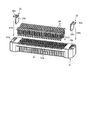
- FIG. 3 is an exploded perspective view showing an example of the connector according to the embodiment.
- FIG. 4 is a bottom view showing an example of the connector according to the embodiment.
- Drawing 5 is a figure showing an example of the 1st connector concerning an embodiment.
- Drawing 6 is a figure showing an example of the 2nd connector concerning an embodiment.
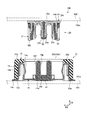
- FIG. 7 is a diagram showing a configuration along a cross section AA in FIG.
- FIG. 8 is a view showing a configuration along a cross section BB in FIG.
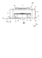
- FIG. 9 is a side view showing an example of the connector according to the embodiment.
- FIG. 1 is a perspective view showing an example of a connector according to the embodiment.
- FIG. 2 is a perspective view showing an example of a connector according to the embodiment.
- FIG. 3 is an exploded perspective view showing an example of the connector
- FIG. 10 is a diagram showing a flow of assembling the first connector according to the embodiment.
- Drawing 11 is a figure showing the flow which assembles the 2nd connector concerning an embodiment.
- Drawing 12 is a figure showing the state where the 1st connector concerning the embodiment and the 2nd connector were made to counter.
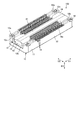
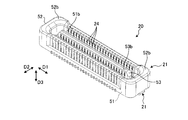
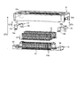
- FIGS. 1 and 2 are perspective views showing an example of a connector 100 according to the embodiment.
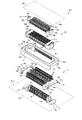
- FIG. 3 is an exploded perspective view showing the configuration of connector 100.
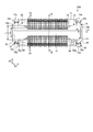
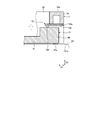
- FIG. 4 is a bottom view showing an example of the connector 100 as viewed from the first substrate 101 side.
- the connector 100 includes a first connector (connector) 10 and a second connector (other connector) 20. 1, 2 and 4 show a state in which the first connector 10 and the second connector 20 are fitted.
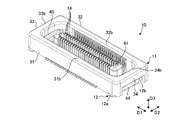
- FIG. 5 is a view showing an example of the first connector 10.
- FIG. 5 is a view showing an example of the first connector 10.
- FIG. 5 shows the first connector 10 as viewed from the side where the second connector 20 is fitted.
- FIG. 6 is a view showing an example of the second connector 20. As shown in FIG. FIG. 6 shows the second connector 20 as viewed from the side in which the first connector 10 is fitted.
- the first connector 10 is attached to the first substrate 101.
- the first connector 10 has a fixed insulator 11, a metal fitting 12, a movable insulator 13, and a contact 14.
- the fixed insulator 11 is formed in a rectangular frame shape using, for example, a resin material.
- the fixed insulator 11 is disposed at an interval from the substrate surface 101 a of the first substrate 101.
- the fixed insulator 11 has a wall 31 and a wall 32, and a beam 33 and a beam 34.
- the wall 31 and the wall 32 are disposed in parallel to the contact arrangement direction D1 of the fixed insulator 11.
- the contact arrangement direction D1 is a direction in which the plurality of contacts 14 are arranged in the first connector 10.
- the wall portion 31 is disposed on one side in the width direction D2 of the fixed insulator 11.
- the wall 32 is disposed on the other side in the width direction D2 of the fixed insulator 11.
- the width direction D2 is a direction perpendicular to the contact arranging direction D1 in a plane perpendicular to the fitting direction D3 in which the first connector 10 and the second connector 20 fit.
- the wall 31 has a fitting surface 31 b.
- the wall 32 has a fitting surface 32b.
- the fitting surface 31b and the fitting surface 32b are planes perpendicular to the fitting direction D3.
- the fitting surface 31 b and the fitting surface 32 b are flat.
- the fitting surface 31 b and the fitting surface 32 b slide the second connector 20 to guide the inside of the fixed insulator 11 when the second connector 20 is fitted to the first connector 10.
- the beam 33 and the beam 34 are parallel to the width direction D2.
- the beam portion 33 is disposed at one end of the contact arrangement direction D1.
- the beam portion 34 is disposed at the other end of the contact arrangement direction D1.
- the distance between the beam 33 and the substrate surface 101a and the distance between the beam 34 and the substrate surface 101a are larger than the distance between the wall 31 and the substrate surface 101a and the distance between the wall 32 and the substrate surface 101a.
- the beam portion 33 has a support surface 33 a facing the substrate surface 101 a.
- the beam portion 34 has a support surface 34 a facing the substrate surface 101 a.
- the support surface 33a and the support surface 34a are perpendicular to the fitting direction D3.
- the beam portion 33 has a fitting surface 33 b.
- the beam portion 34 has a fitting surface 34 b.
- the fitting surface 33 b and the fitting surface 34 b are planes parallel to the substrate surface 101 a.
- the fitting surface 33 b and the fitting surface 34 b are flat.
- the fitting surface 33 b and the fitting surface 34 b, and the fitting surface 31 b of the wall 31 and the fitting surface 32 b of the wall 32 are disposed on the same plane.
- the fitting surface 33 b and the fitting surface 34 b are continuously formed along the entire circumference of the fixed insulator 11 together with the fitting surface 31 b and the fitting surface 32 b.
- the fitting surface 33b and the fitting surface 34b, together with the fitting surface 31b and the fitting surface 32b slide the second connector 20 when the second connector 20 is fitted to the first connector 10, and the inner side of the fixed insulator 11 Guide to
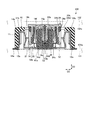
- the metal fitting 12 is provided inside the fixed insulator 11.
- the metal fitting 12 is locked in a state of being inserted into the fixed insulator 11 from the direction opposite to the direction in which the second connector 20 enters.
- the metal fitting 12 is arrange
- the fitting 12 is plate-shaped.
- the metal fitting 12 has a mounting portion 12a, an insulator support portion 12b, and an insulator locking portion 12c.
- the mounting portions 12 a are disposed at both ends of the metal fitting 12 and are bent toward the substrate surface 101 a.
- the mounting portion 12a is fixed to the substrate surface 101a.
- the insulator support 12b is parallel to a plane orthogonal to the fitting direction D3.
- the insulator support 12b is disposed in parallel to the width direction D2.
- the insulator support portion 12 b faces or abuts on the support surface 33 a and the support surface 34 a of the fixed insulator 11.
- the insulator locking portion 12 c is locked to the fixed insulator 11. As a result, the insulator support 12 b is located directly below the beam 33 and the beam 34.
- FIG. 7 is a diagram showing a configuration along a cross section AA in FIG.
- the insulator support 12 b has a protrusion 12 d.
- the convex portion 12 d protrudes from the insulator support portion 12 b to the movable insulator 13 side.
- the convex portion 12 d is formed, for example, in a hemispherical shape.
- FIG. 7 shows a configuration in which one convex portion 12 d is disposed, the present invention is not limited to this, and two or more convex portions 12 d may be provided.
- the movable insulator 13 is formed using, for example, a resin material.
- the movable insulator 13 is disposed inside the fixed insulator 11.
- the movable insulator 13 is disposed at an interval from the substrate surface 101a.
- the movable insulator 13 has a contact holding portion 41, an insertion hole 42, a locking portion 43 and a locking portion 44.
- the contact holding portion 41 extends in parallel to the contact arrangement direction D1.
- the contact holding unit 41 holds a plurality of contacts 14.
- the contact holding portion 41 has a groove 41 b (see FIG. 3) for holding the contact 14.
- the grooves 41 b are arranged at predetermined intervals in the contact arrangement direction D ⁇ b> 1 according to the number of the contacts 14.
- the contact holding portion 41 is disposed with respect to the wall portion 31 and the wall portion 32 of the fixed insulator 11 in a state of being spaced in the width direction D2. Further, the contact holding portion 41 is arranged in a state of being spaced from the beam 33 and the beam 34 of the fixed insulator 11 in the contact arrangement direction D1.
- FIG. 8 is a view showing a configuration along a cross section BB in FIG.
- the contact holding portion 41 has a bottom surface portion 41 a.
- the bottom surface portion 41 a faces the substrate surface 101 a of the first substrate 101.
- the bottom surface portion 41a is shaped so as to be apart from the virtual plane S from the center to both ends in the width direction D2.
- the virtual plane S is a plane facing the bottom surface portion 41a.
- the substrate surface 101 a is a virtual plane S.
- the shape of the bottom surface portion 41a may be a shape that is curved along the entire width direction D2, or a shape in which only both end sides in the width direction D2 are curved.
- the bottom surface portion 41a is curved, the bottom surface portion 41a and the substrate surface are movable even when the movable insulator 13 swings at an angle to the virtual plane S (substrate surface 101a) in the width direction D2. Contact with 101a is avoided. Therefore, for example, when the second connector 20 is fitted to the first connector 10 in a state where the second connector 20 is inclined with respect to the fitting direction D3, the fitting property is improved and also the first connector is fitted. 10 damage can be prevented.
- the insertion hole 42 is disposed at the center of the contact holding portion 41 as viewed from the fitting direction D3. A part of the second connector 20 is inserted into the insertion hole 42.
- the locking portion 43 is disposed at one end of the contact arranging direction D1 of the contact holding portion 41.
- the locking portion 44 is disposed at the other end of the contact arranging direction D1 of the contact holding portion 41.
- the locking portion 43 and the locking portion 44 are inserted between the insulator support portion 12 b of the metal fitting 12 and the substrate surface 101 a.
- the locking portion 43 and the locking portion 44 are disposed to face the convex portion 12 d of the insulator support portion 12 b. Movement of the movable insulator 13 in the fitting direction D3 is restricted by the locking portion 43 and the locking portion 44 disposed so as to face the convex portion 12d, that is, the movable insulator 13 does not come off with respect to the fixed insulator 11. To be held.
- the locking portion 43 and the locking portion 44 contact with each other locally at the convex portion 12 d instead of the entire insulator support portion 12 b, thereby reducing the sliding resistance.
- the width L1 of the locking portion 43 and the locking portion 44 which is the dimension in the width direction D2 (hereinafter, the dimension in the width direction D2 is referred to as the width), is larger than the width L2 of the contact holding portion 41 See Figure 4).
- the movable insulator 13 has the width L1 larger than the width L2, the strength of the locking portion 43 and the locking portion 44 is improved.
- FIG. 9 is a side view showing an example of the connector 100. As shown in FIG. FIG. 9 shows the case when viewed from the beam 34 side of the first connector 10. As shown in FIG. 9, the locking portion 44 has a bottom surface portion 44 a. The bottom surface portion 44 a faces the substrate surface 101 a of the first substrate 101. The bottom portion 44 a is shaped so as to be apart from the virtual plane S from the center to both ends in the width direction D2. The virtual plane S is a plane facing the bottom surface portion 44a. In the embodiment, for example, the substrate surface 101 a is set as the virtual plane S in the embodiment.
- the shape of the bottom portion 44a may be a shape that is curved in the entire width direction D2, or a shape in which only both end sides of the width direction D2 are curved.
- the bottom surface portion 44 a may be formed in the same plane as the bottom surface portion 41 a of the contact holding portion 41.
- the bottom surface 43 a (see FIG. 4) of the locking portion 43 also has the same configuration as the bottom surface 44 a of the locking portion 44. Since the bottom surface portion 43a and the bottom surface portion 44a have a curved shape, contact between the bottom surface portion 43a and the bottom surface portion 44a and the substrate surface 101a is avoided even when the movable insulator 13 swings in the width direction D2. .
- the first connector 10 allows the movable insulator 13 to swing in the width direction D2.
- the plurality of contacts 14 are arranged side by side in the contact arrangement direction D1.
- the contact 14 is formed, for example, by bending a metal member.
- the method of forming the contact 14 is not limited to bending, and may be formed, for example, by punching a metal member.
- the contact 14 includes a mounting portion 14a, a first locking portion 14b, an elastic deformation portion 14c, a second locking portion 14d, a third locking portion 14e, and a first connection portion. 14f and a second connection portion 14g.
- the mounting unit 14a is mounted on the substrate surface 101a.
- the first locking portion 14 b is locked to the fixed insulator 11.
- the elastically deformable portion 14c is provided between the first locking portion 14b and the second locking portion 14d, and is a portion that can be elastically deformed.
- the second locking portion 14 d and the third locking portion 14 e are locked to the contact holding portion 41 of the movable insulator 13.
- the first connection portion 14 f and the second connection portion 14 g contact the contacts 24 on the second connector 20 side.
- the first connection portion 14 f is disposed on the fixed insulator 11 side.
- the second connection portion 14 g is disposed inside the insertion hole 42.
- the second connector 20 is attached to the second substrate 102.
- the second connector 20 has an insulator 21, a fitting 22, and a contact 24.
- the insulator 21 is formed in a rectangular shape using, for example, a resin material.
- the insulator 21 is disposed at an interval from the substrate surface 102 a of the second substrate 102.
- the insulator 21 has a contact holding portion 51, an outer insertion portion 52, and an inner insertion portion 53.
- the contact holding portion 51 is disposed to face the substrate surface 102 a.
- the contact holding portion 51 extends in parallel to the contact arrangement direction D1.
- the contact holding unit 51 holds a plurality of contacts 24.
- the contact holding portion 51 has a groove 51 b (see FIG. 3) for holding the contact 24.
- the plurality of grooves 51 b are arranged at predetermined intervals in the contact arrangement direction D ⁇ b> 1 according to the number of the contacts 24.
- the distance between two adjacent groove portions 51b is the same as the distance between two adjacent groove portions 41b in the contact holding portion 41 on the first connector 10 side.
- the outer insertion portion 52 is provided integrally with the contact holding portion 51.
- the outer insertion portion 52 is formed in an annular shape (see FIG. 6).
- the outer insertion portion 52 includes the wall 31, the wall 32, the beam 33 and the beam 34 of the fixed insulator 11, and the contact holding portion 41 of the movable insulator 13. Placed between.
- the outer insertion portion 52 is disposed at a position surrounding the contact holding portion 41.
- the outer insertion portion 52 has a fitting surface 52b that faces the first connector 10 at the time of fitting (see FIG. 6).
- the inner insertion portion 53 is provided integrally with the contact holding portion 51.
- the inner insertion portion 53 is disposed inside the outer insertion portion 52 (see FIG. 6).
- the inner insertion portion 53 is formed in a plate shape.
- the inner insertion portion 53 is inserted into the insertion hole 42 of the movable insulator 13 when the second connector 20 is fitted to the first connector 10.
- the inner insertion portion 53 has a fitting surface 53 b facing the first connector 10 at the time of fitting (see FIG. 6).
- the fitting 22 is, for example, plate-like.
- the metal fitting 22 has a mounting portion 22a and an insulator locking portion 22b.
- the mounting portions 22 a are disposed at both ends of the insulator 21 and are disposed in parallel to the substrate surface 102 a.
- the mounting portion 22a is fixed to the substrate surface 102a.
- the insulator locking portion 22 b is bent to the inside of the insulator 21 with respect to the mounting portion 22 a.
- the insulator locking portion 22 b is locked to the insulator 21 in a state of being inserted into the metal fitting holding portion 21 b of the insulator 21.
- the plurality of contacts 24 are arranged side by side in the contact arrangement direction D1.
- the contact 24 is formed, for example, by punching a metal member.
- the method of forming the contacts 24 is not limited to punching, and may be formed by bending a metal member, for example.
- the contact 24 includes a mounting portion 24 a, a locking portion 24 b, a first connection portion 24 c, and a second connection portion 24 d.
- the mounting portion 24 a is mounted on the substrate surface 102 a.
- the locking portion 24 b is locked to the contact holding portion 51 of the insulator 21.
- the first connection portion 24 c is disposed on the inner peripheral surface of the outer insertion portion 52.
- the first connection portion 24 c is connected to a first connection portion 14 f of the contact 14 disposed in the first connector 10.
- the second connection portion 24 d is disposed on the outer peripheral surface of the inner insertion portion 53.
- the second connection portion 24 d is connected to a second connection portion 14 g of the contact 14 disposed in the first connector 10.
- FIG. 10 is a diagram showing a flow of assembling the first connector 10.
- the first assembly process (ST1 in FIG. 10) will be described.
- the plurality of contacts 14 are inserted into the groove 41 b of the movable insulator 13 from above.
- the plurality of contacts 14 are engaged with and held by the movable insulator 13.
- the second assembly process (ST2 in FIG. 10) will be described.
- the metal fitting 12 is inserted into the fixed insulator 11 from below.
- the insulator support portion 12 b abuts on the support surface 33 a and the support surface 34 a of the fixed insulator 11.
- the insulator locking portion 12 c is locked to the fixed insulator 11.
- the metal fitting 12 is locked to the fixed insulator 11 in a state where the metal fitting 12 is disposed inside the fixed insulator 11, that is, in a state where the metal fitting 12 is not exposed to the surface of the fixed insulator 11 on the fitting side.
- Either of the first assembly process and the second assembly process may be performed first.
- the third assembly process (ST3 in FIG. 10) will be described.
- the movable insulator 13 holding the plurality of contacts 14 is inserted from below into the fixed insulator 11 with the metal fitting 12 locked.
- the movable insulator 13 is disposed inside the fixed insulator 11 in a state where the locking portion 43 and the locking portion 44 of the movable insulator 13 face or abut on the metal fitting 12 respectively.
- the assembly of the first connector 10 is completed.
- FIG. 11 shows a flow of assembling the second connector 20.
- the fourth assembly process ST4 in FIG. 11
- the plurality of contacts 24 are inserted into the groove 51 b of the insulator 21 from above.
- the plurality of contacts 24 are engaged with the insulator 21 and held.
- the fifth assembly step (ST5 in FIG. 11) will be described.
- the metal fitting 22 is inserted into the metal fitting holding portion 21 b of the insulator 21 from above.
- the insulator locking portion 22b is locked to the insulator 21 inside the metal fitting holding portion 21b.
- the assembly of the second connector 20 is completed. Any of the fourth assembly process and the fifth assembly process may be performed first.
- FIG. 12 is a view showing a state in which the first connector 10 and the second connector 20 are opposed to each other.
- the fitting surface 31b, the fitting surface 32b, the fitting surface 33b, and the fitting surface 34b of the first connector 10 and the second The fitting surface 52 b and the fitting surface 53 b of the connector 20 are opposed to each other. From this state, the first connector 10 and the second connector 20 are moved relative to each other for alignment.
- the fixed insulator 11 of the first connector 10 and the insulator 21 of the second connector 20 are brought into contact with each other and slid in a direction perpendicular to the fitting direction D3.
- the fitting surface 31b, the fitting surface 32b, the fitting surface 33b, and the fitting surface 34b of the fixed insulator 11 are flat. Therefore, the second connector 20 smoothly moves along the fitting surface 31 b, the fitting surface 32 b, and the fitting surfaces 33 b and 34 b.
- the outer insertion portion 52 of the insulator 21 is inserted between the fixed insulator 11 on the first connector 10 side and the contact holding portion 41, and the inner insertion portion 53 is inserted into the insertion hole 42.
- the fixed insulator 11 and the movable insulator 13 and the insulator 21 are fitted.
- the first connection portion 24 c of the contact 24 contacts the first connection portion 14 f of the contact 14.
- the second connection portion 24 d of the contact 24 contacts the second connection portion 14 g of the contact 14.
- the contact 14 and the contact 24 are electrically connected.
- the movable insulator 13 Swings in the width direction D2. Therefore, for example, when the fixed insulator 11 and the movable insulator 13 of the first connector 10 and the insulator 21 of the second connector 20 are fitted in the state of being shifted in the width direction D2, the movable insulator 13 is in the width direction D2. By swinging, the positional relationship between the first connector 10 and the second connector 20 is easily restored.
- the bottom surface portion 41a, the bottom surface portion 43a, and the bottom surface portion 44a are curved, even if the movable insulator 13 swings in the width direction D2, the bottom surface portion 41a, the bottom surface portion 43a, and the bottom surface portion 44a Contact with the substrate surface 101a is avoided.
- the locking portion 43 and the locking portion 44 have a width L1 larger than the width L2 of the contact holding portion 41, and the strength is improved. Therefore, the locking portion 43 and the locking portion 44 are supported by the insulator support portion 12b of the fitting 12 without breakage.
- the metal fitting 12 is formed of metal and fixed to the substrate surface 101 a of the first substrate 101 by the mounting portion 12 a, it does not deform or move away from the substrate surface 101 a. The movement to the connector 20 side is surely restricted. Since direct application of force from the locking portion 43 and the locking portion 44 to the fixed insulator 11 is avoided, damage or the like of the fixed insulator 11 is suppressed.
- the outer insertion portion 52 of the insulator 21 is pulled out from between the fixed insulator 11 and the contact holding portion 41 and the inner insertion portion 53 is pulled out of the insertion hole 42 without damaging the fixed insulator 11 and the movable insulator 13. .
- the first connection portion 24c and the first connection portion 14f are separated, and the second connection portion 24d and the second connection portion 14g are separated.
- the electrical connection between the contact 14 and the contact 24 is broken.
- the locking portions 43 and the locking portions 44 at both ends of the movable insulator 13 in the contact arrangement direction D1 are disposed to face the metal fitting 12. Therefore, when the movable insulator 13 is pulled toward the second connector 20 when removing the second connector 20 from the first connector 10 or when an unintended force is applied, the metal insulator 12 of the movable insulator 13 is The movement in the fitting direction D3 (the direction in which the second connector 20 is removed) is restricted. As a result, direct application of force from the movable insulator 13 to the fixed insulator 11 is avoided, so that damage to the fixed insulator 11 can be suppressed at the time of removal or when an unintended force is applied.
- the metal fitting 12 is disposed inside the fixed insulator 11, that is, the metal fitting 12 is exposed to the fitting surface 31b, the fitting surface 32b, the fitting surface 33b, and the fitting surface 34b of the fixed insulator 11. It is latched by the fixed insulator 11 in the state which is not carried out. For this reason, as compared with the case where the metal fitting 12 is disposed on the surface of the fixed insulator 11, the scraping of the other connector by the metal fitting or the level difference on the surface of the fixed insulator 11 is reduced. As a result, when the first connector 10 and the second connector 20 are fitted, the second connector 20 can be slid more smoothly on the surface of the fixed insulator 11, so the second connector 20 can be moved to the first connector 10. It becomes easy to insert in As described above, the connector 100 can be reduced in size while suppressing the reduction in strength, and can further improve the fit when the first connector 10 and the second connector 20 are fitted.
- the width L1 of the locking portion 43 and the locking portion 44 is larger than the width L2 of the contact holding portion 41 in the movable insulator 13. For this reason, even in the case of reducing the width L2 of the contact holding portion 41 by downsizing, the strength reduction of the movable insulator 13 can be suppressed.
- the entire surfaces of the fitting surface 31 b, the fitting surface 32 b, the fitting surface 33 b, and the fitting surface 34 b are exposed to the second connector 20.
- the fitting surface 31b for guiding the second connector 20 the fitting surface 32b, the fitting surface 33b, and the fitting surface 34b are provided on the same plane on the fixed insulator 11, and It is flat.
- the fitting surface 31 b, the fitting surface 32 b, the fitting surface 33 b, and the fitting surface 34 b are continuously formed over the entire circumference of the fixed insulator 11 and are flat.
- the second connector 20 can be fitted with the fitting surface 31b, the fitting surface 32b, and the fitting surface 33b. And 34b can be moved smoothly, and can not be scraped with a metal fitting or the like. Therefore, since the second connector 20 can be guided easily and safely, the workability of the fitting operation is improved.
- the movable insulator 13 has a shape in which the bottom surface portion 41a and the bottom surface portion 44a opposed to the substrate surface 101a are separated from the substrate surface 101a from the center to both ends in the width direction D2. Thereby, even when the movable insulator 13 swings in the width direction D2, contact between the bottom surface 41a and the bottom surface 44a and the substrate surface 101a can be suppressed.
- the technical scope of the present invention is not limited to the above embodiment, and appropriate modifications can be made without departing from the scope of the present invention.
- the case where the protrusion 12d is provided on the insulator support 12b is described as an example. It is not limited to this.
- a convex portion may be provided on the locking portion 43 and the locking portion 44 side.
- the convex part may be provided in both the insulator support part 12b side, and the latching part 43 and the latching part 44 side.
- the shape of the bottom face part 41a of the movable insulator 13, the bottom face part 43a, and the bottom face part 44a mentioned the curved shape as an example was mentioned and demonstrated in the said embodiment, it does not limit to this.
- the shape of the movable insulator 13 is another shape as long as the bottom surface 41a, the bottom surface 43a and the bottom surface 44a do not contact the substrate surface 101a when the movable insulator 13 swings in the width direction D2. Good.
- the central portion in the width direction D2 has a planar shape parallel to the virtual plane S (substrate surface 101a), and a part of both end sides in the width direction D2 has a curved shape
- the bottom surface portion 41a, the bottom surface portion 43a, and the bottom surface portion 44a may have a planar shape (inclined surface) which is separated from the substrate surface 101a from the center to both ends in the width direction D2.
- the inclined surface may be disposed over the whole from the center to both ends in the width direction D2, or the central portion in the width direction D2 is a plane parallel to the virtual plane S (substrate surface 101a). Inclined surfaces may be disposed on part of both ends of the direction D2.
Landscapes
- Coupling Device And Connection With Printed Circuit (AREA)
- Details Of Connecting Devices For Male And Female Coupling (AREA)
Abstract
Description
D2 幅方向
D3 嵌合方向
L1 幅
L2 幅
S 仮想平面
10 第1コネクタ
11 固定インシュレータ
12,22 金具
12a,22a 実装部
12b インシュレータ支持部
12c,22b インシュレータ係止部
12d 凸部
13 可動インシュレータ
14,24 コンタクト
14a 実装部
14b 第1係止部
14c 弾性変形部
14d 第2係止部
14e 第3係止部
14f 第1接続部
14g 第2接続部
20 第2コネクタ
21 インシュレータ
24a 実装部
24b 係止部
24c 第1接続部
24d 第2接続部
31,32 壁部
31b,32b,33b,34b 嵌合面
33,34 梁部
33a,34a 支持面
41,51 コンタクト保持部
41a,43a,44a 底面部
42 挿入穴
43,44 係止部
52 外側挿入部
53 内側挿入部
52b,53b 嵌合面
100 コネクタ
101 第1基板
102 第2基板
101a,102a 基板面 D1 contact arrangement direction D2 width direction D3 fitting direction L1 width L2 width S
Claims (7)
- 他のコネクタと嵌合して、電気的に導通する複数のコンタクトを有するコネクタであって、
枠状である固定インシュレータと、
複数の前記コンタクトが配列される方向であるコンタクト配列方向について前記固定インシュレータの両端に配置され、前記固定インシュレータに内設された金具と、
前記固定インシュレータの内側に配置され、複数の前記コンタクトにより前記固定インシュレータと前記コンタクトの弾性変形部を介して連結され、前記弾性変形部の弾性変形により少なくとも前記他のコネクタと嵌合する嵌合方向に垂直な方向に可動可能であり、前記コンタクト配列方向の両端が前記金具に対向する可動インシュレータと、
を有する
コネクタ。 A connector having a plurality of contacts electrically connected by mating with another connector, the connector comprising:
A fixed insulator which is frame-shaped,
Metal fittings disposed at both ends of the fixed insulator in the contact arrangement direction, which is a direction in which the plurality of contacts are arranged, and provided in the fixed insulator.
A fitting direction disposed inside the fixed insulator, connected by the plurality of contacts via the elastically deformable portion of the fixed insulator and the contact, and engaged with at least the other connector by the elastic deformation of the elastically deformable portion A movable insulator movable in a direction perpendicular to the direction in which the both ends in the contact arrangement direction face the metal fitting;
With a connector. - 前記可動インシュレータは、前記コンタクト配列方向の中央部よりも前記両端の方が、前記嵌合方向に垂直な平面内で前記コンタクト配列方向に直交する幅方向に幅広く形成されている請求項1に記載のコネクタ。 2. The movable insulator according to claim 1, wherein the both ends of the movable insulator are formed wider in a width direction orthogonal to the contact arranging direction in a plane perpendicular to the fitting direction than a central portion in the contact arranging direction. Connector.
- 前記可動インシュレータの前記コンタクト配列方向の両端は、前記他のコネクタから抜去される際に、前記金具により規制がされる請求項1又は請求項2に記載のコネクタ。 The connector according to claim 1 or 2, wherein both ends of the movable insulator in the contact arrangement direction are restricted by the metal fitting when it is removed from the other connector.
- 前記固定インシュレータは、前記嵌合方向に前記固定インシュレータのみから形成される嵌合面を有している請求項1から請求項3のいずれか一項に記載のコネクタ。 The connector according to any one of claims 1 to 3, wherein the fixed insulator has a fitting surface formed of only the fixed insulator in the fitting direction.
- 前記嵌合面は、同一平面上に設けられ、かつ平坦である請求項4に記載のコネクタ。 The connector according to claim 4, wherein the fitting surface is provided on the same plane and is flat.
- 前記嵌合面は、前記固定インシュレータの全周に亘って連続して形成され、かつ平坦である請求項4又は請求項5に記載のコネクタ。 The connector according to claim 4 or 5, wherein the fitting surface is continuously formed over the entire circumference of the fixed insulator and flat.
- 前記可動インシュレータは、前記他のコネクタと嵌合する面とは反対側の底面が、前記嵌合方向に垂直な方向の中央から端部に至るにつれて、前記底面に対向する仮想平面から離れる形状である請求項1から請求項6のいずれか一項に記載のコネクタ。 The movable insulator has a shape in which a bottom surface opposite to a surface to be fitted with the other connector is separated from a virtual plane opposed to the bottom surface as it extends from the center to the end in a direction perpendicular to the fitting direction. The connector according to any one of claims 1 to 6.
Priority Applications (5)
| Application Number | Priority Date | Filing Date | Title |
|---|---|---|---|
| JP2018502029A JP6371491B2 (en) | 2016-08-10 | 2017-08-10 | connector |
| US16/324,085 US10833443B2 (en) | 2016-08-10 | 2017-08-10 | Connector |
| EP17839586.9A EP3499651A4 (en) | 2016-08-10 | 2017-08-10 | Connector |
| CN201780048679.3A CN109565123B (en) | 2016-08-10 | 2017-08-10 | Connector with a locking member |
| KR1020197003731A KR102202564B1 (en) | 2016-08-10 | 2017-08-10 | connector |
Applications Claiming Priority (2)
| Application Number | Priority Date | Filing Date | Title |
|---|---|---|---|
| JP2016-158225 | 2016-08-10 | ||
| JP2016158225 | 2016-08-10 |
Publications (1)
| Publication Number | Publication Date |
|---|---|
| WO2018030522A1 true WO2018030522A1 (en) | 2018-02-15 |
Family
ID=61163105
Family Applications (1)
| Application Number | Title | Priority Date | Filing Date |
|---|---|---|---|
| PCT/JP2017/029147 WO2018030522A1 (en) | 2016-08-10 | 2017-08-10 | Connector |
Country Status (6)
| Country | Link |
|---|---|
| US (1) | US10833443B2 (en) |
| EP (1) | EP3499651A4 (en) |
| JP (4) | JP6371491B2 (en) |
| KR (1) | KR102202564B1 (en) |
| CN (1) | CN109565123B (en) |
| WO (1) | WO2018030522A1 (en) |
Cited By (1)
| Publication number | Priority date | Publication date | Assignee | Title |
|---|---|---|---|---|
| JP2018037150A (en) * | 2016-08-29 | 2018-03-08 | ヒロセ電機株式会社 | Electrical connector for circuit board |
Families Citing this family (7)
| Publication number | Priority date | Publication date | Assignee | Title |
|---|---|---|---|---|
| JP7196468B2 (en) | 2018-08-29 | 2022-12-27 | 大同特殊鋼株式会社 | RTB system sintered magnet |
| TWI711232B (en) * | 2019-06-17 | 2020-11-21 | 唐虞企業股份有限公司 | Electrical connector |
| JP6687790B1 (en) * | 2019-07-26 | 2020-04-28 | 京セラ株式会社 | Connector and electronic equipment |
| JP7303942B2 (en) | 2020-04-30 | 2023-07-05 | 本田技研工業株式会社 | swing arm structure |
| JP1719731S (en) * | 2021-09-30 | 2022-07-13 | electrical connector | |
| JP1719683S (en) * | 2021-09-30 | 2022-07-13 | electrical connector | |
| JP1719682S (en) * | 2021-09-30 | 2022-07-13 | electrical connector |
Citations (4)
| Publication number | Priority date | Publication date | Assignee | Title |
|---|---|---|---|---|
| JP3007812U (en) * | 1994-05-25 | 1995-02-28 | モレックス インコーポレーテッド | Surface mount electrical connector |
| JP2004063358A (en) * | 2002-07-31 | 2004-02-26 | Hirose Electric Co Ltd | Floating electric connector |
| JP2004227911A (en) * | 2003-01-22 | 2004-08-12 | Smk Corp | Floating connector |
| JP2014067706A (en) | 2012-09-05 | 2014-04-17 | Iriso Electronics Co Ltd | Connector |
Family Cites Families (23)
| Publication number | Priority date | Publication date | Assignee | Title |
|---|---|---|---|---|
| JP2568142B2 (en) | 1991-12-30 | 1996-12-25 | モレックス インコーポレーテッド | Floating structure electrical connector and manufacturing method thereof |
| JPH06163125A (en) | 1992-11-25 | 1994-06-10 | Matsushita Electric Works Ltd | Connector between substrates |
| JP3007812B2 (en) | 1995-05-19 | 2000-02-07 | シャープ株式会社 | Liquid crystal display device and method of manufacturing the same |
| JPH09320708A (en) | 1996-05-31 | 1997-12-12 | Matsushita Electric Works Ltd | Floating connector |
| JPH10312868A (en) * | 1997-05-13 | 1998-11-24 | Sumitomo Wiring Syst Ltd | Board connector |
| JPH10326651A (en) | 1997-05-27 | 1998-12-08 | Sumitomo Wiring Syst Ltd | Connector for board |
| US8014974B2 (en) * | 2001-12-19 | 2011-09-06 | Caterpillar Inc. | System and method for analyzing and reporting machine operating parameters |
| JP3929946B2 (en) | 2003-07-29 | 2007-06-13 | 矢崎総業株式会社 | connector |
| JP4287825B2 (en) * | 2005-01-28 | 2009-07-01 | モレックス インコーポレイテド | Board connector |
| JP2006216298A (en) | 2005-02-02 | 2006-08-17 | Honda Tsushin Kogyo Co Ltd | Floating type electric connector |
| JP2007018785A (en) * | 2005-07-06 | 2007-01-25 | D D K Ltd | Connector |
| JP4969838B2 (en) * | 2005-11-28 | 2012-07-04 | モレックス インコーポレイテド | Floating type connector |
| JP2007220327A (en) * | 2006-02-14 | 2007-08-30 | Kel Corp | Floating type connector |
| JP5166931B2 (en) | 2008-03-21 | 2013-03-21 | 第一電子工業株式会社 | Electrical connector |
| JP5000560B2 (en) | 2008-03-21 | 2012-08-15 | 第一電子工業株式会社 | Electrical connector |
| JP5185731B2 (en) * | 2008-08-27 | 2013-04-17 | 第一電子工業株式会社 | Floating connector fixture and floating connector using the fixture |
| JP4374074B1 (en) * | 2009-06-10 | 2009-12-02 | イリソ電子工業株式会社 | Electrical connection terminal and connector using the same |
| JP2011249076A (en) * | 2010-05-25 | 2011-12-08 | Fujitsu Component Ltd | Floating connector |
| JP5590991B2 (en) * | 2010-06-30 | 2014-09-17 | 京セラコネクタプロダクツ株式会社 | connector |
| JP5499191B1 (en) * | 2013-01-28 | 2014-05-21 | 日本航空電子工業株式会社 | connector |
| JP5946804B2 (en) * | 2013-08-09 | 2016-07-06 | ヒロセ電機株式会社 | connector |
| US9391398B2 (en) * | 2014-03-20 | 2016-07-12 | Japan Aviation Electronics Industry, Limited | Connector assembly |
| JP6771989B2 (en) * | 2016-08-09 | 2020-10-21 | ヒロセ電機株式会社 | Electrical connector for circuit board |
-
2017
- 2017-08-10 EP EP17839586.9A patent/EP3499651A4/en active Pending
- 2017-08-10 KR KR1020197003731A patent/KR102202564B1/en active IP Right Grant
- 2017-08-10 US US16/324,085 patent/US10833443B2/en active Active
- 2017-08-10 JP JP2018502029A patent/JP6371491B2/en active Active
- 2017-08-10 CN CN201780048679.3A patent/CN109565123B/en active Active
- 2017-08-10 WO PCT/JP2017/029147 patent/WO2018030522A1/en unknown
-
2018
- 2018-07-12 JP JP2018132450A patent/JP2018160471A/en active Pending
- 2018-07-12 JP JP2018132591A patent/JP6656317B2/en active Active
-
2019
- 2019-06-25 JP JP2019117547A patent/JP2019186219A/en active Pending
Patent Citations (4)
| Publication number | Priority date | Publication date | Assignee | Title |
|---|---|---|---|---|
| JP3007812U (en) * | 1994-05-25 | 1995-02-28 | モレックス インコーポレーテッド | Surface mount electrical connector |
| JP2004063358A (en) * | 2002-07-31 | 2004-02-26 | Hirose Electric Co Ltd | Floating electric connector |
| JP2004227911A (en) * | 2003-01-22 | 2004-08-12 | Smk Corp | Floating connector |
| JP2014067706A (en) | 2012-09-05 | 2014-04-17 | Iriso Electronics Co Ltd | Connector |
Non-Patent Citations (1)
| Title |
|---|
| See also references of EP3499651A4 |
Cited By (1)
| Publication number | Priority date | Publication date | Assignee | Title |
|---|---|---|---|---|
| JP2018037150A (en) * | 2016-08-29 | 2018-03-08 | ヒロセ電機株式会社 | Electrical connector for circuit board |
Also Published As
| Publication number | Publication date |
|---|---|
| CN109565123B (en) | 2020-12-22 |
| US10833443B2 (en) | 2020-11-10 |
| JP2018160471A (en) | 2018-10-11 |
| KR20190026011A (en) | 2019-03-12 |
| KR102202564B1 (en) | 2021-01-13 |
| JP6371491B2 (en) | 2018-08-08 |
| EP3499651A4 (en) | 2020-04-08 |
| CN109565123A (en) | 2019-04-02 |
| JPWO2018030522A1 (en) | 2018-08-09 |
| JP2019186219A (en) | 2019-10-24 |
| JP2018160472A (en) | 2018-10-11 |
| JP6656317B2 (en) | 2020-03-04 |
| US20190214762A1 (en) | 2019-07-11 |
| EP3499651A1 (en) | 2019-06-19 |
Similar Documents
| Publication | Publication Date | Title |
|---|---|---|
| WO2018030522A1 (en) | Connector | |
| WO2017115693A1 (en) | Floating connector device | |
| US7798871B2 (en) | Contact and electrical connector having increased connection object removal force | |
| WO2015186493A1 (en) | Connector | |
| JP5615157B2 (en) | Connector and contact used for it | |
| KR200496585Y1 (en) | Floating connector | |
| EP3346556A1 (en) | Electrical interface | |
| TW201320492A (en) | Connector capable of reducing occurrence of a contact failure | |
| WO2015063817A1 (en) | Socket, connector using such socket, and header used in such connector | |
| WO2020085036A1 (en) | Connector and method of manufacturing same | |
| JP6766151B2 (en) | connector | |
| JP7247621B2 (en) | female contact | |
| JP2013055007A (en) | Connector | |
| WO2015063818A1 (en) | Socket, connector provided with such socket, and header used in such connector | |
| US20160036149A1 (en) | Connector | |
| JP5995196B2 (en) | Electrical junction box | |
| CN111755862A (en) | Floating connector | |
| JP3230169U (en) | Floating connector | |
| JP6452531B2 (en) | connector | |
| KR200495150Y1 (en) | Floating busbar connection assembly | |
| CN113661614A (en) | Connector, connecting device and connecting method | |
| US20170338583A1 (en) | Electrical Connector Allowing Disassembly, Electronic Module, and Assembly Method | |
| JP5763447B2 (en) | connector | |
| CN115241671A (en) | Polygonal connector | |
| CN112928549A (en) | Connector housing |
Legal Events
| Date | Code | Title | Description |
|---|---|---|---|
| ENP | Entry into the national phase |
Ref document number: 2018502029 Country of ref document: JP Kind code of ref document: A |
|
| 121 | Ep: the epo has been informed by wipo that ep was designated in this application |
Ref document number: 17839586 Country of ref document: EP Kind code of ref document: A1 |
|
| ENP | Entry into the national phase |
Ref document number: 20197003731 Country of ref document: KR Kind code of ref document: A |
|
| NENP | Non-entry into the national phase |
Ref country code: DE |
|
| ENP | Entry into the national phase |
Ref document number: 2017839586 Country of ref document: EP Effective date: 20190311 |