WO2017133105A1 - Electrochromic structure and method of forming same - Google Patents
Electrochromic structure and method of forming same Download PDFInfo
- Publication number
- WO2017133105A1 WO2017133105A1 PCT/CN2016/081232 CN2016081232W WO2017133105A1 WO 2017133105 A1 WO2017133105 A1 WO 2017133105A1 CN 2016081232 W CN2016081232 W CN 2016081232W WO 2017133105 A1 WO2017133105 A1 WO 2017133105A1
- Authority
- WO
- WIPO (PCT)
- Prior art keywords
- conductive layer
- layer
- isolation region
- conductive
- light shielding
- Prior art date
Links
Images


Classifications
-
- G—PHYSICS
- G02—OPTICS
- G02F—OPTICAL DEVICES OR ARRANGEMENTS FOR THE CONTROL OF LIGHT BY MODIFICATION OF THE OPTICAL PROPERTIES OF THE MEDIA OF THE ELEMENTS INVOLVED THEREIN; NON-LINEAR OPTICS; FREQUENCY-CHANGING OF LIGHT; OPTICAL LOGIC ELEMENTS; OPTICAL ANALOGUE/DIGITAL CONVERTERS
- G02F1/00—Devices or arrangements for the control of the intensity, colour, phase, polarisation or direction of light arriving from an independent light source, e.g. switching, gating or modulating; Non-linear optics
- G02F1/01—Devices or arrangements for the control of the intensity, colour, phase, polarisation or direction of light arriving from an independent light source, e.g. switching, gating or modulating; Non-linear optics for the control of the intensity, phase, polarisation or colour
- G02F1/15—Devices or arrangements for the control of the intensity, colour, phase, polarisation or direction of light arriving from an independent light source, e.g. switching, gating or modulating; Non-linear optics for the control of the intensity, phase, polarisation or colour based on an electrochromic effect
- G02F1/153—Constructional details
- G02F1/1533—Constructional details structural features not otherwise provided for
-
- G—PHYSICS
- G02—OPTICS
- G02F—OPTICAL DEVICES OR ARRANGEMENTS FOR THE CONTROL OF LIGHT BY MODIFICATION OF THE OPTICAL PROPERTIES OF THE MEDIA OF THE ELEMENTS INVOLVED THEREIN; NON-LINEAR OPTICS; FREQUENCY-CHANGING OF LIGHT; OPTICAL LOGIC ELEMENTS; OPTICAL ANALOGUE/DIGITAL CONVERTERS
- G02F1/00—Devices or arrangements for the control of the intensity, colour, phase, polarisation or direction of light arriving from an independent light source, e.g. switching, gating or modulating; Non-linear optics
- G02F1/01—Devices or arrangements for the control of the intensity, colour, phase, polarisation or direction of light arriving from an independent light source, e.g. switching, gating or modulating; Non-linear optics for the control of the intensity, phase, polarisation or colour
- G02F1/15—Devices or arrangements for the control of the intensity, colour, phase, polarisation or direction of light arriving from an independent light source, e.g. switching, gating or modulating; Non-linear optics for the control of the intensity, phase, polarisation or colour based on an electrochromic effect
- G02F1/1514—Devices or arrangements for the control of the intensity, colour, phase, polarisation or direction of light arriving from an independent light source, e.g. switching, gating or modulating; Non-linear optics for the control of the intensity, phase, polarisation or colour based on an electrochromic effect characterised by the electrochromic material, e.g. by the electrodeposited material
- G02F1/1523—Devices or arrangements for the control of the intensity, colour, phase, polarisation or direction of light arriving from an independent light source, e.g. switching, gating or modulating; Non-linear optics for the control of the intensity, phase, polarisation or colour based on an electrochromic effect characterised by the electrochromic material, e.g. by the electrodeposited material comprising inorganic material
- G02F1/1525—Devices or arrangements for the control of the intensity, colour, phase, polarisation or direction of light arriving from an independent light source, e.g. switching, gating or modulating; Non-linear optics for the control of the intensity, phase, polarisation or colour based on an electrochromic effect characterised by the electrochromic material, e.g. by the electrodeposited material comprising inorganic material characterised by a particular ion transporting layer, e.g. electrolyte
-
- G—PHYSICS
- G02—OPTICS
- G02F—OPTICAL DEVICES OR ARRANGEMENTS FOR THE CONTROL OF LIGHT BY MODIFICATION OF THE OPTICAL PROPERTIES OF THE MEDIA OF THE ELEMENTS INVOLVED THEREIN; NON-LINEAR OPTICS; FREQUENCY-CHANGING OF LIGHT; OPTICAL LOGIC ELEMENTS; OPTICAL ANALOGUE/DIGITAL CONVERTERS
- G02F1/00—Devices or arrangements for the control of the intensity, colour, phase, polarisation or direction of light arriving from an independent light source, e.g. switching, gating or modulating; Non-linear optics
- G02F1/01—Devices or arrangements for the control of the intensity, colour, phase, polarisation or direction of light arriving from an independent light source, e.g. switching, gating or modulating; Non-linear optics for the control of the intensity, phase, polarisation or colour
- G02F1/15—Devices or arrangements for the control of the intensity, colour, phase, polarisation or direction of light arriving from an independent light source, e.g. switching, gating or modulating; Non-linear optics for the control of the intensity, phase, polarisation or colour based on an electrochromic effect
- G02F1/153—Constructional details
- G02F1/155—Electrodes
Definitions
- the present invention relates to the field of glass technology, and in particular to an electrochromic structure and a method of forming the same.
- Electrochromism means that the properties of the material such as reflectance, transmittance, and absorptivity can be reversibly changed according to the magnitude and polarity of the electric field under the action of an applied electric field.
- the electrochromic structure is formed on the surface of the glass to form an electrochromic glass, and the control of the light transmission property of the glass can be realized by voltage control.
- the energy consumption of buildings accounts for nearly 40% of the total energy consumption: the loss of heat from windows with poor isolation performance accounts for 10% to 30% of the heat loss in the winter of the building; Light inside the building increases the amount of energy needed for indoor cooling. It is estimated that the annual energy loss in the United States due to building glazing is about $20 billion.
- the electrochromic glass can control the amount of light transmitted by the glass and the amount of glare, and can optimize the amount of light transmitted through the glass and the amount of heat transmitted through the glass to maintain comfortable indoor conditions, thereby reducing energy consumption for maintaining the temperature of the building room. Therefore, with the rapid development of material technology, electrochromic glass has gradually been applied to automotive anti-glare mirrors, automotive sunroofs, high-speed rail windows, aircraft windows, curtain wall glass of high-end buildings. Moreover, with the gradual reduction of the comprehensive use cost, electrochromic glass can gradually replace Low-e glass, and is widely used in energy-saving and environmentally-friendly intelligent buildings.
- the problem addressed by the present invention is to provide an electrochromic structure and a method of forming the same to improve the performance of electrochromic glass.
- an electrochromic structure comprising:
- a substrate comprising a first side and a second side opposite the first side;
- a second conductive layer on the surface of the color changing functional layer, the second conductive layer being separated into a first isolation region and a first conductive region electrically isolated from each other;
- a first electrode located in the first isolation region of the second conductive layer, and electrically connected to the first conductive layer through the electrochromic layer;
- a second electrode located on a surface of the first conductive region of the second conductive layer, electrically connected to the second conductive layer of the first conductive region;
- the first light shielding layer is configured to block the first isolation area.
- the first light shielding layer covers the first electrode and the second conductive layer of the first isolation region.
- the first light shielding layer covers a portion of the second surface of the substrate corresponding to the first isolation region.
- a projected area of the first light shielding layer on the surface of the substrate is larger than a projected area of the first isolation area on the surface of the substrate.
- the electrochromic structure further includes: a first trench penetrating the second conductive layer, the first trench dividing the second conductive layer into a first isolation region and a first conductive region ;
- the first light shielding layer also blocks the first trench.
- the first light shielding layer covers the first electrode and the second conductive layer of the first isolation region, and fills the first trench.
- the first light shielding layer covers a portion of the second surface of the substrate corresponding to the first isolation region and the first trench.
- the material of the first light shielding layer comprises a metal.
- the first conductive layer includes a second isolation region and a second conduction region electrically isolated from each other;
- the electrochromic structure further includes: a second light shielding layer for shielding the second isolation region.
- a position of the second electrode corresponds to a position of the second isolation region
- the second light shielding layer covers the second electrode
- a second conductive layer covering the first conductive region a portion corresponding to the second isolation region
- the second light shielding layer covers a portion of the second surface of the substrate corresponding to the second isolation region.
- a projected area of the second light shielding layer on the surface of the substrate is larger than a projected area of the second isolation area on the surface of the substrate.
- the electrochromic structure further includes: a second trench penetrating the first conductive layer, the second trench dividing the first conductive layer into a second isolation region and a second conduction region ;
- the second light shielding layer also blocks the second trench.
- a position of the second electrode corresponds to a position of the second isolation region
- the second light shielding layer covers the second electrode
- a second conductive layer covering the first conductive region a portion corresponding to the second isolation region and the second trench.
- the second light shielding layer covers a portion of the second surface of the substrate corresponding to the second isolation region and the second trench.
- the first isolation region and the second isolation region have a width ranging from 1 micrometer to 500 micrometers, and the first conductive region and the second conductive region have a width ranging from 1 cm to 500 cm.
- the substrate comprises a light transmissive substrate.
- the electrochromic structure further comprises a barrier layer between the substrate and the first conductive layer.
- the material of the first conductive layer and the second conductive layer comprises a transparent conductive oxide.
- the present invention also provides a method for forming an electrochromic structure, comprising:
- the substrate comprising a first face and a second face opposite the first face;
- the second conductive layer Forming a second conductive layer on a surface of the color changing functional layer, the second conductive layer including a first isolation region and a first conductive region electrically isolated from each other;
- the first light shielding layer covers the first electrode and the second conductive layer of the first isolation region.
- the first light shielding layer is formed on a second surface of the substrate at a position corresponding to the first isolation region.
- a projected area of the first light shielding layer on the surface of the substrate is larger than a projected area of the first isolation area on the surface of the substrate.
- the forming method further includes: after forming the second conductive layer, forming a first trench penetrating the second conductive layer before forming the first electrode, the first trench
- the second conductive layer is divided into a first isolation region and a first conduction region;
- the first light shielding layer also blocks the first trench.
- the first light shielding layer covers the first electrode and the second conductive layer of the first isolation region, and fills the first trench.
- the method further includes: forming the first light shielding layer at a portion of the second surface of the substrate corresponding to the first isolation region and the first trench.
- the first conductive layer includes a second isolation region and a second conduction region electrically isolated from each other;
- the forming method further includes forming a second light shielding layer that blocks the second isolation region.
- a position of the second electrode corresponds to a position of the second isolation region
- the second light shielding layer covers the second electrode
- a second conductive layer covering the first conductive region a portion corresponding to the second isolation region
- the second light shielding layer is formed on a portion of the second surface of the substrate corresponding to the second isolation region.
- a projected area of the second light shielding layer on the surface of the substrate is larger than a projected area of the second isolation area on the surface of the substrate.
- the forming method further includes: after forming the first conductive layer, after forming the color changing functional layer, forming a second trench penetrating the first conductive layer, the second trench a conductive layer is divided into a second isolation region and a second conduction region;
- the second light shielding layer also blocks the second trench.
- a position of the second electrode corresponds to a position of the second isolation region
- the second light shielding layer covers the second electrode
- a second conductive layer covering the first conductive region a portion corresponding to the second isolation region and the second trench.
- the second light shielding layer is formed on a second surface of the substrate at a position corresponding to the second isolation region and the second trench.
- the first light shielding layer or the second light shielding layer is formed by screen printing, vacuum thermal evaporation coating, vacuum magnetron sputtering coating, vacuum ion source plating, and inkjet printing.
- the invention provides a first light shielding layer for shielding light to block the first isolation region, and can block the light leakage of the first isolation region after the electrochromic glass is discolored, thereby facilitating the improvement of the color uniformity of the electrochromic glass. To improve the performance of electrochromic glass.
- the first conductive layer further includes a second isolation region and a second conductive region electrically isolated from each other, and thus the electrochromic glass further includes a second light shielding that blocks the second isolation region
- the layer in order to block the light leakage of the second isolation region, is beneficial to improve the discoloration uniformity of the electrochromic glass, thereby improving the performance of electrochromism.
- a projected area of the first light shielding layer and the second light shielding layer on the surface of the substrate is greater than a projection of the first isolation region and the second isolation region on the surface of the substrate, respectively.
- the area can reduce light leakage caused by light diffraction, and further improve the shading performance of the electrochromic glass.
- FIG. 1 is a schematic cross-sectional structural view of an electrochromic structure
- FIG. 2 is a schematic flow chart of an embodiment of a method for forming an electrochromic structure of the present invention
- FIG. 15 are schematic structural views showing the intermediate structure of each step of an embodiment of the method for forming an electrochromic structure according to the present invention.
- Figure 16 is a cross-sectional structural view showing another embodiment of the method for forming an electrochromic structure of the present invention.
- the electrochromic glass comprises a substrate 10 and a first conductive layer 11, an electrochromic layer 12 and a second conductive layer 13 which are sequentially located on the surface of the substrate 10; the second conductive layer 13 and the electrophoresis are sequentially penetrated.
- the first electrode 14a of the color changing layer 12 and the second electrode 14b located on the surface of the second conductive layer 13 are electrically connected to the first conductive layer 11 and the second conductive layer 13, respectively, to the first conductive layer 11 and the second conductive layer
- the voltage signal is applied to form an electric field between the first conductive layer 11 and the second conductive layer 13 to control the color of the electrochromic layer 12.
- the second conductive layer 13 is divided into a first isolation region 13i and a first conduction region 13t that are electrically isolated from each other, and the first electrode 14a is located at the first In the isolation region 13i, the second electrode 14b is located in the first conduction region 13t.
- the potential between the second conductive layer 13 of the first isolation region 13i and the corresponding region of the first conductive layer 11 is equal, and an electric field cannot be formed, so when the color is discolored,
- the electrochromic layer 12 between the second conductive layer 13 of the first isolation region 13i and the corresponding region of the first conductive layer 11 does not change color, so that light leakage occurs.
- FIG. 2 is a schematic flow chart of an embodiment of a method for forming an electrochromic structure of the present invention.
- FIG. 3 to FIG. 15 are schematic structural views showing the intermediate structure of each step of an embodiment of the method for forming an electrochromic structure according to the present invention.
- a substrate 100 is provided, the substrate 100 including a first side and a second side opposite the first side.
- the substrate is used to provide a physical support platform.
- the substrate 100 can be a flexible substrate or a rigid substrate.
- the substrate 100 may be a light transmissive material.
- the substrate 100 is glass.
- the electrochromic glass can be formed by directly pressing the glass on the formed electrochromic structure, which can simplify the structure of the electrochromic glass and reduce the weight of the electrochromic glass.
- the number of electrochromic structures is not limited.
- the electrochromic structure can be sandwiched between two glasses to form an electrochromic structure, thereby reducing the requirements on the process machine. Reduce manufacturing costs.
- a first conductive layer 110 is formed on the first side of the substrate 100.
- the first conductive layer 110 is formed on a first side of the substrate 100, and the first conductive layer 110 is used to apply a voltage to form an electric field.
- the material of the first conductive layer 110 includes Transparent Conductive Oxide (TCO).
- TCO Transparent Conductive Oxide
- the first conductive layer 110 may be indium tin oxide (ITO), zinc tin oxide (IZO), zinc aluminum oxide (AZO), fluorine doped tin oxide (FTO), gallium doped tin oxide (GTO), etc.
- One or more of the materials; or a conductive transparent nitride including one or more of titanium nitride, titanium oxynitride, tantalum nitride, and yttrium oxynitride; or transparent conductive Graphene material; may also be other transparent metal or alloy materials.
- the thickness of the first conductive layer 110 ranges from 10 nanometers to 1000 nanometers.
- the first conductive layer 110 has a thickness ranging from 100 nanometers to 600 nanometers.
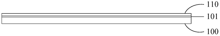
- the electrochromic structure is further The barrier layer 101 is disposed between the substrate 100 and the first conductive layer 110, so the forming method may further include forming a barrier layer 101 covering the surface of the substrate 100 before forming the first conductive layer 110.
- the substrate 100 is soda glass
- the barrier layer 101 is two in order to prevent the sodium ions in the soda glass from diffusing into the first conductive layer 110 to lower the electrical conductivity of the first conductive layer 110.
- a color-changing functional layer 120 on the surface of the first conductive layer 110 is formed.
- the first conductive layer 110 includes a second isolation region electrically isolated from each other. And a second conductive region, the number of the second isolation regions is one or more, and the number of the second conductive regions is one or more.
- the second isolation region and the second conductive region are separated by a second trench. Therefore, referring to step S210 in FIG. 2, after forming the first conductive layer, forming a second trench penetrating the first conductive layer, the second trench dividing the first conductive layer into the second isolation region and the second conductive region .
- FIG. 4 is a top plan view showing the intermediate structure of the electrochromic structure
- FIG. 5 is a cross-sectional view taken along line AA of FIG.
- the forming method further includes: forming a lower trench 111 penetrating the first conductive layer 110, the lower trench 111 dividing the first conductive layer 110 into a lower isolation region 110i and lower conduction zone 110t.
- the lower trench 111 constitutes the second trench
- the lower isolation region 110i constitutes the second isolation region
- the lower conductive region 110t constitutes the second conductive region.
- the lower isolation region 110i has a width ranging from 1 micrometer to 500 micrometers, and the lower conductive region 110t has a width ranging from 1 centimeters to 500 centimeters.
- the width range of the lower isolation region 110i has a width ranging from 5 cm to 50 cm.
- the lower trench 111 may extend along a "several" shape, and the plurality of lower isolation regions 110i thus formed communicate with each other to form a comb shape, and the plurality of lower conductive regions 110t communicate with each other to form a comb shape.
- the comb formed by the region 110t and the comb-like comb teeth formed by the plurality of lower isolation regions 110i compensate each other.
- the lower isolation region 110i has a width (comb width) ranging from 5 cm to 50 cm, a lower conduction region 110t between adjacent comb teeth, and a lower conduction region 110t having a width ranging from 5 cm to 50 cm.
- the width of the lower trench 111 ranges from 1 micrometer to 50 micrometers.
- the lower trench 111 has a width ranging from 2 micrometers to 10 micrometers to improve insulation between the lower isolation region 110i and the lower conductive region 110t.
- the lower trench 111 may be formed in the first conductive layer 110 by laser scribing.
- the lower trench 111 may be formed by a visible light laser scribing process or an infrared laser scribing process.
- a constant power output or a pulse power output can be used in the laser scribing process.
- the lower trench 111 is formed by pulse laser scribing, the pulse frequency ranges from 5 kHz to 500 kHz, and the laser power ranges from 0.1 watt to 10 watts. In some embodiments, the laser power ranges from 0.5 watts to 5 watts. It should be noted that the method of forming the lower trench 111 by laser scribing is only an example, and the specific method for forming the lower trench 111 is not limited in the present invention.
- the forming method further includes: clearing Dust residue to obtain a clean process surface.
- step S300 in FIG. 2, and in conjunction with FIG. 6, forms a color-changing functional layer 120 on the surface of the first conductive layer 110.
- the forming method further comprises: removing dust residue to remove the formation
- the residual dust generated during the trench 111 is described to provide a clean surface for subsequent processing steps.
- the color changing functional layer 120 is used to change color under voltage control.
- the color changing functional layer 120 includes one or more functional layers, and the step of forming the color changing functional layer 120 includes: forming one or more functional layers including an electrochromic layer, an ion storage layer, and an electrolysis An ion conducting layer between the color changing layer and the ion storage layer.
- the electrochromic layer is used for redox reaction under the action of an external electric field, and the color changes, and may be a cathodic electrochromic metal oxide, that is, a metal oxide whose color changes after ion implantation, such as under-oxidation.
- tungsten WO x, 2.7 ⁇ x ⁇ 3
- titanium oxide TiO 2
- vanadium oxide V 2 O 5
- niobium oxide Nb 2 O 5
- MoO 3 molybdenum oxide
- tantalum oxide Ta 2 O 5
- the electrochromic layer has a thickness ranging from 10 nm to 1000 nm.
- the electrochromic layer has a thickness ranging from 300 nm to 600 nm.
- the ion conductive layer is used for transporting ions, and may be Li 2 O, Li 2 O 2 , Li 3 N, LiI, LiF, SiO 2 , Al 2 O 3 , Nb 2 O 3 , LiTaO 3 , LiNbO 3 , La 2 TiO 7, Li 2 WO 4, oxygen-rich tungsten oxide (WO x, 3 ⁇ x ⁇ 3.5), HWO 3, ZrO 2, HfO 2, LaTiO3, SrTiO 3, BaTiO 3, LiPO 3 one kind or like materials Kind.
- the ion conductive layer has a thickness ranging from 10 nm to 300 nm.
- the ion conductive layer has a thickness ranging from 20 nanometers to 150 nanometers.
- the ion storage layer is used for storing electrical corresponding ions, maintaining the charge balance of the whole system, and may be an anodic electrochromic metal oxide, that is, a metal oxide whose color changes after the precipitation of ions, such as vanadium oxide (V 2 O).
- anodic electrochromic metal oxide that is, a metal oxide whose color changes after the precipitation of ions, such as vanadium oxide (V 2 O).
- the ion storage layer has a thickness ranging from 10 nm to 1000 nm.
- the ion storage layer has a thickness ranging from 10 nm to 1000 nm.
- the ion storage layer has a thickness ranging from 10 nm to 1000 nm.
- the step of forming the functional layer in the embodiment of the present invention includes: sequentially forming an electrochromic layer, an ion conductive layer, and an ion storage layer in a direction away from the substrate 100; or sequentially forming ion storage in a direction away from the substrate 100.
- a layer, an ion conducting layer, and an electrochromic layer can be formed by a film deposition process such as chemical vapor deposition, physical vapor deposition, and atomic layer deposition.
- the color changing functional layer 120 is also filled in the lower trench 111.
- a second conductive layer 130 on the surface of the color-changing functional layer 120 is formed.
- the second conductive layer 130 is used to apply a voltage to form an electric field.
- the material of the second conductive layer 130 also includes a Transparent Conductive Oxide (TCO).
- TCO Transparent Conductive Oxide
- the second conductive layer 130 may be indium tin oxide (ITO), zinc tin oxide (IZO), zinc aluminum oxide (AZO), fluorine doped tin oxide (FTO), gallium doped tin oxide (GTO), or the like.
- One or more of the materials; or a conductive transparent nitride including one or more of titanium nitride, titanium oxynitride, tantalum nitride, and yttrium oxynitride; or transparent conductive Graphene material may also be other transparent metal or alloy materials.
- the thickness of the second conductive layer 130 ranges from 10 nanometers to 1000 nanometers.
- the second conductive layer 130 has a thickness ranging from 100 nanometers to 600 nanometers.
- the second conductive layer 130 may be formed by a film deposition process such as chemical vapor deposition, physical vapor deposition, and atomic layer deposition.
- the second conductive layer includes a first isolation region and a first conduction region electrically isolated from each other, the number of the first isolation regions being one or more, and the number of the first conduction regions being one or more.
- the first isolation region and the second conductive layer of the first conductive region are electrically isolated by the first trench. Specifically, referring to step S410 in FIG. 2, after forming the second conductive layer, forming a first trench penetrating the second conductive layer, the first trench dividing the second conductive layer into a first isolation Zone and first conduction zone.
- FIG. 8 is a schematic plan view of the intermediate structure of the electrochromic structure
- FIG. 9 is a cross-sectional view taken along line BB of FIG.
- the forming method further includes: forming the second conductive through The upper trench 132 of the layer 130 divides the second conductive layer 130 into an upper isolation region 130i and an upper conductive region 130t.
- the upper trench 132 constitutes the first trench
- the upper isolation region 110i constitutes the first isolation region
- the upper conductive region 130t constitutes the first conductive region.
- the upper trench 132 may extend along a “singular” shape, and the plurality of upper isolation regions 130i thus formed communicate with each other to form a comb shape, and the plurality of upper conductive regions 130t communicate with each other to form a comb shape, and the plurality of upper conductive regions
- the comb formed by the region 130t and the comb-shaped comb teeth formed by the plurality of upper isolation regions 130i compensate each other, and the width of the upper isolation region 130i (comb width of the comb) ranges from 5 micrometers to 50 micrometers, and adjacent comb teeth
- the upper conductive region 130t has a width ranging from 5 cm to 50 cm.
- the projections of the upper isolation region 130i and the lower isolation region 110i on the surface of the substrate 100 are staggered from each other, that is, the upper isolation region 130i and The projection of the lower isolation region 110i on the surface of the substrate 100 does not overlap.
- the upper trench 132 has a width ranging from 1 micrometer to 50 micrometers.
- the upper trench 132 has a width ranging from 2 micrometers to 10 micrometers to improve insulation between the upper isolation region 130i and the upper conductive region 130t.
- the upper trench 132 may be formed in the second conductive layer 130 by laser scribing.
- the upper trench 132 may be formed by a visible light laser scribing process or an infrared laser scribing process.
- a constant power output or a pulse power output can be used in the laser scribing process.
- the upper trench 132 is formed by pulsed laser scribing, the pulse frequency ranges from 5 kHz to 500 kHz, and the laser power ranges from 0.1 watt to 10 watts. In some embodiments, the laser power ranges from 0.5 watts to 5 watts. It should be noted that the method of forming the upper trench 132 by laser scribing is only an example, and the specific method for forming the upper trench 132 is not limited in the present invention.
- the forming method may further include cleaning dust residue and improving Sushun electroduction.
- the manufacturing yield of the color-changing structure may be further included.
- FIG. 13 is a cross-sectional structural view taken along line DD of FIG. 12 .
- a third trench 133 is formed through the second conductive layer 130 and the color changing functional layer 120 in sequence.
- the third trench 133 is located in the second conductive layer 130 of the upper isolation region 130i, and passes through the electrochromic layer 120, and the bottom portion exposes the first conductive layer 110.
- the third trench 133 has a width ranging from 1 micrometer to 50 micrometers. In order to reduce the process difficulty and improve the manufacturing yield, the third trench 133 may have a width ranging from 2 micrometers to 10 micrometers.
- the third trench 133 may be formed by laser scribing.
- the third trench 133 may be formed by a visible light laser scribing process or an infrared laser scribing process.
- a constant power output or a pulse power output can be used in the laser scribing process.
- the third trench 133 is formed by pulse laser scribing, the pulse frequency ranges from 5 kHz to 500 kHz, and the laser power ranges from 0.1 watt to 10 watts. In some embodiments, the laser power ranges from 0.5 watts to 5 watts. It should be noted that the method of forming the third trench 133 by means of laser scribing is only an example, and the specific method for forming the third trench 133 is not limited in the present invention.
- the forming method may further include cleaning dust residue to improve the manufacturing yield rate of the electrochromic structure.
- a first isolation region located in the second conductive layer is formed. a first electrode therein, and electrically connected to the first conductive layer through the electrochromic layer; forming a second electrode on a surface of the first conductive region of the second conductive layer, the second electrode and the first electrode The first conductive regions of the two conductive layers are electrically connected.
- the third trench 133 is filled with a conductive material to form the first electrode 141 , and the first electrode 141 is located on the upper surface.
- the second electrode 142 is located on the surface of the conductive region 130t on the second conductive layer 130, and The second conductive layer 130 of the upload via 130t is electrically connected.
- the first electrode 141 and the second electrode 142 are used to respectively apply voltage signals to the first conductive layer 110 and the second conductive layer 130 to form a first conductive layer 110 and a second conductive layer 130.
- An electric field is used to achieve control of the color of the color changing functional layer 120.
- the electrical isolation between the upper isolation region 130i and the upper conductive region 130t achieves electrical isolation between the first electrode 141 and the second electrode 142, so that both the first electrode 141 and the second electrode 142 can be located.
- the surface of the second conductive layer 130 enables the first electrode 141 and the second electrode 142 to be uniformly distributed on the surface of the electrochromic structure, thereby enabling the first conductive layer 110 and the second conductive layer 130 to be improved.
- the uniformity of the electric field between the two increases the uniformity of discoloration of the discoloration functional layer 120, improves the problem of slow discoloration of the electrochromic structure, and further enlarges the area of the electrochromic glass and discolors the large-area electrochromic glass. Faster and more even.
- the electrical isolation between the lower isolation region 110i and the lower conduction region 110t can improve the electrical isolation between the first electrode 141 and the first conductive layer 110 of the lower isolation region 110i, thereby reducing leakage.
- the possibility of circuit problems such as short circuits the yield of the electrochromic structure is improved, the performance of the electrochromic structure is improved, and the service life of the electrochromic structure is prolonged.
- the positions of the second electrode 142 and the lower isolation region 110i correspond to each other, and the lower isolation region 110i is isolated from the lower conduction region 110t, thereby further improving electrical isolation and reducing the risk of breakdown.
- the material of the first electrode 141 and the second electrode 142 may be metal.
- the first electrode 141 or the second electrode 142 may be formed by screen printing, vacuum thermal evaporation coating, vacuum magnetron sputtering coating, vacuum ion source plating, inkjet printing, or the like.
- the formed first electrode 141 may be parallel to the upper trench 132, and the second electrode 142 may be opposite to the lower trench 111. parallel. Further, the first electrode 141 and the second electrode 142 may be parallel to each other.
- the first electrodes 141 When the number of the first electrodes 141 is greater than one, the first electrodes 141 may be parallel to each other; when the number of the second electrodes 142 is greater than 1, the second electrodes 142 may be parallel to each other. .
- the second electrode 142 and the first electrode 141 are arranged in a crosswise manner, that is, when the electrochromic structure includes a plurality of first electrodes When the 141 or the plurality of second electrodes 142 are present, the first electrodes 141 are evenly distributed between the adjacent second electrodes 142, or the second electrodes 142 are evenly distributed between the adjacent first electrodes 141.
- the number of the first electrodes 141 is two, and the number of the second electrodes 142 is three.
- a first electrode 141 is disposed between the adjacent second electrodes 142, and a distance between the first electrodes 141 and the adjacent second electrodes 142 is equal;
- a second electrode 142 is disposed between adjacent first electrodes 141, and The distance between the second electrode 142 and the adjacent first electrode 141 is equal.
- the number of electrodes can be arranged according to the size of the actual electrochromic structure.
- a pair of first and second electrodes may be disposed within a certain range. That is, in the above embodiment, the first conductive layer and the second conductive layer may be divided into a corresponding plurality of isolation regions and a plurality of conductive regions. In fact, if the area is not large, they may be set to only one, respectively. That is, there are only one pair of first and second electrodes, but the first electrode and the second electrode are both located on one side of the electrochromic layer. In some embodiments, the first conductive layer may not even be isolated, and only the second conductive layer is divided into a plurality of isolation regions and a plurality of conductive regions, which may solve the problem of uniform electrochromism under a large area.
- a first light shielding layer that blocks the first isolation region is formed.
- FIG. 14 is a plan view of the intermediate structure of the electrochromic structure
- FIG. 15 is a cross-sectional view taken along line EE of FIG.
- a first light shielding layer 151 is formed to block the upper isolation region 130i for shielding light.
- the first light shielding layer 151 is used to block the light of the upper isolation region 130i after the pressure discoloration to improve the discoloration uniformity of the electrochromic structure.
- the material of the first light shielding layer 151 is black. According to the visual rule, the black line on the white background is more easily overlooked than the white line on the black background, so the first light shielding layer 151 The setting can effectively solve the problem of light leakage of the electrochromic structure and improve the performance of the electrochromic glass.
- the first light shielding layer 151 is formed on the surface of the second conductive layer 130, so the first light shielding layer 151 covers the first electrode 141 and the second conductive layer of the upper isolation region 130i. 130.
- an upper trench 132 (shown in FIG. 6) is formed in the second conductive layer 130. Therefore, the first light shielding layer 151 can also block the upper trench. Specifically, the first light shielding layer 151 covers the first electrode 141 and the second conductive layer 130 of the upper isolation region 130i, and fills the upper trench 132.
- the projected area of the first light shielding layer 151 on the surface of the substrate 100 is larger than the projected area of the upper isolation region 130i on the surface of the substrate 100 to avoid Light leakage occurs at the edge of the first light shielding layer 151.
- the first conductive layer 110 is further provided with a lower isolation region 110i and a lower conductive region 110t. Similar to the upper isolation region 130i of the second conductive layer 130, when the color is discolored, the color-changing functional layer 120 in the corresponding region of the lower isolation region 110i cannot be discolored, and light leakage may also occur in the corresponding region. Therefore, the electrochromic structure may further include: The electrochromic structure further includes: a second light shielding layer 152 for shielding the lower isolation region 110i. The forming method further includes forming a second light shielding layer 152 that blocks the lower isolation region 110i for shielding light.
- the position of the second electrode 142 corresponds to the position of the lower isolation region 110i
- the second light shielding layer 152 covers the second electrode 142, and covers the upper conductive region 130t. A portion of the second conductive layer 130 that corresponds to the lower isolation region 110i.
- a lower trench 111 (shown in FIG. 4) is further formed in the first conductive layer 110, and the second light blocking 152 also blocks the lower trench 111.
- the position of the second electrode 141 corresponds to the position of the lower isolation region 110i
- the second light shielding layer 152 covers the second electrode 142 and the second conductive layer covering the upper conductive region 130t. A portion of the layer 130 that corresponds to the lower isolation region 110i and the lower trench 111.
- the projected area of the second light shielding layer 152 on the surface of the substrate 100 is larger than the projected area of the lower isolation region 110i on the surface of the substrate 100 to avoid the Light leakage occurs at the edge of the isolation region 110i.
- the first light shielding layer 151 or the second light shielding layer 152 may be formed by various methods such as screen printing, vacuum thermal evaporation coating, vacuum magnetron sputtering coating, vacuum ion source plating, inkjet printing, and the like.
- FIG. 16 there is shown a cross-sectional structural view of another embodiment of the method of forming an electrochromic structure of the present invention.
- the difference from the previous embodiment is not described here.
- the difference from the previous embodiment is that the first light shielding layer 251 is not formed with the first conductive layer 210, the color changing functional layer 220, and the second conductive layer.
- the layer 230 and one side of the first electrode 241 and the second electrode 242 are on one side.
- the first conductive layer 210 the first conductive layer 210, the color changing functional layer 220, and the second conductive layer 230 are formed on the first surface of the substrate 200.
- the first electrode 241 and the second electrode 242 so in some embodiments, the first light shielding layer 251 covers a portion of the second surface of the substrate 100 corresponding to the upper isolation region 230i.
- the first light shielding layer 251 is formed on the second surface of the substrate 200, and the first light shielding layer 251 corresponds to the first isolation region 230i.
- the first light shielding layer 251 Since the first light shielding layer 251 is located on the second surface of the substrate 200, the first light shielding layer 251 does not affect the electrical isolation performance between the first isolation region 230i and the first conductive region 230t of the second conductive layer 230, so in the embodiment, the first light shielding layer 251 may be formed of a metal material, but the invention is not limited thereto, and the first light shielding layer 251 may also be an opaque non-metal.
- a first trench 232 is formed in the second conductive layer 230, and thus the first light shielding layer 251 also blocks the first trench 232.
- the first light shielding layer 251 covers the second surface of the substrate 200 and corresponds to the first isolation region 230i and the first trench 232.
- the first conductive layer 210 includes a second isolation region 210i and a second conductive region 210t that are electrically isolated from each other.
- the forming method further includes forming the second light shielding layer 252 on the second surface of the substrate 200, and the second light shielding layer 252 corresponds to the second isolation region 210i to block light.
- the first conductive layer 210 has electrical isolation between the second isolation region 210i and the second conductive region 210t through the second trench, so the second light shielding layer 252 also blocks the first Two grooves.
- the second light shielding layer 252 is formed on the second surface of the substrate 200, and the second light shielding layer 252 corresponds to the second isolation region 210i and the second trench.
- the first light shielding layer and the second light shielding layer are formed on one side of the substrate, and the steps of forming the first light shielding layer and forming the second light shielding layer can be simultaneously performed, which is advantageous for simplification Process steps to improve manufacturing yield.
- the present invention is not limited to whether or not the first light shielding layer and the second light shielding layer are formed on one side of the substrate.
- the first light shielding layer and the second light shielding layer may be respectively formed on both sides of the substrate.
- the present invention also provides an electrochromic structure.
- FIGs 14 and 15 a schematic structural view of an embodiment of the electrochromic structure of the present invention is shown. 14 is a plan view of the electrochromic structure, and FIG. 15 is a cross-sectional view taken along line EE of FIG.
- a substrate 100 comprising a first face and a second face opposite the first face; a first conductive layer 110 on at least one of the first face and the second face of the substrate 100; a color changing functional layer 120 on the surface of the first conductive layer 110; a second conductive layer 130 on the surface of the color changing functional layer 120, the second conductive layer 130 includes a first isolation region 130i and a first conduction electrically isolated from each other a first electrode 141 located in the first isolation region 130i of the second conductive layer 130 and the electrochromic layer 120 is electrically connected to the first conductive layer 110; and is located on the surface of the first conductive region 130t of the second conductive layer 130
- the second electrode 142 is electrically connected to the first conductive region 130t of the second conductive layer 130; the first light shielding layer 151 of the first isolation region 130i is blocked for shielding light.
- the present invention provides a first light-shielding layer for shielding light to block the first isolation region, and can block the light leakage of the first isolation region after the electrochromic glass is discolored, thereby facilitating the improvement of the electrochromic glass. Uniformity of color change, improve the performance of electrochromic glass.
Landscapes
- Physics & Mathematics (AREA)
- Nonlinear Science (AREA)
- General Physics & Mathematics (AREA)
- Optics & Photonics (AREA)
- Chemical & Material Sciences (AREA)
- Chemical Kinetics & Catalysis (AREA)
- Electrochemistry (AREA)
- Inorganic Chemistry (AREA)
- Electrochromic Elements, Electrophoresis, Or Variable Reflection Or Absorption Elements (AREA)
Abstract
An electrochromic structure and a method of forming the same. The electrochromic structure comprises: a substrate (100); a first conductive layer (110) located on at least one of a first surface and a second surface of the substrate (100); a color-changing layer (120) located on a surface of the first conductive layer (110); a second conductive layer (130) located on a surface of the color-changing layer (120), wherein the second conductive layer (130) comprises a first isolation area (130i) and a first conduction area (130t) electrically isolated from each other; a first electrode (141), located in the first isolation area (130i) of the second conductive layer (130) and in an electrochromic layer and electrically connected to the first conductive layer (110); a second electrode (142), located on a surface of the first conduction area (130t) of the second conductive layer (130) and electrically connected to the first conduction area (130t) of the second conductive layer (130); and a first light blocking layer (151), that shields the first isolation area (130i) and blocks light. The first light blocking layer (151) is provided to shield the first isolation area (130i), so that after the color of the electrochromic glass changes, light leaking from the first isolation area (130i) is blocked, thereby improving uniformity of color change of the electrochromic glass, and improving performance of the electrochromic glass.
Description
本申请要求2016年2月6日提交中国专利局,申请号为201610084079.X、名称为“电致变色结构及其形成方法”,以及申请号为201620118689.2、名称为“电致变色结构”的中国专利申请的优先权,其全部内容通过引用结合在本申请中。This application is submitted to the China Patent Office on February 6, 2016, the application number is 201610084079.X, the name is "electrochromic structure and its formation method", and the application number is 201620118689.2, the name is "electrochromic structure" in China. The priority of the patent application, the entire contents of which is incorporated herein by reference.
本发明涉及玻璃技术领域,特别涉及一种电致变色结构及其形成方法。The present invention relates to the field of glass technology, and in particular to an electrochromic structure and a method of forming the same.
电致变色是指在外加电场的作用下,材料的反射率、透射率以及吸收率等特性能够根据电场的大小与极性发生可逆的变化。在玻璃表面设置电致变色结构形成电致变色玻璃,能够通过电压控制实现对玻璃透光性能的控制。Electrochromism means that the properties of the material such as reflectance, transmittance, and absorptivity can be reversibly changed according to the magnitude and polarity of the electric field under the action of an applied electric field. The electrochromic structure is formed on the surface of the glass to form an electrochromic glass, and the control of the light transmission property of the glass can be realized by voltage control.
根据美国绿色建筑委员会报告,建筑物的能量消耗占整体能源消耗的近40%:隔离性能不好的窗户所损失的热量占建筑物冬季热损失的10%~30%;而夏天穿透窗户进入建筑物内部的光线,则增加室内制冷所需要的能量。据估算,美国每年由于建筑物玻璃窗而造成的能量损失价值约200亿美元。According to the US Green Building Council report, the energy consumption of buildings accounts for nearly 40% of the total energy consumption: the loss of heat from windows with poor isolation performance accounts for 10% to 30% of the heat loss in the winter of the building; Light inside the building increases the amount of energy needed for indoor cooling. It is estimated that the annual energy loss in the United States due to building glazing is about $20 billion.
电致变色玻璃可以控制玻璃的透光量和眩光量,可以对玻璃的透光量及透过玻璃的热量进行优化,保持室内条件舒适,从而能够减少维持建筑物室内温度的能量消耗。因此,随着材料技术的飞速发展,电致变色玻璃已经开始逐步应用于汽车防眩光反射镜、汽车天窗、高铁窗户、飞机窗户、高档大厦的幕墙玻璃等领域。而且随着综合使用成本的逐步降低,电致变色玻璃能够逐步替代Low-e玻璃,在节能环保的智能建筑中得到广泛的应用。
The electrochromic glass can control the amount of light transmitted by the glass and the amount of glare, and can optimize the amount of light transmitted through the glass and the amount of heat transmitted through the glass to maintain comfortable indoor conditions, thereby reducing energy consumption for maintaining the temperature of the building room. Therefore, with the rapid development of material technology, electrochromic glass has gradually been applied to automotive anti-glare mirrors, automotive sunroofs, high-speed rail windows, aircraft windows, curtain wall glass of high-end buildings. Moreover, with the gradual reduction of the comprehensive use cost, electrochromic glass can gradually replace Low-e glass, and is widely used in energy-saving and environmentally-friendly intelligent buildings.
但是现有技术中的电致变色玻璃,在加压变色后,往往会出现漏光问题。However, in the prior art electrochromic glass, light leakage problems often occur after pressurization and discoloration.
发明内容Summary of the invention
本发明解决的问题是提供一种电致变色结构及其形成方法,以改善提高电致变色玻璃的性能。The problem addressed by the present invention is to provide an electrochromic structure and a method of forming the same to improve the performance of electrochromic glass.
为解决上述问题,本发明提供一种电致变色结构,包括:In order to solve the above problems, the present invention provides an electrochromic structure comprising:
基底,包括第一面及与所述第一面相对的第二面;a substrate comprising a first side and a second side opposite the first side;
第一导电层,位于所述基底的第一面;a first conductive layer on a first side of the substrate;
变色功能层,位于所述第一导电层表面;a color changing functional layer on the surface of the first conductive layer;
第二导电层,位于所述变色功能层表面,所述第二导电层被分隔为相互电隔离的第一隔离区和第一传导区;a second conductive layer on the surface of the color changing functional layer, the second conductive layer being separated into a first isolation region and a first conductive region electrically isolated from each other;
第一电极,位于第二导电层的第一隔离区内、且穿过所述电致变色层与所述第一导电层电连接;a first electrode, located in the first isolation region of the second conductive layer, and electrically connected to the first conductive layer through the electrochromic layer;
第二电极,位于第二导电层的第一传导区表面,与第一传导区的所述第二导电层电连接;a second electrode, located on a surface of the first conductive region of the second conductive layer, electrically connected to the second conductive layer of the first conductive region;
第一遮光层,用于遮挡第一隔离区。The first light shielding layer is configured to block the first isolation area.
可选的,所述第一遮光层覆盖所述第一电极以及所述第一隔离区的第二导电层。Optionally, the first light shielding layer covers the first electrode and the second conductive layer of the first isolation region.
可选的,所述第一遮光层覆盖在所述基底的第二面的、位置与所述第一隔离区相对应的部分。Optionally, the first light shielding layer covers a portion of the second surface of the substrate corresponding to the first isolation region.
可选的,所述第一遮光层在所述基底表面的投影面积大于所述第一隔离区在所述基底表面的投影面积。
Optionally, a projected area of the first light shielding layer on the surface of the substrate is larger than a projected area of the first isolation area on the surface of the substrate.
可选的,所述电致变色结构还包括:贯穿所述第二导电层的第一沟槽,所述第一沟槽将所述第二导电层分为第一隔离区和第一传导区;Optionally, the electrochromic structure further includes: a first trench penetrating the second conductive layer, the first trench dividing the second conductive layer into a first isolation region and a first conductive region ;
所述第一遮光层还遮挡所述第一沟槽。The first light shielding layer also blocks the first trench.
可选的,所述第一遮光层覆盖所述第一电极以及所述第一隔离区的第二导电层,且填充所述第一沟槽。Optionally, the first light shielding layer covers the first electrode and the second conductive layer of the first isolation region, and fills the first trench.
可选的,所述第一遮光层覆盖所述基底的第二面的、位置与所述第一隔离区以及所述第一沟槽相对应的部分。Optionally, the first light shielding layer covers a portion of the second surface of the substrate corresponding to the first isolation region and the first trench.
可选的,所述第一遮光层的材料包括金属。Optionally, the material of the first light shielding layer comprises a metal.
可选的,第一导电层包括相互电隔离的第二隔离区和第二传导区;Optionally, the first conductive layer includes a second isolation region and a second conduction region electrically isolated from each other;
所述电致变色结构还包括:第二遮光层,用于遮挡第二隔离区。The electrochromic structure further includes: a second light shielding layer for shielding the second isolation region.
可选的,所述第二电极的位置与所述第二隔离区的位置相对应,所述第二遮光层覆盖所述第二电极,以及覆盖所述第一传导区的第二导电层的、位置与所述第二隔离区相对应的部分。Optionally, a position of the second electrode corresponds to a position of the second isolation region, the second light shielding layer covers the second electrode, and a second conductive layer covering the first conductive region a portion corresponding to the second isolation region.
可选的,所述第二遮光层覆盖所述基底的第二面的、位置与所述第二隔离区相对应的部分。Optionally, the second light shielding layer covers a portion of the second surface of the substrate corresponding to the second isolation region.
可选的,所述第二遮光层在所述基底表面的投影面积大于所述第二隔离区在所述基底表面的投影面积。Optionally, a projected area of the second light shielding layer on the surface of the substrate is larger than a projected area of the second isolation area on the surface of the substrate.
可选的,所述电致变色结构还包括:贯穿所述第一导电层的第二沟槽,所述第二沟槽将所述第一导电层分为第二隔离区和第二传导区;Optionally, the electrochromic structure further includes: a second trench penetrating the first conductive layer, the second trench dividing the first conductive layer into a second isolation region and a second conduction region ;
所述第二遮光层还遮挡所述第二沟槽。
The second light shielding layer also blocks the second trench.
可选的,所述第二电极的位置与所述第二隔离区的位置相对应,所述第二遮光层覆盖所述第二电极、以及覆盖所述第一传导区的第二导电层的、位置与所述第二隔离区和所述第二沟槽相对应的部分。Optionally, a position of the second electrode corresponds to a position of the second isolation region, the second light shielding layer covers the second electrode, and a second conductive layer covering the first conductive region a portion corresponding to the second isolation region and the second trench.
可选的,所述第二遮光层覆盖所述基底的第二面的、位置与所述第二隔离区和所述第二沟槽相对应的部分。Optionally, the second light shielding layer covers a portion of the second surface of the substrate corresponding to the second isolation region and the second trench.
可选的,所述第一隔离区和所述第二隔离区的宽度范围为1微米~500微米,所述第一传导区和所述第二传导区的宽度范围为1厘米~500厘米。Optionally, the first isolation region and the second isolation region have a width ranging from 1 micrometer to 500 micrometers, and the first conductive region and the second conductive region have a width ranging from 1 cm to 500 cm.
可选的,所述基底包括透光基底。Optionally, the substrate comprises a light transmissive substrate.
可选的,所述电致变色结构还包括位于所述基底和所述第一导电层之间的阻挡层。Optionally, the electrochromic structure further comprises a barrier layer between the substrate and the first conductive layer.
可选的,所述第一导电层和所述第二导电层的材料包括透明导电氧化物。Optionally, the material of the first conductive layer and the second conductive layer comprises a transparent conductive oxide.
相应的,本发明还提供一种电致变色结构的形成方法,包括:Correspondingly, the present invention also provides a method for forming an electrochromic structure, comprising:
提供基底,所述基底包括第一面和与所述第一面相对的第二面;Providing a substrate, the substrate comprising a first face and a second face opposite the first face;
形成位于所述基底的第一面上的第一导电层;Forming a first conductive layer on the first side of the substrate;
形成位于所述第一导电层表面的变色功能层;Forming a color changing functional layer on a surface of the first conductive layer;
形成位于所述变色功能层表面的第二导电层,所述第二导电层包括相互电隔离的第一隔离区和第一传导区;Forming a second conductive layer on a surface of the color changing functional layer, the second conductive layer including a first isolation region and a first conductive region electrically isolated from each other;
形成位于第二导电层的第一隔离区内的第一电极,且穿过所述电致变色层与所述第一导电层电连接;Forming a first electrode located in the first isolation region of the second conductive layer, and electrically connecting to the first conductive layer through the electrochromic layer;
形成位于第二导电层第一传导区表面的第二电极,所述第二电极与所述第二导电层第一传导区电连接;Forming a second electrode on a surface of the first conductive region of the second conductive layer, the second electrode being electrically connected to the first conductive region of the second conductive layer;
形成遮挡第一隔离区的第一遮光层。
Forming a first light shielding layer that blocks the first isolation region.
可选的,所述第一遮光层覆盖所述第一电极以及所述第一隔离区的第二导电层。Optionally, the first light shielding layer covers the first electrode and the second conductive layer of the first isolation region.
可选的,在所述基底的第二面上、位置与所述第一隔离区相对应的部分形成所述第一遮光层。Optionally, the first light shielding layer is formed on a second surface of the substrate at a position corresponding to the first isolation region.
可选的,所述第一遮光层在所述基底表面的投影面积大于所述第一隔离区在所述基底表面的投影面积。Optionally, a projected area of the first light shielding layer on the surface of the substrate is larger than a projected area of the first isolation area on the surface of the substrate.
可选的,所述形成方法还包括:在形成所述第二导电层之后,在形成第一电极之前,形成贯穿所述第二导电层的第一沟槽,所述第一沟槽将所述第二导电层分为第一隔离区和第一传导区;Optionally, the forming method further includes: after forming the second conductive layer, forming a first trench penetrating the second conductive layer before forming the first electrode, the first trench The second conductive layer is divided into a first isolation region and a first conduction region;
所述第一遮光层还遮挡所述第一沟槽。The first light shielding layer also blocks the first trench.
可选的,所述第一遮光层覆盖所述第一电极以及所述第一隔离区的第二导电层,且填充所述第一沟槽。Optionally, the first light shielding layer covers the first electrode and the second conductive layer of the first isolation region, and fills the first trench.
可选的,还包括:在所述基底的第二面的、位置与所述第一隔离区和第一沟槽相对应的部分形成所述第一遮光层。Optionally, the method further includes: forming the first light shielding layer at a portion of the second surface of the substrate corresponding to the first isolation region and the first trench.
可选的,第一导电层包括相互电隔离的第二隔离区和第二传导区;Optionally, the first conductive layer includes a second isolation region and a second conduction region electrically isolated from each other;
所述形成方法还包括:形成遮挡第二隔离区的第二遮光层。The forming method further includes forming a second light shielding layer that blocks the second isolation region.
可选的,所述第二电极的位置与所述第二隔离区的位置相对应,所述第二遮光层覆盖所述第二电极、以及覆盖所述第一传导区的第二导电层的、与所述第二隔离区相对应的部分。Optionally, a position of the second electrode corresponds to a position of the second isolation region, the second light shielding layer covers the second electrode, and a second conductive layer covering the first conductive region a portion corresponding to the second isolation region.
可选的,在所述基底的第二面上、位置与所述第二隔离区相对应的部分形成所述第二遮光层。Optionally, the second light shielding layer is formed on a portion of the second surface of the substrate corresponding to the second isolation region.
可选的,所述第二遮光层在所述基底表面的投影面积大于所述第二隔离区在所述基底表面的投影面积。
Optionally, a projected area of the second light shielding layer on the surface of the substrate is larger than a projected area of the second isolation area on the surface of the substrate.
可选的,所述形成方法还包括:在形成第一导电层之后,在形成变色功能层之后,形成贯穿所述第一导电层的第二沟槽,所述第二沟槽将所述第一导电层分为第二隔离区和第二传导区;Optionally, the forming method further includes: after forming the first conductive layer, after forming the color changing functional layer, forming a second trench penetrating the first conductive layer, the second trench a conductive layer is divided into a second isolation region and a second conduction region;
所述第二遮光层还遮挡所述第二沟槽。The second light shielding layer also blocks the second trench.
可选的,所述第二电极的位置与所述第二隔离区的位置相对应,所述第二遮光层覆盖所述第二电极,以及覆盖所述第一传导区的第二导电层的、位置与所述第二隔离区和所述第二沟槽相对应的部分。Optionally, a position of the second electrode corresponds to a position of the second isolation region, the second light shielding layer covers the second electrode, and a second conductive layer covering the first conductive region a portion corresponding to the second isolation region and the second trench.
可选的,在所述基底的第二面上、位置与所述第二隔离区和所述第二沟槽相对应的部分形成所述第二遮光层。Optionally, the second light shielding layer is formed on a second surface of the substrate at a position corresponding to the second isolation region and the second trench.
可选的,所述第一遮光层或所述第二遮光层通过丝网印刷、真空热蒸镀镀膜、真空磁控溅射镀膜、真空离子源镀膜、喷墨打印的方式形成。Optionally, the first light shielding layer or the second light shielding layer is formed by screen printing, vacuum thermal evaporation coating, vacuum magnetron sputtering coating, vacuum ion source plating, and inkjet printing.
与现有技术相比,本发明的技术方案具有以下优点:Compared with the prior art, the technical solution of the present invention has the following advantages:
本发明通过设置用于遮挡光线的第一遮光层,以遮挡第一隔离区,能够在电致变色玻璃变色后,遮挡第一隔离区的漏光,从而有利于提高电致变色玻璃的变色均匀性,提高电致变色玻璃的性能。The invention provides a first light shielding layer for shielding light to block the first isolation region, and can block the light leakage of the first isolation region after the electrochromic glass is discolored, thereby facilitating the improvement of the color uniformity of the electrochromic glass. To improve the performance of electrochromic glass.
本发明的可选方案中,所述第一导电层还包括相互电隔离的第二隔离区和第二传导区,因此所述电致变色玻璃还包括遮挡所述第二隔离区的第二遮光层,以遮挡第二隔离区的漏光,有利于改善电致变色玻璃的变色均匀性,从而提高电致变色的性能。In an optional aspect of the invention, the first conductive layer further includes a second isolation region and a second conductive region electrically isolated from each other, and thus the electrochromic glass further includes a second light shielding that blocks the second isolation region The layer, in order to block the light leakage of the second isolation region, is beneficial to improve the discoloration uniformity of the electrochromic glass, thereby improving the performance of electrochromism.
本发明的可选方案中,所述第一遮光层和所述第二遮光层在所述基底表面投影面积分别大于所述第一隔离区和所述第二隔离区在所述基底表面的投影面积,可以减少由于光线衍射而造成的漏光,进一步改善电致变色玻璃的遮光性能。In an optional aspect of the present invention, a projected area of the first light shielding layer and the second light shielding layer on the surface of the substrate is greater than a projection of the first isolation region and the second isolation region on the surface of the substrate, respectively. The area can reduce light leakage caused by light diffraction, and further improve the shading performance of the electrochromic glass.
图1是一种电致变色结构的剖面结构示意图;
1 is a schematic cross-sectional structural view of an electrochromic structure;
图2是本发明电致变色结构的形成方法一实施例的流程示意图;2 is a schematic flow chart of an embodiment of a method for forming an electrochromic structure of the present invention;
图3至图15是本发明电致变色结构的形成方法一实施例各个步骤中间结构的结构示意图;3 to FIG. 15 are schematic structural views showing the intermediate structure of each step of an embodiment of the method for forming an electrochromic structure according to the present invention;
图16是本发明电致变色结构形成方法另一实施例的剖视结构示意图。Figure 16 is a cross-sectional structural view showing another embodiment of the method for forming an electrochromic structure of the present invention.
由背景技术可知,现有技术中的电致变色玻璃存在漏光的问题。现结合现有技术中电致变色玻璃中电致变色结构的结构分析其漏光问题的原因:It is known from the background art that the electrochromic glass of the prior art has a problem of light leakage. The reason for the light leakage problem is analyzed in combination with the structure of the electrochromic structure in the electrochromic glass in the prior art:
参考图1,示出了一种电致变色结构的剖面结构示意图。Referring to Figure 1, a schematic cross-sectional view of an electrochromic structure is shown.
如图1所示,所述电致变色玻璃包括基底10以及依次位于基底10表面的第一导电层11、电致变色层12以及第二导电层13;依次贯穿第二导电层13和电致变色层12的第一电极14a和位于第二导电层13表面的第二电极14b分别与第一导电层11和第二导电层13电连接,向所述第一导电层11和第二导电层13加载电压信号,使第一导电层11和第二导电层13间形成电场以控制电致变色层12的颜色。As shown in FIG. 1, the electrochromic glass comprises a substrate 10 and a first conductive layer 11, an electrochromic layer 12 and a second conductive layer 13 which are sequentially located on the surface of the substrate 10; the second conductive layer 13 and the electrophoresis are sequentially penetrated. The first electrode 14a of the color changing layer 12 and the second electrode 14b located on the surface of the second conductive layer 13 are electrically connected to the first conductive layer 11 and the second conductive layer 13, respectively, to the first conductive layer 11 and the second conductive layer The voltage signal is applied to form an electric field between the first conductive layer 11 and the second conductive layer 13 to control the color of the electrochromic layer 12.
为了避免第一电极14a与第二电极14b间出现短路现象,所述第二导电层13分为相互电隔离的第一隔离区13i和第一传导区13t,所述第一电极14a位于第一隔离区13i内,所述第二电极14b位于第一传导区13t内。In order to avoid a short circuit phenomenon between the first electrode 14a and the second electrode 14b, the second conductive layer 13 is divided into a first isolation region 13i and a first conduction region 13t that are electrically isolated from each other, and the first electrode 14a is located at the first In the isolation region 13i, the second electrode 14b is located in the first conduction region 13t.
由于第一电极14a位于第一隔离区13i内,因此第一隔离区13i的第二导电层13和第一导电层11相应区域之间的电位相等,无法形成电场,因此当加压变色时,第一隔离区13i的第二导电层13和第一导电层11相应区域之间的电致变色层12不会变色,从而出现漏光。Since the first electrode 14a is located in the first isolation region 13i, the potential between the second conductive layer 13 of the first isolation region 13i and the corresponding region of the first conductive layer 11 is equal, and an electric field cannot be formed, so when the color is discolored, The electrochromic layer 12 between the second conductive layer 13 of the first isolation region 13i and the corresponding region of the first conductive layer 11 does not change color, so that light leakage occurs.
下面结合附图对本发明的具体实施例做详细的说明。The specific embodiments of the present invention will be described in detail below with reference to the accompanying drawings.
图2是本发明电致变色结构的形成方法一实施例的流程示意图。
2 is a schematic flow chart of an embodiment of a method for forming an electrochromic structure of the present invention.
图3至图15是本发明电致变色结构的形成方法一实施例各个步骤中间结构的结构示意图。3 to FIG. 15 are schematic structural views showing the intermediate structure of each step of an embodiment of the method for forming an electrochromic structure according to the present invention.
参考图2中步骤S100,并结合参考图3,首先,提供基底100,所述基底100包括第一面和与所述第一面相对的第二面。Referring to step S100 of FIG. 2, and in conjunction with FIG. 3, first, a substrate 100 is provided, the substrate 100 including a first side and a second side opposite the first side.
所述基底用于提供物理支撑平台。所述基底100可以是柔性基底也可以是刚性基底。所述基底100可以为透光材料。在一些实施例中,所述基底100为玻璃。The substrate is used to provide a physical support platform. The substrate 100 can be a flexible substrate or a rigid substrate. The substrate 100 may be a light transmissive material. In some embodiments, the substrate 100 is glass.
在一些实施例中,可以直接在所形成的电致变色结构上压合玻璃构成电致变色玻璃,能够简化电致变色玻璃的结构,减小电致变色玻璃的重量。In some embodiments, the electrochromic glass can be formed by directly pressing the glass on the formed electrochromic structure, which can simplify the structure of the electrochromic glass and reduce the weight of the electrochromic glass.
所述电致变色结构的数量不做限定,在另一些实施例中,可以通过将所述电致变色结构夹合于两块玻璃之间形成电致变色结构,从而降低对工艺机台的要求,降低制造成本。The number of electrochromic structures is not limited. In other embodiments, the electrochromic structure can be sandwiched between two glasses to form an electrochromic structure, thereby reducing the requirements on the process machine. Reduce manufacturing costs.
参考图2中步骤S200,并继续参考图3,形成位于所述基底100的第一面上的第一导电层110。Referring to step S200 of FIG. 2, and with continued reference to FIG. 3, a first conductive layer 110 is formed on the first side of the substrate 100.
所述第一导电层110形成于所述基底100的第一面上,所述第一导电层110用于加载电压以形成电场。所述第一导电层110的材料包括透明导电氧化物(Transparent Conductive Oxide,TCO)。具体的,所述第一导电层110可以为氧化铟锡(ITO)、氧化锌锡(IZO)、氧化锌铝(AZO)、氟掺氧化锡(FTO)、镓掺杂氧化锡(GTO)等材料中的一种或多种;也可以是导电的透明氮化物包括氮化钛、氮氧化钛、氮化钽以及氧氮化钽等材料中的一种或多种;也可以是透明导电的石墨烯材料;还可以是其他透明的金属或合金材料。所述第一导电层110的厚度范围为10纳米~1000纳米。可选的,在一些实施例中,所述第一导电层110的厚度范围为100纳米~600纳米。The first conductive layer 110 is formed on a first side of the substrate 100, and the first conductive layer 110 is used to apply a voltage to form an electric field. The material of the first conductive layer 110 includes Transparent Conductive Oxide (TCO). Specifically, the first conductive layer 110 may be indium tin oxide (ITO), zinc tin oxide (IZO), zinc aluminum oxide (AZO), fluorine doped tin oxide (FTO), gallium doped tin oxide (GTO), etc. One or more of the materials; or a conductive transparent nitride including one or more of titanium nitride, titanium oxynitride, tantalum nitride, and yttrium oxynitride; or transparent conductive Graphene material; may also be other transparent metal or alloy materials. The thickness of the first conductive layer 110 ranges from 10 nanometers to 1000 nanometers. Optionally, in some embodiments, the first conductive layer 110 has a thickness ranging from 100 nanometers to 600 nanometers.
需要说明的是,为了避免杂质离子扩散进入所述第一导电层110,从而影响所述第一导电层110的导电性能,因此所述电致变色结构还
包括位于所述基底100和所述第一导电层110之间的阻挡层101,所以所述形成方法还可以包括:在形成第一导电层110之前,形成覆盖基底100表面的阻挡层101。It should be noted that, in order to prevent impurity ions from diffusing into the first conductive layer 110, thereby affecting the electrical conductivity of the first conductive layer 110, the electrochromic structure is further
The barrier layer 101 is disposed between the substrate 100 and the first conductive layer 110, so the forming method may further include forming a barrier layer 101 covering the surface of the substrate 100 before forming the first conductive layer 110.
在一些实施例中,所述基底100为钠玻璃,为了避免钠玻璃中的钠离子扩散进入第一导电层110而使所述第一导电层110的电导率降低,所述阻挡层101为二氧化硅、氮化硅、氮氧化硅、氧化铝等材料中的一种或多种的钠离子阻挡层。In some embodiments, the substrate 100 is soda glass, and the barrier layer 101 is two in order to prevent the sodium ions in the soda glass from diffusing into the first conductive layer 110 to lower the electrical conductivity of the first conductive layer 110. A sodium ion barrier layer of one or more of silicon oxide, silicon nitride, silicon oxynitride, aluminum oxide, and the like.
参考图4至图6,形成位于所述第一导电层110表面的变色功能层120。Referring to FIGS. 4 to 6, a color-changing functional layer 120 on the surface of the first conductive layer 110 is formed.
需要说明的是,为了提高第一导电层110与后续所形成第二电极之间的电隔离性,避免出现漏电或短路的问题,所述第一导电层110包括相互电隔离的第二隔离区和第二传导区,所述第二隔离区的数量为一个或多个,所述第二传导区的数量为一个或多个。It should be noted that, in order to improve the electrical isolation between the first conductive layer 110 and the subsequently formed second electrode, the problem of leakage or short circuit is avoided, and the first conductive layer 110 includes a second isolation region electrically isolated from each other. And a second conductive region, the number of the second isolation regions is one or more, and the number of the second conductive regions is one or more.
为简化器件结构,降低工艺难度,本发明一些实施例中,所述第二隔离区和所述第二传导区之间通过第二沟槽实现隔离。因此参考图2中步骤S210,在形成第一导电层之后,形成贯穿第一导电层的第二沟槽,所述第二沟槽将第一导电层分为第二隔离区和第二传导区。In order to simplify the device structure and reduce the process difficulty, in some embodiments of the present invention, the second isolation region and the second conductive region are separated by a second trench. Therefore, referring to step S210 in FIG. 2, after forming the first conductive layer, forming a second trench penetrating the first conductive layer, the second trench dividing the first conductive layer into the second isolation region and the second conductive region .
具体的,结合参考图4和图5,其中图4示出了所述电致变色结构中间结构的俯视示意图,图5是图4中沿AA线的剖视图。在形成第一导电层110之后,所述形成方法还包括:形成贯穿所述第一导电层110的下沟槽111,所述下沟槽111将所述第一导电层110分为下隔离区110i和下传导区110t。所述下沟槽111构成所述第二沟槽,所述下隔离区110i构成所述第二隔离区,所述下传导区110t构成所述第二传导区。Specifically, with reference to FIG. 4 and FIG. 5, FIG. 4 is a top plan view showing the intermediate structure of the electrochromic structure, and FIG. 5 is a cross-sectional view taken along line AA of FIG. After forming the first conductive layer 110, the forming method further includes: forming a lower trench 111 penetrating the first conductive layer 110, the lower trench 111 dividing the first conductive layer 110 into a lower isolation region 110i and lower conduction zone 110t. The lower trench 111 constitutes the second trench, the lower isolation region 110i constitutes the second isolation region, and the lower conductive region 110t constitutes the second conductive region.
所述下隔离区110i的宽度范围为1微米~500微米,所述下传导区110t的宽度范围为1厘米~500厘米。为了提高所述电致变色结构的变色均匀性和变色速度,可选的,所述下隔离区110i的宽度范围
为5微米~50微米,所述下传导区110t的宽度范围为5厘米~50厘米。The lower isolation region 110i has a width ranging from 1 micrometer to 500 micrometers, and the lower conductive region 110t has a width ranging from 1 centimeters to 500 centimeters. In order to improve the color uniformity and the color change speed of the electrochromic structure, optionally, the width range of the lower isolation region 110i
The lower conductive region 110t has a width ranging from 5 cm to 50 cm.
所述下沟槽111可以为沿“几”字形延伸,这样形成的多个下隔离区110i之间连通形成梳状,多个下传导区110t之间连通形成梳状,所述多个下传导区110t形成的梳状与多个下隔离区110i形成的梳状的梳齿相互补偿。所述下隔离区110i宽度(梳齿宽度)范围为5厘米~50厘米,相邻梳齿之间为下传导区110t,下传导区110t的宽度范围为5厘米~50厘米。所述下沟槽111的宽度范围为1微米~50微米。可选的,所述下沟槽111的宽度范围为2微米~10微米以提高所述下隔离区110i和下传导区110t之间的绝缘性。The lower trench 111 may extend along a "several" shape, and the plurality of lower isolation regions 110i thus formed communicate with each other to form a comb shape, and the plurality of lower conductive regions 110t communicate with each other to form a comb shape. The comb formed by the region 110t and the comb-like comb teeth formed by the plurality of lower isolation regions 110i compensate each other. The lower isolation region 110i has a width (comb width) ranging from 5 cm to 50 cm, a lower conduction region 110t between adjacent comb teeth, and a lower conduction region 110t having a width ranging from 5 cm to 50 cm. The width of the lower trench 111 ranges from 1 micrometer to 50 micrometers. Optionally, the lower trench 111 has a width ranging from 2 micrometers to 10 micrometers to improve insulation between the lower isolation region 110i and the lower conductive region 110t.
所述下沟槽111可以通过激光划线的方式在所述第一导电层110内形成。具体的,可以通过可见光激光划线工艺或红外光激光划线工艺形成所述下沟槽111。此外,激光划线工艺过程中可以采用恒定功率输出也可以采用脉冲功率输出。可选的,在一些实施例中,通过脉冲激光划线方式形成所述下沟槽111,所述脉冲频率范围为5KHz~500KHz,激光功率范围为0.1瓦~10瓦。一些实施例中,激光功率范围为0.5瓦~5瓦。需要说明的是,通过激光划线的方式形成所述下沟槽111的做法仅为一示例,本发明对形成所述下沟槽111的具体方法不做限定。The lower trench 111 may be formed in the first conductive layer 110 by laser scribing. Specifically, the lower trench 111 may be formed by a visible light laser scribing process or an infrared laser scribing process. In addition, a constant power output or a pulse power output can be used in the laser scribing process. Optionally, in some embodiments, the lower trench 111 is formed by pulse laser scribing, the pulse frequency ranges from 5 kHz to 500 kHz, and the laser power ranges from 0.1 watt to 10 watts. In some embodiments, the laser power ranges from 0.5 watts to 5 watts. It should be noted that the method of forming the lower trench 111 by laser scribing is only an example, and the specific method for forming the lower trench 111 is not limited in the present invention.
需要说明的是,参考图2中步骤S211,在一些实施例中,在形成所述下构槽111的步骤之后,在形成所述变色功能层120的步骤之前,所述形成方法还包括:清除粉尘残余,以获得清洁的工艺表面。It should be noted that, referring to step S211 in FIG. 2, in some embodiments, after the step of forming the lower structure trench 111, before the step of forming the color changing functional layer 120, the forming method further includes: clearing Dust residue to obtain a clean process surface.
之后图2中步骤S300,并结合参考图6,形成位于所述第一导电层110表面的变色功能层120。Thereafter, step S300 in FIG. 2, and in conjunction with FIG. 6, forms a color-changing functional layer 120 on the surface of the first conductive layer 110.
需要说明的是,在一些实施例中,在形成所述下沟槽111的步骤之后,在形成所述变色功能层120的步骤之前,所述形成方法还包括:清除粉尘残余,以去除形成所述下沟槽111过程中所产生的粉尘残余,为后续工艺步骤提供清洁表面。
It should be noted that, in some embodiments, after the step of forming the lower trench 111, before the step of forming the color changing functional layer 120, the forming method further comprises: removing dust residue to remove the formation The residual dust generated during the trench 111 is described to provide a clean surface for subsequent processing steps.
所述变色功能层120用于在电压控制下变化颜色。所述变色功能层120包括一个或多个功能层,形成所述变色功能层120的步骤包括:形成一个或多个功能层,所述功能层包括电致变色层、离子存储层以及位于电致变色层和离子存储层之间的离子传导层。The color changing functional layer 120 is used to change color under voltage control. The color changing functional layer 120 includes one or more functional layers, and the step of forming the color changing functional layer 120 includes: forming one or more functional layers including an electrochromic layer, an ion storage layer, and an electrolysis An ion conducting layer between the color changing layer and the ion storage layer.
其中,所述电致变色层用于在外加电场作用下发生氧化还原反应,颜色发生变化,可以为阴极电致变色金属氧化物,即离子注入后颜色发生变化的金属氧化物,如欠氧氧化钨(WOx,2.7<x<3)、氧化钛(TiO2)、氧化钒(V2O5)、氧化铌(Nb2O5)、氧化钼(MoO3)、氧化钽(Ta2O5)等材料中的一种或多种;也可以是锂、钠、钾、钒或钛掺杂的阴极电致变色金属氧化物。具体的,所述电致变色层的厚度范围为10纳米~1000纳米。可选的,所述电致变色层的厚度范围为300纳米~600纳米。Wherein, the electrochromic layer is used for redox reaction under the action of an external electric field, and the color changes, and may be a cathodic electrochromic metal oxide, that is, a metal oxide whose color changes after ion implantation, such as under-oxidation. tungsten (WO x, 2.7 <x < 3), titanium oxide (TiO 2), vanadium oxide (V 2 O 5), niobium oxide (Nb 2 O 5), molybdenum oxide (MoO 3), tantalum oxide (Ta 2 O 5 ) One or more of the materials; it may also be a lithium, sodium, potassium, vanadium or titanium doped cathodic electrochromic metal oxide. Specifically, the electrochromic layer has a thickness ranging from 10 nm to 1000 nm. Optionally, the electrochromic layer has a thickness ranging from 300 nm to 600 nm.
所述离子传导层用于传输离子,可以为Li2O、Li2O2、Li3N、LiI、LiF、SiO2、Al2O3、Nb2O3、LiTaO3、LiNbO3、La2TiO7、Li2WO4、富氧氧化钨(WOx,3<x<3.5)、HWO3、ZrO2、HfO2、LaTiO3、SrTiO3、BaTiO3、LiPO3等材料中的一种或多种。具体的,所述离子传导层的厚度范围为10纳米~300纳米。可选的,所述离子传导层的厚度范围为20纳米~150纳米。The ion conductive layer is used for transporting ions, and may be Li 2 O, Li 2 O 2 , Li 3 N, LiI, LiF, SiO 2 , Al 2 O 3 , Nb 2 O 3 , LiTaO 3 , LiNbO 3 , La 2 TiO 7, Li 2 WO 4, oxygen-rich tungsten oxide (WO x, 3 <x < 3.5), HWO 3, ZrO 2, HfO 2, LaTiO3, SrTiO 3, BaTiO 3, LiPO 3 one kind or like materials Kind. Specifically, the ion conductive layer has a thickness ranging from 10 nm to 300 nm. Optionally, the ion conductive layer has a thickness ranging from 20 nanometers to 150 nanometers.
所述离子存储层用于存储电性相应的离子,保持整个体系的电荷平衡,可以为阳极电致变色金属氧化物,即离子析出后颜色发生变化的金属氧化物,如氧化钒(V2O5)、氧化铬(Cr2O3)、氧化锰(Mn2O3)、氧化铁(Fe2O3)、氧化钴(Co2O3)、氧化镍(Ni2O3)、氧化铱(IrO2)、氧化镍钨、氧化镍钒、氧化镍钛、氧化镍铌、氧化镍钼、氧化镍钽等材料中的一种或多种;也可以是混合金属氧化物LixNiyMzOa,其中0<x<10,0<y<1,0<z<10,(0.5x+1+0.5y+z)<a<(0.5x+1+0.5y+3.5z),其中M可以是Al、Cr、Zr、W、V、Nb、Hf、Y、Mn等金属元素。具体的,所述离子存储层厚度范围为10纳米~1000纳米。可选的,所述离子存储层厚度范围为100纳米~300纳米。
The ion storage layer is used for storing electrical corresponding ions, maintaining the charge balance of the whole system, and may be an anodic electrochromic metal oxide, that is, a metal oxide whose color changes after the precipitation of ions, such as vanadium oxide (V 2 O). 5 ), chromium oxide (Cr 2 O 3 ), manganese oxide (Mn 2 O 3 ), iron oxide (Fe 2 O 3 ), cobalt oxide (Co 2 O 3 ), nickel oxide (Ni 2 O 3 ), antimony oxide One or more of (IrO 2 ), nickel oxynitride, nickel oxynitride, nickel oxynitride, nickel oxyhydroxide, nickel oxyhydroxide, nickel ruthenium oxide, etc.; or a mixed metal oxide Li x Ni y M z O a , where 0<x<10, 0<y<1, 0<z<10, (0.5x+1+0.5y+z)<a<(0.5x+1+0.5y+3.5z), Wherein M may be a metal element such as Al, Cr, Zr, W, V, Nb, Hf, Y, Mn. Specifically, the ion storage layer has a thickness ranging from 10 nm to 1000 nm. Optionally, the ion storage layer has a thickness ranging from 100 nm to 300 nm.
此外,本发明实施例的形成所述功能层的步骤包括:沿远离基底100的方向,依次形成电致变色层、离子传导层以及离子存储层;或者沿远离基底100的方向,依次形成离子存储层、离子传导层以及电致变色层。具体的,可以通过化学气相沉积、物理气相沉积以及原子层沉积等膜层沉积工艺形成所述功能层。In addition, the step of forming the functional layer in the embodiment of the present invention includes: sequentially forming an electrochromic layer, an ion conductive layer, and an ion storage layer in a direction away from the substrate 100; or sequentially forming ion storage in a direction away from the substrate 100. a layer, an ion conducting layer, and an electrochromic layer. Specifically, the functional layer can be formed by a film deposition process such as chemical vapor deposition, physical vapor deposition, and atomic layer deposition.
需要说明的是,所述变色功能层120还填充于所述下沟槽111内。It should be noted that the color changing functional layer 120 is also filled in the lower trench 111.
参考图2中步骤S400,并结合参考图7,形成位于所述变色功能层120表面的第二导电层130。Referring to step S400 in FIG. 2, and in conjunction with FIG. 7, a second conductive layer 130 on the surface of the color-changing functional layer 120 is formed.
所述第二导电层130用于加载电压以形成电场。所述第二导电层130的材料也包括透明导电氧化物(Transparent Conductive Oxide,TCO)。具体的,所述第二导电层130可以为氧化铟锡(ITO)、氧化锌锡(IZO)、氧化锌铝(AZO)、氟掺氧化锡(FTO)、镓掺杂氧化锡(GTO)等材料中的一种或多种;也可以是导电的透明氮化物包括氮化钛、氮氧化钛、氮化钽以及氧氮化钽等材料中的一种或多种;也可以是透明导电的石墨烯材料;还可以是其他透明的金属或合金材料。所述第二导电层130的厚度范围为10纳米~1000纳米。可选的,在一些实施例中,所述第二导电层130的厚度范围为100纳米~600纳米。具体的,可以通过化学气相沉积、物理气相沉积以及原子层沉积等膜层沉积工艺形成所述第二导电层130。The second conductive layer 130 is used to apply a voltage to form an electric field. The material of the second conductive layer 130 also includes a Transparent Conductive Oxide (TCO). Specifically, the second conductive layer 130 may be indium tin oxide (ITO), zinc tin oxide (IZO), zinc aluminum oxide (AZO), fluorine doped tin oxide (FTO), gallium doped tin oxide (GTO), or the like. One or more of the materials; or a conductive transparent nitride including one or more of titanium nitride, titanium oxynitride, tantalum nitride, and yttrium oxynitride; or transparent conductive Graphene material; may also be other transparent metal or alloy materials. The thickness of the second conductive layer 130 ranges from 10 nanometers to 1000 nanometers. Optionally, in some embodiments, the second conductive layer 130 has a thickness ranging from 100 nanometers to 600 nanometers. Specifically, the second conductive layer 130 may be formed by a film deposition process such as chemical vapor deposition, physical vapor deposition, and atomic layer deposition.
所述第二导电层包括相互电隔离的第一隔离区和第一传导区,所述第一隔离区的数量为一个或多个,所述第一传导区的数量为一个或多个。在本发明一些实施例中,所述第一隔离区和第一传导区的第二导电层通过第一沟槽实现电隔离。具体的,参考图2中步骤S410,在形成第二导电层之后,形成贯穿所述第二导电层的第一沟槽,所述第一沟槽将所述第二导电层分为第一隔离区和第一传导区。The second conductive layer includes a first isolation region and a first conduction region electrically isolated from each other, the number of the first isolation regions being one or more, and the number of the first conduction regions being one or more. In some embodiments of the invention, the first isolation region and the second conductive layer of the first conductive region are electrically isolated by the first trench. Specifically, referring to step S410 in FIG. 2, after forming the second conductive layer, forming a first trench penetrating the second conductive layer, the first trench dividing the second conductive layer into a first isolation Zone and first conduction zone.
具体的,结合参考图8和图9,其中图8给出了所述电致变色结构中间结构的俯视示意图,图9是图8中沿BB线的剖视图。在形成第二导电层130之后,所述形成方法还包括:形成贯穿所述第二导电
层130的上沟槽132,所述上沟槽132将所述第二导电层130分为上隔离区130i和上传导区130t。所述上沟槽132构成所述第一沟槽,所述上隔离区110i构成所述第一隔离区,所述上传导区130t构成所述第一传导区。Specifically, with reference to FIG. 8 and FIG. 9, FIG. 8 is a schematic plan view of the intermediate structure of the electrochromic structure, and FIG. 9 is a cross-sectional view taken along line BB of FIG. After forming the second conductive layer 130, the forming method further includes: forming the second conductive through
The upper trench 132 of the layer 130 divides the second conductive layer 130 into an upper isolation region 130i and an upper conductive region 130t. The upper trench 132 constitutes the first trench, the upper isolation region 110i constitutes the first isolation region, and the upper conductive region 130t constitutes the first conductive region.
所述上沟槽132可以为沿“几”字形延伸,这样形成的多个上隔离区130i之间连通形成梳状,多个上传导区130t之间连通形成梳状,所述多个上传导区130t形成的梳状与多个上隔离区130i形成的梳状的梳齿相互补偿,所述上隔离区130i宽度(梳子的梳齿宽度)范围为5微米~50微米,相邻梳齿之间为上传导区130t,上传导区130t的宽度范围为5厘米~50厘米范围内。The upper trench 132 may extend along a “singular” shape, and the plurality of upper isolation regions 130i thus formed communicate with each other to form a comb shape, and the plurality of upper conductive regions 130t communicate with each other to form a comb shape, and the plurality of upper conductive regions The comb formed by the region 130t and the comb-shaped comb teeth formed by the plurality of upper isolation regions 130i compensate each other, and the width of the upper isolation region 130i (comb width of the comb) ranges from 5 micrometers to 50 micrometers, and adjacent comb teeth The upper conductive region 130t has a width ranging from 5 cm to 50 cm.
需要说明的是,以避免出现漏电、短路等电路问题,所述上隔离区130i和所述下隔离区110i在所述基底100表面的投影相互错开,也就是说,所述上隔离区130i和所述下隔离区110i在所述基底100表面的投影不重叠。It should be noted that, in order to avoid circuit problems such as leakage, short circuit, etc., the projections of the upper isolation region 130i and the lower isolation region 110i on the surface of the substrate 100 are staggered from each other, that is, the upper isolation region 130i and The projection of the lower isolation region 110i on the surface of the substrate 100 does not overlap.
所述上沟槽132的宽度范围为1微米~50微米。可选的,所述上沟槽132的宽度范围为2微米~10微米以提高所述上隔离区130i和上传导区130t之间的绝缘性。The upper trench 132 has a width ranging from 1 micrometer to 50 micrometers. Optionally, the upper trench 132 has a width ranging from 2 micrometers to 10 micrometers to improve insulation between the upper isolation region 130i and the upper conductive region 130t.
所述上沟槽132可以通过激光划线的方式在所述第二导电层130内形成。具体的,可以通过可见光激光划线工艺或红外光激光划线工艺形成所述上沟槽132。此外,激光划线工艺过程中可以采用恒定功率输出也可以采用脉冲功率输出。可选的,在一些实施例中,通过脉冲激光划线方式形成所述上沟槽132,所述脉冲频率范围为5KHz~500KHz,激光功率范围为0.1瓦~10瓦。一些实施例中,激光功率范围为0.5瓦~5瓦。需要说明的是,通过激光划线的方式形成所述上沟槽132的做法仅为一示例,本发明对形成所述上沟槽132的具体方法不做限定。The upper trench 132 may be formed in the second conductive layer 130 by laser scribing. Specifically, the upper trench 132 may be formed by a visible light laser scribing process or an infrared laser scribing process. In addition, a constant power output or a pulse power output can be used in the laser scribing process. Optionally, in some embodiments, the upper trench 132 is formed by pulsed laser scribing, the pulse frequency ranges from 5 kHz to 500 kHz, and the laser power ranges from 0.1 watt to 10 watts. In some embodiments, the laser power ranges from 0.5 watts to 5 watts. It should be noted that the method of forming the upper trench 132 by laser scribing is only an example, and the specific method for forming the upper trench 132 is not limited in the present invention.
需要说明的是,参考图2中步骤S411,在形成所述上沟槽132的步骤之后,所述形成方法还可以包括清理粉尘残余,提高苏搜电致
变色结构的制造良品率。It should be noted that, referring to step S411 in FIG. 2, after the step of forming the upper trench 132, the forming method may further include cleaning dust residue and improving Sushun electroduction.
The manufacturing yield of the color-changing structure.
图10至图13,示出了形成位于第二导电层的第一隔离区内的第一电极,且穿过所述电致变色层与所述第一导电层电连接以及形成位于第二导电层第一传导区表面的第二电极,所述第二电极与所述第二导电层第一传导区电连接的中间结构的示意图,其中图10和图12是俯视示意图,图11是图10中沿CC下的剖视结构示意图,图13是图12中沿DD线的剖视结构示意图。10 to FIG. 13, showing a first electrode formed in a first isolation region of a second conductive layer, and electrically connected to the first conductive layer through the electrochromic layer and formed at a second conductive A schematic diagram of an intermediate structure of a second electrode on the surface of the first conductive region, and a second structure electrically connected to the first conductive region of the second conductive layer, wherein FIGS. 10 and 12 are schematic views, and FIG. 11 is FIG. FIG. 13 is a cross-sectional structural view taken along line DD of FIG. 12 .
具体的,参考图2中步骤S510,并结合参考图10和图11,首先形成依次贯穿所述第二导电层130和所述变色功能层120的第三沟槽133。Specifically, referring to step S510 in FIG. 2, and referring to FIG. 10 and FIG. 11, first, a third trench 133 is formed through the second conductive layer 130 and the color changing functional layer 120 in sequence.
具体的,所述第三沟槽133位于所述上隔离区130i的第二导电层130内,且穿过所述电致变色层120,底部露出所述第一导电层110。所述第三沟槽133的宽度范围为1微米~50微米。为了降低工艺难度,提高制造良品率,可选的,所述第三沟槽133的宽度范围为2微米~10微米范围内。Specifically, the third trench 133 is located in the second conductive layer 130 of the upper isolation region 130i, and passes through the electrochromic layer 120, and the bottom portion exposes the first conductive layer 110. The third trench 133 has a width ranging from 1 micrometer to 50 micrometers. In order to reduce the process difficulty and improve the manufacturing yield, the third trench 133 may have a width ranging from 2 micrometers to 10 micrometers.
所述第三沟槽133可以通过激光划线的方式形成。具体的,可以通过可见光激光划线工艺或红外光激光划线工艺形成所述第三沟槽133。此外,激光划线工艺过程中可以采用恒定功率输出也可以采用脉冲功率输出。可选的,在一些实施例中,通过脉冲激光划线方式形成所述第三沟槽133,所述脉冲频率范围为5KHz~500KHz,激光功率范围为0.1瓦~10瓦。一些实施例中,激光功率范围为0.5瓦~5瓦。需要说明的是,通过激光划线的方式形成所述第三沟槽133的做法仅为一示例,本发明对形成所述第三沟槽133的具体方法不做限定。The third trench 133 may be formed by laser scribing. Specifically, the third trench 133 may be formed by a visible light laser scribing process or an infrared laser scribing process. In addition, a constant power output or a pulse power output can be used in the laser scribing process. Optionally, in some embodiments, the third trench 133 is formed by pulse laser scribing, the pulse frequency ranges from 5 kHz to 500 kHz, and the laser power ranges from 0.1 watt to 10 watts. In some embodiments, the laser power ranges from 0.5 watts to 5 watts. It should be noted that the method of forming the third trench 133 by means of laser scribing is only an example, and the specific method for forming the third trench 133 is not limited in the present invention.
需要说明的是,参考图2中步骤S511,在形成所述第三沟槽133的步骤之后,所述形成方法还可以包括清理粉尘残余,以提高所述电致变色结构的制造良品率。It should be noted that, referring to step S511 in FIG. 2, after the step of forming the third trench 133, the forming method may further include cleaning dust residue to improve the manufacturing yield rate of the electrochromic structure.
之后参考图2中步骤S520,形成位于第二导电层的第一隔离区
内的第一电极,且穿过所述电致变色层与所述第一导电层电连接;形成位于第二导电层第一传导区表面的第二电极,所述第二电极与所述第二导电层第一传导区电连接。Referring to step S520 in FIG. 2, a first isolation region located in the second conductive layer is formed.
a first electrode therein, and electrically connected to the first conductive layer through the electrochromic layer; forming a second electrode on a surface of the first conductive region of the second conductive layer, the second electrode and the first electrode The first conductive regions of the two conductive layers are electrically connected.
具体的,结合参考图12和图13,在形成第三沟槽133之后,向所述第三沟槽133内填充导电材料以形成所述第一电极141,所述第一电极141位于上隔离区130i内,且穿过所述变色功能层120与所述下传导区110t的第一导电层110电连接;所述第二电极142位于第二导电层130上传导区130t的表面,且与上传导区130t的第二导电层130电连接。Specifically, after referring to FIG. 12 and FIG. 13 , after forming the third trench 133 , the third trench 133 is filled with a conductive material to form the first electrode 141 , and the first electrode 141 is located on the upper surface. In the region 130i, and electrically connected to the first conductive layer 110 of the lower conductive region 110t through the color changing functional layer 120; the second electrode 142 is located on the surface of the conductive region 130t on the second conductive layer 130, and The second conductive layer 130 of the upload via 130t is electrically connected.
所述第一电极141和所述第二电极142用于分别向所述第一导电层110和第二导电层130加载电压信号,从而使第一导电层110和第二导电层130之间形成电场,以实现对变色功能层120颜色的控制。The first electrode 141 and the second electrode 142 are used to respectively apply voltage signals to the first conductive layer 110 and the second conductive layer 130 to form a first conductive layer 110 and a second conductive layer 130. An electric field is used to achieve control of the color of the color changing functional layer 120.
所述上隔离区130i和所述上传导区130t之间的电隔离实现了所述第一电极141和第二电极142之间的电隔离,使第一电极141和第二电极142均能位于所述第二导电层130的表面,使所述第一电极141和所述第二电极142能够均匀分布在所述电致变色结构表面,从而能够提高第一导电层110和第二导电层130之间电场的均匀程度,提高所述变色功能层120的变色均匀度,改善电致变色结构变色速度慢的问题,进而有利于扩大电致变色玻璃的面积,使大面积电致变色玻璃的变色更快、更均匀。The electrical isolation between the upper isolation region 130i and the upper conductive region 130t achieves electrical isolation between the first electrode 141 and the second electrode 142, so that both the first electrode 141 and the second electrode 142 can be located. The surface of the second conductive layer 130 enables the first electrode 141 and the second electrode 142 to be uniformly distributed on the surface of the electrochromic structure, thereby enabling the first conductive layer 110 and the second conductive layer 130 to be improved. The uniformity of the electric field between the two increases the uniformity of discoloration of the discoloration functional layer 120, improves the problem of slow discoloration of the electrochromic structure, and further enlarges the area of the electrochromic glass and discolors the large-area electrochromic glass. Faster and more even.
同时,所述下隔离区110i和所述下传导区110t之间的电隔离,能够提高所述第一电极141与下隔离区110i的所述第一导电层110之间的电隔离,降低漏电、短路等电路问题出现的可能,提高制造所述电致变色结构的良品率,改善所述电致变色结构的性能,延长所述电致变色结构的使用寿命。At the same time, the electrical isolation between the lower isolation region 110i and the lower conduction region 110t can improve the electrical isolation between the first electrode 141 and the first conductive layer 110 of the lower isolation region 110i, thereby reducing leakage. The possibility of circuit problems such as short circuits, the yield of the electrochromic structure is improved, the performance of the electrochromic structure is improved, and the service life of the electrochromic structure is prolonged.
此外,所述第二电极142和所述下隔离区110i位置相互对应,而下隔离区110i与下传导区110t隔离,这里可以进一步提高电隔离,降低击穿风险。
In addition, the positions of the second electrode 142 and the lower isolation region 110i correspond to each other, and the lower isolation region 110i is isolated from the lower conduction region 110t, thereby further improving electrical isolation and reducing the risk of breakdown.
所述第一电极141和第二电极142的材料可以为金属。所述第一电极141或所述第二电极142可以通过丝网印刷、真空热蒸镀镀膜、真空磁控溅射镀膜、真空离子源镀膜、喷墨打印等方式形成。The material of the first electrode 141 and the second electrode 142 may be metal. The first electrode 141 or the second electrode 142 may be formed by screen printing, vacuum thermal evaporation coating, vacuum magnetron sputtering coating, vacuum ion source plating, inkjet printing, or the like.
为了简化器件结构,提高制造良品率,本发明一些实施例中,所形成的第一电极141可以与所述上沟槽132相互平行,所述第二电极142可以与所述下沟槽111相互平行。此外,所述第一电极141和所述第二电极142之间也可以相互平行。In order to simplify the device structure and improve the manufacturing yield, in some embodiments of the present invention, the formed first electrode 141 may be parallel to the upper trench 132, and the second electrode 142 may be opposite to the lower trench 111. parallel. Further, the first electrode 141 and the second electrode 142 may be parallel to each other.
所述第一电极141的数量大于1个时,所述第一电极141之间可以相互平行;在所述第二电极142的数量大于1时,所述第二电极142之间也可以相互平行。When the number of the first electrodes 141 is greater than one, the first electrodes 141 may be parallel to each other; when the number of the second electrodes 142 is greater than 1, the second electrodes 142 may be parallel to each other. .
此外,为了提高第一电极141和第二电极142之间电场的均匀性,所述第二电极142和第一电极141之间交叉排列,即当所述电致变色结构包括多个第一电极141或多个第二电极142时,所述第一电极141均匀分布于相邻第二电极142之间,或者所述第二电极142均匀分布于相邻第一电极141之间。In addition, in order to improve the uniformity of the electric field between the first electrode 141 and the second electrode 142, the second electrode 142 and the first electrode 141 are arranged in a crosswise manner, that is, when the electrochromic structure includes a plurality of first electrodes When the 141 or the plurality of second electrodes 142 are present, the first electrodes 141 are evenly distributed between the adjacent second electrodes 142, or the second electrodes 142 are evenly distributed between the adjacent first electrodes 141.
如图12所示的实例中,所述第一电极141的数量为2个,所述第二电极142的数量为3个。相邻第二电极142之间设置一个第一电极141,且所述第一电极141到相邻第二电极142的距离相等;相邻第一电极141之间设置一个第二电极142,且所述第二电极142到相邻第一电极141的距离相等。In the example shown in FIG. 12, the number of the first electrodes 141 is two, and the number of the second electrodes 142 is three. A first electrode 141 is disposed between the adjacent second electrodes 142, and a distance between the first electrodes 141 and the adjacent second electrodes 142 is equal; a second electrode 142 is disposed between adjacent first electrodes 141, and The distance between the second electrode 142 and the adjacent first electrode 141 is equal.
在其他实施中,电极的数量可以根据实际电致变色结构的面积大小进行安排。在一些实施例中,可以在一定范围内设置一对第一电极和第二电极。即在上述实施例中,所述第一导电层和第二导电层可以被分成了对应的多个隔离区和多个传导区,实际上,若面积不大,他们可以分别仅设置为一个,即只有1对的第一电极和第二电极,但是第一电极和第二电极均位于电致变色层的一侧。在一些实施例中,所述第一导电层甚至可以不被隔离,仅第二导电层被分割成多个隔离区和多个传导区,可以解决大面积下电致变色均匀的问题。
In other implementations, the number of electrodes can be arranged according to the size of the actual electrochromic structure. In some embodiments, a pair of first and second electrodes may be disposed within a certain range. That is, in the above embodiment, the first conductive layer and the second conductive layer may be divided into a corresponding plurality of isolation regions and a plurality of conductive regions. In fact, if the area is not large, they may be set to only one, respectively. That is, there are only one pair of first and second electrodes, but the first electrode and the second electrode are both located on one side of the electrochromic layer. In some embodiments, the first conductive layer may not even be isolated, and only the second conductive layer is divided into a plurality of isolation regions and a plurality of conductive regions, which may solve the problem of uniform electrochromism under a large area.
参考图2中步骤S600,形成遮挡第一隔离区的第一遮光层。Referring to step S600 in FIG. 2, a first light shielding layer that blocks the first isolation region is formed.
具体的结合参考图14和图15,其中图14是所述电致变色结构中间结构的俯视图,图15是图14中沿EE线的剖视图。形成遮挡上隔离区130i的第一遮光层151,用于遮挡光线。Referring specifically to FIG. 14 and FIG. 15, FIG. 14 is a plan view of the intermediate structure of the electrochromic structure, and FIG. 15 is a cross-sectional view taken along line EE of FIG. A first light shielding layer 151 is formed to block the upper isolation region 130i for shielding light.
在加压变色时,由于上隔离区130i和与之对应的第一导电层110之间无法形成电场,所以相应区域的变色功能层120无法实现变色,所以会出现漏光。第一遮光层151即用于在加压变色后,遮挡上隔离区130i的光线,以提高所述电致变色结构的变色均匀性。In the case of press discoloration, since an electric field cannot be formed between the upper isolation region 130i and the corresponding first conductive layer 110, the discoloration functional layer 120 of the corresponding region cannot be discolored, so light leakage may occur. The first light shielding layer 151 is used to block the light of the upper isolation region 130i after the pressure discoloration to improve the discoloration uniformity of the electrochromic structure.
在一些实施例中,所述第一遮光层151的材料为黑色,根据视觉规律,与黑色背景下白色线条相比,白色背景下的黑色线条更容易被人忽略,因此第一遮光层151的设置能够有效解决电致变色结构的漏光问题,提高电致变色玻璃的性能。In some embodiments, the material of the first light shielding layer 151 is black. According to the visual rule, the black line on the white background is more easily overlooked than the white line on the black background, so the first light shielding layer 151 The setting can effectively solve the problem of light leakage of the electrochromic structure and improve the performance of the electrochromic glass.
本发明一些实施例中,在所述第二导电层130表面形成第一遮光层151,所以所述第一遮光层151覆盖所述第一电极141以及所述上隔离区130i的第二导电层130。In some embodiments of the present invention, the first light shielding layer 151 is formed on the surface of the second conductive layer 130, so the first light shielding layer 151 covers the first electrode 141 and the second conductive layer of the upper isolation region 130i. 130.
此外,所述第二导电层130内还形成有上沟槽132(如图6所示)。因此,所述第一遮光层151还可以遮挡所述上沟槽。具体的,所述第一遮光层151覆盖所述第一电极141以及所述上隔离区130i的第二导电层130,且填充所述上沟槽132。In addition, an upper trench 132 (shown in FIG. 6) is formed in the second conductive layer 130. Therefore, the first light shielding layer 151 can also block the upper trench. Specifically, the first light shielding layer 151 covers the first electrode 141 and the second conductive layer 130 of the upper isolation region 130i, and fills the upper trench 132.
进一步,由于光线衍射现象的存在,在一些实施例中,所述第一遮光层151在所述基底100表面的投影面积大于所述上隔离区130i在所述基底100表面的投影面积,以避免第一遮光层151边缘出现漏光。Further, due to the existence of the light diffraction phenomenon, in some embodiments, the projected area of the first light shielding layer 151 on the surface of the substrate 100 is larger than the projected area of the upper isolation region 130i on the surface of the substrate 100 to avoid Light leakage occurs at the edge of the first light shielding layer 151.
在本发明一些实施例中,所述第一导电层110内还设置有下隔离区110i和下传导区110t。与第二导电层130中上隔离区130i类似,在加压变色时,在下隔离区110i对应区域的变色功能层120也无法变色,在相应区域也会出现漏光。所以所述电致变色结构还可以包括:
所述电致变色结构还包括:用于遮挡下隔离区110i的第二遮光层152。所述形成方法还包括:形成遮挡下隔离区110i的第二遮光层152,用于遮挡光线。In some embodiments of the present invention, the first conductive layer 110 is further provided with a lower isolation region 110i and a lower conductive region 110t. Similar to the upper isolation region 130i of the second conductive layer 130, when the color is discolored, the color-changing functional layer 120 in the corresponding region of the lower isolation region 110i cannot be discolored, and light leakage may also occur in the corresponding region. Therefore, the electrochromic structure may further include:
The electrochromic structure further includes: a second light shielding layer 152 for shielding the lower isolation region 110i. The forming method further includes forming a second light shielding layer 152 that blocks the lower isolation region 110i for shielding light.
本发明一些实施例中,所述第二电极142的位置与所述下隔离区110i的位置相对应,所述第二遮光层152覆盖所述第二电极142,以及覆盖所述上传导区130t的第二导电层130的、位置与所述下隔离区110i相对应的部分。In some embodiments of the present invention, the position of the second electrode 142 corresponds to the position of the lower isolation region 110i, the second light shielding layer 152 covers the second electrode 142, and covers the upper conductive region 130t. A portion of the second conductive layer 130 that corresponds to the lower isolation region 110i.
此外,在一些实施例中,所述第一导电层110中还形成有下沟槽111(如图4所示),所述第二遮光152还遮挡所述下沟槽111。具体的,所述第二电极141的位置与所述下隔离区110i的位置相对应,所述第二遮光层152覆盖所述第二电极142、以及覆盖所述上传导区130t的第二导电层130的、位置与所述下隔离区110i和所述下沟槽111相对应的部分。In addition, in some embodiments, a lower trench 111 (shown in FIG. 4) is further formed in the first conductive layer 110, and the second light blocking 152 also blocks the lower trench 111. Specifically, the position of the second electrode 141 corresponds to the position of the lower isolation region 110i, and the second light shielding layer 152 covers the second electrode 142 and the second conductive layer covering the upper conductive region 130t. A portion of the layer 130 that corresponds to the lower isolation region 110i and the lower trench 111.
进一步,由于衍射现象的存在,在一些实施例中,所述第二遮光层152在所述基底100表面的投影面积大于下隔离区110i在所述基底100表面的投影面积,以避免所述下隔离区110i边缘出现漏光。Further, due to the existence of the diffraction phenomenon, in some embodiments, the projected area of the second light shielding layer 152 on the surface of the substrate 100 is larger than the projected area of the lower isolation region 110i on the surface of the substrate 100 to avoid the Light leakage occurs at the edge of the isolation region 110i.
所述第一遮光层151或所述第二遮光层152可以通过丝网印刷、真空热蒸镀镀膜、真空磁控溅射镀膜、真空离子源镀膜、喷墨打印等多种方式形成。The first light shielding layer 151 or the second light shielding layer 152 may be formed by various methods such as screen printing, vacuum thermal evaporation coating, vacuum magnetron sputtering coating, vacuum ion source plating, inkjet printing, and the like.
参考图16,示出了本发明电致变色结构形成方法另一实施例的剖视结构示意图。Referring to Figure 16, there is shown a cross-sectional structural view of another embodiment of the method of forming an electrochromic structure of the present invention.
与前述实施例相同之处不再赘述,与前述实施例的不同之处在于:所述第一遮光层251位于所述基底200未形成有第一导电层210、变色功能层220、第二导电层230以及第一电极241和第二电极242一侧的一面上。The difference from the previous embodiment is not described here. The difference from the previous embodiment is that the first light shielding layer 251 is not formed with the first conductive layer 210, the color changing functional layer 220, and the second conductive layer. The layer 230 and one side of the first electrode 241 and the second electrode 242 are on one side.
具体的,形成第一导电层210的步骤中,在所述基底200的第一面上形成所述第一导电层210、变色功能层220、第二导电层230以
及第一电极241和第二电极242,所以一些实施例中,所述第一遮光层251覆盖在所述基底100的第二面的、位置与所述上隔离区230i相对应的部分。Specifically, in the step of forming the first conductive layer 210, the first conductive layer 210, the color changing functional layer 220, and the second conductive layer 230 are formed on the first surface of the substrate 200.
And the first electrode 241 and the second electrode 242, so in some embodiments, the first light shielding layer 251 covers a portion of the second surface of the substrate 100 corresponding to the upper isolation region 230i.
在所述基底200的第二面上形成所述第一遮光层251,所述第一遮光层251与所述第一隔离区230i相对应。The first light shielding layer 251 is formed on the second surface of the substrate 200, and the first light shielding layer 251 corresponds to the first isolation region 230i.
由于第一遮光层251位于基底200的第二面上,因此第一遮光层251并不会影响第二导电层230第一隔离区230i和第一传导区230t之间的电隔离性能,所以本实施例中,所述第一遮光层251可以为金属材料形成,但是本发明对此并不限定,所述第一遮光层251也可以为不透明的非金属。Since the first light shielding layer 251 is located on the second surface of the substrate 200, the first light shielding layer 251 does not affect the electrical isolation performance between the first isolation region 230i and the first conductive region 230t of the second conductive layer 230, so In the embodiment, the first light shielding layer 251 may be formed of a metal material, but the invention is not limited thereto, and the first light shielding layer 251 may also be an opaque non-metal.
此外,在一些实施例中,所述第二导电层230内还形成有第一沟槽232,因此所述第一遮光层251还遮挡所述第一沟槽232。具体的,所述第一遮光层251覆盖所述基底200第二面且与所述第一隔离区230i和第一沟槽232相对应。In addition, in some embodiments, a first trench 232 is formed in the second conductive layer 230, and thus the first light shielding layer 251 also blocks the first trench 232. Specifically, the first light shielding layer 251 covers the second surface of the substrate 200 and corresponds to the first isolation region 230i and the first trench 232.
进一步,在一些实施例中,第一导电层210包括相互电隔离的第二隔离区210i和第二传导区210t。所述形成方法还包括:在所述基底200的第二面上形成所述第二遮光层252,所述第二遮光层252与所述第二隔离区210i相对应,以遮挡光线。Further, in some embodiments, the first conductive layer 210 includes a second isolation region 210i and a second conductive region 210t that are electrically isolated from each other. The forming method further includes forming the second light shielding layer 252 on the second surface of the substrate 200, and the second light shielding layer 252 corresponds to the second isolation region 210i to block light.
在一些实施例中,所述第一导电层210内通过第二沟槽实现第二隔离区210i和第二传导区210t之间的电隔离,所以所述第二遮光层252还遮挡所述第二沟槽。具体的,在所述基底200的第二面上形成所述第二遮光层252,所述第二遮光层252与所述第二隔离区210i和所述第二沟槽相对应。In some embodiments, the first conductive layer 210 has electrical isolation between the second isolation region 210i and the second conductive region 210t through the second trench, so the second light shielding layer 252 also blocks the first Two grooves. Specifically, the second light shielding layer 252 is formed on the second surface of the substrate 200, and the second light shielding layer 252 corresponds to the second isolation region 210i and the second trench.
需要说明的是,在所述基底的一侧形成所述第一遮光层和第二遮光层,能够使形成所述第一遮光层和形成所述第二遮光层的步骤同时进行,有利于简化工艺步骤,提高制造良品率。但是本发明对是否在基底一侧形成所述第一遮光层和第二遮光层并不限定。在本发明其他
实施例中,可以在所述基底两侧分别形成所述第一遮光层和第二遮光层。It should be noted that, the first light shielding layer and the second light shielding layer are formed on one side of the substrate, and the steps of forming the first light shielding layer and forming the second light shielding layer can be simultaneously performed, which is advantageous for simplification Process steps to improve manufacturing yield. However, the present invention is not limited to whether or not the first light shielding layer and the second light shielding layer are formed on one side of the substrate. Other in the invention
In an embodiment, the first light shielding layer and the second light shielding layer may be respectively formed on both sides of the substrate.
相应的,本发明还提供一种电致变色结构,参考图14和图15,示出了本发明电致变色结构一实施例的结构示意图。其中图14为所述电致变色结构的俯视图,图15为图14中沿EE线的剖视图。Accordingly, the present invention also provides an electrochromic structure. Referring to Figures 14 and 15, a schematic structural view of an embodiment of the electrochromic structure of the present invention is shown. 14 is a plan view of the electrochromic structure, and FIG. 15 is a cross-sectional view taken along line EE of FIG.
基底100,所述基底100包括第一面和与所述第一面相对的第二面;位于所述基底100的第一面和第二面的至少一个面上的第一导电层110;位于所述第一导电层110表面的变色功能层120;位于所述变色功能层120表面的第二导电层130,所述第二导电层130包括相互电隔离的第一隔离区130i和第一传导区130t;位于第二导电层130第一隔离区130i以及电致变色层120内的第一电极141,与所述第一导电层110电连接;位于第二导电层130第一传导区130t表面的第二电极142,与所述第二导电层130第一传导区130t电连接;遮挡第一隔离区130i的第一遮光层151,用于遮挡光线。a substrate 100 comprising a first face and a second face opposite the first face; a first conductive layer 110 on at least one of the first face and the second face of the substrate 100; a color changing functional layer 120 on the surface of the first conductive layer 110; a second conductive layer 130 on the surface of the color changing functional layer 120, the second conductive layer 130 includes a first isolation region 130i and a first conduction electrically isolated from each other a first electrode 141 located in the first isolation region 130i of the second conductive layer 130 and the electrochromic layer 120 is electrically connected to the first conductive layer 110; and is located on the surface of the first conductive region 130t of the second conductive layer 130 The second electrode 142 is electrically connected to the first conductive region 130t of the second conductive layer 130; the first light shielding layer 151 of the first isolation region 130i is blocked for shielding light.
综上,本发明通过设置用于遮挡光线的第一遮光层,以遮挡第一隔离区,能够在电致变色玻璃变色后,遮挡第一隔离区的漏光,从而有利于提高电致变色玻璃的变色均匀性,提高电致变色玻璃的性能。In summary, the present invention provides a first light-shielding layer for shielding light to block the first isolation region, and can block the light leakage of the first isolation region after the electrochromic glass is discolored, thereby facilitating the improvement of the electrochromic glass. Uniformity of color change, improve the performance of electrochromic glass.
虽然本发明披露如上,但本发明并非限定于此。任何本领域技术人员,在不脱离本发明的精神和范围内,均可作各种更动与修改,因此本发明的保护范围应当以权利要求所限定的范围为准。
Although the present invention has been disclosed above, the present invention is not limited thereto. Any changes and modifications may be made by those skilled in the art without departing from the spirit and scope of the invention, and the scope of the invention should be determined by the scope defined by the appended claims.
Claims (34)
- 一种电致变色结构,其特征在于,包括:An electrochromic structure, comprising:基底,包括第一面及与所述第一面相对的第二面;a substrate comprising a first side and a second side opposite the first side;第一导电层,位于所述基底的第一面;a first conductive layer on a first side of the substrate;变色功能层,位于所述第一导电层表面;a color changing functional layer on the surface of the first conductive layer;第二导电层,位于所述变色功能层表面,所述第二导电层被分隔为相互电隔离的第一隔离区和第一传导区;a second conductive layer on the surface of the color changing functional layer, the second conductive layer being separated into a first isolation region and a first conductive region electrically isolated from each other;第一电极,位于第二导电层的第一隔离区内、且穿过所述电致变色层与所述第一导电层电连接;a first electrode, located in the first isolation region of the second conductive layer, and electrically connected to the first conductive layer through the electrochromic layer;第二电极,位于第二导电层的第一传导区表面,与第一传导区的所述第二导电层电连接;a second electrode, located on a surface of the first conductive region of the second conductive layer, electrically connected to the second conductive layer of the first conductive region;第一遮光层,用于遮挡第一隔离区。The first light shielding layer is configured to block the first isolation area.
- 如权利要求1所述的电致变色结构,其特征在于,所述第一遮光层覆盖所述第一电极以及所述第一隔离区的第二导电层。The electrochromic structure according to claim 1, wherein said first light shielding layer covers said first electrode and said second conductive layer of said first isolation region.
- 如权利要求1所述的电致变色结构,其特征在于,所述第一遮光层覆盖在所述基底的第二面的、位置与所述第一隔离区相对应的部分。The electrochromic structure according to claim 1, wherein said first light shielding layer covers a portion of said second surface of said substrate corresponding to said first isolation region.
- 如权利要求1所述的电致变色结构,其特征在于,所述第一遮光层在所述基底表面的投影面积大于所述第一隔离区在所述基底表面的投影面积。The electrochromic structure according to claim 1, wherein a projected area of said first light shielding layer on said substrate surface is greater than a projected area of said first isolation region on said substrate surface.
- 如权利要求1所述的电致变色结构,其特征在于,所述电致变色结构还包括:贯穿所述第二导电层的第一沟槽,所述第一沟槽将所述第二导电层分为第一隔离区和第一传导区;The electrochromic structure according to claim 1, wherein the electrochromic structure further comprises: a first trench penetrating the second conductive layer, the first trench to be the second conductive The layer is divided into a first isolation area and a first conduction area;所述第一遮光层还遮挡所述第一沟槽。 The first light shielding layer also blocks the first trench.
- 如权利要求5所述的电致变色结构,其特征在于,所述第一遮光层覆盖所述第一电极以及所述第一隔离区的第二导电层,且填充所述第一沟槽。The electrochromic structure according to claim 5, wherein the first light shielding layer covers the first electrode and the second conductive layer of the first isolation region, and fills the first trench.
- 如权利要求5所述的电致变色结构,其特征在于,所述第一遮光层覆盖所述基底的第二面的、位置与所述第一隔离区以及所述第一沟槽相对应的部分。The electrochromic structure according to claim 5, wherein the first light shielding layer covers a second surface of the substrate at a position corresponding to the first isolation region and the first trench section.
- 如权利要求3或7所述的电致变色结构,其特征在于,所述第一遮光层的材料包括金属。The electrochromic structure according to claim 3 or 7, wherein the material of the first light shielding layer comprises a metal.
- 如权利要求1所述的电致变色结构,其特征在于,第一导电层包括相互电隔离的第二隔离区和第二传导区;The electrochromic structure according to claim 1, wherein the first conductive layer comprises a second isolation region and a second conduction region electrically isolated from each other;所述电致变色结构还包括:第二遮光层,用于遮挡第二隔离区。The electrochromic structure further includes: a second light shielding layer for shielding the second isolation region.
- 如权利要求9所述的电致变色结构,其特征在于,所述第二电极的位置与所述第二隔离区的位置相对应,所述第二遮光层覆盖所述第二电极,以及覆盖所述第一传导区的第二导电层的、位置与所述第二隔离区相对应的部分。The electrochromic structure according to claim 9, wherein a position of said second electrode corresponds to a position of said second isolation region, said second light shielding layer covers said second electrode, and covers a portion of the second conductive layer of the first conductive region that corresponds to the second isolation region.
- 如权利要求9所述的电致变色结构,其特征在于,所述第二遮光层覆盖所述基底的第二面的、位置与所述第二隔离区相对应的部分。The electrochromic structure according to claim 9, wherein said second light shielding layer covers a portion of said second surface of said substrate at a position corresponding to said second isolation region.
- 如权利要求9所述的电致变色结构,其特征在于,所述第二遮光层在所述基底表面的投影面积大于所述第二隔离区在所述基底表面的投影面积。The electrochromic structure according to claim 9, wherein a projected area of said second light shielding layer on said substrate surface is greater than a projected area of said second isolation region on said substrate surface.
- 如权利要求9所述的电致变色结构,其特征在于,所述电致变色结构还包括:贯穿所述第一导电层的第二沟槽,所述第二沟槽将所述第一导电层分为第二隔离区和第二传导区;The electrochromic structure according to claim 9, wherein the electrochromic structure further comprises: a second trench penetrating through the first conductive layer, the second trench to be the first conductive The layer is divided into a second isolation area and a second conduction area;所述第二遮光层还遮挡所述第二沟槽。The second light shielding layer also blocks the second trench.
- 如权利要求13所述的电致变色结构,其特征在于,所述第 二电极的位置与所述第二隔离区的位置相对应,所述第二遮光层覆盖所述第二电极、以及覆盖所述第一传导区的第二导电层的、位置与所述第二隔离区和所述第二沟槽相对应的部分。The electrochromic structure according to claim 13, wherein said first a position of the second electrode corresponding to a position of the second isolation region, the second light shielding layer covering the second electrode, and a position of the second conductive layer covering the first conductive region and the second a portion of the isolation region corresponding to the second trench.
- 如权利要求13所述的电致变色结构,其特征在于,所述第二遮光层覆盖所述基底的第二面的、位置与所述第二隔离区和所述第二沟槽相对应的部分。The electrochromic structure according to claim 13, wherein the second light shielding layer covers a second surface of the substrate at a position corresponding to the second isolation region and the second trench section.
- 如权利要求9所述的电致变色结构,其特征在于,所述第一隔离区和所述第二隔离区的宽度范围为1微米~500微米,所述第一传导区和所述第二传导区的宽度范围为1厘米~500厘米。The electrochromic structure according to claim 9, wherein said first isolation region and said second isolation region have a width ranging from 1 micrometer to 500 micrometers, said first conductive region and said second The width of the conductive zone ranges from 1 cm to 500 cm.
- 如权利要求1所述的电致变色结构,其特征在于,所述基底包括透光基底。The electrochromic structure of claim 1 wherein said substrate comprises a light transmissive substrate.
- 如权利要求1所述的电致变色结构,其特征在于,所述电致变色结构还包括位于所述基底和所述第一导电层之间的阻挡层。The electrochromic structure of claim 1 wherein said electrochromic structure further comprises a barrier layer between said substrate and said first conductive layer.
- 如权利要求1所述的电致变色结构,其特征在于,所述第一导电层和所述第二导电层的材料包括透明导电氧化物。The electrochromic structure according to claim 1, wherein the material of the first conductive layer and the second conductive layer comprises a transparent conductive oxide.
- 一种电致变色结构的形成方法,其特征在于,包括:A method for forming an electrochromic structure, comprising:提供基底,所述基底包括第一面和与所述第一面相对的第二面;Providing a substrate, the substrate comprising a first face and a second face opposite the first face;形成位于所述基底的第一面上的第一导电层;Forming a first conductive layer on the first side of the substrate;形成位于所述第一导电层表面的变色功能层;Forming a color changing functional layer on a surface of the first conductive layer;形成位于所述变色功能层表面的第二导电层,所述第二导电层包括相互电隔离的第一隔离区和第一传导区;Forming a second conductive layer on a surface of the color changing functional layer, the second conductive layer including a first isolation region and a first conductive region electrically isolated from each other;形成位于第二导电层的第一隔离区内的第一电极,且穿过所述电致变色层与所述第一导电层电连接;Forming a first electrode located in the first isolation region of the second conductive layer, and electrically connecting to the first conductive layer through the electrochromic layer;形成位于第二导电层第一传导区表面的第二电极,所述第二电极与所述第二导电层第一传导区电连接; Forming a second electrode on a surface of the first conductive region of the second conductive layer, the second electrode being electrically connected to the first conductive region of the second conductive layer;形成遮挡第一隔离区的第一遮光层。Forming a first light shielding layer that blocks the first isolation region.
- 如权利要求20所述的形成方法,其特征在于,所述第一遮光层覆盖所述第一电极以及所述第一隔离区的第二导电层。The method according to claim 20, wherein the first light shielding layer covers the first electrode and the second conductive layer of the first isolation region.
- 如权利要求20所述的形成方法,其特征在于,在所述基底的第二面上、位置与所述第一隔离区相对应的部分形成所述第一遮光层。The method according to claim 20, wherein the first light shielding layer is formed on a portion of the second surface of the substrate corresponding to the first isolation region.
- 如权利要求20所述的形成方法,其特征在于,所述第一遮光层在所述基底表面的投影面积大于所述第一隔离区在所述基底表面的投影面积。The method according to claim 20, wherein a projected area of the first light shielding layer on the surface of the substrate is larger than a projected area of the first isolation region on the surface of the substrate.
- 如权利要求20所述的形成方法,其特征在于,所述形成方法还包括:在形成所述第二导电层之后,在形成第一电极之前,形成贯穿所述第二导电层的第一沟槽,所述第一沟槽将所述第二导电层分为第一隔离区和第一传导区;The method according to claim 20, wherein the forming method further comprises: after forming the second conductive layer, forming a first trench penetrating the second conductive layer before forming the first electrode a trench, the first trench dividing the second conductive layer into a first isolation region and a first conductive region;所述第一遮光层还遮挡所述第一沟槽。The first light shielding layer also blocks the first trench.
- 如权利要求24所述的形成方法,其特征在于,所述第一遮光层覆盖所述第一电极以及所述第一隔离区的第二导电层,且填充所述第一沟槽。The method according to claim 24, wherein the first light shielding layer covers the first electrode and the second conductive layer of the first isolation region, and fills the first trench.
- 如权利要求24所述的形成方法,其特征在于,还包括:在所述基底的第二面的、位置与所述第一隔离区和第一沟槽相对应的部分形成所述第一遮光层。The method according to claim 24, further comprising: forming the first shading at a portion of the second surface of the substrate corresponding to the first isolation region and the first trench Floor.
- 如权利要求20所述的形成方法,其特征在于,第一导电层包括相互电隔离的第二隔离区和第二传导区;The method of forming according to claim 20, wherein the first conductive layer comprises a second isolation region and a second conduction region electrically isolated from each other;所述形成方法还包括:形成遮挡第二隔离区的第二遮光层。The forming method further includes forming a second light shielding layer that blocks the second isolation region.
- 如权利要求27所述的形成方法,其特征在于,所述第二电极的位置与所述第二隔离区的位置相对应,所述第二遮光层覆盖所述第二电极、以及覆盖所述第一传导区的第二导电层的、与所述第二隔 离区相对应的部分。The method according to claim 27, wherein a position of the second electrode corresponds to a position of the second isolation region, the second light shielding layer covers the second electrode, and covers the a second conductive layer of the first conductive region and the second spacer The part corresponding to the area.
- 如权利要求27所述的形成方法,其特征在于,在所述基底的第二面上、位置与所述第二隔离区相对应的部分形成所述第二遮光层。The method according to claim 27, wherein the second light shielding layer is formed on a portion of the second surface of the substrate corresponding to the second isolation region.
- 如权利要求27所述的形成方法,其特征在于,所述第二遮光层在所述基底表面的投影面积大于所述第二隔离区在所述基底表面的投影面积。The method of forming according to claim 27, wherein a projected area of the second light shielding layer on the surface of the substrate is larger than a projected area of the second isolation region on the surface of the substrate.
- 如权利要求27所述的形成方法,其特征在于,所述形成方法还包括:在形成第一导电层之后,在形成变色功能层之后,形成贯穿所述第一导电层的第二沟槽,所述第二沟槽将所述第一导电层分为第二隔离区和第二传导区;The method according to claim 27, wherein the forming method further comprises: after forming the first conductive layer, forming a second trench penetrating the first conductive layer after forming the color changing functional layer, The second trench divides the first conductive layer into a second isolation region and a second conduction region;所述第二遮光层还遮挡所述第二沟槽。The second light shielding layer also blocks the second trench.
- 如权利要求31所述的形成方法,其特征在于,所述第二电极的位置与所述第二隔离区的位置相对应,所述第二遮光层覆盖所述第二电极,以及覆盖所述第一传导区的第二导电层的、位置与所述第二隔离区和所述第二沟槽相对应的部分。The method according to claim 31, wherein a position of the second electrode corresponds to a position of the second isolation region, the second light shielding layer covers the second electrode, and covers the a portion of the second conductive layer of the first conductive region that corresponds to the second isolation region and the second trench.
- 如权利要求31所述的形成方法,其特征在于,在所述基底的第二面上、位置与所述第二隔离区和所述第二沟槽相对应的部分形成所述第二遮光层。The method according to claim 31, wherein the second light shielding layer is formed on a second surface of the substrate at a portion corresponding to the second isolation region and the second trench .
- 如权利要求27所述的形成方法,其特征在于,所述第一遮光层或所述第二遮光层通过丝网印刷、真空热蒸镀镀膜、真空磁控溅射镀膜、真空离子源镀膜、喷墨打印的方式形成。 The method according to claim 27, wherein the first light shielding layer or the second light shielding layer is subjected to screen printing, vacuum thermal evaporation coating, vacuum magnetron sputtering coating, vacuum ion source coating, The way of inkjet printing is formed.
Priority Applications (1)
| Application Number | Priority Date | Filing Date | Title |
|---|---|---|---|
| US16/075,587 US10732478B2 (en) | 2016-02-06 | 2016-05-06 | Electrochromic structure and method of forming same |
Applications Claiming Priority (4)
| Application Number | Priority Date | Filing Date | Title |
|---|---|---|---|
| CN201620118689.2U CN205643980U (en) | 2016-02-06 | 2016-02-06 | Electrochromic device including metal lines |
| CN201610084079.X | 2016-02-06 | ||
| CN201620118689.2 | 2016-02-06 | ||
| CN201610084079.XA CN107045243B (en) | 2016-02-06 | 2016-02-06 | Electrochromic structure and forming method thereof |
Publications (1)
| Publication Number | Publication Date |
|---|---|
| WO2017133105A1 true WO2017133105A1 (en) | 2017-08-10 |
Family
ID=59499254
Family Applications (1)
| Application Number | Title | Priority Date | Filing Date |
|---|---|---|---|
| PCT/CN2016/081232 WO2017133105A1 (en) | 2016-02-06 | 2016-05-06 | Electrochromic structure and method of forming same |
Country Status (2)
| Country | Link |
|---|---|
| US (1) | US10732478B2 (en) |
| WO (1) | WO2017133105A1 (en) |
Cited By (1)
| Publication number | Priority date | Publication date | Assignee | Title |
|---|---|---|---|---|
| CN107991821A (en) * | 2018-01-19 | 2018-05-04 | 姜卫东 | It is a kind of can independent control subregion discoloration electrochromic device |
Families Citing this family (1)
| Publication number | Priority date | Publication date | Assignee | Title |
|---|---|---|---|---|
| US11474408B2 (en) * | 2019-03-19 | 2022-10-18 | Ricoh Company, Ltd. | Electronic device, method for producing electronic device, and photochromatic lens unit |
Citations (6)
| Publication number | Priority date | Publication date | Assignee | Title |
|---|---|---|---|---|
| US5724175A (en) * | 1997-01-02 | 1998-03-03 | Optical Coating Laboratory, Inc. | Electrochromic device manufacturing process |
| US5956170A (en) * | 1996-10-11 | 1999-09-21 | Sony Corporation | Optical unit and production thereof |
| CN101802700A (en) * | 2007-09-19 | 2010-08-11 | 株式会社可乐丽 | Electrochromic display device and method for manufacturing the same |
| CN102736342A (en) * | 2011-04-01 | 2012-10-17 | 介面光电股份有限公司 | Electrochromic device |
| CN103969905A (en) * | 2014-03-21 | 2014-08-06 | 京东方科技集团股份有限公司 | Electrochromic display device and manufacturing method thereof |
| CN105190420A (en) * | 2013-03-06 | 2015-12-23 | 赛智电致变色公司 | Electrochromic device with laser cuts to reduce electrical leakage |
Family Cites Families (7)
| Publication number | Priority date | Publication date | Assignee | Title |
|---|---|---|---|---|
| KR100929452B1 (en) | 2000-10-20 | 2009-12-02 | 매사츄세츠 인스티튜트 오브 테크놀러지 | Bipolar device |
| US6982178B2 (en) | 2002-06-10 | 2006-01-03 | E Ink Corporation | Components and methods for use in electro-optic displays |
| CN100582908C (en) | 2005-07-01 | 2010-01-20 | Ppg工业俄亥俄公司 | An electrochromic vision panel having a plurality of connectors |
| WO2010099147A1 (en) | 2009-02-24 | 2010-09-02 | Ntera Inc. | Advanced electrode structures and electrochromic devices |
| US9723723B2 (en) | 2009-03-31 | 2017-08-01 | View, Inc. | Temperable electrochromic devices |
| US9152001B2 (en) | 2013-07-25 | 2015-10-06 | Sage Electrochromics, Inc. | Electrochromic devices having improved structure for reducing current leakage across lower transparent conductor layers |
| TWM526086U (en) * | 2016-01-05 | 2016-07-21 | 明興光電股份有限公司 | Electronic device |
-
2016
- 2016-05-06 US US16/075,587 patent/US10732478B2/en active Active
- 2016-05-06 WO PCT/CN2016/081232 patent/WO2017133105A1/en active Application Filing
Patent Citations (6)
| Publication number | Priority date | Publication date | Assignee | Title |
|---|---|---|---|---|
| US5956170A (en) * | 1996-10-11 | 1999-09-21 | Sony Corporation | Optical unit and production thereof |
| US5724175A (en) * | 1997-01-02 | 1998-03-03 | Optical Coating Laboratory, Inc. | Electrochromic device manufacturing process |
| CN101802700A (en) * | 2007-09-19 | 2010-08-11 | 株式会社可乐丽 | Electrochromic display device and method for manufacturing the same |
| CN102736342A (en) * | 2011-04-01 | 2012-10-17 | 介面光电股份有限公司 | Electrochromic device |
| CN105190420A (en) * | 2013-03-06 | 2015-12-23 | 赛智电致变色公司 | Electrochromic device with laser cuts to reduce electrical leakage |
| CN103969905A (en) * | 2014-03-21 | 2014-08-06 | 京东方科技集团股份有限公司 | Electrochromic display device and manufacturing method thereof |
Cited By (1)
| Publication number | Priority date | Publication date | Assignee | Title |
|---|---|---|---|---|
| CN107991821A (en) * | 2018-01-19 | 2018-05-04 | 姜卫东 | It is a kind of can independent control subregion discoloration electrochromic device |
Also Published As
| Publication number | Publication date |
|---|---|
| US10732478B2 (en) | 2020-08-04 |
| US20190041712A1 (en) | 2019-02-07 |
Similar Documents
| Publication | Publication Date | Title |
|---|---|---|
| KR101824750B1 (en) | Electrochromic devices | |
| RU2117972C1 (en) | Electrochromatic device ( variants ) and electrochromatic combination ( variants ) | |
| US8638487B2 (en) | Electrochromic devices, assemblies incorporating electrochromic devices, and/or methods of making the same | |
| EP2839337B1 (en) | Angled bus bar | |
| EP2965150B1 (en) | Electrochromic device with laser cuts to reduce electrical leakage | |
| JP2020013159A (en) | Method of fabricating electrochromic device | |
| US20150077827A1 (en) | Electrochromic device and method for making electrochromic device | |
| CN107045243B (en) | Electrochromic structure and forming method thereof | |
| CN103168269A (en) | Multi-pane electrochromic windows | |
| KR20110043595A (en) | Electrochromic device with controlled infrared reflection | |
| KR20080028890A (en) | Heated laminated glass pane having an improved vision comfort | |
| TWI679483B (en) | Improved electronically controlled all-solid-state intelligent dimming product and its glass window | |
| KR20180027718A (en) | Electrochromic glass system, smart windows glass system using the electrochromic glass system and production method of smart windows glass system | |
| CN114096913A (en) | Electrochromic cathode material | |
| CN112020670A (en) | Electrochromic device with color reflection and transmission | |
| EP4027191A1 (en) | Electrochromic glass and method for manufacturing same | |
| EP3025192B1 (en) | Electrochromic devices having improved structure for reducing current leakage across portions of the lower transparent conductor layer | |
| WO2017133105A1 (en) | Electrochromic structure and method of forming same | |
| CN107045242A (en) | Electrochromic structure and forming method thereof | |
| CN205643980U (en) | Electrochromic device including metal lines | |
| CN110658660B (en) | Electrochromic device based on multilayer functional thin film and preparation method thereof | |
| WO2017133104A1 (en) | Electrochromic structure and method of forming same | |
| WO2018230557A1 (en) | Electrochromic element and smart window | |
| JPH07175091A (en) | Electrochromic element and its production | |
| JPH0253034A (en) | Electrochromic element |
Legal Events
| Date | Code | Title | Description |
|---|---|---|---|
| 121 | Ep: the epo has been informed by wipo that ep was designated in this application |
Ref document number: 16888929 Country of ref document: EP Kind code of ref document: A1 |
|
| NENP | Non-entry into the national phase |
Ref country code: DE |
|
| 122 | Ep: pct application non-entry in european phase |
Ref document number: 16888929 Country of ref document: EP Kind code of ref document: A1 |