WO2015152158A1 - Laminate, method for separating laminate and method for manufacturing flexible device - Google Patents
Laminate, method for separating laminate and method for manufacturing flexible device Download PDFInfo
- Publication number
- WO2015152158A1 WO2015152158A1 PCT/JP2015/059941 JP2015059941W WO2015152158A1 WO 2015152158 A1 WO2015152158 A1 WO 2015152158A1 JP 2015059941 W JP2015059941 W JP 2015059941W WO 2015152158 A1 WO2015152158 A1 WO 2015152158A1
- Authority
- WO
- WIPO (PCT)
- Prior art keywords
- substrate
- peeling
- layer
- adhesive
- adhesive layer
- Prior art date
Links
- 238000000034 method Methods 0.000 title claims abstract description 82
- 238000004519 manufacturing process Methods 0.000 title claims description 35
- 239000000758 substrate Substances 0.000 claims abstract description 427
- 239000010410 layer Substances 0.000 claims abstract description 118
- 239000012790 adhesive layer Substances 0.000 claims abstract description 69
- 239000000853 adhesive Substances 0.000 claims abstract description 53
- 230000001070 adhesive effect Effects 0.000 claims abstract description 53
- 239000002346 layers by function Substances 0.000 claims description 48
- 230000001681 protective effect Effects 0.000 claims description 14
- 238000005452 bending Methods 0.000 claims description 12
- 230000005484 gravity Effects 0.000 claims description 12
- 230000002093 peripheral effect Effects 0.000 claims description 5
- 239000004065 semiconductor Substances 0.000 claims description 5
- 229910010272 inorganic material Inorganic materials 0.000 claims description 4
- 239000011147 inorganic material Substances 0.000 claims description 4
- 230000004048 modification Effects 0.000 description 34
- 238000012986 modification Methods 0.000 description 34
- 230000008569 process Effects 0.000 description 22
- 239000004820 Pressure-sensitive adhesive Substances 0.000 description 16
- 238000007789 sealing Methods 0.000 description 14
- 239000011521 glass Substances 0.000 description 12
- 238000005516 engineering process Methods 0.000 description 11
- 239000000463 material Substances 0.000 description 11
- 230000014509 gene expression Effects 0.000 description 9
- 239000012044 organic layer Substances 0.000 description 8
- 229910052581 Si3N4 Inorganic materials 0.000 description 7
- HQVNEWCFYHHQES-UHFFFAOYSA-N silicon nitride Chemical compound N12[Si]34N5[Si]62N3[Si]51N64 HQVNEWCFYHHQES-UHFFFAOYSA-N 0.000 description 7
- 238000000926 separation method Methods 0.000 description 6
- 238000010586 diagram Methods 0.000 description 5
- 239000002390 adhesive tape Substances 0.000 description 4
- 238000005229 chemical vapour deposition Methods 0.000 description 4
- 230000000694 effects Effects 0.000 description 4
- 239000011159 matrix material Substances 0.000 description 4
- 229910052751 metal Inorganic materials 0.000 description 4
- 239000002184 metal Substances 0.000 description 4
- -1 polyethylene terephthalate Polymers 0.000 description 4
- XUIMIQQOPSSXEZ-UHFFFAOYSA-N Silicon Chemical compound [Si] XUIMIQQOPSSXEZ-UHFFFAOYSA-N 0.000 description 3
- 239000003990 capacitor Substances 0.000 description 3
- 230000008859 change Effects 0.000 description 3
- 230000000704 physical effect Effects 0.000 description 3
- 229920005989 resin Polymers 0.000 description 3
- 239000011347 resin Substances 0.000 description 3
- 229910052710 silicon Inorganic materials 0.000 description 3
- 239000010703 silicon Substances 0.000 description 3
- 238000001179 sorption measurement Methods 0.000 description 3
- 229910018072 Al 2 O 3 Inorganic materials 0.000 description 2
- 239000004642 Polyimide Substances 0.000 description 2
- 230000015572 biosynthetic process Effects 0.000 description 2
- 230000006866 deterioration Effects 0.000 description 2
- 230000002542 deteriorative effect Effects 0.000 description 2
- 238000010438 heat treatment Methods 0.000 description 2
- 230000003287 optical effect Effects 0.000 description 2
- 229920001721 polyimide Polymers 0.000 description 2
- VYPSYNLAJGMNEJ-UHFFFAOYSA-N silicon dioxide Inorganic materials O=[Si]=O VYPSYNLAJGMNEJ-UHFFFAOYSA-N 0.000 description 2
- 229920000178 Acrylic resin Polymers 0.000 description 1
- 239000004925 Acrylic resin Substances 0.000 description 1
- 229920002284 Cellulose triacetate Polymers 0.000 description 1
- JOYRKODLDBILNP-UHFFFAOYSA-N Ethyl urethane Chemical compound CCOC(N)=O JOYRKODLDBILNP-UHFFFAOYSA-N 0.000 description 1
- 244000043261 Hevea brasiliensis Species 0.000 description 1
- 239000004640 Melamine resin Substances 0.000 description 1
- 229920000877 Melamine resin Polymers 0.000 description 1
- 239000004696 Poly ether ether ketone Substances 0.000 description 1
- 239000004952 Polyamide Substances 0.000 description 1
- 239000004695 Polyether sulfone Substances 0.000 description 1
- 239000004697 Polyetherimide Substances 0.000 description 1
- 239000004698 Polyethylene Substances 0.000 description 1
- 239000004734 Polyphenylene sulfide Substances 0.000 description 1
- 239000004743 Polypropylene Substances 0.000 description 1
- 239000004793 Polystyrene Substances 0.000 description 1
- 229920001328 Polyvinylidene chloride Polymers 0.000 description 1
- 229910004298 SiO 2 Inorganic materials 0.000 description 1
- 239000006087 Silane Coupling Agent Substances 0.000 description 1
- 229920001807 Urea-formaldehyde Polymers 0.000 description 1
- NNLVGZFZQQXQNW-ADJNRHBOSA-N [(2r,3r,4s,5r,6s)-4,5-diacetyloxy-3-[(2s,3r,4s,5r,6r)-3,4,5-triacetyloxy-6-(acetyloxymethyl)oxan-2-yl]oxy-6-[(2r,3r,4s,5r,6s)-4,5,6-triacetyloxy-2-(acetyloxymethyl)oxan-3-yl]oxyoxan-2-yl]methyl acetate Chemical compound O([C@@H]1O[C@@H]([C@H]([C@H](OC(C)=O)[C@H]1OC(C)=O)O[C@H]1[C@@H]([C@@H](OC(C)=O)[C@H](OC(C)=O)[C@@H](COC(C)=O)O1)OC(C)=O)COC(=O)C)[C@@H]1[C@@H](COC(C)=O)O[C@@H](OC(C)=O)[C@H](OC(C)=O)[C@H]1OC(C)=O NNLVGZFZQQXQNW-ADJNRHBOSA-N 0.000 description 1
- NIXOWILDQLNWCW-UHFFFAOYSA-N acrylic acid group Chemical group C(C=C)(=O)O NIXOWILDQLNWCW-UHFFFAOYSA-N 0.000 description 1
- 239000004760 aramid Substances 0.000 description 1
- 229920003235 aromatic polyamide Polymers 0.000 description 1
- 230000004888 barrier function Effects 0.000 description 1
- 239000000919 ceramic Substances 0.000 description 1
- 230000008602 contraction Effects 0.000 description 1
- 238000000354 decomposition reaction Methods 0.000 description 1
- 230000007423 decrease Effects 0.000 description 1
- 230000000593 degrading effect Effects 0.000 description 1
- 238000007607 die coating method Methods 0.000 description 1
- KPUWHANPEXNPJT-UHFFFAOYSA-N disiloxane Chemical class [SiH3]O[SiH3] KPUWHANPEXNPJT-UHFFFAOYSA-N 0.000 description 1
- 239000000428 dust Substances 0.000 description 1
- 229920006332 epoxy adhesive Polymers 0.000 description 1
- 239000003822 epoxy resin Substances 0.000 description 1
- 238000005530 etching Methods 0.000 description 1
- 230000005525 hole transport Effects 0.000 description 1
- 238000002347 injection Methods 0.000 description 1
- 239000007924 injection Substances 0.000 description 1
- 239000011810 insulating material Substances 0.000 description 1
- 239000004973 liquid crystal related substance Substances 0.000 description 1
- 239000012528 membrane Substances 0.000 description 1
- 229920003052 natural elastomer Polymers 0.000 description 1
- 229920001194 natural rubber Polymers 0.000 description 1
- 239000011368 organic material Substances 0.000 description 1
- TWNQGVIAIRXVLR-UHFFFAOYSA-N oxo(oxoalumanyloxy)alumane Chemical compound O=[Al]O[Al]=O TWNQGVIAIRXVLR-UHFFFAOYSA-N 0.000 description 1
- 239000005011 phenolic resin Substances 0.000 description 1
- 239000004033 plastic Substances 0.000 description 1
- 229920003023 plastic Polymers 0.000 description 1
- 229920003207 poly(ethylene-2,6-naphthalate) Polymers 0.000 description 1
- 229920003229 poly(methyl methacrylate) Polymers 0.000 description 1
- 229920002492 poly(sulfone) Polymers 0.000 description 1
- 229920002647 polyamide Polymers 0.000 description 1
- 229920001230 polyarylate Polymers 0.000 description 1
- 229920000515 polycarbonate Polymers 0.000 description 1
- 239000004417 polycarbonate Substances 0.000 description 1
- 229920000647 polyepoxide Polymers 0.000 description 1
- 229920006393 polyether sulfone Polymers 0.000 description 1
- 229920002530 polyetherether ketone Polymers 0.000 description 1
- 229920001601 polyetherimide Polymers 0.000 description 1
- 229920000573 polyethylene Polymers 0.000 description 1
- 239000011112 polyethylene naphthalate Substances 0.000 description 1
- 229920000139 polyethylene terephthalate Polymers 0.000 description 1
- 239000005020 polyethylene terephthalate Substances 0.000 description 1
- 239000004926 polymethyl methacrylate Substances 0.000 description 1
- 229920000098 polyolefin Polymers 0.000 description 1
- 229920000069 polyphenylene sulfide Polymers 0.000 description 1
- 229920001155 polypropylene Polymers 0.000 description 1
- 229920002223 polystyrene Polymers 0.000 description 1
- 229920000915 polyvinyl chloride Polymers 0.000 description 1
- 239000004800 polyvinyl chloride Substances 0.000 description 1
- 239000005033 polyvinylidene chloride Substances 0.000 description 1
- 238000007639 printing Methods 0.000 description 1
- 239000011241 protective layer Substances 0.000 description 1
- 239000010453 quartz Substances 0.000 description 1
- 239000000565 sealant Substances 0.000 description 1
- LIVNPJMFVYWSIS-UHFFFAOYSA-N silicon monoxide Chemical compound [Si-]#[O+] LIVNPJMFVYWSIS-UHFFFAOYSA-N 0.000 description 1
- 229910052814 silicon oxide Inorganic materials 0.000 description 1
- 229920002050 silicone resin Polymers 0.000 description 1
- 239000002356 single layer Substances 0.000 description 1
- 239000007787 solid Substances 0.000 description 1
- 238000004528 spin coating Methods 0.000 description 1
- 238000003860 storage Methods 0.000 description 1
- 229920003051 synthetic elastomer Polymers 0.000 description 1
- 239000005061 synthetic rubber Substances 0.000 description 1
- 229920001187 thermosetting polymer Polymers 0.000 description 1
- 238000002834 transmittance Methods 0.000 description 1
Images


Classifications
-
- H—ELECTRICITY
- H10—SEMICONDUCTOR DEVICES; ELECTRIC SOLID-STATE DEVICES NOT OTHERWISE PROVIDED FOR
- H10K—ORGANIC ELECTRIC SOLID-STATE DEVICES
- H10K71/00—Manufacture or treatment specially adapted for the organic devices covered by this subclass
- H10K71/80—Manufacture or treatment specially adapted for the organic devices covered by this subclass using temporary substrates
-
- B—PERFORMING OPERATIONS; TRANSPORTING
- B32—LAYERED PRODUCTS
- B32B—LAYERED PRODUCTS, i.e. PRODUCTS BUILT-UP OF STRATA OF FLAT OR NON-FLAT, e.g. CELLULAR OR HONEYCOMB, FORM
- B32B7/00—Layered products characterised by the relation between layers; Layered products characterised by the relative orientation of features between layers, or by the relative values of a measurable parameter between layers, i.e. products comprising layers having different physical, chemical or physicochemical properties; Layered products characterised by the interconnection of layers
- B32B7/04—Interconnection of layers
- B32B7/06—Interconnection of layers permitting easy separation
-
- B—PERFORMING OPERATIONS; TRANSPORTING
- B32—LAYERED PRODUCTS
- B32B—LAYERED PRODUCTS, i.e. PRODUCTS BUILT-UP OF STRATA OF FLAT OR NON-FLAT, e.g. CELLULAR OR HONEYCOMB, FORM
- B32B43/00—Operations specially adapted for layered products and not otherwise provided for, e.g. repairing; Apparatus therefor
- B32B43/006—Delaminating
-
- B—PERFORMING OPERATIONS; TRANSPORTING
- B32—LAYERED PRODUCTS
- B32B—LAYERED PRODUCTS, i.e. PRODUCTS BUILT-UP OF STRATA OF FLAT OR NON-FLAT, e.g. CELLULAR OR HONEYCOMB, FORM
- B32B7/00—Layered products characterised by the relation between layers; Layered products characterised by the relative orientation of features between layers, or by the relative values of a measurable parameter between layers, i.e. products comprising layers having different physical, chemical or physicochemical properties; Layered products characterised by the interconnection of layers
- B32B7/04—Interconnection of layers
- B32B7/12—Interconnection of layers using interposed adhesives or interposed materials with bonding properties
-
- H—ELECTRICITY
- H01—ELECTRIC ELEMENTS
- H01L—SEMICONDUCTOR DEVICES NOT COVERED BY CLASS H10
- H01L21/00—Processes or apparatus adapted for the manufacture or treatment of semiconductor or solid state devices or of parts thereof
- H01L21/67—Apparatus specially adapted for handling semiconductor or electric solid state devices during manufacture or treatment thereof; Apparatus specially adapted for handling wafers during manufacture or treatment of semiconductor or electric solid state devices or components ; Apparatus not specifically provided for elsewhere
- H01L21/683—Apparatus specially adapted for handling semiconductor or electric solid state devices during manufacture or treatment thereof; Apparatus specially adapted for handling wafers during manufacture or treatment of semiconductor or electric solid state devices or components ; Apparatus not specifically provided for elsewhere for supporting or gripping
- H01L21/6835—Apparatus specially adapted for handling semiconductor or electric solid state devices during manufacture or treatment thereof; Apparatus specially adapted for handling wafers during manufacture or treatment of semiconductor or electric solid state devices or components ; Apparatus not specifically provided for elsewhere for supporting or gripping using temporarily an auxiliary support
-
- H—ELECTRICITY
- H01—ELECTRIC ELEMENTS
- H01L—SEMICONDUCTOR DEVICES NOT COVERED BY CLASS H10
- H01L27/00—Devices consisting of a plurality of semiconductor or other solid-state components formed in or on a common substrate
- H01L27/02—Devices consisting of a plurality of semiconductor or other solid-state components formed in or on a common substrate including semiconductor components specially adapted for rectifying, oscillating, amplifying or switching and having potential barriers; including integrated passive circuit elements having potential barriers
- H01L27/12—Devices consisting of a plurality of semiconductor or other solid-state components formed in or on a common substrate including semiconductor components specially adapted for rectifying, oscillating, amplifying or switching and having potential barriers; including integrated passive circuit elements having potential barriers the substrate being other than a semiconductor body, e.g. an insulating body
- H01L27/1214—Devices consisting of a plurality of semiconductor or other solid-state components formed in or on a common substrate including semiconductor components specially adapted for rectifying, oscillating, amplifying or switching and having potential barriers; including integrated passive circuit elements having potential barriers the substrate being other than a semiconductor body, e.g. an insulating body comprising a plurality of TFTs formed on a non-semiconducting substrate, e.g. driving circuits for AMLCDs
- H01L27/1218—Devices consisting of a plurality of semiconductor or other solid-state components formed in or on a common substrate including semiconductor components specially adapted for rectifying, oscillating, amplifying or switching and having potential barriers; including integrated passive circuit elements having potential barriers the substrate being other than a semiconductor body, e.g. an insulating body comprising a plurality of TFTs formed on a non-semiconducting substrate, e.g. driving circuits for AMLCDs with a particular composition or structure of the substrate
-
- H—ELECTRICITY
- H01—ELECTRIC ELEMENTS
- H01L—SEMICONDUCTOR DEVICES NOT COVERED BY CLASS H10
- H01L27/00—Devices consisting of a plurality of semiconductor or other solid-state components formed in or on a common substrate
- H01L27/02—Devices consisting of a plurality of semiconductor or other solid-state components formed in or on a common substrate including semiconductor components specially adapted for rectifying, oscillating, amplifying or switching and having potential barriers; including integrated passive circuit elements having potential barriers
- H01L27/12—Devices consisting of a plurality of semiconductor or other solid-state components formed in or on a common substrate including semiconductor components specially adapted for rectifying, oscillating, amplifying or switching and having potential barriers; including integrated passive circuit elements having potential barriers the substrate being other than a semiconductor body, e.g. an insulating body
- H01L27/1214—Devices consisting of a plurality of semiconductor or other solid-state components formed in or on a common substrate including semiconductor components specially adapted for rectifying, oscillating, amplifying or switching and having potential barriers; including integrated passive circuit elements having potential barriers the substrate being other than a semiconductor body, e.g. an insulating body comprising a plurality of TFTs formed on a non-semiconducting substrate, e.g. driving circuits for AMLCDs
- H01L27/1259—Multistep manufacturing methods
- H01L27/1262—Multistep manufacturing methods with a particular formation, treatment or coating of the substrate
- H01L27/1266—Multistep manufacturing methods with a particular formation, treatment or coating of the substrate the substrate on which the devices are formed not being the final device substrate, e.g. using a temporary substrate
-
- H—ELECTRICITY
- H10—SEMICONDUCTOR DEVICES; ELECTRIC SOLID-STATE DEVICES NOT OTHERWISE PROVIDED FOR
- H10K—ORGANIC ELECTRIC SOLID-STATE DEVICES
- H10K71/00—Manufacture or treatment specially adapted for the organic devices covered by this subclass
-
- H—ELECTRICITY
- H10—SEMICONDUCTOR DEVICES; ELECTRIC SOLID-STATE DEVICES NOT OTHERWISE PROVIDED FOR
- H10K—ORGANIC ELECTRIC SOLID-STATE DEVICES
- H10K71/00—Manufacture or treatment specially adapted for the organic devices covered by this subclass
- H10K71/50—Forming devices by joining two substrates together, e.g. lamination techniques
-
- H—ELECTRICITY
- H10—SEMICONDUCTOR DEVICES; ELECTRIC SOLID-STATE DEVICES NOT OTHERWISE PROVIDED FOR
- H10K—ORGANIC ELECTRIC SOLID-STATE DEVICES
- H10K77/00—Constructional details of devices covered by this subclass and not covered by groups H10K10/80, H10K30/80, H10K50/80 or H10K59/80
- H10K77/10—Substrates, e.g. flexible substrates
- H10K77/111—Flexible substrates
-
- B—PERFORMING OPERATIONS; TRANSPORTING
- B32—LAYERED PRODUCTS
- B32B—LAYERED PRODUCTS, i.e. PRODUCTS BUILT-UP OF STRATA OF FLAT OR NON-FLAT, e.g. CELLULAR OR HONEYCOMB, FORM
- B32B2457/00—Electrical equipment
- B32B2457/20—Displays, e.g. liquid crystal displays, plasma displays
-
- H—ELECTRICITY
- H01—ELECTRIC ELEMENTS
- H01L—SEMICONDUCTOR DEVICES NOT COVERED BY CLASS H10
- H01L2221/00—Processes or apparatus adapted for the manufacture or treatment of semiconductor or solid state devices or of parts thereof covered by H01L21/00
- H01L2221/67—Apparatus for handling semiconductor or electric solid state devices during manufacture or treatment thereof; Apparatus for handling wafers during manufacture or treatment of semiconductor or electric solid state devices or components; Apparatus not specifically provided for elsewhere
- H01L2221/683—Apparatus for handling semiconductor or electric solid state devices during manufacture or treatment thereof; Apparatus for handling wafers during manufacture or treatment of semiconductor or electric solid state devices or components; Apparatus not specifically provided for elsewhere for supporting or gripping
- H01L2221/68304—Apparatus for handling semiconductor or electric solid state devices during manufacture or treatment thereof; Apparatus for handling wafers during manufacture or treatment of semiconductor or electric solid state devices or components; Apparatus not specifically provided for elsewhere for supporting or gripping using temporarily an auxiliary support
- H01L2221/68318—Auxiliary support including means facilitating the separation of a device or wafer from the auxiliary support
-
- H—ELECTRICITY
- H01—ELECTRIC ELEMENTS
- H01L—SEMICONDUCTOR DEVICES NOT COVERED BY CLASS H10
- H01L2221/00—Processes or apparatus adapted for the manufacture or treatment of semiconductor or solid state devices or of parts thereof covered by H01L21/00
- H01L2221/67—Apparatus for handling semiconductor or electric solid state devices during manufacture or treatment thereof; Apparatus for handling wafers during manufacture or treatment of semiconductor or electric solid state devices or components; Apparatus not specifically provided for elsewhere
- H01L2221/683—Apparatus for handling semiconductor or electric solid state devices during manufacture or treatment thereof; Apparatus for handling wafers during manufacture or treatment of semiconductor or electric solid state devices or components; Apparatus not specifically provided for elsewhere for supporting or gripping
- H01L2221/68304—Apparatus for handling semiconductor or electric solid state devices during manufacture or treatment thereof; Apparatus for handling wafers during manufacture or treatment of semiconductor or electric solid state devices or components; Apparatus not specifically provided for elsewhere for supporting or gripping using temporarily an auxiliary support
- H01L2221/6835—Apparatus for handling semiconductor or electric solid state devices during manufacture or treatment thereof; Apparatus for handling wafers during manufacture or treatment of semiconductor or electric solid state devices or components; Apparatus not specifically provided for elsewhere for supporting or gripping using temporarily an auxiliary support used as a support during build up manufacturing of active devices
-
- H—ELECTRICITY
- H01—ELECTRIC ELEMENTS
- H01L—SEMICONDUCTOR DEVICES NOT COVERED BY CLASS H10
- H01L2221/00—Processes or apparatus adapted for the manufacture or treatment of semiconductor or solid state devices or of parts thereof covered by H01L21/00
- H01L2221/67—Apparatus for handling semiconductor or electric solid state devices during manufacture or treatment thereof; Apparatus for handling wafers during manufacture or treatment of semiconductor or electric solid state devices or components; Apparatus not specifically provided for elsewhere
- H01L2221/683—Apparatus for handling semiconductor or electric solid state devices during manufacture or treatment thereof; Apparatus for handling wafers during manufacture or treatment of semiconductor or electric solid state devices or components; Apparatus not specifically provided for elsewhere for supporting or gripping
- H01L2221/68304—Apparatus for handling semiconductor or electric solid state devices during manufacture or treatment thereof; Apparatus for handling wafers during manufacture or treatment of semiconductor or electric solid state devices or components; Apparatus not specifically provided for elsewhere for supporting or gripping using temporarily an auxiliary support
- H01L2221/68381—Details of chemical or physical process used for separating the auxiliary support from a device or wafer
- H01L2221/68386—Separation by peeling
-
- H—ELECTRICITY
- H10—SEMICONDUCTOR DEVICES; ELECTRIC SOLID-STATE DEVICES NOT OTHERWISE PROVIDED FOR
- H10K—ORGANIC ELECTRIC SOLID-STATE DEVICES
- H10K2102/00—Constructional details relating to the organic devices covered by this subclass
- H10K2102/301—Details of OLEDs
- H10K2102/311—Flexible OLED
-
- H—ELECTRICITY
- H10—SEMICONDUCTOR DEVICES; ELECTRIC SOLID-STATE DEVICES NOT OTHERWISE PROVIDED FOR
- H10K—ORGANIC ELECTRIC SOLID-STATE DEVICES
- H10K59/00—Integrated devices, or assemblies of multiple devices, comprising at least one organic light-emitting element covered by group H10K50/00
- H10K59/10—OLED displays
- H10K59/12—Active-matrix OLED [AMOLED] displays
- H10K59/1201—Manufacture or treatment
-
- Y—GENERAL TAGGING OF NEW TECHNOLOGICAL DEVELOPMENTS; GENERAL TAGGING OF CROSS-SECTIONAL TECHNOLOGIES SPANNING OVER SEVERAL SECTIONS OF THE IPC; TECHNICAL SUBJECTS COVERED BY FORMER USPC CROSS-REFERENCE ART COLLECTIONS [XRACs] AND DIGESTS
- Y02—TECHNOLOGIES OR APPLICATIONS FOR MITIGATION OR ADAPTATION AGAINST CLIMATE CHANGE
- Y02E—REDUCTION OF GREENHOUSE GAS [GHG] EMISSIONS, RELATED TO ENERGY GENERATION, TRANSMISSION OR DISTRIBUTION
- Y02E10/00—Energy generation through renewable energy sources
- Y02E10/50—Photovoltaic [PV] energy
- Y02E10/549—Organic PV cells
-
- Y—GENERAL TAGGING OF NEW TECHNOLOGICAL DEVELOPMENTS; GENERAL TAGGING OF CROSS-SECTIONAL TECHNOLOGIES SPANNING OVER SEVERAL SECTIONS OF THE IPC; TECHNICAL SUBJECTS COVERED BY FORMER USPC CROSS-REFERENCE ART COLLECTIONS [XRACs] AND DIGESTS
- Y02—TECHNOLOGIES OR APPLICATIONS FOR MITIGATION OR ADAPTATION AGAINST CLIMATE CHANGE
- Y02P—CLIMATE CHANGE MITIGATION TECHNOLOGIES IN THE PRODUCTION OR PROCESSING OF GOODS
- Y02P70/00—Climate change mitigation technologies in the production process for final industrial or consumer products
- Y02P70/50—Manufacturing or production processes characterised by the final manufactured product
Definitions
- the present technology relates to, for example, a laminate in which a rigid substrate and a flexible substrate are bonded together, a method for peeling the laminate, and a method for manufacturing a flexible device using the laminate.
- a flexible display device such as a flexible display is manufactured as follows. First, for example, a flexible substrate (flexible substrate) is fixed to a rigid substrate (support substrate) such as a pair of glass, and a TFT (ThinThFilmorTransistor) layer or display on each flexible substrate. A functional layer such as a layer or a color filter is formed. Subsequently, after these functional layers are bonded to face each other, the support substrate is peeled off from the flexible substrate to complete a flexible display (see, for example, Patent Document 1).
- a flexible substrate flexible substrate
- support substrate such as a pair of glass
- TFT ThinThFilmorTransistor
- a peeling method between the flexible substrate and the support substrate for example, a method in which a metal layer is provided on the support substrate and the metal layer is irradiated with a laser to peel off (see, for example, Patent Document 2), or a flexible substrate is used.
- a method is disclosed in which peeling is facilitated by applying an adhesive only to a part (for example, the outer peripheral portion).
- Patent Document 2 when a laser is used as in Patent Document 2, there are problems that the cost is increased due to the use of the laser and that the functional layer is deteriorated by heat generated by laser irradiation. Further, when only a part of the flexible substrate is fixed, since the fixing is not sufficient, misalignment or the like is likely to occur, and it is difficult to form a high-definition functional layer.
- a first adhesive layer whose adhesive strength satisfies at least one of the following formulas (1), (2), and (3) is formed on a first substrate. And affixing the second substrate on the first adhesive layer, forming the first functional layer on the second substrate, and peeling the first substrate from the second substrate.
- a method for manufacturing a flexible device according to an embodiment of the present technology uses a flexible substrate as the second substrate in the laminate peeling method of the present technology.
- a laminated body includes a first substrate having rigidity, a second substrate having flexibility, a first substrate, a second substrate, and an adhesive force satisfying the following formula (1): And an adhesive layer provided between the two.
- the adhesive force between the first substrate and the second substrate is expressed by the above formula (1) and formula ( By forming an adhesive layer that satisfies at least one of 2) and (3), the first substrate and the second substrate can be mechanically separated.
- the above formulas (1) and (2) are provided between the first substrate and the second substrate.
- the pressure-sensitive adhesive layer satisfying at least one of them is formed, so that the first substrate and the second substrate are mechanically separated. That is, it is possible to peel the first substrate and the second substrate easily and inexpensively without deteriorating the functional layer at the time of peeling.
- the effects described here are not necessarily limited, and may be any effects described in the present disclosure.
- FIG. 6 is a diagram illustrating an example of a pixel drive circuit illustrated in FIG. 5.
- FIG. 5 is a cross-sectional view illustrating a method for manufacturing the display device illustrated in FIG. 4. It is sectional drawing showing the process of following FIG. 7A. It is sectional drawing showing the process of following FIG. 7B.
- FIG. 7C It is sectional drawing showing the process of following FIG. 8A. It is sectional drawing showing the process of following FIG. 8B.
- 11 is a cross-sectional view illustrating a method for manufacturing a display device according to Modification 1.
- FIG. 9A It is sectional drawing showing the process of following FIG. 9A.
- FIG. 9B. 11 is a cross-sectional view illustrating a method for manufacturing a display device according to Modification 2.
- FIG. 10A FIG. 10B is a cross-sectional diagram illustrating a process following the process in FIG. 10B.
- FIG. 12 is a cross-sectional view illustrating a method for manufacturing a display device according to Modification 3.
- FIG. It is sectional drawing showing the process of following FIG. 11A.
- FIG. 11B is a cross-sectional diagram illustrating a process following the process in FIG. 11B.
- FIG. 11D is a cross-sectional diagram illustrating a process following the process in FIG. 11C.
- 14 is a perspective view illustrating an appearance of Application Example 1 viewed from the front side.
- FIG. 10 is a perspective view illustrating an appearance of Application Example 1 viewed from the back side.
- FIG. 12 is a perspective view illustrating an appearance of application example 2.
- FIG. 11B is a cross-sectional diagram illustrating a process following the process in FIG. 11B.
- FIG. 11D is a cross-sectional diagram illustrating a process following
- Embodiment Example in which an adhesive layer satisfying the formulas (1), (2), and (3) is provided between the support substrate and the flexible device
- Modification Example Modification 1 Example in which a release layer is provided between the adhesive layer and the flexible device
- Modification 2 Example in which a release layer is provided between the support substrate and the adhesive layer
- Modification 3 Example in which a flexible substrate is cut and divided in advance
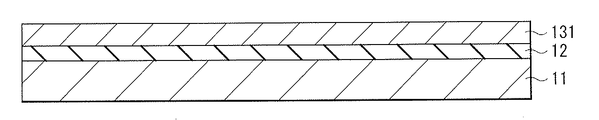
- FIG. 1 shows a cross-sectional configuration of a laminated layer (laminated body 1) for explaining a laminated body and a peeling method thereof according to an embodiment of the present technology.
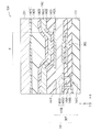
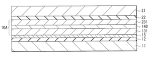
- the laminate 1 has a flexible device (flexible device 10) between a support substrate 11 and a support substrate 21.
- the flexible device 10 is a device in which a functional layer 14 is provided between flexible substrates (flexible substrates 13 and 23).
- This laminated body 1 is formed in the manufacturing process of flexible devices 10, such as a flexible display, for example.
- the flexible substrates 13 and 23 are respectively fixed (fixed) to the support substrates 11 and 21 via the adhesive layers 12 and 22, respectively.
- at least the adhesive layers 12 and 22 are included.
- the support substrate 11 and the support substrate 21 support the flexible substrate 13 and the flexible substrate 23, respectively, to facilitate transportation in the manufacturing process and formation of a functional layer 14 to be described later.
- the support substrate 11 is preferably made of a rigid material such as glass, quartz, or silicon.
- the support substrate 11 is preferably a substrate that is thicker than the flexible substrate 12, and may be 0.4 mm to 2 mm, for example, in terms of mechanical strength and handleability. Further, the linear expansion coefficient of the support substrate 11 is preferably 10 ppm / K or less from the relationship with the substrate 13.
- the adhesive layer 12 and the adhesive layer 22 fix the flexible substrate 13 and the flexible substrate 23 to the support substrate 11 and the support substrate 21, respectively.
- the adhesive layers 12 and 22 are formed, for example, by applying by a printing method such as spin coating, die coating, or gravure.
- general-purpose adhesives and adhesive tapes can be used as a material for the adhesive layers 12 and 22, specific examples include acrylic adhesives (adhesives), epoxy adhesives, siloxane adhesives, urethane adhesives, silane coupling agents, natural rubber adhesives, or synthetic rubber adhesives. .
- one adhesive layer for example, adhesive layer 12
- the other adhesive layer may use an adhesive tape.
- an adhesive tape for example, after attaching the adhesive tape to the support substrate 21 to form the adhesive layer 22, the flexible substrate 23 is fixed by a laminator.
- the flexible substrate 13 and the flexible substrate 23 sandwich the functional layer 14.
- the material of the flexible substrates 13 and 23 preferably has a thermal shrinkage rate of 0.1% or less in order to suppress substrate warpage due to a difference in thermal shrinkage from the support substrates 11 and 21.
- the dimensional change and deformation of the flexible substrates 13 and 23 can be suppressed by setting the linear expansion coefficient to about 0 to 15 ppm / K from the relationship with the support substrates 11 and 21.
- Such materials include polyethylene terephthalate having a thickness of 5 to 200 ⁇ m, polyethylene naphthalate, polyethersulfone, polyetherimide, polyetheretherketone, polyphenylene sulfide, polysulfone, polyarylate, polyimide, polyamide, Plastic materials such as polycarbonate, cellulose triacetate, polyolefin, polystyrene, polyethylene, polypropylene, polymethyl methacrylate, aramid, polyvinyl chloride, polyvinylidene chloride, epoxy resin, phenol resin, urea resin, melamine resin, silicone resin or acrylic resin It is done. It is also possible to use thin glass or thin ceramics as thin as possible to show flexibility.
- the functional layer 14 includes, for example, an electronic circuit layer (TFT layer 141) on which TFTs and various wirings are formed, a display layer (display layer 142), a sealing layer (protective film 142E), a color filter (color filter layer 142G), and the like.
- TFT layer 141 electronic circuit layer
- display layer 142 display layer
- sealing layer protecting film 142E
- color filter layer 142G color filter layer
- a layer having a function for the device is formed (see FIG. 4).
- the functional layer 14 is represented as a single layer and is collectively provided on the substrate 11 side.
- the present invention is not limited to this, and the functional layer 14 may have a multilayer structure, for example. In that case, the functional layers 14A and 14B may be separately provided on the flexible substrates 13 and 23, respectively (see, for example, FIG. 7C).
- the adhesive force here is specifically the adhesion force (surface adhesion force) between the support substrate 11 (or the support substrate 21) and the flexible substrate 13 (or the flexible substrate 23).
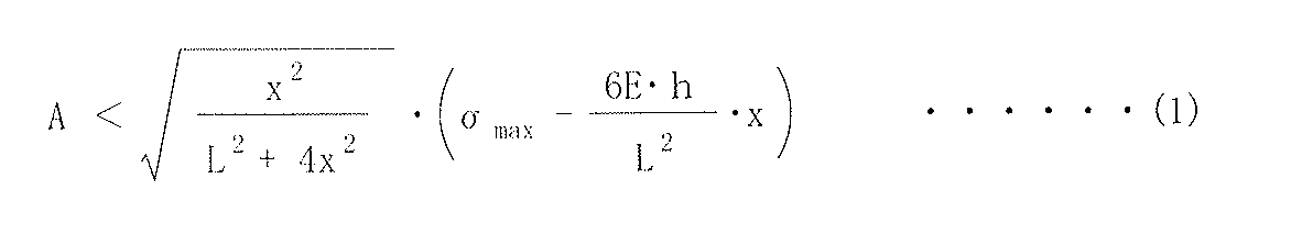
- Formula (1) represents the conditions under which damage does not occur on the substrate (support substrate 11 (or support substrate 21)) that is peeled off at the time of peeling.
- Expressions (2) and (3) represent conditions under which the substrate (support substrate 11 (or support substrate 21)) to be peeled cannot be held by suction due to insufficient suction force during peeling.
- a substrate to be peeled such as the support substrate 11 is a peeling substrate A
- a substrate to be peeled including the flexible substrate 13 and the functional layer 14 is a substrate to be peeled C.
- An adhesive layer that adheres the release substrate A and the substrate to be peeled C is referred to as an adhesive layer B.
- the adhesive force of the adhesive layer B satisfies any of these formulas (1) and / or formulas (2) and (3)
- the release substrate A is easily peeled from the substrate to be peeled B. That is, it becomes possible to peel the support substrate 11 (or the support substrate 21) from the flexible device 10 without damaging the flexible device 10 in the peeling process of the support substrate 11 (or the support substrate 21) described later.
- Each parameter in Formula (1) and Formula (2), (3) is shown in FIG. 2 and FIG.
- Equation (1) is derived as follows.
- Equation (4) is the critical bending stress of the release substrate A
- ⁇ bend is the tensile stress applied to the release substrate A when the release substrate A is bent
- ⁇ bond is the adhesive layer B of the release substrate C. This is the tensile stress applied.
- ⁇ bend can be calculated from the second moment of the release substrate A, and can be expressed by Equation (5).
- L in Formula (5) is the length of the peeling substrate A in the peeling direction
- h is the thickness of the peeling substrate A
- x is the amount of change of the peeling substrate A
- E is the Young's modulus of the peeling substrate A.
- ⁇ bend is expressed by Equation (6) by the decomposition of mechanical force.
- a in Formula (6) is a surface adhesion force between the peeling substrate A and the substrate to be peeled C
- ⁇ is a bending angle.
- Equations (2) and (3) are derived as follows.
- the peeling substrate A has the force shown in FIG. 3 (the peeling substrate A at the peeling starting portion at the time of peeling-the adhesive force (B ') of the substrate C to be peeled, the substrate adsorption to the peeling substrate A at the time of peeling. (Holding) force (C) and the weight ( ⁇ hg) of the release substrate A are applied. From these relationships, the above formula (2) is obtained as a condition for normal peeling at the start of peeling.
- the substrate adsorption (holding) force that is, the peeling force C in the vertical direction (Z-axis direction) at the time of peeling becomes a small value in the case of holding in a vacuum, and between the peeling substrate A and the peeling substrate C.
- the length l of the peeling start portion represents a relationship as shown in FIG. In FIG. 3, at least a length of 1 from the substrate end in the drawing must satisfy the formula (2).
- r is a radius of curvature
- d is an allowable substrate protrusion and a warp amount
- z is a distance extending from the end of the release substrate A toward the center of the curvature circle and intersecting with the release substrate A in a warped state.
- the length 1 required at the start of peeling can be defined by the radius of curvature r, the allowable substrate protrusion, and the warpage amount d.
- the radius of curvature is determined by the specifications of the apparatus for peeling the release substrate A and the physical properties of the release substrate A.
- the allowable substrate protrusion and the warpage amount d are also defined by the specifications of the equipment and the physical properties of the release substrate A. That is, the conditions under which the peeling substrate A is normally peeled with a sufficient adsorbing force are defined by the adhesive strength B ′ between the peeling substrate A and the substrate C to be peeled at the peeling start portion and the length l of the peeling start portion. Is done.
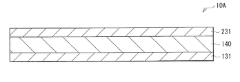
- FIG. 4 illustrates a cross-sectional configuration of a display device (display device 10A) as an example of the flexible device 10 in FIG.
- the display device 10A is, for example, a flexible ultra-thin organic light emitting color display, and a functional layer 140 (for example, a TFT layer 141 and a display layer 142 between a flexible driving substrate 131 and a counter substrate 231). 8) is provided.
- the drive substrate 131 is fixed on the support substrate 11, and on the drive substrate 131, the lower electrode 142A, the organic layer 142B, the upper electrode 142C, and the protective layer that constitute the TFT layer 141 and the display layer 142 are provided.
- a display body made of the film 142D or the like is provided (functional layer 140A).
- the counter substrate 231 is fixed on the support substrate 21, and a color filter 142G and a sealing film 142E constituting the display layer 142 are provided on the counter substrate 231 (functional layer 140B).
- the functional layer 140A and the functional layer 140B are opposed to each other, and the color filter layer 142G and the protective film 142D are bonded to each other through the sealing film 142E. Is manufactured.
- FIG. 4 schematically shows the structure of the display device 10A and may differ from the actual size and shape.
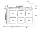
- FIG. 5 illustrates the overall configuration of the display device 10A.
- the display device 10A has a display area 310 at the center on the drive substrate 131.
- a signal line drive circuit 320 and a scanning line drive circuit 330 are provided. Is provided.
- a plurality of pixels 40R, 40G, and 40B that are two-dimensionally arranged in a matrix and a pixel driving circuit 340 for driving them are formed.
- a plurality of signal lines 320A are arranged in the column direction, and a plurality of scanning lines 330A are arranged in the row direction.
- Pixels 40R, 40G, and 40B are provided corresponding to each intersection of each signal line 320A and each scanning line 330A.
- the pixels 40R, 40G, and 40B are pixels that emit red, green, and blue, respectively.
- Each signal line 320A is connected to the signal line driving circuit 320
- each scanning line 330A is connected to the scanning line driving circuit 330.
- the signal line driving circuit 320 supplies a signal voltage of a video signal corresponding to luminance information supplied from a signal supply source (not shown) to the selected pixels 40R, 40G, and 40B via the signal line 320A. It is. A signal voltage from the signal line driver circuit 320 is applied to the signal line 320A.
- the scanning line driving circuit 330 includes a shift register or the like that sequentially shifts (transfers) the start pulse in synchronization with the input clock pulse.
- the scanning line driving circuit 330 scans them in units of rows when writing video signals to the pixels 40R, 40G, and 40B, and sequentially supplies the scanning signals to the respective scanning lines 330A.
- a scanning signal from the scanning line driving circuit 330 is supplied to the scanning line 330A.
- the pixel drive circuit 340 is provided in the TFT layer 141. As shown in FIG. 6, the pixel driving circuit 340 is an active driving circuit having a driving transistor Tr1 and a writing transistor Tr2, a storage capacitor 30C therebetween, and an organic light emitting element EL.
- Each layer of the display device 10A has the following configuration, for example.
- the driving substrate 131 and the counter substrate 231 are the flexible substrate 13 and the flexible substrate 23, and have the same configuration.
- the TFT layer 141 is provided with, for example, a TFT composed of a gate electrode 141A, a gate insulating film 141B, a semiconductor layer 141C as a channel layer, and source / drain electrodes 141D (141D1, 141D2). . These are formed through a film forming and etching process by a CVD (Chemical Vapor Deposition) method or the like.
- the source / drain electrodes 141D (141D1, 141D2) are covered with a planarization layer 141E made of an insulating resin material such as polyimide.
- the TFT may be either an inorganic TFT using an inorganic semiconductor layer or an organic TFT using an organic semiconductor layer.
- the TFT has a function as a switching element for selecting a pixel.
- the TFT layer 141 is not limited to the TFT, and other electronic devices such as an optical functional layer such as a 3D display optical device, a touch panel, and a moth eye, or a MEMS device may be formed.
- the display layer 142 includes, from the drive substrate 131 (planarization layer 141E) side, a lower electrode 142A as an anode electrode, an organic layer 142B including a light emitting layer, and an upper electrode 142C as a cathode electrode.
- the upper electrode 142C is covered with a protective film 142D, and the counter substrate 230 including the color filter 142G is provided on the protective film 142D with the sealing film 142E interposed therebetween.
- the organic layer 142B has, for example, a hole injection layer, a hole transport layer, a light emitting layer, and an electron transport layer in this order from the lower electrode 142A side.
- This light emitting layer may be provided for each of the pixels 40R, 40G, and 40B, or may be provided in common for each of the pixels 40R, 40G, and 40B. Layers other than the light emitting layer may be provided as necessary.
- the protective film 142D is for preventing moisture from entering the organic layer 142B, for example, aluminum oxide (Al 2 O 3 ), silicon oxide (SiO), silicon nitride (SiN), or oxynitride It is formed of an insulating material such as silicon (SiON).
- the pixels 40R, 40G, and 40B are separated by a pixel separation film 142F, and the pixel region P (light emitting region) of the pixels 40R, 40G, and 40B is defined by the pixel separation film 142F.
- the organic layer 142B may be formed as a solid film on the entire surface of the light emitting region P or the driving substrate 131.
- the color filter layer 142G has, for example, a color filter corresponding to the pixels 40R, 40G, and 40B and a black matrix between the color filters (not shown).
- the color filter layer 142G is provided on the counter substrate 231 side as described above, and is bonded to the display layer 142 through the sealing film 142E.
- the sealing film 142E is made of, for example, a material used for the protective film 142D, an ultraviolet (UV) curable resin, a thermosetting resin, or the like.
- Such a display device 10A can be manufactured as follows, for example.
- a pressure-sensitive adhesive layer 12 is formed by applying a pressure-sensitive adhesive satisfying the above formula (1) and / or formulas (2) and (3) to a support substrate 11 made of glass, for example. Form.
- a flexible drive substrate 131 is fixed on the adhesive layer 12, and then heat treatment is performed at 120 to 250 ° C. for 10 to 60 minutes, for example. By this heat treatment, thermal contraction of the drive substrate 131 is forcibly induced, and the behavior of the drive substrate 131 in the subsequent process is stabilized.
- the adhesive force of the adhesive which comprises the adhesion layer 12 is also stabilized.
- the TFT substrate 141 and a part of the display layer 142 are formed on the driving substrate 131.
- the functional layer 140A is laminated in this order.
- the functional layer 140B including the counter substrate 231 and the color filter layer 142G is formed on the support substrate 21 made of, for example, glass via an adhesive, and the functional layer 140A and the functional layer 140B are provided.
- the support substrate 11 and the support substrate 21 are arranged to face each other.
- the adhesive which comprises the adhesion layer 22 by the side of the opposing substrate 21 may satisfy
- the support substrate 11 and the support substrate 21 are bonded to each other with the sealing film 142 ⁇ / b> E and a sealant (not illustrated), and the laminate including the display device 10 ⁇ / b> A that is the flexible device 10.
- the picking tape A is attached to the peeling start portion, and the support substrate 11 is peeled by pulling in the arrow direction. Or you may peel by rotating the vacuum stage with a curvature. Note that the peeling method is not limited to these, and other methods may be used, and any type of adhesive stage or electrostatic force may be used.
- the support substrate 21 is peeled in the same manner. Thereby, the display device 10A as shown in FIG. 8C is completed.
- a scanning signal is supplied from the scanning line driving circuit 330 to the respective pixels 40R, 40G, and 40B via the gate electrode 141A of the writing transistor Tr2, and an image signal is received from the signal line driving circuit 320. It is held in the holding capacitor 30C via the write transistor Tr2. That is, the driving transistor Tr1 is controlled to be turned on / off according to the signal held in the holding capacitor 30C, whereby a driving current is injected into the pixels 40R, 40G, and 40B, and holes and electrons are recombined to emit light. Occur. This light passes through the upper electrode 142C, the protective film 142D, the sealing film 142E, and the counter substrate 230 and is extracted.
- the driving substrate 131 and the counter substrate 231 that constitute the display device 10A that is the flexible device 10 are used as the supporting substrate 11 and the supporting substrate 21, respectively.
- the pressure-sensitive adhesive layer 12 and the pressure-sensitive adhesive layer 22 that adheres to each other at least the pressure-sensitive adhesive layer that peels first (for example, the pressure-sensitive adhesive layer 12) satisfies the above formula (1) and / or formulas (2) and (3). It is formed using a pressure-sensitive adhesive. This makes it possible to peel the support substrate 11 without damaging it and without applying a load to the functional layer 140.
- a flexible device such as a so-called flexible display in which various devices such as display elements are formed on a flexible substrate is an existing one after fixing the flexible substrate to a rigid substrate such as glass. Since a display device manufacturing line can be used, the display device can be manufactured at low cost. However, it is difficult to peel off a glass substrate from a device sandwiched by a rigid substrate (for example, a glass substrate), such as glass-glass. For example, the glass substrate may be damaged during peeling, and may not be peeled off. It was. Or there existed a problem that it was not able to be made to peel because the adsorption
- a metal layer is provided on a glass substrate and the metal layer is irradiated with a laser to peel off, for example, a pressure-sensitive adhesive is applied only to the outer peripheral portion of a flexible substrate.
- fixing methods have been used, there have been problems such as an increase in cost due to the use of a laser, deterioration of a functional layer due to laser irradiation, or misalignment due to insufficient fixing force.
- the adhesive layer (adhesive layer 12) between the substrates to be peeled first (here, the drive substrate 131 (flexible substrate 13) and the support substrate 11) is the above formula.
- the support substrate 11 and the drive substrate 131 (flexible substrate 13) are mechanically peeled off by preparing to have an adhesive force satisfying at least one of (1) and formulas (2) and (3). Is possible.
- an adhesive is provided between the support substrate 11 and the drive substrate 131 (flexible substrate 13).
- the pressure-sensitive adhesive layer 12 satisfying at least one of the above formulas (1), (2), and (3) was formed.
- the separation can be performed without performing treatment such as laser irradiation, it is possible to prevent the TFT layer 141, the display layer 142, and the like from deteriorating on the support substrate 11. Furthermore, since the adhesive layer 12 can be applied and fixed to the entire surface of the support substrate 11 and the drive substrate 131, a high-definition display device can be manufactured.
- Modification> (Modification 1) 9A to 9C show another example (modification example 1) of the method for manufacturing the display device 10A described in the above embodiment.
- the adhesive force between the pressure-sensitive adhesive layer (for example, the pressure-sensitive adhesive layer 12) adjusted so as to satisfy the above formula (1) and / or the formulas (2) and (3) and the flexible substrate 13 is further increased.
- Weak release layer 15 is formed.
- the display device 10A is manufactured in the same manner as in the above embodiment.
- the release layer 15 reduces the adhesive force between the adhesive layer 12 and the flexible substrate 13 and is made of, for example, an inorganic material. Specific examples include silicon nitride (SiN x ) and silicon oxide (SiO 2 ).
- the thickness of the release layer 15 is preferably 50 nm or more and 500 nm or less, for example.
- the release layer 15 may adhere to the flexible substrate 13 side in the peeling step. For example, when the release layer 15 is provided on the flexible substrate side in the light emitting direction, if the film thickness is too thick, the transmittance decreases, and the organic layer A thinner one is preferable because it blocks light emitted from the EL and lowers the light emission efficiency.
- the display device 10A according to this modification is manufactured as follows.
- a release layer 15 is formed on the drive substrate 131 by using, for example, a CVD method to form, for example, a SiN film.
- an adhesive that satisfies the above formula (1) and / or formulas (2) and (3) is applied on the support substrate 11 to form the adhesive layer 12.
- the adhesive layer 12 and the release layer 15 that are arranged to face each other are bonded together.
- the counter substrate 231 fixed to the support substrate 21 via the adhesive layer 22 is bonded to the support substrate 21 as shown in FIG. 9C.
- a laminated body including the display device 10A which is the flexible device 10 is formed.
- the support substrate 11 and the support substrate 21 are peeled off by using the same method as in the above embodiment, whereby the display device 10A is completed.
- the adhesive force between the adhesive layer 12 adjusted to satisfy the above formula (1) and / or the formulas (2) and (3) and the drive substrate 131 is weaker.
- the amount of adhesion between the drive substrate 131 and the adhesive layer 12 is reduced, and the support substrate 11 can be peeled off with a weaker force. That is, at the time of peeling, deterioration of characteristics due to a load on the functional layer 140 such as the display layer 142 is suppressed, and a highly reliable flexible device can be provided.
- the separation is performed between the drive substrate 131 and the release layer 15, adhesion of the adhesive to the drive substrate 131 side after the separation is reduced. Therefore, the visibility of the display device 10A is improved and adhesion of dust and the like due to the remaining adhesive is prevented.
- the release layer 15 is provided on the one support substrate 11 side, but may be provided on both the other support substrate 21 side.
- Modification 2 10A to 10C show another example (Modification 2) of the method for manufacturing the display device 10A described in the above embodiment and Modification 1.
- FIG. 1 for example, the adhesive force is weaker between the support substrate 11 and the adhesive layer (for example, the adhesive layer 12) adjusted to satisfy the above formula (1) and / or the formulas (2) and (3).
- a release layer 15 is formed.
- the display device 10A is manufactured in the same manner as in the above embodiment.
- the display device 10A according to this modification is manufactured as follows.
- a release layer 15 and an adhesive layer 12 are formed in this order on a support substrate 11.
- a CVD method is used to form a release layer 15 by forming, for example, a SiN film on the support substrate 11, and then the above formula (1) and / or on the release layer 15.
- the pressure-sensitive adhesive satisfying the formulas (2) and (3) is applied to form the pressure-sensitive adhesive layer 12.
- the functional layer 140 ⁇ / b> A is formed.
- a counter substrate 231 that is separately fixed on the support substrate 21 via the adhesive layer 22 is bonded to form a laminate including the display device 10A that is the flexible device 10 as shown in FIG. 10C. .
- the support substrate 11 and the support substrate 21 are peeled off by using the same method as in the above embodiment, whereby the display device 10A is completed.
- the adhesive force is weaker between the support substrate 11 and the adhesive layer 12 adjusted to satisfy the above formula (1) and / or the formulas (2) and (3).
- a release layer 15 was formed.
- the adhesion amount of the support substrate 11 and the adhesion layer 12 is reduced, and it becomes possible to peel the support substrate 11 with a weaker force. That is, for example, it is possible to suppress damage to the functional layer 14 such as the display layer 142 and to provide a highly reliable flexible device.
- the release layer 15 is provided on one support substrate side.
- the release layer 15 may be provided on the other support substrate (here, the support substrate 21), or both.
- the support substrates 11 and 21 and the adhesive layers 12 and 22 may be provided.
- the display device 10A may be manufactured by combining the first modification and the second modification.
- the release layer 15 is provided between the support substrate 11 and the adhesive layer 12 on the support substrate 11 side
- the release layer 21 is formed between the adhesive layer 22 and the counter substrate 231 on the support substrate 21 side. Or vice versa.
- the physical properties such as the adhesive strength of the adhesive layer 12 satisfying the above formulas (1) and / or (2) and (3) are controlled by external stimuli (for example, light, heat, electromagnetic force, etc.). Also good.
- Modification 3 11A to 12B show a part of the manufacturing process of the display device 1 according to the third modification of the above embodiment.
- this modification for example, a process in which a plurality of flexible devices 10 to be the display device 10A, for example, are formed on a large substrate and the substrates are bonded together and then divided individually will be described.
- the display device 10A will be described as an example.
- a functional layer for example, a color filter and a sealing film
- a flexible substrate for example, a counter substrate
- a functional substrate is cut into the flexible substrate, and a flexible substrate (for example, a driving substrate on which an organic film including a light-emitting layer is formed) fixed to the other supporting substrate is bonded.
- the support substrates are respectively peeled off and divided along the cuts, whereby a plurality of flexible devices can be manufactured collectively.
- the functional layer may be damaged, such as cracks, and the reliability of the device may be reduced.
- a plurality of flexible devices 10 are collectively manufactured as follows. First, as shown in FIG. 11A, on the large counter substrate 231 fixed on the support substrate 21 via an adhesive layer 22 (not shown here), as the functional layer 14, here the color filter layer 142G. A plurality of are formed. Subsequently, as shown in FIG. 11B, cuts CL are made at the peripheral edge of each color filter 142G. Next, as shown in FIG. 11C, after forming a sealing film 142E on the color filter 142G, as shown in FIG. 12A, the support substrate 11 is provided with an adhesive layer 12 (omitted here).
- the driving substrate 131 which is fixed and separately formed with the TFT layer 141, the organic film 142B, and the like, is bonded. Finally, as shown in FIG. 12B, the support substrate 11 and the support substrate 21 are peeled off, and the plurality of flexible devices 10 are divided along the cuts CL, whereby a plurality of display devices 10A are manufactured. .
- FIG. 13 schematically shows a cross-sectional configuration of the flexible device 10 taken along the line II in FIG. 12A.
- damage to the sealing film 142E is prevented, and the sealing film 142E is formed on the end face of the color filter 142G.
- the manufacturing process on the counter substrate 231 side has been described as an example, but the present invention can also be applied to the manufacturing process on the drive substrate 131 side. In this case, for example, the upper electrode 142C corresponding to the functional layer is formed, and then a cut is made, and then the protective film 142D is formed.
- the color filter 142G (or the organic film 142B and the upper electrode 142C) are formed on the counter substrate 231 (or the drive substrate 131) fixed to the support substrate 21 (or the support substrate 11). ), A cut CL is made in the color filter 142G and the counter substrate 231 (or from the upper electrode 142C to the drive substrate 131), and then the seal that protects the color filter 142 (or the organic film 142B or the like). A film 142E (or a protective film 142D) is formed. Thereby, damage to the sealing film 142E (or the protective film 142D) is prevented, and the manufacturing yield is improved.
- a sealing film 142G (or protective film 142D) made of an inorganic material such as SiN or Al 2 O 3 is formed on the end faces of the color filter 142G and the counter substrate 231 (or the organic film 142B, the TFT layer 141, etc.). Therefore, intrusion of moisture or the like into the layer formed of the organic material is suppressed, and the reliability is improved.
- the present invention is not limited to this, and the manufacturing method of the present modified example can be applied to a single flexible device 10 from a single substrate. It can also be applied to the manufacture of
- the display device 10A manufactured using the method of the present embodiment and the first to third modifications is input from the outside, such as a television device, a digital camera, a notebook personal computer, a mobile terminal device such as a mobile phone, or a video camera.
- the present invention can be applied to display devices of electronic devices in various fields that display the generated video signal or the video signal generated inside as an image or video.
- the electronic book includes, for example, a display unit 110, a non-display unit 120, and an operation unit 130.
- the operation unit 130 may be provided on the front surface of the non-display unit 120 as illustrated in FIG. 14A or may be provided on the upper surface as illustrated in FIG. 14B.
- the display unit 110 is configured by the display device 1.
- the display device 1 may be mounted on a PDA (Personal Digital Assistants) having the same configuration as the electronic book shown in FIGS. 14A and 14B.
- PDA Personal Digital Assistants
- FIG. 15 shows the appearance of a tablet personal computer.
- the tablet personal computer has, for example, a touch panel unit 310 and a housing 320, and the touch panel unit 310 is configured by the display device 1.
- the present technology has been described with the embodiment and the first to third modifications, the present technology is not limited to the above-described embodiment and the like, and various modifications can be made.
- the display device 10A includes the TFT layer 141, that is, the case where the display device is an active matrix display device has been described, but the display device 10A may be a passive matrix type.
- the materials and thicknesses of the respective parts described in the above embodiments and the application examples thereof and the forming method and forming conditions are not limited, and other materials and thicknesses may be used, or other forming methods and It is good also as formation conditions.
- the adhesive layers 12 and 22 are formed on the entire surfaces of the support substrates 11 and 21 has been described.
- the present invention is not limited to this.
- the pattern may be formed so that no adhesive is present in the part.
- a display device provided with three types of pixels 2R, 2G, and 2B made of red, green, and blue as an example has been described. Yellow pixels may be combined.
- the display device 10A is not only a display device including an organic EL element but also a display device including various display elements such as an inorganic EL element, a liquid crystal element, and an electrophoretic display element. Applicable.
- the display device 10A may include other layers.
- the inorganic film made of the same material as the release layer 15 on the functional layer 14 side such as the display layer 142 of each of the flexible substrates 13 and 23, the inorganic film functions as a barrier layer. It becomes possible to reduce the intrusion of moisture into the organic film constituting the layer 142. Thereby, reliability can be improved.
- this technique can also take the following structures. (1) Forming a first adhesive layer having an adhesive force on at least one of the following formula (1) and formulas (2) and (3) on the first substrate; Fixing the second substrate on the first adhesive layer; Forming a first functional layer on the second substrate; Peeling the first substrate from the second substrate.
- the first adhesive layer is the method for manufacturing a multilayer substrate according to (1), wherein both the formula (1) and the formulas (2) and (3) are satisfied.
Landscapes
- Engineering & Computer Science (AREA)
- Power Engineering (AREA)
- Manufacturing & Machinery (AREA)
- Physics & Mathematics (AREA)
- Condensed Matter Physics & Semiconductors (AREA)
- General Physics & Mathematics (AREA)
- Computer Hardware Design (AREA)
- Microelectronics & Electronic Packaging (AREA)
- Electroluminescent Light Sources (AREA)
- Laminated Bodies (AREA)
Abstract
The present invention discloses a method for separating a laminate, which comprises: a step for forming a first adhesive layer, which has an adhesive power satisfying formula (1) and at least one of formulae (2) and (3), on a first substrate; a step for firmly bonding a second substrate onto the adhesive layer; a step for forming a first function layer on the second substrate; and a step for separating the first substrate from the second substrate.
Description
本技術は、例えば、剛性を有する基板と可撓性を有する基板とが貼り合わされた積層体および積層体の剥離方法ならびにこれを用いた可撓性デバイスの製造方法に関する。
The present technology relates to, for example, a laminate in which a rigid substrate and a flexible substrate are bonded together, a method for peeling the laminate, and a method for manufacturing a flexible device using the laminate.
フレキシブルディスプレイ等の可撓性を有する表示装置は、例えば以下のように製造される。まず、例えば一対のガラス等の剛性を有する基板(支持基板)にそれぞれ可撓性を有する基板(可撓性基板)を固定し、各可撓性基板上でTFT(Thin Film Transistor)層や表示層あるいはカラーフィルタ等の機能層を形成する。続いて、これら機能層を対向させて貼り合わしたのち、支持基板を可撓性基板から剥がすことによってフレキシブルディスプレイが完成する(例えば、特許文献1参照)。
For example, a flexible display device such as a flexible display is manufactured as follows. First, for example, a flexible substrate (flexible substrate) is fixed to a rigid substrate (support substrate) such as a pair of glass, and a TFT (ThinThFilmorTransistor) layer or display on each flexible substrate. A functional layer such as a layer or a color filter is formed. Subsequently, after these functional layers are bonded to face each other, the support substrate is peeled off from the flexible substrate to complete a flexible display (see, for example, Patent Document 1).
可撓性基板と支持基板との剥離方法としては、例えば支持基板上に金属層を設け、この金属層にレーザを照射して剥離する方法(例えば、特許文献2参照)や、可撓性基板の一部(例えば、外周部)のみに接着剤を塗布することで剥離を容易にする方法が開示されている。
As a peeling method between the flexible substrate and the support substrate, for example, a method in which a metal layer is provided on the support substrate and the metal layer is irradiated with a laser to peel off (see, for example, Patent Document 2), or a flexible substrate is used. A method is disclosed in which peeling is facilitated by applying an adhesive only to a part (for example, the outer peripheral portion).
しかしながら、特許文献2のようにレーザを用いる場合には、レーザを用いることによるコストの増加やレーザ照射によって発生する熱により機能層が劣化するという問題があった。また、可撓性基板の一部のみを固定する場合には、固定が十分ではないため位置ずれ等が起こりやすく高精細な機能層の形成が困難であった。
However, when a laser is used as in Patent Document 2, there are problems that the cost is increased due to the use of the laser and that the functional layer is deteriorated by heat generated by laser irradiation. Further, when only a part of the flexible substrate is fixed, since the fixing is not sufficient, misalignment or the like is likely to occur, and it is difficult to form a high-definition functional layer.
従って、機能層を劣化させることなく、容易且つ安価に剥離することが可能な積層体および積層体の剥離方法ならびにこれを用いた可撓性デバイスの製造方法を提供することが望ましい。
Therefore, it is desirable to provide a laminate that can be easily and inexpensively peeled without degrading the functional layer, a method for peeling the laminate, and a method for manufacturing a flexible device using the laminate.
本技術の一実施の形態に係る積層体の剥離方法は、第1基板上に、粘着力が下記式(1)および式(2),(3)の少なくとも一方を満たす第1粘着層を形成することと、第1粘着層上に第2基板を固着することと、第2基板上に第1機能層を形成することと、第1基板を第2基板から剥離することとを含むものである。
In the method for peeling a laminate according to an embodiment of the present technology, a first adhesive layer whose adhesive strength satisfies at least one of the following formulas (1), (2), and (3) is formed on a first substrate. And affixing the second substrate on the first adhesive layer, forming the first functional layer on the second substrate, and peeling the first substrate from the second substrate.


本技術の一実施の形態に係る可撓性デバイスの製造方法は、上記本技術の積層体の剥離方法における第2基板として可撓性を有する基板を用いるものである。
A method for manufacturing a flexible device according to an embodiment of the present technology uses a flexible substrate as the second substrate in the laminate peeling method of the present technology.
本技術の一実施の形態に係る積層体は、剛性を有する第1基板と、可撓性を有する第2基板と、粘着力が下記式(1)を満たす、第1基板と第2基板との間に設けられた粘着層とを備えたものである。
A laminated body according to an embodiment of the present technology includes a first substrate having rigidity, a second substrate having flexibility, a first substrate, a second substrate, and an adhesive force satisfying the following formula (1): And an adhesive layer provided between the two.
本技術の一実施の形態に係る積層体および積層体の剥離方法ならびに可撓性デバイスの製造方法では、第1基板と第2基板との間に、粘着力が上記式(1)および式(2),(3)の少なくとも一方を満たす粘着層を形成することにより、機械的に第1基板と第2基板とを剥離することが可能となる。
In the laminate, the laminate peeling method, and the flexible device manufacturing method according to an embodiment of the present technology, the adhesive force between the first substrate and the second substrate is expressed by the above formula (1) and formula ( By forming an adhesive layer that satisfies at least one of 2) and (3), the first substrate and the second substrate can be mechanically separated.
本技術の一実施の形態に係る積層体および積層体の剥離方法ならびに可撓性デバイスの製造方法によれば、第1基板と第2基板との間に、上記式(1)および式(2),(3)の少なくとも一方を満たす粘着力の粘着層を形成するようにしたので、機械的に第1基板と第2基板とが剥離される。即ち、剥離時に機能層を劣化させることなく、容易且つ安価に第1基板と第2基板とを剥離することが可能となる。なお、ここに記載された効果は必ずしも限定されるものではなく、本開示中に記載されたいずれの効果であってもよい。
According to the laminate, the laminate peeling method, and the flexible device manufacturing method according to an embodiment of the present technology, the above formulas (1) and (2) are provided between the first substrate and the second substrate. ) And (3), the pressure-sensitive adhesive layer satisfying at least one of them is formed, so that the first substrate and the second substrate are mechanically separated. That is, it is possible to peel the first substrate and the second substrate easily and inexpensively without deteriorating the functional layer at the time of peeling. Note that the effects described here are not necessarily limited, and may be any effects described in the present disclosure.
以下、本技術の実施の形態について、図面を参照して詳細に説明する。なお、説明は以下の順序で行う。
1.実施の形態(支持基板と可撓性デバイスとの間に式(1)および式(2),(3)を満たす粘着層を設けた例)
2.変形例 変形例1(粘着層と可撓性デバイスとの間に離型層を設けた例)
変形例2(支持基板と粘着層との間に離型層を設けた例)
変形例3(予め、可撓性基板に切り込みを入れて分割する例)
3.適用例 Hereinafter, embodiments of the present technology will be described in detail with reference to the drawings. The description will be given in the following order.
1. Embodiment (Example in which an adhesive layer satisfying the formulas (1), (2), and (3) is provided between the support substrate and the flexible device)
2. Modification Example Modification 1 (Example in which a release layer is provided between the adhesive layer and the flexible device)
Modification 2 (Example in which a release layer is provided between the support substrate and the adhesive layer)
Modification 3 (Example in which a flexible substrate is cut and divided in advance)
3. Application examples
<1.実施の形態>
図1は、本技術の一実施の形態に係る積層体およびその剥離方法を説明するための積層層(積層体1)の断面構成を表したものである。この積層体1は、支持基板11と支持基板21との間に可撓性を有するデバイス(可撓性デバイス10)を有するものである。可撓性デバイス10は、可撓性を有する基板(可撓性基板13,23)の間に機能層14が設けられたものである。この積層体1は、例えばフレキシブルディスプレイ等の可撓性デバイス10の製造過程において形成されるものである。可撓性基板13,23はそれぞれ支持基板11,21に、それぞれ粘着層12,22を介して固定(固着)されており、本実施の形態の積層体1では、粘着層12,22の少なくとも一方が後述する式(1)を満たす粘着力を有している。また、このような積層体1を剥離する際には、粘着層12,22の少なくとも一方がこの式(1)または後述する式(2),(3)のどちらかあるいは両方を満たす粘着力を有するように調製することによって、可撓性デバイス10から支持基板11(および/また支持基板21)を容易且つ安価に剥離することが可能となる。 <1. Embodiment>
FIG. 1 shows a cross-sectional configuration of a laminated layer (laminated body 1) for explaining a laminated body and a peeling method thereof according to an embodiment of the present technology. The laminate 1 has a flexible device (flexible device 10) between asupport substrate 11 and a support substrate 21. The flexible device 10 is a device in which a functional layer 14 is provided between flexible substrates (flexible substrates 13 and 23). This laminated body 1 is formed in the manufacturing process of flexible devices 10, such as a flexible display, for example. The flexible substrates 13 and 23 are respectively fixed (fixed) to the support substrates 11 and 21 via the adhesive layers 12 and 22, respectively. In the laminate 1 of the present embodiment, at least the adhesive layers 12 and 22 are included. One has an adhesive force that satisfies the formula (1) described below. Moreover, when peeling such a laminated body 1, the adhesive force in which at least one of the adhesion layers 12 and 22 satisfy | fills this formula (1), formula (2), (3) mentioned later, or both is satisfy | filled. By preparing so that it may have, it becomes possible to peel the support substrate 11 (and / or the support substrate 21) from the flexible device 10 easily and inexpensively.
図1は、本技術の一実施の形態に係る積層体およびその剥離方法を説明するための積層層(積層体1)の断面構成を表したものである。この積層体1は、支持基板11と支持基板21との間に可撓性を有するデバイス(可撓性デバイス10)を有するものである。可撓性デバイス10は、可撓性を有する基板(可撓性基板13,23)の間に機能層14が設けられたものである。この積層体1は、例えばフレキシブルディスプレイ等の可撓性デバイス10の製造過程において形成されるものである。可撓性基板13,23はそれぞれ支持基板11,21に、それぞれ粘着層12,22を介して固定(固着)されており、本実施の形態の積層体1では、粘着層12,22の少なくとも一方が後述する式(1)を満たす粘着力を有している。また、このような積層体1を剥離する際には、粘着層12,22の少なくとも一方がこの式(1)または後述する式(2),(3)のどちらかあるいは両方を満たす粘着力を有するように調製することによって、可撓性デバイス10から支持基板11(および/また支持基板21)を容易且つ安価に剥離することが可能となる。 <1. Embodiment>
FIG. 1 shows a cross-sectional configuration of a laminated layer (laminated body 1) for explaining a laminated body and a peeling method thereof according to an embodiment of the present technology. The laminate 1 has a flexible device (flexible device 10) between a
支持基板11および支持基板21は、それぞれ可撓性基板13および可撓性基板23を支持して製造過程における運搬および後述する機能層14の形成を容易にするものである。支持基板11は、例えばガラス,石英あるいはシリコン等の剛性材料により構成することが好ましい。支持基板11は、可撓性基板12よりも厚い基板を用いることが好ましく、例えば、機械的強度や取り扱い性の点から0.4mm~2mmであればよい。また、支持基板11の線膨張係数は、基板13との関係から10ppm/K以下であることが好ましい。
The support substrate 11 and the support substrate 21 support the flexible substrate 13 and the flexible substrate 23, respectively, to facilitate transportation in the manufacturing process and formation of a functional layer 14 to be described later. The support substrate 11 is preferably made of a rigid material such as glass, quartz, or silicon. The support substrate 11 is preferably a substrate that is thicker than the flexible substrate 12, and may be 0.4 mm to 2 mm, for example, in terms of mechanical strength and handleability. Further, the linear expansion coefficient of the support substrate 11 is preferably 10 ppm / K or less from the relationship with the substrate 13.
粘着層12および粘着層22は、可撓性基板13および可撓性基板23を支持基板11および支持基板21にそれぞれ固定するものであり、支持基板11(または支持基板21)と可撓性基板13(または可撓性基板23)との、例えば接触面の全面に設けられている。粘着層12,22は、例えばスピンコート法,ダイコートまたはグラビア等の印刷法で塗布することにより形成する。粘着層12,22の材料としては、汎用的な粘着剤および粘着テープを用いることができる。具体的には、例えばアクリル系接着剤(粘着剤),エポキシ系接着剤,シロキサン系接着剤,ウレタン系接着剤,シランカップリング剤,天然ゴム系接着剤または合成ゴム系接着剤等が挙げられる。
The adhesive layer 12 and the adhesive layer 22 fix the flexible substrate 13 and the flexible substrate 23 to the support substrate 11 and the support substrate 21, respectively. The support substrate 11 (or the support substrate 21) and the flexible substrate 13 (or flexible substrate 23), for example, is provided on the entire contact surface. The adhesive layers 12 and 22 are formed, for example, by applying by a printing method such as spin coating, die coating, or gravure. As a material for the adhesive layers 12 and 22, general-purpose adhesives and adhesive tapes can be used. Specific examples include acrylic adhesives (adhesives), epoxy adhesives, siloxane adhesives, urethane adhesives, silane coupling agents, natural rubber adhesives, or synthetic rubber adhesives. .
なお、本実施の形態では、一方の粘着層(例えば、粘着層12)が後述する式(1)および式(2),(3)のどちらかあるいは両方を満たす粘着力を有するものであれば、他方の粘着層(例えば、粘着層22)は、粘着テープを用いてもよい。粘着テープを用いる場合には、例えば支持基板21に粘着テープを添付して粘着層22を形成したのち、ラミネータで可撓性基板23を固定する。
In this embodiment, as long as one adhesive layer (for example, adhesive layer 12) has an adhesive force satisfying either or both of formulas (1), (2), and (3) described later. The other adhesive layer (for example, adhesive layer 22) may use an adhesive tape. When using an adhesive tape, for example, after attaching the adhesive tape to the support substrate 21 to form the adhesive layer 22, the flexible substrate 23 is fixed by a laminator.
可撓性基板13および可撓性基板23は、機能層14を挟持するものである。可撓性基板13,23の材料としては、支持基板11,21との熱収縮差による基板反りを抑制するために、熱収縮率が0.1%以下であることが好ましい。また、支持基板11,21との関係から線膨張係数を0~15ppm/K程度とすることで、可撓性基板13,23の寸法変化と変形を抑制することができる。このような材料としては、具体的には、例えば厚み5~200μmのポリエチレンテレフタレート,ポリエチレンナフタレート,ポリエーテルスルホン,ポリエーテルイミド,ポリエーテルエーテルケトン,ポリフェニレンスルフィド,ポリスルホン,ポリアリレート,ポリイミド,ポリアミド,ポリカーボネート,セルローストリアセテート,ポリオレフィン,ポリスチレン,ポリエチレン,ポリプロピレン,ポリメチルメタクリレート,アラミド,ポリ塩化ビニル,ポリ塩化ビニリデン,エポキシ樹脂,フェノール樹脂,ユリア樹脂,メラミン樹脂,シリコン樹脂またはアクリル樹脂等のプラスチック材料が挙げられる。なお、薄層ガラスあるいは薄層セラミックス等を可撓性を示す程度まで薄くして使用することも可能である。
The flexible substrate 13 and the flexible substrate 23 sandwich the functional layer 14. The material of the flexible substrates 13 and 23 preferably has a thermal shrinkage rate of 0.1% or less in order to suppress substrate warpage due to a difference in thermal shrinkage from the support substrates 11 and 21. In addition, the dimensional change and deformation of the flexible substrates 13 and 23 can be suppressed by setting the linear expansion coefficient to about 0 to 15 ppm / K from the relationship with the support substrates 11 and 21. Specific examples of such materials include polyethylene terephthalate having a thickness of 5 to 200 μm, polyethylene naphthalate, polyethersulfone, polyetherimide, polyetheretherketone, polyphenylene sulfide, polysulfone, polyarylate, polyimide, polyamide, Plastic materials such as polycarbonate, cellulose triacetate, polyolefin, polystyrene, polyethylene, polypropylene, polymethyl methacrylate, aramid, polyvinyl chloride, polyvinylidene chloride, epoxy resin, phenol resin, urea resin, melamine resin, silicone resin or acrylic resin It is done. It is also possible to use thin glass or thin ceramics as thin as possible to show flexibility.
機能層14は、例えばTFTや各種配線等が形成された電子回路層(TFT層141),表示層(表示層142),封止層(保護膜142E)およびカラーフィルタ(カラーフィルタ層142G)等のデバイス用の機能を有する層が形成されたものである(図4参照)。なお、図1では機能層14を単層で表し、基板11側に一括して設けたものとして説明したが、これに限らず、例えば機能層14が多層構造であってもよい。その場合には、可撓性基板13,23にそれぞれ機能層14Aおよび機能層14Bとして分けて設けてもよい(例えば、図7C参照)。
The functional layer 14 includes, for example, an electronic circuit layer (TFT layer 141) on which TFTs and various wirings are formed, a display layer (display layer 142), a sealing layer (protective film 142E), a color filter (color filter layer 142G), and the like. A layer having a function for the device is formed (see FIG. 4). In FIG. 1, the functional layer 14 is represented as a single layer and is collectively provided on the substrate 11 side. However, the present invention is not limited to this, and the functional layer 14 may have a multilayer structure, for example. In that case, the functional layers 14A and 14B may be separately provided on the flexible substrates 13 and 23, respectively (see, for example, FIG. 7C).
本実施の形態では、粘着層12および粘着層22の少なくとも一方は、粘着力が下記式(1)および式(2),(3)のどちらか、あるいは両方を満たすように調製されている。なお、ここでの粘着力とは、具体的には、支持基板11(または支持基板21)と可撓性基板13(または可撓性基板23)との密着力(面密着力)である。式(1)は剥離時に剥離する基板(支持基板11(または支持基板21))に破損が生じない条件を表したものである。式(2),(3)は剥離時に、吸着力不足により剥離する基板(支持基板11(または支持基板21))を吸着保持不能にならない条件を表したものである。なお、ここでは、支持基板11等の剥離する側の基板を剥離基板Aとし、可撓性基板13および機能層14等を含む、剥離される側の基板を被剥離基板Cとする。また、剥離基板Aと被剥離基板Cとを固着する粘着層を粘着層Bとする。粘着層Bの粘着力がこれら式(1)または/および式(2),(3)のどちらかを満たすことによって、剥離基板Aは被剥離基板Bから容易に剥離される。即ち、後述する支持基板11(または支持基板21)の剥離工程において可撓性デバイス10を損傷することなく支持基板11(または支持基板21)を可撓性デバイス10から剥離することが可能となる。式(1)および式(2),(3)における各パラメータは、図2および図3に示す。
In the present embodiment, at least one of the pressure-sensitive adhesive layer 12 and the pressure-sensitive adhesive layer 22 is prepared so that the adhesive strength satisfies one or both of the following formulas (1), (2), and (3). In addition, the adhesive force here is specifically the adhesion force (surface adhesion force) between the support substrate 11 (or the support substrate 21) and the flexible substrate 13 (or the flexible substrate 23). Formula (1) represents the conditions under which damage does not occur on the substrate (support substrate 11 (or support substrate 21)) that is peeled off at the time of peeling. Expressions (2) and (3) represent conditions under which the substrate (support substrate 11 (or support substrate 21)) to be peeled cannot be held by suction due to insufficient suction force during peeling. Note that here, a substrate to be peeled such as the support substrate 11 is a peeling substrate A, and a substrate to be peeled including the flexible substrate 13 and the functional layer 14 is a substrate to be peeled C. An adhesive layer that adheres the release substrate A and the substrate to be peeled C is referred to as an adhesive layer B. When the adhesive force of the adhesive layer B satisfies any of these formulas (1) and / or formulas (2) and (3), the release substrate A is easily peeled from the substrate to be peeled B. That is, it becomes possible to peel the support substrate 11 (or the support substrate 21) from the flexible device 10 without damaging the flexible device 10 in the peeling process of the support substrate 11 (or the support substrate 21) described later. . Each parameter in Formula (1) and Formula (2), (3) is shown in FIG. 2 and FIG.

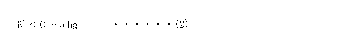

式(1)は以下のように導出される。
Equation (1) is derived as follows.
まず、被剥離基板Cから剥離基板Aを剥離する工程を考える。このとき、剥離基板Aが破損しない条件は式(4)で表わすことができる。ここで、式(4)におけるσmaxは剥離基板Aの限界曲げ応力、σbendは剥離基板Aを曲げた時に剥離基板Aに係る引張り方向の応力、σbondは被剥離基板Cの粘着層Bからかかる引張り応力である。σbendは剥離基板Aの二次モーメントから算出することができ、式(5)で表わすことができる。ここで式(5)におけるLは剥離基板Aの剥離方向の長さ、hは剥離基板Aの厚み、xは剥離基板Aの変化量、Eは剥離基板Aのヤング率である。σbendは力学的な力の分解により、式(6)で表わされる。特に、本発明のような剥離角が小さい場合には、剥離時の力は面密着力にて近似することができる。ここで、式(6)におけるAは剥離基板Aと被剥離基板Cとの面密着力、θは曲げ角度である。式(5)および式(6)を式(4)に代入すると、式(7)となる。この式(7)より、剥離基板Aと被剥離基板Cとの面密着力Aの項に着目し、整理すると式(8)のように表される。曲げ角度θを剥離基板Aの剥離方向の長さLと剥離基板Aの変化量xで表わすと、式(9)のように表される。式(9)を式(8)に代入することにより、上記式(1)が導出される。なお、式(1)におけるx以外の変数は材料の特性であり、決まった値を有している。また、xも限界変形量xmaxによって制限されるため、許容される剥離基板Aと被剥離基板Cとの面密着力は自動的に決定される。
First, consider a process of peeling the release substrate A from the substrate C to be peeled. At this time, the condition that the release substrate A is not damaged can be expressed by the following equation (4). Here, σ max in Equation (4) is the critical bending stress of the release substrate A, σ bend is the tensile stress applied to the release substrate A when the release substrate A is bent, and σ bond is the adhesive layer B of the release substrate C. This is the tensile stress applied. σ bend can be calculated from the second moment of the release substrate A, and can be expressed by Equation (5). Here, L in Formula (5) is the length of the peeling substrate A in the peeling direction, h is the thickness of the peeling substrate A, x is the amount of change of the peeling substrate A, and E is the Young's modulus of the peeling substrate A. σ bend is expressed by Equation (6) by the decomposition of mechanical force. In particular, when the peeling angle is small as in the present invention, the force at the time of peeling can be approximated by the surface adhesion force. Here, A in Formula (6) is a surface adhesion force between the peeling substrate A and the substrate to be peeled C, and θ is a bending angle. When Expression (5) and Expression (6) are substituted into Expression (4), Expression (7) is obtained. From this equation (7), attention is paid to the term of the surface adhesion force A between the peeling substrate A and the substrate C to be peeled, and this is expressed as the following equation (8). When the bending angle θ is expressed by the length L of the peeling substrate A in the peeling direction and the change amount x of the peeling substrate A, the bending angle θ is expressed by the following equation (9). By substituting equation (9) into equation (8), the above equation (1) is derived. It should be noted that variables other than x in Equation (1) are material characteristics and have a fixed value. Further, since x is also limited by the limit deformation amount x max , the allowable surface adhesion force between the peeling substrate A and the substrate to be peeled C is automatically determined.

式(2)および式(3)は以下のように導出される。
Equations (2) and (3) are derived as follows.
剥離開始時、剥離基板Aには図3に示したような力(剥離時の剥離開始部の剥離基板A-被剥離基板Cの粘着力(B’)、剥離時の剥離基板Aに対する基板吸着(保持)力(C)、剥離基板Aの重さ(ρhg))がかかる。これらの関係から、剥離開始時に正常に剥離される条件としては上記式(2)が得られる。ここで、基板吸着(保持)力、即ち、剥離時における垂直方向(Z軸方向)への剥離力Cは真空での保持の場合には小さい値となり、剥離基板A-被剥離基板C間の粘着力に大幅な制限がなされる。この条件を元に、剥離開始部に必要な条件を計算すると、剥離開始部の長さlは図3のような関係が表わされる。図3では、図中の基板端からlの長さにおいては少なくとも式(2)を満たさねばならない。ここで、rは曲率半径、dは許容基板突起および反り量、zは剥離基板Aの端から曲率円の中心方向に伸ばし、反った状態の剥離基板Aと交わる距離である。ここで、lが何によって決定されるか解析すると、まず、三角形の比として式(10)が得られ、この式(10)を整理すると式(11)が得られる。ここで、三角形の三平方の定理を考えると、図3におけるr,z,lは式(12)のように表わされる。この式(12)をlについて整理すると共に、zに式(11)を代入すると、上記式(3)が導出される。このように、剥離開始時に必要な長さlは、曲率半径rと許容基板突起および反り量dとによって定義することができる。なお、曲率半径は剥離基板Aを剥離する装置の仕様や剥離基板Aの物性値によって決定される。また、許容基板突起および反り量dも設備の仕様や剥離基板Aの物性によって規定される。即ち、吸着力が十分な状態で剥離基板Aが正常に剥離される条件は、剥離開始部の剥離基板A-被剥離基板Cとの粘着力B’と、剥離開始部の長さlによって規定される。
At the start of peeling, the peeling substrate A has the force shown in FIG. 3 (the peeling substrate A at the peeling starting portion at the time of peeling-the adhesive force (B ') of the substrate C to be peeled, the substrate adsorption to the peeling substrate A at the time of peeling. (Holding) force (C) and the weight (ρhg) of the release substrate A are applied. From these relationships, the above formula (2) is obtained as a condition for normal peeling at the start of peeling. Here, the substrate adsorption (holding) force, that is, the peeling force C in the vertical direction (Z-axis direction) at the time of peeling becomes a small value in the case of holding in a vacuum, and between the peeling substrate A and the peeling substrate C. Significant restrictions on adhesive strength. Based on this condition, when the conditions necessary for the peeling start portion are calculated, the length l of the peeling start portion represents a relationship as shown in FIG. In FIG. 3, at least a length of 1 from the substrate end in the drawing must satisfy the formula (2). Here, r is a radius of curvature, d is an allowable substrate protrusion and a warp amount, and z is a distance extending from the end of the release substrate A toward the center of the curvature circle and intersecting with the release substrate A in a warped state. Here, when analyzing what is determined by l, first, the expression (10) is obtained as the ratio of the triangles, and the expression (11) is obtained by rearranging the expression (10). Here, when considering the triangular theorem of triangles, r, z, and l in FIG. 3 are expressed as in Expression (12). When this formula (12) is arranged for l and the formula (11) is substituted for z, the above formula (3) is derived. Thus, the length 1 required at the start of peeling can be defined by the radius of curvature r, the allowable substrate protrusion, and the warpage amount d. The radius of curvature is determined by the specifications of the apparatus for peeling the release substrate A and the physical properties of the release substrate A. Further, the allowable substrate protrusion and the warpage amount d are also defined by the specifications of the equipment and the physical properties of the release substrate A. That is, the conditions under which the peeling substrate A is normally peeled with a sufficient adsorbing force are defined by the adhesive strength B ′ between the peeling substrate A and the substrate C to be peeled at the peeling start portion and the length l of the peeling start portion. Is done.
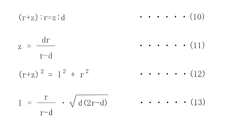
(表示装置)
図4は、図1における可撓性デバイス10の一例としての表示装置(表示装置10A)の断面構成を表したものである。この表示装置10Aは、例えばフレキシブルな極薄型の有機発光カラーディスプレイであり、可撓性を有する駆動基板131と対向基板231との間にTFT層141および表示層142からなる機能層140(例えば、図8参照)が設けられている。本実施の形態では、駆動基板131は支持基板11上に固定されており、駆動基板131上には、TFT層141と表示層142を構成する下部電極142A,有機層142B,上部電極142Cおよび保護膜142D等からなる表示体が設けられる(機能層140A)。対向基板231は支持基板21上に固定されており、対向基板231上には、表示層142を構成するカラーフィルタ142Gおよび封止膜142Eが設けられる(機能層140B)。これら機能層140Aと機能層140Bとを対向させ、封止膜142Eを介してカラーフィルタ層142Gと保護膜142Dとを貼り合わせたのち、支持基板11および支持基板21を剥離することによって表示装置10Aは製造されている。なお、図4は、表示装置10Aの構造を模式的に表わしたものであり、実際の寸法および形状とは異なる場合がある。 (Display device)
FIG. 4 illustrates a cross-sectional configuration of a display device (display device 10A) as an example of the flexible device 10 in FIG. The display device 10A is, for example, a flexible ultra-thin organic light emitting color display, and a functional layer 140 (for example, a TFT layer 141 and a display layer 142 between a flexible driving substrate 131 and a counter substrate 231). 8) is provided. In the present embodiment, the drive substrate 131 is fixed on the support substrate 11, and on the drive substrate 131, the lower electrode 142A, the organic layer 142B, the upper electrode 142C, and the protective layer that constitute the TFT layer 141 and the display layer 142 are provided. A display body made of the film 142D or the like is provided (functional layer 140A). The counter substrate 231 is fixed on the support substrate 21, and a color filter 142G and a sealing film 142E constituting the display layer 142 are provided on the counter substrate 231 (functional layer 140B). The functional layer 140A and the functional layer 140B are opposed to each other, and the color filter layer 142G and the protective film 142D are bonded to each other through the sealing film 142E. Is manufactured. FIG. 4 schematically shows the structure of the display device 10A and may differ from the actual size and shape.
図4は、図1における可撓性デバイス10の一例としての表示装置(表示装置10A)の断面構成を表したものである。この表示装置10Aは、例えばフレキシブルな極薄型の有機発光カラーディスプレイであり、可撓性を有する駆動基板131と対向基板231との間にTFT層141および表示層142からなる機能層140(例えば、図8参照)が設けられている。本実施の形態では、駆動基板131は支持基板11上に固定されており、駆動基板131上には、TFT層141と表示層142を構成する下部電極142A,有機層142B,上部電極142Cおよび保護膜142D等からなる表示体が設けられる(機能層140A)。対向基板231は支持基板21上に固定されており、対向基板231上には、表示層142を構成するカラーフィルタ142Gおよび封止膜142Eが設けられる(機能層140B)。これら機能層140Aと機能層140Bとを対向させ、封止膜142Eを介してカラーフィルタ層142Gと保護膜142Dとを貼り合わせたのち、支持基板11および支持基板21を剥離することによって表示装置10Aは製造されている。なお、図4は、表示装置10Aの構造を模式的に表わしたものであり、実際の寸法および形状とは異なる場合がある。 (Display device)
FIG. 4 illustrates a cross-sectional configuration of a display device (
(表示装置10Aの全体構成)
図5は、表示装置10Aの全体構成を表すものである。表示装置10Aは、駆動基板131上の中央部に表示領域310を有しており、表示領域310の周辺には、例えば映像表示用のドライバである信号線駆動回路320および走査線駆動回路330が設けられている。 (Overall configuration ofdisplay device 10A)
FIG. 5 illustrates the overall configuration of thedisplay device 10A. The display device 10A has a display area 310 at the center on the drive substrate 131. Around the display area 310, for example, a signal line drive circuit 320 and a scanning line drive circuit 330, which are drivers for displaying images, are provided. Is provided.
図5は、表示装置10Aの全体構成を表すものである。表示装置10Aは、駆動基板131上の中央部に表示領域310を有しており、表示領域310の周辺には、例えば映像表示用のドライバである信号線駆動回路320および走査線駆動回路330が設けられている。 (Overall configuration of
FIG. 5 illustrates the overall configuration of the
表示領域310には、マトリクス状に二次元配置された複数の画素40R,40G,40Bと、それらを駆動するための画素駆動回路340とが形成されている。画素駆動回路340において、列方向には複数の信号線320Aが配置され、行方向には複数の走査線330Aが配置されている。各信号線320Aと各走査線330Aとの各交差点に、画素40R,40G,40Bが対応して設けられている。画素40R,40G,40Bはそれぞれ、赤色,緑色,青色を発光する画素である。各信号線320Aは信号線駆動回路320に、各走査線330Aは走査線駆動回路330にそれぞれ接続されている。
In the display area 310, a plurality of pixels 40R, 40G, and 40B that are two-dimensionally arranged in a matrix and a pixel driving circuit 340 for driving them are formed. In the pixel driving circuit 340, a plurality of signal lines 320A are arranged in the column direction, and a plurality of scanning lines 330A are arranged in the row direction. Pixels 40R, 40G, and 40B are provided corresponding to each intersection of each signal line 320A and each scanning line 330A. The pixels 40R, 40G, and 40B are pixels that emit red, green, and blue, respectively. Each signal line 320A is connected to the signal line driving circuit 320, and each scanning line 330A is connected to the scanning line driving circuit 330.
信号線駆動回路320は、信号供給源(図示せず)から供給される輝度情報に応じた映像信号の信号電圧を、信号線320Aを介して選択された画素40R,40G,40Bに供給するものである。信号線320Aには信号線駆動回路320からの信号電圧が印加される。
The signal line driving circuit 320 supplies a signal voltage of a video signal corresponding to luminance information supplied from a signal supply source (not shown) to the selected pixels 40R, 40G, and 40B via the signal line 320A. It is. A signal voltage from the signal line driver circuit 320 is applied to the signal line 320A.
走査線駆動回路330は、入力されるクロックパルスに同期してスタートパルスを順にシフト(転送)するシフトレジスタ等によって構成されている。走査線駆動回路330は、画素40R,40G,40Bへの映像信号の書き込みに際し行単位でそれらを走査し、各走査線330Aに走査信号を順次供給するものである。走査線330Aには、走査線駆動回路330からの走査信号が供給される。
The scanning line driving circuit 330 includes a shift register or the like that sequentially shifts (transfers) the start pulse in synchronization with the input clock pulse. The scanning line driving circuit 330 scans them in units of rows when writing video signals to the pixels 40R, 40G, and 40B, and sequentially supplies the scanning signals to the respective scanning lines 330A. A scanning signal from the scanning line driving circuit 330 is supplied to the scanning line 330A.
画素駆動回路340は、TFT層141に設けられている。この画素駆動回路340は、図6に示したように、駆動トランジスタTr1および書込トランジスタTr2と、その間の保持容量30Cと、有機発光素子ELとを有するアクティブ型の駆動回路である。
The pixel drive circuit 340 is provided in the TFT layer 141. As shown in FIG. 6, the pixel driving circuit 340 is an active driving circuit having a driving transistor Tr1 and a writing transistor Tr2, a storage capacitor 30C therebetween, and an organic light emitting element EL.
表示装置10Aの各層は、例えば以下のような構成をとる。なお、駆動基板131および対向基板231は上記可撓性基板13および可撓性基板23であり、同様の構成を有する。
Each layer of the display device 10A has the following configuration, for example. The driving substrate 131 and the counter substrate 231 are the flexible substrate 13 and the flexible substrate 23, and have the same configuration.
TFT層141には、具体的には、例えばゲート電極141A,ゲート絶縁膜141B,チャネル層としての半導体層141Cおよびソース・ドレイン電極141D(141D1,141D2)により構成されたTFT等が設けられている。これらはCVD(Chemical Vapor Deposition;化学気相成長)法等による成膜およびエッチングの工程を経ることにより形成する。ソース・ドレイン電極141D(141D1,141D2)は、例えばポリイミド等の絶縁性樹脂材料からなる平坦化層141Eに覆われている。ここで、TFTは無機半導体層を用いた無機TFTあるいは有機半導体層を用いた有機TFTのどちらであってもよい。TFTは画素を選択するためのスイッチング素子としての機能を有する。なお、TFT層141はTFTに限らず、その他の電子デバイス、例えば3D表示用光学デバイスやタッチパネル、モスアイ等の光学機能層、あるいはMEMSデバイスを形成してもよい。
Specifically, the TFT layer 141 is provided with, for example, a TFT composed of a gate electrode 141A, a gate insulating film 141B, a semiconductor layer 141C as a channel layer, and source / drain electrodes 141D (141D1, 141D2). . These are formed through a film forming and etching process by a CVD (Chemical Vapor Deposition) method or the like. The source / drain electrodes 141D (141D1, 141D2) are covered with a planarization layer 141E made of an insulating resin material such as polyimide. Here, the TFT may be either an inorganic TFT using an inorganic semiconductor layer or an organic TFT using an organic semiconductor layer. The TFT has a function as a switching element for selecting a pixel. The TFT layer 141 is not limited to the TFT, and other electronic devices such as an optical functional layer such as a 3D display optical device, a touch panel, and a moth eye, or a MEMS device may be formed.
表示層142は、駆動基板131(平坦化層141E)の側から、アノード電極としての下部電極142A、発光層を含む有機層142Bおよびカソード電極としての上部電極142Cを有している。表示層142では、この上部電極142Cを保護膜142Dが覆い、保護膜142D上に封止膜142Eを間にして、カラーフィルタ142Gを有する対向基板230が設けられている。有機層142Bは下部電極142A側から例えば正孔注入層、正孔輸送層、発光層および電子輸送層をこの順に有している。この発光層は画素40R,40G,40B毎に設けられたものでもよく、各画素40R,40G,40Bに共通して設けられていてもよい。発光層以外の層は、必要に応じて設ければよい。保護膜142Dは、例えば、有機層142Bへの水分の浸入を防止するためのものであり、例えば、酸化アルミニウム(Al2O3),酸化ケイ素(SiO),窒化ケイ素(SiN)あるいは、酸窒化ケイ素(SiON)等の絶縁材料によって形成されている。なお、画素40R,40G,40Bは、それぞれ画素分離膜142Fによって分離され、画素40R,40G,40Bの画素領域P(発光領域)は画素分離膜142Fにより画定されている。また、ここでは、有機層142Bを画素毎に設けた例を示したが、これに限らず、例えば発光領域Pあるいは駆動基板131の全面にベタ膜として形成してもよい。
The display layer 142 includes, from the drive substrate 131 (planarization layer 141E) side, a lower electrode 142A as an anode electrode, an organic layer 142B including a light emitting layer, and an upper electrode 142C as a cathode electrode. In the display layer 142, the upper electrode 142C is covered with a protective film 142D, and the counter substrate 230 including the color filter 142G is provided on the protective film 142D with the sealing film 142E interposed therebetween. The organic layer 142B has, for example, a hole injection layer, a hole transport layer, a light emitting layer, and an electron transport layer in this order from the lower electrode 142A side. This light emitting layer may be provided for each of the pixels 40R, 40G, and 40B, or may be provided in common for each of the pixels 40R, 40G, and 40B. Layers other than the light emitting layer may be provided as necessary. The protective film 142D is for preventing moisture from entering the organic layer 142B, for example, aluminum oxide (Al 2 O 3 ), silicon oxide (SiO), silicon nitride (SiN), or oxynitride It is formed of an insulating material such as silicon (SiON). The pixels 40R, 40G, and 40B are separated by a pixel separation film 142F, and the pixel region P (light emitting region) of the pixels 40R, 40G, and 40B is defined by the pixel separation film 142F. Although an example in which the organic layer 142B is provided for each pixel has been described here, the present invention is not limited to this. For example, the organic layer 142B may be formed as a solid film on the entire surface of the light emitting region P or the driving substrate 131.
カラーフィルタ層142Gは、例えば画素40R,40G,40Bに対応するカラーフィルタおよびカラーフィルタの間のブラックマトリクスを有している(図示せず)。このカラーフィルタ層142Gは、上記のように対向基板231側に設けられており、封止膜142Eを介して表示層142と貼り合わされている。封止膜142Eは、例えば、上記保護膜142Dで用いた材料、あるいは、紫外線(UV)硬化樹脂あるいは熱硬化樹脂等により構成されている。
The color filter layer 142G has, for example, a color filter corresponding to the pixels 40R, 40G, and 40B and a black matrix between the color filters (not shown). The color filter layer 142G is provided on the counter substrate 231 side as described above, and is bonded to the display layer 142 through the sealing film 142E. The sealing film 142E is made of, for example, a material used for the protective film 142D, an ultraviolet (UV) curable resin, a thermosetting resin, or the like.
(表示装置10Aの製造方法)
このような表示装置10Aは、例えば次のように製造することができる。 (Manufacturing method ofdisplay device 10A)
Such adisplay device 10A can be manufactured as follows, for example.
このような表示装置10Aは、例えば次のように製造することができる。 (Manufacturing method of
Such a
まず、図7Aに示したように、例えばガラスからなる支持基板11に、粘着力が上記式(1)および/または式(2),(3)を満たす粘着剤を塗布して粘着層12を形成する。続いて図7Bに示したように、粘着層12上に可撓性を有する駆動基板131を固定したのち、例えば、120~250℃,10~60分にて加熱処理をする。この加熱処理により、駆動基板131の熱収縮を強制的に誘発し、その後の工程における駆動基板131の挙動が安定化する。また、粘着層12を構成する粘着剤の粘着力も安定化する。
First, as shown in FIG. 7A, a pressure-sensitive adhesive layer 12 is formed by applying a pressure-sensitive adhesive satisfying the above formula (1) and / or formulas (2) and (3) to a support substrate 11 made of glass, for example. Form. Subsequently, as shown in FIG. 7B, a flexible drive substrate 131 is fixed on the adhesive layer 12, and then heat treatment is performed at 120 to 250 ° C. for 10 to 60 minutes, for example. By this heat treatment, thermal contraction of the drive substrate 131 is forcibly induced, and the behavior of the drive substrate 131 in the subsequent process is stabilized. Moreover, the adhesive force of the adhesive which comprises the adhesion layer 12 is also stabilized.
続いて、図7Cに示したように、駆動基板131上にTFT層141および表示層142の一部(下部電極142A,有機層142B,上部電極142C,保護膜142Dおよび画素分離膜142F)からなる機能層140Aをこの順に積層する。また、同様の工程を経て、例えばガラスからなる支持基板21上に粘着剤を介して対向基板231およびカラーフィルタ層142Gを含む機能層140Bを形成し、機能層140Aおよび機能層140Bをそれぞれ備えた支持基板11および支持基板21を対向配置する。なお、対向基板21側の粘着層22を構成する粘着剤は、上記式(1)および/または式(2),(3)を満たしてもよいし、満たさなくてもよい。
Subsequently, as shown in FIG. 7C, the TFT substrate 141 and a part of the display layer 142 (the lower electrode 142A, the organic layer 142B, the upper electrode 142C, the protective film 142D, and the pixel separation film 142F) are formed on the driving substrate 131. The functional layer 140A is laminated in this order. Further, through the same process, the functional layer 140B including the counter substrate 231 and the color filter layer 142G is formed on the support substrate 21 made of, for example, glass via an adhesive, and the functional layer 140A and the functional layer 140B are provided. The support substrate 11 and the support substrate 21 are arranged to face each other. In addition, the adhesive which comprises the adhesion layer 22 by the side of the opposing substrate 21 may satisfy | fill the said Formula (1) and / or Formula (2), (3), and does not need to satisfy | fill.
次いで、図8Aに示したように、封止膜142Eおよびシール剤(図示せず)を間に支持基板11および支持基板21を貼り合わせ、可撓性デバイス10である表示装置10Aを含む積層体を形成する。続いて、図8Bに示したように、例えば、剥離開始部にピッキングテープAを貼り付け、矢印方向への引くことにより支持基板11を剥離する。あるいは、曲率のついた真空ステージを回転移動させることによって剥離してもよい。なお、剥離の方法はこれらに限らず他の方法を用いてもよく、さらに粘着ステージや静電気力等の種類を問わない。次いで、同様にして支持基板21を剥離する。これにより、図8Cに示したような表示装置10Aが完成する。
Next, as illustrated in FIG. 8A, the support substrate 11 and the support substrate 21 are bonded to each other with the sealing film 142 </ b> E and a sealant (not illustrated), and the laminate including the display device 10 </ b> A that is the flexible device 10. Form. Subsequently, as shown in FIG. 8B, for example, the picking tape A is attached to the peeling start portion, and the support substrate 11 is peeled by pulling in the arrow direction. Or you may peel by rotating the vacuum stage with a curvature. Note that the peeling method is not limited to these, and other methods may be used, and any type of adhesive stage or electrostatic force may be used. Next, the support substrate 21 is peeled in the same manner. Thereby, the display device 10A as shown in FIG. 8C is completed.
この表示装置10Aでは、各々の画素40R,40G,40Bに対して走査線駆動回路330から書き込みトランジスタTr2のゲート電極141Aを介して走査信号が供給されると共に、信号線駆動回路320から画像信号が書き込みトランジスタTr2を介して保持容量30Cに保持される。即ち、この保持容量30Cに保持された信号に応じて駆動トランジスタTr1がオンオフ制御され、これにより、画素40R,40G,40Bに駆動電流が注入され、正孔と電子とが再結合して発光が起こる。この光は、上部電極142C、保護膜142D、封止膜142Eおよび対向基板230を透過して取り出される。
In the display device 10A, a scanning signal is supplied from the scanning line driving circuit 330 to the respective pixels 40R, 40G, and 40B via the gate electrode 141A of the writing transistor Tr2, and an image signal is received from the signal line driving circuit 320. It is held in the holding capacitor 30C via the write transistor Tr2. That is, the driving transistor Tr1 is controlled to be turned on / off according to the signal held in the holding capacitor 30C, whereby a driving current is injected into the pixels 40R, 40G, and 40B, and holes and electrons are recombined to emit light. Occur. This light passes through the upper electrode 142C, the protective film 142D, the sealing film 142E, and the counter substrate 230 and is extracted.
このような積層体および積層体の剥離方法ならびに可撓性デバイスの製造方法では、可撓性デバイス10である表示装置10Aを構成する駆動基板131および対向基板231をそれぞれ支持基板11および支持基板21に固着する粘着層12および粘着層22のうち、少なくとも、先に剥離する側の粘着層(例えば、粘着層12)を上記式(1)および/または式(2),(3)を満たす粘着力を有する粘着剤を用いて形成する。これにより支持基板11を破損することなく、また、機能層140に負荷をかけることなく剥離することが可能となる。
In such a laminate, a method for peeling the laminate, and a method for manufacturing a flexible device, the driving substrate 131 and the counter substrate 231 that constitute the display device 10A that is the flexible device 10 are used as the supporting substrate 11 and the supporting substrate 21, respectively. Among the pressure-sensitive adhesive layer 12 and the pressure-sensitive adhesive layer 22 that adheres to each other, at least the pressure-sensitive adhesive layer that peels first (for example, the pressure-sensitive adhesive layer 12) satisfies the above formula (1) and / or formulas (2) and (3). It is formed using a pressure-sensitive adhesive. This makes it possible to peel the support substrate 11 without damaging it and without applying a load to the functional layer 140.
一般的に、可撓性基板上に表示素子等の各種デバイスを形成する、所謂フレキシブルディスプレイ等の可撓性デバイスは、可撓性基板をガラス等の剛性を有する基板に固定したのちは既存の表示装置の製造ラインを用いることができるため低コストで製造することができる。しかしながら、ガラス-ガラスのように、剛性を有する基板(例えば、ガラス基板)によって挟持されたデバイスからガラス基板を剥離することは難しく、例えば剥離途中でガラス基板が破損して剥離できなくなる場合があった。あるいは、剥離開始時におけるガラス基板の吸着力が足りず、剥離させることができないという問題があった。
Generally, a flexible device such as a so-called flexible display in which various devices such as display elements are formed on a flexible substrate is an existing one after fixing the flexible substrate to a rigid substrate such as glass. Since a display device manufacturing line can be used, the display device can be manufactured at low cost. However, it is difficult to peel off a glass substrate from a device sandwiched by a rigid substrate (for example, a glass substrate), such as glass-glass. For example, the glass substrate may be damaged during peeling, and may not be peeled off. It was. Or there existed a problem that it was not able to be made to peel because the adsorption | suction power of the glass substrate at the time of peeling start was insufficient.
このため、前述したように、ガラス基板上に金属層を設け、この金属層にレーザを照射して剥離する方法や、例えば可撓性基板の外周部にのみ粘着剤を塗布してガラス基板に固定する方法がとられてきたが、レーザの使用によるコストの増加や、レーザ照射による機能層の劣化、あるいは固定力不足による位置ずれ等の問題があった。
For this reason, as described above, a metal layer is provided on a glass substrate and the metal layer is irradiated with a laser to peel off, for example, a pressure-sensitive adhesive is applied only to the outer peripheral portion of a flexible substrate. Although fixing methods have been used, there have been problems such as an increase in cost due to the use of a laser, deterioration of a functional layer due to laser irradiation, or misalignment due to insufficient fixing force.
これに対して本実施の形態では、例えば先に剥離する側の基板(ここでは、駆動基板131(可撓性基板13)と支持基板11)間の粘着層(粘着層12)が、上記式(1)および式(2),(3)の少なくとも一方を満たす粘着力を有するように調製することにより、機械的に支持基板11と駆動基板131(可撓性基板13)とを剥離することが可能となる。
On the other hand, in the present embodiment, for example, the adhesive layer (adhesive layer 12) between the substrates to be peeled first (here, the drive substrate 131 (flexible substrate 13) and the support substrate 11) is the above formula. The support substrate 11 and the drive substrate 131 (flexible substrate 13) are mechanically peeled off by preparing to have an adhesive force satisfying at least one of (1) and formulas (2) and (3). Is possible.
以上のように、本実施の形態における積層体および積層体の剥離方法ならびに可撓性デバイスの製造方法によれば、支持基板11と駆動基板131(可撓性基板13)との間に、粘着力が上記式(1)および式(2),(3)の少なくとも一方を満たす粘着層12を形成するようにした。これにより、機械的に支持基板11と駆動基板131(可撓性基板13)を、支持基板11の破損や、駆動基板131側に設けられた機能層140に負荷をかけることなく、容易且つ安価に剥離させることが可能となる。
As described above, according to the laminate, the method for peeling the laminate, and the method for manufacturing a flexible device according to the present embodiment, an adhesive is provided between the support substrate 11 and the drive substrate 131 (flexible substrate 13). The pressure-sensitive adhesive layer 12 satisfying at least one of the above formulas (1), (2), and (3) was formed. Thereby, the support substrate 11 and the drive substrate 131 (flexible substrate 13) can be mechanically easily and inexpensively without damaging the support substrate 11 or applying a load to the functional layer 140 provided on the drive substrate 131 side. Can be peeled off.
また、レーザ照射等の処理を行わずに剥離することができるため、支持基板11上でTFT層141および表示層142等が劣化するのを防ぐことができる。更に、支持基板11と駆動基板131との全面に粘着層12を塗布し固着することができるため、高精細な表示装置を製造することが可能となる。
In addition, since the separation can be performed without performing treatment such as laser irradiation, it is possible to prevent the TFT layer 141, the display layer 142, and the like from deteriorating on the support substrate 11. Furthermore, since the adhesive layer 12 can be applied and fixed to the entire surface of the support substrate 11 and the drive substrate 131, a high-definition display device can be manufactured.
以下、上記実施の形態の変形例(変形例1,2)について説明するが、以降の説明において上記実施の形態と同一構成部分については同一符号を付してその説明は適宜省略する。
Hereinafter, modified examples (modified examples 1 and 2) of the above embodiment will be described. In the following description, the same components as those of the above embodiment are denoted by the same reference numerals, and the description thereof will be omitted as appropriate.
<2.変形例>
(変形例1)
図9A~図9Cは、上記実施の形態で説明した表示装置10Aの製造方法の他の例(変形例1)を表したものである。この方法では、例えば上記式(1)および/または式(2),(3)を満たすように調整された粘着層(例えば粘着層12)と可撓性基板13との間に、より粘着力の弱い離型層15が形成される。変形例1ではこの点を除き、上記実施の形態と同様にして表示装置10Aを製造する。 <2. Modification>
(Modification 1)
9A to 9C show another example (modification example 1) of the method for manufacturing thedisplay device 10A described in the above embodiment. In this method, for example, the adhesive force between the pressure-sensitive adhesive layer (for example, the pressure-sensitive adhesive layer 12) adjusted so as to satisfy the above formula (1) and / or the formulas (2) and (3) and the flexible substrate 13 is further increased. Weak release layer 15 is formed. In Modification 1, except for this point, the display device 10A is manufactured in the same manner as in the above embodiment.
(変形例1)
図9A~図9Cは、上記実施の形態で説明した表示装置10Aの製造方法の他の例(変形例1)を表したものである。この方法では、例えば上記式(1)および/または式(2),(3)を満たすように調整された粘着層(例えば粘着層12)と可撓性基板13との間に、より粘着力の弱い離型層15が形成される。変形例1ではこの点を除き、上記実施の形態と同様にして表示装置10Aを製造する。 <2. Modification>
(Modification 1)
9A to 9C show another example (modification example 1) of the method for manufacturing the
離型層15は、粘着層12と可撓性基板13との粘着力を低減するものであり、例えば無機材料によって構成されている。具体的には、窒化シリコン(SiNx),酸化シリコン(SiO2)等が挙げられる。離型層15の厚みは、例えば50nm以上500nm以下であることが好ましい。離型層15は、剥離工程において可撓性基板13側に付着する虞があり、例えば光射出方向の可撓性基板側に設ける場合には膜厚が厚すぎると透過率が低下し、有機ELの発光光を遮ることとなり発光効率が低下するため、薄いほうが好ましい。
The release layer 15 reduces the adhesive force between the adhesive layer 12 and the flexible substrate 13 and is made of, for example, an inorganic material. Specific examples include silicon nitride (SiN x ) and silicon oxide (SiO 2 ). The thickness of the release layer 15 is preferably 50 nm or more and 500 nm or less, for example. The release layer 15 may adhere to the flexible substrate 13 side in the peeling step. For example, when the release layer 15 is provided on the flexible substrate side in the light emitting direction, if the film thickness is too thick, the transmittance decreases, and the organic layer A thinner one is preferable because it blocks light emitted from the EL and lowers the light emission efficiency.
本変形例の表示装置10Aは以下のように製造される。
The display device 10A according to this modification is manufactured as follows.
まず、図9Aに示したように、駆動基板131上に、例えばCVD法を用いて、例えばSiN膜を成膜して離型層15を形成する。また、上記実施の形態と同様に、支持基板11上に上記式(1)および/または式(2),(3)を満たす粘着剤を塗布して粘着層12を形成する。続いて、図9Bに示したように、対向配置した粘着層12と離型層15とを貼り合わせる。以降、実施の形態と同様に、駆動基板131上に機能層14を形成したのち、別途支持基板21上に粘着層22を介して固着した対向基板231を貼り合わせることにより、図9Cに示したように可撓性デバイス10である表示装置10Aを含む積層体を形成する。
First, as shown in FIG. 9A, a release layer 15 is formed on the drive substrate 131 by using, for example, a CVD method to form, for example, a SiN film. Similarly to the above embodiment, an adhesive that satisfies the above formula (1) and / or formulas (2) and (3) is applied on the support substrate 11 to form the adhesive layer 12. Subsequently, as shown in FIG. 9B, the adhesive layer 12 and the release layer 15 that are arranged to face each other are bonded together. Thereafter, as in the embodiment, after the functional layer 14 is formed on the drive substrate 131, the counter substrate 231 fixed to the support substrate 21 via the adhesive layer 22 is bonded to the support substrate 21 as shown in FIG. 9C. Thus, a laminated body including the display device 10A which is the flexible device 10 is formed.
この後、上記実施の形態と同様の方法を用いて、支持基板11および支持基板21を剥離することにより、表示装置10Aが完成する。
Thereafter, the support substrate 11 and the support substrate 21 are peeled off by using the same method as in the above embodiment, whereby the display device 10A is completed.
以上のように、本変形例では、上記式(1)および/または式(2),(3)を満たすように調整された粘着層12と駆動基板131との間に、より粘着力の弱い離型層15を形成することにより、駆動基板131と粘着層12との粘着量が低減され、より弱い力で支持基板11を剥離することが可能となる。即ち、剥離時に、例えば表示層142等の機能層140への負荷による特性の劣化が抑えられ、信頼性の高い可撓性デバイスを提供することが可能となる。
As described above, in this modification, the adhesive force between the adhesive layer 12 adjusted to satisfy the above formula (1) and / or the formulas (2) and (3) and the drive substrate 131 is weaker. By forming the release layer 15, the amount of adhesion between the drive substrate 131 and the adhesive layer 12 is reduced, and the support substrate 11 can be peeled off with a weaker force. That is, at the time of peeling, deterioration of characteristics due to a load on the functional layer 140 such as the display layer 142 is suppressed, and a highly reliable flexible device can be provided.
また、駆動基板131と離型層15との間で剥離されるため、剥離後の駆動基板131側への粘着剤の付着が低減される。よって、表示装置10Aの視認性が向上すると共に、粘着剤の残存によるゴミ等の付着が防止される。
Further, since the separation is performed between the drive substrate 131 and the release layer 15, adhesion of the adhesive to the drive substrate 131 side after the separation is reduced. Therefore, the visibility of the display device 10A is improved and adhesion of dust and the like due to the remaining adhesive is prevented.
なお、本変形例では、離型層15を一方の支持基板11側に設けたが、他方の支持基板21側の両方に設けてもよい。
In this modification, the release layer 15 is provided on the one support substrate 11 side, but may be provided on both the other support substrate 21 side.
(変形例2)
図10A~図10Cは、上記実施の形態および変形例1で説明した表示装置10Aの製造方法の他の例(変形例2)を表したものである。この方法では、例えば支持基板11と上記式(1)および/または式(2),(3)を満たすように調整された粘着層(例えば粘着層12)との間に、より粘着力の弱い離型層15が形成される。変形例2ではこの点を除き、上記実施の形態と同様にして表示装置10Aを製造する。 (Modification 2)
10A to 10C show another example (Modification 2) of the method for manufacturing thedisplay device 10A described in the above embodiment and Modification 1. FIG. In this method, for example, the adhesive force is weaker between the support substrate 11 and the adhesive layer (for example, the adhesive layer 12) adjusted to satisfy the above formula (1) and / or the formulas (2) and (3). A release layer 15 is formed. In Modification 2, except for this point, the display device 10A is manufactured in the same manner as in the above embodiment.
図10A~図10Cは、上記実施の形態および変形例1で説明した表示装置10Aの製造方法の他の例(変形例2)を表したものである。この方法では、例えば支持基板11と上記式(1)および/または式(2),(3)を満たすように調整された粘着層(例えば粘着層12)との間に、より粘着力の弱い離型層15が形成される。変形例2ではこの点を除き、上記実施の形態と同様にして表示装置10Aを製造する。 (Modification 2)
10A to 10C show another example (Modification 2) of the method for manufacturing the
本変形例の表示装置10Aは以下のように製造される。
The display device 10A according to this modification is manufactured as follows.
まず、図10Aに示したように、支持基板11上に、離型層15および粘着層12をこの順に形成する。具体的には、例えばCVD法を用いて、支持基板11上に、例えばSiN膜を成膜して離型層15を形成したのち、離型層15上に、上記式(1)および/または式(2),(3)を満たす粘着剤を塗布して粘着層12を形成する。続いて、図10Bに示したように、粘着層12上に駆動基板131を固着したのち、機能層140Aを形成する。この後、別途支持基板21上に粘着層22を介して固着した対向基板231を貼り合わせることにより、図10Cに示したように可撓性デバイス10である表示装置10Aを含む積層体を形成する。
First, as shown in FIG. 10A, a release layer 15 and an adhesive layer 12 are formed in this order on a support substrate 11. Specifically, for example, a CVD method is used to form a release layer 15 by forming, for example, a SiN film on the support substrate 11, and then the above formula (1) and / or on the release layer 15. The pressure-sensitive adhesive satisfying the formulas (2) and (3) is applied to form the pressure-sensitive adhesive layer 12. Subsequently, as shown in FIG. 10B, after fixing the drive substrate 131 on the adhesive layer 12, the functional layer 140 </ b> A is formed. Thereafter, a counter substrate 231 that is separately fixed on the support substrate 21 via the adhesive layer 22 is bonded to form a laminate including the display device 10A that is the flexible device 10 as shown in FIG. 10C. .
この後、上記実施の形態と同様の方法を用いて、支持基板11および支持基板21を剥離することにより、表示装置10Aが完成する。
Thereafter, the support substrate 11 and the support substrate 21 are peeled off by using the same method as in the above embodiment, whereby the display device 10A is completed.
以上のように、本変形例では、支持基板11と上記式(1)および/または式(2),(3)を満たすように調整された粘着層12との間に、より粘着力の弱い離型層15を形成するようにした。これにより、支持基板11と粘着層12との粘着量が低減され、より弱い力で支持基板11を剥離することが可能となる。即ち、例えば表示層142等の機能層14の損傷を抑え、信頼性の高い可撓性デバイスを提供することが可能となる。
As described above, in this modification, the adhesive force is weaker between the support substrate 11 and the adhesive layer 12 adjusted to satisfy the above formula (1) and / or the formulas (2) and (3). A release layer 15 was formed. Thereby, the adhesion amount of the support substrate 11 and the adhesion layer 12 is reduced, and it becomes possible to peel the support substrate 11 with a weaker force. That is, for example, it is possible to suppress damage to the functional layer 14 such as the display layer 142 and to provide a highly reliable flexible device.
なお、本変形例では、離型層15を一方の支持基板側に設けたが、上記変形例1と同様に他方の支持基板(ここでは、支持基板21)側に設けてもよいし、両方の支持基板11,21と粘着層12,22との間に設けてもよい。
In this modification, the release layer 15 is provided on one support substrate side. However, similarly to the modification 1, the release layer 15 may be provided on the other support substrate (here, the support substrate 21), or both. The support substrates 11 and 21 and the adhesive layers 12 and 22 may be provided.
また、変形例1と変形例2とを組み合わせて表示装置10Aを製造してもよい。例えば、支持基板11側では、支持基板11と粘着層12との間に離型層15を設け、支持基板21側では粘着層22と対向基板231との間に離型層21を形成してもよく、またその逆でもよい。
Further, the display device 10A may be manufactured by combining the first modification and the second modification. For example, the release layer 15 is provided between the support substrate 11 and the adhesive layer 12 on the support substrate 11 side, and the release layer 21 is formed between the adhesive layer 22 and the counter substrate 231 on the support substrate 21 side. Or vice versa.
更に、上記式(1)および/または式(2),(3)を満たす粘着層12の粘着力等の物性は、外部からの刺激(例えば、光,熱,電磁気力等)によって制御してもよい。
Further, the physical properties such as the adhesive strength of the adhesive layer 12 satisfying the above formulas (1) and / or (2) and (3) are controlled by external stimuli (for example, light, heat, electromagnetic force, etc.). Also good.
(変形例3)
図11A~図12Bは、上記実施の形態の変形例3に係る表示装置1の製造工程の一部を表したものである。本変形例では、大型基板上に、例えば表示装置10Aとなる可撓性デバイス10を複数形成し、基板を貼り合わせた後に、個々に分割する工程を説明する。なお、ここでは、表示装置10Aを例に説明する。 (Modification 3)
11A to 12B show a part of the manufacturing process of the display device 1 according to the third modification of the above embodiment. In this modification, for example, a process in which a plurality offlexible devices 10 to be the display device 10A, for example, are formed on a large substrate and the substrates are bonded together and then divided individually will be described. Here, the display device 10A will be described as an example.
図11A~図12Bは、上記実施の形態の変形例3に係る表示装置1の製造工程の一部を表したものである。本変形例では、大型基板上に、例えば表示装置10Aとなる可撓性デバイス10を複数形成し、基板を貼り合わせた後に、個々に分割する工程を説明する。なお、ここでは、表示装置10Aを例に説明する。 (Modification 3)
11A to 12B show a part of the manufacturing process of the display device 1 according to the third modification of the above embodiment. In this modification, for example, a process in which a plurality of
一般に、複数の可撓性デバイスを大型基板上に一括で製造する場合、一方の支持基板に固着された可撓性基板(例えば、対向基板)上に機能層(例えば、カラーフィルタおよび封止膜)を形成したのち、機能層ごと可撓性基板に切り込みを入れ、他方の支持基板に固着された可撓性基板(例えば、発光層を含む有機膜等が形成された駆動基板)を貼り合わせる。この後、支持基板をそれぞれ剥離すると共に、切り込みに沿って分割することで、複数の可撓性デバイスを一括で製造することができる。
In general, when a plurality of flexible devices are collectively manufactured on a large substrate, a functional layer (for example, a color filter and a sealing film) is formed on a flexible substrate (for example, a counter substrate) fixed to one support substrate. ), And a functional substrate is cut into the flexible substrate, and a flexible substrate (for example, a driving substrate on which an organic film including a light-emitting layer is formed) fixed to the other supporting substrate is bonded. . Thereafter, the support substrates are respectively peeled off and divided along the cuts, whereby a plurality of flexible devices can be manufactured collectively.
しかしながら、機能層を形成した後に切り込みを入れると機能層にクラック等の損傷が生じ、デバイスの信頼性が低下する虞がある。
However, if a cut is made after the functional layer is formed, the functional layer may be damaged, such as cracks, and the reliability of the device may be reduced.
そこで、本変形例では、複数の可撓性デバイス10(表示装置10A)の一括製造を以下のように行う。まず、図11Aに示したように、支持基板21上に粘着層22(ここでは、省略する)を介して固着された大型の対向基板231上に、機能層14として、ここではカラーフィルタ層142Gを複数形成する。続いて、図11Bに示したように、各カラーフィルタ142Gの周縁部に切り込みCLを入れる。次に、図11Cに示したように、カラーフィルタ142G上に封止膜142Eを形成したのち、図12Aに示したように、支持基板11に粘着層12(ここでは、省略する)を介して固着され、別途TFT層141や有機膜142B等が形成された駆動基板131を貼り合わせる。最後に、図12Bに示したように支持基板11および支持基板21をそれぞれ剥離すると共に、複数の可撓性デバイス10を切り込みCLに沿って分割することで、複数の表示装置10Aが製造される。
Therefore, in this modification, a plurality of flexible devices 10 (display device 10A) are collectively manufactured as follows. First, as shown in FIG. 11A, on the large counter substrate 231 fixed on the support substrate 21 via an adhesive layer 22 (not shown here), as the functional layer 14, here the color filter layer 142G. A plurality of are formed. Subsequently, as shown in FIG. 11B, cuts CL are made at the peripheral edge of each color filter 142G. Next, as shown in FIG. 11C, after forming a sealing film 142E on the color filter 142G, as shown in FIG. 12A, the support substrate 11 is provided with an adhesive layer 12 (omitted here). The driving substrate 131, which is fixed and separately formed with the TFT layer 141, the organic film 142B, and the like, is bonded. Finally, as shown in FIG. 12B, the support substrate 11 and the support substrate 21 are peeled off, and the plurality of flexible devices 10 are divided along the cuts CL, whereby a plurality of display devices 10A are manufactured. .
図13は、図12AのI-I線における可撓性デバイス10の断面構成を模式的に表したものである。本変形例の方法を用いることにより、封止膜142Eへの損傷が防がれると共に、カラーフィルタ142Gの端面には封止膜142Eが形成される。なお、ここでは、対向基板231側の製造工程を例に説明したが、駆動基板131側の製造工程にも適用できる。なお、この場合には、例えば、機能層に相当する上部電極142Cまた形成したのち切り込みを入れ、その後、保護膜142Dを形成する。
FIG. 13 schematically shows a cross-sectional configuration of the flexible device 10 taken along the line II in FIG. 12A. By using the method of this modification, damage to the sealing film 142E is prevented, and the sealing film 142E is formed on the end face of the color filter 142G. Here, the manufacturing process on the counter substrate 231 side has been described as an example, but the present invention can also be applied to the manufacturing process on the drive substrate 131 side. In this case, for example, the upper electrode 142C corresponding to the functional layer is formed, and then a cut is made, and then the protective film 142D is formed.
以上のように、本変形例では、支持基板21(あるいは、支持基板11)に固着された対向基板231(あるいは、駆動基板131)上にカラーフィルタ142G(あるいは、有機膜142Bおよび上部電極142C等)を形成したのち、カラーフィルタ142Gおよび対向基板231(あるいは、上部電極142Cから駆動基板131にかけて)に切り込みCLを入れ、この後、カラーフィルタ142(あるいは、有機膜142B等)を保護する封止膜142E(あるいは、保護膜142D)を形成するようにした。これにより、封止膜142E(あるいは、保護膜142D)への損傷が防がれ、製造歩留まりが向上する。また、カラーフィルタ142Gおよび対向基板231(あるいは、有機膜142BやTFT層141等)の端面に、例えば、SiNやAl2O3等の無機材料からなる封止膜142G(あるいは、保護膜142D)が形成されるため、有機材料によって形成された層への水分等の浸入が抑制され、信頼性が向上する。
As described above, in the present modification, the color filter 142G (or the organic film 142B and the upper electrode 142C) are formed on the counter substrate 231 (or the drive substrate 131) fixed to the support substrate 21 (or the support substrate 11). ), A cut CL is made in the color filter 142G and the counter substrate 231 (or from the upper electrode 142C to the drive substrate 131), and then the seal that protects the color filter 142 (or the organic film 142B or the like). A film 142E (or a protective film 142D) is formed. Thereby, damage to the sealing film 142E (or the protective film 142D) is prevented, and the manufacturing yield is improved. Further, a sealing film 142G (or protective film 142D) made of an inorganic material such as SiN or Al 2 O 3 is formed on the end faces of the color filter 142G and the counter substrate 231 (or the organic film 142B, the TFT layer 141, etc.). Therefore, intrusion of moisture or the like into the layer formed of the organic material is suppressed, and the reliability is improved.
なお、ここでは、複数の可撓性デバイス10を一括で製造する場合を例に説明したが、これに限らず、本変形例の製造方法は、一枚の基板から1つの可撓性デバイス10を製造する場合にも適用できる。
Here, the case where a plurality of flexible devices 10 are manufactured collectively has been described as an example. However, the present invention is not limited to this, and the manufacturing method of the present modified example can be applied to a single flexible device 10 from a single substrate. It can also be applied to the manufacture of
<3.適用例>
本実施の形態および変形例1~3の方法を用いて作製された表示装置10Aは、テレビジョン装置,デジタルカメラ,ノート型パーソナルコンピュータ、携帯電話等の携帯端末装置あるいはビデオカメラ等、外部から入力された映像信号あるいは内部で生成した映像信号を、画像あるいは映像として表示するあらゆる分野の電子機器の表示装置に適用することが可能である。 <3. Application example>
Thedisplay device 10A manufactured using the method of the present embodiment and the first to third modifications is input from the outside, such as a television device, a digital camera, a notebook personal computer, a mobile terminal device such as a mobile phone, or a video camera. The present invention can be applied to display devices of electronic devices in various fields that display the generated video signal or the video signal generated inside as an image or video.
本実施の形態および変形例1~3の方法を用いて作製された表示装置10Aは、テレビジョン装置,デジタルカメラ,ノート型パーソナルコンピュータ、携帯電話等の携帯端末装置あるいはビデオカメラ等、外部から入力された映像信号あるいは内部で生成した映像信号を、画像あるいは映像として表示するあらゆる分野の電子機器の表示装置に適用することが可能である。 <3. Application example>
The
(適用例1)
図14A,14Bは、電子ブックの外観構成を表している。この電子ブックは、例えば、表示部110および非表示部120と、操作部130とを備えている。なお、操作部130は、図14Aに示したように非表示部120の前面に設けられていてもよいし、図14Bに示したように上面に設けられていてもよい。表示部110が表示装置1により構成される。なお、表示装置1は、図14A,14Bに示した電子ブックと同様の構成を有するPDA(Personal Digital Assistants)等に搭載されてもよい。 (Application example 1)
14A and 14B show the external configuration of an electronic book. The electronic book includes, for example, adisplay unit 110, a non-display unit 120, and an operation unit 130. Note that the operation unit 130 may be provided on the front surface of the non-display unit 120 as illustrated in FIG. 14A or may be provided on the upper surface as illustrated in FIG. 14B. The display unit 110 is configured by the display device 1. The display device 1 may be mounted on a PDA (Personal Digital Assistants) having the same configuration as the electronic book shown in FIGS. 14A and 14B.
図14A,14Bは、電子ブックの外観構成を表している。この電子ブックは、例えば、表示部110および非表示部120と、操作部130とを備えている。なお、操作部130は、図14Aに示したように非表示部120の前面に設けられていてもよいし、図14Bに示したように上面に設けられていてもよい。表示部110が表示装置1により構成される。なお、表示装置1は、図14A,14Bに示した電子ブックと同様の構成を有するPDA(Personal Digital Assistants)等に搭載されてもよい。 (Application example 1)
14A and 14B show the external configuration of an electronic book. The electronic book includes, for example, a
(適用例2)
図15は、タブレットパーソナルコンピュータの外観を表したものである。このタブレットパーソナルコンピュータは、例えば、タッチパネル部310および筐体320を有しており、タッチパネル部310が上記表示装置1により構成されている。 (Application example 2)
FIG. 15 shows the appearance of a tablet personal computer. The tablet personal computer has, for example, atouch panel unit 310 and a housing 320, and the touch panel unit 310 is configured by the display device 1.
図15は、タブレットパーソナルコンピュータの外観を表したものである。このタブレットパーソナルコンピュータは、例えば、タッチパネル部310および筐体320を有しており、タッチパネル部310が上記表示装置1により構成されている。 (Application example 2)
FIG. 15 shows the appearance of a tablet personal computer. The tablet personal computer has, for example, a
以上、実施の形態および変形例1~3を挙げて本技術を説明したが、本技術は上記実施の形態等に限定されるものではなく、種々の変形が可能である。例えば、上記実施の形態等では、表示装置10AがTFT層141を有する場合、即ち、アクティブマトリクス型の表示装置である場合について説明したが、表示装置10Aはパッシブマトリクス型であってもよい。
Although the present technology has been described with the embodiment and the first to third modifications, the present technology is not limited to the above-described embodiment and the like, and various modifications can be made. For example, in the above-described embodiment and the like, the case where the display device 10A includes the TFT layer 141, that is, the case where the display device is an active matrix display device has been described, but the display device 10A may be a passive matrix type.
更に、上記実施の形態等およびその適用例で説明した各部の材料および厚み、または形成方法および形成条件等は限定されるものではなく、他の材料および厚みとしてもよく、または他の形成方法および形成条件としてもよい。例えば、上記実施の形態等では、粘着層12,22を支持基板11,21の全面に形成した例を示したが、これに限らず所定の形状、例えば、表示装置10Aの所謂表示部および周辺部に粘着剤が存在しないようにパターン形成してもよい。
Furthermore, the materials and thicknesses of the respective parts described in the above embodiments and the application examples thereof and the forming method and forming conditions are not limited, and other materials and thicknesses may be used, or other forming methods and It is good also as formation conditions. For example, in the above-described embodiment and the like, the example in which the adhesive layers 12 and 22 are formed on the entire surfaces of the support substrates 11 and 21 has been described. However, the present invention is not limited to this. The pattern may be formed so that no adhesive is present in the part.
更にまた、上記実施の形態等では、画素として赤色,緑色,青色からなる3種類の画素2R,画素2Gおよび画素2Bを設けた表示装置を例に説明したが、これら3色画素に白色画素あるいは黄色画素を組み合わせてもよい。
Furthermore, in the above-described embodiment and the like, a display device provided with three types of pixels 2R, 2G, and 2B made of red, green, and blue as an example has been described. Yellow pixels may be combined.
また、上記実施の形態等の表示装置10Aは、有機EL素子を備えた表示装置のほか、無機EL素子,液晶素子,電気泳動型の表示素子等、種々の表示素子を備えた表示装置にも適用可能である。
The display device 10A according to the above-described embodiment is not only a display device including an organic EL element but also a display device including various display elements such as an inorganic EL element, a liquid crystal element, and an electrophoretic display element. Applicable.
更に、上記実施の形態等の表示装置10Aは、他の層を含んでいてもよい。例えば、各可撓性基板13,23の表示層142等の機能層14側に離型層15と同様の材料からなる無機膜を形成することにより、この無機膜はバリア層として働き、例えば表示層142を構成する有機膜への水分の侵入を低減することが可能となる。これにより、信頼性を向上させることができる。
Furthermore, the display device 10A according to the above-described embodiment or the like may include other layers. For example, by forming an inorganic film made of the same material as the release layer 15 on the functional layer 14 side such as the display layer 142 of each of the flexible substrates 13 and 23, the inorganic film functions as a barrier layer. It becomes possible to reduce the intrusion of moisture into the organic film constituting the layer 142. Thereby, reliability can be improved.
なお、本明細書中に記載された効果はあくまで例示であって限定されるものではなく、また、他の効果があってもよい。
In addition, the effect described in this specification is an illustration to the last, and is not limited, Moreover, there may exist another effect.
なお、本技術は以下のような構成を取ることも可能である。
(1)
第1基板上に、下記式(1)および式(2),(3)の少なくとも一方を満たす粘着力を有する第1粘着層を形成することと、
前記第1粘着層上に第2基板を固着することと、
前記第2基板上に第1機能層を形成することと、
前記第1基板を前記第2基板から剥離することと
を含む積層体の剥離方法。

(L:第1基板の剥離方向の長さ、h:第1基板の厚み(mm)、x:第1基板の許容変形量、E:第1基板のヤング率、σmax:第1基板の限界曲げ応力)

(B’:剥離時における剥離開始部の第1基板と第2基板との粘着力、C:剥離時における垂直方向(Z軸方向)への剥離力、ρ:第1基板の密度、h:第1基板の厚み(mm)、g:重力定数)

(l:剥離開始領域の幅、d:第1基板突起および反り量、r:重力定数)
(2)
前記第1粘着層は、前記式(1)および式(2),(3)の両方を満たす、前記(1)に記載の多層膜基板の製造方法。
(3)
前記第2基板の前記第1粘着層に固着する面に離型層を形成したのち、前記第1粘着層上に前記第2基板を固着する、前記(1)または(2)に記載の多層膜基板の製造方法。
(4)
前記第1基板上に離型層を形成したのち、前記第1粘着層を形成する、前記(1)または(2)に記載の多層膜基板の製造方法。
(5)
前記離型層は無機材料により形成されている、前記(3)または(4)に記載の多層膜基板の製造方法。
(6)
前記粘着層を介して前記第1基板に固着された前記第2基板上に、前記第1機能層を形成すると共に、前記第1機能層の周縁部に切り込みを入れたのち、前記第1機能層上に保護膜を形成する、前記(1)乃至(5)のうちのいずれかに記載の積層体の剥離方法。
(7)
第3基板上に第2粘着層を介して第4基板を固着することと、
前記第2基板と前記第4基板とを対向配置して貼り合わせることとを含み、
前記第2基板と前記第4基板とを貼り合わせたのち、前記第1基板および前記第3基板をこの順に剥離する、前記(1)乃至(6)のうちのいずれかに記載の多層膜基板の製造方法。
(8)
前記第3基板上に前記第4基板を固着させたのち、前記第4基板上に第2機能層を形成する、前記(7)に記載の多層膜基板の製造方法。
(9)
前記第1機能層および前記第2機能層は半導体層、表示層およびカラーフィルタのうちのいずれかである、前記(8)に記載の多層膜基板の製造方法。
(10)
前記第1基板および前記第3基板は剛性を有する、前記(7)乃至(9)のうちのいずれかに記載の多層膜基板の製造方法。
(11)
前記第2基板および前記第4基板は可撓性を有する、前記(7)乃至(10)のうちのいずれかに記載の多層膜基板の製造方法。
(12)
前記第2粘着層は前記式(1)および式(2),(3)の少なくとも一方を満たす粘着力を有する、前記(3)乃至(11)のうちいずれかに記載の多層膜基板の製造方法。
(13)
第1基板上に、粘着力が下記式(1)および式(2),(3)の少なくとも一方を満たす粘着層を形成することと、
前記粘着層上に可撓性を有する第2基板を固定することと、
前記第2基板上に機能層を形成することと、
前記第1基板を前記第2基板から剥離することと
を含む可撓性デバイスの製造方法。

(L:第1基板の剥離方向の長さ、h:第1基板の厚み(mm)、x:第1基板の許容変形量、E:第1基板のヤング率、σmax:第1基板の限界曲げ応力)

(B’:剥離時における剥離開始部の第1基板と第2基板との粘着力、C:剥離時における垂直方向(Z軸方向)への剥離力、ρ:第1基板の密度、h:第1基板の厚み(mm)、g:重力定数)

(l:剥離開始領域の幅、d:第1基板突起および反り量、r:重力定数)
(13)
剛性を有する第1基板と、
可撓性を有する第2基板と、
粘着力が下記式(1)を満たす、前記第1基板と前記第2基板との間に設けられた粘着層と
を備えた積層体。

(L:第1基板の剥離方向の長さ、h:第1基板の厚み(mm)、x:第1基板の許容変形量、E:第1基板のヤング率、σmax:第1基板の限界曲げ応力)
In addition, this technique can also take the following structures.
(1)
Forming a first adhesive layer having an adhesive force on at least one of the following formula (1) and formulas (2) and (3) on the first substrate;
Fixing the second substrate on the first adhesive layer;
Forming a first functional layer on the second substrate;
Peeling the first substrate from the second substrate.
(L: length in the peeling direction of the first substrate, h: thickness (mm) of the first substrate, x: allowable deformation amount of the first substrate, E: Young's modulus of the first substrate, σ max : of the first substrate Critical bending stress)
(B ′: Adhesive force between the first substrate and the second substrate at the start of peeling at the time of peeling, C: peeling force in the vertical direction (Z-axis direction) at the time of peeling, ρ: density of the first substrate, h: First substrate thickness (mm), g: gravity constant)
(L: width of peeling start region, d: first substrate protrusion and warpage amount, r: gravity constant)
(2)
The first adhesive layer is the method for manufacturing a multilayer substrate according to (1), wherein both the formula (1) and the formulas (2) and (3) are satisfied.
(3)
The multilayer according to (1) or (2), wherein a release layer is formed on a surface of the second substrate that is fixed to the first adhesive layer, and then the second substrate is fixed on the first adhesive layer. Manufacturing method of membrane substrate.
(4)
The method for producing a multilayer film substrate according to (1) or (2), wherein a release layer is formed on the first substrate, and then the first adhesive layer is formed.
(5)
The method for producing a multilayer substrate according to (3) or (4), wherein the release layer is formed of an inorganic material.
(6)
The first function layer is formed on the second substrate fixed to the first substrate via the adhesive layer, and the first function layer is cut after being cut into a peripheral portion of the first function layer. The peeling method of the laminated body in any one of said (1) thru | or (5) which forms a protective film on a layer.
(7)
Fixing the fourth substrate on the third substrate via the second adhesive layer;
Including arranging and bonding the second substrate and the fourth substrate opposite to each other,
The multilayer film substrate according to any one of (1) to (6), wherein the first substrate and the third substrate are peeled in this order after the second substrate and the fourth substrate are bonded together. Manufacturing method.
(8)
The method for producing a multilayer substrate according to (7), wherein the second functional layer is formed on the fourth substrate after the fourth substrate is fixed on the third substrate.
(9)
The method for manufacturing a multilayer substrate according to (8), wherein the first functional layer and the second functional layer are any one of a semiconductor layer, a display layer, and a color filter.
(10)
The method for manufacturing a multilayer substrate according to any one of (7) to (9), wherein the first substrate and the third substrate have rigidity.
(11)
The method for manufacturing a multilayer substrate according to any one of (7) to (10), wherein the second substrate and the fourth substrate have flexibility.
(12)
The multilayer adhesive substrate according to any one of (3) to (11), wherein the second adhesive layer has an adhesive force satisfying at least one of the formulas (1), (2), and (3). Method.
(13)
Forming an adhesive layer having an adhesive strength satisfying at least one of the following formulas (1) and (2), (3) on the first substrate;
Fixing a flexible second substrate on the adhesive layer;
Forming a functional layer on the second substrate;
Peeling the first substrate from the second substrate. A method for manufacturing a flexible device.
(L: length in the peeling direction of the first substrate, h: thickness (mm) of the first substrate, x: allowable deformation amount of the first substrate, E: Young's modulus of the first substrate, σ max : of the first substrate Critical bending stress)
(B ′: Adhesive force between the first substrate and the second substrate at the start of peeling at the time of peeling, C: peeling force in the vertical direction (Z-axis direction) at the time of peeling, ρ: density of the first substrate, h: First substrate thickness (mm), g: gravity constant)
(L: width of peeling start region, d: first substrate protrusion and warpage amount, r: gravity constant)
(13)
A rigid first substrate;
A second substrate having flexibility;
The laminated body provided with the adhesion layer provided between the said 1st board | substrate and the said 2nd board | substrate with which adhesive force satisfy | fills following formula (1).
(L: length in the peeling direction of the first substrate, h: thickness (mm) of the first substrate, x: allowable deformation amount of the first substrate, E: Young's modulus of the first substrate, σ max : of the first substrate Critical bending stress)
(1)
第1基板上に、下記式(1)および式(2),(3)の少なくとも一方を満たす粘着力を有する第1粘着層を形成することと、
前記第1粘着層上に第2基板を固着することと、
前記第2基板上に第1機能層を形成することと、
前記第1基板を前記第2基板から剥離することと
を含む積層体の剥離方法。
(2)
前記第1粘着層は、前記式(1)および式(2),(3)の両方を満たす、前記(1)に記載の多層膜基板の製造方法。
(3)
前記第2基板の前記第1粘着層に固着する面に離型層を形成したのち、前記第1粘着層上に前記第2基板を固着する、前記(1)または(2)に記載の多層膜基板の製造方法。
(4)
前記第1基板上に離型層を形成したのち、前記第1粘着層を形成する、前記(1)または(2)に記載の多層膜基板の製造方法。
(5)
前記離型層は無機材料により形成されている、前記(3)または(4)に記載の多層膜基板の製造方法。
(6)
前記粘着層を介して前記第1基板に固着された前記第2基板上に、前記第1機能層を形成すると共に、前記第1機能層の周縁部に切り込みを入れたのち、前記第1機能層上に保護膜を形成する、前記(1)乃至(5)のうちのいずれかに記載の積層体の剥離方法。
(7)
第3基板上に第2粘着層を介して第4基板を固着することと、
前記第2基板と前記第4基板とを対向配置して貼り合わせることとを含み、
前記第2基板と前記第4基板とを貼り合わせたのち、前記第1基板および前記第3基板をこの順に剥離する、前記(1)乃至(6)のうちのいずれかに記載の多層膜基板の製造方法。
(8)
前記第3基板上に前記第4基板を固着させたのち、前記第4基板上に第2機能層を形成する、前記(7)に記載の多層膜基板の製造方法。
(9)
前記第1機能層および前記第2機能層は半導体層、表示層およびカラーフィルタのうちのいずれかである、前記(8)に記載の多層膜基板の製造方法。
(10)
前記第1基板および前記第3基板は剛性を有する、前記(7)乃至(9)のうちのいずれかに記載の多層膜基板の製造方法。
(11)
前記第2基板および前記第4基板は可撓性を有する、前記(7)乃至(10)のうちのいずれかに記載の多層膜基板の製造方法。
(12)
前記第2粘着層は前記式(1)および式(2),(3)の少なくとも一方を満たす粘着力を有する、前記(3)乃至(11)のうちいずれかに記載の多層膜基板の製造方法。
(13)
第1基板上に、粘着力が下記式(1)および式(2),(3)の少なくとも一方を満たす粘着層を形成することと、
前記粘着層上に可撓性を有する第2基板を固定することと、
前記第2基板上に機能層を形成することと、
前記第1基板を前記第2基板から剥離することと
を含む可撓性デバイスの製造方法。
(13)
剛性を有する第1基板と、
可撓性を有する第2基板と、
粘着力が下記式(1)を満たす、前記第1基板と前記第2基板との間に設けられた粘着層と
を備えた積層体。
(1)
Forming a first adhesive layer having an adhesive force on at least one of the following formula (1) and formulas (2) and (3) on the first substrate;
Fixing the second substrate on the first adhesive layer;
Forming a first functional layer on the second substrate;
Peeling the first substrate from the second substrate.
(2)
The first adhesive layer is the method for manufacturing a multilayer substrate according to (1), wherein both the formula (1) and the formulas (2) and (3) are satisfied.
(3)
The multilayer according to (1) or (2), wherein a release layer is formed on a surface of the second substrate that is fixed to the first adhesive layer, and then the second substrate is fixed on the first adhesive layer. Manufacturing method of membrane substrate.
(4)
The method for producing a multilayer film substrate according to (1) or (2), wherein a release layer is formed on the first substrate, and then the first adhesive layer is formed.
(5)
The method for producing a multilayer substrate according to (3) or (4), wherein the release layer is formed of an inorganic material.
(6)
The first function layer is formed on the second substrate fixed to the first substrate via the adhesive layer, and the first function layer is cut after being cut into a peripheral portion of the first function layer. The peeling method of the laminated body in any one of said (1) thru | or (5) which forms a protective film on a layer.
(7)
Fixing the fourth substrate on the third substrate via the second adhesive layer;
Including arranging and bonding the second substrate and the fourth substrate opposite to each other,
The multilayer film substrate according to any one of (1) to (6), wherein the first substrate and the third substrate are peeled in this order after the second substrate and the fourth substrate are bonded together. Manufacturing method.
(8)
The method for producing a multilayer substrate according to (7), wherein the second functional layer is formed on the fourth substrate after the fourth substrate is fixed on the third substrate.
(9)
The method for manufacturing a multilayer substrate according to (8), wherein the first functional layer and the second functional layer are any one of a semiconductor layer, a display layer, and a color filter.
(10)
The method for manufacturing a multilayer substrate according to any one of (7) to (9), wherein the first substrate and the third substrate have rigidity.
(11)
The method for manufacturing a multilayer substrate according to any one of (7) to (10), wherein the second substrate and the fourth substrate have flexibility.
(12)
The multilayer adhesive substrate according to any one of (3) to (11), wherein the second adhesive layer has an adhesive force satisfying at least one of the formulas (1), (2), and (3). Method.
(13)
Forming an adhesive layer having an adhesive strength satisfying at least one of the following formulas (1) and (2), (3) on the first substrate;
Fixing a flexible second substrate on the adhesive layer;
Forming a functional layer on the second substrate;
Peeling the first substrate from the second substrate. A method for manufacturing a flexible device.
(13)
A rigid first substrate;
A second substrate having flexibility;
The laminated body provided with the adhesion layer provided between the said 1st board | substrate and the said 2nd board | substrate with which adhesive force satisfy | fills following formula (1).
Claims (14)
- 第1基板上に、下記式(1)および式(2),(3)の少なくとも一方を満たす粘着力を有する第1粘着層を形成することと、
前記第1粘着層上に第2基板を固着することと、
前記第2基板上に第1機能層を形成することと、
前記第1基板を前記第2基板から剥離することと
を含む積層体の剥離方法。

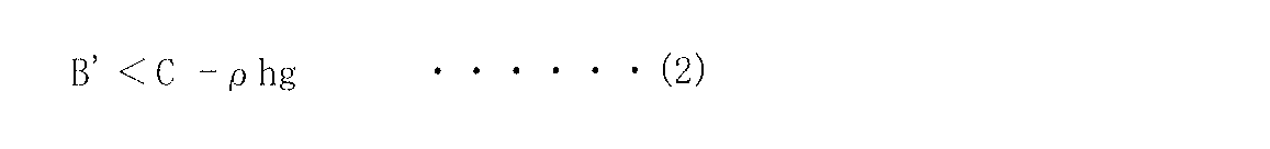

Fixing the second substrate on the first adhesive layer;
Forming a first functional layer on the second substrate;
Peeling the first substrate from the second substrate.
- 前記第1粘着層は、前記式(1)および式(2),(3)の両方を満たす、請求項1に記載の積層体の剥離方法。 The method according to claim 1, wherein the first adhesive layer satisfies both the formula (1) and the formulas (2) and (3).
- 前記第2基板の前記第1粘着層に固着する面に離型層を形成したのち、前記第1粘着層上に前記第2基板を固着する、請求項1に記載の積層体の剥離方法。 The method for peeling a laminate according to claim 1, wherein a release layer is formed on a surface of the second substrate that is fixed to the first adhesive layer, and then the second substrate is fixed on the first adhesive layer.
- 前記第1基板上に離型層を形成したのち、前記第1粘着層を形成する、請求項1に記載の積層体の剥離方法。 The method for peeling a laminate according to claim 1, wherein the first adhesive layer is formed after the release layer is formed on the first substrate.
- 前記離型層は無機材料により形成されている、請求項3に記載の積層体の剥離方法。 The laminate release method according to claim 3, wherein the release layer is formed of an inorganic material.
- 前記粘着層を介して前記第1基板に固着された前記第2基板上に、前記第1機能層を形成すると共に、前記第1機能層の周縁部に切り込みを入れたのち、前記第1機能層上に保護膜を形成する、請求項1に記載の積層体の剥離方法。 The first function layer is formed on the second substrate fixed to the first substrate via the adhesive layer, and the first function layer is cut after being cut into a peripheral portion of the first function layer. The peeling method of the laminated body of Claim 1 which forms a protective film on a layer.
- 第3基板上に第2粘着層を介して第4基板を固着することと、
前記第2基板と前記第4基板とを対向配置して貼り合わせることとを含み、
前記第2基板と前記第4基板とを貼り合わせたのち、前記第1基板および前記第3基板をこの順に剥離する、請求項1に記載の積層体の剥離方法。 Fixing the fourth substrate on the third substrate via the second adhesive layer;
Including arranging and bonding the second substrate and the fourth substrate opposite to each other,
The method for peeling a laminate according to claim 1, wherein the first substrate and the third substrate are peeled in this order after the second substrate and the fourth substrate are bonded together. - 前記第3基板上に前記第4基板を固着させたのち、前記第4基板上に第2機能層を形成する、請求項7に記載の積層体の剥離方法。 The method for peeling a laminate according to claim 7, wherein the second functional layer is formed on the fourth substrate after the fourth substrate is fixed on the third substrate.
- 前記第1機能層および前記第2機能層は半導体層、表示層およびカラーフィルタのうちのいずれかである、請求項8に記載の積層体の剥離方法。 The method for peeling a laminate according to claim 8, wherein the first functional layer and the second functional layer are any one of a semiconductor layer, a display layer, and a color filter.
- 前記第1基板および前記第3基板は剛性を有する、請求項7に記載の積層体の剥離方法。 The method for peeling a laminate according to claim 7, wherein the first substrate and the third substrate have rigidity.
- 前記第2基板および前記第4基板は可撓性を有する、請求項7に記載の積層体の剥離方法。 The method for peeling a laminate according to claim 7, wherein the second substrate and the fourth substrate have flexibility.
- 前記第2粘着層は前記式(1)および式(2),(3)の少なくとも一方を満たす粘着力を有する、請求項7に記載の積層体の剥離方法。 The method for peeling a laminate according to claim 7, wherein the second adhesive layer has an adhesive force satisfying at least one of the formulas (1), (2), and (3).
- 第1基板上に、粘着力が下記式(1)および式(2),(3)の少なくとも一方を満たす粘着層を形成することと、
前記粘着層上に可撓性を有する第2基板を固定することと、
前記第2基板上に機能層を形成することと、
前記第1基板を前記第2基板から剥離することと
を含む可撓性デバイスの製造方法。


Fixing a flexible second substrate on the adhesive layer;
Forming a functional layer on the second substrate;
Peeling the first substrate from the second substrate. A method for manufacturing a flexible device.
- 剛性を有する第1基板と、
可撓性を有する第2基板と、
粘着力が下記式(1)を満たす、前記第1基板と前記第2基板との間に設けられた粘着層と
を備えた積層体。
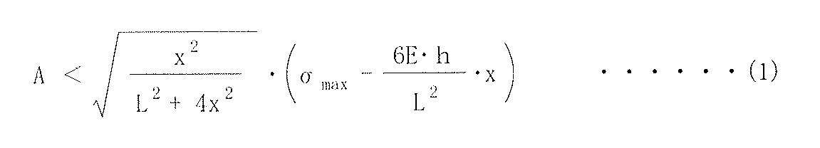
A second substrate having flexibility;
The laminated body provided with the adhesion layer provided between the said 1st board | substrate and the said 2nd board | substrate with which adhesive force satisfy | fills following formula (1).
Priority Applications (2)
| Application Number | Priority Date | Filing Date | Title |
|---|---|---|---|
| JP2016511884A JPWO2015152158A1 (en) | 2014-03-31 | 2015-03-30 | Laminated body, peeling method of laminated body, and manufacturing method of flexible device |
| US15/272,741 US10008670B2 (en) | 2014-03-31 | 2016-09-22 | Laminate, method of peeling laminate, and method of manufacturing flexible device |
Applications Claiming Priority (4)
| Application Number | Priority Date | Filing Date | Title |
|---|---|---|---|
| JP2014073330 | 2014-03-31 | ||
| JP2014-073330 | 2014-03-31 | ||
| JP2014212572 | 2014-10-17 | ||
| JP2014-212572 | 2014-10-17 |
Related Child Applications (1)
| Application Number | Title | Priority Date | Filing Date |
|---|---|---|---|
| US15/272,741 Continuation US10008670B2 (en) | 2014-03-31 | 2016-09-22 | Laminate, method of peeling laminate, and method of manufacturing flexible device |
Publications (1)
| Publication Number | Publication Date |
|---|---|
| WO2015152158A1 true WO2015152158A1 (en) | 2015-10-08 |
Family
ID=54240481
Family Applications (1)
| Application Number | Title | Priority Date | Filing Date |
|---|---|---|---|
| PCT/JP2015/059941 WO2015152158A1 (en) | 2014-03-31 | 2015-03-30 | Laminate, method for separating laminate and method for manufacturing flexible device |
Country Status (3)
| Country | Link |
|---|---|
| US (1) | US10008670B2 (en) |
| JP (1) | JPWO2015152158A1 (en) |
| WO (1) | WO2015152158A1 (en) |
Cited By (4)
| Publication number | Priority date | Publication date | Assignee | Title |
|---|---|---|---|---|
| CN107482133A (en) * | 2016-06-07 | 2017-12-15 | 株式会社迪恩士先端贴合科技 | The separation method and separator for the workpiece being made up of carrier substrate and resin bed |
| CN107591090A (en) * | 2016-07-06 | 2018-01-16 | 三星显示有限公司 | Rollable display device and rollable device |
| CN109949702A (en) * | 2019-03-25 | 2019-06-28 | 京东方科技集团股份有限公司 | A kind of flexible display apparatus and preparation method thereof |
| JP2019522809A (en) * | 2016-05-16 | 2019-08-15 | ダウ シリコーンズ コーポレーション | Adhesive release layer comprising at least one of silsesquioxane polymer and silane for display device substrate processing |
Families Citing this family (3)
| Publication number | Priority date | Publication date | Assignee | Title |
|---|---|---|---|---|
| JP6331969B2 (en) * | 2014-10-29 | 2018-05-30 | ソニー株式会社 | Method for manufacturing electronic device assembly |
| KR102362080B1 (en) * | 2017-05-31 | 2022-02-10 | 엘지디스플레이 주식회사 | Foldable display device |
| US11935977B2 (en) * | 2021-10-06 | 2024-03-19 | Massachusetts Institute Of Technology | Transferable ultra-thin substrates and related techniques |
Citations (5)
| Publication number | Priority date | Publication date | Assignee | Title |
|---|---|---|---|---|
| JP2012131664A (en) * | 2010-12-22 | 2012-07-12 | Nippon Electric Glass Co Ltd | Glass film laminate |
| JP2013035159A (en) * | 2011-08-04 | 2013-02-21 | Dainippon Printing Co Ltd | Glass film laminate, glass film laminate roll, glass film laminate with pixel for color filter, and method for producing glass film laminate |
| JP2013237159A (en) * | 2012-05-11 | 2013-11-28 | Nippon Electric Glass Co Ltd | Glass film laminate and method of manufacturing the same |
| JP2014008697A (en) * | 2012-06-29 | 2014-01-20 | Dainippon Printing Co Ltd | Glass film laminate |
| JP2014019597A (en) * | 2012-07-17 | 2014-02-03 | Nippon Electric Glass Co Ltd | Method for producing glass film, and glass film laminate |
Family Cites Families (32)
| Publication number | Priority date | Publication date | Assignee | Title |
|---|---|---|---|---|
| KR100278137B1 (en) * | 1997-09-04 | 2001-01-15 | 가나이 쓰도무 | Method of mounting semiconductor device and system thereof, method of manufacturing semiconductor device isolator and IC card |
| US6028772A (en) * | 1998-08-13 | 2000-02-22 | Lucent Technologies Inc. | Electronic assembly having improved resistance to delamination |
| US6460753B1 (en) * | 2000-11-01 | 2002-10-08 | Lucent Technologies Inc. | Bi-material assembly adhesively bonded at the ends and fabrication method |
| US20030116273A1 (en) * | 2001-10-01 | 2003-06-26 | Koichiro Nakamura | Method of bonding an optical part |
| CN100391004C (en) | 2002-10-30 | 2008-05-28 | 株式会社半导体能源研究所 | Semiconductor device and manufacturing method thereof |
| US20040191564A1 (en) * | 2002-12-17 | 2004-09-30 | Samsung Sdi Co., Ltd. | Donor film for low molecular weight full color organic electroluminescent device using laser induced thermal imaging method and method for fabricating low molecular weight full color organic electroluminescent device using the film |
| KR100611156B1 (en) * | 2003-11-29 | 2006-08-09 | 삼성에스디아이 주식회사 | Donor film for laser induced thermal imaging method and electroluminescence display device manufactured using the same film |
| KR100579174B1 (en) * | 2003-12-22 | 2006-05-11 | 삼성에스디아이 주식회사 | Donor film for laser induced thermal imaging method and electroluminescence display device manufactured using the same film |
| US8545962B2 (en) * | 2006-08-07 | 2013-10-01 | Paradigm Energy Research Corporation | Nano-fiber arrayed surfaces |
| US20110210407A1 (en) * | 2008-08-27 | 2011-09-01 | Youji Katayama | Double-faced adhesive film and electronic component module using same |
| GB0904582D0 (en) * | 2008-09-24 | 2009-04-29 | Lumina Adhesives | Switchable adhesives |
| US8692394B2 (en) * | 2009-09-30 | 2014-04-08 | Sekisui Chemical Co., Ltd. | Adhesive for semiconductor bonding, adhesive film for semiconductor bonding, method for mounting semiconductor chip, and semiconductor device |
| JP5505421B2 (en) * | 2009-11-13 | 2014-05-28 | 日立化成株式会社 | Method for manufacturing film adhesive, adhesive sheet, semiconductor device, and method for manufacturing the same |
| KR101783879B1 (en) * | 2010-01-13 | 2017-10-10 | 다우 코닝 도레이 캄파니 리미티드 | Silicone-based releasable adhesive composition, sheet-form substrate having releasable adhesive layer formed by curing this composition, and use of such as a protective film or fixing sheet |
| JP5651344B2 (en) * | 2010-02-04 | 2015-01-14 | 日東電工株式会社 | Thermally conductive double-sided adhesive sheet |
| EP2551323A1 (en) * | 2010-03-24 | 2013-01-30 | Sekisui Chemical Co., Ltd. | Adhesive composition, adhesive tape, method for processing semiconductor wafer and method for producing tsv wafer |
| WO2011145523A1 (en) * | 2010-05-19 | 2011-11-24 | 日東電工株式会社 | Thermally conductive adhesive sheet |
| EP2511092B1 (en) | 2010-07-28 | 2015-01-28 | Nippon Electric Glass Co., Ltd. | Glass film laminate |
| KR20120104450A (en) * | 2011-03-08 | 2012-09-21 | (주)엘지하우시스 | Pressure-sensitive adhesive composition for a film used for processing wafer |
| JP2012215737A (en) | 2011-04-01 | 2012-11-08 | Sony Corp | Manufacturing method of electronic device and display device |
| WO2013001959A1 (en) * | 2011-06-27 | 2013-01-03 | 電気化学工業株式会社 | Adhesive sheet |
| WO2013047435A1 (en) * | 2011-09-29 | 2013-04-04 | 日産化学工業株式会社 | Light-curing resin composition |
| JP6023538B2 (en) * | 2011-10-19 | 2016-11-09 | 日東電工株式会社 | Water-dispersible acrylic pressure-sensitive adhesive composition for re-peeling and pressure-sensitive adhesive sheet |
| JP5917215B2 (en) * | 2012-03-16 | 2016-05-11 | リンテック株式会社 | Adhesive composition, adhesive sheet, and method for manufacturing semiconductor device |
| JP6250265B2 (en) * | 2012-03-16 | 2017-12-20 | リンテック株式会社 | Adhesive composition, adhesive sheet, and method for manufacturing semiconductor device |
| FR2995447B1 (en) * | 2012-09-07 | 2014-09-05 | Soitec Silicon On Insulator | METHOD FOR SEPARATING AT LEAST TWO SUBSTRATES ACCORDING TO A CHOSEN INTERFACE |
| FR2995445B1 (en) * | 2012-09-07 | 2016-01-08 | Soitec Silicon On Insulator | METHOD OF MANUFACTURING A STRUCTURE FOR SUBSEQUENT SEPARATION |
| FR2995441B1 (en) * | 2012-09-07 | 2015-11-06 | Soitec Silicon On Insulator | DEVICE FOR SEPARATING TWO SUBSTRATES |
| WO2015133630A1 (en) * | 2014-03-07 | 2015-09-11 | 旭硝子株式会社 | Mold release film, method for manufacturing same, and method for manufacturing semiconductor package |
| JP6613894B2 (en) * | 2014-08-08 | 2019-12-04 | 東レ株式会社 | Temporary sticking adhesive, adhesive layer, wafer processed body and semiconductor device manufacturing method using the same, rework solvent, polyimide copolymer, polyimide mixed resin, and resin composition |
| KR20170044101A (en) * | 2014-08-20 | 2017-04-24 | 주식회사 쿠라레 | Acrylic adhesive composition and adhesive product |
| US10370528B2 (en) * | 2015-01-27 | 2019-08-06 | Kuraray Co., Ltd. | Acrylic block copolymer and adhesive composition |
-
2015
- 2015-03-30 JP JP2016511884A patent/JPWO2015152158A1/en active Pending
- 2015-03-30 WO PCT/JP2015/059941 patent/WO2015152158A1/en active Application Filing
-
2016
- 2016-09-22 US US15/272,741 patent/US10008670B2/en active Active
Patent Citations (5)
| Publication number | Priority date | Publication date | Assignee | Title |
|---|---|---|---|---|
| JP2012131664A (en) * | 2010-12-22 | 2012-07-12 | Nippon Electric Glass Co Ltd | Glass film laminate |
| JP2013035159A (en) * | 2011-08-04 | 2013-02-21 | Dainippon Printing Co Ltd | Glass film laminate, glass film laminate roll, glass film laminate with pixel for color filter, and method for producing glass film laminate |
| JP2013237159A (en) * | 2012-05-11 | 2013-11-28 | Nippon Electric Glass Co Ltd | Glass film laminate and method of manufacturing the same |
| JP2014008697A (en) * | 2012-06-29 | 2014-01-20 | Dainippon Printing Co Ltd | Glass film laminate |
| JP2014019597A (en) * | 2012-07-17 | 2014-02-03 | Nippon Electric Glass Co Ltd | Method for producing glass film, and glass film laminate |
Cited By (5)
| Publication number | Priority date | Publication date | Assignee | Title |
|---|---|---|---|---|
| JP2019522809A (en) * | 2016-05-16 | 2019-08-15 | ダウ シリコーンズ コーポレーション | Adhesive release layer comprising at least one of silsesquioxane polymer and silane for display device substrate processing |
| CN107482133A (en) * | 2016-06-07 | 2017-12-15 | 株式会社迪恩士先端贴合科技 | The separation method and separator for the workpiece being made up of carrier substrate and resin bed |
| CN107591090A (en) * | 2016-07-06 | 2018-01-16 | 三星显示有限公司 | Rollable display device and rollable device |
| CN109949702A (en) * | 2019-03-25 | 2019-06-28 | 京东方科技集团股份有限公司 | A kind of flexible display apparatus and preparation method thereof |
| CN109949702B (en) * | 2019-03-25 | 2024-01-02 | 京东方科技集团股份有限公司 | Flexible display device and manufacturing method thereof |
Also Published As
| Publication number | Publication date |
|---|---|
| US20170012202A1 (en) | 2017-01-12 |
| US10008670B2 (en) | 2018-06-26 |
| JPWO2015152158A1 (en) | 2017-04-13 |
Similar Documents
| Publication | Publication Date | Title |
|---|---|---|
| WO2015152158A1 (en) | Laminate, method for separating laminate and method for manufacturing flexible device | |
| US11360517B2 (en) | Flexible display apparatus | |
| KR102400871B1 (en) | Flexible display device and method for fabricating the same | |
| US11411189B2 (en) | Flexible OLED module stacked structure and manufacturing method thereof | |
| US11302766B2 (en) | Semiconductor unit, method of manufacturing the same, and electronic apparatus | |
| KR102348956B1 (en) | Multi vision display apparatus using a flexible display device | |
| KR102076519B1 (en) | Flexible display device and manufacturing method thereof | |
| US20170170425A1 (en) | Organic light emitting display device | |
| JP6826881B2 (en) | Protective member, display device and manufacturing method of display device | |
| KR20140122960A (en) | Flexible display panel | |
| KR20160016267A (en) | Flexible display device and method of fabricating thereof | |
| US20130308076A1 (en) | Flexible display and method for manufacturing the same | |
| TW201801308A (en) | Flexible display device | |
| JP2009199006A (en) | Liquid crystal display device and method for manufacturing the same | |
| US11462713B2 (en) | Display device and manufacturing method thereof | |
| US20210202868A1 (en) | Display apparatus | |
| WO2019092818A1 (en) | Method for attaching display panel and method for manufacturing display device | |
| WO2019049275A1 (en) | Production method for display device | |
| KR101951366B1 (en) | Flexible organic light emitting diode display device and bonding method of flexible printed circuit board | |
| KR102213438B1 (en) | Method of fabricating the flexible display device | |
| WO2021022405A1 (en) | Display device and manufacturing method for display device | |
| KR20200115757A (en) | Circuit board and method for manufacturing the circuit board | |
| JP2010107935A (en) | Flat panel display device and method of fabricating the same | |
| JP2012226013A (en) | Methods of manufacturing electronic device and display apparatus | |
| US20210063802A1 (en) | Electronic device and method for manufacturing the same |
Legal Events
| Date | Code | Title | Description |
|---|---|---|---|
| 121 | Ep: the epo has been informed by wipo that ep was designated in this application |
Ref document number: 15774257 Country of ref document: EP Kind code of ref document: A1 |
|
| ENP | Entry into the national phase |
Ref document number: 2016511884 Country of ref document: JP Kind code of ref document: A |
|
| NENP | Non-entry into the national phase | ||
| 122 | Ep: pct application non-entry in european phase |
Ref document number: 15774257 Country of ref document: EP Kind code of ref document: A1 |