WO2014050538A1 - Temporary adhesive for semiconductor device production, adhesive substrate using same, and semiconductor device production method - Google Patents
Temporary adhesive for semiconductor device production, adhesive substrate using same, and semiconductor device production method Download PDFInfo
- Publication number
- WO2014050538A1 WO2014050538A1 PCT/JP2013/074346 JP2013074346W WO2014050538A1 WO 2014050538 A1 WO2014050538 A1 WO 2014050538A1 JP 2013074346 W JP2013074346 W JP 2013074346W WO 2014050538 A1 WO2014050538 A1 WO 2014050538A1
- Authority
- WO
- WIPO (PCT)
- Prior art keywords
- group
- adhesive
- semiconductor device
- treated
- temporary
- Prior art date
Links
- 239000000853 adhesive Substances 0.000 title claims abstract description 237
- 230000001070 adhesive effect Effects 0.000 title claims abstract description 236
- 239000000758 substrate Substances 0.000 title claims abstract description 107
- 239000004065 semiconductor Substances 0.000 title claims abstract description 102
- 238000004519 manufacturing process Methods 0.000 title claims abstract description 56
- 150000001875 compounds Chemical class 0.000 claims abstract description 175
- 239000000178 monomer Substances 0.000 claims abstract description 86
- 229920000642 polymer Polymers 0.000 claims abstract description 83
- 239000007870 radical polymerization initiator Substances 0.000 claims abstract description 37
- 239000012790 adhesive layer Substances 0.000 claims description 108
- 125000001424 substituent group Chemical group 0.000 claims description 64
- 238000000034 method Methods 0.000 claims description 61
- 239000011241 protective layer Substances 0.000 claims description 56
- 230000005855 radiation Effects 0.000 claims description 36
- 125000004435 hydrogen atom Chemical group [H]* 0.000 claims description 29
- 239000002253 acid Substances 0.000 claims description 27
- 239000000126 substance Substances 0.000 claims description 19
- 238000010438 heat treatment Methods 0.000 claims description 18
- 239000003999 initiator Substances 0.000 claims description 17
- 238000011282 treatment Methods 0.000 claims description 16
- 229910052717 sulfur Inorganic materials 0.000 claims description 13
- 125000004430 oxygen atom Chemical group O* 0.000 claims description 12
- 125000004434 sulfur atom Chemical group 0.000 claims description 12
- 239000003505 polymerization initiator Substances 0.000 claims description 10
- 125000000843 phenylene group Chemical group C1(=C(C=CC=C1)*)* 0.000 claims description 5
- 238000005979 thermal decomposition reaction Methods 0.000 claims description 5
- 230000001678 irradiating effect Effects 0.000 claims description 4
- 239000012670 alkaline solution Substances 0.000 abstract 1
- 238000012993 chemical processing Methods 0.000 abstract 1
- 235000012431 wafers Nutrition 0.000 description 157
- -1 methacryloyl Chemical group 0.000 description 155
- XUIMIQQOPSSXEZ-UHFFFAOYSA-N Silicon Chemical compound [Si] XUIMIQQOPSSXEZ-UHFFFAOYSA-N 0.000 description 51
- 229910052710 silicon Inorganic materials 0.000 description 51
- 239000010703 silicon Substances 0.000 description 51
- 150000003254 radicals Chemical class 0.000 description 40
- 239000000975 dye Substances 0.000 description 37
- 125000003118 aryl group Chemical group 0.000 description 32
- 239000010410 layer Substances 0.000 description 30
- 125000001931 aliphatic group Chemical group 0.000 description 25
- 238000006116 polymerization reaction Methods 0.000 description 23
- NIXOWILDQLNWCW-UHFFFAOYSA-M Acrylate Chemical compound [O-]C(=O)C=C NIXOWILDQLNWCW-UHFFFAOYSA-M 0.000 description 22
- 125000000217 alkyl group Chemical group 0.000 description 21
- 239000004094 surface-active agent Substances 0.000 description 20
- 229920005989 resin Polymers 0.000 description 19
- 239000011347 resin Substances 0.000 description 19
- 230000008569 process Effects 0.000 description 18
- 125000003178 carboxy group Chemical group [H]OC(*)=O 0.000 description 17
- 239000000203 mixture Substances 0.000 description 16
- IAYPIBMASNFSPL-UHFFFAOYSA-N Ethylene oxide Chemical compound C1CO1 IAYPIBMASNFSPL-UHFFFAOYSA-N 0.000 description 15
- PEDCQBHIVMGVHV-UHFFFAOYSA-N Glycerine Chemical compound OCC(O)CO PEDCQBHIVMGVHV-UHFFFAOYSA-N 0.000 description 15
- PPBRXRYQALVLMV-UHFFFAOYSA-N Styrene Chemical compound C=CC1=CC=CC=C1 PPBRXRYQALVLMV-UHFFFAOYSA-N 0.000 description 14
- 235000014113 dietary fatty acids Nutrition 0.000 description 14
- 239000000194 fatty acid Substances 0.000 description 14
- 229930195729 fatty acid Natural products 0.000 description 14
- 125000002887 hydroxy group Chemical group [H]O* 0.000 description 14
- 230000002829 reductive effect Effects 0.000 description 14
- 239000000243 solution Substances 0.000 description 14
- 239000007787 solid Substances 0.000 description 13
- TXBCBTDQIULDIA-UHFFFAOYSA-N 2-[[3-hydroxy-2,2-bis(hydroxymethyl)propoxy]methyl]-2-(hydroxymethyl)propane-1,3-diol Chemical compound OCC(CO)(CO)COCC(CO)(CO)CO TXBCBTDQIULDIA-UHFFFAOYSA-N 0.000 description 12
- 239000007788 liquid Substances 0.000 description 12
- 229920001296 polysiloxane Polymers 0.000 description 12
- 239000002904 solvent Substances 0.000 description 12
- FBPFZTCFMRRESA-FSIIMWSLSA-N D-Glucitol Natural products OC[C@H](O)[C@H](O)[C@@H](O)[C@H](O)CO FBPFZTCFMRRESA-FSIIMWSLSA-N 0.000 description 11
- FBPFZTCFMRRESA-JGWLITMVSA-N D-glucitol Chemical compound OC[C@H](O)[C@@H](O)[C@H](O)[C@H](O)CO FBPFZTCFMRRESA-JGWLITMVSA-N 0.000 description 11
- 125000003647 acryloyl group Chemical group O=C([*])C([H])=C([H])[H] 0.000 description 11
- 239000011248 coating agent Substances 0.000 description 11
- 238000000576 coating method Methods 0.000 description 11
- 125000005843 halogen group Chemical group 0.000 description 11
- 239000000600 sorbitol Substances 0.000 description 11
- 125000004432 carbon atom Chemical group C* 0.000 description 10
- 239000003795 chemical substances by application Substances 0.000 description 10
- 230000001235 sensitizing effect Effects 0.000 description 10
- 150000002148 esters Chemical class 0.000 description 9
- 239000010408 film Substances 0.000 description 9
- 229910052731 fluorine Inorganic materials 0.000 description 9
- 150000002430 hydrocarbons Chemical group 0.000 description 9
- 125000002496 methyl group Chemical group [H]C([H])([H])* 0.000 description 9
- 238000010526 radical polymerization reaction Methods 0.000 description 9
- 230000035945 sensitivity Effects 0.000 description 9
- 230000008093 supporting effect Effects 0.000 description 9
- YCKRFDGAMUMZLT-UHFFFAOYSA-N Fluorine atom Chemical compound [F] YCKRFDGAMUMZLT-UHFFFAOYSA-N 0.000 description 8
- WSFSSNUMVMOOMR-UHFFFAOYSA-N Formaldehyde Chemical compound O=C WSFSSNUMVMOOMR-UHFFFAOYSA-N 0.000 description 8
- WYURNTSHIVDZCO-UHFFFAOYSA-N Tetrahydrofuran Chemical compound C1CCOC1 WYURNTSHIVDZCO-UHFFFAOYSA-N 0.000 description 8
- 150000001252 acrylic acid derivatives Chemical class 0.000 description 8
- 239000003513 alkali Substances 0.000 description 8
- 125000003545 alkoxy group Chemical group 0.000 description 8
- 125000003277 amino group Chemical group 0.000 description 8
- 230000015572 biosynthetic process Effects 0.000 description 8
- 239000011737 fluorine Substances 0.000 description 8
- 229920000058 polyacrylate Polymers 0.000 description 8
- 239000000047 product Substances 0.000 description 8
- ANRHNWWPFJCPAZ-UHFFFAOYSA-M thionine Chemical compound [Cl-].C1=CC(N)=CC2=[S+]C3=CC(N)=CC=C3N=C21 ANRHNWWPFJCPAZ-UHFFFAOYSA-M 0.000 description 8
- PAPBSGBWRJIAAV-UHFFFAOYSA-N ε-Caprolactone Chemical group O=C1CCCCCO1 PAPBSGBWRJIAAV-UHFFFAOYSA-N 0.000 description 8
- CERQOIWHTDAKMF-UHFFFAOYSA-N Methacrylic acid Chemical compound CC(=C)C(O)=O CERQOIWHTDAKMF-UHFFFAOYSA-N 0.000 description 7
- 229920003171 Poly (ethylene oxide) Polymers 0.000 description 7
- 238000010521 absorption reaction Methods 0.000 description 7
- NIXOWILDQLNWCW-UHFFFAOYSA-N acrylic acid group Chemical group C(C=C)(=O)O NIXOWILDQLNWCW-UHFFFAOYSA-N 0.000 description 7
- 125000004453 alkoxycarbonyl group Chemical group 0.000 description 7
- 150000001408 amides Chemical class 0.000 description 7
- 125000001495 ethyl group Chemical group [H]C([H])([H])C([H])([H])* 0.000 description 7
- 229920003986 novolac Polymers 0.000 description 7
- 150000002923 oximes Chemical class 0.000 description 7
- 229920000647 polyepoxide Polymers 0.000 description 7
- KWYUFKZDYYNOTN-UHFFFAOYSA-M potassium hydroxide Inorganic materials [OH-].[K+] KWYUFKZDYYNOTN-UHFFFAOYSA-M 0.000 description 7
- 238000012545 processing Methods 0.000 description 7
- 238000012360 testing method Methods 0.000 description 7
- RTZKZFJDLAIYFH-UHFFFAOYSA-N Diethyl ether Chemical compound CCOCC RTZKZFJDLAIYFH-UHFFFAOYSA-N 0.000 description 6
- 239000012965 benzophenone Substances 0.000 description 6
- 229910052799 carbon Inorganic materials 0.000 description 6
- 150000001732 carboxylic acid derivatives Chemical class 0.000 description 6
- 150000001735 carboxylic acids Chemical class 0.000 description 6
- 230000000052 comparative effect Effects 0.000 description 6
- 230000000694 effects Effects 0.000 description 6
- 239000003822 epoxy resin Substances 0.000 description 6
- 235000011187 glycerol Nutrition 0.000 description 6
- 229910052757 nitrogen Inorganic materials 0.000 description 6
- 230000036961 partial effect Effects 0.000 description 6
- WXZMFSXDPGVJKK-UHFFFAOYSA-N pentaerythritol Chemical compound OCC(CO)(CO)CO WXZMFSXDPGVJKK-UHFFFAOYSA-N 0.000 description 6
- 150000003839 salts Chemical class 0.000 description 6
- 238000000926 separation method Methods 0.000 description 6
- 150000005846 sugar alcohols Chemical class 0.000 description 6
- WGTYBPLFGIVFAS-UHFFFAOYSA-M tetramethylammonium hydroxide Chemical compound [OH-].C[N+](C)(C)C WGTYBPLFGIVFAS-UHFFFAOYSA-M 0.000 description 6
- HEQOJEGTZCTHCF-UHFFFAOYSA-N 2-amino-1-phenylethanone Chemical class NCC(=O)C1=CC=CC=C1 HEQOJEGTZCTHCF-UHFFFAOYSA-N 0.000 description 5
- LFQSCWFLJHTTHZ-UHFFFAOYSA-N Ethanol Chemical compound CCO LFQSCWFLJHTTHZ-UHFFFAOYSA-N 0.000 description 5
- QAOWNCQODCNURD-UHFFFAOYSA-N Sulfuric acid Chemical compound OS(O)(=O)=O QAOWNCQODCNURD-UHFFFAOYSA-N 0.000 description 5
- 150000001412 amines Chemical class 0.000 description 5
- 238000006243 chemical reaction Methods 0.000 description 5
- 238000000151 deposition Methods 0.000 description 5
- 125000004663 dialkyl amino group Chemical group 0.000 description 5
- 238000005516 engineering process Methods 0.000 description 5
- 230000001976 improved effect Effects 0.000 description 5
- 239000003112 inhibitor Substances 0.000 description 5
- 239000000463 material Substances 0.000 description 5
- 239000003960 organic solvent Substances 0.000 description 5
- 150000003573 thiols Chemical class 0.000 description 5
- 229920002554 vinyl polymer Polymers 0.000 description 5
- JYEUMXHLPRZUAT-UHFFFAOYSA-N 1,2,3-triazine Chemical group C1=CN=NN=C1 JYEUMXHLPRZUAT-UHFFFAOYSA-N 0.000 description 4
- KUDUQBURMYMBIJ-UHFFFAOYSA-N 2-prop-2-enoyloxyethyl prop-2-enoate Chemical compound C=CC(=O)OCCOC(=O)C=C KUDUQBURMYMBIJ-UHFFFAOYSA-N 0.000 description 4
- UJOBWOGCFQCDNV-UHFFFAOYSA-N 9H-carbazole Chemical compound C1=CC=C2C3=CC=CC=C3NC2=C1 UJOBWOGCFQCDNV-UHFFFAOYSA-N 0.000 description 4
- DKPFZGUDAPQIHT-UHFFFAOYSA-N Butyl acetate Natural products CCCCOC(C)=O DKPFZGUDAPQIHT-UHFFFAOYSA-N 0.000 description 4
- 239000004593 Epoxy Substances 0.000 description 4
- ISWSIDIOOBJBQZ-UHFFFAOYSA-N Phenol Chemical compound OC1=CC=CC=C1 ISWSIDIOOBJBQZ-UHFFFAOYSA-N 0.000 description 4
- 239000002202 Polyethylene glycol Substances 0.000 description 4
- 239000004820 Pressure-sensitive adhesive Substances 0.000 description 4
- ZJCCRDAZUWHFQH-UHFFFAOYSA-N Trimethylolpropane Chemical compound CCC(CO)(CO)CO ZJCCRDAZUWHFQH-UHFFFAOYSA-N 0.000 description 4
- 230000009471 action Effects 0.000 description 4
- 238000007259 addition reaction Methods 0.000 description 4
- 125000004450 alkenylene group Chemical group 0.000 description 4
- 239000003945 anionic surfactant Substances 0.000 description 4
- 150000008365 aromatic ketones Chemical class 0.000 description 4
- 125000001769 aryl amino group Chemical group 0.000 description 4
- 125000004104 aryloxy group Chemical group 0.000 description 4
- 150000001244 carboxylic acid anhydrides Chemical class 0.000 description 4
- 239000003093 cationic surfactant Substances 0.000 description 4
- 239000012986 chain transfer agent Substances 0.000 description 4
- 239000007795 chemical reaction product Substances 0.000 description 4
- 229920001577 copolymer Polymers 0.000 description 4
- 125000004093 cyano group Chemical group *C#N 0.000 description 4
- JHIVVAPYMSGYDF-UHFFFAOYSA-N cyclohexanone Chemical compound O=C1CCCCC1 JHIVVAPYMSGYDF-UHFFFAOYSA-N 0.000 description 4
- 230000008021 deposition Effects 0.000 description 4
- 238000000227 grinding Methods 0.000 description 4
- CATSNJVOTSVZJV-UHFFFAOYSA-N heptan-2-one Chemical compound CCCCCC(C)=O CATSNJVOTSVZJV-UHFFFAOYSA-N 0.000 description 4
- 125000001072 heteroaryl group Chemical group 0.000 description 4
- RKJUIXBNRJVNHR-UHFFFAOYSA-N indolenine group Chemical group N1=CCC2=CC=CC=C12 RKJUIXBNRJVNHR-UHFFFAOYSA-N 0.000 description 4
- 230000010354 integration Effects 0.000 description 4
- 239000012948 isocyanate Substances 0.000 description 4
- 150000002513 isocyanates Chemical class 0.000 description 4
- 125000005397 methacrylic acid ester group Chemical group 0.000 description 4
- 125000000449 nitro group Chemical group [O-][N+](*)=O 0.000 description 4
- 239000002736 nonionic surfactant Substances 0.000 description 4
- 150000001451 organic peroxides Chemical class 0.000 description 4
- CFJYNSNXFXLKNS-UHFFFAOYSA-N p-menthane Chemical compound CC(C)C1CCC(C)CC1 CFJYNSNXFXLKNS-UHFFFAOYSA-N 0.000 description 4
- 230000002093 peripheral effect Effects 0.000 description 4
- 125000001997 phenyl group Chemical group [H]C1=C([H])C([H])=C(*)C([H])=C1[H] 0.000 description 4
- 229920001223 polyethylene glycol Polymers 0.000 description 4
- 229920005749 polyurethane resin Polymers 0.000 description 4
- LLHKCFNBLRBOGN-UHFFFAOYSA-N propylene glycol methyl ether acetate Chemical compound COCC(C)OC(C)=O LLHKCFNBLRBOGN-UHFFFAOYSA-N 0.000 description 4
- 150000003384 small molecules Chemical class 0.000 description 4
- 238000003860 storage Methods 0.000 description 4
- 238000006467 substitution reaction Methods 0.000 description 4
- 125000000446 sulfanediyl group Chemical group *S* 0.000 description 4
- 125000000020 sulfo group Chemical group O=S(=O)([*])O[H] 0.000 description 4
- YXFVVABEGXRONW-UHFFFAOYSA-N toluene Substances CC1=CC=CC=C1 YXFVVABEGXRONW-UHFFFAOYSA-N 0.000 description 4
- XLYOFNOQVPJJNP-UHFFFAOYSA-N water Substances O XLYOFNOQVPJJNP-UHFFFAOYSA-N 0.000 description 4
- ARXJGSRGQADJSQ-UHFFFAOYSA-N 1-methoxypropan-2-ol Chemical compound COCC(C)O ARXJGSRGQADJSQ-UHFFFAOYSA-N 0.000 description 3
- ZWEHNKRNPOVVGH-UHFFFAOYSA-N 2-Butanone Chemical compound CCC(C)=O ZWEHNKRNPOVVGH-UHFFFAOYSA-N 0.000 description 3
- QTBSBXVTEAMEQO-UHFFFAOYSA-N Acetic acid Chemical compound CC(O)=O QTBSBXVTEAMEQO-UHFFFAOYSA-N 0.000 description 3
- CSCPPACGZOOCGX-UHFFFAOYSA-N Acetone Chemical compound CC(C)=O CSCPPACGZOOCGX-UHFFFAOYSA-N 0.000 description 3
- UHOVQNZJYSORNB-UHFFFAOYSA-N Benzene Chemical compound C1=CC=CC=C1 UHOVQNZJYSORNB-UHFFFAOYSA-N 0.000 description 3
- XEKOWRVHYACXOJ-UHFFFAOYSA-N Ethyl acetate Chemical compound CCOC(C)=O XEKOWRVHYACXOJ-UHFFFAOYSA-N 0.000 description 3
- LYCAIKOWRPUZTN-UHFFFAOYSA-N Ethylene glycol Chemical compound OCCO LYCAIKOWRPUZTN-UHFFFAOYSA-N 0.000 description 3
- WMFOQBRAJBCJND-UHFFFAOYSA-M Lithium hydroxide Chemical compound [Li+].[OH-] WMFOQBRAJBCJND-UHFFFAOYSA-M 0.000 description 3
- MUBZPKHOEPUJKR-UHFFFAOYSA-N Oxalic acid Chemical compound OC(=O)C(O)=O MUBZPKHOEPUJKR-UHFFFAOYSA-N 0.000 description 3
- XYFCBTPGUUZFHI-UHFFFAOYSA-N Phosphine Natural products P XYFCBTPGUUZFHI-UHFFFAOYSA-N 0.000 description 3
- NBIIXXVUZAFLBC-UHFFFAOYSA-N Phosphoric acid Chemical group OP(O)(O)=O NBIIXXVUZAFLBC-UHFFFAOYSA-N 0.000 description 3
- 239000004372 Polyvinyl alcohol Substances 0.000 description 3
- GOOHAUXETOMSMM-UHFFFAOYSA-N Propylene oxide Chemical compound CC1CO1 GOOHAUXETOMSMM-UHFFFAOYSA-N 0.000 description 3
- HEMHJVSKTPXQMS-UHFFFAOYSA-M Sodium hydroxide Chemical compound [OH-].[Na+] HEMHJVSKTPXQMS-UHFFFAOYSA-M 0.000 description 3
- ZMANZCXQSJIPKH-UHFFFAOYSA-N Triethylamine Chemical compound CCN(CC)CC ZMANZCXQSJIPKH-UHFFFAOYSA-N 0.000 description 3
- 239000006096 absorbing agent Substances 0.000 description 3
- 230000002378 acidificating effect Effects 0.000 description 3
- 125000005396 acrylic acid ester group Chemical group 0.000 description 3
- 238000012644 addition polymerization Methods 0.000 description 3
- 239000000654 additive Substances 0.000 description 3
- 125000003282 alkyl amino group Chemical group 0.000 description 3
- 150000004996 alkyl benzenes Chemical class 0.000 description 3
- 125000004390 alkyl sulfonyl group Chemical group 0.000 description 3
- 125000002947 alkylene group Chemical group 0.000 description 3
- 125000004429 atom Chemical group 0.000 description 3
- 239000000987 azo dye Substances 0.000 description 3
- 125000000751 azo group Chemical group [*]N=N[*] 0.000 description 3
- ZYGHJZDHTFUPRJ-UHFFFAOYSA-N benzo-alpha-pyrone Natural products C1=CC=C2OC(=O)C=CC2=C1 ZYGHJZDHTFUPRJ-UHFFFAOYSA-N 0.000 description 3
- ISAOCJYIOMOJEB-UHFFFAOYSA-N benzoin Chemical compound C=1C=CC=CC=1C(O)C(=O)C1=CC=CC=C1 ISAOCJYIOMOJEB-UHFFFAOYSA-N 0.000 description 3
- RWCCWEUUXYIKHB-UHFFFAOYSA-N benzophenone Chemical compound C=1C=CC=CC=1C(=O)C1=CC=CC=C1 RWCCWEUUXYIKHB-UHFFFAOYSA-N 0.000 description 3
- 150000001721 carbon Chemical group 0.000 description 3
- 150000001733 carboxylic acid esters Chemical class 0.000 description 3
- 235000001671 coumarin Nutrition 0.000 description 3
- 150000004775 coumarins Chemical class 0.000 description 3
- 125000004122 cyclic group Chemical group 0.000 description 3
- UAOMVDZJSHZZME-UHFFFAOYSA-N diisopropylamine Chemical compound CC(C)NC(C)C UAOMVDZJSHZZME-UHFFFAOYSA-N 0.000 description 3
- 239000000539 dimer Substances 0.000 description 3
- 238000010894 electron beam technology Methods 0.000 description 3
- 125000003700 epoxy group Chemical group 0.000 description 3
- UHESRSKEBRADOO-UHFFFAOYSA-N ethyl carbamate;prop-2-enoic acid Chemical class OC(=O)C=C.CCOC(N)=O UHESRSKEBRADOO-UHFFFAOYSA-N 0.000 description 3
- 150000004665 fatty acids Chemical class 0.000 description 3
- 125000000524 functional group Chemical group 0.000 description 3
- 150000008282 halocarbons Chemical class 0.000 description 3
- 229910052736 halogen Inorganic materials 0.000 description 3
- 230000001771 impaired effect Effects 0.000 description 3
- IQPQWNKOIGAROB-UHFFFAOYSA-N isocyanate group Chemical group [N-]=C=O IQPQWNKOIGAROB-UHFFFAOYSA-N 0.000 description 3
- LZCLXQDLBQLTDK-UHFFFAOYSA-N lactic acid ethyl ester Natural products CCOC(=O)C(C)O LZCLXQDLBQLTDK-UHFFFAOYSA-N 0.000 description 3
- 238000005259 measurement Methods 0.000 description 3
- 229910052751 metal Inorganic materials 0.000 description 3
- 239000002184 metal Substances 0.000 description 3
- WCPAKWJPBJAGKN-UHFFFAOYSA-N oxadiazole Chemical group C1=CON=N1 WCPAKWJPBJAGKN-UHFFFAOYSA-N 0.000 description 3
- 229910000073 phosphorus hydride Inorganic materials 0.000 description 3
- 239000000049 pigment Substances 0.000 description 3
- 229920002037 poly(vinyl butyral) polymer Polymers 0.000 description 3
- 229920006324 polyoxymethylene Polymers 0.000 description 3
- 229920002451 polyvinyl alcohol Polymers 0.000 description 3
- 238000007142 ring opening reaction Methods 0.000 description 3
- 125000005504 styryl group Chemical group 0.000 description 3
- 125000005156 substituted alkylene group Chemical group 0.000 description 3
- 150000003871 sulfonates Chemical class 0.000 description 3
- YLQBMQCUIZJEEH-UHFFFAOYSA-N tetrahydrofuran Natural products C=1C=COC=1 YLQBMQCUIZJEEH-UHFFFAOYSA-N 0.000 description 3
- QXJQHYBHAIHNGG-UHFFFAOYSA-N trimethylolethane Chemical compound OCC(C)(CO)CO QXJQHYBHAIHNGG-UHFFFAOYSA-N 0.000 description 3
- 125000000391 vinyl group Chemical group [H]C([*])=C([H])[H] 0.000 description 3
- MUTGBJKUEZFXGO-OLQVQODUSA-N (3as,7ar)-3a,4,5,6,7,7a-hexahydro-2-benzofuran-1,3-dione Chemical compound C1CCC[C@@H]2C(=O)OC(=O)[C@@H]21 MUTGBJKUEZFXGO-OLQVQODUSA-N 0.000 description 2
- KMOUUZVZFBCRAM-OLQVQODUSA-N (3as,7ar)-3a,4,7,7a-tetrahydro-2-benzofuran-1,3-dione Chemical compound C1C=CC[C@@H]2C(=O)OC(=O)[C@@H]21 KMOUUZVZFBCRAM-OLQVQODUSA-N 0.000 description 2
- DNIAPMSPPWPWGF-GSVOUGTGSA-N (R)-(-)-Propylene glycol Chemical compound C[C@@H](O)CO DNIAPMSPPWPWGF-GSVOUGTGSA-N 0.000 description 2
- WKBPZYKAUNRMKP-UHFFFAOYSA-N 1-[2-(2,4-dichlorophenyl)pentyl]1,2,4-triazole Chemical compound C=1C=C(Cl)C=C(Cl)C=1C(CCC)CN1C=NC=N1 WKBPZYKAUNRMKP-UHFFFAOYSA-N 0.000 description 2
- XUVKSPPGPPFPQN-UHFFFAOYSA-N 10-Methyl-9(10H)-acridone Chemical compound C1=CC=C2N(C)C3=CC=CC=C3C(=O)C2=C1 XUVKSPPGPPFPQN-UHFFFAOYSA-N 0.000 description 2
- INQDDHNZXOAFFD-UHFFFAOYSA-N 2-[2-(2-prop-2-enoyloxyethoxy)ethoxy]ethyl prop-2-enoate Chemical compound C=CC(=O)OCCOCCOCCOC(=O)C=C INQDDHNZXOAFFD-UHFFFAOYSA-N 0.000 description 2
- UHFFVFAKEGKNAQ-UHFFFAOYSA-N 2-benzyl-2-(dimethylamino)-1-(4-morpholin-4-ylphenyl)butan-1-one Chemical compound C=1C=C(N2CCOCC2)C=CC=1C(=O)C(CC)(N(C)C)CC1=CC=CC=C1 UHFFVFAKEGKNAQ-UHFFFAOYSA-N 0.000 description 2
- SVONRAPFKPVNKG-UHFFFAOYSA-N 2-ethoxyethyl acetate Chemical compound CCOCCOC(C)=O SVONRAPFKPVNKG-UHFFFAOYSA-N 0.000 description 2
- KBKNKFIRGXQLDB-UHFFFAOYSA-N 2-fluoroethenylbenzene Chemical compound FC=CC1=CC=CC=C1 KBKNKFIRGXQLDB-UHFFFAOYSA-N 0.000 description 2
- PCKZAVNWRLEHIP-UHFFFAOYSA-N 2-hydroxy-1-[4-[[4-(2-hydroxy-2-methylpropanoyl)phenyl]methyl]phenyl]-2-methylpropan-1-one Chemical compound C1=CC(C(=O)C(C)(O)C)=CC=C1CC1=CC=C(C(=O)C(C)(C)O)C=C1 PCKZAVNWRLEHIP-UHFFFAOYSA-N 0.000 description 2
- XLLIQLLCWZCATF-UHFFFAOYSA-N 2-methoxyethyl acetate Chemical compound COCCOC(C)=O XLLIQLLCWZCATF-UHFFFAOYSA-N 0.000 description 2
- LWRBVKNFOYUCNP-UHFFFAOYSA-N 2-methyl-1-(4-methylsulfanylphenyl)-2-morpholin-4-ylpropan-1-one Chemical compound C1=CC(SC)=CC=C1C(=O)C(C)(C)N1CCOCC1 LWRBVKNFOYUCNP-UHFFFAOYSA-N 0.000 description 2
- NJWGQARXZDRHCD-UHFFFAOYSA-N 2-methylanthraquinone Chemical compound C1=CC=C2C(=O)C3=CC(C)=CC=C3C(=O)C2=C1 NJWGQARXZDRHCD-UHFFFAOYSA-N 0.000 description 2
- QTWJRLJHJPIABL-UHFFFAOYSA-N 2-methylphenol;3-methylphenol;4-methylphenol Chemical compound CC1=CC=C(O)C=C1.CC1=CC=CC(O)=C1.CC1=CC=CC=C1O QTWJRLJHJPIABL-UHFFFAOYSA-N 0.000 description 2
- MIUYEAQDHPVUNY-UHFFFAOYSA-N 2-naphthalen-1-yl-5-(trichloromethyl)-1,3,4-oxadiazole Chemical compound O1C(C(Cl)(Cl)Cl)=NN=C1C1=CC=CC2=CC=CC=C12 MIUYEAQDHPVUNY-UHFFFAOYSA-N 0.000 description 2
- 125000003903 2-propenyl group Chemical group [H]C([*])([H])C([H])=C([H])[H] 0.000 description 2
- GOLORTLGFDVFDW-UHFFFAOYSA-N 3-(1h-benzimidazol-2-yl)-7-(diethylamino)chromen-2-one Chemical compound C1=CC=C2NC(C3=CC4=CC=C(C=C4OC3=O)N(CC)CC)=NC2=C1 GOLORTLGFDVFDW-UHFFFAOYSA-N 0.000 description 2
- KEPGNQLKWDULGD-UHFFFAOYSA-N 3-(3-prop-2-enoyloxypropoxy)propyl prop-2-enoate Chemical compound C=CC(=O)OCCCOCCCOC(=O)C=C KEPGNQLKWDULGD-UHFFFAOYSA-N 0.000 description 2
- TXFPEBPIARQUIG-UHFFFAOYSA-N 4'-hydroxyacetophenone Chemical compound CC(=O)C1=CC=C(O)C=C1 TXFPEBPIARQUIG-UHFFFAOYSA-N 0.000 description 2
- VVBLNCFGVYUYGU-UHFFFAOYSA-N 4,4'-Bis(dimethylamino)benzophenone Chemical compound C1=CC(N(C)C)=CC=C1C(=O)C1=CC=C(N(C)C)C=C1 VVBLNCFGVYUYGU-UHFFFAOYSA-N 0.000 description 2
- KWOLFJPFCHCOCG-UHFFFAOYSA-N Acetophenone Natural products CC(=O)C1=CC=CC=C1 KWOLFJPFCHCOCG-UHFFFAOYSA-N 0.000 description 2
- ATRRKUHOCOJYRX-UHFFFAOYSA-N Ammonium bicarbonate Chemical compound [NH4+].OC([O-])=O ATRRKUHOCOJYRX-UHFFFAOYSA-N 0.000 description 2
- KWIUHFFTVRNATP-UHFFFAOYSA-N Betaine Natural products C[N+](C)(C)CC([O-])=O KWIUHFFTVRNATP-UHFFFAOYSA-N 0.000 description 2
- ZTQSAGDEMFDKMZ-UHFFFAOYSA-N Butyraldehyde Chemical compound CCCC=O ZTQSAGDEMFDKMZ-UHFFFAOYSA-N 0.000 description 2
- OKTJSMMVPCPJKN-UHFFFAOYSA-N Carbon Chemical compound [C] OKTJSMMVPCPJKN-UHFFFAOYSA-N 0.000 description 2
- RGHNJXZEOKUKBD-SQOUGZDYSA-N D-gluconic acid Chemical compound OC[C@@H](O)[C@@H](O)[C@H](O)[C@@H](O)C(O)=O RGHNJXZEOKUKBD-SQOUGZDYSA-N 0.000 description 2
- JOYRKODLDBILNP-UHFFFAOYSA-N Ethyl urethane Chemical compound CCOC(N)=O JOYRKODLDBILNP-UHFFFAOYSA-N 0.000 description 2
- QUSNBJAOOMFDIB-UHFFFAOYSA-N Ethylamine Chemical compound CCN QUSNBJAOOMFDIB-UHFFFAOYSA-N 0.000 description 2
- 239000005977 Ethylene Substances 0.000 description 2
- QIGBRXMKCJKVMJ-UHFFFAOYSA-N Hydroquinone Chemical compound OC1=CC=C(O)C=C1 QIGBRXMKCJKVMJ-UHFFFAOYSA-N 0.000 description 2
- FFOPEPMHKILNIT-UHFFFAOYSA-N Isopropyl butyrate Chemical compound CCCC(=O)OC(C)C FFOPEPMHKILNIT-UHFFFAOYSA-N 0.000 description 2
- CERQOIWHTDAKMF-UHFFFAOYSA-M Methacrylate Chemical compound CC(=C)C([O-])=O CERQOIWHTDAKMF-UHFFFAOYSA-M 0.000 description 2
- AFVFQIVMOAPDHO-UHFFFAOYSA-N Methanesulfonic acid Chemical compound CS(O)(=O)=O AFVFQIVMOAPDHO-UHFFFAOYSA-N 0.000 description 2
- BAPJBEWLBFYGME-UHFFFAOYSA-N Methyl acrylate Chemical compound COC(=O)C=C BAPJBEWLBFYGME-UHFFFAOYSA-N 0.000 description 2
- GYCMBHHDWRMZGG-UHFFFAOYSA-N Methylacrylonitrile Chemical class CC(=C)C#N GYCMBHHDWRMZGG-UHFFFAOYSA-N 0.000 description 2
- IMNFDUFMRHMDMM-UHFFFAOYSA-N N-Heptane Chemical compound CCCCCCC IMNFDUFMRHMDMM-UHFFFAOYSA-N 0.000 description 2
- 239000004695 Polyether sulfone Substances 0.000 description 2
- 239000004698 Polyethylene Substances 0.000 description 2
- 239000004793 Polystyrene Substances 0.000 description 2
- ATUOYWHBWRKTHZ-UHFFFAOYSA-N Propane Chemical compound CCC ATUOYWHBWRKTHZ-UHFFFAOYSA-N 0.000 description 2
- OFOBLEOULBTSOW-UHFFFAOYSA-N Propanedioic acid Natural products OC(=O)CC(O)=O OFOBLEOULBTSOW-UHFFFAOYSA-N 0.000 description 2
- JUJWROOIHBZHMG-UHFFFAOYSA-N Pyridine Chemical compound C1=CC=NC=C1 JUJWROOIHBZHMG-UHFFFAOYSA-N 0.000 description 2
- CDBYLPFSWZWCQE-UHFFFAOYSA-L Sodium Carbonate Chemical compound [Na+].[Na+].[O-]C([O-])=O CDBYLPFSWZWCQE-UHFFFAOYSA-L 0.000 description 2
- UIIMBOGNXHQVGW-UHFFFAOYSA-M Sodium bicarbonate Chemical compound [Na+].OC([O-])=O UIIMBOGNXHQVGW-UHFFFAOYSA-M 0.000 description 2
- 244000028419 Styrax benzoin Species 0.000 description 2
- 235000000126 Styrax benzoin Nutrition 0.000 description 2
- 235000008411 Sumatra benzointree Nutrition 0.000 description 2
- DAKWPKUUDNSNPN-UHFFFAOYSA-N Trimethylolpropane triacrylate Chemical compound C=CC(=O)OCC(CC)(COC(=O)C=C)COC(=O)C=C DAKWPKUUDNSNPN-UHFFFAOYSA-N 0.000 description 2
- CQHKDHVZYZUZMJ-UHFFFAOYSA-N [2,2-bis(hydroxymethyl)-3-prop-2-enoyloxypropyl] prop-2-enoate Chemical compound C=CC(=O)OCC(CO)(CO)COC(=O)C=C CQHKDHVZYZUZMJ-UHFFFAOYSA-N 0.000 description 2
- MPIAGWXWVAHQBB-UHFFFAOYSA-N [3-prop-2-enoyloxy-2-[[3-prop-2-enoyloxy-2,2-bis(prop-2-enoyloxymethyl)propoxy]methyl]-2-(prop-2-enoyloxymethyl)propyl] prop-2-enoate Chemical compound C=CC(=O)OCC(COC(=O)C=C)(COC(=O)C=C)COCC(COC(=O)C=C)(COC(=O)C=C)COC(=O)C=C MPIAGWXWVAHQBB-UHFFFAOYSA-N 0.000 description 2
- 239000011354 acetal resin Substances 0.000 description 2
- 150000003926 acrylamides Chemical class 0.000 description 2
- 150000001298 alcohols Chemical class 0.000 description 2
- 125000004419 alkynylene group Chemical group 0.000 description 2
- 238000007112 amidation reaction Methods 0.000 description 2
- 239000001099 ammonium carbonate Substances 0.000 description 2
- 229940053200 antiepileptics fatty acid derivative Drugs 0.000 description 2
- 239000007864 aqueous solution Substances 0.000 description 2
- 125000004391 aryl sulfonyl group Chemical group 0.000 description 2
- 230000008901 benefit Effects 0.000 description 2
- 229960002130 benzoin Drugs 0.000 description 2
- 229960003237 betaine Drugs 0.000 description 2
- 229920001400 block copolymer Polymers 0.000 description 2
- 238000009835 boiling Methods 0.000 description 2
- GKRVGTLVYRYCFR-UHFFFAOYSA-N butane-1,4-diol;2-methylidenebutanedioic acid Chemical compound OCCCCO.OC(=O)CC(=C)C(O)=O.OC(=O)CC(=C)C(O)=O GKRVGTLVYRYCFR-UHFFFAOYSA-N 0.000 description 2
- CQEYYJKEWSMYFG-UHFFFAOYSA-N butyl acrylate Chemical compound CCCCOC(=O)C=C CQEYYJKEWSMYFG-UHFFFAOYSA-N 0.000 description 2
- XUPYJHCZDLZNFP-UHFFFAOYSA-N butyl butanoate Chemical compound CCCCOC(=O)CCC XUPYJHCZDLZNFP-UHFFFAOYSA-N 0.000 description 2
- 125000002915 carbonyl group Chemical group [*:2]C([*:1])=O 0.000 description 2
- KRKNYBCHXYNGOX-UHFFFAOYSA-N citric acid Natural products OC(=O)CC(O)(C(O)=O)CC(O)=O KRKNYBCHXYNGOX-UHFFFAOYSA-N 0.000 description 2
- 239000013065 commercial product Substances 0.000 description 2
- 238000006482 condensation reaction Methods 0.000 description 2
- 229930003836 cresol Natural products 0.000 description 2
- 238000004132 cross linking Methods 0.000 description 2
- LDHQCZJRKDOVOX-NSCUHMNNSA-N crotonic acid Chemical compound C\C=C\C(O)=O LDHQCZJRKDOVOX-NSCUHMNNSA-N 0.000 description 2
- SBZXBUIDTXKZTM-UHFFFAOYSA-N diglyme Chemical compound COCCOCCOC SBZXBUIDTXKZTM-UHFFFAOYSA-N 0.000 description 2
- USIUVYZYUHIAEV-UHFFFAOYSA-N diphenyl ether Natural products C=1C=CC=CC=1OC1=CC=CC=C1 USIUVYZYUHIAEV-UHFFFAOYSA-N 0.000 description 2
- 238000004090 dissolution Methods 0.000 description 2
- UKMSUNONTOPOIO-UHFFFAOYSA-N docosanoic acid Chemical compound CCCCCCCCCCCCCCCCCCCCCC(O)=O UKMSUNONTOPOIO-UHFFFAOYSA-N 0.000 description 2
- 238000001035 drying Methods 0.000 description 2
- 125000006575 electron-withdrawing group Chemical group 0.000 description 2
- 238000005886 esterification reaction Methods 0.000 description 2
- BHXIWUJLHYHGSJ-UHFFFAOYSA-N ethyl 3-ethoxypropanoate Chemical compound CCOCCC(=O)OCC BHXIWUJLHYHGSJ-UHFFFAOYSA-N 0.000 description 2
- 229940116333 ethyl lactate Drugs 0.000 description 2
- 235000019382 gum benzoic Nutrition 0.000 description 2
- NGAZZOYFWWSOGK-UHFFFAOYSA-N heptan-3-one Chemical compound CCCCC(=O)CC NGAZZOYFWWSOGK-UHFFFAOYSA-N 0.000 description 2
- 125000005842 heteroatom Chemical group 0.000 description 2
- FUZZWVXGSFPDMH-UHFFFAOYSA-M hexanoate Chemical compound CCCCCC([O-])=O FUZZWVXGSFPDMH-UHFFFAOYSA-M 0.000 description 2
- 229910052739 hydrogen Inorganic materials 0.000 description 2
- 230000000977 initiatory effect Effects 0.000 description 2
- 229910052740 iodine Inorganic materials 0.000 description 2
- XEEYBQQBJWHFJM-UHFFFAOYSA-N iron Substances [Fe] XEEYBQQBJWHFJM-UHFFFAOYSA-N 0.000 description 2
- 229910052742 iron Inorganic materials 0.000 description 2
- GJRQTCIYDGXPES-UHFFFAOYSA-N iso-butyl acetate Natural products CC(C)COC(C)=O GJRQTCIYDGXPES-UHFFFAOYSA-N 0.000 description 2
- MLFHJEHSLIIPHL-UHFFFAOYSA-N isoamyl acetate Chemical compound CC(C)CCOC(C)=O MLFHJEHSLIIPHL-UHFFFAOYSA-N 0.000 description 2
- FGKJLKRYENPLQH-UHFFFAOYSA-M isocaproate Chemical compound CC(C)CCC([O-])=O FGKJLKRYENPLQH-UHFFFAOYSA-M 0.000 description 2
- LDHQCZJRKDOVOX-IHWYPQMZSA-N isocrotonic acid Chemical compound C\C=C/C(O)=O LDHQCZJRKDOVOX-IHWYPQMZSA-N 0.000 description 2
- ZFSLODLOARCGLH-UHFFFAOYSA-N isocyanuric acid Chemical compound OC1=NC(O)=NC(O)=N1 ZFSLODLOARCGLH-UHFFFAOYSA-N 0.000 description 2
- OQAGVSWESNCJJT-UHFFFAOYSA-N isovaleric acid methyl ester Natural products COC(=O)CC(C)C OQAGVSWESNCJJT-UHFFFAOYSA-N 0.000 description 2
- JVTAAEKCZFNVCJ-UHFFFAOYSA-N lactic acid Chemical compound CC(O)C(O)=O JVTAAEKCZFNVCJ-UHFFFAOYSA-N 0.000 description 2
- VZCYOOQTPOCHFL-UPHRSURJSA-N maleic acid Chemical compound OC(=O)\C=C/C(O)=O VZCYOOQTPOCHFL-UPHRSURJSA-N 0.000 description 2
- 239000011976 maleic acid Substances 0.000 description 2
- 150000002734 metacrylic acid derivatives Chemical class 0.000 description 2
- FQPSGWSUVKBHSU-UHFFFAOYSA-N methacrylamide Chemical class CC(=C)C(N)=O FQPSGWSUVKBHSU-UHFFFAOYSA-N 0.000 description 2
- BDAGIHXWWSANSR-UHFFFAOYSA-N methanoic acid Natural products OC=O BDAGIHXWWSANSR-UHFFFAOYSA-N 0.000 description 2
- HSDFKDZBJMDHFF-UHFFFAOYSA-N methyl 3-ethoxypropanoate Chemical compound CCOCCC(=O)OC HSDFKDZBJMDHFF-UHFFFAOYSA-N 0.000 description 2
- BDJSOPWXYLFTNW-UHFFFAOYSA-N methyl 3-methoxypropanoate Chemical compound COCCC(=O)OC BDJSOPWXYLFTNW-UHFFFAOYSA-N 0.000 description 2
- LVHBHZANLOWSRM-UHFFFAOYSA-N methylenebutanedioic acid Natural products OC(=O)CC(=C)C(O)=O LVHBHZANLOWSRM-UHFFFAOYSA-N 0.000 description 2
- 230000004048 modification Effects 0.000 description 2
- 238000012986 modification Methods 0.000 description 2
- SGCOOLQXTVQUQF-UHFFFAOYSA-N naphthalen-1-ol;oxirane Chemical compound C1CO1.C1=CC=C2C(O)=CC=CC2=C1 SGCOOLQXTVQUQF-UHFFFAOYSA-N 0.000 description 2
- 230000000269 nucleophilic effect Effects 0.000 description 2
- 150000004010 onium ions Chemical class 0.000 description 2
- 230000003287 optical effect Effects 0.000 description 2
- VSXGXPNADZQTGQ-UHFFFAOYSA-N oxirane;phenol Chemical compound C1CO1.OC1=CC=CC=C1 VSXGXPNADZQTGQ-UHFFFAOYSA-N 0.000 description 2
- 229910052760 oxygen Inorganic materials 0.000 description 2
- 229930004008 p-menthane Natural products 0.000 description 2
- VLTRZXGMWDSKGL-UHFFFAOYSA-M perchlorate Chemical compound [O-]Cl(=O)(=O)=O VLTRZXGMWDSKGL-UHFFFAOYSA-M 0.000 description 2
- 230000000704 physical effect Effects 0.000 description 2
- 238000005498 polishing Methods 0.000 description 2
- 229920006122 polyamide resin Polymers 0.000 description 2
- 239000004417 polycarbonate Substances 0.000 description 2
- 229920000515 polycarbonate Polymers 0.000 description 2
- 229920000728 polyester Polymers 0.000 description 2
- 229920001225 polyester resin Polymers 0.000 description 2
- 239000004645 polyester resin Substances 0.000 description 2
- 229920006393 polyether sulfone Polymers 0.000 description 2
- 229920000573 polyethylene Polymers 0.000 description 2
- 229920000098 polyolefin Polymers 0.000 description 2
- 229920001451 polypropylene glycol Polymers 0.000 description 2
- 229920002223 polystyrene Polymers 0.000 description 2
- 229920002689 polyvinyl acetate Polymers 0.000 description 2
- 239000011118 polyvinyl acetate Substances 0.000 description 2
- BWHMMNNQKKPAPP-UHFFFAOYSA-L potassium carbonate Chemical compound [K+].[K+].[O-]C([O-])=O BWHMMNNQKKPAPP-UHFFFAOYSA-L 0.000 description 2
- 125000002924 primary amino group Chemical group [H]N([H])* 0.000 description 2
- 230000001681 protective effect Effects 0.000 description 2
- WQGWDDDVZFFDIG-UHFFFAOYSA-N pyrogallol Chemical compound OC1=CC=CC(O)=C1O WQGWDDDVZFFDIG-UHFFFAOYSA-N 0.000 description 2
- WVIICGIFSIBFOG-UHFFFAOYSA-N pyrylium Chemical class C1=CC=[O+]C=C1 WVIICGIFSIBFOG-UHFFFAOYSA-N 0.000 description 2
- 230000009467 reduction Effects 0.000 description 2
- 238000007127 saponification reaction Methods 0.000 description 2
- 235000015424 sodium Nutrition 0.000 description 2
- MSFGZHUJTJBYFA-UHFFFAOYSA-M sodium dichloroisocyanurate Chemical compound [Na+].ClN1C(=O)[N-]C(=O)N(Cl)C1=O MSFGZHUJTJBYFA-UHFFFAOYSA-M 0.000 description 2
- GJBRNHKUVLOCEB-UHFFFAOYSA-N tert-butyl benzenecarboperoxoate Chemical compound CC(C)(C)OOC(=O)C1=CC=CC=C1 GJBRNHKUVLOCEB-UHFFFAOYSA-N 0.000 description 2
- 229920001187 thermosetting polymer Polymers 0.000 description 2
- 125000003396 thiol group Chemical group [H]S* 0.000 description 2
- JOXIMZWYDAKGHI-UHFFFAOYSA-N toluene-4-sulfonic acid Chemical compound CC1=CC=C(S(O)(=O)=O)C=C1 JOXIMZWYDAKGHI-UHFFFAOYSA-N 0.000 description 2
- VZCYOOQTPOCHFL-UHFFFAOYSA-N trans-butenedioic acid Natural products OC(=O)C=CC(O)=O VZCYOOQTPOCHFL-UHFFFAOYSA-N 0.000 description 2
- LDHQCZJRKDOVOX-UHFFFAOYSA-N trans-crotonic acid Natural products CC=CC(O)=O LDHQCZJRKDOVOX-UHFFFAOYSA-N 0.000 description 2
- 238000012546 transfer Methods 0.000 description 2
- 125000004953 trihalomethyl group Chemical group 0.000 description 2
- GETQZCLCWQTVFV-UHFFFAOYSA-N trimethylamine Chemical compound CN(C)C GETQZCLCWQTVFV-UHFFFAOYSA-N 0.000 description 2
- LWIHDJKSTIGBAC-UHFFFAOYSA-K tripotassium phosphate Chemical compound [K+].[K+].[K+].[O-]P([O-])([O-])=O LWIHDJKSTIGBAC-UHFFFAOYSA-K 0.000 description 2
- 229930195735 unsaturated hydrocarbon Natural products 0.000 description 2
- 150000003673 urethanes Chemical class 0.000 description 2
- JNELGWHKGNBSMD-UHFFFAOYSA-N xanthone Chemical compound C1=CC=C2C(=O)C3=CC=CC=C3OC2=C1 JNELGWHKGNBSMD-UHFFFAOYSA-N 0.000 description 2
- QNODIIQQMGDSEF-UHFFFAOYSA-N (1-hydroxycyclohexyl)-phenylmethanone Chemical compound C=1C=CC=CC=1C(=O)C1(O)CCCCC1 QNODIIQQMGDSEF-UHFFFAOYSA-N 0.000 description 1
- VMHYWKBKHMYRNF-UHFFFAOYSA-N (2-chlorophenyl)-phenylmethanone Chemical compound ClC1=CC=CC=C1C(=O)C1=CC=CC=C1 VMHYWKBKHMYRNF-UHFFFAOYSA-N 0.000 description 1
- CKGKXGQVRVAKEA-UHFFFAOYSA-N (2-methylphenyl)-phenylmethanone Chemical compound CC1=CC=CC=C1C(=O)C1=CC=CC=C1 CKGKXGQVRVAKEA-UHFFFAOYSA-N 0.000 description 1
- QEQBMZQFDDDTPN-UHFFFAOYSA-N (2-methylpropan-2-yl)oxy benzenecarboperoxoate Chemical compound CC(C)(C)OOOC(=O)C1=CC=CC=C1 QEQBMZQFDDDTPN-UHFFFAOYSA-N 0.000 description 1
- JNYAEWCLZODPBN-JGWLITMVSA-N (2r,3r,4s)-2-[(1r)-1,2-dihydroxyethyl]oxolane-3,4-diol Chemical compound OC[C@@H](O)[C@H]1OC[C@H](O)[C@H]1O JNYAEWCLZODPBN-JGWLITMVSA-N 0.000 description 1
- ONMLAAZEQUPQSE-UHFFFAOYSA-N (3-hydroxy-2,2-dimethylpropyl) 2-methylprop-2-enoate Chemical compound CC(=C)C(=O)OCC(C)(C)CO ONMLAAZEQUPQSE-UHFFFAOYSA-N 0.000 description 1
- MRIKSZXJKCQQFT-UHFFFAOYSA-N (3-hydroxy-2,2-dimethylpropyl) prop-2-enoate Chemical compound OCC(C)(C)COC(=O)C=C MRIKSZXJKCQQFT-UHFFFAOYSA-N 0.000 description 1
- URBLVRAVOIVZFJ-UHFFFAOYSA-N (3-methylphenyl)-phenylmethanone Chemical compound CC1=CC=CC(C(=O)C=2C=CC=CC=2)=C1 URBLVRAVOIVZFJ-UHFFFAOYSA-N 0.000 description 1
- MRUDPRFGMHTPFJ-UHFFFAOYSA-N (3-oxobutan-2-ylideneamino) acetate Chemical compound CC(=O)ON=C(C)C(C)=O MRUDPRFGMHTPFJ-UHFFFAOYSA-N 0.000 description 1
- SKCKRZWCOYHBEC-UHFFFAOYSA-N (3-oxobutan-2-ylideneamino) benzoate Chemical compound CC(=O)C(C)=NOC(=O)C1=CC=CC=C1 SKCKRZWCOYHBEC-UHFFFAOYSA-N 0.000 description 1
- JFFCVOSCPLKMLG-UHFFFAOYSA-N (3-oxobutan-2-ylideneamino) propanoate Chemical compound CCC(=O)ON=C(C)C(C)=O JFFCVOSCPLKMLG-UHFFFAOYSA-N 0.000 description 1
- HQLZSJJJXHJANW-UHFFFAOYSA-N (3-oxopentan-2-ylideneamino) acetate Chemical compound CCC(=O)C(C)=NOC(C)=O HQLZSJJJXHJANW-UHFFFAOYSA-N 0.000 description 1
- KEOLYBMGRQYQTN-UHFFFAOYSA-N (4-bromophenyl)-phenylmethanone Chemical compound C1=CC(Br)=CC=C1C(=O)C1=CC=CC=C1 KEOLYBMGRQYQTN-UHFFFAOYSA-N 0.000 description 1
- SWFHGTMLYIBPPA-UHFFFAOYSA-N (4-methoxyphenyl)-phenylmethanone Chemical compound C1=CC(OC)=CC=C1C(=O)C1=CC=CC=C1 SWFHGTMLYIBPPA-UHFFFAOYSA-N 0.000 description 1
- WXPWZZHELZEVPO-UHFFFAOYSA-N (4-methylphenyl)-phenylmethanone Chemical compound C1=CC(C)=CC=C1C(=O)C1=CC=CC=C1 WXPWZZHELZEVPO-UHFFFAOYSA-N 0.000 description 1
- OAKFFVBGTSPYEG-UHFFFAOYSA-N (4-prop-2-enoyloxycyclohexyl) prop-2-enoate Chemical compound C=CC(=O)OC1CCC(OC(=O)C=C)CC1 OAKFFVBGTSPYEG-UHFFFAOYSA-N 0.000 description 1
- FGTUGLXGCCYKPJ-SPIKMXEPSA-N (Z)-but-2-enedioic acid 2-[2-(2-hydroxyethoxy)ethoxy]ethanol Chemical compound OC(=O)\C=C/C(O)=O.OC(=O)\C=C/C(O)=O.OCCOCCOCCO FGTUGLXGCCYKPJ-SPIKMXEPSA-N 0.000 description 1
- FFJCNSLCJOQHKM-CLFAGFIQSA-N (z)-1-[(z)-octadec-9-enoxy]octadec-9-ene Chemical compound CCCCCCCC\C=C/CCCCCCCCOCCCCCCCC\C=C/CCCCCCCC FFJCNSLCJOQHKM-CLFAGFIQSA-N 0.000 description 1
- SORHAFXJCOXOIC-CCAGOZQPSA-N (z)-4-[2-[(z)-3-carboxyprop-2-enoyl]oxyethoxy]-4-oxobut-2-enoic acid Chemical compound OC(=O)\C=C/C(=O)OCCOC(=O)\C=C/C(O)=O SORHAFXJCOXOIC-CCAGOZQPSA-N 0.000 description 1
- BYEAHWXPCBROCE-UHFFFAOYSA-N 1,1,1,3,3,3-hexafluoropropan-2-ol Chemical group FC(F)(F)C(O)C(F)(F)F BYEAHWXPCBROCE-UHFFFAOYSA-N 0.000 description 1
- DHKHKXVYLBGOIT-UHFFFAOYSA-N 1,1-Diethoxyethane Chemical compound CCOC(C)OCC DHKHKXVYLBGOIT-UHFFFAOYSA-N 0.000 description 1
- MYWOJODOMFBVCB-UHFFFAOYSA-N 1,2,6-trimethylphenanthrene Chemical compound CC1=CC=C2C3=CC(C)=CC=C3C=CC2=C1C MYWOJODOMFBVCB-UHFFFAOYSA-N 0.000 description 1
- AUHKVLIZXLBQSR-UHFFFAOYSA-N 1,2-dichloro-3-(1,2,2-trichloroethenyl)benzene Chemical compound ClC(Cl)=C(Cl)C1=CC=CC(Cl)=C1Cl AUHKVLIZXLBQSR-UHFFFAOYSA-N 0.000 description 1
- MSAHTMIQULFMRG-UHFFFAOYSA-N 1,2-diphenyl-2-propan-2-yloxyethanone Chemical compound C=1C=CC=CC=1C(OC(C)C)C(=O)C1=CC=CC=C1 MSAHTMIQULFMRG-UHFFFAOYSA-N 0.000 description 1
- VDYWHVQKENANGY-UHFFFAOYSA-N 1,3-Butyleneglycol dimethacrylate Chemical compound CC(=C)C(=O)OC(C)CCOC(=O)C(C)=C VDYWHVQKENANGY-UHFFFAOYSA-N 0.000 description 1
- YXIWHUQXZSMYRE-UHFFFAOYSA-N 1,3-benzothiazole-2-thiol Chemical class C1=CC=C2SC(S)=NC2=C1 YXIWHUQXZSMYRE-UHFFFAOYSA-N 0.000 description 1
- YHMYGUUIMTVXNW-UHFFFAOYSA-N 1,3-dihydrobenzimidazole-2-thione Chemical class C1=CC=C2NC(S)=NC2=C1 YHMYGUUIMTVXNW-UHFFFAOYSA-N 0.000 description 1
- AZQWKYJCGOJGHM-UHFFFAOYSA-N 1,4-benzoquinone Chemical compound O=C1C=CC(=O)C=C1 AZQWKYJCGOJGHM-UHFFFAOYSA-N 0.000 description 1
- REGMWDPZVFOJLY-UHFFFAOYSA-N 1,4-bis(2-hydroperoxypropan-2-yl)benzene Chemical compound OOC(C)(C)C1=CC=C(C(C)(C)OO)C=C1 REGMWDPZVFOJLY-UHFFFAOYSA-N 0.000 description 1
- OGBWMWKMTUSNKE-UHFFFAOYSA-N 1-(2-methylprop-2-enoyloxy)hexyl 2-methylprop-2-enoate Chemical compound CCCCCC(OC(=O)C(C)=C)OC(=O)C(C)=C OGBWMWKMTUSNKE-UHFFFAOYSA-N 0.000 description 1
- HUDYANRNMZDQGA-UHFFFAOYSA-N 1-[4-(dimethylamino)phenyl]ethanone Chemical compound CN(C)C1=CC=C(C(C)=O)C=C1 HUDYANRNMZDQGA-UHFFFAOYSA-N 0.000 description 1
- HXKKHQJGJAFBHI-UHFFFAOYSA-N 1-aminopropan-2-ol Chemical compound CC(O)CN HXKKHQJGJAFBHI-UHFFFAOYSA-N 0.000 description 1
- HNAGHMKIPMKKBB-UHFFFAOYSA-N 1-benzylpyrrolidine-3-carboxamide Chemical compound C1C(C(=O)N)CCN1CC1=CC=CC=C1 HNAGHMKIPMKKBB-UHFFFAOYSA-N 0.000 description 1
- DJQUGRDXHMJDTJ-UHFFFAOYSA-N 1-chloro-10h-acridin-9-one Chemical compound N1C2=CC=CC=C2C(=O)C2=C1C=CC=C2Cl DJQUGRDXHMJDTJ-UHFFFAOYSA-N 0.000 description 1
- XPXMCUKPGZUFGR-UHFFFAOYSA-N 1-chloro-2-(1,2,2-trichloroethenyl)benzene Chemical compound ClC(Cl)=C(Cl)C1=CC=CC=C1Cl XPXMCUKPGZUFGR-UHFFFAOYSA-N 0.000 description 1
- LIPRQQHINVWJCH-UHFFFAOYSA-N 1-ethoxypropan-2-yl acetate Chemical compound CCOCC(C)OC(C)=O LIPRQQHINVWJCH-UHFFFAOYSA-N 0.000 description 1
- OWMLPFXAVJAXQO-UHFFFAOYSA-N 1-iminobutan-2-one Chemical compound CCC(=O)C=N OWMLPFXAVJAXQO-UHFFFAOYSA-N 0.000 description 1
- VOBUAPTXJKMNCT-UHFFFAOYSA-N 1-prop-2-enoyloxyhexyl prop-2-enoate Chemical compound CCCCCC(OC(=O)C=C)OC(=O)C=C VOBUAPTXJKMNCT-UHFFFAOYSA-N 0.000 description 1
- DMFAHCVITRDZQB-UHFFFAOYSA-N 1-propoxypropan-2-yl acetate Chemical compound CCCOCC(C)OC(C)=O DMFAHCVITRDZQB-UHFFFAOYSA-N 0.000 description 1
- HFZLSTDPRQSZCQ-UHFFFAOYSA-N 1-pyrrolidin-3-ylpyrrolidine Chemical compound C1CCCN1C1CNCC1 HFZLSTDPRQSZCQ-UHFFFAOYSA-N 0.000 description 1
- MACMNSLOLFMQKL-UHFFFAOYSA-N 1-sulfanyltriazole Chemical class SN1C=CN=N1 MACMNSLOLFMQKL-UHFFFAOYSA-N 0.000 description 1
- JAAIPIWKKXCNOC-UHFFFAOYSA-N 1h-tetrazol-1-ium-5-thiolate Chemical compound SC1=NN=NN1 JAAIPIWKKXCNOC-UHFFFAOYSA-N 0.000 description 1
- KGRVJHAUYBGFFP-UHFFFAOYSA-N 2,2'-Methylenebis(4-methyl-6-tert-butylphenol) Chemical compound CC(C)(C)C1=CC(C)=CC(CC=2C(=C(C=C(C)C=2)C(C)(C)C)O)=C1O KGRVJHAUYBGFFP-UHFFFAOYSA-N 0.000 description 1
- OAMHTTBNEJBIKA-UHFFFAOYSA-N 2,2,2-trichloro-1-phenylethanone Chemical compound ClC(Cl)(Cl)C(=O)C1=CC=CC=C1 OAMHTTBNEJBIKA-UHFFFAOYSA-N 0.000 description 1
- 229940117900 2,2-bis(4-glycidyloxyphenyl)propane Drugs 0.000 description 1
- HGOUNPXIJSDIKV-UHFFFAOYSA-N 2,2-bis(hydroxymethyl)butyl 2-methylprop-2-enoate Chemical compound CCC(CO)(CO)COC(=O)C(C)=C HGOUNPXIJSDIKV-UHFFFAOYSA-N 0.000 description 1
- SYENVBKSVVOOPS-UHFFFAOYSA-N 2,2-bis(hydroxymethyl)butyl prop-2-enoate Chemical compound CCC(CO)(CO)COC(=O)C=C SYENVBKSVVOOPS-UHFFFAOYSA-N 0.000 description 1
- CYLVUSZHVURAOY-UHFFFAOYSA-N 2,2-dibromoethenylbenzene Chemical compound BrC(Br)=CC1=CC=CC=C1 CYLVUSZHVURAOY-UHFFFAOYSA-N 0.000 description 1
- CISIJYCKDJSTMX-UHFFFAOYSA-N 2,2-dichloroethenylbenzene Chemical compound ClC(Cl)=CC1=CC=CC=C1 CISIJYCKDJSTMX-UHFFFAOYSA-N 0.000 description 1
- PWESSVUYESFKBH-UHFFFAOYSA-N 2,2-dimethoxyethenylbenzene Chemical compound COC(OC)=CC1=CC=CC=C1 PWESSVUYESFKBH-UHFFFAOYSA-N 0.000 description 1
- QWQNFXDYOCUEER-UHFFFAOYSA-N 2,3-ditert-butyl-4-methylphenol Chemical compound CC1=CC=C(O)C(C(C)(C)C)=C1C(C)(C)C QWQNFXDYOCUEER-UHFFFAOYSA-N 0.000 description 1
- BUZAXYQQRMDUTM-UHFFFAOYSA-N 2,4,4-trimethylpentan-2-yl prop-2-enoate Chemical compound CC(C)(C)CC(C)(C)OC(=O)C=C BUZAXYQQRMDUTM-UHFFFAOYSA-N 0.000 description 1
- BTJPUDCSZVCXFQ-UHFFFAOYSA-N 2,4-diethylthioxanthen-9-one Chemical compound C1=CC=C2C(=O)C3=CC(CC)=CC(CC)=C3SC2=C1 BTJPUDCSZVCXFQ-UHFFFAOYSA-N 0.000 description 1
- VXQBJTKSVGFQOL-UHFFFAOYSA-N 2-(2-butoxyethoxy)ethyl acetate Chemical compound CCCCOCCOCCOC(C)=O VXQBJTKSVGFQOL-UHFFFAOYSA-N 0.000 description 1
- FPZWZCWUIYYYBU-UHFFFAOYSA-N 2-(2-ethoxyethoxy)ethyl acetate Chemical compound CCOCCOCCOC(C)=O FPZWZCWUIYYYBU-UHFFFAOYSA-N 0.000 description 1
- SMZOUWXMTYCWNB-UHFFFAOYSA-N 2-(2-methoxy-5-methylphenyl)ethanamine Chemical compound COC1=CC=C(C)C=C1CCN SMZOUWXMTYCWNB-UHFFFAOYSA-N 0.000 description 1
- SBASXUCJHJRPEV-UHFFFAOYSA-N 2-(2-methoxyethoxy)ethanol Chemical compound COCCOCCO SBASXUCJHJRPEV-UHFFFAOYSA-N 0.000 description 1
- BPYUKHQHFSTBKO-UHFFFAOYSA-N 2-(2-phenylethenyl)-5-(tribromomethyl)-1,3,4-oxadiazole Chemical compound O1C(C(Br)(Br)Br)=NN=C1C=CC1=CC=CC=C1 BPYUKHQHFSTBKO-UHFFFAOYSA-N 0.000 description 1
- NNZJWOOLGPPUKX-UHFFFAOYSA-N 2-(2-phenylethenyl)-5-(trichloromethyl)-1,3,4-oxadiazole Chemical compound O1C(C(Cl)(Cl)Cl)=NN=C1C=CC1=CC=CC=C1 NNZJWOOLGPPUKX-UHFFFAOYSA-N 0.000 description 1
- UHOPWFKONJYLCF-UHFFFAOYSA-N 2-(2-sulfanylethyl)isoindole-1,3-dione Chemical compound C1=CC=C2C(=O)N(CCS)C(=O)C2=C1 UHOPWFKONJYLCF-UHFFFAOYSA-N 0.000 description 1
- JAHNSTQSQJOJLO-UHFFFAOYSA-N 2-(3-fluorophenyl)-1h-imidazole Chemical compound FC1=CC=CC(C=2NC=CN=2)=C1 JAHNSTQSQJOJLO-UHFFFAOYSA-N 0.000 description 1
- XULUENWKJRQIIT-UHFFFAOYSA-N 2-(4-chlorophenyl)-5-(trichloromethyl)-1,3,4-oxadiazole Chemical compound C1=CC(Cl)=CC=C1C1=NN=C(C(Cl)(Cl)Cl)O1 XULUENWKJRQIIT-UHFFFAOYSA-N 0.000 description 1
- FALRKNHUBBKYCC-UHFFFAOYSA-N 2-(chloromethyl)pyridine-3-carbonitrile Chemical compound ClCC1=NC=CC=C1C#N FALRKNHUBBKYCC-UHFFFAOYSA-N 0.000 description 1
- HZAXFHJVJLSVMW-UHFFFAOYSA-N 2-Aminoethan-1-ol Chemical compound NCCO HZAXFHJVJLSVMW-UHFFFAOYSA-N 0.000 description 1
- GOXQRTZXKQZDDN-UHFFFAOYSA-N 2-Ethylhexyl acrylate Chemical compound CCCCC(CC)COC(=O)C=C GOXQRTZXKQZDDN-UHFFFAOYSA-N 0.000 description 1
- GJKGAPPUXSSCFI-UHFFFAOYSA-N 2-Hydroxy-4'-(2-hydroxyethoxy)-2-methylpropiophenone Chemical compound CC(C)(O)C(=O)C1=CC=C(OCCO)C=C1 GJKGAPPUXSSCFI-UHFFFAOYSA-N 0.000 description 1
- XNWFRZJHXBZDAG-UHFFFAOYSA-N 2-METHOXYETHANOL Chemical compound COCCO XNWFRZJHXBZDAG-UHFFFAOYSA-N 0.000 description 1
- APJRQJNSYFWQJD-GGWOSOGESA-N 2-[(e)-but-2-enoyl]oxyethyl (e)-but-2-enoate Chemical compound C\C=C\C(=O)OCCOC(=O)\C=C\C APJRQJNSYFWQJD-GGWOSOGESA-N 0.000 description 1
- APJRQJNSYFWQJD-GLIMQPGKSA-N 2-[(z)-but-2-enoyl]oxyethyl (z)-but-2-enoate Chemical compound C\C=C/C(=O)OCCOC(=O)\C=C/C APJRQJNSYFWQJD-GLIMQPGKSA-N 0.000 description 1
- WMYINDVYGQKYMI-UHFFFAOYSA-N 2-[2,2-bis(hydroxymethyl)butoxymethyl]-2-ethylpropane-1,3-diol Chemical compound CCC(CO)(CO)COCC(CC)(CO)CO WMYINDVYGQKYMI-UHFFFAOYSA-N 0.000 description 1
- IJXPXNZUSXLSTF-UHFFFAOYSA-N 2-[2-(4-butoxyphenyl)ethenyl]-5-(trichloromethyl)-1,3,4-oxadiazole Chemical compound C1=CC(OCCCC)=CC=C1C=CC1=NN=C(C(Cl)(Cl)Cl)O1 IJXPXNZUSXLSTF-UHFFFAOYSA-N 0.000 description 1
- JIKJXWFVPDDJNU-UHFFFAOYSA-N 2-[2-(4-methoxyphenyl)ethenyl]-5-(trichloromethyl)-1,3,4-oxadiazole Chemical compound C1=CC(OC)=CC=C1C=CC1=NN=C(C(Cl)(Cl)Cl)O1 JIKJXWFVPDDJNU-UHFFFAOYSA-N 0.000 description 1
- HWSSEYVMGDIFMH-UHFFFAOYSA-N 2-[2-[2-(2-methylprop-2-enoyloxy)ethoxy]ethoxy]ethyl 2-methylprop-2-enoate Chemical compound CC(=C)C(=O)OCCOCCOCCOC(=O)C(C)=C HWSSEYVMGDIFMH-UHFFFAOYSA-N 0.000 description 1
- VIYWVRIBDZTTMH-UHFFFAOYSA-N 2-[4-[2-[4-[2-(2-methylprop-2-enoyloxy)ethoxy]phenyl]propan-2-yl]phenoxy]ethyl 2-methylprop-2-enoate Chemical compound C1=CC(OCCOC(=O)C(=C)C)=CC=C1C(C)(C)C1=CC=C(OCCOC(=O)C(C)=C)C=C1 VIYWVRIBDZTTMH-UHFFFAOYSA-N 0.000 description 1
- PTJWCLYPVFJWMP-UHFFFAOYSA-N 2-[[3-hydroxy-2-[[3-hydroxy-2,2-bis(hydroxymethyl)propoxy]methyl]-2-(hydroxymethyl)propoxy]methyl]-2-(hydroxymethyl)propane-1,3-diol Chemical compound OCC(CO)(CO)COCC(CO)(CO)COCC(CO)(CO)CO PTJWCLYPVFJWMP-UHFFFAOYSA-N 0.000 description 1
- FGTYTUFKXYPTML-UHFFFAOYSA-N 2-benzoylbenzoic acid Chemical compound OC(=O)C1=CC=CC=C1C(=O)C1=CC=CC=C1 FGTYTUFKXYPTML-UHFFFAOYSA-N 0.000 description 1
- XIHNGTKOSAPCSP-UHFFFAOYSA-N 2-bromo-1-ethenyl-4-(trifluoromethyl)benzene Chemical compound FC(F)(F)C1=CC=C(C=C)C(Br)=C1 XIHNGTKOSAPCSP-UHFFFAOYSA-N 0.000 description 1
- SBYMUDUGTIKLCR-UHFFFAOYSA-N 2-chloroethenylbenzene Chemical compound ClC=CC1=CC=CC=C1 SBYMUDUGTIKLCR-UHFFFAOYSA-N 0.000 description 1
- WHBAYNMEIXUTJV-UHFFFAOYSA-N 2-chloroethyl prop-2-enoate Chemical compound ClCCOC(=O)C=C WHBAYNMEIXUTJV-UHFFFAOYSA-N 0.000 description 1
- ZCDADJXRUCOCJE-UHFFFAOYSA-N 2-chlorothioxanthen-9-one Chemical compound C1=CC=C2C(=O)C3=CC(Cl)=CC=C3SC2=C1 ZCDADJXRUCOCJE-UHFFFAOYSA-N 0.000 description 1
- MENUHMSZHZBYMK-UHFFFAOYSA-N 2-cyclohexylethenylbenzene Chemical compound C1CCCCC1C=CC1=CC=CC=C1 MENUHMSZHZBYMK-UHFFFAOYSA-N 0.000 description 1
- ZVUNTIMPQCQCAQ-UHFFFAOYSA-N 2-dodecanoyloxyethyl dodecanoate Chemical compound CCCCCCCCCCCC(=O)OCCOC(=O)CCCCCCCCCCC ZVUNTIMPQCQCAQ-UHFFFAOYSA-N 0.000 description 1
- KMNCBSZOIQAUFX-UHFFFAOYSA-N 2-ethoxy-1,2-diphenylethanone Chemical compound C=1C=CC=CC=1C(OCC)C(=O)C1=CC=CC=C1 KMNCBSZOIQAUFX-UHFFFAOYSA-N 0.000 description 1
- ZNQVEEAIQZEUHB-UHFFFAOYSA-N 2-ethoxyethanol Chemical compound CCOCCO ZNQVEEAIQZEUHB-UHFFFAOYSA-N 0.000 description 1
- DDBYLRWHHCWVID-UHFFFAOYSA-N 2-ethylbut-1-enylbenzene Chemical compound CCC(CC)=CC1=CC=CC=C1 DDBYLRWHHCWVID-UHFFFAOYSA-N 0.000 description 1
- ZACVGCNKGYYQHA-UHFFFAOYSA-N 2-ethylhexoxycarbonyloxy 2-ethylhexyl carbonate Chemical compound CCCCC(CC)COC(=O)OOC(=O)OCC(CC)CCCC ZACVGCNKGYYQHA-UHFFFAOYSA-N 0.000 description 1
- ZRUOTKQBVMWMDK-UHFFFAOYSA-N 2-hydroxy-6-methylbenzaldehyde Chemical compound CC1=CC=CC(O)=C1C=O ZRUOTKQBVMWMDK-UHFFFAOYSA-N 0.000 description 1
- ZWVHTXAYIKBMEE-UHFFFAOYSA-N 2-hydroxyacetophenone Chemical class OCC(=O)C1=CC=CC=C1 ZWVHTXAYIKBMEE-UHFFFAOYSA-N 0.000 description 1
- OZPOYKXYJOHGCW-UHFFFAOYSA-N 2-iodoethenylbenzene Chemical compound IC=CC1=CC=CC=C1 OZPOYKXYJOHGCW-UHFFFAOYSA-N 0.000 description 1
- FLFWJIBUZQARMD-UHFFFAOYSA-N 2-mercapto-1,3-benzoxazole Chemical class C1=CC=C2OC(S)=NC2=C1 FLFWJIBUZQARMD-UHFFFAOYSA-N 0.000 description 1
- BQZJOQXSCSZQPS-UHFFFAOYSA-N 2-methoxy-1,2-diphenylethanone Chemical compound C=1C=CC=CC=1C(OC)C(=O)C1=CC=CC=C1 BQZJOQXSCSZQPS-UHFFFAOYSA-N 0.000 description 1
- BKBZFJRHYSCZQA-UHFFFAOYSA-N 2-methoxy-2-methylpropanoic acid Chemical compound COC(C)(C)C(O)=O BKBZFJRHYSCZQA-UHFFFAOYSA-N 0.000 description 1
- KXGFMDJXCMQABM-UHFFFAOYSA-N 2-methoxy-6-methylphenol Chemical compound [CH]OC1=CC=CC([CH])=C1O KXGFMDJXCMQABM-UHFFFAOYSA-N 0.000 description 1
- CTHJQRHPNQEPAB-UHFFFAOYSA-N 2-methoxyethenylbenzene Chemical compound COC=CC1=CC=CC=C1 CTHJQRHPNQEPAB-UHFFFAOYSA-N 0.000 description 1
- ICPWFHKNYYRBSZ-UHFFFAOYSA-M 2-methoxypropanoate Chemical compound COC(C)C([O-])=O ICPWFHKNYYRBSZ-UHFFFAOYSA-M 0.000 description 1
- BAWPQHHUILXQGW-UHFFFAOYSA-N 2-methyl-1-(4-prop-1-en-2-ylphenyl)propane-1,2-diol Chemical compound CC(=C)C1=CC=C(C(O)C(C)(C)O)C=C1 BAWPQHHUILXQGW-UHFFFAOYSA-N 0.000 description 1
- RIWRBSMFKVOJMN-UHFFFAOYSA-N 2-methyl-1-phenylpropan-2-ol Chemical compound CC(C)(O)CC1=CC=CC=C1 RIWRBSMFKVOJMN-UHFFFAOYSA-N 0.000 description 1
- TURITJIWSQEMDB-UHFFFAOYSA-N 2-methyl-n-[(2-methylprop-2-enoylamino)methyl]prop-2-enamide Chemical compound CC(=C)C(=O)NCNC(=O)C(C)=C TURITJIWSQEMDB-UHFFFAOYSA-N 0.000 description 1
- YBKWKURHPIBUEM-UHFFFAOYSA-N 2-methyl-n-[6-(2-methylprop-2-enoylamino)hexyl]prop-2-enamide Chemical compound CC(=C)C(=O)NCCCCCCNC(=O)C(C)=C YBKWKURHPIBUEM-UHFFFAOYSA-N 0.000 description 1
- GDHSRTFITZTMMP-UHFFFAOYSA-N 2-methylidenebutanedioic acid;propane-1,2-diol Chemical compound CC(O)CO.OC(=O)CC(=C)C(O)=O.OC(=O)CC(=C)C(O)=O GDHSRTFITZTMMP-UHFFFAOYSA-N 0.000 description 1
- BTOVVHWKPVSLBI-UHFFFAOYSA-N 2-methylprop-1-enylbenzene Chemical compound CC(C)=CC1=CC=CC=C1 BTOVVHWKPVSLBI-UHFFFAOYSA-N 0.000 description 1
- QPQDRKMZQYSVAN-UHFFFAOYSA-N 2-naphthalen-2-yl-5-(tribromomethyl)-1,3,4-oxadiazole Chemical compound O1C(C(Br)(Br)Br)=NN=C1C1=CC=C(C=CC=C2)C2=C1 QPQDRKMZQYSVAN-UHFFFAOYSA-N 0.000 description 1
- ATCQBNBWQDWKAF-UHFFFAOYSA-N 2-naphthalen-2-yl-5-(trichloromethyl)-1,3,4-oxadiazole Chemical compound O1C(C(Cl)(Cl)Cl)=NN=C1C1=CC=C(C=CC=C2)C2=C1 ATCQBNBWQDWKAF-UHFFFAOYSA-N 0.000 description 1
- AXYQEGMSGMXGGK-UHFFFAOYSA-N 2-phenoxy-1,2-diphenylethanone Chemical compound C=1C=CC=CC=1C(=O)C(C=1C=CC=CC=1)OC1=CC=CC=C1 AXYQEGMSGMXGGK-UHFFFAOYSA-N 0.000 description 1
- UAJYMEORHSIBOF-UHFFFAOYSA-N 2-phenyl-5-(tribromomethyl)-1,3,4-oxadiazole Chemical compound O1C(C(Br)(Br)Br)=NN=C1C1=CC=CC=C1 UAJYMEORHSIBOF-UHFFFAOYSA-N 0.000 description 1
- ZJUAJDHQUFXWLV-UHFFFAOYSA-N 2-phenyl-5-(trichloromethyl)-1,3,4-oxadiazole Chemical compound O1C(C(Cl)(Cl)Cl)=NN=C1C1=CC=CC=C1 ZJUAJDHQUFXWLV-UHFFFAOYSA-N 0.000 description 1
- NXVGUNGPINUNQN-UHFFFAOYSA-N 2-phenylpropan-2-yl 7,7-dimethyloctaneperoxoate Chemical compound CC(C)(C)CCCCCC(=O)OOC(C)(C)C1=CC=CC=C1 NXVGUNGPINUNQN-UHFFFAOYSA-N 0.000 description 1
- VFZKVQVQOMDJEG-UHFFFAOYSA-N 2-prop-2-enoyloxypropyl prop-2-enoate Chemical compound C=CC(=O)OC(C)COC(=O)C=C VFZKVQVQOMDJEG-UHFFFAOYSA-N 0.000 description 1
- XOUQAVYLRNOXDO-UHFFFAOYSA-N 2-tert-butyl-5-methylphenol Chemical compound CC1=CC=C(C(C)(C)C)C(O)=C1 XOUQAVYLRNOXDO-UHFFFAOYSA-N 0.000 description 1
- YTPSFXZMJKMUJE-UHFFFAOYSA-N 2-tert-butylanthracene-9,10-dione Chemical compound C1=CC=C2C(=O)C3=CC(C(C)(C)C)=CC=C3C(=O)C2=C1 YTPSFXZMJKMUJE-UHFFFAOYSA-N 0.000 description 1
- HKADMMFLLPJEAG-UHFFFAOYSA-N 3,3,3-trifluoroprop-1-enylbenzene Chemical compound FC(F)(F)C=CC1=CC=CC=C1 HKADMMFLLPJEAG-UHFFFAOYSA-N 0.000 description 1
- DOPJDUKVDLSBPL-UHFFFAOYSA-N 3-(1-benzofuran-2-carbonyl)-7-(diethylamino)chromen-2-one Chemical compound C1=CC=C2OC(C(=O)C3=CC4=CC=C(C=C4OC3=O)N(CC)CC)=CC2=C1 DOPJDUKVDLSBPL-UHFFFAOYSA-N 0.000 description 1
- POTFCSBOXWLDJQ-UHFFFAOYSA-N 3-(2-oxo-5,7-dipropoxychromene-3-carbonyl)-5,7-dipropoxychromen-2-one Chemical compound C1=C(OCCC)C=C2OC(=O)C(C(=O)C3=CC4=C(OCCC)C=C(C=C4OC3=O)OCCC)=CC2=C1OCCC POTFCSBOXWLDJQ-UHFFFAOYSA-N 0.000 description 1
- PYSRRFNXTXNWCD-UHFFFAOYSA-N 3-(2-phenylethenyl)furan-2,5-dione Chemical compound O=C1OC(=O)C(C=CC=2C=CC=CC=2)=C1 PYSRRFNXTXNWCD-UHFFFAOYSA-N 0.000 description 1
- DIHMJMCGHJMDSE-UHFFFAOYSA-N 3-benzoyl-5,7-dipropoxychromen-2-one Chemical compound O=C1OC2=CC(OCCC)=CC(OCCC)=C2C=C1C(=O)C1=CC=CC=C1 DIHMJMCGHJMDSE-UHFFFAOYSA-N 0.000 description 1
- CPVJWBWVJUAOMV-UHFFFAOYSA-N 3-benzoyl-7-(diethylamino)chromen-2-one Chemical compound O=C1OC2=CC(N(CC)CC)=CC=C2C=C1C(=O)C1=CC=CC=C1 CPVJWBWVJUAOMV-UHFFFAOYSA-N 0.000 description 1
- HYORIVUCOQKMOC-UHFFFAOYSA-N 3-benzoyl-7-methoxychromen-2-one Chemical compound O=C1OC2=CC(OC)=CC=C2C=C1C(=O)C1=CC=CC=C1 HYORIVUCOQKMOC-UHFFFAOYSA-N 0.000 description 1
- IWTYTFSSTWXZFU-UHFFFAOYSA-N 3-chloroprop-1-enylbenzene Chemical compound ClCC=CC1=CC=CC=C1 IWTYTFSSTWXZFU-UHFFFAOYSA-N 0.000 description 1
- VCYDIDJFXXIUCY-UHFFFAOYSA-N 3-ethoxyprop-1-enylbenzene Chemical compound CCOCC=CC1=CC=CC=C1 VCYDIDJFXXIUCY-UHFFFAOYSA-N 0.000 description 1
- CEBRPXLXYCFYGU-UHFFFAOYSA-N 3-methylbut-1-enylbenzene Chemical compound CC(C)C=CC1=CC=CC=C1 CEBRPXLXYCFYGU-UHFFFAOYSA-N 0.000 description 1
- ZTHJQCDAHYOPIK-UHFFFAOYSA-N 3-methylbut-2-en-2-ylbenzene Chemical compound CC(C)=C(C)C1=CC=CC=C1 ZTHJQCDAHYOPIK-UHFFFAOYSA-N 0.000 description 1
- AIMDYNJRXHEXEL-UHFFFAOYSA-N 3-phenylprop-1-enylbenzene Chemical compound C=1C=CC=CC=1CC=CC1=CC=CC=C1 AIMDYNJRXHEXEL-UHFFFAOYSA-N 0.000 description 1
- ATVJXMYDOSMEPO-UHFFFAOYSA-N 3-prop-2-enoxyprop-1-ene Chemical compound C=CCOCC=C ATVJXMYDOSMEPO-UHFFFAOYSA-N 0.000 description 1
- FQMIAEWUVYWVNB-UHFFFAOYSA-N 3-prop-2-enoyloxybutyl prop-2-enoate Chemical compound C=CC(=O)OC(C)CCOC(=O)C=C FQMIAEWUVYWVNB-UHFFFAOYSA-N 0.000 description 1
- JIGUICYYOYEXFS-UHFFFAOYSA-N 3-tert-butylbenzene-1,2-diol Chemical compound CC(C)(C)C1=CC=CC(O)=C1O JIGUICYYOYEXFS-UHFFFAOYSA-N 0.000 description 1
- BTXXTMOWISPQSJ-UHFFFAOYSA-N 4,4,4-trifluorobutan-2-one Chemical class CC(=O)CC(F)(F)F BTXXTMOWISPQSJ-UHFFFAOYSA-N 0.000 description 1
- BHJPEPMMKXNBKV-UHFFFAOYSA-N 4,4-dimethyl-1,3,2-dioxasilolane Chemical compound CC1(C)CO[SiH2]O1 BHJPEPMMKXNBKV-UHFFFAOYSA-N 0.000 description 1
- XOJWAAUYNWGQAU-UHFFFAOYSA-N 4-(2-methylprop-2-enoyloxy)butyl 2-methylprop-2-enoate Chemical compound CC(=C)C(=O)OCCCCOC(=O)C(C)=C XOJWAAUYNWGQAU-UHFFFAOYSA-N 0.000 description 1
- UITKHKNFVCYWNG-UHFFFAOYSA-N 4-(3,4-dicarboxybenzoyl)phthalic acid Chemical compound C1=C(C(O)=O)C(C(=O)O)=CC=C1C(=O)C1=CC=C(C(O)=O)C(C(O)=O)=C1 UITKHKNFVCYWNG-UHFFFAOYSA-N 0.000 description 1
- OSWFIVFLDKOXQC-UHFFFAOYSA-N 4-(3-methoxyphenyl)aniline Chemical compound COC1=CC=CC(C=2C=CC(N)=CC=2)=C1 OSWFIVFLDKOXQC-UHFFFAOYSA-N 0.000 description 1
- LABQKWYHWCYABU-UHFFFAOYSA-N 4-(3-sulfanylbutanoyloxy)butyl 3-sulfanylbutanoate Chemical compound CC(S)CC(=O)OCCCCOC(=O)CC(C)S LABQKWYHWCYABU-UHFFFAOYSA-N 0.000 description 1
- JLBJTVDPSNHSKJ-UHFFFAOYSA-N 4-Methylstyrene Chemical compound CC1=CC=C(C=C)C=C1 JLBJTVDPSNHSKJ-UHFFFAOYSA-N 0.000 description 1
- KTZOPXAHXBBDBX-FCXRPNKRSA-N 4-[(e)-but-2-enoyl]oxybutyl (e)-but-2-enoate Chemical compound C\C=C\C(=O)OCCCCOC(=O)\C=C\C KTZOPXAHXBBDBX-FCXRPNKRSA-N 0.000 description 1
- DBCAQXHNJOFNGC-UHFFFAOYSA-N 4-bromo-1,1,1-trifluorobutane Chemical compound FC(F)(F)CCCBr DBCAQXHNJOFNGC-UHFFFAOYSA-N 0.000 description 1
- ACQVEWFMUBXEMR-UHFFFAOYSA-N 4-bromo-2-fluoro-6-nitrophenol Chemical compound OC1=C(F)C=C(Br)C=C1[N+]([O-])=O ACQVEWFMUBXEMR-UHFFFAOYSA-N 0.000 description 1
- UGVRJVHOJNYEHR-UHFFFAOYSA-N 4-chlorobenzophenone Chemical compound C1=CC(Cl)=CC=C1C(=O)C1=CC=CC=C1 UGVRJVHOJNYEHR-UHFFFAOYSA-N 0.000 description 1
- JMOIDWXRUSAWHV-UHFFFAOYSA-N 4-ethenyl-1-fluoro-2-(trifluoromethyl)benzene Chemical compound FC1=CC=C(C=C)C=C1C(F)(F)F JMOIDWXRUSAWHV-UHFFFAOYSA-N 0.000 description 1
- GVGQXTJQMNTHJX-UHFFFAOYSA-N 4-ethenyl-1-methoxy-2-methylbenzene Chemical compound COC1=CC=C(C=C)C=C1C GVGQXTJQMNTHJX-UHFFFAOYSA-N 0.000 description 1
- YKXAYLPDMSGWEV-UHFFFAOYSA-N 4-hydroxybutyl 2-methylprop-2-enoate Chemical compound CC(=C)C(=O)OCCCCO YKXAYLPDMSGWEV-UHFFFAOYSA-N 0.000 description 1
- JHWGFJBTMHEZME-UHFFFAOYSA-N 4-prop-2-enoyloxybutyl prop-2-enoate Chemical compound C=CC(=O)OCCCCOC(=O)C=C JHWGFJBTMHEZME-UHFFFAOYSA-N 0.000 description 1
- YGTVWCBFJAVSMS-UHFFFAOYSA-N 5-hydroxypentyl 2-methylprop-2-enoate Chemical compound CC(=C)C(=O)OCCCCCO YGTVWCBFJAVSMS-UHFFFAOYSA-N 0.000 description 1
- INRQKLGGIVSJRR-UHFFFAOYSA-N 5-hydroxypentyl prop-2-enoate Chemical compound OCCCCCOC(=O)C=C INRQKLGGIVSJRR-UHFFFAOYSA-N 0.000 description 1
- CBDCJHXEZLXYSN-UHFFFAOYSA-N 7-(benzotriazol-2-yl)chromen-2-one Chemical compound N1=C2C=CC=CC2=NN1C1=CC=C2C=CC(=O)OC2=C1 CBDCJHXEZLXYSN-UHFFFAOYSA-N 0.000 description 1
- QXAMGWKESXGGNV-UHFFFAOYSA-N 7-(diethylamino)-1-benzopyran-2-one Chemical compound C1=CC(=O)OC2=CC(N(CC)CC)=CC=C21 QXAMGWKESXGGNV-UHFFFAOYSA-N 0.000 description 1
- BZGXVSAGPUNNHF-UHFFFAOYSA-N 7-(diethylamino)-3-(2-methoxybenzoyl)chromen-2-one Chemical compound O=C1OC2=CC(N(CC)CC)=CC=C2C=C1C(=O)C1=CC=CC=C1OC BZGXVSAGPUNNHF-UHFFFAOYSA-N 0.000 description 1
- ZZFQJJZCMZPXMI-UHFFFAOYSA-N 7-(diethylamino)-3-(furan-2-carbonyl)chromen-2-one Chemical compound O=C1OC2=CC(N(CC)CC)=CC=C2C=C1C(=O)C1=CC=CO1 ZZFQJJZCMZPXMI-UHFFFAOYSA-N 0.000 description 1
- UMPGSTJFSOVGTI-UHFFFAOYSA-N 7-(diethylamino)-3-[3-[4-(diethylamino)phenyl]prop-2-enoyl]chromen-2-one Chemical compound C1=CC(N(CC)CC)=CC=C1C=CC(=O)C1=CC2=CC=C(N(CC)CC)C=C2OC1=O UMPGSTJFSOVGTI-UHFFFAOYSA-N 0.000 description 1
- VPZOKYTXVDEFMM-UHFFFAOYSA-N 7-(diethylamino)-3-[4-(dimethylamino)benzoyl]chromen-2-one Chemical compound O=C1OC2=CC(N(CC)CC)=CC=C2C=C1C(=O)C1=CC=C(N(C)C)C=C1 VPZOKYTXVDEFMM-UHFFFAOYSA-N 0.000 description 1
- ZCYVEMRRCGMTRW-UHFFFAOYSA-N 7553-56-2 Chemical compound [I] ZCYVEMRRCGMTRW-UHFFFAOYSA-N 0.000 description 1
- LPEKGGXMPWTOCB-UHFFFAOYSA-N 8beta-(2,3-epoxy-2-methylbutyryloxy)-14-acetoxytithifolin Natural products COC(=O)C(C)O LPEKGGXMPWTOCB-UHFFFAOYSA-N 0.000 description 1
- YYVYAPXYZVYDHN-UHFFFAOYSA-N 9,10-phenanthroquinone Chemical compound C1=CC=C2C(=O)C(=O)C3=CC=CC=C3C2=C1 YYVYAPXYZVYDHN-UHFFFAOYSA-N 0.000 description 1
- MTRFEWTWIPAXLG-UHFFFAOYSA-N 9-phenylacridine Chemical compound C1=CC=CC=C1C1=C(C=CC=C2)C2=NC2=CC=CC=C12 MTRFEWTWIPAXLG-UHFFFAOYSA-N 0.000 description 1
- RSWGJHLUYNHPMX-UHFFFAOYSA-N Abietic-Saeure Natural products C12CCC(C(C)C)=CC2=CCC2C1(C)CCCC2(C)C(O)=O RSWGJHLUYNHPMX-UHFFFAOYSA-N 0.000 description 1
- GDALETGZDYOOGB-UHFFFAOYSA-N Acridone Natural products C1=C(O)C=C2N(C)C3=CC=CC=C3C(=O)C2=C1O GDALETGZDYOOGB-UHFFFAOYSA-N 0.000 description 1
- HRPVXLWXLXDGHG-UHFFFAOYSA-N Acrylamide Chemical compound NC(=O)C=C HRPVXLWXLXDGHG-UHFFFAOYSA-N 0.000 description 1
- 229920002126 Acrylic acid copolymer Polymers 0.000 description 1
- 229920000178 Acrylic resin Polymers 0.000 description 1
- 239000004925 Acrylic resin Substances 0.000 description 1
- NLHHRLWOUZZQLW-UHFFFAOYSA-N Acrylonitrile Chemical compound C=CC#N NLHHRLWOUZZQLW-UHFFFAOYSA-N 0.000 description 1
- 229910000013 Ammonium bicarbonate Inorganic materials 0.000 description 1
- VHUUQVKOLVNVRT-UHFFFAOYSA-N Ammonium hydroxide Chemical compound [NH4+].[OH-] VHUUQVKOLVNVRT-UHFFFAOYSA-N 0.000 description 1
- NOWKCMXCCJGMRR-UHFFFAOYSA-N Aziridine Chemical compound C1CN1 NOWKCMXCCJGMRR-UHFFFAOYSA-N 0.000 description 1
- 235000021357 Behenic acid Nutrition 0.000 description 1
- LCFVJGUPQDGYKZ-UHFFFAOYSA-N Bisphenol A diglycidyl ether Chemical compound C=1C=C(OCC2OC2)C=CC=1C(C)(C)C(C=C1)=CC=C1OCC1CO1 LCFVJGUPQDGYKZ-UHFFFAOYSA-N 0.000 description 1
- RJLQWZFZOUUUHD-UHFFFAOYSA-N COC1=C(C(=O)C=2C(=C(C=CC=2)P(CC(CC(C)(C)C)C)=O)C(C2=C(C=CC=C2OC)OC)=O)C(=CC=C1)OC Chemical compound COC1=C(C(=O)C=2C(=C(C=CC=2)P(CC(CC(C)(C)C)C)=O)C(C2=C(C=CC=C2OC)OC)=O)C(=CC=C1)OC RJLQWZFZOUUUHD-UHFFFAOYSA-N 0.000 description 1
- LAKGQRZUKPZJDH-GLIMQPGKSA-N C\C=C/C(=O)OCC(CO)(CO)COC(=O)\C=C/C Chemical compound C\C=C/C(=O)OCC(CO)(CO)COC(=O)\C=C/C LAKGQRZUKPZJDH-GLIMQPGKSA-N 0.000 description 1
- RGHNJXZEOKUKBD-UHFFFAOYSA-N D-gluconic acid Natural products OCC(O)C(O)C(O)C(O)C(O)=O RGHNJXZEOKUKBD-UHFFFAOYSA-N 0.000 description 1
- FEWJPZIEWOKRBE-JCYAYHJZSA-N Dextrotartaric acid Chemical compound OC(=O)[C@H](O)[C@@H](O)C(O)=O FEWJPZIEWOKRBE-JCYAYHJZSA-N 0.000 description 1
- ORAWFNKFUWGRJG-UHFFFAOYSA-N Docosanamide Chemical compound CCCCCCCCCCCCCCCCCCCCCC(N)=O ORAWFNKFUWGRJG-UHFFFAOYSA-N 0.000 description 1
- 239000004386 Erythritol Substances 0.000 description 1
- UNXHWFMMPAWVPI-UHFFFAOYSA-N Erythritol Natural products OCC(O)C(O)CO UNXHWFMMPAWVPI-UHFFFAOYSA-N 0.000 description 1
- OTMSDBZUPAUEDD-UHFFFAOYSA-N Ethane Chemical compound CC OTMSDBZUPAUEDD-UHFFFAOYSA-N 0.000 description 1
- VGGSQFUCUMXWEO-UHFFFAOYSA-N Ethene Chemical compound C=C VGGSQFUCUMXWEO-UHFFFAOYSA-N 0.000 description 1
- JIGUQPWFLRLWPJ-UHFFFAOYSA-N Ethyl acrylate Chemical compound CCOC(=O)C=C JIGUQPWFLRLWPJ-UHFFFAOYSA-N 0.000 description 1
- XXRCUYVCPSWGCC-UHFFFAOYSA-N Ethyl pyruvate Chemical compound CCOC(=O)C(C)=O XXRCUYVCPSWGCC-UHFFFAOYSA-N 0.000 description 1
- FPVVYTCTZKCSOJ-UHFFFAOYSA-N Ethylene glycol distearate Chemical compound CCCCCCCCCCCCCCCCCC(=O)OCCOC(=O)CCCCCCCCCCCCCCCCC FPVVYTCTZKCSOJ-UHFFFAOYSA-N 0.000 description 1
- PIICEJLVQHRZGT-UHFFFAOYSA-N Ethylenediamine Chemical compound NCCN PIICEJLVQHRZGT-UHFFFAOYSA-N 0.000 description 1
- ZGFPUTOTEJOSAY-UHFFFAOYSA-N FC1=C([Ti])C(F)=CC=C1N1C=CC=C1 Chemical compound FC1=C([Ti])C(F)=CC=C1N1C=CC=C1 ZGFPUTOTEJOSAY-UHFFFAOYSA-N 0.000 description 1
- 229910001218 Gallium arsenide Inorganic materials 0.000 description 1
- JMASRVWKEDWRBT-UHFFFAOYSA-N Gallium nitride Chemical compound [Ga]#N JMASRVWKEDWRBT-UHFFFAOYSA-N 0.000 description 1
- 244000043261 Hevea brasiliensis Species 0.000 description 1
- 101000726148 Homo sapiens Protein crumbs homolog 1 Proteins 0.000 description 1
- 239000013032 Hydrocarbon resin Substances 0.000 description 1
- UFHFLCQGNIYNRP-UHFFFAOYSA-N Hydrogen Chemical compound [H][H] UFHFLCQGNIYNRP-UHFFFAOYSA-N 0.000 description 1
- 201000002502 Leber congenital amaurosis 8 Diseases 0.000 description 1
- 239000004640 Melamine resin Substances 0.000 description 1
- 229920000877 Melamine resin Polymers 0.000 description 1
- VVQNEPGJFQJSBK-UHFFFAOYSA-N Methyl methacrylate Chemical compound COC(=O)C(C)=C VVQNEPGJFQJSBK-UHFFFAOYSA-N 0.000 description 1
- WRQNANDWMGAFTP-UHFFFAOYSA-N Methylacetoacetic acid Chemical compound COC(=O)CC(C)=O WRQNANDWMGAFTP-UHFFFAOYSA-N 0.000 description 1
- NPKSPKHJBVJUKB-UHFFFAOYSA-N N-phenylglycine Chemical compound OC(=O)CNC1=CC=CC=C1 NPKSPKHJBVJUKB-UHFFFAOYSA-N 0.000 description 1
- LRYAPECLTRYCTR-UHFFFAOYSA-N NC(=O)C=C.NC(=O)C=C.NC(=O)C=C.NCCNCCN Chemical compound NC(=O)C=C.NC(=O)C=C.NC(=O)C=C.NCCNCCN LRYAPECLTRYCTR-UHFFFAOYSA-N 0.000 description 1
- 229930192627 Naphthoquinone Natural products 0.000 description 1
- GRYLNZFGIOXLOG-UHFFFAOYSA-N Nitric acid Chemical compound O[N+]([O-])=O GRYLNZFGIOXLOG-UHFFFAOYSA-N 0.000 description 1
- CTQNGGLPUBDAKN-UHFFFAOYSA-N O-Xylene Chemical compound CC1=CC=CC=C1C CTQNGGLPUBDAKN-UHFFFAOYSA-N 0.000 description 1
- YDMUKYUKJKCOEE-SPIKMXEPSA-N OC(=O)\C=C/C(O)=O.OC(=O)\C=C/C(O)=O.OCC(CO)(CO)CO Chemical compound OC(=O)\C=C/C(O)=O.OC(=O)\C=C/C(O)=O.OCC(CO)(CO)CO YDMUKYUKJKCOEE-SPIKMXEPSA-N 0.000 description 1
- BEAWHIRRACSRDJ-UHFFFAOYSA-N OCC(CO)(CO)CO.OC(=O)CC(=C)C(O)=O.OC(=O)CC(=C)C(O)=O Chemical compound OCC(CO)(CO)CO.OC(=O)CC(=C)C(O)=O.OC(=O)CC(=C)C(O)=O BEAWHIRRACSRDJ-UHFFFAOYSA-N 0.000 description 1
- 229910019142 PO4 Inorganic materials 0.000 description 1
- DIQMPQMYFZXDAX-UHFFFAOYSA-N Pentyl formate Chemical compound CCCCCOC=O DIQMPQMYFZXDAX-UHFFFAOYSA-N 0.000 description 1
- 206010034972 Photosensitivity reaction Diseases 0.000 description 1
- 229920002035 Pluronic® L 10 Polymers 0.000 description 1
- 208000000474 Poliomyelitis Diseases 0.000 description 1
- RVGRUAULSDPKGF-UHFFFAOYSA-N Poloxamer Chemical compound C1CO1.CC1CO1 RVGRUAULSDPKGF-UHFFFAOYSA-N 0.000 description 1
- 239000004696 Poly ether ether ketone Substances 0.000 description 1
- 229930182556 Polyacetal Natural products 0.000 description 1
- 239000004952 Polyamide Substances 0.000 description 1
- 239000004962 Polyamide-imide Substances 0.000 description 1
- 239000004642 Polyimide Substances 0.000 description 1
- 239000004734 Polyphenylene sulfide Substances 0.000 description 1
- 239000004743 Polypropylene Substances 0.000 description 1
- DNIAPMSPPWPWGF-UHFFFAOYSA-N Propylene glycol Chemical group CC(O)CO DNIAPMSPPWPWGF-UHFFFAOYSA-N 0.000 description 1
- 102100027331 Protein crumbs homolog 1 Human genes 0.000 description 1
- 206010037660 Pyrexia Diseases 0.000 description 1
- KHPCPRHQVVSZAH-HUOMCSJISA-N Rosin Natural products O(C/C=C/c1ccccc1)[C@H]1[C@H](O)[C@@H](O)[C@@H](O)[C@@H](CO)O1 KHPCPRHQVVSZAH-HUOMCSJISA-N 0.000 description 1
- 239000006087 Silane Coupling Agent Substances 0.000 description 1
- 229910000577 Silicon-germanium Inorganic materials 0.000 description 1
- 229920000147 Styrene maleic anhydride Polymers 0.000 description 1
- CZMRCDWAGMRECN-UGDNZRGBSA-N Sucrose Chemical compound O[C@H]1[C@H](O)[C@@H](CO)O[C@@]1(CO)O[C@@H]1[C@H](O)[C@@H](O)[C@H](O)[C@@H](CO)O1 CZMRCDWAGMRECN-UGDNZRGBSA-N 0.000 description 1
- 229930006000 Sucrose Natural products 0.000 description 1
- ULUAUXLGCMPNKK-UHFFFAOYSA-N Sulfobutanedioic acid Chemical class OC(=O)CC(C(O)=O)S(O)(=O)=O ULUAUXLGCMPNKK-UHFFFAOYSA-N 0.000 description 1
- FEWJPZIEWOKRBE-UHFFFAOYSA-N Tartaric acid Natural products [H+].[H+].[O-]C(=O)C(O)C(O)C([O-])=O FEWJPZIEWOKRBE-UHFFFAOYSA-N 0.000 description 1
- XOAAWQZATWQOTB-UHFFFAOYSA-N Taurine Natural products NCCS(O)(=O)=O XOAAWQZATWQOTB-UHFFFAOYSA-N 0.000 description 1
- 239000004809 Teflon Substances 0.000 description 1
- 229920006362 Teflon® Polymers 0.000 description 1
- 229920002359 Tetronic® Polymers 0.000 description 1
- GSEJCLTVZPLZKY-UHFFFAOYSA-N Triethanolamine Chemical compound OCCN(CCO)CCO GSEJCLTVZPLZKY-UHFFFAOYSA-N 0.000 description 1
- OKKRPWIIYQTPQF-UHFFFAOYSA-N Trimethylolpropane trimethacrylate Chemical compound CC(=C)C(=O)OCC(CC)(COC(=O)C(C)=C)COC(=O)C(C)=C OKKRPWIIYQTPQF-UHFFFAOYSA-N 0.000 description 1
- 239000007983 Tris buffer Substances 0.000 description 1
- 229920001807 Urea-formaldehyde Polymers 0.000 description 1
- QYKIQEUNHZKYBP-UHFFFAOYSA-N Vinyl ether Chemical compound C=COC=C QYKIQEUNHZKYBP-UHFFFAOYSA-N 0.000 description 1
- DPQRMIPRAHPPNE-UHFFFAOYSA-N [(1-oxo-1-phenylpropan-2-ylidene)amino] acetate Chemical compound CC(=O)ON=C(C)C(=O)C1=CC=CC=C1 DPQRMIPRAHPPNE-UHFFFAOYSA-N 0.000 description 1
- ZNZDJSGUWLGTLA-UHFFFAOYSA-N [(1-oxo-1-phenylpropan-2-ylidene)amino] benzoate Chemical compound C=1C=CC=CC=1C(=O)C(C)=NOC(=O)C1=CC=CC=C1 ZNZDJSGUWLGTLA-UHFFFAOYSA-N 0.000 description 1
- YMOONIIMQBGTDU-VOTSOKGWSA-N [(e)-2-bromoethenyl]benzene Chemical compound Br\C=C\C1=CC=CC=C1 YMOONIIMQBGTDU-VOTSOKGWSA-N 0.000 description 1
- GQPVFBDWIUVLHG-UHFFFAOYSA-N [2,2-bis(hydroxymethyl)-3-(2-methylprop-2-enoyloxy)propyl] 2-methylprop-2-enoate Chemical compound CC(=C)C(=O)OCC(CO)(CO)COC(=O)C(C)=C GQPVFBDWIUVLHG-UHFFFAOYSA-N 0.000 description 1
- ULQMPOIOSDXIGC-UHFFFAOYSA-N [2,2-dimethyl-3-(2-methylprop-2-enoyloxy)propyl] 2-methylprop-2-enoate Chemical compound CC(=C)C(=O)OCC(C)(C)COC(=O)C(C)=C ULQMPOIOSDXIGC-UHFFFAOYSA-N 0.000 description 1
- VSKSBJAZYNSOAB-UHFFFAOYSA-N [2,3-bis(2,4,6-trimethylbenzoyl)phenyl] dihydrogen phosphate Chemical class CC1=CC(C)=CC(C)=C1C(=O)C1=CC=CC(OP(O)(O)=O)=C1C(=O)C1=C(C)C=C(C)C=C1C VSKSBJAZYNSOAB-UHFFFAOYSA-N 0.000 description 1
- JUDXBRVLWDGRBC-UHFFFAOYSA-N [2-(hydroxymethyl)-3-(2-methylprop-2-enoyloxy)-2-(2-methylprop-2-enoyloxymethyl)propyl] 2-methylprop-2-enoate Chemical compound CC(=C)C(=O)OCC(CO)(COC(=O)C(C)=C)COC(=O)C(C)=C JUDXBRVLWDGRBC-UHFFFAOYSA-N 0.000 description 1
- HVVWZTWDBSEWIH-UHFFFAOYSA-N [2-(hydroxymethyl)-3-prop-2-enoyloxy-2-(prop-2-enoyloxymethyl)propyl] prop-2-enoate Chemical compound C=CC(=O)OCC(CO)(COC(=O)C=C)COC(=O)C=C HVVWZTWDBSEWIH-UHFFFAOYSA-N 0.000 description 1
- LAKGQRZUKPZJDH-GGWOSOGESA-N [2-[[(e)-but-2-enoyl]oxymethyl]-3-hydroxy-2-(hydroxymethyl)propyl] (e)-but-2-enoate Chemical compound C\C=C\C(=O)OCC(CO)(CO)COC(=O)\C=C\C LAKGQRZUKPZJDH-GGWOSOGESA-N 0.000 description 1
- YPCHGLDQZXOZFW-UHFFFAOYSA-N [2-[[4-methyl-3-[[3-prop-2-enoyloxy-2,2-bis(prop-2-enoyloxymethyl)propoxy]carbonylamino]phenyl]carbamoyloxymethyl]-3-prop-2-enoyloxy-2-(prop-2-enoyloxymethyl)propyl] prop-2-enoate Chemical compound CC1=CC=C(NC(=O)OCC(COC(=O)C=C)(COC(=O)C=C)COC(=O)C=C)C=C1NC(=O)OCC(COC(=O)C=C)(COC(=O)C=C)COC(=O)C=C YPCHGLDQZXOZFW-UHFFFAOYSA-N 0.000 description 1
- SWHLOXLFJPTYTL-UHFFFAOYSA-N [2-methyl-3-(2-methylprop-2-enoyloxy)-2-(2-methylprop-2-enoyloxymethyl)propyl] 2-methylprop-2-enoate Chemical compound CC(=C)C(=O)OCC(C)(COC(=O)C(C)=C)COC(=O)C(C)=C SWHLOXLFJPTYTL-UHFFFAOYSA-N 0.000 description 1
- HSZUHSXXAOWGQY-UHFFFAOYSA-N [2-methyl-3-prop-2-enoyloxy-2-(prop-2-enoyloxymethyl)propyl] prop-2-enoate Chemical compound C=CC(=O)OCC(C)(COC(=O)C=C)COC(=O)C=C HSZUHSXXAOWGQY-UHFFFAOYSA-N 0.000 description 1
- VTLHIRNKQSFSJS-UHFFFAOYSA-N [3-(3-sulfanylbutanoyloxy)-2,2-bis(3-sulfanylbutanoyloxymethyl)propyl] 3-sulfanylbutanoate Chemical compound CC(S)CC(=O)OCC(COC(=O)CC(C)S)(COC(=O)CC(C)S)COC(=O)CC(C)S VTLHIRNKQSFSJS-UHFFFAOYSA-N 0.000 description 1
- APZPSKFMSWZPKL-UHFFFAOYSA-N [3-hydroxy-2,2-bis(hydroxymethyl)propyl] 2-methylprop-2-enoate Chemical compound CC(=C)C(=O)OCC(CO)(CO)CO APZPSKFMSWZPKL-UHFFFAOYSA-N 0.000 description 1
- HIVQCJOGAHNXBO-UHFFFAOYSA-N [3-prop-2-enoyloxy-2-[[3-prop-2-enoyloxy-2,2-bis(prop-2-enoyloxymethyl)propoxy]methyl]-2-(prop-2-enoyloxymethyl)propyl] propanoate Chemical compound CCC(=O)OCC(COC(=O)C=C)(COC(=O)C=C)COCC(COC(=O)C=C)(COC(=O)C=C)COC(=O)C=C HIVQCJOGAHNXBO-UHFFFAOYSA-N 0.000 description 1
- BEUGBYXJXMVRFO-UHFFFAOYSA-N [4-(dimethylamino)phenyl]-phenylmethanone Chemical compound C1=CC(N(C)C)=CC=C1C(=O)C1=CC=CC=C1 BEUGBYXJXMVRFO-UHFFFAOYSA-N 0.000 description 1
- USDJGQLNFPZEON-UHFFFAOYSA-N [[4,6-bis(hydroxymethylamino)-1,3,5-triazin-2-yl]amino]methanol Chemical compound OCNC1=NC(NCO)=NC(NCO)=N1 USDJGQLNFPZEON-UHFFFAOYSA-N 0.000 description 1
- DQVUUGHMHQPVSI-UHFFFAOYSA-N [chloro(phenyl)methyl] 2-methylprop-2-enoate Chemical compound CC(=C)C(=O)OC(Cl)C1=CC=CC=C1 DQVUUGHMHQPVSI-UHFFFAOYSA-N 0.000 description 1
- CXSXCWXUCMJUGI-UHFFFAOYSA-N [methoxy(phenyl)methyl] prop-2-enoate Chemical compound C=CC(=O)OC(OC)C1=CC=CC=C1 CXSXCWXUCMJUGI-UHFFFAOYSA-N 0.000 description 1
- 238000006359 acetalization reaction Methods 0.000 description 1
- 150000001251 acridines Chemical class 0.000 description 1
- FZEYVTFCMJSGMP-UHFFFAOYSA-N acridone Chemical compound C1=CC=C2C(=O)C3=CC=CC=C3NC2=C1 FZEYVTFCMJSGMP-UHFFFAOYSA-N 0.000 description 1
- 150000008360 acrylonitriles Chemical class 0.000 description 1
- HFBMWMNUJJDEQZ-UHFFFAOYSA-N acryloyl chloride Chemical compound ClC(=O)C=C HFBMWMNUJJDEQZ-UHFFFAOYSA-N 0.000 description 1
- 239000012190 activator Substances 0.000 description 1
- 125000002252 acyl group Chemical group 0.000 description 1
- 125000004423 acyloxy group Chemical group 0.000 description 1
- 230000001464 adherent effect Effects 0.000 description 1
- 239000002318 adhesion promoter Substances 0.000 description 1
- 238000004026 adhesive bonding Methods 0.000 description 1
- 238000004220 aggregation Methods 0.000 description 1
- 230000002776 aggregation Effects 0.000 description 1
- 150000001299 aldehydes Chemical class 0.000 description 1
- 125000002723 alicyclic group Chemical group 0.000 description 1
- 125000003342 alkenyl group Chemical group 0.000 description 1
- 229920000180 alkyd Polymers 0.000 description 1
- 125000005250 alkyl acrylate group Chemical group 0.000 description 1
- 125000005907 alkyl ester group Chemical group 0.000 description 1
- 150000005215 alkyl ethers Chemical class 0.000 description 1
- 125000005037 alkyl phenyl group Chemical group 0.000 description 1
- 229940045714 alkyl sulfonate alkylating agent Drugs 0.000 description 1
- 150000008052 alkyl sulfonates Chemical class 0.000 description 1
- 125000004414 alkyl thio group Chemical group 0.000 description 1
- 125000000304 alkynyl group Chemical group 0.000 description 1
- 229910000147 aluminium phosphate Inorganic materials 0.000 description 1
- MKSISPKJEMTIGI-LWTKGLMZSA-K aluminum (Z)-oxido-oxidoimino-phenylazanium Chemical compound [Al+3].[O-]\N=[N+](/[O-])c1ccccc1.[O-]\N=[N+](/[O-])c1ccccc1.[O-]\N=[N+](/[O-])c1ccccc1 MKSISPKJEMTIGI-LWTKGLMZSA-K 0.000 description 1
- 150000001413 amino acids Chemical class 0.000 description 1
- 235000012538 ammonium bicarbonate Nutrition 0.000 description 1
- 235000012501 ammonium carbonate Nutrition 0.000 description 1
- 239000000908 ammonium hydroxide Substances 0.000 description 1
- ZRIUUUJAJJNDSS-UHFFFAOYSA-N ammonium phosphates Chemical compound [NH4+].[NH4+].[NH4+].[O-]P([O-])([O-])=O ZRIUUUJAJJNDSS-UHFFFAOYSA-N 0.000 description 1
- 239000002280 amphoteric surfactant Substances 0.000 description 1
- 150000008064 anhydrides Chemical class 0.000 description 1
- 125000000129 anionic group Chemical group 0.000 description 1
- 150000001450 anions Chemical class 0.000 description 1
- 150000001454 anthracenes Chemical class 0.000 description 1
- PYKYMHQGRFAEBM-UHFFFAOYSA-N anthraquinone Natural products CCC(=O)c1c(O)c2C(=O)C3C(C=CC=C3O)C(=O)c2cc1CC(=O)OC PYKYMHQGRFAEBM-UHFFFAOYSA-N 0.000 description 1
- 239000001000 anthraquinone dye Substances 0.000 description 1
- 150000004056 anthraquinones Chemical class 0.000 description 1
- 239000002518 antifoaming agent Substances 0.000 description 1
- 239000003963 antioxidant agent Substances 0.000 description 1
- 230000003078 antioxidant effect Effects 0.000 description 1
- 229940027998 antiseptic and disinfectant acridine derivative Drugs 0.000 description 1
- 150000004945 aromatic hydrocarbons Chemical class 0.000 description 1
- 150000007860 aryl ester derivatives Chemical class 0.000 description 1
- 125000005161 aryl oxy carbonyl group Chemical group 0.000 description 1
- QVGXLLKOCUKJST-UHFFFAOYSA-N atomic oxygen Chemical compound [O] QVGXLLKOCUKJST-UHFFFAOYSA-N 0.000 description 1
- 125000005235 azinium group Chemical group 0.000 description 1
- 239000002585 base Substances 0.000 description 1
- 235000015278 beef Nutrition 0.000 description 1
- 229940116226 behenic acid Drugs 0.000 description 1
- JGFLAAWSLCPCDY-UHFFFAOYSA-N benzene;cyclopenta-1,3-diene;iron Chemical compound [Fe].C1C=CC=C1.C1=CC=CC=C1 JGFLAAWSLCPCDY-UHFFFAOYSA-N 0.000 description 1
- SRSXLGNVWSONIS-UHFFFAOYSA-N benzenesulfonic acid Chemical compound OS(=O)(=O)C1=CC=CC=C1 SRSXLGNVWSONIS-UHFFFAOYSA-N 0.000 description 1
- 229940092714 benzenesulfonic acid Drugs 0.000 description 1
- WPYMKLBDIGXBTP-UHFFFAOYSA-N benzoic acid Chemical compound OC(=O)C1=CC=CC=C1 WPYMKLBDIGXBTP-UHFFFAOYSA-N 0.000 description 1
- 150000008366 benzophenones Chemical class 0.000 description 1
- 150000001562 benzopyrans Chemical class 0.000 description 1
- AOJOEFVRHOZDFN-UHFFFAOYSA-N benzyl 2-methylprop-2-enoate Chemical compound CC(=C)C(=O)OCC1=CC=CC=C1 AOJOEFVRHOZDFN-UHFFFAOYSA-N 0.000 description 1
- 125000001797 benzyl group Chemical group [H]C1=C([H])C([H])=C(C([H])=C1[H])C([H])([H])* 0.000 description 1
- GCTPMLUUWLLESL-UHFFFAOYSA-N benzyl prop-2-enoate Chemical compound C=CC(=O)OCC1=CC=CC=C1 GCTPMLUUWLLESL-UHFFFAOYSA-N 0.000 description 1
- 230000001588 bifunctional effect Effects 0.000 description 1
- 230000005540 biological transmission Effects 0.000 description 1
- RFVHVYKVRGKLNK-UHFFFAOYSA-N bis(4-methoxyphenyl)methanone Chemical compound C1=CC(OC)=CC=C1C(=O)C1=CC=C(OC)C=C1 RFVHVYKVRGKLNK-UHFFFAOYSA-N 0.000 description 1
- ARSWOISMYKDULL-UHFFFAOYSA-N bis[4-(2,2-dihydroxyethylamino)phenyl]methanone Chemical compound C1=CC(NCC(O)O)=CC=C1C(=O)C1=CC=C(NCC(O)O)C=C1 ARSWOISMYKDULL-UHFFFAOYSA-N 0.000 description 1
- VYHBFRJRBHMIQZ-UHFFFAOYSA-N bis[4-(diethylamino)phenyl]methanone Chemical compound C1=CC(N(CC)CC)=CC=C1C(=O)C1=CC=C(N(CC)CC)C=C1 VYHBFRJRBHMIQZ-UHFFFAOYSA-N 0.000 description 1
- PXKLMJQFEQBVLD-UHFFFAOYSA-N bisphenol F Chemical compound C1=CC(O)=CC=C1CC1=CC=C(O)C=C1 PXKLMJQFEQBVLD-UHFFFAOYSA-N 0.000 description 1
- 229910021538 borax Inorganic materials 0.000 description 1
- KGBXLFKZBHKPEV-UHFFFAOYSA-N boric acid Chemical compound OB(O)O KGBXLFKZBHKPEV-UHFFFAOYSA-N 0.000 description 1
- 239000004327 boric acid Substances 0.000 description 1
- 150000001639 boron compounds Chemical class 0.000 description 1
- 150000001642 boronic acid derivatives Chemical class 0.000 description 1
- 229910052794 bromium Inorganic materials 0.000 description 1
- 244000309464 bull Species 0.000 description 1
- MPMBRWOOISTHJV-UHFFFAOYSA-N but-1-enylbenzene Chemical compound CCC=CC1=CC=CC=C1 MPMBRWOOISTHJV-UHFFFAOYSA-N 0.000 description 1
- HQABUPZFAYXKJW-UHFFFAOYSA-N butan-1-amine Chemical compound CCCCN HQABUPZFAYXKJW-UHFFFAOYSA-N 0.000 description 1
- OZQCLFIWZYVKKK-UHFFFAOYSA-N butane-1,3-diol 2-methylidenebutanedioic acid Chemical compound CC(O)CCO.OC(=O)CC(=C)C(O)=O.OC(=O)CC(=C)C(O)=O OZQCLFIWZYVKKK-UHFFFAOYSA-N 0.000 description 1
- OBNCKNCVKJNDBV-UHFFFAOYSA-N butanoic acid ethyl ester Natural products CCCC(=O)OCC OBNCKNCVKJNDBV-UHFFFAOYSA-N 0.000 description 1
- IWPATTDMSUYMJV-UHFFFAOYSA-N butyl 2-methoxyacetate Chemical compound CCCCOC(=O)COC IWPATTDMSUYMJV-UHFFFAOYSA-N 0.000 description 1
- 125000000484 butyl group Chemical group [H]C([*])([H])C([H])([H])C([H])([H])C([H])([H])[H] 0.000 description 1
- 125000005626 carbonium group Chemical group 0.000 description 1
- 239000004359 castor oil Substances 0.000 description 1
- 235000019438 castor oil Nutrition 0.000 description 1
- 239000003054 catalyst Substances 0.000 description 1
- 125000002091 cationic group Chemical group 0.000 description 1
- 239000001913 cellulose Substances 0.000 description 1
- 229920002678 cellulose Polymers 0.000 description 1
- 230000008859 change Effects 0.000 description 1
- 230000005591 charge neutralization Effects 0.000 description 1
- 229910052801 chlorine Inorganic materials 0.000 description 1
- 125000001309 chloro group Chemical group Cl* 0.000 description 1
- WJSDHUCWMSHDCR-UHFFFAOYSA-N cinnamyl acetate Chemical compound CC(=O)OCC=CC1=CC=CC=C1 WJSDHUCWMSHDCR-UHFFFAOYSA-N 0.000 description 1
- FCSHDIVRCWTZOX-DVTGEIKXSA-N clobetasol Chemical compound C1CC2=CC(=O)C=C[C@]2(C)[C@]2(F)[C@@H]1[C@@H]1C[C@H](C)[C@@](C(=O)CCl)(O)[C@@]1(C)C[C@@H]2O FCSHDIVRCWTZOX-DVTGEIKXSA-N 0.000 description 1
- 238000013329 compounding Methods 0.000 description 1
- 239000007859 condensation product Substances 0.000 description 1
- 238000011109 contamination Methods 0.000 description 1
- 229960000956 coumarin Drugs 0.000 description 1
- 238000002788 crimping Methods 0.000 description 1
- 239000013078 crystal Substances 0.000 description 1
- 150000004292 cyclic ethers Chemical group 0.000 description 1
- IOJUPLGTWVMSFF-UHFFFAOYSA-N cyclobenzothiazole Natural products C1=CC=C2SC=NC2=C1 IOJUPLGTWVMSFF-UHFFFAOYSA-N 0.000 description 1
- OIWOHHBRDFKZNC-UHFFFAOYSA-N cyclohexyl 2-methylprop-2-enoate Chemical compound CC(=C)C(=O)OC1CCCCC1 OIWOHHBRDFKZNC-UHFFFAOYSA-N 0.000 description 1
- 125000004956 cyclohexylene group Chemical group 0.000 description 1
- 238000000354 decomposition reaction Methods 0.000 description 1
- 230000007423 decrease Effects 0.000 description 1
- 230000003247 decreasing effect Effects 0.000 description 1
- 230000018044 dehydration Effects 0.000 description 1
- 238000006297 dehydration reaction Methods 0.000 description 1
- 238000013461 design Methods 0.000 description 1
- 238000011161 development Methods 0.000 description 1
- LSXWFXONGKSEMY-UHFFFAOYSA-N di-tert-butyl peroxide Chemical compound CC(C)(C)OOC(C)(C)C LSXWFXONGKSEMY-UHFFFAOYSA-N 0.000 description 1
- MNNHAPBLZZVQHP-UHFFFAOYSA-N diammonium hydrogen phosphate Chemical compound [NH4+].[NH4+].OP([O-])([O-])=O MNNHAPBLZZVQHP-UHFFFAOYSA-N 0.000 description 1
- 229910000388 diammonium phosphate Inorganic materials 0.000 description 1
- 235000019838 diammonium phosphate Nutrition 0.000 description 1
- 125000004986 diarylamino group Chemical group 0.000 description 1
- ZBCBWPMODOFKDW-UHFFFAOYSA-N diethanolamine Chemical compound OCCNCCO ZBCBWPMODOFKDW-UHFFFAOYSA-N 0.000 description 1
- HPNMFZURTQLUMO-UHFFFAOYSA-N diethylamine Chemical compound CCNCC HPNMFZURTQLUMO-UHFFFAOYSA-N 0.000 description 1
- 229940028356 diethylene glycol monobutyl ether Drugs 0.000 description 1
- XXJWXESWEXIICW-UHFFFAOYSA-N diethylene glycol monoethyl ether Chemical compound CCOCCOCCO XXJWXESWEXIICW-UHFFFAOYSA-N 0.000 description 1
- 229940075557 diethylene glycol monoethyl ether Drugs 0.000 description 1
- GPLRAVKSCUXZTP-UHFFFAOYSA-N diglycerol Chemical compound OCC(O)COCC(O)CO GPLRAVKSCUXZTP-UHFFFAOYSA-N 0.000 description 1
- LVTYICIALWPMFW-UHFFFAOYSA-N diisopropanolamine Chemical compound CC(O)CNCC(C)O LVTYICIALWPMFW-UHFFFAOYSA-N 0.000 description 1
- 229940043276 diisopropanolamine Drugs 0.000 description 1
- 229940043279 diisopropylamine Drugs 0.000 description 1
- ZPWVASYFFYYZEW-UHFFFAOYSA-L dipotassium hydrogen phosphate Chemical compound [K+].[K+].OP([O-])([O-])=O ZPWVASYFFYYZEW-UHFFFAOYSA-L 0.000 description 1
- 235000019797 dipotassium phosphate Nutrition 0.000 description 1
- 229910000396 dipotassium phosphate Inorganic materials 0.000 description 1
- POLCUAVZOMRGSN-UHFFFAOYSA-N dipropyl ether Chemical compound CCCOCCC POLCUAVZOMRGSN-UHFFFAOYSA-N 0.000 description 1
- BNIILDVGGAEEIG-UHFFFAOYSA-L disodium hydrogen phosphate Chemical compound [Na+].[Na+].OP([O-])([O-])=O BNIILDVGGAEEIG-UHFFFAOYSA-L 0.000 description 1
- 229910000397 disodium phosphate Inorganic materials 0.000 description 1
- 235000019800 disodium phosphate Nutrition 0.000 description 1
- 239000006185 dispersion Substances 0.000 description 1
- QZYRMODBFHTNHF-UHFFFAOYSA-N ditert-butyl benzene-1,2-dicarboperoxoate Chemical compound CC(C)(C)OOC(=O)C1=CC=CC=C1C(=O)OOC(C)(C)C QZYRMODBFHTNHF-UHFFFAOYSA-N 0.000 description 1
- MSHALHDXRMDVAL-UHFFFAOYSA-N dodec-1-enylbenzene Chemical compound CCCCCCCCCCC=CC1=CC=CC=C1 MSHALHDXRMDVAL-UHFFFAOYSA-N 0.000 description 1
- ODQWQRRAPPTVAG-GZTJUZNOSA-N doxepin Chemical compound C1OC2=CC=CC=C2C(=C/CCN(C)C)/C2=CC=CC=C21 ODQWQRRAPPTVAG-GZTJUZNOSA-N 0.000 description 1
- 238000001312 dry etching Methods 0.000 description 1
- 239000003480 eluent Substances 0.000 description 1
- 230000002708 enhancing effect Effects 0.000 description 1
- UNXHWFMMPAWVPI-ZXZARUISSA-N erythritol Chemical compound OC[C@H](O)[C@H](O)CO UNXHWFMMPAWVPI-ZXZARUISSA-N 0.000 description 1
- 229940009714 erythritol Drugs 0.000 description 1
- 235000019414 erythritol Nutrition 0.000 description 1
- 238000005530 etching Methods 0.000 description 1
- DAOJMFXILKTYRL-UHFFFAOYSA-N ethane-1,2-diol;2-methylidenebutanedioic acid Chemical compound OCCO.OC(=O)CC(=C)C(O)=O.OC(=O)CC(=C)C(O)=O DAOJMFXILKTYRL-UHFFFAOYSA-N 0.000 description 1
- CCIVGXIOQKPBKL-UHFFFAOYSA-M ethanesulfonate Chemical compound CCS([O-])(=O)=O CCIVGXIOQKPBKL-UHFFFAOYSA-M 0.000 description 1
- 238000006266 etherification reaction Methods 0.000 description 1
- 150000002170 ethers Chemical class 0.000 description 1
- 125000003754 ethoxycarbonyl group Chemical group C(=O)(OCC)* 0.000 description 1
- CGWFVEFHQWJOKI-UHFFFAOYSA-N ethyl 2-benzoylbenzoate Chemical compound CCOC(=O)C1=CC=CC=C1C(=O)C1=CC=CC=C1 CGWFVEFHQWJOKI-UHFFFAOYSA-N 0.000 description 1
- CKSRFHWWBKRUKA-UHFFFAOYSA-N ethyl 2-ethoxyacetate Chemical compound CCOCC(=O)OCC CKSRFHWWBKRUKA-UHFFFAOYSA-N 0.000 description 1
- JLEKJZUYWFJPMB-UHFFFAOYSA-N ethyl 2-methoxyacetate Chemical compound CCOC(=O)COC JLEKJZUYWFJPMB-UHFFFAOYSA-N 0.000 description 1
- WHRLOJCOIKOQGL-UHFFFAOYSA-N ethyl 2-methoxypropanoate Chemical compound CCOC(=O)C(C)OC WHRLOJCOIKOQGL-UHFFFAOYSA-N 0.000 description 1
- SUPCQIBBMFXVTL-UHFFFAOYSA-N ethyl 2-methylprop-2-enoate Chemical compound CCOC(=O)C(C)=C SUPCQIBBMFXVTL-UHFFFAOYSA-N 0.000 description 1
- FJAKCEHATXBFJT-UHFFFAOYSA-N ethyl 2-oxobutanoate Chemical compound CCOC(=O)C(=O)CC FJAKCEHATXBFJT-UHFFFAOYSA-N 0.000 description 1
- IJUHLFUALMUWOM-UHFFFAOYSA-N ethyl 3-methoxypropanoate Chemical compound CCOC(=O)CCOC IJUHLFUALMUWOM-UHFFFAOYSA-N 0.000 description 1
- YDMWUMUNUXUYKT-UHFFFAOYSA-N ethyl [(1-oxo-1-phenylpropan-2-ylidene)amino] carbonate Chemical compound CCOC(=O)ON=C(C)C(=O)C1=CC=CC=C1 YDMWUMUNUXUYKT-UHFFFAOYSA-N 0.000 description 1
- XYIBRDXRRQCHLP-UHFFFAOYSA-N ethyl acetoacetate Chemical compound CCOC(=O)CC(C)=O XYIBRDXRRQCHLP-UHFFFAOYSA-N 0.000 description 1
- 229940117360 ethyl pyruvate Drugs 0.000 description 1
- STVZJERGLQHEKB-UHFFFAOYSA-N ethylene glycol dimethacrylate Substances CC(=C)C(=O)OCCOC(=O)C(C)=C STVZJERGLQHEKB-UHFFFAOYSA-N 0.000 description 1
- 125000000816 ethylene group Chemical group [H]C([H])([*:1])C([H])([H])[*:2] 0.000 description 1
- 230000005281 excited state Effects 0.000 description 1
- 239000003925 fat Substances 0.000 description 1
- 238000011049 filling Methods 0.000 description 1
- YLQWCDOCJODRMT-UHFFFAOYSA-N fluoren-9-one Chemical compound C1=CC=C2C(=O)C3=CC=CC=C3C2=C1 YLQWCDOCJODRMT-UHFFFAOYSA-N 0.000 description 1
- 125000003983 fluorenyl group Chemical group C1(=CC=CC=2C3=CC=CC=C3CC12)* 0.000 description 1
- VOOLKNUJNPZAHE-UHFFFAOYSA-N formaldehyde;2-methylphenol Chemical compound O=C.CC1=CC=CC=C1O VOOLKNUJNPZAHE-UHFFFAOYSA-N 0.000 description 1
- USEUJPGSYMRJHM-UHFFFAOYSA-N formaldehyde;4-methylphenol Chemical compound O=C.CC1=CC=C(O)C=C1 USEUJPGSYMRJHM-UHFFFAOYSA-N 0.000 description 1
- 235000019253 formic acid Nutrition 0.000 description 1
- DWXAVNJYFLGAEF-UHFFFAOYSA-N furan-2-ylmethyl 2-methylprop-2-enoate Chemical compound CC(=C)C(=O)OCC1=CC=CO1 DWXAVNJYFLGAEF-UHFFFAOYSA-N 0.000 description 1
- 239000011521 glass Substances 0.000 description 1
- 239000000174 gluconic acid Substances 0.000 description 1
- 235000012208 gluconic acid Nutrition 0.000 description 1
- ZEMPKEQAKRGZGQ-XOQCFJPHSA-N glycerol triricinoleate Natural products CCCCCC[C@@H](O)CC=CCCCCCCCC(=O)OC[C@@H](COC(=O)CCCCCCCC=CC[C@@H](O)CCCCCC)OC(=O)CCCCCCCC=CC[C@H](O)CCCCCC ZEMPKEQAKRGZGQ-XOQCFJPHSA-N 0.000 description 1
- 125000003055 glycidyl group Chemical group C(C1CO1)* 0.000 description 1
- VOZRXNHHFUQHIL-UHFFFAOYSA-N glycidyl methacrylate Chemical compound CC(=C)C(=O)OCC1CO1 VOZRXNHHFUQHIL-UHFFFAOYSA-N 0.000 description 1
- 229940100608 glycol distearate Drugs 0.000 description 1
- 125000001188 haloalkyl group Chemical group 0.000 description 1
- 150000002367 halogens Chemical class 0.000 description 1
- LNEPOXFFQSENCJ-UHFFFAOYSA-N haloperidol Chemical compound C1CC(O)(C=2C=CC(Cl)=CC=2)CCN1CCCC(=O)C1=CC=C(F)C=C1 LNEPOXFFQSENCJ-UHFFFAOYSA-N 0.000 description 1
- 230000020169 heat generation Effects 0.000 description 1
- KETWBQOXTBGBBN-UHFFFAOYSA-N hex-1-enylbenzene Chemical compound CCCCC=CC1=CC=CC=C1 KETWBQOXTBGBBN-UHFFFAOYSA-N 0.000 description 1
- ACCCMOQWYVYDOT-UHFFFAOYSA-N hexane-1,1-diol Chemical compound CCCCCC(O)O ACCCMOQWYVYDOT-UHFFFAOYSA-N 0.000 description 1
- LNCPIMCVTKXXOY-UHFFFAOYSA-N hexyl 2-methylprop-2-enoate Chemical compound CCCCCCOC(=O)C(C)=C LNCPIMCVTKXXOY-UHFFFAOYSA-N 0.000 description 1
- 229920006270 hydrocarbon resin Polymers 0.000 description 1
- 239000001257 hydrogen Substances 0.000 description 1
- 239000012433 hydrogen halide Substances 0.000 description 1
- 229910000039 hydrogen halide Inorganic materials 0.000 description 1
- 150000002460 imidazoles Chemical class 0.000 description 1
- 238000007654 immersion Methods 0.000 description 1
- 239000004615 ingredient Substances 0.000 description 1
- 230000005764 inhibitory process Effects 0.000 description 1
- 239000011630 iodine Substances 0.000 description 1
- 238000010884 ion-beam technique Methods 0.000 description 1
- 150000002500 ions Chemical class 0.000 description 1
- 229940117955 isoamyl acetate Drugs 0.000 description 1
- JJWLVOIRVHMVIS-UHFFFAOYSA-N isopropylamine Chemical compound CC(C)N JJWLVOIRVHMVIS-UHFFFAOYSA-N 0.000 description 1
- 125000005928 isopropyloxycarbonyl group Chemical group [H]C([H])([H])C([H])(OC(*)=O)C([H])([H])[H] 0.000 description 1
- 150000002576 ketones Chemical class 0.000 description 1
- 239000004310 lactic acid Substances 0.000 description 1
- 235000014655 lactic acid Nutrition 0.000 description 1
- 230000031700 light absorption Effects 0.000 description 1
- 230000000670 limiting effect Effects 0.000 description 1
- CDOSHBSSFJOMGT-UHFFFAOYSA-N linalool Chemical compound CC(C)=CCCC(C)(O)C=C CDOSHBSSFJOMGT-UHFFFAOYSA-N 0.000 description 1
- 125000005647 linker group Chemical group 0.000 description 1
- 230000001404 mediated effect Effects 0.000 description 1
- QSHDDOUJBYECFT-UHFFFAOYSA-N mercury Chemical compound [Hg] QSHDDOUJBYECFT-UHFFFAOYSA-N 0.000 description 1
- 229910052753 mercury Inorganic materials 0.000 description 1
- 125000005395 methacrylic acid group Chemical group 0.000 description 1
- ACWNMZGQJXFKDP-UHFFFAOYSA-N methanamine;n-methylmethanamine Chemical compound NC.CNC ACWNMZGQJXFKDP-UHFFFAOYSA-N 0.000 description 1
- 229940098779 methanesulfonic acid Drugs 0.000 description 1
- 125000001434 methanylylidene group Chemical group [H]C#[*] 0.000 description 1
- 125000001160 methoxycarbonyl group Chemical group [H]C([H])([H])OC(*)=O 0.000 description 1
- YDKNBNOOCSNPNS-UHFFFAOYSA-N methyl 1,3-benzoxazole-2-carboxylate Chemical compound C1=CC=C2OC(C(=O)OC)=NC2=C1 YDKNBNOOCSNPNS-UHFFFAOYSA-N 0.000 description 1
- PPFNAOBWGRMDLL-UHFFFAOYSA-N methyl 2-ethoxyacetate Chemical compound CCOCC(=O)OC PPFNAOBWGRMDLL-UHFFFAOYSA-N 0.000 description 1
- YVWPDYFVVMNWDT-UHFFFAOYSA-N methyl 2-ethoxypropanoate Chemical compound CCOC(C)C(=O)OC YVWPDYFVVMNWDT-UHFFFAOYSA-N 0.000 description 1
- XPIWVCAMONZQCP-UHFFFAOYSA-N methyl 2-oxobutanoate Chemical compound CCC(=O)C(=O)OC XPIWVCAMONZQCP-UHFFFAOYSA-N 0.000 description 1
- 125000004492 methyl ester group Chemical group 0.000 description 1
- 229940057867 methyl lactate Drugs 0.000 description 1
- 229940017219 methyl propionate Drugs 0.000 description 1
- CWKLZLBVOJRSOM-UHFFFAOYSA-N methyl pyruvate Chemical compound COC(=O)C(C)=O CWKLZLBVOJRSOM-UHFFFAOYSA-N 0.000 description 1
- 150000007522 mineralic acids Chemical class 0.000 description 1
- 239000011259 mixed solution Substances 0.000 description 1
- ZIUHHBKFKCYYJD-UHFFFAOYSA-N n,n'-methylenebisacrylamide Chemical compound C=CC(=O)NCNC(=O)C=C ZIUHHBKFKCYYJD-UHFFFAOYSA-N 0.000 description 1
- YQCFXPARMSSRRK-UHFFFAOYSA-N n-[6-(prop-2-enoylamino)hexyl]prop-2-enamide Chemical compound C=CC(=O)NCCCCCCNC(=O)C=C YQCFXPARMSSRRK-UHFFFAOYSA-N 0.000 description 1
- HVYCQBKSRWZZGX-UHFFFAOYSA-N naphthalen-1-yl 2-methylprop-2-enoate Chemical compound C1=CC=C2C(OC(=O)C(=C)C)=CC=CC2=C1 HVYCQBKSRWZZGX-UHFFFAOYSA-N 0.000 description 1
- PSZYNBSKGUBXEH-UHFFFAOYSA-M naphthalene-1-sulfonate Chemical compound C1=CC=C2C(S(=O)(=O)[O-])=CC=CC2=C1 PSZYNBSKGUBXEH-UHFFFAOYSA-M 0.000 description 1
- UFWIBTONFRDIAS-UHFFFAOYSA-N naphthalene-acid Natural products C1=CC=CC2=CC=CC=C21 UFWIBTONFRDIAS-UHFFFAOYSA-N 0.000 description 1
- 150000002790 naphthalenes Chemical class 0.000 description 1
- 150000002791 naphthoquinones Chemical class 0.000 description 1
- 125000001624 naphthyl group Chemical group 0.000 description 1
- 229920003052 natural elastomer Polymers 0.000 description 1
- 239000000025 natural resin Substances 0.000 description 1
- 229920001194 natural rubber Polymers 0.000 description 1
- SLCVBVWXLSEKPL-UHFFFAOYSA-N neopentyl glycol Chemical compound OCC(C)(C)CO SLCVBVWXLSEKPL-UHFFFAOYSA-N 0.000 description 1
- 229910052759 nickel Inorganic materials 0.000 description 1
- PXHVJJICTQNCMI-UHFFFAOYSA-N nickel Substances [Ni] PXHVJJICTQNCMI-UHFFFAOYSA-N 0.000 description 1
- 229910017604 nitric acid Inorganic materials 0.000 description 1
- 125000004433 nitrogen atom Chemical group N* 0.000 description 1
- RCALDWJXTVCBAZ-UHFFFAOYSA-N oct-1-enylbenzene Chemical compound CCCCCCC=CC1=CC=CC=C1 RCALDWJXTVCBAZ-UHFFFAOYSA-N 0.000 description 1
- 229920002114 octoxynol-9 Polymers 0.000 description 1
- NZIDBRBFGPQCRY-UHFFFAOYSA-N octyl 2-methylprop-2-enoate Chemical compound CCCCCCCCOC(=O)C(C)=C NZIDBRBFGPQCRY-UHFFFAOYSA-N 0.000 description 1
- 229940065472 octyl acrylate Drugs 0.000 description 1
- ANISOHQJBAQUQP-UHFFFAOYSA-N octyl prop-2-enoate Chemical compound CCCCCCCCOC(=O)C=C ANISOHQJBAQUQP-UHFFFAOYSA-N 0.000 description 1
- 239000003921 oil Substances 0.000 description 1
- 235000005985 organic acids Nutrition 0.000 description 1
- 125000000962 organic group Chemical group 0.000 description 1
- 125000005375 organosiloxane group Chemical group 0.000 description 1
- 235000006408 oxalic acid Nutrition 0.000 description 1
- 150000002916 oxazoles Chemical class 0.000 description 1
- MPQXHAGKBWFSNV-UHFFFAOYSA-N oxidophosphanium Chemical class [PH3]=O MPQXHAGKBWFSNV-UHFFFAOYSA-N 0.000 description 1
- RPQRDASANLAFCM-UHFFFAOYSA-N oxiran-2-ylmethyl prop-2-enoate Chemical compound C=CC(=O)OCC1CO1 RPQRDASANLAFCM-UHFFFAOYSA-N 0.000 description 1
- JCGNDDUYTRNOFT-UHFFFAOYSA-N oxolane-2,4-dione Chemical compound O=C1COC(=O)C1 JCGNDDUYTRNOFT-UHFFFAOYSA-N 0.000 description 1
- 125000005702 oxyalkylene group Chemical group 0.000 description 1
- 239000001301 oxygen Substances 0.000 description 1
- NWVVVBRKAWDGAB-UHFFFAOYSA-N p-methoxyphenol Chemical compound COC1=CC=C(O)C=C1 NWVVVBRKAWDGAB-UHFFFAOYSA-N 0.000 description 1
- 239000002245 particle Substances 0.000 description 1
- 230000035515 penetration Effects 0.000 description 1
- GYDSPAVLTMAXHT-UHFFFAOYSA-N pentyl 2-methylprop-2-enoate Chemical compound CCCCCOC(=O)C(C)=C GYDSPAVLTMAXHT-UHFFFAOYSA-N 0.000 description 1
- ULDDEWDFUNBUCM-UHFFFAOYSA-N pentyl prop-2-enoate Chemical compound CCCCCOC(=O)C=C ULDDEWDFUNBUCM-UHFFFAOYSA-N 0.000 description 1
- PNJWIWWMYCMZRO-UHFFFAOYSA-N pent‐4‐en‐2‐one Natural products CC(=O)CC=C PNJWIWWMYCMZRO-UHFFFAOYSA-N 0.000 description 1
- 125000005010 perfluoroalkyl group Chemical group 0.000 description 1
- 239000013500 performance material Substances 0.000 description 1
- 150000002978 peroxides Chemical class 0.000 description 1
- 239000003208 petroleum Substances 0.000 description 1
- 229920001568 phenolic resin Polymers 0.000 description 1
- 239000005011 phenolic resin Substances 0.000 description 1
- 150000002989 phenols Chemical class 0.000 description 1
- QIWKUEJZZCOPFV-UHFFFAOYSA-N phenyl 2-methylprop-2-enoate Chemical compound CC(=C)C(=O)OC1=CC=CC=C1 QIWKUEJZZCOPFV-UHFFFAOYSA-N 0.000 description 1
- WRAQQYDMVSCOTE-UHFFFAOYSA-N phenyl prop-2-enoate Chemical compound C=CC(=O)OC1=CC=CC=C1 WRAQQYDMVSCOTE-UHFFFAOYSA-N 0.000 description 1
- 239000010452 phosphate Substances 0.000 description 1
- 150000003009 phosphonic acids Chemical class 0.000 description 1
- 230000036211 photosensitivity Effects 0.000 description 1
- IEQIEDJGQAUEQZ-UHFFFAOYSA-N phthalocyanine Chemical class N1C(N=C2C3=CC=CC=C3C(N=C3C4=CC=CC=C4C(=N4)N3)=N2)=C(C=CC=C2)C2=C1N=C1C2=CC=CC=C2C4=N1 IEQIEDJGQAUEQZ-UHFFFAOYSA-N 0.000 description 1
- 239000001007 phthalocyanine dye Substances 0.000 description 1
- 238000007747 plating Methods 0.000 description 1
- 229920002492 poly(sulfone) Polymers 0.000 description 1
- 229920002589 poly(vinylethylene) polymer Polymers 0.000 description 1
- 229920002647 polyamide Polymers 0.000 description 1
- 229920002312 polyamide-imide Polymers 0.000 description 1
- 229920000768 polyamine Polymers 0.000 description 1
- 229920001230 polyarylate Polymers 0.000 description 1
- 229920001748 polybutylene Polymers 0.000 description 1
- 229920002530 polyetherether ketone Polymers 0.000 description 1
- 229920000139 polyethylene terephthalate Polymers 0.000 description 1
- 239000005020 polyethylene terephthalate Substances 0.000 description 1
- 229920001721 polyimide Polymers 0.000 description 1
- 229920001228 polyisocyanate Polymers 0.000 description 1
- 239000005056 polyisocyanate Substances 0.000 description 1
- 230000000379 polymerizing effect Effects 0.000 description 1
- 229920000259 polyoxyethylene lauryl ether Polymers 0.000 description 1
- 229920001955 polyphenylene ether Polymers 0.000 description 1
- 229920000069 polyphenylene sulfide Polymers 0.000 description 1
- 229920001155 polypropylene Polymers 0.000 description 1
- 229920002635 polyurethane Polymers 0.000 description 1
- 239000004814 polyurethane Substances 0.000 description 1
- 229920000915 polyvinyl chloride Polymers 0.000 description 1
- 239000004800 polyvinyl chloride Substances 0.000 description 1
- 239000011736 potassium bicarbonate Substances 0.000 description 1
- 229910000028 potassium bicarbonate Inorganic materials 0.000 description 1
- 235000015497 potassium bicarbonate Nutrition 0.000 description 1
- 229910000027 potassium carbonate Inorganic materials 0.000 description 1
- 235000011181 potassium carbonates Nutrition 0.000 description 1
- TYJJADVDDVDEDZ-UHFFFAOYSA-M potassium hydrogencarbonate Chemical compound [K+].OC([O-])=O TYJJADVDDVDEDZ-UHFFFAOYSA-M 0.000 description 1
- 229940086066 potassium hydrogencarbonate Drugs 0.000 description 1
- 230000001902 propagating effect Effects 0.000 description 1
- BOQSSGDQNWEFSX-UHFFFAOYSA-N propan-2-yl 2-methylprop-2-enoate Chemical compound CC(C)OC(=O)C(C)=C BOQSSGDQNWEFSX-UHFFFAOYSA-N 0.000 description 1
- SDQCGKJCBWXRMK-UHFFFAOYSA-N propan-2-yl 4-methylbenzenesulfonate Chemical compound CC(C)OS(=O)(=O)C1=CC=C(C)C=C1 SDQCGKJCBWXRMK-UHFFFAOYSA-N 0.000 description 1
- YPVDWEHVCUBACK-UHFFFAOYSA-N propoxycarbonyloxy propyl carbonate Chemical compound CCCOC(=O)OOC(=O)OCCC YPVDWEHVCUBACK-UHFFFAOYSA-N 0.000 description 1
- NHARPDSAXCBDDR-UHFFFAOYSA-N propyl 2-methylprop-2-enoate Chemical compound CCCOC(=O)C(C)=C NHARPDSAXCBDDR-UHFFFAOYSA-N 0.000 description 1
- ILPVOWZUBFRIAX-UHFFFAOYSA-N propyl 2-oxopropanoate Chemical compound CCCOC(=O)C(C)=O ILPVOWZUBFRIAX-UHFFFAOYSA-N 0.000 description 1
- 125000001436 propyl group Chemical group [H]C([*])([H])C([H])([H])C([H])([H])[H] 0.000 description 1
- PNXMTCDJUBJHQJ-UHFFFAOYSA-N propyl prop-2-enoate Chemical compound CCCOC(=O)C=C PNXMTCDJUBJHQJ-UHFFFAOYSA-N 0.000 description 1
- JEXVQSWXXUJEMA-UHFFFAOYSA-N pyrazol-3-one Chemical compound O=C1C=CN=N1 JEXVQSWXXUJEMA-UHFFFAOYSA-N 0.000 description 1
- UMJSCPRVCHMLSP-UHFFFAOYSA-N pyridine Natural products COC1=CC=CN=C1 UMJSCPRVCHMLSP-UHFFFAOYSA-N 0.000 description 1
- 229940079877 pyrogallol Drugs 0.000 description 1
- HNJBEVLQSNELDL-UHFFFAOYSA-N pyrrolidin-2-one Chemical compound O=C1CCCN1 HNJBEVLQSNELDL-UHFFFAOYSA-N 0.000 description 1
- 239000010453 quartz Substances 0.000 description 1
- 150000003242 quaternary ammonium salts Chemical class 0.000 description 1
- 239000001008 quinone-imine dye Substances 0.000 description 1
- 239000002994 raw material Substances 0.000 description 1
- 230000001172 regenerating effect Effects 0.000 description 1
- 239000011342 resin composition Substances 0.000 description 1
- 230000027756 respiratory electron transport chain Effects 0.000 description 1
- 229930195734 saturated hydrocarbon Natural products 0.000 description 1
- SBIBMFFZSBJNJF-UHFFFAOYSA-N selenium;zinc Chemical compound [Se]=[Zn] SBIBMFFZSBJNJF-UHFFFAOYSA-N 0.000 description 1
- 230000001568 sexual effect Effects 0.000 description 1
- VYPSYNLAJGMNEJ-UHFFFAOYSA-N silicon dioxide Inorganic materials O=[Si]=O VYPSYNLAJGMNEJ-UHFFFAOYSA-N 0.000 description 1
- 239000013464 silicone adhesive Substances 0.000 description 1
- 239000002356 single layer Substances 0.000 description 1
- 239000011734 sodium Substances 0.000 description 1
- 229910052708 sodium Inorganic materials 0.000 description 1
- 229910000030 sodium bicarbonate Inorganic materials 0.000 description 1
- 235000017557 sodium bicarbonate Nutrition 0.000 description 1
- 229910000029 sodium carbonate Inorganic materials 0.000 description 1
- 235000017550 sodium carbonate Nutrition 0.000 description 1
- 235000010339 sodium tetraborate Nutrition 0.000 description 1
- 239000007921 spray Substances 0.000 description 1
- 150000003440 styrenes Chemical class 0.000 description 1
- 125000000547 substituted alkyl group Chemical group 0.000 description 1
- 125000003107 substituted aryl group Chemical group 0.000 description 1
- 229940014800 succinic anhydride Drugs 0.000 description 1
- 239000005720 sucrose Substances 0.000 description 1
- 229940117986 sulfobetaine Drugs 0.000 description 1
- 125000000565 sulfonamide group Chemical group 0.000 description 1
- 125000000542 sulfonic acid group Chemical group 0.000 description 1
- 150000003460 sulfonic acids Chemical class 0.000 description 1
- 125000005463 sulfonylimide group Chemical group 0.000 description 1
- 150000003467 sulfuric acid derivatives Chemical class 0.000 description 1
- 229920003002 synthetic resin Polymers 0.000 description 1
- 239000000057 synthetic resin Substances 0.000 description 1
- 239000003760 tallow Substances 0.000 description 1
- MUTNCGKQJGXKEM-UHFFFAOYSA-N tamibarotene Chemical compound C=1C=C2C(C)(C)CCC(C)(C)C2=CC=1NC(=O)C1=CC=C(C(O)=O)C=C1 MUTNCGKQJGXKEM-UHFFFAOYSA-N 0.000 description 1
- 239000011975 tartaric acid Substances 0.000 description 1
- 235000002906 tartaric acid Nutrition 0.000 description 1
- 229960003080 taurine Drugs 0.000 description 1
- 150000003505 terpenes Chemical class 0.000 description 1
- 235000007586 terpenes Nutrition 0.000 description 1
- CIHOLLKRGTVIJN-UHFFFAOYSA-N tert‐butyl hydroperoxide Chemical compound CC(C)(C)OO CIHOLLKRGTVIJN-UHFFFAOYSA-N 0.000 description 1
- HJUGFYREWKUQJT-UHFFFAOYSA-N tetrabromomethane Chemical compound BrC(Br)(Br)Br HJUGFYREWKUQJT-UHFFFAOYSA-N 0.000 description 1
- 238000012719 thermal polymerization Methods 0.000 description 1
- 239000010409 thin film Substances 0.000 description 1
- 125000005000 thioaryl group Chemical group 0.000 description 1
- 125000000101 thioether group Chemical group 0.000 description 1
- 150000007944 thiolates Chemical class 0.000 description 1
- YRHRIQCWCFGUEQ-UHFFFAOYSA-N thioxanthen-9-one Chemical compound C1=CC=C2C(=O)C3=CC=CC=C3SC2=C1 YRHRIQCWCFGUEQ-UHFFFAOYSA-N 0.000 description 1
- 238000004448 titration Methods 0.000 description 1
- 125000005424 tosyloxy group Chemical group S(=O)(=O)(C1=CC=C(C)C=C1)O* 0.000 description 1
- KHPCPRHQVVSZAH-UHFFFAOYSA-N trans-cinnamyl beta-D-glucopyranoside Natural products OC1C(O)C(O)C(CO)OC1OCC=CC1=CC=CC=C1 KHPCPRHQVVSZAH-UHFFFAOYSA-N 0.000 description 1
- JREYOWJEWZVAOR-UHFFFAOYSA-N triazanium;[3-methylbut-3-enoxy(oxido)phosphoryl] phosphate Chemical compound [NH4+].[NH4+].[NH4+].CC(=C)CCOP([O-])(=O)OP([O-])([O-])=O JREYOWJEWZVAOR-UHFFFAOYSA-N 0.000 description 1
- WYXIGTJNYDDFFH-UHFFFAOYSA-Q triazanium;borate Chemical compound [NH4+].[NH4+].[NH4+].[O-]B([O-])[O-] WYXIGTJNYDDFFH-UHFFFAOYSA-Q 0.000 description 1
- DWWMSEANWMWMCB-UHFFFAOYSA-N tribromomethylsulfonylbenzene Chemical compound BrC(Br)(Br)S(=O)(=O)C1=CC=CC=C1 DWWMSEANWMWMCB-UHFFFAOYSA-N 0.000 description 1
- ITMCEJHCFYSIIV-UHFFFAOYSA-N triflic acid Chemical compound OS(=O)(=O)C(F)(F)F ITMCEJHCFYSIIV-UHFFFAOYSA-N 0.000 description 1
- RKBCYCFRFCNLTO-UHFFFAOYSA-N triisopropylamine Chemical compound CC(C)N(C(C)C)C(C)C RKBCYCFRFCNLTO-UHFFFAOYSA-N 0.000 description 1
- 239000013638 trimer Substances 0.000 description 1
- WUUHFRRPHJEEKV-UHFFFAOYSA-N tripotassium borate Chemical compound [K+].[K+].[K+].[O-]B([O-])[O-] WUUHFRRPHJEEKV-UHFFFAOYSA-N 0.000 description 1
- 229910000404 tripotassium phosphate Inorganic materials 0.000 description 1
- 235000019798 tripotassium phosphate Nutrition 0.000 description 1
- BSVBQGMMJUBVOD-UHFFFAOYSA-N trisodium borate Chemical compound [Na+].[Na+].[Na+].[O-]B([O-])[O-] BSVBQGMMJUBVOD-UHFFFAOYSA-N 0.000 description 1
- RYFMWSXOAZQYPI-UHFFFAOYSA-K trisodium phosphate Chemical compound [Na+].[Na+].[Na+].[O-]P([O-])([O-])=O RYFMWSXOAZQYPI-UHFFFAOYSA-K 0.000 description 1
- 229910000406 trisodium phosphate Inorganic materials 0.000 description 1
- 235000019801 trisodium phosphate Nutrition 0.000 description 1
- 239000006097 ultraviolet radiation absorber Substances 0.000 description 1
- 229920006337 unsaturated polyester resin Polymers 0.000 description 1
- HGBOYTHUEUWSSQ-UHFFFAOYSA-N valeric aldehyde Natural products CCCCC=O HGBOYTHUEUWSSQ-UHFFFAOYSA-N 0.000 description 1
- ZTWTYVWXUKTLCP-UHFFFAOYSA-N vinylphosphonic acid Chemical class OP(O)(=O)C=C ZTWTYVWXUKTLCP-UHFFFAOYSA-N 0.000 description 1
- 239000008096 xylene Substances 0.000 description 1
- 125000006839 xylylene group Chemical group 0.000 description 1
- 239000002888 zwitterionic surfactant Substances 0.000 description 1
Images
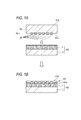
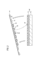
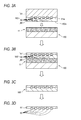
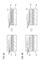


Classifications
-
- C—CHEMISTRY; METALLURGY
- C09—DYES; PAINTS; POLISHES; NATURAL RESINS; ADHESIVES; COMPOSITIONS NOT OTHERWISE PROVIDED FOR; APPLICATIONS OF MATERIALS NOT OTHERWISE PROVIDED FOR
- C09J—ADHESIVES; NON-MECHANICAL ASPECTS OF ADHESIVE PROCESSES IN GENERAL; ADHESIVE PROCESSES NOT PROVIDED FOR ELSEWHERE; USE OF MATERIALS AS ADHESIVES
- C09J7/00—Adhesives in the form of films or foils
- C09J7/10—Adhesives in the form of films or foils without carriers
-
- C—CHEMISTRY; METALLURGY
- C09—DYES; PAINTS; POLISHES; NATURAL RESINS; ADHESIVES; COMPOSITIONS NOT OTHERWISE PROVIDED FOR; APPLICATIONS OF MATERIALS NOT OTHERWISE PROVIDED FOR
- C09J—ADHESIVES; NON-MECHANICAL ASPECTS OF ADHESIVE PROCESSES IN GENERAL; ADHESIVE PROCESSES NOT PROVIDED FOR ELSEWHERE; USE OF MATERIALS AS ADHESIVES
- C09J4/00—Adhesives based on organic non-macromolecular compounds having at least one polymerisable carbon-to-carbon unsaturated bond ; adhesives, based on monomers of macromolecular compounds of groups C09J183/00 - C09J183/16
- C09J4/06—Organic non-macromolecular compounds having at least one polymerisable carbon-to-carbon unsaturated bond in combination with a macromolecular compound other than an unsaturated polymer of groups C09J159/00 - C09J187/00
-
- C—CHEMISTRY; METALLURGY
- C09—DYES; PAINTS; POLISHES; NATURAL RESINS; ADHESIVES; COMPOSITIONS NOT OTHERWISE PROVIDED FOR; APPLICATIONS OF MATERIALS NOT OTHERWISE PROVIDED FOR
- C09J—ADHESIVES; NON-MECHANICAL ASPECTS OF ADHESIVE PROCESSES IN GENERAL; ADHESIVE PROCESSES NOT PROVIDED FOR ELSEWHERE; USE OF MATERIALS AS ADHESIVES
- C09J7/00—Adhesives in the form of films or foils
- C09J7/30—Adhesives in the form of films or foils characterised by the adhesive composition
- C09J7/38—Pressure-sensitive adhesives [PSA]
- C09J7/381—Pressure-sensitive adhesives [PSA] based on macromolecular compounds obtained by reactions involving only carbon-to-carbon unsaturated bonds
- C09J7/385—Acrylic polymers
-
- H—ELECTRICITY
- H01—ELECTRIC ELEMENTS
- H01L—SEMICONDUCTOR DEVICES NOT COVERED BY CLASS H10
- H01L21/00—Processes or apparatus adapted for the manufacture or treatment of semiconductor or solid state devices or of parts thereof
- H01L21/02—Manufacture or treatment of semiconductor devices or of parts thereof
- H01L21/04—Manufacture or treatment of semiconductor devices or of parts thereof the devices having potential barriers, e.g. a PN junction, depletion layer or carrier concentration layer
- H01L21/18—Manufacture or treatment of semiconductor devices or of parts thereof the devices having potential barriers, e.g. a PN junction, depletion layer or carrier concentration layer the devices having semiconductor bodies comprising elements of Group IV of the Periodic Table or AIIIBV compounds with or without impurities, e.g. doping materials
- H01L21/30—Treatment of semiconductor bodies using processes or apparatus not provided for in groups H01L21/20 - H01L21/26
- H01L21/302—Treatment of semiconductor bodies using processes or apparatus not provided for in groups H01L21/20 - H01L21/26 to change their surface-physical characteristics or shape, e.g. etching, polishing, cutting
- H01L21/304—Mechanical treatment, e.g. grinding, polishing, cutting
-
- H—ELECTRICITY
- H01—ELECTRIC ELEMENTS
- H01L—SEMICONDUCTOR DEVICES NOT COVERED BY CLASS H10
- H01L21/00—Processes or apparatus adapted for the manufacture or treatment of semiconductor or solid state devices or of parts thereof
- H01L21/02—Manufacture or treatment of semiconductor devices or of parts thereof
- H01L21/04—Manufacture or treatment of semiconductor devices or of parts thereof the devices having potential barriers, e.g. a PN junction, depletion layer or carrier concentration layer
- H01L21/18—Manufacture or treatment of semiconductor devices or of parts thereof the devices having potential barriers, e.g. a PN junction, depletion layer or carrier concentration layer the devices having semiconductor bodies comprising elements of Group IV of the Periodic Table or AIIIBV compounds with or without impurities, e.g. doping materials
- H01L21/30—Treatment of semiconductor bodies using processes or apparatus not provided for in groups H01L21/20 - H01L21/26
- H01L21/302—Treatment of semiconductor bodies using processes or apparatus not provided for in groups H01L21/20 - H01L21/26 to change their surface-physical characteristics or shape, e.g. etching, polishing, cutting
- H01L21/306—Chemical or electrical treatment, e.g. electrolytic etching
- H01L21/30625—With simultaneous mechanical treatment, e.g. mechanico-chemical polishing
-
- H—ELECTRICITY
- H01—ELECTRIC ELEMENTS
- H01L—SEMICONDUCTOR DEVICES NOT COVERED BY CLASS H10
- H01L21/00—Processes or apparatus adapted for the manufacture or treatment of semiconductor or solid state devices or of parts thereof
- H01L21/02—Manufacture or treatment of semiconductor devices or of parts thereof
- H01L21/04—Manufacture or treatment of semiconductor devices or of parts thereof the devices having potential barriers, e.g. a PN junction, depletion layer or carrier concentration layer
- H01L21/18—Manufacture or treatment of semiconductor devices or of parts thereof the devices having potential barriers, e.g. a PN junction, depletion layer or carrier concentration layer the devices having semiconductor bodies comprising elements of Group IV of the Periodic Table or AIIIBV compounds with or without impurities, e.g. doping materials
- H01L21/30—Treatment of semiconductor bodies using processes or apparatus not provided for in groups H01L21/20 - H01L21/26
- H01L21/31—Treatment of semiconductor bodies using processes or apparatus not provided for in groups H01L21/20 - H01L21/26 to form insulating layers thereon, e.g. for masking or by using photolithographic techniques; After treatment of these layers; Selection of materials for these layers
- H01L21/3105—After-treatment
- H01L21/31058—After-treatment of organic layers
-
- H—ELECTRICITY
- H01—ELECTRIC ELEMENTS
- H01L—SEMICONDUCTOR DEVICES NOT COVERED BY CLASS H10
- H01L21/00—Processes or apparatus adapted for the manufacture or treatment of semiconductor or solid state devices or of parts thereof
- H01L21/02—Manufacture or treatment of semiconductor devices or of parts thereof
- H01L21/04—Manufacture or treatment of semiconductor devices or of parts thereof the devices having potential barriers, e.g. a PN junction, depletion layer or carrier concentration layer
- H01L21/18—Manufacture or treatment of semiconductor devices or of parts thereof the devices having potential barriers, e.g. a PN junction, depletion layer or carrier concentration layer the devices having semiconductor bodies comprising elements of Group IV of the Periodic Table or AIIIBV compounds with or without impurities, e.g. doping materials
- H01L21/30—Treatment of semiconductor bodies using processes or apparatus not provided for in groups H01L21/20 - H01L21/26
- H01L21/31—Treatment of semiconductor bodies using processes or apparatus not provided for in groups H01L21/20 - H01L21/26 to form insulating layers thereon, e.g. for masking or by using photolithographic techniques; After treatment of these layers; Selection of materials for these layers
- H01L21/3105—After-treatment
- H01L21/311—Etching the insulating layers by chemical or physical means
- H01L21/31127—Etching organic layers
- H01L21/31133—Etching organic layers by chemical means
-
- H—ELECTRICITY
- H01—ELECTRIC ELEMENTS
- H01L—SEMICONDUCTOR DEVICES NOT COVERED BY CLASS H10
- H01L21/00—Processes or apparatus adapted for the manufacture or treatment of semiconductor or solid state devices or of parts thereof
- H01L21/67—Apparatus specially adapted for handling semiconductor or electric solid state devices during manufacture or treatment thereof; Apparatus specially adapted for handling wafers during manufacture or treatment of semiconductor or electric solid state devices or components ; Apparatus not specifically provided for elsewhere
- H01L21/683—Apparatus specially adapted for handling semiconductor or electric solid state devices during manufacture or treatment thereof; Apparatus specially adapted for handling wafers during manufacture or treatment of semiconductor or electric solid state devices or components ; Apparatus not specifically provided for elsewhere for supporting or gripping
- H01L21/6835—Apparatus specially adapted for handling semiconductor or electric solid state devices during manufacture or treatment thereof; Apparatus specially adapted for handling wafers during manufacture or treatment of semiconductor or electric solid state devices or components ; Apparatus not specifically provided for elsewhere for supporting or gripping using temporarily an auxiliary support
- H01L21/6836—Wafer tapes, e.g. grinding or dicing support tapes
-
- C—CHEMISTRY; METALLURGY
- C08—ORGANIC MACROMOLECULAR COMPOUNDS; THEIR PREPARATION OR CHEMICAL WORKING-UP; COMPOSITIONS BASED THEREON
- C08F—MACROMOLECULAR COMPOUNDS OBTAINED BY REACTIONS ONLY INVOLVING CARBON-TO-CARBON UNSATURATED BONDS
- C08F222/00—Copolymers of compounds having one or more unsaturated aliphatic radicals, each having only one carbon-to-carbon double bond, and at least one being terminated by a carboxyl radical and containing at least one other carboxyl radical in the molecule; Salts, anhydrides, esters, amides, imides, or nitriles thereof
- C08F222/10—Esters
-
- C—CHEMISTRY; METALLURGY
- C09—DYES; PAINTS; POLISHES; NATURAL RESINS; ADHESIVES; COMPOSITIONS NOT OTHERWISE PROVIDED FOR; APPLICATIONS OF MATERIALS NOT OTHERWISE PROVIDED FOR
- C09J—ADHESIVES; NON-MECHANICAL ASPECTS OF ADHESIVE PROCESSES IN GENERAL; ADHESIVE PROCESSES NOT PROVIDED FOR ELSEWHERE; USE OF MATERIALS AS ADHESIVES
- C09J133/00—Adhesives based on homopolymers or copolymers of compounds having one or more unsaturated aliphatic radicals, each having only one carbon-to-carbon double bond, and at least one being terminated by only one carboxyl radical, or of salts, anhydrides, esters, amides, imides, or nitriles thereof; Adhesives based on derivatives of such polymers
- C09J133/04—Homopolymers or copolymers of esters
- C09J133/06—Homopolymers or copolymers of esters of esters containing only carbon, hydrogen and oxygen, the oxygen atom being present only as part of the carboxyl radical
-
- C—CHEMISTRY; METALLURGY
- C09—DYES; PAINTS; POLISHES; NATURAL RESINS; ADHESIVES; COMPOSITIONS NOT OTHERWISE PROVIDED FOR; APPLICATIONS OF MATERIALS NOT OTHERWISE PROVIDED FOR
- C09J—ADHESIVES; NON-MECHANICAL ASPECTS OF ADHESIVE PROCESSES IN GENERAL; ADHESIVE PROCESSES NOT PROVIDED FOR ELSEWHERE; USE OF MATERIALS AS ADHESIVES
- C09J2203/00—Applications of adhesives in processes or use of adhesives in the form of films or foils
- C09J2203/326—Applications of adhesives in processes or use of adhesives in the form of films or foils for bonding electronic components such as wafers, chips or semiconductors
-
- C—CHEMISTRY; METALLURGY
- C09—DYES; PAINTS; POLISHES; NATURAL RESINS; ADHESIVES; COMPOSITIONS NOT OTHERWISE PROVIDED FOR; APPLICATIONS OF MATERIALS NOT OTHERWISE PROVIDED FOR
- C09J—ADHESIVES; NON-MECHANICAL ASPECTS OF ADHESIVE PROCESSES IN GENERAL; ADHESIVE PROCESSES NOT PROVIDED FOR ELSEWHERE; USE OF MATERIALS AS ADHESIVES
- C09J2400/00—Presence of inorganic and organic materials
- C09J2400/20—Presence of organic materials
- C09J2400/22—Presence of unspecified polymer
-
- C—CHEMISTRY; METALLURGY
- C09—DYES; PAINTS; POLISHES; NATURAL RESINS; ADHESIVES; COMPOSITIONS NOT OTHERWISE PROVIDED FOR; APPLICATIONS OF MATERIALS NOT OTHERWISE PROVIDED FOR
- C09J—ADHESIVES; NON-MECHANICAL ASPECTS OF ADHESIVE PROCESSES IN GENERAL; ADHESIVE PROCESSES NOT PROVIDED FOR ELSEWHERE; USE OF MATERIALS AS ADHESIVES
- C09J2433/00—Presence of (meth)acrylic polymer
-
- H—ELECTRICITY
- H01—ELECTRIC ELEMENTS
- H01L—SEMICONDUCTOR DEVICES NOT COVERED BY CLASS H10
- H01L2221/00—Processes or apparatus adapted for the manufacture or treatment of semiconductor or solid state devices or of parts thereof covered by H01L21/00
- H01L2221/67—Apparatus for handling semiconductor or electric solid state devices during manufacture or treatment thereof; Apparatus for handling wafers during manufacture or treatment of semiconductor or electric solid state devices or components; Apparatus not specifically provided for elsewhere
- H01L2221/683—Apparatus for handling semiconductor or electric solid state devices during manufacture or treatment thereof; Apparatus for handling wafers during manufacture or treatment of semiconductor or electric solid state devices or components; Apparatus not specifically provided for elsewhere for supporting or gripping
- H01L2221/68304—Apparatus for handling semiconductor or electric solid state devices during manufacture or treatment thereof; Apparatus for handling wafers during manufacture or treatment of semiconductor or electric solid state devices or components; Apparatus not specifically provided for elsewhere for supporting or gripping using temporarily an auxiliary support
- H01L2221/68318—Auxiliary support including means facilitating the separation of a device or wafer from the auxiliary support
-
- H—ELECTRICITY
- H01—ELECTRIC ELEMENTS
- H01L—SEMICONDUCTOR DEVICES NOT COVERED BY CLASS H10
- H01L2221/00—Processes or apparatus adapted for the manufacture or treatment of semiconductor or solid state devices or of parts thereof covered by H01L21/00
- H01L2221/67—Apparatus for handling semiconductor or electric solid state devices during manufacture or treatment thereof; Apparatus for handling wafers during manufacture or treatment of semiconductor or electric solid state devices or components; Apparatus not specifically provided for elsewhere
- H01L2221/683—Apparatus for handling semiconductor or electric solid state devices during manufacture or treatment thereof; Apparatus for handling wafers during manufacture or treatment of semiconductor or electric solid state devices or components; Apparatus not specifically provided for elsewhere for supporting or gripping
- H01L2221/68304—Apparatus for handling semiconductor or electric solid state devices during manufacture or treatment thereof; Apparatus for handling wafers during manufacture or treatment of semiconductor or electric solid state devices or components; Apparatus not specifically provided for elsewhere for supporting or gripping using temporarily an auxiliary support
- H01L2221/68327—Apparatus for handling semiconductor or electric solid state devices during manufacture or treatment thereof; Apparatus for handling wafers during manufacture or treatment of semiconductor or electric solid state devices or components; Apparatus not specifically provided for elsewhere for supporting or gripping using temporarily an auxiliary support used during dicing or grinding
-
- H—ELECTRICITY
- H01—ELECTRIC ELEMENTS
- H01L—SEMICONDUCTOR DEVICES NOT COVERED BY CLASS H10
- H01L2221/00—Processes or apparatus adapted for the manufacture or treatment of semiconductor or solid state devices or of parts thereof covered by H01L21/00
- H01L2221/67—Apparatus for handling semiconductor or electric solid state devices during manufacture or treatment thereof; Apparatus for handling wafers during manufacture or treatment of semiconductor or electric solid state devices or components; Apparatus not specifically provided for elsewhere
- H01L2221/683—Apparatus for handling semiconductor or electric solid state devices during manufacture or treatment thereof; Apparatus for handling wafers during manufacture or treatment of semiconductor or electric solid state devices or components; Apparatus not specifically provided for elsewhere for supporting or gripping
- H01L2221/68304—Apparatus for handling semiconductor or electric solid state devices during manufacture or treatment thereof; Apparatus for handling wafers during manufacture or treatment of semiconductor or electric solid state devices or components; Apparatus not specifically provided for elsewhere for supporting or gripping using temporarily an auxiliary support
- H01L2221/6834—Apparatus for handling semiconductor or electric solid state devices during manufacture or treatment thereof; Apparatus for handling wafers during manufacture or treatment of semiconductor or electric solid state devices or components; Apparatus not specifically provided for elsewhere for supporting or gripping using temporarily an auxiliary support used to protect an active side of a device or wafer
-
- H—ELECTRICITY
- H01—ELECTRIC ELEMENTS
- H01L—SEMICONDUCTOR DEVICES NOT COVERED BY CLASS H10
- H01L2221/00—Processes or apparatus adapted for the manufacture or treatment of semiconductor or solid state devices or of parts thereof covered by H01L21/00
- H01L2221/67—Apparatus for handling semiconductor or electric solid state devices during manufacture or treatment thereof; Apparatus for handling wafers during manufacture or treatment of semiconductor or electric solid state devices or components; Apparatus not specifically provided for elsewhere
- H01L2221/683—Apparatus for handling semiconductor or electric solid state devices during manufacture or treatment thereof; Apparatus for handling wafers during manufacture or treatment of semiconductor or electric solid state devices or components; Apparatus not specifically provided for elsewhere for supporting or gripping
- H01L2221/68304—Apparatus for handling semiconductor or electric solid state devices during manufacture or treatment thereof; Apparatus for handling wafers during manufacture or treatment of semiconductor or electric solid state devices or components; Apparatus not specifically provided for elsewhere for supporting or gripping using temporarily an auxiliary support
- H01L2221/68381—Details of chemical or physical process used for separating the auxiliary support from a device or wafer
Definitions
- the present invention relates to a temporary adhesive for producing a semiconductor device, an adhesive support using the same, and a method for producing a semiconductor device.
- a wire bonding method has conventionally been widely known as an electrical connection method from an integrated circuit in an IC chip to an external terminal of the IC chip
- a silicon substrate has recently been used to achieve miniaturization of the IC chip.
- a method so-called method of forming a silicon through electrode (TSV)
- TSV silicon through electrode
- the method of forming the through silicon via alone can not sufficiently meet the above-mentioned recent need for higher integration of the IC chip.
- a semiconductor silicon wafer having a thickness of about 700 to 900 ⁇ m is widely known as a semiconductor silicon wafer used in a process of manufacturing a semiconductor device. It has been attempted to reduce the thickness to 200 .mu.m or less. However, since semiconductor silicon wafers having a thickness of 200 ⁇ m or less are very thin and, consequently, members for manufacturing semiconductor devices based on them are also very thin, such members may be further processed or In the case of simply moving such a member, it is difficult to support the member stably and without damage.
- a semiconductor wafer before thinning on which a device is provided on the surface and a processing supporting substrate are temporarily bonded with a silicone adhesive, and the back surface of the semiconductor wafer is ground and thinned There is known a technique in which a semiconductor wafer is perforated to form a silicon through electrode, and thereafter, a processing support substrate is detached from the semiconductor wafer (see Patent Document 1). According to this technology, resistance to grinding during backside grinding of semiconductor wafers, heat resistance in anisotropic dry etching processes, etc., chemical resistance during plating and etching, and smooth peeling from the final support substrate for processing It is believed that low adherent contamination can be achieved simultaneously.
- a method of supporting a wafer is a method of supporting a wafer by a support layer system, in which a plasma polymer layer obtained by a plasma deposition method is interposed as a separation layer between the wafer and the support layer system.
- the adhesive bond between the support layer system and the release layer is made greater than the bond bond between the wafer and the release layer, and the wafer is easily released from the release layer when the wafer is released from the support layer system.
- Patent Document 2 There is also known a technology configured to separate.
- a pressure-sensitive adhesive film which is composed of syndiotactic 1,2-polybutadiene and a photopolymerization initiator and whose adhesive force is changed by irradiation of radiation (see Patent Document 6). Further, the supporting substrate and the semiconductor wafer are temporarily bonded with an adhesive made of polycarbonates, and the semiconductor wafer is treated, then irradiated with irradiation radiation, and then heated to thereby process the treated semiconductor wafer. There is known a technique for detaching the support substrate from the support substrate (see Patent Document 7).
- a pressure-sensitive adhesive composition comprising an energy ray-curable copolymer having an energy ray-polymerizable unsaturated group in a side chain, an epoxy resin, and a heat-activated latent epoxy resin curing agent.
- a pressure-sensitive adhesive tape which is made of a pressure-sensitive adhesive layer and whose adhesive force changes upon irradiation with radiation (see Patent Document 8). Similar techniques include an acrylic polymer having a weight average molecular weight of 30,000 to 2,000,000 and having an unsaturated hydrocarbon group, an epoxy-based thermosetting resin having an unsaturated hydrocarbon group, and a thermosetting agent. Adhesive compositions are also known (see Patent Document 9).
- the surface of the semiconductor wafer on which the device is provided (that is, the device surface of the device wafer) and the supporting substrate (carrier substrate) are temporarily adhered via a layer made of an adhesive known in Patent Document 1 and the like.
- the adhesive layer is required to have a certain degree of adhesion in order to stably support the semiconductor wafer. Therefore, in the case where the entire surface of the device surface of the semiconductor wafer and the supporting substrate are temporarily bonded via the adhesive layer, the temporary bonding between the semiconductor wafer and the supporting substrate is made sufficient, and the semiconductor wafer is stabilized stably.
- the temporary adhesion between the semiconductor wafer and the support substrate is too strong to support the substrate without damaging it, so that the device may be damaged when the semiconductor wafer is detached from the support substrate, or from the semiconductor wafer It is easy for the problem that the device is detached.
- the plasma polymer layer as the separation layer is interposed between the wafer and the support layer system by plasma deposition.
- the formation method is (1) usually, the equipment cost for carrying out plasma deposition is large; (2) layer formation by plasma deposition requires time for vacuuming in the plasma apparatus and deposition of monomers; (3) Even when a separation layer comprising a plasma polymer layer is provided, when supporting a wafer to be processed, the support of the wafer is released while securing sufficient adhesive bonding between the wafer and the separation layer. In such cases, it is not easy to control an adhesive bond such that the wafer is easily detached from the separation layer;
- the present invention has been made in view of the above background, and an object of the present invention is to temporarily support a member to be treated with high adhesion when subjecting a member to be treated (such as a semiconductor wafer) to mechanical or chemical treatment. And a temporary adhesive for manufacturing a semiconductor device which can be easily (with high releasability) releasing temporary support to the treated member without damaging the treated member, and adhesion using the same.
- a support and a method of manufacturing a semiconductor device are provided.
- the inventors of the present invention have made intensive studies to solve the above problems, and the reason is not clear, but (A) a polymer compound having a radical polymerizable group in the side chain, (B) a radical polymerizable monomer, and When a composition containing a thermal radical polymerization initiator (C) is used as a temporary adhesive in the temporary bonding step between the semiconductor wafer and the support substrate, the member to be treated can be temporarily supported with high adhesive strength, and After the treatment of the member, the adhesive layer is brought into contact with the peeling solvent, so that heating, irradiation with an actinic ray or radiation as in the prior art described above is not performed, and the treated member is treated. It has been found that temporary support can be easily released, and the present invention has been completed. That is, the present invention is as follows.
- the temporary adhesive for semiconductor device manufacture which contains the high molecular compound which has a radically polymerizable group in (A) side chain, (B) radically polymerizable monomer, and (C) thermal radical polymerization initiator.
- the polymer compound (A) is represented by the group represented by the following general formula (1), the group represented by the following general formula (2), and the following general formula (3) as the radical polymerizable group
- the temporary adhesive for semiconductor device manufacture as described in said [1] which has 1 or more types of groups chosen from the group which consists of. (Wherein, X and Y each independently represent an oxygen atom, a sulfur atom or -N (R 12 )-.
- Z represents an oxygen atom, a sulfur atom, -N (R 12 )-or a phenylene group.
- R 1 to R 12 each independently represent a hydrogen atom or a monovalent substituent.
- An adhesive support comprising a substrate and an adhesive layer formed on the substrate by the temporary adhesive for producing a semiconductor device according to any one of the above [1] to [8].
- the surface of the adhesive layer to be adhered to the first surface of the member to be treated A method of manufacturing a semiconductor device according to the above [10], further comprising the step of irradiating the actinic ray or radiation or heat.
- the semiconductor according to the above [10] or [11] further comprising the step of heating the adhesive layer at a temperature of 50 ° C. to 300 ° C. prior to the step of chemically treating or obtaining a treated member Device manufacturing method.
- the process according to any one of the above [10] to [12], wherein the step of detaching the first surface of the treated member from the adhesive layer includes the step of bringing a peeling solution into contact with the adhesive layer.
- Semiconductor device manufacturing method [14]
- the to-be-treated member has a to-be-treated substrate, and a protective layer provided on the first surface of the to-be-treated substrate, The surface of the protective layer opposite to the substrate to be treated is taken as the first surface of the member to be treated,
- the semiconductor according to any one of the above [10] to [13], wherein a second surface different from the first surface of the substrate to be treated is the second surface of the member to be treated Device manufacturing method.
- the present invention when mechanical or chemical treatment is performed on a member to be treated, it is possible to temporarily support the member to be treated with high adhesive force, and to temporarily treat the treated member without damaging the treated member.
- the temporary adhesive for semiconductor device manufacture which can release a support, the adhesive support using the same, and the manufacturing method of a semiconductor device can be provided.
- FIGS. 1A and 1B are schematic cross-sectional views illustrating temporary bonding between an adhesive support and a device wafer, and a schematic cross-sectional view showing a thinned state of a device wafer temporarily bonded by an adhesive support.
- FIG. It is a schematic sectional drawing explaining cancellation
- FIGS. 3A, 3B, 3C, and 3D are schematic cross-sectional views for explaining temporary adhesion between an adhesive support and a device wafer with a protective layer, respectively, a device wafer with a protective layer temporarily adhered by an adhesive support.
- FIG. 1 is a schematic sectional view showing a thinned state, a schematic sectional view showing a thin device wafer with a protective layer peeled from an adhesive support, and a schematic sectional view showing a thin device wafer.
- FIGS. 4A and 4B are schematic cross-sectional views illustrating the thinned state of the device wafer temporarily bonded by the adhesive support, and the device wafer with protective layer temporarily bonded by the adhesive support. It is a schematic sectional drawing explaining the state by which it was thinned.
- FIG. 5A shows a schematic cross-sectional view illustrating exposure to an adhesive support
- FIG. 5B shows a schematic top view of the mask.
- FIG. 6A shows a schematic cross-sectional view of the pattern-exposed adhesive support
- FIG. 6B shows a schematic top view of the pattern-exposed adhesive support.
- FIG. 2 shows a schematic cross-sectional view illustrating irradiation of an adhesive support with actinic rays or radiation or heat.
- the notations not describing substitution and non-substitution include those having no substituent and those having a substituent.
- the "alkyl group” includes not only an alkyl group having no substituent (unsubstituted alkyl group) but also an alkyl group having a substituent (substituted alkyl group).
- active light or “radiation” means, for example, visible light, ultraviolet light, far ultraviolet light, electron beam, X-ray and the like.
- light means actinic rays or radiation.
- the "exposure” in the present specification means not only exposure by a mercury lamp, ultraviolet rays, far ultraviolet rays represented by an excimer laser, X-rays, EUV light, etc., but also electron beams and ion beams. It also means drawing by particle beam.
- “(meth) acrylate” represents acrylate and methacrylate
- “(meth) acrylic represents acrylic and methacrylic
- a polymerizable compound is a compound having a polymerizable group, and may be a monomer or a polymer.
- the polymerizable group is a group involved in a polymerization reaction. say.
- the temporary adhesive for semiconductor device production of the present invention (hereinafter, also simply referred to as “temporary adhesive”) is (A) a polymer compound having a radically polymerizable group in the side chain, (B) a radically polymerizable monomer, and , (C) contains a thermal radical polymerization initiator.
- temporary adhesive for manufacturing a semiconductor device of the present invention when mechanical or chemical treatment is performed on a member to be treated, the member to be treated can be temporarily supported with high adhesive force, and damage to the treated member is caused. As a result, a temporary adhesive for semiconductor device manufacture can be obtained which can release temporary support for the processed member. It is preferable that the temporary adhesive for semiconductor device manufacture of this invention is for silicon penetration electrode formation. The formation of the through silicon via will be described in detail later.
- a (meth) acrylic polymer, a styrene polymer, a polyurethane resin, a polyvinyl alcohol resin, a polyvinyl acetal resin (preferably, Polyvinyl butyral resin), polyvinyl formal resin, polyamide resin, polyester resin, epoxy resin, novolac resin, etc. can be used, and it has a radically polymerizable group in the side chain of a polymer.
- the polymer compound (A) is generally synthesized by polymerizing a monomer having a partial structure to be polymerized by radical polymerization or the like, and has a repeating unit derived from a monomer having a partial structure to be polymerized.
- a partial structure to be polymerized for example, an ethylenic polymerizable partial structure can be mentioned.
- (meth) acrylic polymers and polyurethane resins can be preferably used.
- the radically polymerizable group that the polymer compound (A) has is a group that can be polymerized by the action of a radical.
- the adhesive support is adhered to the member to be treated and then heat treatment is performed, whereby the polymerization reaction further proceeds by the radicals generated from the thermal radical polymerization initiator,
- the to-be-processed member can be temporarily supported by high adhesive force.
- a polymerization reaction occurs in the exposed area.
- the adhesive layer can be provided with areas of high and low adhesion.
- the adhesive layer of the adhesive support is irradiated with an actinic ray, radiation or heat to form a radical polymerizable group of the polymer compound.
- a polymerization reaction can be carried out to form an adhesive layer with reduced adhesion from the inner surface to the outer surface of the substrate side. That is, the adhesion between the substrate and the adhesive layer in the adhesive support can be made high while the adhesion of the adhesive layer to the member to be treated can be lowered.
- the radically polymerizable group is preferably, for example, a functional group capable of undergoing an addition polymerization reaction, and examples of the functional group capable of undergoing an addition polymerization reaction include an ethylenically unsaturated group.
- the ethylenic unsaturated bond group is preferably a styryl group, an allyl group, a (meth) acryloyl group, a vinyl group, a vinyloxy group or an alkynyl group.
- free radicals polymerization initiating radicals or propagating radicals in the polymerization process of the polymerizable compound
- polymer chains of polymer compounds directly or polymerization chains of polymerizable monomers are added.
- atoms of the polymer compound for example, a hydrogen atom on a carbon atom adjacent to a functional crosslinking group
- Crosslinks are formed between them to cure.
- the polymer compound (A) is, as a radically polymerizable group, a group represented by the following general formula (1), a group represented by the following general formula (2), and the following general formula (3) It is preferable to have 1 or more types of groups chosen from the group which consists of a group represented by, and it is more preferable to have a group represented by following General formula (1).
- X and Y each independently represent an oxygen atom, a sulfur atom or -N (R 12 )-.
- Z represents an oxygen atom, a sulfur atom, -N (R 12 )-or a phenylene group.
- R 1 to R 12 each independently represent a hydrogen atom or a monovalent substituent.
- R 1 to R 3 each independently represent a hydrogen atom or a monovalent substituent, and for example, R 1 is a hydrogen atom or a monovalent organic group, for example, having a substituent.
- the alkyl group etc. which may be mentioned are mentioned, Especially, a hydrogen atom, a methyl group, a methyl alkoxy group, and a methyl ester group are preferable.
- R 2 and R 3 may each independently have a hydrogen atom, a halogen atom, an amino group, a dialkylamino group, a carboxyl group, an alkoxycarbonyl group, a sulfo group, a nitro group, a cyano group or a substituent Alkyl group, aryl group which may have a substituent, alkoxy group which may have a substituent, aryloxy group which may have a substituent, alkylamino group which may have a substituent, substitution Arylamino group which may have a group, alkylsulfonyl group which may have a substituent, arylsulfonyl group which may have a substituent, etc., among which hydrogen atom, carboxyl group, alkoxycarbonyl group It is preferably an alkyl group which may have a substituent or an aryl group which may have a substituent.
- examples of the substituent which can be introduced include a methoxycarbonyl group, an ethoxycarbonyl group, an isopropyloxycarbonyl group, a methyl group, an ethyl group, a phenyl group and the like.
- X represents an oxygen atom, a sulfur atom, or -N (R 12 )-, and R 12 includes a hydrogen atom, an alkyl group which may have a substituent, and the like.
- R 4 to R 8 each independently represent a hydrogen atom or a monovalent substituent, and for example, a hydrogen atom, a halogen atom, an amino group, a dialkylamino group, a carboxyl group, an alkoxycarbonyl group A sulfo group, a nitro group, a cyano group, an alkyl group which may have a substituent, an aryl group which may have a substituent, an alkoxy group which may have a substituent, and a substituent An aryloxy group, an alkylamino group which may have a substituent, an arylamino group which may have a substituent, an alkylsulfonyl group which may have a substituent, and a substituent Among them, a hydrogen atom, a carboxyl group, an alkoxycarbonyl group, an alkyl group which may have a substituent, and an aryl group which may have a substituent are preferable.
- R 9 to R 11 each independently represent a hydrogen atom or a monovalent substituent, and examples thereof include a hydrogen atom, a halogen atom, an amino group, a dialkylamino group, a carboxyl group, and an alkoxycarbonyl group.
- a sulfo group, a nitro group, a cyano group, an alkyl group which may have a substituent, an aryl group which may have a substituent, an alkoxy group which may have a substituent, and a substituent An aryloxy group, an alkylamino group which may have a substituent, an arylamino group which may have a substituent, an alkylsulfonyl group which may have a substituent, and a substituent And arylsulfonyl groups and the like, and among them, a hydrogen atom, a carboxyl group, an alkoxycarbonyl group, an alkyl group which may have a substituent, and an aryl group which may have a substituent are preferable.
- Z represents an oxygen atom, a sulfur atom, -N (R 12 )-or a phenylene group.
- R 12 those mentioned in the general formula (1) can be mentioned.
- a radically polymerizable group having a methacryloyl group represented by the general formula (1) is preferable.
- the content thereof is iodine titration (1 g of the polymer compound (A) Measurement of the content of the radically polymerizable group) is preferably 0.1 to 10.0 mmol, more preferably 1.0 to 7.0 mmol, and most preferably 2.0 to 5.5 mmol. Within this range, good sensitivity and good storage stability can be obtained.
- the polymer compound (A) typically has a repeating unit having a radically polymerizable group, and in that case, the content of the repeating unit having a radically polymerizable group is the same as that of the polymer compound (A)
- the amount is preferably 1 to 70 mol%, more preferably 2 to 60 mol%, and still more preferably 5 to 50 mol%, based on all repeating units of
- the radically polymerizable group includes (a) urethanization reaction using a hydroxy group of a polymer side chain and an isocyanate having a radical polymerization reactive group, (b) a hydroxy group of a polymer side chain and a radical polymerization reactive group Esterification reaction with carboxylic acid, carboxylic acid halide, sulfonic acid halide, or carboxylic acid anhydride, (c) Carboxy group of polymer side chain or salt thereof and isocyanate having radically polymerizable reactive group Reaction, (d) Esterification reaction using a halogenated carbonyl group of a polymer side chain, a carboxy group or a salt thereof, and an alcohol having a radical polymerization reactive group, (e) A halogenated carbonyl group of a polymer side chain, Carboxy Amidation reaction using a group or a salt thereof and an amine having a radical polymerization reactive group, (f) a polymer Amidation reaction using a chain
- the polymer compound (A) preferably has a repeating unit having at least one of the groups represented by the general formulas (1) to (3) described above. Specifically as such a repeating unit, the repeating unit represented by the following general formula (4) is more preferable.
- R 101 to R 103 each independently represent a hydrogen atom, an alkyl group having 1 to 6 carbon atoms, or a halogen atom.
- T represents a radically polymerizable group represented by any of the above general formulas (1) to (3), and preferred embodiments are also the same as those described for the radically polymerizable group described above.
- A is selected from the group consisting of a single bond, or -CO-, -O-, -NH-, a divalent aliphatic group, a divalent aromatic group and a combination thereof Represents a divalent linking group.
- L 1 to L 18 of A consisting of combinations are listed below.
- the left side is bonded to the main chain, and the right side is bonded to the radical polymerizable group represented by any one of the general formulas (1) to (3).
- L 1 —CO—NH 2 divalent aliphatic group —O—CO—NH 2 divalent aliphatic group— L 2 : —CO—NH2 divalent aliphatic group— L 3 : -CO-divalent aliphatic group- L 4 : -CO-O-divalent aliphatic group- L 5 : -divalent aliphatic group- L 6 : —CO—NH 2 divalent aromatic group— L 7 : -CO-divalent aromatic group- L 8 : -divalent aromatic group- L 9 : —CO—O-divalent aliphatic group —CO—O-divalent aliphatic group— L 10 : —CO—O-divalent aliphatic group —O—CO-divalent aliphatic group— L 11 : -CO-O-divalent aromatic group -CO-O-divalent aliphatic group- L 12 : -CO-O-divalent aromatic group
- the divalent aliphatic group means an alkylene group, a substituted alkylene group, an alkenylene group, a substituted alkenylene group, an alkynylene group, a substituted alkynylene group or a polyalkyleneoxy group.
- an alkylene group, a substituted alkylene group, an alkenylene group and a substituted alkenylene group are preferable, and an alkylene group and a substituted alkylene group are more preferable.
- a chain structure is more preferable than a cyclic structure, and a linear structure is more preferable than a chain structure having a branch.
- the carbon atom number of the divalent aliphatic group is preferably 1 to 20, more preferably 1 to 15, still more preferably 1 to 12, and still more preferably 1 to 10.
- the number is preferably 1 to 8, more preferably 1 to 8, and particularly preferably 1 to 4.
- substituent of the divalent aliphatic group include a halogen atom (F, Cl, Br, I), a hydroxy group, a carboxy group, an amino group, a cyano group, an aryl group, an alkoxy group, an aryloxy group, an acyl group And alkoxycarbonyl group, aryloxycarbonyl group, acyloxy group, monoalkylamino group, dialkylamino group, arylamino group and diarylamino group.
- divalent aromatic groups examples include phenylene, substituted phenylene, naphthalene and substituted naphthalene, with phenylene being preferred.
- substituent of a bivalent aromatic group in addition to the example of the substituent of the said bivalent aliphatic group, an alkyl group is mentioned.
- the polymer compound (A) preferably has another repeating unit in addition to the repeating unit having a radically polymerizable group, as long as the effects of the present invention are not impaired, for the purpose of improving various properties such as adhesive strength. .
- a polymer compound that can be synthesized by radical polymerization such as a (meth) acrylic polymer
- a monomer which can be copolymerized for example, acrylic acid esters, methacrylic acid esters, N, N 2-substituted acrylamides, N, N 2-substituted methacrylamides, styrenes, acrylonitriles, methacrylonitrile And monomers selected from the class and the like.
- acrylic esters such as alkyl acrylate (the alkyl group preferably has 1 to 20 carbon atoms) and the like (specifically, for example, methyl acrylate, ethyl acrylate, acrylic) Propyl acrylate, butyl acrylate, amyl acrylate, ethyl hexyl acrylate, octyl acrylate, t-octyl acrylate, chloroethyl acrylate, 2,2-dimethylhydroxypropyl acrylate, 5-hydroxypentyl acrylate, trimethylolpropane monoacrylate , Pentaerynuritol monoacrylate, glycidyl acrylate, benzyl acrylate, methoxybenzyl acrylate, furfuryl acrylate, tetrahydrofurfuryl acrylate etc., aryl acrylates (eg, Methacrylic acid esters such as phenyl acrylate and the alkyl acryl
- styrene eg methyl styrene, dimethyl styrene, trimethyl styrene, ethyl styrene, diethyl styrene, isopropyl styrene
- the polymer compound (A) is preferably substantially insoluble in an alkali solution from the viewpoint of resistance to an alkali solution which may come in contact with the semiconductor device during production of the semiconductor device.
- substantially insoluble in an alkali solution means that only the polymer compound (A) is dissolved in a solvent such as butyl acetate to apply a composition having a solid content concentration of 3.5% by mass on a silicon wafer.
- TMAH tetramethylammonium hydroxide
- the polymer compound (A) is preferably substantially insoluble in alkali
- the polymer compound (A) may or may not have an acid group, but does not have it. Is preferred.
- Examples of the acid group include a carboxyl group, a sulfonamide group, a sulfonylimide group, a bissulfonylimide group, and an aliphatic alcohol in which the ⁇ -position is substituted with an electron-withdrawing group (eg, hexafluoroisopropanol group, —C (CF 3 )) 2 OH) etc.
- an electron-withdrawing group eg, hexafluoroisopropanol group, —C (CF 3 )
- the polymer compound (A) When the polymer compound (A) has an acid group, the polymer compound (A) preferably has a repeating unit having an acid group, in which case, the inclusion of the repeating unit having an acid group in the polymer compound (A) 25 mol% or less is preferable, 15 mol% or less is more preferable, and 10 mol% or less is more preferable.
- the content of the repeating unit having an acid group in the polymer compound (A) is usually 1 mol% or more.
- the electron withdrawing group is a substituent having a tendency to attract an electron, and for example, a substituent having a tendency to attract an electron from an atom in a position close to the group in the molecule.
- the mass average molecular weight (Mw) of the polymer compound (A) is preferably 2,500 or more, more preferably 2,500 to 1,000,000, and more preferably 5,000 to 1,000, in terms of polystyrene equivalent by GPC method. , 000 is more preferable.
- the degree of dispersion (mass average molecular weight / number average molecular weight) of the polymer compound (A) is preferably 1.1 to 10.
- GPC method uses HLC-8020GPC (made by Tosoh Corp.), TSKgel SuperHZM-H, TSKgel SuperHZ4000, TSKgel SuperHZ 2000 (made by Tosoh Corp., 4.6 mm ID ⁇ 15 cm) as columns, THF (tetrahydrofuran as the eluent) Based on the method using
- the polymer compound (A) may be used in combination of two or more as needed.
- the content of the polymer compound (A) is preferably 5 to 95% by mass, and more preferably 10 to 90% by mass, with respect to the total solid content of the temporary adhesive for producing a semiconductor device, from the viewpoint of good adhesive strength. 20 to 80% by mass is more preferable.
- compositional ratio of the polymer structure represents a mole percentage.
- the temporary adhesive for producing a semiconductor device of the present invention contains a radically polymerizable monomer.
- the radically polymerizable monomer typically has a radically polymerizable group.
- a radically polymerizable group is a group which can be polymerized by the action of a radical.
- the radically polymerizable monomer is a compound different from the above-described polymer compound (A).
- the polymerizable monomer is typically a low molecular weight compound, preferably a low molecular weight compound having a molecular weight of 2000 or less, more preferably a low molecular weight compound having a molecular weight of 1500 or less, and a low molecular weight compound having a molecular weight of 900 or less. It is further preferred that The molecular weight is usually 100 or more.
- the polymerizable monomer in the exposed area is subjected to pattern exposure to the adhesive layer in the adhesive support before the adhesive support is adhered to the treated member.
- the polymerization reaction can be performed to provide the adhesive layer with a high adhesive area and a low adhesive area.
- the adhesive layer of the adhesive support is irradiated with an actinic ray, radiation or heat to perform the polymerization reaction by the radical polymerizable monomer. Can form an adhesive layer with reduced adhesion from the inner surface to the outer surface on the substrate side. That is, the adhesion between the substrate and the adhesive layer in the adhesive support can be made high while the adhesion of the adhesive layer to the member to be treated can be lowered.
- the radically polymerizable monomer is selected from compounds having at least one, preferably two or more radically polymerizable groups.
- Such compounds are widely known in the relevant industrial field, and they can be used in the present invention without particular limitation. These may be, for example, any of chemical forms such as monomers, prepolymers, that is, dimers, trimers and oligomers, or mixtures thereof and multimers thereof.
- the radically polymerizable monomers in the present invention may be used singly or in combination of two or more.
- the radically polymerizable group is preferably an ethylenically unsaturated group.
- the ethylenically unsaturated group is preferably a styryl group, a (meth) acryloyl group or an allyl group.
- examples of monomers and prepolymers thereof include unsaturated carboxylic acids (eg, acrylic acid, methacrylic acid, itaconic acid, crotonic acid, isocrotonic acid, maleic acid etc.) and esters thereof, amides, etc. And multimers thereof, and preferably esters of unsaturated carboxylic acids and polyhydric alcohol compounds, and amides of unsaturated carboxylic acids and polyhydric amine compounds, and multimers thereof. Also, addition reaction products of unsaturated carboxylic acid esters or amides having a nucleophilic substituent such as hydroxyl group, amino group, mercapto group etc.
- unsaturated carboxylic acids eg, acrylic acid, methacrylic acid, itaconic acid, crotonic acid, isocrotonic acid, maleic acid etc.
- esters thereof eg. acrylic acid, methacrylic acid, itaconic acid, crotonic acid, isocrotonic acid, maleic acid etc.
- unsaturated carboxylic acid instead of the above unsaturated carboxylic acid, it is also possible to use unsaturated phosphonic acid, a vinyl benzene derivative such as styrene, a vinyl ether, an allyl ether or the like, and a group of compounds replaced.
- unsaturated phosphonic acid a vinyl benzene derivative such as styrene, a vinyl ether, an allyl ether or the like, and a group of compounds replaced.
- ester monomer of polyhydric alcohol compound and unsaturated carboxylic acid examples include ethylene glycol diacrylate, triethylene glycol diacrylate, 1,3-butanediol diacrylate and tetramethylene glycol diacrylate as acrylic acid ester.
- tetramethylene glycol dimethacrylate triethylene glycol dimethacrylate, neopentyl glycol dimethacrylate, trimethylolpropane trimethacrylate, trimethylolethane trimethacrylate, ethylene glycol dimethacrylate, 1,3-butanediol dimethacrylate, Hexanediol dimethacrylate, pentaerythritol dimethacrylate, pentaerythritol trimethacrylate, pentaerythritol tetramethacrylate, dipentaerythritol dimethacrylate, dipentaerythritol hexamethacrylate, sorbitol trimethacrylate, sorbitol tetramethacrylate, bis [p- (3-methacryloxy-) 2-hydroxy group Epoxy) phenyl] dimethyl methane, bis - [p- (
- ethylene glycol diitaconate propylene glycol diitaconate, 1,3-butanediol diitaconate, 1,4-butanediol diitaconate, tetramethylene glycol diitaconate, pentaerythritol diitaconate And sorbitol tetraitaconate.
- crotonic acid esters examples include ethylene glycol dicrotonate, tetramethylene glycol dicrotonate, pentaerythritol dicrotonate, and sorbitol tetradicrotonate.
- isocrotonic acid esters examples include ethylene glycol diisocrotonate, pentaerythritol diisocrotonate, and sorbitol tetraisocrotonate.
- maleic esters examples include ethylene glycol dimaleate, triethylene glycol dimaleate, pentaerythritol dimaleate, and sorbitol tetramaleate.
- esters for example, aliphatic alcohol-based esters described in JP-B-46-27926, JP-B-51-47334, JP-A-57-196231, JP-A-59-5240, JP-A-59-5241.
- Those having an aromatic skeleton described in JP-A-2-226149, those containing an amino group described in JP-A-1-165613, and the like are also suitably used.
- monomers of amides of polyvalent amine compounds and unsaturated carboxylic acids include methylene bis-acrylamide, methylene bis-methacrylamide, 1,6-hexamethylene bis-acrylamide, 1,6-hexamethylene bis-methacryl Amide, diethylenetriamine trisacrylamide, xylylene bisacrylamide, xylylene bis methacrylamide and the like.
- Examples of other preferred amide-based monomers include those having a cyclohexylene structure described in JP-B-54-21726.
- urethane-based addition polymerizable compounds produced by using an addition reaction of an isocyanate and a hydroxyl group are also suitable, and as such a specific example, for example, one molecule described in JP-B-48-41708 is used.
- CH 2 C (R 4 ) COOCH 2 CH (R 5 ) OH (A) (Wherein, R 4 and R 5 each represents H or CH 3.)
- urethane acrylates as described in JP-A-51-37193, JP-B-2-32293 and JP-B-2-16765, JP-B-58-49860 and JP-B 56-
- urethane compounds having an ethylene oxide-based skeleton as described in JP-A-17654, JP-B-62-39417, and JP-B-62-39418.
- radical polymerizable monomer a compound having at least one addition polymerizable ethylene group and having an ethylenically unsaturated group having a boiling point of 100 ° C. or more under normal pressure is also preferable.
- monofunctional acrylates and methacrylates such as polyethylene glycol mono (meth) acrylate, polypropylene glycol mono (meth) acrylate, phenoxyethyl (meth) acrylate, etc .; (Meth) acrylate, neopentyl glycol di (meth) acrylate, pentaerythritol tri (meth) acrylate, pentaerythritol tetra (meth) acrylate, dipentaerythritol penta (meth) acrylate, dipentaerythritol hexa (meth) acrylate, hexanediol (Meth) acrylate, trimethylolpropane tri
- Polyfunctional (meth) acrylate obtained by reacting a compound having a cyclic ether group such as glycidyl (meth) acrylate and an ethylenically unsaturated group with a polyfunctional carboxylic acid can also be mentioned.
- compounds having a fluorene ring and having two or more ethylenic polymerizable groups cardo described in JP-A-2010-160418, JP-A-2010-129825, Patent No. Resins can also be used.
- radically polymerizable monomer examples include specific unsaturated compounds described in JP-B-46-43946, JP-B1-40337, and JP-B-1-40336, and JP-A-2-25493 described. Vinyl phosphonic acid compounds and the like can also be mentioned. In some cases, a structure containing a perfluoroalkyl group described in JP-A-61-22048 is preferably used. Furthermore, Journal of Japan Adhesive Association vol. 20, no. Also those introduced as photocurable monomers and oligomers on pages 7, 300-308 (1984) can be used.
- radically polymerizable monomers represented by the following general formulas (MO-1) to (MO-5) can also be suitably used.
- T is an oxyalkylene group
- the terminal on the carbon atom side is bonded to R.
- n is 0 to 14 and m is 1 to 8.
- a plurality of R and T in one molecule may be identical to or different from each other.
- the radical polymerizable monomer represented by the above general formulas (MO-1) to (MO-5) compounds described in paragraph No. 0248 to paragraph No. 0251 of JP-A-2007-269779 can be mentioned. Can also be suitably used in the present invention.
- radical polymerizable monomers dipentaerythritol triacrylate (commercially available as KAYARAD D-330; Nippon Kayaku Co., Ltd.), dipentaerythritol tetraacrylate (commercially available as KAYARAD D-320; Nippon Kayaku Co., Ltd. Dipentaerythritol penta (meth) acrylate (made as KAYARAD D-310; Nippon Kayaku Co., Ltd.
- dipentaerythritol hexa (meth) acrylate made as a commercial product, KAYARAD DPHA; made by Nippon Kayaku Co., Ltd .; Nippon Kayaku Co., Ltd.
- KAYARAD DPHA made by Nippon Kayaku Co., Ltd .
- Nippon Kayaku Co., Ltd. Nippon Kayaku Co., Ltd.
- a structure in which these (meth) acryloyl groups are mediated by ethylene glycol and propylene glycol residues.
- These oligomer types can also be used.
- the radically polymerizable monomer is a polyfunctional monomer, and may have an acid group such as a carboxyl group, a sulfonic acid group or a phosphoric acid group. Therefore, if the ethylenic compound has an unreacted carboxyl group as in the case of a mixture as described above, this can be used as it is, but if necessary, the hydroxyl of the ethylenic compound described above A nonaromatic carboxylic acid anhydride may be reacted with the group to introduce an acid group.
- non-aromatic carboxylic acid anhydrides include tetrahydrophthalic anhydride, alkylated tetrahydrophthalic anhydride, hexahydrophthalic anhydride, alkylated hexahydrophthalic anhydride, succinic anhydride, anhydride Maleic acid is mentioned.
- the monomer having an acid value is an ester of an aliphatic polyhydroxy compound and an unsaturated carboxylic acid, and a nonaromatic carboxylic acid anhydride is reacted with an unreacted hydroxyl group of the aliphatic polyhydroxy compound.
- Polyfunctional monomers having an acid group are preferred, and particularly preferred in this ester, the aliphatic polyhydroxy compound is pentaerythritol and / or dipentaerythritol.
- Examples of commercially available products include M-510 and M-520 as polybasic acid-modified acrylic oligomers manufactured by Toagosei Co., Ltd.
- One of these monomers may be used alone, or two or more of these monomers may be mixed and used because it is difficult to use a single compound in production.
- a polyfunctional monomer having no acid group and a polyfunctional monomer having an acid group may be used in combination as monomers.
- the acid value of the polyfunctional monomer having an acid group is preferably 0.1 to 40 mg-KOH / g, particularly preferably 5 to 30 mg-KOH / g.
- the acid group as the entire polyfunctional monomer is adjusted to fall within the above range. Is required.
- the polyfunctional monomer which has a caprolactone structure as a radically polymerizable monomer.
- the polyfunctional monomer having a caprolactone structure is not particularly limited as long as it has a caprolactone structure in the molecule, and examples thereof include trimethylol ethane, ditrimethylol ethane, trimethylol propane, ditrimethylol propane and penta ⁇ -caprolactone modified polyfunctional ( ⁇ ) obtained by esterifying (meth) acrylic acid and ⁇ -caprolactone with a polyhydric alcohol such as erythritol, dipentaerythritol, tripentaerythritol, glycerin, diglycerol, trimethylolmelamine Mention may be made of meta) acrylates.
- polyfunctional monomers having a caprolactone structure represented by the following formula (1) are preferable.
- R 1 represents a hydrogen atom or a methyl group
- m represents a number of 1 or 2
- “*” represents a bond.
- polyfunctional monomers having a caprolactone structure is commercially available, for example, from Nippon Kayaku Co., Ltd. as KAYARAD DPCA series, and
- polyfunctional monomer it is also preferable that it is at least 1 sort (s) selected from the group of the compound represented by following General formula (i) or (ii).
- E each independently represents-((CH 2 ) y CH 2 O)-or-((CH 2 ) y CH (CH 3 ) O)- And y each independently represent an integer of 0 to 10, and each X independently represents an acryloyl group, a methacryloyl group, a hydrogen atom or a carboxyl group.
- the total of acryloyl group and methacryloyl group is three or four, m independently represents an integer of 0 to 10, and the sum of each m is an integer of 0 to 40. However, when the sum of each m is 0, any one of X is a carboxyl group.
- the total of acryloyl group and methacryloyl group is 5 or 6
- n independently represents an integer of 0 to 10
- the sum of each n is an integer of 0 to 60.
- any one of X is a carboxyl group.
- m is preferably an integer of 0 to 6, and more preferably an integer of 0 to 4.
- the total of m is preferably an integer of 2 to 40, more preferably an integer of 2 to 16, and particularly preferably an integer of 4 to 8.
- n is preferably an integer of 0 to 6, and more preferably an integer of 0 to 4.
- the total of each n is preferably an integer of 3 to 60, more preferably an integer of 3 to 24, and particularly preferably an integer of 6 to 12.
- the oxygen atom side ends Preferred is a form in which
- the compounds represented by the general formula (i) or (ii) may be used alone or in combination of two or more.
- a form in which all six X's are an acryloyl group is preferable.
- the compounds represented by the above general formula (i) or (ii) have a ring-opening skeleton by ring-opening addition reaction of ethylene oxide or propylene oxide to pentaerythritol or dipentaerythritol which is a conventionally known step. And the step of introducing a (meth) acryloyl group by, for example, reacting (meth) acryloyl chloride with the terminal hydroxyl group of the ring-opened skeleton. Each step is a well-known step, and those skilled in the art can easily synthesize a compound represented by general formula (i) or (ii).
- pentaerythritol derivatives and / or dipentaerythritol derivatives are more preferable.
- Specific examples thereof include compounds represented by the following formulas (a) to (f) (hereinafter also referred to as “exemplified compounds (a) to (f)”), and among them, exemplified compounds (a) and (f) b), (e) and (f) are preferred.
- Examples of commercially available radically polymerizable monomers represented by the general formulas (i) and (ii) include SR-494 which is a tetrafunctional acrylate having four ethyleneoxy chains manufactured by Sartomer, manufactured by Nippon Kayaku Co., Ltd. DPCA-60, which is a hexafunctional acrylate having six pentylene oxy chains, and TPA-330, which is a trifunctional acrylate having three isobutylene oxy chains.
- radical polymerizable monomers urethane acrylates as described in JP-B-48-41708, JP-A-51-37193, JP-B-2-32293 and JP-B-2-16765, and Urethane compounds having an ethylene oxide skeleton described in JP-B-58-49860, JP-B-56-17654, JP-B-62-39417 and JP-B-62-39418 are also suitable.
- polymerizable compounds addition polymerizable compounds having an amino structure or a sulfide structure in the molecule described in JP-A-63-277653, JP-A-63-260909, and JP-A-1-105238 can be used. It can also be used.
- urethane oligomers UAS-10, UAB-140 (manufactured by Sanyo Kokusaku Pulp Co., Ltd.), UA-7200 "(manufactured by Shin-Nakamura Chemical Co., Ltd., DPHA-40H (manufactured by Nippon Kayaku Co., Ltd.), UA) -306H, UA-306T, UA-306I, AH-600, T-600, AI-600 (manufactured by Kyoeisha), UA-1100H (manufactured by Shin-Nakamura Chemical), A-TMPT (manufactured by Shin-Nakamura Chemical), A-DPH (Made by Shin-Nakamura Chemical Co., Ltd.) and the like.
- a polyfunctional thiol compound having two or more mercapto (SH) groups in the same molecule is also suitable.
- those represented by the following general formula (I) are preferable.
- R 1 is an alkyl group
- R 2 is an n-valent aliphatic group which may contain an atom other than carbon
- R 0 is an alkyl group which is not H
- n is 2 to 4
- polyfunctional thiol compound represented by the above general formula (I) examples include 1,4-bis (3-mercaptobutyryloxy) butane [formula (II)] having the following structural formula 1,3,5-tris (3-mercaptobutyloxyethyl) -1,3,5-triadian-2,4,6 (1H, 3H, 5H) -trione [formula (III)], and pentaerythritol tetrakis (3-Mercaptobutyrate) [formula (IV)] and the like. These polyfunctional thiols can be used alone or in combination.
- the compounding amount of the multifunctional thiol in the temporary adhesive it is added in the range of 0.3 to 8.9% by mass, more preferably 0.8 to 6.4% by mass with respect to the total solid excluding the solvent It is desirable to do.
- the addition of the multifunctional thiol can improve the stability, odor, sensitivity, adhesion and the like of the temporary adhesive.
- the details of the radical polymerizable monomer can be arbitrarily set in accordance with the final performance design of the temporary adhesive.
- a structure having a high unsaturated group content per molecule is preferable, and in many cases, a bifunctional or more functional is preferable.
- trifunctional or higher functional groups are preferable, and those having different functional numbers and different polymerizable groups (for example, acrylic acid ester, methacrylic acid ester, styrene compound, vinyl ether compound) By combining these methods, it is also effective to adjust both the sensitivity and the intensity. Furthermore, it is also preferable to use together radically polymerizable monomers having a functionality of three or more and having different ethylene oxide chain lengths.
- the selection and use of the radically polymerizable monomer is also important for compatibility and dispersibility with other components (for example, polymer compound (A), polymerization initiator, etc.) contained in the temporary adhesive. For example, the compatibility may be improved by the use of a low purity compound or a combination of two or more.
- a specific structure may be selected from the viewpoint of improving the adhesion to the carrier substrate.
- the content of the radically polymerizable monomer (B) is preferably 5 to 75% by mass, and more preferably 10 to 70% by mass, with respect to the total solid content of the temporary adhesive, from the viewpoint of good adhesive strength and peelability. Preferably, 10 to 60% by mass is more preferable.
- the ratio (mass ratio) of the content of the radically polymerizable monomer (B) and the polymer compound (A) is preferably 90/10 to 10/90, and is 20/80 to 80/20. Is more preferred.
- the temporary adhesive for producing a semiconductor device of the present invention further contains a thermal radical polymerization initiator.
- the thermal radical polymerization initiator is a compound which generates radicals by the energy of heat and which starts or accelerates a polymerization reaction of a polymer compound having a polymerizable group and a polymerizable monomer. After the temporary adhesion between the treated member and the adhesive support is performed by adding the thermal radical polymerization initiator, the heat treatment is performed on the adhesive layer in the adhesive support to initiate thermal radical polymerization.
- the polymerization reaction of the polymer compound (A) and the radically polymerizable monomer (B) further proceeds by the radicals generated from the agent, and the member to be treated can be temporarily supported by high adhesion. It is presumed that this is because the anchor effect at the interface between the adhesive support and the member to be treated is promoted by performing the heat treatment after bonding the adhesive support to the member to be treated.
- the system using the radically polymerizable monomer and the thermal radical polymerization initiator in combination in the present invention is, for example, a radically polymerizable monomer by heat as compared with a system using the acid polymerizable monomer and the thermal acid generator in combination.
- the curing speed is high, and high adhesion can be exhibited even under practically preferable heating conditions (for example, heating time: 180 ° C., heating temperature: 60 seconds).
- heating time 180 ° C.
- heating temperature 60 seconds
- a preferable thermal radical polymerization initiator one having a thermal decomposition temperature of 130 ° C. to 250 ° C.
- thermal radical polymerization initiator aromatic ketones, onium salt compounds, organic peroxides, thio compounds, hexaarylbiimidazole compounds, ketoxime ester compounds, borate compounds, azinium compounds, metallocene compounds, active ester compounds, carbon The compound which has a halogen bond, an azo compound, etc. are mentioned. Moreover, what is corresponded to the optical radical polymerization initiator mentioned later is also mentioned.
- nonionic radical polymerization initiators such as aromatic ketones, organic oxides, thio compounds, hexaarylbiimidazole compounds, ketoxime ester compounds, active ester compounds, compounds having a carbon halogen bond, azo compounds and the like
- Aromatic ketones more specifically, thioxanthones
- ketoxime ester compounds organic peroxides or azo compounds
- Peroxides are particularly preferred.
- the thermal radical polymerization initiators used in the present invention may be used in combination of two or more as needed.
- the content (total content in the case of two or more types) of the thermal radical polymerization initiator in the temporary adhesive for semiconductor device production of the present invention is heat-irradiated before temporary adhesion between the member to be treated and the adhesive support. From the viewpoint of reducing the adhesiveness of the adhesive layer in the case of performing the heat treatment, and improving the adhesiveness of the adhesive layer in the case of performing heat irradiation after temporary adhesion between the treated member and the adhesive support.
- the content is preferably 0.01 to 50% by mass, more preferably 0.1 to 20% by mass, and most preferably 0.5 to 10% by mass with respect to the total solid content.
- the temporary adhesive for producing a semiconductor device of the present invention preferably further contains a photoradical polymerization initiator, that is, a compound which generates a radical upon irradiation with an actinic ray or radiation.
- a photoradical polymerization initiator that is, a compound which generates a radical upon irradiation with an actinic ray or radiation.
- the polymerization reaction in the exposed portion is performed by performing pattern exposure on the adhesive layer in the adhesive support before adhering the adhesive support to the treated member.
- the adhesive layer can be provided with high adhesion areas and low adhesion areas.
- produces a radical by irradiation of an actinic ray or a radiation
- what is known as a polymerization initiator described below can be used, for example.
- the photo radical polymerization initiator is not particularly limited as long as it has the ability to initiate the polymerization reaction (crosslinking reaction) in the polymerizable group of the polymer compound (A) or the polymerizable group of the polymerizable monomer (B). And can be appropriately selected from known polymerization initiators. For example, those having photosensitivity to light rays visible from the ultraviolet region are preferable. In addition, it may be an activator which produces an active radical by causing an action with a photoexcited sensitizer.
- the photo radical polymerization initiator preferably contains at least one compound having a molecular absorption coefficient of at least about 50 in the range of about 300 nm to 800 nm (preferably 330 nm to 500 nm).
- photo radical polymerization initiator known compounds can be used without any limitation, and for example, halogenated hydrocarbon derivatives (for example, those having a triazine skeleton, those having an oxadiazole skeleton, those having a trihalomethyl group, etc.)
- Acyl phosphine compounds such as acyl phosphine oxide, oxime compounds such as hexaaryl biimidazole and oxime derivatives, organic peroxides, thio compounds, ketone compounds, aromatic onium salts, ketooxime ether, aminoacetophenone compounds, hydroxyacetophenone, azo
- the compounds include azide compounds, metallocene compounds, organic boron compounds, iron arene complexes and the like.
- a nonionic photo radical polymerization initiator is preferable.
- a halogenated hydrocarbon derivative for example, one having a triazine skeleton, one having an oxadiazole skeleton, one having a trihalomethyl group
- Etc. acyl phosphine compounds such as acyl phosphine oxides
- oxime compounds such as hexaaryl biimidazole
- oxime derivatives such as hexaaryl biimidazole
- oxime derivatives such as hexaaryl biimidazole
- oxime derivatives such as hexaaryl biimidazole
- oxime derivatives such as hexaaryl biimidazole
- oxime derivatives such as hexaaryl biimidazole
- oxime derivatives such as hexaaryl biimidazole
- oxime derivatives such as hexaaryl biimidazole
- halogenated hydrocarbon compound having a triazine skeleton examples include, for example, Wakabayashi et al., Bull. Chem. Soc. Japan, 42, 2924 (1969), a compound described in British Patent 1388492, a compound described in JP-A-53-133428, a compound described in German Patent 3337024, an F. compound. C. Schaefer et al. Org. Chem. 29, 1527 (1964), compounds described in JP-A-62-58241, compounds described in JP-A-5-281728, compounds described in JP-A-5-34920, specification of U.S. Pat. No. 4,129,976 Compounds described in the book, and the like.
- Examples of the compounds described in the aforementioned US Pat. No. 4,129,976 include compounds having an oxadiazole skeleton (eg, 2-trichloromethyl-5-phenyl-1,3,4-oxadiazole, 2- Trichloromethyl-5- (4-chlorophenyl) -1,3,4-oxadiazole, 2-trichloromethyl-5- (1-naphthyl) -1,3,4-oxadiazole, 2-trichloromethyl-5 -(2-naphthyl) -1,3,4-oxadiazole, 2-tribromomethyl-5-phenyl-1,3,4-oxadiazole, 2-tribromomethyl-5- (2-naphthyl) -1,3,4-oxadiazole; 2-trichloromethyl-5-styryl-1,3,4-oxadiazole, 2-trichloromethyl-5- (4-chlorostyryl) ) -1,3,4-oxadiazole,
- acridine derivatives eg, 9-phenylacridine, 1,7-bis (9,9'-acridinyl) heptane, etc.
- N-phenylglycine etc.
- polyhalogen compounds eg, four) Carbon bromide, phenyl tribromomethyl sulfone, phenyl trichloromethyl ketone etc.
- coumarins eg, 3- (2-benzofuranoyl) -7-diethylaminocoumarin, 3- (2-benzofuroyl) -7- (1-) Pyrrolidinyl) coumarin, 3-benzoyl-7-diethylaminocoumarin, 3- (2-methoxybenzoyl) -7-diethylaminocoumarin, 3- (4-dimethylaminobenzoyl) -7-diethylaminocoumarin, 3,3'-carbonylbis ( 5,7-di-n
- ketone compound examples include benzophenone, 2-methylbenzophenone, 3-methylbenzophenone, 4-methylbenzophenone, 4-methoxybenzophenone, 2-chlorobenzophenone, 4-chlorobenzophenone, 4-bromobenzophenone, 2-carboxybenzophenone, 2-Ethoxycarbonylbenzophenone, benzophenonetetracarboxylic acid or its tetramethyl ester, 4,4'-bis (dialkylamino) benzophenones (eg, 4,4'-bis (dimethylamino) benzophenone, 4,4'-bisdicyclohexyl Amino) benzophenone, 4,4'-bis (diethylamino) benzophenone, 4,4'-bis (dihydroxyethylamino) benzophenone, 4-methoxy-4'-dimethylamino Nzofenone, 4,4'-dimethoxybenzophenone, 4-dimethylaminobenzophenone
- a radical photopolymerization initiator a hydroxyacetophenone compound, an aminoacetophenone compound, and an acyl phosphine compound can also be used suitably. More specifically, for example, an aminoacetophenone initiator described in JP-A-10-291969 and an acylphosphine oxide initiator described in Japanese Patent No. 4225898 can also be used.
- a hydroxyacetophenone type initiator IRGACURE-184, DAROCUR-1173, IRGACURE-500, IRGACURE-2959, IRGACURE-127 (trade name: all manufactured by BASF Corp.) can be used.
- aminoacetophenone initiators commercially available products IRGACURE-907, IRGACURE-369, and IRGACURE-379 (trade names: all manufactured by BASF AG) can be used.
- the aminoacetophenone initiator a compound described in JP-A-2009-191179 in which the absorption wavelength is matched to a long wave light source such as 365 nm or 405 nm can also be used.
- group initiator IRGACURE-819 and DAROCUR-TPO (brand name: all are BASF Corporation make) which are commercial items can be used.
- oxime type compound As a photo radical polymerization initiator, More preferably, an oxime type compound is mentioned.
- an oxime type compound As specific examples of the oxime initiator, compounds described in JP-A-2001-233842, compounds described in JP-A-2000-80068, and compounds described in JP-A-2006-342166 can be used.
- oxime ester compounds other than those described above, compounds described in JP-T-2009-519904, in which an oxime is linked to the carbazole N-position, and compounds described in US Pat. No. 7,626,957, in which a hetero substituent is introduced in the benzophenone moiety, Compounds described in JP-A-2010-15025 and U.S. Patent Publication 2009-292039 in which a nitro group is introduced at a dye site, ketooxime compounds described in WO2009-131189, the same triazine skeleton and oxime skeleton
- the compound described in US Pat. No. 7,556,910 contained in the molecule, the compound described in JP 2009-221114 A having an absorption maximum at 405 nm and good sensitivity to a g-line light source may be used. .
- the cyclic oxime compounds described in JP-A-2007-231000 and JP-A-2007-322744 can also be suitably used.
- cyclic oxime compounds cyclic oxime compounds fused to a carbazole dye described in, for example, JP-A-2010-32985 and JP-A-2010-185072 have high light absorption and high sensitivity. preferable.
- the compound described in JP-A-2009-242469, which has an unsaturated bond at a specific site of the oxime compound can also be used preferably because high sensitivity can be achieved by regenerating the active radical from the polymerization inactive radical. it can.
- an oxime compound having a specific substituent described in JP-A-2007-269779 or an oxime compound having a thioaryl group shown in JP-A-2009-191061 can be mentioned.
- trihalomethyl triazine compounds trihalomethyl triazine compounds, benzyl dimethyl ketal compounds, ⁇ -hydroxy ketone compounds, ⁇ -amino ketone compounds, acyl phosphine compounds, phosphine oxide compounds, metallocene compounds, oxime compounds, from the viewpoint of exposure sensitivity Selected from the group consisting of triallylimidazole dimer, onium compound, benzothiazole compound, benzophenone compound, acetophenone compound and its derivative, cyclopentadiene-benzene-iron complex and its salt, halomethyl oxadiazole compound, 3-aryl substituted coumarin compound Compounds are preferred.
- at least one compound selected from the group consisting of a compound, an oxime compound, a triallylimidazole dimer and a benzophenone compound is used, and it is most preferred to use an oxime compound.
- the radical photopolymerization initiators used in the present invention may be used in combination of two or more, if necessary.
- the content (total content in the case of two or more types) of the radical photopolymerization initiator is preferably 0.1% by mass or more and 50% by mass or less with respect to the total solid content of the temporary adhesive, and more preferably 0 1% by mass or more and 30% by mass or less, more preferably 0.1% by mass or more and 20% by mass or less.
- the temporary adhesive of the present invention can further contain various compounds different from the components (A) to (D) according to the purpose, as long as the effects of the present invention are not impaired.
- the polymer compound (A) in addition to the polymer compound (A) Another high molecular compound (E) may be added.
- Such polymer compounds include (meth) acrylic polymers, polyurethane resins, polyvinyl alcohol resins, polyvinyl acetal resins (preferably polyvinyl butyral resins), polyvinyl formal resins, polyamide resins, polyester resins, epoxy resins, and , Novolak resin and the like are used.
- (meth) acrylic polymer means (meth) acrylic acid, (meth) acrylic acid ester (alkyl ester, aryl ester, allyl ester etc.), (meth) acrylamide and (meth) acrylamide derivative Etc. is referred to as a copolymer having a (meth) acrylic acid derivative such as
- the "polyurethane resin” refers to a polymer produced by the condensation reaction of a compound having two or more isocyanate groups and a compound having two or more hydroxyl groups.
- Polyvinyl butyral resin refers to a polymer synthesized by reacting polyvinyl alcohol and butyraldehyde obtained by saponifying a part or all of polyvinyl acetate with an acidic condition (acetalization reaction), and The polymer which introduce
- Novolak resin refers to a polymer produced by the condensation reaction of phenols (such as phenol and cresol) and aldehydes (such as formaldehyde). Furthermore, the polymer which introduce
- Preferred examples of the novolak resin include phenol formaldehyde resin, m-cresol formaldehyde resin, p-cresol formaldehyde resin, m- / p-mixed cresol formaldehyde resin, phenol / cresol (m-, p-, or m- / Novolak resins such as mixed formaldehyde resins may be mentioned.
- Novolak resins having a weight average molecular weight of 500 to 20,000 and a number average molecular weight of 200 to 10,000 are preferred.
- a compound in which a substituent is introduced by reacting a hydroxy group in a novolac resin with another compound can be preferably used.
- the weight average molecular weight of the polymer compound (E) is preferably 5,000 or more, more preferably 10,000 to 300,000, and further, the number average molecular weight is preferably 1,000 or more, and more preferably 2,000 to 250,000.
- the polydispersity (weight-average molecular weight / number-average molecular weight) is preferably 1.1 to 10.
- the polymer compounds may be used alone or in combination of two or more.
- the content of the polymer compound (E) is preferably 5 to 95% by mass, more preferably 10 to 90% by mass, with respect to the total solid content of the temporary adhesive, from the viewpoint of good adhesive strength. 80 mass% is more preferable.
- the adhesive composition of the present invention may contain a sensitizing dye (F).
- the sensitizing dye used in the present invention absorbs light at the time of exposure to be in an excited state, provides energy to the polymerization initiator by electron transfer, energy transfer or heat generation, etc. to improve the polymerization initiation function.
- the sensitizing dye used in the present invention absorbs light at the time of exposure to be in an excited state, provides energy to the polymerization initiator by electron transfer, energy transfer or heat generation, etc. to improve the polymerization initiation function.
- sensitizing dyes having maximum absorption in the wavelength range of 300 to 450 nm or 750 to 1400 nm are preferably used.
- Examples of the sensitizing dye having the maximum absorption in the wavelength range of 300 to 450 nm include dyes such as merocyanines, benzopyrans, coumarins, aromatic ketones, anthracenes, styryls and oxazoles.
- dyes having an absorption maximum in the wavelength range of 300 to 450 nm more preferable dyes from the viewpoint of high sensitivity are dyes represented by the following general formula (IX).
- a 221 represents an aryl group or heteroaryl group which may have a substituent
- R 221 , R 222 and R 223 each independently represent a monovalent nonmetallic atomic group, and A 221 and R 221 or R 222 and R 223 are each bonded to each other to be aliphatic or aromatic. It may form a sex ring.
- the monovalent nonmetallic atomic group represented by R 221 , R 222 or R 223 is preferably a hydrogen atom, a substituted or unsubstituted alkyl group, a substituted or unsubstituted alkenyl group, a substituted or unsubstituted aryl group And a substituted or unsubstituted heteroaryl group, a substituted or unsubstituted alkoxy group, a substituted or unsubstituted alkylthio group, a hydroxyl group or a halogen atom.
- the optionally substituted aryl group and heteroaryl group represented by A 221 are the substituted or unsubstituted aryl groups and substituted or unsubstituted heteroaryl groups described for R 221 , R 222 and R 223 , respectively. Is the same as
- the sensitizing dyes described in JP-A-2007-328243 can also be preferably used.
- a sensitizing dye having a maximum absorption in the wavelength range of 750 to 1,400 nm (hereinafter sometimes referred to as an infrared absorber) will be described.
- an infrared absorber dyes or pigments are preferably used.
- dyes examples include commercially available dyes and known dyes described in documents such as "Dye Handbook” (edited by the Society of Synthetic Organic Chemistry, published in 1945). Specifically, dyes such as azo dyes, metal complex salt azo dyes, pyrazolone azo dyes, naphthoquinone dyes, anthraquinone dyes, phthalocyanine dyes, carbonium dyes, quinoneimine dyes, methine dyes, cyanine dyes, squarylium dyes, pyrylium salts, metal thiolate complexes, etc. Can be mentioned.
- cyanine dyes particularly preferred are cyanine dyes, squarylium dyes, pyrylium salts, nickel thiolate complexes and indolenine cyanine dyes. Furthermore, cyanine dyes and indolenine cyanine dyes are preferable, and as a particularly preferable example, cyanine dyes represented by the following general formula (a) can be mentioned.
- X 131 represents a hydrogen atom, a halogen atom, -N (Ph) 2 , -X 132 -L 131 or a group shown below.
- Ph represents a phenyl group.
- X 132 represents an oxygen atom, a nitrogen atom or a sulfur atom
- L 131 represents a hydrocarbon group having 1 to 12 carbon atoms, and an aryl group having a hetero atom (N, S, O, a halogen atom, Se), It shows a hydrocarbon group having 1 to 12 carbon atoms containing a hetero atom.
- X a - is Z a to be described later - which is synonymous with.
- R 141 represents a hydrogen atom or a substituent selected from an alkyl group, an aryl group, a substituted or unsubstituted amino group, and a halogen atom.
- R 131 and R 132 each represent a hydrocarbon group having 1 to 12 carbon atoms. From the viewpoint of storage stability of the temporary adhesive, R 131 and R 132 are preferably hydrocarbon groups having 2 or more carbon atoms. R 131 and R 132 may be connected to each other to form a ring, and when forming a ring, it is particularly preferable to form a 5- or 6-membered ring.
- Ar 131 and Ar 132 may be the same or different and each represents an aryl group which may have a substituent.
- a aryl group a benzene ring group and a naphthalene ring group can be mentioned.
- a C12 or less hydrocarbon group, a halogen atom, and a C12 or less alkoxy group are mentioned.
- Y 131 and Y 132 which may be the same or different, each represents a sulfur atom or a dialkylmethylene group having 12 or less carbon atoms.
- R 133 and R 134 which may be the same or different, each represent a hydrocarbon group having 20 or less carbon atoms which may have a substituent.
- R 135 , R 136 , R 137 and R 138 which may be the same or different, each represents a hydrogen atom or a hydrocarbon group having 12 or less carbon atoms. It is preferably a hydrogen atom in view of the availability of the raw material.
- Z a - represents a counter anion. However, when the cyanine dye represented by the general formula (a) has an anionic substituent in its structure and charge neutralization is not necessary, Z a ⁇ is not necessary.
- preferred Z a ⁇ are halide ion, perchlorate ion, tetrafluoroborate ion, hexafluorophosphate ion and sulfonate ion, and particularly preferred is perchlorate ion or hexachloride ion. Fluorophosphate ion and aryl sulfonate ion.
- the infrared absorbing dyes may be used alone or in combination of two or more, and infrared absorbing agents other than infrared absorbing dyes such as pigments may be used in combination.
- pigment compounds described in Paragraph Nos. [0072] to [0076] of JP-A-2008-195018 are preferable.
- the content of the sensitizing dye (F) is preferably 0.05 to 30 parts by mass, more preferably 0.1 to 20 parts by mass, particularly preferably 0.1 to 20 parts by mass with respect to 100 parts by mass of the total solid content of the temporary adhesive. 2 to 10 parts by mass.
- the temporary adhesive for semiconductor device manufacture of this invention contains a chain transfer agent.
- Chain transfer agents are defined, for example, in Polymer Dictionary Third Edition (edited by the Polymer Society of Japan, 2005), pp. 683-684.
- As the chain transfer agent for example, a compound group having SH, PH, SiH, GeH in the molecule is used. These can donate hydrogen to a low active radical species to form a radical or be oxidized and then deprotonated to form a radical.
- thiol compounds for example, 2-mercaptobenzimidazoles, 2-mercaptobenzthiazoles, 2-mercaptobenzoxazoles, 3-mercaptotriazoles, 5-mercaptotetrazole, etc.
- the preferred content of the chain transfer agent is preferably 0.01 to 20 parts by mass, more preferably 1 to 10 parts by mass, particularly preferably 1 to 5 parts by mass, with respect to 100 parts by mass of the total solid content of the temporary adhesive. is there.
- (H) Polymerization inhibitor In the temporary adhesive of the present invention, in order to prevent unnecessary thermal polymerization of the polymer compound (A) and the radically polymerizable monomer (B) during production or storage of the temporary adhesive, It is preferred to add a small amount of polymerization inhibitor.
- the polymerization inhibitor include hydroquinone, p-methoxyphenol, di-t-butyl-p-cresol, pyrogallol, t-butyl catechol, benzoquinone, 4,4'-thiobis (3-methyl-6-t-butylphenol And 2,2'-methylenebis (4-methyl-6-t-butylphenol), N-nitroso-N-phenylhydroxylamine aluminum salt are preferably mentioned.
- the addition amount of the polymerization inhibitor is preferably about 0.01 to about 5% by mass with respect to the total solid content of the temporary adhesive.
- the temporary adhesive of the present invention is added with higher fatty acid derivatives such as behenic acid and behenic acid amide, and the like, and the process of drying after application It may be unevenly distributed on the surface of the adhesive layer.
- the addition amount of the higher fatty acid derivative is preferably about 0.1 to about 10% by mass with respect to the total solid content of the temporary adhesive.
- the temporary adhesive of the present invention may contain various additives, for example, a curing agent, a curing catalyst, a silane coupling agent, and a filling as needed, as long as the effects of the present invention are not impaired.
- a curing agent for example, a curing agent, a curing catalyst, a silane coupling agent, and a filling as needed, as long as the effects of the present invention are not impaired.
- An agent, an adhesion promoter, an antioxidant, an ultraviolet absorber, an aggregation inhibitor, etc. can be blended.
- the temporary adhesive for producing a semiconductor device of the present invention can be applied by being dissolved in a solvent (usually, an organic solvent).
- the solvent is basically not particularly limited as long as the solubility of each component and the coating property of the temporary adhesive are satisfied.
- organic solvents examples include esters such as ethyl acetate, n-butyl acetate, isobutyl acetate, amyl formate, isoamyl acetate, isobutyl acetate, butyl propionate, isopropyl butyrate, ethyl butyrate, butyl butyrate, methyl lactate, ethyl lactate Alkyl oxyacetate (eg, methyl oxyacetate, ethyl oxyacetate, butyl oxyacetate (eg, methyl methoxyacetate, ethyl methoxyacetate, butyl methoxyacetate, methyl ethoxyacetate, ethyl ethoxyacetate etc.), alkyl 3-hydroxypropionate Esters (eg methyl 3-oxypropionate, ethyl 3-oxypropionate etc.
- esters such as ethyl acetate, n-butyl acetate, is
- Alkyl oxypropionates eg, methyl 2-oxypropionate, ethyl 2-oxypropionate, propyl 2-oxypropionate, etc.
- ether for example, diethylene glycol dimethyl ether, tetrahydrofuran, ethylene glycol monomethyl ether, ethylene glycol monoethyl ether, methyl cellosolv
- methyl 3-ethoxypropionate, ethyl 3-ethoxypropionate, ethyl cellosolve acetate, ethyl lactate, diethylene glycol dimethyl ether, butyl acetate, methyl 3-methoxypropionate, 2-heptanone, cyclohexanone, ethyl are particularly preferable in this case.
- It is a mixed solution composed of two or more selected from carbitol acetate, butyl carbitol acetate, propylene glycol methyl ether, and propylene glycol methyl ether acetate.
- the content of the solvent in the coating solution of the temporary adhesive is preferably such that the total solid concentration of the temporary adhesive is 5 to 80% by mass, and further 5 to 70% by mass Preferably, 10 to 60% by mass is particularly preferable.
- (L) Surfactant To the temporary adhesive of the present invention, various surfactants may be added from the viewpoint of further improving the coatability.
- various surfactants such as a fluorine-based surfactant, a nonionic surfactant, a cationic surfactant, an anionic surfactant, a silicone surfactant and the like can be used.
- the temporary adhesive of the present invention further improves the liquid properties (in particular, the flowability) when it is prepared as a coating liquid by containing a fluorine-based surfactant, so that the uniformity of the coating thickness and the reduction of the coating thickness can be obtained.
- Liquidity can be further improved. That is, in the case of film formation using a coating liquid to which a temporary adhesive containing a fluorine-based surfactant is applied, the interfacial tension between the surface to be coated and the coating liquid is reduced to wet the surface to be coated. The properties are improved, and the coatability on the surface to be coated is improved. For this reason, even in the case where a thin film of about several ⁇ m is formed with a small amount of liquid, it is effective in that film formation with a uniform thickness with small thickness unevenness can be more suitably performed.
- the fluorine content in the fluorine-based surfactant is preferably 3% by mass to 40% by mass, more preferably 5% by mass to 30% by mass, and particularly preferably 7% by mass to 25% by mass.
- the fluorine-based surfactant having a fluorine content in this range is effective in terms of the uniformity of the thickness of the coating film and the liquid saving property, and the solubility in the temporary adhesive is also good.
- fluorine-based surfactants include Megafac F171, F172, F173, F176, F177, F141, F142, F143, F44, R30, F437, F475, F479, and the like.
- Same F482, same F554, same F780, same F781 above, DIC Corporation
- Florard FC430 same FC431, same FC171 (above, Sumitomo 3M Co., Ltd.)
- Surfron S-382 same SC-101, The SC-103, SC-104, SC-105, SC1068, SC-381, SC-383, S393, KH-40 (all manufactured by Asahi Glass Co., Ltd.), PF636, PF656, PF6320 , PF6520, PF7002 (manufactured by OMNOVA), and the like.
- nonionic surfactants include glycerol, trimethylolpropane, trimethylolethane and their ethoxylates and propoxylates (eg, glycerol propoxylate, glycerine ethoxylate, etc.), polyoxyethylene lauryl ether, polyoxyethylene Stearyl ether, polyoxyethylene oleyl ether, polyoxyethylene octyl phenyl ether, polyoxyethylene nonyl phenyl ether, polyethylene glycol dilaurate, polyethylene glycol distearate, sorbitan fatty acid ester (Pluronic L10, L31, L61, L62 manufactured by BASF, 10R5, 17R2, 25R2, Tetronics 304, 701, 704, 901, 904, 150R1, SO. Sparse 20000 (manufactured by Nippon Lubrizol Corporation), and the like.
- cationic surfactants include phthalocyanine derivatives (trade name: EFKA-745, manufactured by Morishita Sangyo Co., Ltd.), organosiloxane polymer KP341 (manufactured by Shin-Etsu Chemical Co., Ltd.), (meth) acrylic acid Co) polymer poly flow No. 75, no. 90, no. 95 (manufactured by Kyoeisha Chemical Co., Ltd.), W001 (manufactured by Yusho Co., Ltd.), and the like.
- phthalocyanine derivatives trade name: EFKA-745, manufactured by Morishita Sangyo Co., Ltd.
- organosiloxane polymer KP341 manufactured by Shin-Etsu Chemical Co., Ltd.
- (meth) acrylic acid Co) polymer poly flow No. 75, no. 90, no. 95 manufactured by Kyoeisha Chemical Co., Ltd.
- W001 manufactured by Yusho Co., Ltd.
- anionic surfactant examples include W004, W005, W017 (manufactured by Yusho Co., Ltd.), and the like.
- silicone type surfactant for example, Toray Dow Corning Co., Ltd. product "Tore silicone DC3PA”, “Tore silicone SH7PA”, “Tore silicone DC11PA”, “Tore silicone SH21PA”, “Tore silicone SH28PA”, “Tore silicone SH21PA” Silicone SH29PA, Toray Silicone SH30PA, Toray Silicone SH8400, Momentive Performance Materials' TSF-4440, TSF-4300, TSF-4445, TSF-4460, TSF “4452”, “KP341”, “KF6001”, “KF6002” manufactured by Shin-Etsu Silicone Co., Ltd., “BYK307”, “BYK323”, “BYK330” manufactured by BIC Chemie, and the like.
- the amount of surfactant added is preferably 0.001% by mass to 2.0% by mass, more preferably 0.005% by mass to 1.0% by mass, with respect to the total solid content of the temporary adhesive.
- FIGS. 1A and 1B are schematic cross-sectional views illustrating temporary bonding between an adhesive support and a device wafer, and a schematic cross-sectional view showing a thinned state of a device wafer temporarily bonded by an adhesive support.
- FIG. 1A and 1B are schematic cross-sectional views illustrating temporary bonding between an adhesive support and a device wafer, and a schematic cross-sectional view showing a thinned state of a device wafer temporarily bonded by an adhesive support.
- an adhesive support 100 in which an adhesive layer 11 is provided on a carrier substrate 12 is prepared.
- the material of the carrier substrate 12 is not particularly limited, for example, a silicon substrate, a glass substrate, a metal substrate and the like can be mentioned.
- the silicon substrate typically used as a substrate of a semiconductor device is not easily contaminated
- an electrostatic chuck generally used in the process can be used, a silicon substrate is preferable.
- the thickness of the carrier substrate 12 is, for example, in the range of 300 ⁇ m to 5 mm, but is not particularly limited.
- the adhesive layer 11 is a carrier substrate 12 using the temporary adhesive for producing a semiconductor device of the present invention, using a conventionally known spin coat method, spray method, roller coat method, flow coat method, doctor coat method, immersion method or the like. It can be formed by coating on top and then drying.
- the thickness of the adhesive layer 11 is, for example, in the range of 1 to 500 ⁇ m, but is not particularly limited.
- the device wafer 60 (member to be processed) has a plurality of device chips 62 provided on the surface 61 a of the silicon substrate 61.
- the thickness of the silicon substrate 61 is, for example, in the range of 200 to 1200 ⁇ m.
- the surface 61 a of the silicon substrate 61 is pressed against the adhesive layer 11 of the adhesive support 100. Thereby, the surface 61a of the silicon substrate 61 and the adhesive layer 11 adhere to each other, and the adhesive support 100 and the device wafer 60 temporarily adhere to each other.
- the bonded body of the adhesive support 100 and the device wafer 60 may be heated (irradiated with heat) to make the adhesive layer more tough.
- the heating temperature is preferably 50 ° C. to 300 ° C., more preferably 100 ° C. to 250 ° C., and still more preferably 150 ° C. to 220 ° C.
- the heating time is preferably 20 seconds to 10 minutes, more preferably 30 seconds to 5 minutes, and still more preferably 40 seconds to 3 minutes.
- the back surface 61 b of the silicon substrate 61 is subjected to mechanical or chemical treatment, specifically, thinning treatment such as grinding or chemical mechanical polishing (CMP).
- the thickness of the silicon substrate 61 is reduced (for example, to a thickness of 1 to 200 ⁇ m) to obtain a thin device wafer 60 ′.
- a through hole (not shown) is formed through the silicon substrate from the back surface 61b ′ of the thin device wafer 60 ′, and the silicon is penetrated in the through hole.
- a process of forming an electrode (not shown) may be performed as needed.
- the surface 61 a of the thin device wafer 60 ′ is detached from the adhesive layer 11 of the adhesive support 100.
- the method of detachment is not particularly limited, but is it possible to contact the adhesive layer 100 with a peeling solution, and then, if necessary, slide the thin device wafer 60 'against the adhesive support 100? Alternatively, it is preferable to perform by peeling the thin device wafer 60 'from the adhesive support 100. Since the temporary adhesive of the present invention has high affinity to the peeling liquid, temporary bonding between the adhesive layer 100 and the surface 61a of the thin device wafer 60 'can be easily released by the above method.
- the thin device wafer 60' After detaching the thin device wafer 60 'from the adhesive support 100, the thin device wafer 60' is subjected to various known processes as needed to manufacture a semiconductor device having the thin device wafer 60 '. Do.
- the peeling solution water and the above-mentioned solvent (K) (organic solvent) can be used.
- organic solvents such as acetone and p-menthane are also preferable.
- the peeling solution may contain an alkali, an acid, and a surfactant.
- a mode in which two or more organic solvents and water, two or more alkalis, an acid and a surfactant are mixed is also preferable.
- alkali for example, sodium phosphate tribasic, potassium phosphate tribasic, ammonium phosphate tribasic, sodium phosphate dibasic, potassium phosphate dibasic, ammonium phosphate dibasic, sodium carbonate, potassium carbonate, ammonium carbonate
- Inorganic alkaline agents such as sodium hydrogen carbonate, potassium hydrogen carbonate, ammonium hydrogen carbonate, sodium borate, potassium borate, ammonium borate, sodium hydroxide, ammonium hydroxide, potassium hydroxide and lithium hydroxide, and monomethylamine Dimethylamine, trimethylamine, monoethylamine, diethylamine, triethylamine, monoisopropylamine, diisopropylamine, triisopropylamine, n-butylamine, monoethanolamine, diethanolamine, triethanolamine Emissions, monoisopropanolamine, diisopropanolamine, ethyleneimine, ethylenediamine, pyridine, may be used an organic alkal
- inorganic acids such as hydrogen halide, sulfuric acid, nitric acid, phosphoric acid, boric acid, etc., methanesulfonic acid, ethanesulfonic acid, benzenesulfonic acid, p-toluenesulfonic acid, trifluoromethanesulfonic acid, acetic acid, citric acid
- organic acids such as formic acid, gluconic acid, lactic acid, oxalic acid and tartaric acid can be used.
- the surfactant anionic, cationic, nonionic or amphoteric surfactants can be used.
- the content of the surfactant is preferably 1 to 20% by mass, and more preferably 1 to 10% by mass, with respect to the total amount of the alkaline aqueous solution.
- the anionic surfactant is not particularly limited, and fatty acid salts, abietic acid salts, hydroxyalkane sulfonic acid salts, alkane sulfonic acid salts, dialkyl sulfosuccinates, linear alkyl benzene sulfonates, branched alkyl benzene sulfonates, Alkyl naphthalene sulfonates, alkyl diphenyl ether (di) sulfonates, alkyl phenoxy polyoxyethylene alkyl sulfonates, polyoxyethylene alkyl sulfophenyl ether salts, N-alkyl-N-oleyl taurine sodiums, N-alkyl sulfosuccinic acid Monoamide disodium salts, petroleum sulfonates, sulfated castor oil, sulfated beef tallow oil, sulfate salts of fatty acid alkyl esters,
- the cationic surfactant is not particularly limited, but conventionally known ones can be used.
- alkylamine salts, quaternary ammonium salts, alkylimidazolinium salts, polyoxyethylene alkylamine salts, polyethylene polyamine derivatives can be mentioned.
- the nonionic surfactant is not particularly limited, but may be polyethylene glycol type higher alcohol ethylene oxide adduct, alkylphenol ethylene oxide adduct, alkyl naphthol ethylene oxide adduct, phenol ethylene oxide adduct, naphthol ethylene oxide adduct, fatty acid Ethylene oxide adducts, polyhydric alcohol fatty acid ester ethylene oxide adducts, higher alkylamine ethylene oxide adducts, fatty acid amide ethylene oxide adducts, ethylene oxide adducts of fats and oils, polypropylene glycol ethylene oxide adducts, dimethylsiloxane-ethylene oxide block Copolymer, dimethylsiloxane- (propylene oxide-ethylene oxide) block copolymer , Fatty acid esters of polyhydric alcohol type glycerol, fatty acid esters of pentaerythritol, fatty acid esters of sorbitol and
- those having an aromatic ring and an ethylene oxide chain are preferable, and an alkyl-substituted or unsubstituted phenol ethylene oxide adduct or an alkyl-substituted or unsubstituted naphthol ethylene oxide adduct is more preferable.
- the zwitterionic surfactant includes, but is not particularly limited to, amine oxides such as alkyldimethylamine oxide, betaines such as alkyl betaine, and amino acids such as sodium alkylamino fatty acid.
- amine oxides such as alkyldimethylamine oxide
- betaines such as alkyl betaine
- amino acids such as sodium alkylamino fatty acid.
- alkyldimethylamine oxide which may have a substituent alkyl carboxy betaine which may have a substituent
- alkyl sulfo betaine which may have a substituent
- additives such as an antifoaming agent and a water softener may be contained.
- FIG. 2 is a schematic cross-sectional view for explaining the release of the temporary adhesion state between the conventional adhesive support and the device wafer.
- an adhesive support comprising an adhesive layer 11 'formed of a conventional temporary adhesive on a carrier substrate 12 as an adhesive support.
- the adhesion support 100 'and the device wafer are temporarily adhered to each other similarly to the procedure described with reference to FIGS. 1A and 1B using 100', and thinning treatment of the silicon substrate in the device wafer And then strip the thin device wafer 60 'from the adhesive support 100' in the same manner as described above.
- the conventional temporary adhesive it is difficult to temporarily support the target member with high adhesive strength and easily release the temporary support on the treated member without damaging the treated member.
- a conventional temporary adhesive having high adhesiveness if a conventional temporary adhesive having high adhesiveness is adopted, the temporary adhesion between the device wafer and the carrier substrate tends to be too strong. Become. Therefore, in order to release the excessively strong temporary adhesion, for example, as shown in FIG. 2, a tape (for example, dicing tape) 70 is attached to the back surface 61b ′ of the thin device wafer 60 ′.
- the device chip 62 is apt to be broken due to, for example, detachment of the bumps 63 from the device chip 62 provided with the bumps 63.
- conventional temporary adhesives those with low adhesiveness can easily release temporary support for the treated member, but the temporary bonding between the device wafer and the carrier substrate is too weak, and the device The problem that the wafer can not be reliably supported by the carrier substrate tends to occur.
- the adhesive layer formed by the temporary adhesive of the present invention exhibits sufficient adhesiveness, and the temporary adhesion between the device wafer 60 and the adhesive support 100 is particularly a peeling liquid on the adhesive layer 11. It can be easily released by bringing That is, according to the temporary adhesive of the present invention, the device wafer 60 can be temporarily supported with high adhesive force, and temporary support for the thin device wafer 60 'can be easily released without damaging the thin device wafer 60'. .
- FIGS. 3A, 3B, 3C, and 3D are schematic cross-sectional views for explaining temporary adhesion between an adhesive support and a device wafer with a protective layer, respectively, a device wafer with a protective layer temporarily adhered by an adhesive support.
- 1 is a schematic sectional view showing a thinned state, a schematic sectional view showing a thin device wafer with a protective layer peeled from an adhesive support, and a schematic sectional view showing a thin device wafer.
- FIGS. 4A and 4B are schematic cross-sectional views illustrating the thinned state of the device wafer temporarily bonded by the adhesive support, and the device wafer with protective layer temporarily bonded by the adhesive support. It is a schematic sectional drawing explaining the state which was made thin.
- a device wafer with protective layer 160 (member to be processed) may be used instead of the device wafer 60.
- the device wafer with protective layer 160 is provided on the silicon substrate 61 (substrate to be treated) on which the plurality of device chips 62 are provided on the surface 61 a and the surface 61 a of the silicon substrate 61 to protect the device chips 62.
- a protective layer 80 a protective layer 80.
- the thickness of the protective layer 80 is, for example, in the range of 1 to 1000 ⁇ m.
- the protective layer 80 although a known one can be used without limitation, one that can reliably protect the device chip 62 is preferable.
- a well-known compound can be used without a restriction
- Synthetic resins and natural resins such as rosin and natural rubber can be preferably used.
- Commercially available materials for the protective layer 80 include hydrogenated terpene resins such as Clearon P-135 (manufactured by Yashara Chemical Co., Ltd.) and alicyclic saturated hydrocarbon resins such as Alcon P 140 (manufactured by Arakawa Chemical Co., Ltd.) And cyclic polyolefins such as TOPAS 5013 (manufactured by Polyplastics Co., Ltd.) and Zeonex 480 R (manufactured by Nippon Zeon Co., Ltd.).
- the protective layer 80 can contain the compound which may be contained in the said temporary adhesive agent as needed in the range which does not impair the effect of this invention.
- the surface 160 a (the surface of the protective layer 80 opposite to the silicon substrate 61) of the device wafer 160 with a protective layer is pressed against the adhesive layer 11 of the adhesive support 100. Thereby, the surface 160a of the device wafer 160 with a protective layer adheres to the adhesive layer 11, and the adhesive support 100 and the device wafer 160 with a protective layer temporarily adhere.
- the thickness of the silicon substrate 61 is reduced (for example, a silicon substrate 61 'having a thickness of 1 to 200 ⁇ m is formed) to obtain a thin device wafer 160' with a protective layer.
- the surface 160a of the thin device wafer with protective layer 160 ' is detached from the adhesive layer 11 of the adhesive support 100 to obtain a thin device wafer with protective layer 160' as shown in FIG. 3C. .
- a thin device wafer is obtained. Any known method can be employed to remove the protective layer 80.
- (1) a method of dissolving and removing the protective layer 80 with a solvent; (2) affixing a peeling tape or the like to the protective layer 80 A method of mechanically peeling the layer 80 from the silicon substrate 61 ′ and the device chip 62; (3) exposing the protective layer 80 with light such as ultraviolet light and infrared light or irradiating the laser with the protective layer 80; A method of decomposing or improving the releasability of the protective layer 80 may, for example, be mentioned.
- the above (1) and (3) have the advantage that the removal of the protective layer 80 is easy because the actions in these methods are performed on the entire surface of the protective film.
- the above (2) has the advantage that it can be carried out at room temperature without requiring a special device.
- the configuration using the device wafer 160 with a protective layer instead of the device wafer 60 as a member to be processed is TTV (Total Thickness) of a thin device wafer obtained by thinning the device wafer 60 temporarily bonded by the adhesive support 100.
- TTV Total Thickness
- This is effective when it is desired to further reduce the variation) (ie, to improve the flatness of the thin device wafer). That is, when thinning the device wafer 60 temporarily bonded by the adhesive support 100, as shown in FIG. 4A, the uneven shape of the device wafer 60 formed by the plurality of device chips 62 is thin device wafer 60 '. TTV tends to be transferred to the back surface 61b 'of the H.sup.
- the temporary adhesive agent of this invention contains the thermal radical polymerization initiator (C)
- the adhesive layer 11 can be made into an adhesive layer in which adhesiveness reduces by irradiation of a heat
- the adhesive layer 11 is a layer having adhesiveness before being subjected to heat irradiation, but a layer in which the adhesiveness declines or disappears in a region subjected to the heat irradiation. It can be done.
- the temporary adhesive of the present invention further contains a photo radical polymerization initiator (D)
- the adhesive layer 11 should be an adhesive layer whose adhesiveness is reduced by irradiation with an actinic ray or radiation. Can.
- the adhesive layer is a layer having adhesiveness before being irradiated with an actinic ray or radiation, but in the area irradiated with the actinic ray or radiation, the adhesive property is It can be a layer that decreases or disappears.
- the surface of the adhesive layer 100 of the adhesive support 100 to be bonded to the device wafer 60 is Radiation or heat may be applied.
- the adhesive layer is converted to an adhesive layer having a low adhesive area and a high adhesive area formed by irradiation with an actinic ray or radiation or heat, and then temporary adhesion is performed with the adhesive support of the treated member.
- FIG. 5A shows a schematic cross-sectional view illustrating exposure to an adhesive support
- FIG. 5B shows a schematic top view of the mask.
- the adhesive layer 11 of the adhesive support 100 is irradiated (that is, exposed) with an actinic ray or radiation 50 through the mask 40.
- the mask 40 is composed of a light transmission region 41 provided in the central region and a light shielding region 42 provided in the peripheral region.
- the exposure is a pattern exposure in which the central area of the adhesive layer 11 is exposed but not the peripheral area surrounding the central area.
- FIG. 6A shows a schematic cross-sectional view of the pattern-exposed adhesive support
- FIG. 6B shows a schematic top view of the pattern-exposed adhesive support.
- the adhesive support 100 is obtained by performing the above-described pattern exposure as shown in FIG.
- the adhesive support 110 is converted to the adhesive support 110 having the adhesive layer 21 in which the low adhesive area 21A and the high adhesive area 21B are formed in the central area and the peripheral area, respectively.
- the "low adhesion area” in the present specification means an area having low adhesion as compared to the "high adhesion area", and an area without adhesion (ie, "non-adhesion" Encompass the sexual area ").
- high adhesion area means an area having high adhesion as compared to "low adhesion area”.
- the adhesive support 110 is provided with the low adhesive area 21A and the high adhesive area 21B by pattern exposure using the mask 40, and the areas of the light transmitting area and the light shielding area in the mask 40 and
- the shape can be controlled in micron or nano order. Therefore, since the area, the shape, and the like of each of the high adhesion region 21B and the low adhesion region 21A formed in the adhesive layer 21 of the adhesive support 110 by pattern exposure can be finely controlled, it is possible as a whole of the adhesive layer.
- the adhesive property can temporarily support the silicon substrate 61 of the device wafer 60 more reliably and easily, and release the temporary support of the thin device wafer 60 'to the silicon substrate more easily without damaging the thin device wafer 60'.
- the degree of adhesion can be controlled with high precision and easily.
- the high-adhesiveness region 21B and the low-adhesiveness region 21A in the adhesive support 110 are supposed to differ in their surface physical properties by pattern exposure, they are integrated as a structure. Therefore, there is no big difference in mechanical physical properties between the high adhesive area 21B and the low adhesive area 21A, and the surface 61a of the silicon substrate 61 of the device wafer 60 is adhered to the adhesive layer 21 of the adhesive support 110, Then, even if the back surface 61b of the silicon substrate 61 is subjected to a thinning process or a process for forming a silicon through electrode, the area of the back surface 61b corresponding to the high adhesion area 21B of the adhesive layer 21 and the low adhesion area 21A.
- the adhesive layer 11 is converted to an adhesive layer having reduced adhesiveness from the inner surface to the outer surface of the adhesive layer by irradiation with an actinic ray or radiation or heat. Temporary bonding may be performed by the adhesive support of the member to be treated.
- FIG. 7 is a schematic cross-sectional view illustrating irradiation of an adhesive support with actinic rays or radiation or heat.
- the adhesive support 100 is irradiated with an actinic ray or radiation or heat 50 'toward the outer surface of the adhesive layer 11, as shown in FIG. 7, from the inner surface 31b to the outer surface 31a of the substrate side.
- the adhesive layer 31 has the low adhesive region 31A on the outer surface 31a side and the high adhesive region 31B on the inner surface 31b side.
- Such an adhesive layer 31 has an irradiation dose of actinic rays or radiation or heat 50, while the outer surface 31a is sufficiently irradiated with actinic rays or radiation or heat 50, but active to the inner surface 31b.
- the adhesion on the outer surface 31a is the adhesion on the inner surface 31b. Since the adhesive layer 31 which is positively lowered than the sex is formed, it is not necessary to provide another layer such as a separation layer. As described above, the adhesive layer 31 is easy to form.
- each of the adhesiveness on the outer surface 31a and the adhesiveness on the inner surface 31b can be controlled with high precision by the selection of the material constituting the adhesive layer 11 and the adjustment of the dose of actinic rays or radiation or heat. It is a thing.
- the adhesiveness of the adhesive layer 31 to each of the substrate 12 and the silicon substrate 61 can be temporarily and securely supported on the silicon substrate 61 of the device wafer 60 without damaging the thin device wafer 60 ′.
- the adhesiveness of the thin device wafer 60 'to the extent that the temporary support of the thin device wafer 60' can be easily released can be controlled with high precision and easily.
- the silicon substrate 61 of the device wafer 60 when the silicon substrate 61 of the device wafer 60 is subjected to the above processing, the silicon substrate 61 can be temporarily supported more reliably and easily, and the thin device wafer 60 'is damaged. It is preferable as a form which can release temporary support to thin device wafer 60 'more easily, without giving.
- the method of manufacturing a semiconductor device of the present invention is not limited to the above-described embodiment, and appropriate modifications, improvements, and the like can be made.
- the adhesive layer formed of the temporary adhesive for producing a semiconductor device of the present invention constitutes an adhesive support by being provided on a carrier substrate before temporary bonding of a device wafer.
- the substrate to be treated may first be provided on a member to be treated such as a device wafer, and then the substrate to be treated may be temporarily adhered.
- the mask used for pattern exposure may be a binary mask or a halftone mask.
- the exposure is a mask exposure via a mask, it may be a selective exposure by drawing using an electron beam or the like.
- the adhesive layer has a single layer structure, but the adhesive layer may have a multilayer structure.
- a method of forming the adhesive layer having a multilayer structure prior to irradiation with an actinic ray or radiation, a method of stepwise applying the adhesive composition by the above-mentioned conventionally known method, or irradiation with an actinic ray or radiation Later, the method of applying an adhesive composition by the conventionally well-known method mentioned above etc. are mentioned.
- the adhesive layer is a multilayer structure
- the adhesive layer 11 is an adhesive layer whose adhesion is reduced by irradiation with actinic rays or radiation or heat
- irradiation with actinic rays or radiation or heat irradiation with actinic rays or radiation or heat
- the silicon substrate is mentioned as an object to be treated supported by the adhesive support
- the present invention is not limited to this, and in the method of manufacturing a semiconductor device, mechanical or chemical It may be any treated member that can be subjected to various treatments.
- the member to be treated may also include a compound semiconductor substrate, and specific examples of the compound semiconductor substrate include a SiC substrate, a SiGe substrate, a ZnS substrate, a ZnSe substrate, a GaAs substrate, an InP substrate, and a GaN substrate It can be mentioned.
- the light transmitting area and the light shielding area in the mask the high adhesive area and the low adhesive area in the adhesive layer, and the shape, size, number, arrangement place of the device chip in the device wafer, etc. Is optional and not limited as long as the invention can be achieved.
- Nonionic photo radical polymerization initiator (1): IRGACURE OXE 02 (manufactured by BASF)
- Polymer Compound for Comparative Example (1) Ethylene / Butyl Acrylate Copolymer (manufactured by Aldrich, 35% by mass of butyl acrylate)
- Polymer Compound for Comparative Example (2) Polymethyl polyacrylate (Mw 15,000, manufactured by Aldrich)
- Comparative polymerizable monomer (1) 2,2-bis (4-glycidyloxyphenyl) propane (manufactured by Tokyo Chemical Industry Co., Ltd.)
- Comparative thermal acid generator (1) isopropyl p-toluenesulfonate (manufactured by Tokyo Kasei Kogyo Co., Ltd.)
- a 4-inch Si wafer was used as it was as a processed member having no protective layer.
- a 20 mass% p-menthane solution of the following compound for a protective layer is coated on a 4-inch Si wafer by a spin coater (Opticoat MS-A100, Mikasa, 1200 rpm, 30 seconds), The wafer was baked at 100 ° C. for 300 seconds to form a wafer provided with a protective layer having a thickness of 20 ⁇ m.
- the above-described wafer as the member to be processed is collectively referred to as a wafer 2.
- Compound for protective layer Compound for protective layer (1): Clearon P-135 (Yashara Chemical Co., Ltd.) Compound for protective layer (2): Alcon P140 (manufactured by Arakawa Chemical Co., Ltd.) Compound (3) for protective layer: TOPAS 5013 (manufactured by Polyplastics Co., Ltd.) Protective layer compound (4): Zeonex 480R (manufactured by Nippon Zeon Co., Ltd.)
- [exposure] UV exposure device (LCA8 manufactured by Hamamatsu Photonics Co., Ltd.) from the side of the adhesive layer of the wafer 1 through the mask that protects (shields) 5 mm around the adhesive layer, excluding the 5 mm around the adhesive layer. ) was used to expose light with a wavelength of 254 nm at an exposure dose of 100 mJ / cm 2 .
- the liquid adhesive composition (26) which does not contain an optical radical polymerization initiator and the liquid adhesive composition (4), (5), (6) for a comparative example are used, this exposure process is not performed, It moved to the next process.
- Wafer 2 was overlaid on the adhesive layer of wafer 1 and pressure bonded at 25 ° C. and 20 N / cm 2 for 30 seconds.
- the wafer 2 is a 4 inch Si wafer provided with a protective layer, the protective layer and the adhesive layer of the wafer 1 were stacked and pressure-bonded as described above.
- test pieces prepared under the conditions described in Table 2 and Table 3 were immersed in the stripping solution described in Table 2 and Table 3 at 25 ° C. for 180 minutes. The test piece was taken out of the peeling solution, carefully washed with pure water, and dried at 25 ° C. "A” if the test specimen can be pulled in the direction perpendicular to the adhesive layer and the Si wafer can be peeled off with very light force without breakage, "B” if the Si wafer can be peeled off with light force without breakage, and peeling "C” if it can be peeled off at a level that does not cause any real harm, but "D” otherwise. The presence or absence of breakage of the Si wafer was visually confirmed.
- the member to be treated when mechanical or chemical treatment is performed on a member to be treated (such as a semiconductor wafer), the member to be treated can be temporarily supported by high adhesion and without damaging the treated member.
- Adhesive layer 12 Carrier substrate 21A, 31A Low adhesive area 21B, 31B High adhesive area 40 Mask 41 Light transmitting area 42 Light shielding area 50 Active ray or radiation 50' Active ray or radiation or heat 60 Device Wafer 60 'Thin Device Wafer 61, 61' Silicon Substrate 62 Device Chip 63 Bump 70 Tape 80 Protective Layer 100, 100 ', 110, 120 Adhesive Support 160 Device Wafer with Protective Layer 160' Thin Device Wafer with Protective Layer
Landscapes
- Engineering & Computer Science (AREA)
- Chemical & Material Sciences (AREA)
- General Physics & Mathematics (AREA)
- Physics & Mathematics (AREA)
- Condensed Matter Physics & Semiconductors (AREA)
- Manufacturing & Machinery (AREA)
- Computer Hardware Design (AREA)
- Microelectronics & Electronic Packaging (AREA)
- Power Engineering (AREA)
- Organic Chemistry (AREA)
- Chemical Kinetics & Catalysis (AREA)
- General Chemical & Material Sciences (AREA)
- Adhesives Or Adhesive Processes (AREA)
- Mechanical Treatment Of Semiconductor (AREA)
Abstract
Provided are: a temporary adhesive for semiconductor device production that contains (A) a polymer compound that is substantially insoluble in an alkaline solution, and has a radical polymerizable group in a side chain, (B) a radical polymerizable monomer, and (C) a photo-radical polymerization initiator; an adhesive substrate that uses the temporary adhesive for semiconductor device production; and a semiconductor device production method. The temporary adhesive for semiconductor device production, the adhesive substrate that uses the temporary adhesive for semiconductor device production, and the semiconductor device production method: enable a member being processed (i.e., a semiconductor wafer or the like) to temporarily be supported by a strong adhesive force when the member being processed is subjected to mechanical or chemical processing; and enable the temporary support of the member being processed to easily be terminated without damaging the member being processed.
Description
本発明は、半導体装置製造用仮接着剤、並びに、それを用いた接着性支持体、及び、半導体装置の製造方法に関する。
The present invention relates to a temporary adhesive for producing a semiconductor device, an adhesive support using the same, and a method for producing a semiconductor device.
従来、ICやLSIなどの半導体デバイスの製造プロセスにおいては、通常、半導体シリコンウエハ上に多数のICチップが形成され、ダイシングにより個片化される。
電子機器の更なる小型化及び高性能化のニーズに伴い、電子機器に搭載されるICチップについても更なる小型化及び高集積化が求められているが、シリコン基板の面方向における集積回路の高集積化は限界に近づいている。 Conventionally, in the process of manufacturing semiconductor devices such as ICs and LSIs, usually, a large number of IC chips are formed on a semiconductor silicon wafer and separated into pieces by dicing.
With the need for further miniaturization and higher performance of electronic devices, there is a demand for further miniaturization and higher integration of IC chips mounted on electronic devices. High integration is nearing its limit.
ICチップ内の集積回路から、ICチップの外部端子への電気的な接続方法としては、従来より、ワイヤーボンディング法が広く知られているが、ICチップの小型化を図るべく、近年、シリコン基板に貫通孔を設け、外部端子としての金属プラグを貫通孔内を貫通するように集積回路に接続する方法(いわゆる、シリコン貫通電極(TSV)を形成する方法)が知られている。しかしながら、シリコン貫通電極を形成する方法のみでは、上記した近年のICチップに対する更なる高集積化のニーズに充分応えられるものではない。
Although a wire bonding method has conventionally been widely known as an electrical connection method from an integrated circuit in an IC chip to an external terminal of the IC chip, a silicon substrate has recently been used to achieve miniaturization of the IC chip. There is known a method (so-called method of forming a silicon through electrode (TSV)) in which a through hole is provided and a metal plug as an external terminal is connected to an integrated circuit so as to penetrate the through hole. However, the method of forming the through silicon via alone can not sufficiently meet the above-mentioned recent need for higher integration of the IC chip.
以上を鑑み、ICチップ内の集積回路を多層化することにより、シリコン基板の単位面積当たりの集積度を向上させる技術が知られている。しかしながら、集積回路の多層化は、ICチップの厚みを増大させるため、ICチップを構成する部材の薄型化が必要である。このような部材の薄型化としては、例えば、シリコン基板の薄型化が検討されており、ICチップの小型化につながるのみならず、シリコン貫通電極の製造におけるシリコン基板の貫通孔製造工程を省力化できることから、有望視されている。
In view of the above, there is known a technique for improving the degree of integration per unit area of a silicon substrate by forming integrated circuits in an IC chip in multiple layers. However, in order to increase the thickness of an IC chip, it is necessary to reduce the thickness of members constituting the IC chip. As thinning of such members, for example, thinning of the silicon substrate has been considered, which leads not only to miniaturization of the IC chip but also saves labor in the process of manufacturing the through hole of the silicon substrate in the manufacture of silicon through electrodes. It is considered promising because it can be done.
半導体デバイスの製造プロセスに用いられる、半導体シリコンウエハとしては、約700~900μmの厚さを有するものが広く知られているが、近年、ICチップの小型化等を目的に、半導体シリコンウエハの厚さを200μm以下となるまで薄くすることが試みられている。
しかしながら、厚さ200μm以下の半導体シリコンウエハは非常に薄く、ひいては、これを基材とする半導体デバイス製造用部材も非常に薄いため、このような部材に対して更なる処理を施したり、あるいは、このような部材を単に移動したりする場合等において、部材を安定的に、かつ、損傷を与えることなく支持することは困難である。 A semiconductor silicon wafer having a thickness of about 700 to 900 μm is widely known as a semiconductor silicon wafer used in a process of manufacturing a semiconductor device. It has been attempted to reduce the thickness to 200 .mu.m or less.
However, since semiconductor silicon wafers having a thickness of 200 μm or less are very thin and, consequently, members for manufacturing semiconductor devices based on them are also very thin, such members may be further processed or In the case of simply moving such a member, it is difficult to support the member stably and without damage.
上記のような問題を解決すべく、表面にデバイスが設けられた薄型化前の半導体ウエハと加工用支持基板とをシリコーン粘着剤により仮接着し、半導体ウエハの裏面を研削して薄型化した後に、半導体ウエハを穿孔してシリコン貫通電極を設け、その後、半導体ウエハから加工用支持基板を脱離させる技術が知られている(特許文献1参照)。この技術によれば、半導体ウエハの裏面研削時の耐研削抵抗、異方性ドライエッチング工程などにおける耐熱性、メッキやエッチング時の耐薬品性、最終的な加工用支持基板とのスムースな剥離と低被着体汚染性を同時に達成することが可能であるとされている。
In order to solve the above-mentioned problems, a semiconductor wafer before thinning on which a device is provided on the surface and a processing supporting substrate are temporarily bonded with a silicone adhesive, and the back surface of the semiconductor wafer is ground and thinned There is known a technique in which a semiconductor wafer is perforated to form a silicon through electrode, and thereafter, a processing support substrate is detached from the semiconductor wafer (see Patent Document 1). According to this technology, resistance to grinding during backside grinding of semiconductor wafers, heat resistance in anisotropic dry etching processes, etc., chemical resistance during plating and etching, and smooth peeling from the final support substrate for processing It is believed that low adherent contamination can be achieved simultaneously.
また、ウエハの支持方法としては、ウエハを支持層システムにより支持する方法であって、ウエハと支持層システムとの間に、プラズマ堆積法により得られるプラズマポリマー層を分離層として介装させて、支持層システムと分離層との間の接着結合を、ウエハと分離層との間の接合結合より大きくなるようにし、ウエハを支持層システムから脱離する際に、ウエハが分離層から容易に脱離するように構成した技術も知られている(特許文献2参照)。
A method of supporting a wafer is a method of supporting a wafer by a support layer system, in which a plasma polymer layer obtained by a plasma deposition method is interposed as a separation layer between the wafer and the support layer system. The adhesive bond between the support layer system and the release layer is made greater than the bond bond between the wafer and the release layer, and the wafer is easily released from the release layer when the wafer is released from the support layer system. There is also known a technology configured to separate (see Patent Document 2).
また、ポリエーテルスルホンと粘性付与剤を使用して、仮接着を行い、加熱により仮接着を解除する技術が知られている(特許文献3参照)。
また、カルボン酸類とアミン類からなる混合物により、仮接着を行い、加熱により仮接着を解除する技術も知られている(特許文献4参照)。
また、セルロースポリマー類等からなる接合層を加温した状態で、デバイスウエハと支持基板を圧着することで接着させて、加温して横方向にスライドすることによりデバイスウエハを支持基板から脱離する技術が知られている(特許文献5参照)。 Moreover, temporary adhesion is performed using a polyether sulfone and a tackifier, and the technique which cancels | releases temporary adhesion by heating is known (refer patent document 3).
Moreover, temporary adhesion is performed with the mixture which consists of carboxylic acids and amines, and the technique which cancels | releases temporary adhesion by heating is also known (refer patent document 4).
Also, with the bonding layer made of cellulose polymers etc. heated, the device wafer and the support substrate are adhered by pressure bonding to bond them, and the device wafer is detached from the support substrate by heating and sliding in the lateral direction. Technology is known (see Patent Document 5).
また、シンジオタクチック1,2-ポリブタジエンと光重合開始剤からなり、放射線の照射により接着力が変化する粘着フィルムが知られている(特許文献6参照)。
更に、ポリカーボネート類からなる接着剤により、支持基板と半導体ウエハとを仮接着し、半導体ウエハに対して処理を行った後、照射線を照射し、次いで、加熱することにより、処理済の半導体ウエハを支持基板から脱離する技術が知られている(特許文献7参照)。 Further, a pressure-sensitive adhesive film is known which is composed of syndiotactic 1,2-polybutadiene and a photopolymerization initiator and whose adhesive force is changed by irradiation of radiation (see Patent Document 6).
Further, the supporting substrate and the semiconductor wafer are temporarily bonded with an adhesive made of polycarbonates, and the semiconductor wafer is treated, then irradiated with irradiation radiation, and then heated to thereby process the treated semiconductor wafer. There is known a technique for detaching the support substrate from the support substrate (see Patent Document 7).
また、側鎖にエネルギー線重合性不飽和基を有するエネルギー線硬化型共重合体と、エポキシ樹脂と、熱活性型潜在性エポキシ樹脂硬化剤とからなる粘接着剤組成物から形成されている粘接着層からなり、放射線の照射により接着力が変化する粘接着テープが知られている(特許文献8参照)。
類似の技術として、重量平均分子量が3万~200万であって、不飽和炭化水素基を有するアクリル重合体、不飽和炭化水素基を有するエポキシ系熱硬化性樹脂、及び、熱硬化剤を含む粘接着剤組成物も知られている(特許文献9参照)。 Further, it is formed from a pressure-sensitive adhesive composition comprising an energy ray-curable copolymer having an energy ray-polymerizable unsaturated group in a side chain, an epoxy resin, and a heat-activated latent epoxy resin curing agent. There is known a pressure-sensitive adhesive tape which is made of a pressure-sensitive adhesive layer and whose adhesive force changes upon irradiation with radiation (see Patent Document 8).
Similar techniques include an acrylic polymer having a weight average molecular weight of 30,000 to 2,000,000 and having an unsaturated hydrocarbon group, an epoxy-based thermosetting resin having an unsaturated hydrocarbon group, and a thermosetting agent. Adhesive compositions are also known (see Patent Document 9).
ところで、デバイスが設けられた半導体ウエハの表面(すなわち、デバイスウエハのデバイス面)と支持基板(キャリア基板)とを、特許文献1等で知られている粘着剤からなる層を介して仮接着する場合には、半導体ウエハを安定的に支持するべく、粘着剤層には一定の強さの粘着度が要求される。
そのため、半導体ウエハのデバイス面の全面と支持基板とを粘着剤層を介して仮接着する場合においては、半導体ウエハと支持基板との仮接着を充分なものとし、半導体ウエハを安定的に、かつ、損傷を与えることなく支持しようとする程、反面、半導体ウエハと支持基板との仮接着が強すぎることにより、支持基板から半導体ウエハを脱離する際に、デバイスが破損したり、半導体ウエハからデバイスが脱離してしまうという不具合が生じやすい。 By the way, the surface of the semiconductor wafer on which the device is provided (that is, the device surface of the device wafer) and the supporting substrate (carrier substrate) are temporarily adhered via a layer made of an adhesive known in Patent Document 1 and the like. In some cases, the adhesive layer is required to have a certain degree of adhesion in order to stably support the semiconductor wafer.
Therefore, in the case where the entire surface of the device surface of the semiconductor wafer and the supporting substrate are temporarily bonded via the adhesive layer, the temporary bonding between the semiconductor wafer and the supporting substrate is made sufficient, and the semiconductor wafer is stabilized stably. On the other hand, the temporary adhesion between the semiconductor wafer and the support substrate is too strong to support the substrate without damaging it, so that the device may be damaged when the semiconductor wafer is detached from the support substrate, or from the semiconductor wafer It is easy for the problem that the device is detached.
また、特許文献2のように、ウエハと支持層システムとの接着が強くなりすぎることを抑制すべく、ウエハと支持層システムとの間に、分離層としてのプラズマポリマー層を、プラズマ堆積法により形成する方法は、(1)通常、プラズマ堆積法を実施するための設備コストは大きい;(2)プラズマ堆積法による層形成は、プラズマ装置内の真空化やモノマーの堆積に時間を要する;及び(3)プラズマポリマー層からなる分離層を設けても、加工に供されるウエハを支持する場合においては、ウエハと分離層との接着結合を充分なものとしながら、反面、ウエハの支持を解除する場合においては、ウエハが容易に分離層から脱離するような接着結合にコントロールすることは容易ではない;等の問題がある。
In addition, as in Patent Document 2, in order to prevent the adhesion between the wafer and the support layer system from becoming too strong, the plasma polymer layer as the separation layer is interposed between the wafer and the support layer system by plasma deposition. The formation method is (1) usually, the equipment cost for carrying out plasma deposition is large; (2) layer formation by plasma deposition requires time for vacuuming in the plasma apparatus and deposition of monomers; (3) Even when a separation layer comprising a plasma polymer layer is provided, when supporting a wafer to be processed, the support of the wafer is released while securing sufficient adhesive bonding between the wafer and the separation layer. In such cases, it is not easy to control an adhesive bond such that the wafer is easily detached from the separation layer;
また、特許文献3、4及び5記載のように、加熱により仮接着を解除する方法では、半導体ウエハを脱離する際にデバイスが破損する不具合が生じやすい。
Further, as described in Patent Documents 3, 4 and 5, in the method of releasing the temporary adhesion by heating, there is a tendency that the device is broken when the semiconductor wafer is detached.
また、特許文献6、7、8及び9記載のように、照射線を照射して仮接着を解除する方法では、照射線を透過する支持基板を使用することが要求される。
Further, as described in Patent Documents 6, 7, 8 and 9, in the method of releasing the temporary bonding by irradiating the radiation, it is required to use a supporting substrate which transmits the radiation.
本発明は、上記背景を鑑みてなされたものであり、その目的は、被処理部材(半導体ウエハなど)に機械的又は化学的な処理を施す際に、高い接着力により被処理部材を仮支持できるとともに、処理済部材に損傷を与えることなく、処理済部材に対する仮支持を容易に(高い剥離性で以って)解除できる、半導体装置製造用仮接着剤、並びに、それを用いた接着性支持体、及び、半導体装置の製造方法を提供することにある。
The present invention has been made in view of the above background, and an object of the present invention is to temporarily support a member to be treated with high adhesion when subjecting a member to be treated (such as a semiconductor wafer) to mechanical or chemical treatment. And a temporary adhesive for manufacturing a semiconductor device which can be easily (with high releasability) releasing temporary support to the treated member without damaging the treated member, and adhesion using the same. Provided are a support and a method of manufacturing a semiconductor device.
本発明者らは、上記課題を解決すべく鋭意検討した結果、その理由は定かではないが、(A)側鎖にラジカル重合性基を有する高分子化合物、(B)ラジカル重合性モノマー、及び、(C)熱ラジカル重合開始剤を含有する組成物を、半導体ウエハと支持基板との仮接着工程における仮接着剤として使用したところ、高い接着力により被処理部材を仮支持できるとともに、被処理部材の処理後においては、接着性層に対して、剥離溶剤を接触させることにより、上記の従来技術において行うような、加熱や、活性光線若しくは放射線の照射を行うこともなく、処理済部材に対する仮支持を容易に解除できることを見出し、本発明を完成するに至った。すなわち、本発明は、以下の通りである。
The inventors of the present invention have made intensive studies to solve the above problems, and the reason is not clear, but (A) a polymer compound having a radical polymerizable group in the side chain, (B) a radical polymerizable monomer, and When a composition containing a thermal radical polymerization initiator (C) is used as a temporary adhesive in the temporary bonding step between the semiconductor wafer and the support substrate, the member to be treated can be temporarily supported with high adhesive strength, and After the treatment of the member, the adhesive layer is brought into contact with the peeling solvent, so that heating, irradiation with an actinic ray or radiation as in the prior art described above is not performed, and the treated member is treated. It has been found that temporary support can be easily released, and the present invention has been completed. That is, the present invention is as follows.
〔1〕
(A)側鎖にラジカル重合性基を有する高分子化合物、(B)ラジカル重合性モノマー、及び、(C)熱ラジカル重合開始剤を含有する、半導体装置製造用仮接着剤。
〔2〕
前記高分子化合物(A)が、前記ラジカル重合性基として、下記一般式(1)で表される基、下記一般式(2)で表される基、及び下記一般式(3)で表される基からなる群より選ばれる1種以上の基を有する、上記〔1〕に記載の半導体装置製造用仮接着剤。

(式中、X及びYはそれぞれ独立に、酸素原子、硫黄原子又は-N(R12)-を表す。Zは酸素原子、硫黄原子、-N(R12)-又はフェニレン基を表す。R1~R12はそれぞれ独立に、水素原子又は1価の置換基を表す。)
〔3〕
前記高分子化合物(A)が、前記ラジカル重合性基として、上記一般式(1)で表される基を有する、上記〔2〕に記載の半導体装置製造用仮接着剤。
〔4〕
前記熱ラジカル重合開始剤(C)の熱分解温度が130℃~250℃である、上記〔1〕~〔3〕のいずれか1項に記載の半導体装置製造用仮接着剤。
〔5〕
前記熱ラジカル重合開始剤(C)が非イオン性の熱ラジカル重合開始剤である、上記〔1〕~〔4〕のいずれか1項に記載の半導体装置製造用仮接着剤。
〔6〕
更に、(D)光ラジカル重合開始剤を含む、上記〔1〕~〔5〕のいずれか1項に記載の半導体装置製造用仮接着剤。
〔7〕
前記光ラジカル重合開始剤(D)が非イオン性の光ラジカル重合開始剤である、上記〔6〕に記載の半導体装置製造用仮接着剤。
〔8〕
前記高分子化合物(A)が、酸基を有さない、上記〔1〕~〔7〕のいずれか1項に記載の半導体装置製造用仮接着剤。
〔9〕
基板と、前記基板上に、上記〔1〕~〔8〕のいずれか1項に記載の半導体装置製造用仮接着剤により形成された接着性層とを有する接着性支持体。
〔10〕
被処理部材の第1の面と基板とを、上記〔1〕~〔8〕のいずれか1項に記載の半導体装置製造用仮接着剤により形成された接着性層を介して接着させる工程、
前記被処理部材の前記第1の面とは異なる第2の面に対して、機械的又は化学的な処理を施し、処理済部材を得る工程、及び、
前記接着性層から前記処理済部材の第1の面を脱離する工程を有する、前記処理済部材を有する半導体装置の製造方法。
〔11〕
前記被処理部材の第1の面と基板とを前記接着性層を介して接着させる工程の前に、前記接着性層の、前記被処理部材の第1の面に接着される面に対して、前記活性光線若しくは放射線又は熱を照射する工程を更に有する、上記〔10〕に記載の半導体装置の製造方法。
〔12〕
被処理部材の第1の面と基板とを前記接着性層を介して接着させる工程の後、かつ、前記被処理部材の前記第1の面とは異なる第2の面に対して、機械的又は化学的な処理を施し、処理済部材を得る工程の前に、前記接着性層を50℃~300℃の温度で加熱する工程を更に有する、上記〔10〕又は〔11〕に記載の半導体装置の製造方法。
〔13〕
前記接着性層から前記処理済部材の第1の面を脱離する工程が、前記接着性層に剥離液を接触させる工程を含む、上記〔10〕~〔12〕のいずれか1項に記載の半導体装置の製造方法。
〔14〕
前記被処理部材が、被処理基材と、前記被処理基材の第1の面の上に設けられた保護層とを有してなり、
前記保護層の、前記被処理基材とは反対側の面を、前記被処理部材の前記第1の面とし、
前記被処理基材の前記第1の面とは異なる第2の面を、前記被処理部材の前記第2の面とする、上記〔10〕~〔13〕のいずれか1項に記載の半導体装置の製造方法。 [1]
The temporary adhesive for semiconductor device manufacture which contains the high molecular compound which has a radically polymerizable group in (A) side chain, (B) radically polymerizable monomer, and (C) thermal radical polymerization initiator.
[2]
The polymer compound (A) is represented by the group represented by the following general formula (1), the group represented by the following general formula (2), and the following general formula (3) as the radical polymerizable group The temporary adhesive for semiconductor device manufacture as described in said [1] which has 1 or more types of groups chosen from the group which consists of.
(Wherein, X and Y each independently represent an oxygen atom, a sulfur atom or -N (R 12 )-. Z represents an oxygen atom, a sulfur atom, -N (R 12 )-or a phenylene group. R 1 to R 12 each independently represent a hydrogen atom or a monovalent substituent.)
[3]
The temporary adhesive for semiconductor device manufacture as described in said [2] in which the said high molecular compound (A) has group represented by the said General formula (1) as said radically polymerizable group.
[4]
The temporary adhesive for producing a semiconductor device according to any one of the above [1] to [3], wherein the thermal decomposition temperature of the thermal radical polymerization initiator (C) is 130 ° C. to 250 ° C.
[5]
The temporary adhesive for producing a semiconductor device according to any one of the above [1] to [4], wherein the thermal radical polymerization initiator (C) is a nonionic thermal radical polymerization initiator.
[6]
The temporary adhesive for producing a semiconductor device according to any one of the above [1] to [5], further comprising (D) a photoradical polymerization initiator.
[7]
The temporary adhesive for semiconductor device manufacture as described in said [6] whose said radical photopolymerization initiator (D) is a nonionic radical photopolymerization initiator.
[8]
The temporary adhesive for producing a semiconductor device according to any one of the above [1] to [7], wherein the polymer compound (A) has no acid group.
[9]
An adhesive support comprising a substrate and an adhesive layer formed on the substrate by the temporary adhesive for producing a semiconductor device according to any one of the above [1] to [8].
[10]
Bonding the first surface of the member to be treated and the substrate through the adhesive layer formed of the temporary adhesive for producing a semiconductor device according to any one of the above [1] to [8];
Applying a mechanical or chemical treatment to a second surface different from the first surface of the treated member to obtain a treated member;
A method of manufacturing a semiconductor device having the processed member, comprising the step of detaching the first surface of the processed member from the adhesive layer.
[11]
Before the step of bonding the first surface of the member to be treated and the substrate through the adhesive layer, the surface of the adhesive layer to be adhered to the first surface of the member to be treated A method of manufacturing a semiconductor device according to the above [10], further comprising the step of irradiating the actinic ray or radiation or heat.
[12]
After the step of bonding the first surface of the member to be treated and the substrate through the adhesive layer, mechanical to the second surface different from the first surface of the member to be treated The semiconductor according to the above [10] or [11], further comprising the step of heating the adhesive layer at a temperature of 50 ° C. to 300 ° C. prior to the step of chemically treating or obtaining a treated member Device manufacturing method.
[13]
The process according to any one of the above [10] to [12], wherein the step of detaching the first surface of the treated member from the adhesive layer includes the step of bringing a peeling solution into contact with the adhesive layer. Semiconductor device manufacturing method.
[14]
The to-be-treated member has a to-be-treated substrate, and a protective layer provided on the first surface of the to-be-treated substrate,
The surface of the protective layer opposite to the substrate to be treated is taken as the first surface of the member to be treated,
The semiconductor according to any one of the above [10] to [13], wherein a second surface different from the first surface of the substrate to be treated is the second surface of the member to be treated Device manufacturing method.
(A)側鎖にラジカル重合性基を有する高分子化合物、(B)ラジカル重合性モノマー、及び、(C)熱ラジカル重合開始剤を含有する、半導体装置製造用仮接着剤。
〔2〕
前記高分子化合物(A)が、前記ラジカル重合性基として、下記一般式(1)で表される基、下記一般式(2)で表される基、及び下記一般式(3)で表される基からなる群より選ばれる1種以上の基を有する、上記〔1〕に記載の半導体装置製造用仮接着剤。
(式中、X及びYはそれぞれ独立に、酸素原子、硫黄原子又は-N(R12)-を表す。Zは酸素原子、硫黄原子、-N(R12)-又はフェニレン基を表す。R1~R12はそれぞれ独立に、水素原子又は1価の置換基を表す。)
〔3〕
前記高分子化合物(A)が、前記ラジカル重合性基として、上記一般式(1)で表される基を有する、上記〔2〕に記載の半導体装置製造用仮接着剤。
〔4〕
前記熱ラジカル重合開始剤(C)の熱分解温度が130℃~250℃である、上記〔1〕~〔3〕のいずれか1項に記載の半導体装置製造用仮接着剤。
〔5〕
前記熱ラジカル重合開始剤(C)が非イオン性の熱ラジカル重合開始剤である、上記〔1〕~〔4〕のいずれか1項に記載の半導体装置製造用仮接着剤。
〔6〕
更に、(D)光ラジカル重合開始剤を含む、上記〔1〕~〔5〕のいずれか1項に記載の半導体装置製造用仮接着剤。
〔7〕
前記光ラジカル重合開始剤(D)が非イオン性の光ラジカル重合開始剤である、上記〔6〕に記載の半導体装置製造用仮接着剤。
〔8〕
前記高分子化合物(A)が、酸基を有さない、上記〔1〕~〔7〕のいずれか1項に記載の半導体装置製造用仮接着剤。
〔9〕
基板と、前記基板上に、上記〔1〕~〔8〕のいずれか1項に記載の半導体装置製造用仮接着剤により形成された接着性層とを有する接着性支持体。
〔10〕
被処理部材の第1の面と基板とを、上記〔1〕~〔8〕のいずれか1項に記載の半導体装置製造用仮接着剤により形成された接着性層を介して接着させる工程、
前記被処理部材の前記第1の面とは異なる第2の面に対して、機械的又は化学的な処理を施し、処理済部材を得る工程、及び、
前記接着性層から前記処理済部材の第1の面を脱離する工程を有する、前記処理済部材を有する半導体装置の製造方法。
〔11〕
前記被処理部材の第1の面と基板とを前記接着性層を介して接着させる工程の前に、前記接着性層の、前記被処理部材の第1の面に接着される面に対して、前記活性光線若しくは放射線又は熱を照射する工程を更に有する、上記〔10〕に記載の半導体装置の製造方法。
〔12〕
被処理部材の第1の面と基板とを前記接着性層を介して接着させる工程の後、かつ、前記被処理部材の前記第1の面とは異なる第2の面に対して、機械的又は化学的な処理を施し、処理済部材を得る工程の前に、前記接着性層を50℃~300℃の温度で加熱する工程を更に有する、上記〔10〕又は〔11〕に記載の半導体装置の製造方法。
〔13〕
前記接着性層から前記処理済部材の第1の面を脱離する工程が、前記接着性層に剥離液を接触させる工程を含む、上記〔10〕~〔12〕のいずれか1項に記載の半導体装置の製造方法。
〔14〕
前記被処理部材が、被処理基材と、前記被処理基材の第1の面の上に設けられた保護層とを有してなり、
前記保護層の、前記被処理基材とは反対側の面を、前記被処理部材の前記第1の面とし、
前記被処理基材の前記第1の面とは異なる第2の面を、前記被処理部材の前記第2の面とする、上記〔10〕~〔13〕のいずれか1項に記載の半導体装置の製造方法。 [1]
The temporary adhesive for semiconductor device manufacture which contains the high molecular compound which has a radically polymerizable group in (A) side chain, (B) radically polymerizable monomer, and (C) thermal radical polymerization initiator.
[2]
The polymer compound (A) is represented by the group represented by the following general formula (1), the group represented by the following general formula (2), and the following general formula (3) as the radical polymerizable group The temporary adhesive for semiconductor device manufacture as described in said [1] which has 1 or more types of groups chosen from the group which consists of.
(Wherein, X and Y each independently represent an oxygen atom, a sulfur atom or -N (R 12 )-. Z represents an oxygen atom, a sulfur atom, -N (R 12 )-or a phenylene group. R 1 to R 12 each independently represent a hydrogen atom or a monovalent substituent.)
[3]
The temporary adhesive for semiconductor device manufacture as described in said [2] in which the said high molecular compound (A) has group represented by the said General formula (1) as said radically polymerizable group.
[4]
The temporary adhesive for producing a semiconductor device according to any one of the above [1] to [3], wherein the thermal decomposition temperature of the thermal radical polymerization initiator (C) is 130 ° C. to 250 ° C.
[5]
The temporary adhesive for producing a semiconductor device according to any one of the above [1] to [4], wherein the thermal radical polymerization initiator (C) is a nonionic thermal radical polymerization initiator.
[6]
The temporary adhesive for producing a semiconductor device according to any one of the above [1] to [5], further comprising (D) a photoradical polymerization initiator.
[7]
The temporary adhesive for semiconductor device manufacture as described in said [6] whose said radical photopolymerization initiator (D) is a nonionic radical photopolymerization initiator.
[8]
The temporary adhesive for producing a semiconductor device according to any one of the above [1] to [7], wherein the polymer compound (A) has no acid group.
[9]
An adhesive support comprising a substrate and an adhesive layer formed on the substrate by the temporary adhesive for producing a semiconductor device according to any one of the above [1] to [8].
[10]
Bonding the first surface of the member to be treated and the substrate through the adhesive layer formed of the temporary adhesive for producing a semiconductor device according to any one of the above [1] to [8];
Applying a mechanical or chemical treatment to a second surface different from the first surface of the treated member to obtain a treated member;
A method of manufacturing a semiconductor device having the processed member, comprising the step of detaching the first surface of the processed member from the adhesive layer.
[11]
Before the step of bonding the first surface of the member to be treated and the substrate through the adhesive layer, the surface of the adhesive layer to be adhered to the first surface of the member to be treated A method of manufacturing a semiconductor device according to the above [10], further comprising the step of irradiating the actinic ray or radiation or heat.
[12]
After the step of bonding the first surface of the member to be treated and the substrate through the adhesive layer, mechanical to the second surface different from the first surface of the member to be treated The semiconductor according to the above [10] or [11], further comprising the step of heating the adhesive layer at a temperature of 50 ° C. to 300 ° C. prior to the step of chemically treating or obtaining a treated member Device manufacturing method.
[13]
The process according to any one of the above [10] to [12], wherein the step of detaching the first surface of the treated member from the adhesive layer includes the step of bringing a peeling solution into contact with the adhesive layer. Semiconductor device manufacturing method.
[14]
The to-be-treated member has a to-be-treated substrate, and a protective layer provided on the first surface of the to-be-treated substrate,
The surface of the protective layer opposite to the substrate to be treated is taken as the first surface of the member to be treated,
The semiconductor according to any one of the above [10] to [13], wherein a second surface different from the first surface of the substrate to be treated is the second surface of the member to be treated Device manufacturing method.
本発明によれば、被処理部材に機械的又は化学的な処理を施す際に、高い接着力により被処理部材を仮支持できるとともに、処理済部材に損傷を与えることなく、処理済部材に対する仮支持を解除できる、半導体装置製造用仮接着剤、並びに、それを用いた接着性支持体、及び、半導体装置の製造方法を提供できる。
According to the present invention, when mechanical or chemical treatment is performed on a member to be treated, it is possible to temporarily support the member to be treated with high adhesive force, and to temporarily treat the treated member without damaging the treated member. The temporary adhesive for semiconductor device manufacture which can release a support, the adhesive support using the same, and the manufacturing method of a semiconductor device can be provided.
以下、本発明の実施形態を詳細に説明する。
本明細書に於ける基(原子団)の表記に於いて、置換及び無置換を記していない表記は、置換基を有さないものと共に置換基を有するものをも包含するものである。例えば、「アルキル基」とは、置換基を有さないアルキル基(無置換アルキル基)のみならず、置換基を有するアルキル基(置換アルキル基)をも包含するものである。
本明細書中における「活性光線」又は「放射線」は、例えば、可視光線、紫外線、遠紫外線、電子線、X線等を含むものを意味する。また、本発明において「光」とは、活性光線又は放射線を意味している。
また、本明細書中における「露光」とは、特に断らない限り、水銀灯、紫外線、エキシマレーザーに代表される遠紫外線、X線、EUV光等による露光のみならず、電子線及びイオンビーム等の粒子線による描画をも意味している。
なお、本明細書において、“(メタ)アクリレート”はアクリレート及びメタアクリレートを表し、“(メタ)アクリルはアクリル及びメタアクリルを表し、“(メタ)アクリロイル”は、アクリロイル及びメタクリロイルを表す。また、本明細書中において、“単量体”と“モノマー”とは同義である。本発明における単量体は、オリゴマー及びポリマーと区別され、質量平均分子量が2,000以下の化合物をいう。本明細書中において、重合性化合物とは、重合性基を有する化合物のことをいい、単量体であっても、ポリマーであってもよい。重合性基とは、重合反応に関与する基を言う。
なお、以下に説明する実施の形態において、既に参照した図面において説明した部材等については、図中に同一符号あるいは相当符号を付すことにより説明を簡略化あるいは省略化する。 Hereinafter, embodiments of the present invention will be described in detail.
In the notation of groups (atomic groups) in the present specification, the notations not describing substitution and non-substitution include those having no substituent and those having a substituent. For example, the "alkyl group" includes not only an alkyl group having no substituent (unsubstituted alkyl group) but also an alkyl group having a substituent (substituted alkyl group).
In the present specification, "active light" or "radiation" means, for example, visible light, ultraviolet light, far ultraviolet light, electron beam, X-ray and the like. Further, in the present invention, "light" means actinic rays or radiation.
In addition, unless otherwise specified, the "exposure" in the present specification means not only exposure by a mercury lamp, ultraviolet rays, far ultraviolet rays represented by an excimer laser, X-rays, EUV light, etc., but also electron beams and ion beams. It also means drawing by particle beam.
In the present specification, “(meth) acrylate” represents acrylate and methacrylate, “(meth) acrylic represents acrylic and methacrylic, and“ (meth) acryloyl ”represents acryloyl and methacryloyl. In the present specification, “monomer” and “monomer” are synonymous, and the monomer in the present invention is distinguished from an oligomer and a polymer, and refers to a compound having a weight average molecular weight of 2,000 or less. In the specification, a polymerizable compound is a compound having a polymerizable group, and may be a monomer or a polymer.The polymerizable group is a group involved in a polymerization reaction. say.
In the embodiment to be described below, the description of the members and the like described in the drawings already referred to will be simplified or omitted by attaching the same reference numerals or the corresponding reference numerals in the drawings.
本発明の半導体装置製造用仮接着剤(以下、単に、「仮接着剤」とも言う)は、(A)側鎖にラジカル重合性基を有する高分子化合物、(B)ラジカル重合性モノマー、及び、(C)熱ラジカル重合開始剤を含有している。
本発明の半導体装置製造用仮接着剤によれば、被処理部材に機械的又は化学的な処理を施す際に、高い接着力により被処理部材を仮支持できるとともに、処理済部材に損傷を与えることなく、処理済部材に対する仮支持を解除できる半導体装置製造用仮接着剤が得られる。
本発明の半導体装置製造用仮接着剤は、シリコン貫通電極形成用であることが好ましい。シリコン貫通電極の形成については後に詳述する。 The temporary adhesive for semiconductor device production of the present invention (hereinafter, also simply referred to as “temporary adhesive”) is (A) a polymer compound having a radically polymerizable group in the side chain, (B) a radically polymerizable monomer, and , (C) contains a thermal radical polymerization initiator.
According to the temporary adhesive for manufacturing a semiconductor device of the present invention, when mechanical or chemical treatment is performed on a member to be treated, the member to be treated can be temporarily supported with high adhesive force, and damage to the treated member is caused. As a result, a temporary adhesive for semiconductor device manufacture can be obtained which can release temporary support for the processed member.
It is preferable that the temporary adhesive for semiconductor device manufacture of this invention is for silicon penetration electrode formation. The formation of the through silicon via will be described in detail later.
以下、本発明の半導体装置製造用仮接着剤が含有し得る各成分について詳細に説明する。
Hereinafter, each component which the temporary adhesive for semiconductor device manufacture of this invention may contain is demonstrated in detail.
(A)側鎖にラジカル重合性基を有する高分子化合物
(A) Polymer compound having radically polymerizable group in side chain
本発明の半導体装置製造用仮接着剤に用いられる、高分子化合物(A)としては、(メタ)アクリル系重合体、スチレン系重合体、ポリウレタン樹脂、ポリビニルアルコール樹脂、ポリビニルアセタール樹脂(好ましくは、ポリビニルブチラール樹脂)、ポリビニルホルマール樹脂、ポリアミド樹脂、ポリエステル樹脂、エポキシ樹脂、ノボラック樹脂、などを用いることができ、ポリマーの側鎖にラジカル重合性基を有している。
As the polymer compound (A) used for the temporary adhesive for producing a semiconductor device of the present invention, a (meth) acrylic polymer, a styrene polymer, a polyurethane resin, a polyvinyl alcohol resin, a polyvinyl acetal resin (preferably, Polyvinyl butyral resin), polyvinyl formal resin, polyamide resin, polyester resin, epoxy resin, novolac resin, etc. can be used, and it has a radically polymerizable group in the side chain of a polymer.
高分子化合物(A)は、一般的に、重合する部分構造を有するモノマーをラジカル重合などにより重合することで合成され、重合する部分構造を有するモノマーに由来する繰り返し単位を有する。重合する部分構造としては例えばエチレン性重合性部分構造を挙げることができる。
The polymer compound (A) is generally synthesized by polymerizing a monomer having a partial structure to be polymerized by radical polymerization or the like, and has a repeating unit derived from a monomer having a partial structure to be polymerized. As a partial structure to be polymerized, for example, an ethylenic polymerizable partial structure can be mentioned.
側鎖にラジカル重合性基を有する高分子化合物の製造方法の観点から、(メタ)アクリル系重合体、ポリウレタン樹脂が好ましく使用できる。
From the viewpoint of the method for producing a polymer compound having a radically polymerizable group in the side chain, (meth) acrylic polymers and polyurethane resins can be preferably used.
高分子化合物(A)が有するラジカル重合性基とは、ラジカルの作用により重合することが可能な基である。
高分子化合物がラジカル重合性基を有することにより、接着性支持体を被処理部材に接着させた後に加熱処理を行うことで、熱ラジカル重合開始剤から発生するラジカルによって重合反応が更に進行し、高い接着力により被処理部材を仮支持することができる。
一方、例えば、後に詳述するように、被処理部材に接着性支持体を接着させる前に、接着性支持体における接着性層に対してパターン露光を行うことにより、露光部においては重合反応が行われ、接着性層に高接着性領域と低接着性領域とを設けることができる。
また、例えば、被処理部材に接着性支持体を接着させる前に、接着性支持体の接着性層に対して活性光線若しくは放射線又は熱を照射することにより、高分子化合物のラジカル重合性基による重合反応が行われ、基板側の内表面から外表面にかけて接着性が低下された接着性層を形成できる。すなわち、接着性支持体における基板と接着性層との接着性は高いものにしつつ、被処理部材に対する接着性層の接着性を低下させることができる。
ラジカル重合性基は、例えば、付加重合反応し得る官能基であることが好ましく、付加重合反応し得る官能基としては、エチレン性不飽和基が挙げられる。エチレン性不飽和結合基としては、スチリル基、アリル基、(メタ)アクリロイル基、ビニル基、ビニルオキシ基、アルキニル基が好ましい。中でも、接着性の点から、(メタ)アクリルロイル基を有することが特に好ましい。 The radically polymerizable group that the polymer compound (A) has is a group that can be polymerized by the action of a radical.
When the polymer compound has a radically polymerizable group, the adhesive support is adhered to the member to be treated and then heat treatment is performed, whereby the polymerization reaction further proceeds by the radicals generated from the thermal radical polymerization initiator, The to-be-processed member can be temporarily supported by high adhesive force.
On the other hand, for example, as will be described in detail later, by performing pattern exposure on the adhesive layer in the adhesive support before adhering the adhesive support to the treated member, a polymerization reaction occurs in the exposed area. The adhesive layer can be provided with areas of high and low adhesion.
Also, for example, before the adhesive support is adhered to the member to be treated, the adhesive layer of the adhesive support is irradiated with an actinic ray, radiation or heat to form a radical polymerizable group of the polymer compound. A polymerization reaction can be carried out to form an adhesive layer with reduced adhesion from the inner surface to the outer surface of the substrate side. That is, the adhesion between the substrate and the adhesive layer in the adhesive support can be made high while the adhesion of the adhesive layer to the member to be treated can be lowered.
The radically polymerizable group is preferably, for example, a functional group capable of undergoing an addition polymerization reaction, and examples of the functional group capable of undergoing an addition polymerization reaction include an ethylenically unsaturated group. The ethylenic unsaturated bond group is preferably a styryl group, an allyl group, a (meth) acryloyl group, a vinyl group, a vinyloxy group or an alkynyl group. Among them, from the viewpoint of adhesion, it is particularly preferable to have a (meth) acryloyl group.
高分子化合物(A)は、例えば、その重合性基にフリーラジカル(重合開始ラジカル又は重合性化合物の重合過程の生長ラジカル)が付加し、高分子化合物間で直接に又は重合性モノマーの重合連鎖を介して付加重合して、高分子化合物の分子間に架橋が形成されて硬化する。又は、高分子化合物中の原子(例えば、官能性架橋基に隣接する炭素原子上の水素原子)がフリーラジカルにより引き抜かれてラジカルが生成し、それが互いに結合することによって、高分子化合物の分子間に架橋が形成されて硬化する。
In the polymer compound (A), for example, free radicals (polymerization initiating radicals or propagating radicals in the polymerization process of the polymerizable compound) are added to the polymerizable group thereof, and polymer chains of polymer compounds directly or polymerization chains of polymerizable monomers are added. Via addition polymerization to form crosslinks between the molecules of the polymer compound and cure. Alternatively, atoms of the polymer compound (for example, a hydrogen atom on a carbon atom adjacent to a functional crosslinking group) are extracted by free radicals to generate radicals, which combine with one another to form a molecule of the polymer compound. Crosslinks are formed between them to cure.
具体的には、高分子化合物(A)は、ラジカル重合性基として、下記一般式(1)で表される基、下記一般式(2)で表される基、及び下記一般式(3)で表される基からなる群より選ばれる1種以上の基を有することが好ましく、下記一般式(1)で表される基を有することがより好ましい。
Specifically, the polymer compound (A) is, as a radically polymerizable group, a group represented by the following general formula (1), a group represented by the following general formula (2), and the following general formula (3) It is preferable to have 1 or more types of groups chosen from the group which consists of a group represented by, and it is more preferable to have a group represented by following General formula (1).

(式中、X及びYはそれぞれ独立に、酸素原子、硫黄原子又は-N(R12)-を表す。Zは酸素原子、硫黄原子、-N(R12)-又はフェニレン基を表す。R1~R12はそれぞれ独立に、水素原子又は1価の置換基を表す。)
(Wherein, X and Y each independently represent an oxygen atom, a sulfur atom or -N (R 12 )-. Z represents an oxygen atom, a sulfur atom, -N (R 12 )-or a phenylene group. R 1 to R 12 each independently represent a hydrogen atom or a monovalent substituent.)
前記一般式(1)において、R1~R3はそれぞれ独立して水素原子又は1価の置換基を表し、例えばR1としては、水素原子、1価の有機基、例えば、置換基を有してもよいアルキル基などが挙げられ、なかでも、水素原子、メチル基、メチルアルコキシ基、メチルエステル基が好ましい。また、R2及びR3は、それぞれ独立に、水素原子、ハロゲン原子、アミノ基、ジアルキルアミノ基、カルボキシル基、アルコキシカルボニル基、スルホ基、ニトロ基、シアノ基、置換基を有してもよいアルキル基、置換基を有してもよいアリール基、置換基を有しても良いアルコキシ基、置換基を有しても良いアリールオキシ基、置換基を有しても良いアルキルアミノ基、置換基を有しても良いアリールアミノ基、置換基を有しても良いアルキルスルホニル基、置換基を有しても良いアリールスルホニル基などが挙げられ、なかでも水素原子、カルボキシル基、アルコキシカルボニル基、置換基を有しても良いアルキル基、置換基を有しても良いアリール基が好ましい。ここで、導入しうる置換基としてはメトキシカルボニル基、エトキシカルボニル基、イソプロピオキシカルボニル基、メチル基、エチル基、フェニル基等が挙げられる。Xは、酸素原子、硫黄原子、又は、-N(R12)-を表し、R12としては、水素原子、置換基を有しても良いアルキル基などが挙げられる。
In the above general formula (1), R 1 to R 3 each independently represent a hydrogen atom or a monovalent substituent, and for example, R 1 is a hydrogen atom or a monovalent organic group, for example, having a substituent. The alkyl group etc. which may be mentioned are mentioned, Especially, a hydrogen atom, a methyl group, a methyl alkoxy group, and a methyl ester group are preferable. R 2 and R 3 may each independently have a hydrogen atom, a halogen atom, an amino group, a dialkylamino group, a carboxyl group, an alkoxycarbonyl group, a sulfo group, a nitro group, a cyano group or a substituent Alkyl group, aryl group which may have a substituent, alkoxy group which may have a substituent, aryloxy group which may have a substituent, alkylamino group which may have a substituent, substitution Arylamino group which may have a group, alkylsulfonyl group which may have a substituent, arylsulfonyl group which may have a substituent, etc., among which hydrogen atom, carboxyl group, alkoxycarbonyl group It is preferably an alkyl group which may have a substituent or an aryl group which may have a substituent. Here, examples of the substituent which can be introduced include a methoxycarbonyl group, an ethoxycarbonyl group, an isopropyloxycarbonyl group, a methyl group, an ethyl group, a phenyl group and the like. X represents an oxygen atom, a sulfur atom, or -N (R 12 )-, and R 12 includes a hydrogen atom, an alkyl group which may have a substituent, and the like.
前記一般式(2)において、R4~R8は、それぞれ独立して水素原子又は1価の置換基を表し、例えば、水素原子、ハロゲン原子、アミノ基、ジアルキルアミノ基、カルボキシル基、アルコキシカルボニル基、スルホ基、ニトロ基、シアノ基、置換基を有してもよいアルキル基、置換基を有してもよいアリール基、置換基を有してもよいアルコキシ基、置換基を有してもよいアリールオキシ基、置換基を有してもよいアルキルアミノ基、置換基を有してもよいアリールアミノ基、置換基を有してもよいアルキルスルホニル基、置換基を有してもよいアリールスルホニル基などが挙げられ、なかでも、水素原子、カルボキシル基、アルコキシカルボニル基、置換基を有してもよいアルキル基、置換基を有してもよいアリール基が好ましい。導入しうる置換基としては、一般式(1)において挙げたものが例示される。Yは、酸素原子、硫黄原子、又は-N(R12)-を表す。R12としては、一般式(1)において挙げたものが挙げられる。
In the general formula (2), R 4 to R 8 each independently represent a hydrogen atom or a monovalent substituent, and for example, a hydrogen atom, a halogen atom, an amino group, a dialkylamino group, a carboxyl group, an alkoxycarbonyl group A sulfo group, a nitro group, a cyano group, an alkyl group which may have a substituent, an aryl group which may have a substituent, an alkoxy group which may have a substituent, and a substituent An aryloxy group, an alkylamino group which may have a substituent, an arylamino group which may have a substituent, an alkylsulfonyl group which may have a substituent, and a substituent Among them, a hydrogen atom, a carboxyl group, an alkoxycarbonyl group, an alkyl group which may have a substituent, and an aryl group which may have a substituent are preferable. Examples of the substituent which can be introduced include those mentioned in the general formula (1). Y represents an oxygen atom, a sulfur atom, or -N (R 12 )-. As R 12 , those mentioned in the general formula (1) can be mentioned.
前記一般式(3)において、R9~R11は、それぞれ独立して水素原子又は1価の置換基を表し、例えば、水素原子、ハロゲン原子、アミノ基、ジアルキルアミノ基、カルボキシル基、アルコキシカルボニル基、スルホ基、ニトロ基、シアノ基、置換基を有してもよいアルキル基、置換基を有してもよいアリール基、置換基を有してもよいアルコキシ基、置換基を有してもよいアリールオキシ基、置換基を有してもよいアルキルアミノ基、置換基を有してもよいアリールアミノ基、置換基を有してもよいアルキルスルホニル基、置換基を有してもよいアリールスルホニル基などが挙げられ、なかでも、水素原子、カルボキシル基、アルコキシカルボニル基、置換基を有してもよいアルキル基、置換基を有してもよいアリール基が好ましい。ここで、置換基としては、一般式(1)において挙げたものが同様に例示される。Zは、酸素原子、硫黄原子、-N(R12)-又はフェニレン基を表す。R12としては、一般式(1)において挙げたものが挙げられる。これらの中で、一般式(1)で表わされるメタクリロイル基を有するラジカル重合性基が好ましい。
In the general formula (3), R 9 to R 11 each independently represent a hydrogen atom or a monovalent substituent, and examples thereof include a hydrogen atom, a halogen atom, an amino group, a dialkylamino group, a carboxyl group, and an alkoxycarbonyl group. A sulfo group, a nitro group, a cyano group, an alkyl group which may have a substituent, an aryl group which may have a substituent, an alkoxy group which may have a substituent, and a substituent An aryloxy group, an alkylamino group which may have a substituent, an arylamino group which may have a substituent, an alkylsulfonyl group which may have a substituent, and a substituent And arylsulfonyl groups and the like, and among them, a hydrogen atom, a carboxyl group, an alkoxycarbonyl group, an alkyl group which may have a substituent, and an aryl group which may have a substituent are preferable. Here, as the substituent, those exemplified in the general formula (1) are similarly exemplified. Z represents an oxygen atom, a sulfur atom, -N (R 12 )-or a phenylene group. As R 12 , those mentioned in the general formula (1) can be mentioned. Among these, a radically polymerizable group having a methacryloyl group represented by the general formula (1) is preferable.
高分子化合物(A)においてラジカル重合性基(例えば、上記のようなエチレン性不飽和基)を有する構造単位を導入する場合、その含有量は、高分子化合物(A)1g当たり、ヨウ素滴定(ラジカル重合性基の含有量の測定)により、好ましくは0.1~10.0mmol、より好ましくは1.0~7.0mmol、最も好ましくは2.0~5.5mmolである。この範囲で、良好な感度と良好な保存安定性が得られる。
高分子化合物(A)は、典型的には、ラジカル重合性基を有する繰り返し単位を有しており、その場合における、ラジカル重合性基を有する繰り返し単位の含有量は、高分子化合物(A)の全繰り返し単位に対して、1~70mol%であることが好ましく、2~60mol%であることがより好ましく、5~50mol%であることが更に好ましい。 When a structural unit having a radically polymerizable group (for example, an ethylenically unsaturated group as described above) is introduced in the polymer compound (A), the content thereof is iodine titration (1 g of the polymer compound (A) Measurement of the content of the radically polymerizable group) is preferably 0.1 to 10.0 mmol, more preferably 1.0 to 7.0 mmol, and most preferably 2.0 to 5.5 mmol. Within this range, good sensitivity and good storage stability can be obtained.
The polymer compound (A) typically has a repeating unit having a radically polymerizable group, and in that case, the content of the repeating unit having a radically polymerizable group is the same as that of the polymer compound (A) The amount is preferably 1 to 70 mol%, more preferably 2 to 60 mol%, and still more preferably 5 to 50 mol%, based on all repeating units of
ラジカル重合性基は、(a)ポリマー側鎖のヒドロキシ基と、ラジカル重合反応性基を有するイソシアネート類を用いたウレタン化反応、(b)ポリマー側鎖のヒドロキシ基と、ラジカル重合反応性基を有するカルボン酸、カルボン酸ハライド、スルホン酸ハライド、又はカルボン酸無水物を用いたエステル化反応、(c)ポリマー側鎖のカルボキシ基又はその塩と、ラジカル重合反応性基を有するイソシアネート類を用いた反応、(d)ポリマー側鎖のハロゲン化カルボニル基、カルボキシ基又はその塩と、ラジカル重合反応性基を有するアルコール類を用いたエステル化反応、(e)ポリマー側鎖のハロゲン化カルボニル基、カルボキシ基又はその塩と、ラジカル重合反応性基を有するアミン類を用いたアミド化反応、(f)ポリマー側鎖のアミノ基と、ラジカル重合反応性基を有するカルボン酸、カルボン酸ハロゲン化物、スルホン酸ハロゲン化物、又はカルボン酸無水物を用いたアミド化反応、(g)ポリマー側鎖のエポキシ基と、ラジカル重合反応性基を有する各種求核性化合物との開環反応、(h)ポリマー側鎖のハロアルキル基とラジカル重合反応性基を有するアルコール類とのエーテル化反応、により導入することができる。
The radically polymerizable group includes (a) urethanization reaction using a hydroxy group of a polymer side chain and an isocyanate having a radical polymerization reactive group, (b) a hydroxy group of a polymer side chain and a radical polymerization reactive group Esterification reaction with carboxylic acid, carboxylic acid halide, sulfonic acid halide, or carboxylic acid anhydride, (c) Carboxy group of polymer side chain or salt thereof and isocyanate having radically polymerizable reactive group Reaction, (d) Esterification reaction using a halogenated carbonyl group of a polymer side chain, a carboxy group or a salt thereof, and an alcohol having a radical polymerization reactive group, (e) A halogenated carbonyl group of a polymer side chain, Carboxy Amidation reaction using a group or a salt thereof and an amine having a radical polymerization reactive group, (f) a polymer Amidation reaction using a chain amino group and a carboxylic acid having a radical polymerization reactive group, a carboxylic acid halide, a sulfonic acid halide, or a carboxylic acid anhydride, (g) an epoxy group of a polymer side chain, a radical It can be introduced by a ring-opening reaction with various nucleophilic compounds having a polymerization reactive group, and an etherification reaction with (h) a haloalkyl group of a polymer side chain and an alcohol having a radical polymerization reactive group.
高分子化合物(A)は、前述した一般式(1)~(3)で表される基を少なくとも一つ有する繰り返し単位を有することが好ましい。そのような繰り返し単位としては、具体的には、下記一般式(4)で表される繰り返し単位がより好ましい。
The polymer compound (A) preferably has a repeating unit having at least one of the groups represented by the general formulas (1) to (3) described above. Specifically as such a repeating unit, the repeating unit represented by the following general formula (4) is more preferable.

一般式(4)において、R101~R103は、それぞれ独立して、水素原子、炭素数1~6のアルキル基、又はハロゲン原子を表す。Tは、上記一般式(1)~(3)のいずれかで表されるラジカル重合性基を表し、好ましい態様も上述のラジカル重合性基において説明したものと同様である。
In the general formula (4), R 101 to R 103 each independently represent a hydrogen atom, an alkyl group having 1 to 6 carbon atoms, or a halogen atom. T represents a radically polymerizable group represented by any of the above general formulas (1) to (3), and preferred embodiments are also the same as those described for the radically polymerizable group described above.
一般式(4)中、Aは、単結合、又は、-CO-、-O-、-NH-、2価の脂肪族基、2価の芳香族基及びそれらの組み合わせからなる群より選ばれる2価の連結基を表す。組み合わせからなるAの具体例L1~L18を以下に挙げる。なお、下記例において左側が主鎖に結合し、右側が上記一般式(1)~(3)のいずれかで表されるラジカル重合性基に結合する。
In the general formula (4), A is selected from the group consisting of a single bond, or -CO-, -O-, -NH-, a divalent aliphatic group, a divalent aromatic group and a combination thereof Represents a divalent linking group. Specific examples L 1 to L 18 of A consisting of combinations are listed below. In the following examples, the left side is bonded to the main chain, and the right side is bonded to the radical polymerizable group represented by any one of the general formulas (1) to (3).
L1:-CO-NH-2価の脂肪族基-O-CO-NH-2価の脂肪族基-
L2:-CO-NH-2価の脂肪族基-
L3:-CO-2価の脂肪族基-
L4:-CO-O-2価の脂肪族基-
L5:-2価の脂肪族基-
L6:-CO-NH-2価の芳香族基-
L7:-CO-2価の芳香族基-
L8:-2価の芳香族基-
L9:-CO-O-2価の脂肪族基-CO-O-2価の脂肪族基-
L10:-CO-O-2価の脂肪族基-O-CO-2価の脂肪族基-
L11:-CO-O-2価の芳香族基-CO-O-2価の脂肪族基-
L12:-CO-O-2価の芳香族基-O-CO-2価の脂肪族基-
L13:-CO-O-2価の脂肪族基-CO-O-2価の芳香族基-
L14:-CO-O-2価の脂肪族基-O-CO-2価の芳香族基-
L15:-CO-O-2価の芳香族基-CO-O-2価の芳香族基-
L16:-CO-O-2価の芳香族基-O-CO-2価の芳香族基-
L17:-CO-O-2価の芳香族基-O-CO-NH-2価の脂肪族基-
L18:-CO-O-2価の脂肪族基-O-CO-NH-2価の脂肪族基- L 1 : —CO—NH 2 divalent aliphatic group —O—CO—NH 2 divalent aliphatic group—
L 2 : —CO—NH2 divalent aliphatic group—
L 3 : -CO-divalent aliphatic group-
L 4 : -CO-O-divalent aliphatic group-
L 5 : -divalent aliphatic group-
L 6 : —CO—NH 2 divalent aromatic group—
L 7 : -CO-divalent aromatic group-
L 8 : -divalent aromatic group-
L 9 : —CO—O-divalent aliphatic group —CO—O-divalent aliphatic group—
L 10 : —CO—O-divalent aliphatic group —O—CO-divalent aliphatic group—
L 11 : -CO-O-divalent aromatic group -CO-O-divalent aliphatic group-
L 12 : -CO-O-divalent aromatic group -O-CO-divalent aliphatic group-
L 13 : -CO-O-divalent aliphatic group -CO-O-divalent aromatic group-
L 14 : -CO-O-divalent aliphatic group -O-CO-divalent aromatic group-
L 15 : -CO-O-divalent aromatic group -CO-O-divalent aromatic group-
L 16 : -CO-O-divalent aromatic group -O-CO-divalent aromatic group-
L 17 : -CO-O-divalent aromatic group -O-CO-NH-divalent aliphatic group-
L 18 : —CO—O-divalent aliphatic group —O—CO—NH-divalent aliphatic group—
ここで2価の脂肪族基とは、アルキレン基、置換アルキレン基、アルケニレン基、置換アルケニレン基、アルキニレン基、置換アルキニレン基又はポリアルキレンオキシ基を意味する。なかでもアルキレン基、置換アルキレン基、アルケニレン基、及び置換アルケニレン基が好ましく、アルキレン基及び置換アルキレン基が更に好ましい。
2価の脂肪族基は、環状構造よりも鎖状構造の方が好ましく、更に分岐を有する鎖状構造よりも直鎖状構造の方が好ましい。2価の脂肪族基の炭素原子数は、1~20であることが好ましく、1~15であることがより好ましく、1~12であることが更に好ましく、1~10であることが更にまた好ましく、1~8であることがより更に好ましく、1~4であることが特に好ましい。
2価の脂肪族基の置換基の例としては、ハロゲン原子(F、Cl、Br、I)、ヒドロキシ基、カルボキシ基、アミノ基、シアノ基、アリール基、アルコキシ基、アリールオキシ基、アシル基、アルコキシカルボニル基、アリールオキシカルボニル基、アシルオキシ基、モノアルキルアミノ基、ジアルキルアミノ基、アリールアミノ基及びジアリールアミノ基等が挙げられる。 Here, the divalent aliphatic group means an alkylene group, a substituted alkylene group, an alkenylene group, a substituted alkenylene group, an alkynylene group, a substituted alkynylene group or a polyalkyleneoxy group. Among them, an alkylene group, a substituted alkylene group, an alkenylene group and a substituted alkenylene group are preferable, and an alkylene group and a substituted alkylene group are more preferable.
As the divalent aliphatic group, a chain structure is more preferable than a cyclic structure, and a linear structure is more preferable than a chain structure having a branch. The carbon atom number of the divalent aliphatic group is preferably 1 to 20, more preferably 1 to 15, still more preferably 1 to 12, and still more preferably 1 to 10. The number is preferably 1 to 8, more preferably 1 to 8, and particularly preferably 1 to 4.
Examples of the substituent of the divalent aliphatic group include a halogen atom (F, Cl, Br, I), a hydroxy group, a carboxy group, an amino group, a cyano group, an aryl group, an alkoxy group, an aryloxy group, an acyl group And alkoxycarbonyl group, aryloxycarbonyl group, acyloxy group, monoalkylamino group, dialkylamino group, arylamino group and diarylamino group.
2価の芳香族基の例としては、フェニレン基、置換フェニレン基、ナフタレン基及び置換ナフタレン基が挙げられ、フェニレン基が好ましい。
2価の芳香族基の置換基の例としては、上記2価の脂肪族基の置換基の例に加えて、アルキル基が挙げられる。 Examples of divalent aromatic groups include phenylene, substituted phenylene, naphthalene and substituted naphthalene, with phenylene being preferred.
As an example of the substituent of a bivalent aromatic group, in addition to the example of the substituent of the said bivalent aliphatic group, an alkyl group is mentioned.
該高分子化合物(A)は接着強度などの諸性能を向上する目的で、本発明の効果を損なわない限りにおいて、ラジカル重合性基を有する繰り返し単位に加えて他の繰り返し単位を有することが好ましい。(メタ)アクリル系重合体のようにラジカル重合で合成可能な高分子化合物の場合は、他の繰り返し単位を加えるために、ラジカル重合性モノマーを共重合させることが好ましい。共重合させることができるモノマーとしては、例えば、アクリル酸エステル類、メタクリル酸エステル類、N,N-2置換アクリルアミド類、N,N-2置換メタクリルアミド類、スチレン類、アクリロニトリル類、メタクリロニトリル類などから選ばれるモノマーが挙げられる。
The polymer compound (A) preferably has another repeating unit in addition to the repeating unit having a radically polymerizable group, as long as the effects of the present invention are not impaired, for the purpose of improving various properties such as adhesive strength. . In the case of a polymer compound that can be synthesized by radical polymerization, such as a (meth) acrylic polymer, in order to add another repeating unit, it is preferable to copolymerize a radically polymerizable monomer. As a monomer which can be copolymerized, for example, acrylic acid esters, methacrylic acid esters, N, N 2-substituted acrylamides, N, N 2-substituted methacrylamides, styrenes, acrylonitriles, methacrylonitrile And monomers selected from the class and the like.
具体的には、例えば、アルキルアクリレート(該アルキル基の炭素原子数は1~20のものが好ましい)等のアクリル酸エステル類、(具体的には、例えば、アクリル酸メチル、アクリル酸エチル、アクリル酸プロピル、アクリル酸ブチル、アクリル酸アミル、アクリル酸エチルヘキシル、アクリル酸オクチル、アクリル酸-t-オクチル、クロルエチルアクリレート、2,2-ジメチルヒドロキシプロピルアクリレート、5-ヒドロキシペンチルアクリレート、トリメチロールプロパンモノアクリレート、ペンタエリヌリトールモノアクリレート、グリシジルアクリレート、ベンジルアクリレート、メトキシベンジルアクリレート、フルフリルアクリレート、テトラヒドロフルフリルアクリレートなど)、アリールアクリレート(例えば、フェニルアクリレートなど)、アルキルメタクリレート(該アルキル基の炭素原子は1~20のものが好ましい)等のメタクリル酸エステル類(例えば、メチルメタクリレート、エチルメタクリレート、プロピルメタクリレート、イソプロピルメタクリレート、アミルメタクリレート、ヘキシルメタクリレート、シクロヘキシルメタクリレート、ベンジルメタクリレート、クロルベンジルメタクリレート、オクチルメタクリレート、4-ヒドロキシブチルメタクゾレート、5-ヒドロキシペンチルメタクリレート、2,2-ジメチル-3-ヒドロキシプロピルメタクリレート、トリメチロールプロパンモノメタクリレート、ペンタエリスリトールモノメタクリレート、グリシジルメタクリレート、フルフリルメタクリレート、テトラヒドロフルフリルメタクリレートなど)、アリールメタクリレート(例えば、フェニルメタクリレート、クレジルメタクリレート、ナフチルメタクリレートなど)、スチレン、アルキルスチレン等のスチレン(例えば、メチルスチレン、ジメチルスチレン、トリメチルスチレン、エチルスチレン、ジエチルスチレン、イソプロピルスチレン、ブチルスチレン、ヘキシルスチレン、シクロヘキシルスチレン、デシルスチレン、ベンジルスチレン、クロルメチルスチレン、トリフルオルメチルスチレン、エトキシメチルスチレン、アセトキシメチルスチレンなど)、アルコキシスチレン(例えばメトキシスチレン、4-メトキシ-3-メチルスチレン、ジメトキシスチレンなど)、ハロゲンスチレン(例えばクロルスチレン、ジクロルスチレン、トリクロルスチレン、テトラクロルスチレン、ペンタクロルスチレン、プロムスチレン、ジブロムスチレン、ヨードスチレン、フルオルスチレン、トリフルオルスチレン、2-ブロム-4-トリフルオルメチルスチレン、4-フルオル-3-トリフルオルメチルスチレンなど)、アクリロニトリル、メタクリロニトリル等が挙げられる。
Specifically, for example, acrylic esters such as alkyl acrylate (the alkyl group preferably has 1 to 20 carbon atoms) and the like (specifically, for example, methyl acrylate, ethyl acrylate, acrylic) Propyl acrylate, butyl acrylate, amyl acrylate, ethyl hexyl acrylate, octyl acrylate, t-octyl acrylate, chloroethyl acrylate, 2,2-dimethylhydroxypropyl acrylate, 5-hydroxypentyl acrylate, trimethylolpropane monoacrylate , Pentaerynuritol monoacrylate, glycidyl acrylate, benzyl acrylate, methoxybenzyl acrylate, furfuryl acrylate, tetrahydrofurfuryl acrylate etc., aryl acrylates (eg, Methacrylic acid esters such as phenyl acrylate and the like, alkyl methacrylates (the alkyl group preferably has 1 to 20 carbon atoms) (eg methyl methacrylate, ethyl methacrylate, propyl methacrylate, isopropyl methacrylate, amyl methacrylate, hexyl methacrylate, Cyclohexyl methacrylate, benzyl methacrylate, chlorobenzyl methacrylate, octyl methacrylate, 4-hydroxybutyl methacrylate, 5-hydroxypentyl methacrylate, 2,2-dimethyl-3-hydroxypropyl methacrylate, trimethylolpropane monomethacrylate, pentaerythritol monomethacrylate , Glycidyl methacrylate, furfuryl methacrylate, tetrahydrofuran Rufuryl methacrylate etc., aryl methacrylate (eg phenyl methacrylate, cresyl methacrylate, naphthyl methacrylate etc), styrene, styrene such as alkylstyrene etc. (eg methyl styrene, dimethyl styrene, trimethyl styrene, ethyl styrene, diethyl styrene, isopropyl styrene) Butylstyrene, hexylstyrene, cyclohexylstyrene, decylstyrene, benzylstyrene, chloromethylstyrene, trifluoromethylstyrene, ethoxymethylstyrene, acetoxymethylstyrene etc., alkoxystyrenes (eg methoxystyrene, 4-methoxy-3-methylstyrene) , Dimethoxystyrene, etc., halogen styrene (eg chlorostyrene, dichlorostyrene, trichloro) Styrene, tetrachlorostyrene, pentachlorostyrene, bromostyrene, dibromostyrene, iodostyrene, fluorostyrene, fluorostyrene, 2-bromo-4-trifluoromethylstyrene, 4-fluoro-3-trifluoromethylstyrene, etc. And acrylonitrile, methacrylonitrile and the like.
また、高分子化合物(A)は、半導体装置製造時に接触する可能性があるアルカリ溶液への耐性の観点から、実質的にアルカリ溶液に不溶であることが好ましい。
本発明でいう実質的にアルカリ溶液に不溶とは、該高分子化合物(A)のみを酢酸ブチル等の溶剤に溶解し、固形分濃度3.5質量%とした組成物をシリコンウエハ上に塗布して得られる塗膜(膜厚100nm)を形成した際、QCM(水晶発振子マイクロバランス)センサー等を用いて測定した室温(25℃)における2.38質量%テトラメチルアンモニウムヒドロキシド(TMAH)水溶液に対して、該膜を1000秒間浸漬させた際の平均の溶解速度(膜厚の減少速度)が、1nm/s以下、好ましくは0.1nm/s以下であることを示す。 The polymer compound (A) is preferably substantially insoluble in an alkali solution from the viewpoint of resistance to an alkali solution which may come in contact with the semiconductor device during production of the semiconductor device.
The term "substantially insoluble in an alkali solution" as used in the present invention means that only the polymer compound (A) is dissolved in a solvent such as butyl acetate to apply a composition having a solid content concentration of 3.5% by mass on a silicon wafer. 2.38 mass% tetramethylammonium hydroxide (TMAH) at room temperature (25 ° C.) measured using a QCM (quartz crystal oscillator microbalance) sensor or the like when forming a coating film (film thickness 100 nm) obtained by It shows that the average dissolution rate (film thickness reduction rate) when the film is immersed for 1000 seconds in an aqueous solution is 1 nm / s or less, preferably 0.1 nm / s or less.
本発明でいう実質的にアルカリ溶液に不溶とは、該高分子化合物(A)のみを酢酸ブチル等の溶剤に溶解し、固形分濃度3.5質量%とした組成物をシリコンウエハ上に塗布して得られる塗膜(膜厚100nm)を形成した際、QCM(水晶発振子マイクロバランス)センサー等を用いて測定した室温(25℃)における2.38質量%テトラメチルアンモニウムヒドロキシド(TMAH)水溶液に対して、該膜を1000秒間浸漬させた際の平均の溶解速度(膜厚の減少速度)が、1nm/s以下、好ましくは0.1nm/s以下であることを示す。 The polymer compound (A) is preferably substantially insoluble in an alkali solution from the viewpoint of resistance to an alkali solution which may come in contact with the semiconductor device during production of the semiconductor device.
The term "substantially insoluble in an alkali solution" as used in the present invention means that only the polymer compound (A) is dissolved in a solvent such as butyl acetate to apply a composition having a solid content concentration of 3.5% by mass on a silicon wafer. 2.38 mass% tetramethylammonium hydroxide (TMAH) at room temperature (25 ° C.) measured using a QCM (quartz crystal oscillator microbalance) sensor or the like when forming a coating film (
上記のように、高分子化合物(A)は、実質的にアルカリ不溶であることが好ましいため、高分子化合物(A)は酸基を有しても有さなくても良いが、有さないことが好ましい。
As described above, since the polymer compound (A) is preferably substantially insoluble in alkali, the polymer compound (A) may or may not have an acid group, but does not have it. Is preferred.
酸基としては、例えばカルボキシル基、スルホンアミド基、スルホニルイミド基、ビススルホニルイミド基、α位が電子求引性基で置換された脂肪族アルコール(例えばヘキサフロロイソプロパノール基、-C(CF3)2OH)などを挙げることができる。
Examples of the acid group include a carboxyl group, a sulfonamide group, a sulfonylimide group, a bissulfonylimide group, and an aliphatic alcohol in which the α-position is substituted with an electron-withdrawing group (eg, hexafluoroisopropanol group, —C (CF 3 )) 2 OH) etc. can be mentioned.
高分子化合物(A)が酸基を有する場合、高分子化合物(A)は酸基を有する繰り返し単位を有することが好ましく、その場合、高分子化合物(A)における酸基を有する繰り返し単位の含有量は25モル%以下が好ましく、15モル%以下がより好ましく、10モル%以下がより好ましい。高分子化合物(A)における酸基を有する繰り返し単位の含有量は、通常、1モル%以上である。ここで、電子求引性基とは、電子を引きつける傾向を有する置換基であり、例えば分子中において該基と接近した位置にある原子から電子を引きつける傾向をもつ置換基である。
When the polymer compound (A) has an acid group, the polymer compound (A) preferably has a repeating unit having an acid group, in which case, the inclusion of the repeating unit having an acid group in the polymer compound (A) 25 mol% or less is preferable, 15 mol% or less is more preferable, and 10 mol% or less is more preferable. The content of the repeating unit having an acid group in the polymer compound (A) is usually 1 mol% or more. Here, the electron withdrawing group is a substituent having a tendency to attract an electron, and for example, a substituent having a tendency to attract an electron from an atom in a position close to the group in the molecule.
高分子化合物(A)の質量平均分子量(Mw)は、GPC法によるポリスチレン換算値として、2,500以上が好ましく、2,500~1,000,000がより好ましく、5,000~1,000,000が更に好ましい。高分子化合物(A)の分散度(質量平均分子量/数平均分子量)は、1.1~10が好ましい。
GPC法は、HLC-8020GPC(東ソー(株)製)を用い、カラムとしてTSKgel SuperHZM-H、TSKgel SuperHZ4000、TSKgel SuperHZ2000(東ソー(株)製、4.6mmID×15cm)を、溶離液としてTHF(テトラヒドロフラン)を用いる方法に基づく。 The mass average molecular weight (Mw) of the polymer compound (A) is preferably 2,500 or more, more preferably 2,500 to 1,000,000, and more preferably 5,000 to 1,000, in terms of polystyrene equivalent by GPC method. , 000 is more preferable. The degree of dispersion (mass average molecular weight / number average molecular weight) of the polymer compound (A) is preferably 1.1 to 10.
GPC method uses HLC-8020GPC (made by Tosoh Corp.), TSKgel SuperHZM-H, TSKgel SuperHZ4000, TSKgel SuperHZ 2000 (made by Tosoh Corp., 4.6 mm ID × 15 cm) as columns, THF (tetrahydrofuran as the eluent) Based on the method using
高分子化合物(A)は、必要に応じて2種以上を組み合わせて使用してもよい。
高分子化合物(A)の含有量は、良好な接着強度の観点から、半導体装置製造用仮接着剤の全固形分に対して、5~95質量%が好ましく、10~90質量%がより好ましく、20~80質量%が更に好ましい。 The polymer compound (A) may be used in combination of two or more as needed.
The content of the polymer compound (A) is preferably 5 to 95% by mass, and more preferably 10 to 90% by mass, with respect to the total solid content of the temporary adhesive for producing a semiconductor device, from the viewpoint of good adhesive strength. 20 to 80% by mass is more preferable.
以下に、高分子化合物(A)の具体例を示すが、本発明はこれらに限定されるものではない。また、ポリマー構造の組成比はモル百分率を表す。
Specific examples of the polymer compound (A) are shown below, but the present invention is not limited thereto. Also, the compositional ratio of the polymer structure represents a mole percentage.


(B)ラジカル重合性モノマー
本発明の半導体装置製造用仮接着剤は、ラジカル重合性モノマーを含有する。
ラジカル重合性モノマーは、典型的には、ラジカル重合性基を有している。ここでラジカル重合性基とは、ラジカルの作用により重合することが可能な基である。
なお、ラジカル重合性モノマーは、上記した高分子化合物(A)とは異なる化合物である。重合性モノマーは、典型的には、低分子化合物であり、分子量2000以下の低分子化合物であることが好ましく、1500以下の低分子化合物であることがより好ましく、分子量900以下の低分子化合物であることが更に好ましい。なお、分子量は、通常、100以上である。
ラジカル重合性モノマーを使用することで、接着性支持体を被処理部材に接着させた後に加熱処理を行うことで、熱ラジカル重合開始剤から発生するラジカルによって重合反応が更に進行し、高い接着力により被処理部材を仮支持することができる。
一方、例えば、後に詳述するように、被処理部材に接着性支持体を接着させる前に、接着性支持体における接着性層に対してパターン露光を行うことにより、露光部においては重合性モノマーの重合反応が行われ、接着性層に高接着性領域と低接着性領域とを設けることができる。
また、例えば、被処理部材に接着性支持体を接着させる前に、接着性支持体の接着性層に対して活性光線若しくは放射線又は熱を照射することにより、ラジカル重合性モノマーによる重合反応が行われ、基板側の内表面から外表面にかけて接着性が低下された接着性層を形成できる。すなわち、接着性支持体における基板と接着性層との接着性は高いものにしつつ、被処理部材に対する接着性層の接着性を低下させることができる。 (B) Radically Polymerizable Monomer The temporary adhesive for producing a semiconductor device of the present invention contains a radically polymerizable monomer.
The radically polymerizable monomer typically has a radically polymerizable group. Here, a radically polymerizable group is a group which can be polymerized by the action of a radical.
The radically polymerizable monomer is a compound different from the above-described polymer compound (A). The polymerizable monomer is typically a low molecular weight compound, preferably a low molecular weight compound having a molecular weight of 2000 or less, more preferably a low molecular weight compound having a molecular weight of 1500 or less, and a low molecular weight compound having a molecular weight of 900 or less. It is further preferred that The molecular weight is usually 100 or more.
By using a radically polymerizable monomer, the adhesive support is adhered to the member to be treated and then heat treatment is performed, whereby the polymerization reaction is further promoted by the radicals generated from the thermal radical polymerization initiator, and the adhesion strength is high. Thus, the member to be treated can be temporarily supported.
On the other hand, for example, as described in detail later, the polymerizable monomer in the exposed area is subjected to pattern exposure to the adhesive layer in the adhesive support before the adhesive support is adhered to the treated member. The polymerization reaction can be performed to provide the adhesive layer with a high adhesive area and a low adhesive area.
Also, for example, before the adhesive support is adhered to the member to be treated, the adhesive layer of the adhesive support is irradiated with an actinic ray, radiation or heat to perform the polymerization reaction by the radical polymerizable monomer. Can form an adhesive layer with reduced adhesion from the inner surface to the outer surface on the substrate side. That is, the adhesion between the substrate and the adhesive layer in the adhesive support can be made high while the adhesion of the adhesive layer to the member to be treated can be lowered.
ラジカル重合性モノマーとしては、具体的には、ラジカル重合性基を少なくとも1個、好ましくは2個以上有する化合物から選ばれる。このような化合物群は当該産業分野において広く知られているものであり、本発明においてはこれらを特に限定なく用いることができる。これらは、例えば、モノマー、プレポリマー、すなわち2量体、3量体及びオリゴマー、又はそれらの混合物並びにそれらの多量体などの化学的形態のいずれであってもよい。本発明におけるラジカル重合性モノマーは一種単独で用いてもよいし、2種以上を併用してもよい。
ラジカル重合性基は、エチレン性不飽和基が好ましい。エチレン性不飽和基としては、スチリル基、(メタ)アクリロイル基、アリル基が好ましい。 Specifically, the radically polymerizable monomer is selected from compounds having at least one, preferably two or more radically polymerizable groups. Such compounds are widely known in the relevant industrial field, and they can be used in the present invention without particular limitation. These may be, for example, any of chemical forms such as monomers, prepolymers, that is, dimers, trimers and oligomers, or mixtures thereof and multimers thereof. The radically polymerizable monomers in the present invention may be used singly or in combination of two or more.
The radically polymerizable group is preferably an ethylenically unsaturated group. The ethylenically unsaturated group is preferably a styryl group, a (meth) acryloyl group or an allyl group.
より具体的には、モノマー及びそのプレポリマーの例としては、不飽和カルボン酸(例えば、アクリル酸、メタクリル酸、イタコン酸、クロトン酸、イソクロトン酸、マレイン酸など)やそのエステル類、アミド類、並びにこれらの多量体が挙げられ、好ましくは、不飽和カルボン酸と多価アルコール化合物とのエステル、及び不飽和カルボン酸と多価アミン化合物とのアミド類、並びにこれらの多量体である。また、ヒドロキシル基やアミノ基、メルカプト基等の求核性置換基を有する不飽和カルボン酸エステル或いはアミド類と、単官能若しくは多官能イソシアネート類或いはエポキシ類との付加反応物や、単官能若しくは多官能のカルボン酸との脱水縮合反応物等も好適に使用される。また、イソシアネート基やエポキシ基等の親電子性置換基を有する不飽和カルボン酸エステル或いはアミド類と、単官能若しくは多官能のアルコール類、アミン類、チオール類との付加反応物、更に、ハロゲン基やトシルオキシ基等の脱離性置換基を有する不飽和カルボン酸エステル或いはアミド類と、単官能若しくは多官能のアルコール類、アミン類、チオール類との置換反応物も好適である。また、別の例として、上記の不飽和カルボン酸の代わりに、不飽和ホスホン酸、スチレン等のビニルベンゼン誘導体、ビニルエーテル、アリルエーテル等に置き換えた化合物群を使用することも可能である。
More specifically, examples of monomers and prepolymers thereof include unsaturated carboxylic acids (eg, acrylic acid, methacrylic acid, itaconic acid, crotonic acid, isocrotonic acid, maleic acid etc.) and esters thereof, amides, etc. And multimers thereof, and preferably esters of unsaturated carboxylic acids and polyhydric alcohol compounds, and amides of unsaturated carboxylic acids and polyhydric amine compounds, and multimers thereof. Also, addition reaction products of unsaturated carboxylic acid esters or amides having a nucleophilic substituent such as hydroxyl group, amino group, mercapto group etc. with monofunctional or polyfunctional isocyanates or epoxies, monofunctional or multifunctional Dehydration condensation products with functional carboxylic acids and the like are also suitably used. Also, addition reaction products of unsaturated carboxylic acid esters or amides having an electrophilic substituent such as isocyanate group and epoxy group with monofunctional or polyfunctional alcohols, amines and thiols, and halogen groups Also suitable are substitution reaction products of unsaturated carboxylic acid esters or amides having a leaving substituent such as tosyloxy group with monofunctional or polyfunctional alcohols, amines and thiols. As another example, instead of the above unsaturated carboxylic acid, it is also possible to use unsaturated phosphonic acid, a vinyl benzene derivative such as styrene, a vinyl ether, an allyl ether or the like, and a group of compounds replaced.
多価アルコール化合物と不飽和カルボン酸とのエステルのモノマーの具体例としては、アクリル酸エステルとして、エチレングリコールジアクリレート、トリエチレングリコールジアクリレート、1,3-ブタンジオールジアクリレート、テトラメチレングリコールジアクリレート、プロピレングリコールジアクリレート、ネオペンチルグリコールジアクリレート、トリメチロールプロパントリアクリレート、トリメチロールプロパントリ(アクリロイルオキシプロピル)エーテル、トリメチロールエタントリアクリレート、ヘキサンジオールジアクリレート、1,4-シクロヘキサンジオールジアクリレート、テトラエチレングリコールジアクリレート、ペンタエリスリトールジアクリレート、ペンタエリスリトールトリアクリレート、ジペンタエリスリトールジアクリレート、ジペンタエリスリトールヘキサアクリレート、ペンタエリスリトールテトラアクリレート、ソルビトールトリアクリレート、ソルビトールテトラアクリレート、ソルビトールペンタアクリレート、ソルビトールヘキサアクリレート、トリ(アクリロイルオキシエチル)イソシアヌレート、イソシアヌール酸エチレンオキシド(EO)変性トリアクリレート、ポリエステルアクリレートオリゴマー等がある。
Specific examples of the ester monomer of polyhydric alcohol compound and unsaturated carboxylic acid include ethylene glycol diacrylate, triethylene glycol diacrylate, 1,3-butanediol diacrylate and tetramethylene glycol diacrylate as acrylic acid ester. Propylene glycol diacrylate, neopentyl glycol diacrylate, trimethylolpropane triacrylate, trimethylolpropane tri (acryloyloxypropyl) ether, trimethylolethane triacrylate, hexanediol diacrylate, 1,4-cyclohexanediol diacrylate, tetramer Ethylene glycol diacrylate, pentaerythritol diacrylate, pentaerythritol triacrylate, Pentaerythritol diacrylate, dipentaerythritol hexaacrylate, pentaerythritol tetraacrylate, sorbitol triacrylate, sorbitol tetraacrylate, sorbitol pentaacrylate, sorbitol hexaacrylate, tri (acryloyloxyethyl) isocyanurate, isocyanurate ethylene oxide (EO) modified tri There are acrylates, polyester acrylate oligomers and the like.
メタクリル酸エステルとしては、テトラメチレングリコールジメタクリレート、トリエチレングリコールジメタクリレート、ネオペンチルグリコールジメタクリレート、トリメチロールプロパントリメタクリレート、トリメチロールエタントリメタクリレート、エチレングリコールジメタクリレート、1,3-ブタンジオールジメタクリレート、ヘキサンジオールジメタクリレート、ペンタエリスリトールジメタクリレート、ペンタエリスリトールトリメタクリレート、ペンタエリスリトールテトラメタクリレート、ジペンタエリスリトールジメタクリレート、ジペンタエリスリトールヘキサメタクリレート、ソルビトールトリメタクリレート、ソルビトールテトラメタクリレート、ビス〔p-(3-メタクリルオキシ-2-ヒドロキシプロポキシ)フェニル〕ジメチルメタン、ビス-〔p-(メタクリルオキシエトキシ)フェニル〕ジメチルメタン等がある。
As methacrylic acid esters, tetramethylene glycol dimethacrylate, triethylene glycol dimethacrylate, neopentyl glycol dimethacrylate, trimethylolpropane trimethacrylate, trimethylolethane trimethacrylate, ethylene glycol dimethacrylate, 1,3-butanediol dimethacrylate, Hexanediol dimethacrylate, pentaerythritol dimethacrylate, pentaerythritol trimethacrylate, pentaerythritol tetramethacrylate, dipentaerythritol dimethacrylate, dipentaerythritol hexamethacrylate, sorbitol trimethacrylate, sorbitol tetramethacrylate, bis [p- (3-methacryloxy-) 2-hydroxy group Epoxy) phenyl] dimethyl methane, bis - [p- (methacryloxyethoxy) phenyl] dimethyl methane.
イタコン酸エステルとしては、エチレングリコールジイタコネート、プロピレングリコールジイタコネート、1,3-ブタンジオールジイタコネート、1,4-ブタンジオールジイタコネート、テトラメチレングリコールジイタコネート、ペンタエリスリトールジイタコネート、ソルビトールテトライタコネート等がある。
As itaconic acid esters, ethylene glycol diitaconate, propylene glycol diitaconate, 1,3-butanediol diitaconate, 1,4-butanediol diitaconate, tetramethylene glycol diitaconate, pentaerythritol diitaconate And sorbitol tetraitaconate.
クロトン酸エステルとしては、エチレングリコールジクロトネート、テトラメチレングリコールジクロトネート、ペンタエリスリトールジクロトネート、ソルビトールテトラジクロトネート等がある。
Examples of crotonic acid esters include ethylene glycol dicrotonate, tetramethylene glycol dicrotonate, pentaerythritol dicrotonate, and sorbitol tetradicrotonate.
イソクロトン酸エステルとしては、エチレングリコールジイソクロトネート、ペンタエリスリトールジイソクロトネート、ソルビトールテトライソクロトネート等がある。
Examples of isocrotonic acid esters include ethylene glycol diisocrotonate, pentaerythritol diisocrotonate, and sorbitol tetraisocrotonate.
マレイン酸エステルとしては、エチレングリコールジマレート、トリエチレングリコールジマレート、ペンタエリスリトールジマレート、ソルビトールテトラマレート等がある。
Examples of maleic esters include ethylene glycol dimaleate, triethylene glycol dimaleate, pentaerythritol dimaleate, and sorbitol tetramaleate.
その他のエステルの例として、例えば、特公昭46-27926、特公昭51-47334、特開昭57-196231記載の脂肪族アルコール系エステル類や、特開昭59-5240、特開昭59-5241、特開平2-226149記載の芳香族系骨格を有するもの、特開平1-165613記載のアミノ基を含有するもの等も好適に用いられる。
As examples of other esters, for example, aliphatic alcohol-based esters described in JP-B-46-27926, JP-B-51-47334, JP-A-57-196231, JP-A-59-5240, JP-A-59-5241. Those having an aromatic skeleton described in JP-A-2-226149, those containing an amino group described in JP-A-1-165613, and the like are also suitably used.
また、多価アミン化合物と不飽和カルボン酸とのアミドのモノマーの具体例としては、メチレンビス-アクリルアミド、メチレンビス-メタクリルアミド、1,6-ヘキサメチレンビス-アクリルアミド、1,6-ヘキサメチレンビス-メタクリルアミド、ジエチレントリアミントリスアクリルアミド、キシリレンビスアクリルアミド、キシリレンビスメタクリルアミド等がある。
Further, specific examples of monomers of amides of polyvalent amine compounds and unsaturated carboxylic acids include methylene bis-acrylamide, methylene bis-methacrylamide, 1,6-hexamethylene bis-acrylamide, 1,6-hexamethylene bis-methacryl Amide, diethylenetriamine trisacrylamide, xylylene bisacrylamide, xylylene bis methacrylamide and the like.
その他の好ましいアミド系モノマーの例としては、特公昭54-21726記載のシクロへキシレン構造を有すものをあげる事ができる。
Examples of other preferred amide-based monomers include those having a cyclohexylene structure described in JP-B-54-21726.
また、イソシアネートと水酸基の付加反応を用いて製造されるウレタン系付加重合性化合物も好適であり、そのような具体例としては、例えば、特公昭48-41708号公報に記載されている1分子に2個以上のイソシアネート基を有するポリイソシアネート化合物に、下記一般式(A)で示される水酸基を含有するビニルモノマーを付加させた1分子中に2個以上の重合性ビニル基を含有するビニルウレタン化合物等が挙げられる。
CH2=C(R4)COOCH2CH(R5)OH (A)
(ただし、R4及びR5は、H又はCH3を示す。)
また、特開昭51-37193号公報、特公平2-32293号公報、特公平2-16765号公報に記載されているようなウレタンアクリレート類や、特公昭58-49860号公報、特公昭56-17654号公報、特公昭62-39417号公報、特公昭62-39418号公報記載のエチレンオキサイド系骨格を有するウレタン化合物類も好適である。 In addition, urethane-based addition polymerizable compounds produced by using an addition reaction of an isocyanate and a hydroxyl group are also suitable, and as such a specific example, for example, one molecule described in JP-B-48-41708 is used. A vinyl urethane compound containing two or more polymerizable vinyl groups in one molecule in which a vinyl monomer containing a hydroxyl group represented by the following general formula (A) is added to a polyisocyanate compound having two or more isocyanate groups Etc.
CH 2 = C (R 4 ) COOCH 2 CH (R 5 ) OH (A)
(Wherein, R 4 and R 5 each represents H or CH 3.)
Also, urethane acrylates as described in JP-A-51-37193, JP-B-2-32293 and JP-B-2-16765, JP-B-58-49860 and JP-B 56- Also suitable are urethane compounds having an ethylene oxide-based skeleton as described in JP-A-17654, JP-B-62-39417, and JP-B-62-39418.
また、ラジカル重合性モノマーとしては、特開2009-288705号公報の段落番号0095~段落番号0108に記載されている化合物を本発明においても好適に用いることができる。
Further, as the radically polymerizable monomer, compounds described in paragraph Nos. 0095 to 0108 of JP-A-2009-288705 can be suitably used in the present invention.
また、前記ラジカル重合性モノマーとしては、少なくとも1個の付加重合可能なエチレン基を有する、常圧下で100℃以上の沸点を持つエチレン性不飽和基を持つ化合物も好ましい。その例としては、ポリエチレングリコールモノ(メタ)アクリレート、ポリプロピレングリコールモノ(メタ)アクリレート、フェノキシエチル(メタ)アクリレート、等の単官能のアクリレートやメタアクリレート;ポリエチレングリコールジ(メタ)アクリレート、トリメチロールエタントリ(メタ)アクリレート、ネオペンチルグリコールジ(メタ)アクリレート、ペンタエリスリトールトリ(メタ)アクリレート、ペンタエリスリトールテトラ(メタ)アクリレート、ジペンタエリスリトールペンタ(メタ)アクリレート、ジペンタエリスリトールヘキサ(メタ)アクリレート、ヘキサンジオール(メタ)アクリレート、トリメチロールプロパントリ(アクリロイルオキシプロピル)エーテル、トリ(アクリロイロキシエチル)イソシアヌレート、グリセリンやトリメチロールエタン等の多官能アルコールにエチレンオキサイドやプロピレンオキサイドを付加させた後(メタ)アクリレート化したもの、特公昭48-41708号、特公昭50-6034号、特開昭51-37193号各公報に記載されているようなウレタン(メタ)アクリレート類、特開昭48-64183号、特公昭49-43191号、特公昭52-30490号各公報に記載されているポリエステルアクリレート類、エポキシ樹脂と(メタ)アクリル酸との反応生成物であるエポキシアクリレート類等の多官能のアクリレートやメタアクリレート及びこれらの混合物を挙げることができる。
多官能カルボン酸にグリシジル(メタ)アクリレート等の環状エーテル基とエチレン性不飽和基を有する化合物を反応させ得られる多官能(メタ)アクリレートなども挙げることができる。
また、その他の好ましいラジカル重合性モノマーとして、特開2010-160418、特開2010-129825、特許4364216等に記載される、フルオレン環を有し、エチレン性重合性基を2官能以上有する化合物、カルド樹脂も使用することが可能である。
更に、ラジカル重合性モノマーのその他の例としては、特公昭46-43946号、特公平1-40337号、特公平1-40336号記載の特定の不飽和化合物や、特開平2-25493号記載のビニルホスホン酸系化合物等もあげることができる。また、ある場合には、特開昭61-22048号記載のペルフルオロアルキル基を含有する構造が好適に使用される。更に日本接着協会誌 vol.20、No.7、300~308ページ(1984年)に光硬化性モノマー及びオリゴマーとして紹介されているものも使用することができる。 Further, as the radical polymerizable monomer, a compound having at least one addition polymerizable ethylene group and having an ethylenically unsaturated group having a boiling point of 100 ° C. or more under normal pressure is also preferable. Examples thereof include monofunctional acrylates and methacrylates such as polyethylene glycol mono (meth) acrylate, polypropylene glycol mono (meth) acrylate, phenoxyethyl (meth) acrylate, etc .; (Meth) acrylate, neopentyl glycol di (meth) acrylate, pentaerythritol tri (meth) acrylate, pentaerythritol tetra (meth) acrylate, dipentaerythritol penta (meth) acrylate, dipentaerythritol hexa (meth) acrylate, hexanediol (Meth) acrylate, trimethylolpropane tri (acryloyloxypropyl) ether, tri (acryloyloxyethyl) iso Those obtained by adding ethylene oxide or propylene oxide to a polyfunctional alcohol such as anurate, glycerin or trimethylol ethane and then forming (meth) acrylate, JP-B-48-41708, JP-B-50-6034, JP-A-51- Urethane (meth) acrylates as described in JP-A-37193, polyester acrylates described in JP-A-48-64183, JP-B-49-43191, JP-B-52-30490, Mention may be made of polyfunctional acrylates and methacrylates such as epoxy acrylates which is a reaction product of an epoxy resin and (meth) acrylic acid, and mixtures thereof.
Polyfunctional (meth) acrylate obtained by reacting a compound having a cyclic ether group such as glycidyl (meth) acrylate and an ethylenically unsaturated group with a polyfunctional carboxylic acid can also be mentioned.
Further, as other preferable radically polymerizable monomers, compounds having a fluorene ring and having two or more ethylenic polymerizable groups, cardo described in JP-A-2010-160418, JP-A-2010-129825, Patent No. Resins can also be used.
Furthermore, as other examples of the radically polymerizable monomer, specific unsaturated compounds described in JP-B-46-43946, JP-B1-40337, and JP-B-1-40336, and JP-A-2-25493 described. Vinyl phosphonic acid compounds and the like can also be mentioned. In some cases, a structure containing a perfluoroalkyl group described in JP-A-61-22048 is preferably used. Furthermore, Journal of Japan Adhesive Association vol. 20, no. Also those introduced as photocurable monomers and oligomers on pages 7, 300-308 (1984) can be used.
また、常圧下で100℃以上の沸点を有し、少なくとも一つの付加重合可能なエチレン性不飽和基を持つ化合物としては、特開2008-292970号公報の段落番号[0254]~[0257]に記載の化合物も好適である。
Moreover, as a compound which has a boiling point of 100 degreeC or more under normal pressure, and has at least one addition polymerizable ethylenic unsaturated group, Paragraph No. [0254]-[0257] of Unexamined-Japanese-Patent No. 2008-292970. The compounds described are also suitable.
上記のほか、下記一般式(MO-1)~(MO-5)で表される、ラジカル重合性モノマーも好適に用いることができる。なお、式中、Tがオキシアルキレン基の場合には、炭素原子側の末端がRに結合する。
Besides the above, radically polymerizable monomers represented by the following general formulas (MO-1) to (MO-5) can also be suitably used. In the formula, when T is an oxyalkylene group, the terminal on the carbon atom side is bonded to R.


前記一般式において、nは0~14であり、mは1~8である。一分子内に複数存在するR、T、は、各々同一であっても、異なっていてもよい。
上記一般式(MO-1)~(MO-5)で表されるラジカル重合性モノマーの各々において、複数のRの内の少なくとも1つは、-OC(=O)CH=CH2、又は、-OC(=O)C(CH3)=CH2で表される基を表す。
上記一般式(MO-1)~(MO-5)で表される、ラジカル重合性モノマーの具体例としては、特開2007-269779号公報の段落番号0248~段落番号0251に記載されている化合物を本発明においても好適に用いることができる。 In the above general formula, n is 0 to 14 and m is 1 to 8. A plurality of R and T in one molecule may be identical to or different from each other.
In each of the radically polymerizable monomers represented by the above general formulas (MO-1) to (MO-5), at least one of the plural R's is —OC (= O) CHCHCH 2 or This represents a group represented by —OC (OO) C (CH 3 ) 表 CH 2 .
As specific examples of the radical polymerizable monomer represented by the above general formulas (MO-1) to (MO-5), compounds described in paragraph No. 0248 to paragraph No. 0251 of JP-A-2007-269779 can be mentioned. Can also be suitably used in the present invention.
また、特開平10-62986号公報において一般式(1)及び(2)としてその具体例と共に記載の、前記多官能アルコールにエチレンオキサイドやプロピレンオキサイドを付加させた後に(メタ)アクリレート化した化合物も、ラジカル重合性モノマーとして用いることができる。
Further, compounds described by adding ethylene oxide or propylene oxide to the polyfunctional alcohol described in JP-A No. 10-62986 as general formulas (1) and (2) together with specific examples thereof are also converted to (meth) acrylates. And as radically polymerizable monomers.
中でも、ラジカル重合性モノマーとしては、ジペンタエリスリトールトリアクリレート(市販品としては KAYARAD D-330;日本化薬株式会社製)、ジペンタエリスリトールテトラアクリレート(市販品としては KAYARAD D-320;日本化薬株式会社製)ジペンタエリスリトールペンタ(メタ)アクリレート(市販品としては KAYARAD D-310;日本化薬株式会社製)、ジペンタエリスリトールヘキサ(メタ)アクリレート(市販品としては KAYARAD DPHA ;日本化薬株式会社製)、及びこれらの(メタ)アクリロイル基がエチレングリコール、プロピレングリコール残基を介している構造が好ましい。これらのオリゴマータイプも使用できる。
Among them, as radical polymerizable monomers, dipentaerythritol triacrylate (commercially available as KAYARAD D-330; Nippon Kayaku Co., Ltd.), dipentaerythritol tetraacrylate (commercially available as KAYARAD D-320; Nippon Kayaku Co., Ltd. Dipentaerythritol penta (meth) acrylate (made as KAYARAD D-310; Nippon Kayaku Co., Ltd. as a commercial product), dipentaerythritol hexa (meth) acrylate (made as a commercial product, KAYARAD DPHA; made by Nippon Kayaku Co., Ltd .; Nippon Kayaku Co., Ltd. And a structure in which these (meth) acryloyl groups are mediated by ethylene glycol and propylene glycol residues. These oligomer types can also be used.
ラジカル重合性モノマーとしては、多官能モノマーであって、カルボキシル基、スルホン酸基、リン酸基等の酸基を有していても良い。従って、エチレン性化合物が、上記のように混合物である場合のように未反応のカルボキシル基を有するものであれば、これをそのまま利用することができるが、必要において、上述のエチレン性化合物のヒドロキシル基に非芳香族カルボン酸無水物を反応させて酸基を導入しても良い。この場合、使用される非芳香族カルボン酸無水物の具体例としては、無水テトラヒドロフタル酸、アルキル化無水テトラヒドロフタル酸、無水ヘキサヒドロフタル酸、アルキル化無水ヘキサヒドロフタル酸、無水コハク酸、無水マレイン酸が挙げられる。
The radically polymerizable monomer is a polyfunctional monomer, and may have an acid group such as a carboxyl group, a sulfonic acid group or a phosphoric acid group. Therefore, if the ethylenic compound has an unreacted carboxyl group as in the case of a mixture as described above, this can be used as it is, but if necessary, the hydroxyl of the ethylenic compound described above A nonaromatic carboxylic acid anhydride may be reacted with the group to introduce an acid group. In this case, specific examples of non-aromatic carboxylic acid anhydrides used include tetrahydrophthalic anhydride, alkylated tetrahydrophthalic anhydride, hexahydrophthalic anhydride, alkylated hexahydrophthalic anhydride, succinic anhydride, anhydride Maleic acid is mentioned.
本発明において、酸価を有するモノマーとしては、脂肪族ポリヒドロキシ化合物と不飽和カルボン酸とのエステルであり、脂肪族ポリヒドロキシ化合物の未反応のヒドロキシル基に非芳香族カルボン酸無水物を反応させて酸基を持たせた多官能モノマーが好ましく、特に好ましくは、このエステルにおいて、脂肪族ポリヒドロキシ化合物がペンタエリスリトール及び/又はジペンタエリスリトールであるものである。市販品としては、例えば、東亞合成株式会社製の多塩基酸変性アクリルオリゴマーとして、M-510、M-520などが挙げられる。
In the present invention, the monomer having an acid value is an ester of an aliphatic polyhydroxy compound and an unsaturated carboxylic acid, and a nonaromatic carboxylic acid anhydride is reacted with an unreacted hydroxyl group of the aliphatic polyhydroxy compound. Polyfunctional monomers having an acid group are preferred, and particularly preferred in this ester, the aliphatic polyhydroxy compound is pentaerythritol and / or dipentaerythritol. Examples of commercially available products include M-510 and M-520 as polybasic acid-modified acrylic oligomers manufactured by Toagosei Co., Ltd.
これらのモノマーは1種を単独で用いても良いが、製造上、単一の化合物を用いることは難しいことから、2種以上を混合して用いても良い。また、必要に応じてモノマーとして酸基を有しない多官能モノマーと酸基を有する多官能モノマーを併用しても良い。
酸基を有する多官能モノマーの好ましい酸価としては、0.1~40mg-KOH/gであり、特に好ましくは5~30mg-KOH/gである。多官能モノマーの酸価が低すぎると現像溶解特性が落ち、高すぎると製造や取扱いが困難になり光重合性能が落ち、画素の表面平滑性等の硬化性が劣るものとなる。従って、異なる酸基の多官能モノマーを2種以上併用する場合、或いは酸基を有しない多官能モノマーを併用する場合、全体の多官能モノマーとしての酸基が上記範囲に入るように調整することが必須である。
また、ラジカル重合性モノマーとして、カプロラクトン構造を有する多官能性単量体を含有することが好ましい。
カプロラクトン構造を有する多官能性単量体としては、その分子内にカプロラクトン構造を有する限り特に限定されるものではないが、例えば、トリメチロールエタン、ジトリメチロールエタン、トリメチロールプロパン、ジトリメチロールプロパン、ペンタエリスリトール、ジペンタエリスリトール、トリペンタエリスリトール、グリセリン、ジグリセロール、トリメチロールメラミン等の多価アルコールと、(メタ)アクリル酸及びε-カプロラクトンをエステル化することにより得られる、ε-カプロラクトン変性多官能(メタ)アクリレートを挙げることができる。なかでも下記式(1)で表されるカプロラクトン構造を有する多官能性単量体が好ましい。 One of these monomers may be used alone, or two or more of these monomers may be mixed and used because it is difficult to use a single compound in production. If necessary, a polyfunctional monomer having no acid group and a polyfunctional monomer having an acid group may be used in combination as monomers.
The acid value of the polyfunctional monomer having an acid group is preferably 0.1 to 40 mg-KOH / g, particularly preferably 5 to 30 mg-KOH / g. When the acid value of the polyfunctional monomer is too low, the development dissolution property is deteriorated, and when too high, the production and handling become difficult, the photopolymerization performance is deteriorated, and the curability such as the surface smoothness of the pixel is deteriorated. Therefore, in the case of using two or more kinds of polyfunctional monomers having different acid groups in combination, or in the case of using a polyfunctional monomer having no acid group, the acid group as the entire polyfunctional monomer is adjusted to fall within the above range. Is required.
Moreover, it is preferable to contain the polyfunctional monomer which has a caprolactone structure as a radically polymerizable monomer.
The polyfunctional monomer having a caprolactone structure is not particularly limited as long as it has a caprolactone structure in the molecule, and examples thereof include trimethylol ethane, ditrimethylol ethane, trimethylol propane, ditrimethylol propane and penta Ε-caprolactone modified polyfunctional (ε) obtained by esterifying (meth) acrylic acid and ε-caprolactone with a polyhydric alcohol such as erythritol, dipentaerythritol, tripentaerythritol, glycerin, diglycerol, trimethylolmelamine Mention may be made of meta) acrylates. Among them, polyfunctional monomers having a caprolactone structure represented by the following formula (1) are preferable.

(式中、6個のRは全てが下記式(2)で表される基であるか、又は6個のRのうち1~5個が下記式(2)で表される基であり、残余が下記式(3)で表される基である。)
(Wherein six R's are all groups represented by the following formula (2), or one to five of the six R's are groups represented by the following formula (2), The remainder is a group represented by the following formula (3))

(式中、R1は水素原子又はメチル基を示し、mは1又は2の数を示し、「*」は結合手であることを示す。)
(Wherein, R 1 represents a hydrogen atom or a methyl group, m represents a number of 1 or 2, and “*” represents a bond.)

(式中、R1は水素原子又はメチル基を示し、「*」は結合手であることを示す。)
このようなカプロラクトン構造を有する多官能性単量体は、例えば、日本化薬(株)からKAYARAD DPCAシリーズとして市販されており、DPCA-20(上記式(1)~(3)においてm=1、式(2)で表される基の数=2、R1が全て水素原子である化合物)、DPCA-30(同式、m=1、式(2)で表される基の数=3、R1が全て水素原子である化合物)、DPCA-60(同式、m=1、式(2)で表される基の数=6、R1が全て水素原子である化合物)、DPCA-120(同式においてm=2、式(2)で表される基の数=6、R1が全て水素原子である化合物)等を挙げることができる。
本発明において、カプロラクトン構造を有する多官能性単量体は、単独で又は2種以上を混合して使用することができる。 (Wherein, R 1 represents a hydrogen atom or a methyl group, and “*” represents a bond.)
A multifunctional monomer having such a caprolactone structure is commercially available, for example, from Nippon Kayaku Co., Ltd. as KAYARAD DPCA series, and DPCA-20 (in the above formulas (1) to (3), m = 1 , The number of groups represented by the formula (2) = 2, the compound wherein all R 1 are hydrogen atoms, DPCA-30 (the same formula, m = 1, the number of the groups represented by the formula (2) = 3 , Compounds wherein R 1 is all hydrogen atoms, DPCA-60 (same formula, m = 1, number of groups represented by formula (2) = 6, compounds wherein all R 1 are hydrogen atoms), DPCA- And 120 (in the formula, m = 2, the number of groups represented by formula (2) = 6, a compound in which all R 1 s are hydrogen atoms), and the like.
In the present invention, polyfunctional monomers having a caprolactone structure can be used alone or in combination of two or more.
また、多官能モノマーとしては、下記一般式(i)又は(ii)で表される化合物の群から選択される少なくとも1種であることも好ましい。
Moreover, as a polyfunctional monomer, it is also preferable that it is at least 1 sort (s) selected from the group of the compound represented by following General formula (i) or (ii).

前記一般式(i)及び(ii)中、Eは、各々独立に、-((CH2)yCH2O)-、又は-((CH2)yCH(CH3)O)-を表し、yは、各々独立に0~10の整数を表し、Xは、各々独立に、アクリロイル基、メタクリロイル基、水素原子、又はカルボキシル基を表す。
前記一般式(i)中、アクリロイル基及びメタクリロイル基の合計は3個又は4個であり、mは各々独立に0~10の整数を表し、各mの合計は0~40の整数である。但し、各mの合計が0の場合、Xのうちいずれか1つはカルボキシル基である。
前記一般式(ii)中、アクリロイル基及びメタクリロイル基の合計は5個又は6個であり、nは各々独立に0~10の整数を表し、各nの合計は0~60の整数である。但し、各nの合計が0の場合、Xのうちいずれか1つはカルボキシル基である。 In the general formulas (i) and (ii), E each independently represents-((CH 2 ) y CH 2 O)-or-((CH 2 ) y CH (CH 3 ) O)- And y each independently represent an integer of 0 to 10, and each X independently represents an acryloyl group, a methacryloyl group, a hydrogen atom or a carboxyl group.
In the general formula (i), the total of acryloyl group and methacryloyl group is three or four, m independently represents an integer of 0 to 10, and the sum of each m is an integer of 0 to 40. However, when the sum of each m is 0, any one of X is a carboxyl group.
In the general formula (ii), the total of acryloyl group and methacryloyl group is 5 or 6, n independently represents an integer of 0 to 10, and the sum of each n is an integer of 0 to 60. However, when the sum of each n is 0, any one of X is a carboxyl group.
前記一般式(i)中、mは、0~6の整数が好ましく、0~4の整数がより好ましい。
また、各mの合計は、2~40の整数が好ましく、2~16の整数がより好ましく、4~8の整数が特に好ましい。
前記一般式(ii)中、nは、0~6の整数が好ましく、0~4の整数がより好ましい。
また、各nの合計は、3~60の整数が好ましく、3~24の整数がより好ましく、6~12の整数が特に好ましい。
また、一般式(i)又は一般式(ii)中の-((CH2)yCH2O)-又は-((CH2)yCH(CH3)O)-は、酸素原子側の末端がXに結合する形態が好ましい。 In the general formula (i), m is preferably an integer of 0 to 6, and more preferably an integer of 0 to 4.
The total of m is preferably an integer of 2 to 40, more preferably an integer of 2 to 16, and particularly preferably an integer of 4 to 8.
In the general formula (ii), n is preferably an integer of 0 to 6, and more preferably an integer of 0 to 4.
The total of each n is preferably an integer of 3 to 60, more preferably an integer of 3 to 24, and particularly preferably an integer of 6 to 12.
In general formula (i) or formula (ii) in the - ((CH 2) y CH 2 O) - or - ((CH 2) y CH (CH 3) O) - , the oxygen atom side ends Preferred is a form in which
前記一般式(i)又は(ii)で表される化合物は1種単独で用いてもよいし、2種以上併用してもよい。特に、一般式(ii)において、6個のX全てがアクリロイル基である形態が好ましい。
The compounds represented by the general formula (i) or (ii) may be used alone or in combination of two or more. In particular, in the general formula (ii), a form in which all six X's are an acryloyl group is preferable.
また、一般式(i)又は(ii)で表される化合物のラジカル重合性モノマー中における全含有量としては、20質量%以上が好ましく、50質量%以上がより好ましい。
Moreover, as a total content in the radically polymerizable monomer of a compound represented by General formula (i) or (ii), 20 mass% or more is preferable, and 50 mass% or more is more preferable.
前記一般式(i)又は(ii)で表される化合物は、従来公知の工程である、ペンタエリスリト-ル又はジペンタエリスリト-ルにエチレンオキシド又はプロピレンオキシドを開環付加反応により開環骨格を結合する工程と、開環骨格の末端水酸基に、例えば(メタ)アクリロイルクロライドを反応させて(メタ)アクリロイル基を導入する工程と、から合成することができる。各工程は良く知られた工程であり、当業者は容易に一般式(i)又は(ii)で表される化合物を合成することができる。
The compounds represented by the above general formula (i) or (ii) have a ring-opening skeleton by ring-opening addition reaction of ethylene oxide or propylene oxide to pentaerythritol or dipentaerythritol which is a conventionally known step. And the step of introducing a (meth) acryloyl group by, for example, reacting (meth) acryloyl chloride with the terminal hydroxyl group of the ring-opened skeleton. Each step is a well-known step, and those skilled in the art can easily synthesize a compound represented by general formula (i) or (ii).
前記一般式(i)、(ii)で表される化合物の中でも、ペンタエリスリトール誘導体及び/又はジペンタエリスリトール誘導体がより好ましい。
具体的には、下記式(a)~(f)で表される化合物(以下、「例示化合物(a)~(f)」ともいう。)が挙げられ、中でも、例示化合物(a)、(b)、(e)、(f)が好ましい。 Among the compounds represented by the general formulas (i) and (ii), pentaerythritol derivatives and / or dipentaerythritol derivatives are more preferable.
Specific examples thereof include compounds represented by the following formulas (a) to (f) (hereinafter also referred to as “exemplified compounds (a) to (f)”), and among them, exemplified compounds (a) and (f) b), (e) and (f) are preferred.


一般式(i)、(ii)で表されるラジカル重合性モノマーの市販品としては、例えばサートマー社製のエチレンオキシ鎖を4個有する4官能アクリレートであるSR-494、日本化薬株式会社製のペンチレンオキシ鎖を6個有する6官能アクリレートであるDPCA-60、イソブチレンオキシ鎖を3個有する3官能アクリレートであるTPA-330などが挙げられる。
Examples of commercially available radically polymerizable monomers represented by the general formulas (i) and (ii) include SR-494 which is a tetrafunctional acrylate having four ethyleneoxy chains manufactured by Sartomer, manufactured by Nippon Kayaku Co., Ltd. DPCA-60, which is a hexafunctional acrylate having six pentylene oxy chains, and TPA-330, which is a trifunctional acrylate having three isobutylene oxy chains.
また、ラジカル重合性モノマーとしては、特公昭48-41708号、特開昭51-37193号、特公平2-32293号、特公平2-16765号に記載されているようなウレタンアクリレート類や、特公昭58-49860号、特公昭56-17654号、特公昭62-39417号、特公昭62-39418号記載のエチレンオキサイド系骨格を有するウレタン化合物類も好適である。更に、重合性化合物として、特開昭63-277653号、特開昭63-260909号、特開平1-105238号に記載される、分子内にアミノ構造やスルフィド構造を有する付加重合性化合物類を用いることもできる。
ラジカル重合性モノマーの市販品としては、ウレタンオリゴマーUAS-10、UAB-140(山陽国策パルプ社製)、UA-7200」(新中村化学社製、DPHA-40H(日本化薬社製)、UA-306H、UA-306T、UA-306I、AH-600、T-600、AI-600(共栄社製)、UA-1100H(新中村化学製)、A-TMPT(新中村化学製)、A-DPH(新中村化学製)などが挙げられる。 Also, as radical polymerizable monomers, urethane acrylates as described in JP-B-48-41708, JP-A-51-37193, JP-B-2-32293 and JP-B-2-16765, and Urethane compounds having an ethylene oxide skeleton described in JP-B-58-49860, JP-B-56-17654, JP-B-62-39417 and JP-B-62-39418 are also suitable. Furthermore, as polymerizable compounds, addition polymerizable compounds having an amino structure or a sulfide structure in the molecule described in JP-A-63-277653, JP-A-63-260909, and JP-A-1-105238 can be used. It can also be used.
As commercially available products of radically polymerizable monomers, urethane oligomers UAS-10, UAB-140 (manufactured by Sanyo Kokusaku Pulp Co., Ltd.), UA-7200 "(manufactured by Shin-Nakamura Chemical Co., Ltd., DPHA-40H (manufactured by Nippon Kayaku Co., Ltd.), UA) -306H, UA-306T, UA-306I, AH-600, T-600, AI-600 (manufactured by Kyoeisha), UA-1100H (manufactured by Shin-Nakamura Chemical), A-TMPT (manufactured by Shin-Nakamura Chemical), A-DPH (Made by Shin-Nakamura Chemical Co., Ltd.) and the like.
ラジカル重合性モノマーとしては、同一分子内に2個以上のメルカプト(SH)基を有する多官能チオール化合物も好適である。特に、下記一般式(I)で表すものが好ましい。
As a radically polymerizable monomer, a polyfunctional thiol compound having two or more mercapto (SH) groups in the same molecule is also suitable. In particular, those represented by the following general formula (I) are preferable.

(式中、R1はアルキル基、R2は炭素以外の原子を含んでもよいn価の脂肪族基、R0はHではないアルキル基、nは2~4を表す。)
(Wherein R 1 is an alkyl group, R 2 is an n-valent aliphatic group which may contain an atom other than carbon, R 0 is an alkyl group which is not H, and n is 2 to 4).
上記一般式(I)で表される多官能チオール化合物を具体的に例示するならば、下記の構造式を有する1,4-ビス(3-メルカプトブチリルオキシ)ブタン〔式(II)〕、1,3,5-トリス(3-メルカプトブチルオキシエチル)-1,3,5-トリアジアン-2,4,6(1H,3H,5H)-トリオン〔式(III)〕、及びペンタエリスリトール テトラキス(3-メルカプトブチレート)〔式(IV)〕等が挙げられる。これらの多官能チオールは1種又は複数組み合わせて使用することが可能である。
Specific examples of the polyfunctional thiol compound represented by the above general formula (I) include 1,4-bis (3-mercaptobutyryloxy) butane [formula (II)] having the following structural formula 1,3,5-tris (3-mercaptobutyloxyethyl) -1,3,5-triadian-2,4,6 (1H, 3H, 5H) -trione [formula (III)], and pentaerythritol tetrakis (3-Mercaptobutyrate) [formula (IV)] and the like. These polyfunctional thiols can be used alone or in combination.

仮接着剤中の多官能チオールの配合量については、溶剤を除いた全固形分に対して0.3~8.9質量%、より好ましくは0.8~6.4質量%の範囲で添加するのが望ましい。多官能チオールの添加によって、仮接着剤の安定性、臭気、感度、密着性等を良化させることが出来る。
With respect to the compounding amount of the multifunctional thiol in the temporary adhesive, it is added in the range of 0.3 to 8.9% by mass, more preferably 0.8 to 6.4% by mass with respect to the total solid excluding the solvent It is desirable to do. The addition of the multifunctional thiol can improve the stability, odor, sensitivity, adhesion and the like of the temporary adhesive.
ラジカル重合性モノマーについて、その構造、単独使用か併用か、添加量等の使用方法の詳細は、仮接着剤の最終的な性能設計にあわせて任意に設定できる。例えば、感度(活性光線又は放射線の照射に対する、接着性の減少の効率)の観点では、1分子あたりの不飽和基含量が多い構造が好ましく、多くの場合は2官能以上が好ましい。また、接着性層の強度を高める観点では、3官能以上のものがよく、更に、異なる官能数・異なる重合性基(例えばアクリル酸エステル、メタクリル酸エステル、スチレン系化合物、ビニルエーテル系化合物)のものを併用することで、感度と強度の両方を調節する方法も有効である。更に、3官能以上のものでエチレンオキサイド鎖長の異なるラジカル重合性モノマーを併用することも好ましい。また、仮接着剤に含有される他の成分(例えば、高分子化合物(A)、重合開始剤等)との相溶性、分散性に対しても、ラジカル重合性モノマーの選択・使用法は重要な要因であり、例えば、低純度化合物の使用や2種以上の併用により相溶性を向上させうることがある。また、キャリア基板との密着性を向上させる観点で特定の構造を選択することもあり得る。
The details of the radical polymerizable monomer, such as the structure, single use or combined use, addition amount and the like can be arbitrarily set in accordance with the final performance design of the temporary adhesive. For example, from the viewpoint of sensitivity (the efficiency of decreasing adhesion to irradiation with actinic rays or radiation), a structure having a high unsaturated group content per molecule is preferable, and in many cases, a bifunctional or more functional is preferable. In addition, from the viewpoint of enhancing the strength of the adhesive layer, trifunctional or higher functional groups are preferable, and those having different functional numbers and different polymerizable groups (for example, acrylic acid ester, methacrylic acid ester, styrene compound, vinyl ether compound) By combining these methods, it is also effective to adjust both the sensitivity and the intensity. Furthermore, it is also preferable to use together radically polymerizable monomers having a functionality of three or more and having different ethylene oxide chain lengths. The selection and use of the radically polymerizable monomer is also important for compatibility and dispersibility with other components (for example, polymer compound (A), polymerization initiator, etc.) contained in the temporary adhesive. For example, the compatibility may be improved by the use of a low purity compound or a combination of two or more. In addition, a specific structure may be selected from the viewpoint of improving the adhesion to the carrier substrate.
ラジカル重合性モノマー(B)の含有量は、良好な接着強度と剥離性の観点から、前記仮接着剤の全固形分に対して、5~75質量%が好ましく、10~70質量%がより好ましく、10~60質量%が更に好ましい。
また、ラジカル重合性モノマー(B)及び高分子化合物(A)の含有量の比率(質量比)は、90/10~10/90であることが好ましく、20/80~80/20であることがより好ましい。 The content of the radically polymerizable monomer (B) is preferably 5 to 75% by mass, and more preferably 10 to 70% by mass, with respect to the total solid content of the temporary adhesive, from the viewpoint of good adhesive strength and peelability. Preferably, 10 to 60% by mass is more preferable.
In addition, the ratio (mass ratio) of the content of the radically polymerizable monomer (B) and the polymer compound (A) is preferably 90/10 to 10/90, and is 20/80 to 80/20. Is more preferred.
(C)熱ラジカル重合開始剤
本発明の半導体装置製造用仮接着剤は、更に、熱ラジカル重合開始剤を含有する。
熱ラジカル重合開始剤は、熱のエネルギーによってラジカルを発生し、重合性基を有する高分子化合物、及び、重合性モノマーの重合反応を開始又は促進させる化合物である。熱ラジカル重合開始剤を添加することにより、被処理部材と接着性支持体との仮接着を行った後に、接着性支持体における接着性層に対して加熱処理を行うことで、熱ラジカル重合開始剤から発生するラジカルによって高分子化合物(A)及びラジカル重合性モノマー(B)の重合反応が更に進行し、高い接着力により被処理部材を仮支持することができる。これは、接着性支持体を被処理部材に接着させた後に加熱処理を行うことで、接着性支持体と被処理部材との界面におけるアンカー効果が促進されることによるものと推定される。
ここで、本発明におけるラジカル重合性モノマーと熱ラジカル重合開始剤とを併用する系は、例えば、酸重合性モノマーと熱酸発生剤とを併用する系と比較して、熱によるラジカル重合性モノマーの硬化速度が速く、実用上好ましい加熱条件(例えば、加熱時間:180℃,加熱温度:60秒)においても高い接着力を発現することができる。
また、仮接着剤を用いて形成された接着性層に対して熱を照射した後に、被処理部材と接着性支持体との仮接着を行う場合においては、熱により高分子化合物(A)及びラジカル重合性モノマー(B)の重合反応が進行することにより、後に詳述するように、接着性層の接着性(すなわち、粘着性及びタック性)を前もって低下させることができる。
好ましい熱ラジカル重合開始剤としては、熱分解温度が130℃~250℃であるものが好ましく、150℃~220℃であるものがより好ましい。
熱ラジカル重合開始剤としては、芳香族ケトン類、オニウム塩化合物、有機過酸化物、チオ化合物、ヘキサアリールビイミダゾール化合物、ケトオキシムエステル化合物、ボレート化合物、アジニウム化合物、メタロセン化合物、活性エステル化合物、炭素ハロゲン結合を有する化合物、アゾ系化合物等が挙げられる。また、後述する光ラジカル重合開始剤に相当するものも挙げられる。中でも、芳香族ケトン類、有機化酸化物、チオ化合物、ヘキサアリールビイミダゾール化合物、ケトオキシムエステル化合物、活性エステル化合物、炭素ハロゲン結合を有する化合物、アゾ系化合物などの非イオン性のラジカル重合開始剤が好ましく、更に熱分解温度が130℃~250℃である観点から、芳香族ケトン類(より具体的にはチオキサントン類)、ケトオキシムエステル化合物、有機過酸化物又はアゾ系化合物がより好ましく、有機過酸化物が特に好ましい。 (C) Thermal Radical Polymerization Initiator The temporary adhesive for producing a semiconductor device of the present invention further contains a thermal radical polymerization initiator.
The thermal radical polymerization initiator is a compound which generates radicals by the energy of heat and which starts or accelerates a polymerization reaction of a polymer compound having a polymerizable group and a polymerizable monomer. After the temporary adhesion between the treated member and the adhesive support is performed by adding the thermal radical polymerization initiator, the heat treatment is performed on the adhesive layer in the adhesive support to initiate thermal radical polymerization. The polymerization reaction of the polymer compound (A) and the radically polymerizable monomer (B) further proceeds by the radicals generated from the agent, and the member to be treated can be temporarily supported by high adhesion. It is presumed that this is because the anchor effect at the interface between the adhesive support and the member to be treated is promoted by performing the heat treatment after bonding the adhesive support to the member to be treated.
Here, the system using the radically polymerizable monomer and the thermal radical polymerization initiator in combination in the present invention is, for example, a radically polymerizable monomer by heat as compared with a system using the acid polymerizable monomer and the thermal acid generator in combination. The curing speed is high, and high adhesion can be exhibited even under practically preferable heating conditions (for example, heating time: 180 ° C., heating temperature: 60 seconds).
In addition, in the case where temporary adhesion is performed between the member to be treated and the adhesive support after the adhesive layer formed with the temporary adhesive is irradiated with heat, the polymer compound (A) and By the progress of the polymerization reaction of the radically polymerizable monomer (B), the adhesiveness (that is, the tackiness and tackiness) of the adhesive layer can be reduced in advance, as described in detail later.
As a preferable thermal radical polymerization initiator, one having a thermal decomposition temperature of 130 ° C. to 250 ° C. is preferable, and one having a thermal decomposition temperature of 150 ° C. to 220 ° C. is more preferable.
As a thermal radical polymerization initiator, aromatic ketones, onium salt compounds, organic peroxides, thio compounds, hexaarylbiimidazole compounds, ketoxime ester compounds, borate compounds, azinium compounds, metallocene compounds, active ester compounds, carbon The compound which has a halogen bond, an azo compound, etc. are mentioned. Moreover, what is corresponded to the optical radical polymerization initiator mentioned later is also mentioned. Among them, nonionic radical polymerization initiators such as aromatic ketones, organic oxides, thio compounds, hexaarylbiimidazole compounds, ketoxime ester compounds, active ester compounds, compounds having a carbon halogen bond, azo compounds and the like Aromatic ketones (more specifically, thioxanthones), ketoxime ester compounds, organic peroxides or azo compounds are more preferable, from the viewpoint that the thermal decomposition temperature is 130 ° C. to 250 ° C. Peroxides are particularly preferred.
具体的には、特開2008-63554号公報の段落0074~0118に記載されている化合物が挙げられる。市販品としては、パーロイルIB、パークミルND、パーロイルNPP、パーロイルIPP、パーロイルSBP、パーオクタND、パーロイルTCP、パーロイルOPP、パーヘキシルND、パーブチルND、パーブチルNHP、パーヘキシルPV、パーブチルPV、パーロイル355、パーロイルL、パーオクタO、パーロイルSA、パーヘキサ250、パーヘキシルO、ナイパーPMB、パーブチルO、ナイパーBMT、ナイパーBW、パーヘキサMC、パーヘキサTMH、パーヘキサHC、パーヘキサC、パーテトラA、パーヘキシルI、パーブチルMA、パーブチル355、パーブチルL、パーブチルI、パーブチルE、パーヘキシルZ、パーヘキサ25Z、パーブチルA、パーヘキサ22、パーブチルZ、パーヘキサV、パーブチルP、パークミルD、パーヘキシルD、パーヘキサ25B、パーブチルC、パーブチルD、パーメンタH、パーヘキシン25B、パークミルP、パーオクタH、パークミルH、パーブチルH(日油(株)製)等が挙げられる。
Specifically, the compounds described in paragraphs 0074 to 0118 of JP-A-2008-63554 can be mentioned. Commercially available products are: Peroyl IB, Percumyl ND, Peroyl NPP, Peroyl IPP, Peroyl SBP, Perocta ND, Peroyl TCP, Peroyl OPP, Perhexyl ND, Perbutyl ND, Perbutyl NHP, Perhexyl PV, Perbutyl PV, Peroyl 355, Peroyl L, Perocta O, Perroyl SA, Perhexa 250, Perhexyl O, Niper PMB, Perbutyl O, Niper BMT, Niper BW, Perhexa MC, Perhexa MC, Perhexa HC, Perhexa C, Pertetra A, Perhexyl I, Perbutyl MA, Perbutyl 355, Perbutyl L , Perbutyl I, Perbutyl E, Perhexyl Z, Perhexa 25Z, Perbutyl A, Perhexa 22, Perbutyl Z, Perhexa V, Perbuti P, PERCUMYL D, PERHEXYL D, Perhexa 25B, Perbutyl C, Perbutyl D, Pamenta H, Pahekishin 25B, Percumyl P, Perocta H, PERCUMYL H, Perbutyl H (manufactured by NOF CORPORATION), and the like.
本発明に用いられる熱ラジカル重合開始剤は、必要に応じて2種以上を組み合わせて使用しても良い。
本発明の半導体装置製造用仮接着剤における熱ラジカル重合開始剤の含有量(2種以上の場合は総含有量)は、被処理部材と接着性支持体との仮接着を行う前に熱照射を行う場合における接着性層の接着性の低減、及び、被処理部材と接着性支持体との仮接着後に熱照射を行う場合における接着性層の接着性の向上の観点から、仮接着剤の全固形分に対し、0.01~50質量%が好ましく、0.1~20質量%がより好ましく、0.5~10質量%であることが最も好ましい。 The thermal radical polymerization initiators used in the present invention may be used in combination of two or more as needed.
The content (total content in the case of two or more types) of the thermal radical polymerization initiator in the temporary adhesive for semiconductor device production of the present invention is heat-irradiated before temporary adhesion between the member to be treated and the adhesive support. From the viewpoint of reducing the adhesiveness of the adhesive layer in the case of performing the heat treatment, and improving the adhesiveness of the adhesive layer in the case of performing heat irradiation after temporary adhesion between the treated member and the adhesive support. The content is preferably 0.01 to 50% by mass, more preferably 0.1 to 20% by mass, and most preferably 0.5 to 10% by mass with respect to the total solid content.
(D)光ラジカル重合開始剤
本発明の半導体装置製造用仮接着剤は、更に、光ラジカル重合開始剤、すなわち活性光線又は放射線の照射によりラジカルを発生する化合物を含有することが好ましい。これにより、例えば、後に詳述するように、被処理部材に接着性支持体を接着させる前に、接着性支持体における接着性層に対してパターン露光を行うことにより、露光部においては重合反応が行われ、接着性層に高接着性領域と低接着性領域とを設けることができる。
活性光線又は放射線の照射によりラジカルを発生する化合物としては、例えば、以下に述べる重合開始剤として知られているものを用いることができる。
光ラジカル重合開始剤としては、高分子化合物(A)の重合性基、又は、重合性モノマー(B)の重合性基における重合反応(架橋反応)を開始する能力を有する限り、特に制限はなく、公知の重合開始剤の中から適宜選択することができる。例えば、紫外線領域から可視の光線に対して感光性を有するものが好ましい。また、光励起された増感剤と何らかの作用を生じ、活性ラジカルを生成する活性剤であってもよい。
また、前記光ラジカル重合開始剤は、約300nm~800nm(好ましくは330nm~500nm)の範囲内に少なくとも約50の分子吸光係数を有する化合物を、少なくとも1種含有していることが好ましい。 (D) Photoradical polymerization initiator The temporary adhesive for producing a semiconductor device of the present invention preferably further contains a photoradical polymerization initiator, that is, a compound which generates a radical upon irradiation with an actinic ray or radiation. Thereby, for example, as described in detail later, the polymerization reaction in the exposed portion is performed by performing pattern exposure on the adhesive layer in the adhesive support before adhering the adhesive support to the treated member. The adhesive layer can be provided with high adhesion areas and low adhesion areas.
As a compound which generate | occur | produces a radical by irradiation of an actinic ray or a radiation, what is known as a polymerization initiator described below can be used, for example.
The photo radical polymerization initiator is not particularly limited as long as it has the ability to initiate the polymerization reaction (crosslinking reaction) in the polymerizable group of the polymer compound (A) or the polymerizable group of the polymerizable monomer (B). And can be appropriately selected from known polymerization initiators. For example, those having photosensitivity to light rays visible from the ultraviolet region are preferable. In addition, it may be an activator which produces an active radical by causing an action with a photoexcited sensitizer.
The photo radical polymerization initiator preferably contains at least one compound having a molecular absorption coefficient of at least about 50 in the range of about 300 nm to 800 nm (preferably 330 nm to 500 nm).
光ラジカル重合開始剤としては、公知の化合物を制限なく使用できるが、例えば、ハロゲン化炭化水素誘導体(例えば、トリアジン骨格を有するもの、オキサジアゾール骨格を有するもの、トリハロメチル基を有するものなど)、アシルホスフィンオキサイド等のアシルホスフィン化合物、ヘキサアリールビイミダゾール、オキシム誘導体等のオキシム化合物、有機過酸化物、チオ化合物、ケトン化合物、芳香族オニウム塩、ケトオキシムエーテル、アミノアセトフェノン化合物、ヒドロキシアセトフェノン、アゾ系化合物、アジド化合物、メタロセン化合物、有機ホウ素化合物、鉄アレーン錯体などが挙げられる。光ラジカル重合開始剤としては、非イオン性の光ラジカル重合開始剤が好ましく、例えば、ハロゲン化炭化水素誘導体(例えば、トリアジン骨格を有するもの、オキサジアゾール骨格を有するもの、トリハロメチル基を有するものなど)、アシルホスフィンオキサイド等のアシルホスフィン化合物、ヘキサアリールビイミダゾール、オキシム誘導体等のオキシム化合物、有機過酸化物、チオ化合物、ケトン化合物、ケトオキシムエーテル、アミノアセトフェノン化合物、ヒドロキシアセトフェノン、アゾ系化合物、などが挙げられる。
As the photo radical polymerization initiator, known compounds can be used without any limitation, and for example, halogenated hydrocarbon derivatives (for example, those having a triazine skeleton, those having an oxadiazole skeleton, those having a trihalomethyl group, etc.) Acyl phosphine compounds such as acyl phosphine oxide, oxime compounds such as hexaaryl biimidazole and oxime derivatives, organic peroxides, thio compounds, ketone compounds, aromatic onium salts, ketooxime ether, aminoacetophenone compounds, hydroxyacetophenone, azo The compounds include azide compounds, metallocene compounds, organic boron compounds, iron arene complexes and the like. As the photo radical polymerization initiator, a nonionic photo radical polymerization initiator is preferable. For example, a halogenated hydrocarbon derivative (for example, one having a triazine skeleton, one having an oxadiazole skeleton, one having a trihalomethyl group) Etc.), acyl phosphine compounds such as acyl phosphine oxides, oxime compounds such as hexaaryl biimidazole, oxime derivatives, organic peroxides, thio compounds, ketone compounds, ketoxime ethers, aminoacetophenone compounds, hydroxyacetophenones, azo compounds, Etc.
前記トリアジン骨格を有するハロゲン化炭化水素化合物としては、例えば、若林ら著、Bull.Chem.Soc.Japan,42、2924(1969)記載の化合物、英国特許1388492号明細書記載の化合物、特開昭53-133428号公報記載の化合物、独国特許3337024号明細書記載の化合物、F.C.SchaeferなどによるJ.Org.Chem.;29、1527(1964)記載の化合物、特開昭62-58241号公報記載の化合物、特開平5-281728号公報記載の化合物、特開平5-34920号公報記載化合物、米国特許第4212976号明細書に記載されている化合物、などが挙げられる。
Examples of the halogenated hydrocarbon compound having a triazine skeleton include, for example, Wakabayashi et al., Bull. Chem. Soc. Japan, 42, 2924 (1969), a compound described in British Patent 1388492, a compound described in JP-A-53-133428, a compound described in German Patent 3337024, an F. compound. C. Schaefer et al. Org. Chem. 29, 1527 (1964), compounds described in JP-A-62-58241, compounds described in JP-A-5-281728, compounds described in JP-A-5-34920, specification of U.S. Pat. No. 4,129,976 Compounds described in the book, and the like.
前記米国特許第4212976号明細書に記載されている化合物としては、例えば、オキサジアゾール骨格を有する化合物(例えば、2-トリクロロメチル-5-フェニル-1,3,4-オキサジアゾール、2-トリクロロメチル-5-(4-クロロフェニル)-1,3,4-オキサジアゾール、2-トリクロロメチル-5-(1-ナフチル)-1,3,4-オキサジアゾール、2-トリクロロメチル-5-(2-ナフチル)-1,3,4-オキサジアゾール、2-トリブロモメチル-5-フェニル-1,3,4-オキサジアゾール、2-トリブロモメチル-5-(2-ナフチル)-1,3,4-オキサジアゾール;2-トリクロロメチル-5-スチリル-1,3,4-オキサジアゾール、2-トリクロロメチル-5-(4-クロルスチリル)-1,3,4-オキサジアゾール、2-トリクロロメチル-5-(4-メトキシスチリル)-1,3,4-オキサジアゾール、2-トリクロロメチル-5-(1-ナフチル)-1,3,4-オキサジアゾール、2-トリクロロメチル-5-(4-n-ブトキシスチリル)-1,3,4-オキサジアゾール、2-トリプロモメチル-5-スチリル-1,3,4-オキサジアゾールなど)などが挙げられる。
Examples of the compounds described in the aforementioned US Pat. No. 4,129,976 include compounds having an oxadiazole skeleton (eg, 2-trichloromethyl-5-phenyl-1,3,4-oxadiazole, 2- Trichloromethyl-5- (4-chlorophenyl) -1,3,4-oxadiazole, 2-trichloromethyl-5- (1-naphthyl) -1,3,4-oxadiazole, 2-trichloromethyl-5 -(2-naphthyl) -1,3,4-oxadiazole, 2-tribromomethyl-5-phenyl-1,3,4-oxadiazole, 2-tribromomethyl-5- (2-naphthyl) -1,3,4-oxadiazole; 2-trichloromethyl-5-styryl-1,3,4-oxadiazole, 2-trichloromethyl-5- (4-chlorostyryl) ) -1,3,4-oxadiazole, 2-trichloromethyl-5- (4-methoxystyryl) -1,3,4-oxadiazole, 2-trichloromethyl-5- (1-naphthyl) -1 , 3,4-oxadiazole, 2-trichloromethyl-5- (4-n-butoxystyryl) -1,3,4-oxadiazole, 2-tribromomethyl-5-styryl-1,3,4 -Oxadiazole etc.) and the like.
また、上記以外の重合開始剤として、アクリジン誘導体(例えば、9-フェニルアクリジン、1,7-ビス(9,9’-アクリジニル)ヘプタンなど)、N-フェニルグリシンなど、ポリハロゲン化合物(例えば、四臭化炭素、フェニルトリブロモメチルスルホン、フェニルトリクロロメチルケトンなど)、クマリン類(例えば、3-(2-ベンゾフラノイル)-7-ジエチルアミノクマリン、3-(2-ベンゾフロイル)-7-(1-ピロリジニル)クマリン、3-ベンゾイル-7-ジエチルアミノクマリン、3-(2-メトキシベンゾイル)-7-ジエチルアミノクマリン、3-(4-ジメチルアミノベンゾイル)-7-ジエチルアミノクマリン、3,3’-カルボニルビス(5,7-ジ-n-プロポキシクマリン)、3,3’-カルボニルビス(7-ジエチルアミノクマリン)、3-ベンゾイル-7-メトキシクマリン、3-(2-フロイル)-7-ジエチルアミノクマリン、3-(4-ジエチルアミノシンナモイル)-7-ジエチルアミノクマリン、7-メトキシ-3-(3-ピリジルカルボニル)クマリン、3-ベンゾイル-5,7-ジプロポキシクマリン、7-ベンゾトリアゾール-2-イルクマリン、また、特開平5-19475号公報、特開平7-271028号公報、特開2002-363206号公報、特開2002-363207号公報、特開2002-363208号公報、特開2002-363209号公報などに記載のクマリン化合物など)、アシルホスフィンオキサイド類(例えば、ビス(2,4,6-トリメチルベンゾイル)-フェニルホスフィンオキサイド、ビス(2,6-ジメトキシベンゾイル)-2,4,4-トリメチル-ペンチルフェニルホスフィンオキサイド、LucirinTPOなど)、メタロセン類(例えば、ビス(η5-2,4-シクロペンタジエン-1-イル)-ビス(2,6-ジフロロ-3-(1H-ピロール-1-イル)-フェニル)チタニウム、η5-シクロペンタジエニル-η6-クメニル-アイアン(1+)-ヘキサフロロホスフェート(1-)など)、特開昭53-133428号公報、特公昭57-1819号公報、同57-6096号公報、及び米国特許第3615455号明細書に記載された化合物などが挙げられる。
In addition, as polymerization initiators other than those described above, acridine derivatives (eg, 9-phenylacridine, 1,7-bis (9,9'-acridinyl) heptane, etc.), N-phenylglycine, etc., polyhalogen compounds (eg, four) Carbon bromide, phenyl tribromomethyl sulfone, phenyl trichloromethyl ketone etc., coumarins (eg, 3- (2-benzofuranoyl) -7-diethylaminocoumarin, 3- (2-benzofuroyl) -7- (1-) Pyrrolidinyl) coumarin, 3-benzoyl-7-diethylaminocoumarin, 3- (2-methoxybenzoyl) -7-diethylaminocoumarin, 3- (4-dimethylaminobenzoyl) -7-diethylaminocoumarin, 3,3'-carbonylbis ( 5,7-di-n-propoxycoumarin), 3,3'-car Nylbis (7-diethylaminocoumarin), 3-benzoyl-7-methoxycoumarin, 3- (2-furoyl) -7-diethylaminocoumarin, 3- (4-diethylaminocinnamoyl) -7-diethylaminocoumarin, 7-methoxy-3 -(3-Pyridylcarbonyl) coumarin, 3-benzoyl-5,7-dipropoxycoumarin, 7-benzotriazol-2-ylcoumarin, and JP-A-5-19475 and JP-A-7-2721028. 2002-363206, JP-A-2002-363207, JP-A-2002-363208, JP-A-2002-363209, etc., coumarin compounds, etc., acyl phosphine oxides (eg, bis (2, 4 , 6-Trimethylbenzoyl) -phenyl phosphite Oxides, bis (2,6-dimethoxybenzoyl) -2,4,4-trimethyl-pentylphenyl phosphine oxide, LucirinTPO etc., metallocenes (eg bis (η5-2,4-cyclopentadien-1-yl) -Bis (2,6-difluoro-3- (1H-pyrrol-1-yl) -phenyl) titanium, 5-5-cyclopentadienyl-η6-cumenyl-iron (1 +)-hexafluorophosphate (1-), etc. And JP-A-53-133428, JP-B-57-1819, JP-A-57-6096, and compounds described in US Pat. No. 3,615,455.
前記ケトン化合物としては、例えば、ベンゾフェノン、2-メチルベンゾフェノン、3-メチルベンゾフェノン、4-メチルベンゾフェノン、4-メトキシベンゾフェノン、2-クロロベンゾフェノン、4-クロロベンゾフェノン、4-ブロモベンゾフェノン、2-カルボキシベンゾフェノン、2-エトキシカルボニルベンゾフェノン、ベンゾフェノンテトラカルボン酸又はそのテトラメチルエステル、4,4’-ビス(ジアルキルアミノ)ベンゾフェノン類(例えば、4,4’-ビス(ジメチルアミノ)ベンゾフェノン、4,4’-ビスジシクロヘキシルアミノ)ベンゾフェノン、4,4’-ビス(ジエチルアミノ)ベンゾフェノン、4,4’-ビス(ジヒドロキシエチルアミノ)ベンゾフェノン、4-メトキシ-4’-ジメチルアミノベンゾフェノン、4,4’-ジメトキシベンゾフェノン、4-ジメチルアミノベンゾフェノン、4-ジメチルアミノアセトフェノン、ベンジル、アントラキノン、2-t-ブチルアントラキノン、2-メチルアントラキノン、フェナントラキノン、キサントン、チオキサントン、2-クロル-チオキサントン、2,4-ジエチルチオキサントン、フルオレノン、2-ベンジル-ジメチルアミノ-1-(4-モルホリノフェニル)-1-ブタノン、2-メチル-1-〔4-(メチルチオ)フェニル〕-2-モルホリノ-1-プロパノン、2-ヒドロキシ-2-メチル-〔4-(1-メチルビニル)フェニル〕プロパノールオリゴマー、ベンゾイン、ベンゾインエーテル類(例えば、ベンゾインメチルエーテル、ベンゾインエチルエーテル、ベンゾインプロピルエーテル、ベンゾインイソプロピルエーテル、ベンゾインフェニルエーテル、ベンジルジメチルケタール)、アクリドン、クロロアクリドン、N-メチルアクリドン、N-ブチルアクリドン、N-ブチル-クロロアクリドンなどが挙げられる。
Examples of the ketone compound include benzophenone, 2-methylbenzophenone, 3-methylbenzophenone, 4-methylbenzophenone, 4-methoxybenzophenone, 2-chlorobenzophenone, 4-chlorobenzophenone, 4-bromobenzophenone, 2-carboxybenzophenone, 2-Ethoxycarbonylbenzophenone, benzophenonetetracarboxylic acid or its tetramethyl ester, 4,4'-bis (dialkylamino) benzophenones (eg, 4,4'-bis (dimethylamino) benzophenone, 4,4'-bisdicyclohexyl Amino) benzophenone, 4,4'-bis (diethylamino) benzophenone, 4,4'-bis (dihydroxyethylamino) benzophenone, 4-methoxy-4'-dimethylamino Nzofenone, 4,4'-dimethoxybenzophenone, 4-dimethylaminobenzophenone, 4-dimethylaminoacetophenone, benzyl, anthraquinone, 2-t-butyl anthraquinone, 2-methylanthraquinone, phenanthraquinone, xanthone, thioxanthone, 2-chloro -Thioxanthone, 2,4-diethylthioxanthone, fluorenone, 2-benzyl-dimethylamino-1- (4-morpholinophenyl) -1-butanone, 2-methyl-1- [4- (methylthio) phenyl] -2-morpholino -1-propanone, 2-hydroxy-2-methyl- [4- (1-methylvinyl) phenyl] propanol oligomer, benzoin, benzoin ethers (eg, benzoin methyl ether, benzoin ethyl ether, benzene In propyl ether, benzoin isopropyl ether, benzoin phenyl ether, benzyl dimethyl ketal), acridone, chloro acridone, N- methyl acridone, N- butyl acridone, N- butyl - such as chloro acrylic pyrrolidone.
光ラジカル重合開始剤としては、ヒドロキシアセトフェノン化合物、アミノアセトフェノン化合物、及び、アシルホスフィン化合物も好適に用いることができる。より具体的には、例えば、特開平10-291969号公報に記載のアミノアセトフェノン系開始剤、特許第4225898号公報に記載のアシルホスフィンオキシド系開始剤も用いることができる。
ヒドロキシアセトフェノン系開始剤としては、IRGACURE-184、DAROCUR-1173、IRGACURE-500、IRGACURE-2959,IRGACURE-127(商品名:いずれもBASF社製)を用いることができる。アミノアセトフェノン系開始剤としては、市販品であるIRGACURE-907、IRGACURE-369、及び、IRGACURE-379(商品名:いずれもBASF社製)を用いることができる。アミノアセトフェノン系開始剤として、365nm又は405nm等の長波光源に吸収波長がマッチングされた特開2009-191179公報に記載の化合物も用いることができる。また、アシルホスフィン系開始剤としては市販品であるIRGACURE-819やDAROCUR-TPO(商品名:いずれもBASF社製)を用いることができる。 As a radical photopolymerization initiator, a hydroxyacetophenone compound, an aminoacetophenone compound, and an acyl phosphine compound can also be used suitably. More specifically, for example, an aminoacetophenone initiator described in JP-A-10-291969 and an acylphosphine oxide initiator described in Japanese Patent No. 4225898 can also be used.
As a hydroxyacetophenone type initiator, IRGACURE-184, DAROCUR-1173, IRGACURE-500, IRGACURE-2959, IRGACURE-127 (trade name: all manufactured by BASF Corp.) can be used. As aminoacetophenone initiators, commercially available products IRGACURE-907, IRGACURE-369, and IRGACURE-379 (trade names: all manufactured by BASF AG) can be used. As the aminoacetophenone initiator, a compound described in JP-A-2009-191179 in which the absorption wavelength is matched to a long wave light source such as 365 nm or 405 nm can also be used. Moreover, as an acyl phosphine type | system | group initiator, IRGACURE-819 and DAROCUR-TPO (brand name: all are BASF Corporation make) which are commercial items can be used.
光ラジカル重合開始剤として、より好ましくはオキシム系化合物が挙げられる。オキシム系開始剤の具体例としては、特開2001-233842号記載の化合物、特開2000-80068号記載の化合物、特開2006-342166号記載の化合物を用いることができる。
As a photo radical polymerization initiator, More preferably, an oxime type compound is mentioned. As specific examples of the oxime initiator, compounds described in JP-A-2001-233842, compounds described in JP-A-2000-80068, and compounds described in JP-A-2006-342166 can be used.
光ラジカル重合開始剤として好適に用いられるオキシム誘導体等のオキシム化合物としては、例えば、3-ベンゾイロキシイミノブタン-2-オン、3-アセトキシイミノブタン-2-オン、3-プロピオニルオキシイミノブタン-2-オン、2-アセトキシイミノペンタン-3-オン、2-アセトキシイミノ-1-フェニルプロパン-1-オン、2-ベンゾイロキシイミノ-1-フェニルプロパン-1-オン、3-(4-トルエンスルホニルオキシ)イミノブタン-2-オン、及び2-エトキシカルボニルオキシイミノ-1-フェニルプロパン-1-オンなどが挙げられる。
Examples of oxime compounds such as oxime derivatives which can be suitably used as a radical photopolymerization initiator include, for example, 3-benzoyloxyiminobutan-2-one, 3-acetoxyiminobutan-2-one, 3-propionyloxyiminobutane- 2-one, 2-acetoxyiminopentan-3-one, 2-acetoxyimino-1-phenylpropan-1-one, 2-benzoyloxyimino-1-phenylpropan-1-one, 3- (4-toluene) And sulfonyloxy) iminobutan-2-one, 2-ethoxycarbonyloxyimino-1-phenylpropan-1-one and the like.
オキシムエステル化合物としては、J.C.S.Perkin II(1979年)pp.1653-1660)、J.C.S.Perkin II(1979年)pp.156-162、Journal of Photopolymer Science and Technology(1995年)pp.202-232、特開2000-66385号公報記載の化合物、特開2000-80068号公報、特表2004-534797号公報、特開2006-342166号公報の各公報に記載の化合物等が挙げられる。
市販品ではIRGACURE-OXE01(BASF社製)、IRGACURE-OXE02(BASF社製)も好適に用いられる。 As oxime ester compounds, J.I. C. S. Perkin II (1979) pp. 1653-1660), J.F. C. S. Perkin II (1979) pp. 156-162, Journal of Photopolymer Science and Technology (1995) pp. 202-232, compounds described in JP-A-2000-66385, and compounds described in JP-A-2000-80068, JP-A-2004-534797, and JP-A-2006-342166.
Among commercially available products, IRGACURE-OXE01 (manufactured by BASF) and IRGACURE-OXE02 (manufactured by BASF) are also suitably used.
また上記記載以外のオキシムエステル化合物として、カルバゾールN位にオキシムが連結した特表2009-519904号公報に記載の化合物、ベンゾフェノン部位にヘテロ置換基が導入された米国特許7626957号公報に記載の化合物、色素部位にニトロ基が導入された特開2010-15025号公報及び米国特許公開2009-292039号記載の化合物、国際公開特許2009-131189号公報に記載のケトオキシム系化合物、トリアジン骨格とオキシム骨格を同一分子内に含有する米国特許7556910号公報に記載の化合物、405nmに吸収極大を有しg線光源に対して良好な感度を有する特開2009-221114号公報記載の化合物、などを用いてもよい。
Further, as oxime ester compounds other than those described above, compounds described in JP-T-2009-519904, in which an oxime is linked to the carbazole N-position, and compounds described in US Pat. No. 7,626,957, in which a hetero substituent is introduced in the benzophenone moiety, Compounds described in JP-A-2010-15025 and U.S. Patent Publication 2009-292039 in which a nitro group is introduced at a dye site, ketooxime compounds described in WO2009-131189, the same triazine skeleton and oxime skeleton The compound described in US Pat. No. 7,556,910 contained in the molecule, the compound described in JP 2009-221114 A having an absorption maximum at 405 nm and good sensitivity to a g-line light source may be used. .
好ましくは更に、特開2007-231000号公報、及び、特開2007-322744号公報に記載される環状オキシム化合物に対しても好適に用いることができる。環状オキシム化合物の中でも、特に特開2010-32985号公報、特開2010-185072号公報に記載されるカルバゾール色素に縮環した環状オキシム化合物は、高い光吸収性を有し高感度化の観点から好ましい。
また、オキシム化合物の特定部位に不飽和結合を有する特開2009-242469号公報に記載の化合物も、重合不活性ラジカルから活性ラジカルを再生することで高感度化を達成でき好適に使用することができる。 Preferably, the cyclic oxime compounds described in JP-A-2007-231000 and JP-A-2007-322744 can also be suitably used. Among cyclic oxime compounds, cyclic oxime compounds fused to a carbazole dye described in, for example, JP-A-2010-32985 and JP-A-2010-185072 have high light absorption and high sensitivity. preferable.
In addition, the compound described in JP-A-2009-242469, which has an unsaturated bond at a specific site of the oxime compound, can also be used preferably because high sensitivity can be achieved by regenerating the active radical from the polymerization inactive radical. it can.
最も好ましくは、特開2007-269779号公報に示される特定置換基を有するオキシム化合物や、特開2009-191061号公報に示されるチオアリール基を有するオキシム化合物が挙げられる。
Most preferably, an oxime compound having a specific substituent described in JP-A-2007-269779 or an oxime compound having a thioaryl group shown in JP-A-2009-191061 can be mentioned.
光ラジカル重合開始剤としては、露光感度の観点から、トリハロメチルトリアジン化合物、ベンジルジメチルケタール化合物、α-ヒドロキシケトン化合物、α-アミノケトン化合物、アシルホスフィン化合物、フォスフィンオキサイド化合物、メタロセン化合物、オキシム化合物、トリアリルイミダゾールダイマー、オニウム化合物、ベンゾチアゾール化合物、ベンゾフェノン化合物、アセトフェノン化合物及びその誘導体、シクロペンタジエン-ベンゼン-鉄錯体及びその塩、ハロメチルオキサジアゾール化合物、3-アリール置換クマリン化合物からなる群より選択される化合物が好ましい。
As a radical photopolymerization initiator, trihalomethyl triazine compounds, benzyl dimethyl ketal compounds, α-hydroxy ketone compounds, α-amino ketone compounds, acyl phosphine compounds, phosphine oxide compounds, metallocene compounds, oxime compounds, from the viewpoint of exposure sensitivity Selected from the group consisting of triallylimidazole dimer, onium compound, benzothiazole compound, benzophenone compound, acetophenone compound and its derivative, cyclopentadiene-benzene-iron complex and its salt, halomethyl oxadiazole compound, 3-aryl substituted coumarin compound Compounds are preferred.
更に好ましくは、トリハロメチルトリアジン化合物、α-アミノケトン化合物、アシルホスフィン化合物、フォスフィンオキサイド化合物、オキシム化合物、トリアリルイミダゾールダイマー、オニウム化合物、ベンゾフェノン化合物、アセトフェノン化合物であり、トリハロメチルトリアジン化合物、α-アミノケトン化合物、オキシム化合物、トリアリルイミダゾールダイマー、ベンゾフェノン化合物からなる群より選ばれる少なくとも一種の化合物が最も好ましいく、オキシム化合物を用いるのが最も好ましい。
More preferably, a trihalomethyl triazine compound, an α-amino ketone compound, an acyl phosphine compound, a phosphine oxide compound, an oxime compound, a triallyl imidazole dimer, an onium compound, a benzophenone compound, an acetophenone compound, a trihalomethyl triazine compound, an α-amino ketone Most preferably, at least one compound selected from the group consisting of a compound, an oxime compound, a triallylimidazole dimer and a benzophenone compound is used, and it is most preferred to use an oxime compound.
本発明に用いられる光ラジカル重合開始剤は、必要に応じて2種以上を組み合わせて使用しても良い。
光ラジカル重合開始剤の含有量(2種以上の場合は総含有量)は、仮接着剤の全固形分に対し0.1質量%以上50質量%以下であることが好ましく、より好ましくは0.1質量%以上30質量%以下、更に好ましくは0.1質量%以上20質量%以下である。 The radical photopolymerization initiators used in the present invention may be used in combination of two or more, if necessary.
The content (total content in the case of two or more types) of the radical photopolymerization initiator is preferably 0.1% by mass or more and 50% by mass or less with respect to the total solid content of the temporary adhesive, and more preferably 0 1% by mass or more and 30% by mass or less, more preferably 0.1% by mass or more and 20% by mass or less.
<その他の成分>
本発明の仮接着剤は、本発明の効果を損なわない範囲において、目的に応じて、上記成分(A)~(D)とは異なる、種々の化合物を更に含有することができる。 <Other ingredients>
The temporary adhesive of the present invention can further contain various compounds different from the components (A) to (D) according to the purpose, as long as the effects of the present invention are not impaired.
(E)ラジカル重合性基を有さない高分子化合物
本発明の半導体装置製造用仮接着剤には、剥離性と接着性の両方をバランスよく向上させるために、高分子化合物(A)に加えて別の高分子化合物(E)を添加してもよい。このような高分子化合物としては、(メタ)アクリル系重合体、ポリウレタン樹脂、ポリビニルアルコール樹脂、ポリビニルアセタール樹脂(好ましくは、ポリビニルブチラール樹脂)、ポリビニルホルマール樹脂、ポリアミド樹脂、ポリエステル樹脂、エポキシ樹脂、及び、ノボラック樹脂などが用いられる。 (E) Polymer Compound Having No Radically Polymerizable Group In the temporary adhesive for producing a semiconductor device of the present invention, in order to improve both releasability and adhesiveness in a well-balanced manner, in addition to the polymer compound (A) Another high molecular compound (E) may be added. Such polymer compounds include (meth) acrylic polymers, polyurethane resins, polyvinyl alcohol resins, polyvinyl acetal resins (preferably polyvinyl butyral resins), polyvinyl formal resins, polyamide resins, polyester resins, epoxy resins, and , Novolak resin and the like are used.
本発明の半導体装置製造用仮接着剤には、剥離性と接着性の両方をバランスよく向上させるために、高分子化合物(A)に加えて別の高分子化合物(E)を添加してもよい。このような高分子化合物としては、(メタ)アクリル系重合体、ポリウレタン樹脂、ポリビニルアルコール樹脂、ポリビニルアセタール樹脂(好ましくは、ポリビニルブチラール樹脂)、ポリビニルホルマール樹脂、ポリアミド樹脂、ポリエステル樹脂、エポキシ樹脂、及び、ノボラック樹脂などが用いられる。 (E) Polymer Compound Having No Radically Polymerizable Group In the temporary adhesive for producing a semiconductor device of the present invention, in order to improve both releasability and adhesiveness in a well-balanced manner, in addition to the polymer compound (A) Another high molecular compound (E) may be added. Such polymer compounds include (meth) acrylic polymers, polyurethane resins, polyvinyl alcohol resins, polyvinyl acetal resins (preferably polyvinyl butyral resins), polyvinyl formal resins, polyamide resins, polyester resins, epoxy resins, and , Novolak resin and the like are used.
本発明において、「(メタ)アクリル系重合体」とは、(メタ)アクリル酸、(メタ)アクリル酸エステル(アルキルエステル、アリールエステル、アリルエステルなど)、(メタ)アクリルアミド及び(メタ)アクリルアミド誘導体などの(メタ)アクリル酸誘導体を重合成分として有する共重合体のことをいう。
「ポリウレタン樹脂」とは、イソシアネート基を2つ以上有する化合物とヒドロキシル基を2つ以上有する化合物の縮合反応により生成されるポリマーのことをいう。 In the present invention, “(meth) acrylic polymer” means (meth) acrylic acid, (meth) acrylic acid ester (alkyl ester, aryl ester, allyl ester etc.), (meth) acrylamide and (meth) acrylamide derivative Etc. is referred to as a copolymer having a (meth) acrylic acid derivative such as
The "polyurethane resin" refers to a polymer produced by the condensation reaction of a compound having two or more isocyanate groups and a compound having two or more hydroxyl groups.
「ポリビニルブチラール樹脂」とは、ポリ酢酸ビニルを一部又は全て鹸化して得られるポリビニルアルコールとブチルアルデヒドを酸性条件下で反応(アセタール化反応)させて合成されるポリマーのことをいい、更に、残存したヒドロキシ基と酸基等有する化合物を反応させる方法等により酸基等を導入したポリマーも含まれる。
"Polyvinyl butyral resin" refers to a polymer synthesized by reacting polyvinyl alcohol and butyraldehyde obtained by saponifying a part or all of polyvinyl acetate with an acidic condition (acetalization reaction), and The polymer which introduce | transduced the acidic radical etc. by the method of making the compound which has the remaining hydroxyl group, an acidic radical, etc. react is also contained.
「ノボラック樹脂」とは、フェノール類(フェノールやクレゾールなど)とアルデヒド類(ホルムアルデヒドなど)の縮合反応によって生成されるポリマーのことをいう。更に、残存したヒドロキシ基に対して別の化合物を反応させる方法等により置換基を導入したポリマーも含まれる。
前記ノボラック樹脂の好適な一例としては、フェノールホルムアルデヒド樹脂、m-クレゾールホルムアルデヒド樹脂、p-クレゾールホルムアルデヒド樹脂、m-/p-混合クレゾールホルムアルデヒド樹脂、フェノール/クレゾール(m-,p-,又はm-/p-混合のいずれでもよい)混合ホルムアルデヒド樹脂等のノボラック樹脂が挙げられる。重量平均分子量が500~20,000、数平均分子量が200~10,000のノボラック樹脂が好ましい。また、ノボラック樹脂中のヒドロキシ基に対して別の化合物とを反応させて置換基を導入した化合物も好ましく使用できる。 "Novolak resin" refers to a polymer produced by the condensation reaction of phenols (such as phenol and cresol) and aldehydes (such as formaldehyde). Furthermore, the polymer which introduce | transduced the substituent by the method of making another compound react with respect to the remaining hydroxyl group etc. is also contained.
Preferred examples of the novolak resin include phenol formaldehyde resin, m-cresol formaldehyde resin, p-cresol formaldehyde resin, m- / p-mixed cresol formaldehyde resin, phenol / cresol (m-, p-, or m- / Novolak resins such as mixed formaldehyde resins may be mentioned. Novolak resins having a weight average molecular weight of 500 to 20,000 and a number average molecular weight of 200 to 10,000 are preferred. In addition, a compound in which a substituent is introduced by reacting a hydroxy group in a novolac resin with another compound can be preferably used.
前記高分子化合物(E)は、重量平均分子量5000以上が好ましく、1万~30万がより好ましく、また、数平均分子量1000以上が好ましく、2000~25万がより好ましい。多分散度(重量平均分子量/数平均分子量)は、1.1~10が好ましい。
前記高分子化合物は単独で用いても2種以上を混合して用いてもよい。 The weight average molecular weight of the polymer compound (E) is preferably 5,000 or more, more preferably 10,000 to 300,000, and further, the number average molecular weight is preferably 1,000 or more, and more preferably 2,000 to 250,000. The polydispersity (weight-average molecular weight / number-average molecular weight) is preferably 1.1 to 10.
The polymer compounds may be used alone or in combination of two or more.
前記高分子化合物(E)の含有量は、良好な接着強度の観点から、仮接着剤の全固形分に対して、5~95質量%が好ましく、10~90質量%がより好ましく、20~80質量%が更に好ましい。
The content of the polymer compound (E) is preferably 5 to 95% by mass, more preferably 10 to 90% by mass, with respect to the total solid content of the temporary adhesive, from the viewpoint of good adhesive strength. 80 mass% is more preferable.
(F)増感色素
本発明の接着剤組成物は、増感色素(F)を含んでも良い。
本発明に用いられる増感色素は、露光時の光を吸収して励起状態となり、前記重合開始剤に電子移動、エネルギー移動又は発熱などでエネルギーを供与し、重合開始機能を向上させるものであれば特に限定せず用いることができる。特に、300~450nm又は750~1400nmの波長域に極大吸収を有する増感色素が好ましく用いられる。 (F) Sensitizing dye The adhesive composition of the present invention may contain a sensitizing dye (F).
The sensitizing dye used in the present invention absorbs light at the time of exposure to be in an excited state, provides energy to the polymerization initiator by electron transfer, energy transfer or heat generation, etc. to improve the polymerization initiation function. For example, it can be used without particular limitation. In particular, sensitizing dyes having maximum absorption in the wavelength range of 300 to 450 nm or 750 to 1400 nm are preferably used.
前記300~450nmの波長域に極大吸収を有する増感色素としては、メロシアニン類、ベンゾピラン類、クマリン類、芳香族ケトン類、アントラセン類、スチリル類、オキサゾール類等の色素を挙げることができる。
Examples of the sensitizing dye having the maximum absorption in the wavelength range of 300 to 450 nm include dyes such as merocyanines, benzopyrans, coumarins, aromatic ketones, anthracenes, styryls and oxazoles.
前記300~450nmの波長域に吸収極大を持つ増感色素のうち、高感度の観点からより好ましい色素は下記一般式(IX)で表される色素である。
Among the sensitizing dyes having an absorption maximum in the wavelength range of 300 to 450 nm, more preferable dyes from the viewpoint of high sensitivity are dyes represented by the following general formula (IX).

一般式(IX)中、A221は置換基を有してもよいアリール基又はヘテロアリール基を表し、X221は酸素原子、硫黄原子又は=N(R223)を表す。R221、R222及びR223は、それぞれ独立して、1価の非金属原子団を表し、A221とR221又はR222とR223は、それぞれ互いに結合して、脂肪族性又は芳香族性の環を形成してもよい。
In formula (IX), A 221 represents an aryl group or heteroaryl group which may have a substituent, and X 221 represents an oxygen atom, a sulfur atom or = N (R 223 ). R 221 , R 222 and R 223 each independently represent a monovalent nonmetallic atomic group, and A 221 and R 221 or R 222 and R 223 are each bonded to each other to be aliphatic or aromatic. It may form a sex ring.
一般式(IX)について更に詳しく説明する。R221、R222又はR223で表される1価の非金属原子団は、好ましくは、水素原子、置換若しくは非置換のアルキル基、置換若しくは非置換のアルケニル基、置換若しくは非置換のアリール基、置換若しくは非置換のヘテロアリール基、置換若しくは非置換のアルコキシ基、置換若しくは非置換のアルキルチオ基、ヒドロキシル基、又は、ハロゲン原子を表す。
The formula (IX) will be described in more detail. The monovalent nonmetallic atomic group represented by R 221 , R 222 or R 223 is preferably a hydrogen atom, a substituted or unsubstituted alkyl group, a substituted or unsubstituted alkenyl group, a substituted or unsubstituted aryl group And a substituted or unsubstituted heteroaryl group, a substituted or unsubstituted alkoxy group, a substituted or unsubstituted alkylthio group, a hydroxyl group or a halogen atom.
A221で表される置換基を有してもよいアリール基及びヘテロアリール基は、各々R221、R222及びR223で記載した置換若しくは非置換のアリール基及び置換若しくは非置換のヘテロアリール基と同様である。
The optionally substituted aryl group and heteroaryl group represented by A 221 are the substituted or unsubstituted aryl groups and substituted or unsubstituted heteroaryl groups described for R 221 , R 222 and R 223 , respectively. Is the same as
このような増感色素の具体例としては、特開2007-58170号の段落番号〔0047〕~〔0053〕、特開2007-93866号の段落番号〔0036〕~〔0037〕、特開2007-72816号の段落番号〔0042〕~〔0047〕に記載の化合物が好ましく用いられる。
As specific examples of such sensitizing dyes, paragraph numbers [0047] to [0053] of JP-A-2007-58170, paragraph numbers [0036] to [0037] of JP-A-2007-93866, JP-A-2007- The compounds described in Paragraph Nos. [0042] to [0047] of No. 72816 are preferably used.
また、特開2006-189604号、特開2007-171406号、特開2007-206216号、特開2007-206217号、特開2007-225701号、特開2007-225702号、特開2007-316582号、特開2007-328243号に記載の増感色素も好ましく用いることができる。
In addition, JP 2006-189604, JP 2007-171406, JP 2007-206216, JP 2007-206217, JP 2007-225701, JP 2007-225702, JP 2007-316582 and the like. The sensitizing dyes described in JP-A-2007-328243 can also be preferably used.
続いて、前記750~1400nmの波長域に極大吸収を有する増感色素(以降、赤外線吸収剤と称することもある)について記載する。赤外線吸収剤は染料又は顔料が好ましく用いられる。
Subsequently, a sensitizing dye having a maximum absorption in the wavelength range of 750 to 1,400 nm (hereinafter sometimes referred to as an infrared absorber) will be described. As the infrared absorber, dyes or pigments are preferably used.
前記染料としては、市販の染料及び例えば、「染料便覧」(有機合成化学協会編集、昭和45年刊)等の文献に記載されている公知のものが利用できる。具体的には、アゾ染料、金属錯塩アゾ染料、ピラゾロンアゾ染料、ナフトキノン染料、アントラキノン染料、フタロシアニン染料、カルボニウム染料、キノンイミン染料、メチン染料、シアニン染料、スクアリリウム色素、ピリリウム塩、金属チオレート錯体等の染料が挙げられる。
これらの染料のうち特に好ましいものとしては、シアニン色素、スクアリリウム色素、ピリリウム塩、ニッケルチオレート錯体、インドレニンシアニン色素が挙げられる。更に、シアニン色素やインドレニンシアニン色素が好ましく、特に好ましい例として下記一般式(a)で示されるシアニン色素が挙げられる。 Examples of the dye include commercially available dyes and known dyes described in documents such as "Dye Handbook" (edited by the Society of Synthetic Organic Chemistry, published in 1945). Specifically, dyes such as azo dyes, metal complex salt azo dyes, pyrazolone azo dyes, naphthoquinone dyes, anthraquinone dyes, phthalocyanine dyes, carbonium dyes, quinoneimine dyes, methine dyes, cyanine dyes, squarylium dyes, pyrylium salts, metal thiolate complexes, etc. Can be mentioned.
Among these dyes, particularly preferred are cyanine dyes, squarylium dyes, pyrylium salts, nickel thiolate complexes and indolenine cyanine dyes. Furthermore, cyanine dyes and indolenine cyanine dyes are preferable, and as a particularly preferable example, cyanine dyes represented by the following general formula (a) can be mentioned.

一般式(a)中、X131は、水素原子、ハロゲン原子、-N(Ph)2、-X132-L131又は以下に示す基を表す。なお、Phはフェニル基を表す。
In Formula (a), X 131 represents a hydrogen atom, a halogen atom, -N (Ph) 2 , -X 132 -L 131 or a group shown below. Ph represents a phenyl group.

ここで、X132は酸素原子、窒素原子又は硫黄原子を示し、L131は炭素原子数1~12の炭化水素基、ヘテロ原子(N、S、O、ハロゲン原子、Se)を有するアリール基、ヘテロ原子を含む炭素原子数1~12の炭化水素基を示す。Xa
-は後述するZa
-と同義である。R141は、水素原子又はアルキル基、アリール基、置換又は無置換のアミノ基、ハロゲン原子より選択される置換基を表す。
Here, X 132 represents an oxygen atom, a nitrogen atom or a sulfur atom, L 131 represents a hydrocarbon group having 1 to 12 carbon atoms, and an aryl group having a hetero atom (N, S, O, a halogen atom, Se), It shows a hydrocarbon group having 1 to 12 carbon atoms containing a hetero atom. X a - is Z a to be described later - which is synonymous with. R 141 represents a hydrogen atom or a substituent selected from an alkyl group, an aryl group, a substituted or unsubstituted amino group, and a halogen atom.
R131及びR132は、それぞれ、炭素数1~12の炭化水素基を示す。仮接着剤の保存安定性から、R131及びR132は、炭素原子数2個以上の炭化水素基であることが好ましい。またR131及びR132は互いに連結し環を形成してもよく、環を形成する際は5員環又は6員環を形成していることが特に好ましい。
R 131 and R 132 each represent a hydrocarbon group having 1 to 12 carbon atoms. From the viewpoint of storage stability of the temporary adhesive, R 131 and R 132 are preferably hydrocarbon groups having 2 or more carbon atoms. R 131 and R 132 may be connected to each other to form a ring, and when forming a ring, it is particularly preferable to form a 5- or 6-membered ring.
Ar131、Ar132は、それぞれ同じでも異なってもよく、置換基を有していてもよいアリール基を示す。好ましいアリール基としては、ベンゼン環基及びナフタレン環基が挙げられる。また、好ましい置換基としては、炭素数12以下の炭化水素基、ハロゲン原子、炭素数12以下のアルコキシ基が挙げられる。Y131、Y132は、それぞれ同じでも異なってもよく、硫黄原子又は炭素数12以下のジアルキルメチレン基を示す。R133、R134は、それぞれ同じでも異なってもよく、置換基を有していてもよい炭素数20以下の炭化水素基を示す。好ましい置換基としては、炭素原子数12以下のアルコキシ基、カルボキシル基、スルホ基が挙げられる。R135、R136、R137及びR138は、それぞれ同じでも異なってもよく、水素原子又は炭素数12以下の炭化水素基を示す。原料の入手容易性から、好ましくは水素原子である。また、Za
-は、対アニオンを示す。ただし、一般式(a)で示されるシアニン色素が、その構造内にアニオン性の置換基を有し、電荷の中和が必要ない場合にはZa
-は必要ない。好ましいZa
-は、仮接着剤の保存安定性から、ハロゲン化物イオン、過塩素酸イオン、テトラフルオロボレートイオン、ヘキサフルオロホスフェートイオン及びスルホン酸イオンであり、特に好ましくは、過塩素酸イオン、ヘキサフルオロホスフェートイオン及びアリールスルホン酸イオンである。
Ar 131 and Ar 132 may be the same or different and each represents an aryl group which may have a substituent. As a preferable aryl group, a benzene ring group and a naphthalene ring group can be mentioned. Moreover, as a preferable substituent, a C12 or less hydrocarbon group, a halogen atom, and a C12 or less alkoxy group are mentioned. Y 131 and Y 132, which may be the same or different, each represents a sulfur atom or a dialkylmethylene group having 12 or less carbon atoms. R 133 and R 134, which may be the same or different, each represent a hydrocarbon group having 20 or less carbon atoms which may have a substituent. As a preferable substituent, a C12 or less alkoxy group, a carboxyl group, and a sulfo group are mentioned. R 135 , R 136 , R 137 and R 138, which may be the same or different, each represents a hydrogen atom or a hydrocarbon group having 12 or less carbon atoms. It is preferably a hydrogen atom in view of the availability of the raw material. Further, Z a - represents a counter anion. However, when the cyanine dye represented by the general formula (a) has an anionic substituent in its structure and charge neutralization is not necessary, Z a − is not necessary. From the viewpoint of storage stability of temporary adhesives, preferred Z a − are halide ion, perchlorate ion, tetrafluoroborate ion, hexafluorophosphate ion and sulfonate ion, and particularly preferred is perchlorate ion or hexachloride ion. Fluorophosphate ion and aryl sulfonate ion.
前記一般式(a)で示されるシアニン色素の具体例としては、特開2001-133969号の段落番号〔0017〕~〔0019〕に記載の化合物、特開2002-023360号の段落番号〔0016〕~〔0021〕、特開2002-040638号の段落番号〔0012〕~〔0037〕に記載の化合物、好ましくは特開2002-278057号の段落番号〔0034〕~〔0041〕、特開2008-195018号の段落番号〔0080〕~〔0086〕に記載の化合物、特に好ましくは特開2007-90850号の段落番号〔0035〕~〔0043〕に記載の化合物が挙げられる。
As specific examples of the cyanine dye represented by the above general formula (a), compounds described in paragraph Nos. [0017] to [0019] of JP-A-2001-133969, paragraph Nos. Of JP-A-2002-023360 can be mentioned. [0021], compounds described in paragraphs [0012] to [0037] of JP-A-2002-040638, preferably paragraphs [0034] to [0041] of JP-A-2002-278057, JP-A-2008-195018 And the compounds described in paragraph Nos. [0035] to [0043] of JP-A No. 2007-90850 are particularly preferable.
また特開平5-5005号の段落番号〔0008〕~〔0009〕、特開2001-222101号の段落番号〔0022〕~〔0025〕に記載の化合物も好ましく使用することが出来る。
Further, compounds described in paragraphs [0008] to [0009] of JP-A-5-5005 and paragraphs [0022] to [0025] of JP-A-2001-222101 can also be preferably used.
前記赤外線吸収染料は、1種のみを用いてもよいし、2種以上を併用してもよく、顔料等の赤外線吸収染料以外の赤外線吸収剤を併用してもよい。顔料としては、特開2008-195018号公報の段落番号〔0072〕~〔0076〕に記載の化合物が好ましい。
The infrared absorbing dyes may be used alone or in combination of two or more, and infrared absorbing agents other than infrared absorbing dyes such as pigments may be used in combination. As the pigment, compounds described in Paragraph Nos. [0072] to [0076] of JP-A-2008-195018 are preferable.
増感色素(F)の含有量は、仮接着剤の全固形分100質量部に対し、好ましくは0.05~30質量部、更に好ましくは0.1~20質量部、特に好ましくは0.2~10質量部である。
The content of the sensitizing dye (F) is preferably 0.05 to 30 parts by mass, more preferably 0.1 to 20 parts by mass, particularly preferably 0.1 to 20 parts by mass with respect to 100 parts by mass of the total solid content of the temporary adhesive. 2 to 10 parts by mass.
(G)連鎖移動剤
本発明の半導体装置製造用仮接着剤は、連鎖移動剤を含有することが好ましい。連鎖移動剤は、例えば高分子辞典第三版(高分子学会編、2005年)683-684頁に定義されている。連鎖移動剤としては、例えば、分子内にSH、PH、SiH、GeHを有する化合物群が用いられる。これらは、低活性のラジカル種に水素供与して、ラジカルを生成するか、若しくは、酸化された後、脱プロトンすることによりラジカルを生成しうる。前記感光性樹脂組成物には、特に、チオール化合物(例えば、2-メルカプトベンズイミダゾール類、2-メルカプトベンズチアゾール類、2-メルカプトベンズオキサゾール類、3-メルカプトトリアゾール類、5-メルカプトテトラゾール類等)を好ましく用いることができる。 (G) Chain transfer agent It is preferable that the temporary adhesive for semiconductor device manufacture of this invention contains a chain transfer agent. Chain transfer agents are defined, for example, in Polymer Dictionary Third Edition (edited by the Polymer Society of Japan, 2005), pp. 683-684. As the chain transfer agent, for example, a compound group having SH, PH, SiH, GeH in the molecule is used. These can donate hydrogen to a low active radical species to form a radical or be oxidized and then deprotonated to form a radical. In the photosensitive resin composition, particularly, thiol compounds (for example, 2-mercaptobenzimidazoles, 2-mercaptobenzthiazoles, 2-mercaptobenzoxazoles, 3-mercaptotriazoles, 5-mercaptotetrazole, etc.) Can be preferably used.
本発明の半導体装置製造用仮接着剤は、連鎖移動剤を含有することが好ましい。連鎖移動剤は、例えば高分子辞典第三版(高分子学会編、2005年)683-684頁に定義されている。連鎖移動剤としては、例えば、分子内にSH、PH、SiH、GeHを有する化合物群が用いられる。これらは、低活性のラジカル種に水素供与して、ラジカルを生成するか、若しくは、酸化された後、脱プロトンすることによりラジカルを生成しうる。前記感光性樹脂組成物には、特に、チオール化合物(例えば、2-メルカプトベンズイミダゾール類、2-メルカプトベンズチアゾール類、2-メルカプトベンズオキサゾール類、3-メルカプトトリアゾール類、5-メルカプトテトラゾール類等)を好ましく用いることができる。 (G) Chain transfer agent It is preferable that the temporary adhesive for semiconductor device manufacture of this invention contains a chain transfer agent. Chain transfer agents are defined, for example, in Polymer Dictionary Third Edition (edited by the Polymer Society of Japan, 2005), pp. 683-684. As the chain transfer agent, for example, a compound group having SH, PH, SiH, GeH in the molecule is used. These can donate hydrogen to a low active radical species to form a radical or be oxidized and then deprotonated to form a radical. In the photosensitive resin composition, particularly, thiol compounds (for example, 2-mercaptobenzimidazoles, 2-mercaptobenzthiazoles, 2-mercaptobenzoxazoles, 3-mercaptotriazoles, 5-mercaptotetrazole, etc.) Can be preferably used.
連鎖移動剤の好ましい含有量は、仮接着剤の全固形分100質量部に対し、好ましくは0.01~20質量部、更に好ましくは1~10質量部、特に好ましくは1~5質量部である。
The preferred content of the chain transfer agent is preferably 0.01 to 20 parts by mass, more preferably 1 to 10 parts by mass, particularly preferably 1 to 5 parts by mass, with respect to 100 parts by mass of the total solid content of the temporary adhesive. is there.
(H)重合禁止剤
本発明の仮接着剤には、仮接着剤の製造中又は保存中において高分子化合物(A)及びラジカル重合性モノマー(B)の不要な熱重合を防止するために、少量の重合禁止剤を添加するのが好ましい。
重合禁止剤としては、例えば、ハイドロキノン、p-メトキシフェノール、ジ-t-ブチル-p-クレゾール、ピロガロール、t-ブチルカテコール、ベンゾキノン、4,4′-チオビス(3-メチル-6-t-ブチルフェノール)、2,2′-メチレンビス(4-メチル-6-t-ブチルフェノール)、N-ニトロソ-N-フェニルヒドロキシルアミンアルミニウム塩が好適に挙げられる。
重合禁止剤の添加量は、仮接着剤の全固形分に対して、約0.01~約5質量%であるのが好ましい。 (H) Polymerization inhibitor In the temporary adhesive of the present invention, in order to prevent unnecessary thermal polymerization of the polymer compound (A) and the radically polymerizable monomer (B) during production or storage of the temporary adhesive, It is preferred to add a small amount of polymerization inhibitor.
Examples of the polymerization inhibitor include hydroquinone, p-methoxyphenol, di-t-butyl-p-cresol, pyrogallol, t-butyl catechol, benzoquinone, 4,4'-thiobis (3-methyl-6-t-butylphenol And 2,2'-methylenebis (4-methyl-6-t-butylphenol), N-nitroso-N-phenylhydroxylamine aluminum salt are preferably mentioned.
The addition amount of the polymerization inhibitor is preferably about 0.01 to about 5% by mass with respect to the total solid content of the temporary adhesive.
(I)高級脂肪酸誘導体等
本発明の仮接着剤には、酸素による重合阻害を防止するために、ベヘン酸やベヘン酸アミドのような高級脂肪酸誘導体等を添加して、塗布後の乾燥の過程で接着性層の表面に偏在させてもよい。高級脂肪酸誘導体の添加量は、仮接着剤の全固形分に対して、約0.1~約10質量%であるのが好ましい。 (I) Higher fatty acid derivatives etc. In order to prevent polymerization inhibition by oxygen, the temporary adhesive of the present invention is added with higher fatty acid derivatives such as behenic acid and behenic acid amide, and the like, and the process of drying after application It may be unevenly distributed on the surface of the adhesive layer. The addition amount of the higher fatty acid derivative is preferably about 0.1 to about 10% by mass with respect to the total solid content of the temporary adhesive.
本発明の仮接着剤には、酸素による重合阻害を防止するために、ベヘン酸やベヘン酸アミドのような高級脂肪酸誘導体等を添加して、塗布後の乾燥の過程で接着性層の表面に偏在させてもよい。高級脂肪酸誘導体の添加量は、仮接着剤の全固形分に対して、約0.1~約10質量%であるのが好ましい。 (I) Higher fatty acid derivatives etc. In order to prevent polymerization inhibition by oxygen, the temporary adhesive of the present invention is added with higher fatty acid derivatives such as behenic acid and behenic acid amide, and the like, and the process of drying after application It may be unevenly distributed on the surface of the adhesive layer. The addition amount of the higher fatty acid derivative is preferably about 0.1 to about 10% by mass with respect to the total solid content of the temporary adhesive.
(J)その他の添加剤
また、本発明の仮接着剤は、本発明の効果を損なわない範囲で、必要に応じて、各種添加物、例えば、硬化剤、硬化触媒、シランカップリング剤、充填剤、密着促進剤、酸化防止剤、紫外線吸収剤、凝集防止剤等を配合することができる。 (J) Other Additives The temporary adhesive of the present invention may contain various additives, for example, a curing agent, a curing catalyst, a silane coupling agent, and a filling as needed, as long as the effects of the present invention are not impaired. An agent, an adhesion promoter, an antioxidant, an ultraviolet absorber, an aggregation inhibitor, etc. can be blended.
また、本発明の仮接着剤は、本発明の効果を損なわない範囲で、必要に応じて、各種添加物、例えば、硬化剤、硬化触媒、シランカップリング剤、充填剤、密着促進剤、酸化防止剤、紫外線吸収剤、凝集防止剤等を配合することができる。 (J) Other Additives The temporary adhesive of the present invention may contain various additives, for example, a curing agent, a curing catalyst, a silane coupling agent, and a filling as needed, as long as the effects of the present invention are not impaired. An agent, an adhesion promoter, an antioxidant, an ultraviolet absorber, an aggregation inhibitor, etc. can be blended.
(K)溶剤
本発明の半導体装置製造用仮接着剤は、溶剤(通常、有機溶剤)に溶解させて塗布することができる。溶剤は、各成分の溶解性や仮接着剤の塗布性を満足すれば基本的には特に制限はない。 (K) Solvent The temporary adhesive for producing a semiconductor device of the present invention can be applied by being dissolved in a solvent (usually, an organic solvent). The solvent is basically not particularly limited as long as the solubility of each component and the coating property of the temporary adhesive are satisfied.
本発明の半導体装置製造用仮接着剤は、溶剤(通常、有機溶剤)に溶解させて塗布することができる。溶剤は、各成分の溶解性や仮接着剤の塗布性を満足すれば基本的には特に制限はない。 (K) Solvent The temporary adhesive for producing a semiconductor device of the present invention can be applied by being dissolved in a solvent (usually, an organic solvent). The solvent is basically not particularly limited as long as the solubility of each component and the coating property of the temporary adhesive are satisfied.
有機溶剤としては、エステル類として、例えば、酢酸エチル、酢酸-n-ブチル、酢酸イソブチル、ギ酸アミル、酢酸イソアミル、酢酸イソブチル、プロピオン酸ブチル、酪酸イソプロピル、酪酸エチル、酪酸ブチル、乳酸メチル、乳酸エチル、オキシ酢酸アルキル(例:オキシ酢酸メチル、オキシ酢酸エチル、オキシ酢酸ブチル(例えば、メトキシ酢酸メチル、メトキシ酢酸エチル、メトキシ酢酸ブチル、エトキシ酢酸メチル、エトキシ酢酸エチル等))、3-オキシプロピオン酸アルキルエステル類(例:3-オキシプロピオン酸メチル、3-オキシプロピオン酸エチル等(例えば、3-メトキシプロピオン酸メチル、3-メトキシプロピオン酸エチル、3-エトキシプロピオン酸メチル、3-エトキシプロピオン酸エチル等))、2-オキシプロピオン酸アルキルエステル類(例:2-オキシプロピオン酸メチル、2-オキシプロピオン酸エチル、2-オキシプロピオン酸プロピル等(例えば、2-メトキシプロピオン酸メチル、2-メトキシプロピオン酸エチル、2-メトキシプロピオン酸プロピル、2-エトキシプロピオン酸メチル、2-エトキシプロピオン酸エチル))、2-オキシ-2-メチルプロピオン酸メチル及び2-オキシ-2-メチルプロピオン酸エチル(例えば、2-メトキシ-2-メチルプロピオン酸メチル、2-エトキシ-2-メチルプロピオン酸エチル等)、ピルビン酸メチル、ピルビン酸エチル、ピルビン酸プロピル、アセト酢酸メチル、アセト酢酸エチル、2-オキソブタン酸メチル、2-オキソブタン酸エチル等、並びに、エーテル類として、例えば、ジエチレングリコールジメチルエーテル、テトラヒドロフラン、エチレングリコールモノメチルエーテル、エチレングリコールモノエチルエーテル、メチルセロソルブアセテート、エチルセロソルブアセテート、ジエチレングリコールモノメチルエーテル、ジエチレングリコールモノエチルエーテル、ジエチレングリコールモノブチルエーテル、プロピレングリコールモノメチルエーテル、プロピレングリコールモノメチルエーテルアセテート(1-メトキシ-2-プロパノールアセテート)、プロピレングリコールモノエチルエーテルアセテート、プロピレングリコールモノプロピルエーテルアセテート等、並びに、ケトン類として、例えば、メチルエチルケトン、シクロヘキサノン、2-ヘプタノン、3-ヘプタノン等、並びに、芳香族炭化水素類として、例えば、トルエン、キシレン等が好適に挙げられる。
Examples of organic solvents include esters such as ethyl acetate, n-butyl acetate, isobutyl acetate, amyl formate, isoamyl acetate, isobutyl acetate, butyl propionate, isopropyl butyrate, ethyl butyrate, butyl butyrate, methyl lactate, ethyl lactate Alkyl oxyacetate (eg, methyl oxyacetate, ethyl oxyacetate, butyl oxyacetate (eg, methyl methoxyacetate, ethyl methoxyacetate, butyl methoxyacetate, methyl ethoxyacetate, ethyl ethoxyacetate etc.), alkyl 3-hydroxypropionate Esters (eg methyl 3-oxypropionate, ethyl 3-oxypropionate etc. (eg methyl 3-methoxypropionate, ethyl 3-methoxypropionate, methyl 3-ethoxypropionate, ethyl 3-ethoxypropionate etc.) ), 2) Alkyl oxypropionates (eg, methyl 2-oxypropionate, ethyl 2-oxypropionate, propyl 2-oxypropionate, etc. (eg, methyl 2-methoxypropionate, ethyl 2-methoxypropionate, 2-methoxy) Propyl propionate, methyl 2-ethoxypropionate, ethyl 2-ethoxypropionate)), methyl 2-oxy-2-methylpropionate and ethyl 2-oxy-2-methylpropionate (eg 2-methoxy-2-methylpropionate) Methyl methyl propionate, ethyl 2-ethoxy-2-methyl propionate, etc., methyl pyruvate, ethyl pyruvate, propyl pyruvate, methyl acetoacetate, ethyl acetoacetate, methyl 2-oxobutanoate, ethyl 2-oxobutanoate etc , And as ether For example, diethylene glycol dimethyl ether, tetrahydrofuran, ethylene glycol monomethyl ether, ethylene glycol monoethyl ether, methyl cellosolve acetate, ethyl cellosolve acetate, diethylene glycol monomethyl ether, diethylene glycol monoethyl ether, diethylene glycol monobutyl ether, propylene glycol monomethyl ether, propylene glycol monomethyl ether acetate (1-methoxy-2-propanol acetate), propylene glycol monoethyl ether acetate, propylene glycol monopropyl ether acetate, etc., and ketones such as methyl ethyl ketone, cyclohexanone, 2-heptanone, 3-heptanone etc. Preferred examples of the aromatic hydrocarbons include toluene and xylene.
これらの溶剤は、塗布面状の改良などの観点から、2種以上を混合する形態も好ましい。この場合、特に好ましくは、上記の3-エトキシプロピオン酸メチル、3-エトキシプロピオン酸エチル、エチルセロソルブアセテート、乳酸エチル、ジエチレングリコールジメチルエーテル、酢酸ブチル、3-メトキシプロピオン酸メチル、2-ヘプタノン、シクロヘキサノン、エチルカルビトールアセテート、ブチルカルビトールアセテート、プロピレングリコールメチルエーテル、及びプロピレングリコールメチルエーテルアセテートから選択される2種以上で構成される混合溶液である。
It is also preferable to mix two or more of these solvents from the viewpoint of improving the coated surface condition. In this case, methyl 3-ethoxypropionate, ethyl 3-ethoxypropionate, ethyl cellosolve acetate, ethyl lactate, diethylene glycol dimethyl ether, butyl acetate, methyl 3-methoxypropionate, 2-heptanone, cyclohexanone, ethyl are particularly preferable in this case. It is a mixed solution composed of two or more selected from carbitol acetate, butyl carbitol acetate, propylene glycol methyl ether, and propylene glycol methyl ether acetate.
仮接着剤の塗布液中における溶剤の含有量は、塗布性の観点から、仮接着剤の全固形分濃度が5~80質量%になる量とすることが好ましく、5~70質量%が更に好ましく、10~60質量%が特に好ましい。
From the viewpoint of coatability, the content of the solvent in the coating solution of the temporary adhesive is preferably such that the total solid concentration of the temporary adhesive is 5 to 80% by mass, and further 5 to 70% by mass Preferably, 10 to 60% by mass is particularly preferable.
(L)界面活性剤
本発明の仮接着剤には、塗布性をより向上させる観点から、各種の界面活性剤を添加してもよい。界面活性剤としては、フッ素系界面活性剤、ノニオン系界面活性剤、カチオン系界面活性剤、アニオン系界面活性剤、シリコーン系界面活性剤などの各種界面活性剤を使用できる。 (L) Surfactant To the temporary adhesive of the present invention, various surfactants may be added from the viewpoint of further improving the coatability. As the surfactant, various surfactants such as a fluorine-based surfactant, a nonionic surfactant, a cationic surfactant, an anionic surfactant, a silicone surfactant and the like can be used.
本発明の仮接着剤には、塗布性をより向上させる観点から、各種の界面活性剤を添加してもよい。界面活性剤としては、フッ素系界面活性剤、ノニオン系界面活性剤、カチオン系界面活性剤、アニオン系界面活性剤、シリコーン系界面活性剤などの各種界面活性剤を使用できる。 (L) Surfactant To the temporary adhesive of the present invention, various surfactants may be added from the viewpoint of further improving the coatability. As the surfactant, various surfactants such as a fluorine-based surfactant, a nonionic surfactant, a cationic surfactant, an anionic surfactant, a silicone surfactant and the like can be used.
特に、本発明の仮接着剤は、フッ素系界面活性剤を含有することで、塗布液として調製したときの液特性(特に、流動性)がより向上することから、塗布厚の均一性や省液性をより改善することができる。
即ち、フッ素系界面活性剤を含有する仮接着剤を適用した塗布液を用いて膜形成する場合においては、被塗布面と塗布液との界面張力を低下させることにより、被塗布面への濡れ性が改善され、被塗布面への塗布性が向上する。このため、少量の液量で数μm程度の薄膜を形成した場合であっても、厚みムラの小さい均一厚の膜形成をより好適に行える点で有効である。 In particular, the temporary adhesive of the present invention further improves the liquid properties (in particular, the flowability) when it is prepared as a coating liquid by containing a fluorine-based surfactant, so that the uniformity of the coating thickness and the reduction of the coating thickness can be obtained. Liquidity can be further improved.
That is, in the case of film formation using a coating liquid to which a temporary adhesive containing a fluorine-based surfactant is applied, the interfacial tension between the surface to be coated and the coating liquid is reduced to wet the surface to be coated. The properties are improved, and the coatability on the surface to be coated is improved. For this reason, even in the case where a thin film of about several μm is formed with a small amount of liquid, it is effective in that film formation with a uniform thickness with small thickness unevenness can be more suitably performed.
フッ素系界面活性剤中のフッ素含有率は、3質量%~40質量%が好適であり、より好ましくは5質量%~30質量%であり、特に好ましくは7質量%~25質量%である。フッ素含有率がこの範囲内であるフッ素系界面活性剤は、塗布膜の厚さの均一性や省液性の点で効果的であり、仮接着剤中における溶解性も良好である。
The fluorine content in the fluorine-based surfactant is preferably 3% by mass to 40% by mass, more preferably 5% by mass to 30% by mass, and particularly preferably 7% by mass to 25% by mass. The fluorine-based surfactant having a fluorine content in this range is effective in terms of the uniformity of the thickness of the coating film and the liquid saving property, and the solubility in the temporary adhesive is also good.
フッ素系界面活性剤としては、例えば、メガファックF171、同F172、同F173、同F176、同F177、同F141、同F142、同F143、同F144、同R30、同F437、同F475、同F479、同F482、同F554、同F780、同F781(以上、DIC(株)製)、フロラードFC430、同FC431、同FC171(以上、住友スリーエム(株)製)、サーフロンS-382、同SC-101、同SC-103、同SC-104、同SC-105、同SC1068、同SC-381、同SC-383、同S393、同KH-40(以上、旭硝子(株)製)、PF636、PF656、PF6320、PF6520、PF7002(OMNOVA社製)等が挙げられる。
Examples of fluorine-based surfactants include Megafac F171, F172, F173, F176, F177, F141, F142, F143, F44, R30, F437, F475, F479, and the like. Same F482, same F554, same F780, same F781 (above, DIC Corporation), Florard FC430, same FC431, same FC171 (above, Sumitomo 3M Co., Ltd.), Surfron S-382, same SC-101, The SC-103, SC-104, SC-105, SC1068, SC-381, SC-383, S393, KH-40 (all manufactured by Asahi Glass Co., Ltd.), PF636, PF656, PF6320 , PF6520, PF7002 (manufactured by OMNOVA), and the like.
ノニオン系界面活性剤として具体的には、グリセロール、トリメチロールプロパン、トリメチロールエタン並びにそれらのエトキシレート及びプロポキシレート(例えば、グリセロールプロポキシレート、グリセリンエトキシレート等)、ポリオキシエチレンラウリルエーテル、ポリオキシエチレンステアリルエーテル、ポリオキシエチレンオレイルエーテル、ポリオキシエチレンオクチルフェニルエーテル、ポリオキシエチレンノニルフェニルエーテル、ポリエチレングリコールジラウレート、ポリエチレングリコールジステアレート、ソルビタン脂肪酸エステル(BASF社製のプルロニックL10、L31、L61、L62、10R5、17R2、25R2、テトロニック304、701、704、901、904、150R1、ソルスパース20000(日本ルーブリゾール(株)製)等が挙げられる。
Specific examples of nonionic surfactants include glycerol, trimethylolpropane, trimethylolethane and their ethoxylates and propoxylates (eg, glycerol propoxylate, glycerine ethoxylate, etc.), polyoxyethylene lauryl ether, polyoxyethylene Stearyl ether, polyoxyethylene oleyl ether, polyoxyethylene octyl phenyl ether, polyoxyethylene nonyl phenyl ether, polyethylene glycol dilaurate, polyethylene glycol distearate, sorbitan fatty acid ester (Pluronic L10, L31, L61, L62 manufactured by BASF, 10R5, 17R2, 25R2, Tetronics 304, 701, 704, 901, 904, 150R1, SO. Sparse 20000 (manufactured by Nippon Lubrizol Corporation), and the like.
カチオン系界面活性剤として具体的には、フタロシアニン誘導体(商品名:EFKA-745、森下産業(株)製)、オルガノシロキサンポリマーKP341(信越化学工業(株)製)、(メタ)アクリル酸系(共)重合体ポリフローNo.75、No.90、No.95(共栄社化学(株)製)、W001(裕商(株)製)等が挙げられる。
Specific examples of cationic surfactants include phthalocyanine derivatives (trade name: EFKA-745, manufactured by Morishita Sangyo Co., Ltd.), organosiloxane polymer KP341 (manufactured by Shin-Etsu Chemical Co., Ltd.), (meth) acrylic acid Co) polymer poly flow No. 75, no. 90, no. 95 (manufactured by Kyoeisha Chemical Co., Ltd.), W001 (manufactured by Yusho Co., Ltd.), and the like.
アニオン系界面活性剤として具体的には、W004、W005、W017(裕商(株)社製)等が挙げられる。
Specific examples of the anionic surfactant include W004, W005, W017 (manufactured by Yusho Co., Ltd.), and the like.
シリコーン系界面活性剤としては、例えば、東レ・ダウコーニング(株)製「トーレシリコーンDC3PA」、「トーレシリコーンSH7PA」、「トーレシリコーンDC11PA」,「トーレシリコーンSH21PA」,「トーレシリコーンSH28PA」、「トーレシリコーンSH29PA」、「トーレシリコーンSH30PA」、「トーレシリコーンSH8400」、モメンティブ・パフォーマンス・マテリアルズ社製「TSF-4440」、「TSF-4300」、「TSF-4445」、「TSF-4460」、「TSF-4452」、信越シリコーン株式会社製「KP341」、「KF6001」、「KF6002」、ビックケミー社製「BYK307」、「BYK323」、「BYK330」等が挙げられる。
界面活性剤は、1種のみを用いてもよいし、2種類以上を組み合わせてもよい。
界面活性剤の添加量は、仮接着剤の全固形分に対して、0.001質量%~2.0質量%が好ましく、より好ましくは0.005質量%~1.0質量%である。 As silicone type surfactant, for example, Toray Dow Corning Co., Ltd. product "Tore silicone DC3PA", "Tore silicone SH7PA", "Tore silicone DC11PA", "Tore silicone SH21PA", "Tore silicone SH28PA", "Tore silicone SH21PA" Silicone SH29PA, Toray Silicone SH30PA, Toray Silicone SH8400, Momentive Performance Materials' TSF-4440, TSF-4300, TSF-4445, TSF-4460, TSF “4452”, “KP341”, “KF6001”, “KF6002” manufactured by Shin-Etsu Silicone Co., Ltd., “BYK307”, “BYK323”, “BYK330” manufactured by BIC Chemie, and the like.
Only one surfactant may be used, or two or more surfactants may be combined.
The amount of surfactant added is preferably 0.001% by mass to 2.0% by mass, more preferably 0.005% by mass to 1.0% by mass, with respect to the total solid content of the temporary adhesive.
次いで、以上に説明した本発明の半導体装置製造用仮接着剤を用いた、接着性支持体、及び、半導体装置の製造方法について説明する。
Next, an adhesive support and a method of manufacturing a semiconductor device using the temporary adhesive for manufacturing a semiconductor device of the present invention described above will be described.
図1A及び図1Bは、それぞれ、接着性支持体とデバイスウエハとの仮接着を説明する概略断面図、及び、接着性支持体により仮接着されたデバイスウエハが薄型化された状態を示す概略断面図である。
FIGS. 1A and 1B are schematic cross-sectional views illustrating temporary bonding between an adhesive support and a device wafer, and a schematic cross-sectional view showing a thinned state of a device wafer temporarily bonded by an adhesive support. FIG.
本発明の実施形態において、図1Aに示すように、先ず、キャリア基板12の上に接着性層11が設けられてなる接着性支持体100が準備される。
キャリア基板12の素材は特に限定されないが、例えば、シリコン基板、ガラス基板、金属基板などが挙げられるが、半導体装置の基板として代表的に用いられるシリコン基板を汚染しにくい点や、半導体装置の製造工程において汎用されている静電チャックを使用できる点などを鑑みると、シリコン基板であることが好ましい。
キャリア基板12の厚みは、例えば、300μm~5mmの範囲内とされるが、特に限定されるものではない。 In the embodiment of the present invention, as shown in FIG. 1A, first, anadhesive support 100 in which an adhesive layer 11 is provided on a carrier substrate 12 is prepared.
Although the material of thecarrier substrate 12 is not particularly limited, for example, a silicon substrate, a glass substrate, a metal substrate and the like can be mentioned. However, the point that the silicon substrate typically used as a substrate of a semiconductor device is not easily contaminated In view of the fact that an electrostatic chuck generally used in the process can be used, a silicon substrate is preferable.
The thickness of thecarrier substrate 12 is, for example, in the range of 300 μm to 5 mm, but is not particularly limited.
キャリア基板12の素材は特に限定されないが、例えば、シリコン基板、ガラス基板、金属基板などが挙げられるが、半導体装置の基板として代表的に用いられるシリコン基板を汚染しにくい点や、半導体装置の製造工程において汎用されている静電チャックを使用できる点などを鑑みると、シリコン基板であることが好ましい。
キャリア基板12の厚みは、例えば、300μm~5mmの範囲内とされるが、特に限定されるものではない。 In the embodiment of the present invention, as shown in FIG. 1A, first, an
Although the material of the
The thickness of the
接着性層11は、本発明の半導体装置製造用仮接着剤を、従来公知のスピンコート法、スプレー法、ローラーコート法、フローコート法、ドクターコート法、浸漬法などを用いて、キャリア基板12上に塗布し、次いで、乾燥することにより形成することができる。
接着性層11の厚みは、例えば、1~500μmの範囲内とされるが、特に限定されるものではない。 Theadhesive layer 11 is a carrier substrate 12 using the temporary adhesive for producing a semiconductor device of the present invention, using a conventionally known spin coat method, spray method, roller coat method, flow coat method, doctor coat method, immersion method or the like. It can be formed by coating on top and then drying.
The thickness of theadhesive layer 11 is, for example, in the range of 1 to 500 μm, but is not particularly limited.
接着性層11の厚みは、例えば、1~500μmの範囲内とされるが、特に限定されるものではない。 The
The thickness of the
次に、以上のようにして得られた接着性支持体と、デバイスウエハとの仮接着、デバイスウエハの薄型化、及び、接着性支持体からのデバイスウエハの脱離について詳細に説明する。
Next, temporary bonding between the adhesive support obtained as described above and the device wafer, thinning of the device wafer, and detachment of the device wafer from the adhesive support will be described in detail.
図1Aに示すように、デバイスウエハ60(被処理部材)は、シリコン基板61の表面61aに複数のデバイスチップ62が設けられてなる。
ここで、シリコン基板61の厚さは、例えば、200~1200μmの範囲内となっている。
そして、接着性支持体100の接着性層11に対して、シリコン基板61の表面61aを押し当てる。これにより、シリコン基板61の表面61aと、接着性層11とが接着し、接着性支持体100とデバイスウエハ60とが仮接着する。
またこの後、必要に応じて、接着性支持体100とデバイスウエハ60との接着体を加熱し(熱を照射し)、接着性層をより強靭なものとしても良い。これにより、接着性支持体と被処理部材との界面におけるアンカー効果が促進されるとともにデバイスウエハ60の後述する機械的又は化学的な処理を施している時などに生じやすい接着性層の凝集破壊を抑制できるため、接着性支持体100の接着性を高めることになる。
加熱温度は、50℃~300℃であることが好ましく、100℃~250℃であることがより好ましく、150℃~220℃であることが更に好ましい。
加熱時間は、20秒~10分であることが好ましく、30秒~5分であることがより好ましく、40秒~3分であることが更に好ましい。 As shown in FIG. 1A, the device wafer 60 (member to be processed) has a plurality ofdevice chips 62 provided on the surface 61 a of the silicon substrate 61.
Here, the thickness of thesilicon substrate 61 is, for example, in the range of 200 to 1200 μm.
Then, thesurface 61 a of the silicon substrate 61 is pressed against the adhesive layer 11 of the adhesive support 100. Thereby, the surface 61a of the silicon substrate 61 and the adhesive layer 11 adhere to each other, and the adhesive support 100 and the device wafer 60 temporarily adhere to each other.
After this, if necessary, the bonded body of theadhesive support 100 and the device wafer 60 may be heated (irradiated with heat) to make the adhesive layer more tough. Thereby, the anchor effect at the interface between the adhesive support and the member to be treated is promoted, and cohesive failure of the adhesive layer which is likely to occur when the device wafer 60 is subjected to mechanical or chemical treatment described later As a result, the adhesion of the adhesive support 100 is enhanced.
The heating temperature is preferably 50 ° C. to 300 ° C., more preferably 100 ° C. to 250 ° C., and still more preferably 150 ° C. to 220 ° C.
The heating time is preferably 20 seconds to 10 minutes, more preferably 30 seconds to 5 minutes, and still more preferably 40 seconds to 3 minutes.
ここで、シリコン基板61の厚さは、例えば、200~1200μmの範囲内となっている。
そして、接着性支持体100の接着性層11に対して、シリコン基板61の表面61aを押し当てる。これにより、シリコン基板61の表面61aと、接着性層11とが接着し、接着性支持体100とデバイスウエハ60とが仮接着する。
またこの後、必要に応じて、接着性支持体100とデバイスウエハ60との接着体を加熱し(熱を照射し)、接着性層をより強靭なものとしても良い。これにより、接着性支持体と被処理部材との界面におけるアンカー効果が促進されるとともにデバイスウエハ60の後述する機械的又は化学的な処理を施している時などに生じやすい接着性層の凝集破壊を抑制できるため、接着性支持体100の接着性を高めることになる。
加熱温度は、50℃~300℃であることが好ましく、100℃~250℃であることがより好ましく、150℃~220℃であることが更に好ましい。
加熱時間は、20秒~10分であることが好ましく、30秒~5分であることがより好ましく、40秒~3分であることが更に好ましい。 As shown in FIG. 1A, the device wafer 60 (member to be processed) has a plurality of
Here, the thickness of the
Then, the
After this, if necessary, the bonded body of the
The heating temperature is preferably 50 ° C. to 300 ° C., more preferably 100 ° C. to 250 ° C., and still more preferably 150 ° C. to 220 ° C.
The heating time is preferably 20 seconds to 10 minutes, more preferably 30 seconds to 5 minutes, and still more preferably 40 seconds to 3 minutes.
次いで、シリコン基板61の裏面61bに対して、機械的又は化学的な処理、具体的には、グライディングや化学機械研磨(CMP)等の薄膜化処理を施すことにより、図1Bに示すように、シリコン基板61の厚さを薄くし(例えば、厚さ1~200μmとし)、薄型デバイスウエハ60’を得る。
また、機械的又は化学的な処理として、薄膜化処理の後に、薄型デバイスウエハ60’の裏面61b’からシリコン基板を貫通する貫通孔(図示せず)を形成し、この貫通孔内にシリコン貫通電極(図示せず)を形成する処理を、必要に応じて行ってもよい。 Next, as shown in FIG. 1B, theback surface 61 b of the silicon substrate 61 is subjected to mechanical or chemical treatment, specifically, thinning treatment such as grinding or chemical mechanical polishing (CMP). The thickness of the silicon substrate 61 is reduced (for example, to a thickness of 1 to 200 μm) to obtain a thin device wafer 60 ′.
Also, as a mechanical or chemical treatment, after the thinning process, a through hole (not shown) is formed through the silicon substrate from theback surface 61b ′ of the thin device wafer 60 ′, and the silicon is penetrated in the through hole. A process of forming an electrode (not shown) may be performed as needed.
また、機械的又は化学的な処理として、薄膜化処理の後に、薄型デバイスウエハ60’の裏面61b’からシリコン基板を貫通する貫通孔(図示せず)を形成し、この貫通孔内にシリコン貫通電極(図示せず)を形成する処理を、必要に応じて行ってもよい。 Next, as shown in FIG. 1B, the
Also, as a mechanical or chemical treatment, after the thinning process, a through hole (not shown) is formed through the silicon substrate from the
次いで、接着性支持体100の接着性層11から薄型デバイスウエハ60’の表面61aを脱離する。
脱離の方法は特に限定されるものではないが、接着性層100に剥離液に接触させ、その後、必要に応じて、接着性支持体100に対して薄型デバイスウエハ60’を摺動させるか、あるいは、接着性支持体100から薄型デバイスウエハ60’を剥離することにより行うことが好ましい。本発明の仮接着剤は、剥離液に対する親和性が高いため、上記方法により、接着性層100と薄型デバイスウエハ60’の表面61aとの仮接着を容易に解除することができる。 Then, thesurface 61 a of the thin device wafer 60 ′ is detached from the adhesive layer 11 of the adhesive support 100.
The method of detachment is not particularly limited, but is it possible to contact theadhesive layer 100 with a peeling solution, and then, if necessary, slide the thin device wafer 60 'against the adhesive support 100? Alternatively, it is preferable to perform by peeling the thin device wafer 60 'from the adhesive support 100. Since the temporary adhesive of the present invention has high affinity to the peeling liquid, temporary bonding between the adhesive layer 100 and the surface 61a of the thin device wafer 60 'can be easily released by the above method.
脱離の方法は特に限定されるものではないが、接着性層100に剥離液に接触させ、その後、必要に応じて、接着性支持体100に対して薄型デバイスウエハ60’を摺動させるか、あるいは、接着性支持体100から薄型デバイスウエハ60’を剥離することにより行うことが好ましい。本発明の仮接着剤は、剥離液に対する親和性が高いため、上記方法により、接着性層100と薄型デバイスウエハ60’の表面61aとの仮接着を容易に解除することができる。 Then, the
The method of detachment is not particularly limited, but is it possible to contact the
接着性支持体100から薄型デバイスウエハ60’を脱離した後、必要に応じて、薄型デバイスウエハ60’に対して、種々の公知の処理を施し、薄型デバイスウエハ60’を有する半導体装置を製造する。
After detaching the thin device wafer 60 'from the adhesive support 100, the thin device wafer 60' is subjected to various known processes as needed to manufacture a semiconductor device having the thin device wafer 60 '. Do.
<剥離液>
以下、剥離液について詳細に説明する。 <Peeling solution>
Hereinafter, the peeling solution will be described in detail.
以下、剥離液について詳細に説明する。 <Peeling solution>
Hereinafter, the peeling solution will be described in detail.
剥離液としては、水及び、前述した溶剤(K)(有機溶剤)を使用することができる。また、剥離液としては、アセトン及びp-メンタン等の有機溶剤も好ましい。
更に、剥離性の観点から、剥離液は、アルカリ、酸、及び界面活性剤を含んでいても良い。更に剥離性の観点から、2種以上の有機溶剤及び水、2種以上のアルカリ、酸及び界面活性剤を混合する形態も好ましい。 As the peeling solution, water and the above-mentioned solvent (K) (organic solvent) can be used. In addition, as the stripping solution, organic solvents such as acetone and p-menthane are also preferable.
Furthermore, from the viewpoint of peelability, the peeling solution may contain an alkali, an acid, and a surfactant. Furthermore, from the viewpoint of peelability, a mode in which two or more organic solvents and water, two or more alkalis, an acid and a surfactant are mixed is also preferable.
アルカリとしては、例えば、第三リン酸ナトリウム、第三リン酸カリウム、第三リン酸アンモニウム、第二リン酸ナトリウム、第二リン酸カリウム、第二リン酸アンモニウム、炭酸ナトリウム、炭酸カリウム、炭酸アンモニウム、炭酸水素ナトリウム、炭酸水素カリウム、炭酸水素アンモニウム、ホウ酸ナトリウム、ホウ酸カリウム、ホウ酸アンモニウム、水酸化ナトリウム、水酸化アンモニウム、水酸化カリウム及び水酸化リチウムなどの無機アルカリ剤や、モノメチルアミン、ジメチルアミン、トリメチルアミン、モノエチルアミン、ジエチルアミン、トリエチルアミン、モノイソプロピルアミン、ジイソプロピルアミン、トリイソプロピルアミン、n-ブチルアミン、モノエタノールアミン、ジエタノールアミン、トリエタノールアミン、モノイソプロパノールアミン、ジイソプロパノールアミン、エチレンイミン、エチレンジアミン、ピリジン、テトラメチルアンモニウムヒドロキシドなどの有機アルカリ剤を使用することができる。これらのアルカリ剤は、単独若しくは2種以上を組み合わせて用いることができる。
As the alkali, for example, sodium phosphate tribasic, potassium phosphate tribasic, ammonium phosphate tribasic, sodium phosphate dibasic, potassium phosphate dibasic, ammonium phosphate dibasic, sodium carbonate, potassium carbonate, ammonium carbonate Inorganic alkaline agents such as sodium hydrogen carbonate, potassium hydrogen carbonate, ammonium hydrogen carbonate, sodium borate, potassium borate, ammonium borate, sodium hydroxide, ammonium hydroxide, potassium hydroxide and lithium hydroxide, and monomethylamine Dimethylamine, trimethylamine, monoethylamine, diethylamine, triethylamine, monoisopropylamine, diisopropylamine, triisopropylamine, n-butylamine, monoethanolamine, diethanolamine, triethanolamine Emissions, monoisopropanolamine, diisopropanolamine, ethyleneimine, ethylenediamine, pyridine, may be used an organic alkali agent such as tetramethylammonium hydroxide. These alkali agents can be used alone or in combination of two or more.
酸としては、ハロゲン化水素、硫酸、硝酸、リン酸、ホウ酸などの無機酸や、メタンスルホン酸、エタンスルホン酸、ベンゼンスルホン酸、p-トルエンスルホン酸、トリフルオロメタンスルホン酸、酢酸、クエン酸、ギ酸、グルコン酸、乳酸、シュウ酸、酒石酸などの有機酸を使用することができる。
As the acid, inorganic acids such as hydrogen halide, sulfuric acid, nitric acid, phosphoric acid, boric acid, etc., methanesulfonic acid, ethanesulfonic acid, benzenesulfonic acid, p-toluenesulfonic acid, trifluoromethanesulfonic acid, acetic acid, citric acid Organic acids such as formic acid, gluconic acid, lactic acid, oxalic acid and tartaric acid can be used.
界面活性剤としては、アニオン系、カチオン系、ノニオン系、両性イオン系の界面活性剤を使用することができる。この場合、界面活性剤の含有量は、アルカリ水溶液の全量に対して1~20質量%であることが好ましく、1~10質量%であることがより好ましい。
界面活性剤の含有量を上記した範囲内とすることにより、接着性支持体100と薄型デバイスウエハ60’との剥離性をより向上できる傾向となる。 As the surfactant, anionic, cationic, nonionic or amphoteric surfactants can be used. In this case, the content of the surfactant is preferably 1 to 20% by mass, and more preferably 1 to 10% by mass, with respect to the total amount of the alkaline aqueous solution.
By setting the content of the surfactant within the above range, the releasability between theadhesive support 100 and the thin device wafer 60 'tends to be further improved.
界面活性剤の含有量を上記した範囲内とすることにより、接着性支持体100と薄型デバイスウエハ60’との剥離性をより向上できる傾向となる。 As the surfactant, anionic, cationic, nonionic or amphoteric surfactants can be used. In this case, the content of the surfactant is preferably 1 to 20% by mass, and more preferably 1 to 10% by mass, with respect to the total amount of the alkaline aqueous solution.
By setting the content of the surfactant within the above range, the releasability between the
アニオン系界面活性剤としては、特に限定されないが、脂肪酸塩類、アビエチン酸塩類、ヒドロキシアルカンスルホン酸塩類、アルカンスルホン酸塩類、ジアルキルスルホコハク酸塩類、直鎖アルキルベンゼンスルホン酸塩類、分岐鎖アルキルベンゼンスルホン酸塩類、アルキルナフタレンスルホン酸塩類、アルキルジフェニルエーテル(ジ)スルホン酸塩類、アルキルフェノキシポリオキシエチレンアルキルスルホン酸塩類、ポリオキシエチレンアルキルスルホフェニルエーテル塩類、N-アルキル-N-オレイルタウリンナトリウム類、N-アルキルスルホコハク酸モノアミド二ナトリウム塩類、石油スルホン酸塩類、硫酸化ヒマシ油、硫酸化牛脂油、脂肪酸アルキルエステルの硫酸エステル塩類、アルキル硫酸エステル塩類、ポリオキシエチレンアルキルエーテル硫酸エステル塩類、脂肪酸モノグリセリド硫酸エステル塩類、ポリオキシエチレンアルキルフェニルエーテル硫酸エステル塩類、ポリオキシエチレンスチリルフェニルエーテル硫酸エステル塩類、アルキル燐酸エステル塩類、ポリオキシエチレンアルキルエーテル燐酸エステル塩類、ポリオキシエチレンアルキルフェニルエーテル燐酸エステル塩類、スチレン-無水マレイン酸共重合物の部分けん化物類、オレフィン-無水マレイン酸共重合物の部分けん化物類、ナフタレンスルホン酸塩ホルマリン縮合物類等が挙げられる。この中で、アルキルベンゼンスルホン酸塩類、アルキルナフタレンスルホン酸塩類、アルキルジフェニルエーテル(ジ)スルホン酸塩類が特に好ましく用いられる。
The anionic surfactant is not particularly limited, and fatty acid salts, abietic acid salts, hydroxyalkane sulfonic acid salts, alkane sulfonic acid salts, dialkyl sulfosuccinates, linear alkyl benzene sulfonates, branched alkyl benzene sulfonates, Alkyl naphthalene sulfonates, alkyl diphenyl ether (di) sulfonates, alkyl phenoxy polyoxyethylene alkyl sulfonates, polyoxyethylene alkyl sulfophenyl ether salts, N-alkyl-N-oleyl taurine sodiums, N-alkyl sulfosuccinic acid Monoamide disodium salts, petroleum sulfonates, sulfated castor oil, sulfated beef tallow oil, sulfate salts of fatty acid alkyl esters, alkyl sulfate salts, polio Siethylene alkyl ether sulfuric acid ester salts, fatty acid monoglyceride sulfuric acid ester salts, polyoxyethylene alkyl phenyl ether sulfuric acid ester salts, polyoxyethylene styryl phenyl ether sulfuric acid ester salts, alkyl phosphoric acid ester salts, polyoxyethylene alkyl ether phosphoric acid ester salts, polyoxy acid Ethylene alkyl phenyl ether phosphate ester salts, partial saponification products of styrene-maleic anhydride copolymer, partial saponification products of olefin-maleic anhydride copolymer, naphthalene sulfonate formalin condensates, etc. may be mentioned. Among these, alkyl benzene sulfonates, alkyl naphthalene sulfonates and alkyl diphenyl ether (di) sulfonates are particularly preferably used.
カチオン系界面活性剤としては、特に限定されないが、従来公知のものを用いることができる。例えば、アルキルアミン塩類、第四級アンモニウム塩類、アルキルイミダゾリニウム塩、ポリオキシエチレンアルキルアミン塩類、ポリエチレンポリアミン誘導体が挙げられる。
The cationic surfactant is not particularly limited, but conventionally known ones can be used. For example, alkylamine salts, quaternary ammonium salts, alkylimidazolinium salts, polyoxyethylene alkylamine salts, polyethylene polyamine derivatives can be mentioned.
ノニオン系界面活性剤としては、特に限定されないが、ポリエチレングリコール型の高級アルコールエチレンオキサイド付加物、アルキルフェノールエチレンオキサイド付加物、アルキルナフトールエチレンオキサイド付加物、フェノールエチレンオキサイド付加物、ナフトールエチレンオキサイド付加物、脂肪酸エチレンオキサイド付加物、多価アルコール脂肪酸エステルエチレンオキサイド付加物、高級アルキルアミンエチレンオキサイド付加物、脂肪酸アミドエチレンオキサイド付加物、油脂のエチレンオキサイド付加物、ポリプロピレングリコールエチレンオキサイド付加物、ジメチルシロキサン-エチレンオキサイドブロックコポリマー、ジメチルシロキサン-(プロピレンオキサイド-エチレンオキサイド)ブロックコポリマー、多価アルコール型のグリセロールの脂肪酸エステル、ペンタエリスリトールの脂肪酸エステル、ソルビトール及びソルビタンの脂肪酸エステル、ショ糖の脂肪酸エステル、多価アルコールのアルキルエーテル、アルカノールアミン類の脂肪酸アミド等が挙げられる。この中で、芳香環とエチレンオキサイド鎖を有するものが好ましく、アルキル置換又は無置換のフェノールエチレンオキサイド付加物又はアルキル置換又は無置換のナフトールエチレンオキサイド付加物がより好ましい。
The nonionic surfactant is not particularly limited, but may be polyethylene glycol type higher alcohol ethylene oxide adduct, alkylphenol ethylene oxide adduct, alkyl naphthol ethylene oxide adduct, phenol ethylene oxide adduct, naphthol ethylene oxide adduct, fatty acid Ethylene oxide adducts, polyhydric alcohol fatty acid ester ethylene oxide adducts, higher alkylamine ethylene oxide adducts, fatty acid amide ethylene oxide adducts, ethylene oxide adducts of fats and oils, polypropylene glycol ethylene oxide adducts, dimethylsiloxane-ethylene oxide block Copolymer, dimethylsiloxane- (propylene oxide-ethylene oxide) block copolymer , Fatty acid esters of polyhydric alcohol type glycerol, fatty acid esters of pentaerythritol, fatty acid esters of sorbitol and sorbitan, fatty acid esters of sucrose, alkyl ethers of polyhydric alcohols, fatty acid amides of alkanolamines. Among these, those having an aromatic ring and an ethylene oxide chain are preferable, and an alkyl-substituted or unsubstituted phenol ethylene oxide adduct or an alkyl-substituted or unsubstituted naphthol ethylene oxide adduct is more preferable.
両性イオン系界面活性剤としては、特に限定されないが、アルキルジメチルアミンオキシドなどのアミンオキシド系、アルキルベタインなどのベタイン系、アルキルアミノ脂肪酸ナトリウムなどのアミノ酸系が挙げられる。特に、置換基を有してもよいアルキルジメチルアミンオキシド、置換基を有してもよいアルキルカルボキシベタイン、置換基を有してもよいアルキルスルホベタインが好ましく用いられる。具体的には、特開2008-203359号の段落番号〔0256〕の式(2)で示される化合物、特開2008-276166号の段落番号〔0028〕の式(I)、式(II)、式(VI)で示される化合物、特開2009-47927号の段落番号〔0022〕~〔0029〕で示される化合物を用いることができる。
The zwitterionic surfactant includes, but is not particularly limited to, amine oxides such as alkyldimethylamine oxide, betaines such as alkyl betaine, and amino acids such as sodium alkylamino fatty acid. In particular, alkyldimethylamine oxide which may have a substituent, alkyl carboxy betaine which may have a substituent, and alkyl sulfo betaine which may have a substituent are preferably used. Specifically, a compound represented by the formula (2) of paragraph [0256] of JP-A 2008-203359, a formula (I), formula (II) of paragraph [0028] of JP-A 2008-276166, The compounds represented by the formula (VI) and the compounds represented by paragraph numbers [0022] to [0029] of JP-A-2009-47927 can be used.
更に必要に応じ、消泡剤及び硬水軟化剤のような添加剤を含有することもできる。
Furthermore, if necessary, additives such as an antifoaming agent and a water softener may be contained.
次いで、従来の実施形態について説明する。
図2は、従来の接着性支持体とデバイスウエハとの仮接着状態の解除を説明する概略断面図である。
従来の実施形態においては、図2に示すように、接着性支持体として、キャリア基板12の上に、従来の仮接着剤により形成された接着性層11’が設けられてなる接着性支持体100’を使用し、それ以外は、図1A及び図1Bを参照して説明した手順と同様に、接着性支持体100’とデバイスウエハとを仮接着し、デバイスウエハにおけるシリコン基板の薄膜化処理を行い、次いで、上記した手順と同様に、接着性支持体100’から薄型デバイスウエハ60’を剥離する。 Next, a conventional embodiment will be described.
FIG. 2 is a schematic cross-sectional view for explaining the release of the temporary adhesion state between the conventional adhesive support and the device wafer.
In the conventional embodiment, as shown in FIG. 2, an adhesive support comprising an adhesive layer 11 'formed of a conventional temporary adhesive on acarrier substrate 12 as an adhesive support. The adhesion support 100 'and the device wafer are temporarily adhered to each other similarly to the procedure described with reference to FIGS. 1A and 1B using 100', and thinning treatment of the silicon substrate in the device wafer And then strip the thin device wafer 60 'from the adhesive support 100' in the same manner as described above.
図2は、従来の接着性支持体とデバイスウエハとの仮接着状態の解除を説明する概略断面図である。
従来の実施形態においては、図2に示すように、接着性支持体として、キャリア基板12の上に、従来の仮接着剤により形成された接着性層11’が設けられてなる接着性支持体100’を使用し、それ以外は、図1A及び図1Bを参照して説明した手順と同様に、接着性支持体100’とデバイスウエハとを仮接着し、デバイスウエハにおけるシリコン基板の薄膜化処理を行い、次いで、上記した手順と同様に、接着性支持体100’から薄型デバイスウエハ60’を剥離する。 Next, a conventional embodiment will be described.
FIG. 2 is a schematic cross-sectional view for explaining the release of the temporary adhesion state between the conventional adhesive support and the device wafer.
In the conventional embodiment, as shown in FIG. 2, an adhesive support comprising an adhesive layer 11 'formed of a conventional temporary adhesive on a
しかしながら、従来の仮接着剤によれば、高い接着力により被処理部材を仮支持し、処理済部材に損傷を与えることなく、処理済部材に対する仮支持を容易に解除することが困難である。例えば、デバイスウエハとキャリア基板との仮接着を充分にしようとするべく、従来の仮接着剤の内、接着性の高いものを採用すると、デバイスウエハとキャリア基板との仮接着が強すぎる傾向となる。よって、この強すぎる仮接着を解除するべく、例えば、図2に示すように、薄型デバイスウエハ60’の裏面61b’にテープ(例えば、ダイシングテープ)70を貼り付け、接着性支持体120から薄型デバイスウエハ60’を剥離する場合においては、バンプ63が設けられたデバイスチップ62から、バンプ63が脱離するなどして、デバイスチップ62を破損する不具合が生じやすい。
一方、従来の仮接着剤の内、接着性が低いものを採用すると、処理済部材に対する仮支持を容易に解除することはできるが、そもそもデバイスウエハとキャリア基板との仮接着が弱すぎ、デバイスウエハをキャリア基板で確実に支持できないという不具合が生じやすい。 However, according to the conventional temporary adhesive, it is difficult to temporarily support the target member with high adhesive strength and easily release the temporary support on the treated member without damaging the treated member. For example, in order to make the temporary adhesion between the device wafer and the carrier substrate sufficiently high, if a conventional temporary adhesive having high adhesiveness is adopted, the temporary adhesion between the device wafer and the carrier substrate tends to be too strong. Become. Therefore, in order to release the excessively strong temporary adhesion, for example, as shown in FIG. 2, a tape (for example, dicing tape) 70 is attached to theback surface 61b ′ of the thin device wafer 60 ′. In the case of peeling off the device wafer 60 ′, the device chip 62 is apt to be broken due to, for example, detachment of the bumps 63 from the device chip 62 provided with the bumps 63.
On the other hand, among conventional temporary adhesives, those with low adhesiveness can easily release temporary support for the treated member, but the temporary bonding between the device wafer and the carrier substrate is too weak, and the device The problem that the wafer can not be reliably supported by the carrier substrate tends to occur.
一方、従来の仮接着剤の内、接着性が低いものを採用すると、処理済部材に対する仮支持を容易に解除することはできるが、そもそもデバイスウエハとキャリア基板との仮接着が弱すぎ、デバイスウエハをキャリア基板で確実に支持できないという不具合が生じやすい。 However, according to the conventional temporary adhesive, it is difficult to temporarily support the target member with high adhesive strength and easily release the temporary support on the treated member without damaging the treated member. For example, in order to make the temporary adhesion between the device wafer and the carrier substrate sufficiently high, if a conventional temporary adhesive having high adhesiveness is adopted, the temporary adhesion between the device wafer and the carrier substrate tends to be too strong. Become. Therefore, in order to release the excessively strong temporary adhesion, for example, as shown in FIG. 2, a tape (for example, dicing tape) 70 is attached to the
On the other hand, among conventional temporary adhesives, those with low adhesiveness can easily release temporary support for the treated member, but the temporary bonding between the device wafer and the carrier substrate is too weak, and the device The problem that the wafer can not be reliably supported by the carrier substrate tends to occur.
しかしながら、本発明の仮接着剤により形成された接着性層は、充分な接着性を発現するとともに、デバイスウエハ60と接着性支持体100との仮接着は、特に、接着性層11に剥離液を接触させることにより容易に解除できる。すなわち、本発明の仮接着剤によれば、高い接着力によりデバイスウエハ60を仮支持できるとともに、薄型デバイスウエハ60’に損傷を与えることなく、薄型デバイスウエハ60’に対する仮支持を容易に解除できる。
However, the adhesive layer formed by the temporary adhesive of the present invention exhibits sufficient adhesiveness, and the temporary adhesion between the device wafer 60 and the adhesive support 100 is particularly a peeling liquid on the adhesive layer 11. It can be easily released by bringing That is, according to the temporary adhesive of the present invention, the device wafer 60 can be temporarily supported with high adhesive force, and temporary support for the thin device wafer 60 'can be easily released without damaging the thin device wafer 60'. .
図3A、図3B、図3C及び図3Dは、それぞれ、接着性支持体と保護層付デバイスウエハとの仮接着を説明する概略断面図、接着性支持体により仮接着された保護層付デバイスウエハが薄型化された状態を示す概略断面図、接着性支持体から剥離された保護層付薄型デバイスウエハを示す概略断面図、及び、薄型デバイスウエハを示す概略断面図である。
FIGS. 3A, 3B, 3C, and 3D are schematic cross-sectional views for explaining temporary adhesion between an adhesive support and a device wafer with a protective layer, respectively, a device wafer with a protective layer temporarily adhered by an adhesive support. 1 is a schematic sectional view showing a thinned state, a schematic sectional view showing a thin device wafer with a protective layer peeled from an adhesive support, and a schematic sectional view showing a thin device wafer.
図4A及び図4Bは、それぞれ、接着性支持体により仮接着されたデバイスウエハが薄型化された状態を説明する概略断面図、及び、接着性支持体により仮接着された保護層付デバイスウエハが薄型化された状態を説明する概略断面図である。
FIGS. 4A and 4B are schematic cross-sectional views illustrating the thinned state of the device wafer temporarily bonded by the adhesive support, and the device wafer with protective layer temporarily bonded by the adhesive support. It is a schematic sectional drawing explaining the state which was made thin.
本発明の上記した第1の実施形態においては、図3Aに示すように、デバイスウエハ60に代えて、保護層付デバイスウエハ160(被処理部材)を使用しても良い。
ここで、保護層付デバイスウエハ160は、表面61aに複数のデバイスチップ62が設けられたシリコン基板61(被処理基材)と、シリコン基板61の表面61aに設けられ、デバイスチップ62を保護する保護層80とを有している。
保護層80の厚さは、例えば、1~1000μmの範囲内となっている。
保護層80は、公知のものを制限なく使用することができるが、デバイスチップ62を確実に保護できるものが好ましい。
保護層80を構成する材料としては、被処理基材を保護する目的であれば、制限なく公知の化合物を使用することができる。具体的には、フェノール樹脂、エポキシ樹脂、メラミン樹脂、ユリア樹脂、不飽和ポリエステル樹脂、アルキド樹脂、ポリウレタン、ポリイミド、ポリエチレン、ポリプロピレン、ポリ塩化ビニル、ポリスチレン、ポリ酢酸ビニル、テフロン(登録商標)、ABS樹脂、AS樹脂、アクリル樹脂、ポリアミド、ポリアセタール、ポリカーボネート、ポリフェニレンエーテル、ポリブチレンテラフタレート、ポリエチレンテレフタラート、環状ポリオレフィン、ポリフェニレンスルフィド、ポリスルホン、ポリエーテルスルホン、ポリアリレート、ポリエーテルエーテルケトン、ポリアミドイミドなどの合成樹脂や、ロジン、天然ゴムなどの天然樹脂を好ましく使用することができる。
保護層80を構成する材料の市販品としては、クリアロンP-135(ヤスハラケミカル(株)製)などの水添テルペン樹脂、アルコンP140(荒川化学(株)製)などの脂環族飽和炭化水素樹脂、TOPAS5013(ポリプラスチックス(株)製)、ゼオネックス480R(日本ゼオン(株)製)等の環状ポリオレフィンが挙げられる。
また、保護層80は、本発明の効果を損なわない範囲で必要に応じて、前記仮接着剤に含有され得る化合物を含有できる。 In the above-described first embodiment of the present invention, as shown in FIG. 3A, instead of thedevice wafer 60, a device wafer with protective layer 160 (member to be processed) may be used.
Here, the device wafer withprotective layer 160 is provided on the silicon substrate 61 (substrate to be treated) on which the plurality of device chips 62 are provided on the surface 61 a and the surface 61 a of the silicon substrate 61 to protect the device chips 62. And a protective layer 80.
The thickness of theprotective layer 80 is, for example, in the range of 1 to 1000 μm.
As theprotective layer 80, although a known one can be used without limitation, one that can reliably protect the device chip 62 is preferable.
As a material which comprises theprotective layer 80, if it is the purpose of protecting a to-be-processed base material, a well-known compound can be used without a restriction | limiting. Specifically, phenol resin, epoxy resin, melamine resin, urea resin, unsaturated polyester resin, alkyd resin, polyurethane, polyimide, polyethylene, polypropylene, polyvinyl chloride, polystyrene, polyvinyl acetate, Teflon (registered trademark), ABS Resin, AS resin, acrylic resin, polyamide, polyacetal, polycarbonate, polyphenylene ether, polybutylene teraphthalate, polyethylene terephthalate, cyclic polyolefin, polyphenylene sulfide, polysulfone, polyether sulfone, polyarylate, polyether ether ketone, polyamide imide, etc. Synthetic resins and natural resins such as rosin and natural rubber can be preferably used.
Commercially available materials for theprotective layer 80 include hydrogenated terpene resins such as Clearon P-135 (manufactured by Yashara Chemical Co., Ltd.) and alicyclic saturated hydrocarbon resins such as Alcon P 140 (manufactured by Arakawa Chemical Co., Ltd.) And cyclic polyolefins such as TOPAS 5013 (manufactured by Polyplastics Co., Ltd.) and Zeonex 480 R (manufactured by Nippon Zeon Co., Ltd.).
Moreover, theprotective layer 80 can contain the compound which may be contained in the said temporary adhesive agent as needed in the range which does not impair the effect of this invention.
ここで、保護層付デバイスウエハ160は、表面61aに複数のデバイスチップ62が設けられたシリコン基板61(被処理基材)と、シリコン基板61の表面61aに設けられ、デバイスチップ62を保護する保護層80とを有している。
保護層80の厚さは、例えば、1~1000μmの範囲内となっている。
保護層80は、公知のものを制限なく使用することができるが、デバイスチップ62を確実に保護できるものが好ましい。
保護層80を構成する材料としては、被処理基材を保護する目的であれば、制限なく公知の化合物を使用することができる。具体的には、フェノール樹脂、エポキシ樹脂、メラミン樹脂、ユリア樹脂、不飽和ポリエステル樹脂、アルキド樹脂、ポリウレタン、ポリイミド、ポリエチレン、ポリプロピレン、ポリ塩化ビニル、ポリスチレン、ポリ酢酸ビニル、テフロン(登録商標)、ABS樹脂、AS樹脂、アクリル樹脂、ポリアミド、ポリアセタール、ポリカーボネート、ポリフェニレンエーテル、ポリブチレンテラフタレート、ポリエチレンテレフタラート、環状ポリオレフィン、ポリフェニレンスルフィド、ポリスルホン、ポリエーテルスルホン、ポリアリレート、ポリエーテルエーテルケトン、ポリアミドイミドなどの合成樹脂や、ロジン、天然ゴムなどの天然樹脂を好ましく使用することができる。
保護層80を構成する材料の市販品としては、クリアロンP-135(ヤスハラケミカル(株)製)などの水添テルペン樹脂、アルコンP140(荒川化学(株)製)などの脂環族飽和炭化水素樹脂、TOPAS5013(ポリプラスチックス(株)製)、ゼオネックス480R(日本ゼオン(株)製)等の環状ポリオレフィンが挙げられる。
また、保護層80は、本発明の効果を損なわない範囲で必要に応じて、前記仮接着剤に含有され得る化合物を含有できる。 In the above-described first embodiment of the present invention, as shown in FIG. 3A, instead of the
Here, the device wafer with
The thickness of the
As the
As a material which comprises the
Commercially available materials for the
Moreover, the
そして、接着性支持体100の接着性層11に対して、保護層付デバイスウエハ160の表面160a(保護層80の、シリコン基板61とは反対側の面)を押し当てる。これにより、保護層付デバイスウエハ160の表面160aと、接着性層11とが接着し、接着性支持体100と保護層付デバイスウエハ160とが仮接着する。
Then, the surface 160 a (the surface of the protective layer 80 opposite to the silicon substrate 61) of the device wafer 160 with a protective layer is pressed against the adhesive layer 11 of the adhesive support 100. Thereby, the surface 160a of the device wafer 160 with a protective layer adheres to the adhesive layer 11, and the adhesive support 100 and the device wafer 160 with a protective layer temporarily adhere.
次いで、上記同様、図3Bに示すように、シリコン基板61の厚さを薄くし(例えば厚さ1~200μmのシリコン基板61’を形成し)、保護層付薄型デバイスウエハ160’を得る。
Next, as described above, as shown in FIG. 3B, the thickness of the silicon substrate 61 is reduced (for example, a silicon substrate 61 'having a thickness of 1 to 200 μm is formed) to obtain a thin device wafer 160' with a protective layer.
次に、上記同様、接着性支持体100の接着性層11から保護層付薄型デバイスウエハ160’の表面160aを脱離して、図3Cに示すように、保護層付薄型デバイスウエハ160’を得る。
Next, as described above, the surface 160a of the thin device wafer with protective layer 160 'is detached from the adhesive layer 11 of the adhesive support 100 to obtain a thin device wafer with protective layer 160' as shown in FIG. 3C. .
そして、保護層付薄型デバイスウエハ160’における保護層80を、シリコン基板61’及びデバイスチップ62から除去することにより、図3Dに示すように、シリコン基板61’にデバイスチップ62が設けられてなる薄型デバイスウエハを得る。
保護層80の除去としては、公知のものをいずれも採用できるが、例えば、(1)保護層80を溶剤により溶解除去する方法;(2)保護層80に剥離用テープなどを貼り付け、保護層80をシリコン基板61’及びデバイスチップ62から機械的に剥離する方法;(3)保護層80に対して、紫外線及び赤外線などの光による露光又はレーザー照射を実施することによって、保護層80を分解したり、保護層80の剥離性を向上させたりする方法などが挙げられる。
上記(1)及び(3)は、これらの方法における作用が、保護膜の表面全域に対して為されるため、保護層80の除去が容易であるという利点がある。
上記(2)は、室温下において特段の装置を要することなく、実施が可能という利点がある。 Then, by removing theprotective layer 80 in the thin device wafer 160 ′ with protective layer from the silicon substrate 61 ′ and the device chip 62, as shown in FIG. 3D, the device chip 62 is provided on the silicon substrate 61 ′. A thin device wafer is obtained.
Any known method can be employed to remove theprotective layer 80. For example, (1) a method of dissolving and removing the protective layer 80 with a solvent; (2) affixing a peeling tape or the like to the protective layer 80 A method of mechanically peeling the layer 80 from the silicon substrate 61 ′ and the device chip 62; (3) exposing the protective layer 80 with light such as ultraviolet light and infrared light or irradiating the laser with the protective layer 80; A method of decomposing or improving the releasability of the protective layer 80 may, for example, be mentioned.
The above (1) and (3) have the advantage that the removal of theprotective layer 80 is easy because the actions in these methods are performed on the entire surface of the protective film.
The above (2) has the advantage that it can be carried out at room temperature without requiring a special device.
保護層80の除去としては、公知のものをいずれも採用できるが、例えば、(1)保護層80を溶剤により溶解除去する方法;(2)保護層80に剥離用テープなどを貼り付け、保護層80をシリコン基板61’及びデバイスチップ62から機械的に剥離する方法;(3)保護層80に対して、紫外線及び赤外線などの光による露光又はレーザー照射を実施することによって、保護層80を分解したり、保護層80の剥離性を向上させたりする方法などが挙げられる。
上記(1)及び(3)は、これらの方法における作用が、保護膜の表面全域に対して為されるため、保護層80の除去が容易であるという利点がある。
上記(2)は、室温下において特段の装置を要することなく、実施が可能という利点がある。 Then, by removing the
Any known method can be employed to remove the
The above (1) and (3) have the advantage that the removal of the
The above (2) has the advantage that it can be carried out at room temperature without requiring a special device.
被処理部材としてデバイスウエハ60に代えて保護層付デバイスウエハ160を用いる形態は、接着性支持体100により仮接着されたデバイスウエハ60を薄型化することにより得られる薄型デバイスウエハのTTV(Total Thickness Variation)をより低下したい場合(すなわち、薄型デバイスウエハの平坦性をより向上させたい場合)に有効である。
すなわち、接着性支持体100により仮接着されたデバイスウエハ60を薄型化する場合においては、図4Aに示すように、複数のデバイスチップ62が為すデバイスウエハ60の凹凸形状が、薄型デバイスウエハ60’の裏面61b’に転写される傾向となり、TTVが大きくなる要素になり得る。
一方、接着性支持体100により仮接着された保護層付デバイスウエハ160を薄型化する場合においては、先ず、図4Bに示すように、複数のデバイスチップ62を保護層によって保護しているため、保護層付デバイスウエハ160の、接着性支持体100との接触面において、凹凸形状をほとんど無くすことが可能である。よって、このような保護層付デバイスウエハ160を接着性支持体100によって支持した状態で薄型化しても、複数のデバイスチップ62に由来する形状が、保護層付薄型デバイスウエハ160’の裏面61b”に転写される虞れは低減され、その結果、最終的に得られる薄型デバイスウエハのTTVをより低下することができる。 The configuration using thedevice wafer 160 with a protective layer instead of the device wafer 60 as a member to be processed is TTV (Total Thickness) of a thin device wafer obtained by thinning the device wafer 60 temporarily bonded by the adhesive support 100. This is effective when it is desired to further reduce the variation) (ie, to improve the flatness of the thin device wafer).
That is, when thinning thedevice wafer 60 temporarily bonded by the adhesive support 100, as shown in FIG. 4A, the uneven shape of the device wafer 60 formed by the plurality of device chips 62 is thin device wafer 60 '. TTV tends to be transferred to the back surface 61b 'of the H.sup.
On the other hand, in the case of thinning the device wafer withprotective layer 160 temporarily attached by the adhesive support 100, first, as shown in FIG. 4B, a plurality of device chips 62 are protected by the protective layer, In the contact surface of the protective layer-attached device wafer 160 with the adhesive support 100, it is possible to almost eliminate the uneven shape. Therefore, even if the device wafer 160 with a protective layer is supported by the adhesive support 100 and thinned, the shape derived from the plurality of device chips 62 is the back surface 61 b of the thin device wafer with protective layer 160 ′ ′ The risk of being transferred to the device can be reduced, and as a result, the TTV of the thin device wafer finally obtained can be further reduced.
すなわち、接着性支持体100により仮接着されたデバイスウエハ60を薄型化する場合においては、図4Aに示すように、複数のデバイスチップ62が為すデバイスウエハ60の凹凸形状が、薄型デバイスウエハ60’の裏面61b’に転写される傾向となり、TTVが大きくなる要素になり得る。
一方、接着性支持体100により仮接着された保護層付デバイスウエハ160を薄型化する場合においては、先ず、図4Bに示すように、複数のデバイスチップ62を保護層によって保護しているため、保護層付デバイスウエハ160の、接着性支持体100との接触面において、凹凸形状をほとんど無くすことが可能である。よって、このような保護層付デバイスウエハ160を接着性支持体100によって支持した状態で薄型化しても、複数のデバイスチップ62に由来する形状が、保護層付薄型デバイスウエハ160’の裏面61b”に転写される虞れは低減され、その結果、最終的に得られる薄型デバイスウエハのTTVをより低下することができる。 The configuration using the
That is, when thinning the
On the other hand, in the case of thinning the device wafer with
また、本発明の仮接着剤は、熱ラジカル重合開始剤(C)を含有しているので、接着性層11を、熱の照射により接着性が減少する接着性層とすることができる。この場合、具体的には、接着性層11を、熱の照射を受ける前には、接着性を有する層であるが、熱の照射を受けた領域においては、接着性が低下ないしは消失する層とすることができる。
また、本発明の仮接着剤が、光ラジカル重合開始剤(D)を更に含有する場合には、接着性層11を、活性光線若しくは放射線の照射により接着性が減少する接着性層とすることができる。この場合、具体的には、接着性層を、活性光線若しくは放射線の照射を受ける前には、接着性を有する層であるが、活性光線若しくは放射線の照射を受けた領域においては、接着性が低下ないしは消失する層とすることができる。 Moreover, since the temporary adhesive agent of this invention contains the thermal radical polymerization initiator (C), theadhesive layer 11 can be made into an adhesive layer in which adhesiveness reduces by irradiation of a heat | fever. In this case, specifically, the adhesive layer 11 is a layer having adhesiveness before being subjected to heat irradiation, but a layer in which the adhesiveness declines or disappears in a region subjected to the heat irradiation. It can be done.
In addition, when the temporary adhesive of the present invention further contains a photo radical polymerization initiator (D), theadhesive layer 11 should be an adhesive layer whose adhesiveness is reduced by irradiation with an actinic ray or radiation. Can. In this case, specifically, the adhesive layer is a layer having adhesiveness before being irradiated with an actinic ray or radiation, but in the area irradiated with the actinic ray or radiation, the adhesive property is It can be a layer that decreases or disappears.
また、本発明の仮接着剤が、光ラジカル重合開始剤(D)を更に含有する場合には、接着性層11を、活性光線若しくは放射線の照射により接着性が減少する接着性層とすることができる。この場合、具体的には、接着性層を、活性光線若しくは放射線の照射を受ける前には、接着性を有する層であるが、活性光線若しくは放射線の照射を受けた領域においては、接着性が低下ないしは消失する層とすることができる。 Moreover, since the temporary adhesive agent of this invention contains the thermal radical polymerization initiator (C), the
In addition, when the temporary adhesive of the present invention further contains a photo radical polymerization initiator (D), the
そこで、本発明においては、デバイスウエハ60と接着性支持体100とを接着させる前に、接着性支持体100の接着性層11の、デバイスウエハ60に接着される面に対して、活性光線若しくは放射線又は熱を照射しても良い。
例えば、活性光線若しくは放射線又は熱の照射により、接着性層を、低接着性領域及び高接着性領域が形成された接着性層に変換した上で、被処理部材の接着性支持体による仮接着を行っても良い。以下、この実施形態について説明する。 Therefore, in the present invention, before thedevice wafer 60 and the adhesive support 100 are bonded to each other, the surface of the adhesive layer 100 of the adhesive support 100 to be bonded to the device wafer 60 is Radiation or heat may be applied.
For example, the adhesive layer is converted to an adhesive layer having a low adhesive area and a high adhesive area formed by irradiation with an actinic ray or radiation or heat, and then temporary adhesion is performed with the adhesive support of the treated member. You may Hereinafter, this embodiment will be described.
例えば、活性光線若しくは放射線又は熱の照射により、接着性層を、低接着性領域及び高接着性領域が形成された接着性層に変換した上で、被処理部材の接着性支持体による仮接着を行っても良い。以下、この実施形態について説明する。 Therefore, in the present invention, before the
For example, the adhesive layer is converted to an adhesive layer having a low adhesive area and a high adhesive area formed by irradiation with an actinic ray or radiation or heat, and then temporary adhesion is performed with the adhesive support of the treated member. You may Hereinafter, this embodiment will be described.
図5Aは、接着性支持体に対する露光を説明する概略断面図を示し、図5Bは、マスクの概略上面図を示す。
FIG. 5A shows a schematic cross-sectional view illustrating exposure to an adhesive support, and FIG. 5B shows a schematic top view of the mask.
先ず、接着性支持体100の接着性層11にマスク40を介して活性光線又は放射線50を照射(すなわち、露光)する。
First, the adhesive layer 11 of the adhesive support 100 is irradiated (that is, exposed) with an actinic ray or radiation 50 through the mask 40.
図5A及び図5Bに示すように、マスク40は、中央域に設けられた光透過領域41と、周辺域に設けられた遮光領域42とから構成されている。
よって、上記露光は、接着性層11の中央域には露光されるが、中央域を取り囲む周辺域には露光されない、パターン露光である。 As shown in FIGS. 5A and 5B, themask 40 is composed of a light transmission region 41 provided in the central region and a light shielding region 42 provided in the peripheral region.
Thus, the exposure is a pattern exposure in which the central area of theadhesive layer 11 is exposed but not the peripheral area surrounding the central area.
よって、上記露光は、接着性層11の中央域には露光されるが、中央域を取り囲む周辺域には露光されない、パターン露光である。 As shown in FIGS. 5A and 5B, the
Thus, the exposure is a pattern exposure in which the central area of the
図6Aは、パターン露光された接着性支持体の概略断面図を示し、図6Bは、パターン露光された接着性支持体の概略上面図を示す。
FIG. 6A shows a schematic cross-sectional view of the pattern-exposed adhesive support, and FIG. 6B shows a schematic top view of the pattern-exposed adhesive support.
上記したように、接着性層11が、活性光線又は放射線の照射により接着性が減少する接着性層である場合、上記のパターン露光を行うことにより、接着性支持体100は、図6A及び図6Bに示すように、中央域及び周辺域に、それぞれ、低接着性領域21A及び高接着性領域21Bが形成された接着性層21を有する接着性支持体110に変換される。
ここで、本明細書中における「低接着性領域」とは、「高接着性領域」と比較して低い接着性を有する領域を意味し、接着性を有さない領域(すなわち、「非接着性領域」)を包含する。同様に、「高接着性領域」とは、「低接着性領域」と比較して高い接着性を有する領域を意味する。 As described above, in the case where theadhesive layer 11 is an adhesive layer in which the adhesiveness is reduced by irradiation with an actinic ray or radiation, the adhesive support 100 is obtained by performing the above-described pattern exposure as shown in FIG. As shown in FIG. 6B, the adhesive support 110 is converted to the adhesive support 110 having the adhesive layer 21 in which the low adhesive area 21A and the high adhesive area 21B are formed in the central area and the peripheral area, respectively.
Here, the "low adhesion area" in the present specification means an area having low adhesion as compared to the "high adhesion area", and an area without adhesion (ie, "non-adhesion" Encompass the sexual area "). Similarly, "high adhesion area" means an area having high adhesion as compared to "low adhesion area".
ここで、本明細書中における「低接着性領域」とは、「高接着性領域」と比較して低い接着性を有する領域を意味し、接着性を有さない領域(すなわち、「非接着性領域」)を包含する。同様に、「高接着性領域」とは、「低接着性領域」と比較して高い接着性を有する領域を意味する。 As described above, in the case where the
Here, the "low adhesion area" in the present specification means an area having low adhesion as compared to the "high adhesion area", and an area without adhesion (ie, "non-adhesion" Encompass the sexual area "). Similarly, "high adhesion area" means an area having high adhesion as compared to "low adhesion area".
この接着性支持体110は、マスク40を用いたパターン露光により、低接着性領域21A及び高接着性領域21Bが設けられるものであるが、マスク40における光透過領域及び遮光領域のそれぞれの面積及び形状はミクロンないしはナノオーダーで制御可能である。よって、パターン露光により接着性支持体110の接着性層21に形成される高接着性領域21B及び低接着性領域21Aのそれぞれの面積及び形状等を細かく制御できるため、接着性層の全体としての接着性を、デバイスウエハ60のシリコン基板61をより確実かつ容易に仮支持できるとともに、薄型デバイスウエハ60’に損傷を与えることなく、薄型デバイスウエハ60’のシリコン基板に対する仮支持をより容易に解除できる程度の接着性に、高精度で、かつ、容易に制御できる。
The adhesive support 110 is provided with the low adhesive area 21A and the high adhesive area 21B by pattern exposure using the mask 40, and the areas of the light transmitting area and the light shielding area in the mask 40 and The shape can be controlled in micron or nano order. Therefore, since the area, the shape, and the like of each of the high adhesion region 21B and the low adhesion region 21A formed in the adhesive layer 21 of the adhesive support 110 by pattern exposure can be finely controlled, it is possible as a whole of the adhesive layer. The adhesive property can temporarily support the silicon substrate 61 of the device wafer 60 more reliably and easily, and release the temporary support of the thin device wafer 60 'to the silicon substrate more easily without damaging the thin device wafer 60'. The degree of adhesion can be controlled with high precision and easily.
また、接着性支持体110における高接着性領域21B、及び、低接着性領域21Aは、パターン露光により、その表面物性が異なるものとはされるが、構造体としては一体となっている。よって、高接着性領域21Bと低接着性領域21Aとで機械的な物性に大きな差異はなく、接着性支持体110の接着性層21にデバイスウエハ60のシリコン基板61の表面61aが接着され、次いで、シリコン基板61の裏面61bが薄膜化処理やシリコン貫通電極を形成する処理を受けても、接着性層21の高接着性領域21Bに対応する裏面61bの領域と、低接着性領域21Aに対応する裏面61bの領域との間で、上記処理に係る圧力(例えば、研削圧力や研磨圧力など)に差は生じにくく、高接着性領域21B、及び、低接着性領域21Aが、上記処理における処理精度に与える影響は少ない。これは、上記問題を生じやすい、例えば厚さ1~200μmの薄型デバイスウエハ60’を得る場合において特に有効である。
Further, although the high-adhesiveness region 21B and the low-adhesiveness region 21A in the adhesive support 110 are supposed to differ in their surface physical properties by pattern exposure, they are integrated as a structure. Therefore, there is no big difference in mechanical physical properties between the high adhesive area 21B and the low adhesive area 21A, and the surface 61a of the silicon substrate 61 of the device wafer 60 is adhered to the adhesive layer 21 of the adhesive support 110, Then, even if the back surface 61b of the silicon substrate 61 is subjected to a thinning process or a process for forming a silicon through electrode, the area of the back surface 61b corresponding to the high adhesion area 21B of the adhesive layer 21 and the low adhesion area 21A. It is hard to produce a difference in the pressure (for example, grinding pressure, polishing pressure, etc.) related to the above process from the corresponding area of the back surface 61b, and the high adhesion area 21B and the low adhesion area 21A There is little impact on processing accuracy. This is particularly effective in the case of obtaining a thin device wafer 60 'having a thickness of, for example, 1 to 200 μm, which is likely to cause the above problems.
よって、接着性支持体110を使用する形態は、デバイスウエハ60のシリコン基板61に上記の処理を施す際に、処理精度に与える影響を抑制しつつ、シリコン基板61をより確実かつ容易に仮支持できるとともに、薄型デバイスウエハ60’に損傷を与えることなく、薄型デバイスウエハ60’に対する仮支持をより容易に解除できる形態として好ましい。
Therefore, in the embodiment using the adhesive support 110, when performing the above processing on the silicon substrate 61 of the device wafer 60, temporary support of the silicon substrate 61 can be performed more reliably and easily while suppressing the influence on the processing accuracy. While being possible, it is preferable as a form which can release temporary support with respect to thin device wafer 60 'more easily, without damaging thin device wafer 60'.
また、接着性層11を、活性光線若しくは放射線又は熱を照射することにより、接着性層の基板側の内表面から外表面に向けて接着性が低下された接着性層に変換した上で、被処理部材の接着性支持体による仮接着を行っても良い。以下、この実施形態について説明する。
In addition, the adhesive layer 11 is converted to an adhesive layer having reduced adhesiveness from the inner surface to the outer surface of the adhesive layer by irradiation with an actinic ray or radiation or heat. Temporary bonding may be performed by the adhesive support of the member to be treated. Hereinafter, this embodiment will be described.
図7は、接着性支持体に対する活性光線若しくは放射線又は熱の照射を説明する概略断面図である。
FIG. 7 is a schematic cross-sectional view illustrating irradiation of an adhesive support with actinic rays or radiation or heat.
先ず、接着性層11の外表面に向けて活性光線若しくは放射線又は熱50’を照射することにより、接着性支持体100は、図7に示すように、基板側の内表面31bから外表面31aに向けて接着性が低下された接着性層31を有する接着性支持体120に変換される。
すなわち、接着性層31は、外表面31a側には低接着性領域31Aを、内表面31b側には高接着性領域31Bをそれぞれ有することになる。
このような接着性層31は、活性光線若しくは放射線又は熱50の照射量を、外表面31aには、活性光線若しくは放射線又は熱50が充分に照射されるものの、内表面31bまでには、活性光線若しくは放射線又は熱50が到達しないような照射量とすることにより、容易に形成できる。
ここで、このような照射量の変更は、露光機や加熱装置の設定を変更することにより容易に行うことができるため、設備コストを抑制できるとともに、接着性層21,31の形成に多くの時間を費やすものでもない。
また、上記の本発明の実施形態においては、上記の接着性層11と上記の照射方法とを組み合わせることにより、構造体としては一体であるが、外表面31aにおける接着性が内表面31bにおける接着性よりも積極的に低くされた接着性層31が形成されるため、分離層等の別層を設ける必要もない。
以上のように、上記の接着性層31は、その形成が容易である。 First, theadhesive support 100 is irradiated with an actinic ray or radiation or heat 50 'toward the outer surface of the adhesive layer 11, as shown in FIG. 7, from the inner surface 31b to the outer surface 31a of the substrate side. To the adhesive support 120 having the adhesive layer 31 with reduced adhesion.
That is, theadhesive layer 31 has the low adhesive region 31A on the outer surface 31a side and the high adhesive region 31B on the inner surface 31b side.
Such anadhesive layer 31 has an irradiation dose of actinic rays or radiation or heat 50, while the outer surface 31a is sufficiently irradiated with actinic rays or radiation or heat 50, but active to the inner surface 31b. It can be easily formed by setting the irradiation dose so that the light beam or radiation or heat 50 does not reach.
Here, since such change of the irradiation amount can be easily performed by changing the setting of the exposure device and the heating device, equipment cost can be suppressed, and many of the adhesive layers 21 and 31 can be formed. It's not about spending time.
Further, in the embodiment of the present invention described above, although the structure is integrated by combining theabove adhesive layer 11 and the above irradiation method, the adhesion on the outer surface 31a is the adhesion on the inner surface 31b. Since the adhesive layer 31 which is positively lowered than the sex is formed, it is not necessary to provide another layer such as a separation layer.
As described above, theadhesive layer 31 is easy to form.
すなわち、接着性層31は、外表面31a側には低接着性領域31Aを、内表面31b側には高接着性領域31Bをそれぞれ有することになる。
このような接着性層31は、活性光線若しくは放射線又は熱50の照射量を、外表面31aには、活性光線若しくは放射線又は熱50が充分に照射されるものの、内表面31bまでには、活性光線若しくは放射線又は熱50が到達しないような照射量とすることにより、容易に形成できる。
ここで、このような照射量の変更は、露光機や加熱装置の設定を変更することにより容易に行うことができるため、設備コストを抑制できるとともに、接着性層21,31の形成に多くの時間を費やすものでもない。
また、上記の本発明の実施形態においては、上記の接着性層11と上記の照射方法とを組み合わせることにより、構造体としては一体であるが、外表面31aにおける接着性が内表面31bにおける接着性よりも積極的に低くされた接着性層31が形成されるため、分離層等の別層を設ける必要もない。
以上のように、上記の接着性層31は、その形成が容易である。 First, the
That is, the
Such an
Here, since such change of the irradiation amount can be easily performed by changing the setting of the exposure device and the heating device, equipment cost can be suppressed, and many of the
Further, in the embodiment of the present invention described above, although the structure is integrated by combining the
As described above, the
更に、外表面31aにおける接着性及び内表面31bにおける接着性のそれぞれは、接着性層11を構成する素材の選択、及び、活性光線若しくは放射線又は熱の照射量の調整等により、精度良く制御できるものである。
その結果、基板12及びシリコン基板61のそれぞれに対する接着性層31の接着性を、デバイスウエハ60のシリコン基板61を確実かつ容易に仮支持できるとともに、薄型デバイスウエハ60’に損傷を与えることなく、薄型デバイスウエハ60’のシリコン基板に対する仮支持を容易に解除できる程度の接着性に、高精度で、かつ、容易に制御できる。 Furthermore, each of the adhesiveness on theouter surface 31a and the adhesiveness on the inner surface 31b can be controlled with high precision by the selection of the material constituting the adhesive layer 11 and the adjustment of the dose of actinic rays or radiation or heat. It is a thing.
As a result, the adhesiveness of theadhesive layer 31 to each of the substrate 12 and the silicon substrate 61 can be temporarily and securely supported on the silicon substrate 61 of the device wafer 60 without damaging the thin device wafer 60 ′. The adhesiveness of the thin device wafer 60 'to the extent that the temporary support of the thin device wafer 60' can be easily released can be controlled with high precision and easily.
その結果、基板12及びシリコン基板61のそれぞれに対する接着性層31の接着性を、デバイスウエハ60のシリコン基板61を確実かつ容易に仮支持できるとともに、薄型デバイスウエハ60’に損傷を与えることなく、薄型デバイスウエハ60’のシリコン基板に対する仮支持を容易に解除できる程度の接着性に、高精度で、かつ、容易に制御できる。 Furthermore, each of the adhesiveness on the
As a result, the adhesiveness of the
よって、接着性支持体120を使用する形態も、デバイスウエハ60のシリコン基板61に上記の処理を施す際に、シリコン基板61をより確実かつ容易に仮支持できるとともに、薄型デバイスウエハ60’に損傷を与えることなく、薄型デバイスウエハ60’に対する仮支持をより容易に解除できる形態として好ましい。
Therefore, also in the embodiment using the adhesive support 120, when the silicon substrate 61 of the device wafer 60 is subjected to the above processing, the silicon substrate 61 can be temporarily supported more reliably and easily, and the thin device wafer 60 'is damaged. It is preferable as a form which can release temporary support to thin device wafer 60 'more easily, without giving.
本発明の半導体装置の製造方法は、前述した実施の形態に限定されるものではなく、適宜な変形、改良等が可能である。
The method of manufacturing a semiconductor device of the present invention is not limited to the above-described embodiment, and appropriate modifications, improvements, and the like can be made.
前述した実施形態において、本発明の半導体装置製造用仮接着剤より形成される接着性層は、デバイスウエハの仮接着の前に、キャリア基板の上に設けられることにより接着性支持体を構成したが、先ず、デバイスウエハ等の被処理部材の上に設けられ、次いで、接着性層が設けられた被処理部材と、基板とが仮接着されても良い。
In the embodiment described above, the adhesive layer formed of the temporary adhesive for producing a semiconductor device of the present invention constitutes an adhesive support by being provided on a carrier substrate before temporary bonding of a device wafer. However, the substrate to be treated may first be provided on a member to be treated such as a device wafer, and then the substrate to be treated may be temporarily adhered.
また、例えば、パターン露光に使用されるマスクは、バイナリマスクであっても、ハーフトーンマスクであっても良い。
Also, for example, the mask used for pattern exposure may be a binary mask or a halftone mask.
また、露光は、マスクを介したマスク露光としたが、電子線等をも用いた描画による選択的露光であっても良い。
Further, although the exposure is a mask exposure via a mask, it may be a selective exposure by drawing using an electron beam or the like.
また、前述した実施形態において、接着性層は単層構造であるが、接着性層は多層構造であってもよい。多層構造の接着性層を形成する方法としては、活性光線又は放射線を照射する前に、前述した従来公知の方法で接着性組成物を段階的に塗布する方法や、活性光線又は放射線を照射した後に、前述した従来公知の方法で接着性組成物を塗布する方法などが挙げられる。接着性層が多層構造である形態において、例えば、接着性層11が、活性光線若しくは放射線又は熱の照射により接着性が減少する接着性層である場合には、活性光線若しくは放射線又は熱の照射により、各層間の接着性を減少させることにより、接着性層全体としての接着性を減少させることもできる。
Moreover, in the embodiment described above, the adhesive layer has a single layer structure, but the adhesive layer may have a multilayer structure. As a method of forming the adhesive layer having a multilayer structure, prior to irradiation with an actinic ray or radiation, a method of stepwise applying the adhesive composition by the above-mentioned conventionally known method, or irradiation with an actinic ray or radiation Later, the method of applying an adhesive composition by the conventionally well-known method mentioned above etc. are mentioned. In a form in which the adhesive layer is a multilayer structure, for example, in the case where the adhesive layer 11 is an adhesive layer whose adhesion is reduced by irradiation with actinic rays or radiation or heat, irradiation with actinic rays or radiation or heat Thus, the adhesion of the entire adhesive layer can also be reduced by reducing the adhesion between the layers.
また、前述した実施形態においては、接着性支持体により支持される被処理部材として、シリコン基板を挙げたが、これに限定されるものではなく、半導体装置の製造方法において、機械的又は化学的な処理に供され得るいずれの被処理部材であっても良い。
例えば、被処理部材としては、化合物半導体基板を挙げることもでき、化合物半導体基板の具体例としては、SiC基板、SiGe基板、ZnS基板、ZnSe基板、GaAs基板、InP基板、及び、GaN基板などが挙げられる。 Further, in the above-described embodiment, although the silicon substrate is mentioned as an object to be treated supported by the adhesive support, the present invention is not limited to this, and in the method of manufacturing a semiconductor device, mechanical or chemical It may be any treated member that can be subjected to various treatments.
For example, the member to be treated may also include a compound semiconductor substrate, and specific examples of the compound semiconductor substrate include a SiC substrate, a SiGe substrate, a ZnS substrate, a ZnSe substrate, a GaAs substrate, an InP substrate, and a GaN substrate It can be mentioned.
更に、前述した実施形態においては、接着性支持体により支持されたシリコン基板に対する機械的又は化学的な処理として、シリコン基板の薄膜化処理、及び、シリコン貫通電極の形成処理を挙げたが、これらに限定されるものではなく、半導体装置の製造方法において必要ないずれの処理も挙げられる。
Furthermore, in the above-described embodiment, as the mechanical or chemical treatment to the silicon substrate supported by the adhesive support, the thinning treatment of the silicon substrate and the formation treatment of the through silicon electrode are mentioned. And any process required in the method of manufacturing a semiconductor device.
その他、前述した実施形態において例示した、マスクにおける光透過領域及び遮光領域、接着性層における高接着性領域及び低接着性領域、並びに、デバイスウエハにおけるデバイスチップの形状,寸法,数,配置箇所等は、本発明を達成できるものであれば任意であり、限定されない。
In addition, the light transmitting area and the light shielding area in the mask, the high adhesive area and the low adhesive area in the adhesive layer, and the shape, size, number, arrangement place of the device chip in the device wafer, etc. Is optional and not limited as long as the invention can be achieved.
以下、本発明を実施例により更に具体的に説明するが、本発明はその主旨を越えない限り、以下の実施例に限定されるものではない。なお、特に断りのない限り、「部」、「%」は質量基準である。
Hereinafter, the present invention will be more specifically described by way of examples. However, the present invention is not limited to the following examples as long as the gist thereof is not exceeded. In addition, unless there is particular notice, "part" and "%" are mass references.
<接着性支持体の形成>
4インチSiウエハに下記表1記載に示す組成の各液状接着剤組成物(仮接着剤)をスピンコーター(Mikasa製 Opticoat MS-A100,1200rpm,30秒)により塗布したのち、100℃で30秒ベークし、厚さ10μmの接着性層が設けられたウエハ1(すなわち接着性支持体)を形成した。 <Formation of adhesive support>
After applying each liquid adhesive composition (temporary adhesive) of the composition shown in the following Table 1 to a 4-inch Si wafer by a spin coater (Opticoat MS-A100, 1200 rpm, 30 seconds made by Mikasa), 30 seconds at 100 ° C. The wafer was baked to form a wafer 1 (that is, an adhesive support) provided with a 10 μm thick adhesive layer.

上記表1における各成分は、以下の通りである。
Each component in the said Table 1 is as follows.
〔(A)高分子化合物〕
前掲したものを使用した。 [(A) polymer compound]
The one listed above was used.
前掲したものを使用した。 [(A) polymer compound]
The one listed above was used.
〔(B)重合性モノマー〕
重合性モノマー(1):UA-1100H(新中村化学製、4官能ウレタンアクリレート)
重合性モノマー(2):A-TMPT(新中村化学製、トリメチロールプロパントリアクリレート)
重合性モノマー(3):A-DPH(新中村化学製、6官能アクリレート) [(B) polymerizable monomer]
Polymerizable monomer (1): UA-1100H (made by Shin-Nakamura Chemical, 4-functional urethane acrylate)
Polymerizable monomer (2): A-TMPT (manufactured by Shin-Nakamura Chemical Co., trimethylolpropane triacrylate)
Polymerizable monomer (3): A-DPH (Shin-Nakamura Chemical, 6-functional acrylate)
〔(C)熱ラジカル重合開始剤〕
非イオン性熱ラジカル重合開始剤(1):パーブチルZ(日油(株)製、t-ブチルパーオキシベンゾエート、分解温度(10時間半減期温度)=104℃) [(C) thermal radical polymerization initiator]
Nonionic thermal radical polymerization initiator (1): Perbutyl Z (manufactured by NOF Corporation, t-butylperoxybenzoate, decomposition temperature (10-hour half-life temperature) = 104 ° C.)
〔(D)光ラジカル重合開始剤〕
非イオン性光ラジカル重合開始剤(1):IRGACURE OXE 02(BASF製)
非イオン性光ラジカル重合開始剤(2):IRGACURE 127(BASF製) [(D) photoradical polymerization initiator]
Nonionic photo radical polymerization initiator (1): IRGACURE OXE 02 (manufactured by BASF)
Nonionic photo radical polymerization initiator (2): IRGACURE 127 (manufactured by BASF)
〔(K)塗布溶剤〕
溶剤(1):1-メトキシ-2-プロパノールアセテート [(K) Coating solvent]
Solvent (1): 1-methoxy-2-propanol acetate
溶剤(1):1-メトキシ-2-プロパノールアセテート [(K) Coating solvent]
Solvent (1): 1-methoxy-2-propanol acetate
比較例用高分子化合物(1):エチレン/ブチルアクリレート共重合体(アルドリッチ製、ブチルアクリレート35質量%)
比較例用高分子化合物(2):ポリアクリル酸メチル(Mw 15,000、アルドリッチ製)
比較用重合性モノマー(1):2,2-ビス(4-グリシジルオキシフェニル)プロパン(東京化成(株)製)
比較用熱酸発生剤(1):イソプロピルp-トルエンスルホネート(東京化成(株)製) Polymer Compound for Comparative Example (1): Ethylene / Butyl Acrylate Copolymer (manufactured by Aldrich, 35% by mass of butyl acrylate)
Polymer Compound for Comparative Example (2): Polymethyl polyacrylate (Mw 15,000, manufactured by Aldrich)
Comparative polymerizable monomer (1): 2,2-bis (4-glycidyloxyphenyl) propane (manufactured by Tokyo Chemical Industry Co., Ltd.)
Comparative thermal acid generator (1): isopropyl p-toluenesulfonate (manufactured by Tokyo Kasei Kogyo Co., Ltd.)
<被処理部材の作成>
保護層を有さない被処理部材としては、4インチSiウエハをそのまま使用した。
保護層を有する被処理部材としては、4インチSiウエハに、下記保護層用化合物の20質量%p-メンタン溶液をスピンコーター(Mikasa製 Opticoat MS-A100,1200rpm,30秒)により塗布したのち、100℃で300秒ベークし、厚さ20μmの保護層が設けられたウエハを形成した。
保護層を有する場合も有さない場合も、被処理部材としての上記ウエハを、纏めて、ウエハ2と称する。 <Creating a member to be treated>
A 4-inch Si wafer was used as it was as a processed member having no protective layer.
As a member to be treated having a protective layer, a 20 mass% p-menthane solution of the following compound for a protective layer is coated on a 4-inch Si wafer by a spin coater (Opticoat MS-A100, Mikasa, 1200 rpm, 30 seconds), The wafer was baked at 100 ° C. for 300 seconds to form a wafer provided with a protective layer having a thickness of 20 μm.
With or without the protective layer, the above-described wafer as the member to be processed is collectively referred to as a wafer 2.
[保護層用化合物]
保護層用化合物(1):クリアロンP-135(ヤスハラ化学(株)製)
保護層用化合物(2):アルコンP140(荒川化学(株)製)
保護層用化合物(3):TOPAS5013(ポリプラスチックス(株)製)
保護層用化合物(4):ゼオネックス480R(日本ゼオン(株)製) [Compound for protective layer]
Compound for protective layer (1): Clearon P-135 (Yashara Chemical Co., Ltd.)
Compound for protective layer (2): Alcon P140 (manufactured by Arakawa Chemical Co., Ltd.)
Compound (3) for protective layer: TOPAS 5013 (manufactured by Polyplastics Co., Ltd.)
Protective layer compound (4): Zeonex 480R (manufactured by Nippon Zeon Co., Ltd.)
<接着性試験片の作成>
下記表2及び表3に記載の通り、各液状接着剤組成物からなる仮接着剤を用いて、[露光]、[圧着]、[ベーク]の順に各工程を経て接着性試験片を作成した。 <Creation of adhesion test pieces>
As described in Tables 2 and 3 below, adhesive test pieces were prepared through each process in the order of [exposure], [crimping pressure], and [bake] using temporary adhesives made of each liquid adhesive composition. .
[露光]
ウエハ1の接着性層の側から、接着性層の周囲5mmを保護(遮光)するマスクを介して、周囲5mmを除いた接着性層の中央部に対して、UV露光装置(浜松ホトニクス製 LC8)を用いて、254nmの波長の光を、100mJ/cm2の露光量で露光した。
なお、光ラジカル重合開始剤を含まない液状接着組成物(26)、比較例用液状接着組成物(4)、(5)、(6)を使用した場合は、この露光工程は行わずに、次工程に移った。 [exposure]
UV exposure device (LCA8 manufactured by Hamamatsu Photonics Co., Ltd.) from the side of the adhesive layer of the wafer 1 through the mask that protects (shields) 5 mm around the adhesive layer, excluding the 5 mm around the adhesive layer. ) Was used to expose light with a wavelength of 254 nm at an exposure dose of 100 mJ / cm 2 .
In addition, when the liquid adhesive composition (26) which does not contain an optical radical polymerization initiator and the liquid adhesive composition (4), (5), (6) for a comparative example are used, this exposure process is not performed, It moved to the next process.
[圧着]
ウエハ2を、ウエハ1の接着性層に重ね、25℃で20N/cm2で30秒間加圧接着した。ここで、ウエハ2が保護層が設けられた4インチSiウエハである場合は、この保護層と、ウエハ1の接着性層とを重ねて、上記のように加圧接着した。 [Crimp]
Wafer 2 was overlaid on the adhesive layer of wafer 1 and pressure bonded at 25 ° C. and 20 N / cm 2 for 30 seconds. Here, when the wafer 2 is a 4 inch Si wafer provided with a protective layer, the protective layer and the adhesive layer of the wafer 1 were stacked and pressure-bonded as described above.
[ベーク]
加圧接着後、180℃で60秒間加熱した。 [Bake]
After pressure bonding, it was heated at 180 ° C. for 60 seconds.
加圧接着後、180℃で60秒間加熱した。 [Bake]
After pressure bonding, it was heated at 180 ° C. for 60 seconds.
<接着性試験片の接着力測定>
表2及び表3記載の条件で作成された試験片のせん断接着力を、引っ張り試験機((株)イマダ製デジタルフォースゲージ、型式:ZP-50N)を用いて、250mm/minの条件で接着性層の面に沿った方向に引っ張り測定した。結果を下記表2及び表3に示す。 <Measurement of adhesion of adhesive test piece>
The shear adhesion of the test pieces prepared under the conditions described in Table 2 and Table 3 was adhered at a condition of 250 mm / min using a tensile tester (Digital Force Gauge manufactured by Imada Co., Ltd., model: ZP-50N). Measurement was performed in the direction along the surface of the sex layer. The results are shown in Tables 2 and 3 below.
<剥離性>
表2及び表3に記載の条件で作成された試験片を、表2及び表3に記載の剥離液に25℃で180分間浸漬させた。剥離液から試験片を取り出し、純水で慎重に洗浄した後、25℃で乾燥させた。作成された試験片を接着性層の垂直方向に引っ張り、Siウエハが破損せずに非常に軽い力で剥離できれば『A』、Siウエハが破損せずに軽い力で剥離できれば『B』、剥離のためにやや力がいるが実害のないレベルで剥離できれば『C』、剥離できなければ『D』とした。なお、Siウエハの破損の有無は目視で確認した。 <Peelable>
The test pieces prepared under the conditions described in Table 2 and Table 3 were immersed in the stripping solution described in Table 2 and Table 3 at 25 ° C. for 180 minutes. The test piece was taken out of the peeling solution, carefully washed with pure water, and dried at 25 ° C. "A" if the test specimen can be pulled in the direction perpendicular to the adhesive layer and the Si wafer can be peeled off with very light force without breakage, "B" if the Si wafer can be peeled off with light force without breakage, and peeling "C" if it can be peeled off at a level that does not cause any real harm, but "D" otherwise. The presence or absence of breakage of the Si wafer was visually confirmed.


以上のように、本発明の仮接着剤に相当しない仮接着剤を用いた比較例1~6においては、剥離性に関しては良好な結果が得られたが、接着性が不十分であった。
一方、本発明の仮接着剤を用いた実施例1~39は、剥離性に関しては良好な結果が得られるのみならず、優れた接着性を示した。
よって、本発明の仮接着剤は、被処理部材(半導体ウエハなど)に機械的又は化学的な処理を施す際に、高い接着力により被処理部材を仮支持できるとともに、処理済部材に損傷を与えることなく、処理済部材に対する仮支持を容易に解除できるものである。
また、露光工程を経て形成した接着性層の、光が照射された領域には接着性が全くなかった。この技術により、被処理部材に対して、接着性層の周縁部のみで接着な接着性支持体を形成することができるため、特に、被処理部材がデバイスウエハである場合、デバイスウエハから接着性支持体を脱離する際に、デバイスの内部損傷をより低減することが可能である。 As described above, in Comparative Examples 1 to 6 in which a temporary adhesive not corresponding to the temporary adhesive of the present invention was used, good results were obtained regarding the releasability, but the adhesiveness was insufficient.
On the other hand, Examples 1 to 39 in which the temporary adhesive of the present invention was used not only obtained good results regarding the releasability, but also showed excellent adhesion.
Therefore, the temporary adhesive of the present invention can temporarily support the treated member with high adhesion when mechanically or chemically treating the treated member (such as a semiconductor wafer), and damage to the treated member It is possible to easily release the temporary support to the treated member without giving it.
In addition, in the adhesive layer formed through the exposure step, the area irradiated with light did not have any adhesiveness. With this technology, it is possible to form an adhesive support with only the peripheral portion of the adhesive layer to the member to be treated, and in particular, when the member to be treated is a device wafer, adhesion from the device wafer When removing the support, it is possible to further reduce the internal damage of the device.
本発明によれば、被処理部材(半導体ウエハなど)に機械的又は化学的な処理を施す際に、高い接着力により被処理部材を仮支持できるとともに、処理済部材に損傷を与えることなく、処理済部材に対する仮支持を容易に(高い剥離性で以って)解除できる、半導体装置製造用仮接着剤、並びに、それを用いた接着性支持体、及び、半導体装置の製造方法を提供することが出来る。
According to the present invention, when mechanical or chemical treatment is performed on a member to be treated (such as a semiconductor wafer), the member to be treated can be temporarily supported by high adhesion and without damaging the treated member. A temporary adhesive for manufacturing a semiconductor device, an adhesive support using the same, and a method for manufacturing a semiconductor device, capable of easily releasing (with high peelability) temporary support on a treated member. I can do it.
本発明を詳細にまた特定の実施態様を参照して説明したが、本発明の精神と範囲を逸脱することなく様々な変更や修正を加えることができることは当業者にとって明らかである。
本出願は、2012年9月28日出願の日本特許出願(特願2012-218584)に基づくものであり、その内容はここに参照として取り込まれる。 Although the invention has been described in detail and with reference to specific embodiments, it will be apparent to those skilled in the art that various changes and modifications can be made without departing from the spirit and scope of the invention.
This application is based on Japanese Patent Application (No. 2012-218584) filed on September 28, 2012, the contents of which are incorporated herein by reference.
11,11’,21,31 接着性層
12 キャリア基板
21A,31A 低接着性領域
21B,31B 高接着性領域
40 マスク
41 光透過領域
42 遮光領域
50 活性光線又は放射線
50’ 活性光線若しくは放射線又は熱
60 デバイスウエハ
60’ 薄型デバイスウエハ
61,61’ シリコン基板
62 デバイスチップ
63 バンプ
70 テープ
80 保護層
100,100’,110,120 接着性支持体
160 保護層付デバイスウエハ
160’ 保護層付薄型デバイスウエハ 11, 11 ', 21, 31Adhesive layer 12 Carrier substrate 21A, 31A Low adhesive area 21B, 31B High adhesive area 40 Mask 41 Light transmitting area 42 Light shielding area 50 Active ray or radiation 50' Active ray or radiation or heat 60 Device Wafer 60 ' Thin Device Wafer 61, 61' Silicon Substrate 62 Device Chip 63 Bump 70 Tape 80 Protective Layer 100, 100 ', 110, 120 Adhesive Support 160 Device Wafer with Protective Layer 160' Thin Device Wafer with Protective Layer
12 キャリア基板
21A,31A 低接着性領域
21B,31B 高接着性領域
40 マスク
41 光透過領域
42 遮光領域
50 活性光線又は放射線
50’ 活性光線若しくは放射線又は熱
60 デバイスウエハ
60’ 薄型デバイスウエハ
61,61’ シリコン基板
62 デバイスチップ
63 バンプ
70 テープ
80 保護層
100,100’,110,120 接着性支持体
160 保護層付デバイスウエハ
160’ 保護層付薄型デバイスウエハ 11, 11 ', 21, 31
Claims (14)
- (A)側鎖にラジカル重合性基を有する高分子化合物、(B)ラジカル重合性モノマー、及び、(C)熱ラジカル重合開始剤を含有する、半導体装置製造用仮接着剤。 The temporary adhesive for semiconductor device manufacture which contains the high molecular compound which has a radically polymerizable group in (A) side chain, (B) radically polymerizable monomer, and (C) thermal radical polymerization initiator.
- 前記高分子化合物(A)が、前記ラジカル重合性基として、下記一般式(1)で表される基、下記一般式(2)で表される基、及び下記一般式(3)で表される基からなる群より選ばれる1種以上の基を有する、請求項1に記載の半導体装置製造用仮接着剤。

(式中、X及びYはそれぞれ独立に、酸素原子、硫黄原子又は-N(R12)-を表す。Zは酸素原子、硫黄原子、-N(R12)-又はフェニレン基を表す。R1~R12はそれぞれ独立に、水素原子又は1価の置換基を表す。) The polymer compound (A) is represented by the group represented by the following general formula (1), the group represented by the following general formula (2), and the following general formula (3) as the radical polymerizable group The temporary adhesive for semiconductor device manufacture of Claim 1 which has 1 or more types of groups chosen from the group which consists of.
(Wherein, X and Y each independently represent an oxygen atom, a sulfur atom or -N (R 12 )-. Z represents an oxygen atom, a sulfur atom, -N (R 12 )-or a phenylene group. R 1 to R 12 each independently represent a hydrogen atom or a monovalent substituent.) - 前記高分子化合物(A)が、前記ラジカル重合性基として、上記一般式(1)で表される基を有する、請求項2に記載の半導体装置製造用仮接着剤。 The temporary adhesive for semiconductor device manufacture according to claim 2, wherein the polymer compound (A) has a group represented by the general formula (1) as the radical polymerizable group.
- 前記熱ラジカル重合開始剤(C)の熱分解温度が130℃~250℃である、請求項1~3のいずれか1項に記載の半導体装置製造用仮接着剤。 The temporary adhesive for producing a semiconductor device according to any one of claims 1 to 3, wherein a thermal decomposition temperature of the thermal radical polymerization initiator (C) is 130 ° C to 250 ° C.
- 前記熱ラジカル重合開始剤(C)が非イオン性の熱ラジカル重合開始剤である、請求項1~4のいずれか1項に記載の半導体装置製造用仮接着剤。 The temporary adhesive for producing a semiconductor device according to any one of claims 1 to 4, wherein the thermal radical polymerization initiator (C) is a nonionic thermal radical polymerization initiator.
- 更に、(D)光ラジカル重合開始剤を含む、請求項1~5のいずれか1項に記載の半導体装置製造用仮接着剤。 The temporary adhesive for producing a semiconductor device according to any one of claims 1 to 5, further comprising (D) a photoradical polymerization initiator.
- 前記光ラジカル重合開始剤(D)が非イオン性の光ラジカル重合開始剤である、請求項6に記載の半導体装置製造用仮接着剤。 The temporary adhesive agent for semiconductor device manufacture of Claim 6 whose said radical photopolymerization initiator (D) is a nonionic radical photopolymerization initiator.
- 前記高分子化合物(A)が、酸基を有さない、請求項1~7のいずれか1項に記載の半導体装置製造用仮接着剤。 The temporary adhesive for producing a semiconductor device according to any one of claims 1 to 7, wherein the polymer compound (A) has no acid group.
- 基板と、前記基板上に、請求項1~8のいずれか1項に記載の半導体装置製造用仮接着剤により形成された接着性層とを有する接着性支持体。 An adhesive support comprising a substrate and an adhesive layer formed of the temporary adhesive for producing a semiconductor device according to any one of claims 1 to 8 on the substrate.
- 被処理部材の第1の面と基板とを、請求項1~8のいずれか1項に記載の半導体装置製造用仮接着剤により形成された接着性層を介して接着させる工程、
前記被処理部材の前記第1の面とは異なる第2の面に対して、機械的又は化学的な処理を施し、処理済部材を得る工程、及び、
前記接着性層から前記処理済部材の第1の面を脱離する工程を有する、前記処理済部材を有する半導体装置の製造方法。 Bonding the first surface of the member to be treated and the substrate through the adhesive layer formed of the temporary adhesive for producing a semiconductor device according to any one of claims 1 to 8;
Applying a mechanical or chemical treatment to a second surface different from the first surface of the treated member to obtain a treated member;
A method of manufacturing a semiconductor device having the processed member, comprising the step of detaching the first surface of the processed member from the adhesive layer. - 前記被処理部材の第1の面と基板とを前記接着性層を介して接着させる工程の前に、前記接着性層の、前記被処理部材の第1の面に接着される面に対して、前記活性光線若しくは放射線又は熱を照射する工程を更に有する、請求項10に記載の半導体装置の製造方法。 Before the step of bonding the first surface of the member to be treated and the substrate through the adhesive layer, the surface of the adhesive layer to be adhered to the first surface of the member to be treated The method of manufacturing a semiconductor device according to claim 10, further comprising the step of irradiating the actinic ray or radiation or heat.
- 被処理部材の第1の面と基板とを前記接着性層を介して接着させる工程の後、かつ、前記被処理部材の前記第1の面とは異なる第2の面に対して、機械的又は化学的な処理を施し、処理済部材を得る工程の前に、前記接着性層を50℃~300℃の温度で加熱する工程を更に有する、請求項10又は11に記載の半導体装置の製造方法。 After the step of bonding the first surface of the member to be treated and the substrate through the adhesive layer, mechanical to the second surface different from the first surface of the member to be treated The semiconductor device according to claim 10, further comprising the step of heating the adhesive layer at a temperature of 50 ° C. to 300 ° C. prior to the step of chemically treating or obtaining a treated member. Method.
- 前記接着性層から前記処理済部材の第1の面を脱離する工程が、前記接着性層に剥離液を接触させる工程を含む、請求項10~12のいずれか1項に記載の半導体装置の製造方法。 The semiconductor device according to any one of claims 10 to 12, wherein the step of detaching the first surface of the processed member from the adhesive layer includes the step of contacting a peeling solution with the adhesive layer. Manufacturing method.
- 前記被処理部材が、被処理基材と、前記被処理基材の第1の面の上に設けられた保護層とを有してなり、
前記保護層の、前記被処理基材とは反対側の面を、前記被処理部材の前記第1の面とし、
前記被処理基材の前記第1の面とは異なる第2の面を、前記被処理部材の前記第2の面とする、請求項10~13のいずれか1項に記載の半導体装置の製造方法。 The to-be-treated member has a to-be-treated substrate, and a protective layer provided on the first surface of the to-be-treated substrate,
The surface of the protective layer opposite to the substrate to be treated is taken as the first surface of the member to be treated,
The semiconductor device according to any one of claims 10 to 13, wherein a second surface different from the first surface of the substrate to be treated is the second surface of the member to be treated. Method.
Priority Applications (2)
| Application Number | Priority Date | Filing Date | Title |
|---|---|---|---|
| KR1020157007311A KR101783290B1 (en) | 2012-09-28 | 2013-09-10 | Temporary adhesive for semiconductor device production, adhesive substrate using same, and semiconductor device production method |
| US14/660,244 US9505953B2 (en) | 2012-09-28 | 2015-03-17 | Temporary adhesive for production of semiconductor device, and adhesive support and production method of semiconductor device using the same |
Applications Claiming Priority (2)
| Application Number | Priority Date | Filing Date | Title |
|---|---|---|---|
| JP2012218584A JP2014070191A (en) | 2012-09-28 | 2012-09-28 | Temporary adhesive for producing semiconductor device, as well as adhesive substrate using the same, and production method of semiconductor device |
| JP2012-218584 | 2012-09-28 |
Related Child Applications (1)
| Application Number | Title | Priority Date | Filing Date |
|---|---|---|---|
| US14/660,244 Continuation US9505953B2 (en) | 2012-09-28 | 2015-03-17 | Temporary adhesive for production of semiconductor device, and adhesive support and production method of semiconductor device using the same |
Publications (1)
| Publication Number | Publication Date |
|---|---|
| WO2014050538A1 true WO2014050538A1 (en) | 2014-04-03 |
Family
ID=50387945
Family Applications (1)
| Application Number | Title | Priority Date | Filing Date |
|---|---|---|---|
| PCT/JP2013/074346 WO2014050538A1 (en) | 2012-09-28 | 2013-09-10 | Temporary adhesive for semiconductor device production, adhesive substrate using same, and semiconductor device production method |
Country Status (5)
| Country | Link |
|---|---|
| US (1) | US9505953B2 (en) |
| JP (1) | JP2014070191A (en) |
| KR (1) | KR101783290B1 (en) |
| TW (1) | TW201418402A (en) |
| WO (1) | WO2014050538A1 (en) |
Families Citing this family (8)
| Publication number | Priority date | Publication date | Assignee | Title |
|---|---|---|---|---|
| JP5982248B2 (en) * | 2012-09-28 | 2016-08-31 | 富士フイルム株式会社 | A temporary bonding layer for manufacturing a semiconductor device, a laminate, and a method for manufacturing a semiconductor device. |
| US9850406B2 (en) | 2014-11-07 | 2017-12-26 | International Business Machines Corporation | Adhesive resins for wafer bonding |
| WO2016152598A1 (en) | 2015-03-23 | 2016-09-29 | 富士フイルム株式会社 | Kit, and laminate body |
| JP6821580B2 (en) * | 2015-10-08 | 2021-01-27 | リンテック株式会社 | Thermosetting resin film and first protective film forming sheet |
| JP6716403B2 (en) * | 2016-09-09 | 2020-07-01 | 株式会社ディスコ | Laminated wafer processing method |
| JP6492217B1 (en) * | 2018-07-12 | 2019-03-27 | ハイソル株式会社 | Method of polishing semiconductor chip |
| KR20210104280A (en) * | 2020-02-17 | 2021-08-25 | 삼성디스플레이 주식회사 | Manufacturing method of adhesive layer and display device comprising the adhesive layer manufactured thereby |
| TWI824484B (en) * | 2022-04-15 | 2023-12-01 | 國精化學股份有限公司 | Liquid binder and fluorite block |
Citations (5)
| Publication number | Priority date | Publication date | Assignee | Title |
|---|---|---|---|---|
| JP2001226641A (en) * | 2000-02-17 | 2001-08-21 | Aader:Kk | Adhesive composition for temporary fixation and method of using the composition |
| JP2003231875A (en) * | 2001-11-15 | 2003-08-19 | Sekisui Chem Co Ltd | Adhesive material, method for releasing the adhesive material, and pressure-sensitive adhesive tape |
| JP2007161871A (en) * | 2005-12-14 | 2007-06-28 | Denki Kagaku Kogyo Kk | Curable composition and method for temporary fixing of member using the same |
| JP2010248395A (en) * | 2009-04-16 | 2010-11-04 | Denki Kagaku Kogyo Kk | Adhesive composition for temporary fixation |
| JP2011219686A (en) * | 2010-04-14 | 2011-11-04 | Denki Kagaku Kogyo Kk | Adhesive composition, and temporary fixation method of member using the same |
Family Cites Families (16)
| Publication number | Priority date | Publication date | Assignee | Title |
|---|---|---|---|---|
| JP3483161B2 (en) | 1994-08-11 | 2004-01-06 | リンテック株式会社 | Adhesive tape and method of using the same |
| US20050173051A1 (en) * | 2001-11-15 | 2005-08-11 | Munehiro Hatai | Adhesive material, method for peeling adhesive material, and pressure-sensitive adhesive tape |
| JP4518535B2 (en) * | 2003-07-01 | 2010-08-04 | 日東電工株式会社 | Dicing adhesive sheet, dicing adhesive sheet, semiconductor element manufacturing method, semiconductor element |
| JP2006111651A (en) * | 2004-10-12 | 2006-04-27 | Nippon Synthetic Chem Ind Co Ltd:The | Pressure-sensitive adhesive sheet |
| US8313604B2 (en) * | 2005-07-04 | 2012-11-20 | Denki Kagaku Kogyo Kabushiki Kaisha | Curable composition and temporary fixation method of member using it |
| JP2007045939A (en) | 2005-08-10 | 2007-02-22 | Jsr Corp | Method for decreasing adhesive force of adhesive film |
| WO2007099146A1 (en) | 2006-03-01 | 2007-09-07 | Jakob + Richter Ip-Verwertungsgesellschaft Mbh | Method for processing, in particular, thin rear sides of a wafer, wafer-carrier arrangement and method for producing said type of wafer-carrier arrangement |
| US20080200011A1 (en) | 2006-10-06 | 2008-08-21 | Pillalamarri Sunil K | High-temperature, spin-on, bonding compositions for temporary wafer bonding using sliding approach |
| JP5237647B2 (en) | 2008-01-25 | 2013-07-17 | リンテック株式会社 | Adhesive composition, adhesive sheet and method for producing semiconductor device |
| JP5464810B2 (en) * | 2008-03-13 | 2014-04-09 | 日本合成化学工業株式会社 | Peelable pressure-sensitive adhesive, peelable pressure-sensitive adhesive sheet, peeling method of peelable pressure-sensitive adhesive sheet |
| JP4810565B2 (en) * | 2008-11-26 | 2011-11-09 | 日東電工株式会社 | Dicing die-bonding film and method for manufacturing semiconductor device |
| KR20100134491A (en) | 2009-06-15 | 2010-12-23 | 스미토모 베이클리트 컴퍼니 리미티드 | Temporary fixative for semiconductor wafer and method of producing semiconductor device using same |
| JP5525779B2 (en) * | 2009-08-04 | 2014-06-18 | 東京応化工業株式会社 | Adhesive composition and adhesive film |
| JP2011052142A (en) | 2009-09-03 | 2011-03-17 | Jsr Corp | Adhesive composition, method for processing or moving substrate using the same, and semiconductor element |
| JP5010668B2 (en) | 2009-12-03 | 2012-08-29 | 信越化学工業株式会社 | Manufacturing method of stacked semiconductor integrated device |
| JP5691538B2 (en) | 2010-04-02 | 2015-04-01 | Jsr株式会社 | Temporary fixing composition, temporary fixing material, substrate processing method, and semiconductor element |
-
2012
- 2012-09-28 JP JP2012218584A patent/JP2014070191A/en active Pending
-
2013
- 2013-09-10 WO PCT/JP2013/074346 patent/WO2014050538A1/en active Application Filing
- 2013-09-10 KR KR1020157007311A patent/KR101783290B1/en active IP Right Grant
- 2013-09-26 TW TW102134650A patent/TW201418402A/en unknown
-
2015
- 2015-03-17 US US14/660,244 patent/US9505953B2/en not_active Expired - Fee Related
Patent Citations (5)
| Publication number | Priority date | Publication date | Assignee | Title |
|---|---|---|---|---|
| JP2001226641A (en) * | 2000-02-17 | 2001-08-21 | Aader:Kk | Adhesive composition for temporary fixation and method of using the composition |
| JP2003231875A (en) * | 2001-11-15 | 2003-08-19 | Sekisui Chem Co Ltd | Adhesive material, method for releasing the adhesive material, and pressure-sensitive adhesive tape |
| JP2007161871A (en) * | 2005-12-14 | 2007-06-28 | Denki Kagaku Kogyo Kk | Curable composition and method for temporary fixing of member using the same |
| JP2010248395A (en) * | 2009-04-16 | 2010-11-04 | Denki Kagaku Kogyo Kk | Adhesive composition for temporary fixation |
| JP2011219686A (en) * | 2010-04-14 | 2011-11-04 | Denki Kagaku Kogyo Kk | Adhesive composition, and temporary fixation method of member using the same |
Also Published As
| Publication number | Publication date |
|---|---|
| KR20150048178A (en) | 2015-05-06 |
| JP2014070191A (en) | 2014-04-21 |
| TW201418402A (en) | 2014-05-16 |
| US20150184033A1 (en) | 2015-07-02 |
| US9505953B2 (en) | 2016-11-29 |
| KR101783290B1 (en) | 2017-09-29 |
Similar Documents
| Publication | Publication Date | Title |
|---|---|---|
| WO2014050455A1 (en) | Temporary adhesive for semiconductor device production, adhesive substrate using same, and semiconductor device production method | |
| WO2014050538A1 (en) | Temporary adhesive for semiconductor device production, adhesive substrate using same, and semiconductor device production method | |
| JP6188495B2 (en) | Laminate and its application | |
| JP6167089B2 (en) | Photosensitive resin composition, cured film, method for producing cured film, and semiconductor device | |
| JP6170672B2 (en) | Temporary adhesive for manufacturing semiconductor device, adhesive support using the same, and method for manufacturing semiconductor device | |
| JP6140441B2 (en) | Temporary adhesive for manufacturing semiconductor device, adhesive support using the same, and method for manufacturing semiconductor device | |
| KR20140112563A (en) | Manufacturing method of semiconductor device | |
| US20150093879A1 (en) | Temporary adhesive for production of semiconductor device, and adhesive support and production method of semiconductor device using the same | |
| KR20140112562A (en) | Manufacturing method of semiconductor device | |
| WO2015199220A1 (en) | Thermosetting resin composition, cured film, manufacturing method for cured film, and semiconductor device | |
| KR101669829B1 (en) | Temporary bonding layer for semiconductor-device production, stacked body, and semiconductor-device production method | |
| WO2014157306A1 (en) | Temporary adhesive for producing semiconductor device, adhesive support including same, and process for producing semiconductor device | |
| TWI640437B (en) | Laminate and application thereof | |
| JP2014189696A (en) | Temporary adhesive for manufacturing semiconductor apparatus, adhesive support using the same, and method of manufacturing semiconductor apparatus |
Legal Events
| Date | Code | Title | Description |
|---|---|---|---|
| 121 | Ep: the epo has been informed by wipo that ep was designated in this application |
Ref document number: 13841664 Country of ref document: EP Kind code of ref document: A1 |
|
| ENP | Entry into the national phase |
Ref document number: 20157007311 Country of ref document: KR Kind code of ref document: A |
|
| NENP | Non-entry into the national phase |
Ref country code: DE |
|
| 122 | Ep: pct application non-entry in european phase |
Ref document number: 13841664 Country of ref document: EP Kind code of ref document: A1 |