WO2013122208A1 - 感光性樹脂組成物、パターン硬化膜の製造方法及び電子部品 - Google Patents
感光性樹脂組成物、パターン硬化膜の製造方法及び電子部品 Download PDFInfo
- Publication number
- WO2013122208A1 WO2013122208A1 PCT/JP2013/053700 JP2013053700W WO2013122208A1 WO 2013122208 A1 WO2013122208 A1 WO 2013122208A1 JP 2013053700 W JP2013053700 W JP 2013053700W WO 2013122208 A1 WO2013122208 A1 WO 2013122208A1
- Authority
- WO
- WIPO (PCT)
- Prior art keywords
- photosensitive resin
- resin composition
- component
- film
- group
- Prior art date
Links
Images


Classifications
-
- G—PHYSICS
- G03—PHOTOGRAPHY; CINEMATOGRAPHY; ANALOGOUS TECHNIQUES USING WAVES OTHER THAN OPTICAL WAVES; ELECTROGRAPHY; HOLOGRAPHY
- G03F—PHOTOMECHANICAL PRODUCTION OF TEXTURED OR PATTERNED SURFACES, e.g. FOR PRINTING, FOR PROCESSING OF SEMICONDUCTOR DEVICES; MATERIALS THEREFOR; ORIGINALS THEREFOR; APPARATUS SPECIALLY ADAPTED THEREFOR
- G03F7/00—Photomechanical, e.g. photolithographic, production of textured or patterned surfaces, e.g. printing surfaces; Materials therefor, e.g. comprising photoresists; Apparatus specially adapted therefor
- G03F7/004—Photosensitive materials
- G03F7/022—Quinonediazides
- G03F7/023—Macromolecular quinonediazides; Macromolecular additives, e.g. binders
- G03F7/0233—Macromolecular quinonediazides; Macromolecular additives, e.g. binders characterised by the polymeric binders or the macromolecular additives other than the macromolecular quinonediazides
- G03F7/0236—Condensation products of carbonyl compounds and phenolic compounds, e.g. novolak resins
Definitions
- the present invention relates to a photosensitive resin composition, a method for producing a cured pattern film using the same, and an electronic component.
- the photosensitive resin composition used to form the surface protection layer, interlayer insulating layer and rewiring layer of the semiconductor element has better sensitivity and resolution.
- the pattern cured film formed from these photosensitive resin compositions is desired to have both high mechanical properties (breaking elongation and elastic modulus) from the viewpoint of enhancing the reliability of the device.
- Patent Document 1 discloses a photosensitive resin composition containing a polyimide resin
- Patent Document 2 discloses a photosensitive resin composition containing a polyimide resin having an epoxy group. Has been proposed.
- the photosensitive resin composition containing a polyimide resin such as Patent Document 1 has high resolution, and the pattern cured film formed from this photosensitive resin composition has heat resistance, insulation, transparency, etc. There is an advantage that it is excellent.
- the curing temperature of the polyimide resin is very high, the photosensitive resin composition must be cured at a high temperature in order to realize high mechanical properties, and damage to the device due to heat shrinkage or the like will increase. There's a problem.
- the present invention relates to the following. ⁇ 1> (A) A polyhydroxystyrene resin and / or a phenol resin, (B) a compound that generates an acid by light, and (C) the following general formula (1), (2), or (3) A photosensitive resin composition containing an epoxy crosslinking agent.
- R 1 represents an alkyl group, an alkenyl group or an alkynyl group
- R 2 independently represents a hydrogen atom or a methyl group
- R 3 represents Represents an alkylene group having one or more hydroxy groups
- n represents an integer of 1 to 5
- m represents an integer of 2 to 5
- l represents an integer of 0 to 6.
- ⁇ 2> The photosensitive resin composition according to claim 1, wherein the content of the component (C) is 5 to 75 parts by mass with respect to 100 parts by mass of the component (A).
- the composition according to ⁇ 1> or ⁇ 2> comprising two or more of the epoxy crosslinking agents represented by the general formula (1), (2) or (3) Photosensitive resin composition.
- ⁇ 5> Any of ⁇ 1> to ⁇ 3>, wherein the component (A) includes a phenol resin (A1) having no unsaturated hydrocarbon group and a modified phenol resin (A2) having an unsaturated hydrocarbon group
- ⁇ 6> The photosensitive resin composition according to ⁇ 5>, wherein the component (A2) is a modified phenol resin further modified by a reaction between a phenolic hydroxyl group and a polybasic acid anhydride.
- ⁇ 7> The photosensitive resin composition according to any one of ⁇ 1> to ⁇ 6>, wherein the component (B) is an o-quinonediazide compound.
- the present invention it is possible to provide a photosensitive resin composition that can be cured at a low temperature (for example, 200 ° C. or lower) and has good photosensitive properties (sensitivity and resolution). Moreover, the pattern cured film formed from this photosensitive resin composition has sufficient mechanical characteristics (hydrofluoric acid peelability, elongation at break, and elastic modulus). Since the photosensitive resin composition of the present invention can be cured at a low temperature, the electronic component can be prevented from being damaged by heat, and a highly reliable electronic component can be provided with a high yield.
- a low temperature for example, 200 ° C. or lower
- the pattern cured film formed from this photosensitive resin composition has sufficient mechanical characteristics (hydrofluoric acid peelability, elongation at break, and elastic modulus). Since the photosensitive resin composition of the present invention can be cured at a low temperature, the electronic component can be prevented from being damaged by heat, and a highly reliable electronic component can be provided with a high yield.
- the photosensitive resin composition of the present embodiment includes (A) a polyhydroxystyrene resin and / or a phenol resin, (B) a compound that generates an acid by light, (C) an epoxy crosslinking agent having a predetermined structure, Containing.
- polyhydroxystyrene resin and / or phenol resin As the polyhydroxystyrene resin, a copolymer containing polyhydroxystyrene and hydroxystyrene as monomer units can be used. Moreover, as a phenol resin, the polycondensation product of phenol or its derivative (s), and aldehydes can be used.
- a phenol resin is preferable and a novolac type phenol resin is more preferable because of its low price and small volume shrinkage at the time of curing.
- a novolac type phenol resin for example, those described in JP-A-2008-309885 are preferable.
- the weight average molecular weight (Mw) of the component (A) is preferably from 500 to 150,000, more preferably from 500 to 100,000, considering the balance between solubility in an alkaline aqueous solution, photosensitive characteristics and mechanical properties. More preferably, it is 1000 to 50000.
- the weight average molecular weight is a value obtained by measuring by a gel permeation chromatography method and converting from a standard polystyrene calibration curve.
- the component (A) may contain a phenol resin (A1) having no unsaturated hydrocarbon group and a modified phenol resin (A2) having an unsaturated hydrocarbon group. Furthermore, the component (A2) may be further modified by a reaction between a phenolic hydroxyl group and a polybasic acid anhydride. By including the component (A2), the adhesion and thermal shock resistance of the cured film are improved.
- the component (A2) is generally a compound having phenol or a derivative thereof and an unsaturated hydrocarbon group (preferably a compound having an unsaturated hydrocarbon group having 4 to 100 carbon atoms).
- a reaction product with a hydrogen group-containing compound ” (hereinafter referred to as“ unsaturated hydrocarbon group-modified phenol derivative ”) and a polycondensation product of an aldehyde or a phenol resin and an unsaturated hydrocarbon group. It is a reaction product with a compound.
- the phenol derivative used for obtaining the component (A2) the same phenol derivatives and aldehydes used for obtaining the phenol resin can be used.
- the component (A2) for example, those described in International Publication No. 2009/063808 or International Publication No. 2010/026988 are preferable.
- the acid value of the component (A2) is preferably 30 to 200 mgKOH / g, more preferably 40 to 170 mgKOH / g, and further preferably 50 to 150 mgKOH / g.
- the acid value is 30 mgKOH / g or more, alkali development tends to be completed in a short time, and when it is 200 mgKOH / g or less, the developer resistance of the unexposed portion tends to be improved.
- the molecular weight of the component (A2) is preferably from 1,000 to 500,000, more preferably from 2,000 to 200,000, more preferably from 2,000 to 100,000, considering the solubility in alkaline aqueous solution and the balance between the photosensitive properties and the mechanical properties of the patterned cured film. More preferably.
- the weight average molecular weight is a value obtained by measuring by a gel permeation chromatography method and converting from a standard polystyrene calibration curve.
- the photosensitive resin composition is unsaturated as component (A) in terms of sensitivity and resolution when forming a patterned resin film, and adhesion, mechanical properties and thermal shock resistance of the cured pattern film after curing.
- component (A) unsaturated as component (A) in terms of sensitivity and resolution when forming a patterned resin film, and adhesion, mechanical properties and thermal shock resistance of the cured pattern film after curing.
- the modified phenolic resin (A2) having a hydrocarbon group is used as a mixture
- the mass ratio of (A2) is preferably 5:95 to 95: 5 in the former (A1): the latter (A2) with the total amount of both being 100, more preferably 8:92 to 92: 8. preferable.
- ⁇ (B) component Compound that generates acid by light>
- generates an acid with the light which is (B) component is used as a photosensitive agent.
- the component (B) has a function of generating an acid by light irradiation and increasing the solubility of the light-irradiated portion in the alkaline aqueous solution.
- a compound generally called a photoacid generator can be used as the component (B).
- Specific examples of the component (B) include o-quinonediazide compounds, aryldiazonium salts, diaryliodonium salts, triarylsulfonium salts and the like. Of these, o-quinonediazide compounds are preferred because of their high sensitivity.
- the o-quinonediazide compound can be obtained, for example, by a method in which o-quinonediazidesulfonyl chloride, a hydroxy compound, an amino compound, and the like are subjected to a condensation reaction in the presence of a dehydrochlorinating agent.
- Examples of the o-quinonediazide sulfonyl chloride used in the reaction include 1,2-benzoquinone-2-diazide-4-sulfonyl chloride, 1,2-naphthoquinone-2-diazide-5-sulfonyl chloride, and 1,2-naphthoquinone- 2-diazide-4-sulfonyl chloride and the like.
- hydroxy compound used in the reaction examples include hydroquinone, resorcinol, pyrogallol, bisphenol A, bis (4-hydroxyphenyl) methane, 2,2-bis (4-hydroxyphenyl) hexafluoropropane, 2,3,4- Trihydroxybenzophenone, 2,3,4,4′-tetrahydroxybenzophenone, 2,2 ′, 4,4′-tetrahydroxybenzophenone, 2,3,4,2 ′, 3′-pentahydroxybenzophenone, 2,3 , 4,3 ′, 4 ′, 5′-hexahydroxybenzophenone, bis (2,3,4-trihydroxyphenyl) methane, bis (2,3,4-trihydroxyphenyl) propane, 4b, 5,9b, 10-tetrahydro-1,3,6,8-tetrahydroxy-5,10-dimethyl Ndeno [2,1-a] indene, tris (4-hydroxyphenyl) methane, tris (4-hydroxyphenyl) ethane, tri
- amino compounds used in the reaction include p-phenylenediamine, m-phenylenediamine, 4,4′-diaminodiphenyl ether, 4,4′-diaminodiphenylmethane, 4,4′-diaminodiphenylsulfone, and 4,4 ′.
- -Diaminodiphenyl sulfide o-aminophenol, m-aminophenol, p-aminophenol, 3,3'-diamino-4,4'-dihydroxybiphenyl, 4,4'-diamino-3,3'-dihydroxybiphenyl, Bis (3-amino-4-hydroxyphenyl) propane, bis (4-amino-3-hydroxyphenyl) propane, bis (3-amino-4-hydroxyphenyl) sulfone, bis (4-amino-3-hydroxyphenyl) Sulfone, bis (3-amino-4-hydroxyphene Le) hexafluoropropane, bis (4-amino-3-hydroxyphenyl) hexafluoropropane, and the like.
- 1,1-bis (4-hydroxyphenyl) -1- [4- ⁇ 1- (4-hydroxyphenyl) -1-methylethyl ⁇ phenyl] ethane and 1 2-naphthoquinone-2-diazide-5-sulfonyl chloride, or tris (4-hydroxyphenyl) methane or tris (4-hydroxyphenyl) ethane and 1,2-naphthoquinone-2- It is preferable to use a product obtained by condensation reaction with diazide-5-sulfonyl chloride.
- Examples of the dehydrochlorinating agent used in the reaction include sodium carbonate, sodium hydroxide, sodium hydrogen carbonate, potassium carbonate, potassium hydroxide, trimethylamine, triethylamine, pyridine and the like.
- As the reaction solvent for example, dioxane, acetone, methyl ethyl ketone, tetrahydrofuran, diethyl ether, N-methylpyrrolidone and the like are used.
- o-Quinonediazidesulfonyl chloride and hydroxy compound and / or amino compound are blended so that the total number of moles of hydroxy group and amino group is 0.5 to 1 per mole of o-quinonediazidesulfonyl chloride. It is preferred that A preferred blending ratio of the dehydrochlorinating agent and o-quinonediazidesulfonyl chloride is in the range of 0.95 / 1 molar equivalent to 1 / 0.95 molar equivalent.
- the preferred reaction temperature for the above reaction is 0 to 40 ° C., and the preferred reaction time is 1 to 10 hours.
- the content of the component (B) is preferably 3 to 100 parts by mass with respect to 100 parts by mass of the component (A) from the viewpoint that the difference in dissolution rate between the exposed part and the unexposed part increases and the sensitivity becomes better. 5 to 50 parts by mass is more preferable, and 5 to 30 parts by mass is even more preferable.
- the epoxy crosslinking agent as component (C) has a structure represented by the following general formula (1), (2) or (3), and reacts with component (A) when the patterned resin film is heat-treated. To form a crosslinked structure.
- the epoxy crosslinking agent as component (C) has a structure represented by the following general formula (1), (2) or (3), and reacts with component (A) when the patterned resin film is heat-treated. To form a crosslinked structure.
- R 1 represents an alkyl group, an alkenyl group or an alkynyl group
- R 2 independently represents a hydrogen atom or a methyl group
- R 3 represents 1 An alkylene group having one or more hydroxy groups is shown.
- n is an integer of 1 to 5
- m is an integer of 2 to 5
- l is an integer of 0 to 6.
- the alkyl group is a methyl group, an ethyl group, a propyl group, a butyl group, an isopropyl group, a tert-butyl group or the like represented by the general formula C n H 2n + 1 — (n is an integer of 1 to 20).
- alkenyl group examples include a vinyl group, an allyl group, a butenyl group and the like represented by the general formula C n H 2n-1 — (n is an integer of 1 to 20). Examples thereof include an ethynyl group and a propargyl group represented by the general formula C n H 2n-3 — (n is an integer of 1 to 20).
- R 1 is preferably an alkyl group having 1 to 10 carbon atoms or an alkenyl group having 1 to 10 carbon atoms, and is an alkyl group having 1 to 6 carbon atoms or an alkenyl group having 1 to 6 carbon atoms. It is more preferable.
- the alkylene group having one or more hydroxy groups includes a propylene group, a trimethylene group, a tetramethylene group, etc. represented by the general formula — (CH 2 ) n — (n is an integer of 3 to 10).
- Examples include a group in which one or more hydrogen atoms in are substituted with a hydroxy group.
- the number of hydroxy groups is preferably 1 or 2.
- An alkylene group having one or more hydroxy groups can be formed, for example, by a reaction between a phenolic hydroxyl group and a glycidyl group.
- the alkali resolution of the photosensitive resin composition can be adjusted by changing the structure of these epoxy crosslinking agent components. For example, by using an epoxy crosslinking agent having a highly polar isocyanurate ring represented by the general formula (1) or (2), the alkali solubility of the exposed portion can be increased. By using an epoxy crosslinking agent having a low-polarity benzene ring, dissolution of unexposed areas can be suppressed.
- Such a component (C) can be crosslinked with the component (A) at a temperature of about 100 ° C. to 250 ° C., for example.
- the crosslinking temperature of (A) component and (C) component is evaluated by the exothermic peak temperature observed by DSC measurement (differential scanning calorimetry). DSC measurement conditions are as follows.
- Measuring device Q200 manufactured by TA Instruments Japan Co., Ltd. Sample amount: 5mg Temperature increase rate: 5 ° C / min Measurement atmosphere: Nitrogen
- Examples of the epoxy crosslinking agent represented by the general formula (1) include 1,3-bis (2,3-epoxypropyl) -5-methyl-1,3,5-triazine-2,4,6-trione, 1,3-bis (2,3-epoxypropyl) -5- (2-propenyl) -1,3,5-triazine-2,4,6-trione, 1,3-bis (2,3-epoxypropyl) ) -5-ethyl-1,3,5-triazine-2,4,6-trione, 1,3-bis (2,3-epoxypropyl) -5-propyl-1,3,5-triazine-2, 4,6-trione, 1-butyl-3,5-bis (2,3-epoxypropyl) -1,3,5-triazine-2,4,6-trione, 1,3-bis (2,3- Epoxypropyl) -5-pentyl-1,3,5-triazine-2,4,6-tri 1,3-bis (2,3
- Examples of the epoxy crosslinking agent represented by the general formula (2) include 1,3,5-tris (3,4-epoxybutyl) -1,3,5-triazine-2,4,6-trione, 1, 3,5-tris (4,5-epoxypentyl) -1,3,5-triazine-2,4,6-trione, 1,3,5-tris (5,6-epoxyhexyl) -1,3 Examples include 5-triazine-2,4,6-trione, 1,3,5-tris (6,7-epoxyheptyl) -1,3,5-triazine-2,4,6-trione, and the like.
- Examples of the compound represented by the general formula (3) include bis [4- (glycidoxy) phenyl] methane, 2,2-bis [4- (glycidoxy) phenyl] propane, 1,4-bis [4- ⁇ Dimethyl (4- [glycidoxy] phenyl) methyl ⁇ phenoxy] -2,3-butanediol, 1,4-bis [4- ⁇ (4- [glycidoxy] phenyl) methyl ⁇ phenoxy] -2,3-butanediol, etc. Can be mentioned.
- component (C) is preferably 5 to 75 parts by weight, more preferably 5 to 40 parts by weight, with respect to 100 parts by weight of component (A). More preferably.
- component (C) is 5% by mass or more, the mechanical properties of the film tend to be further improved, and when it is 75% by mass or less, the alkali resolution tends to be further improved.
- an epoxy crosslinking agent represented by (2) is preferably used in combination. Due to the synergistic effect, a cured film having good both characteristics can be obtained.
- the mass ratio makes both the total amount 100, and [general [Epoxy cross-linking agent represented by formula (3)]: [Epoxy cross-linking agent represented by general formula (1) or (2)], and preferably included at 5:95 to 95: 5, and 40:60 More preferably, it is contained in the range of about 90:10.
- epoxy crosslinking agents may be used together with a crosslinking catalyst if necessary.
- the crosslinking catalyst include amines, imidazoles, mercaptans, acid anhydrides, phosphates, thermal acid generators, and the like. You may use these 1 type individually or in combination of 2 or more types.
- the photosensitive resin composition of this embodiment may contain the silane compound which has an epoxy group represented by General formula (4) as (D) component from a viewpoint of improving adhesiveness with a board
- R 4 represents a divalent organic group
- R 5 represents a monovalent organic group
- R 4 is not particularly limited as long as it is a divalent organic group. From the viewpoint of improving sensitivity and resolution, R 4 is preferably a linear alkylene group represented by — (CH 2 ) n — (n is an integer of 1 to 6).
- R 5 is not particularly limited as long as it is an organic radical. From the viewpoint of improving sensitivity and resolution, R 5 preferably contains an alkoxy group or an alkoxyalkyl group. Among them, it is particularly preferable to include an alkoxy group such as a methoxy group or an ethoxy group from the viewpoint of being inexpensive and easily available and improving the adhesion to the substrate.
- the photosensitive resin composition of this embodiment may further contain silane compounds other than (D) component other than the silane compound which has an epoxy group shown by (D) general formula (4).
- the content of the component (D) and the component (D) with respect to 100 parts by mass of the component (A) is from the viewpoint of adhesion to wiring and storage stability of the photosensitive resin composition.
- the total amount of silane compounds other than the components is preferably 0.1 to 20 parts by mass, more preferably 0.5 to 10 parts by mass, and even more preferably 1 to 5 parts by mass.
- the photosensitive resin composition of this embodiment contains an acrylic resin as (E) component.
- the acrylic resin is preferably an acrylic resin having a structural unit represented by the following general formula (6) or (7).
- the photosensitive resin composition can improve the thermal shock resistance while maintaining good photosensitive characteristics.
- a component may consist only of 1 type of the said acrylic resin, and may contain 2 or more types.
- R 6 represents an alkyl group having 4 to 20 carbon atoms
- R 7 represents a hydrogen atom or a methyl group.
- R 6 is preferably an alkyl group having 4 to 16 carbon atoms, and more preferably an alkyl group having 4 carbon atoms, particularly an n-butyl group, from the viewpoint of improving sensitivity, resolution, and thermal shock. preferable.
- Examples of the polymerizable monomer that gives the structural unit represented by the general formula (6) include a corresponding (meth) acrylic acid alkyl ester. Moreover, acrylic acid and methacrylic acid are mentioned as a polymerizable monomer which gives the structural unit represented by General formula (7).
- the composition ratio of the structural unit represented by the general formula (6) is preferably 50 to 95 mol%, and preferably 60 to 90 mol% with respect to the total amount of the component (E). More preferably, it is particularly preferably 70 to 85 mol%.
- the composition ratio of the structural unit represented by the general formula (6) is 50 to 95 mol%, the thermal shock resistance of the cured film of the photosensitive resin composition can be further improved.
- the compositional ratio of the structural unit represented by the general formula (7) is preferably 5 to 50 mol% with respect to the total amount of the component (E). It is more preferably 10 to 40 mol%, and further preferably 15 to 30 mol%.
- the composition ratio of the structural unit represented by the general formula (7) is 5 to 50 mol%, the compatibility with the component (A) and the developability of the photosensitive resin composition can be further improved. it can.
- the weight average molecular weight of the component (E) is preferably 2000 to 100,000, more preferably 3000 to 60000, and further preferably 4000 to 50000. If the weight average molecular weight is less than 2,000, the thermal shock resistance of the cured film tends to decrease, and if it exceeds 100,000, the compatibility with the component (A) and the developability tend to decrease.
- the content is preferably 1 to 50 parts by mass with respect to 100 parts by mass of the total amount of the component (A), from the viewpoints of adhesion, mechanical properties, thermal shock resistance, and photosensitive properties. 3 to 30 parts by mass is more preferable, and 5 to 20 parts by mass is particularly preferable.
- the photosensitive resin composition of this embodiment may contain the (H) solvent from a viewpoint that the coating property on a board
- the solvent include ⁇ -butyrolactone, ethyl lactate, propylene glycol monomethyl ether acetate, benzyl acetate, n-butyl acetate, ethoxyethyl propionate, 3-methylmethoxypropionate, N-methyl-2-pyrrolidone, N, N-dimethylformamide, N, N-dimethylacetamide, dimethyl sulfoxide, hexamethylphosphorylamide, tetramethylene sulfone, diethyl ketone, diisobutyl ketone, methyl amyl ketone, cyclohexanone, propylene glycol monomethyl ether, propylene glycol monopropyl ether, propylene Examples include glycol monobutyl ether
- the photosensitive resin composition of this embodiment can contain other components, such as a thermal acid generator, an elastomer, a solvent, a dissolution accelerator, a dissolution inhibitor, a surfactant, and a leveling agent, as necessary.
- the photosensitive resin composition of the present embodiment uses an aqueous alkali solution such as sodium hydroxide, potassium hydroxide, sodium silicate, ammonia, ethylamine, diethylamine, triethylamine, triethanolamine, tetramethylammonium hydroxide (TMAH). It is possible to develop. Moreover, the photosensitive resin composition of this embodiment has favorable photosensitive characteristics (sensitivity and resolution). Furthermore, by using the above-described photosensitive resin composition, it is possible to form a patterned cured film having good adhesion and crack resistance in a thermal shock cycle. Furthermore, the pattern cured film made of the photosensitive resin composition of the present embodiment has sufficient mechanical properties (breaking elongation and elastic modulus).
- aqueous alkali solution such as sodium hydroxide, potassium hydroxide, sodium silicate, ammonia, ethylamine, diethylamine, triethylamine, triethanolamine, tetramethylammonium hydroxide (TMAH). It is possible to develop.
- the photosensitive resin composition of the present embodiment is generally a positive photosensitive resin composition, but is not limited thereto.
- the pattern cured film manufacturing method of the present embodiment usually includes a step of forming the photosensitive resin film by applying and drying the above-described photosensitive resin composition on a substrate (film forming step), and a photosensitive resin film.
- the photosensitive resin composition described above is applied to a spinner on a support substrate such as a glass substrate, a semiconductor, a metal oxide insulator (eg, TiO 2 , SiO 2, etc.), silicon nitride, a plastic substrate, or a resin film. Etc. are applied by spin coating.
- the applied photosensitive resin composition is dried by heating using a hot plate, oven or the like. Thereby, the film (photosensitive resin film) of the photosensitive resin composition is formed on the substrate.
- the photosensitive resin film formed on the substrate is irradiated with actinic rays such as ultraviolet rays, visible rays, and radiations through a mask. Since the component (A) has high transparency to i-line, i-line irradiation can be suitably used.
- post-exposure heating PEB
- the post-exposure heating temperature is preferably 70 to 140 ° C., and the post-exposure heating time is preferably 1 to 5 minutes.
- the photosensitive resin film is patterned by removing the exposed portion of the photosensitive resin film after the exposure process with a developer.
- a developer for example, an alkaline aqueous solution such as sodium hydroxide, potassium hydroxide, sodium silicate, ammonia, ethylamine, diethylamine, triethylamine, triethanolamine, tetramethylammonium hydroxide (TMAH) is preferably used.
- the base concentration of these aqueous solutions is preferably 0.1 to 10% by mass.
- an alcohol or a surfactant can be added to the developer.
- Each of these can be blended in an amount of preferably 0.01 to 10 parts by mass, more preferably 0.1 to 5 parts by mass with respect to 100 parts by mass of the developer.
- the patterned photosensitive resin film is referred to as a pattern resin film.
- the photosensitive resin composition is cured by heating the pattern resin film.
- a film obtained by curing the pattern resin film is referred to as a pattern cured film.
- the heating temperature is preferably 250 ° C. or lower, more preferably 225 ° C. or lower, and further preferably 140 to 200 ° C. from the viewpoint of sufficiently preventing damage to the electronic device due to heat.
- the heat treatment can be performed, for example, using an oven such as a quartz tube furnace, a hot plate, rapid thermal annealing, a vertical diffusion furnace, an infrared curing furnace, an electron beam curing furnace, a microwave curing furnace.
- the heating time in the heating step may be a time sufficient for the photosensitive resin composition to cure, but is preferably approximately 5 hours or less in view of work efficiency.
- the heating can also be performed using a microwave curing device or a frequency variable microwave curing device.
- a photosensitive resin composition having good photosensitive properties can be obtained, and a cured pattern film having a good pattern shape can be obtained.
- curing can be performed even at a low temperature of 200 ° C. or lower in the above heating step that conventionally required 300 ° C. or higher.
- the pattern cured film formed from the photosensitive resin composition of this embodiment has high mechanical properties.
- an electronic component (electronic device) such as a semiconductor device having excellent reliability can be obtained with high yield and high yield.
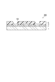
- FIG. 1 to 5 are schematic sectional views showing an embodiment of a manufacturing process of a semiconductor device having a multilayer wiring structure.
- the structure 100 shown in FIG. 1 is prepared.
- the structure 100 includes a semiconductor substrate 1 such as an Si substrate having circuit elements, a protective film 2 such as a silicon oxide film covering the semiconductor substrate 1 having a predetermined pattern from which the circuit elements are exposed, and on the exposed circuit elements.
- the interlayer insulating layer 4 made of a polyimide resin or the like formed on the protective film 2 and the first conductor layer 3 by a spin coating method or the like.
- the photosensitive resin layer 5 is formed, for example, by applying a photosensitive resin such as chlorinated rubber, phenol novolac, polyhydroxystyrene, or polyacrylate ester by a spin coating method.
- the window 6A is formed so that a predetermined portion of the interlayer insulating layer 4 is exposed by a known photolithography technique.
- the photosensitive resin layer 5 is removed to obtain the structure 300 shown in FIG.
- dry etching means using a gas such as oxygen or carbon tetrafluoride can be used.
- the portion of the interlayer insulating layer 4 corresponding to the window portion 6A is selectively removed, and the interlayer insulating layer 4 provided with the window portion 6B so that the first conductor layer 3 is exposed is obtained.
- the photosensitive resin layer 5 is removed using an etching solution that corrodes only the photosensitive resin layer 5 without corroding the first conductor layer 3 exposed from the window 6B.
- the second conductor layer 7 is formed in a portion corresponding to the window portion 6B, and the structure 400 shown in FIG. 4 is obtained.
- a known photolithography technique can be used to form the second conductor layer 7. As a result, the second conductor layer 7 and the first conductor layer 3 are electrically connected.
- the surface protective layer 8 is formed on the interlayer insulating layer 4 and the second conductor layer 7 to obtain the semiconductor device 500 shown in FIG.
- the surface protective layer 8 is formed as follows. First, the photosensitive resin composition of the present embodiment is applied on the interlayer insulating layer 4 and the second conductor layer 7 by spin coating, and dried to form a photosensitive resin film. Next, after light irradiation through a mask on which a pattern corresponding to the window 6C is drawn at a predetermined portion, the photosensitive resin film is patterned by developing with an alkaline aqueous solution. Thereafter, the photosensitive resin film is cured by heating to form a film as the surface protective layer 8.
- the surface protective layer 8 protects the first conductor layer 3 and the second conductor layer 7 from external stress, ⁇ rays, and the like, and the obtained semiconductor device 500 is excellent in reliability.
- the method for manufacturing a semiconductor device having a two-layer wiring structure is shown.
- the above steps are repeated to form each layer.
- the surface protective layer 8 not only the surface protective layer 8 but also the interlayer insulating layer 4 can be formed using the photosensitive resin composition of the present embodiment.
- the electronic component of this embodiment has a pattern cured film formed by the above-described manufacturing method as an interlayer insulating layer or a surface protective layer.
- the pattern cured film can be used as a surface protective layer of a semiconductor device, an interlayer insulating layer, an interlayer insulating layer of a multilayer wiring board, or the like.
- the electronic component of the present embodiment is not particularly limited except that it has a surface protective layer or an interlayer insulating layer formed using the above-described photosensitive resin composition, and can have various structures.
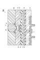
- the above-mentioned photosensitive resin composition is excellent also in stress relaxation property, adhesiveness, etc., it can be used also as various structural materials in the package of various structures developed in recent years. 6 and 7 show a cross-sectional structure of an example of such a semiconductor device.
- FIG. 6 is a schematic cross-sectional view showing a wiring structure as one embodiment of a semiconductor device.
- a semiconductor device 600 shown in FIG. 6 includes a silicon chip 23, an interlayer insulating layer 11 provided on one side of the silicon chip 23, and an Al having a pattern including a pad portion 15 formed on the interlayer insulating layer 11.
- a wiring layer 12, an insulating layer 13 (for example, a P-SiN layer) and a surface protective layer 14 sequentially stacked on the interlayer insulating layer 11 and the Al wiring layer 12 while forming an opening on the pad portion 15, and a surface protective layer; 14 in contact with the pad portion 15 in the openings of the insulating layer 13 and the surface protective layer 14 and the surface of the core 18 opposite to the surface protective layer 14.
- the semiconductor device 600 is formed so as to cover the surface protective layer 14, the core 18, and the rewiring layer 16, and a cover coat layer 19 in which an opening is formed in a portion of the rewiring layer 16 on the core 18.
- the conductive ball 17 connected to the rewiring layer 16 with the barrier metal 20 interposed therebetween in the opening of the layer 19, the collar 21 that holds the conductive ball, and the cover coat layer 19 around the conductive ball 17 are provided.
- the underfill 22 is provided.
- the conductive ball 17 is used as an external connection terminal and is formed of solder, gold or the like.
- the underfill 22 is provided to relieve stress when the semiconductor device 600 is mounted.
- FIG. 7 is a schematic cross-sectional view showing a wiring structure as one embodiment of a semiconductor device.
- an Al wiring layer (not shown) and a pad portion 15 of the Al wiring layer are formed on the silicon chip 23, and an insulating layer 13 is formed on the Al wiring layer.
- a surface protective layer 14 is formed.
- a rewiring layer 16 is formed on the pad portion 15, and the rewiring layer 16 extends to an upper portion of the connection portion 24 with the conductive ball 17. Further, a cover coat layer 19 is formed on the surface protective layer 14. The rewiring layer 16 is connected to the conductive ball 17 through the barrier metal 20.
- the above-described photosensitive resin composition forms not only the interlayer insulating layer 11 or the surface protective layer 14 but also the cover coat layer 19, the core 18, the collar 21, the underfill 22, and the like. Can be used as a material for.
- the cured body using the photosensitive resin composition described above is excellent in adhesion to metal layers (for example, Cu, Au, Ni, Ti, etc.) such as the Al wiring layer 12 and the rewiring layer 16, sealing materials, Since the stress relaxation effect is also high, the semiconductor device in which this cured body is used for the underfill 22 used in the surface protective layer 14, the cover coat layer 19, the core 18, the collar 21, the flip chip, etc. has extremely high reliability. It becomes.
- the photosensitive resin composition of the present embodiment is particularly suitable for use in the surface protective layer 14 and / or the cover coat layer 19 of the semiconductor device having the rewiring layer 16 in FIGS.
- the film thickness of the surface protective layer or the cover coat layer is preferably 3 to 20 ⁇ m, and more preferably 5 to 15 ⁇ m.
- the heating temperature is preferably 100 ° C. to 200 ° C., more preferably 140 ° C. to 200 ° C.
- the pattern cured film formed from the photosensitive resin composition of this embodiment has high mechanical properties. As a result, an electronic component (electronic device) such as a semiconductor device having excellent reliability can be obtained with high yield and high yield.
- A1 and A2 were prepared.
- A2 Prepared by the method described in Synthesis Example 1 below.
- Synthesis Example 1 Synthesis of phenol resin (A2) modified with a compound having an unsaturated hydrocarbon group having 4 to 100 carbon atoms. 100 parts by weight of phenol, 43 parts by weight of tung oil, and 0.1 part by weight of trifluoromethanesulfonic acid were mixed. And stirred at 120 ° C. for 2 hours to obtain a vegetable oil-modified phenol derivative (a). Next, 130 g of the vegetable oil-modified phenol derivative (a), 16.3 g of paraformaldehyde and 1.0 g of oxalic acid were mixed and stirred at 90 ° C. for 3 hours.
- B1 1,2-naphthoquinone-2-diazide-5-sulfonic acid ester of 2,3,4-trihydroxybenzophenone (esterification rate of about 20%, manufactured by Toyo Gosei Co., Ltd., trade name “NT200”)
- C1 1,3-bis (2,3-epoxypropyl) -5- (2-propenyl) -1,3,5-triazine-2,4,6-trione (manufactured by Shikoku Kasei Kogyo Co., Ltd., trade name “ MA-DGIC ”)
- C2 1,3-bis (2,3-epoxypropyl) -5-methyl-1,3,5-triazine-2,4,6-trione (trade name “Me-DGIC” manufactured by Shikoku Kasei Kogyo Co., Ltd.)
- C3 1,3,5-tris (4,5-epoxypentyl) -1,3,5-triazine-2,4,6-trione (trade name “TEPIC-VL” manufactured by Nissan Chemical Industries, Ltd.)
- C4 Polypropylene glycol skeleton-containing bisphenol type epoxy resin (manufactured
- X represents a propylene group having a hydroxy group
- n represents the number of repeating units
- E1 was prepared by the method of Synthesis Example 2 below.
- Synthesis Example 2 Synthesis of acrylic resin E1 To a 500 ml three-necked flask equipped with a stirrer, a nitrogen introduction tube and a thermometer, 75 g of toluene and 75 g of isopropanol (IPA) were weighed and separately weighed butyl acrylate (BA). 85 g, 24 g lauryl acrylate (LA), 14 g acrylic acid (AA), and 0.13 g azobisisobutyronitrile (AIBN) were added.
- LA lauryl acrylate
- AA acrylic acid
- AIBN 0.13 g azobisisobutyronitrile
- Example 1 ⁇ Formulation of photosensitive resin composition> (Example 1) A1 (70 g), B1 (10 g), C1 (15 g) and H1 (110 g) were weighed and added to a plastic container and stirred at room temperature (25 ° C.) until evenly dissolved. Thereafter, A2 (10 g) and E1 (20 g) were further added, and the mixture was stirred at room temperature until evenly dissolved. This solution was subjected to pressure filtration using a 3 ⁇ m pore Teflon (registered trademark) filter to prepare a photosensitive resin composition of Example 1. The blending amounts (unit: grams) of the components (A), (B), (C), (E) and (H) are shown in Table 1.
- ⁇ Resolution evaluation of photosensitive resin composition The photosensitive resin compositions obtained in Examples 1 to 9 and Comparative Examples 1 to 6 were spin coated on a silicon substrate and heated at 110 ° C. for 2 minutes to form a resin film having a thickness of about 11 to 12 ⁇ m. .
- the resin film was exposed at all wavelengths through a mask using a proximity exposure machine (trade name “PLA-600FA” manufactured by Canon Inc.). After the exposure, development was performed using a 2.38 mass% aqueous solution of TMAH (tetramethylammonium hydroxide) to obtain a rectangular pattern having a width of 10 mm. Whether the film was developed or not was evaluated as the resolution as follows.
- TMAH tetramethylammonium hydroxide
- hydrofluoric acid peeling is possible, it can be said that the pattern cured film using the photosensitive resin composition is excellent in mechanical characteristics.
- A hydrofluoric acid peelable
- B Hydrofluoric acid cannot be removed
- ND The film was brittle and a measurement sample could not be prepared.
- the average of the measured values of five or more test pieces obtained from the cured film obtained under the same conditions was defined as elongation at break and elastic modulus (tensile elastic modulus), and the results are shown in Table 1.
- the elongation at break is preferably 5% or more, and it can be said that the mechanical properties are particularly excellent when it is 12% or more.
- “ND” The film was brittle and a measurement sample could not be prepared.
- the photosensitive resin compositions of Examples 1 to 9 were able to provide cured films having sufficient toughness even at low temperature curing and showing good mechanical properties. Particularly in Examples 7 and 8 using the component (C) having two different skeletons, the patterned cured film is more excellent in elongation at break and excellent in mechanical strength. On the other hand, in Comparative Examples 1 and 6 in which no epoxy crosslinking agent was used, the obtained cured film was very brittle, and the film collapsed during the hydrofluoric acid peeling. Therefore, data such as elongation at break were not obtained. Further, in Comparative Example 2 using an epoxy crosslinking agent having a cycloalkyl group, which is different from the epoxy crosslinking agent in the present invention, the resolution was lowered.
- SYMBOLS 1 ... Semiconductor substrate, 2 ... Protective film, 3 ... 1st conductor layer, 4 ... Interlayer insulation layer, 5 ... Photosensitive resin layer, 6A, 6B, 6C ... Window part, 7 ... 2nd conductor layer, 8 ... Surface protection 11 ... Interlayer insulating layer 12 ... Wiring layer 13 ... Insulating layer 14 ... Surface protective layer 15 ... Pad portion 16 ... Rewiring layer 17 ... Conductive ball 18 ... Core 19 ... Cover coat layer 20 ... Barrier metal, 21 ... Color, 22 ... Underfill, 23 ... Silicon chip, 24 ... Connection part, 100, 200, 300, 400 ... Structure, 500 ... Semiconductor device, 600 ... Semiconductor device, 700 ... Semiconductor device .
Abstract
本発明は、(A)ポリヒドロキシスチレン樹脂及び/又はフェノール樹脂と、(B)光により酸を生成する化合物と、(C)所定の構造を有するエポキシ架橋剤と、を含有する感光性樹脂組成物を提供する。
Description
本発明は、感光性樹脂組成物、並びにそれを用いたパターン硬化膜の製造方法及び電子部品に関する。
半導体素子の高集積化、小型化及び微細化に伴い、半導体素子の表面保護層、層間絶縁層及び再配線層を形成するために用いられる感光性樹脂組成物には、より優れた感度、解像度を併せ持ち、より微細で精密なパターン硬化膜を形成可能であることが求められている。さらに、これらの感光性樹脂組成物から形成されるパターン硬化膜には、デバイスの信頼性を高める観点から、高い機械特性(破断伸び及び弾性率)を併せ持つことが望まれている。このような特性を併せ持つ材料として、例えば特許文献1にはポリイミド樹脂を含有する感光性樹脂組成物が開示されており、特許文献2にはエポキシ基を有するポリイミド樹脂を含有する感光性樹脂組成物が提案されている。
特許文献1等のポリイミド樹脂を含有する感光性樹脂組成物は、高い解像性を有し、且つこの感光性樹脂組成物から形成されるパターン硬化膜は、耐熱性、絶縁性、透明性等に優れるという利点がある。しかしながら、ポリイミド樹脂は硬化温度が非常に高いため、高い機械特性を実現するために感光性樹脂組成物を高温で硬化させなければならず、熱収縮等によるデバイスへのダメージが大きくなってしまうという問題がある。
一方、特許文献2等のエポキシ基を有するポリイミド樹脂を含有する感光性樹脂組成物は、比較的低温で硬化することが可能であるものの、機械特性が低下してしまう問題があり、低温での硬化と機械特性の2つの特性を両立させることは困難である。
そこで本発明は、低温で硬化することができ、且つ良好な解像性を有するとともに、高い機械特性を有するパターン硬化膜を形成することが可能な感光性樹脂組成物を提供することを目的とする。また本発明は、この感光性樹脂組成物を用いたパターン硬化膜の製造方法、該製造方法により形成されたパターン硬化膜を有する電子部品を提供することを目的とする。
本発明は以下のものに関する。
<1> (A)ポリヒドロキシスチレン樹脂及び/又はフェノール樹脂と、(B)光により酸を生成する化合物と、(C)下記一般式(1)、(2)又は(3)で表されるエポキシ架橋剤と、を含有する感光性樹脂組成物。

[一般式(1)、(2)及び(3)中、R1は、アルキル基、アルケニル基又はアルキニル基を示し、R2は、それぞれ独立に水素原子又はメチル基を示し、R3は、1つ以上のヒドロキシ基を有するアルキレン基を示し、nは、1~5の整数を示し、mは、2~5の整数を示し、lは、0~6の整数を示す。]
<2> (C)成分の含有量が、(A)成分100質量部に対して5~75質量部である、請求項1に記載の感光性樹脂組成物。
<3> (C)成分として、一般式(1)、(2)又は(3)で表されるいずれかのエポキシ架橋剤のうち2種以上を含む、<1>又は<2>に記載の感光性樹脂組成物。
<4> (A)成分が、フェノール樹脂である<1>~<3>のいずれかに記載の感光性樹脂組成物。
<5> (A)成分が、不飽和炭化水素基を有しないフェノール樹脂(A1)、及び不飽和炭化水素基を有する変性フェノール樹脂(A2)を含む、<1>~<3>のいずれかに記載の感光性樹脂組成物。
<6> (A2)成分が、フェノール性水酸基と多塩基酸無水物との反応によってさらに変性された変性フェノール樹脂である、<5>に記載の感光性樹脂組成物。
<7> (B)成分が、o-キノンジアジド化合物である、<1>~<6>のいずれかに記載の感光性樹脂組成物。
<8> (E)アクリル樹脂をさらに含有する、<1>~<7>のいずれかに記載の感光性樹脂組成物。
<9> <1>~<8>のいずれかに記載の感光性樹脂組成物を基板上に塗布及び乾燥して感光性樹脂膜を形成する工程と、感光性樹脂膜を露光する工程と、露光後の感光性樹脂膜をアルカリ水溶液によって現像して、パターン樹脂膜を形成する工程と、パターン樹脂膜を加熱する工程と、を備えるパターン硬化膜の製造方法。
<10> <9>に記載の製造方法により得られるパターン硬化膜を表面保護層又は層間絶縁層として有する電子部品。
<11> <9>に記載の製造方法により得られるパターン硬化膜をカバーコート層、コア、カラー又はアンダーフィルとして有する電子部品。
<1> (A)ポリヒドロキシスチレン樹脂及び/又はフェノール樹脂と、(B)光により酸を生成する化合物と、(C)下記一般式(1)、(2)又は(3)で表されるエポキシ架橋剤と、を含有する感光性樹脂組成物。
[一般式(1)、(2)及び(3)中、R1は、アルキル基、アルケニル基又はアルキニル基を示し、R2は、それぞれ独立に水素原子又はメチル基を示し、R3は、1つ以上のヒドロキシ基を有するアルキレン基を示し、nは、1~5の整数を示し、mは、2~5の整数を示し、lは、0~6の整数を示す。]
<2> (C)成分の含有量が、(A)成分100質量部に対して5~75質量部である、請求項1に記載の感光性樹脂組成物。
<3> (C)成分として、一般式(1)、(2)又は(3)で表されるいずれかのエポキシ架橋剤のうち2種以上を含む、<1>又は<2>に記載の感光性樹脂組成物。
<4> (A)成分が、フェノール樹脂である<1>~<3>のいずれかに記載の感光性樹脂組成物。
<5> (A)成分が、不飽和炭化水素基を有しないフェノール樹脂(A1)、及び不飽和炭化水素基を有する変性フェノール樹脂(A2)を含む、<1>~<3>のいずれかに記載の感光性樹脂組成物。
<6> (A2)成分が、フェノール性水酸基と多塩基酸無水物との反応によってさらに変性された変性フェノール樹脂である、<5>に記載の感光性樹脂組成物。
<7> (B)成分が、o-キノンジアジド化合物である、<1>~<6>のいずれかに記載の感光性樹脂組成物。
<8> (E)アクリル樹脂をさらに含有する、<1>~<7>のいずれかに記載の感光性樹脂組成物。
<9> <1>~<8>のいずれかに記載の感光性樹脂組成物を基板上に塗布及び乾燥して感光性樹脂膜を形成する工程と、感光性樹脂膜を露光する工程と、露光後の感光性樹脂膜をアルカリ水溶液によって現像して、パターン樹脂膜を形成する工程と、パターン樹脂膜を加熱する工程と、を備えるパターン硬化膜の製造方法。
<10> <9>に記載の製造方法により得られるパターン硬化膜を表面保護層又は層間絶縁層として有する電子部品。
<11> <9>に記載の製造方法により得られるパターン硬化膜をカバーコート層、コア、カラー又はアンダーフィルとして有する電子部品。
本発明によれば、低温(例えば200℃以下)で硬化することができ、且つ良好な感光特性(感度及び解像度)を有する感光性樹脂組成物を提供することができる。また、この感光性樹脂組成物から形成されるパターン硬化膜は、十分な機械特性(フッ酸剥離性、破断伸び及び弾性率)を有する。本発明の感光性樹脂組成物は、低温での硬化が可能であるため、電子部品への熱によるダメージを防止することができ、信頼性の高い電子部品を歩留まり良く提供することができる。
本発明の一実施形態について詳細に説明するが、本発明は以下の実施形態に限定されるものではない。また本明細書において「~」は、その前後に記載される数値をそれぞれ最小値および最大値として含む範囲を示すものとする。また本明細書において、「(メタ)アクリレート」とは、「アクリレート」及びそれに対応する「メタクリレート」を意味する。「(メタ)アクリル酸」等の他の類似の表現においても同様である。
[感光性樹脂組成物]
本実施形態の感光性樹脂組成物は、(A)ポリヒドロキシスチレン樹脂及び/又はフェノール樹脂と、(B)光により酸を生成する化合物と、(C)所定の構造を有するエポキシ架橋剤と、を含有する。
本実施形態の感光性樹脂組成物は、(A)ポリヒドロキシスチレン樹脂及び/又はフェノール樹脂と、(B)光により酸を生成する化合物と、(C)所定の構造を有するエポキシ架橋剤と、を含有する。
<(A)成分:ポリヒドロキシスチレン樹脂及び/又はフェノール樹脂>
ポリヒドロキシスチレン樹脂としては、ポリヒドロキシスチレン及びヒドロキシスチレンを単量体単位として含む共重合体等を用いることができる。また、フェノール樹脂としては、フェノール又はその誘導体とアルデヒド類との重縮合生成物を用いることができる。
ポリヒドロキシスチレン樹脂としては、ポリヒドロキシスチレン及びヒドロキシスチレンを単量体単位として含む共重合体等を用いることができる。また、フェノール樹脂としては、フェノール又はその誘導体とアルデヒド類との重縮合生成物を用いることができる。
(A)成分としては、低価格であること及び硬化時の体積収縮が小さいことから、フェノール樹脂が好ましく、ノボラック型フェノール樹脂がより好ましい。なお、ノボラック型フェノール樹脂としては、例えば特開2008-309885号公報に記載のものが好ましい。
(A)成分の重量平均分子量(Mw)は、アルカリ水溶液に対する溶解性、感光特性及び機械物性とのバランスを考慮すると、500~150000であることが好ましく、500~100000であることがより好ましく、1000~50000であることがさらに好ましい。ここで、重量平均分子量は、ゲルパーミエーションクロマトグラフィー法により測定し、標準ポリスチレン検量線より換算して得られる値である。
(A)成分は、不飽和炭化水素基を有しないフェノール樹脂(A1)と不飽和炭化水素基を有する変性フェノール樹脂(A2)を含んでいてもよい。さらに、(A2)成分はフェノール性水酸基と多塩基酸無水物との反応によってさらに変性されているものでもよい。(A2)成分を含有させることで硬化膜の密着性及び耐熱衝撃性が向上する。
(A2)成分は、一般に、フェノール又はその誘導体と不飽和炭化水素基を有する化合物(好ましくは炭素数が4~100の、不飽和炭化水素基を有する化合物)(以下場合により単に「不飽和炭化水素基含有化合物」という。)との反応生成物(以下「不飽和炭化水素基変性フェノール誘導体」という。)と、アルデヒド類との縮重合生成物、又は、フェノール樹脂と不飽和炭化水素基含有化合物との反応生成物である。(A2)成分を得るために用いられるフェノール誘導体としては、フェノール樹脂を得るために用いられるフェノール誘導体及びアルデヒド類と同様のものを用いることができる。(A2)成分としては、例えば国際公開第2009/063808号又は国際公開第2010/026988号に記載のものが好ましい。
(A2)成分の酸価は、30~200mgKOH/gであることが好ましく、40~170mgKOH/gであることがより好ましく、50~150mgKOH/gであることがさらに好ましい。酸価が30mgKOH/g以上であると、アルカリ現像が短時間で済む傾向にあり、200mgKOH/g以下であると、未露光部の耐現像液性が向上する傾向にある。
(A2)成分の分子量は、アルカリ水溶液に対する溶解性及び感光特性とパターン硬化膜の機械特性とのバランスを考慮すると、重量平均分子量で1000~500000が好ましく、2000~200000がより好ましく、2000~100000であることがさらに好ましい。ここで、重量平均分子量は、ゲルパーミエーションクロマトグラフィー法により測定し、標準ポリスチレン検量線より換算して得た値である。
感光性樹脂組成物は、パターン樹脂膜を形成する際の感度と解像性、並びに硬化後のパターン硬化膜の密着性、機械特性及び耐熱衝撃性の点から、(A)成分として、不飽和炭化水素基を有する変性フェノール樹脂(A2)を混合して用いる場合、(A)成分中に、不飽和炭化水素基を有しないフェノール樹脂(A1)と、不飽和炭化水素基を有する変性フェノール樹脂(A2)の質量比が両者の合計量を100として前者(A1):後者(A2)で5:95~95:5で含まれることが好ましく、8:92~92:8含まれることがより好ましい。
<(B)成分:光により酸を生成する化合物>
(B)成分である光により酸を生成する化合物は、感光剤として用いられる。(B)成分は、光照射により酸を生成させ、光照射した部分のアルカリ水溶液への可溶性を増大させる機能を有する。(B)成分としては、一般に光酸発生剤と称される化合物を用いることができる。(B)成分の具体例としては、o-キノンジアジド化合物、アリールジアゾニウム塩、ジアリールヨードニウム塩、トリアリールスルホニウム塩等が挙げられる。これらの中で、感度が高いことから、o-キノンジアジド化合物が好ましい。
(B)成分である光により酸を生成する化合物は、感光剤として用いられる。(B)成分は、光照射により酸を生成させ、光照射した部分のアルカリ水溶液への可溶性を増大させる機能を有する。(B)成分としては、一般に光酸発生剤と称される化合物を用いることができる。(B)成分の具体例としては、o-キノンジアジド化合物、アリールジアゾニウム塩、ジアリールヨードニウム塩、トリアリールスルホニウム塩等が挙げられる。これらの中で、感度が高いことから、o-キノンジアジド化合物が好ましい。
o-キノンジアジド化合物は、例えば、o-キノンジアジドスルホニルクロリドと、ヒドロキシ化合物、アミノ化合物等とを脱塩酸剤の存在下で縮合反応させる方法により得られる。
反応に用いられるo-キノンジアジドスルホニルクロリドとしては、例えば、1,2-ベンゾキノン-2-ジアジド-4-スルホニルクロリド、1,2-ナフトキノン-2-ジアジド-5-スルホニルクロリド、1,2-ナフトキノン-2-ジアジド-4-スルホニルクロリド等が挙げられる。
反応に用いられるヒドロキシ化合物としては、例えば、ヒドロキノン、レゾルシノール、ピロガロール、ビスフェノールA、ビス(4-ヒドロキシフェニル)メタン、2,2-ビス(4-ヒドロキシフェニル)ヘキサフルオロプロパン、2,3,4-トリヒドロキシベンゾフェノン、2,3,4,4’-テトラヒドロキシベンゾフェノン、2,2’,4,4’-テトラヒドロキシベンゾフェノン、2,3,4,2’,3’-ペンタヒドロキシベンゾフェノン、2,3,4,3’,4’,5’-ヘキサヒドロキシベンゾフェノン、ビス(2,3,4-トリヒドロキシフェニル)メタン、ビス(2,3,4-トリヒドロキシフェニル)プロパン、4b,5,9b,10-テトラヒドロ-1,3,6,8-テトラヒドロキシ-5,10-ジメチルインデノ[2,1-a]インデン、トリス(4-ヒドロキシフェニル)メタン、トリス(4-ヒドロキシフェニル)エタン、1,1-ビス(4-ヒドロキシフェニル)-1-[4-{1-(4-ヒドロキシフェニル)-1-メチルエチル}フェニル]エタン等が挙げられる。
反応に用いられるアミノ化合物としては、例えば、p-フェニレンジアミン、m-フェニレンジアミン、4,4’-ジアミノジフェニルエーテル、4,4’-ジアミノジフェニルメタン、4,4’-ジアミノジフェニルスルホン、4,4’-ジアミノジフェニルスルフィド、o-アミノフェノール、m-アミノフェノール、p-アミノフェノール、3,3’-ジアミノ-4,4’-ジヒドロキシビフェニル、4,4’-ジアミノ-3,3’-ジヒドロキシビフェニル、ビス(3-アミノ-4-ヒドロキシフェニル)プロパン、ビス(4-アミノ-3-ヒドロキシフェニル)プロパン、ビス(3-アミノ-4-ヒドロキシフェニル)スルホン、ビス(4-アミノ-3-ヒドロキシフェニル)スルホン、ビス(3-アミノ-4-ヒドロキシフェニル)ヘキサフルオロプロパン、ビス(4-アミノ-3-ヒドロキシフェニル)ヘキサフルオロプロパン等が挙げられる。
これらの中でも吸収波長範囲と反応性の点から、1,1-ビス(4-ヒドロキシフェニル)-1-[4-{1-(4-ヒドロキシフェニル)-1-メチルエチル}フェニル]エタンと1,2-ナフトキノン-2-ジアジド-5-スルホニルクロリドとを縮合反応して得られたもの又はトリス(4-ヒドロキシフェニル)メタン若しくはトリス(4-ヒドロキシフェニル)エタンと1,2-ナフトキノン-2-ジアジド-5-スルホニルクロリドとを縮合反応して得られたものを用いることが好ましい。
反応に用いられる脱塩酸剤としては、例えば、炭酸ナトリウム、水酸化ナトリウム、炭酸水素ナトリウム、炭酸カリウム、水酸化カリウム、トリメチルアミン、トリエチルアミン、ピリジン等が挙げられる。また、反応溶媒としては、例えば、ジオキサン、アセトン、メチルエチルケトン、テトラヒドロフラン、ジエチルエーテル、N-メチルピロリドン等が用いられる。
o-キノンジアジドスルホニルクロリドと、ヒドロキシ化合物及び/又はアミノ化合物とは、o-キノンジアジドスルホニルクロリド1モルに対して、ヒドロキシ基とアミノ基とのモル数の合計が0.5~1になるように配合されることが好ましい。脱塩酸剤とo-キノンジアジドスルホニルクロリドの好ましい配合割合は、0.95/1モル当量~1/0.95モル当量の範囲である。
上述の反応の好ましい反応温度は0~40℃、好ましい反応時間は1~10時間である。
(B)成分の含有量は、露光部と未露光部の溶解速度差が大きくなり、感度がより良好となる点から、(A)成分100質量部に対して3~100質量部が好ましく、5~50質量部がより好ましく、5~30質量部がさらに好ましい。
<(C)成分:エポキシ架橋剤>
(C)成分であるエポキシ架橋剤は、下記一般式(1)、(2)又は(3)で表される構造を有し、パターン樹脂膜を加熱処理する際に、(A)成分と反応して架橋構造を形成し得る化合物である。これらを用いることにより、膜に機械特性を与え、また、パターン硬化膜のメルトを抑制することができる。
(C)成分であるエポキシ架橋剤は、下記一般式(1)、(2)又は(3)で表される構造を有し、パターン樹脂膜を加熱処理する際に、(A)成分と反応して架橋構造を形成し得る化合物である。これらを用いることにより、膜に機械特性を与え、また、パターン硬化膜のメルトを抑制することができる。

[一般式(1)、(2)及び(3)中、R1はアルキル基、アルケニル基又はアルキニル基を示し、R2は、それぞれ独立に水素原子又はメチル基を示し、R3は、1つ以上のヒドロキシ基を有するアルキレン基を示す。nは、1~5の整数、mは、2~5の整数、lは0~6の整数を示す。]
R1において、アルキル基としては、一般式CnH2n+1-(nは1~20の整数)で表される、メチル基、エチル基、プロピル基、ブチル基、イソプロピル基、tert-ブチル基等が例示され、アルケニル基としては、一般式CnH2n-1-(nは1~20の整数)で表される、ビニル基、アリル基、ブテニル基等が例示され、アルキニル基としては、一般式CnH2n-3-(nは1~20の整数)で表される、エチニル基、プロパギル基等が例示される。
これらの中で、R1は炭素数1~10のアルキル基又は炭素数1~10のアルケニル基であることが好ましく、炭素数1~6のアルキル基又は炭素数1~6のアルケニル基であることがより好ましい。
R3において、1つ以上のヒドロキシ基を有するアルキレン基としては、一般式-(CH2)n-(nは3~10の整数)で表される、プロピレン基、トリメチレン基、テトラメチレン基等における水素原子の一つ以上がヒドロキシ基で置換された基などが例示される。ヒドロキシ基の数は、1又は2であることが好ましい。1つ以上のヒドロキシ基を有するアルキレン基は、例えば、フェノール性水酸基とグリシジル基との反応により形成することができる。
一般にエポキシ化合物、現像液(アルカリ水溶液)に溶けにくいため、化合物の極性を上げる必要がある。しかし極性を上げると、未露光部まで溶解し、コントラスト(露光部と未露光部の溶解速度の違い)が低下してしまう問題がある。これに対して、一般式(1)、(2)又は(3)で表されるエポキシ架橋剤を用いることにより、アルカリ現像性とコントラストを両立することが可能である。
これらエポキシ架橋剤成分の構造を変えることで、感光性樹脂組成物のアルカリ解像性を調整することができる。例えば一般式(1)又は(2)で表される、極性の高いイソシアヌレート環を有するエポキシ架橋剤を用いることで露光部のアルカリ溶解性を強めることができ、逆に一般式(3)で表される、極性の低いベンゼン環を有するエポキシ架橋剤を用いることで未露光部の溶解を抑えることができる。
このような(C)成分は、例えば100℃~250℃程度の温度で(A)成分と架橋することができる。なお、(A)成分と(C)成分の架橋温度は、DSC測定(示差走査熱量測定)で観察される発熱ピーク温度によって評価する。DSCの測定条件は以下の通りである。
測定装置:ティー・エイ・インスツルメント・ジャパン株式会社製Q200
サンプル量:5mg
昇温速度:5℃/min
測定雰囲気:窒素
サンプル量:5mg
昇温速度:5℃/min
測定雰囲気:窒素
一般式(1)で示されるエポキシ架橋剤としては、例えば、1,3-ビス(2,3-エポキシプロピル)-5-メチル-1,3,5-トリアジン-2,4,6-トリオン、1,3-ビス(2,3-エポキシプロピル)-5-(2-プロペニル)-1,3,5-トリアジン-2,4,6-トリオン、1,3-ビス(2,3-エポキシプロピル)-5-エチル-1,3,5-トリアジン-2,4,6-トリオン、1,3-ビス(2,3-エポキシプロピル)-5-プロピル-1,3,5-トリアジン-2,4,6-トリオン、1-ブチル-3,5-ビス(2,3-エポキシプロピル)-1,3,5-トリアジン-2,4,6-トリオン、1,3-ビス(2,3-エポキシプロピル)-5-ペンチル-1,3,5-トリアジン-2,4,6-トリオン、1,3-ビス(2,3-エポキシプロピル)-5-へキシル-1,3,5-トリアジン-2,4,6-トリオン、1,3-ビス(2,3-エポキシプロピル)-5-ペンチル-1,3,5-トリアジン-2,4,6-トリオン、1,3-ビス(2,3-エポキシプロピル)-5-(1-メチルエチル)-1,3,5-トリアジン-2,4,6-トリオン、1,3-ビス(2,3-エポキシプロピル)-5-エチニル-1,3,5-トリアジン-2,4,6-トリオン等が挙げられる。
一般式(2)で示されるエポキシ架橋剤としては、例えば、1,3,5-トリス(3,4-エポキシブチル)-1,3,5-トリアジン-2,4,6-トリオン、1,3,5-トリス(4,5-エポキシペンチル)-1,3,5-トリアジン-2,4,6-トリオン、1,3,5-トリス(5,6-エポキシヘキシル)-1,3,5-トリアジン-2,4,6-トリオン、1,3,5-トリス(6,7-エポキシヘプチル)-1,3,5-トリアジン-2,4,6-トリオン等が挙げられる。
一般式(3)で表される化合物としては、例えば、ビス[4-(グリシドキシ)フェニル]メタン、2,2-ビス[4-(グリシドキシ)フェニル]プロパン、1,4-ビス[4-{ジメチル(4-[グリシドキシ]フェニル)メチル}フェノキシ]-2,3-ブタンジオール、1,4-ビス[4-{(4-[グリシドキシ]フェニル)メチル}フェノキシ]-2,3-ブタンジール等が挙げられる。
これらの化合物の中でも、機械物性の観点から、1,3-ビス(2,3-エポキシプロピル)-5-(2-プロペニル)-1,3,5-トリアジン-2,4,6-トリオン、1,3-ビス(2,3-エポキシプロピル)-5-メチル-1,3,5-トリアジン-2,4,6-トリオン、1,3,5-トリス(4,5-エポキシペンチル)-1,3,5-トリアジン-2,4,6-トリオン、2,2-ビス[4-(グリシドキシ)フェニル]プロパン又は1,4-ビス[4-{ジメチル(4-[グリシドキシ]フェニル)メチル}フェノキシ]-2,3-ブタンジオールを用いることが好ましく、現像性の観点から1,3-ビス(2,3-エポキシプロピル)-5-(2-プロペニル)-1,3,5-トリアジン-2,4,6-トリオン、1,3-ビス(2,3-エポキシプロピル)-5-メチル-1,3,5-トリアジン-2,4,6-トリオン又は1,3,5-トリス(4,5-エポキシペンチル)-1,3,5-トリアジン-2,4,6-トリオンを用いることがより好ましく、1,3-ビス(2,3-エポキシプロピル)-5-(2-プロペニル)-1,3,5-トリアジン-2,4,6-トリオンを用いることがさらに好ましい。
また、(C)成分の含有量は、(A)成分100質量部に対して、5~75質量部であることが好ましく、5~40質量部であることがより好ましく、10~30質量%であることがさらに好ましい。(C)成分が、5質量%以上であると、膜の機械特性がより向上する傾向にあり、75質量%以下であると、アルカリ解像性がより向上する傾向がある。
(C)成分としては、硬化膜の機械物性は良好であるがアルカリ解像性が比較的低い一般式(3)で表されるエポキシ架橋剤と、アルカリ解像性の良好な一般式(1)又は(2)で表されるエポキシ架橋剤とを併用することが好ましい。これによる相乗効果により両方の特性が良好な硬化膜を得ることができる。
一般式(3)で表されるエポキシ架橋剤としての2,2-ビス[4-(グリシドキシ)フェニル]プロパン又は1,4-ビス[4-{ジメチル(4-[グリシドキシ]フェニル)メチル}フェノキシ]-2,3-ブタンジオールと、一般式(1)又は(2)で表されるエポキシ架橋剤としての1,3-ビス(2,3-エポキシプロピル)-5-(2-プロペニル)-1,3,5-トリアジン-2,4,6-トリオン、1,3-ビス(2,3-エポキシプロピル)-5-メチル-1,3,5-トリアジン-2,4,6-トリオン又は1,3,5-トリス(4,5-エポキシペンチル)-1,3,5-トリアジン-2,4,6-トリオンとを併用することがより好ましく、2,2-ビス[4-(グリシドキシ)フェニル]プロパン又は1,4-ビス[4-{ジメチル(4-[グリシドキシ]フェニル)メチル}フェノキシ]-2,3-ブタンジオールと、1,3-ビス(2,3-エポキシプロピル)-5-(2-プロペニル)-1,3,5-トリアジン-2,4,6-トリオンとを併用することがさらに好ましい。
また、一般式(3)で表されるエポキシ架橋剤と一般式(1)又は(2)で表されるエポキシ架橋剤とを併用する場合、その質量比が両者の合計量を100として[一般式(3)で表されるエポキシ架橋剤]:[一般式(1)又は(2)で表されるエポキシ架橋剤]で、5:95~95:5で含まれることが好ましく、40:60~90:10含まれることがより好ましい。
これらのエポキシ架橋剤は、必要であれば架橋触媒と共に用いてもよい。架橋触媒としては、アミン類、イミダゾール類、メルカプタン類、酸無水物類、リン酸塩類、熱酸発生剤等が挙げられる。これらの1種を単独で又は2種以上を組み合わせて用いてもよい。
<(D)成分:シラン化合物>
本実施形態の感光性樹脂組成物は、基板との密着性を向上させる観点から、(D)成分として、一般式(4)で表されるエポキシ基を有するシラン化合物を含有していてもよい。
本実施形態の感光性樹脂組成物は、基板との密着性を向上させる観点から、(D)成分として、一般式(4)で表されるエポキシ基を有するシラン化合物を含有していてもよい。
[一般式(4)中、R4は、2価の有機基を表し、R5は1価の有機基を表す。]
一般式(4)において、R4は2価の有機基であるものであれば特に制限はない。感度及び解像度の向上という観点から、R4は-(CH2)n-(nは1~6の整数)で示される直鎖のアルキレン基であることが好ましい。また、一般式(4)において、R5は有機基であるものであれば特に制限はない。感度及び解像度の向上という観点から、R5はアルコキシ基又はアルコキシアルキル基を含むことが好ましい。その中でも特に、安価で手に入りやすいことや、基板への接着性の向上という観点から、メトキシ基又はエトキシ基のようなアルコキシ基を含むことが特に好ましい。このような化合物としては、3-グリシドキシプロピルトリメトキシシラン、3-グリシドキシプロピルトリエトキシシラン等が挙げられる。また、本実施形態の感光性樹脂組成物は(D)一般式(4)で示されるエポキシ基を有するシラン化合物の他に、(D)成分以外のシラン化合物をさらに含んでいてもよい。
(D)成分を用いる場合の含有量は、配線への接着性と感光性樹脂組成物の保存安定性の観点から、(A)成分100質量部に対して、(D)成分と(D)成分以外のシラン化合物の総量が0.1~20質量部であることが好ましく、0.5~10質量部がより好ましく、1~5質量部がさらに好ましい。
<(E)成分:アクリル樹脂>
本実施形態の感光性樹脂組成物は、(E)成分としてアクリル樹脂を含有することが好ましい。アクリル樹脂としては、下記一般式(6)又は(7)で表される構造単位を有するアクリル樹脂であることが好ましい。感光性樹脂組成物が、一般式(6)又は(7)で表される構造単位を有するアクリル樹脂を含有することにより、良好な感光特性を維持しつつ、耐熱衝撃性を向上することができる。(E)成分は、上記アクリル樹脂の1種のみからなるものであってもよく、2種以上を含むものであってもよい。
本実施形態の感光性樹脂組成物は、(E)成分としてアクリル樹脂を含有することが好ましい。アクリル樹脂としては、下記一般式(6)又は(7)で表される構造単位を有するアクリル樹脂であることが好ましい。感光性樹脂組成物が、一般式(6)又は(7)で表される構造単位を有するアクリル樹脂を含有することにより、良好な感光特性を維持しつつ、耐熱衝撃性を向上することができる。(E)成分は、上記アクリル樹脂の1種のみからなるものであってもよく、2種以上を含むものであってもよい。

[一般式(6)及び(7)中、R6は、炭素数4~20のアルキル基を表し、R7は、水素原子又はメチル基を表す。]
また、上記一般式(6)中、感度、解像度及び耐熱衝撃を向上できる観点から、R6が炭素数4~16のアルキル基が好ましく、炭素数4のアルキル基、中でもn-ブチル基がより好ましい。
一般式(6)で表される構造単位を与える重合性単量体としては、対応する(メタ)アクリル酸アルキルエステルが挙げられる。
また、一般式(7)で表される構造単位を与える重合性単量体としては、アクリル酸及びメタクリル酸が挙げられる。
また、一般式(7)で表される構造単位を与える重合性単量体としては、アクリル酸及びメタクリル酸が挙げられる。
(E)成分において、上記一般式(6)で表される構造単位の組成比は、(E)成分の総量に対して、50~95モル%であることが好ましく、60~90モル%であることがより好ましく、70~85モル%であることが特に好ましい。上記一般式(6)で表される構造単位の組成比が50~95モル%であることにより、感光性樹脂組成物の硬化膜の耐熱衝撃性をより向上することができる。
また、(E)成分であるアクリル樹脂において、上記一般式(7)で表される構造単位の組成比は、(E)成分の総量に対して、5~50モル%であることが好ましく、10~40モル%であることがより好ましく、15~30モル%であることがさらに好ましい。
上記一般式(7)で表される構造単位の組成比が5~50モル%であることにより、(A)成分との相溶性、及び感光性樹脂組成物の現像性をより向上することができる。
上記一般式(7)で表される構造単位の組成比が5~50モル%であることにより、(A)成分との相溶性、及び感光性樹脂組成物の現像性をより向上することができる。
(E)成分の重量平均分子量は、2000~100000であることが好ましく、3000~60000であることがより好ましく、4000~50000であることがさらに好ましい。重量平均分子量が2000未満では硬化膜の耐熱衝撃性が低下する傾向があり、100000を超えると(A)成分との相溶性及び現像性が低下する傾向がある。
(E)成分を含有する場合の含有量は、密着性、機械特性、耐熱衝撃性、及び感光特性の観点から、(A)成分の総量100質量部に対して1~50質量部が好ましく、3~30質量部がより好ましく、5~20質量部が特に好ましい。
<(H):溶剤>
本実施形態の感光性樹脂組成物は、基板上への塗布性、及び均一な厚さの樹脂膜を形成できるという観点から、(H)溶剤を含有していてもよい。溶剤の具体例としては、γ-ブチロラクトン、乳酸エチル、プロピレングリコールモノメチルエーテルアセテート、酢酸ベンジル、n-ブチルアセテート、エトキシエチルプロピオナート、3-メチルメトキシプロピオナート、N-メチル-2-ピロリドン、N,N-ジメチルホルムアミド、N,N-ジメチルアセトアミド、ジメチルスルホキシド、ヘキサメチルホスホリルアミド、テトラメチレンスルホン、ジエチルケトン、ジイソブチルケトン、メチルアミルケトン、シクロヘキサノン、プロピレングリコールモノメチルエーテル、プロピレングリコールモノプロピルエーテル、プロピレングリコールモノブチルエーテル及びジプロピレングリコールモノメチルエーテルが挙げられる。これらの溶剤は1種を単独で又は2種以上を組み合わせて用いることができる。
(H)成分を含有させる場合の含有量は、特に限定されないが、感光性樹脂組成物中の溶剤の割合が20~90質量%となるように調整されることが好ましい。
<その他の成分>
本実施形態の感光性樹脂組成物は必要に応じ、熱酸発生剤、エラストマー、溶剤、溶解促進剤、溶解阻害剤、界面活性剤、レベリング剤等のその他の成分を含有することができる。
本実施形態の感光性樹脂組成物は必要に応じ、熱酸発生剤、エラストマー、溶剤、溶解促進剤、溶解阻害剤、界面活性剤、レベリング剤等のその他の成分を含有することができる。
本実施形態の感光性樹脂組成物は、水酸化ナトリウム、水酸化カリウム、ケイ酸ナトリウム、アンモニア、エチルアミン、ジエチルアミン、トリエチルアミン、トリエタノールアミン、水酸化テトラメチルアンモニウム(TMAH)等のアルカリ水溶液を用いて現像することが可能である。また、本実施形態の感光性樹脂組成物は良好な感光特性(感度及び解像度)を有する。さらに、上述の感光性樹脂組成物を用いることにより、良好な密着性及び熱衝撃サイクルにおける耐クラック性を有するパターン硬化膜を形成することが可能となる。さらにまた、本実施形態の感光性樹脂組成物からなるパターン硬化膜は、十分な機械特性(破断伸び及び弾性率)を有する。
本実施形態の感光性樹脂組成物は一般的にはポジ型の感光性樹脂組成物であるが、これに限定されるものではない。
[パターン硬化膜の製造方法]
本実施形態のパターン硬化膜の製造方法は、通常、上述の感光性樹脂組成物を基板上に塗布及び乾燥して感光性樹脂膜を形成する工程(成膜工程)と、感光性樹脂膜を露光する工程(露光工程)と、露光後の感光性樹脂膜をアルカリ水溶液を用いて現像して、パターン樹脂膜を形成する工程(現像工程)と、パターン樹脂膜を加熱する工程(加熱工程)とを含有する。
本実施形態のパターン硬化膜の製造方法は、通常、上述の感光性樹脂組成物を基板上に塗布及び乾燥して感光性樹脂膜を形成する工程(成膜工程)と、感光性樹脂膜を露光する工程(露光工程)と、露光後の感光性樹脂膜をアルカリ水溶液を用いて現像して、パターン樹脂膜を形成する工程(現像工程)と、パターン樹脂膜を加熱する工程(加熱工程)とを含有する。
<成膜工程>
成膜工程では、ガラス基板、半導体、金属酸化物絶縁体(例えばTiO2、SiO2等)、窒化ケイ素、プラスチック基板、樹脂フィルムなどの支持基板上に、上述した感光性樹脂組成物を、スピンナー等を用いて回転塗布する。塗布された感光性樹脂組成物をホットプレート、オーブン等を用いた加熱により乾燥する。これにより、基板上に感光性樹脂組成物の被膜(感光性樹脂膜)が形成される。
成膜工程では、ガラス基板、半導体、金属酸化物絶縁体(例えばTiO2、SiO2等)、窒化ケイ素、プラスチック基板、樹脂フィルムなどの支持基板上に、上述した感光性樹脂組成物を、スピンナー等を用いて回転塗布する。塗布された感光性樹脂組成物をホットプレート、オーブン等を用いた加熱により乾燥する。これにより、基板上に感光性樹脂組成物の被膜(感光性樹脂膜)が形成される。
<露光工程>
露光工程では、基板上に形成された感光性樹脂膜に対して、マスクを介して紫外線、可視光線、放射線等の活性光線を照射する。(A)成分はi線に対する透明性が高いので、i線の照射を好適に用いることができる。なお、露光後、必要に応じて露光後加熱(PEB)を行うこともできる。露光後加熱の温度は70℃~140℃、露光後加熱の時間は1分~5分が好ましい。
露光工程では、基板上に形成された感光性樹脂膜に対して、マスクを介して紫外線、可視光線、放射線等の活性光線を照射する。(A)成分はi線に対する透明性が高いので、i線の照射を好適に用いることができる。なお、露光後、必要に応じて露光後加熱(PEB)を行うこともできる。露光後加熱の温度は70℃~140℃、露光後加熱の時間は1分~5分が好ましい。
<現像工程>
現像工程では、露光工程後の感光性樹脂膜の露光部を現像液で除去することにより、感光性樹脂膜がパターン化される。現像液としては、例えば、水酸化ナトリウム、水酸化カリウム、ケイ酸ナトリウム、アンモニア、エチルアミン、ジエチルアミン、トリエチルアミン、トリエタノールアミン、水酸化テトラメチルアンモニウム(TMAH)等のアルカリ水溶液が好適に用いられる。これらの水溶液の塩基濃度は、0.1~10質量%とすることが好ましい。さらに、上記現像液にアルコール類又は界面活性剤を添加して使用することもできる。これらはそれぞれ、現像液100質量部に対して、好ましくは0.01~10質量部、より好ましくは0.1~5質量部の範囲で配合することができる。パターン化された感光性樹脂膜をパターン樹脂膜という。
現像工程では、露光工程後の感光性樹脂膜の露光部を現像液で除去することにより、感光性樹脂膜がパターン化される。現像液としては、例えば、水酸化ナトリウム、水酸化カリウム、ケイ酸ナトリウム、アンモニア、エチルアミン、ジエチルアミン、トリエチルアミン、トリエタノールアミン、水酸化テトラメチルアンモニウム(TMAH)等のアルカリ水溶液が好適に用いられる。これらの水溶液の塩基濃度は、0.1~10質量%とすることが好ましい。さらに、上記現像液にアルコール類又は界面活性剤を添加して使用することもできる。これらはそれぞれ、現像液100質量部に対して、好ましくは0.01~10質量部、より好ましくは0.1~5質量部の範囲で配合することができる。パターン化された感光性樹脂膜をパターン樹脂膜という。
<加熱工程>
加熱工程では、パターン樹脂膜を加熱することにより、感光性樹脂組成物を硬化する。パターン樹脂膜を硬化して得られた膜を、パターン硬化膜という。加熱温度は、電子デバイスに対する熱によるダメージを十分に防止する点から、好ましくは250℃以下、より好ましくは225℃以下であり、さらに好ましくは140~200℃である。加熱処理は、例えば、石英チューブ炉、ホットプレート、ラピッドサーマルアニール、縦型拡散炉、赤外線硬化炉、電子線硬化炉、マイクロ波硬化炉等のオーブンを用いて行なうことができる。また、大気中、窒素等の不活性雰囲気中で行うことができるが、窒素雰囲気下で行なう方がパターンの酸化を防ぐことができるので望ましい。上述の望ましい加熱温度の範囲は従来の加熱温度よりも低いため、支持基板及び電子デバイスへのダメージを小さく抑えることができる。したがって、本実施形態のレジストパターンの製造方法を用いることによって、電子部品(電子デバイス)を歩留まり良く製造することができる。また、プロセスの省エネルギー化につながる。さらに、本実施形態の感光性樹脂組成物によれば、感光性ポリイミド樹脂等に見られる加熱処理工程における体積収縮(硬化収縮)が小さいため、寸法精度の低下を防ぐことができる。
加熱工程では、パターン樹脂膜を加熱することにより、感光性樹脂組成物を硬化する。パターン樹脂膜を硬化して得られた膜を、パターン硬化膜という。加熱温度は、電子デバイスに対する熱によるダメージを十分に防止する点から、好ましくは250℃以下、より好ましくは225℃以下であり、さらに好ましくは140~200℃である。加熱処理は、例えば、石英チューブ炉、ホットプレート、ラピッドサーマルアニール、縦型拡散炉、赤外線硬化炉、電子線硬化炉、マイクロ波硬化炉等のオーブンを用いて行なうことができる。また、大気中、窒素等の不活性雰囲気中で行うことができるが、窒素雰囲気下で行なう方がパターンの酸化を防ぐことができるので望ましい。上述の望ましい加熱温度の範囲は従来の加熱温度よりも低いため、支持基板及び電子デバイスへのダメージを小さく抑えることができる。したがって、本実施形態のレジストパターンの製造方法を用いることによって、電子部品(電子デバイス)を歩留まり良く製造することができる。また、プロセスの省エネルギー化につながる。さらに、本実施形態の感光性樹脂組成物によれば、感光性ポリイミド樹脂等に見られる加熱処理工程における体積収縮(硬化収縮)が小さいため、寸法精度の低下を防ぐことができる。
加熱工程における加熱時間は、感光性樹脂組成物が硬化するのに十分な時間であればよいが、作業効率との兼ね合いから概ね5時間以下が好ましい。また、加熱は、上述のオーブンの他、マイクロ波硬化装置又は周波数可変マイクロ波硬化装置を用いて行うこともできる。これらの装置を用いることにより、基板及び電子デバイスの温度を例えば200℃以下に保ったままで、感光性樹脂膜のみを効果的に加熱することが可能である。
上述のパターン硬化膜の製造方法によれば、良好な感光特性を有する感光性樹脂組成物を得ることができ、また良好なパターン形状を有するパターン硬化膜が得られる。本実施形態の感光性樹脂組成物を使用することにより、従来は300℃以上を必要としていた上記の加熱工程において、200℃以下の低温でも硬化が可能である。さらに、本実施形態の感光性樹脂組成物から形成されるパターン硬化膜は、高い機械物性を有する。この結果、信頼性に優れた半導体装置等の電子部品(電子デバイス)を歩留まり良く高収率で得ることができる。
[半導体装置の製造工程]
本実施形態のパターン硬化膜の製造方法の一例として半導体装置の製造工程を図面に基づいて説明する。図1~5は、多層配線構造を有する半導体装置の製造工程の一実施形態を示す概略断面図である。
本実施形態のパターン硬化膜の製造方法の一例として半導体装置の製造工程を図面に基づいて説明する。図1~5は、多層配線構造を有する半導体装置の製造工程の一実施形態を示す概略断面図である。
まず、図1に示す構造体100を準備する。構造体100は、回路素子を有するSi基板等の半導体基板1と、回路素子が露出する所定のパターンを有し半導体基板1を被覆するシリコン酸化膜等の保護膜2と、露出した回路素子上に形成された第1導体層3と、保護膜2及び第1導体層3上にスピンコート法等により成膜されたポリイミド樹脂等からなる層間絶縁層4とを備える。
次に、層間絶縁層4上に窓部6Aを有する感光性樹脂層5を形成することにより、図2に示す構造体200を得る。感光性樹脂層5は、例えば、塩化ゴム系、フェノールノボラック系、ポリヒドロキシスチレン系、ポリアクリル酸エステル系等の感光性樹脂を、スピンコート法により塗布することにより形成される。窓部6Aは、公知の写真食刻技術によって所定部分の層間絶縁層4が露出するように形成される。
層間絶縁層4をエッチングして窓部6Bを形成した後に、感光性樹脂層5を除去し、図3に示す構造体300を得る。層間絶縁層4のエッチングには、酸素、四フッ化炭素等のガスを用いるドライエッチング手段を用いることができる。このエッチングにより、窓部6Aに対応する部分の層間絶縁層4が選択的に除去され、第1導体層3が露出するように窓部6Bが設けられた層間絶縁層4が得られる。次いで、窓部6Bから露出した第1導体層3を腐食することなく、感光性樹脂層5のみを腐食するようなエッチング溶液を用いて感光性樹脂層5を除去する。
さらに、窓部6Bに対応する部分に第2導体層7を形成し、図4に示す構造体400を得る。第2導体層7の形成には、公知の写真食刻技術を用いることができる。これにより、第2導体層7と第1導体層3との電気的接続が行われる。
最後に、層間絶縁層4及び第2導体層7上に表面保護層8を形成し、図5に示す半導体装置500を得る。本実施形態では、表面保護層8は次のようにして形成する。まず、本実施形態の感光性樹脂組成物をスピンコート法により層間絶縁層4及び第2導体層7上に塗布し、乾燥して感光性樹脂膜を形成する。次に、所定部分に窓部6Cに対応するパターンを描いたマスクを介して光照射した後、アルカリ水溶液にて現像して感光性樹脂膜をパターン化する。その後、感光性樹脂膜を加熱により硬化して、表面保護層8としての膜を形成する。この表面保護層8は、第1導体層3及び第2導体層7を外部からの応力、α線等から保護するものであり、得られる半導体装置500は信頼性に優れる。
なお、上述の実施形態では2層の配線構造を有する半導体装置の製造方法を示したが、3層以上の多層配線構造を形成する場合は、上述の工程を繰り返して行い、各層を形成することができる。すなわち、層間絶縁層4を形成する各工程、及び表面保護層8を形成する各工程を繰り返すことによって、多層のパターンを形成することが可能である。また、上記例において、表面保護層8のみでなく、層間絶縁層4も本実施形態の感光性樹脂組成物を用いて形成することが可能である。
[電子部品]
次に、本実施形態の電子部品について説明する。本実施形態の電子部品は、上述の製造方法によって形成されるパターン硬化膜を層間絶縁層又は表面保護層として有する。上記パターン硬化膜は、具体的には、半導体装置の表面保護層、層間絶縁層、多層配線板の層間絶縁層等として使用することができる。本実施形態の電子部品は、上述の感光性樹脂組成物を用いて形成される表面保護層又は層間絶縁層を有すること以外は特に制限されず、様々な構造をとることができる。
次に、本実施形態の電子部品について説明する。本実施形態の電子部品は、上述の製造方法によって形成されるパターン硬化膜を層間絶縁層又は表面保護層として有する。上記パターン硬化膜は、具体的には、半導体装置の表面保護層、層間絶縁層、多層配線板の層間絶縁層等として使用することができる。本実施形態の電子部品は、上述の感光性樹脂組成物を用いて形成される表面保護層又は層間絶縁層を有すること以外は特に制限されず、様々な構造をとることができる。
また、上述の感光性樹脂組成物は、応力緩和性、接着性等にも優れるため、近年開発された各種構造のパッケージにおける各種の構造材としても使用することができる。
図6及び図7にそのような半導体装置の一例の断面構造を示す。
図6及び図7にそのような半導体装置の一例の断面構造を示す。
図6は、半導体装置の一実施形態としての配線構造を示す概略断面図である。図6に示す半導体装置600は、シリコンチップ23と、シリコンチップ23の一方面側に設けられた層間絶縁層11と、層間絶縁層11上に形成された、パッド部15を含むパターンを有するAl配線層12と、パッド部15上に開口を形成しながら層間絶縁層11及びAl配線層12上に順次積層された絶縁層13(例えばP-SiN層)及び表面保護層14と、表面保護層14上で開口近傍に配された島状のコア18と、絶縁層13及び表面保護層14の開口内でパッド部15と接するとともにコア18の表面保護層14とは反対側の面に接するように表面保護層14上に延在する再配線層16とを備える。さらに、半導体装置600は、表面保護層14、コア18及び再配線層16を覆って形成され、コア18上の再配線層16の部分に開口が形成されているカバーコート層19と、カバーコート層19の開口においてバリアメタル20を間に挟んで再配線層16と接続された導電性ボール17と、導電性ボールを保持するカラー21と、導電性ボール17周囲のカバーコート層19上に設けられたアンダーフィル22とを備える。導電性ボール17は外部接続端子として用いられ、ハンダ、金等から形成される。アンダーフィル22は、半導体装置600を実装する際に応力を緩和するために設けられている。
図7は、半導体装置の一実施形態としての配線構造を示す概略断面図である。図7の半導体装置700においては、シリコンチップ23上にAl配線層(図示せず)及びAl配線層のパッド部15が形成されており、その上部には絶縁層13が形成され、さらに素子の表面保護層14が形成されている。パッド部15上には、再配線層16が形成され、この再配線層16は、導電性ボール17との接続部24の上部まで伸びている。さらに、表面保護層14の上には、カバーコート層19が形成されている。再配線層16は、バリアメタル20を介して導電性ボール17に接続されている。
図6及び図7の半導体装置において、上述の感光性樹脂組成物は、層間絶縁層11又は表面保護層14ばかりではなく、カバーコート層19、コア18、カラー21、アンダーフィル22等を形成するための材料として使用することができる。上述の感光性樹脂組成物を用いた硬化体は、Al配線層12、再配線層16等のメタル層(例えばCu、Au、Ni、Ti等)、封止材などとの接着性に優れ、応力緩和効果も高いため、この硬化体を表面保護層14、カバーコート層19、コア18、カラー21、フリップチップ等で用いられるアンダーフィル22等に用いた半導体装置は、極めて信頼性に優れるものとなる。
本実施形態の感光性樹脂組成物は、図6及び図7における再配線層16を有する半導体装置の表面保護層14及び/又はカバーコート層19に用いることが特に好適である。
前記表面保護層又は前記カバーコート層の膜厚は、3~20μmであることが好ましく、5~15μmであることがより好ましい。
以上のように、上述の感光性樹脂組成物を使用することにより、従来は300℃以上を必要としていた上記の加熱工程において、200℃以下の低温加熱を用いた硬化が可能となる。前記加熱工程において、加熱温度は、100℃~200℃が好ましく、140℃~200℃がより好ましい。さらに、本実施形態の感光性樹脂組成物から形成されるパターン硬化膜は、高い機械物性を有する。この結果、信頼性に優れた半導体装置等の電子部品(電子デバイス)を歩留まり良く高収率で得ることができる。
以下、実施例を挙げて本発明についてより具体的に説明する。ただし、本発明はこれらに限定されるものではない。
<感光性樹脂組成物の調製>
(A)成分として、A1及びA2を準備した。
A1:クレゾールノボラック樹脂(クレゾール/ホルムアルデヒドノボラック樹脂、m-クレゾール/p-クレゾール(モル比)=60/40、ポリスチレン換算重量平均分子量=13000、旭有機材工業株式会社製、商品名「EP4020G」)を準備した。
A2:下記合成例1に記載の方法で準備した。
(A)成分として、A1及びA2を準備した。
A1:クレゾールノボラック樹脂(クレゾール/ホルムアルデヒドノボラック樹脂、m-クレゾール/p-クレゾール(モル比)=60/40、ポリスチレン換算重量平均分子量=13000、旭有機材工業株式会社製、商品名「EP4020G」)を準備した。
A2:下記合成例1に記載の方法で準備した。
合成例1:炭素数4~100の不飽和炭化水素基を有する化合物で変性されたフェノール樹脂(A2)の合成
フェノール100質量部、桐油43質量部及びトリフルオロメタンスルホン酸0.1質量部を混合し、120℃で2時間撹拌し、植物油変性フェノール誘導体(a)を得た。次いで、植物油変性フェノール誘導体(a)130g、パラホルムアルデヒド16.3g及びシュウ酸1.0gを混合し、90℃で3時間撹拌した。次いで、120℃に昇温して減圧下で3時間撹拌した後、無水コハク酸29g及びトリエチルアミン0.3gを加え、大気圧下、100℃で1時間撹拌した。反応液を室温(25℃)まで冷却し、反応生成物である炭素数4~100の不飽和炭化水素基を有する化合物で変性されたフェノール樹脂(以下、A2という。)を得た(酸価120mgKOH/g)。このA2のGPC法の標準ポリスチレン換算により求めた重量平均分子量は約25000であった。
フェノール100質量部、桐油43質量部及びトリフルオロメタンスルホン酸0.1質量部を混合し、120℃で2時間撹拌し、植物油変性フェノール誘導体(a)を得た。次いで、植物油変性フェノール誘導体(a)130g、パラホルムアルデヒド16.3g及びシュウ酸1.0gを混合し、90℃で3時間撹拌した。次いで、120℃に昇温して減圧下で3時間撹拌した後、無水コハク酸29g及びトリエチルアミン0.3gを加え、大気圧下、100℃で1時間撹拌した。反応液を室温(25℃)まで冷却し、反応生成物である炭素数4~100の不飽和炭化水素基を有する化合物で変性されたフェノール樹脂(以下、A2という。)を得た(酸価120mgKOH/g)。このA2のGPC法の標準ポリスチレン換算により求めた重量平均分子量は約25000であった。
なお、GPC法による重量平均分子量の測定条件は以下のとおりである。
測定装置:検出器 株式会社日立製作所製L-2400UV-Vis
ポンプ:株式会社日立製作所製L2130
株式会社日立製作所製D-2520 Integrator
測定条件:カラム Gelpack GL-S300MDT-5 x2本
溶離液:THF/DMF=1/1 (容積比)
LiBr(0.03mol/l)、H3PO4(0.06mol/l)
流速:1.0ml/min、検出器:UV270nm
測定装置:検出器 株式会社日立製作所製L-2400UV-Vis
ポンプ:株式会社日立製作所製L2130
株式会社日立製作所製D-2520 Integrator
測定条件:カラム Gelpack GL-S300MDT-5 x2本
溶離液:THF/DMF=1/1 (容積比)
LiBr(0.03mol/l)、H3PO4(0.06mol/l)
流速:1.0ml/min、検出器:UV270nm
(B)成分として、下記B1を準備した。
B1:2,3,4-トリヒドロキシベンゾフェノンの1,2-ナフトキノン-2-ジアジド-5-スルホン酸エステル(エステル化率約20%、東洋合成工業株式会社製、商品名「NT200」)
B1:2,3,4-トリヒドロキシベンゾフェノンの1,2-ナフトキノン-2-ジアジド-5-スルホン酸エステル(エステル化率約20%、東洋合成工業株式会社製、商品名「NT200」)
(C)成分として、下記C1~C5、C’6~C’9の架橋剤を準備した。
C1:1,3-ビス(2,3-エポキシプロピル)-5-(2-プロペニル)-1,3,5-トリアジン-2,4,6-トリオン(四国化成工業株式会社製、商品名「MA-DGIC」)
C2:1,3-ビス(2,3-エポキシプロピル)-5-メチル-1,3,5-トリアジン-2,4,6-トリオン(四国化成工業株式会社製、商品名「Me-DGIC」)
C3:1,3,5-トリス(4,5-エポキシペンチル)-1,3,5-トリアジン-2,4,6-トリオン(日産化学工業株式会社製、商品名「TEPIC-VL」)
C4:ポリプロピレングリコール骨格含有ビスフェノール型エポキシ樹脂(DIC株式会社製、商品名「EXA-4850-1000」)
C5:ビスフェノールF型エポキシ樹脂(DIC株式会社製、商品名「EXA830CRP」)
C’6:ポリ[オキシ{(2-オキシラニル)-1,2-シクロヘキサンジイル}](株式会社ダイセル製、商品名「EHPE-3150」)
C’7:ポリエチレングリコールジグリシジルエーテル(共栄社化学株式会社製、商品名「エポライト400E」
C’8:1,3-ビス(2-プロペニル)-1,3,5-トリアジン-2,4,6-トリオン(四国化成工業株式会社製、商品名「DA-ICA」)
C’9:1,3,5-トリス(2,3-エポキシプロピル)-1,3,5-トリアジン-2,4,6-トリオン(四国化成工業株式会社製、商品名「TEPIC」)

[式中、Xはヒドロキシ基を有するプロピレン基を示し、nは繰り返し単位の数を示す。]
(E)成分として、下記合成例2の方法でE1を準備した。
合成例2:アクリル樹脂E1の合成
攪拌機、窒素導入管及び温度計を備えた500mlの三口フラスコに、トルエン75g、イソプロパノール(IPA)75gを秤取し、別途に秤取したアクリル酸ブチル(BA)85g、ラウリルアクリレート(LA)24g、及びアクリル酸(AA)14g、並びにアゾビスイソブチロニトリル(AIBN)0.13gを加えた。室温にて約270min-1の攪拌回転数で攪拌しながら、窒素ガスを400ml/分の流量で30分間流し、溶存酸素を除去した。その後、窒素ガスの流入を停止し、フラスコを密閉し、恒温水槽にて約25分で65℃まで昇温した。同温度を14時間保持して重合反応を行い、アクリル樹脂E1を得た。この際の重合率は98%であった。また、このE1のGPC法の標準ポリスチレン換算により求めた重量平均分子量は36000であり、固形分濃度は50質量%であった。
なお、固形分濃度は、金属製のシャーレに約1gのアクリル樹脂をとり測定した質量(アクリル樹脂固形分及び溶媒の質量+シャーレの質量)と、シャーレ上のアクリル樹脂の溶媒をホットプレートを用いて十分に揮発させ測定した質量(アクリル樹脂固形分の質量+シャーレの質量)とを、以下の式で計算することで求めた。
固形分濃度(%)=100×(アクリル樹脂固形分の質量)÷(アクリル樹脂固形分の質量+溶媒の質量)
なお、表1に記載の(E)成分の含有量は、アクリル樹脂固形分の量を示している。
固形分濃度(%)=100×(アクリル樹脂固形分の質量)÷(アクリル樹脂固形分の質量+溶媒の質量)
なお、表1に記載の(E)成分の含有量は、アクリル樹脂固形分の量を示している。
(H)成分である溶剤として、H1:乳酸エチルを準備した。
<感光性樹脂組成物の配合>
(実施例1)
プラスチック容器にA1(70g)、B1(10g)、C1(15g)及びH1(110g)を秤量して加え、均一に溶解するまで室温(25℃)にて攪拌した。その後、さらにA2(10g)及びE1(20g)を加え、均一に溶解するまで室温にて攪拌した。この溶液を3μm孔のテフロン(登録商標)フィルターを用いて加圧ろ過して、実施例1の感光性樹脂組成物を調製した。(A)、(B)、(C)、(E)及び(H)成分の配合量(単位:グラム)は、表1にまとめて示した。
(実施例1)
プラスチック容器にA1(70g)、B1(10g)、C1(15g)及びH1(110g)を秤量して加え、均一に溶解するまで室温(25℃)にて攪拌した。その後、さらにA2(10g)及びE1(20g)を加え、均一に溶解するまで室温にて攪拌した。この溶液を3μm孔のテフロン(登録商標)フィルターを用いて加圧ろ過して、実施例1の感光性樹脂組成物を調製した。(A)、(B)、(C)、(E)及び(H)成分の配合量(単位:グラム)は、表1にまとめて示した。
(実施例2~9、比較例1~6)
表1に記載した配合量(単位:グラム)で(A)、(B)、(C)、(E)及び(H)成分を用いた他は実施例1と同様の方法で、感光性樹脂組成物を調製した。
表1に記載した配合量(単位:グラム)で(A)、(B)、(C)、(E)及び(H)成分を用いた他は実施例1と同様の方法で、感光性樹脂組成物を調製した。
<感光性樹脂組成物の相溶性評価>
実施例1に記載の方法で感光性樹脂組成物の各成分を、溶剤を用いて攪拌した際に各成分が溶け残りなく均一に混ざるかどうかを樹脂相溶性として下記のように評価した。
「A」:配合した全ての成分が均一に溶解、
「B」:配合した成分の一部に溶け残りが発生する
実施例1に記載の方法で感光性樹脂組成物の各成分を、溶剤を用いて攪拌した際に各成分が溶け残りなく均一に混ざるかどうかを樹脂相溶性として下記のように評価した。
「A」:配合した全ての成分が均一に溶解、
「B」:配合した成分の一部に溶け残りが発生する
<感光性樹脂組成物の解像性評価>
実施例1~9及び比較例1~6で得られた感光性樹脂組成物をシリコン基板上にスピンコートして、110℃で2分間加熱し、膜厚約11~12μmの樹脂膜を形成した。前記の樹脂膜をプロキシミティ露光機(キヤノン株式会社製、商品名「PLA-600FA」)を用いて、マスクを介して全波長で露光を行った。露光後、TMAH(水酸化テトラメチルアンモニウム)の2.38質量%水溶液を用いて現像を行い、10mm幅の矩形パターンを得た。膜の現像可否を解像性として下記のように評価した。
「A」:良好なパターン解像性が得られた、
「B」:露光部が溶解せず、パターンが得られなかった、
「C」:未露光部が溶解してしまい、パターンが得られなかった、
「ND」:樹脂成分が溶解せず硬化膜の作製ができなかった
<フッ酸剥離性の評価>
その後、矩形パターンを縦型拡散炉(光洋サーモシステム株式会社製、商品名「μ-TF」)を用い、窒素中、温度180℃(昇温時間1.5時間)で1.5時間、塗膜を加熱処理(硬化)し、膜厚約10μmの硬化膜を得た。前記の方法で得た膜厚約10μmの硬化膜を4.9質量%フッ酸水溶液に浸漬してシリコン基板から剥離した。膜の剥離可否及をフッ酸剥離性として下記のように評価した。フッ酸剥離が可能であれば、感光性樹脂組成物を用いたパターン硬化膜が機械特性に優れると言える。
「A」:フッ酸剥離可能、
「B」:フッ酸剥離不可、
「ND」:膜が脆く、測定試料を作製することができなかった。
その後、矩形パターンを縦型拡散炉(光洋サーモシステム株式会社製、商品名「μ-TF」)を用い、窒素中、温度180℃(昇温時間1.5時間)で1.5時間、塗膜を加熱処理(硬化)し、膜厚約10μmの硬化膜を得た。前記の方法で得た膜厚約10μmの硬化膜を4.9質量%フッ酸水溶液に浸漬してシリコン基板から剥離した。膜の剥離可否及をフッ酸剥離性として下記のように評価した。フッ酸剥離が可能であれば、感光性樹脂組成物を用いたパターン硬化膜が機械特性に優れると言える。
「A」:フッ酸剥離可能、
「B」:フッ酸剥離不可、
「ND」:膜が脆く、測定試料を作製することができなかった。
<膜物性(破断伸び及び弾性率)の評価>
矩形パターンを形成、硬化後にフッ酸剥離した膜を用いて破断伸び及び弾性率を株式会社島津製作所製「オートグラフAGS-H100N」によって測定した。試料の幅は10mm、膜厚は約10μmであり、チャック間は20mmとした(剃刀等でこの形に切り出したサンプルは、端部の傷が測定誤差の要因になるため用いなかった)。引っ張り速度は5mm/分で、測定温度は、20~25℃で行った。同一条件で得た硬化膜から得た5本以上の試験片の測定値の平均を破断伸び及び弾性率(引張り弾性率)とし、結果を表1に示した。破断伸びは、5%以上が好ましく、12%以上であるとであると特に機械特性に優れると言える。
「ND」:膜が脆く、測定試料を作製することができなかった。

実施例1~9の感光性樹脂組成物は、低温硬化でも十分な靭性を有し、良好な機械物性を示す硬化膜を提供することができた。特に2種の異なる骨格を有する(C)成分を用いた実施例7及び8では、パターン硬化膜はより破断伸びに優れ、機械強度に優れる。
一方、エポキシ架橋剤を用いない比較例1及び6では、得られた硬化膜が非常に脆く、フッ酸剥離において膜が崩れてしまった。そのため、破断伸び等のデータは得られなかった。
また、本発明におけるエポキシ架橋剤とは異なる、シクロアルキル基を有するエポキシ架橋剤を用いた比較例2では、解像度が低くなった。これは、架橋剤の極性が低く、感光性樹脂組成物の露光部が溶解しなかったためだと考えられる。また、本発明におけるエポキシ架橋剤とは異なる、長鎖アルキルエーテル構造を有するエポキシ架橋剤を用いた比較例3でも解像度が低かった。これは、架橋剤の極性が高く、感光性樹脂組成物の未露光部が溶解してしまったためだと考えられる。さらに、比較例2及び3の双方において、硬化膜が十分な強度のものが得られないためにフッ酸剥離において膜が崩れてしまった。
エポキシ基を有しない化合物を用いた比較例4と炭素鎖長の異なる化合物を用いた比較例5では、これらの化合物が樹脂溶液に溶解しなかったため、硬化膜を得られなかった。
1…半導体基板、2…保護膜、3…第1導体層、4…層間絶縁層、5…感光性樹脂層、6A,6B,6C…窓部、7…第2導体層、8…表面保護層、11…層間絶縁層、12…配線層、13…絶縁層、14…表面保護層、15…パッド部、16…再配線層、17…導電性ボール、18…コア、19…カバーコート層、20…バリアメタル、21…カラー、22…アンダーフィル、23…シリコンチップ、24…接続部、100,200,300,400…構造体、500…半導体装置、600…半導体装置、700…半導体装置。
Claims (11)
- (A)ポリヒドロキシスチレン樹脂及び/又はフェノール樹脂と、
(B)光により酸を生成する化合物と、
(C)下記一般式(1)、(2)又は(3)で表されるエポキシ架橋剤と、
を含有する感光性樹脂組成物。

[一般式(1)、(2)及び(3)中、R1は、アルキル基、アルケニル基又はアルキニル基を示し、R2は、それぞれ独立に水素原子又はメチル基を示し、R3は、1つ以上のヒドロキシ基を有するアルキレン基を示し、nは、1~5の整数を示し、mは、2~5の整数を示し、lは、0~6の整数を示す。] - (C)成分の含有量が、(A)成分100質量部に対して5~75質量部である、請求項1に記載の感光性樹脂組成物。
- (C)成分として、一般式(1)、(2)又は(3)で表されるいずれかのエポキシ架橋剤のうち2種以上を含む、請求項1又は2に記載の感光性樹脂組成物。
- (A)成分が、フェノール樹脂である請求項1~3のいずれか一項に記載の感光性樹脂組成物。
- (A)成分が、不飽和炭化水素基を有しないフェノール樹脂(A1)、及び不飽和炭化水素基を有する変性フェノール樹脂(A2)を含む、請求項1~3のいずれか一項に記載の感光性樹脂組成物。
- (A2)成分が、フェノール性水酸基と多塩基酸無水物との反応によってさらに変性された変性フェノール樹脂である、請求項5に記載の感光性樹脂組成物。
- (B)成分が、o-キノンジアジド化合物である、請求項1~6のいずれか一項に記載の感光性樹脂組成物。
- (E)アクリル樹脂をさらに含有する、請求項1~7のいずれか一項に記載の感光性樹脂組成物。
- 請求項1~8のいずれか一項に記載の感光性樹脂組成物を基板上に塗布及び乾燥して感光性樹脂膜を形成する工程と、前記感光性樹脂膜を露光する工程と、露光後の前記感光性樹脂膜をアルカリ水溶液によって現像して、パターン樹脂膜を形成する工程と、前記パターン樹脂膜を加熱する工程と、を備えるパターン硬化膜の製造方法。
- 請求項9に記載の製造方法により得られるパターン硬化膜を表面保護層又は層間絶縁層として有する電子部品。
- 請求項9に記載の製造方法により得られるパターン硬化膜をカバーコート層、コア、カラー又はアンダーフィルとして有する電子部品。
Applications Claiming Priority (2)
| Application Number | Priority Date | Filing Date | Title |
|---|---|---|---|
| JP2012032705 | 2012-02-17 | ||
| JP2012-032705 | 2012-02-17 |
Publications (1)
| Publication Number | Publication Date |
|---|---|
| WO2013122208A1 true WO2013122208A1 (ja) | 2013-08-22 |
Family
ID=48984317
Family Applications (1)
| Application Number | Title | Priority Date | Filing Date |
|---|---|---|---|
| PCT/JP2013/053700 WO2013122208A1 (ja) | 2012-02-17 | 2013-02-15 | 感光性樹脂組成物、パターン硬化膜の製造方法及び電子部品 |
Country Status (3)
| Country | Link |
|---|---|
| JP (1) | JPWO2013122208A1 (ja) |
| TW (1) | TW201335703A (ja) |
| WO (1) | WO2013122208A1 (ja) |
Cited By (6)
| Publication number | Priority date | Publication date | Assignee | Title |
|---|---|---|---|---|
| JP2014186124A (ja) * | 2013-03-22 | 2014-10-02 | Asahi Kasei E-Materials Corp | 感光性樹脂組成物、硬化レリーフパターンの製造方法、半導体装置及び、表示体装置 |
| JP2015099303A (ja) * | 2013-11-20 | 2015-05-28 | ナガセケムテックス株式会社 | ポジ型感光性樹脂組成物 |
| JP2015098519A (ja) * | 2013-11-18 | 2015-05-28 | 住友ベークライト株式会社 | 樹脂組成物、部材、光学装置および電子装置 |
| JP2016037507A (ja) * | 2014-08-05 | 2016-03-22 | 日本化薬株式会社 | エポキシ樹脂組成物およびその硬化物 |
| JP2016061933A (ja) * | 2014-09-18 | 2016-04-25 | 信越化学工業株式会社 | レジスト組成物及びパターン形成方法 |
| US11415888B2 (en) | 2016-08-31 | 2022-08-16 | Tokyo Ohka Kogyo Co., Ltd. | Negative type photosensitive resin composition, photosensitive resist film, pattern forming method, cured film, and method of producing cured film |
Families Citing this family (1)
| Publication number | Priority date | Publication date | Assignee | Title |
|---|---|---|---|---|
| CN116715806B (zh) * | 2023-08-04 | 2023-10-13 | 克拉玛依友联实业有限责任公司 | 一种钻井液用抗温抗盐型降滤失剂及其制备方法 |
Citations (8)
| Publication number | Priority date | Publication date | Assignee | Title |
|---|---|---|---|---|
| JP2007052359A (ja) * | 2005-08-19 | 2007-03-01 | Jsr Corp | パターン形成方法、その硬化物および回路基板 |
| JP2007057595A (ja) * | 2005-08-22 | 2007-03-08 | Jsr Corp | ポジ型感光性絶縁樹脂組成物およびその硬化物 |
| JP2007079553A (ja) * | 2005-08-19 | 2007-03-29 | Jsr Corp | ポジ型感光性絶縁樹脂組成物、その硬化物および回路基板 |
| JP2009047761A (ja) * | 2007-08-14 | 2009-03-05 | Jsr Corp | ポジ型感光性絶縁樹脂組成物、その硬化物および回路基板 |
| WO2010073948A1 (ja) * | 2008-12-26 | 2010-07-01 | 日立化成工業株式会社 | ポジ型感光性樹脂組成物、レジストパターンの製造方法、半導体装置及び電子デバイス |
| JP2010256508A (ja) * | 2009-04-23 | 2010-11-11 | Jsr Corp | 感光性絶縁樹脂組成物および絶縁膜 |
| JP2011008074A (ja) * | 2009-06-26 | 2011-01-13 | Jsr Corp | 感放射線性樹脂組成物およびその用途、誘電体ならびに電子部品 |
| JP2011180520A (ja) * | 2010-03-03 | 2011-09-15 | Tokyo Ohka Kogyo Co Ltd | ポジ型感光性樹脂組成物及びその硬化物 |
Family Cites Families (1)
| Publication number | Priority date | Publication date | Assignee | Title |
|---|---|---|---|---|
| JP5585065B2 (ja) * | 2009-01-30 | 2014-09-10 | Jsr株式会社 | 感光性絶縁樹脂組成物及びその硬化物並びに絶縁膜の製造方法 |
-
2013
- 2013-02-15 JP JP2013558751A patent/JPWO2013122208A1/ja active Pending
- 2013-02-15 WO PCT/JP2013/053700 patent/WO2013122208A1/ja active Application Filing
- 2013-02-18 TW TW102105544A patent/TW201335703A/zh unknown
Patent Citations (8)
| Publication number | Priority date | Publication date | Assignee | Title |
|---|---|---|---|---|
| JP2007052359A (ja) * | 2005-08-19 | 2007-03-01 | Jsr Corp | パターン形成方法、その硬化物および回路基板 |
| JP2007079553A (ja) * | 2005-08-19 | 2007-03-29 | Jsr Corp | ポジ型感光性絶縁樹脂組成物、その硬化物および回路基板 |
| JP2007057595A (ja) * | 2005-08-22 | 2007-03-08 | Jsr Corp | ポジ型感光性絶縁樹脂組成物およびその硬化物 |
| JP2009047761A (ja) * | 2007-08-14 | 2009-03-05 | Jsr Corp | ポジ型感光性絶縁樹脂組成物、その硬化物および回路基板 |
| WO2010073948A1 (ja) * | 2008-12-26 | 2010-07-01 | 日立化成工業株式会社 | ポジ型感光性樹脂組成物、レジストパターンの製造方法、半導体装置及び電子デバイス |
| JP2010256508A (ja) * | 2009-04-23 | 2010-11-11 | Jsr Corp | 感光性絶縁樹脂組成物および絶縁膜 |
| JP2011008074A (ja) * | 2009-06-26 | 2011-01-13 | Jsr Corp | 感放射線性樹脂組成物およびその用途、誘電体ならびに電子部品 |
| JP2011180520A (ja) * | 2010-03-03 | 2011-09-15 | Tokyo Ohka Kogyo Co Ltd | ポジ型感光性樹脂組成物及びその硬化物 |
Cited By (7)
| Publication number | Priority date | Publication date | Assignee | Title |
|---|---|---|---|---|
| JP2014186124A (ja) * | 2013-03-22 | 2014-10-02 | Asahi Kasei E-Materials Corp | 感光性樹脂組成物、硬化レリーフパターンの製造方法、半導体装置及び、表示体装置 |
| JP2015098519A (ja) * | 2013-11-18 | 2015-05-28 | 住友ベークライト株式会社 | 樹脂組成物、部材、光学装置および電子装置 |
| JP2015099303A (ja) * | 2013-11-20 | 2015-05-28 | ナガセケムテックス株式会社 | ポジ型感光性樹脂組成物 |
| JP2016037507A (ja) * | 2014-08-05 | 2016-03-22 | 日本化薬株式会社 | エポキシ樹脂組成物およびその硬化物 |
| JP2016061933A (ja) * | 2014-09-18 | 2016-04-25 | 信越化学工業株式会社 | レジスト組成物及びパターン形成方法 |
| US9709890B2 (en) | 2014-09-18 | 2017-07-18 | Shin-Etsu Chemical Co., Ltd. | Resist composition and patterning process |
| US11415888B2 (en) | 2016-08-31 | 2022-08-16 | Tokyo Ohka Kogyo Co., Ltd. | Negative type photosensitive resin composition, photosensitive resist film, pattern forming method, cured film, and method of producing cured film |
Also Published As
| Publication number | Publication date |
|---|---|
| TW201335703A (zh) | 2013-09-01 |
| JPWO2013122208A1 (ja) | 2015-05-18 |
Similar Documents
| Publication | Publication Date | Title |
|---|---|---|
| JP5494766B2 (ja) | ポジ型感光性樹脂組成物、レジストパターンの製造方法、半導体装置及び電子デバイス | |
| JP5884837B2 (ja) | 感光性樹脂組成物、パターン硬化膜の製造方法及び電子部品 | |
| JP5061703B2 (ja) | 感光性樹脂組成物 | |
| KR101910220B1 (ko) | 감광성 수지 조성물, 그 수지 조성물을 사용한 패턴 경화막의 제조 방법 및 전자 부품 | |
| WO2013122208A1 (ja) | 感光性樹脂組成物、パターン硬化膜の製造方法及び電子部品 | |
| JP5904211B2 (ja) | 感光性樹脂組成物、パターン硬化膜の製造方法及び電子部品 | |
| JP6225585B2 (ja) | 耐熱性樹脂組成物、該樹脂組成物を用いたパターン硬化膜の製造方法及び電子部品 | |
| JP6645424B2 (ja) | 感光性樹脂組成物、硬化膜、保護膜、絶縁膜および電子装置 | |
| JPWO2012036000A1 (ja) | ポジ型感光性樹脂組成物、レジストパターンの製造方法及び電子部品 | |
| JP2012226044A (ja) | ポジ型感光性樹脂組成物、レジストパターンの製造方法、半導体装置及び電子デバイス | |
| TW201830138A (zh) | 感光性樹脂組成物、樹脂膜、硬化膜、半導體裝置之製造方法及半導體裝置 | |
| JP5679095B2 (ja) | 感光性樹脂組成物、パターン硬化膜の製造方法、半導体素子及び電子デバイス | |
| JP2018173573A (ja) | 感光性樹脂組成物、パターン硬化物の製造方法、硬化物、層間絶縁膜、カバーコート層、表面保護膜、及び電子部品 | |
| JP2014080541A (ja) | 樹脂組成物及びこれを用いた有機層の製造方法、有機層、有機層を有する半導体素子 | |
| JP2013134346A (ja) | 感光性樹脂組成物、パターン硬化膜の製造方法、半導体装置及び電子部品 | |
| JP2013167693A (ja) | 感光性樹脂組成物、パターン硬化膜の製造方法、及び、該パターン硬化膜を有する半導体装置 | |
| JP6673369B2 (ja) | ポジ型感光性樹脂組成物 | |
| JP7092121B2 (ja) | ポジ型感光性樹脂組成物、ポジ型感光性樹脂用熱架橋剤、パターン硬化膜及びその製造方法、半導体素子、並びに電子デバイス | |
| JP6825217B2 (ja) | 感放射線樹脂組成物及び電子部品 | |
| JP2014010156A (ja) | 感光性樹脂組成物、それを用いたパターン硬化膜の製造方法及び電子部品 | |
| JP2018028690A (ja) | 感光性樹脂組成物、パターン硬化膜の製造方法、半導体装置及び電子部品 | |
| JP6776733B2 (ja) | ポジ型感光性樹脂組成物 | |
| WO2020079772A1 (ja) | 感光性樹脂組成物、パターン硬化膜及びその製造方法、半導体素子、並びに電子デバイス | |
| JP6513596B2 (ja) | 感光性樹脂組成物、パターン硬化膜の製造方法、半導体装置及び電子部品 | |
| JP2020064170A (ja) | 感光性樹脂組成物、パターン硬化膜及びその製造方法、半導体素子、並びに、電子デバイス |
Legal Events
| Date | Code | Title | Description |
|---|---|---|---|
| 121 | Ep: the epo has been informed by wipo that ep was designated in this application |
Ref document number: 13749367 Country of ref document: EP Kind code of ref document: A1 |
|
| ENP | Entry into the national phase |
Ref document number: 2013558751 Country of ref document: JP Kind code of ref document: A |
|
| NENP | Non-entry into the national phase |
Ref country code: DE |
|
| 122 | Ep: pct application non-entry in european phase |
Ref document number: 13749367 Country of ref document: EP Kind code of ref document: A1 |