WO2012123995A1 - Gradient voltage generating circuit, and display device - Google Patents
Gradient voltage generating circuit, and display device Download PDFInfo
- Publication number
- WO2012123995A1 WO2012123995A1 PCT/JP2011/002162 JP2011002162W WO2012123995A1 WO 2012123995 A1 WO2012123995 A1 WO 2012123995A1 JP 2011002162 W JP2011002162 W JP 2011002162W WO 2012123995 A1 WO2012123995 A1 WO 2012123995A1
- Authority
- WO
- WIPO (PCT)
- Prior art keywords
- voltage
- gradation
- circuit
- selection
- power supply
- Prior art date
Links
Images


Classifications
-
- G—PHYSICS
- G09—EDUCATION; CRYPTOGRAPHY; DISPLAY; ADVERTISING; SEALS
- G09G—ARRANGEMENTS OR CIRCUITS FOR CONTROL OF INDICATING DEVICES USING STATIC MEANS TO PRESENT VARIABLE INFORMATION
- G09G3/00—Control arrangements or circuits, of interest only in connection with visual indicators other than cathode-ray tubes
- G09G3/20—Control arrangements or circuits, of interest only in connection with visual indicators other than cathode-ray tubes for presentation of an assembly of a number of characters, e.g. a page, by composing the assembly by combination of individual elements arranged in a matrix no fixed position being assigned to or needed to be assigned to the individual characters or partial characters
- G09G3/34—Control arrangements or circuits, of interest only in connection with visual indicators other than cathode-ray tubes for presentation of an assembly of a number of characters, e.g. a page, by composing the assembly by combination of individual elements arranged in a matrix no fixed position being assigned to or needed to be assigned to the individual characters or partial characters by control of light from an independent source
- G09G3/36—Control arrangements or circuits, of interest only in connection with visual indicators other than cathode-ray tubes for presentation of an assembly of a number of characters, e.g. a page, by composing the assembly by combination of individual elements arranged in a matrix no fixed position being assigned to or needed to be assigned to the individual characters or partial characters by control of light from an independent source using liquid crystals
- G09G3/3611—Control of matrices with row and column drivers
- G09G3/3648—Control of matrices with row and column drivers using an active matrix
-
- G—PHYSICS
- G09—EDUCATION; CRYPTOGRAPHY; DISPLAY; ADVERTISING; SEALS
- G09G—ARRANGEMENTS OR CIRCUITS FOR CONTROL OF INDICATING DEVICES USING STATIC MEANS TO PRESENT VARIABLE INFORMATION
- G09G3/00—Control arrangements or circuits, of interest only in connection with visual indicators other than cathode-ray tubes
- G09G3/20—Control arrangements or circuits, of interest only in connection with visual indicators other than cathode-ray tubes for presentation of an assembly of a number of characters, e.g. a page, by composing the assembly by combination of individual elements arranged in a matrix no fixed position being assigned to or needed to be assigned to the individual characters or partial characters
- G09G3/34—Control arrangements or circuits, of interest only in connection with visual indicators other than cathode-ray tubes for presentation of an assembly of a number of characters, e.g. a page, by composing the assembly by combination of individual elements arranged in a matrix no fixed position being assigned to or needed to be assigned to the individual characters or partial characters by control of light from an independent source
- G09G3/36—Control arrangements or circuits, of interest only in connection with visual indicators other than cathode-ray tubes for presentation of an assembly of a number of characters, e.g. a page, by composing the assembly by combination of individual elements arranged in a matrix no fixed position being assigned to or needed to be assigned to the individual characters or partial characters by control of light from an independent source using liquid crystals
- G09G3/3611—Control of matrices with row and column drivers
- G09G3/3696—Generation of voltages supplied to electrode drivers
-
- G—PHYSICS
- G02—OPTICS
- G02F—OPTICAL DEVICES OR ARRANGEMENTS FOR THE CONTROL OF LIGHT BY MODIFICATION OF THE OPTICAL PROPERTIES OF THE MEDIA OF THE ELEMENTS INVOLVED THEREIN; NON-LINEAR OPTICS; FREQUENCY-CHANGING OF LIGHT; OPTICAL LOGIC ELEMENTS; OPTICAL ANALOGUE/DIGITAL CONVERTERS
- G02F1/00—Devices or arrangements for the control of the intensity, colour, phase, polarisation or direction of light arriving from an independent light source, e.g. switching, gating or modulating; Non-linear optics
- G02F1/01—Devices or arrangements for the control of the intensity, colour, phase, polarisation or direction of light arriving from an independent light source, e.g. switching, gating or modulating; Non-linear optics for the control of the intensity, phase, polarisation or colour
- G02F1/13—Devices or arrangements for the control of the intensity, colour, phase, polarisation or direction of light arriving from an independent light source, e.g. switching, gating or modulating; Non-linear optics for the control of the intensity, phase, polarisation or colour based on liquid crystals, e.g. single liquid crystal display cells
- G02F1/137—Devices or arrangements for the control of the intensity, colour, phase, polarisation or direction of light arriving from an independent light source, e.g. switching, gating or modulating; Non-linear optics for the control of the intensity, phase, polarisation or colour based on liquid crystals, e.g. single liquid crystal display cells characterised by the electro-optical or magneto-optical effect, e.g. field-induced phase transition, orientation effect, guest-host interaction or dynamic scattering
- G02F1/139—Devices or arrangements for the control of the intensity, colour, phase, polarisation or direction of light arriving from an independent light source, e.g. switching, gating or modulating; Non-linear optics for the control of the intensity, phase, polarisation or colour based on liquid crystals, e.g. single liquid crystal display cells characterised by the electro-optical or magneto-optical effect, e.g. field-induced phase transition, orientation effect, guest-host interaction or dynamic scattering based on orientation effects in which the liquid crystal remains transparent
- G02F1/1393—Devices or arrangements for the control of the intensity, colour, phase, polarisation or direction of light arriving from an independent light source, e.g. switching, gating or modulating; Non-linear optics for the control of the intensity, phase, polarisation or colour based on liquid crystals, e.g. single liquid crystal display cells characterised by the electro-optical or magneto-optical effect, e.g. field-induced phase transition, orientation effect, guest-host interaction or dynamic scattering based on orientation effects in which the liquid crystal remains transparent the birefringence of the liquid crystal being electrically controlled, e.g. ECB-, DAP-, HAN-, PI-LC cells
-
- G—PHYSICS
- G02—OPTICS
- G02F—OPTICAL DEVICES OR ARRANGEMENTS FOR THE CONTROL OF LIGHT BY MODIFICATION OF THE OPTICAL PROPERTIES OF THE MEDIA OF THE ELEMENTS INVOLVED THEREIN; NON-LINEAR OPTICS; FREQUENCY-CHANGING OF LIGHT; OPTICAL LOGIC ELEMENTS; OPTICAL ANALOGUE/DIGITAL CONVERTERS
- G02F2203/00—Function characteristic
- G02F2203/30—Gray scale
Definitions
- the present invention relates to a gradation voltage generation circuit and a display device using the same.
- the gradation voltage corresponding to the image data is corrected according to the gamma characteristic, and the signal line (also referred to as a source line or data line) of the liquid crystal panel is driven by the corrected gradation voltage.
- the correction of the gradation voltage is generally performed by a gradation voltage generation circuit including a ladder resistor configured by connecting a plurality of resistors in series.
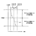
- FIG. 14 is a diagram showing a configuration of a conventional gradation voltage generation circuit (liquid crystal driving power supply circuit) disclosed in Patent Document 1.
- the gradation voltage generation circuit shown in FIG. 14 is configured to use voltages V1 to V6 divided by frequency dividing resistors R1 to R6 as power supply voltages of the operational amplifiers (voltage followers) 200a to 200d.
- the grayscale voltage generation circuit shown in FIG. 14 is configured such that the voltage at the previous stage and the next stage among the voltages divided by the frequency dividing resistors R1 through R6 are used as the power supply voltages of the operational amplifiers 200a through 200d.
- the voltage V1 and the voltage V3 are supplied as power supply voltages to the operational amplifier 200a to which the voltage V2 is input.
- the configuration of Patent Document 1 has the following problems. As described above, the power supply voltage of each of the plurality of operational amplifiers is configured such that among the voltages divided by the plurality of frequency dividing resistors, the voltages at the previous stage and the next stage with respect to the input voltage of the operational amplifier are used. there.
- the power supply voltage of each of the plurality of operational amplifiers is configured such that among the voltages divided by the plurality of frequency dividing resistors, the voltages at the previous stage and the next stage with respect to the input voltage of the operational amplifier are used.
- the configuration of Patent Document 1 may cause breakdown of each transistor constituting the operational amplifier, but there is no suggestion or disclosure about the countermeasure.
- the present invention has been made to solve the above-described problems, and provides a grayscale voltage generation circuit capable of appropriately switching grayscale voltages and a display device using the same, together with downsizing. it is.
- a gradation voltage generating circuit configured to perform gradation of image data by dividing each voltage between a high potential side power source and a low potential side power source.
- a ladder resistor configured by connecting a plurality of resistors in series so as to generate a plurality of reference voltages in accordance with the reference voltage, and the reference voltage provided for each of the plurality of reference voltages is used as the gradation voltage.
- a voltage follower circuit group composed of a plurality of voltage follower circuits to be output, and a plurality of gradation voltages output from the voltage follower circuit group and the image data are input, and the gradation of the image data
- a gradation voltage selection circuit composed of a plurality of selection circuits configured to select and output one gradation voltage corresponding to the plurality of gradation voltages, and each of the plurality of selection circuits.
- the voltage follower circuit included in each of the voltage follower circuits is driven by different power supply voltages having a potential difference lower than the potential difference between the maximum voltage and the minimum voltage of the reference voltage, and the gradation voltage selection circuit
- the plurality of selection circuits are divided into two or more switch circuits, and the two or more switch circuits include the selection circuits belonging to each with a potential difference lower than a potential difference between a maximum voltage and a minimum voltage of the plurality of reference voltages.
- Each gray scale voltage selection is switched to an output path from each switch circuit to the output terminal.
- a precharge circuit configured to hold the output voltage at an intermediate voltage between a maximum voltage and a minimum voltage of the plurality of reference voltages in the process.
- the voltage follower circuit is configured by a transistor having a breakdown voltage corresponding to a power supply voltage having a potential difference lower than a potential difference between the maximum voltage and the minimum voltage of the plurality of reference voltages. It is good also as.
- the switch circuit is configured by a transistor having a withstand voltage corresponding to a power supply voltage having a potential difference lower than a potential difference between the maximum voltage and the minimum voltage of the plurality of reference voltages. it may be.
- the voltage follower circuit may be configured by an operational amplifier in which an output terminal is connected to an inverting input terminal and the reference voltage is input to a non-inverting input terminal.
- the intermediate voltage is an average voltage of the maximum voltage and the minimum voltage of the plurality of reference voltages. There may be.
- the plurality of voltage follower circuits included in the voltage follower circuit group and the plurality of selection circuits included in the gradation voltage selection circuit include the maximum voltage and the minimum voltage of the plurality of reference voltages generated by the ladder resistor. Since it is driven with a potential difference lower than that between and with a different power supply voltage having the lower potential difference, it is configured with a low breakdown voltage transistor as compared with the case where it is not so divided can do. Thereby, the area of the whole gradation voltage generating circuit can be suppressed.
- a plurality of voltage follower circuits included in the voltage follower circuit group and a plurality of selection circuits included in the gradation voltage selection circuit are configured by low breakdown voltage transistors, respectively.
- a voltage higher than the withstand voltage is applied to the transistor.
- the precharge circuit temporarily holds the voltage at the output terminal at an intermediate voltage between the maximum reference voltage and the minimum reference voltage generated by the ladder resistor. At most, a potential difference between the maximum reference voltage and the intermediate voltage or a potential difference between the intermediate voltage and the minimum reference voltage is applied.
- the low voltage transistor is not required to apply a potential difference between the maximum reference voltage and the minimum reference voltage. Thereby, the breakdown of the breakdown voltage of the low breakdown voltage transistor can be suppressed.
- the process of switching the selection of the grayscale voltage is a process of switching between the positive reference voltage and the negative reference voltage
- the selection circuit includes:
- the output path may further include a short circuit configured to hold the voltage at the output terminal at the ground potential in the process of switching the positive reference voltage and the negative reference voltage to each other.
- the voltage at the output terminal is grounded by a short circuit in the process of switching the positive reference voltage or the negative reference voltage to each other (polarity inversion). Since the potential is once held, the low withstand voltage transistor is applied with a potential difference between the maximum positive reference voltage and the ground potential or a potential difference between the ground potential and the minimum negative reference voltage. different. In other words, the potential difference between the positive maximum reference voltage and the negative minimum reference voltage is not applied to the low breakdown voltage transistor during polarity reversal. Thereby, the breakdown of the breakdown voltage of the low breakdown voltage transistor can be suppressed.
- an operational amplifier that outputs a gradation voltage near a boundary between the plurality of gradation voltage generation units among the plurality of operational amplifiers that respectively constitute the plurality of voltage follower circuits.
- the regulated voltage may be driven by a power supply voltage different from that of other operational amplifiers in which the regulated voltage is within the operable voltage range of the operational amplifier.
- the operational amplifier that outputs the gradation voltage near the boundary of the plurality of gradation voltage generation units among the plurality of operational amplifiers included in the voltage follower circuit group is driven within the operable voltage range. Normal output can be obtained.
- a display device includes a plurality of pixels arranged in a matrix and a plurality of pixels connected to the plurality of pixels for each column or row.
- a display panel comprising: a signal line; and a plurality of scanning lines for selecting, for each row or column, a pixel to which the gradation voltage is to be applied among the plurality of pixels, via the plurality of scanning lines
- a scanning line driving circuit for selecting the pixel, the gradation voltage generating circuit in which the plurality of output terminals are connected to the plurality of signal lines, and a gradation voltage corresponding to the image data are the plurality of pixels.
- a timing controller that controls output of the grayscale voltage from the plurality of output terminals by the grayscale voltage generation circuit and selection of the pixel by the scanning line driving circuit so as to be applied to it is.
- a gradation voltage generating circuit capable of appropriately switching gradation voltages together with downsizing and a display device using the same.
- FIG. 1 is a diagram showing a configuration example of a display device according to Embodiment 1 of the present invention.
- FIG. 2 is a diagram schematically showing the configuration of each pixel shown in FIG.
- FIG. 3 is a graph showing the relationship between image data and gradation voltage.
- FIG. 4 is a block diagram showing a configuration example of the gradation voltage generating circuit according to the first embodiment of the present invention.
- FIG. 5 is a diagram showing a configuration example of a selection circuit included in the gradation voltage selection circuit shown in FIG.
- FIG. 6 is a diagram showing another configuration example of the selection circuit included in the gradation voltage selection circuit shown in FIG.
- FIG. 7 is a waveform diagram for explaining the operation of the selection circuit shown in FIG. FIG.
- FIG. 8 is a block diagram showing a configuration example of a gradation voltage generating circuit configured by connecting a positive circuit and a negative circuit.
- FIG. 9 is a block diagram showing a configuration example of a selection circuit included in the gradation voltage selection circuit shown in FIG.
- FIG. 10 is a waveform diagram for explaining an operation example of the selection circuit shown in FIG.
- FIG. 11 is a block diagram showing a configuration example of the gradation voltage generating circuit according to the second embodiment of the present invention.
- FIG. 12 is a circuit diagram showing a configuration example of a general operational amplifier.
- FIG. 13 is a diagram for explaining an operable voltage range of the operational amplifier shown in FIG.
- FIG. 14 is a diagram showing a configuration of a conventional gradation voltage generation circuit (liquid crystal drive power supply circuit).
- FIG. 1 is a diagram showing a configuration example of a display device according to Embodiment 1 of the present invention. Note that throughout all of the following embodiments, a liquid crystal display device is cited as an example of a display device according to the present invention, but the present invention is not limited to this, and an active matrix (active matrix) in which gradation voltages are corrected according to gamma characteristics. ) Type display device.
- FIG. 2 is a diagram schematically showing the configuration of each pixel shown in FIG.
- FIG. 3 is a graph showing the relationship between image data and gradation voltage.
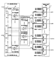
- the liquid crystal display device of FIG. 1 includes a liquid crystal panel 100, a backlight 110, a scanning line driving circuit 10, a signal line driving circuit 20, and a timing controller 30.
- Scanning line driving is performed so that display light is incident on the liquid crystal panel 100 from the backlight 110 and the display light is transmitted with a transmittance according to image data DATA (gradation data, display data) commanded from the outside.
- image data DATA gradient data, display data
- the liquid crystal panel 100 has a structure in which a liquid crystal layer 103 is sandwiched between a counter substrate 101 and an array substrate 102.
- a deflection plate 105 is disposed on the surface of the array substrate 102 and the counter substrate 101 opposite to the liquid crystal layer 103, and a light distribution film (not shown) is disposed on the surface of the array substrate 102 and the counter substrate 101 on the liquid crystal layer 103 side. Is arranged.
- N ⁇ M pixels PIX_ij (i 1) arranged in a matrix (here, N rows ⁇ M columns, where N and M are natural numbers, and so on).
- N, j 1 to M)
- the scanning line G_j is driven by the scanning line driving circuit 10
- the signal line Y_i is driven by the signal line driving circuit 20.
- a thin film transistor (TFT) W and a pixel electrode PIX are formed at the intersection of the scanning line G_j and the signal line Y_i.
- the thin film transistor (transistor) W has a gate connected to one scanning line G_j, a source connected to one signal line Y_i, and a drain connected to the pixel electrode PIX. Has been.
- the counter substrate 101 includes a color filter (not shown) disposed on the glass substrate and a common electrode VCOM disposed on the color filter so as to face the pixel electrode PIX of the array substrate 102.
- a liquid crystal capacitor C (including parasitic capacitance) is formed between the common electrode VCOM and the pixel electrode PIX facing the common electrode VCOM.
- the transmittance of the pixel PIX_ij is a difference voltage between the gradation voltage (pixel voltage) supplied to the pixel electrode PIX of the array substrate 102 and the common voltage supplied to the common electrode VCOM of the counter substrate 101 in the liquid crystal layer 103. It is controlled according to the applied driving voltage.
- the common electrode VCOM is connected to a power source for applying a common voltage via a common line (not shown) formed on the counter substrate 101.
- the signal line drive circuit 20 includes a gradation voltage generation circuit 40 and an output circuit 50.
- the output circuit 50 buffers the grayscale voltage supplied from the grayscale voltage generation circuit 40 for each signal line Y_i, and outputs it to each signal line Y_i. Thereby, each of the plurality of signal lines Y_i is driven.
- the timing controller 30 outputs the grayscale voltage outputs ⁇ 1 to ⁇ 64 from the grayscale voltage generation circuit 40 and the pixels from the scanning line drive circuit 10 so that the grayscale voltages ⁇ 1 to ⁇ 64 corresponding to the image data DATA are applied to the pixels PIX_ij.
- Controls selection of PIX_ij For example, the control signal CTG for sequentially selecting the scanning lines G_1 to G_N every one vertical scanning period (1V) and the analog for the pixel PIX_ij for one line included in the image data DATA every one horizontal scanning period (1H).
- a control signal CTY for assigning the image data DATA to each of the signal lines Y_1 to Y_M is generated.
- the control signal CTG includes a vertical start signal which is a pulse generated every one vertical scanning period (1V), a vertical clock signal which is a pulse generated for the number of scanning lines G_j in one vertical scanning period (1V), and the like. And is supplied from the timing controller 30 to the scanning line driving circuit 10.
- the control signal CTY includes a horizontal start signal STH which is a pulse generated every horizontal scanning period (1H), a horizontal clock signal CKH which is a pulse generated by the number of signal lines in each horizontal scanning period, and pixels for one line.
- a strobe signal STB which is a pulse generated with a predetermined time delay from the start signal STH every horizontal scanning period (1H), and every horizontal scanning period (1H) and a polarity signal POL for setting the polarity of the pixel voltage with respect to the common voltage VCOM every vertical scanning period (1V).
- the control signal CTY is supplied from the timing controller 30 to the signal line driving circuit 20 together with the image data DATA.
- the image data DATA includes gradation data for correcting gradation characteristics (gamma characteristics) of the liquid crystal panel 100.
- FIG. 4 is a block diagram showing a configuration example of the gradation voltage generation circuit according to the first embodiment of the present invention.
- the image data DATA has 6 bits
- the gradation level has voltage levels corresponding to 64 types of gradations, which is the sixth power of 2.
- the ladder resistor 1 includes 65 resistors R1 to R65 between a high-potential-side power supply VDD and a low-potential-side power supply VSS generated based on a power supply voltage supplied from a power supply circuit (not shown). It is configured to be connected in series.
- the ladder resistor 1 divides the potential difference between the high-potential-side power supply VDD and the low-potential-side power supply VSS by the resistors R1 to R65, thereby taking out the reference voltages ⁇ ref1 to ⁇ ref64 from the connection points of the resistors R1 to R65.
- the reference voltage ⁇ ref1 is the maximum reference voltage
- the reference voltage ⁇ ref64 is the minimum reference voltage.
- one operational amplifier (2_1 to 2_64) is provided for each of the reference voltages ⁇ ref1 to ⁇ ref64 generated by the ladder resistor 1.
- Each of the operational amplifiers 2_1 to 2_64 is configured to be a voltage follower circuit. That is, the operational amplifiers 2_1 to 2_64 receive the reference voltages ⁇ ref1 to ⁇ ref64 from the ladder resistor 1, and output the gradation voltages ⁇ 1 to ⁇ 64 by impedance conversion so that the loss can be suppressed even when the input impedance of the external load is low. Is configured to do.
- the plurality of voltage follower circuits of the voltage follower circuit group 2 may be configured by a transistor amplifier circuit such as a source follower in addition to the operational amplifier.
- the gradation voltage selection circuit 3 is configured such that one selection circuit (3_1 to 3_M) is provided for each of the output terminals OUT1 to OUTM corresponding to the number of signal lines Y_i.
- the selection circuits 3_1 to 3_M are configured to select only one voltage to be applied to the pixels PIX_ij connected to the output terminals OUT1 to OUTM from the gradation voltages ⁇ 1 to ⁇ 64.
- the selection circuits 3_1 to 3_M receive the gradation voltages ⁇ 1 to ⁇ 64 from the voltage follower circuit group 2 and the 6-bit image data DATA from the timing controller 6, and the 6-bit image data. Based on the result of decoding DATA, one of the gradation voltages ⁇ 1 to ⁇ 64 is selected and output.
- the grayscale voltage generation circuit 40 shown in FIG. 4 makes the ladder resistor 1 and the voltage follower circuit group 2 at least two lower than the potential difference between the maximum reference voltage ⁇ ref1 and the minimum reference voltage ⁇ ref64. It is configured to be divided into two power systems.
- the gradation voltage generation circuit 40 includes a first gradation voltage generation unit 12_D1 that outputs any one of the gradation voltages ⁇ 1 (for example, 9.8 V) to ⁇ 32 (for example, 5.05 V),
- the second gradation voltage generator 12_D2 that outputs any one of the regulated voltages ⁇ 33 (for example, 5V) to ⁇ 64 (for example, 0.2V) is configured.
- the first power supply voltage for example, 10V
- the second power supply for generating the gradation voltages ⁇ 1 (9.8V above) to ⁇ 32 (5.05V above)
- a voltage for example, 4V
- the first power supply voltage and the second power supply voltage are generated based on a predetermined node voltage (VDD, ⁇ ref1 to ⁇ ref64, or VSS) of the ladder resistor 1 and drive the operational amplifiers 2_1 to 2_32. Used as
- the third power supply voltage (for example, 6V) and the fourth power supply voltage (for example, 0V) for generating the gradation voltages ⁇ 33 (5V) to ⁇ 64 (0.2V) are provided. It is used.
- the third power supply voltage and the fourth power supply voltage are generated based on a predetermined node voltage (VDD, ⁇ ref1 to ⁇ ref64, or VSS) of the ladder resistor 1 and drive the operational amplifiers 2_33 to 2_64. Used as
- the voltage follower circuit group 2 when the maximum gradation voltage ⁇ 1 is 9.8V, the voltage follower circuit group 2 needs to be configured using, for example, a 10V withstand voltage transistor exceeding 9.8V.
- the voltage follower circuit group 2 is divided into a first grayscale voltage generator 12_D1 and a second grayscale voltage generator 12_d2 each using a 6V power supply system. .
- the voltage follower circuit group 2 can be composed of transistors having a 6V breakdown voltage lower than the 10V breakdown voltage, and the area of the voltage follower circuit group 2 can be reduced accordingly.
- FIG. 5 is a diagram showing a configuration example of one selection circuit 3_1 included in the gradation voltage selection circuit 3 shown in FIG.
- the other selection circuits 3_2 to 3_M have the same configuration.
- the selection circuit 3_1 is configured by arranging a switch composed of a P-type transistor or an N-type transistor so as to realize a tournament-type selection algorithm.
- the tournament method selection algorithm is to repeatedly select two adjacent gradation voltages out of 64 gradation voltages based on the bit value of the image data DATA. It means an algorithm that finally selects one gradation voltage.
- the selection circuit 3_1 selects the gradation voltage ⁇ 64 input to the input terminal 64 and outputs it from the output terminal OUT1.
- the selection circuit 3_1 is configured to be divided into at least two power supply voltage systems according to the potential difference between the maximum reference voltage ⁇ ref1 and the minimum reference voltage ⁇ ref64.
- the selection circuit 3_1 includes a first switch circuit 3_D1 that outputs any one of gradation voltages ⁇ 1 (for example, 9.8V) to ⁇ 32 (for example, 5.05V), and a gradation voltage ⁇ 33 (for example, 5V). ) To ⁇ 64 (for example, 0.2V), and the second switch circuit 3_D2 that outputs any one of them is configured.
- the first power supply voltage (for example, 10V) and the second power supply voltage (for example, 10V) for generating the gradation voltages ⁇ 1 (9.8V described above) to ⁇ 32 (5.05V described above) are provided. 4V) is used.
- the first power supply voltage and the second power supply voltage are generated based on a predetermined node voltage (VDD, ⁇ ref1 to ⁇ ref64, or VSS) of the ladder resistor 1 and used as a power supply voltage for driving the switch. .
- the first power supply voltage is applied to the back gate of the P-type transistor used in the first switch circuit 3_D1
- the second gate is applied to the back gate of the N-type transistor used in the first switch circuit 3_D1.
- the power supply voltage is applied.
- a third power supply voltage for example, 6V
- a fourth power supply voltage for example, 0V
- the third power supply voltage and the fourth power supply voltage are generated based on a predetermined node voltage (VDD, ⁇ ref1 to ⁇ ref64, or VSS) of the ladder resistor 1 and used as a power supply voltage for driving the switch. .
- the third power supply voltage is applied to the back gate of the P-type transistor used in the second switch circuit 3_D2
- the fourth gate is applied to the back gate of the N-type transistor used in the second switch circuit 3_D2.
- the power supply voltage is applied.
- the selection circuit 3_1 when the maximum gradation voltage ⁇ 1 is 9.8V, the selection circuit 3_1 needs to be configured using, for example, a 10V withstand voltage transistor exceeding 9.8V.
- the selection circuit 3_1 is divided into a first switch circuit 3_D1 and a second switch circuit 3_d2 each using a 6V power supply system. Therefore, the selection circuit 3_1 can be formed of a transistor with a 6V breakdown voltage that is lower than the 10V breakdown voltage, and its area can be reduced.
- the maximum gradation voltage ⁇ 1 is connected between the source and drain of the output transistor of the operational amplifier 2_64. And a potential difference between the minimum gradation voltage ⁇ 64 is applied.
- the pixel capacitor C is divided into the maximum gradation voltage ⁇ 1 (9.8V) and the minimum gradation voltage ⁇ 64 (0.
- a method of once precharging to an intermediate voltage between 2V) is adopted.
- the intermediate voltage is 9.8V for the maximum gradation voltage ⁇ 1 and 0.2V for the minimum gradation voltage ⁇ 64
- the intermediate voltage is the average voltage of the maximum gradation voltage ⁇ 1 and the minimum gradation voltage ⁇ 64.
- FIG. 6 is a diagram showing another configuration example of one selection circuit 3_1 included in the gradation voltage selection circuit 3 shown in FIG. 4, that is, a configuration example for realizing the precharge of the pixel capacitor C.
- the selection circuit 3_1 shown in FIG. 6 is different from the selection circuit 3_1 shown in FIG. 5 in that precharge switches (precharge switches) 3_SW1 and 3_SW3 for temporarily holding the voltage at the output terminal OUT1 at an intermediate voltage when the grayscale voltage is switched. Is added.
- the complementary switch of the first switch circuit 3_D1 corresponding to the fifth bit of the 6-bit image data DATA is represented by 3_D1_SW1 (P-type transistor) and 3_D1_SW2 (N-type transistor), and is also 5 of the image data DATA.
- the complementary switch of the second switch circuit 3_D2 corresponding to the bit number is represented as 3_D2_SW1 (P-type transistor) and 3_D2_SW2 (N-type transistor).
- complementary switches corresponding to the sixth bit of the image data DATA are represented as 3_SW2 (P-type transistor) and 3_SW4 (N-type transistor).
- One end of the precharge switch 3_SW1 is connected between the output end of the fifth bit complementary switch 3_D1_SW1, 3_D1_SW2 on the first switch circuit 3_D1 side and the input end of the sixth bit switch 3_SW2, and the other end. Is configured so that an intermediate voltage is applied thereto.
- One end of the precharge switch 3_SW3 is connected between the output end of the fifth bit complementary switch 3_D2_SW1, 3_D2_SW2 on the second switch circuit 3_D2 side and the input end of the sixth bit switch 3_SW4, and the other end. Is configured so that an intermediate voltage is applied thereto.
- FIG. 7 is a waveform diagram for explaining the operation of the selection circuit 3_1 shown in FIG.
- the example of FIG. 6 illustrates an example in which the selection circuit 3_1 in FIG. 6 selects the minimum gradation voltage ⁇ 64 output from the operational amplifier 2_64 from the state where the maximum gradation voltage ⁇ 1 output from the operational amplifier 2_1 has been selected. ing.
- the operational amplifier 2_1 outputs the maximum gradation voltage ⁇ 1, on the first switch circuit 3_D1 side, the fifth bit switch 3_D1_SW1 is ON, the switch 3_D1_SW2 is OFF, the precharge switch 3_SW1 is OFF, In addition, it is assumed that the 6th bit switch 3_SW2 is in the ON state. On the second switch circuit 3_D2 side, it is assumed that the 5th bit switch 3_D2_SW1 and the switch 3_D2_SW2 are both OFF, the precharge switch 3_SW3 is ON, and the 6th bit switch 3_SW4 is OFF.
- the 5th bit switch 3_D1_SW1 is switched from the ON state to the OFF state, and the precharge switch 3_SW1 is switched from the OFF state to the ON state.
- the pixel capacitor C of the signal line Y_i connected to the output terminal OUT1 is charged to an intermediate voltage via the precharge switch 3_SW1 and the sixth bit switch 3_SW2.
- the 6th bit switch 3_SW2 switches from the ON state to the OFF state
- the precharge switch 3_SW3 switches from the ON state to the OFF state
- the bit switch 3_SW4 is switched from the OFF state to the ON state.
- the gradation voltage ⁇ 64 output from the operational amplifier 2_64 is changed to the fifth bit switch 3_D2_SW2, the sixth bit. Output from the output terminal OUT1 via the switch 3_SW4.
- the pixel connected to the signal line Y_i is charged before the minimum gradation voltage ⁇ 64 is charged from the operational amplifier 2_64.
- the capacitor C is charged with an intermediate voltage of 5 V via the precharge switch 3_SW1.
- the switch 3_D2_SW2 of the fifth bit is switched from the OFF state to the ON state, an intermediate voltage of 5 V is applied to the drain, and the source of the gradation voltage ⁇ 64 is 0. .2V is applied.
- the second switch circuit 3_D2 which is composed of a 6V withstand voltage transistor, and thus the operational amplifier 2_64 are reliably protected. Also for the switches 3_D1_SW1 and 3_D1_SW2, the precharge switch 3_SW1 continues to be ON while the minimum gradation voltage ⁇ 64 is output, so that the switches 3_D1_SW1 and 3_D1_SW2 are reliably protected.
- the liquid crystal display device is normally configured to alternately perform positive output that is positive with respect to the common voltage VCOM or negative output that is negative with respect to the common voltage VCOM. Has been.
- FIG. 8 is a block diagram showing a configuration example of a gradation voltage generation circuit configured by connecting a positive circuit and a negative circuit.
- 8 includes a first gradation voltage generator 12_D1, a second gradation voltage generator 12D2, and a gradation voltage selection circuit 3, and these components are illustrated in FIG. 4 are the same as those shown in FIG.
- the negative electrode circuit of FIG. 8 includes a first negative gradation voltage generation unit N12_D1, a second negative gradation voltage generation unit N12_D2, and a negative gradation voltage selection circuit N3.
- the voltage VCOM as a reference, a reverse polarity voltage that is line-symmetric with respect to the output terminals OUT1 to OUNM of the positive circuit is output.
- the output terminals OUT1 to OUTM of the positive circuit and the output terminals OUT1 to OUTM of the negative circuit are short-circuited.
- FIG. 9 is a block diagram showing a configuration example of the selection circuit 3_1 included in the gradation voltage selection circuits 3 and N3 shown in FIG.
- the other selection circuits 3_2 to 3_M have the same configuration.
- the transistors (particularly the switches 3_SW1 to SW4_SW4) constituting the gradation voltage selection circuits 3 and N3 are low breakdown voltage (for example, 10V breakdown voltage) transistors, so that the gradation voltage selection circuits 3 and N3 The area is reduced.
- the low breakdown voltage transistor may break down. For example, when the pixel capacitance C of the signal line of the liquid crystal panel 100 is charged with ⁇ 9.8 V (N ⁇ 64) at the time of negative electrode driving, +9.8 V ( ⁇ 1) at the time of positive electrode driving is newly added to the pixel capacitance C.
- the source-drain voltage of the switch 3_SW2 is 19.6V, and if the switch 3_SW2 is formed of, for example, a 10V breakdown voltage transistor, the breakdown voltage may be destroyed.
- the selection circuit 3 uses a short switch (short switch) 3_SW5 to short-circuit the output path to the ground potential GND. 6 has been added.
- FIG. 10 is a waveform diagram for explaining an operation example of the selection circuit 3_1 shown in FIG.
- the output is switched from ⁇ 9.8 V to the ground potential GND, and the charging voltage of the pixel capacitor C of the signal line Y_i of the liquid crystal panel 100 becomes 0 V.
- the open switch 3_SW6 is switched from the ON state to the OFF state.
- the short switch 3_SW5 is switched from the ON state to the OFF state, and the open switch 3_SW6 is switched from the OFF state to the ON state.
- the charging voltage of the pixel capacitor C is once maintained at 0 V as a stage before the gradation voltage ⁇ 1 output from the operational amplifier 2_1 is charged to the pixel capacitor C at the time of polarity inversion. That is, immediately after the switch 3_SW2 is turned on, 0 V is applied to its drain and 9.8 V ( ⁇ 1) is applied to its source. Therefore, the source-drain voltage of the switch 3_SW2 is suppressed from 19.6V to 9.8V, and when the switch 3_SW2 is formed of, for example, a 10V breakdown voltage transistor, there is no possibility of breakdown breakdown.
- FIG. 11 is a block diagram showing a configuration example of the gradation voltage generating circuit according to the second embodiment of the present invention.
- the grayscale voltage generation circuit shown in FIG. 11 is different from the configuration of the grayscale voltage generation circuit 40 shown in FIG. 4 in that the first of the plurality of grayscale voltages ⁇ 1 to ⁇ 64 is selected from the voltage follower circuit group 2A.
- Grayscale voltage close to the second power supply voltage of the second grayscale voltage generator 12D1A and the third power supply voltage of the second grayscale voltage generator 12_D2A (close to the boundary between the two power supply systems)
- boundary operational amplifiers One or a plurality of operational amplifiers (hereinafter referred to as boundary operational amplifiers) that output a regulated voltage are extracted, and the power supply voltage of the boundary operational amplifier is made independent of the voltage follower circuit group 2A.
- the boundary operational amplifier that outputs the boundary gradation voltage is operated near the power supply voltage, and there is a possibility that the operable voltage range may be out of range. Therefore, in the second embodiment, a boundary gradation voltage generation unit 12_D3A configured by a boundary operational amplifier whose power supply voltage is independent from the voltage follower circuit group 2A is newly added.
- the boundary gradation voltage generator 12_D3A generates a boundary gradation voltage close to the second power supply voltage and the third power supply voltage, and includes a boundary voltage follower circuit group 2A2.
- the boundary voltage follower circuit group 2A2 is composed of a plurality of boundary operational amplifiers (2_32, 2_33, etc.) that output boundary gradation voltages ( ⁇ 32, ⁇ 33, etc.).
- the boundary operational amplifiers include first to fourth power supply voltages.
- a fifth power supply voltage and a sixth power supply voltage that are independent from each other are supplied.
- the fifth power supply voltage is a voltage near the middle between the first power supply voltage and the second power supply voltage
- the sixth power supply voltage is a voltage near the middle between the third power supply voltage and the fourth power supply voltage. It is said.
- the gradation voltage output from the boundary voltage follower circuit group 2A2 falls within the voltage near the center of the operable voltage range, and the operation of the boundary voltage follower circuit group 2A2 is stabilized.
- the fifth power supply voltage and the sixth power supply voltage are not provided with a new ladder resistor, but reference voltages ( ⁇ ref5 (7.4 V), ⁇ ref59 (2) generated by the existing ladder resistor 1 are used. .7V) etc.) is used effectively. Thereby, an increase in the area of the gradation voltage generation circuit can be suppressed.
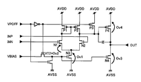
- FIG. 12 is a circuit diagram showing a configuration example of a general operational amplifier
- FIG. 13 is a diagram for explaining an operable voltage range of the operational amplifier shown in FIG.
- a general operational amplifier has, as its differential amplifying unit, P-type transistors P1 and P2 constituting a current mirror, and N-type transistors N1 and N2 provided on the current discharge side of the current mirror. And an N-type transistor N3 connected in common with the N-type transistors N1 and N2.
- a general operational amplifier has a P-type transistor P3 and an N-type transistor N4 connected in series as its output section.
- the ON voltage of the N-type transistor N3 is Ov1
- the ON voltage of the N-type transistor N1 is Ov2
- the ON voltage of the N-type transistor N4 is Ov3
- the ON voltage of the P-type transistor P3 is Ov4
- the input bias voltage is VT2.
- a voltage range in which the operational amplifier can operate is determined.
- the input potential difference of the operational amplifier configured as shown in FIG. 12 is in the range of [Ov1 + VT2 + Ov2 to AVDD]. Even if a voltage within the range of [AVSS to Ov1 + VT2 + Ov2] deviating from the input potential difference is input to the operational amplifier, the transistors constituting the operational amplifier operate in the non-saturated region, so that the operational amplifier cannot operate normally. Further, the output potential difference of the operational amplifier configured as shown in FIG.
- the boundary gradation voltages close to the second power supply voltage and the third power supply voltage are the boundary levels to which the fifth power supply voltage and the sixth power supply voltage independent of the first to fourth power supply voltages are applied. It was made to generate in the regulated voltage generator 12_D3A.
- the fifth power supply voltage may be approximately 7.5 V in the vicinity of the middle between the first power supply voltage and the second power supply voltage, and the sixth power supply voltage is the same as the third power supply voltage. What is necessary is just to give the voltage of about 2.5V in the middle of the fourth power supply voltage.
- the gradation voltage circuit and the display device using the same according to the present invention are particularly useful for a liquid crystal display device used in an electronic device such as a notebook personal computer that is required to be compact and have high performance.
- DESCRIPTION OF SYMBOLS 10 ... Scanning line drive circuit 20 ... Signal line drive circuit 30 ... Timing controller 40 ... Gradation voltage generation circuit 50 ... Output circuit 100 ... Liquid crystal panel 101 ... Counter substrate 102 ... Array substrate 103 ... Liquid crystal layer 105 ... Deflection plate 110 ... Back Lights OUT1 to OUTM ... Output terminals Y_1 to Y_N ... Signal lines G_1 to G_N ... Scanning lines 12_D1, N12_D1 ... First gradation voltage generators 12_D2, N12_D2 ... Second gradation voltages generator 1 ...
- Ladder resistors R1 to R65 frequency dividing resistors ⁇ ref1 to ⁇ ref64: reference voltage 2, 2A: voltage follower circuit group 3, N3: gradation voltage selection circuit ⁇ 1 to ⁇ 64: gradation voltage (positive output) N ⁇ 1 to N ⁇ 64 ... gradation voltage (negative output) 3_1 to 3_M... Selection circuit 3_D1... First switch circuit 3_D2... Second switch circuit 3_SW1, 3_SW2... Precharge switch 3_SW5.
Landscapes
- Engineering & Computer Science (AREA)
- Chemical & Material Sciences (AREA)
- Crystallography & Structural Chemistry (AREA)
- Physics & Mathematics (AREA)
- Computer Hardware Design (AREA)
- General Physics & Mathematics (AREA)
- Theoretical Computer Science (AREA)
- Control Of Indicators Other Than Cathode Ray Tubes (AREA)
- Liquid Crystal (AREA)
- Liquid Crystal Display Device Control (AREA)
Abstract
This gradient voltage generating circuit is configured such that a plurality of voltage follower circuits (2_1~2_64) are divided between at least two gradient voltage generating units (12_D1, 12_D2), and the two or more gradient voltage generating units drive the respective voltage follower circuit included therein at different power supply voltages having a lower potential difference than the potential difference between the maximum voltage (γref1) and the minimum voltage (γref64) among a plurality of reference voltages. A plurality of selection circuits (3_1~3_M) are also similarly divided between at least two switch circuits (3_D1, 3_D2), and driven. Furthermore, a pre-charge circuit can be further provided in the output path from the switch circuit to an output terminal, said pre-charge circuit being configured such that, by means of a process for changing the gradient voltage selection, the output terminal voltage is maintained at an intermediate voltage which is between the maximum and minimum voltages among the plurality of reference voltages.
Description
本発明は、階調電圧発生回路及びそれを用いた表示装置に関する。
The present invention relates to a gradation voltage generation circuit and a display device using the same.
近年、小型化かつ高精細化が進んでいるTFT(Thin Film Transistor)を使用したアクティブマトリックス(active matrix)型の液晶パネルでは、多階調化による色調豊富でかつ高画質な画像表示が要求されている。このような要求を満たすために、画像データに応じた階調電圧がガンマ特性に応じて補正され、該補正された階調電圧によって液晶パネルの信号線(ソース線又はデータ線とも呼ばれる)が駆動されている。なお、階調電圧の補正は、一般的に、複数の抵抗を直列に接続して構成されたラダー抵抗器を含む階調電圧発生回路により行われる。
In recent years, active matrix type liquid crystal panels using TFTs (Thin Film Transistors), which are becoming smaller and more precise, are required to display images with abundant colors and high image quality through multi-gradation. ing. In order to satisfy such a requirement, the gradation voltage corresponding to the image data is corrected according to the gamma characteristic, and the signal line (also referred to as a source line or data line) of the liquid crystal panel is driven by the corrected gradation voltage. Has been. Note that the correction of the gradation voltage is generally performed by a gradation voltage generation circuit including a ladder resistor configured by connecting a plurality of resistors in series.
図14は、特許文献1に示された従来の階調電圧発生回路(液晶駆動電源回路)の構成を示した図である。図14に示す階調電圧発生回路は、オペアンプ(ボルテージフォロワ)200a~200dそれぞれの電源電圧として分周抵抗R1~R6により分周された電圧V1~V6を用いるように構成されている。特に、図14に示す階調電圧発生回路は、オペアンプ200a~200dそれぞれの電源電圧として、分周抵抗R1~R6により分周された電圧のうち前段及び次段の電圧が用いられるように構成されている。例えば、電圧V2が入力されるオペアンプ200aに対して電圧V1及び電圧V3が電源電圧として供給される。
FIG. 14 is a diagram showing a configuration of a conventional gradation voltage generation circuit (liquid crystal driving power supply circuit) disclosed in Patent Document 1. In FIG. The gradation voltage generation circuit shown in FIG. 14 is configured to use voltages V1 to V6 divided by frequency dividing resistors R1 to R6 as power supply voltages of the operational amplifiers (voltage followers) 200a to 200d. In particular, the grayscale voltage generation circuit shown in FIG. 14 is configured such that the voltage at the previous stage and the next stage among the voltages divided by the frequency dividing resistors R1 through R6 are used as the power supply voltages of the operational amplifiers 200a through 200d. ing. For example, the voltage V1 and the voltage V3 are supplied as power supply voltages to the operational amplifier 200a to which the voltage V2 is input.
特許文献1の構成では、次のような問題がある。上記のとおり、複数のオペアンプそれぞれの電源電圧として、複数の分周抵抗により分周された電圧のうち、該オペアンプの入力電圧に対して前段及び次段となる電圧が用いられるように構成されている。しかしながら、液晶パネルの運用上、複数のオペアンプから出力される複数の階調電圧のうち一つが選択されるとき、信号線を介して画素容量に印加されることになる。このため、階調電圧が切り替えられる時、オペアンプを構成する各トランジスタには前段及び次段の電圧間の電位差よりも高い電位差が印加される場合がある。従って、特許文献1の構成では、オペアンプを構成する各トランジスタの耐圧破壊を引き起こしかねないが、その対策について何ら示唆も開示もされていない。
The configuration of Patent Document 1 has the following problems. As described above, the power supply voltage of each of the plurality of operational amplifiers is configured such that among the voltages divided by the plurality of frequency dividing resistors, the voltages at the previous stage and the next stage with respect to the input voltage of the operational amplifier are used. there. However, in the operation of the liquid crystal panel, when one of a plurality of gradation voltages output from a plurality of operational amplifiers is selected, it is applied to the pixel capacitor via a signal line. For this reason, when the gradation voltage is switched, a potential difference higher than the potential difference between the voltage at the previous stage and the next stage may be applied to each transistor constituting the operational amplifier. Therefore, the configuration of Patent Document 1 may cause breakdown of each transistor constituting the operational amplifier, but there is no suggestion or disclosure about the countermeasure.
本発明の目的は、上記問題点を解決するためになされたもので、小型化と併せて階調電圧の切り替えを適切に遂行可能な階調電圧発生回路及びそれを用いた表示装置を提供することである。
SUMMARY OF THE INVENTION The present invention has been made to solve the above-described problems, and provides a grayscale voltage generation circuit capable of appropriately switching grayscale voltages and a display device using the same, together with downsizing. it is.
上記の課題を解決するために、本発明の一つの形態(aspect)に係る階調電圧発生回路は、高電位側電源と低電位側電源との間にそれぞれの分圧により画像データの階調に応じた複数の基準電圧を発生するように複数の抵抗が直列に接続されて構成されたラダー抵抗器と、前記複数の基準電圧毎に設けられ、入力される前記基準電圧を前記階調電圧として出力する複数のボルテージフォロワ回路から成るボルテージフォロワ回路群と、前記ボルテージフォロワ回路群から出力された複数の前記階調電圧が入力されるとともに前記画像データが入力されて、該画像データの階調に対応する一つの階調電圧を該複数の階調電圧の中から選択して出力するように構成された複数の選択回路から成る階調電圧選択回路と、前記複数の選択回路にそれぞれ接続された複数の出力端と、を備え、前記ボルテージフォロワ回路群の前記複数のボルテージフォロワ回路は二以上の階調電圧発生部に区分され、且つ前記二以上の階調電圧発生部は前記複数の基準電圧の最大電圧と最小電圧との間の電位差よりも低い電位差を有した互いに異なる電源電圧でそれぞれに含まれる前記ボルテージフォロワ回路をそれぞれ駆動するよう構成され、前記階調電圧選択回路の前記複数の選択回路は二以上のスイッチ回路に区分され、且つ前記二以上のスイッチ回路は前記複数の基準電圧の最大電圧と最小電圧との間の電位差よりも低い電位差でそれぞれに属する前記選択回路をそれぞれ駆動するよう構成され、且つ それぞれの前記スイッチ回路から前記出力端に至る出力経路には、前記階調電圧の選択を切り替える過程で、前記出力端の電圧を前記複数の基準電圧の最大電圧と最小電圧との間の中間電圧に保持させるように構成されたプリチャージ回路をさらに備える、ものである。
In order to solve the above problem, a gradation voltage generating circuit according to one aspect of the present invention is configured to perform gradation of image data by dividing each voltage between a high potential side power source and a low potential side power source. A ladder resistor configured by connecting a plurality of resistors in series so as to generate a plurality of reference voltages in accordance with the reference voltage, and the reference voltage provided for each of the plurality of reference voltages is used as the gradation voltage. A voltage follower circuit group composed of a plurality of voltage follower circuits to be output, and a plurality of gradation voltages output from the voltage follower circuit group and the image data are input, and the gradation of the image data A gradation voltage selection circuit composed of a plurality of selection circuits configured to select and output one gradation voltage corresponding to the plurality of gradation voltages, and each of the plurality of selection circuits. A plurality of connected output terminals, wherein the plurality of voltage follower circuits of the voltage follower circuit group are divided into two or more gray voltage generators, and the two or more gray voltage generators are the plurality of gray voltage generators. The voltage follower circuit included in each of the voltage follower circuits is driven by different power supply voltages having a potential difference lower than the potential difference between the maximum voltage and the minimum voltage of the reference voltage, and the gradation voltage selection circuit The plurality of selection circuits are divided into two or more switch circuits, and the two or more switch circuits include the selection circuits belonging to each with a potential difference lower than a potential difference between a maximum voltage and a minimum voltage of the plurality of reference voltages. Each gray scale voltage selection is switched to an output path from each switch circuit to the output terminal. And a precharge circuit configured to hold the output voltage at an intermediate voltage between a maximum voltage and a minimum voltage of the plurality of reference voltages in the process.
前記階調電圧発生回路において、前記ボルテージフォロワ回路は、前記複数の基準電圧の最大電圧と最小電圧との間の電位差よりも低い電位差を有した電源電圧に応じた耐圧のトランジスタで構成されている、としてもよい。
In the gradation voltage generation circuit, the voltage follower circuit is configured by a transistor having a breakdown voltage corresponding to a power supply voltage having a potential difference lower than a potential difference between the maximum voltage and the minimum voltage of the plurality of reference voltages. It is good also as.
前記階調電圧発生回路において、前記スイッチ回路は、前記複数の基準電圧の最大電圧と最小電圧との間の電位差よりも低い電位差を有した電源電圧に応じた耐圧のトランジスタで構成されている、としてもよい。
In the gradation voltage generation circuit, the switch circuit is configured by a transistor having a withstand voltage corresponding to a power supply voltage having a potential difference lower than a potential difference between the maximum voltage and the minimum voltage of the plurality of reference voltages. it may be.
前記階調電圧発生回路において、前記ボルテージフォロワ回路が、反転入力端子に出力端子が接続され、且つ非反転入力端子に前記基準電圧が入力されるオペアンプで構成されている、としてもよい。
In the gradation voltage generating circuit, the voltage follower circuit may be configured by an operational amplifier in which an output terminal is connected to an inverting input terminal and the reference voltage is input to a non-inverting input terminal. *
前記階調電圧発生回路において、前記階調電圧発生部が二つであり、前記スイッチ回路が二つであり、且つ前記中間電圧は前記複数の基準電圧の最大電圧と最小電圧との平均電圧である、としてもよい。
In the gradation voltage generation circuit, there are two gradation voltage generation units, two switch circuits, and the intermediate voltage is an average voltage of the maximum voltage and the minimum voltage of the plurality of reference voltages. There may be.
この構成によれば、ボルテージフォロワ回路群に含まれる複数のボルテージフォロワ回路と階調電圧選択回路に含まれる複数の選択回路は、ラダー抵抗器で生成される複数の基準電圧の最大電圧と最小電圧との間の電位差よりも低い電位差で駆動されるとともに、該低い電位差を有した互いに異なる電源電圧で駆動されるように区分されるので、そのように区分しない場合と比べて低耐圧トランジスタで構成することができる。これにより、階調電圧発生回路全体の面積が抑えられる。
According to this configuration, the plurality of voltage follower circuits included in the voltage follower circuit group and the plurality of selection circuits included in the gradation voltage selection circuit include the maximum voltage and the minimum voltage of the plurality of reference voltages generated by the ladder resistor. Since it is driven with a potential difference lower than that between and with a different power supply voltage having the lower potential difference, it is configured with a low breakdown voltage transistor as compared with the case where it is not so divided can do. Thereby, the area of the whole gradation voltage generating circuit can be suppressed.
なお、ボルテージフォロワ回路群に含まれる複数のボルテージフォロワ回路と階調電圧選択回路に含まれる複数の選択回路とをそれぞれ低耐圧トランジスタで構成することに伴って、階調電圧の切り替え前後において低耐圧トランジスタには耐圧以上の電圧が印加される場合がある。しかしながら、階調電圧を切り替える過程で、プリチャージ回路によって出力端の電圧がラダー抵抗器で生成される最大基準電圧と最小基準電圧との間の中間電圧に一旦保持されるので、低耐圧トランジスタには最大でも最大基準電圧と中間電圧との間の電位差又は中間電圧と最小基準電圧との間の電位差が印加されることなる。言い換えると、階調電圧が切り替えられる時に、低耐圧トランジスタには最大基準電圧と最小基準電圧との間の電位差が印加されずに済むようになる。これにより、低耐圧トランジスタの耐圧破壊の発生を抑えることができる。
A plurality of voltage follower circuits included in the voltage follower circuit group and a plurality of selection circuits included in the gradation voltage selection circuit are configured by low breakdown voltage transistors, respectively. In some cases, a voltage higher than the withstand voltage is applied to the transistor. However, in the process of switching the grayscale voltage, the precharge circuit temporarily holds the voltage at the output terminal at an intermediate voltage between the maximum reference voltage and the minimum reference voltage generated by the ladder resistor. At most, a potential difference between the maximum reference voltage and the intermediate voltage or a potential difference between the intermediate voltage and the minimum reference voltage is applied. In other words, when the gradation voltage is switched, the low voltage transistor is not required to apply a potential difference between the maximum reference voltage and the minimum reference voltage. Thereby, the breakdown of the breakdown voltage of the low breakdown voltage transistor can be suppressed.
前記階調電圧発生回路において、前記階調電圧の選択を切り替える過程は、正極性の前記基準電圧と負極性の前記基準電圧とを相互に切り替える過程であり、前記選択回路は、前記スイッチ回路の出力経路に、正極性の前記基準電圧と負極性の前記基準電圧とを相互に切り替える過程で、前記出力端の電圧をグランド電位に保持させるように構成されたショート回路をさらに備える、としてもよい。
In the grayscale voltage generation circuit, the process of switching the selection of the grayscale voltage is a process of switching between the positive reference voltage and the negative reference voltage, and the selection circuit includes: The output path may further include a short circuit configured to hold the voltage at the output terminal at the ground potential in the process of switching the positive reference voltage and the negative reference voltage to each other. .
この構成によれば、表示パネルの焼きつき防止等のために、正極性の前記基準電圧又は負極性の前記基準電圧を相互に切り替える過程(極性反転)において、ショート回路によって出力端の電圧をグランド電位に一旦保持させることにしたので、低耐圧トランジスタには最大でも正極性の最大基準電圧とグランド電位との間の電位差又はグランド電位と負極性の最小基準電圧との間の電位差が印加されることなる。言い換えると、極性反転時に、低耐圧トランジスタには正極性の最大基準電圧と負極性の最小基準電圧との間の電位差が印加されずに済むようになる。これにより、低耐圧トランジスタの耐圧破壊の発生を抑えることができる。
According to this configuration, in order to prevent burn-in of the display panel or the like, the voltage at the output terminal is grounded by a short circuit in the process of switching the positive reference voltage or the negative reference voltage to each other (polarity inversion). Since the potential is once held, the low withstand voltage transistor is applied with a potential difference between the maximum positive reference voltage and the ground potential or a potential difference between the ground potential and the minimum negative reference voltage. different. In other words, the potential difference between the positive maximum reference voltage and the negative minimum reference voltage is not applied to the low breakdown voltage transistor during polarity reversal. Thereby, the breakdown of the breakdown voltage of the low breakdown voltage transistor can be suppressed.
前記階調電圧発生回路において、前記複数のボルテージフォロワ回路をそれぞれ構成する前記複数のオペアンプのうち前記複数の階調電圧発生部の境界付近の階調電圧を出力するオペアンプは、該境界付近の階調電圧が該オペアンプの動作可能な電圧範囲内となるような他のオペアンプとは異なる電源電圧で駆動される、としてもよい。
In the gradation voltage generation circuit, an operational amplifier that outputs a gradation voltage near a boundary between the plurality of gradation voltage generation units among the plurality of operational amplifiers that respectively constitute the plurality of voltage follower circuits. The regulated voltage may be driven by a power supply voltage different from that of other operational amplifiers in which the regulated voltage is within the operable voltage range of the operational amplifier.
この構成によれば、ボルテージフォロワ回路群に含まれる複数のオペアンプのうち複数の階調電圧発生部の境界付近の階調電圧を出力するオペアンプは、その動作可能な電圧範囲内で駆動されるので、正常な出力を得ることができる。
According to this configuration, the operational amplifier that outputs the gradation voltage near the boundary of the plurality of gradation voltage generation units among the plurality of operational amplifiers included in the voltage follower circuit group is driven within the operable voltage range. Normal output can be obtained.
上記の課題を解決するために、本発明のその他の形態(aspect)に係る表示装置は、行列状に配置された複数の画素と、前記複数の画素に列又は行毎に接続された複数の信号線と、前記複数の画素のうちの前記階調電圧を印加すべき画素を行又は列毎に選択するための複数の走査線と、を備える表示パネルと、前記複数の走査線を介して前記画素の選択を行う走査線駆動回路と、前記複数の信号線に前記複数の出力端がそれぞれ接続された前記階調電圧発生回路と、前記画像データに対応する階調電圧が前記複数の画素に印加されるように、前記階調電圧発生回路による前記複数の出力端からの前記階調電圧の出力と前記走査線駆動回路による前記画素の選択とを制御するタイミングコントローラと、を備える、ものである。
In order to solve the above problems, a display device according to another aspect of the present invention includes a plurality of pixels arranged in a matrix and a plurality of pixels connected to the plurality of pixels for each column or row. A display panel comprising: a signal line; and a plurality of scanning lines for selecting, for each row or column, a pixel to which the gradation voltage is to be applied among the plurality of pixels, via the plurality of scanning lines A scanning line driving circuit for selecting the pixel, the gradation voltage generating circuit in which the plurality of output terminals are connected to the plurality of signal lines, and a gradation voltage corresponding to the image data are the plurality of pixels. A timing controller that controls output of the grayscale voltage from the plurality of output terminals by the grayscale voltage generation circuit and selection of the pixel by the scanning line driving circuit so as to be applied to it is.
本発明によれば、小型化と併せて階調電圧の切り替えを適切に遂行可能な階調電圧発生回路及びそれを用いた表示装置を提供することができる。
According to the present invention, it is possible to provide a gradation voltage generating circuit capable of appropriately switching gradation voltages together with downsizing and a display device using the same.
以下、本発明の好ましい実施の形態を、図面を参照しながら説明する。なお、以下では全ての図を通じて同一又は相当する要素には同一の参照符号を付して、その重複する説明を省略する。
Hereinafter, preferred embodiments of the present invention will be described with reference to the drawings. In the following description, the same or corresponding elements are denoted by the same reference symbols throughout the drawings, and redundant description thereof is omitted.
(実施の形態1)
[表示装置]
図1は、本発明の実施の形態1に係る表示装置の構成例を示した図である。なお、以下の全ての実施の形態を通じて、本発明に係る表示装置として液晶表示装置を例に挙げているがこれに限られず、階調電圧がガンマ特性に応じて補正されるアクティブマトリックス(active matrix)型の表示装置であればよい。図2は、図1に示す各画素の構成を模式的に示した図である。図3は、画像データと階調電圧との関係を表したグラフである。 (Embodiment 1)
[Display device]
FIG. 1 is a diagram showing a configuration example of a display device according toEmbodiment 1 of the present invention. Note that throughout all of the following embodiments, a liquid crystal display device is cited as an example of a display device according to the present invention, but the present invention is not limited to this, and an active matrix (active matrix) in which gradation voltages are corrected according to gamma characteristics. ) Type display device. FIG. 2 is a diagram schematically showing the configuration of each pixel shown in FIG. FIG. 3 is a graph showing the relationship between image data and gradation voltage.
[表示装置]
図1は、本発明の実施の形態1に係る表示装置の構成例を示した図である。なお、以下の全ての実施の形態を通じて、本発明に係る表示装置として液晶表示装置を例に挙げているがこれに限られず、階調電圧がガンマ特性に応じて補正されるアクティブマトリックス(active matrix)型の表示装置であればよい。図2は、図1に示す各画素の構成を模式的に示した図である。図3は、画像データと階調電圧との関係を表したグラフである。 (Embodiment 1)
[Display device]
FIG. 1 is a diagram showing a configuration example of a display device according to
図1の液晶表示装置は、液晶パネル100と、バックライト(back light)110と、走査線駆動回路10と、信号線駆動回路20と、タイミングコントローラ(timing controller)30とを備えて構成されている。バックライト110から液晶パネル100に表示用の光が入射され、外部から指令された画像データDATA(階調データ、表示データ)に応じた透過率で表示用の光を透過するように走査線駆動回路10及び信号線駆動回路20が駆動されることにより、液晶パネル100に画像データDATAに応じた画像が表示される。
The liquid crystal display device of FIG. 1 includes a liquid crystal panel 100, a backlight 110, a scanning line driving circuit 10, a signal line driving circuit 20, and a timing controller 30. there. Scanning line driving is performed so that display light is incident on the liquid crystal panel 100 from the backlight 110 and the display light is transmitted with a transmittance according to image data DATA (gradation data, display data) commanded from the outside. By driving the circuit 10 and the signal line driving circuit 20, an image corresponding to the image data DATA is displayed on the liquid crystal panel 100.
液晶パネル100は、対向基板101とアレイ(array)基板102との間に液晶層103を挟持した構造となっている。アレイ基板102及び対向基板101における液晶層103とは反対側の表面には偏向板105が配置され、アレイ基板102及び対向基板101における液晶層103側の表面には配光膜(図示せず)が配置されている。
The liquid crystal panel 100 has a structure in which a liquid crystal layer 103 is sandwiched between a counter substrate 101 and an array substrate 102. A deflection plate 105 is disposed on the surface of the array substrate 102 and the counter substrate 101 opposite to the liquid crystal layer 103, and a light distribution film (not shown) is disposed on the surface of the array substrate 102 and the counter substrate 101 on the liquid crystal layer 103 side. Is arranged.
アレイ基板102の内面には、ガラス基板上に行列状(ここでは、N行×M列。但し、N、Mは自然数。以下同様)に配置されたN×M個の画素PIX_ij(i=1~N、j=1~M)と、画素PIX_ijに列又は行毎に接続されたN本の信号線Y_i(i=1~N)と、画素PIX_ijのうちの階調電圧を印加すべき画素を行又は列毎に選択するためのM本の走査線G_j(j=1~M)と、が形成されている。走査線G_jは走査線駆動回路10によって駆動され、信号線Y_iは信号線駆動回路20によって駆動される。
On the inner surface of the array substrate 102, N × M pixels PIX_ij (i = 1) arranged in a matrix (here, N rows × M columns, where N and M are natural numbers, and so on). N, j = 1 to M), N signal lines Y_i (i = 1 to N) connected to the pixel PIX_ij for each column or row, and a pixel to which the gradation voltage is to be applied among the pixels PIX_ij M scanning lines G_j (j = 1 to M) are selected for selecting for each row or column. The scanning line G_j is driven by the scanning line driving circuit 10, and the signal line Y_i is driven by the signal line driving circuit 20.
画素PIX_ijには、走査線G_j及び信号線Y_iの交差位置に、薄膜トランジスタ(TFT:Thin Film Transistor)W及び画素電極PIXが形成されている。薄膜トランジスタ(transistor)Wは、そのゲート(gate)が1本の走査線G_jに接続され、そのソース(source)が1本の信号線Y_iに接続され、そのドレイン(drain)が画素電極PIXに接続されている。
In the pixel PIX_ij, a thin film transistor (TFT) W and a pixel electrode PIX are formed at the intersection of the scanning line G_j and the signal line Y_i. The thin film transistor (transistor) W has a gate connected to one scanning line G_j, a source connected to one signal line Y_i, and a drain connected to the pixel electrode PIX. Has been.
対向基板101は、ガラス基板上に配置されたカラーフィルタ(図示せず)と、アレイ基板102の画素電極PIXに対向して該カラーフィルタ上に配置された共通電極VCOMとを含む。この共通電極VCOMとこれに対向する画素電極PIXとの間に液晶容量C(寄生容量も含む)が形成されている。画素PIX_ijの透過率は、アレイ基板102の画素電極PIXに供給される階調電圧(画素電圧)と、対向基板101の共通電極VCOMに供給されるコモン電圧と、の差電圧として液晶層103に印加される駆動電圧に応じて制御される。共通電極VCOMは対向基板101上に形成された共通線(図示せず)を介して、コモン電圧を付与する電源に接続されている。
The counter substrate 101 includes a color filter (not shown) disposed on the glass substrate and a common electrode VCOM disposed on the color filter so as to face the pixel electrode PIX of the array substrate 102. A liquid crystal capacitor C (including parasitic capacitance) is formed between the common electrode VCOM and the pixel electrode PIX facing the common electrode VCOM. The transmittance of the pixel PIX_ij is a difference voltage between the gradation voltage (pixel voltage) supplied to the pixel electrode PIX of the array substrate 102 and the common voltage supplied to the common electrode VCOM of the counter substrate 101 in the liquid crystal layer 103. It is controlled according to the applied driving voltage. The common electrode VCOM is connected to a power source for applying a common voltage via a common line (not shown) formed on the counter substrate 101.
信号線駆動回路20は、階調電圧発生回路40と、出力回路50とを含む。階調電圧発生回路40は、電源回路(図示せず)から供給された電源電圧をもとに複数の階調電圧を発生する。例えば1画素当たりの画像データDATAが6ビットの場合、64(=2の6乗)種類の階調電圧γ1~γ64を発生する(図3を参照)。また、階調電圧発生回路40は、信号線Y_iそれぞれを対象として、複数ビットの画像データDATAに基づいて複数の階調電圧のいずれか一つを選択して出力回路50に出力する。出力回路50は、信号線Y_iそれぞれを対象として、階調電圧発生回路40から供給された階調電圧をバッファリングして信号線Y_iそれぞれに出力する。これにより、複数の信号線Y_iそれぞれが駆動される。
The signal line drive circuit 20 includes a gradation voltage generation circuit 40 and an output circuit 50. The gradation voltage generation circuit 40 generates a plurality of gradation voltages based on a power supply voltage supplied from a power supply circuit (not shown). For example, when the image data DATA per pixel is 6 bits, 64 (= 2 to the sixth power) types of gradation voltages γ1 to γ64 are generated (see FIG. 3). Further, the gradation voltage generation circuit 40 selects one of the plurality of gradation voltages based on the plurality of bits of image data DATA and outputs the selected signal line Y_i to the output circuit 50. The output circuit 50 buffers the grayscale voltage supplied from the grayscale voltage generation circuit 40 for each signal line Y_i, and outputs it to each signal line Y_i. Thereby, each of the plurality of signal lines Y_i is driven.
タイミングコントローラ30は、画像データDATAに対応する階調電圧γ1~γ64が画素PIX_ijに印加されるように、階調電圧発生回路40による階調電圧の出力γ1~γ64と走査線駆動回路10による画素PIX_ijの選択とを制御する。例えば、1垂直走査期間(1V)毎に走査線G_1~G_Nを順次選択するための制御信号CTGと、1水平走査期間(1H)毎に画像データDATAに含まれる1ライン分の画素PIX_ijに対するアナログ画像データDATAを信号線Y_1~Y_Mそれぞれに割り当てるための制御信号CTYを発生する。
The timing controller 30 outputs the grayscale voltage outputs γ1 to γ64 from the grayscale voltage generation circuit 40 and the pixels from the scanning line drive circuit 10 so that the grayscale voltages γ1 to γ64 corresponding to the image data DATA are applied to the pixels PIX_ij. Controls selection of PIX_ij. For example, the control signal CTG for sequentially selecting the scanning lines G_1 to G_N every one vertical scanning period (1V) and the analog for the pixel PIX_ij for one line included in the image data DATA every one horizontal scanning period (1H). A control signal CTY for assigning the image data DATA to each of the signal lines Y_1 to Y_M is generated.
制御信号CTGは、1垂直走査期間(1V)毎に発生されるパルスである垂直スタート信号、及び1垂直走査期間(1V)において走査線G_jの本数分発生されるパルスである垂直クロック信号等を含み、タイミングコントローラ30から走査線駆動回路10に供給される。制御信号CTYは、1水平走査期間(1H)毎に発生されるパルスである水平スタート信号STH、各水平走査期間において信号線数分発生されるパルスである水平クロック信号CKH、1ライン分の画素PIX_ijに対する画像データDATAに対応して信号線Y_iを駆動するために1水平走査期間(1H)毎にスタート信号STHから所定時間遅れて発生されるパルスであるストローブ信号STB、及び1水平走査期間毎(1H)及び1垂直走査期間(1V)毎にコモン電圧VCOMに対して画素電圧の極性を設定するための極性信号POL等を含む。制御信号CTYは、画像データDATAと共にタイミングコントローラ30から信号線駆動回路20に供給される。なお、画像データDATAは、液晶パネル100の階調特性(ガンマ特性)を補正するための階調データを含む。
The control signal CTG includes a vertical start signal which is a pulse generated every one vertical scanning period (1V), a vertical clock signal which is a pulse generated for the number of scanning lines G_j in one vertical scanning period (1V), and the like. And is supplied from the timing controller 30 to the scanning line driving circuit 10. The control signal CTY includes a horizontal start signal STH which is a pulse generated every horizontal scanning period (1H), a horizontal clock signal CKH which is a pulse generated by the number of signal lines in each horizontal scanning period, and pixels for one line. In order to drive the signal line Y_i corresponding to the image data DATA for PIX_ij, a strobe signal STB which is a pulse generated with a predetermined time delay from the start signal STH every horizontal scanning period (1H), and every horizontal scanning period (1H) and a polarity signal POL for setting the polarity of the pixel voltage with respect to the common voltage VCOM every vertical scanning period (1V). The control signal CTY is supplied from the timing controller 30 to the signal line driving circuit 20 together with the image data DATA. The image data DATA includes gradation data for correcting gradation characteristics (gamma characteristics) of the liquid crystal panel 100. *
[階調電圧発生回路]
===ラダー(ladder)抵抗器及びボルテージフォロワ(voltage follower)回路群の低圧化===
図4は、本発明の実施の形態1に係る階調電圧発生回路の構成例を示したブロック図である。
[Grayscale voltage generator]
=== Lower pressure of ladder resistor and voltage follower circuit group ===
FIG. 4 is a block diagram showing a configuration example of the gradation voltage generation circuit according to the first embodiment of the present invention.
図4に示す階調電圧発生回路40は、ラダー抵抗器1と、ボルテージフォロワ回路群2と、階調電圧選択回路3とを含む。なお、同図に示す例では、画像データDATAが6ビットであり、階調電圧が2の6乗である64種類の階調に対応する電圧レベルを有する。
4 includes a ladder resistor 1, a voltage follower circuit group 2, and a gradation voltage selection circuit 3. The gradation voltage generation circuit 40 shown in FIG. In the example shown in the figure, the image data DATA has 6 bits, and the gradation level has voltage levels corresponding to 64 types of gradations, which is the sixth power of 2.
ラダー抵抗器1は、電源回路(図示せず)から供給された電源電圧をもとに生成された高電位側電源VDDと低電位側電源VSSとの間に、65個の抵抗R1~R65が直列に接続されて構成されている。ラダー抵抗器1は、高電位側電源VDDと低電位側電源VSSとの間の電位差を抵抗R1~R65により分圧することで、抵抗R1~R65それぞれの接続点から基準電圧γref1~γref64が取り出される。なお、基準電圧γref1が最大基準電圧であり、基準電圧γref64が最小基準電圧である。
The ladder resistor 1 includes 65 resistors R1 to R65 between a high-potential-side power supply VDD and a low-potential-side power supply VSS generated based on a power supply voltage supplied from a power supply circuit (not shown). It is configured to be connected in series. The ladder resistor 1 divides the potential difference between the high-potential-side power supply VDD and the low-potential-side power supply VSS by the resistors R1 to R65, thereby taking out the reference voltages γref1 to γref64 from the connection points of the resistors R1 to R65. . The reference voltage γref1 is the maximum reference voltage, and the reference voltage γref64 is the minimum reference voltage.
ボルテージフォロワ回路群2は、ラダー抵抗器1で生成した基準電圧γref1~γref64それぞれに対して1つのオペアンプ(2_1~2_64)が設けられている。オペアンプ2_1~2_64それぞれはボルテージフォロア回路となるように構成されている。つまり、オペアンプ2_1~2_64は、ラダー抵抗器1から基準電圧γref1~γref64が入力され、外部負荷の入力インピーダンスが低くても損失が抑えられるようにインピーダンス変換をして階調電圧γ1~γ64を出力するように構成されている。なお、ボルテージフォロワ回路群2の複数のボルテージフォロワ回路は、オペアンプで構成する他に、ソースフォロワ等のトランジスタ増幅回路で構成してもよい。
In the voltage follower circuit group 2, one operational amplifier (2_1 to 2_64) is provided for each of the reference voltages γref1 to γref64 generated by the ladder resistor 1. Each of the operational amplifiers 2_1 to 2_64 is configured to be a voltage follower circuit. That is, the operational amplifiers 2_1 to 2_64 receive the reference voltages γref1 to γref64 from the ladder resistor 1, and output the gradation voltages γ1 to γ64 by impedance conversion so that the loss can be suppressed even when the input impedance of the external load is low. Is configured to do. Note that the plurality of voltage follower circuits of the voltage follower circuit group 2 may be configured by a transistor amplifier circuit such as a source follower in addition to the operational amplifier.
階調電圧選択回路3は、信号線Y_iの本数に対応した出力端OUT1~OUTMそれぞれに対して、1つの選択回路(3_1~3_M)が設けられるように構成されている。選択回路3_1~3_Mは、出力端OUT1~OUTMに接続されている画素PIX_ijに印加させる電圧を、階調電圧γ1~γ64の中から1つだけ選択するように構成されている。具体的には、選択回路3_1~3_Mは、ボルテージフォロワ回路群2から階調電圧γ1~γ64が入力されるとともに、タイミングコントローラ6から6ビットの画像データDATAが入力され、該6ビットの画像データDATAをデコードした結果に基づいて階調電圧γ1~γ64の中から1つを選択して出力するように構成されている。
The gradation voltage selection circuit 3 is configured such that one selection circuit (3_1 to 3_M) is provided for each of the output terminals OUT1 to OUTM corresponding to the number of signal lines Y_i. The selection circuits 3_1 to 3_M are configured to select only one voltage to be applied to the pixels PIX_ij connected to the output terminals OUT1 to OUTM from the gradation voltages γ1 to γ64. Specifically, the selection circuits 3_1 to 3_M receive the gradation voltages γ1 to γ64 from the voltage follower circuit group 2 and the 6-bit image data DATA from the timing controller 6, and the 6-bit image data. Based on the result of decoding DATA, one of the gradation voltages γ1 to γ64 is selected and output.
図4に示す階調電圧発生回路40は、上記の構成の他に、ラダー抵抗器1及びボルテージフォロワ回路群2を、最大基準電圧γref1と最小基準電圧γref64との間の電位差よりも低い少なくとも二つの電源系統に区分されるように構成されている。本実施の形態では、階調電圧発生回路40は、階調電圧γ1(例えば9.8V)~γ32(例えば5.05V)のいずれかを出力する第1の階調電圧発生部12_D1と、階調電圧γ33(例えば5V)~γ64(例えば0.2V)のいずれかを出力する第2の階調電圧発生部12_D2とに区分されるように構成されている。
In addition to the above-described configuration, the grayscale voltage generation circuit 40 shown in FIG. 4 makes the ladder resistor 1 and the voltage follower circuit group 2 at least two lower than the potential difference between the maximum reference voltage γref1 and the minimum reference voltage γref64. It is configured to be divided into two power systems. In the present embodiment, the gradation voltage generation circuit 40 includes a first gradation voltage generation unit 12_D1 that outputs any one of the gradation voltages γ1 (for example, 9.8 V) to γ32 (for example, 5.05 V), The second gradation voltage generator 12_D2 that outputs any one of the regulated voltages γ33 (for example, 5V) to γ64 (for example, 0.2V) is configured.
第1の階調電圧発生部12_D1では、階調電圧γ1(上記の9.8V)~γ32(上記の5.05V)を発生するための第1の電源電圧(例えば10V)及び第2の電源電圧(例えば4V)が用いられている。第1の電源電圧及び第2の電源電圧は、ラダー抵抗器1の所定のノード電圧(VDD、γref1~γref64、又はVSSのいずれか)に基づいて生成され、オペアンプ2_1~2_32を駆動させる電源電圧として用いられる。
In the first gradation voltage generator 12_D1, the first power supply voltage (for example, 10V) and the second power supply for generating the gradation voltages γ1 (9.8V above) to γ32 (5.05V above) A voltage (for example, 4V) is used. The first power supply voltage and the second power supply voltage are generated based on a predetermined node voltage (VDD, γref1 to γref64, or VSS) of the ladder resistor 1 and drive the operational amplifiers 2_1 to 2_32. Used as
第2の階調電圧発生部12_d2では、階調電圧γ33(5V)~γ64(0.2V)を発生するための第3の電源電圧(例えば6V)及び第4の電源電圧(例えば0V)が用いられている。第3の電源電圧及び第4の電源電圧は、ラダー抵抗器1の所定のノード電圧(VDD、γref1~γref64、又はVSSのいずれか)に基づいて生成され、オペアンプ2_33~2_64を駆動させる電源電圧として用いられる。
In the second gradation voltage generator 12_d2, the third power supply voltage (for example, 6V) and the fourth power supply voltage (for example, 0V) for generating the gradation voltages γ33 (5V) to γ64 (0.2V) are provided. It is used. The third power supply voltage and the fourth power supply voltage are generated based on a predetermined node voltage (VDD, γref1 to γref64, or VSS) of the ladder resistor 1 and drive the operational amplifiers 2_33 to 2_64. Used as
ここで、最大階調電圧γ1が9.8Vの場合、ボルテージフォロワ回路群2は9.8Vを上回る例えば10V耐圧のトランジスタを用いて構成される必要がある。しかしながら、本実施の形態のように、ボルテージフォロワ回路群2はそれぞれ6Vの電源系統が使用される第1の階調電圧発生部12_D1と第2の階調電圧発生部12_d2とに区分されている。このため、ボルテージフォロワ回路群2は、10V耐圧よりも低い6V耐圧のトランジスタで構成することができ、その分、ボルテージフォロワ回路群2の面積を縮小可能である。
Here, when the maximum gradation voltage γ1 is 9.8V, the voltage follower circuit group 2 needs to be configured using, for example, a 10V withstand voltage transistor exceeding 9.8V. However, as in the present embodiment, the voltage follower circuit group 2 is divided into a first grayscale voltage generator 12_D1 and a second grayscale voltage generator 12_d2 each using a 6V power supply system. . For this reason, the voltage follower circuit group 2 can be composed of transistors having a 6V breakdown voltage lower than the 10V breakdown voltage, and the area of the voltage follower circuit group 2 can be reduced accordingly.
===選択回路の低耐圧化===
図5は、図4に示す階調電圧選択回路3に含まれる一つの選択回路3_1の構成例を示した図である。その他の選択回路3_2~3_Mについても同様の構成である。 === Lowering the breakdown voltage of the selection circuit ===
FIG. 5 is a diagram showing a configuration example of one selection circuit 3_1 included in the gradationvoltage selection circuit 3 shown in FIG. The other selection circuits 3_2 to 3_M have the same configuration.
図5は、図4に示す階調電圧選択回路3に含まれる一つの選択回路3_1の構成例を示した図である。その他の選択回路3_2~3_Mについても同様の構成である。 === Lowering the breakdown voltage of the selection circuit ===
FIG. 5 is a diagram showing a configuration example of one selection circuit 3_1 included in the gradation
選択回路3_1は、トーナメント方式の選択アルゴリズムを実現するように、P型トランジスタ又はN型トランジスタで構成されたスイッチを配置して構成されている。ここで、トーナメント方式の選択アルゴリズムとは、画像データDATAのビット値に基づいて64個の階調電圧のうち隣り合う2個の階調電圧を二者択一で選択することを繰り返すことで、最終的に1つの階調電圧が選択されるようなアルゴリズムのことを意味する。図5中の”L:ON”は、画像データDATAの対応ビットがLow(=0)の時にON状態となり、該対応ビットがHigh(=1)の時にOFF状態となるP型トランジスタを表している。図5中の”H:ON”は、画像データDATAの対応ビットがHigh(=1)の時にON状態となり、該対応ビットがLow(=0)の時にOFF状態となるN型トランジスタを表している。
The selection circuit 3_1 is configured by arranging a switch composed of a P-type transistor or an N-type transistor so as to realize a tournament-type selection algorithm. Here, the tournament method selection algorithm is to repeatedly select two adjacent gradation voltages out of 64 gradation voltages based on the bit value of the image data DATA. It means an algorithm that finally selects one gradation voltage. “L: ON” in FIG. 5 represents a P-type transistor that is turned on when the corresponding bit of the image data DATA is Low (= 0) and is turned off when the corresponding bit is High (= 1). there. “H: ON” in FIG. 5 represents an N-type transistor that is turned on when the corresponding bit of the image data DATA is High (= 1) and turned off when the corresponding bit is Low (= 0). there.
例えば、6ビットの画像データDATAが“111111”である場合、64個の入力端γ1~γ64から1個の出力端OUT1までの経路の中で、全てのスイッチがON状態となる経路は入力端γ64から出力端OUT1への経路のみとなる。この場合、選択回路3_1は、入力端64に入力された階調電圧γ64を選択して出力端OUT1から出力することになる。
For example, when the 6-bit image data DATA is “111111”, among the paths from 64 input terminals γ1 to γ64 to one output terminal OUT1, the path where all the switches are ON is the input terminal. There is only a path from γ64 to the output terminal OUT1. In this case, the selection circuit 3_1 selects the gradation voltage γ64 input to the input terminal 64 and outputs it from the output terminal OUT1.
さらに、選択回路3_1は、最大の基準電圧γref1と最小の基準電圧γref64との間の電位差に応じて少なくとも2つの電源電圧の系統に区分されるように構成されている。本実施の形態では、選択回路3_1は、階調電圧γ1(例えば9.8V)~γ32(例えば5.05V)のいずれかを出力する第1のスイッチ回路3_D1と、階調電圧γ33(例えば5V)~γ64(例えば0.2V)のいずれかを出力する第2のスイッチ回路3_D2とに区分されるように構成されている。
Furthermore, the selection circuit 3_1 is configured to be divided into at least two power supply voltage systems according to the potential difference between the maximum reference voltage γref1 and the minimum reference voltage γref64. In the present embodiment, the selection circuit 3_1 includes a first switch circuit 3_D1 that outputs any one of gradation voltages γ1 (for example, 9.8V) to γ32 (for example, 5.05V), and a gradation voltage γ33 (for example, 5V). ) To γ64 (for example, 0.2V), and the second switch circuit 3_D2 that outputs any one of them is configured.
第1のスイッチ回路3_D1では、階調電圧γ1(上記の9.8V)~γ32(上記の5.05V)を発生するための第1の電源電圧(例えば10V)及び第2の電源電圧(例えば4V)が用いられている。第1の電源電圧及び第2の電源電圧は、ラダー抵抗器1の所定のノード電圧(VDD、γref1~γref64、又はVSSのいずれか)に基づいて生成され、スイッチを駆動させる電源電圧として用いられる。具体的には、第1のスイッチ回路3_D1に用いられるP型トランジスタのバックゲートには第1の電源電圧が印加され、第1のスイッチ回路3_D1に用いられるN型トランジスタのバックゲートには第2の電源電圧が印加される。
In the first switch circuit 3_D1, the first power supply voltage (for example, 10V) and the second power supply voltage (for example, 10V) for generating the gradation voltages γ1 (9.8V described above) to γ32 (5.05V described above) are provided. 4V) is used. The first power supply voltage and the second power supply voltage are generated based on a predetermined node voltage (VDD, γref1 to γref64, or VSS) of the ladder resistor 1 and used as a power supply voltage for driving the switch. . Specifically, the first power supply voltage is applied to the back gate of the P-type transistor used in the first switch circuit 3_D1, and the second gate is applied to the back gate of the N-type transistor used in the first switch circuit 3_D1. The power supply voltage is applied.
第2のスイッチ回路3_d2では、階調電圧γ33(上記の5V)~γ64(上記の0.2V)を発生するための第3の電源電圧(例えば6V)及び第4の電源電圧(例えば0V)が用いられている。第3の電源電圧及び第4の電源電圧は、ラダー抵抗器1の所定のノード電圧(VDD、γref1~γref64、又はVSSのいずれか)に基づいて生成され、スイッチを駆動させる電源電圧として用いられる。具体的には、第2のスイッチ回路3_D2に用いられるP型トランジスタのバックゲートには第3の電源電圧が印加され、第2のスイッチ回路3_D2に用いられるN型トランジスタのバックゲートには第4の電源電圧が印加される。
In the second switch circuit 3_d2, a third power supply voltage (for example, 6V) and a fourth power supply voltage (for example, 0V) for generating the gradation voltages γ33 (5V above) to γ64 (0.2V above) are provided. Is used. The third power supply voltage and the fourth power supply voltage are generated based on a predetermined node voltage (VDD, γref1 to γref64, or VSS) of the ladder resistor 1 and used as a power supply voltage for driving the switch. . Specifically, the third power supply voltage is applied to the back gate of the P-type transistor used in the second switch circuit 3_D2, and the fourth gate is applied to the back gate of the N-type transistor used in the second switch circuit 3_D2. The power supply voltage is applied.
ここで、最大階調電圧γ1が9.8Vの場合、選択回路3_1は9.8Vを上回る例えば10V耐圧のトランジスタを用いて構成される必要がある。しかしながら、本実施の形態のように、選択回路3_1はそれぞれ6Vの電源系統が使用される第1のスイッチ回路3_D1と第2のスイッチ回路3_d2とに区分されている。このため、選択回路3_1は、10V耐圧よりも低い6V耐圧のトランジスタで構成することができ、その面積を縮小可能である。
Here, when the maximum gradation voltage γ1 is 9.8V, the selection circuit 3_1 needs to be configured using, for example, a 10V withstand voltage transistor exceeding 9.8V. However, as in this embodiment, the selection circuit 3_1 is divided into a first switch circuit 3_D1 and a second switch circuit 3_d2 each using a 6V power supply system. Therefore, the selection circuit 3_1 can be formed of a transistor with a 6V breakdown voltage that is lower than the 10V breakdown voltage, and its area can be reduced.
===階調電圧切り替え時の画素容量のプリチャージ(precharge)===
ところで、ボルテージフォロワ回路群2を低耐圧のトランジスタによって構成すると、つぎのような点を考慮に入れる必要がある。つまり、液晶パネル100の駆動時において、或る信号線Y_iの画素容量Cに対して1ライン前に充電された電圧がオペアンプ2_1から出力された階調電圧γ1とする。この場合、或る信号線Y_iの画素容量Cには最大階調電圧γ1が充電されていることになる。そして、或る信号線Y_iの画素容量Cに対し、新たにオペアンプ2_64から出力される最小階調電圧γ64が充電される場合、オペアンプ2_64の出力トランジスタのソース-ドレイン間には最大階調電圧γ1と最小階調電圧γ64との間の電位差が印加されることになる。例えば、上記の例では、最大階調電圧γ1が9.8Vであり、かつ最小階調電圧γ64が0.2Vであるため、オペアンプ2_64の出力トランジスタのソース-ドレイン間には、9.6V(=9.8V―0.2V)の電圧が印加されることになる。このように、ボルテージフォロワ回路群2を低耐圧化することに伴って、階調電圧切り替え時において、ボルテージフォロワ回路群2の出力トランジスタが耐圧破壊されるおそれがある。 === Precharge of pixel capacity at the time of gradation voltage switching ===
By the way, when the voltagefollower circuit group 2 is constituted by low-voltage transistors, it is necessary to take the following points into consideration. That is, when driving the liquid crystal panel 100, the voltage charged one line before the pixel capacitance C of a certain signal line Y_i is the gradation voltage γ1 output from the operational amplifier 2_1. In this case, the maximum gradation voltage γ1 is charged in the pixel capacitor C of a certain signal line Y_i. When the minimum gradation voltage γ64 newly output from the operational amplifier 2_64 is charged to the pixel capacitance C of a certain signal line Y_i, the maximum gradation voltage γ1 is connected between the source and drain of the output transistor of the operational amplifier 2_64. And a potential difference between the minimum gradation voltage γ64 is applied. For example, in the above example, since the maximum gradation voltage γ1 is 9.8V and the minimum gradation voltage γ64 is 0.2V, the output transistor of the operational amplifier 2_64 has 9.6V ( = 9.8V-0.2V) is applied. As described above, with the breakdown voltage of the voltage follower circuit group 2, there is a risk that the output transistor of the voltage follower circuit group 2 is broken down when the grayscale voltage is switched.
ところで、ボルテージフォロワ回路群2を低耐圧のトランジスタによって構成すると、つぎのような点を考慮に入れる必要がある。つまり、液晶パネル100の駆動時において、或る信号線Y_iの画素容量Cに対して1ライン前に充電された電圧がオペアンプ2_1から出力された階調電圧γ1とする。この場合、或る信号線Y_iの画素容量Cには最大階調電圧γ1が充電されていることになる。そして、或る信号線Y_iの画素容量Cに対し、新たにオペアンプ2_64から出力される最小階調電圧γ64が充電される場合、オペアンプ2_64の出力トランジスタのソース-ドレイン間には最大階調電圧γ1と最小階調電圧γ64との間の電位差が印加されることになる。例えば、上記の例では、最大階調電圧γ1が9.8Vであり、かつ最小階調電圧γ64が0.2Vであるため、オペアンプ2_64の出力トランジスタのソース-ドレイン間には、9.6V(=9.8V―0.2V)の電圧が印加されることになる。このように、ボルテージフォロワ回路群2を低耐圧化することに伴って、階調電圧切り替え時において、ボルテージフォロワ回路群2の出力トランジスタが耐圧破壊されるおそれがある。 === Precharge of pixel capacity at the time of gradation voltage switching ===
By the way, when the voltage
そこで、階調電圧選択回路3において、或る信号線Y_iの画素容量Cを充電する前段階として、該画素容量Cを最大階調電圧γ1(9.8V)と最小階調電圧γ64(0.2V)との間の中間電圧に一旦プリチャージさせる方法を採用する。以下では、上記の中間電圧を最大階調電圧γ1が9.8V、最小階調電圧γ64が0.2Vとした場合に、中間電圧が最大階調電圧γ1と最小階調電圧γ64との平均電圧(=(γ1+γ64)/2)である5Vとして説明する。
Therefore, in the gradation voltage selection circuit 3, as a stage before charging the pixel capacitor C of a certain signal line Y_i, the pixel capacitor C is divided into the maximum gradation voltage γ1 (9.8V) and the minimum gradation voltage γ64 (0. A method of once precharging to an intermediate voltage between 2V) is adopted. In the following, when the intermediate voltage is 9.8V for the maximum gradation voltage γ1 and 0.2V for the minimum gradation voltage γ64, the intermediate voltage is the average voltage of the maximum gradation voltage γ1 and the minimum gradation voltage γ64. The description will be made assuming that 5V is (= (γ1 + γ64) / 2).
図6は、図4に示す階調電圧選択回路3に含まれる一つの選択回路3_1のその他の構成例、つまり画素容量Cのプリチャージを実現する構成例を示した図である。図6の選択回路3_1が、図5に示す選択回路3_1と相違する点は、階調電圧切り替え時に出力端OUT1の電圧を中間電圧に一旦保持させるためのプリチャージスイッチ(precharge switch)3_SW1、3_SW3が追加されている点である。
FIG. 6 is a diagram showing another configuration example of one selection circuit 3_1 included in the gradation voltage selection circuit 3 shown in FIG. 4, that is, a configuration example for realizing the precharge of the pixel capacitor C. The selection circuit 3_1 shown in FIG. 6 is different from the selection circuit 3_1 shown in FIG. 5 in that precharge switches (precharge switches) 3_SW1 and 3_SW3 for temporarily holding the voltage at the output terminal OUT1 at an intermediate voltage when the grayscale voltage is switched. Is added.
ここで、6ビットの画像データDATAの5ビット目に対応する第1のスイッチ回路3_D1の相補的スイッチを3_D1_SW1(P型トランジスタ)、3_D1_SW2(N型トランジスタ)と表し、同じく上記画像データDATAの5ビット目に対応する第2のスイッチ回路3_D2の相補的スイッチを3_D2_SW1(P型トランジスタ)、3_D2_SW2(N型トランジスタ)と表す。さらに、上記画像データDATAの6ビット目に対応する相補的スイッチを3_SW2(P型トランジスタ)、3_SW4(N型トランジスタ)と表す。
Here, the complementary switch of the first switch circuit 3_D1 corresponding to the fifth bit of the 6-bit image data DATA is represented by 3_D1_SW1 (P-type transistor) and 3_D1_SW2 (N-type transistor), and is also 5 of the image data DATA. The complementary switch of the second switch circuit 3_D2 corresponding to the bit number is represented as 3_D2_SW1 (P-type transistor) and 3_D2_SW2 (N-type transistor). Further, complementary switches corresponding to the sixth bit of the image data DATA are represented as 3_SW2 (P-type transistor) and 3_SW4 (N-type transistor).
プリチャージスイッチ3_SW1は、その一端が、第1のスイッチ回路3_D1側の5ビット目の相補的スイッチ3_D1_SW1、3_D1_SW2の出力端と6ビット目のスイッチ3_SW2の入力端との間に接続され、その他端に中間電圧が印加されるように構成されている。
One end of the precharge switch 3_SW1 is connected between the output end of the fifth bit complementary switch 3_D1_SW1, 3_D1_SW2 on the first switch circuit 3_D1 side and the input end of the sixth bit switch 3_SW2, and the other end. Is configured so that an intermediate voltage is applied thereto.
プリチャージスイッチ3_SW3は、その一端が、第2のスイッチ回路3_D2側の5ビット目の相補的スイッチ3_D2_SW1、3_D2_SW2の出力端と6ビット目のスイッチ3_SW4の入力端との間に接続され、その他端に中間電圧が印加されるように構成されている。
One end of the precharge switch 3_SW3 is connected between the output end of the fifth bit complementary switch 3_D2_SW1, 3_D2_SW2 on the second switch circuit 3_D2 side and the input end of the sixth bit switch 3_SW4, and the other end. Is configured so that an intermediate voltage is applied thereto.
図7は、図6に示す選択回路3_1の動作を説明するための波形図である。同図の例では、図6の選択回路3_1が、オペアンプ2_1から出力された最大階調電圧γ1を選択していた状態から、オペアンプ2_64から出力された最小階調電圧γ64を選択する例を表している。
FIG. 7 is a waveform diagram for explaining the operation of the selection circuit 3_1 shown in FIG. The example of FIG. 6 illustrates an example in which the selection circuit 3_1 in FIG. 6 selects the minimum gradation voltage γ64 output from the operational amplifier 2_64 from the state where the maximum gradation voltage γ1 output from the operational amplifier 2_1 has been selected. ing.
まず、オペアンプ2_1が最大階調電圧γ1を出力している場合、第1のスイッチ回路3_D1側では、5ビット目のスイッチ3_D1_SW1がON状態、スイッチ3_D1_SW2がOFF状態、プリチャージスイッチ3_SW1がOFF状態、かつ6ビット目のスイッチ3_SW2はON状態となっているものとする。また、第2のスイッチ回路3_D2側では、5ビット目のスイッチ3_D2_SW1及びスイッチ3_D2_SW2が共にOFF状態、プリチャージスイッチ3_SW3はON状態、6ビット目のスイッチ3_SW4はOFF状態となっているものとする。
First, when the operational amplifier 2_1 outputs the maximum gradation voltage γ1, on the first switch circuit 3_D1 side, the fifth bit switch 3_D1_SW1 is ON, the switch 3_D1_SW2 is OFF, the precharge switch 3_SW1 is OFF, In addition, it is assumed that the 6th bit switch 3_SW2 is in the ON state. On the second switch circuit 3_D2 side, it is assumed that the 5th bit switch 3_D2_SW1 and the switch 3_D2_SW2 are both OFF, the precharge switch 3_SW3 is ON, and the 6th bit switch 3_SW4 is OFF.
つぎに、第1のスイッチ回路3_D1側で、5ビット目のスイッチ3_D1_SW1がON状態からOFF状態に切り替わり、プリチャージスイッチ3_SW1がOFF状態からON状態に切り替わる。この結果、出力端OUT1に接続された信号線Y_iの画素容量Cは、プリチャージスイッチ3_SW1、6ビット目のスイッチ3_SW2を介して中間電圧に充電される。
Next, on the first switch circuit 3_D1, the 5th bit switch 3_D1_SW1 is switched from the ON state to the OFF state, and the precharge switch 3_SW1 is switched from the OFF state to the ON state. As a result, the pixel capacitor C of the signal line Y_i connected to the output terminal OUT1 is charged to an intermediate voltage via the precharge switch 3_SW1 and the sixth bit switch 3_SW2.
つぎに、第1のスイッチ回路3_D1側で、6ビット目のスイッチ3_SW2がON状態からOFF状態に切り替わり、第2のスイッチ回路3_D2側で、プリチャージスイッチ3_SW3がON状態からOFF状態に切り替わり、6ビット目のスイッチ3_SW4がOFF状態からON状態に切り替わる。そして、第2のスイッチ回路3_D2側で、5ビット目のスイッチ3_D2_SW2がOFF状態からON状態に切り替わることにより、オペアンプ2_64から出力された階調電圧γ64が、5ビット目のスイッチ3_D2_SW2、6ビット目のスイッチ3_SW4を介して出力端OUT1から出力される。
Next, on the first switch circuit 3_D1, the 6th bit switch 3_SW2 switches from the ON state to the OFF state, and on the second switch circuit 3_D2 side, the precharge switch 3_SW3 switches from the ON state to the OFF state. The bit switch 3_SW4 is switched from the OFF state to the ON state. Then, on the second switch circuit 3_D2 side, when the fifth bit switch 3_D2_SW2 is switched from the OFF state to the ON state, the gradation voltage γ64 output from the operational amplifier 2_64 is changed to the fifth bit switch 3_D2_SW2, the sixth bit. Output from the output terminal OUT1 via the switch 3_SW4.
以上をまとめると、信号線Y_iの駆動電圧を最大階調電圧γ1から最小階調電圧γ64に切り替える時、オペアンプ2_64から最小階調電圧γ64が充電される前に、信号線Y_iに接続された画素容量Cにはプリチャージスイッチ3_SW1を介して中間電圧の5Vが充電されることになる。なお、第2のスイッチ回路3_D2側では、5ビット目のスイッチ3_D2_SW2がOFF状態からON状態に切り替わる際に、そのドレインには中間電圧の5Vが印加され、そのソースには階調電圧γ64の0.2Vが印加されている。この結果、6V耐圧のトランジスタで構成されている第2のスイッチ回路3_D2、ひいてはオペアンプ2_64が確実に保護されることになる。スイッチ3_D1_SW1、スイッチ3_D1_SW2についても、最小階調電圧γ64が出力されている間では、プリチャージスイッチ3_SW1がON状態を継続しているので、スイッチ3_D1_SW1、スイッチ3_D1_SW2が確実に保護されることになる。
In summary, when the driving voltage of the signal line Y_i is switched from the maximum gradation voltage γ1 to the minimum gradation voltage γ64, the pixel connected to the signal line Y_i is charged before the minimum gradation voltage γ64 is charged from the operational amplifier 2_64. The capacitor C is charged with an intermediate voltage of 5 V via the precharge switch 3_SW1. On the second switch circuit 3_D2 side, when the switch 3_D2_SW2 of the fifth bit is switched from the OFF state to the ON state, an intermediate voltage of 5 V is applied to the drain, and the source of the gradation voltage γ64 is 0. .2V is applied. As a result, the second switch circuit 3_D2, which is composed of a 6V withstand voltage transistor, and thus the operational amplifier 2_64 are reliably protected. Also for the switches 3_D1_SW1 and 3_D1_SW2, the precharge switch 3_SW1 continues to be ON while the minimum gradation voltage γ64 is output, so that the switches 3_D1_SW1 and 3_D1_SW2 are reliably protected.
===極性反転時の画素容量のプリチャージ===
液晶パネル100の焼きつきを防止する為、液晶表示装置は、通常、コモン電圧VCOMに対して正極性である正極出力又はコモン電圧VCOMに対して負極性である負極出力を交互に行なうように構成されている。 === Precharge of pixel capacitance at polarity inversion ===
In order to prevent burn-in of theliquid crystal panel 100, the liquid crystal display device is normally configured to alternately perform positive output that is positive with respect to the common voltage VCOM or negative output that is negative with respect to the common voltage VCOM. Has been.
液晶パネル100の焼きつきを防止する為、液晶表示装置は、通常、コモン電圧VCOMに対して正極性である正極出力又はコモン電圧VCOMに対して負極性である負極出力を交互に行なうように構成されている。 === Precharge of pixel capacitance at polarity inversion ===
In order to prevent burn-in of the
図8は、正極回路と負極回路とが接続されて構成された階調電圧発生回路の構成例を示すブロック図である。なお、図8の正極回路は、第1の階調電圧発生部12_D1と、第2の階調電圧発生部12D2と、階調電圧選択回路3とから構成されており、これらの構成要素は図4に示す同一符号の構成要素と同じものである。図8の負極回路は、第1の負の階調電圧発生部N12_D1と、第2の負の階調電圧発生部N12_D2と、負の階調電圧選択回路N3と、から構成されており、コモン電圧VCOMを基準として正極回路の出力端OUT1~OUNMの線対称となる逆極性の電圧を出力する。なお、図8に示すように、正極回路の出力端OUT1~OUTMと、負極回路の出力端OUT1~OUTMとはショートされている。
FIG. 8 is a block diagram showing a configuration example of a gradation voltage generation circuit configured by connecting a positive circuit and a negative circuit. 8 includes a first gradation voltage generator 12_D1, a second gradation voltage generator 12D2, and a gradation voltage selection circuit 3, and these components are illustrated in FIG. 4 are the same as those shown in FIG. The negative electrode circuit of FIG. 8 includes a first negative gradation voltage generation unit N12_D1, a second negative gradation voltage generation unit N12_D2, and a negative gradation voltage selection circuit N3. With the voltage VCOM as a reference, a reverse polarity voltage that is line-symmetric with respect to the output terminals OUT1 to OUNM of the positive circuit is output. As shown in FIG. 8, the output terminals OUT1 to OUTM of the positive circuit and the output terminals OUT1 to OUTM of the negative circuit are short-circuited.
図9は、図8に示す階調電圧選択回路3,N3に含まれる選択回路3_1の構成例を示したブロック図である。その他の選択回路3_2~3_Mも同様の構成である。
FIG. 9 is a block diagram showing a configuration example of the selection circuit 3_1 included in the gradation voltage selection circuits 3 and N3 shown in FIG. The other selection circuits 3_2 to 3_M have the same configuration.
上記のとおり、階調電圧選択回路3、N3を構成するトランジスタ(特に、スイッチ3_SW1~4)は、低耐圧(例えば10V耐圧)トランジスタを採用することで、階調電圧選択回路3、N3全体の面積の縮小が図られている。しかしながら、極性反転前後の電圧が衝突することにより、該低耐圧トランジスタが耐圧破壊するおそれがある。例えば、液晶パネル100の信号線の画素容量Cには負極駆動時の-9.8V(Nγ64)が充電されているとき、該画素容量Cに新たに正極駆動時の+9.8V(γ1)が充電されると、6ビット目のスイッチ3_SW2において、そのドレインには負極駆動時の-9.8V(Nγ64)が印加され、そのソースには正極駆動時の+9.8V(γ64)が印加されることになる。従って、スイッチ3_SW2のソース-ドレイン電圧は19.6Vとなり、スイッチ3_SW2が例えば10V耐圧トランジスタで構成されている場合、耐圧破壊されるおそれがある。
As described above, the transistors (particularly the switches 3_SW1 to SW4_SW4) constituting the gradation voltage selection circuits 3 and N3 are low breakdown voltage (for example, 10V breakdown voltage) transistors, so that the gradation voltage selection circuits 3 and N3 The area is reduced. However, when the voltages before and after the polarity reversal collide, the low breakdown voltage transistor may break down. For example, when the pixel capacitance C of the signal line of the liquid crystal panel 100 is charged with −9.8 V (Nγ64) at the time of negative electrode driving, +9.8 V (γ1) at the time of positive electrode driving is newly added to the pixel capacitance C. When charged, in the switch 3_SW2 of the 6th bit, −9.8V (Nγ64) at the time of negative electrode driving is applied to its drain, and + 9.8V (γ64) at the time of positive electrode driving is applied to its source. It will be. Therefore, the source-drain voltage of the switch 3_SW2 is 19.6V, and if the switch 3_SW2 is formed of, for example, a 10V breakdown voltage transistor, the breakdown voltage may be destroyed.
そこで、階調電圧選択回路3において、グランド電位GNDを経由して駆動する方法を採用するために、選択回路3では、出力経路をグランド電位GNDにショートさせるためのショートスイッチ(short switch)3_SW5~6が追加されている。
Therefore, in order to employ the method of driving via the ground potential GND in the gradation voltage selection circuit 3, the selection circuit 3 uses a short switch (short switch) 3_SW5 to short-circuit the output path to the ground potential GND. 6 has been added.
図10は、図9に示す選択回路3_1の動作例を説明するための波形図である。
FIG. 10 is a waveform diagram for explaining an operation example of the selection circuit 3_1 shown in FIG.
図10の例では、-9.8V(Nγ64)の負極駆動から+9.8V(γ1)の正極駆動に切り替えられた場合である。
In the example of FIG. 10, the case is switched from negative drive of −9.8 V (Nγ64) to positive drive of +9.8 V (γ1).
まず、負極回路が駆動している時(-9.8V(Nγ64)を出力している時)、正極回路側では、ショートスイッチ3_SW5はON状態であり、オープンスイッチ(open switch)3_SW6はOFF状態であるとする。
First, when the negative circuit is driven (when -9.8V (Nγ64) is output), on the positive circuit side, the short switch 3_SW5 is in the ON state and the open switch (open switch) 3_SW6 is in the OFF state. Suppose that
つぎに、負極回路側では、-9.8V出力からグランド電位GNDに切り替わり、液晶パネル100の信号線Y_iの画素容量Cの充電電圧は0Vとなる。
Next, on the negative circuit side, the output is switched from −9.8 V to the ground potential GND, and the charging voltage of the pixel capacitor C of the signal line Y_i of the liquid crystal panel 100 becomes 0 V.
つぎに、負極回路側では、オープンスイッチ3_SW6がON状態からOFF状態に切り替わる。
Next, on the negative circuit side, the open switch 3_SW6 is switched from the ON state to the OFF state.
つぎに、正極回路側では、ショートスイッチ3_SW5がON状態からOFF状態に切り替わり、オープンスイッチ3_SW6がOFF状態からON状態に切り替わる。
Next, on the positive electrode circuit side, the short switch 3_SW5 is switched from the ON state to the OFF state, and the open switch 3_SW6 is switched from the OFF state to the ON state.
つぎに、正極回路側において、6ビット目のスイッチ3_SW2がOFF状態からON状態に切り替わることにより、オペアンプ2_1から出力された9.8V(γ1)が選択されて出力されることになる。
Next, on the positive electrode circuit side, when the switch 3_SW2 of the sixth bit is switched from the OFF state to the ON state, 9.8V (γ1) output from the operational amplifier 2_1 is selected and output.
以上をまとめると、極性反転時に、オペアンプ2_1から出力された階調電圧γ1が画素容量Cに充電される前段階として、画素容量Cの充電電圧を一旦0Vに維持させるようにしている。つまり、スイッチ3_SW2のオン直後、そのドレインには0Vが印加され、そのソースには9.8V(γ1)が印加されることになる。従って、スイッチ3_SW2のソース-ドレイン電圧は19.6Vから9.8Vにまで抑えられ、スイッチ3_SW2が例えば10V耐圧トランジスタで構成される場合、耐圧破壊されるおそれがなくなっている。
In summary, the charging voltage of the pixel capacitor C is once maintained at 0 V as a stage before the gradation voltage γ1 output from the operational amplifier 2_1 is charged to the pixel capacitor C at the time of polarity inversion. That is, immediately after the switch 3_SW2 is turned on, 0 V is applied to its drain and 9.8 V (γ1) is applied to its source. Therefore, the source-drain voltage of the switch 3_SW2 is suppressed from 19.6V to 9.8V, and when the switch 3_SW2 is formed of, for example, a 10V breakdown voltage transistor, there is no possibility of breakdown breakdown.
(実施の形態2)
===電源系統の境界付近の階調電圧を出力するオペアンプの別電源化===
図11は、本発明の実施の形態2に係る階調電圧発生回路の構成例を示したブロック図である。図11に示す階調電圧発生回路が、図4に示す階調電圧発生回路40の構成と相違する点は、ボルテージフォロワ回路群2Aの中から、複数の階調電圧γ1~γ64のうち第1の階調電圧発生部12D1Aの第2の電源電圧と第2の階調電圧発生部12_D2Aの第3の電源電圧とに近い(2つの電源系統の境界に近い)階調電圧(以下、境界階調電圧と呼ぶ)を出力する一又は複数のオペアンプ(以下、境界オペアンプと呼ぶ)を抽出して、該境界オペアンプの電源電圧をボルテージフォロワ回路群2Aから独立させた点である。つまり、実施の形態1では、境界階調電圧を出力する境界オペアンプは、電源電圧に近いところで動作させており、動作可能な電圧範囲を外れるおそれがある。そこで、実施の形態2では、ボルテージフォロワ回路群2Aとは電源電圧を独立させた境界オペアンプで構成される境界階調電圧発生部12_D3Aを新たに追加することとした。 (Embodiment 2)
=== Separate power supply for operational amplifier that outputs grayscale voltage near the boundary of power supply system ===
FIG. 11 is a block diagram showing a configuration example of the gradation voltage generating circuit according to the second embodiment of the present invention. The grayscale voltage generation circuit shown in FIG. 11 is different from the configuration of the grayscalevoltage generation circuit 40 shown in FIG. 4 in that the first of the plurality of grayscale voltages γ1 to γ64 is selected from the voltage follower circuit group 2A. Grayscale voltage close to the second power supply voltage of the second grayscale voltage generator 12D1A and the third power supply voltage of the second grayscale voltage generator 12_D2A (close to the boundary between the two power supply systems) One or a plurality of operational amplifiers (hereinafter referred to as boundary operational amplifiers) that output a regulated voltage are extracted, and the power supply voltage of the boundary operational amplifier is made independent of the voltage follower circuit group 2A. In other words, in the first embodiment, the boundary operational amplifier that outputs the boundary gradation voltage is operated near the power supply voltage, and there is a possibility that the operable voltage range may be out of range. Therefore, in the second embodiment, a boundary gradation voltage generation unit 12_D3A configured by a boundary operational amplifier whose power supply voltage is independent from the voltage follower circuit group 2A is newly added.
===電源系統の境界付近の階調電圧を出力するオペアンプの別電源化===
図11は、本発明の実施の形態2に係る階調電圧発生回路の構成例を示したブロック図である。図11に示す階調電圧発生回路が、図4に示す階調電圧発生回路40の構成と相違する点は、ボルテージフォロワ回路群2Aの中から、複数の階調電圧γ1~γ64のうち第1の階調電圧発生部12D1Aの第2の電源電圧と第2の階調電圧発生部12_D2Aの第3の電源電圧とに近い(2つの電源系統の境界に近い)階調電圧(以下、境界階調電圧と呼ぶ)を出力する一又は複数のオペアンプ(以下、境界オペアンプと呼ぶ)を抽出して、該境界オペアンプの電源電圧をボルテージフォロワ回路群2Aから独立させた点である。つまり、実施の形態1では、境界階調電圧を出力する境界オペアンプは、電源電圧に近いところで動作させており、動作可能な電圧範囲を外れるおそれがある。そこで、実施の形態2では、ボルテージフォロワ回路群2Aとは電源電圧を独立させた境界オペアンプで構成される境界階調電圧発生部12_D3Aを新たに追加することとした。 (Embodiment 2)
=== Separate power supply for operational amplifier that outputs grayscale voltage near the boundary of power supply system ===
FIG. 11 is a block diagram showing a configuration example of the gradation voltage generating circuit according to the second embodiment of the present invention. The grayscale voltage generation circuit shown in FIG. 11 is different from the configuration of the grayscale
境界階調電圧発生部12_D3Aは、第2の電源電圧及び第3の電源電圧に近い境界階調電圧を生成するものであり、境界ボルテージフォロワ回路群2A2を含む。境界ボルテージフォロワ回路群2A2は、境界階調電圧(γ32,γ33等)を出力する複数の境界オペアンプ(2_32、2_33等)で構成されており、該境界オペアンプには第1乃至第4の電源電圧とは独立した第5の電源電圧及び第6の電源電圧が供給されている。第5の電源電圧は、第1の電源電圧と第2の電源電圧との中間付近の電圧とし、第6の電源電圧は、第3の電源電圧と第4の電源電圧との中間付近の電圧としている。このため、境界ボルテージフォロワ回路群2A2から出力される階調電圧は、動作可能な電圧範囲の中央付近の電圧に収まるようになり、境界ボルテージフォロワ回路群2A2の動作が安定化している。なお、第5の電源電圧及び第6の電源電圧は、新たにラダー抵抗器を設けるのではなく、既に存在するラダー抵抗器1により生成された基準電圧(γref5(7.4V)、γref59(2.7V)等)を有効利用することで生成している。これにより、階調電圧発生回路の面積の増加を抑制可能としている。
The boundary gradation voltage generator 12_D3A generates a boundary gradation voltage close to the second power supply voltage and the third power supply voltage, and includes a boundary voltage follower circuit group 2A2. The boundary voltage follower circuit group 2A2 is composed of a plurality of boundary operational amplifiers (2_32, 2_33, etc.) that output boundary gradation voltages (γ32, γ33, etc.). The boundary operational amplifiers include first to fourth power supply voltages. A fifth power supply voltage and a sixth power supply voltage that are independent from each other are supplied. The fifth power supply voltage is a voltage near the middle between the first power supply voltage and the second power supply voltage, and the sixth power supply voltage is a voltage near the middle between the third power supply voltage and the fourth power supply voltage. It is said. For this reason, the gradation voltage output from the boundary voltage follower circuit group 2A2 falls within the voltage near the center of the operable voltage range, and the operation of the boundary voltage follower circuit group 2A2 is stabilized. Note that the fifth power supply voltage and the sixth power supply voltage are not provided with a new ladder resistor, but reference voltages (γref5 (7.4 V), γref59 (2) generated by the existing ladder resistor 1 are used. .7V) etc.) is used effectively. Thereby, an increase in the area of the gradation voltage generation circuit can be suppressed.
図12は一般的なオペアンプの構成例を示した回路図であり、図13は図12に示すオペアンプの動作可能な電圧範囲を説明するための図である。
FIG. 12 is a circuit diagram showing a configuration example of a general operational amplifier, and FIG. 13 is a diagram for explaining an operable voltage range of the operational amplifier shown in FIG.
図12に示されるとおり、一般的なオペアンプは、その差動増幅部として、カレントミラーを構成するP型トランジスタP1、P2と、該カレントミラーの電流吐出側に設けられたN型トランジスタN1、N2と、該N型トランジスタN1,N2と共通に接続されたN型トランジスタN3とを有している。また、一般的なオペアンプは、その出力部として、直列に接続されたP型トランジスタP3とN型トランジスタN4とを有している。ここで、N型トランジスタN3のオン電圧をOv1、N型トランジスタN1のオン電圧をOv2、N型トランジスタN4のオン電圧をOv3、P型トランジスタP3のオン電圧をOv4、入力バイアス電圧をVT2と表すこととする。
As shown in FIG. 12, a general operational amplifier has, as its differential amplifying unit, P-type transistors P1 and P2 constituting a current mirror, and N-type transistors N1 and N2 provided on the current discharge side of the current mirror. And an N-type transistor N3 connected in common with the N-type transistors N1 and N2. In addition, a general operational amplifier has a P-type transistor P3 and an N-type transistor N4 connected in series as its output section. Here, the ON voltage of the N-type transistor N3 is Ov1, the ON voltage of the N-type transistor N1 is Ov2, the ON voltage of the N-type transistor N4 is Ov3, the ON voltage of the P-type transistor P3 is Ov4, and the input bias voltage is VT2. it is assumed that.
図13に示されるとおり、オペアンプを構成するトランジスタを飽和領域で動作させるために、オペアンプの動作可能な電圧範囲が定められている。図12に示すように構成されたオペアンプの入力電位差は[Ov1+VT2+Ov2~AVDD]の範囲である。その入力電位差から外れた[AVSS~Ov1+VT2+Ov2]の範囲内の電圧がオペアンプに入力されても、該オペアンプを構成するトランジスタが非飽和領域で動作することになるので、該オペアンプは正常動作できなくなる。また、図12に示すように構成されたオペアンプの出力電位差は[AVSS+Ov3~AVDD-Ov4]の範囲であり、その出力電位差から外れた[AVSS~Ov3]の範囲内の電圧又は[AVDD-Ov4~AVDD]の範囲内の電圧をオペアンプから出力させようとしても、該オペアンプを構成するトランジスタが非飽和領域で動作することになるので、該オペアンプは正常動作できなくなる。仮に、AVSS=0V、AVDD=3V、Ov1=0.2V、VT2=0.7V、Ov2=0.2V、Ov3=0.2V、Ov4=0.2Vとすると、動作可能な電圧範囲は[1.1V~2.8V]程度となる。
As shown in FIG. 13, in order to operate the transistors constituting the operational amplifier in the saturation region, a voltage range in which the operational amplifier can operate is determined. The input potential difference of the operational amplifier configured as shown in FIG. 12 is in the range of [Ov1 + VT2 + Ov2 to AVDD]. Even if a voltage within the range of [AVSS to Ov1 + VT2 + Ov2] deviating from the input potential difference is input to the operational amplifier, the transistors constituting the operational amplifier operate in the non-saturated region, so that the operational amplifier cannot operate normally. Further, the output potential difference of the operational amplifier configured as shown in FIG. 12 is in the range [AVSS + Ov3 to AVDD−Ov4], and the voltage within the range [AVSS to Ov3] or [AVDD−Ov4 to Even if a voltage within the range of [AVDD] is output from the operational amplifier, the transistors constituting the operational amplifier operate in a non-saturated region, and thus the operational amplifier cannot operate normally. If AVSS = 0V, AVDD = 3V, Ov1 = 0.2V, VT2 = 0.7V, Ov2 = 0.2V, Ov3 = 0.2V, Ov4 = 0.2V, the operable voltage range is [1 .1V to 2.8V]. *
そこで、第2の電源電圧及び第3の電源電圧に近い境界階調電圧は、第1乃至第4の電源電圧とは独立した第5の電源電圧及び第6の電源電圧が与えられた境界階調電圧発生部12_D3Aにおいて生成されるようにした。なお、第5の電源電圧は、第1の電源電圧と第2の電源電圧との中間付近の電圧7.5V程度を与えてやればよく、第6の電源電圧は、第3の電源電圧と第4の電源電圧との中間付近の電圧2.5V程度を与えてやればよい。
Therefore, the boundary gradation voltages close to the second power supply voltage and the third power supply voltage are the boundary levels to which the fifth power supply voltage and the sixth power supply voltage independent of the first to fourth power supply voltages are applied. It was made to generate in the regulated voltage generator 12_D3A. The fifth power supply voltage may be approximately 7.5 V in the vicinity of the middle between the first power supply voltage and the second power supply voltage, and the sixth power supply voltage is the same as the third power supply voltage. What is necessary is just to give the voltage of about 2.5V in the middle of the fourth power supply voltage.
上記説明から、当業者にとっては、本発明の多くの改良や他の実施形態が明らかである。従って、上記説明は、例示としてのみ解釈されるべきであり、本発明を実行する最良の態様を当業者に教示する目的で提供されたものである。本発明の精神を逸脱することなく、その構造及び/又は機能の詳細を実質的に変更できる。
From the above description, many modifications and other embodiments of the present invention are apparent to persons skilled in the art. Accordingly, the foregoing description should be construed as illustrative only and is provided for the purpose of teaching those skilled in the art the best mode of carrying out the invention. The details of the structure and / or function may be substantially changed without departing from the spirit of the invention.
本発明の階調電圧回路及びそれを用いた表示装置は、特にコンパクト化かつ高性能化が求められているノート型パーソナルコンピュータ等の電子機器に用いられる液晶表示装置にとって有用である。
The gradation voltage circuit and the display device using the same according to the present invention are particularly useful for a liquid crystal display device used in an electronic device such as a notebook personal computer that is required to be compact and have high performance.
10…走査線駆動回路
20…信号線駆動回路
30…タイミングコントローラ
40…階調電圧発生回路
50…出力回路
100…液晶パネル
101…対向基板
102…アレイ基板
103…液晶層
105…偏向板
110…バックライト
OUT1~OUTM…出力端
Y_1~Y_N…信号線
G_1~G_N…走査線
12_D1,N12_D1…第1の階調電圧発生部
12_D2,N12_D2…第2の階調電圧発生部
1…ラダー抵抗器
R1~R65…分周抵抗
γref1~γref64…基準電圧
2,2A…ボルテージフォロワ回路群
3,N3…階調電圧選択回路
γ1~γ64…階調電圧(正極出力)
Nγ1~Nγ64…階調電圧(負極出力)
3_1~3_M…選択回路
3_D1…第1のスイッチ回路
3_D2…第2のスイッチ回路
3_SW1,3_SW2…プリチャージスイッチ
3_SW5…ショートスイッチ
3_SW6…オープンスイッチ
2A2…境界ボルテージフォロワ回路群
12_D3A…境界階調電圧発生部 DESCRIPTION OFSYMBOLS 10 ... Scanning line drive circuit 20 ... Signal line drive circuit 30 ... Timing controller 40 ... Gradation voltage generation circuit 50 ... Output circuit 100 ... Liquid crystal panel 101 ... Counter substrate 102 ... Array substrate 103 ... Liquid crystal layer 105 ... Deflection plate 110 ... Back Lights OUT1 to OUTM ... Output terminals Y_1 to Y_N ... Signal lines G_1 to G_N ... Scanning lines 12_D1, N12_D1 ... First gradation voltage generators 12_D2, N12_D2 ... Second gradation voltages generator 1 ... Ladder resistors R1 to R65: frequency dividing resistors γref1 to γref64: reference voltage 2, 2A: voltage follower circuit group 3, N3: gradation voltage selection circuit γ1 to γ64: gradation voltage (positive output)
Nγ1 to Nγ64 ... gradation voltage (negative output)
3_1 to 3_M... Selection circuit 3_D1... First switch circuit 3_D2... Second switch circuit 3_SW1, 3_SW2... Precharge switch 3_SW5.
20…信号線駆動回路
30…タイミングコントローラ
40…階調電圧発生回路
50…出力回路
100…液晶パネル
101…対向基板
102…アレイ基板
103…液晶層
105…偏向板
110…バックライト
OUT1~OUTM…出力端
Y_1~Y_N…信号線
G_1~G_N…走査線
12_D1,N12_D1…第1の階調電圧発生部
12_D2,N12_D2…第2の階調電圧発生部
1…ラダー抵抗器
R1~R65…分周抵抗
γref1~γref64…基準電圧
2,2A…ボルテージフォロワ回路群
3,N3…階調電圧選択回路
γ1~γ64…階調電圧(正極出力)
Nγ1~Nγ64…階調電圧(負極出力)
3_1~3_M…選択回路
3_D1…第1のスイッチ回路
3_D2…第2のスイッチ回路
3_SW1,3_SW2…プリチャージスイッチ
3_SW5…ショートスイッチ
3_SW6…オープンスイッチ
2A2…境界ボルテージフォロワ回路群
12_D3A…境界階調電圧発生部 DESCRIPTION OF
Nγ1 to Nγ64 ... gradation voltage (negative output)
3_1 to 3_M... Selection circuit 3_D1... First switch circuit 3_D2... Second switch circuit 3_SW1, 3_SW2... Precharge switch 3_SW5.
Claims (8)
- 高電位側電源と低電位側電源との間にそれぞれの分圧により画像データの階調に応じた複数の基準電圧を発生するように複数の抵抗が直列に接続されて構成されたラダー抵抗器と、
前記複数の基準電圧毎に設けられ、入力される前記基準電圧を前記階調電圧として出力する複数のボルテージフォロワ回路から成るボルテージフォロワ回路群と、
前記ボルテージフォロワ回路群から出力された複数の前記階調電圧が入力されるとともに前記画像データが入力されて、該画像データの階調に対応する一つの階調電圧を該複数の階調電圧の中から選択して出力するように構成された複数の選択回路から成る階調電圧選択回路と、
前記複数の選択回路にそれぞれ接続された複数の出力端と、を備え、
前記ボルテージフォロワ回路群の前記複数のボルテージフォロワ回路は二以上の階調電圧発生部に区分され、且つ前記二以上の階調電圧発生部は前記複数の基準電圧の最大電圧と最小電圧との間の電位差よりも低い電位差を有した互いに異なる電源電圧でそれぞれに含まれる前記ボルテージフォロワ回路をそれぞれ駆動するよう構成され、
前記階調電圧選択回路の前記複数の選択回路は二以上のスイッチ回路に区分され、且つ前記二以上のスイッチ回路は前記複数の基準電圧の最大電圧と最小電圧との間の電位差よりも低い電位差でそれぞれに属する前記選択回路をそれぞれ駆動するよう構成され、且つ それぞれの前記スイッチ回路から前記出力端に至る出力経路には、前記階調電圧の選択を切り替える過程で、前記出力端の電圧を前記複数の基準電圧の最大電圧と最小電圧との間の中間電圧に保持させるように構成されたプリチャージ回路をさらに備える、階調電圧発生回路。 A ladder resistor constructed by connecting a plurality of resistors in series so as to generate a plurality of reference voltages corresponding to the gradation of image data by dividing each voltage between a high potential side power source and a low potential side power source. When,
A voltage follower circuit group including a plurality of voltage follower circuits provided for each of the plurality of reference voltages and outputting the input reference voltage as the gradation voltage;
The plurality of gradation voltages output from the voltage follower circuit group are input and the image data is input, and one gradation voltage corresponding to the gradation of the image data is set to the plurality of gradation voltages. A gradation voltage selection circuit composed of a plurality of selection circuits configured to select and output from among;
A plurality of output terminals respectively connected to the plurality of selection circuits,
The plurality of voltage follower circuits of the voltage follower circuit group are divided into two or more gradation voltage generators, and the two or more gradation voltage generators are between a maximum voltage and a minimum voltage of the plurality of reference voltages. Each of the voltage follower circuits included in each of the voltage follower circuits included in different power supply voltages having a potential difference lower than the potential difference of
The plurality of selection circuits of the gradation voltage selection circuit are divided into two or more switch circuits, and the two or more switch circuits have a potential difference lower than a potential difference between a maximum voltage and a minimum voltage of the plurality of reference voltages. The selection circuits belonging to each of the switching circuits are respectively driven, and in the process of switching the selection of the gradation voltage, the voltage at the output terminal is applied to the output path from each switch circuit to the output terminal. A grayscale voltage generation circuit further comprising a precharge circuit configured to hold an intermediate voltage between a maximum voltage and a minimum voltage of a plurality of reference voltages. - 前記ボルテージフォロワ回路は、前記複数の基準電圧の最大電圧と最小電圧との間の電位差よりも低い電位差を有した電源電圧に応じた耐圧のトランジスタで構成されている、請求項1に記載の階調電圧発生回路。 2. The floor according to claim 1, wherein the voltage follower circuit includes a transistor having a withstand voltage corresponding to a power supply voltage having a potential difference lower than a potential difference between a maximum voltage and a minimum voltage of the plurality of reference voltages. Regulated voltage generation circuit.
- 前記スイッチ回路は、前記複数の基準電圧の最大電圧と最小電圧との間の電位差よりも低い電位差を有した電源電圧に応じた耐圧のトランジスタで構成されている、請求項1に記載の階調電圧発生回路。 2. The gradation according to claim 1, wherein the switch circuit includes a transistor having a withstand voltage corresponding to a power supply voltage having a potential difference lower than a potential difference between a maximum voltage and a minimum voltage of the plurality of reference voltages. Voltage generation circuit.
- 前記ボルテージフォロワ回路が、反転入力端子に出力端子が接続され、且つ非反転入力端子に前記基準電圧が入力されるオペアンプで構成されている、請求項1に記載の階調電圧発生回路。 2. The gradation voltage generating circuit according to claim 1, wherein the voltage follower circuit includes an operational amplifier in which an output terminal is connected to an inverting input terminal and the reference voltage is input to a non-inverting input terminal.
- 前記階調電圧発生部が二つであり、前記スイッチ回路が二つであり、且つ前記中間電圧は前記複数の基準電圧の最大電圧と最小電圧との平均電圧である、請求項1に記載の階調電圧発生回路。 The number of the gradation voltage generation units is two, the number of the switch circuits is two, and the intermediate voltage is an average voltage of the maximum voltage and the minimum voltage of the plurality of reference voltages. A gradation voltage generation circuit.
- 前記階調電圧の選択を切り替える過程は、正極性の前記基準電圧と負極性の前記基準電圧とを相互に切り替える過程であり、
前記選択回路は、前記スイッチ回路の出力経路に、正極性の前記基準電圧と負極性の前記基準電圧とを相互に切り替える過程で、前記出力端の電圧をグランド電位に保持させるように構成されたショート回路をさらに備える、請求項1に記載の階調電圧発生回路。 The process of switching the selection of the gradation voltage is a process of switching between the positive reference voltage and the negative reference voltage.
The selection circuit is configured to hold the voltage at the output terminal at the ground potential in the process of switching the positive reference voltage and the negative reference voltage to the output path of the switch circuit. The gradation voltage generating circuit according to claim 1, further comprising a short circuit. - 前記複数のボルテージフォロワ回路をそれぞれ構成する前記複数のオペアンプのうち前記複数の階調電圧発生部の境界付近の階調電圧を出力するオペアンプは、該境界付近の階調電圧が該オペアンプの動作可能な電圧範囲内となるような他のオペアンプとは異なる電源電圧で駆動される、請求項4に記載の階調電圧発生回路。 Of the plurality of operational amplifiers constituting each of the plurality of voltage follower circuits, an operational amplifier that outputs a gradation voltage near the boundary of the plurality of gradation voltage generation units can operate with the gradation voltage near the boundary. The gradation voltage generation circuit according to claim 4, wherein the gradation voltage generation circuit is driven by a power supply voltage different from that of another operational amplifier that falls within a certain voltage range.
- 行列状に配置された複数の画素と、前記複数の画素に列又は行毎に接続された複数の信号線と、前記複数の画素のうちの前記階調電圧を印加すべき画素を行又は列毎に選択するための複数の走査線と、を備える表示パネルと、
前記複数の走査線を介して前記画素の選択を行う走査線駆動回路と、
前記複数の信号線に前記複数の出力端がそれぞれ接続された請求項1乃至5のいずれかに記載の階調電圧発生回路と、
前記画像データに対応する階調電圧が前記複数の画素に印加されるように、前記階調電圧発生回路による前記複数の出力端からの前記階調電圧の出力と前記走査線駆動回路による前記画素の選択とを制御するタイミングコントローラと、を備える、表示装置。 A plurality of pixels arranged in a matrix, a plurality of signal lines connected to the plurality of pixels for each column or row, and a pixel to which the gradation voltage is applied among the plurality of pixels are arranged in rows or columns. A display panel comprising a plurality of scanning lines for selecting each;
A scanning line driving circuit for selecting the pixel through the plurality of scanning lines;
The gradation voltage generation circuit according to claim 1, wherein the plurality of output terminals are connected to the plurality of signal lines, respectively.
The gradation voltage output from the plurality of output terminals by the gradation voltage generation circuit and the pixel by the scanning line driving circuit so that the gradation voltage corresponding to the image data is applied to the plurality of pixels. And a timing controller for controlling selection of the display device.
Applications Claiming Priority (2)
| Application Number | Priority Date | Filing Date | Title |
|---|---|---|---|
| JP2011057033A JP2012194275A (en) | 2011-03-15 | 2011-03-15 | Gradation voltage generating circuit and display device |
| JP2011-057033 | 2011-03-15 |
Publications (1)
| Publication Number | Publication Date |
|---|---|
| WO2012123995A1 true WO2012123995A1 (en) | 2012-09-20 |
Family
ID=46830134
Family Applications (1)
| Application Number | Title | Priority Date | Filing Date |
|---|---|---|---|
| PCT/JP2011/002162 WO2012123995A1 (en) | 2011-03-15 | 2011-04-12 | Gradient voltage generating circuit, and display device |
Country Status (2)
| Country | Link |
|---|---|
| JP (1) | JP2012194275A (en) |
| WO (1) | WO2012123995A1 (en) |
Cited By (2)
| Publication number | Priority date | Publication date | Assignee | Title |
|---|---|---|---|---|
| CN109410848A (en) * | 2018-11-22 | 2019-03-01 | 昂宝电子(上海)有限公司 | LED backlight drives the cascade system and method for dual controller |
| US11847942B2 (en) | 2020-02-21 | 2023-12-19 | Semiconductor Energy Laboratory Co., Ltd. | Semiconductor device |
Families Citing this family (1)
| Publication number | Priority date | Publication date | Assignee | Title |
|---|---|---|---|---|
| KR102098879B1 (en) * | 2013-09-04 | 2020-05-22 | 엘지디스플레이 주식회사 | Driving circuit of display device and method for driving the same |
Citations (9)
| Publication number | Priority date | Publication date | Assignee | Title |
|---|---|---|---|---|
| JPH09101496A (en) * | 1995-10-04 | 1997-04-15 | Sharp Corp | Voltage generating device for driving display device |
| JPH1031200A (en) * | 1996-07-17 | 1998-02-03 | Seiko Epson Corp | Divided voltage generator for liquid crystal driving |
| JPH1130771A (en) * | 1997-07-09 | 1999-02-02 | Alps Electric Co Ltd | Driving voltage generating device of liquid crystal display device |
| JPH11160673A (en) * | 1997-11-27 | 1999-06-18 | Ricoh Co Ltd | Power source circuit for liquid crystal drive |
| JP2001004976A (en) * | 1999-06-18 | 2001-01-12 | Kyocera Corp | Liquid crystal driving voltage generating circuit |
| JP2001324968A (en) * | 2000-05-17 | 2001-11-22 | Optrex Corp | Driving device for liquid crystal display device |
| JP2002182617A (en) * | 2000-12-18 | 2002-06-26 | Kyocera Corp | Voltage generation circuit for driving liquid crystal, and liquid crystal display device |
| JP2006146134A (en) * | 2004-10-22 | 2006-06-08 | Renesas Technology Corp | Display driver |
| JP2006318381A (en) * | 2005-05-16 | 2006-11-24 | Seiko Epson Corp | Voltage generating circuit |
-
2011
- 2011-03-15 JP JP2011057033A patent/JP2012194275A/en not_active Withdrawn
- 2011-04-12 WO PCT/JP2011/002162 patent/WO2012123995A1/en active Application Filing
Patent Citations (9)
| Publication number | Priority date | Publication date | Assignee | Title |
|---|---|---|---|---|
| JPH09101496A (en) * | 1995-10-04 | 1997-04-15 | Sharp Corp | Voltage generating device for driving display device |
| JPH1031200A (en) * | 1996-07-17 | 1998-02-03 | Seiko Epson Corp | Divided voltage generator for liquid crystal driving |
| JPH1130771A (en) * | 1997-07-09 | 1999-02-02 | Alps Electric Co Ltd | Driving voltage generating device of liquid crystal display device |
| JPH11160673A (en) * | 1997-11-27 | 1999-06-18 | Ricoh Co Ltd | Power source circuit for liquid crystal drive |
| JP2001004976A (en) * | 1999-06-18 | 2001-01-12 | Kyocera Corp | Liquid crystal driving voltage generating circuit |
| JP2001324968A (en) * | 2000-05-17 | 2001-11-22 | Optrex Corp | Driving device for liquid crystal display device |
| JP2002182617A (en) * | 2000-12-18 | 2002-06-26 | Kyocera Corp | Voltage generation circuit for driving liquid crystal, and liquid crystal display device |
| JP2006146134A (en) * | 2004-10-22 | 2006-06-08 | Renesas Technology Corp | Display driver |
| JP2006318381A (en) * | 2005-05-16 | 2006-11-24 | Seiko Epson Corp | Voltage generating circuit |
Cited By (3)
| Publication number | Priority date | Publication date | Assignee | Title |
|---|---|---|---|---|
| CN109410848A (en) * | 2018-11-22 | 2019-03-01 | 昂宝电子(上海)有限公司 | LED backlight drives the cascade system and method for dual controller |
| CN109410848B (en) * | 2018-11-22 | 2020-09-29 | 昂宝电子(上海)有限公司 | System and method for LED backlight driving double-controller cascade |
| US11847942B2 (en) | 2020-02-21 | 2023-12-19 | Semiconductor Energy Laboratory Co., Ltd. | Semiconductor device |
Also Published As
| Publication number | Publication date |
|---|---|
| JP2012194275A (en) | 2012-10-11 |
Similar Documents
| Publication | Publication Date | Title |
|---|---|---|
| KR100524443B1 (en) | Reference voltage generation circuit, display drive circuit, display device and reference voltage generation method | |
| KR100564283B1 (en) | Reference voltage generation circuit, display driver circuit, display device and reference voltage generation method | |
| US8330750B2 (en) | Liquid crystal drive device and liquid crystal display device using the same | |
| JP4744075B2 (en) | Display device, driving circuit thereof, and driving method thereof | |
| US8552960B2 (en) | Output amplifier circuit and data driver of display device using the circuit | |
| EP3040978B1 (en) | Display device | |
| US8922540B2 (en) | Output circuit, data driver, and display device | |
| KR101022581B1 (en) | Analog buffer and liquid crystal display apparatus using the same and driving method thereof | |
| JP2004233526A (en) | Liquid crystal display device | |
| JP5244402B2 (en) | Liquid crystal display | |
| JP2009103794A (en) | Driving circuit for display apparatus | |
| US8044911B2 (en) | Source driving circuit and liquid crystal display apparatus including the same | |
| JP2008134496A (en) | Gradation potential generation circuit, data driver of display device and display device having the same | |
| WO2012123995A1 (en) | Gradient voltage generating circuit, and display device | |
| US8294653B2 (en) | Display panel driving voltage output circuit | |
| JP5098619B2 (en) | Display driving device and display device including the same | |
| JP4525343B2 (en) | Display drive device, display device, and drive control method for display drive device | |
| US11356113B2 (en) | Digital-to-analog conversion circuit and data driver | |
| JP5086010B2 (en) | LCD panel drive circuit | |
| KR100332297B1 (en) | Liquid crystal display device using step-by-step charging and discharging of common electrode and driving method thereof | |
| JP4474138B2 (en) | Pixel drive unit for display device, display circuit, and display device | |
| KR100667184B1 (en) | Source driver of liquid crystal display | |
| KR100612103B1 (en) | High speed and low voltage LCD driving apparatus | |
| KR100366315B1 (en) | Circuit and method of driving data line by low power in a lcd | |
| WO2012123996A1 (en) | Gradient voltage generating circuit, and display device |
Legal Events
| Date | Code | Title | Description |
|---|---|---|---|
| 121 | Ep: the epo has been informed by wipo that ep was designated in this application |
Ref document number: 11860951 Country of ref document: EP Kind code of ref document: A1 |
|
| NENP | Non-entry into the national phase |
Ref country code: DE |
|
| 122 | Ep: pct application non-entry in european phase |
Ref document number: 11860951 Country of ref document: EP Kind code of ref document: A1 |