JP2006318381A - Voltage generating circuit - Google Patents
Voltage generating circuit Download PDFInfo
- Publication number
- JP2006318381A JP2006318381A JP2005142780A JP2005142780A JP2006318381A JP 2006318381 A JP2006318381 A JP 2006318381A JP 2005142780 A JP2005142780 A JP 2005142780A JP 2005142780 A JP2005142780 A JP 2005142780A JP 2006318381 A JP2006318381 A JP 2006318381A
- Authority
- JP
- Japan
- Prior art keywords
- transistor
- voltage
- circuit
- type
- gate
- Prior art date
- Legal status (The legal status is an assumption and is not a legal conclusion. Google has not performed a legal analysis and makes no representation as to the accuracy of the status listed.)
- Withdrawn
Links
Images


Classifications
-
- H—ELECTRICITY
- H03—ELECTRONIC CIRCUITRY
- H03K—PULSE TECHNIQUE
- H03K5/00—Manipulating of pulses not covered by one of the other main groups of this subclass
- H03K5/01—Shaping pulses
- H03K5/02—Shaping pulses by amplifying
-
- H—ELECTRICITY
- H03—ELECTRONIC CIRCUITRY
- H03F—AMPLIFIERS
- H03F1/00—Details of amplifiers with only discharge tubes, only semiconductor devices or only unspecified devices as amplifying elements
- H03F1/02—Modifications of amplifiers to raise the efficiency, e.g. gliding Class A stages, use of an auxiliary oscillation
- H03F1/0205—Modifications of amplifiers to raise the efficiency, e.g. gliding Class A stages, use of an auxiliary oscillation in transistor amplifiers
- H03F1/0277—Selecting one or more amplifiers from a plurality of amplifiers
-
- H—ELECTRICITY
- H03—ELECTRONIC CIRCUITRY
- H03F—AMPLIFIERS
- H03F3/00—Amplifiers with only discharge tubes or only semiconductor devices as amplifying elements
- H03F3/45—Differential amplifiers
- H03F3/45071—Differential amplifiers with semiconductor devices only
- H03F3/45076—Differential amplifiers with semiconductor devices only characterised by the way of implementation of the active amplifying circuit in the differential amplifier
- H03F3/45179—Differential amplifiers with semiconductor devices only characterised by the way of implementation of the active amplifying circuit in the differential amplifier using MOSFET transistors as the active amplifying circuit
-
- H—ELECTRICITY
- H03—ELECTRONIC CIRCUITRY
- H03F—AMPLIFIERS
- H03F3/00—Amplifiers with only discharge tubes or only semiconductor devices as amplifying elements
- H03F3/45—Differential amplifiers
- H03F3/45071—Differential amplifiers with semiconductor devices only
- H03F3/45076—Differential amplifiers with semiconductor devices only characterised by the way of implementation of the active amplifying circuit in the differential amplifier
- H03F3/45475—Differential amplifiers with semiconductor devices only characterised by the way of implementation of the active amplifying circuit in the differential amplifier using IC blocks as the active amplifying circuit
-
- H—ELECTRICITY
- H03—ELECTRONIC CIRCUITRY
- H03F—AMPLIFIERS
- H03F3/00—Amplifiers with only discharge tubes or only semiconductor devices as amplifying elements
- H03F3/72—Gated amplifiers, i.e. amplifiers which are rendered operative or inoperative by means of a control signal
-
- H—ELECTRICITY
- H03—ELECTRONIC CIRCUITRY
- H03F—AMPLIFIERS
- H03F2203/00—Indexing scheme relating to amplifiers with only discharge tubes or only semiconductor devices as amplifying elements covered by H03F3/00
- H03F2203/45—Indexing scheme relating to differential amplifiers
- H03F2203/45726—Indexing scheme relating to differential amplifiers the LC comprising more than one switch, which are not cross coupled
-
- H—ELECTRICITY
- H03—ELECTRONIC CIRCUITRY
- H03F—AMPLIFIERS
- H03F2203/00—Indexing scheme relating to amplifiers with only discharge tubes or only semiconductor devices as amplifying elements covered by H03F3/00
- H03F2203/72—Indexing scheme relating to gated amplifiers, i.e. amplifiers which are rendered operative or inoperative by means of a control signal
- H03F2203/7227—Indexing scheme relating to gated amplifiers, i.e. amplifiers which are rendered operative or inoperative by means of a control signal the gated amplifier being switched on or off by a switch in the supply circuit of the amplifier
Landscapes
- Engineering & Computer Science (AREA)
- Power Engineering (AREA)
- Physics & Mathematics (AREA)
- Nonlinear Science (AREA)
- Control Of Indicators Other Than Cathode Ray Tubes (AREA)
- Liquid Crystal Display Device Control (AREA)
- Liquid Crystal (AREA)
- Control Of Electrical Variables (AREA)
Abstract
Description
本発明は、電圧発生回路に関する。 The present invention relates to a voltage generation circuit.
従来より、携帯電話機などの電子機器に用いられる液晶パネル(電気光学装置)として、単純マトリクス方式の液晶パネルと、薄膜トランジスタ(Thin Film Transistor:以下、TFTと略す)などのスイッチング素子を用いたアクティブマトリクス方式の液晶パネルとが知られている。 Conventionally, as a liquid crystal panel (electro-optical device) used in an electronic device such as a mobile phone, an active matrix using a simple matrix type liquid crystal panel and a switching element such as a thin film transistor (hereinafter referred to as TFT). A liquid crystal panel of the type is known.
単純マトリクス方式は、アクティブマトリクス方式に比べて低消費電力化が容易であるという利点がある反面、多色化や動画表示が難しいという不利点がある。一方、アクティブマトリクス方式は、多色化や動画表示に適しているという利点がある反面、低消費電力化が難しいという不利点がある。 The simple matrix method has an advantage that the power consumption can be easily reduced as compared with the active matrix method, but has a disadvantage that it is difficult to increase the number of colors and display a moving image. On the other hand, the active matrix method has an advantage that it is suitable for multi-color and moving image display, but has a disadvantage that it is difficult to reduce power consumption.
そして、近年、携帯電話機などの携帯型電子機器では、高品質な画像の提供のために、多色化、動画表示への要望が強まっている。このため、これまで用いられてきた単純マトリクス方式の液晶パネルに代えて、アクティブマトリクス方式の液晶パネルが用いられるようになってきた。 In recent years, in portable electronic devices such as mobile phones, there is an increasing demand for multi-color and moving image display in order to provide high-quality images. For this reason, an active matrix type liquid crystal panel has been used instead of the simple matrix type liquid crystal panel used so far.
アクティブマトリクス方式の液晶パネルでは、液晶パネルのデータ線を駆動するデータ線駆動回路の中に、出力バッファとして機能する演算増幅器(オペアンプ)を設けることが望ましい。しかしながら、近年の表示パネルの高画質化、高解像度、高階調化に伴い、データ線駆動回路の消費電力の増大が課題となる。
本発明は、以上のような技術的課題に鑑みてなされたものであり、その目的とするところは、さまざまな表示パネルの表示特性に対して柔軟に対応でき、且つ、消費電力の低い電圧発生回路を提供することにある。 The present invention has been made in view of the technical problems as described above, and an object of the present invention is to flexibly cope with display characteristics of various display panels and generate voltage with low power consumption. It is to provide a circuit.
本発明は、第1の電源電圧を供給する第1の電源と、前記第1の電源電圧よりも電源電圧の低い第2の電源電圧を供給する第2の電源とを用いて第1〜第M(Mは2以上の整数)の分割電圧を生成して出力する電圧分割回路と、前記第1〜第Mの分割電圧のインピーダンス変換を行う第1〜第Mのインピーダンス変換回路と、を含み、前記第1〜第P(1<P<M、Pは整数)のインピーダンス変換回路及び前記第Q(P<Q<M、Qは整数)〜第Mのインピーダンス変換回路は、その動作範囲が前記第1の電源電圧と前記第2の電源電圧との間の範囲に設定されたRail−to−Rail型である第1型の演算増幅器を含み、前記第P+1〜第Q−1のインピーダンス変換回路は、その動作範囲が前記第1の電源電圧よりも低い第3の電圧と、前記第1の電源電圧よりも低く前記第2の電源電圧よりも高い第4の電圧との間の範囲に設定された第2型の演算増幅器を含む電圧発生回路に関する。 The present invention uses a first power supply that supplies a first power supply voltage and a first power supply that uses a second power supply that supplies a second power supply voltage that is lower than the first power supply voltage. A voltage dividing circuit that generates and outputs a divided voltage of M (M is an integer of 2 or more), and first to Mth impedance converting circuits that perform impedance conversion of the first to Mth divided voltages. The first to Pth (1 <P <M, P is an integer) impedance conversion circuit and the Qth (P <Q <M, Q is an integer) to Mth impedance conversion circuit have operating ranges. A first-type operational amplifier of Rail-to-Rail type set in a range between the first power supply voltage and the second power supply voltage, and the P + 1 to Q-1th impedance transformations The circuit has a third power supply whose operating range is lower than the first power supply voltage. When, it relates to a voltage generating circuit including a second type of operational amplifier is set to a range between the first power supply voltage higher fourth voltage than the second power source voltage lower than.
これにより、例えば表示パネルに本実施形態を適用する場合、パネルの表示特性に適した階調電圧を、全て第1型の演算増幅器で構成された場合よりも低消費電力で供給することができる。 Thus, for example, when the present embodiment is applied to a display panel, gradation voltages suitable for the display characteristics of the panel can be supplied with lower power consumption than when all of the first-type operational amplifiers are configured. .
また、本発明では、第2〜第Pのインピーダンス変換回路及び第Q〜第M−1のインピーダンス変換回路は、前記第2型の演算増幅器をさらに含み、前記第2〜第Pのインピーダンス変換回路及び前記第Q〜第M−1のインピーダンス変換回路の各々に設けられた前記第1型の演算増幅器及び前記第2型の演算増幅器は、排他的に選択され、インピーダンス変換電圧を出力するようにしてもよい。 In the present invention, the second to Pth impedance conversion circuits and the Qth to M-1th impedance conversion circuits further include the second-type operational amplifier, and the second to Pth impedance conversion circuits. And the first-type operational amplifier and the second-type operational amplifier provided in each of the Q-th to (M-1) -th impedance conversion circuits are selected exclusively to output an impedance conversion voltage. May be.
本発明によれば、第2〜第Pのインピーダンス変換回路及び第Q〜第M−1のインピーダンス変換回路は、動作範囲の異なる第1型、第2型の演算増幅器を排他的に選択することができる。これにより、例えば表示パネルに本実施形態を適用する場合、様々なパネルに対して、最適な階調電圧をより低い消費電力で供給することができる。 According to the present invention, the second to Pth impedance conversion circuits and the Qth to M-1th impedance conversion circuits exclusively select the first-type and second-type operational amplifiers having different operating ranges. Can do. Thereby, for example, when this embodiment is applied to a display panel, an optimum gradation voltage can be supplied to various panels with lower power consumption.
また、本発明では、前記第2〜第Pのインピーダンス変換回路及び前記第Q〜第M−1のインピーダンス変換回路の各々に設けられた前記第1及び第2型の演算増幅器は、前記第1型の演算増幅器及び前記第2型の演算増幅器の選択・非選択を設定する初期設定レジスタの設定値に基づいて、排他的に選択されてインピーダンス変換電圧を出力するようにしてもよい。 In the present invention, the first and second type operational amplifiers provided in each of the second to Pth impedance conversion circuits and the Qth to M−1th impedance conversion circuits are the first and second type operational amplifiers, respectively. The impedance conversion voltage may be output exclusively selected based on a setting value of an initial setting register for setting selection / non-selection of the type-type operational amplifier and the second-type operational amplifier.
これにより、第1型の演算増幅器及び前記第2型の演算増幅器の選択・非選択の情報を自由に設定して保存することができる。例えば表示パネルに本実施形態を適用する場合、ユーザーは、適用するパネルの表示特性に最適な設定情報を初期設定レジスタに格納することができるため、電圧発生回路を該パネルに特化した設定で常に使用できる。 Thereby, selection / non-selection information of the first type operational amplifier and the second type operational amplifier can be freely set and stored. For example, when the present embodiment is applied to a display panel, the user can store setting information optimal for the display characteristics of the applied panel in the initial setting register. Always available.
また、本発明では、前記第2〜第Pのインピーダンス変換回路及び前記第Q〜第M−1のインピーダンス変換回路の各々に設けられた前記第1及び第2型の演算増幅器のうち、選択された演算増幅器ではバイアス電流用トランジスタがオンに設定され、非選択された演算増幅器ではバイアス電流用トランジスタがオフに設定されるようにしてもよい。 In the present invention, the operational amplifiers of the first and second types provided in each of the second to Pth impedance conversion circuits and the Qth to M-1th impedance conversion circuits are selected. Alternatively, the bias current transistor may be set on in the operational amplifier, and the bias current transistor may be set off in the unselected operational amplifier.
これにより、非選択に設定されている演算増幅器よって消費される無駄な電流を抑制できる。 Thereby, the useless current consumed by the operational amplifier set to non-selection can be suppressed.
また、本発明では、前記第1型及び第2型の演算増幅器は、一端に第1の電源電圧(VDD)が供給された第1の電流源(CS1)の他端に各トランジスタのソースが接続されると共に、入力信号(Vin)及び出力信号(Vout)が各トランジスタのゲートに入力される第1の導電型の第1の差動トランジスタ対(PT1、PT2)と、前記第1の差動トランジスタ対の各トランジスタのドレイン電流を生成する第1のカレントミラー回路(CM1)とを有する第1の導電型差動増幅回路(100)と、一端に第2の電源電圧(VSS)が供給された第2の電流源(CS2)の他端に各トランジスタのソースが接続されると共に、前記入力信号及び前記出力信号が各トランジスタのゲートに入力される第2の導電型の第2の差動トランジスタ対(NT3、NT4)と、前記第2の差動トランジスタ対の各トランジスタのドレイン電流を生成する第2のカレントミラー回路(CM2)とを有する第2の導電型差動増幅回路(110)と、前記第1の差動トランジスタ対を構成する2つのトランジスタのドレインである第1の出力ノード(ND1)の電圧に基づいてそのゲート電圧が制御される第2の導電型の第1の駆動トランジスタ(NTO1)と、そのドレインが前記第1の駆動トランジスタのドレインに接続され前記第2の差動トランジスタ対を構成する2つのトランジスタのドレインである第2の出力ノード(ND2)の電圧に基づいてそのゲート電圧が制御される第1の導電型の第2の駆動トランジスタ(PTO1)とを有し、前記第1の駆動トランジスタ(NTO1)のドレインの電圧を前記出力信号(Vout)として出力する出力回路(120)とを含むようにしてもよい。 In the present invention, the first-type and second-type operational amplifiers have the source of each transistor at the other end of the first current source (CS1) supplied with the first power supply voltage (VDD) at one end. A first differential transistor pair (PT1, PT2) of the first conductivity type that is connected, and an input signal (Vin) and an output signal (Vout) are input to the gates of the transistors, and the first difference A first conductive type differential amplifier circuit (100) having a first current mirror circuit (CM1) for generating a drain current of each transistor of the dynamic transistor pair, and a second power supply voltage (VSS) supplied to one end And the other end of the second current source (CS2) is connected to the source of each transistor, and the input signal and the output signal are input to the gate of each transistor. Dynamic transition Second conductive type differential amplifier circuit (110) having a data pair (NT3, NT4) and a second current mirror circuit (CM2) for generating a drain current of each transistor of the second differential transistor pair And a first conductivity type first drive in which the gate voltage is controlled based on the voltage of the first output node (ND1) which is the drain of the two transistors constituting the first differential transistor pair. Based on the voltage of the transistor (NTO1) and the second output node (ND2), the drain of which is connected to the drain of the first drive transistor and is the drain of the two transistors constituting the second differential transistor pair. And a second driving transistor (PTO1) of the first conductivity type whose gate voltage is controlled, and the first driving transistor (NTO1) The drain voltage may include an output circuit (120) for outputting as the output signal (Vout).
本発明では、演算増幅器が、第1の導電型差動増幅回路と第2の導電型差動増幅回路とを含み、入力信号及び出力信号が、それぞれ異なる導電型の差動トランジスタ対に入力される。各差動トランジスタ対を構成するトランジスタが電流源に接続されると共に、各トランジスタのドレイン電流がカレントミラー回路によって生成されることで、出力回路は、各差動増幅回路の出力ノードの電圧に基づいて出力信号を出力することができる。 In the present invention, the operational amplifier includes a first conductivity type differential amplifier circuit and a second conductivity type differential amplifier circuit, and an input signal and an output signal are respectively input to different conductivity type differential transistor pairs. The The transistors constituting each differential transistor pair are connected to a current source, and the drain current of each transistor is generated by a current mirror circuit, so that the output circuit is based on the voltage at the output node of each differential amplifier circuit. Can output an output signal.
また、本発明では、前記第1型及び第2型の演算増幅器は、前記入力信号(Vin)がゲートに入力されるトランジスタ(NT3)のゲートと、前記出力信号(Vout)がゲートに入力されるトランジスタ(NT4)のゲートとを電気的に接続する第1のスイッチをさらに含み、前記第1及び第2型の演算増幅器のうち、非選択に設定された演算増幅器の前記第1のスイッチはオンに設定され、選択された演算増幅器の前記第1のスイッチはオフに設定されるようにしてもよい。 According to the present invention, the first-type and second-type operational amplifiers are configured such that the input signal (Vin) is input to the gate of the transistor (NT3) and the output signal (Vout) is input to the gate. A first switch for electrically connecting a gate of the transistor (NT4), and the first switch of the operational amplifier set to non-selected among the first and second type operational amplifiers includes: The first switch of the selected operational amplifier that is set to ON may be set to OFF.
これにより、インピーダンス変換回路の出力電圧値が、非選択に設定されている演算増幅器の出力に影響されないようにすることができる。 Thereby, it is possible to prevent the output voltage value of the impedance conversion circuit from being influenced by the output of the operational amplifier set to non-selection.
また、本発明では、前記第1型及び第2型の演算増幅器は、前記第1の出力ノード(ND1)と前記第2の電源とを電気的に接続する第2のスイッチと、前記第2の出力ノード(ND2)と前記第1の電源とを電気的に接続する第3のスイッチと、をさらに含み、前記第1及び第2型の演算増幅器のうち、非選択に設定された演算増幅器の前記第2及び第3のスイッチはオンに設定され、選択された演算増幅器の前記第2及び第3のスイッチはオフに設定されるようにしてもよい。 In the present invention, the first-type and second-type operational amplifiers include a second switch that electrically connects the first output node (ND1) and the second power source, and the second switch. An output node (ND2) and a third switch that electrically connects the first power supply, and the operational amplifier set to non-selected among the first and second type operational amplifiers The second and third switches may be set on, and the second and third switches of the selected operational amplifier may be set off.
これにより、インピーダンス変換回路の出力電圧値が、非選択に設定されている演算増幅器の出力に影響されないようにすることができる。 Thereby, it is possible to prevent the output voltage value of the impedance conversion circuit from being influenced by the output of the operational amplifier set to non-selection.
また、本発明では、前記第1及び第2型の演算増幅器は、前記出力信号(Vout)がゲートに入力されるトランジスタ(NT4)のゲートと出力信号(Vout)が出力される出力部とを電気的に接続する第4のスイッチをさらに含み、前記第1及び第2型の演算増幅器のうち、非選択に設定された演算増幅器の前記第4のスイッチはオフに設定され、選択された演算増幅器の前記第4のスイッチはオンに設定されるようにしてもよい。 In the present invention, the first and second operational amplifiers include a gate of the transistor (NT4) to which the output signal (Vout) is input to a gate and an output unit to which the output signal (Vout) is output. A fourth switch that is electrically connected, and the fourth switch of the operational amplifier set to non-selected among the first and second type operational amplifiers is set to off and the selected computation is performed The fourth switch of the amplifier may be set to on.
これにより、インピーダンス変換回路の出力電圧値が、非選択に設定されている演算増幅器の出力に影響されないようにすることができる。 Thereby, it is possible to prevent the output voltage value of the impedance conversion circuit from being influenced by the output of the operational amplifier set to non-selection.
また、本発明では、前記第1及び第2型の演算増幅器は、前記第2の駆動トランジスタ(PTO1)と前記第1の駆動トランジスタ(NTO1)との間の中間ノードと、前記第2の駆動トランジスタ(PTO1)のドレインとを電気的に接続する第5のスイッチと、前記第1の駆動トランジスタ(NTO1)のドレインと、前記中間ノードとを電気的に接続する第6のスイッチと、をさらに含み、前記第1及び第2型の演算増幅器のうち、非選択に設定された演算増幅器の前記第5及び第6のスイッチはオフに設定され、選択された演算増幅器の前記第第5及び第6のスイッチはオンに設定されるようにしてもよい。 In the present invention, the first and second type operational amplifiers include an intermediate node between the second driving transistor (PTO1) and the first driving transistor (NTO1), and the second driving transistor. A fifth switch that electrically connects the drain of the transistor (PTO1), and a sixth switch that electrically connects the drain of the first drive transistor (NTO1) and the intermediate node; The fifth and sixth switches of the operational amplifier set to non-selected among the first and second type operational amplifiers are set to off, and the fifth and sixth switches of the selected operational amplifier are set to off. The switch 6 may be set to ON.
これにより、インピーダンス変換回路の出力電圧値が、非選択に設定されている演算増幅器の出力に影響されないようにすることができる。 Thereby, it is possible to prevent the output voltage value of the impedance conversion circuit from being influenced by the output of the operational amplifier set to non-selection.
また、本発明では、前記第1及び第2型の演算増幅器は、前記第2の駆動トランジスタ(PTO1)と前記第1の駆動トランジスタ(NTO1)との間の中間ノードと、出力信号(Vout)が出力される出力部とを電気的に接続する出力イネーブルスイッチをさらに含み、前記第1及び第2型の演算増幅器のうち、非選択に設定された演算増幅器の前記出力イネーブルスイッチはオフに設定され、選択された演算増幅器の前記出力イネーブルスイッチはオンに設定されるようにしてもよい。 In the present invention, the first and second type operational amplifiers include an intermediate node between the second driving transistor (PTO1) and the first driving transistor (NTO1), and an output signal (Vout). And an output enable switch that electrically connects the output section of the operational amplifier that is set to non-selected among the first and second type operational amplifiers. The output enable switch of the selected operational amplifier may be set to ON.
これにより、インピーダンス変換回路の出力電圧値が、非選択に設定されている演算増幅器の出力に影響されないようにすることができる。 Thereby, it is possible to prevent the output voltage value of the impedance conversion circuit from being influenced by the output of the operational amplifier set to non-selection.
また、本発明では、前記第1型の演算増幅器は、前記入力信号(Vin)及び前記出力信号(Vout)に基づいて、前記第1の差動トランジスタ対を構成する2つのトランジスタのドレインである前記第1の出力ノード(ND1)及び第1の反転出力ノード(NXD1)のうち少なくとも一方を駆動する第1の補助回路(130)と、前記入力信号(Vin)及び前記出力信号(Vout)に基づいて、前記第2の差動トランジスタ対を構成する2つのトランジスタのドレインである第2の出力ノード(ND2)及び第2の反転出力ノード(NXD2)のうち少なくとも一方を駆動する第2の補助回路(140)と、をさらに含むようにしてもよい。 In the present invention, the first-type operational amplifier is a drain of two transistors constituting the first differential transistor pair based on the input signal (Vin) and the output signal (Vout). A first auxiliary circuit (130) for driving at least one of the first output node (ND1) and the first inverted output node (NXD1), and the input signal (Vin) and the output signal (Vout). Based on the second auxiliary node that drives at least one of the second output node (ND2) and the second inverted output node (NXD2), which are the drains of the two transistors constituting the second differential transistor pair. A circuit (140).
これにより、出力回路を構成する第1及び第2の駆動トランジスタのゲート電圧が制御できる。 Thereby, the gate voltages of the first and second drive transistors constituting the output circuit can be controlled.
また、本発明では、前記第1の補助回路(130)は、前記第1の差動トランジスタ対(PT1、PT2)を構成するトランジスタのうち前記入力信号(Vin)がゲートに入力されるトランジスタ(PT1)のゲート・ソース間の電圧の絶対値が該トランジスタの閾値電圧の絶対値より小さいとき、前記第1の出力ノード(ND1)及び前記第1の反転出力ノード(NXD1)の少なくとも一方を駆動することで、前記第1の駆動トランジスタ(NTO1)のゲート電圧を制御し、前記第2の補助回路(140)は、前記第2の差動トランジスタ対(NT3、NT4)を構成するトランジスタのうち前記入力信号(Vin)がゲートに入力されるトランジスタ(NT3)のゲート・ソース間電圧の絶対値が該トランジスタの閾値電圧の絶対値より小さいとき、前記第2の出力ノード(ND2)及び前記第2の反転出力ノード(NXD2)の少なくとも一方を駆動することで、前記第2の駆動トランジスタ(PTO1)のゲート電圧を制御するようにしてもよい。 According to the present invention, the first auxiliary circuit (130) is a transistor in which the input signal (Vin) is input to the gate among the transistors constituting the first differential transistor pair (PT1, PT2). When the absolute value of the gate-source voltage of PT1) is smaller than the absolute value of the threshold voltage of the transistor, at least one of the first output node (ND1) and the first inverted output node (NXD1) is driven. Thus, the gate voltage of the first driving transistor (NTO1) is controlled, and the second auxiliary circuit (140) is a transistor that constitutes the second differential transistor pair (NT3, NT4). The absolute value of the gate-source voltage of the transistor (NT3) to which the input signal (Vin) is input to the gate is the absolute value of the threshold voltage of the transistor. When smaller, the gate voltage of the second drive transistor (PTO1) is controlled by driving at least one of the second output node (ND2) and the second inverted output node (NXD2). May be.
これにより、第1の差動トランジスタ対が動作し、かつ第2の差動トランジスタ対が動作しない範囲の入力信号が入力された場合には、第1の導電型差動増幅回路が入力信号及び出力信号の差動増幅を行って出力回路を構成する第1の駆動トランジスタのゲート電圧を制御することができる。一方、第2の導電型差動増幅回路の各ノードが不定となるため、第2の補助回路が、第2の導電型差動増幅回路の第2の出力ノード及び第2の反転出力ノードの少なくとも一方を駆動することで、第2の駆動トランジスタのゲート電圧を制御することができる。 As a result, when an input signal in a range where the first differential transistor pair operates and the second differential transistor pair does not operate is input, the first conductivity type differential amplifier circuit receives the input signal and The gate voltage of the first drive transistor that constitutes the output circuit can be controlled by performing differential amplification of the output signal. On the other hand, since each node of the second conductivity type differential amplifier circuit is indefinite, the second auxiliary circuit is connected to the second output node and the second inverted output node of the second conductivity type differential amplifier circuit. By driving at least one, the gate voltage of the second driving transistor can be controlled.
また、第2の差動トランジスタ対が動作せず、かつ第1の差動トランジスタ対が動作する範囲の入力信号が入力された場合には、第2の導電型差動増幅回路が入力信号及び出力信号の差動増幅を行って出力回路を構成する第2の駆動トランジスタのゲート電圧を制御することができる。一方、第1の導電型差動増幅回路の各ノードが不定となるため、第1の補助回路が、第1の導電型差動増幅回路の第1の出力ノード及び第1の反転出力ノードの少なくとも一方を駆動することで、第1の駆動トランジスタのゲート電圧を制御することができる。 When the second differential transistor pair does not operate and an input signal in a range in which the first differential transistor pair operates is input, the second conductivity type differential amplifier circuit receives the input signal and The gate voltage of the second drive transistor constituting the output circuit can be controlled by performing differential amplification of the output signal. On the other hand, since each node of the first conductivity type differential amplifier circuit is indefinite, the first auxiliary circuit is connected to the first output node and the first inverted output node of the first conductivity type differential amplifier circuit. By driving at least one, the gate voltage of the first driving transistor can be controlled.
こうすることで、出力回路を構成する第1及び第2の駆動トランジスタのゲート電圧が制御できるようになり、入力信号が入力不感帯の範囲であることに起因する不要な貫通電流の発生を無くすことができる。そのため、高電位側の電源電圧と低電位側の電源電圧との間の電圧を振幅として、演算増幅器を形成できるようになるので、駆動能力を低下させることなく動作電圧を狭くでき、更に消費電力を削減できるようになる。これは、昇圧回路の実装や製造プロセスの低耐圧化を意味し、低コスト化を実現する。 In this way, the gate voltages of the first and second drive transistors constituting the output circuit can be controlled, and generation of unnecessary through current due to the input signal being in the input dead band range is eliminated. Can do. As a result, an operational amplifier can be formed using the voltage between the power supply voltage on the high potential side and the power supply voltage on the low potential side as an amplitude, so that the operating voltage can be narrowed without lowering the driving capability, and the power consumption Can be reduced. This means that the booster circuit is mounted and the withstand voltage of the manufacturing process is lowered, and the cost is reduced.
また、本発明では、前記第1の補助回路が、各トランジスタのソースに前記第1の電源電圧(VDD)が供給され、各トランジスタのドレインがそれぞれ前記第1の出力ノード(ND1)及び前記第1の反転出力ノード(NXD1)に接続された第1の導電型の第1及び第2の電流駆動トランジスタ(PA1、PA2)と、前記入力信号(Vin)及び前記出力信号(Vout)に基づいて前記第1及び第2の電流駆動トランジスタ(PA1、PA2)のゲート電圧を制御する第1の電流制御回路(132)とを含み、前記第1の差動トランジスタ対(PT1、PT2)を構成するトランジスタのうち前記入力信号(Vin)がゲートに入力されるトランジスタ(PT1)のゲート・ソース間の電圧の絶対値が該トランジスタの閾値電圧の絶対値より小さいとき、前記第1の電流制御回路(132)が、前記第1の出力ノード(ND1)及び前記第1の反転出力ノード(NXD1)の少なくとも一方を駆動するように前記第1及び第2の電流駆動トランジスタ(PA1、PA2)のゲート電圧を制御するようにしてもよい。 In the present invention, the first auxiliary circuit supplies the first power supply voltage (VDD) to the source of each transistor, and the drain of each transistor has the first output node (ND1) and the first First and second current driving transistors (PA1, PA2) of the first conductivity type connected to one inverting output node (NXD1), based on the input signal (Vin) and the output signal (Vout) And a first current control circuit (132) for controlling the gate voltage of the first and second current driving transistors (PA1, PA2), and constitutes the first differential transistor pair (PT1, PT2). Among the transistors, the absolute value of the voltage between the gate and the source of the transistor (PT1) to which the input signal (Vin) is input to the gate is the threshold voltage of the transistor. When the value is smaller than the value, the first current control circuit (132) drives the first and second output nodes (ND1) and the first inverted output node (NXD1) to drive at least one of the first output node (ND1) and the first inverted output node (NXD1). The gate voltages of the two current drive transistors (PA1, PA2) may be controlled.
本発明によれば、第1及び第2の電流駆動トランジスタのゲート電圧を制御することで、簡素な構成で、第1の出力ノード又は第1の反転出力ノードを駆動できるようになる。その結果、簡素な構成で、第1の駆動トランジスタのゲート電圧を制御できるようになる。 According to the present invention, the first output node or the first inverted output node can be driven with a simple configuration by controlling the gate voltages of the first and second current drive transistors. As a result, the gate voltage of the first drive transistor can be controlled with a simple configuration.
なお第1又は第2の電流駆動トランジスタのドレインと第1の出力ノード又は第1の反転出力ノードとの間に、他の素子(例えばスイッチング素子等)を設けてもよい。 Another element (such as a switching element) may be provided between the drain of the first or second current driving transistor and the first output node or the first inverted output node.
また、本発明では、前記第1の電流制御回路(132)が、一端に前記第2の電源電圧(VSS)が供給された第3の電流源(CS3)と、前記第3の電流源(CS3)の他端に各トランジスタのソースが接続され、前記入力信号(Vin)及び前記出力信号(Vout)が各トランジスタのゲートに入力される第2の導電型の第3の差動トランジスタ対(NS5、NS6)と、各トランジスタのソースに前記第1の電源電圧(VDD)が供給され、各トランジスタのドレインがそれぞれ前記第3の差動トランジスタ対(NS5、NS6)の各トランジスタのドレインに接続され、各トランジスタのゲート及びドレインが接続された第1の導電型の第5及び第6の電流駆動トランジスタ(PS5、PS6)とを含み、前記第3の差動トランジスタ対を構成するトランジスタのうちそのゲートに前記入力信号(Vin)が入力されるトランジスタ(NS5)のドレインが前記第2の電流駆動トランジスタ(PA2)のゲートに接続され、前記第3の差動トランジスタ対を構成するトランジスタのうちそのゲートに前記出力信号(Vout)が入力されるトランジスタ(NS6)のドレインが前記第1の電流駆動トランジスタ(PA1)のゲートに接続されるようにしてもよい。 In the present invention, the first current control circuit (132) includes a third current source (CS3) having one end supplied with the second power supply voltage (VSS), and the third current source (CS3). CS3) is connected at the other end to the source of each transistor, and the input signal (Vin) and the output signal (Vout) are input to the gate of each transistor. NS5, NS6) and the source of each transistor is supplied with the first power supply voltage (VDD), and the drain of each transistor is connected to the drain of each transistor of the third differential transistor pair (NS5, NS6). And fifth and sixth current drive transistors (PS5, PS6) of the first conductivity type connected to the gate and drain of each transistor, and the third differential transistor The drain of the transistor (NS5) that receives the input signal (Vin) at its gate is connected to the gate of the second current driving transistor (PA2) among the transistors constituting the data pair. Of the transistors constituting the transistor pair, the drain of the transistor (NS6) to which the output signal (Vout) is input may be connected to the gate of the first current driving transistor (PA1).
本発明によれば、第1の差動トランジスタ対が動作しない範囲の入力信号が入力された場合に、第1の電流制御回路で制御される第1及び第2の電流駆動トランジスタにより、簡素な構成で、第1の出力ノード及び第1の反転出力ノードを補助的に駆動できるようになる。 According to the present invention, when an input signal in a range where the first differential transistor pair does not operate is input, the first and second current driving transistors controlled by the first current control circuit can simplify the operation. With the configuration, the first output node and the first inverted output node can be driven in an auxiliary manner.
なお、第3の差動トランジスタ対を構成する各トランジスタのソースと第3の電流源との間、第3の差動トランジスタ対を構成する各トランジスタのドレインと第5又は第6の電流駆動トランジスタのドレインとの間、又は第3の差動トランジスタ対を構成するトランジスタのうちそのゲートに入力信号が入力されるトランジスタのドレインと第2の電流駆動トランジスタのゲートとの間、又は第3の差動トランジスタ対を構成するトランジスタのうちそのゲートに出力信号が入力されるトランジスタのドレインと第1の電流駆動トランジスタのゲートとの間に、他の素子(例えばスイッチング素子等)を設けてもよい。 In addition, between the source of each transistor constituting the third differential transistor pair and the third current source, the drain of each transistor constituting the third differential transistor pair and the fifth or sixth current driving transistor. Or the third difference between the drain of the transistor constituting the third differential transistor pair and the gate of the second current driver transistor, the input of which is input to the gate of the transistor. Another element (for example, a switching element) may be provided between the drain of the transistor in which the output signal is input to the gate of the transistors constituting the dynamic transistor pair and the gate of the first current driving transistor.
また、本発明では、前記第1型の演算増幅器は、前記第1の電流駆動トランジスタ(PA1)のゲートと、前記第1の電源とを電気的に接続する第1の補助スイッチと、前記第2の電流駆動トランジスタ(PA2)のゲートと、前記第1の電源とを電気的に接続する第2の補助スイッチと、をさらに含み、前記第1型の演算増幅器が非選択に設定された場合には、前記第1及び第2の補助スイッチはオンに設定され、前記第1型の演算増幅器が選択された場合には、前記第1及び第2の補助スイッチはオフに設定されるようにしてもよい。 According to the present invention, the first-type operational amplifier includes a first auxiliary switch that electrically connects a gate of the first current driving transistor (PA1) and the first power source, and the first A second auxiliary switch that electrically connects the gate of the second current drive transistor (PA2) and the first power supply, and the first-type operational amplifier is set to non-selected The first and second auxiliary switches are set on, and when the first type operational amplifier is selected, the first and second auxiliary switches are set off. May be.
これにより、インピーダンス変換回路の出力電圧値が、非選択に設定されている演算増幅器の出力に影響されないようにすることができる。 Thereby, it is possible to prevent the output voltage value of the impedance conversion circuit from being influenced by the output of the operational amplifier set to non-selection.
また、本発明では、前記第2の補助回路(140)は、各トランジスタのソースに前記第2の電源電圧(VSS)が供給され、各トランジスタのドレインがそれぞれ前記第2の出力ノード(ND2)及び前記第2の反転出力ノード(NXD2)に接続された第2の導電型の第3及び第4の電流駆動トランジスタ(NA3、NA4)と、前記入力信号(Vin)及び前記出力信号(Vout)に基づいて前記第3及び第4の電流駆動トランジスタ(NA3、NA4)のゲート電圧を制御する第2の電流制御回路(142)とを含み、前記第2の電流制御回路(142)は、前記第2の差動トランジスタ対(NT3、NT4)を構成するトランジスタのうち前記入力信号(Vin)がゲートに入力されるトランジスタ(NT3)のゲート・ソース間の電圧の絶対値が該トランジスタの閾値電圧の絶対値より小さいとき、前記第2の出力ノード(ND2)及び前記第2の反転出力ノード(NXD2)の少なくとも一方を駆動するように前記第3及び第4の電流駆動トランジスタ(NA3、NA4)のゲート電圧を制御するようにしてもよい。 In the present invention, in the second auxiliary circuit (140), the second power supply voltage (VSS) is supplied to the source of each transistor, and the drain of each transistor is the second output node (ND2). And third and fourth current driving transistors (NA3, NA4) of the second conductivity type connected to the second inverted output node (NXD2), the input signal (Vin) and the output signal (Vout). And a second current control circuit (142) for controlling gate voltages of the third and fourth current driving transistors (NA3, NA4) based on the second current control circuit (142), Of the transistors constituting the second differential transistor pair (NT3, NT4), the gate and source of the transistor (NT3) to which the input signal (Vin) is input to the gate When the absolute value of the second voltage is smaller than the absolute value of the threshold voltage of the transistor, the third and the second output nodes ND2 and NXD2 are driven to drive at least one of the second output node ND2 and the second inverted output node NXD2. You may make it control the gate voltage of a 4th current drive transistor (NA3, NA4).
本発明によれば、第3及び第4の電流駆動トランジスタのゲート電圧を制御することで、簡素な構成で、第2の出力ノード又は第2の反転出力ノードを駆動できるようになる。その結果、簡素な構成で、第2の駆動トランジスタのゲート電圧を制御できるようになる。 According to the present invention, the second output node or the second inverted output node can be driven with a simple configuration by controlling the gate voltages of the third and fourth current drive transistors. As a result, the gate voltage of the second drive transistor can be controlled with a simple configuration.
なお第3又は第4の電流駆動トランジスタのドレインと第2の出力ノード又は第2の反転出力ノードとの間に、他の素子(例えばスイッチング素子等)を設けてもよい。 Another element (such as a switching element) may be provided between the drain of the third or fourth current driver transistor and the second output node or the second inverted output node.
また、本発明では、前記第2の電流制御回路(142)は、一端に前記第1の電源電圧(VDD)が供給された第4の電流源(CS4)と、前記第4の電流源(CS4)の他端に各トランジスタのソースが接続され、前記入力信号(Vin)及び前記出力信号(Vout)が各トランジスタのゲートに入力される第1の導電型の第4の差動トランジスタ対(PS7、PS8)と、各トランジスタのソースに前記第2の電源電圧(VSS)が供給され、各トランジスタのドレインがそれぞれ前記第4の差動トランジスタ対(PS7、PS8)の各トランジスタのドレインに接続され、各トランジスタのゲート及びドレインが接続された第2の導電型の第7及び第8の電流駆動トランジスタ(NS7、NS8)とを含み、前記第4の差動トランジスタ対を構成するトランジスタのうちそのゲートに前記入力信号(Vin)が入力されるトランジスタ(PS7)のドレインが前記第4の電流駆動トランジスタ(NA4)のゲートに接続され、前記第4の差動トランジスタ対を構成するトランジスタのうちそのゲートに前記出力信号(Vout)が入力されるトランジスタ(PS8)のドレインが前記第3の電流駆動トランジスタ(NA3)のゲートに接続されるようにしてもよい。 In the present invention, the second current control circuit (142) includes a fourth current source (CS4) having one end supplied with the first power supply voltage (VDD), and the fourth current source (CS4). CS4) is connected at the other end to the source of each transistor, and the input signal (Vin) and the output signal (Vout) are input to the gate of each transistor. PS7, PS8) and the source of each transistor is supplied with the second power supply voltage (VSS), and the drain of each transistor is connected to the drain of each transistor of the fourth differential transistor pair (PS7, PS8). And the seventh and eighth current driving transistors (NS7, NS8) of the second conductivity type connected to the gate and drain of each transistor, and the fourth differential transistor The drain of the transistor (PS7) whose gate is supplied with the input signal (Vin) is connected to the gate of the fourth current driving transistor (NA4) among the transistors constituting the data pair, and the fourth differential The drain of the transistor (PS8) in which the output signal (Vout) is input to the gate of the transistors constituting the transistor pair may be connected to the gate of the third current driving transistor (NA3).
本発明によれば、第2の差動トランジスタ対が動作しない範囲の入力信号が入力された場合に、第2の電流制御回路で制御される第3及び第4の電流駆動トランジスタにより、簡素な構成で、第2の出力ノード及び第2の反転出力ノードを補助的に駆動できるようになる。 According to the present invention, when an input signal in a range where the second differential transistor pair does not operate is input, the third and fourth current driving transistors controlled by the second current control circuit can simplify the operation. With the configuration, the second output node and the second inverted output node can be driven in an auxiliary manner.
なお、第4の差動トランジスタ対を構成する各トランジスタのソースと第4の電流源との間、第4の差動トランジスタ対を構成する各トランジスタのドレインと第7又は第8の電流駆動トランジスタのドレインとの間、又は第4の差動トランジスタ対を構成するトランジスタのうちそのゲートに入力信号が入力されるトランジスタのドレインと第7の電流駆動トランジスタのゲートとの間、又は第4の差動トランジスタ対を構成するトランジスタのうちそのゲートに出力信号が入力されるトランジスタのドレインと第8の電流駆動トランジスタのゲートとの間に、他の素子(例えばスイッチング素子等)を設けてもよい。 The drain of each transistor constituting the fourth differential transistor pair and the seventh or eighth current driving transistor are provided between the source of each transistor constituting the fourth differential transistor pair and the fourth current source. Or the drain of a transistor in which an input signal is input to the gate of the transistors constituting the fourth differential transistor pair and the gate of the seventh current driving transistor, or the fourth difference. Another element (for example, a switching element) may be provided between the drain of the transistor in which the output signal is input to the gate of the transistors constituting the dynamic transistor pair and the gate of the eighth current driving transistor.
また、本発明では、前記第1型の演算増幅器は、前記第3の電流駆動トランジスタ(NA3)のゲートと、前記第2の電源とを電気的に接続する第3の補助スイッチと、前記第4の電流駆動トランジスタ(NA4)のゲートと、前記第2の電源とを電気的に接続する第4の補助スイッチと、をさらに含み、前記第1型の演算増幅器が非選択に設定された場合には、前記第3及び第4の補助スイッチはオンに設定され、前記第1型の演算増幅器が選択された場合には、前記第3及び第4の補助スイッチはオフに設定されるようにしてもよい。 In the present invention, the first-type operational amplifier includes a third auxiliary switch that electrically connects a gate of the third current driving transistor (NA3) and the second power source, 4 further includes a fourth auxiliary switch that electrically connects the gate of the current drive transistor (NA4) and the second power supply, and the first-type operational amplifier is set to non-selected The third and fourth auxiliary switches are set on, and when the first type operational amplifier is selected, the third and fourth auxiliary switches are set off. May be.
これにより、インピーダンス変換回路の出力電圧値が、非選択に設定されている演算増幅器の出力に影響されないようにすることができる。 Thereby, it is possible to prevent the output voltage value of the impedance conversion circuit from being influenced by the output of the operational amplifier set to non-selection.
また、本発明では、前記第1型の演算増幅器は、入力信号(Vin)及び出力信号(Vout)の差分を増幅する第1の導電型差動増幅回路(100)と、前記入力信号(Vin)及び前記出力信号(Vout)の差分を増幅する第2の導電型差動増幅回路(110)と、前記入力信号(Vin)及び前記出力信号(Vout)に基づいて、前記第1の導電型差動増幅回路の第1の出力ノード(ND1)及び第1の反転出力ノード(NXD1)のうち少なくとも一方を駆動する第1の補助回路(130)と、前記入力信号(Vin)及び前記出力信号(Vout)に基づいて、前記第2の導電型差動増幅回路の第2の出力ノード(ND2)及び第2の反転出力ノード(NXD2)のうち少なくとも一方を駆動する第2の補助回路(140)と、前記第1及び第2の出力ノード(ND1、ND2)の電圧に基づいて前記出力信号(Vout)を生成する出力回路(120)とを含むようにしてもよい。 In the present invention, the first-type operational amplifier includes a first conductivity type differential amplifier circuit (100) that amplifies a difference between the input signal (Vin) and the output signal (Vout), and the input signal (Vin). ) And the output signal (Vout), and a first conductivity type based on the input signal (Vin) and the output signal (Vout). A first auxiliary circuit (130) for driving at least one of the first output node (ND1) and the first inverted output node (NXD1) of the differential amplifier circuit, the input signal (Vin), and the output signal Based on (Vout), a second auxiliary circuit (140) that drives at least one of the second output node (ND2) and the second inverted output node (NXD2) of the second conductivity type differential amplifier circuit. )When It said first and second output node an output circuit (120) for generating said output signal (Vout) based on the voltage of (ND1, ND2) and may include a.
これにより、第1型の演算増幅器は、第1の電源電圧から第2の電源電圧の間で動作可能である。 Thus, the first-type operational amplifier can operate between the first power supply voltage and the second power supply voltage.
以下、本発明の一実施形態について、図面を参照して説明する。なお、以下に説明する実施の形態は、特許請求の範囲に記載された本発明の内容を不当に限定するものではない。また以下で説明される構成のすべてが本発明の必須構成要件であるとは限らない。なお、以下の図において同符号のものは同様の意味を表す。 Hereinafter, an embodiment of the present invention will be described with reference to the drawings. The embodiments described below do not unduly limit the contents of the present invention described in the claims. Also, not all of the configurations described below are essential constituent requirements of the present invention. In the following drawings, the same reference numerals have the same meaning.
1.電気光学装置
図1に、本実施形態の電気光学装置(狭義には液晶装置)の構成例を示す。この電気光学装置は、携帯電話、携帯型情報機器(PDA等)、デジタルカメラ、プロジェクタ、携帯型オーディオプレーヤ、マスストレージデバイス、ビデオカメラ、電子手帳、或いはGPS(Global Positioning System)などの種々の電子機器に組み込むことができる。
1. FIG. 1 shows a configuration example of an electro-optical device (a liquid crystal device in a narrow sense) according to the present embodiment. The electro-optical device is a mobile phone, a portable information device (PDA, etc.), a digital camera, a projector, a portable audio player, a mass storage device, a video camera, an electronic notebook, or a GPS (Global Positioning System). Can be incorporated into equipment.
図1の電気光学装置は、表示パネル512(狭義にはLCD(Liquid Crystal Display)パネル)、データ線駆動回路520(狭義にはソースドライバ)、走査線駆動回路530(狭義にはゲートドライバ)、コントローラ540、電源回路542を含む。なお、電気光学装置にこれらの全ての回路ブロックを含める必要はなく、その一部の回路ブロックを省略する構成にしてもよい。
1 includes a display panel 512 (LCD (Liquid Crystal Display) panel in a narrow sense), a data line driving circuit 520 (a source driver in a narrow sense), a scanning line driving circuit 530 (a gate driver in a narrow sense), A
ここで表示パネル512(電気光学パネル)は、複数の走査線(狭義にはゲート線)と、複数のデータ線(狭義にはソース線と)と、走査線及びデータ線により特定される画素を含む。この場合、データ線に薄膜トランジスタTFT(Thin Film Transistor、広義には画素用スイッチング素子)を接続し、このTFTに画素電極を接続することで、アクティブマトリクス型の電気光学装置を構成できる。 Here, the display panel 512 (electro-optical panel) includes a plurality of scanning lines (gate lines in the narrow sense), a plurality of data lines (source lines in the narrow sense), and pixels specified by the scanning lines and the data lines. Including. In this case, an active matrix electro-optical device can be configured by connecting a thin film transistor TFT (Thin Film Transistor, pixel switching element in a broad sense) to the data line and connecting a pixel electrode to the TFT.
より具体的には、表示パネル512はアクティブマトリクス基板(例えばガラス基板)により構成される。このアクティブマトリクス基板には、図1のY方向に複数配列されそれぞれX方向に伸びる走査線G1〜GI(Iは2以上の自然数)と、X方向に複数配列されそれぞれY方向に伸びるデータ線S1〜SJ(Jは2以上の自然数)とが配置されている。また、走査線GK(1≦K≦I、Kは自然数)とデータ線SL(1≦L≦J、Lは自然数)との交差点に対応する位置に画素が設けられ、各画素は、薄膜トランジスタTFT-KL(広義には画素用スイッチング素子)、画素電極PE−KLを含む。
More specifically, the
TFT-KLのゲート電極は走査線GKに接続され、TFT-KLのソース電極はデータ線SLに接続され、TFT-KLのドレイン電極は画素電極PE-KLに接続されている。この画素電極PE-KLと、画素電極PE-KLと液晶素子(広義には電気光学物質)を挟んで対向する対向電極COM(コモン電極)との間には、液晶容量CL-KL(電気光学物質の容量)及び補助容量CS-KLが形成されている。そして、TFT-KL、画素電極PE-KL等が形成されるアクティブマトリクス基板と、対向電極COMが形成される対向基板との間に液晶が封入され、画素電極PEKLと対向電極COMの間の印加電圧に応じて液晶素子の透過率が変化するようになっている。 The gate electrode of the TFT-KL is connected to the scanning line GK, the source electrode of the TFT-KL is connected to the data line SL, and the drain electrode of the TFT-KL is connected to the pixel electrode PE-KL. A liquid crystal capacitor CL-KL (electro-optical) is provided between the pixel electrode PE-KL and a counter electrode COM (common electrode) opposed to the pixel electrode PE-KL with a liquid crystal element (electro-optical material in a broad sense) interposed therebetween. Material capacity) and auxiliary capacity CS-KL are formed. Then, liquid crystal is sealed between the active matrix substrate on which the TFT-KL, the pixel electrode PE-KL, and the like are formed, and the counter substrate on which the counter electrode COM is formed, and between the pixel electrode PE KL and the counter electrode COM. The transmittance of the liquid crystal element changes according to the applied voltage.
なお、対向電極COMに与えられる電圧VCOM(第1、第2のコモン電圧)は、電源回路542により生成される。また、対向電極COMを対向基板上にベタに形成せずに、各走査線に対応するように帯状に形成してもよい。
Note that the voltage VCOM (first and second common voltages) applied to the counter electrode COM is generated by the
データ線駆動回路520は、画像データに基づいて表示パネル512のデータ線S1〜SJを駆動する。一方、走査線駆動回路530は、表示パネル512の走査線G1〜GIを順次走査駆動する。
The data line driving
コントローラ540は、図示しない中央処理装置(Central Processing Unit:以下、CPUと略す)等のホストにより設定された内容に従って、データ線駆動回路520、走査線駆動回路530及び電源回路542を制御する。
The
より具体的には、コントローラ540は、データ線駆動回路520及び走査線駆動回路530に対しては、例えば動作モードの設定や内部で生成した垂直同期信号や水平同期信号の供給を行い、電源回路542に対しては、対向電極COMの電圧VCOMの極性反転タイミングの制御を行う。
More specifically, the
電源回路542は、外部から供給される基準電圧に基づいて、表示パネル512の駆動に必要な各種の電圧や、対向電極COMの電圧VCOMを生成する。
The
なお、図1では、電気光学装置がコントローラ540を含む構成になっているが、コントローラ540を電気光学装置の外部に設けてもよい。或いは、コントローラ540と共にホストを電気光学装置に含めるようにしてもよい。
In FIG. 1, the electro-optical device includes the
また、走査線駆動回路530、コントローラ540、電源回路542の少なくとも1つをデータ線駆動回路520に内蔵させてもよい。また、データ線駆動回路520、走査線駆動回路530、コントローラ540、電源回路542の一部又は全部を表示パネル512上に形成してもよい。
Further, at least one of the scan
なお、液晶素子には、直流電圧を長時間印加すると劣化するという性質がある。このため、液晶素子に印加する電圧の極性を所定期間毎に反転させる駆動方式が必要になる。このような駆動方式としては、フレーム反転駆動、走査(ゲート)ライン反転駆動、データ(ソース)ライン反転駆動、ドット反転駆動などがある。 Note that the liquid crystal element has a property that it deteriorates when a DC voltage is applied for a long time. For this reason, a driving method is required in which the polarity of the voltage applied to the liquid crystal element is inverted every predetermined period. Such driving methods include frame inversion driving, scanning (gate) line inversion driving, data (source) line inversion driving, and dot inversion driving.
ここで、走査ライン反転駆動では、液晶素子に印加される電圧が走査期間毎(1又は複数の走査線毎)に極性反転される。例えば、第Nの走査期間(第Nの走査線の選択期間)では正極性の電圧が液晶素子に印加され、第N+1の走査期間では負極性の電圧が印加され、第N+2の走査期間では正極性の電圧が印加される。一方、次のフレームにおいては、今度は、第Nの走査期間では負極性の電圧が液晶素子に印加され、第N+1の走査期間では正極性の電圧が印加され、第N+2の走査期間では負極性の電圧が印加されるようになる。 Here, in the scanning line inversion driving, the polarity of the voltage applied to the liquid crystal element is inverted every scanning period (every one or a plurality of scanning lines). For example, a positive voltage is applied to the liquid crystal element in the Nth scanning period (selection period of the Nth scanning line), a negative voltage is applied in the (N + 1) th scanning period, and a positive voltage is applied in the (N + 2) th scanning period. Sex voltage is applied. On the other hand, in the next frame, a negative voltage is applied to the liquid crystal element in the Nth scanning period, a positive voltage is applied in the (N + 1) th scanning period, and a negative voltage is applied in the (N + 2) th scanning period. Voltage is applied.
そして、この走査ライン反転駆動では、対向電極COMの電圧VCOM(以下、コモン電圧と呼ぶ)が走査期間毎に極性反転される。コモン電圧VCOMを極性反転することで、表示パネルの駆動に必要な電圧を低くすることができる。これにより、駆動回路の耐圧を低くでき、駆動回路の製造プロセスの簡素化、低コスト化を図れる。 In this scanning line inversion driving, the polarity of the voltage VCOM (hereinafter referred to as a common voltage) of the counter electrode COM is inverted every scanning period. By inverting the polarity of the common voltage VCOM, the voltage required for driving the display panel can be lowered. Thereby, the withstand voltage of the drive circuit can be lowered, and the manufacturing process of the drive circuit can be simplified and the cost can be reduced.
2.データ線駆動回路
図2はデータ線駆動回路520の構成例を示すブロック図である。データ線駆動回路520は、データラッチ10、レベルシフタ12、バッファ14、基準電圧発生回路(広義には電圧発生回路)20、DAC(デジタル/アナログ変換回路、電圧選択回路)30、出力回路40及びスイッチング信号生成回路50を含むが、これに限定されない。データ線駆動回路520に、これらの全ての回路ブロックを含める必要はなく、その一部の回路ブロックを省略する構成にしてもよい。
データ線駆動回路520は、例えば基準電圧発生回路20やスイッチング信号生成回路50等を省略するように構成されても良い。
2. Data Line Driver Circuit FIG. 2 is a block diagram illustrating a configuration example of the data
The data line driving
データラッチ10は、表示メモリであるRAMからのデータをラッチする。レベルシフタ12は、データラッチ10の出力の電圧レベルをシフトする。バッファ14は、レベルシフタ12からのデータをバッファリングして、デジタル階調データとしてDAC30に出力する。
The data latch 10 latches data from the RAM which is a display memory. The
基準電圧発生回路20は縺iガンマ)補正用のラダー抵抗を含むように構成されてもよく、階調電圧を生成するための複数の基準電圧を発生する。
The reference
DAC30は、基準電圧発生回路20からの複数の基準電圧を用いて、バッファ14からのデジタル階調データ(R、G、B用データ)をアナログ階調電圧に変換する。より具体的には、デジタル階調データをデコードし、デコード結果に基づいて、複数の基準電圧のいずれかを選択し、選択した基準電圧をアナログ階調電圧として出力回路40に出力する。このDAC30が有するデコーダはROMなどを用いて実現できる。
The
なお、出力回路40は、演算増幅器を含まず、DAC30の出力端子とデータ線との間の接続のオン・オフを行うスイッチング素子などを含む。そして、出力回路40に演算増幅器を含ませない代わりに、基準電圧発生回路20に、ボルテージフォロワ接続の演算増幅器(広義にはインピーダンス変換回路)を含ませている。
The
出力回路40は、DAC30からのアナログ階調電圧をデータ線に伝達する回路である。この出力回路40には、DAC30の出力端子とデータ線との間の接続のオン・オフ制御を行うスイッチング素子(コモン電圧の極性反転時にデータ線をハイインピーダンス状態に設定するためのスイッチング素子)を含ませることができる。
The
スイッチング信号生成回路50は、基準電圧発生回路20、DAC30、出力回路40が有する種々のスイッチング素子をオン・オフ制御するためのスイッチング信号を生成する。
The switching
3.基準電圧発生回路
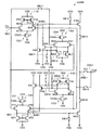
3.1.構成
図3は、基準電圧発生回路20の構成例を示す図である。基準電圧発生回路20は、第1の電圧分割回路(広義には電圧分割回路)80と、第1の電圧分割回路80から供給される電圧のインピーダンス変換を行う複数のインピーダンス変換回路IP1〜IP10(広義には第1〜第Mのインピーダンス変換回路、Mは2以上の整数)と、第2の電圧分割回路90を含む。
3. Reference voltage generation circuit 3.1. Configuration FIG. 3 is a diagram illustrating a configuration example of the reference
インピーダンス変換回路IP1〜IP3(広義には第1〜第P(P<M)のインピーダンス変換回路)及びインピーダンス変換回路IP8〜IP10(広義には第Q(P<Q<M)〜第Mのインピーダンス変換回路)は、その動作範囲が例えば電圧VDD(広義には第1の電源電圧)と電圧VSS(広義には第2の電源電圧)との間の範囲に設定されたRail−to−Rail型であるオペアンプVOPR(広義には第1型の演算増幅器)を含む。 Impedance conversion circuits IP1 to IP3 (first to Pth (P <M) impedance conversion circuits in a broad sense) and impedance conversion circuits IP8 to IP10 (first definition (P <Q <M) to Mth impedance in a broad sense) The operation range of the conversion circuit is, for example, a Rail-to-Rail type whose operating range is set to a range between the voltage VDD (first power supply voltage in a broad sense) and the voltage VSS (second power supply voltage in a broad sense). Are operational amplifiers VOPR (first-type operational amplifiers in a broad sense).
インピーダンス変換回路IP4〜IP7(広義には第P+1〜第P−1のインピーダンス変換回路)は、その動作範囲が電圧VDDよりも低い電圧V3(広義には第3の電圧)と、電圧V3よりも低く電圧VSSよりも高い電圧V4(広義には第4の電圧)との間の範囲に設定された通常型オペアンプVOP(広義には第2型の演算増幅器)を含む。なお、図4に通常型オペアンプVOPの動作範囲を示す。通常型オペアンプVOPでは、図4のR1、R2に示すように入力電圧と出力電圧を等しくすることのできない入力不感帯を有する。これは、入力電圧が供給されるトランジスタの閾値に起因する。即ち、通常型オペアンプVOPの動作範囲は、R3に示すように電圧V3から電圧V4の間である。これに対して、R4に示すように例えば電圧VDD〜電圧VSSの間で動作可能なオペアンプがRail−to−Rail型のオペアンプVOPRである。即ち、通常型オペアンプVOPとRail−to−Rail型オペアンプVOPRとでは、その動作範囲が異なる。オペアンプVOP及びVOPRの構成は後述する。 Impedance conversion circuits IP4 to IP7 (P + 1 to P-1th impedance conversion circuits in a broad sense) have a voltage V3 (third voltage in a broad sense) whose operating range is lower than the voltage VDD and a voltage V3. A normal operational amplifier VOP (second-type operational amplifier in a broad sense) set in a range between a voltage V4 (fourth voltage in a broad sense) that is lower and higher than the voltage VSS is included. FIG. 4 shows the operating range of the normal operational amplifier VOP. The normal type operational amplifier VOP has an input dead zone in which the input voltage and the output voltage cannot be made equal as indicated by R1 and R2 in FIG. This is due to the threshold value of the transistor to which the input voltage is supplied. That is, the operation range of the normal operational amplifier VOP is between the voltage V3 and the voltage V4 as indicated by R3. On the other hand, as shown by R4, an operational amplifier capable of operating between, for example, the voltage VDD and the voltage VSS is a Rail-to-Rail type operational amplifier VOPR. That is, the operational range of the normal operational amplifier VOP and the Rail-to-Rail operational amplifier VOPR are different. The configuration of the operational amplifiers VOP and VOPR will be described later.
第1、第2の電圧分割回路80、90は、例えば複数の抵抗素子が直列接続されるラダー抵抗を含み、ラダー抵抗の各電圧分割端子に基準電圧を発生する。第1の電圧分割回路80は、例えばM種類(図3では例えば10種類)の電圧を出力する。
The first and second
基準電圧発生回路20は、複数の電圧を発生し、例えば階調電圧GV0〜GV63の64種類の電圧を発生するが、これに限定されない。例えば上記のオペアンプVOP1〜VOP8の数を変更したり、第2の電圧分割回路90の抵抗分割数を変更することで、基準電圧発生回路20の発生する電圧の種類を増やしたり減らしたりすることができる。
The reference
第2の電圧分割回路90は、オペアンプVOP1〜VOP8、オペアンプVOPR1〜VOPR4等から供給された電圧をラダー抵抗で抵抗分割することで複数種類の電圧を発生する。第2の電圧分割回路90が出力する複数種類の電圧は例えば基準電圧発生回路20が出力する階調電圧GV1〜GV62に設定される。
The second
なお、オペアンプVOPR5、VOPR6には、それぞれ電圧VDD(例えば電源電圧)、電圧VSS(例えば接地電圧)が供給され、オペアンプVOPR5の出力は例えば基準電圧発生回路20が出力する階調電圧GV0に設定され、オペアンプVOPR6の出力は例えば階調電圧GV63に設定される。 The operational amplifiers VOPR5 and VOPR6 are supplied with a voltage VDD (for example, a power supply voltage) and a voltage VSS (for example, a ground voltage), respectively. The output of the operational amplifier VOPR6 is set to, for example, the gradation voltage GV63.
基準電圧発生回路20は、上記の構成に限定されず、例えば第2の電圧分割回路90を省略するようにしてもよい。また、基準電圧発生回路20のオペアンプVOP及びVOPRの数は一例であって、上記の構成に限定されない。例えば、オペアンプVOPを8個でなく、9個、10個、11個・・・としてもよいし、逆に7個、6個、・・・としてもよい。また、インピーダンス変換回路IP3、IP8のオペアンプVOPR2、VOPR3を省略するようにしても良いし、インピーダンス変換回路IP4〜IP7のオペアンプVOPの後段にRail−to−Rail型のオペアンプVOPRを設けるようにしても良い。
The reference
例えば、インピーダンス変換回路IP2、IP3、IP8、IP9は、通常型オペアンプVOP及びRail−to−Rail型オペアンプVOPRを含む。各インピーダンス変換回路IP2、IP3、IP8、IP9では、この2つのオペアンプVOP、VOPRのオン・オフを例えばレジスタ(広義には初期設定レジスタ)等の設定情報に基づいて排他的に制御する。例えば、インピーダンス変換回路IP2において、オペアンプVOPがオンに設定された場合には、オペアンプVOPRがオフに設定される。なお、使用されないオペアンプVOP、VOPRはオフに設定されるため、無駄な電力消費を抑制できる。 For example, the impedance conversion circuits IP2, IP3, IP8, and IP9 include a normal type operational amplifier VOP and a Rail-to-Rail type operational amplifier VOPR. Each of the impedance conversion circuits IP2, IP3, IP8, and IP9 exclusively controls on / off of the two operational amplifiers VOP and VOPR based on setting information such as a register (initial setting register in a broad sense). For example, in the impedance conversion circuit IP2, when the operational amplifier VOP is set to ON, the operational amplifier VOPR is set to OFF. In addition, since the operational amplifiers VOP and VOPR that are not used are set off, useless power consumption can be suppressed.
このように、フレキシブルに各インピーダンス変換回路IP2、IP3、IP8、IP9の各オペアンプVOP、VOPRのオン・オフを制御することができる。これにより、基準電圧発生回路20は、さまざまなパネルの表示特性(例えばγ(ガンマ)特性)に対して、柔軟に対応することができる。また、ユーザーは初期設定レジスタを適宜に設定することで、適用したいパネルの表示特性に最適な設定を保存できる。これにより、基準電圧発生回路20は常にパネルに対して最適な階調電圧GV0〜GV63を低消費電力で供給することができる。
In this way, the operational amplifiers VOP and VOPR of the impedance conversion circuits IP2, IP3, IP8, and IP9 can be flexibly controlled. Thereby, the reference
また、図5に示すように、第2の電圧分割回路90を省略し、各階調電圧GV0〜GV63の出力にオペアンプを用いるような構成でも良い。図5の基準電圧発生回路21は、例えば64階調表示に対応するためにインピーダンス変換回路IP1’〜IP64’を含む。各インピーダンス変換回路IP1’〜IP64’の出力が階調電圧GV0〜GV63に設定される。また、第1の電圧分割回路80は64種類の電圧V0’〜V63’を出力する。
Further, as shown in FIG. 5, the second
インピーダンス変換回路IP1’〜IP3’、IP62’〜IP64’にはRail−to−Rail型オペアンプVOPRが設けられ、インピーダンス変換回路IP2’〜IP63’には通常型オペアンプVOPが設けられている。この場合も同様に、インピーダンス変換回路IP2’、IP3’、IP62’、IP63’では、設定情報に基づいてRail−to−Rail型オペアンプVOPR及び通常型オペアンプVOPのオン・オフを排他的に制御する。 The impedance conversion circuits IP1 'to IP3' and IP62 'to IP64' are provided with rail-to-rail type operational amplifiers VOPR, and the impedance conversion circuits IP2 'to IP63' are provided with normal type operational amplifiers VOP. Similarly, in this case, the impedance conversion circuits IP2 ′, IP3 ′, IP62 ′, and IP63 ′ exclusively control on / off of the rail-to-rail type operational amplifier VOPR and the normal type operational amplifier VOP based on the setting information. .
図6は、図3の基準電圧発生回路20の第1、第2の電圧分割回路80、90の詳細を示す。電圧発生回路95は振幅調整レジスタ24の設定情報に基づいて、第1の電圧分割回路80に供給する電圧を生成する。ここでは、第1の電圧分割回路80には例えば電圧VDD及び電圧VSSが供給されることとする。
FIG. 6 shows details of the first and second
第1の電圧分割回路80は、複数の可変抵抗VRと、複数のラダー抵抗DRを含む。傾き調整レジスタ26によって、階調電圧GV0〜GV63の変化の傾きを調整することができる。傾き調整レジスタ26には、可変抵抗VRの抵抗値を設定する情報が格納されている。各可変抵抗VRは、傾き調整レジスタ26の設定情報に基づいて、その抵抗値が設定される。なお、図6に記載されている“16to1”は、例えば16種類に抵抗値が可変である場合の、そのうちの1種類に選択することを意味する。
The first
微調整レジスタ28は、階調電圧GV0〜GV63の電圧レベルの微調整を行うための設定情報が格納されている。セレクタSLは、ラダー抵抗DRから抵抗分割によって電圧分割された複数種類の電圧のうち、微調整レジスタの設定情報に基づいて、その複数種類の電圧から一つの電圧を選択する。図6に記載されている“8to1”は、例えば8種類に電圧分割された電圧値のうちの1種類を選択することを意味する。 The fine adjustment register 28 stores setting information for fine adjustment of the voltage levels of the gradation voltages GV0 to GV63. The selector SL selects one voltage from the plurality of types of voltages based on the setting information of the fine adjustment register among the plurality of types of voltages divided from the ladder resistor DR by resistance division. “8to1” described in FIG. 6 means that, for example, one type of voltage values divided into eight types is selected.
なお、各レジスタ24、26、28は、ユーザーが適宜に設定可能な情報が格納される。
The
また、第2の電圧分割回路90は、複数の抵抗が直列に接続されたラダー抵抗を含む。階調電圧GV1〜GV62は、第2の電圧分割回路90によって電圧分割された電圧に基づく。ここで、例えば階調電圧GV2〜GV61に対応して“2to1”と記載されているのは、基準電圧VCOMの正極時と負極時とで階調電圧GV2〜GV61の電圧値を変更するためである。例えば階調電圧GV2として用意された2種類の電圧値のうち、基準電圧VCOMが正極である場合には一方の電圧を選択し、基準電圧VCOMが負極である場合には他方の電圧を選択する。
The second
これは、一般的に、VCOMの正極期間と負極期間とでは縺iガンマ)補正特性(階調特性)が非対称になるためである。つまり、このように縺iガンマ)補正特性が非対称になる場合にも、図6のようにラダー抵抗の抵抗分割を正極性用、負極性用とで変更することで、VCOMの正極期間、負極期間の各期間に最適な縺iガンマ)補正を行うことが可能になる。なお、第1の電圧分割回路80においても、基準電圧VCOMの正極・負極に基づいて、微調整レジスタ28を設定することで、各インピーダンス変換回路IP3〜IP8に入力される電圧を変更可能である。
This is because the correction characteristic (gradation characteristic) is generally asymmetric between the positive and negative periods of VCOM. That is, even when the correction characteristic is asymmetrical as described above, the resistance division of the ladder resistor is changed between positive polarity and negative polarity as shown in FIG. It becomes possible to perform an optimal (i-gamma) correction for each period. In the first
3.2.通常型オペアンプVOP
図7に通常型オペアンプVOPの回路例を示す。図7のオペアンプVOPは、p型トランジスタM7、M8、n型トランジスタM5、M6、及びトランジスタCSb(広義にはバイアス電流用トランジスタ)を含むp型差動入力回路によりn型駆動トランジスタM10を制御する。またp型トランジスタM1、M2、n型トランジスタM3、M4、及びトランジスタCSa(広義にはバイアス電流用トランジスタ)を含むn型差動入力回路によりp型駆動トランジスタM9を制御する。
3.2. Normal type operational amplifier VOP
FIG. 7 shows a circuit example of the normal operational amplifier VOP. The operational amplifier VOP in FIG. 7 controls the n-type drive transistor M10 by a p-type differential input circuit including p-type transistors M7 and M8, n-type transistors M5 and M6, and a transistor CSb (bias current transistor in a broad sense). . The p-type driving transistor M9 is controlled by an n-type differential input circuit including p-type transistors M1 and M2, n-type transistors M3 and M4, and a transistor CSa (bias current transistor in a broad sense).
n型差動入力回路に着目して、入力信号Vinの電圧が出力信号Voutの電圧より大きい場合を考える。この場合、n型トランジスタM4のインピーダンスがn型トランジスタM3より大きくなるため、p型トランジスタM2、M1のゲート電圧が上昇し、p型トランジスタM1のインピーダンスが大きくなる。そのため、p型駆動トランジスタM9のゲート電圧が下降し、p型駆動トランジスタM9はオンする方向に向かう。 Focusing on the n-type differential input circuit, consider a case where the voltage of the input signal Vin is larger than the voltage of the output signal Vout. In this case, since the impedance of the n-type transistor M4 is larger than that of the n-type transistor M3, the gate voltages of the p-type transistors M2 and M1 are increased, and the impedance of the p-type transistor M1 is increased. Therefore, the gate voltage of the p-type drive transistor M9 decreases, and the p-type drive transistor M9 is turned on.
p型差動入力回路に着目すると、入力信号Vinの電圧が出力信号Voutの電圧より大きい場合、p型トランジスタM8のインピーダンスがp型トランジスタM7のインピーダンスより小さくなるため、n型トランジスタM5、M6のゲート電圧が上昇し、n型トランジスタM5のインピーダンスが小さくなる。そのため、n型駆動トランジスタM10のゲート電圧が下降し、n型駆動トランジスタM10がオフする方向に向かう。 Focusing on the p-type differential input circuit, when the voltage of the input signal Vin is larger than the voltage of the output signal Vout, the impedance of the p-type transistor M8 is smaller than the impedance of the p-type transistor M7. The gate voltage increases and the impedance of the n-type transistor M5 decreases. For this reason, the gate voltage of the n-type drive transistor M10 decreases and the n-type drive transistor M10 is turned off.
このように、入力信号Vinの電圧が出力信号Voutの電圧より大きい場合は、出力信号Voutの電圧が大きくなる方向にp型駆動トランジスタM9、n型駆動トランジスタM10が動作する。なお、入力信号Vinの電圧が出力信号Voutの電圧より小さい場合は、上述と逆の動作を行う。以上のような動作の結果、演算増幅器では、入力信号Vinの電圧と出力信号Voutの電圧とがほぼ等しくなる平衡状態に移行していく。 Thus, when the voltage of the input signal Vin is larger than the voltage of the output signal Vout, the p-type drive transistor M9 and the n-type drive transistor M10 operate in the direction in which the voltage of the output signal Vout increases. If the voltage of the input signal Vin is smaller than the voltage of the output signal Vout, the operation opposite to that described above is performed. As a result of the above operation, the operational amplifier shifts to an equilibrium state in which the voltage of the input signal Vin and the voltage of the output signal Vout are substantially equal.
しかしながら、p型差動入力回路では入力信号Vinがゲート電圧としてp型トランジスタM7に供給され、n型差動入力回路では入力信号Vinがゲート電圧としてn型トランジスタM3に供給される。そのため、図4に示すように、入力信号Vinが、高電位側の電源電圧VDD〜VDD−|Vthp|(Vthpは、p型トランジスタM7の閾値電圧)の範囲R1と、低電位側の電源電圧VSS〜VSS+Vthn(Vthnは、n型トランジスタM3の閾値電圧)の範囲R2では、入力信号Vinの電圧と出力信号Voutの電圧とを等しくできない入力不感帯となる。これは、低電位側の電源電圧VSS〜VSS+Vthnの範囲R2では、n型トランジスタM3がオフ状態のままであるためn型差動入力回路が動作せず、高電位側の電源電圧VDD〜VDD−|Vthp|の範囲R1では、p型トランジスタM7がオフ状態のままであるためp型差動入力回路が動作しないからである。 However, in the p-type differential input circuit, the input signal Vin is supplied as a gate voltage to the p-type transistor M7, and in the n-type differential input circuit, the input signal Vin is supplied as a gate voltage to the n-type transistor M3. Therefore, as shown in FIG. 4, the input signal Vin has a range R1 in which the high-potential side power supply voltage VDD to VDD− | Vthp | (Vthp is the threshold voltage of the p-type transistor M7) and the low-potential side power supply voltage. In the range R2 of VSS to VSS + Vthn (Vthn is a threshold voltage of the n-type transistor M3), an input dead zone is obtained in which the voltage of the input signal Vin and the voltage of the output signal Vout cannot be equal. This is because the n-type differential input circuit does not operate in the range R2 of the low-potential-side power supply voltage VSS to VSS + Vthn, so the n-type differential input circuit does not operate, and the high-potential-side power supply voltage VDD to VDD− This is because, in the range R1 of | Vthp |, the p-type differential input circuit does not operate because the p-type transistor M7 remains off.
なお、トランジスタCSa、CSbの各ゲートに入力されるゲート電圧CSaG、CSbGを調整することで、n型差動入力回路及びp型差動入力回路の電流源を調整することができる。 Note that the current sources of the n-type differential input circuit and the p-type differential input circuit can be adjusted by adjusting the gate voltages CSaG and CSbG input to the gates of the transistors CSa and CSb.
また、通常型オペアンプVOPは、スイッチSW21(広義には第1のスイッチ)、スイッチSW22(広義には第2のスイッチ)、スイッチSW23(広義には第3のスイッチ)、スイッチSW24(広義には第4のスイッチ)、スイッチSW25(広義には第5のスイッチ)、スイッチSW26(広義には第6のスイッチ)及び出力イネーブルスイッチOE2(広義には出力イネーブルスイッチ)を含む。 The normal operational amplifier VOP includes a switch SW21 (first switch in a broad sense), a switch SW22 (second switch in a broad sense), a switch SW23 (third switch in a broad sense), and a switch SW24 (in a broad sense). A fourth switch), a switch SW25 (fifth switch in a broad sense), a switch SW26 (sixth switch in a broad sense), and an output enable switch OE2 (an output enable switch in a broad sense).
スイッチSW21は、入力信号Vinが入力される入力ノードIND2と出力信号Voutが出力される出力ノードOND2(広義には出力部)との間に設けられている。スイッチSW22は、電圧VSSを発生する電源(広義には第2の電源)と出力ノードND21との間に設けられている。スイッチSW23は、電圧VDDを発生する電源(広義には第1の電源)と出力ノードND22との間に設けられている。スイッチSW24は、出力ノードOND2とトランジスタM4のゲートとの間に設けられている。スイッチSW25は、電圧VDDを発生する電源と中間ノードMND2との間に設けられている。スイッチSW26は、電圧VSSを発生する電源と中間ノードMND2との間に設けられている。出力イネーブルスイッチOE2は中間ノードMND2と出力ノードOND2との間に設けられている。 The switch SW21 is provided between an input node IND2 to which the input signal Vin is input and an output node OND2 (output unit in a broad sense) from which the output signal Vout is output. The switch SW22 is provided between a power source (second power source in a broad sense) that generates the voltage VSS and the output node ND21. The switch SW23 is provided between the power supply (first power supply in a broad sense) that generates the voltage VDD and the output node ND22. The switch SW24 is provided between the output node OND2 and the gate of the transistor M4. The switch SW25 is provided between the power supply that generates the voltage VDD and the intermediate node MND2. The switch SW26 is provided between the power supply that generates the voltage VSS and the intermediate node MND2. The output enable switch OE2 is provided between the intermediate node MND2 and the output node OND2.
例えば図3のインピーダンス変換回路IP2、IP3、IP8、IP9等のいずれかにおいて、通常型オペアンプVOPがオンに設定された場合には、スイッチSW21、スイッチSW24、スイッチSW25、スイッチSW26、出力イネーブルスイッチOE2がオンに設定される。また、スイッチSW22、SW23はオフに設定される。即ち、図7に示すような状態になる。 For example, in any of the impedance conversion circuits IP2, IP3, IP8, IP9, etc. in FIG. 3, when the normal operational amplifier VOP is set to ON, the switch SW21, the switch SW24, the switch SW25, the switch SW26, and the output enable switch OE2 Is set to on. Also, the switches SW22 and SW23 are set to off. That is, the state shown in FIG. 7 is obtained.
一方、インピーダンス変換回路IP2等において、Rail−to−Rail型オペアンプVOPRがオンに設定され、通常型オペアンプVOPがオフに設定された場合には、スイッチSW21、スイッチSW24、スイッチSW25、スイッチSW26、出力イネーブルスイッチOE2がオフに設定される。また、スイッチSW22、SW23はオンに設定される。即ち、図8に示すような状態になる。これにより、トランジスタM9、M10は確実にオフにされ、出力ノードOND2はハイインピーダンス状態に設定される。さらに、トランジスタCSa、CSbのゲートに入力されるゲート電圧CSaG、CSbGを制御する(例えばトランジスタCSa、CSbをオフにする)ことで、n型差動入力回路及びp型差動入力回路の電流源の電流供給をオフにすることができる。これにより、通常型オペアンプVOPがオフに設定されている場合に、通常型オペアンプVOPによる無駄な電力消費を抑制できる。 On the other hand, in the impedance conversion circuit IP2 or the like, when the Rail-to-Rail type operational amplifier VOPR is set to ON and the normal type operational amplifier VOP is set to OFF, the switch SW21, the switch SW24, the switch SW25, the switch SW26, the output The enable switch OE2 is set off. Also, the switches SW22 and SW23 are set on. That is, the state shown in FIG. Thereby, the transistors M9 and M10 are reliably turned off, and the output node OND2 is set to a high impedance state. Further, by controlling gate voltages CSaG and CSbG inputted to the gates of the transistors CSa and CSb (for example, turning off the transistors CSa and CSb), current sources of the n-type differential input circuit and the p-type differential input circuit Current supply can be turned off. Thereby, when the normal type operational amplifier VOP is set to OFF, wasteful power consumption by the normal type operational amplifier VOP can be suppressed.
3.3.Rail−to−Rail型オペアンプVOPR
図9に本実施形態に係るRail−to−Rail型オペアンプVOPRの構成例を示す。
3.3. Rail-to-Rail type operational amplifier VOPR
FIG. 9 shows a configuration example of a Rail-to-Rail type operational amplifier VOPR according to this embodiment.
このオペアンプVOPRは、p型(例えば第1の導電型)差動増幅回路100と、n型(例えば第2の導電型)差動増幅回路110と、出力回路120とを含む。p型差動増幅回路100、n型差動増幅回路110、及び出力回路120は、高電位側の電源電圧VDD(広義には第1の電源電圧)と低電位側の電源電圧VSS(広義には第2の電源電圧)との間の電圧を動作電圧とする。
The operational amplifier VOPR includes a p-type (for example, first conductivity type)
p型差動増幅回路100は、入力信号Vin及び出力信号Voutの差分を増幅する。p型差動増幅回路100は、出力ノードND1(第1の出力ノード)及び反転出力ノードNXD1(第1の反転出力ノード)を有し、出力ノードND1及び反転出力ノードNXD1の間に入力信号Vin及び出力信号Voutの差分に対応した電圧を出力する。
The p-type
このp型差動増幅回路100は、第1のカレントミラー回路CM1と、p型(第1の導電型)の第1の差動トランジスタ対を有する。第1の差動トランジスタ対は、p型金属酸化膜半導体(Metal Oxide Semiconductor:以下MOSと略す)トランジスタ(以下、M
OSトランジスタを単にトランジスタと略す)PT1、PT2を含む。p型トランジスタPT1、PT2の各トランジスタのソースが第1の電流源CS1に接続されると共に、入力信号Vin及び出力信号Voutが各トランジスタのゲートに入力される。p型トランジスタPT1、PT2のドレイン電流は、第1のカレントミラー回路CM1によって生成される。p型トランジスタPT1のゲートに入力信号Vinが入力される。p型トランジスタPT2のゲートに出力信号Voutが入力される。p型トランジスタPT1のドレインが、出力ノードND1(第1の出力ノード)になる。p型トランジスタPT2のドレインが、反転出力ノードNXD1(第1の反転出力ノード)になる。
The p-type
OS transistors are simply abbreviated as transistors) and include PT1 and PT2. The sources of the p-type transistors PT1 and PT2 are connected to the first current source CS1, and the input signal Vin and the output signal Vout are input to the gates of the transistors. The drain currents of the p-type transistors PT1 and PT2 are generated by the first current mirror circuit CM1. An input signal Vin is input to the gate of the p-type transistor PT1. The output signal Vout is input to the gate of the p-type transistor PT2. The drain of the p-type transistor PT1 becomes the output node ND1 (first output node). The drain of the p-type transistor PT2 becomes the inverted output node NXD1 (first inverted output node).
n型差動増幅回路110は、入力信号Vin及び出力信号Voutの差分を増幅する。n型差動増幅回路110は、出力ノードND2(第2の出力ノード)及び反転出力ノードNXD2(第2の反転出力ノード)を有し、出力ノードND2及び反転出力ノードNXD2の間に入力信号Vin及び出力信号Voutの差分に対応した電圧を出力する。
The n-type
このn型差動増幅回路110は、第2のカレントミラー回路CM2と、n型(第2の導電型)の第2の差動トランジスタ対を含む。第2の差動トランジスタ対は、n型トランジスタNT3、NT4を含む。n型トランジスタNT3、NT4の各トランジスタのソースが第2の電流源CS2に接続されると共に、入力信号Vin及び出力信号Voutが各トランジスタのゲートに入力される。n型トランジスタNT3、NT4のドレイン電流は、第2のカレントミラー回路CM2によって生成される。n型トランジスタNT3のゲートに入力信号Vinが入力される。n型トランジスタNT4のゲートに出力信号Voutが入力される。n型トランジスタNT3のドレインが、出力ノードND2(第2の出力ノード)になる。n型トランジスタNT4のドレインが、反転出力ノードNXD2(第2の反転出力ノード)になる。
The n-type
出力回路120は、p型差動増幅回路100の出力ノードND1(第1の出力ノード)の電圧とn型差動増幅回路110の出力ノードND2(第2の出力ノード)の電圧とに基づいて、出力信号Voutを生成する。
The
この出力回路120は、n型(第2の導電型)の第1の駆動トランジスタNTO1とp型(第1の導電型)の第2の駆動トランジスタPTO1とを含む。第1の駆動トランジスタNTO1のゲート(電圧)は、p型差動増幅回路100の出力ノードND1(第1の出力ノード)の電圧に基づいて制御される。第2の駆動トランジスタPTO1のゲート(電圧)は、n型差動増幅回路110の出力ノード(ND2)(第2の出力ノード)の電圧に基づいて制御される。第2の駆動トランジスタPTO1のドレインは、第1の駆動トランジスタNTO1のドレインに接続される。そして出力回路120は、第1の駆動トランジスタNTO1のドレインの電圧(第2の駆動トランジスタPTO1のドレインの電圧)を、出力信号Voutとして出力する。
The
更に本実施形態における演算増幅器は、第1及び第2の補助回路130、140を含むことで、入力不感帯をなくし、かつ貫通電流を抑える。この結果、動作電圧の範囲を不要に広げることなく、貫通電流を抑えて低消費電力化を実現する。
Furthermore, the operational amplifier according to the present embodiment includes the first and second
ここで、第1の補助回路130は、入力信号Vin及び出力信号Voutに基づいて、p型差動増幅回路100の出力ノードND1(第1の出力ノード)及び反転出力ノードNXD1(第1の反転出力ノード)のうち少なくとも一方を駆動する。また第2の補助回路130は、入力信号Vin及び出力信号Voutに基づいて、n型差動増幅回路110の出力ノードND2(第2の出力ノード)及び第2の反転出力ノード(NXD2)のうち少なくとも一方を駆動する。
Here, the first
そして、p型トランジスタPT1(第1の差動トランジスタ対を構成するトランジスタのうち入力信号Vinがゲートに入力されるトランジスタ)のゲート・ソース間(ゲートとソースとの間)の電圧の絶対値がp型トランジスタPT1の閾値電圧の絶対値より小さいとき、第1の補助回路130が、出力ノードND1(第1の出力ノード)及び反転出力ノードNXD1(第1の反転出力ノード)の少なくとも一方を駆動することで、第1の駆動トランジスタNTO1のゲート電圧を制御する。
The absolute value of the voltage between the gate and the source (between the gate and the source) of the p-type transistor PT1 (the transistor in which the input signal Vin is input to the gate among the transistors constituting the first differential transistor pair) is When smaller than the absolute value of the threshold voltage of the p-type transistor PT1, the first
更に、n型トランジスタNT3(第2の差動トランジスタ対を構成するトランジスタのうち入力信号Vinがゲートに入力されるトランジスタ)のゲート・ソース間の電圧の絶対値がn型トランジスタNT3の閾値電圧の絶対値より小さいとき、第2の補助回路140が、出力ノードND2(第2の出力ノード)及び反転出力ノードNXD2(第2の反転出力ノード)の少なくとも一方を駆動することで、第2の駆動トランジスタPTO1のゲート電圧を制御する。
Furthermore, the absolute value of the voltage between the gate and the source of the n-type transistor NT3 (the transistor in which the input signal Vin is input to the gate among the transistors constituting the second differential transistor pair) is the threshold voltage of the n-type transistor NT3. When smaller than the absolute value, the second
図10に、図5に示すオペアンプVOPRの動作説明図を示す。 FIG. 10 is an operation explanatory diagram of the operational amplifier VOPR shown in FIG.
ここで、高電位側の電源電圧をVDD、低電位側の電源電圧をVSS、入力信号の電圧をVin、p型トランジスタPT1の閾値電圧をVthp、n型トランジスタNT3の閾値電圧Vthnとする。 Here, the power supply voltage on the high potential side is VDD, the power supply voltage on the low potential side is VSS, the voltage of the input signal is Vin, the threshold voltage of the p-type transistor PT1 is Vthp, and the threshold voltage Vthn of the n-type transistor NT3.
VDD≧Vin>VDD−|Vthp|では、p型トランジスタがオフ、n型トランジスタがオンとなる。ここでp型トランジスタがゲート電圧に応じてカットオフ領域、線形領域、又は飽和領域で動作する場合、p型トランジスタがオフとは、カットオフ領域であることを意味する。同様にn型トランジスタがゲート電圧に応じてカットオフ領域、線形領域、又は飽和領域で動作する場合、n型トランジスタがオンとは、線形領域又は飽和領域であることを意味する。従って、VDD≧Vin>VDD−|Vthp|では、p型差動増幅回路100は動作せず(オフ)、n型差動増幅回路110は動作する(オン)。そこで第1の補助回路130の動作をオン(出力ノードND1(第1の出力ノード)及び反転出力ノードNXD1(第1の反転出力ノード)の少なくとも一方を駆動させ)し、第2の補助回路140の動作をオフ(出力ノードND2(第2の出力ノード)及び反転出力ノードNXD1(第2の反転出力ノード)を駆動させない)する。このように、p型差動増幅回路100が動作しない範囲で、第1の補助回路130によりp型差動増幅回路100の出力ノードND1(反転出力ノードNXD1)を駆動することで、p型差動増幅回路100の第1の差動トランジスタ対の入力不感帯の範囲の入力信号Vinに対しても、出力ノードND1の電圧を不定状態にすることがなくなる。
When VDD ≧ Vin> VDD− | Vthp |, the p-type transistor is turned off and the n-type transistor is turned on. Here, when the p-type transistor operates in a cut-off region, a linear region, or a saturation region in accordance with the gate voltage, the p-type transistor is off means that it is a cut-off region. Similarly, when an n-type transistor operates in a cut-off region, a linear region, or a saturation region depending on a gate voltage, the n-type transistor is on means that it is a linear region or a saturation region. Therefore, when VDD ≧ Vin> VDD− | Vthp |, the p-type
VDD−|Vthp|≧Vin≧Vthn+VSSでは、p型トランジスタがオン、n型トランジスタがオンとなる。ここでp型トランジスタがゲート電圧に応じてカットオフ領域、線形領域、又は飽和領域で動作する場合、p型トランジスタがオンとは、線形領域又は飽和領域であることを意味する。従って、p型差動増幅回路100は動作し(オン)、n型差動増幅回路110も動作する(オン)。この場合、第1の補助回路130の動作をオン又はオフし、第2の補助回路140の動作をオン又はオフする。即ち、p型差動増幅回路100及びn型差動増幅回路110が動作するため、出力ノードND1、ND2が不定状態にならず、図13に示す構成の差動増幅器と同様に、出力回路120により出力信号Voutを出力する。従って、第1及び第2補助回路130、140を動作させてもよいし、動作させなくてもよい。図5では、動作をオンさせている。
When VDD− | Vthp | ≧ Vin ≧ Vthn + VSS, the p-type transistor is turned on and the n-type transistor is turned on. Here, when the p-type transistor operates in the cut-off region, the linear region, or the saturation region according to the gate voltage, the p-type transistor is on means that the p-type transistor is in the linear region or the saturation region. Therefore, the p-type
Vthn+VSS>Vin≧VSSでは、p型トランジスタがオン、n型トランジスタがオフとなる。ここでn型トランジスタがゲート電圧に応じてカットオフ領域、線形領域、又は飽和領域で動作する場合、n型トランジスタがオフとは、カットオフ領域であることを意味する。従って、n型差動増幅回路110は動作せず(オフ)、p型差動増幅回路100は動作する(オン)。そこで第2の補助回路140の動作をオン(出力ノードND2(第2の出力ノード)及び反転出力ノードNXD2(第2の反転出力ノード)の少なくとも一方を駆動させ)し、第1の補助回路130の動作をオフする。このように、n型差動増幅回路110が動作しない範囲で、第2の補助回路140によりn型差動増幅回路110の出力ノードND2(反転出力ノードNXD2)を駆動することで、n型差動増幅回路110の第2の差動トランジスタ対の入力不感帯の範囲の入力信号Vinに対しても、出力ノードND2の電圧を不定状態にすることがなくなる。
When Vthn + VSS> Vin ≧ VSS, the p-type transistor is turned on and the n-type transistor is turned off. Here, when the n-type transistor operates in a cut-off region, a linear region, or a saturation region depending on the gate voltage, the n-type transistor is off means that it is a cut-off region. Therefore, the n-type
以上のように第1及び第2の補助回路130、140により、出力回路120を構成する第1及び第2の駆動トランジスタNTO1、PTO1のゲート電圧が制御できるようになり、入力信号Vinが入力不感帯の範囲であることに起因する不要な貫通電流の発生を無くすことができる。しかも、入力信号Vinの入力不感帯を無くすことで、p型トランジスタの閾値電圧Vthp及びn型トランジスタの閾値電圧Vthnのばらつきを考慮して約1.9ボルトのオフセットを設ける必要がなくなる。そのため、高電位側の電源電圧VDDと低電位側の電源電圧VSSとの間の電圧を振幅として、演算増幅器を形成できるようになるので、駆動能力を低下させることなく動作電圧を狭くでき、更に消費電力を削減できるようになる。これは、昇圧回路の実装や製造プロセスの低耐圧化を意味し、低コスト化を実現する。
As described above, the gate voltages of the first and second drive transistors NTO1 and PTO1 constituting the
以下では、本実施形態におけるオペアンプVOPRの詳細な構成例について説明する。 Below, the detailed structural example of operational amplifier VOPR in this embodiment is demonstrated.
図9において、p型差動増幅回路100は、第1の電流源CS1と、上述の第1の差動トランジスタ対と、第1のカレントミラー回路CM1とを含む。第1の電流源CS1の一端に、高電位側の電源電圧VDD(第1の電源電圧)が供給される。第1の電流源CS1の他端に、上述の第1の差動トランジスタ対を構成するp型トランジスタPT1、PT2のソースが接続される。
In FIG. 9, the p-type
第1のカレントミラー回路CM1は、ゲート同士が互いに接続されたn型(第2の導電型)の第1のトランジスタ対を含む。この第1のトランジスタ対は、n型トランジスタNT1、NT2を含む。n型トランジスタNT1、NT2の各トランジスタのソースに低電位側の電源電圧VSS(第2の電源電圧)が供給される。n型トランジスタNT1のドレインが出力ノードND1(第1の出力ノード)に接続される。n型トランジスタNT2のドレインが反転出力ノードNXD1(第1の反転出力ノード)に接続される。n型トランジスタNT2(第1の差動トランジスタ対を構成するトランジスタのうち反転出力ノードNXD1に接続されるトランジスタ)のドレイン及びゲートが接続される。 The first current mirror circuit CM1 includes an n-type (second conductivity type) first transistor pair whose gates are connected to each other. The first transistor pair includes n-type transistors NT1 and NT2. The low-potential-side power supply voltage VSS (second power supply voltage) is supplied to the sources of the n-type transistors NT1 and NT2. The drain of n-type transistor NT1 is connected to output node ND1 (first output node). The drain of the n-type transistor NT2 is connected to the inverting output node NXD1 (first inverting output node). The drain and gate of an n-type transistor NT2 (a transistor connected to the inverting output node NXD1 among the transistors constituting the first differential transistor pair) are connected.
またn型差動増幅回路110は、第2の電流源CS2と、上述の第2の差動トランジスタ対と、第2のカレントミラー回路CM2とを含む。第2の電流源CS2の一端に、低電位側の電源電圧VSS(第2の電源電圧)が供給される。第2の電流源CS2の他端に、上述の第2の差動トランジスタ対を構成するn型トランジスタNT3、NT4のソースが接続される。
The n-type
第2のカレントミラー回路CM2は、ゲート同士が互いに接続されたp型(第1の導電型)の第2のトランジスタ対を含む。この第2のトランジスタ対は、p型トランジスタPT3、PT4を含む。p型トランジスタPT3、PT4の各トランジスタのソースに高電位側の電源電圧VDD(第1の電源電圧)が供給される。p型トランジスタPT3のドレインが出力ノードND2(第2の出力ノード)に接続される。p型トランジスタPT4のドレインが反転出力ノードNXD2(第2の反転出力ノード)に接続される。p型トランジスタPT4(第2のトランジスタ対を構成するトランジスタのうち反転出力ノードNXD2に接続されるトランジスタ)のドレイン及びゲートが接続される。 The second current mirror circuit CM2 includes a p-type (first conductivity type) second transistor pair whose gates are connected to each other. This second transistor pair includes p-type transistors PT3 and PT4. The power supply voltage VDD (first power supply voltage) on the high potential side is supplied to the sources of the p-type transistors PT3 and PT4. The drain of the p-type transistor PT3 is connected to the output node ND2 (second output node). The drain of the p-type transistor PT4 is connected to the inverting output node NXD2 (second inverting output node). The drain and gate of a p-type transistor PT4 (a transistor connected to the inverting output node NXD2 among the transistors constituting the second transistor pair) are connected.
また第1の補助回路130は、p型(第1の導電型)の第1及び第2の電流駆動トランジスタPA1、PA2と、第1の電流制御回路132とを含むことができる。第1及び第2の電流駆動トランジスタPA1、PA2の各トランジスタのソースに、高電位側の電源電圧VDD(第1の電源電圧)が供給される。第1の電流駆動トランジスタPA1のドレインは、出力ノードND1(第1の出力ノード)に接続される。第2の電流駆動トランジスタPA2のドレインは、反転出力ノードNXD1(第1の反転出力ノード)に接続される。
The first
そして、第1の電流制御回路132が、入力信号Vin及び出力信号Voutに基づいて第1及び第2の電流駆動トランジスタPA1、PA2のゲート電圧を制御する。より具体的には、第1の差動トランジスタ対を構成するトランジスタのうち入力信号Vinがゲートに入力されるp型トランジスタPT1のゲート・ソース間の電圧(の絶対値)が該トランジスタの閾値電圧(の絶対値)より小さいとき、第1の電流制御回路132が、出力ノードND1(第1の出力ノード)及び反転出力ノードNXD1(第1の反転出力ノード)の少なくとも一方を駆動するように第1及び第2の電流駆動トランジスタPA1、PA2のゲート電圧を制御する。
Then, the first
また第2の補助回路140は、n型(第2の導電型)の第3及び第4の電流駆動トランジスタNA3、NA4と、第2の電流制御回路142とを含むことができる。第3及び第4の電流駆動トランジスタNA3、NA4の各トランジスタのソースに、低電位側の電源電圧VSS(第2の電源電圧)が供給される。第3の電流駆動トランジスタNA3のドレインは、出力ノードND2(第2の出力ノード)に接続される。第4の電流駆動トランジスタNA4のドレインは、反転出力ノードNXD2(第2の反転出力ノード)に接続される。
The second
そして、第2の電流制御回路142が、入力信号Vin及び出力信号Voutに基づいて第3及び第4の電流駆動トランジスタNA3、NA4のゲート電圧を制御する。より具体的には、第2の差動トランジスタ対を構成するトランジスタのうち入力信号Vinがゲートに入力されるn型トランジスタNT3のゲート・ソース間の電圧の絶対値が該トランジスタの閾値電圧の絶対値より小さいとき、第2の電流制御回路142が、出力ノードND2(第2の出力ノード)及び反転出力ノードNXD2(第2の反転出力ノード)の少なくとも一方を駆動するように第3及び第4の電流駆動トランジスタNA3、NA4のゲート電圧を制御する。
Then, the second
図11に、第1の電流制御回路132の構成例を示す。
FIG. 11 shows a configuration example of the first
第1の電流制御回路132は、第3の電流源CS3と、n型(第2の導電型)の第3の差動トランジスタ対と、p型(第1の導電型)の第5及び第6の電流駆動トランジスタPS5、PS6とを含む。
The first
第3の電流源CS3の一端に、低電位側の電源電圧VSS(第2の電源電圧)が供給される。 A low-potential-side power supply voltage VSS (second power supply voltage) is supplied to one end of the third current source CS3.
第3の差動トランジスタ対は、n型トランジスタNS5、NS6を含む。n型トランジスタNS5、NS6の各トランジスタのソースが、第3の電流源CS3の他端に接続される。n型トランジスタNS5のゲートに、入力信号Vinが入力される。n型トランジスタNS6のゲートに、出力信号Voutが入力される。 The third differential transistor pair includes n-type transistors NS5 and NS6. The sources of the n-type transistors NS5 and NS6 are connected to the other end of the third current source CS3. The input signal Vin is input to the gate of the n-type transistor NS5. The output signal Vout is input to the gate of the n-type transistor NS6.
第5及び第6の電流駆動トランジスタPS5、PS6の各トランジスタのソースに、高電位側の電源電圧VDD(第1の電源電圧)が供給される。第5の電流駆動トランジスタPS5のドレインが、第3の差動トランジスタ対を構成するn型トランジスタNS5のドレインに接続される。第6の電流駆動トランジスタPS6のドレインが、第3の差動トランジスタ対を構成するn型トランジスタNS6のドレインに接続される。第5の電流駆動トランジスタPS5のゲート及びドレインが接続される。第6の電流駆動トランジスタPS6のゲート及びドレインが接続される。 The high-potential-side power supply voltage VDD (first power supply voltage) is supplied to the sources of the fifth and sixth current drive transistors PS5 and PS6. The drain of the fifth current driver transistor PS5 is connected to the drain of the n-type transistor NS5 constituting the third differential transistor pair. The drain of the sixth current driver transistor PS6 is connected to the drain of the n-type transistor NS6 constituting the third differential transistor pair. The gate and drain of the fifth current driver transistor PS5 are connected. The gate and drain of the sixth current driver transistor PS6 are connected.
そして、第3の差動トランジスタ対を構成するn型トランジスタNS5(第3の差動トランジスタ対を構成するトランジスタのうちそのゲートに入力信号Vinが入力されるトランジスタ)のドレイン(或いは第5の電流駆動トランジスタPS5のドレイン)が、第2の電流駆動トランジスタPA2のゲートに接続される。また、第3の差動トランジスタ対を構成するn型トランジスタNS6(第3の差動トランジスタ対を構成するトランジスタのうちそのゲートに出力信号Voutが入力されるトランジスタ)のドレイン(或いは第6の電流駆動トランジスタPS6のドレイン)が、第1の電流駆動トランジスタPA1のゲートに接続される。 Then, the drain (or the fifth current) of the n-type transistor NS5 constituting the third differential transistor pair (the transistor in which the input signal Vin is input to the gate among the transistors constituting the third differential transistor pair). The drain of the driving transistor PS5) is connected to the gate of the second current driving transistor PA2. Further, the drain (or the sixth current) of the n-type transistor NS6 constituting the third differential transistor pair (the transistor in which the output signal Vout is input to the gate among the transistors constituting the third differential transistor pair). The drain of the driving transistor PS6) is connected to the gate of the first current driving transistor PA1.
即ち、第1及び第6の電流駆動トランジスタPA1、PS6は、カレントミラー回路を構成する。同様に、第2及び第5の電流駆動トランジスタPA2、PS5は、カレントミラー回路を構成する。 That is, the first and sixth current driving transistors PA1 and PS6 constitute a current mirror circuit. Similarly, the second and fifth current drive transistors PA2 and PS5 constitute a current mirror circuit.
図12に、第2の電流制御回路142の構成例を示す。
FIG. 12 shows a configuration example of the second
第2の電流制御回路142は、第4の電流源CS4と、p型(第1の導電型)の第4の差動トランジスタ対と、n型(第2の導電型)の第7及び第8の電流駆動トランジスタNS7、NS8とを含む。
The second
第4の電流源CS4の一端に、高電位側の電源電圧VDD(第1の電源電圧)が供給される。 The power supply voltage VDD (first power supply voltage) on the high potential side is supplied to one end of the fourth current source CS4.
第4の差動トランジスタ対は、p型トランジスタPS7、PS8を含む。p型トランジスタPS7、PS8の各トランジスタのソースが、第4の電流源CS4の他端に接続される。p型トランジスタPS7のゲートに、入力信号Vinが入力される。p型トランジスタPS8のゲートに、出力信号Voutが入力される。 The fourth differential transistor pair includes p-type transistors PS7 and PS8. The sources of the p-type transistors PS7 and PS8 are connected to the other end of the fourth current source CS4. The input signal Vin is input to the gate of the p-type transistor PS7. The output signal Vout is input to the gate of the p-type transistor PS8.
第7及び第8の電流駆動トランジスタNS7、NS8の各トランジスタのソースに、低電位側の電源電圧VSS(第2の電源電圧)が供給される。第7の電流駆動トランジスタNS7のドレインが、第4の差動トランジスタ対を構成するp型トランジスタPS7のドレインに接続される。第8の電流駆動トランジスタNS8のドレインが、第4の差動トランジスタ対を構成するp型トランジスタPS8のドレインに接続される。第7の電流駆動トランジスタNS7のゲート及びドレインが接続される。第8の電流駆動トランジスタNS8のゲート及びドレインが接続される。 The low-potential-side power supply voltage VSS (second power supply voltage) is supplied to the sources of the seventh and eighth current drive transistors NS7 and NS8. The drain of the seventh current driver transistor NS7 is connected to the drain of the p-type transistor PS7 constituting the fourth differential transistor pair. The drain of the eighth current driver transistor NS8 is connected to the drain of the p-type transistor PS8 constituting the fourth differential transistor pair. The gate and the drain of the seventh current driver transistor NS7 are connected. The gate and drain of the eighth current driver transistor NS8 are connected.
そして、第4の差動トランジスタ対を構成するp型トランジスタPS7(第4の差動トランジスタ対を構成するトランジスタのうちそのゲートに入力信号Vinが入力されるトランジスタ)のドレイン(或いは第7の電流駆動トランジスタNS7のドレイン)が、第4の電流駆動トランジスタNA4のゲートに接続される。また、第4の差動トランジスタ対を構成するp型トランジスタPS8(第4の差動トランジスタ対を構成するトランジスタのうちそのゲートに出力信号Voutが入力されるトランジスタ)のドレイン(或いは第8の電流駆動トランジスタNS8のドレイン)が、第3の電流駆動トランジスタNA3のゲートに接続される。 Then, the drain (or the seventh current) of the p-type transistor PS7 constituting the fourth differential transistor pair (the transistor in which the input signal Vin is inputted to the gate among the transistors constituting the fourth differential transistor pair). The drain of the drive transistor NS7) is connected to the gate of the fourth current drive transistor NA4. Further, the drain (or the eighth current) of the p-type transistor PS8 constituting the fourth differential transistor pair (the transistor in which the output signal Vout is input to the gate among the transistors constituting the fourth differential transistor pair). The drain of the driving transistor NS8) is connected to the gate of the third current driving transistor NA3.
即ち、第3及び第8の電流駆動トランジスタNA3、NS8は、カレントミラー回路を構成する。同様に、第4及び第7の電流駆動トランジスタNA4、NS7は、カレントミラー回路を構成する。 That is, the third and eighth current drive transistors NA3 and NS8 constitute a current mirror circuit. Similarly, the fourth and seventh current driving transistors NA4 and NS7 constitute a current mirror circuit.
次に、第1の補助回路130が図11に示す第1の電流制御回路132を有し、第2の補助回路140が図12に示す構成の第2の電流制御回路142を有するものとして、図9に示す構成の演算増幅器の動作について説明する。
Next, it is assumed that the first
まず、Vthn+VSS≧Vin>VSSのとき、p型差動増幅回路100は、p型トランジスタPT1がオンとなって適正な動作を行うが、n型差動増幅回路110は、n型トランジスタNT3が動作しないため、n型差動増幅回路110の各ノードの電圧は不定となる。
First, when Vthn + VSS ≧ Vin> VSS, the p-type
ここで第2の補助回路140に着目すると、p型トランジスタPS7がオンしてインピーダンスが小さくなるため、第4の電流駆動トランジスタNA4のゲート電圧が上がる。この結果、第4の電流駆動トランジスタNA4のインピーダンスが小さくなる。即ち、第4の電流駆動トランジスタNA4が反転出力ノードNXD2を駆動して電流を引き込み、反転出力ノードNXD2の電位が低くなる。この結果、p型トランジスタPT3のインピーダンスが小さくなって、出力ノードND2の電位が上がる。そして、出力回路120の第2の駆動トランジスタPTO1のインピーダンスが大きくなって、出力信号Voutの電位が下がる。これにより、p型トランジスタPS8のインピーダンスが小さくなって、第3の電流駆動トランジスタNA3のゲート電圧が上昇する。従って、第3の電流駆動トランジスタNA3のインピーダンスが小さくなり、出力ノードND2の電位が下がる。
Here, paying attention to the second
こうして、p型トランジスタPT3のインピーダンスを小さくして出力ノードND2の電位を上げた結果がフィードバックされ、第3の電流駆動トランジスタNA3のインピーダンスを小さくして出力ノードND2の電位を下げる。この結果、入力信号Vinの電圧と出力信号Voutの電圧がほぼ等しくなる平衡状態になり、第2の駆動トランジスタPTO1のゲート電圧が最適なところに確定する。 In this way, the result of increasing the potential of the output node ND2 by reducing the impedance of the p-type transistor PT3 is fed back, and the impedance of the third current driving transistor NA3 is reduced to lower the potential of the output node ND2. As a result, an equilibrium state is obtained in which the voltage of the input signal Vin and the voltage of the output signal Vout are substantially equal, and the gate voltage of the second drive transistor PTO1 is determined at an optimum place.
次に、VDD≧Vin>VDD−|Vthp|のとき、上述の場合と逆に動作する。即ち、n型差動増幅回路110は、n型トランジスタNT3がオンとなって適正な動作を行うが、p型差動増幅回路100は、p型トランジスタPT1が動作しないため、p型差動増幅回路100の各ノードの電圧は不定となる。
Next, when VDD ≧ Vin> VDD− | Vthp |, the operation is reversed to the above case. In other words, the n-type
ここで第1の補助回路130に着目すると、n型トランジスタNS5がオンしてインピーダンスが小さくなるため、第2の電流駆動トランジスタPA2のゲート電圧が下がる。この結果、第2の電流駆動トランジスタPA2のインピーダンスが小さくなる。即ち、第2の電流駆動トランジスタPA2が反転出力ノードNXD1を駆動して電流を供給し、反転出力ノードNXD1の電位が高くなる。この結果、n型トランジスタNT2のインピーダンスが小さくなって、出力ノードND1の電位が下がる。そして、出力回路120の第1の駆動トランジスタNTO1のインピーダンスが大きくなって、出力信号Voutの電位が上がる。これにより、n型トランジスタNS6のインピーダンスが小さくなって、第1の電流駆動トランジスタPA1のゲート電圧が下がる。従って、第1の電流駆動トランジスタPA1のインピーダンスが小さくなり、出力ノードND1の電位が上がる。
Here, paying attention to the first
こうして、n型トランジスタNT2のインピーダンスを小さくして出力ノードND1の電位を下げた結果がフィードバックされ、第1の電流駆動トランジスタPA1のインピーダンスを小さくして出力ノードND1の電位を上げる。この結果、入力信号Vinの電圧と出力信号Voutの電圧がほぼ等しくなる平衡状態になり、第1の駆動トランジスタNTO1のゲート電圧が最適なところに確定する。 Thus, the result of decreasing the impedance of the n-type transistor NT2 and decreasing the potential of the output node ND1 is fed back, and the impedance of the first current driving transistor PA1 is decreased and the potential of the output node ND1 is increased. As a result, an equilibrium state is obtained in which the voltage of the input signal Vin and the voltage of the output signal Vout are substantially equal, and the gate voltage of the first drive transistor NTO1 is determined to be an optimum place.
なおVDD−|Vthp|≧Vin≧Vthn+VSSでは、p型差動増幅回路100及びn型差動増幅回路110が動作し、出力ノードND1、ND2の電位が確定するため、第1及び第2の補助回路130、140を動作させなくても、入力信号Vinの電圧と出力信号Voutの電圧がほぼ等しくなる平衡状態になる。
When VDD− | Vthp | ≧ Vin ≧ Vthn + VSS, the p-type
図13に、p型差動増幅回路100及び第1の補助回路130のノードの電圧変化についてのシミュレーション結果を示す。図14に、n型差動増幅回路110及び第2の補助回路140のノードの電圧変化についてのシミュレーション結果を示す。更に図15に、出力ノードND1、ND2の電圧変化についてのシミュレーション結果を示す。
FIG. 13 shows simulation results for voltage changes at nodes of the p-type
図13において、ノードSG1は、第1の電流駆動トランジスタPA1のゲートである。ノードSG2は、第2の電流駆動トランジスタPA2のゲートである。ノードSG3は、第1の差動トランジスタ対を構成するp型トランジスタPT1、PT2のソースである。 In FIG. 13, a node SG1 is the gate of the first current driver transistor PA1. The node SG2 is the gate of the second current driving transistor PA2. The node SG3 is a source of the p-type transistors PT1 and PT2 constituting the first differential transistor pair.
図14において、ノードSG4は、第4の電流駆動トランジスタNA4のゲートである。ノードSG5は、第3の電流駆動トランジスタNA3のゲートである。ノードSG6は、第2の差動トランジスタ対を構成するn型トランジスタNT3、NT4のソースである。 In FIG. 14, a node SG4 is the gate of the fourth current driver transistor NA4. The node SG5 is the gate of the third current driving transistor NA3. The node SG6 is the source of the n-type transistors NT3 and NT4 that constitute the second differential transistor pair.
図13〜図15に示すように、0.5ボルト付近の入力信号Vinが入力された場合であっても、出力ノードND1が不定状態とならず、出力回路120を構成する第1の駆動トランジスタNTO1のゲート電圧を制御している。
As shown in FIGS. 13 to 15, even when an input signal Vin near 0.5 volts is input, the output node ND1 does not become indefinite and the first drive transistor constituting the
以上説明したように、本実施形態によれば、入力不感帯をなくし、いわゆるrail-to-railで動作し、かつ出力回路120の貫通電流を確実に抑える制御が可能となる。これにより、大幅に低消費電力化を実現する演算増幅器を提供できる。更にAB級動作が可能となるため、液晶の印加電圧を反転させる極性反転駆動において、極性に関わらずデータ線を安定して駆動できるようになる。
As described above, according to the present embodiment, it is possible to perform control so as to eliminate the input dead zone, operate in a so-called rail-to-rail, and reliably suppress the through current of the
3.3.1 電流値の調整
本実施形態における演算増幅器では、p型差動増幅回路100、n型差動増幅回路110、第1の補助回路130、及び第2の補助回路140の電流源の動作時の電流値を工夫することで、更に発振しにくくして回路の安定性を向上させることができる。
3.3.1 Adjustment of Current Value In the operational amplifier according to the present embodiment, the current source of the p-type
図16に、本実施形態におけるオペアンプVOPRの回路図を示す。図16では、各電流源CS1〜CS4をトランジスタ(広義にはバイアス電流用トランジスタ)で構成している。この場合、各トランジスタのゲート電圧CS1G、CS2G、CS3G、CS4Gを制御することで、電流源の無駄な電流消費を削減できる。 FIG. 16 shows a circuit diagram of the operational amplifier VOPR in this embodiment. In FIG. 16, each of the current sources CS1 to CS4 is constituted by a transistor (bias current transistor in a broad sense). In this case, wasteful current consumption of the current source can be reduced by controlling the gate voltages CS1G, CS2G, CS3G, and CS4G of each transistor.
本実施形態における演算増幅器の発振を防止するためには、出力回路120を構成する第1及び第2の駆動トランジスタNTO1、PTO1のドレイン電流を等しくすることが有効である。第1の駆動トランジスタNTO1のドレイン電流は、p型差動増幅回路100の第1の電流源CS1の動作時の電流値I1と、第1の補助回路130の第3の電流源CS3の動作時の電流値I3とにより定まる。第2の駆動トランジスタPTO1のドレイン電流は、n型差動増幅回路110の第2の電流源CS2の動作時の電流値I2と、第2の補助回路140の第4の電流源CS4の動作時の電流値I4とにより定まる。
In order to prevent oscillation of the operational amplifier in this embodiment, it is effective to make the drain currents of the first and second drive transistors NTO1 and PTO1 constituting the
ここで、電流値I1と電流値I3とが等しくないものとする。例えば電流値I1を10、電流値I3を5とする。同様に、電流値I2と電流値I4とが等しくないものとする。例えば電流値I2を10、電流値I4を5とする。 Here, it is assumed that the current value I1 and the current value I3 are not equal. For example, the current value I1 is 10 and the current value I3 is 5. Similarly, it is assumed that the current value I2 and the current value I4 are not equal. For example, the current value I2 is 10 and the current value I4 is 5.
入力信号Vinの電圧が、p型差動増幅回路100と第1の補助回路130が動作する範囲の場合、第1の駆動トランジスタNTO1のドレイン電流は例えば15(=I1+I3=10+5)に相当する分が流れる。同様に、入力信号Vinの電圧が、n型差動増幅回路110と第2の補助回路140が動作する範囲の場合、第2の駆動トランジスタPTO1のドレイン電流は例えば15(=I2+I4=10+5)に相当する分が流れる。
When the voltage of the input signal Vin is in a range where the p-type
これに対して、例えば入力信号Vinの電圧が低くなってn型トランジスタが動作しなくなると、n型差動増幅回路110と第1の補助回路130が動作しなくなる。従って、第2及び第3の電流源CS2、CS3が流れなくなる(I2=0、I3=0)。そのため、第1の駆動トランジスタNTO1のドレイン電流は例えば10(=I1)に相当する分が流れ、第2の駆動トランジスタPTO1のドレイン電流は例えば5(=I4)に相当する分が流れる。例えば入力信号Vinの電圧が高くなってp型トランジスタが動作しなくなる場合も同様である。
On the other hand, for example, when the voltage of the input signal Vin becomes low and the n-type transistor does not operate, the n-type
このように、出力回路120を構成する第1及び第2の駆動トランジスタNTO1、PTO1のドレイン電流が異なり、出力信号Voutの立ち上がり又は立ち下がりが異なると、出力が安定する時間が異なることとなり、発振し易くなる。
As described above, when the drain currents of the first and second drive transistors NTO1 and PTO1 constituting the
そこで、本実施形態における演算増幅器では、第1及び第3の電流源CS1、CS3の動作時の電流値が等しく(I1=I3)、かつ第2及び第4の電流源CS2、CS4の動作時の電流値が等しい(I2=I4)ことが望ましい。これは、第1〜第4の電流源CS1〜CS4を構成するトランジスタのチャネル長Lを共通にし、第1及び第3の電流源CS1、CS3を構成するトランジスタのチャネル幅を等しくし、かつ第2及び第4の電流源CS2、CS4を構成するトランジスタのチャネル幅を等しくすることで実現できる。 Therefore, in the operational amplifier according to the present embodiment, the current values of the first and third current sources CS1 and CS3 are equal (I1 = I3) and the second and fourth current sources CS2 and CS4 are in operation. Are preferably equal (I2 = I4). This is because the channel length L of the transistors constituting the first to fourth current sources CS1 to CS4 is made common, the channel widths of the transistors constituting the first and third current sources CS1 and CS3 are made equal, and the first This can be realized by equalizing the channel widths of the transistors constituting the second and fourth current sources CS2 and CS4.
更に、第1〜第4の電流源CS1〜CS4の各電流源の動作時の電流値が等しいこと(I1=I2=I3=I4)が望ましい。この場合、設計が容易になるからである。 Further, it is desirable that the current values of the first to fourth current sources CS1 to CS4 during operation are equal (I1 = I2 = I3 = I4). This is because the design is facilitated.
また第3及び第4の電流源CS3、CS4の動作時の電流値の少なくとも一方を削減することで、より低消費電力化を図ることができる。この場合、第1〜第4の電流駆動トランジスタPA1、PA2、NA3、NA4の各トランジスタの電流駆動能力を低下させることなく、第3及び第4の電流源CS3、CS4の動作時の電流値の少なくとも一方を削減する必要がある。 Further, the power consumption can be further reduced by reducing at least one of the current values during the operation of the third and fourth current sources CS3 and CS4. In this case, the current value during operation of the third and fourth current sources CS3 and CS4 can be reduced without reducing the current drive capability of the first to fourth current drive transistors PA1, PA2, NA3, and NA4. At least one of them needs to be reduced.
3.3.2.電流値の削減
図18に、第4の電流源CS4の動作時の電流値を削減する構成例の説明図を示す。
3.3.2. Reduction of Current Value FIG. 18 shows an explanatory diagram of a configuration example for reducing the current value during operation of the fourth current source CS4.
図18では、第4の電流源CS4の動作時の電流値を削減するために、第3及び第8の電流駆動トランジスタNA3、NS8がカレントミラー回路を構成することを利用する。第3の電流駆動トランジスタNA3のチャネル長をL、チャネル幅をWA3、第3の電流駆動トランジスタNA3のドレイン電流をINA3とし、第8の電流駆動トランジスタNS8のチャネル長をL、チャネル幅をWS8、第8の電流駆動トランジスタNS8のドレイン電流をINS8とする。このとき、INA3=(WA3/WS8)×INS8と表わすことができる。ここで、(WA3/WS8)は、第8の電流駆動トランジスタNS8の電流駆動能力に対する第3の電流駆動トランジスタNA3の電流駆動能力の比を意味する。従って、(WA3/WS8)を1より大きくすることで、第3の電流駆動トランジスタNA3の電流駆動能力を低下させることなくドレイン電流INS8を小さくでき、第4の電流源CS4の動作時の電流値I4も小さくできる。 In FIG. 18, in order to reduce the current value during the operation of the fourth current source CS4, it is utilized that the third and eighth current driving transistors NA3 and NS8 constitute a current mirror circuit. The channel length L of the third current driver transistor NA3, the channel width WA3, the drain current of the third current driver transistor NA3 and I NA3, the channel length of the eighth current driver transistor NS8 L, the channel width WS8 The drain current of the eighth current driver transistor NS8 is I NS8 . At this time, it can be expressed as I NA3 = (WA3 / WS8) × I NS8 . Here, (WA3 / WS8) means the ratio of the current drive capability of the third current drive transistor NA3 to the current drive capability of the eighth current drive transistor NS8. Accordingly, by making (WA3 / WS8) greater than 1, the drain current INS8 can be reduced without degrading the current drive capability of the third current drive transistor NA3, and the current during the operation of the fourth current source CS4 can be reduced. The value I4 can also be reduced.
なお図12において、第4及び第7の電流駆動トランジスタNA4、NS7がカレントミラー回路を構成することを利用してもよい。 In FIG. 12, the fact that the fourth and seventh current driving transistors NA4 and NS7 form a current mirror circuit may be used.
また同様に、第3の電流源CS3の動作時の電流値を削減することが望ましい。この場合、第1及び第6の電流駆動トランジスタPA1、PS6がカレントミラー回路を構成することを利用したり、第2及び第5の電流駆動トランジスタPA2、PS5がカレントミラー回路を構成することを利用したりする。 Similarly, it is desirable to reduce the current value during operation of the third current source CS3. In this case, it is utilized that the first and sixth current driving transistors PA1 and PS6 constitute a current mirror circuit, or that the second and fifth current driving transistors PA2 and PS5 constitute a current mirror circuit. To do.
以上のように、第6の電流駆動トランジスタPS6の電流駆動能力に対する第1の電流駆動トランジスタPA1の電流駆動能力の比、第5の電流駆動トランジスタPS5の電流駆動能力に対する第2の電流駆動トランジスタPA2の電流駆動能力の比、第8の電流駆動トランジスタNS8の電流駆動能力に対する第3の電流駆動トランジスタNA3の電流駆動能力の比、及び第7の電流駆動トランジスタNS7の電流駆動能力に対する第4の電流駆動トランジスタNA4の電流駆動能力の比のうち少なくとも1つを、1より大きくする。こうすることで、第3及び第4の電流源CS3、CS4のうち少なくとも1つの動作時の電流値を削減できる。 As described above, the ratio of the current drive capability of the first current drive transistor PA1 to the current drive capability of the sixth current drive transistor PS6 and the second current drive transistor PA2 with respect to the current drive capability of the fifth current drive transistor PS5. The ratio of the current drive capability of the third current drive transistor NA3 to the current drive capability of the eighth current drive transistor NS8, and the fourth current to the current drive capability of the seventh current drive transistor NS7. At least one of the ratios of the current driving capabilities of the driving transistor NA4 is made larger than one. By doing so, it is possible to reduce the current value during operation of at least one of the third and fourth current sources CS3 and CS4.
3.3.3.オペアンプVOPRのオン・オフ制御
図16に示すように、Rail−to−Rail型オペアンプVOPRは、スイッチSW11(広義には第1のスイッチ)、スイッチSW12(広義には第2のスイッチ)、スイッチSW13(広義には第3のスイッチ)、スイッチSW14(広義には第4のスイッチ)、スイッチSW15(広義には第5のスイッチ)、スイッチSW16(広義には第6のスイッチ)及び出力イネーブルスイッチOE1(広義には出力イネーブルスイッチ)を含む。
3.3.3. On / Off Control of Operational Amplifier VOPR As shown in FIG. 16, the Rail-to-Rail type operational amplifier VOPR includes a switch SW11 (first switch in a broad sense), a switch SW12 (second switch in a broad sense), and a switch SW13. (Third switch in a broad sense), switch SW14 (fourth switch in a broad sense), switch SW15 (fifth switch in a broad sense), switch SW16 (sixth switch in a broad sense), and output enable switch OE1 (Output enable switch in a broad sense).
スイッチSW11は、入力信号Vinが入力される入力ノードIND1と出力信号Voutが出力される出力ノードOND1(広義には出力部)との間に設けられている。スイッチSW12は、電圧VSSを発生する電源と出力ノードND1との間に設けられている。スイッチSW13は、電圧VDDを発生する電源)と出力ノードND2との間に設けられている。スイッチSW14は、出力ノードOND1とトランジスタNT4のゲートの間に設けられている。スイッチSW15は、電圧VDDを発生する電源と中間ノードMND1との間に設けられている。スイッチSW16は、電圧VSSを発生する電源と中間ノードMNDとの間に設けられている。出力イネーブルスイッチOE1は中間ノードMND1と出力ノードOND1との間に設けられている。 The switch SW11 is provided between an input node IND1 to which the input signal Vin is input and an output node OND1 (output unit in a broad sense) from which the output signal Vout is output. The switch SW12 is provided between the power supply that generates the voltage VSS and the output node ND1. The switch SW13 is provided between the power supply generating the voltage VDD and the output node ND2. The switch SW14 is provided between the output node OND1 and the gate of the transistor NT4. The switch SW15 is provided between the power supply that generates the voltage VDD and the intermediate node MND1. The switch SW16 is provided between the power supply that generates the voltage VSS and the intermediate node MND. The output enable switch OE1 is provided between the intermediate node MND1 and the output node OND1.
さらに、Rail−to−Rail型オペアンプVOPRは、スイッチSW17〜SW20を含む。 Further, the Rail-to-Rail type operational amplifier VOPR includes switches SW17 to SW20.
スイッチSW17(広義には第3の補助スイッチ)は、第2の補助回路140のトランジスタNA3のゲートと、電圧VSSを発生する電源の間に設けられている。スイッチSW18(広義には第4の補助スイッチ)は、第2の補助回路140のトランジスタNA4のゲートと電圧VSSを発生する電源の間に設けられている。スイッチSW19(広義には第1の補助スイッチ)は、第1の補助回路130のトランジスタPA1のゲートと、電圧VDDを発生する電源の間に設けられている。スイッチSW20(広義には第2の補助スイッチ)は、第1の補助回路130のトランジスタPA2のゲートと電圧VDDを発生する電源の間に設けられている。
The switch SW17 (third auxiliary switch in a broad sense) is provided between the gate of the transistor NA3 of the second
例えば図3のインピーダンス変換回路IP2、IP3、IP8、IP9等のいずれかにおいて、Rail−to−Rail型オペアンプVOPRがオンに設定された場合には、スイッチSW11、スイッチSW14、スイッチSW15、スイッチSW16、出力イネーブルスイッチOE1がオンに設定される。また、スイッチSW12、SW13はオフに設定される。即ち、図16に示すような状態になる。 For example, in any of the impedance conversion circuits IP2, IP3, IP8, IP9, etc. of FIG. 3, when the Rail-to-Rail type operational amplifier VOPR is set to ON, the switch SW11, the switch SW14, the switch SW15, the switch SW16, The output enable switch OE1 is set to ON. Further, the switches SW12 and SW13 are set to off. That is, the state shown in FIG.
一方、インピーダンス変換回路IP2等において、Rail−to−Rail型オペアンプVOPRがオフに設定され、通常型オペアンプVOPがオンに設定された場合には、スイッチSW11、スイッチSW14、スイッチSW15、スイッチSW16、出力イネーブルスイッチOE1がオフに設定される。また、スイッチSW12、SW13はオンに設定される。即ち、図17に示すような状態になる。これにより、トランジスタPT01、NT01は確実にオフにされ、出力ノードOND1はハイインピーダンス状態に設定される。さらに、各電流源CS1〜CS4を構成するトランジスタのゲートに入力されるゲート電圧CS1G、CS2G、CS3G、CS4Gを制御する(例えば各電流源CS1〜CS4を構成する各トランジスタをオフにする)ことで、各電流源の電流供給をオフにすることができる。これにより、Rail−to−Rail型オペアンプVOPRがオフに設定されている場合に、Rail−to−Rail型オペアンプVOPRによる無駄な電力消費を抑制できる。 On the other hand, in the impedance conversion circuit IP2 or the like, when the Rail-to-Rail type operational amplifier VOPR is set to OFF and the normal type operational amplifier VOP is set to ON, the switch SW11, the switch SW14, the switch SW15, the switch SW16, the output The enable switch OE1 is set off. Also, the switches SW12 and SW13 are set on. That is, the state shown in FIG. Thereby, the transistors PT01 and NT01 are reliably turned off, and the output node OND1 is set to a high impedance state. Further, by controlling the gate voltages CS1G, CS2G, CS3G, and CS4G input to the gates of the transistors constituting the current sources CS1 to CS4 (for example, turning off the transistors constituting the current sources CS1 to CS4). The current supply of each current source can be turned off. Thereby, when the Rail-to-Rail type operational amplifier VOPR is set to OFF, wasteful power consumption by the Rail-to-Rail type operational amplifier VOPR can be suppressed.
3.4.基準電圧発生回路の動作
一例として、0V〜5Vの電圧範囲で駆動されるパネルのγ(ガンマ)曲線を図19に示す。曲線C1は基準電圧VCOMが盛況である場合のγ(ガンマ)曲線であり、曲線C2は基準電圧VCOMが負極である場合のγ(ガンマ)曲線である。
3.4. As an example, FIG. 19 shows a γ (gamma) curve of a panel driven in a voltage range of 0V to 5V. A curve C1 is a γ (gamma) curve when the reference voltage VCOM is active, and a curve C2 is a γ (gamma) curve when the reference voltage VCOM is negative.
Rail−to−Rail型オペアンプVOPRは電圧VDD〜電圧VSSの間で動作可能なため、図19に示すような場合であっても0V〜5Vの電圧範囲で動作可能である。しかしながら、通常型オペアンプVOPの動作範囲はオペアンプVOPRの動作範囲よりも狭い。図19に示すように電圧VDD〜電圧VSSが5V〜0Vである場合、通常型オペアンプVOPの動作範囲は例えば約1V〜約4Vである。 Since the Rail-to-Rail type operational amplifier VOPR can operate between the voltage VDD and the voltage VSS, it can operate in the voltage range of 0V to 5V even in the case shown in FIG. However, the operational range of the normal operational amplifier VOP is narrower than the operational range of the operational amplifier VOPR. As shown in FIG. 19, when the voltage VDD to the voltage VSS is 5V to 0V, the operation range of the normal operational amplifier VOP is, for example, about 1V to about 4V.
これに対して、本実施形態の基準電圧発生回路20は、階調電圧に応じて、動作させるオペアンプの種類を切り替えることができるため、このようなパネルに対しても適用できる。
On the other hand, the reference
例えばA1に示すようにVCOMが正極である場合には、階調電圧GV0は5Vである。図3や図6に示すように基準電圧発生回路20では、階調電圧GV0はRail−to−Rail型オペアンプVOPRの出力に設定されている。Rail−to−Rail型オペアンプVOPRは上記のように入力信号Vinの電圧が5Vであっても動作する。即ち、基準電圧発生回路20は、A1に示すように階調電圧GV0として5Vを出力することができる。
For example, when VCOM is positive as shown in A1, the gradation voltage GV0 is 5V. As shown in FIGS. 3 and 6, in the reference
また、A2に示すようにVCOMが正極である場合には、階調電圧GV1は4.5Vである。図3や図6に示すように基準電圧発生回路20では、階調電圧GV1はインピーダンス変換回路IP2の出力に設定されている。このとき、インピーダンス変換回路IP2では、通常型オペアンプVOPがオフに設定され、Rail−to−Rail型オペアンプVOPRがオンに設定される。Rail−to−Rail型オペアンプVOPRは上記のように入力信号Vinの電圧が4.5Vであっても動作する。即ち、基準電圧発生回路20は、A2に示すように階調電圧GV1として4.5Vを出力することができる。
Further, when VCOM is a positive electrode as indicated by A2, the gradation voltage GV1 is 4.5V. As shown in FIGS. 3 and 6, in the reference
また、A3に示すようにVCOMが正極である場合には、階調電圧GV62は0.5Vである。図3や図6に示すように基準電圧発生回路20では、階調電圧GV1はインピーダンス変換回路IP9の出力に設定されている。このとき、インピーダンス変換回路IP9では、通常型オペアンプVOPがオフに設定され、Rail−to−Rail型オペアンプVOPRがオンに設定される。Rail−to−Rail型オペアンプVOPRは上記のように入力信号Vinの電圧が0.5Vであっても動作する。即ち、基準電圧発生回路20は、A3に示すように階調電圧GV62として0.5Vを出力することができる。
Further, when VCOM is a positive electrode as indicated by A3, the gradation voltage GV62 is 0.5V. As shown in FIGS. 3 and 6, in the reference
また、A4に示すようにVCOMが正極である場合には、階調電圧GV63は0Vである。図3や図6に示すように基準電圧発生回路20では、階調電圧GV63はRail−to−Rail型オペアンプVOPRの出力に設定されている。Rail−to−Rail型オペアンプVOPRは上記のように入力信号Vinの電圧が0Vであっても動作する。即ち、基準電圧発生回路20は、A4に示すように階調電圧GV63として0Vを出力することができる。
When VCOM is a positive electrode as indicated by A4, the gradation voltage GV63 is 0V. As shown in FIGS. 3 and 6, in the reference
曲線C2についても、上記と同様である。 The same applies to the curve C2.
上記のように、パネルのγ(ガンマ)曲線にあわせて、インピーダンス変換回路IP2、IP3、IP8、IP9のオペアンプVOP、VOPRのオン・オフ設定を切り替えることで、様々なパネルに対するγ(ガンマ)補正が可能である。 As described above, γ (gamma) correction for various panels is performed by switching on / off setting of the operational amplifiers VOP and VOPR of the impedance conversion circuits IP2, IP3, IP8, and IP9 according to the γ (gamma) curve of the panel. Is possible.
4.基準電圧発生回路の効果
例えば、図20に示すように、階調電圧GV0〜GV63に対応するオペアンプを全てRail−to−Rail型オペアンプVOPRにする構成(以下、比較例とする)も考えられる。このような構成であれば、本実施形態の基準電圧発生回路20と同様に様々なパネルに対してγ(ガンマ)補正が可能である。
4). Effect of Reference Voltage Generating Circuit For example, as shown in FIG. 20, a configuration (hereinafter referred to as a comparative example) in which all the operational amplifiers corresponding to the gradation voltages GV0 to GV63 are Rail-to-Rail type operational amplifiers VOPR is also conceivable. With such a configuration, γ (gamma) correction can be performed on various panels as in the reference
しかしながら、Rail−to−Rail型オペアンプVOPRは通常型オペアンプVOPに比べて、消費電力が大きい。図7に示すように通常型オペアンプVOPでは、その電流源が例えば電流源CSa、CSbの2つである。これに対して、Rail−to−Rail型オペアンプVOPRは、例えば図11、図12に示すようにその電流源が電流源CS1〜CS4の4つである。さらに、Rail−to−Rail型オペアンプVOPRの回路は通常型オペアンプVOPの回路に比べて回路規模が大きい。従って、Rail−to−Rail型オペアンプVOPRは、通常型オペアンプVOPよりもその消費電力が大きく、オペアンプVOPRの消費電力は例えば30mAであるのに対し、オペアンプVOPの消費電力は15mAである。 However, the Rail-to-Rail type operational amplifier VOPR consumes more power than the normal type operational amplifier VOP. As shown in FIG. 7, the normal operational amplifier VOP has two current sources, for example, current sources CSa and CSb. In contrast, the Rail-to-Rail type operational amplifier VOPR has four current sources CS1 to CS4 as shown in FIGS. 11 and 12, for example. Further, the circuit of the Rail-to-Rail type operational amplifier VOPR is larger than the circuit size of the normal type operational amplifier VOP. Therefore, the Rail-to-Rail type operational amplifier VOPR has higher power consumption than the normal type operational amplifier VOP. The power consumption of the operational amplifier VOPR is 30 mA, for example, whereas the power consumption of the operational amplifier VOP is 15 mA.
つまり、比較例では、消費電力の大きなオペアンプVOPRをたくさん使用するため、消費電力の低減が難しい。特に、階調数が増加するたびに、オペアンプVOPRの数を増やす必要がある場合があり、そのときにはさらに消費電力が増大する。 That is, in the comparative example, since many operational amplifiers VOPR with large power consumption are used, it is difficult to reduce power consumption. In particular, every time the number of gradations increases, it may be necessary to increase the number of operational amplifiers VOPR, in which case power consumption further increases.
これらに対して、本実施形態の基準電圧発生回路20では、一部のインピーダンス変換回路にて通常型オペアンプVOPとRail−to−Rail型オペアンプVOPRを排他的に用いているため、比較例に比べて消費電力の低減が可能である。
On the other hand, in the reference
また、パネルによっては、図21のγ(ガンマ)曲線で示すような表示特性を持つパネルもある。このようなパネルの場合、階調電圧が1V〜4Vであるため、比較例のように全てのオペアンプをRail−to−Rail型オペアンプVOPRにしなくても良い。つまり、比較例の基準電圧発生回路をこのパネルに適用した場合、無駄に電力を消費することになる。 Some panels have display characteristics as shown by the γ (gamma) curve in FIG. In the case of such a panel, since the gradation voltage is 1V to 4V, it is not necessary to use all the operational amplifiers as rail-to-rail type operational amplifiers VOPR as in the comparative example. That is, when the reference voltage generation circuit of the comparative example is applied to this panel, power is consumed wastefully.
これに対して、本実施形態の基準電圧発生回路20は図21のγ(ガンマ)曲線に対応する場合にインピーダンス変換回路IP2、IP3、IP8、IP9にてRail−to−Rail型オペアンプVOPRをオフに設定可能である。そのため、消費電力の低減が可能となる。
On the other hand, the reference
また、上記のように図21のγ(ガンマ)曲線に対応するために、オペアンプの組み合わせを変更して、消費電力の低減を図ることも可能であるが、パネルに特化した設計は、設計コストの削減を妨げる。 Further, as described above, in order to correspond to the γ (gamma) curve of FIG. 21, it is possible to reduce the power consumption by changing the combination of the operational amplifiers. Prevent cost reduction.
これに対して、本実施形態の基準電圧発生回路20は図21のγ(ガンマ)曲線に対応可能であり、その場合には、インピーダンス変換回路IP2、IP3、IP8、IP9にてRail−to−Rail型オペアンプVOPRをオフに設定可能である。そのため、消費電力の低減を実現しながら、図21のγ(ガンマ)曲線にも対応できる。つまり、パネルに特化した設計を行わずに、様々なパネルに適応できるため、設計コストの削減が可能となる。
On the other hand, the reference
つまり、γ(ガンマ)曲線で求められた階調電圧に対して、その階調電圧を通常型オペアンプVOPで補うことができれば、通常型オペアンプVOPをオンに設定し、補うことができない場合にはRail−to−Rail型オペアンプVOPRをオンに設定することができる。 That is, if the gradation voltage obtained by the γ (gamma) curve can be compensated for by the normal operational amplifier VOP, the normal operational amplifier VOP is turned on and cannot be compensated. The Rail-to-Rail type operational amplifier VOPR can be set to ON.
以上のように、本実施形態は、低設計コスト、低消費電力を備えながら、そのパネルの表示特性に最適な階調電圧を供給することができる。 As described above, the present embodiment can supply the optimum gradation voltage for the display characteristics of the panel while having low design cost and low power consumption.
例えば、本実施形態では、TFTを用いたアクティブマトリクス型液晶装置に本発明の駆動回路を適用する場合について説明したが、本発明はこれに限定されない。例えば、アクティブマトリクス型液晶装置以外の液晶装置に本発明の駆動回路を適用したり、エレクトロルミネッセンス(EL)装置、有機EL装置、プラズマディスプレイ装置などの電気光学装置に本発明の駆動回路を適用することも可能である。 For example, in this embodiment, the case where the drive circuit of the present invention is applied to an active matrix liquid crystal device using TFTs has been described, but the present invention is not limited to this. For example, the drive circuit of the present invention is applied to a liquid crystal device other than an active matrix liquid crystal device, or the drive circuit of the present invention is applied to an electro-optical device such as an electroluminescence (EL) device, an organic EL device, or a plasma display device. It is also possible.
また、駆動回路の構成も図5〜図19で説明した構成に限定されず、これらと均等な種々の構成を採用できる。 Further, the configuration of the drive circuit is not limited to the configuration described with reference to FIGS. 5 to 19, and various configurations equivalent to these can be employed.
また、本発明は、走査ライン反転駆動に限らず、他の反転駆動方式を採用する場合にも適用可能である。 Further, the present invention is not limited to scanning line inversion driving, but can be applied to cases where other inversion driving methods are employed.
上記のように、本発明の実施例について詳細に説明したが、本発明の新規事項及び効果から実体的に逸脱しない多くの変形が可能であることは当業者には容易に理解できるであろう。したがって、このような変形例はすべて本発明の範囲に含まれるものとする。例えば、明細書または図面において、少なくとも一度、より広義又は同義な異なる用語と共に記載された用語は、明細書または図面のいかなる箇所においても、その異なる用語に置き換えることができる。 As described above, the embodiments of the present invention have been described in detail. However, those skilled in the art can easily understand that many modifications can be made without departing from the novel matters and effects of the present invention. . Accordingly, all such modifications are intended to be included in the scope of the present invention. For example, a term described with a different term having a broader meaning or the same meaning at least once in the specification or the drawings can be replaced with the different term anywhere in the specification or the drawings.
20 基準電圧発生回路、80 電圧分割回路、
100 p型差動増幅回路(第1の導電型差動増幅回路)、
110 n型差動増幅回路(第2の導電型差動増幅回路)、
120 出力回路、130 第1の補助回路、132 第1の電流制御回路、
140 第2の補助回路、142 第2の電流制御回路、
IP1〜IP10 インピーダンス変換回路、
VDD 高電位側の電源電圧(第1の電源電圧)、Vin 入力信号、
Vout 出力信号、VSS 低電位側の電源電圧(第2の電源電圧)、
V3 第3の電源電圧、V4 第4の電源電圧、
VOP 通常型オペアンプ(第2型のオペアンプ)、
VOPR Rail−to−Rail型オペアンプ(第1型のオペアンプ)
PA1 第1の電流駆動トランジスタ、PA2 第2の電流駆動トランジスタ、
PS7、PS8、PT1、PT2、PT3、PT4 p型トランジスタ、
PS5 第5の電流駆動トランジスタ、PS6 第6の電流駆動トランジスタ、
PTO1 第2の駆動トランジスタ、
NA3 第3の電流駆動トランジスタ、NA4 第4の電流駆動トランジスタ、
NS5、NS6、NT1、NT2、NT3、NT4 n型トランジスタ、
NS7 第7の電流駆動トランジスタ、NS8 第8の電流駆動トランジスタ、
NTO1 第1の駆動トランジスタ、
CSa、CSb バイアス電流用トランジスタ
20 reference voltage generating circuit, 80 voltage dividing circuit,
100 p-type differential amplifier circuit (first conductivity type differential amplifier circuit),
110 n-type differential amplifier circuit (second conductivity type differential amplifier circuit),
120 output circuit, 130 first auxiliary circuit, 132 first current control circuit,
140 second auxiliary circuit, 142 second current control circuit,
IP1 to IP10 impedance conversion circuit,
VDD power supply voltage on the high potential side (first power supply voltage), Vin input signal,
Vout output signal, VSS power supply voltage on the low potential side (second power supply voltage),
V3 third power supply voltage, V4 fourth power supply voltage,
VOP normal type operational amplifier (second type operational amplifier),
VOPR Rail-to-Rail type operational amplifier (first type operational amplifier)
PA1 first current driving transistor, PA2 second current driving transistor,
PS7, PS8, PT1, PT2, PT3, PT4 p-type transistor,
PS5 fifth current drive transistor, PS6 sixth current drive transistor,
PTO1 second drive transistor,
NA3 third current driving transistor, NA4 fourth current driving transistor,
NS5, NS6, NT1, NT2, NT3, NT4 n-type transistors,
NS7 seventh current drive transistor, NS8 eighth current drive transistor,
NTO1 first drive transistor,
CSa, CSb Bias current transistor
Claims (19)
前記第1〜第Mの分割電圧のインピーダンス変換を行う第1〜第Mのインピーダンス変換回路と、
を含み、
前記第1〜第P(1<P<M、Pは整数)のインピーダンス変換回路及び前記第Q(P<Q<M、Qは整数)〜第Mのインピーダンス変換回路は、その動作範囲が前記第1の電源電圧と前記第2の電源電圧との間の範囲に設定されたRail−to−Rail型である第1型の演算増幅器を含み、
前記第P+1〜第Q−1のインピーダンス変換回路は、その動作範囲が前記第1の電源電圧よりも低い第3の電圧と、前記第1の電源電圧よりも低く前記第2の電源電圧よりも高い第4の電圧との間の範囲に設定された第2型の演算増幅器を含むことを特徴とする電圧発生回路。 A first power supply that supplies a first power supply voltage and a second power supply that supplies a second power supply voltage that is lower than the first power supply voltage are used as the first to Mth (M is A voltage dividing circuit that generates and outputs a divided voltage of an integer of 2 or more;
First to Mth impedance conversion circuits for performing impedance conversion of the first to Mth divided voltages;
Including
The first to Pth (1 <P <M, P is an integer) impedance conversion circuit and the Qth (P <Q <M, Q is an integer) to Mth impedance conversion circuit have an operation range of the above. A first-type operational amplifier that is a Rail-to-Rail type set in a range between a first power supply voltage and the second power supply voltage;
The P + 1 to Q-1 impedance conversion circuits have a third voltage whose operation range is lower than the first power supply voltage, and lower than the first power supply voltage and higher than the second power supply voltage. A voltage generation circuit comprising a second-type operational amplifier set in a range between the high fourth voltage and the fourth voltage.
第2〜第Pのインピーダンス変換回路及び第Q〜第M−1のインピーダンス変換回路は、前記第2型の演算増幅器をさらに含み、
前記第2〜第Pのインピーダンス変換回路及び前記第Q〜第M−1のインピーダンス変換回路の各々に設けられた前記第1型の演算増幅器及び前記第2型の演算増幅器は、排他的に選択され、インピーダンス変換電圧を出力することを特徴とする電圧発生回路。 In claim 1,
The second to Pth impedance conversion circuits and the Qth to M−1th impedance conversion circuits further include the second-type operational amplifier,
The first-type operational amplifier and the second-type operational amplifier provided in each of the second to Pth impedance conversion circuits and the Qth to M-1th impedance conversion circuits are exclusively selected. And outputting an impedance conversion voltage.
前記第2〜第Pのインピーダンス変換回路及び前記第Q〜第M−1のインピーダンス変換回路の各々に設けられた前記第1及び第2型の演算増幅器は、
前記第1型の演算増幅器及び前記第2型の演算増幅器の選択・非選択を設定する初期設定レジスタの設定値に基づいて、排他的に選択されてインピーダンス変換電圧を出力することを特徴とする電圧発生回路。 In claim 2,
The first and second type operational amplifiers provided in each of the second to Pth impedance conversion circuits and the Qth to M−1th impedance conversion circuits,
The impedance conversion voltage is output exclusively selected based on a setting value of an initial setting register for setting selection / non-selection of the first-type operational amplifier and the second-type operational amplifier. Voltage generation circuit.
前記第2〜第Pのインピーダンス変換回路及び前記第Q〜第M−1のインピーダンス変換回路の各々に設けられた前記第1及び第2型の演算増幅器のうち、選択された演算増幅器ではバイアス電流用トランジスタがオンに設定され、非選択された演算増幅器ではバイアス電流用トランジスタがオフに設定されることを特徴とする電圧発生回路。 In claim 3,
Among the first and second type operational amplifiers provided in each of the second to Pth impedance conversion circuits and the Qth to M-1th impedance conversion circuits, the selected operational amplifier has a bias current. A voltage generating circuit characterized in that a transistor for bias is set on and a bias current transistor is set off for a non-selected operational amplifier.
前記第1型及び第2型の演算増幅器は、
一端に第1の電源電圧(VDD)が供給された第1の電流源(CS1)の他端に各トランジスタのソースが接続されると共に、入力信号(Vin)及び出力信号(Vout)が各トランジスタのゲートに入力される第1の導電型の第1の差動トランジスタ対(PT1、PT2)と、前記第1の差動トランジスタ対の各トランジスタのドレイン電流を生成する第1のカレントミラー回路(CM1)とを有する第1の導電型差動増幅回路(100)と、
一端に第2の電源電圧(VSS)が供給された第2の電流源(CS2)の他端に各トランジスタのソースが接続されると共に、前記入力信号及び前記出力信号が各トランジスタのゲートに入力される第2の導電型の第2の差動トランジスタ対(NT3、NT4)と、前記第2の差動トランジスタ対の各トランジスタのドレイン電流を生成する第2のカレントミラー回路(CM2)とを有する第2の導電型差動増幅回路(110)と、
前記第1の差動トランジスタ対を構成する2つのトランジスタのドレインである第1の出力ノード(ND1)の電圧に基づいてそのゲート電圧が制御される第2の導電型の第1の駆動トランジスタ(NTO1)と、そのドレインが前記第1の駆動トランジスタのドレインに接続され前記第2の差動トランジスタ対を構成する2つのトランジスタのドレインである第2の出力ノード(ND2)の電圧に基づいてそのゲート電圧が制御される第1の導電型の第2の駆動トランジスタ(PTO1)とを有し、前記第1の駆動トランジスタ(NTO1)のドレインの電圧を前記出力信号(Vout)として出力する出力回路(120)とを含むことを特徴とする電圧発生回路。 In claim 3 or 4,
The first-type and second-type operational amplifiers are:
The source of each transistor is connected to the other end of the first current source (CS1) supplied with the first power supply voltage (VDD) at one end, and the input signal (Vin) and the output signal (Vout) are supplied to each transistor. A first differential transistor pair (PT1, PT2) of the first conductivity type inputted to the gates of the first current mirror circuit and a first current mirror circuit for generating a drain current of each transistor of the first differential transistor pair ( CM1) and a first conductivity type differential amplifier circuit (100),
The source of each transistor is connected to the other end of the second current source (CS2) supplied with the second power supply voltage (VSS) at one end, and the input signal and the output signal are input to the gate of each transistor. And a second differential transistor pair (NT3, NT4) of the second conductivity type, and a second current mirror circuit (CM2) for generating a drain current of each transistor of the second differential transistor pair. A second conductivity type differential amplifier circuit (110) comprising:
A first driving transistor (second conductivity type) whose gate voltage is controlled based on the voltage of the first output node (ND1), which is the drain of the two transistors constituting the first differential transistor pair. NTO1) and its drain based on the voltage of the second output node (ND2) which is connected to the drain of the first drive transistor and which is the drain of the two transistors constituting the second differential transistor pair. An output circuit having a first drive transistor (PTO1) of the first conductivity type whose gate voltage is controlled, and outputting the drain voltage of the first drive transistor (NTO1) as the output signal (Vout) (120). A voltage generation circuit comprising:
前記第1型及び第2型の演算増幅器は、
前記入力信号(Vin)がゲートに入力されるトランジスタ(NT3)のゲートと、前記出力信号(Vout)がゲートに入力されるトランジスタ(NT4)のゲートとを電気的に接続する第1のスイッチをさらに含み、
前記第1及び第2型の演算増幅器のうち、
非選択に設定された演算増幅器の前記第1のスイッチはオンに設定され、
選択された演算増幅器の前記第1のスイッチはオフに設定されることを特徴とする電圧発生回路。 In claim 5,
The first-type and second-type operational amplifiers are:
A first switch that electrically connects the gate of the transistor (NT3) to which the input signal (Vin) is input to the gate and the gate of the transistor (NT4) to which the output signal (Vout) is input; In addition,
Of the first and second type operational amplifiers,
The first switch of the operational amplifier set to non-selected is set to ON;
The voltage generation circuit according to claim 1, wherein the first switch of the selected operational amplifier is set to OFF.
前記第1型及び第2型の演算増幅器は、
前記第1の出力ノード(ND1)と前記第2の電源とを電気的に接続する第2のスイッチと、
前記第2の出力ノード(ND2)と前記第1の電源とを電気的に接続する第3のスイッチと、
をさらに含み、
前記第1及び第2型の演算増幅器のうち、
非選択に設定された演算増幅器の前記第2及び第3のスイッチはオンに設定され、
選択された演算増幅器の前記第2及び第3のスイッチはオフに設定されることを特徴とする電圧発生回路。 In claim 5 or 6,
The first-type and second-type operational amplifiers are:
A second switch for electrically connecting the first output node (ND1) and the second power source;
A third switch for electrically connecting the second output node (ND2) and the first power source;
Further including
Of the first and second type operational amplifiers,
The second and third switches of the operational amplifier set to non-selected are set to ON;
The voltage generating circuit, wherein the second and third switches of the selected operational amplifier are set to OFF.
前記第1及び第2型の演算増幅器は、
前記出力信号(Vout)がゲートに入力されるトランジスタ(NT4)のゲートと出力信号(Vout)が出力される出力部とを電気的に接続する第4のスイッチをさらに含み、
前記第1及び第2型の演算増幅器のうち、
非選択に設定された演算増幅器の前記第4のスイッチはオフに設定され、
選択された演算増幅器の前記第4のスイッチはオンに設定されることを特徴とする電圧発生回路。 In any of claims 5 to 7,
The first and second type operational amplifiers are:
A fourth switch electrically connecting a gate of the transistor (NT4) to which the output signal (Vout) is input to a gate and an output unit from which the output signal (Vout) is output;
Of the first and second type operational amplifiers,
The fourth switch of the operational amplifier set to non-selected is set to OFF;
The voltage generation circuit, wherein the fourth switch of the selected operational amplifier is set to ON.
前記第1及び第2型の演算増幅器は、
前記第2の駆動トランジスタ(PTO1)と前記第1の駆動トランジスタ(NTO1)との間の中間ノードと、前記第2の駆動トランジスタ(PTO1)のドレインとを電気的に接続する第5のスイッチと、
前記第1の駆動トランジスタ(NTO1)のドレインと、前記中間ノードとを電気的に接続する第6のスイッチと、
をさらに含み、
前記第1及び第2型の演算増幅器のうち、
非選択に設定された演算増幅器の前記第5及び第6のスイッチはオフに設定され、
選択された演算増幅器の前記第第5及び第6のスイッチはオンに設定されることを特徴とする電圧発生回路。 In any of claims 5 to 8,
The first and second type operational amplifiers are:
A fifth switch electrically connecting an intermediate node between the second drive transistor (PTO1) and the first drive transistor (NTO1) and a drain of the second drive transistor (PTO1); ,
A sixth switch that electrically connects the drain of the first drive transistor (NTO1) and the intermediate node;
Further including
Of the first and second type operational amplifiers,
The fifth and sixth switches of the operational amplifier set to non-selected are set to OFF;
The voltage generation circuit according to claim 5, wherein the fifth and sixth switches of the selected operational amplifier are set to ON.
前記第1及び第2型の演算増幅器は、
前記第2の駆動トランジスタ(PTO1)と前記第1の駆動トランジスタ(NTO1)との間の中間ノードと、出力信号(Vout)が出力される出力部とを電気的に接続する出力イネーブルスイッチをさらに含み、
前記第1及び第2型の演算増幅器のうち、
非選択に設定された演算増幅器の前記出力イネーブルスイッチはオフに設定され、
選択された演算増幅器の前記出力イネーブルスイッチはオンに設定されることを特徴とする電圧発生回路。 In any one of Claims 5 thru | or 9,
The first and second type operational amplifiers are:
An output enable switch that electrically connects an intermediate node between the second driving transistor (PTO1) and the first driving transistor (NTO1) and an output unit that outputs an output signal (Vout); Including
Of the first and second type operational amplifiers,
The output enable switch of the operational amplifier set to non-selected is set to OFF,
The voltage generation circuit according to claim 1, wherein the output enable switch of the selected operational amplifier is set to ON.
前記第1型の演算増幅器は、
前記入力信号(Vin)及び前記出力信号(Vout)に基づいて、前記第1の差動トランジスタ対を構成する2つのトランジスタのドレインである前記第1の出力ノード(ND1)及び第1の反転出力ノード(NXD1)のうち少なくとも一方を駆動する第1の補助回路(130)と、
前記入力信号(Vin)及び前記出力信号(Vout)に基づいて、前記第2の差動トランジスタ対を構成する2つのトランジスタのドレインである第2の出力ノード(ND2)及び第2の反転出力ノード(NXD2)のうち少なくとも一方を駆動する第2の補助回路(140)と、
をさらに含むことを特徴とする電圧発生回路。 In any of claims 5 to 10,
The operational amplifier of the first type is
Based on the input signal (Vin) and the output signal (Vout), the first output node (ND1) and the first inverted output which are drains of two transistors constituting the first differential transistor pair. A first auxiliary circuit (130) for driving at least one of the nodes (NXD1);
Based on the input signal (Vin) and the output signal (Vout), a second output node (ND2) and a second inverted output node which are drains of two transistors constituting the second differential transistor pair A second auxiliary circuit (140) for driving at least one of (NXD2);
The voltage generation circuit further comprising:
前記第1の補助回路(130)は、
前記第1の差動トランジスタ対(PT1、PT2)を構成するトランジスタのうち前記入力信号(Vin)がゲートに入力されるトランジスタ(PT1)のゲート・ソース間の電圧の絶対値が該トランジスタの閾値電圧の絶対値より小さいとき、
前記第1の出力ノード(ND1)及び前記第1の反転出力ノード(NXD1)の少なくとも一方を駆動することで、前記第1の駆動トランジスタ(NTO1)のゲート電圧を制御し、
前記第2の補助回路(140)は、
前記第2の差動トランジスタ対(NT3、NT4)を構成するトランジスタのうち前記入力信号(Vin)がゲートに入力されるトランジスタ(NT3)のゲート・ソース間電圧の絶対値が該トランジスタの閾値電圧の絶対値より小さいとき、
前記第2の出力ノード(ND2)及び前記第2の反転出力ノード(NXD2)の少なくとも一方を駆動することで、前記第2の駆動トランジスタ(PTO1)のゲート電圧を制御することを特徴とする電圧発生回路。 In claim 11,
The first auxiliary circuit (130) includes:
Of the transistors constituting the first differential transistor pair (PT1, PT2), the absolute value of the voltage between the gate and the source of the transistor (PT1) to which the input signal (Vin) is input to the gate is the threshold value of the transistor When smaller than the absolute value of voltage,
By driving at least one of the first output node (ND1) and the first inverted output node (NXD1), the gate voltage of the first drive transistor (NTO1) is controlled,
The second auxiliary circuit (140)
Of the transistors constituting the second differential transistor pair (NT3, NT4), the absolute value of the gate-source voltage of the transistor (NT3) to which the input signal (Vin) is input to the gate is the threshold voltage of the transistor. Is smaller than the absolute value of
A voltage for controlling a gate voltage of the second driving transistor (PTO1) by driving at least one of the second output node (ND2) and the second inverted output node (NXD2). Generation circuit.
前記第1の補助回路が、
各トランジスタのソースに前記第1の電源電圧(VDD)が供給され、各トランジスタのドレインがそれぞれ前記第1の出力ノード(ND1)及び前記第1の反転出力ノード(NXD1)に接続された第1の導電型の第1及び第2の電流駆動トランジスタ(PA1、PA2)と、
前記入力信号(Vin)及び前記出力信号(Vout)に基づいて前記第1及び第2の電流駆動トランジスタ(PA1、PA2)のゲート電圧を制御する第1の電流制御回路(132)とを含み、
前記第1の差動トランジスタ対(PT1、PT2)を構成するトランジスタのうち前記入力信号(Vin)がゲートに入力されるトランジスタ(PT1)のゲート・ソース間の電圧の絶対値が該トランジスタの閾値電圧の絶対値より小さいとき、
前記第1の電流制御回路(132)が、
前記第1の出力ノード(ND1)及び前記第1の反転出力ノード(NXD1)の少なくとも一方を駆動するように前記第1及び第2の電流駆動トランジスタ(PA1、PA2)のゲート電圧を制御することを特徴とする電圧発生回路。 In claim 11 or 12,
The first auxiliary circuit comprises:
The first power supply voltage (VDD) is supplied to the source of each transistor, and the drain of each transistor is connected to the first output node (ND1) and the first inverted output node (NXD1), respectively. First and second current drive transistors (PA1, PA2) of the conductivity type of
A first current control circuit (132) for controlling gate voltages of the first and second current driving transistors (PA1, PA2) based on the input signal (Vin) and the output signal (Vout);
Of the transistors constituting the first differential transistor pair (PT1, PT2), the absolute value of the voltage between the gate and the source of the transistor (PT1) to which the input signal (Vin) is input to the gate is the threshold value of the transistor When smaller than the absolute value of voltage,
The first current control circuit (132)
Controlling gate voltages of the first and second current driving transistors (PA1, PA2) to drive at least one of the first output node (ND1) and the first inverted output node (NXD1). A voltage generation circuit characterized by the above.
前記第1の電流制御回路(132)が、
一端に前記第2の電源電圧(VSS)が供給された第3の電流源(CS3)と、
前記第3の電流源(CS3)の他端に各トランジスタのソースが接続され、前記入力信号(Vin)及び前記出力信号(Vout)が各トランジスタのゲートに入力される第2の導電型の第3の差動トランジスタ対(NS5、NS6)と、
各トランジスタのソースに前記第1の電源電圧(VDD)が供給され、各トランジスタのドレインがそれぞれ前記第3の差動トランジスタ対(NS5、NS6)の各トランジスタのドレインに接続され、各トランジスタのゲート及びドレインが接続された第1の導電型の第5及び第6の電流駆動トランジスタ(PS5、PS6)とを含み、
前記第3の差動トランジスタ対を構成するトランジスタのうちそのゲートに前記入力信号(Vin)が入力されるトランジスタ(NS5)のドレインが前記第2の電流駆動トランジスタ(PA2)のゲートに接続され、
前記第3の差動トランジスタ対を構成するトランジスタのうちそのゲートに前記出力信号(Vout)が入力されるトランジスタ(NS6)のドレインが前記第1の電流駆動トランジスタ(PA1)のゲートに接続されることを特徴とする演算増幅器。 In claim 13,
The first current control circuit (132)
A third current source (CS3) having one end supplied with the second power supply voltage (VSS);
A source of each transistor is connected to the other end of the third current source (CS3), and the input signal (Vin) and the output signal (Vout) are input to the gate of each transistor. 3 differential transistor pairs (NS5, NS6);
The source of each transistor is supplied with the first power supply voltage (VDD), the drain of each transistor is connected to the drain of each transistor of the third differential transistor pair (NS5, NS6), and the gate of each transistor. And fifth and sixth current driving transistors (PS5, PS6) of the first conductivity type connected to the drain,
Of the transistors constituting the third differential transistor pair, the drain of the transistor (NS5) to which the input signal (Vin) is input is connected to the gate of the second current driving transistor (PA2).
Of the transistors constituting the third differential transistor pair, the drain of the transistor (NS6) to which the output signal (Vout) is input is connected to the gate of the first current driving transistor (PA1). An operational amplifier characterized by that.
前記第1型の演算増幅器は、
前記第1の電流駆動トランジスタ(PA1)のゲートと、前記第1の電源とを電気的に接続する第1の補助スイッチと、
前記第2の電流駆動トランジスタ(PA2)のゲートと、前記第1の電源とを電気的に接続する第2の補助スイッチと、
をさらに含み、
前記第1型の演算増幅器が非選択に設定された場合には、前記第1及び第2の補助スイッチはオンに設定され、
前記第1型の演算増幅器が選択された場合には、前記第1及び第2の補助スイッチはオフに設定されることを特徴とする電圧発生回路。 In claim 13 or 14,
The operational amplifier of the first type is
A first auxiliary switch electrically connecting a gate of the first current driving transistor (PA1) and the first power source;
A second auxiliary switch that electrically connects the gate of the second current driving transistor (PA2) and the first power source;
Further including
When the first-type operational amplifier is set to non-selection, the first and second auxiliary switches are set to ON,
When the first-type operational amplifier is selected, the first and second auxiliary switches are set to OFF.
前記第2の補助回路(140)は、
各トランジスタのソースに前記第2の電源電圧(VSS)が供給され、各トランジスタのドレインがそれぞれ前記第2の出力ノード(ND2)及び前記第2の反転出力ノード(NXD2)に接続された第2の導電型の第3及び第4の電流駆動トランジスタ(NA3、NA4)と、
前記入力信号(Vin)及び前記出力信号(Vout)に基づいて前記第3及び第4の電流駆動トランジスタ(NA3、NA4)のゲート電圧を制御する第2の電流制御回路(142)とを含み、
前記第2の電流制御回路(142)は、
前記第2の差動トランジスタ対(NT3、NT4)を構成するトランジスタのうち前記入力信号(Vin)がゲートに入力されるトランジスタ(NT3)のゲート・ソース間の電圧の絶対値が該トランジスタの閾値電圧の絶対値より小さいとき、
前記第2の出力ノード(ND2)及び前記第2の反転出力ノード(NXD2)の少なくとも一方を駆動するように前記第3及び第4の電流駆動トランジスタ(NA3、NA4)のゲート電圧を制御することを特徴とする電圧発生回路。 In any of claims 11 to 15,
The second auxiliary circuit (140)
The second power supply voltage (VSS) is supplied to the source of each transistor, and the drain of each transistor is connected to the second output node (ND2) and the second inverted output node (NXD2), respectively. Third and fourth current drive transistors (NA3, NA4) of the conductivity type of
A second current control circuit (142) for controlling gate voltages of the third and fourth current driving transistors (NA3, NA4) based on the input signal (Vin) and the output signal (Vout);
The second current control circuit (142)
Of the transistors constituting the second differential transistor pair (NT3, NT4), the absolute value of the voltage between the gate and the source of the transistor (NT3) to which the input signal (Vin) is input to the gate is the threshold value of the transistor When smaller than the absolute value of voltage,
Controlling the gate voltages of the third and fourth current driving transistors (NA3, NA4) to drive at least one of the second output node (ND2) and the second inverted output node (NXD2). A voltage generation circuit characterized by the above.
前記第2の電流制御回路(142)は、
一端に前記第1の電源電圧(VDD)が供給された第4の電流源(CS4)と、
前記第4の電流源(CS4)の他端に各トランジスタのソースが接続され、前記入力信号(Vin)及び前記出力信号(Vout)が各トランジスタのゲートに入力される第1の導電型の第4の差動トランジスタ対(PS7、PS8)と、
各トランジスタのソースに前記第2の電源電圧(VSS)が供給され、各トランジスタのドレインがそれぞれ前記第4の差動トランジスタ対(PS7、PS8)の各トランジスタのドレインに接続され、各トランジスタのゲート及びドレインが接続された第2の導電型の第7及び第8の電流駆動トランジスタ(NS7、NS8)とを含み、
前記第4の差動トランジスタ対を構成するトランジスタのうちそのゲートに前記入力信号(Vin)が入力されるトランジスタ(PS7)のドレインが前記第4の電流駆動トランジスタ(NA4)のゲートに接続され、
前記第4の差動トランジスタ対を構成するトランジスタのうちそのゲートに前記出力信号(Vout)が入力されるトランジスタ(PS8)のドレインが前記第3の電流駆動トランジスタ(NA3)のゲートに接続されることを特徴とする演算増幅器。 In claim 16,
The second current control circuit (142)
A fourth current source (CS4) having one end supplied with the first power supply voltage (VDD);
The source of each transistor is connected to the other end of the fourth current source (CS4), and the input signal (Vin) and the output signal (Vout) are input to the gate of each transistor. 4 differential transistor pairs (PS7, PS8);
The second power supply voltage (VSS) is supplied to the source of each transistor, the drain of each transistor is connected to the drain of each transistor of the fourth differential transistor pair (PS7, PS8), and the gate of each transistor. And seventh and eighth current drive transistors (NS7, NS8) of the second conductivity type connected to the drain,
Of the transistors constituting the fourth differential transistor pair, the drain of the transistor (PS7) to which the input signal (Vin) is input is connected to the gate of the fourth current driving transistor (NA4),
Of the transistors constituting the fourth differential transistor pair, the drain of the transistor (PS8) to which the output signal (Vout) is input is connected to the gate of the third current driving transistor (NA3). An operational amplifier characterized by that.
前記第1型の演算増幅器は、
前記第3の電流駆動トランジスタ(NA3)のゲートと、前記第2の電源とを電気的に接続する第3の補助スイッチと、
前記第4の電流駆動トランジスタ(NA4)のゲートと、前記第2の電源とを電気的に接続する第4の補助スイッチと、
をさらに含み、
前記第1型の演算増幅器が非選択に設定された場合には、前記第3及び第4の補助スイッチはオンに設定され、
前記第1型の演算増幅器が選択された場合には、前記第3及び第4の補助スイッチはオフに設定されることを特徴とする電圧発生回路。 In claim 16 or 17,
The operational amplifier of the first type is
A third auxiliary switch for electrically connecting the gate of the third current driving transistor (NA3) and the second power source;
A fourth auxiliary switch for electrically connecting the gate of the fourth current driving transistor (NA4) and the second power source;
Further including
When the first type operational amplifier is set to non-selection, the third and fourth auxiliary switches are set to ON,
When the first-type operational amplifier is selected, the third and fourth auxiliary switches are set to OFF.
前記第1型の演算増幅器は、
入力信号(Vin)及び出力信号(Vout)の差分を増幅する第1の導電型差動増幅回路(100)と、
前記入力信号(Vin)及び前記出力信号(Vout)の差分を増幅する第2の導電型差動増幅回路(110)と、
前記入力信号(Vin)及び前記出力信号(Vout)に基づいて、前記第1の導電型差動増幅回路の第1の出力ノード(ND1)及び第1の反転出力ノード(NXD1)のうち少なくとも一方を駆動する第1の補助回路(130)と、
前記入力信号(Vin)及び前記出力信号(Vout)に基づいて、前記第2の導電型差動増幅回路の第2の出力ノード(ND2)及び第2の反転出力ノード(NXD2)のうち少なくとも一方を駆動する第2の補助回路(140)と、
前記第1及び第2の出力ノード(ND1、ND2)の電圧に基づいて前記出力信号(Vout)を生成する出力回路(120)とを含むことを特徴とする電圧発生回路。 In any one of Claims 1 thru | or 4,
The operational amplifier of the first type is
A first conductivity type differential amplifier circuit (100) for amplifying a difference between an input signal (Vin) and an output signal (Vout);
A second conductivity type differential amplifier circuit (110) for amplifying a difference between the input signal (Vin) and the output signal (Vout);
Based on the input signal (Vin) and the output signal (Vout), at least one of a first output node (ND1) and a first inverted output node (NXD1) of the first conductivity type differential amplifier circuit A first auxiliary circuit (130) for driving
Based on the input signal (Vin) and the output signal (Vout), at least one of the second output node (ND2) and the second inverted output node (NXD2) of the second conductivity type differential amplifier circuit A second auxiliary circuit (140) for driving
An output circuit (120) that generates the output signal (Vout) based on voltages of the first and second output nodes (ND1, ND2).
Priority Applications (2)
| Application Number | Priority Date | Filing Date | Title |
|---|---|---|---|
| JP2005142780A JP2006318381A (en) | 2005-05-16 | 2005-05-16 | Voltage generating circuit |
| US11/416,167 US7907136B2 (en) | 2005-05-16 | 2006-05-03 | Voltage generation circuit |
Applications Claiming Priority (1)
| Application Number | Priority Date | Filing Date | Title |
|---|---|---|---|
| JP2005142780A JP2006318381A (en) | 2005-05-16 | 2005-05-16 | Voltage generating circuit |
Related Child Applications (1)
| Application Number | Title | Priority Date | Filing Date |
|---|---|---|---|
| JP2007076177A Division JP4882819B2 (en) | 2007-03-23 | 2007-03-23 | Voltage generation circuit |
Publications (2)
| Publication Number | Publication Date |
|---|---|
| JP2006318381A true JP2006318381A (en) | 2006-11-24 |
| JP2006318381A5 JP2006318381A5 (en) | 2007-05-17 |
Family
ID=37462570
Family Applications (1)
| Application Number | Title | Priority Date | Filing Date |
|---|---|---|---|
| JP2005142780A Withdrawn JP2006318381A (en) | 2005-05-16 | 2005-05-16 | Voltage generating circuit |
Country Status (2)
| Country | Link |
|---|---|
| US (1) | US7907136B2 (en) |
| JP (1) | JP2006318381A (en) |
Cited By (9)
| Publication number | Priority date | Publication date | Assignee | Title |
|---|---|---|---|---|
| JP2008107516A (en) * | 2006-10-25 | 2008-05-08 | Nec Electronics Corp | Display apparatus and display panel driver |
| JP2008134496A (en) * | 2006-11-29 | 2008-06-12 | Nec Electronics Corp | Gradation potential generation circuit, data driver of display device and display device having the same |
| JP2009015166A (en) * | 2007-07-06 | 2009-01-22 | Nec Electronics Corp | Display device and display panel driver |
| JP2009070211A (en) * | 2007-09-14 | 2009-04-02 | Panasonic Corp | Voltage generation circuit |
| JP2009146088A (en) * | 2007-12-13 | 2009-07-02 | Hitachi Displays Ltd | Capacitive coupling-type signal transmission/reception circuit |
| WO2010067644A1 (en) * | 2008-12-09 | 2010-06-17 | 日本電信電話株式会社 | Voltage generator, control circuit, vector synthesis type phase shifter and optical transceiver |
| WO2012123996A1 (en) * | 2011-03-15 | 2012-09-20 | パナソニック株式会社 | Gradient voltage generating circuit, and display device |
| WO2012123995A1 (en) * | 2011-03-15 | 2012-09-20 | パナソニック株式会社 | Gradient voltage generating circuit, and display device |
| JP2018124550A (en) * | 2017-02-03 | 2018-08-09 | 株式会社半導体エネルギー研究所 | Semiconductor device, display panel, display device, input-output device, and information processing device |
Families Citing this family (15)
| Publication number | Priority date | Publication date | Assignee | Title |
|---|---|---|---|---|
| JP4172471B2 (en) * | 2005-06-17 | 2008-10-29 | セイコーエプソン株式会社 | Drive circuit, electro-optical device, and electronic apparatus |
| WO2008026350A1 (en) * | 2006-08-30 | 2008-03-06 | Sharp Kabushiki Kaisha | Display device |
| JP4306763B2 (en) * | 2007-04-19 | 2009-08-05 | セイコーエプソン株式会社 | Gamma correction circuit |
| JP2008286953A (en) * | 2007-05-16 | 2008-11-27 | Sony Corp | Display device, its driving method, and electronic equipment |
| JP2009211053A (en) * | 2008-02-06 | 2009-09-17 | Canon Inc | Drive circuit of display panel and display apparatus |
| JP2009193042A (en) * | 2008-02-13 | 2009-08-27 | Samsung Mobile Display Co Ltd | Gamma voltage generator, method of generating gamma voltage, and organic light emitting display using the same |
| CN101308271B (en) * | 2008-06-30 | 2011-10-26 | 昆山龙腾光电有限公司 | Liquid crystal panel, LCD display device and its drive method |
| US8970460B2 (en) * | 2009-04-01 | 2015-03-03 | Rohm Co., Ltd. | Liquid crystal driving apparatus |
| US7884747B2 (en) * | 2009-06-12 | 2011-02-08 | Analog Devices, Inc. | Digital to analog converters having circuit architectures to overcome switch losses |
| TWI489430B (en) * | 2010-01-11 | 2015-06-21 | Novatek Microelectronics Corp | Driving apparatus of display |
| KR20150090945A (en) * | 2014-01-29 | 2015-08-07 | 삼성전기주식회사 | Gate driver including the level shifter and dirving method for the same |
| TWI519064B (en) * | 2014-06-09 | 2016-01-21 | 奕力科技股份有限公司 | Buffer circuit |
| US9882552B2 (en) * | 2015-09-25 | 2018-01-30 | International Business Machines Corporation | Low power amplifier |
| US10311822B2 (en) | 2016-08-23 | 2019-06-04 | Apple Inc. | Content dependent common voltage driver systems and methods |
| WO2018078748A1 (en) * | 2016-10-26 | 2018-05-03 | 堺ディスプレイプロダクト株式会社 | Liquid crystal display device and method for driving liquid crystal display device |
Family Cites Families (4)
| Publication number | Priority date | Publication date | Assignee | Title |
|---|---|---|---|---|
| JP3570405B2 (en) | 2001-05-02 | 2004-09-29 | セイコーエプソン株式会社 | Voltage conversion circuit, display device and electronic device using the same |
| JP4437378B2 (en) * | 2001-06-07 | 2010-03-24 | 株式会社日立製作所 | Liquid crystal drive device |
| US6970152B1 (en) * | 2002-11-05 | 2005-11-29 | National Semiconductor Corporation | Stacked amplifier arrangement for graphics displays |
| KR100515069B1 (en) * | 2003-12-01 | 2005-09-16 | 주식회사 하이닉스반도체 | Differential amplifier type address input buffer in semiconductor device |
-
2005
- 2005-05-16 JP JP2005142780A patent/JP2006318381A/en not_active Withdrawn
-
2006
- 2006-05-03 US US11/416,167 patent/US7907136B2/en not_active Expired - Fee Related
Cited By (12)
| Publication number | Priority date | Publication date | Assignee | Title |
|---|---|---|---|---|
| JP2008107516A (en) * | 2006-10-25 | 2008-05-08 | Nec Electronics Corp | Display apparatus and display panel driver |
| JP2008134496A (en) * | 2006-11-29 | 2008-06-12 | Nec Electronics Corp | Gradation potential generation circuit, data driver of display device and display device having the same |
| JP2009015166A (en) * | 2007-07-06 | 2009-01-22 | Nec Electronics Corp | Display device and display panel driver |
| JP2009070211A (en) * | 2007-09-14 | 2009-04-02 | Panasonic Corp | Voltage generation circuit |
| US8212540B2 (en) | 2007-09-14 | 2012-07-03 | Panasonic Corporation | Voltage generating circuit |
| JP2009146088A (en) * | 2007-12-13 | 2009-07-02 | Hitachi Displays Ltd | Capacitive coupling-type signal transmission/reception circuit |
| WO2010067644A1 (en) * | 2008-12-09 | 2010-06-17 | 日本電信電話株式会社 | Voltage generator, control circuit, vector synthesis type phase shifter and optical transceiver |
| JP5260680B2 (en) * | 2008-12-09 | 2013-08-14 | 日本電信電話株式会社 | Voltage generator, control circuit, vector synthesis type phase shifter and optical transceiver |
| US8687973B2 (en) | 2008-12-09 | 2014-04-01 | Nippon Telegraph And Telephone Corporation | Voltage generator, control circuit, vector sum phase shifter, and optical transceiver |
| WO2012123996A1 (en) * | 2011-03-15 | 2012-09-20 | パナソニック株式会社 | Gradient voltage generating circuit, and display device |
| WO2012123995A1 (en) * | 2011-03-15 | 2012-09-20 | パナソニック株式会社 | Gradient voltage generating circuit, and display device |
| JP2018124550A (en) * | 2017-02-03 | 2018-08-09 | 株式会社半導体エネルギー研究所 | Semiconductor device, display panel, display device, input-output device, and information processing device |
Also Published As
| Publication number | Publication date |
|---|---|
| US7907136B2 (en) | 2011-03-15 |
| US20060267639A1 (en) | 2006-11-30 |
Similar Documents
| Publication | Publication Date | Title |
|---|---|---|
| JP2006318381A (en) | Voltage generating circuit | |
| JP4172471B2 (en) | Drive circuit, electro-optical device, and electronic apparatus | |
| JP4472507B2 (en) | DIFFERENTIAL AMPLIFIER, DATA DRIVER OF DISPLAY DEVICE USING SAME, AND METHOD FOR CONTROLLING DIFFERENTIAL AMPLIFIER | |
| JP4502207B2 (en) | Differential amplifier, data driver and display device | |
| JP4401378B2 (en) | DIGITAL / ANALOG CONVERSION CIRCUIT, DATA DRIVER AND DISPLAY DEVICE USING THE SAME | |
| JP4082398B2 (en) | Source driver, electro-optical device, electronic apparatus, and driving method | |
| JP4371006B2 (en) | Source driver and electro-optical device | |
| JP2008122567A (en) | Data driver and display apparatus | |
| JP4179194B2 (en) | Data driver, display device, and data driver control method | |
| US8514157B2 (en) | Differential amplifier | |
| US20080062021A1 (en) | Decoder circuit, driving circuit for display apparatus and display apparatus | |
| JP5017871B2 (en) | Differential amplifier and digital-analog converter | |
| JP3888350B2 (en) | Operational amplifier and driving circuit using the same | |
| JP2006072124A (en) | Impedance conversion circuit, and driving circuit and control method therefor | |
| JP3900147B2 (en) | Operational amplifier circuit, drive circuit, and phase margin adjustment method | |
| JP3922261B2 (en) | Data driver and display device | |
| JP4207865B2 (en) | Impedance conversion circuit, drive circuit, and control method | |
| JP2007037191A (en) | Voltage generating circuit, data driver, and display unit | |
| JP4819921B2 (en) | DIFFERENTIAL AMPLIFIER, DATA DRIVER OF DISPLAY DEVICE USING SAME, AND METHOD FOR CONTROLLING DIFFERENTIAL AMPLIFIER | |
| JP4882819B2 (en) | Voltage generation circuit | |
| JP2013218021A (en) | Data driver device and display device | |
| JP4846819B2 (en) | Data driver and display device | |
| JP2009258237A (en) | Liquid crystal driving device | |
| JP2007219091A (en) | Driving circuit, electrooptical device, and electronic equipment | |
| JP4386116B2 (en) | Impedance conversion circuit, source driver, electro-optical device, and electronic apparatus |
Legal Events
| Date | Code | Title | Description |
|---|---|---|---|
| A521 | Written amendment |
Free format text: JAPANESE INTERMEDIATE CODE: A523 Effective date: 20070323 |
|
| RD04 | Notification of resignation of power of attorney |
Free format text: JAPANESE INTERMEDIATE CODE: A7424 Effective date: 20070629 |
|
| A761 | Written withdrawal of application |
Free format text: JAPANESE INTERMEDIATE CODE: A761 Effective date: 20090615 |