WO2010013646A1 - Method for manufacturing epitaxial wafer and wafer holder used in the method - Google Patents
Method for manufacturing epitaxial wafer and wafer holder used in the method Download PDFInfo
- Publication number
- WO2010013646A1 WO2010013646A1 PCT/JP2009/063243 JP2009063243W WO2010013646A1 WO 2010013646 A1 WO2010013646 A1 WO 2010013646A1 JP 2009063243 W JP2009063243 W JP 2009063243W WO 2010013646 A1 WO2010013646 A1 WO 2010013646A1
- Authority
- WO
- WIPO (PCT)
- Prior art keywords
- wafer
- lift pin
- bottom wall
- lift
- susceptor
- Prior art date
Links
Images

Classifications
-
- H—ELECTRICITY
- H01—ELECTRIC ELEMENTS
- H01L—SEMICONDUCTOR DEVICES NOT COVERED BY CLASS H10
- H01L21/00—Processes or apparatus adapted for the manufacture or treatment of semiconductor or solid state devices or of parts thereof
- H01L21/67—Apparatus specially adapted for handling semiconductor or electric solid state devices during manufacture or treatment thereof; Apparatus specially adapted for handling wafers during manufacture or treatment of semiconductor or electric solid state devices or components ; Apparatus not specifically provided for elsewhere
- H01L21/683—Apparatus specially adapted for handling semiconductor or electric solid state devices during manufacture or treatment thereof; Apparatus specially adapted for handling wafers during manufacture or treatment of semiconductor or electric solid state devices or components ; Apparatus not specifically provided for elsewhere for supporting or gripping
- H01L21/687—Apparatus specially adapted for handling semiconductor or electric solid state devices during manufacture or treatment thereof; Apparatus specially adapted for handling wafers during manufacture or treatment of semiconductor or electric solid state devices or components ; Apparatus not specifically provided for elsewhere for supporting or gripping using mechanical means, e.g. chucks, clamps or pinches
- H01L21/68714—Apparatus specially adapted for handling semiconductor or electric solid state devices during manufacture or treatment thereof; Apparatus specially adapted for handling wafers during manufacture or treatment of semiconductor or electric solid state devices or components ; Apparatus not specifically provided for elsewhere for supporting or gripping using mechanical means, e.g. chucks, clamps or pinches the wafers being placed on a susceptor, stage or support
- H01L21/68742—Apparatus specially adapted for handling semiconductor or electric solid state devices during manufacture or treatment thereof; Apparatus specially adapted for handling wafers during manufacture or treatment of semiconductor or electric solid state devices or components ; Apparatus not specifically provided for elsewhere for supporting or gripping using mechanical means, e.g. chucks, clamps or pinches the wafers being placed on a susceptor, stage or support characterised by a lifting arrangement, e.g. lift pins
-
- C—CHEMISTRY; METALLURGY
- C23—COATING METALLIC MATERIAL; COATING MATERIAL WITH METALLIC MATERIAL; CHEMICAL SURFACE TREATMENT; DIFFUSION TREATMENT OF METALLIC MATERIAL; COATING BY VACUUM EVAPORATION, BY SPUTTERING, BY ION IMPLANTATION OR BY CHEMICAL VAPOUR DEPOSITION, IN GENERAL; INHIBITING CORROSION OF METALLIC MATERIAL OR INCRUSTATION IN GENERAL
- C23C—COATING METALLIC MATERIAL; COATING MATERIAL WITH METALLIC MATERIAL; SURFACE TREATMENT OF METALLIC MATERIAL BY DIFFUSION INTO THE SURFACE, BY CHEMICAL CONVERSION OR SUBSTITUTION; COATING BY VACUUM EVAPORATION, BY SPUTTERING, BY ION IMPLANTATION OR BY CHEMICAL VAPOUR DEPOSITION, IN GENERAL
- C23C16/00—Chemical coating by decomposition of gaseous compounds, without leaving reaction products of surface material in the coating, i.e. chemical vapour deposition [CVD] processes
- C23C16/22—Chemical coating by decomposition of gaseous compounds, without leaving reaction products of surface material in the coating, i.e. chemical vapour deposition [CVD] processes characterised by the deposition of inorganic material, other than metallic material
- C23C16/24—Deposition of silicon only
-
- C—CHEMISTRY; METALLURGY
- C23—COATING METALLIC MATERIAL; COATING MATERIAL WITH METALLIC MATERIAL; CHEMICAL SURFACE TREATMENT; DIFFUSION TREATMENT OF METALLIC MATERIAL; COATING BY VACUUM EVAPORATION, BY SPUTTERING, BY ION IMPLANTATION OR BY CHEMICAL VAPOUR DEPOSITION, IN GENERAL; INHIBITING CORROSION OF METALLIC MATERIAL OR INCRUSTATION IN GENERAL
- C23C—COATING METALLIC MATERIAL; COATING MATERIAL WITH METALLIC MATERIAL; SURFACE TREATMENT OF METALLIC MATERIAL BY DIFFUSION INTO THE SURFACE, BY CHEMICAL CONVERSION OR SUBSTITUTION; COATING BY VACUUM EVAPORATION, BY SPUTTERING, BY ION IMPLANTATION OR BY CHEMICAL VAPOUR DEPOSITION, IN GENERAL
- C23C16/00—Chemical coating by decomposition of gaseous compounds, without leaving reaction products of surface material in the coating, i.e. chemical vapour deposition [CVD] processes
- C23C16/44—Chemical coating by decomposition of gaseous compounds, without leaving reaction products of surface material in the coating, i.e. chemical vapour deposition [CVD] processes characterised by the method of coating
- C23C16/458—Chemical coating by decomposition of gaseous compounds, without leaving reaction products of surface material in the coating, i.e. chemical vapour deposition [CVD] processes characterised by the method of coating characterised by the method used for supporting substrates in the reaction chamber
- C23C16/4582—Rigid and flat substrates, e.g. plates or discs
- C23C16/4583—Rigid and flat substrates, e.g. plates or discs the substrate being supported substantially horizontally
- C23C16/4586—Elements in the interior of the support, e.g. electrodes, heating or cooling devices
-
- C—CHEMISTRY; METALLURGY
- C23—COATING METALLIC MATERIAL; COATING MATERIAL WITH METALLIC MATERIAL; CHEMICAL SURFACE TREATMENT; DIFFUSION TREATMENT OF METALLIC MATERIAL; COATING BY VACUUM EVAPORATION, BY SPUTTERING, BY ION IMPLANTATION OR BY CHEMICAL VAPOUR DEPOSITION, IN GENERAL; INHIBITING CORROSION OF METALLIC MATERIAL OR INCRUSTATION IN GENERAL
- C23C—COATING METALLIC MATERIAL; COATING MATERIAL WITH METALLIC MATERIAL; SURFACE TREATMENT OF METALLIC MATERIAL BY DIFFUSION INTO THE SURFACE, BY CHEMICAL CONVERSION OR SUBSTITUTION; COATING BY VACUUM EVAPORATION, BY SPUTTERING, BY ION IMPLANTATION OR BY CHEMICAL VAPOUR DEPOSITION, IN GENERAL
- C23C16/00—Chemical coating by decomposition of gaseous compounds, without leaving reaction products of surface material in the coating, i.e. chemical vapour deposition [CVD] processes
- C23C16/44—Chemical coating by decomposition of gaseous compounds, without leaving reaction products of surface material in the coating, i.e. chemical vapour deposition [CVD] processes characterised by the method of coating
- C23C16/46—Chemical coating by decomposition of gaseous compounds, without leaving reaction products of surface material in the coating, i.e. chemical vapour deposition [CVD] processes characterised by the method of coating characterised by the method used for heating the substrate
-
- C—CHEMISTRY; METALLURGY
- C30—CRYSTAL GROWTH
- C30B—SINGLE-CRYSTAL GROWTH; UNIDIRECTIONAL SOLIDIFICATION OF EUTECTIC MATERIAL OR UNIDIRECTIONAL DEMIXING OF EUTECTOID MATERIAL; REFINING BY ZONE-MELTING OF MATERIAL; PRODUCTION OF A HOMOGENEOUS POLYCRYSTALLINE MATERIAL WITH DEFINED STRUCTURE; SINGLE CRYSTALS OR HOMOGENEOUS POLYCRYSTALLINE MATERIAL WITH DEFINED STRUCTURE; AFTER-TREATMENT OF SINGLE CRYSTALS OR A HOMOGENEOUS POLYCRYSTALLINE MATERIAL WITH DEFINED STRUCTURE; APPARATUS THEREFOR
- C30B25/00—Single-crystal growth by chemical reaction of reactive gases, e.g. chemical vapour-deposition growth
- C30B25/02—Epitaxial-layer growth
- C30B25/12—Substrate holders or susceptors
-
- C—CHEMISTRY; METALLURGY
- C30—CRYSTAL GROWTH
- C30B—SINGLE-CRYSTAL GROWTH; UNIDIRECTIONAL SOLIDIFICATION OF EUTECTIC MATERIAL OR UNIDIRECTIONAL DEMIXING OF EUTECTOID MATERIAL; REFINING BY ZONE-MELTING OF MATERIAL; PRODUCTION OF A HOMOGENEOUS POLYCRYSTALLINE MATERIAL WITH DEFINED STRUCTURE; SINGLE CRYSTALS OR HOMOGENEOUS POLYCRYSTALLINE MATERIAL WITH DEFINED STRUCTURE; AFTER-TREATMENT OF SINGLE CRYSTALS OR A HOMOGENEOUS POLYCRYSTALLINE MATERIAL WITH DEFINED STRUCTURE; APPARATUS THEREFOR
- C30B29/00—Single crystals or homogeneous polycrystalline material with defined structure characterised by the material or by their shape
- C30B29/02—Elements
- C30B29/06—Silicon
-
- H—ELECTRICITY
- H01—ELECTRIC ELEMENTS
- H01L—SEMICONDUCTOR DEVICES NOT COVERED BY CLASS H10
- H01L21/00—Processes or apparatus adapted for the manufacture or treatment of semiconductor or solid state devices or of parts thereof
- H01L21/67—Apparatus specially adapted for handling semiconductor or electric solid state devices during manufacture or treatment thereof; Apparatus specially adapted for handling wafers during manufacture or treatment of semiconductor or electric solid state devices or components ; Apparatus not specifically provided for elsewhere
- H01L21/67005—Apparatus not specifically provided for elsewhere
- H01L21/67011—Apparatus for manufacture or treatment
- H01L21/67098—Apparatus for thermal treatment
- H01L21/67115—Apparatus for thermal treatment mainly by radiation
-
- Y—GENERAL TAGGING OF NEW TECHNOLOGICAL DEVELOPMENTS; GENERAL TAGGING OF CROSS-SECTIONAL TECHNOLOGIES SPANNING OVER SEVERAL SECTIONS OF THE IPC; TECHNICAL SUBJECTS COVERED BY FORMER USPC CROSS-REFERENCE ART COLLECTIONS [XRACs] AND DIGESTS
- Y10—TECHNICAL SUBJECTS COVERED BY FORMER USPC
- Y10T—TECHNICAL SUBJECTS COVERED BY FORMER US CLASSIFICATION
- Y10T117/00—Single-crystal, oriented-crystal, and epitaxy growth processes; non-coating apparatus therefor
- Y10T117/10—Apparatus
- Y10T117/1016—Apparatus with means for treating single-crystal [e.g., heat treating]
Definitions
- the present invention relates to a method of manufacturing an epitaxial wafer by forming an epitaxial layer on the surface of a semiconductor wafer such as a silicon wafer mounted on a susceptor in a reaction vessel while rotating the wafer, and an epitaxial layer formed on the wafer.
- the present invention relates to a holder for holding a wafer.
- a part of lift pins are arranged on the lower side of the susceptor on which the wafer is placed in the epitaxial layer forming chamber, and the lift pins are inserted into through holes provided in the susceptor to lift the wafer after the epitaxial layer is formed
- An epitaxial wafer manufacturing apparatus configured to suppress heat transfer during the formation of an epitaxial layer between a wafer upper surface side and a susceptor lower surface side that transfers heat to the lift pin arrangement region via the lift pins is disclosed by a heat transfer suppressing means.
- a heat transfer suppressing means for example, refer to Patent Document 1.
- the head portion of the lift pin is accommodated in the through hole of the susceptor, and the leg portion protrudes below the susceptor.
- the heat transfer suppressing means is constituted by a material having a thermal conductivity of less than 128 W / m ⁇ K, which is lower than the thermal conductivity of the susceptor.
- the through hole for inserting the lift pin formed in the susceptor is tapered at least on the upper surface side so that the hole cross-sectional area becomes narrower from the upper surface side to the lower surface side, and the head portion of the lift pin substantially covers the upper surface of the susceptor. It is formed in a dish shape that matches the upper surface and fits in the through hole without any gap. Infrared lamps are disposed above and below the epitaxial layer forming chamber, and the wafers placed on the susceptor are heated from both the upper and lower sides by these lamps.
- the heat transfer suppressing means suppresses the heat transfer from the wafer upper surface side to the lower surface side of the susceptor through the lift pins during the formation of the epitaxial layer.
- the temperature can be prevented from lowering than other regions by the heat transfer suppression means. As a result, it is possible to suppress a decrease in the drop of the epitaxial layer due to the temperature drop.
- JP 2000-323556 A (Claims 1 to 3, paragraphs [0011] and paragraph [0025])
- the lift pins are formed in a dish shape so that the lift pins fit into the through holes without gaps, and the upper surface of the head portion of the lift pins is made to coincide with the upper surface of the susceptor.
- a difference in thermal conductivity due to the difference in shape and material between the susceptor and the lift pin still occurs, and heat release from the upper part to the lower part of the lift pin still occurs. Therefore, when the output ratio of the upper lamp and the lower lamp is changed, there is a problem that unevenness occurs in the film thickness of the epitaxial layer at a position facing the lift pin.
- the output of the lower lamp is made larger than the output of the upper lamp in order to uniformly heat the upper and lower surfaces of the wafer.
- the temperature of the back surface of the wafer is lower than the temperature of the susceptor, and silicon is deposited on the back surface of the wafer. Therefore, when the output of the lower lamp is lowered, the film thickness of the epitaxial layer at the position facing the lift pins as described above. There was a problem that unevenness occurred.
- An object of the present invention is to provide an epitaxial wafer manufacturing method in which even if the output ratio of the upper lamp and the lower lamp is varied, unevenness is not generated in the epitaxial layer at a position facing the lift pins, and silicon is not deposited on the back surface of the wafer. And providing a holder for the wafer used therefor.
- a susceptor having a concave portion and a ring-shaped step portion formed in the concave portion and having a plurality of through holes formed in a bottom wall of the concave portion excluding the step portion is provided as a reaction vessel.
- an epitaxial wafer manufacturing method for forming an epitaxial layer on the surface of a wafer accommodated in a recess when the epitaxial layer is formed on the wafer surface, the lift pins protrude above the bottom wall top surface, and the lift pins are based on the bottom wall top surface.
- the height h of the top of the head is set in a range from a position exceeding 0 mm to immediately before contacting the lift pin wafer.
- the second aspect of the present invention is an invention based on the first aspect, wherein the distance H between the extended surface of the upper surface of the stepped portion of the susceptor and the extended surface of the upper surface of the bottom wall at the lift pin position in the concave portion of the susceptor is It is 0.1 to 1 mm.
- a third aspect of the present invention is an invention based on the first aspect, wherein when the epitaxial layer is further formed on the wafer surface, the lift pin protrudes upward from the bottom wall upper surface, and the lift pin is based on the bottom wall upper surface.
- the height h of the top of the head is set to a range of 0.05 mm or more and immediately before contacting the lift pin wafer.
- a fourth aspect of the present invention is an invention based on the first to third aspects, wherein the susceptor is further formed of carbon covered with a SiC film, and the lift pins are made of SiC, glassy carbon, or quartz. It is formed.
- a recess and a ring-shaped step formed in the recess have a plurality of through holes formed in the bottom wall of the recess excluding the step and are disposed in the reaction vessel. Susceptors and lift pins that are inserted through the through holes and temporarily hold the wafer, and after the wafer is temporarily held by the lift pins, the lower surface of the outer periphery of the wafer is placed on the stepped portion so that the wafer is accommodated in the recess.
- the lift pins are The range from the position where the height h of the top portion of the lift pin, which protrudes upward and the top surface of the bottom wall as a reference, exceeds 0 mm to immediately before contacting the lift pin wafer. Characterized in that it is set to.
- a sixth aspect of the present invention is an invention based on the fifth aspect, and further, the distance H between the extended surface of the upper surface of the stepped portion of the susceptor and the extended surface of the upper surface of the bottom wall at the lift pin position in the concave portion of the susceptor is It is 0.1 to 1 mm.
- a seventh aspect of the present invention is the invention based on the fifth aspect, wherein when the epitaxial layer is further formed on the wafer surface, the lift pins protrude above the upper surface of the bottom wall and are based on the upper surface of the bottom wall.
- the height h of the top portion of the lift pin is set to 0.05 mm or more and the range immediately before contacting the lift pin wafer.
- An eighth aspect of the present invention is an invention based on the fifth to seventh aspects, wherein the susceptor is formed of carbon covered with a SiC film, and the lift pins are made of SiC, glassy carbon, or quartz. It is formed.
- the epitaxial layer at a position facing the lift pins even if the output of the upper lamp and the lower lamp is set so that the temperatures of the wafer and the susceptor are equal. Asperities are not generated on the wafer, and silicon is not deposited on the back surface of the wafer.
- the planarization of the epitaxial layer is maintained and the wafer back surface is maintained. Since silicon deposition can be suppressed, the quality of the epitaxial wafer can be improved.
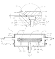
- the single wafer epitaxial wafer manufacturing apparatus includes a reaction vessel 11.
- the reaction vessel 11 has a substantially upper bowl-shaped upper dome 11a and a substantially bowl-shaped lower dome 11b, and a space is formed inside by bringing these domes 11a and 11b into close contact with each other.
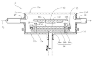
- the space inside the reaction vessel 11 is provided with a susceptor 13 that supports a single silicon wafer 12 for growing an epitaxial layer (not shown) on the surface (upper surface).
- the susceptor 13 is rotated by a rotating shaft 14. Held possible.
- the susceptor 13 is formed in a relatively thick disk shape.
- the susceptor 13 is formed with a recess 13a for accommodating the silicon wafer 12, and a ring-shaped step 13b on which the outer periphery of the silicon wafer 12 is placed is formed in the recess 13a.
- the rotary shaft 14 is rotatably inserted in the center of the lower dome 11b, and the upper surface of the rotary shaft portion 14a is concentrically provided integrally with the shaft portion 14a. And a disk-shaped receiving portion 14b for receiving the lower surface.
- the outer diameter of the receiving portion 14 b is formed slightly smaller than the outer diameter of the susceptor 13.
- the bottom wall 13c excluding the ring-shaped step portion 13b in the recess 13a of the susceptor 13 has a plurality of through holes on the same circumference centered on the axis of the rotation shaft portion 14a and at equal intervals in the circumferential direction. 13d is formed.
- a through hole 14 c is formed at a position facing the through hole 13 d of the receiving portion 14 b of the rotating shaft 14.
- the lift pin 16 is inserted into the through hole 13d and the through hole 14c.
- the lift pin 16 is provided integrally with the lift shaft portion 16a via the lift taper portion 16b on the upper surface of the lift shaft portion 16a and the lift shaft portion 16a, and has a larger diameter than the lift shaft portion 16a.
- a head portion 16c The upper surface of the lift head 16c, that is, the top 16d is formed in a spherical shape.
- the through hole 13d of the susceptor 13 has a small diameter hole portion 13e formed slightly larger in diameter than the lift shaft portion 16a of the lift pin 16, and the same taper as the lift taper portion 16b, and accommodates the lift taper portion 16b.
- the susceptor 13 is made of carbon covered with a SiC film, and the lift pins 16 are made of SiC, glassy carbon (glassy carbon), or quartz.
- the distance H between the extended surface of the upper surface of the stepped portion 13b of the susceptor 13 and the extended surface of the upper surface of the bottom wall 13c at the position of the lift pin 16 in the recess 13a of the susceptor 13 is 0.1 to 1 mm, preferably 0.2 to 0.
- the range is set to 8 mm.
- the distance H between the extended surface of the upper surface of the stepped portion 13b of the susceptor 13 and the extended surface of the upper surface of the bottom wall 13c at the position of the lift pin 16 in the recess 13a of the susceptor 13 is limited to the range of 0.1 to 1 mm. If it is less than 0.1 mm, there is a problem of contact with the lift pins 16 due to warpage of the wafer 12, and if it exceeds 1 mm, there is a problem that slip occurs.
- a gas supply port 11c and a gas discharge port 11d are disposed on the outer peripheral surface of the upper dome 11a.
- One end of a gas introduction pipe 17 for supplying a source gas and a carrier gas is connected to the gas supply port 11c, and one end of a gas discharge pipe 18 is connected to the gas discharge port 11d.
- the gas introduction pipe 17 and the gas discharge pipe 18 are formed of a hydrochloric acid resistant alloy such as Hastelloy.
- an upper lamp (not shown) is provided above the upper dome 11a, and a lower lamp (not shown) is provided below the lower dome 11b. These lamps are formed by halogen lamps, incandescent lamps, arc lamps, graphite heaters or the like.
- the reaction vessel 11 is configured such that the source gas is introduced together with the carrier gas.
- the source gas examples include SiH 2 Cl 2 , SiHCl 3 , SiH 4, and SiCl 4
- examples of the carrier gas mainly include H 2 .
- the source gas introduced from the gas introduction pipe 17 and the gas supply port 11c flows through the space between the upper dome 11a and the silicon wafer 12, and after forming an epitaxial layer made of a silicon single crystal thin film on the surface of the silicon wafer 12, The gas is discharged through the gas discharge port 11d and the gas discharge pipe 18.
- the lift pin 16 protrudes upward from the upper surface of the bottom wall 13c, and the height h of the top 16d of the lift pin 16 with respect to the upper surface of the bottom wall 13c is from a position exceeding 0 mm.
- the height h of the top 16d of the lift pin 16 is limited to a range from a position exceeding 0 mm to immediately before contacting the silicon wafer 12 of the lift pin 16 when the length of the lift pin 16 is 0 mm or less.
- the thickness of the bottom wall 13c is larger than the thickness of the bottom wall 13c, the temperature of the portion of the lift pin 16 decreases due to heat conduction, and when the lift pin 16 comes into contact with the silicon wafer 12, damage to the back surface of the wafer and generation of heat radiation from the lift pin 16 in contact with the wafer. Because there is.
- the rotating shaft 14 is lowered relative to the reaction vessel 11 (FIG. 2).
- the lower end of the lift pin 16 comes into contact with the upper surface of the lower wall 13c of the lower dome 11b, and the top 16d of the lift pin 16 projects upward from the upper surface of the susceptor 13.
- the transfer blade 19 on which the silicon wafer 12 is placed is inserted into the reaction vessel 11, the silicon wafer 12 is placed on the lift pins 16, and the silicon wafer 12 is temporarily held by the lift pins 16 (FIG. 3).
- the rotating shaft 14 is raised relative to the reaction vessel 11.
- the lower end of the lift pin 16 is separated from the upper surface of the lower wall 11e of the lower dome 11b, and the lift head portion 16c of the lift pin 16 is accommodated in the large-diameter hole portion 13g of the through hole 13d (FIG. 1).
- the lift taper portion 16b of the lift pin 16 contacts the taper hole portion 13f of the through hole 13d, and contacts the silicon wafer 12 of the lift pin 16 from a position where the height h of the top 16d of the lift pin 16 exceeds 0 mm. It becomes the range until just before.
- the lower surface of the outer peripheral portion of the silicon wafer 12 is placed on the upper surface of the stepped portion 13b, and the silicon wafer 12 is accommodated in the concave portion 13a.
- the raw material gas is introduced into the reaction vessel 11 together with the carrier gas through the gas introduction pipe 17 and the gas supply port 11c.
- the upper lamp and the lower lamp are turned on, and a carrier gas is allowed to flow into the reaction vessel 11.
- the source gas introduced together with the carrier gas reaches the surface of the silicon wafer 12, an epitaxial layer made of a silicon single crystal thin film is formed on the surface of the silicon wafer 12.
- the rotating shaft 14 is lowered relative to the reaction vessel 11.
- the lower end of the lift pin 16 comes into contact with the upper surface of the lower wall 11c of the lower dome 11b, and the top 16d of the lift pin 16 comes into contact with the lower surface of the silicon wafer 12 so that the lift pin 16 pushes up the silicon wafer 12 (FIG. 3).
- the transfer blade 19 is inserted between the silicon wafer 12 and the susceptor 13
- the blade 19 is raised to place the silicon wafer 12 on the blade 19 (FIG. 2).
- the silicon wafer 12 on which the epitaxial layer is formed can be taken out from the reaction vessel 11.
- a silicon wafer is used as the semiconductor wafer, but a GaAs wafer, InP wafer, ZnS wafer, or ZnSe wafer may be used.
- Example 1 A lamp heating horizontal single-wafer epitaxial growth apparatus (manufactured by AMAT) was prepared. First, the ratio (Wa: Wb) between the output Wa of the upper lamp and the output Wb of the lower lamp of this apparatus was set to 50:50, and a carrier gas (H 2 ) was allowed to flow. In this state, the rotating shaft 14 was lowered relative to the reaction vessel 11 (FIG. 2). As a result, the lower end of the lift pin 16 abuts on the upper surface of the lower wall 13c of the lower dome 11b, and the top 16d of the lift pin 16 protrudes upward from the upper surface of the susceptor 13.
- the lift taper portion 16b of the lift pin 16 was in contact with the taper hole portion 13f of the through hole 13d, and the height h of the top 16d of the lift pin 16 was +0.05 mm. That is, the lift pin 16 protrudes upward by 0.05 mm from the upper surface of the bottom wall 13c. Further, the lower surface of the outer peripheral portion of the silicon wafer 12 was placed on the upper surface of the stepped portion 13b, and the silicon wafer 12 was accommodated in the concave portion 13a. In this state, while maintaining the output ratio Wa: Wb of the upper lamp and the lower lamp at 50:50, the silicon wafer 12 is heated with these lamps, and the gas is introduced into the reaction vessel 11 through the gas introduction pipe 17 and the gas supply port 11c.
- a source gas (SiHCl 3 ) was introduced together with a carrier gas (H 2 ), and an epitaxial layer made of a single crystal silicon thin film having a thickness of 3 ⁇ m was formed on the surface of the silicon wafer 12 to produce an epitaxial wafer.
- the distance H between the extended surface of the upper surface of the stepped portion 13b of the susceptor 13 and the extended surface of the upper surface of the bottom wall 13c at the position of the lift pin 16 in the concave portion 13a of the susceptor 13 is 0.3 mm.
- the temperature measured by a thermometer was 1100 ° C.
- Example 2 An epitaxial wafer was produced in the same manner as in Example 1 except that the ratio (Wa: Wb) of the upper lamp output Wa to the lower lamp output Wb was set to 55:45.
- Example 3 The height h of the top of the lift pin when the lift head of the lift pin was accommodated in the large-diameter hole of the through hole was +0.12 mm (the lift pin protruded upward by 0.12 mm from the top of the bottom wall) Except for this, an epitaxial wafer was produced in the same manner as in Example 1.
- Example 4 The head of the lift pin when the ratio of the output Wa of the upper lamp to the output Wb of the lower lamp (Wa: Wb) is set to 55:45 and the lift head of the lift pin is accommodated in the large-diameter hole of the through hole
- An epitaxial wafer was manufactured in the same manner as in Example 1 except that the height h of the top was +0.12 mm (the lift pins protruded upward by 0.12 mm from the upper surface of the bottom wall).
- ⁇ Comparative example 4> Lift pin head when the ratio of the upper lamp output Wa to the lower lamp output Wb (Wa: Wb) is set to 46:54, and the lift head of the lift pin is accommodated in the large-diameter hole of the through hole.
- An epitaxial wafer was manufactured in the same manner as in Example 1 except that the height h of the top was +0.12 mm (the lift pins protruded upward by 0.12 mm from the upper surface of the bottom wall).
- Epitaxial wafer was prepared in the same manner as in Example 1 except that the height h of the top was ⁇ 0.7 mm (the top of the lift pin was pulled into the through hole by 0.7 mm from the top of the bottom wall). did.
- the backside deposition refers to a phenomenon in which the silicon film covering the susceptor surface is peeled off by the hydrochloric acid component in the source gas (SiHCl 3 ) and attached to the back side on the high temperature side of the silicon wafer. This backside deposition was judged by the difference between the thickness of the silicon wafer before forming the epitaxial layer and the thickness of the epitaxial wafer after forming the epitaxial layer.
- Ref is backside deposition when the ratio (Wa: Wb) of the upper lamp output Wa to the lower lamp output Wb is set to 42:58, ie, Comparative Example 1. 3, 5, 7, and 11 are used as reference values.
- B indicates that the backside deposition was reduced by less than 20% from the reference value
- A indicates that the backside deposition was 20% or more and less than 40% from the reference value.
- AA indicates that the rear surface deposition is extremely greatly reduced to 40% or more and less than 65% from the reference value.
- nanotopography is an index representing the flatness of the epitaxial layer surface of an epitaxial wafer.
- This nanotopography was measured with a nanomapper (manufactured by ADE).
- A indicates that the unevenness was as small as less than 5 nm
- B indicates that the unevenness was more than 5 nm and less than 10 nm
- BB indicates the unevenness. Is very large at 10 nm or more.
- the present invention can be used to form an epitaxial layer on the surface of a semiconductor wafer such as a silicon wafer placed on a susceptor in a reaction vessel while holding it with a holder and rotating it.
- a semiconductor wafer such as a silicon wafer placed on a susceptor in a reaction vessel while holding it with a holder and rotating it.
Landscapes
- Chemical & Material Sciences (AREA)
- Engineering & Computer Science (AREA)
- Materials Engineering (AREA)
- Metallurgy (AREA)
- Organic Chemistry (AREA)
- General Chemical & Material Sciences (AREA)
- Chemical Kinetics & Catalysis (AREA)
- Mechanical Engineering (AREA)
- Crystallography & Structural Chemistry (AREA)
- Inorganic Chemistry (AREA)
- Physics & Mathematics (AREA)
- Condensed Matter Physics & Semiconductors (AREA)
- General Physics & Mathematics (AREA)
- Manufacturing & Machinery (AREA)
- Computer Hardware Design (AREA)
- Microelectronics & Electronic Packaging (AREA)
- Power Engineering (AREA)
- Container, Conveyance, Adherence, Positioning, Of Wafer (AREA)
- Chemical Vapour Deposition (AREA)
Abstract
Description
ランプ加熱方式の横型枚葉式エピタキシャル成長装置(AMAT社製)を用意した。先ずこの装置の上側ランプの出力Waと下側ランプの出力Wbとの比(Wa:Wb)を50:50に設定し、キャリアガス(H2)を流した。この状態で回転軸14を反応容器11に対して相対的に下降させた(図2)。これによりリフトピン16の下端が下側ドーム11bの下壁13c上面に当接し、リフトピン16の頭頂部16dがサセプタ13の上面より上方に突出した。この状態で結晶の面方位が<100>である直径300mmのp型シリコンウェーハ12を載せた搬送用ブレード19を反応容器11に挿入し、シリコンウェーハ12をリフトピン16上に置いてリフトピン16によりシリコンウェーハ12を一時的に保持させた(図3)。次に回転軸14を反応容器11に対して相対的に上昇させた。これによりリフトピン16の下端が下側ドーム11bの下壁11e上面から離れ、リフトピン16のリフト用頭部16cが貫通孔13dの大径孔部13gに収容された(図1)。このときリフトピン16のリフト用テーパ部16bが貫通孔13dのテーパ孔部13fに接触して、リフトピン16の頭頂部16dの高さhが+0.05mmであった。即ち、リフトピン16が底壁13c上面より0.05mmだけ上方に突出した。またシリコンウェーハ12はその外周部下面が段差部13b上面に載り、シリコンウェーハ12が凹部13aに収容された。この状態で上側ランプ及び下側ランプの出力比Wa:Wbを50:50に保ったままこれらのランプでシリコンウェーハ12を加熱しながら、ガス導入管17及びガス供給口11cを通して反応容器11内に原料ガス(SiHCl3)をキャリアガス(H2)とともに導入し、シリコンウェーハ12表面に厚さ3μmのシリコン単結晶薄膜からなるエピタキシャル層を形成してエピタキシャルウェーハを作製した。なお、サセプタ13の段差部13b上面の延長面とサセプタ13の凹部13aのうちリフトピン16位置での底壁13c上面の延長面との距離Hが0.3mmであり、シリコンウェーハの中央部における放射温度計による温度は1100℃であった。 <Example 1>
A lamp heating horizontal single-wafer epitaxial growth apparatus (manufactured by AMAT) was prepared. First, the ratio (Wa: Wb) between the output Wa of the upper lamp and the output Wb of the lower lamp of this apparatus was set to 50:50, and a carrier gas (H 2 ) was allowed to flow. In this state, the rotating
上側ランプの出力Waと下側ランプの出力Wbとの比(Wa:Wb)を55:45に設定したこと以外は、実施例1と同様にしてエピタキシャルウェーハを作製した。 <Example 2>
An epitaxial wafer was produced in the same manner as in Example 1 except that the ratio (Wa: Wb) of the upper lamp output Wa to the lower lamp output Wb was set to 55:45.
リフトピンのリフト用頭部を貫通孔の大径孔部に収容したときのリフトピンの頭頂部の高さhが+0.12mmであった(リフトピンが底壁上面より0.12mmだけ上方に突出した)こと以外は、実施例1と同様にしてエピタキシャルウェーハを作製した。 <Example 3>
The height h of the top of the lift pin when the lift head of the lift pin was accommodated in the large-diameter hole of the through hole was +0.12 mm (the lift pin protruded upward by 0.12 mm from the top of the bottom wall) Except for this, an epitaxial wafer was produced in the same manner as in Example 1.
上側ランプの出力Waと下側ランプの出力Wbとの比(Wa:Wb)を55:45に設定し、リフトピンのリフト用頭部を貫通孔の大径孔部に収容したときのリフトピンの頭頂部の高さhが+0.12mmであった(リフトピンが底壁上面より0.12mmだけ上方に突出した)こと以外は、実施例1と同様にしてエピタキシャルウェーハを作製した。 <Example 4>
The head of the lift pin when the ratio of the output Wa of the upper lamp to the output Wb of the lower lamp (Wa: Wb) is set to 55:45 and the lift head of the lift pin is accommodated in the large-diameter hole of the through hole An epitaxial wafer was manufactured in the same manner as in Example 1 except that the height h of the top was +0.12 mm (the lift pins protruded upward by 0.12 mm from the upper surface of the bottom wall).
上側ランプの出力Waと下側ランプの出力Wbとの比(Wa:Wb)を42:58に設定したこと以外は、実施例1と同様にしてエピタキシャルウェーハを作製した。 <Comparative Example 1>
An epitaxial wafer was fabricated in the same manner as in Example 1 except that the ratio (Wa: Wb) of the upper lamp output Wa to the lower lamp output Wb was set to 42:58.
上側ランプの出力Waと下側ランプの出力Wbとの比(Wa:Wb)を46:54に設定したこと以外は、実施例1と同様にしてエピタキシャルウェーハを作製した。 <Comparative example 2>
An epitaxial wafer was fabricated in the same manner as in Example 1 except that the ratio (Wa: Wb) of the upper lamp output Wa to the lower lamp output Wb was set to 46:54.
上側ランプの出力Waと下側ランプの出力Wbとの比(Wa:Wb)を42:58に設定し、リフトピンのリフト用頭部を貫通孔の大径孔部に収容したときのリフトピンの頭頂部の高さhが+0.12mmであった(リフトピンが底壁上面より0.12mmだけ上方に突出した)こと以外は、実施例1と同様にしてエピタキシャルウェーハを作製した。 <Comparative Example 3>
The lift pin head when the ratio (Wa: Wb) of the upper lamp output Wa to the lower lamp output Wb is set to 42:58 and the lift head of the lift pin is accommodated in the large-diameter hole of the through hole. An epitaxial wafer was manufactured in the same manner as in Example 1 except that the height h of the top was +0.12 mm (the lift pins protruded upward by 0.12 mm from the upper surface of the bottom wall).
上側ランプの出力Waと下側ランプの出力Wbとの比(Wa:Wb)を46:54に設定し、リフトピンのリフト用頭部を貫通孔の大径孔部に収容したときのリフトピンの頭頂部の高さhが+0.12mmであった(リフトピンが底壁上面より0.12mmだけ上方に突出した)こと以外は、実施例1と同様にしてエピタキシャルウェーハを作製した。 <Comparative example 4>
Lift pin head when the ratio of the upper lamp output Wa to the lower lamp output Wb (Wa: Wb) is set to 46:54, and the lift head of the lift pin is accommodated in the large-diameter hole of the through hole. An epitaxial wafer was manufactured in the same manner as in Example 1 except that the height h of the top was +0.12 mm (the lift pins protruded upward by 0.12 mm from the upper surface of the bottom wall).
上側ランプの出力Waと下側ランプの出力Wbとの比(Wa:Wb)を42:58に設定し、リフトピンのリフト用頭部を貫通孔の大径孔部に収容したときのリフトピンの頭頂部の高さhが+0.25mmであり(リフトピンが底壁上面より0.25mmだけ上方に突出した)、リフトピンの頭頂部がシリコンウェーハの裏面に接触したこと以外は、実施例1と同様にしてエピタキシャルウェーハを作製した。 <Comparative Example 5>
The lift pin head when the ratio (Wa: Wb) of the upper lamp output Wa to the lower lamp output Wb is set to 42:58 and the lift head of the lift pin is accommodated in the large-diameter hole of the through hole. The height h of the top is +0.25 mm (the lift pin protrudes upward by 0.25 mm from the top surface of the bottom wall), and the top of the lift pin is in contact with the back surface of the silicon wafer. An epitaxial wafer was prepared.
上側ランプの出力Waと下側ランプの出力Wbとの比(Wa:Wb)を55:45に設定し、リフトピンのリフト用頭部を貫通孔の大径孔部に収容したときのリフトピンの頭頂部の高さhが+0.25mmであり(リフトピンが底壁上面より0.25mmだけ上方に突出した)、リフトピンの頭頂部がシリコンウェーハの裏面に接触したこと以外は、実施例1と同様にしてエピタキシャルウェーハを作製した。 <Comparative Example 6>
The head of the lift pin when the ratio of the output Wa of the upper lamp to the output Wb of the lower lamp (Wa: Wb) is set to 55:45 and the lift head of the lift pin is accommodated in the large-diameter hole of the through hole The height h of the top is +0.25 mm (the lift pin protrudes upward by 0.25 mm from the top surface of the bottom wall), and the top of the lift pin is in contact with the back surface of the silicon wafer. An epitaxial wafer was prepared.
上側ランプの出力Waと下側ランプの出力Wbとの比(Wa:Wb)を42:58に設定し、リフトピンのリフト用頭部を貫通孔の大径孔部に収容したときのリフトピンの頭頂部の高さhが-0.7mmであった(リフトピンの頭頂部が底壁上面より0.7mmだけ貫通孔内に引込んだ)こと以外は、実施例1と同様にしてエピタキシャルウェーハを作製した。 <Comparative Example 7>
The lift pin head when the ratio (Wa: Wb) of the upper lamp output Wa to the lower lamp output Wb is set to 42:58 and the lift head of the lift pin is accommodated in the large-diameter hole of the through hole. Epitaxial wafer was prepared in the same manner as in Example 1 except that the height h of the top was −0.7 mm (the top of the lift pin was pulled into the through hole by 0.7 mm from the top of the bottom wall). did.
上側ランプの出力Waと下側ランプの出力Wbとの比(Wa:Wb)を46:54に設定し、リフトピンのリフト用頭部を貫通孔の大径孔部に収容したときのリフトピンの頭頂部の高さhが-0.7mmであった(リフトピンの頭頂部が底壁上面より0.7mmだけ貫通孔内に引込んだ)こと以外は、実施例1と同様にしてエピタキシャルウェーハを作製した。 <Comparative Example 8>
Lift pin head when the ratio of the upper lamp output Wa to the lower lamp output Wb (Wa: Wb) is set to 46:54, and the lift head of the lift pin is accommodated in the large-diameter hole of the through hole. Epitaxial wafer was prepared in the same manner as in Example 1 except that the height h of the top was −0.7 mm (the top of the lift pin was pulled into the through hole by 0.7 mm from the top of the bottom wall). did.
リフトピンのリフト用頭部を貫通孔の大径孔部に収容したときのリフトピンの頭頂部の高さhが-0.7mmであった(リフトピンの頭頂部が底壁上面より0.7mmだけ貫通孔内に引込んだ)こと以外は、実施例1と同様にしてエピタキシャルウェーハを作製した。 <Comparative Example 9>
The height h of the top of the lift pin when the lift head of the lift pin was accommodated in the large-diameter hole of the through hole was −0.7 mm (the top of the lift pin penetrated 0.7 mm from the top of the bottom wall). An epitaxial wafer was produced in the same manner as in Example 1 except that the wafer was drawn into the hole.
上側ランプの出力Waと下側ランプの出力Wbとの比(Wa:Wb)を55:45に設定し、リフトピンのリフト用頭部を貫通孔の大径孔部に収容したときのリフトピンの頭頂部の高さhが-0.7mmであった(リフトピンの頭頂部が底壁上面より0.7mmだけ貫通孔内に引込んだ)こと以外は、実施例1と同様にしてエピタキシャルウェーハを作製した。 <Comparative Example 10>
The head of the lift pin when the ratio of the output Wa of the upper lamp to the output Wb of the lower lamp (Wa: Wb) is set to 55:45 and the lift head of the lift pin is accommodated in the large-diameter hole of the through hole Epitaxial wafer was prepared in the same manner as in Example 1 except that the height h of the top was −0.7 mm (the top of the lift pin was pulled into the through hole by 0.7 mm from the top of the bottom wall). did.
上側ランプの出力Waと下側ランプの出力Wbとの比(Wa:Wb)を42:58に設定し、リフトピンのリフト用頭部を貫通孔の大径孔部に収容したときのリフトピンの頭頂部の高さhが0mmであった(リフトピンの頭頂部が底壁上面と一致した)こと以外は、実施例1と同様にしてエピタキシャルウェーハを作製した。 <Comparative Example 11>
The lift pin head when the ratio (Wa: Wb) of the upper lamp output Wa to the lower lamp output Wb is set to 42:58 and the lift head of the lift pin is accommodated in the large-diameter hole of the through hole. An epitaxial wafer was produced in the same manner as in Example 1 except that the height h of the top was 0 mm (the top of the lift pin coincided with the upper surface of the bottom wall).
上側ランプの出力Waと下側ランプの出力Wbとの比(Wa:Wb)を46:54に設定し、リフトピンのリフト用頭部を貫通孔の大径孔部に収容したときのリフトピンの頭頂部の高さhが0mmであった(リフトピンの頭頂部が底壁上面と一致した)こと以外は、実施例1と同様にしてエピタキシャルウェーハを作製した。 <Comparative Example 12>
Lift pin head when the ratio of the upper lamp output Wa to the lower lamp output Wb (Wa: Wb) is set to 46:54, and the lift head of the lift pin is accommodated in the large-diameter hole of the through hole. An epitaxial wafer was produced in the same manner as in Example 1 except that the height h of the top was 0 mm (the top of the lift pin coincided with the upper surface of the bottom wall).
リフトピンのリフト用頭部を貫通孔の大径孔部に収容したときのリフトピンの頭頂部の高さhが0mmであった(リフトピンの頭頂部が底壁上面と一致した)こと以外は、実施例1と同様にしてエピタキシャルウェーハを作製した。 <Comparative Example 13>
Except that the height h of the top of the lift pin when the lift head of the lift pin was accommodated in the large-diameter hole of the through hole was 0 mm (the top of the lift pin coincided with the top of the bottom wall). An epitaxial wafer was produced in the same manner as in Example 1.
上側ランプの出力Waと下側ランプの出力Wbとの比(Wa:Wb)を55:45に設定し、リフトピンのリフト用頭部を貫通孔の大径孔部に収容したときのリフトピンの頭頂部の高さhが0mmであった(リフトピンの頭頂部が底壁上面と一致した)こと以外は、実施例1と同様にしてエピタキシャルウェーハを作製した。 <Comparative example 14>
The head of the lift pin when the ratio of the output Wa of the upper lamp to the output Wb of the lower lamp (Wa: Wb) is set to 55:45 and the lift head of the lift pin is accommodated in the large-diameter hole of the through hole An epitaxial wafer was produced in the same manner as in Example 1 except that the height h of the top was 0 mm (the top of the lift pin coincided with the upper surface of the bottom wall).
実施例1~4及び比較例1~14のエピタキシャルウェーハについて、裏面デポジションとナノトポグラフィを測定した。その結果を表1に示す。ここで、裏面デポジションとは、サセプタ表面を被覆するシリコン膜が原料ガス(SiHCl3)中の塩酸成分により剥がれてシリコンウェーハの高温側の裏面に付着する現象をいう。この裏面デポジションは、エピタキシャル層を形成する前のシリコンウェーハの厚さと、エピタキシャル層を形成した後のエピタキシャルウェーハの厚さとの相違により判断した。表1の裏面デポジションの欄において『Ref』は上側ランプの出力Waと下側ランプの出力Wbとの比(Wa:Wb)を42:58に設定したときの裏面デポジション、即ち比較例1、3、5、7及び11の裏面デポジションを基準値とすることを示す。また表1の裏面デポジションの欄において『B』は裏面デポジションが基準値より20%未満しか低減しなかったことを示し、『A』は裏面デポジションが基準値より20%以上40%未満と比較的大幅に低減したことを示し、『AA』は裏面デポジションが基準値より40%以上65%未満と極めて大幅に低減したことを示す。一方、ナノトポグラフィとは、エピタキシャルウェーハのエピタキシャル層表面の平坦度を表す指標である。このナノトポグラフィはナノマッパー(Nanomapper:ADE社製)により測定した。表1のナノトポグラフィの欄において『A』は凹凸が5nm未満と小さかったことを示し、『B』は凹凸が5nmを超え10nm以下と比較的大きかったであることを示し、『BB』は凹凸が10nm以上と極めて大きかったことを示す。 <
The epitaxial wafers of Examples 1 to 4 and Comparative Examples 1 to 14 were measured for backside deposition and nanotopography. The results are shown in Table 1. Here, the backside deposition refers to a phenomenon in which the silicon film covering the susceptor surface is peeled off by the hydrochloric acid component in the source gas (SiHCl 3 ) and attached to the back side on the high temperature side of the silicon wafer. This backside deposition was judged by the difference between the thickness of the silicon wafer before forming the epitaxial layer and the thickness of the epitaxial wafer after forming the epitaxial layer. In the column of backside deposition in Table 1, “Ref” is backside deposition when the ratio (Wa: Wb) of the upper lamp output Wa to the lower lamp output Wb is set to 42:58, ie, Comparative Example 1. 3, 5, 7, and 11 are used as reference values. Also, in the column for backside deposition in Table 1, “B” indicates that the backside deposition was reduced by less than 20% from the reference value, and “A” indicates that the backside deposition was 20% or more and less than 40% from the reference value. “AA” indicates that the rear surface deposition is extremely greatly reduced to 40% or more and less than 65% from the reference value. On the other hand, nanotopography is an index representing the flatness of the epitaxial layer surface of an epitaxial wafer. This nanotopography was measured with a nanomapper (manufactured by ADE). In the column of nanotopography in Table 1, “A” indicates that the unevenness was as small as less than 5 nm, “B” indicates that the unevenness was more than 5 nm and less than 10 nm, and “BB” indicates the unevenness. Is very large at 10 nm or more.

Claims (8)
- 凹部とこの凹部内に形成されたリング状の段差部とを有し、前記凹部のうち前記段差部を除く底壁に複数の貫通孔が形成されたサセプタを反応容器内に配置し、前記貫通孔に挿通されたリフトピンでウェーハを一時的に保持した後に前記ウェーハの外周部下面を前記段差部に載せることにより前記ウェーハを前記凹部に収容し、原料ガスを前記反応容器に流通させることにより前記凹部に収容された前記ウェーハの表面にエピタキシャル層を形成するエピタキシャルウェーハの製造方法において、
前記エピタキシャル層を前記ウェーハ表面に形成するときに、前記リフトピンが前記底壁上面より上方に突出し、前記底壁上面を基準とする前記リフトピンの頭頂部の高さhを0mmを超えた位置から前記リフトピンの前記ウェーハに接触する直前までの範囲に設定することを特徴とするエピタキシャルウェーハの製造方法。 A susceptor having a concave portion and a ring-shaped step portion formed in the concave portion and having a plurality of through holes formed in a bottom wall of the concave portion excluding the step portion is disposed in the reaction vessel, After temporarily holding the wafer with lift pins inserted through holes, the wafer is accommodated in the recess by placing the lower surface of the outer peripheral portion on the stepped portion, and the source gas is circulated through the reaction vessel. In an epitaxial wafer manufacturing method for forming an epitaxial layer on the surface of the wafer housed in a recess,
When the epitaxial layer is formed on the wafer surface, the lift pin protrudes above the bottom wall upper surface, and the height h of the top of the lift pin relative to the bottom wall upper surface exceeds 0 mm. A method for producing an epitaxial wafer, wherein the lift pins are set to a range immediately before contacting the wafer. - サセプタの段差部上面の延長面と前記サセプタの凹部のうちリフトピン位置での底壁上面の延長面との距離Hが0.1~1mmである請求項1記載のエピタキシャルウェーハの製造方法。 The method for producing an epitaxial wafer according to claim 1, wherein the distance H between the extended surface of the upper surface of the stepped portion of the susceptor and the extended surface of the upper surface of the bottom wall at the lift pin position in the concave portion of the susceptor is 0.1 to 1 mm.
- エピタキシャル層をウェーハ表面に形成するときに、リフトピンが底壁上面より上方に突出し、前記底壁上面を基準とする前記リフトピンの頭頂部の高さhを0.05mm以上かつ前記リフトピンの前記ウェーハに接触する直前までの範囲に設定する請求項1記載のエピタキシャルウェーハの製造方法。 When the epitaxial layer is formed on the wafer surface, the lift pins protrude above the top surface of the bottom wall, the height h of the top of the lift pins relative to the top surface of the bottom wall is 0.05 mm or more, and the lift pins are formed on the wafer. The method for manufacturing an epitaxial wafer according to claim 1, wherein the range is set to a range immediately before contact.
- サセプタをSiC膜により被覆されたカーボンにより形成し、リフトピンをSiC、グラシーカーボン又は石英のいずれかにより形成した請求項1ないし3いずれか1項に記載のエピタキシャルウェーハの製造方法。 The method for producing an epitaxial wafer according to any one of claims 1 to 3, wherein the susceptor is formed of carbon coated with a SiC film, and the lift pins are formed of SiC, glassy carbon, or quartz.
- 凹部とこの凹部内に形成されたリング状の段差部とを有し前記凹部のうち前記段差部を除く底壁に複数の貫通孔が形成されかつ反応容器内に配置されたサセプタと、前記貫通孔に挿通されウェーハを一時的に保持するリフトピンとを備え、前記ウェーハを前記リフトピンで一時的に保持した後に前記ウェーハの外周部下面を前記段差部に載せることにより前記ウェーハが前記凹部に収容され、原料ガスを前記反応容器に流通させることにより前記凹部に収容された前記ウェーハの表面にエピタキシャル層が形成されるウェーハの保持具において、
前記エピタキシャル層が前記ウェーハ表面に形成されるときに、前記リフトピンが前記底壁上面より上方に突出し、前記底壁上面を基準とする前記リフトピンの頭頂部の高さhが0mmを超えた位置から前記リフトピンの前記ウェーハに接触する直前までの範囲に設定されたことを特徴とするウェーハの保持具。 A susceptor having a recess and a ring-shaped step formed in the recess, wherein a plurality of through holes are formed in a bottom wall of the recess excluding the step, and the susceptor is disposed in a reaction vessel; And a lift pin that is inserted into the hole and temporarily holds the wafer, and after the wafer is temporarily held by the lift pin, the lower surface of the outer peripheral portion of the wafer is placed on the step portion so that the wafer is accommodated in the recess. In a wafer holder in which an epitaxial layer is formed on the surface of the wafer accommodated in the recess by flowing a source gas through the reaction vessel,
When the epitaxial layer is formed on the wafer surface, the lift pin protrudes above the bottom wall upper surface, and the height h of the top of the lift pin relative to the bottom wall upper surface exceeds 0 mm. A wafer holder, wherein the lift pin is set in a range immediately before contacting the wafer. - サセプタの段差部上面の延長面と前記サセプタの凹部のうちリフトピン位置での底壁上面の延長面との距離Hが0.1~1mmである請求項5記載のウェーハの保持具。 6. The wafer holder according to claim 5, wherein a distance H between an extended surface of the upper surface of the stepped portion of the susceptor and an extended surface of the upper surface of the bottom wall at the lift pin position in the concave portion of the susceptor is 0.1 to 1 mm.
- エピタキシャル層がウェーハ表面に形成されるときに、リフトピンが底壁上面より上方に突出し、前記底壁上面を基準とする前記リフトピンの頭頂部の高さhが0.05mm以上かつ前記リフトピンの前記ウェーハに接触する直前までの範囲に設定される請求項5記載のウェーハの保持具。 When the epitaxial layer is formed on the wafer surface, the lift pins protrude above the upper surface of the bottom wall, the height h of the top of the lift pins with respect to the upper surface of the bottom wall is 0.05 mm or more, and the wafer of the lift pins The wafer holder according to claim 5, wherein the wafer holder is set in a range up to immediately before contacting the wafer.
- サセプタがSiC膜により被覆されたカーボンにより形成され、リフトピンがSiC、グラシーカーボン又は石英のいずれかにより形成された請求項5ないし7いずれか1項に記載のウェーハの保持具。 The wafer holder according to any one of claims 5 to 7, wherein the susceptor is formed of carbon coated with a SiC film, and the lift pins are formed of SiC, glassy carbon, or quartz.
Priority Applications (2)
| Application Number | Priority Date | Filing Date | Title |
|---|---|---|---|
| DE112009001826.2T DE112009001826B4 (en) | 2008-07-31 | 2009-07-24 | Production process for an epitaxial wafer and the holding device used to hold the wafer |
| US13/003,440 US8980001B2 (en) | 2008-07-31 | 2009-07-24 | Method for manufacturing epitaxial wafer and wafer holder used in the method |
Applications Claiming Priority (2)
| Application Number | Priority Date | Filing Date | Title |
|---|---|---|---|
| JP2008197723A JP5412759B2 (en) | 2008-07-31 | 2008-07-31 | Epitaxial wafer holder and method for manufacturing the wafer |
| JP2008-197723 | 2008-07-31 |
Publications (1)
| Publication Number | Publication Date |
|---|---|
| WO2010013646A1 true WO2010013646A1 (en) | 2010-02-04 |
Family
ID=41610345
Family Applications (1)
| Application Number | Title | Priority Date | Filing Date |
|---|---|---|---|
| PCT/JP2009/063243 WO2010013646A1 (en) | 2008-07-31 | 2009-07-24 | Method for manufacturing epitaxial wafer and wafer holder used in the method |
Country Status (4)
| Country | Link |
|---|---|
| US (1) | US8980001B2 (en) |
| JP (1) | JP5412759B2 (en) |
| DE (1) | DE112009001826B4 (en) |
| WO (1) | WO2010013646A1 (en) |
Cited By (1)
| Publication number | Priority date | Publication date | Assignee | Title |
|---|---|---|---|---|
| WO2016098510A1 (en) * | 2014-12-19 | 2016-06-23 | 信越半導体株式会社 | Epitaxial wafer manufacturing method |
Families Citing this family (18)
| Publication number | Priority date | Publication date | Assignee | Title |
|---|---|---|---|---|
| JP5698043B2 (en) * | 2010-08-04 | 2015-04-08 | 株式会社ニューフレアテクノロジー | Semiconductor manufacturing equipment |
| CN102747418B (en) * | 2012-07-25 | 2015-12-16 | 东莞市天域半导体科技有限公司 | A kind of high temperature big area Device for epitaxial growth of silicon carbide and treatment process |
| JP6017328B2 (en) * | 2013-01-22 | 2016-10-26 | 東京エレクトロン株式会社 | Mounting table and plasma processing apparatus |
| JP5999511B2 (en) * | 2013-08-26 | 2016-09-28 | 信越半導体株式会社 | Vapor phase epitaxial growth apparatus and epitaxial wafer manufacturing method using the same |
| KR101548903B1 (en) | 2015-03-19 | 2015-09-04 | (주)코미코 | Lift pin and method for manufacturing the same |
| JP6424726B2 (en) | 2015-04-27 | 2018-11-21 | 株式会社Sumco | Susceptor and epitaxial growth apparatus |
| TWI615917B (en) * | 2015-04-27 | 2018-02-21 | Sumco股份有限公司 | Susceptor and epitaxial growth device |
| JP6539929B2 (en) * | 2015-12-21 | 2019-07-10 | 昭和電工株式会社 | Wafer supporting mechanism, chemical vapor deposition apparatus and method of manufacturing epitaxial wafer |
| JP6500792B2 (en) * | 2016-01-25 | 2019-04-17 | 株式会社Sumco | Method of evaluating quality of epitaxial wafer and method of manufacturing the same |
| CN108886014B (en) * | 2016-03-28 | 2023-08-08 | 应用材料公司 | Base support |
| TWI729101B (en) * | 2016-04-02 | 2021-06-01 | 美商應用材料股份有限公司 | Apparatus and methods for wafer rotation in carousel susceptor |
| JP2018026503A (en) * | 2016-08-12 | 2018-02-15 | 株式会社Sumco | Susceptor, epitaxial growth system, and manufacturing method of epitaxial wafer |
| US20180102247A1 (en) * | 2016-10-06 | 2018-04-12 | Asm Ip Holding B.V. | Substrate processing apparatus and method of manufacturing semiconductor device |
| CN106607320B (en) * | 2016-12-22 | 2019-10-01 | 武汉华星光电技术有限公司 | Thermal vacuum drying device suitable for flexible base board |
| KR102262311B1 (en) * | 2017-02-02 | 2021-06-07 | 가부시키가이샤 사무코 | A lift pin, an epitaxial growth apparatus using the lift pin, and a method for manufacturing a silicon epitaxial wafer |
| US10755955B2 (en) * | 2018-02-12 | 2020-08-25 | Applied Materials, Inc. | Substrate transfer mechanism to reduce back-side substrate contact |
| US11121019B2 (en) | 2018-06-19 | 2021-09-14 | Kla Corporation | Slotted electrostatic chuck |
| KR102640172B1 (en) | 2019-07-03 | 2024-02-23 | 삼성전자주식회사 | Processing apparatus for a substrate and method of driving the same |
Citations (6)
| Publication number | Priority date | Publication date | Assignee | Title |
|---|---|---|---|---|
| JP2000026192A (en) * | 1998-04-28 | 2000-01-25 | Shin Etsu Handotai Co Ltd | Equipment for growing thin film |
| JP2000323556A (en) * | 1999-05-13 | 2000-11-24 | Komatsu Electronic Metals Co Ltd | Epitaxial wafer manufacturing apparatus |
| WO2005034219A1 (en) * | 2003-10-01 | 2005-04-14 | Shin-Etsu Handotai Co., Ltd. | Production method for silicon epitaxial wafer, and silicon epitaxial wafer |
| JP2005311108A (en) * | 2004-04-22 | 2005-11-04 | Shin Etsu Handotai Co Ltd | Vapor phase epitaxial growth system |
| JP2007235116A (en) * | 2006-01-31 | 2007-09-13 | Tokyo Electron Ltd | Substrate mounting stage and substrate processing apparatus |
| JP2007273623A (en) * | 2006-03-30 | 2007-10-18 | Sumco Techxiv株式会社 | Method and device for manufacturing epitaxial wafer |
Family Cites Families (10)
| Publication number | Priority date | Publication date | Assignee | Title |
|---|---|---|---|---|
| US6596086B1 (en) * | 1998-04-28 | 2003-07-22 | Shin-Etsu Handotai Co., Ltd. | Apparatus for thin film growth |
| JP2001313329A (en) * | 2000-04-28 | 2001-11-09 | Applied Materials Inc | Wafer support device in semiconductor manufacturing apparatus |
| TWI307912B (en) * | 2001-05-30 | 2009-03-21 | Asm Inc | Low temperature load and bake |
| US20030178145A1 (en) * | 2002-03-25 | 2003-09-25 | Applied Materials, Inc. | Closed hole edge lift pin and susceptor for wafer process chambers |
| JP3908112B2 (en) * | 2002-07-29 | 2007-04-25 | Sumco Techxiv株式会社 | Susceptor, epitaxial wafer manufacturing apparatus and epitaxial wafer manufacturing method |
| US20070089836A1 (en) * | 2005-10-24 | 2007-04-26 | Applied Materials, Inc. | Semiconductor process chamber |
| KR100993466B1 (en) * | 2006-01-31 | 2010-11-09 | 도쿄엘렉트론가부시키가이샤 | Substrate processing apparatus and member exposed to plasma |
| US8021484B2 (en) * | 2006-03-30 | 2011-09-20 | Sumco Techxiv Corporation | Method of manufacturing epitaxial silicon wafer and apparatus therefor |
| JP2010016312A (en) * | 2008-07-07 | 2010-01-21 | Sumco Corp | Method for manufacturing epitaxial wafer |
| JP5141541B2 (en) * | 2008-12-24 | 2013-02-13 | 株式会社Sumco | Epitaxial wafer manufacturing method |
-
2008
- 2008-07-31 JP JP2008197723A patent/JP5412759B2/en active Active
-
2009
- 2009-07-24 WO PCT/JP2009/063243 patent/WO2010013646A1/en active Application Filing
- 2009-07-24 US US13/003,440 patent/US8980001B2/en active Active
- 2009-07-24 DE DE112009001826.2T patent/DE112009001826B4/en active Active
Patent Citations (6)
| Publication number | Priority date | Publication date | Assignee | Title |
|---|---|---|---|---|
| JP2000026192A (en) * | 1998-04-28 | 2000-01-25 | Shin Etsu Handotai Co Ltd | Equipment for growing thin film |
| JP2000323556A (en) * | 1999-05-13 | 2000-11-24 | Komatsu Electronic Metals Co Ltd | Epitaxial wafer manufacturing apparatus |
| WO2005034219A1 (en) * | 2003-10-01 | 2005-04-14 | Shin-Etsu Handotai Co., Ltd. | Production method for silicon epitaxial wafer, and silicon epitaxial wafer |
| JP2005311108A (en) * | 2004-04-22 | 2005-11-04 | Shin Etsu Handotai Co Ltd | Vapor phase epitaxial growth system |
| JP2007235116A (en) * | 2006-01-31 | 2007-09-13 | Tokyo Electron Ltd | Substrate mounting stage and substrate processing apparatus |
| JP2007273623A (en) * | 2006-03-30 | 2007-10-18 | Sumco Techxiv株式会社 | Method and device for manufacturing epitaxial wafer |
Cited By (4)
| Publication number | Priority date | Publication date | Assignee | Title |
|---|---|---|---|---|
| WO2016098510A1 (en) * | 2014-12-19 | 2016-06-23 | 信越半導体株式会社 | Epitaxial wafer manufacturing method |
| JP2016119380A (en) * | 2014-12-19 | 2016-06-30 | 信越半導体株式会社 | Epitaxial wafer manufacturing method |
| TWI629712B (en) * | 2014-12-19 | 2018-07-11 | 信越半導體股份有限公司 | Method for manufacturing epitaxial wafer |
| US10119193B2 (en) | 2014-12-19 | 2018-11-06 | Shin-Etsu Handotai Co., Ltd. | Method of manufacturing an epitaxial wafer comprising measuring a level difference between a front surface of a susceptor and an upper surface of a lift pin and adjusting a ratio of the heat source output |
Also Published As
| Publication number | Publication date |
|---|---|
| DE112009001826B4 (en) | 2016-02-25 |
| DE112009001826T5 (en) | 2011-06-09 |
| JP2010034476A (en) | 2010-02-12 |
| US20110114014A1 (en) | 2011-05-19 |
| US8980001B2 (en) | 2015-03-17 |
| JP5412759B2 (en) | 2014-02-12 |
Similar Documents
| Publication | Publication Date | Title |
|---|---|---|
| JP5412759B2 (en) | Epitaxial wafer holder and method for manufacturing the wafer | |
| JP5092975B2 (en) | Epitaxial wafer manufacturing method | |
| JP4798163B2 (en) | Epitaxial growth susceptor | |
| EP2037485B1 (en) | Fabrication apparatus and fabrication method of semiconductor device produced by heating a substrate | |
| TWI396250B (en) | Susceptor, semiconductor manufacturing apparatus, and semiconductor manufacturing method | |
| US9708732B2 (en) | Susceptor with groove provided on back surface and method for manufacturing epitaxial wafer using the same | |
| JP5446760B2 (en) | Epitaxial growth method | |
| WO2005111266A1 (en) | Susceptor for vapor deposition apparatus | |
| JP3092801B2 (en) | Thin film growth equipment | |
| JP2010129764A (en) | Susceptor, semiconductor manufacturing apparatus, and semiconductor manufacturing method | |
| WO2012066752A1 (en) | Susceptor and method of manufacturing epitaxial wafer | |
| JP2017109900A (en) | Epitaxial growth system, epitaxial growth method, and production method of semiconductor element | |
| KR20090027146A (en) | Susceptor, manufacturing apparatus for semiconductor device and manufacturing method for semiconductor device | |
| KR20060131921A (en) | Susceptor | |
| JP2005056984A (en) | Apparatus and method for vapor phase growth | |
| JP3594074B2 (en) | Silicon epitaxial wafer and manufacturing method thereof | |
| JP5161748B2 (en) | Vapor growth susceptor, vapor growth apparatus, and epitaxial wafer manufacturing method | |
| JP2010034372A (en) | Susceptor for vapor deposition apparatus, and vapor deposition apparatus | |
| JP2002033284A (en) | Wafer holder for vertical cvd | |
| JP2006041028A (en) | Susceptor and epitaxial wafer manufacturing method | |
| KR20110087440A (en) | Susceptor for manufacturing semiconductor and apparatus comprising thereof | |
| JP2010034337A (en) | Susceptor for vapor deposition equipment | |
| WO2019098033A1 (en) | Susceptor and method for manufacturing epitaxial wafer | |
| TWI835249B (en) | A wafer support rod device, equipment and method for wafer epitaxial growth | |
| TW202302939A (en) | Wafer supporting rod device, equipment and method for epitaxial growth of wafer |
Legal Events
| Date | Code | Title | Description |
|---|---|---|---|
| 121 | Ep: the epo has been informed by wipo that ep was designated in this application |
Ref document number: 09802889 Country of ref document: EP Kind code of ref document: A1 |
|
| WWE | Wipo information: entry into national phase |
Ref document number: 13003440 Country of ref document: US |
|
| RET | De translation (de og part 6b) |
Ref document number: 112009001826 Country of ref document: DE Date of ref document: 20110609 Kind code of ref document: P |
|
| 122 | Ep: pct application non-entry in european phase |
Ref document number: 09802889 Country of ref document: EP Kind code of ref document: A1 |