US9910144B2 - Excitation and use of guided surface wave modes on lossy media - Google Patents
Excitation and use of guided surface wave modes on lossy media Download PDFInfo
- Publication number
- US9910144B2 US9910144B2 US13/789,525 US201313789525A US9910144B2 US 9910144 B2 US9910144 B2 US 9910144B2 US 201313789525 A US201313789525 A US 201313789525A US 9910144 B2 US9910144 B2 US 9910144B2
- Authority
- US
- United States
- Prior art keywords
- surface wave
- polyphase waveguide
- waveguide probe
- probe
- charge
- Prior art date
- Legal status (The legal status is an assumption and is not a legal conclusion. Google has not performed a legal analysis and makes no representation as to the accuracy of the status listed.)
- Active, expires
Links
Images


Classifications
-
- G—PHYSICS
- G01—MEASURING; TESTING
- G01S—RADIO DIRECTION-FINDING; RADIO NAVIGATION; DETERMINING DISTANCE OR VELOCITY BY USE OF RADIO WAVES; LOCATING OR PRESENCE-DETECTING BY USE OF THE REFLECTION OR RERADIATION OF RADIO WAVES; ANALOGOUS ARRANGEMENTS USING OTHER WAVES
- G01S13/00—Systems using the reflection or reradiation of radio waves, e.g. radar systems; Analogous systems using reflection or reradiation of waves whose nature or wavelength is irrelevant or unspecified
- G01S13/02—Systems using reflection of radio waves, e.g. primary radar systems; Analogous systems
- G01S13/0218—Very long range radars, e.g. surface wave radar, over-the-horizon or ionospheric propagation systems
-
- G—PHYSICS
- G01—MEASURING; TESTING
- G01S—RADIO DIRECTION-FINDING; RADIO NAVIGATION; DETERMINING DISTANCE OR VELOCITY BY USE OF RADIO WAVES; LOCATING OR PRESENCE-DETECTING BY USE OF THE REFLECTION OR RERADIATION OF RADIO WAVES; ANALOGOUS ARRANGEMENTS USING OTHER WAVES
- G01S13/00—Systems using the reflection or reradiation of radio waves, e.g. radar systems; Analogous systems using reflection or reradiation of waves whose nature or wavelength is irrelevant or unspecified
- G01S13/88—Radar or analogous systems specially adapted for specific applications
-
- H—ELECTRICITY
- H01—ELECTRIC ELEMENTS
- H01Q—ANTENNAS, i.e. RADIO AERIALS
- H01Q1/00—Details of, or arrangements associated with, antennas
- H01Q1/04—Adaptation for subterranean or subaqueous use
-
- H—ELECTRICITY
- H01—ELECTRIC ELEMENTS
- H01Q—ANTENNAS, i.e. RADIO AERIALS
- H01Q1/00—Details of, or arrangements associated with, antennas
- H01Q1/36—Structural form of radiating elements, e.g. cone, spiral, umbrella; Particular materials used therewith
-
- H—ELECTRICITY
- H01—ELECTRIC ELEMENTS
- H01Q—ANTENNAS, i.e. RADIO AERIALS
- H01Q9/00—Electrically-short antennas having dimensions not more than twice the operating wavelength and consisting of conductive active radiating elements
- H01Q9/04—Resonant antennas
- H01Q9/30—Resonant antennas with feed to end of elongated active element, e.g. unipole
-
- H02J17/00—
-
- H—ELECTRICITY
- H02—GENERATION; CONVERSION OR DISTRIBUTION OF ELECTRIC POWER
- H02J—CIRCUIT ARRANGEMENTS OR SYSTEMS FOR SUPPLYING OR DISTRIBUTING ELECTRIC POWER; SYSTEMS FOR STORING ELECTRIC ENERGY
- H02J50/00—Circuit arrangements or systems for wireless supply or distribution of electric power
- H02J50/10—Circuit arrangements or systems for wireless supply or distribution of electric power using inductive coupling
- H02J50/12—Circuit arrangements or systems for wireless supply or distribution of electric power using inductive coupling of the resonant type
Definitions
- radio frequency (RF) and power transmission have existed since the early 1900's.
- FIG. 1 is a chart that depicts a field strength as a function of distance for a guided electromagnetic field and a radiated electromagnetic field.
- FIG. 2 is a drawing that illustrates a propagation interface with two regions employed for transmission of a guided surface wave according to various embodiments of the present disclosure.
- FIG. 3 is a drawing that illustrates a polyphase waveguide probe disposed with respect to a propagation interface of FIG. 2 according to an embodiment of the present disclosure.
- FIG. 4 is a drawing that provides one example illustration of a phase shift in a ground current that facilitates the launching of a guided surface-waveguide mode on a lossy conducting medium in the propagation interface of FIG. 3 according to an embodiment of the present disclosure.
- FIG. 5 is a drawing that illustrates a complex angle of insertion of an electric field synthesized by the polyphase waveguide probes according to the various embodiments of the present disclosure.
- FIG. 6 is a schematic of a polyphase waveguide probe according to an embodiment of the present disclosure.
- FIGS. 7A-J are schematics of specific examples of the polyphase waveguide probe of FIG. 6 according to various embodiments of the present disclosure.
- FIGS. 8A-C are graphs that illustrate field strengths of guided surface waves at select transmission frequencies generated by the various embodiments of polyphase waveguide probes according to the various embodiments of the present disclosure.
- FIG. 9 shows one example of a graph of experimental measurements of field strength of a guided surface wave at 59 Megahertz as a function of distance generated by a polyphase waveguide probe according to an embodiment of the present disclosure.
- FIG. 10 shows a graph of experimental measurements of the phase as a function of distance of the guided surface wave of FIG. 9 according to an embodiment of the present disclosure.
- FIG. 11 shows another example of a graph of experimental measurements of field strength as a function of distance of a guided surface wave generated by a polyphase waveguide probe at 1.85 Megahertz according to an embodiment of the present disclosure.
- FIGS. 12A-B depict examples of receivers that may be employed to receive energy transmitted in the form of a guided surface wave launched by a polyphase waveguide probe according to the various embodiments of the present disclosure.
- FIG. 13 depicts an example of an additional receiver that may be employed to receive energy transmitted in the form of a guided surface wave launched by a polyphase waveguide probe according to the various embodiments of the present disclosure.
- FIG. 14A depicts a schematic diagram representing the Thevenin-equivalent of the receivers depicted in FIGS. 12A-B according to an embodiment of the present disclosure.
- FIG. 14B depicts a schematic diagram representing the Norton-equivalent of the receiver depicted in FIG. 13 according to an embodiment of the present disclosure.
- a radiated electromagnetic field comprises electromagnetic energy that is emitted from a source structure in the form of waves that are not bound to a waveguide.
- a radiated electromagnetic field is generally a field that leaves an electric structure such as an antenna and propagates through the atmosphere or other medium and is not bound to any waveguide structure. Once radiated electromagnetic waves leave an electric structure such as an antenna, they continue to propagate in the medium of propagation (such as air) independent of their source until they dissipate regardless of whether the source continues to operate. Once electromagnetic waves are radiated, they are not recoverable unless intercepted, and, if not intercepted, the energy inherent in radiated electromagnetic waves is lost forever.
- Radio structures such as antennas are designed to radiate electromagnetic fields by maximizing the ratio of the radiation resistance to the structure loss resistance. Radiated energy spreads out in space and is lost regardless of whether a receiver is present. The energy density of radiated fields is a function of distance due to geometrical spreading. Accordingly, the term “radiate” in all its forms as used herein refers to this form of electromagnetic propagation.
- a guided electromagnetic field is a propagating electromagnetic wave whose energy is concentrated within or near boundaries between media having different electromagnetic properties.
- a guided electromagnetic field is one that is bound to a waveguide and may be characterized as being conveyed by the current flowing in the waveguide. If there is no load to receive and/or dissipate the energy conveyed in a guided electromagnetic wave, then no energy is lost except for that dissipated in the conductivity of the guiding medium. Stated another way, if there is no load for a guided electromagnetic wave, then no energy is consumed.
- a generator or other source generating a guided electromagnetic field does not deliver real power unless a resistive load is present. To this end, such a generator or other source essentially runs idle until a load is presented.
- FIG. 1 depicts graph 100 of field strength in decibels (dB) above an arbitrary reference in volts per meter as a function of distance in kilometers on a log-dB plot.
- the graph 100 of FIG. 1 depicts a guided field strength curve 103 that shows the field strength of a guided electromagnetic field as a function of distance.
- This guided field strength curve 103 is essentially the same as a transmission line mode.
- the graph 100 of FIG. 1 depicts a radiated field strength curve 106 that shows the field strength of a radiated electromagnetic field as a function of distance.
- the radiated field strength curve 106 falls off geometrically (1/d, where d is distance) and is a straight line on the log-log scale.
- the guided field strength curve 103 has the characteristic exponential decay of e ⁇ d / ⁇ square root over (d) ⁇ and exhibits a distinctive knee 109 .
- the field strength of a guided electromagnetic field falls off at a rate of e ⁇ d / ⁇ square root over (d) ⁇
- the field strength of a radiated electromagnetic field falls off at a rate of 1/d, where d is the distance.
- the guided field strength curve 103 Due to the fact that the guided field strength curve 103 falls off exponentially, the guided field strength curve 103 features the knee 109 as mentioned above.
- the guided field strength curve 103 and the radiated field strength curve 106 intersect at a crossover point 113 which occurs at a crossover distance. At distances less than the crossover distance, the field strength of a guided electromagnetic field is significantly greater at most locations than the field strength of a radiated electromagnetic field. At distances greater than the crossover distance, the opposite is true.
- the guided and radiated field strength curves 103 and 106 further illustrate the fundamental propagation difference between guided and radiated electromagnetic fields.
- the wave equation is a differential operator whose eigenfunctions possess a continuous spectrum of eigenvalues on the complex wave-number plane.
- This transverse electro-magnetic (TEM) field is called the radiation field, and those propagating fields are called “Hertzian waves”.
- TEM transverse electro-magnetic
- the wave equation plus boundary conditions mathematically lead to a spectral representation of wave-numbers composed of a continuous spectrum plus a sum of discrete spectra.
- Sommerfeld, A. “Uber die Ausbreitung der Wellen in der Drahtlosen Telegraphie,” Annalen der Physik, Vol. 28, 1909, pp. 665-736.
- the continuous part of the wave-number eigenvalue spectrum produces the radiation field
- the discrete spectra, and corresponding residue sum arising from the poles enclosed by the contour of integration result in non-TEM traveling surface waves that are exponentially damped in the direction transverse to the propagation.
- Such surface waves are guided transmission line modes.
- Friedman, B. Principles and Techniques of Applied Mathematics , Wiley, 1956, pp. pp. 214, 283-286, 290, 298-300.
- antennas excite the continuum eigenvalues of the wave equation, which is a radiation field, where the outwardly propagating RF energy with E z and H ⁇ in-phase is lost forever.
- waveguide probes excite discrete eigenvalues, which results in transmission line propagation. See Collin, R. E., Field Theory of Guided Waves , McGraw-Hill, 1960, pp. 453, 474-477. While such theoretical analyses have held out the hypothetical possibility of launching open surface guided waves over planar or spherical surfaces of lossy, homogeneous media, for more than a century no known structures in the engineering arts have existed for accomplishing this with any practical efficiency.
- various polyphase waveguide probes are described that are configured to excite radial surface currents having resultant fields that synthesize the form of surface-waveguide modes along the surface of a lossy conducting medium.
- Such guided electromagnetic fields are substantially mode-matched in magnitude and phase to a guided surface wave mode on the surface of the lossy conducting medium.
- Such a guided surface wave mode may also be termed a Zenneck surface wave mode.
- the resultant fields excited by the polyphase waveguide probes described herein are substantially mode-matched to a Zenneck surface wave mode on the surface of the lossy conducting medium, a guided electromagnetic field in the form of a Zenneck surface wave is launched along the surface of the lossy conducting medium.
- the lossy conducting medium comprises a terrestrial medium such as the Earth.
- FIG. 2 shown is a propagation interface that provides for an examination of the boundary value solution to Maxwell's equations derived in 1907 by Jonathan Zenneck as set forth in his paper Zenneck, J., “On the Propagation of Plane Electromagnetic Waves Along a Flat Conducting Surface and their Relation to Wireless Telegraphy,” Annalen der Physik, Serial 4, Vol. 23, Sep. 20, 1907, pp. 846-866.
- FIG. 2 depicts cylindrical coordinates for radially propagating waves along the interface between a lossy conducting medium specified as Region 1 and an insulator specified as Region 2.
- Region 1 may comprise, for example, any lossy conducting medium.
- such a lossy conducting medium may comprise a terrestrial medium such as the Earth or other medium.
- Region 2 is a second medium that shares a boundary interface with Region 1 and has different constitutive parameters relative to Region 1.
- Region 2 may comprise, for example, any insulator such as the atmosphere or other medium.
- the reflection coefficient for such a boundary interface goes to zero only for incidence at a complex Brewster angle. See Stratton, J. A., Electromagnetic Theory , McGraw-Hill, 1941, p. 516.
- the present disclosure sets forth various polyphase waveguide probes that generate electromagnetic fields that are substantially mode-matched to a Zenneck surface wave mode on the surface of the lossy conducting medium comprising Region 1.
- such electromagnetic fields substantially synthesize a wave front incident at a complex Brewster angle of the lossy conducting medium that results in zero reflection.
- H n (2) ( ⁇ j ⁇ ) is a complex argument Hankel function of the second kind and order n
- u 1 is the propagation constant in the positive vertical direction in Region 1
- u 2 is the propagation constant in the vertical direction in Region 2
- ⁇ 1 is the conductivity of Region 1
- ⁇ is equal to 2 ⁇ f, where f is a frequency of excitation, ⁇ o is the permittivity of free space, ⁇ 1 is the permittivity of Region 1
- A is a source constant imposed by the source
- z is a vertical coordinate normal to the surface of Region 1
- ⁇ is a surface wave radial propagation constant
- ⁇ is the radial coordinate.
- ⁇ o comprises the permeability of free space
- ⁇ r comprises relative permittivity of Region 1.
- Equations (1)-(3) may be considered to be a cylindrically-symmetric, radially-propagating waveguide mode. See Barlow, H. M., and Brown, J., Radio Surface Waves , Oxford University Press, 1962, pp. 10-12, 29-33.
- the present disclosure details structures that excite this “open boundary” waveguide mode.
- a polyphase waveguide probe is provided with charge terminals of appropriate size that are positioned relative to each other and are fed with voltages and/or currents so as to excite the relative phasing of the fields of the surface waveguide mode that is to be launched along the boundary interface between Region 2 and Region 1.
- Equation (13) may be restated as
- J ⁇ ⁇ ( ⁇ ′ ) I o ⁇ ⁇ 4 ⁇ H 1 ( 2 ) ⁇ ( - j ⁇ ⁇ ⁇ ′ ) . ( 16 )
- a polyphase waveguide probe 200 that includes a charge terminal T 1 and a charge terminal T 2 that are arranged along a vertical axis z.
- the polyphase waveguide probe 200 is disposed above a lossy conducting medium 203 according to an embodiment of the present disclosure.
- the lossy conducting medium 203 makes up Region 1 ( FIG. 2 ) according to one embodiment.
- a second medium 206 shares a boundary interface with the lossy conducting medium 203 and makes up Region 2 ( FIG. 2 ).
- the polyphase waveguide probe 200 includes a probe coupling circuit 209 that couples an excitation source 213 to the charge terminals T 1 and T 2 as is discussed in greater detail with reference to later figures.
- the charge terminals T 1 and T 2 are positioned over the lossy conducting medium 203 .
- the charge terminal T 1 may be considered a capacitor, and the charge terminal T 2 may comprise a counterpoise or lower capacitor as is described herein.
- the charge terminal T 1 is positioned at height H 1
- the charge terminal T 2 is positioned directly below T 1 along the vertical axis z at height H 2 , where H 2 is less than H 1 .
- J ⁇ ⁇ ( ⁇ ) ⁇ J 1 I 1 + I 2 2 ⁇ ⁇ ⁇ ⁇ + E ⁇ QS ⁇ ( Q 1 ) + E ⁇ QS ⁇ ( Q 2 ) Z ⁇ , ( 17 ) and
- J ⁇ ⁇ ( ⁇ ) ⁇ J 2 j ⁇ ⁇ ⁇ ⁇ ⁇ Q 1 4 ⁇ 2 ⁇ ⁇ ⁇ ⁇ e - ( ⁇ + j ⁇ ⁇ ⁇ ) ⁇ ⁇ ⁇ ( 18 )
- I 1 is the conduction current feeding the charge Q 1 on the first charge terminal T 1
- I 2 is the conduction current feeding the charge Q 2 on the second charge terminal T 2
- the asymptotes representing the radial current close-in and far-out as set forth by Equations (17) and (18) are complex quantities.
- a physical surface current, J(r) is synthesized to match as close as possible the current asymptotes in magnitude and phase. That is to say close-in,
- the phase of J(r) should transition from the phase of J 1 close-in to the phase of J 2 far-out.
- phase far-out ⁇ 2
- ⁇ is expressed in Equation (9) above, and depending on the values for ⁇ r and ⁇ at the site of transmission on the lossy conducting medium and the operating frequency f, arg( ⁇ square root over ( ⁇ ) ⁇ ), which has two complex roots, is typically on the order of approximately 45° or 225°.
- far-out should differ from the phase of the surface current
- the properly adjusted synthetic radial surface current is
- Equations (1)-(6) and (20) have the nature of a transmission line mode bound to a lossy interface, not radiation fields such as are associated with groundwave propagation. See Barlow, H. M. and Brown, J., Radio Surface Waves , Oxford University Press, 1962, pp. 1-5. These fields automatically satisfy the complex Brewster angle requirement for zero reflection, which means that radiation is negligible, while surface guided wave propagation is dramatically enhanced, as is verified and supported in the experimental results provided below.
- Equations (20)-(23) a review of the nature of the Hankel functions used in Equations (20)-(23) is provided with emphasis on a special property of these solutions of the wave equation.
- H n (2) ( x ) J n ( x ) ⁇ jN n ( x ).
- These functions represent cylindrical waves propagating radially inward (superscript (1)) and outward (superscript (2)), respectively.
- Equations (29) and (30) differ in phase by ⁇ square root over (j) ⁇ , which corresponds to an extra phase advance or “phase boost” of 45° or, equivalently ⁇ /8.
- FIG. 4 to further illustrate the phase transition between J 1 ( FIG. 3 ) and J 2 ( FIG. 3 ) shown is an illustration of the phases of the surface currents J 1 close-in and J 2 far-out relative to a position of a polyphase waveguide probe 200 ( FIG. 3 ).
- a transition region is located between the observation point P 1 and observation point P 2 .
- the observation point P 0 is located at the position of the polyphase waveguide probe 200 .
- the observation point P 1 is positioned “close-in” at a distance R 1 from the observation point P 0 that places the observation point P 1 between the transition region 216 and the observation point P 0 .
- the observation point P 2 is positioned “far-out” at a distance R 2 from the observation point P 0 beyond the transition region 216 as shown.
- the magnitude and phase of the radial current J is expressed as
- the magnitude and phase of the radial current J is expressed as
- the magnitude and phase of the radial current J is expressed as
- the additional phase shift ⁇ ⁇ occurs as a property of the Hankel function as mentioned above.
- the polyphase waveguide probe 200 generates the surface current J 1 close-in and then transitions to the J 2 current far-out.
- the phase of the Zenneck surface-waveguide mode transitions by approximately 45 degrees or 1 ⁇ 8 ⁇ . This transition or phase shift may be considered a “phase boost” as the phase of the Zenneck surface-waveguide mode appears to advance by 45 degrees in the transition region 216 .
- the transition region 216 appears to occur somewhere less than 1/10 of a wavelength of the operating frequency.
- a polyphase waveguide probe may be created that will launch the appropriate radial surface current distribution.
- a Zenneck waveguide mode is created in a radial direction. If the J(r) given by Equation (20) can be created, it will automatically launch Zenneck surface waves.
- a lossy conducting medium such as, for example, a terrestrial medium presents phase shifted images. That is to say, the image charges Q 1 ′ and Q 2 ′ are at complex depths.
- Q 1 ′ and Q 2 ′ are at complex depths.
- the complex spacing of image charges Q 1 ′ and Q 2 ′ implies that the external fields will experience extra phase shifts not encountered when the interface is either a lossless dielectric or a perfect conductor.
- the charge images Q 1 ′ and Q 2 ′ at complex depths actually assist in obtaining the desired current phases specified in Equations (20) and (21) above.
- the electric field vector E is to be synthesized as an incoming non-uniform plane wave, polarized parallel to the plane of incidence.
- E ⁇ ( ⁇ , z ) E ( ⁇ , z )cos ⁇ o
- Equations mean that if one controls the magnitude of the complex field ratio and the relative phase between the incident vertical and horizontal components E z and E ⁇ in a plane parallel to the plane of incidence, then the synthesized E-field vector will effectively be made to be incident at a complex Brewster angle. Such a circumstance will synthetically excite a Zenneck surface wave over the interface between Region 1 and Region 2.
- FIG. 6 shown is another view of the polyphase waveguide probe 200 disposed above a lossy conducting medium 203 according to an embodiment of the present disclosure.
- the lossy conducting medium 203 makes up Region 1 ( FIG. 2 ) according to one embodiment.
- a second medium 206 shares a boundary interface with the lossy conducting medium 203 and makes up Region 2 ( FIG. 2 ).
- the lossy conducting medium 203 comprises a terrestrial medium such as the planet Earth.
- a terrestrial medium comprises all structures or formations included thereon whether natural or man-made.
- such a terrestrial medium may comprise natural elements such as rock, soil, sand, fresh water, sea water, trees, vegetation, and all other natural elements that make up our planet.
- such a terrestrial medium may comprise man-made elements such as concrete, asphalt, building materials, and other man-made materials.
- the lossy conducting medium 203 may comprise some medium other than the Earth, whether naturally occurring or man-made.
- the lossy conducting medium 203 may comprise other media such as man-made surfaces and structures such as automobiles, aircraft, man-made materials (such as plywood, plastic sheeting, or other materials) or other media.
- the second medium 206 may comprise the atmosphere above the ground.
- the atmosphere may be termed an “atmospheric medium” that comprises air and other elements that make up the atmosphere of the Earth.
- the second medium 206 may comprise other media relative to the lossy conducting medium 203 .
- the polyphase waveguide probe 200 comprises a pair of charge terminals T 1 and T 2 . Although two charge terminals T 1 and T 2 are shown, it is understood that there may be more than two charge terminals T 1 and T 2 . According to one embodiment, the charge terminals T 1 and T 2 are positioned above the lossy conducting medium 203 along a vertical axis z that is normal to a plane presented by the lossy conducting medium 203 . In this respect, the charge terminal T 1 is placed directly above the charge terminal T 2 although it is possible that some other arrangement of two or more charge terminals T N may be used. According to various embodiments, charges Q 1 and Q 2 may be imposed on the respective charge terminals T 1 and T 2 .
- the charge terminals T 1 and/or T 2 may comprise any conductive mass that can hold an electrical charge.
- the charge terminal T 1 has a self-capacitance C 1
- the charge terminal T 2 has a self-capacitance C 2 .
- the charge terminals T 1 and/or T 2 may comprise any shape such as a sphere, a disk, a cylinder, a cone, a torus, a randomized shape, or any other shape.
- the charge terminals T 1 and T 2 need not be identical, but each can have a separate size and shape, and be comprises of different conducting materials. According to one embodiment, the shape of the charge terminal T 1 is specified to hold as much charge as practically possible.
- the field strength of a Zenneck surface wave launched by a polyphase waveguide probe 200 is directly proportional to the quantity of charge on the terminal T 1 .
- the respective self-capacitance C 1 and C 2 can be calculated.
- the polyphase waveguide probe 200 comprises a probe coupling circuit 209 that is coupled to the charge terminals T 1 and T 2 .
- the probe coupling circuit 209 facilitates coupling the excitation source 213 to the charge terminals T 1 and T 2 , and facilitates generating respective voltage magnitudes and phases on the charge terminals T 1 and T 2 for a given frequency of operation. If more than two charge terminals T N are employed, then the probe coupling circuit 209 would be configured to facilitate the generation of various voltage magnitudes and phases on the respective charge terminals T N relative to each other.
- the probe coupling circuit 209 comprises various circuit configurations as will be described.
- the probe coupling circuit 209 is specified so as to make the polyphase waveguide probe 200 electrically half-wave resonant. This imposes a voltage +V on a first one of the terminals T 1 or T 2 , and a ⁇ V on the second one of the charge terminals T 1 or T 2 at any given time. In such case, the voltages on the respective charge terminals T 1 and T 2 are 180 degrees out of phase as can be appreciated. In the case that the voltages on the respective charge terminals T 1 and T 2 are 180 degrees out of phase, the largest voltage magnitude differential is experienced on the charge terminals T 1 and T 2 .
- the probe coupling circuit 209 may be configured so that the phase differential between the charge terminals T 1 and T 2 is other than 180 degrees. To this end, the probe coupling circuit 209 may be adjusted to alter the voltage magnitudes and phases during adjustment of the polyphase waveguide probe 200 .
- a mutual capacitance C M is created between the charge terminals T 1 and T 2 .
- the charge terminal T 1 has self-capacitance C 1
- the charge terminal T 2 has a self-capacitance C 2 as mentioned above.
- the mutual capacitance C M depends on the distance between the charge terminals T 1 and T 2 .
- the field strength generated by the polyphase waveguide probe 200 will be directly proportional to the magnitude of the charge Q 1 that is imposed on the upper terminal T 1 .
- an excitation source 213 is coupled to the probe coupling circuit 209 in order to apply a signal to the polyphase waveguide probe 200 .
- the excitation source 213 may be any suitable electrical source such as a voltage or current source capable of generating the voltage or current at the operating frequency that is applied to the polyphase waveguide probe 200 .
- the excitation source 213 may comprise, for example, a generator, a function generator, transmitter, or other electrical source.
- the excitation source 213 may be coupled to the polyphase waveguide probe 200 by way of magnetic coupling, capacitive coupling, or conductive (direct tap) coupling as will be described.
- the probe coupling circuit 209 may be coupled to the lossy conducting medium 203 .
- the excitation source 213 maybe coupled to the lossy conducting medium 203 as will be described.
- the polyphase waveguide probe 200 described herein has the property that its radiation resistance R r is very small or even negligible.
- radiation resistance R r is the equivalent resistance that would dissipate the same amount of power that is ultimately radiated from an antenna.
- the polyphase waveguide probe 200 launches a Zenneck surface wave that is a guided electromagnetic wave.
- the polyphase waveguide probes described herein have little radiation resistance R r because the height of such polyphase waveguide probes is usually small relative to their operating wavelengths.
- the polyphase waveguide probes described herein are “electrically small.”
- the phrase “electrically small” is defined as a structure such as the various embodiments of polyphase waveguide probes described herein that can be physically bounded by a sphere having a radius equal to ⁇ /2 ⁇ , where ⁇ is the free-space wavelength. See Fujimoto, K., A. Henderson, K. Hirasawa, and J. R. James, Small Antennas, Wiley, 1987, p. 4.
- R r 160 ⁇ ⁇ ⁇ 2 ⁇ ( h ⁇ ) 2 ( 42 ) where the short monopole antenna has a height h with a uniform current distribution, and where ⁇ is the wavelength at the frequency of operation. See Stutzman, W. L. et al., “ Antenna Theory and Design ,” Wiley & Sons, 1981, p. 93.
- the effective height h of the transmission structure is less than or equal to
- the ratio of the height h of the transmission structure over the wavelength of the operating signal at the operating frequency can be any value.
- the radiation resistance R r will increase accordingly.
- the radiation resistance R r may be of a value such that some amount of radiation may occur along with the launching of a Zenneck surface wave.
- the polyphase waveguide probe 200 can be constructed to have a short height h relative to the wavelength at the frequency of operation so as to ensure that little or substantially zero energy is lost in the form of radiation.
- the placement of the charge reservoirs T 1 and T 2 along the vertical axis z provides for symmetry in the Zenneck surface wave that is launched by the polyphase waveguide probe 200 as described by the Hankel functions in Equations (20)-(23) set forth above.
- the polyphase waveguide probe 200 is shown with two charge reservoirs T 1 and T 2 along the vertical axis z that is normal to a plane making up the surface of the lossy conducting medium 203 , it is understood that other configurations may be employed that will also provide for the desired symmetry.
- additional charge reservoirs T N may be positioned along the vertical axis z, or some other arrangement may be employed.
- symmetry of transmission may not be desired. In such case, the charge reservoirs T N may be arranged in a configuration other than along a vertical axis z to provide for an alternative transmission distribution pattern.
- the polyphase waveguide probe 200 When properly adjusted to operate at a predefined operating frequency, the polyphase waveguide probe 200 generates a Zenneck surface wave along the surface of the lossy conducting medium 203 .
- an excitation source 213 may be employed to generate electrical energy at a predefined frequency that is applied to the polyphase waveguide probe 200 to excite the structure.
- the energy from the excitation source 213 is transmitted in the form of a Zenneck surface wave by the polyphase waveguide probe 200 to one or more receivers that are also coupled to the lossy conducting medium 203 or that are located within an effective transmission range of the polyphase waveguide probe 200 .
- the energy is thus conveyed in the form of a Zenneck surface wave which is a surface-waveguide mode or a guided electromagnetic field.
- a Zenneck surface wave comprises a transmission line mode.
- the Zenneck surface wave generated by the polyphase waveguide probe 200 is not a radiated wave, but a guided wave in the sense that these terms are described above.
- the Zenneck surface wave is launched by virtue of the fact that the polyphase waveguide probe 200 creates electromagnetic fields that are substantially mode-matched to a Zenneck surface wave mode on the surface of the lossy conducting medium 203 .
- the electromagnetic fields generated by the polyphase waveguide probe 200 are substantially mode-matched as such, the electromagnetic fields substantially synthesize a wave front incident at a complex Brewster angle of the lossy conducting medium 203 that results in little or no reflection. Note that if the polyphase waveguide probe 200 is not substantially mode-matched to the Zenneck surface wave mode, then a Zenneck surface wave will not be launched since the complex Brewster angle of the lossy conducting medium 203 would not have been attained.
- the Zenneck surface wave mode will depend upon the dielectric permittivity ⁇ r and conductivity a of the site at which the polyphase waveguide probe 200 is located as indicated above in Equations (1)-(11).
- the phase of the Hankel functions in Equations (20)-(23) above depends on these constitutive parameters at the launch site and on the frequency of operation.
- the polyphase waveguide probe 200 substantially synthesizes the radial surface current density on the lossy conducting medium of the Zenneck surface wave mode as is expressed by Equation (20) set forth above.
- Equation (20) set forth above.
- the electromagnetic fields are then substantially or approximately mode-matched to a Zenneck surface wave mode on the surface of the lossy conducting medium 203 .
- the match should be as close as is practicable.
- this Zenneck surface wave mode to which the electromagnetic fields are substantially matched is expressed in Equations (21)-(23) set forth above.
- the electrical characteristics of the polyphase waveguide probe 200 should be adjusted to impose appropriate voltage magnitudes and phases on the charge terminals T 1 and T 2 for a given frequency of operation and given the electrical properties of the site of transmission. If more than two charge terminals T N are employed, then appropriate voltage magnitudes and phases would need to be imposed on the respective charge terminals T N , where N may even be a very large number effectively comprising a continuum of charge terminals.
- an iterative approach may be used. Specifically, analysis may be performed of a given excitation and configuration of a polyphase waveguide probe 200 taking into account the feed currents to the terminals T 1 and T 2 , the charges on the charge terminals T 1 and T 2 , and their images in the lossy conducting medium 203 in order to determine the radial surface current density generated. This process may be performed iteratively until an optimal configuration and excitation for a given polyphase waveguide probe 200 is determined based on desired parameters. To aid in determining whether a given polyphase waveguide probe 200 is operating at an optimal level, a guided field strength curve 103 ( FIG.
- Equations (1)-(11) may be generated using Equations (1)-(11) above based on values for the conductivity of Region 1 ( ⁇ 1 ) and the permittivity of Region 1 ( ⁇ 1 ) at the location of the polyphase waveguide probe 200 .
- Such a guided field strength curve 103 will provide a benchmark for operation such that measured field strengths can be compared with the magnitudes indicated by the guided field strength curve 103 to determine if optimal transmission has been achieved.
- various parameters associated with the polyphase waveguide probe 200 may be adjusted. Stated another way, the various parameters associated with the polyphase waveguide probe 200 may be varied to adjust the polyphase waveguide probe 200 to a desired operating configuration.
- One parameter that may be varied to adjust the polyphase waveguide probe 200 is the height of one or both of the charge terminals T 1 and/or T 2 relative to the surface of the lossy conducting medium 203 .
- the distance or spacing between the charge terminals T 1 and T 2 may also be adjusted. In doing so, one may minimize or otherwise alter the mutual capacitance C M or any bound capacitances between the charge terminals T 1 and T 2 and the lossy conducting medium 203 as can be appreciated.
- another parameter that can be adjusted is the size of the respective charge terminals T 1 and/or T 2 .
- the size of the charge terminals T 1 and/or T 2 By changing the size of the charge terminals T 1 and/or T 2 , one will alter the respective self-capacitances C 1 and/or C 2 , and the mutual capacitance C M as can be appreciated. Also, any bound capacitances that exist between the charge terminals T 1 and T 2 and the lossy conducting medium 203 will be altered. In doing so, the voltage magnitudes and phases on the charge terminals T 1 and T 2 are altered.
- the probe coupling circuit 209 associated with the polyphase waveguide probe 200 is another parameter that can be adjusted. This may be accomplished by adjusting the size of the inductive and/or capacitive reactances that make up the probe coupling circuit 209 . For example, where such inductive reactances comprise coils, the number of turns on such coils may be adjusted. Ultimately, the adjustments to the probe coupling circuit 209 can be made to alter the electrical length of the probe coupling circuit 209 , thereby affecting the voltage magnitudes and phases on the charge terminals T 1 and T 2 .
- a field meter tuned to the transmission frequency may be placed an appropriate distance from the polyphase waveguide probe 200 and adjustments may be made as set forth above until a maximum or any other desired field strength of a resulting Zenneck surface wave is detected.
- the field strength may be compared with a guided field strength curve 103 ( FIG. 1 ) generated at the desired operating frequency and voltages on the terminals T 1 and T 2 .
- the appropriate distance for placement of such a field meter may be specified as greater than the transition region 216 ( FIG. 4 ) in the “far-out” region described above where the surface current J 2 dominates.
- polyphase waveguide probes 200 denoted herein as polyphase waveguide probes 200 a - j , according to various embodiments of the present disclosure.
- the polyphase waveguide probes 200 a - j each include a different probe coupling circuit 209 , denoted herein as probe coupling circuits 209 a - j , according to various embodiments.
- probe coupling circuits 209 a - j While several examples of probe coupling circuits 209 a - j are described, it is understood that these embodiments are merely examples and that there may be many other probe coupling circuits 209 not set forth herein that may be employed to provide for the desired voltage magnitudes and phases on the charge terminals T 1 and T 2 according to the principles set forth herein in order to facilitate the launching of Zenneck surface waves.
- each of the probe coupling circuits 209 a - j may employ, but are not limited to, inductive impedances comprising coils. Even though coils are used, it is understood that other circuit elements, both lumped and distributed, may be employed as reactances. Also, other circuit elements may be included in the probe coupling circuits 209 a - j beyond those illustrated herein.
- the various polyphase waveguide probes 200 a - j with their respective probe coupling circuits 209 a - j are merely described herein to provide examples. To this end, there may be many other polyphase waveguide probes 200 that employ various probe coupling circuits 209 and other circuitry that can be used to launch Zenneck surface waves according to the various principles set forth herein.
- the polyphase waveguide probe 200 a includes the charge terminals T 1 and T 2 that are positioned along a vertical axis z that is substantially normal to the plane presented by the lossy conducting medium 203 .
- the second medium 206 is above the lossy conducting medium 203 .
- the charge terminal T 1 has a self-capacitance C 1
- the charge terminal T 2 has a self-capacitance C 2 .
- charges Q 1 and Q 2 are imposed on the charge terminals T 1 and T 2 , respectively, depending on the voltages applied to the charge terminals T 1 and T 2 at any given instant.
- a mutual capacitance C M may exist between the charge terminals T 1 and T 2 depending on the distance there between.
- bound capacitances may exist between the respective charge terminals T 1 and T 2 and the lossy conducting medium 203 depending on the heights of the respective charge terminals T 1 and T 2 with respect to the lossy conducting medium 203 .
- the polyphase waveguide probe 200 a includes a probe coupling circuit 209 a that comprises an inductive impedance comprising a coil L 1a having a pair of leads that are coupled to respective ones of the charge terminals T 1 and T 2 .
- the coil L 1a is specified to have an electrical length that is one-half (1 ⁇ 2) of the wavelength at the operating frequency of the polyphase waveguide probe 200 a.
- the electrical length of the coil L 1a is specified as approximately one-half (1 ⁇ 2) the wavelength at the operating frequency, it is understood that the coil L 1a may be specified with an electrical length at other values. According to one embodiment, the fact that the coil L 1a has an electrical length of approximately one-half the wavelength at the operating frequency provides for an advantage in that a maximum voltage differential is created on the charge terminals T 1 and T 2 . Nonetheless, the length or diameter of the coil L 1a may be increased or decreased when adjusting the polyphase waveguide probe 200 a to obtain optimal excitation of a Zenneck surface wave mode. Alternatively, it may be the case that the inductive impedance is specified to have an electrical length that is significantly less than or greater than 1 ⁇ 2 the wavelength at the operating frequency of the polyphase waveguide probe 200 a.
- the excitation source 213 is coupled to the probe coupling circuit 209 by way of magnetic coupling. Specifically, the excitation source 213 is coupled to a coil L P that is inductively coupled to the coil L 1a . This may be done by link coupling, a tapped coil, a variable reactance, or other coupling approach as can be appreciated. To this end, the coil L P acts as a primary, and the coil L 1a acts as a secondary as can be appreciated.
- the heights of the respective charge terminals T 1 and T 2 may be altered with respect to the lossy conducting medium 203 and with respect to each other. Also, the sizes of the charge terminals T 1 and T 2 may be altered. In addition, the size of the coil L 1a may be altered by adding or eliminating turns or by changing some other dimension of the coil L 1a .
- the polyphase waveguide probe 200 b includes the charge terminals T 1 and T 2 that are positioned along a vertical axis z that is substantially normal to the plane presented by the lossy conducting medium 203 .
- the second medium 206 is above the lossy conducting medium 203 .
- the charge terminals T 1 and T 2 are positioned along a vertical axis z to provide for cylindrical symmetry in the resulting Zenneck surface wave as was described above.
- the charge terminal T 1 has a self-capacitance C 1
- the charge terminal T 2 has a self-capacitance C 2 .
- charges Q 1 and Q 2 are imposed on the charge terminals T 1 and T 2 , respectively, depending on the voltages applied to the charge terminals T 1 and T 2 at any given instant.
- a mutual capacitance C M may exist between the charge terminals T 1 and T 2 depending on the distance there between.
- bound capacitances may exist between the respective charge terminals T 1 and T 2 and the lossy conducting medium 203 depending on the heights of the respective charge terminals T 1 and T 2 with respect to the lossy conducting medium 203 .
- the polyphase waveguide probe 200 b also includes a probe coupling circuit 209 b comprising a first coil L 1b and a second coil L 2b .
- the first coil L 1b is coupled to each of the charge terminals T 1 and T 2 as shown.
- the second coil L 2b is coupled to the charge terminal T 2 and to the lossy conducting medium 203 .
- the excitation source 213 is magnetically coupled to the probe coupling circuit 209 b in a manner similar as was mentioned with respect to the polyphase waveguide probe 200 a ( FIG. 7A ) set forth above. To this end, the excitation source 213 is coupled to a coil L P that acts as a primary and the coil L 1b acts as a secondary. Alternatively, the coil L 2b may act as a secondary as well.
- the heights of the respective charge terminals T 1 and T 2 may be altered with respect to the lossy conducting medium 203 and with respect to each other. Also, the sizes of the charge terminals T 1 and T 2 may be altered. In addition, the size of each of the coils L 1b and L 2b may be altered by adding or eliminating turns or by changing some other dimension of the respective coils L 1b or L 2b .
- the polyphase waveguide probe 200 c includes the charge terminals T 1 and T 2 that are positioned along a vertical axis z that is substantially normal to the plane presented by the lossy conducting medium 203 .
- the second medium 206 is above the lossy conducting medium 203 .
- the charge terminal T 1 has a self-capacitance C 1
- the charge terminal T 2 has a self-capacitance C 2 .
- charges Q 1 and Q 2 are imposed on the charge terminals T 1 and T 2 , respectively, depending on the voltages applied to the charge terminals T 1 and T 2 at any given instant.
- a mutual capacitance C M may exist between the charge terminals T 1 and T 2 depending on the distance there between.
- bound capacitances may exist between the respective charge terminals T 1 and T 2 and the lossy conducting medium 203 depending on the heights of the respective charge terminals T 1 and T 2 with respect to the lossy conducting medium 203 .
- the polyphase waveguide probe 200 c also includes a probe coupling circuit 209 c comprising a coil L 1c .
- a probe coupling circuit 209 c comprising a coil L 1c .
- One end of the coil L 1c is coupled to the charge terminal T 1 as shown.
- the second end of the coil L 1c is coupled to the lossy conducting medium 203 .
- a tap that is coupled to the charge terminal T 2 is positioned along the coil L 1c .
- the excitation source 213 is magnetically coupled to the probe coupling circuit 209 c in a manner similar as was mentioned with respect to the polyphase waveguide probe 200 a ( FIG. 7A ) set forth above. To this end, the excitation source 213 is coupled to a coil L P that acts as a primary and the coil L 1c acts as a secondary. The coil L P can be positioned at any location along the coil L 1c .
- the heights of the respective charge terminals T 1 and T 2 may be altered with respect to the lossy conducting medium 203 and with respect to each other. Also, the sizes of the charge terminals T 1 and T 2 may be altered. In addition, the size of the coil L 1c may be altered by adding or eliminating turns, or by changing some other dimension of the coil L 1c . In addition, the inductance presented by the portions of the coil L 1c above and below the tap may be adjusted by moving the position of the tap.
- the polyphase waveguide probe 200 d includes the charge terminals T 1 and T 2 that are positioned along a vertical axis z that is substantially normal to the plane presented by the lossy conducting medium 203 .
- the second medium 206 is above the lossy conducting medium 203 .
- the charge terminal T 1 has a self-capacitance C 1
- the charge terminal T 2 has a self-capacitance C 2 .
- charges Q 1 and Q 2 are imposed on the charge terminals T 1 and T 2 , respectively, depending on the voltages applied to the charge terminals T 1 and T 2 at any given instant.
- a mutual capacitance C M may exist between the charge terminals T 1 and T 2 depending on the distance there between.
- bound capacitances may exist between the respective charge terminals T 1 and T 2 and the lossy conducting medium 203 depending on the heights of the respective charge terminals T 1 and T 2 with respect to the lossy conducting medium 203 .
- the polyphase waveguide probe 200 d also includes a probe coupling circuit 209 d comprising a first coil L 1d and a second coil L 2d .
- a first lead of the first coil L 1d is coupled to the charge terminal T 1
- the second lead of the first coil L 1d is coupled to the lossy conducting medium 203 .
- a first lead of the second coil L 2d is coupled to the charge terminal T 2
- the second lead of the second coil L 2d is coupled to the lossy conducting medium 203 .
- the excitation source 213 is magnetically coupled to the probe coupling circuit 209 d in a manner similar as was mentioned with respect to the polyphase waveguide probe 200 a ( FIG. 7A ) set forth above. To this end, the excitation source 213 is coupled to a coil L P that acts as a primary and the coil L 2d acts as a secondary. Alternatively, the coil L 1d may act as a secondary as well.
- the heights of the respective charge terminals T 1 and T 2 may be altered with respect to the lossy conducting medium 203 and with respect to each other. Also, the sizes of the charge terminals T 1 and T 2 may be altered. In addition, the size of each of the coils L 1d and L 2d may be altered by adding or eliminating turns or by changing some other dimension of the respective coils L 1d or L 2d .
- the polyphase waveguide probe 200 e includes the charge terminals T 1 and T 2 that are positioned along a vertical axis z that is substantially normal to the plane presented by the lossy conducting medium 203 .
- the second medium 206 is above the lossy conducting medium 203 .
- the charge terminals T 1 and T 2 are positioned along a vertical axis z to provide for cylindrical symmetry in the resulting Zenneck surface wave as was described above.
- the charge terminal T 1 has a self-capacitance C 1
- the charge terminal T 2 has a self-capacitance C 2 .
- charges Q 1 and Q 2 are imposed on the charge terminals T 1 and T 2 , respectively, depending on the voltages applied to the charge terminals T 1 and T 2 at any given instant.
- a mutual capacitance C M may exist between the charge terminals T 1 and T 2 depending on the distance there between.
- bound capacitances may exist between the respective charge terminals T 1 and T 2 and the lossy conducting medium 203 depending on the heights of the respective charge terminals T 1 and T 2 with respect to the lossy conducting medium 203 .
- the polyphase waveguide probe 200 e also includes a probe coupling circuit 209 e comprising a first coil L 1e and a resistor R 2 .
- a first lead of the first coil L 1e is coupled to the charge terminal T 1
- the second lead of the first coil L 1e is coupled to the lossy conducting medium 203 .
- a first lead of the resistor R 2 is coupled to the charge terminal T 2
- the second lead of the resistor R 2 is coupled to the lossy conducting medium 203 .
- the excitation source 213 is magnetically coupled to the probe coupling circuit 209 e in a manner similar as was mentioned with respect to the polyphase waveguide probe 200 a ( FIG. 7A ) set forth above. To this end, the excitation source 213 is coupled to a coil L P that acts as a primary and the coil L 1e acts as a secondary.
- the heights of the respective charge terminals T 1 and T 2 may be altered with respect to the lossy conducting medium 203 and with respect to each other. Also, the sizes of the charge terminals T 1 and T 2 may be altered. In addition, the size of the coil L 1e may be altered by adding or eliminating turns or by changing some other dimension of the respective coils L 1e . In addition, the magnitude of the resistance R 2 may be adjusted as well.
- the polyphase waveguide probe 200 f includes a charge terminal T 1 and a ground screen G that acts as a second charge terminal.
- the charge terminal T 1 and the ground screen G are positioned along a vertical axis z that is substantially normal to the plane presented by the lossy conducting medium 203 .
- the second medium 206 is above the lossy conducting medium 203 . Note that to calculate the height h of the transmission structure, the height H 2 of the ground screen G is subtracted from the height H 1 of the charge terminal T 1 .
- the charge terminal T 1 has a self-capacitance C 1
- the ground screen G has a self-capacitance C 2 .
- charges Q 1 and Q 2 are imposed on the charge terminal T 1 and the ground screen G, respectively, depending on the voltages applied to the charge terminal T 1 and the ground screen G at any given instant.
- a mutual capacitance C M may exist between the charge terminal T 1 and the ground screen G depending on the distance there between.
- bound capacitances may exist between the charge terminal T 1 and/or the ground screen G and the lossy conducting medium 203 depending on the heights of the charge terminal T 1 and the ground screen G with respect to the lossy conducting medium 203 .
- a bound capacitance will exist between the ground screen G and the lossy conducting medium 203 due to its proximity to the lossy conducting medium 203 .
- the polyphase waveguide probe 200 f includes a probe coupling circuit 209 f that is made up of an inductive impedance comprising a coil L 1f having a pair of leads that are coupled to the charge terminal T 1 and ground screen G.
- the coil L 1f is specified to have an electrical length that is one-half (1 ⁇ 2) of the wavelength at the operating frequency of the polyphase waveguide probe 200 f.
- the electrical length of the coil L 1f is specified as approximately one-half (1 ⁇ 2) the wavelength at the operating frequency, it is understood that the coil L 1f may be specified with an electrical length at other values. According to one embodiment, the fact that the coil L 1f has an electrical length of approximately one-half the wavelength at the operating frequency provides for an advantage in that a maximum voltage differential is created on the charge terminal T 1 and the ground screen G. Nonetheless, the length or diameter of the coil L 1f may be increased or decreased when adjusting the polyphase waveguide probe 200 f to obtain optimal transmission of a Zenneck surface wave. Alternatively, it may be the case that the inductive impedance is specified to have an electrical length that is significantly less than or greater than 1 ⁇ 2 the wavelength at the operating frequency of the polyphase waveguide probe 200 f.
- the excitation source 213 is coupled to the probe coupling circuit 209 f by way of magnetic coupling. Specifically, the excitation source 213 is coupled to a coil L P that is inductively coupled to the coil L 1f . This may be done by link coupling, a phasor/coupling network, or other approach as can be appreciated. To this end, the coil L P acts as a primary, and the coil L 1f acts as a secondary as can be appreciated.
- the heights of the respective charge terminals T 1 and T 2 may be altered with respect to the lossy conducting medium 203 and with respect to each other. Also, the sizes of the charge terminals T 1 and T 2 may be altered. In addition, the size of the coil L 1f may be altered by adding or eliminating turns or by changing some other dimension of the coil L 1f .
- the polyphase waveguide probe 200 g includes the charge terminals T 1 and T 2 that are positioned along a vertical axis z that is substantially normal to the plane presented by the lossy conducting medium 203 .
- the second medium 206 is above the lossy conducting medium 203 .
- the charge terminals T 1 and T 2 are positioned along a vertical axis z to provide for cylindrical symmetry in the resulting Zenneck surface wave as was described above.
- the charge terminal T 1 has a self-capacitance C 1
- the charge terminal T 2 has a self-capacitance C 2 .
- charges Q 1 and Q 2 are imposed on the charge terminals T 1 and T 2 , respectively, depending on the voltages applied to the charge terminals T 1 and T 2 at any given instant.
- a mutual capacitance C M may exist between the charge terminals T 1 and T 2 depending on the distance there between.
- bound capacitances may exist between the respective charge terminals T 1 and T 2 and the lossy conducting medium 203 depending on the heights of the respective charge terminals T 1 and T 2 with respect to the lossy conducting medium 203 .
- the polyphase waveguide probe 200 g also includes a probe coupling circuit 209 g comprising a first coil L 1g , a second coil L 2g , and a variable capacitor C V
- the first coil L 1g is coupled to each of the charge terminals T 1 and T 2 as shown.
- the second coil L 2g has a first lead that is coupled to a variable capacitor C V and a second lead that is coupled to the lossy conducting medium 203 .
- the variable capacitor C V is coupled to the charge terminal T 2 and the first coil L 1g .
- the excitation source 213 is magnetically coupled to the probe coupling circuit 209 g in a manner similar as was mentioned with respect to the polyphase waveguide probe 200 a ( FIG. 7A ) set forth above. To this end, the excitation source 213 is coupled to a coil L P that acts as a primary and either the coil L 1g or the coil L 2g may act as a secondary.
- the heights of the respective charge terminals T 1 and T 2 may be altered with respect to the lossy conducting medium 203 and with respect to each other. Also, the sizes of the charge terminals T 1 and T 2 may be altered. In addition, the size of each of the coils L 1g and L 2g may be altered by adding or eliminating turns or by changing some other dimension of the respective coils L 1g or L 2g . In addition, the variable capacitance C V may be adjusted.
- the polyphase waveguide probe 200 h includes the charge terminals T 1 and T 2 that are positioned along a vertical axis z that is substantially normal to the plane presented by the lossy conducting medium 203 .
- the second medium 206 is above the lossy conducting medium 203 .
- the charge terminal T 1 has a self-capacitance C 1
- the charge terminal T 2 has a self-capacitance C 2 .
- charges Q 1 and Q 2 are imposed on the charge terminals T 1 and T 2 , respectively, depending on the voltages applied to the charge terminals T 1 and T 2 at any given instant.
- a mutual capacitance C M may exist between the charge terminals T 1 and T 2 depending on the distance there between.
- bound capacitances may exist between the respective charge terminals T 1 and T 2 and the lossy conducting medium 203 depending on the heights of the respective charge terminals T 1 and T 2 with respect to the lossy conducting medium 203 .
- the polyphase waveguide probe 200 h also includes a probe coupling circuit 209 h comprising a first coil L 1h and a second coil L 2h .
- the first lead of the first coil L 1h is coupled to the charge terminal T 1
- the second lead of the first coil L 1h is coupled to the second charge terminal T 2 .
- a first lead of the second coil L 2h is coupled to a terminal T T
- the second lead of the second coil L 2h is coupled to the lossy conducting medium 203 .
- the terminal T T is positioned relative to the charge terminal T 2 such that a coupling capacitance C C exists between the charge terminal T 2 and the terminal T T .
- the excitation source 213 is magnetically coupled to the probe coupling circuit 209 h in a manner similar as was mentioned with respect to the polyphase waveguide probe 200 a ( FIG. 7A ) set forth above. To this end, the excitation source 213 is coupled to a coil L P that acts as a primary and the coil L 2h acts as a secondary. Alternatively, the coil L 1h may act as a secondary as well.
- the heights of the respective charge terminals T 1 and T 2 may be altered with respect to the lossy conducting medium 203 and with respect to each other. Also, the sizes of the charge terminals T 1 and T 2 may be altered. In addition, the size of each of the coils L 1h and L 2h may be altered by adding or eliminating turns or by changing some other dimension of the respective coils L 1h or L 2h . Also the spacing between the charge terminal T 2 and the terminal T T may be altered, thereby modifying the coupling capacitance C C as can be appreciated.
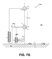
- polyphase waveguide probe 200 i shown is yet another example of the polyphase waveguide probe 200 ( FIG. 6 ), denoted herein as polyphase waveguide probe 200 i , according to one embodiment.
- the polyphase waveguide probe 200 i is very similar to the polyphase waveguide probe 200 h ( FIG. 7H ) except for the fact that the excitation source 213 is series-coupled to the probe coupling circuit 209 i as will be described.
- the polyphase waveguide probe 200 i includes the charge terminals T 1 and T 2 that are positioned along a vertical axis z that is substantially normal to the plane presented by the lossy conducting medium 203 .
- the second medium 206 is above the lossy conducting medium 203 .
- the charge terminal T 1 has a self-capacitance C 1
- the charge terminal T 2 has a self-capacitance C 2 .
- charges Q 1 and Q 2 are imposed on the charge terminals T 1 and T 2 , respectively, depending on the voltages applied to the charge terminals T 1 and T 2 at any given instant.
- a mutual capacitance C M may exist between the charge terminals T 1 and T 2 depending on the distance there between.
- bound capacitances may exist between the respective charge terminals T 1 and T 2 and the lossy conducting medium 203 depending on the heights of the respective charge terminals T 1 and T 2 with respect to the lossy conducting medium 203 .
- the polyphase waveguide probe 200 i also includes a probe coupling circuit 209 i comprising a first coil L 1i and a second coil L 2i .
- the first lead of the first coil L 1i is coupled to the charge terminal T 1
- the second lead of the first coil L 1i is coupled to the second charge terminal T 2 .
- a first lead of the second coil L 2i is coupled to a terminal T T
- the second lead of the second coil L 2i is coupled to an output of the excitation source 213 .
- a ground lead of the excitation source 213 is coupled to the lossy conducting medium 203 .
- the terminal T T is positioned relative to the charge terminal T 2 such that a coupling capacitance C C exists between the charge terminal T 2 and the terminal T T .
- the polyphase waveguide probe 200 i provides one example where the excitation source 213 is series-coupled to the probe coupling circuit 209 i as mentioned above. Specifically, the excitation source 213 is coupled between the coil L 2i and the lossy conducting medium 203 .
- the heights of the respective charge terminals T 1 and T 2 may be altered with respect to the lossy conducting medium 203 and with respect to each other. Also, the sizes of the charge terminals T 1 and T 2 may be altered. In addition, the size of each of the coils L 1i and L 2i may be altered by adding or eliminating turns or by changing some other dimension of the respective coils L 1i or L 2i . Also the spacing between the charge terminal T 2 and the terminal T T may be altered, thereby modifying the coupling capacitance C C as can be appreciated.
- the polyphase waveguide probe 200 j includes the charge terminals T 1 and T 2 that are positioned along a vertical axis z that is substantially normal to the plane presented by the lossy conducting medium 203 .
- the second medium 206 is above the lossy conducting medium 203 .
- the charge terminal T 1 comprises a sphere and the charge terminal T 2 comprises a disk.
- the polyphase waveguide probe 200 j provides an illustration that the charge terminals T N may comprise any shape.
- the charge terminal T 1 has a self-capacitance C 1
- the charge terminal T 2 has a self-capacitance C 2 .
- charges Q 1 and Q 2 are imposed on the charge terminals T 1 and T 2 , respectively, depending on the voltages applied to the charge terminals T 1 and T 2 at any given instant.
- a mutual capacitance C M may exist between the charge terminals T 1 and T 2 depending on the distance there between.
- bound capacitances may exist between the respective charge terminals T 1 and T 2 and the lossy conducting medium 203 depending on the heights of the respective charge terminals T 1 and T 2 with respect to the lossy conducting medium 203 .
- the polyphase waveguide probe 200 j includes a probe coupling circuit 209 j comprising an inductive impedance comprising a coil L 1j having a pair of leads that are coupled to respective ones of the charge terminals T 1 and T 2 .
- the coil L 1j is specified to have an electrical length that is one-half (1 ⁇ 2) of the wavelength at the operating frequency of the polyphase waveguide probe 200 j . While the electrical length of the coil L 1j is specified as approximately one-half (1 ⁇ 2) the wavelength at the operating frequency, it is understood that the coil L 1j may be specified with an electrical length at other values as was discussed with reference to the polyphase waveguide probe 200 a ( FIG. 7A ) described above.
- the probe coupling circuit 209 j includes a tap 223 on the coil L 1j that is coupled to the lossy conducting medium 203 .
- the excitation source 213 is magnetically coupled to the probe coupling circuit 209 j in a manner similar as was mentioned with respect to the polyphase waveguide probe 200 a ( FIG. 7A ) set forth above. To this end, the excitation source 213 is coupled to a coil L P that acts as a primary and the coil L 1j acts as a secondary.
- the coil L P can be positioned at any location along the coil L 1j . Also, the coil L P can be positioned above or below the tap 223 .
- the heights of the respective charge terminals T 1 and T 2 may be altered with respect to the lossy conducting medium 203 and with respect to each other. Also, the sizes of the charge terminals T 1 and T 2 may be altered. In addition, the size of the coil L 1j may be altered by adding or eliminating turns or by changing some other dimension of the coil L 1j . Further, the position of the tap 223 on the coil L 1j may be adjusted.
- each of the polyphase waveguide probes 200 a - j may be excited to transmit energy conveyed in the form of a guided wave, or waveguide mode along the surface of the lossy conducting medium 203 .
- the elements of each of the polyphase waveguide probes 200 a - j may be adjusted to impose a desired voltage magnitude and phase on the respective charge terminals T 1 and T 2 when the respective polyphase waveguide probe 200 a - j is excited.
- excitation may occur by applying energy from an excitation source 213 to the respective polyphase waveguide probe 200 a - j as was described above.
- the voltage magnitudes and phases imposed on the charge terminals T 1 and T 2 may be adjusted in order to substantially synthesize the fields that are substantially mode-matched to the guided or Zenneck surface-waveguide mode of the lossy conducting medium 203 at the site of transmission given the local permittivity ⁇ r , conductivity a, and potentially other parameters of the lossy conducting medium 203 .
- the waveguide mode of the surface-guided wave is expressed in Equations (21), (22), and (23) set forth above. This surface-waveguide mode has a radial surface current density expressed in Equation (20) in Amperes per meter.
- a guided surface wave may be launched if such fields at least approximate the surface-waveguide mode.
- the fields are synthesized to match the surface-waveguide mode within an acceptable engineering tolerance so as to launch a guided surface wave.
- the polyphase waveguide probes 200 may be adjusted to match the radial surface current density of the guided surface-waveguide mode within an acceptable engineering tolerance so as to launch a Zenneck surface wave mode.
- the various polyphase waveguide probes 200 a - j set forth above excite surface currents, the fields of which are designed to approximately match a propagating Zenneck surface wave mode and a Zenneck surface wave is launched.
- the guiding interface is the interface between Region 1 ( FIG. 2 ) and Region 2 ( FIG. 2 ) as described above.
- the guiding interface is the interface between the lossy conducting medium 203 presented by the Earth and the atmospheric medium as described above.
- FIGS. 8A, 8B, and 8C shown are examples of graphs 300 a , 300 b , and 300 c that depict field strength in Volts per meter as a function of distance in kilometers for purposes of comparison between a Zenneck surface wave and conventionally radiated fields.
- the various graphs 300 a , 300 b , and 300 c illustrate how the distance of transmission of a Zenneck surface wave varies with the frequency of transmission.
- Each graph 300 a , 300 b , and 300 c depicts a corresponding guided field strength curve 303 a , 303 b , and 303 c and corresponding radiated field strength curves 306 a , 306 b , and 306 c .
- the guided field strength curves 303 a , 303 b , and 303 c were generated assuming various parameters. Specifically, the graphs 300 a , 300 b , and 300 c were calculated with a constant charge Q 1 ( FIG. 3 ) applied to the upper terminal T 1 ( FIG. 3 ) at frequencies of 10 MHz, 1 MHz, and 0.1 MHz, respectively.
- the resulting terminal charge Q T1 which is the controlling parameter for field strength was kept at the same value for all three guided field strength curve 303 a , 303 b , and 303 c.
- the Zenneck surface wave for each case is identified as guided field strength curves 303 a , 303 b , and 303 c , respectively.
- the Norton ground wave field strength in Volts per meter for a short vertical monopole antenna, of the same height as the respective polyphase waveguide probe 200 , with an assumed ground loss of 10 ohms, is represented by the radiated field strength curves 306 a , 306 b , and 306 c , respectively. It is asserted that this is a reasonably realistic assumption for monopole antenna structures operating at these frequencies.
- the critical point is that a properly mode-matched polyphase waveguide probe launches a guided surface wave which dramatically outperforms the radiation field of any monopole at distances out to just beyond the “knee” in the guided field strength curves 303 a - c of the respective Zenneck surface waves.
- the propagation distance of a guided surface wave varies as a function of the frequency of transmission. Specifically, the lower the transmission frequency, the less the exponential attenuation of the guided surface wave and, therefore, the farther the guided surface wave will propagate. As mentioned above, the field strength of a guided surface wave falls off at a rate of
- each of the guided field strength curves 303 a , 303 b , and 303 c feature a knee as was described above. As the frequency of transmission of a polyphase waveguide probe described herein decreases, the knee of the corresponding guided field strength curve 303 a , 303 b , and 303 c will push to the right in the graph.
- FIG. 8A shows a guided field strength curve 303 a and a radiated field strength curve 306 a generated at a frequency of 10 Megahertz.
- the guided surface wave falls off below 10 kilometers.
- the guided field strength curve 303 b and the radiated field strength curve 306 b are generated at a frequency of 1 Megahertz.
- the guided field strength curve 303 b falls off at approximately 100 kilometers.
- the guided field strength curve 303 c and the radiated field strength curve 306 c are generated at a frequency of 100 Kilohertz (which is 0.1 Megahertz).
- the guided field strength curve 303 c falls off at between 4000-7000 Kilometers.
- the frequency is low enough, it may be possible to transmit a guided surface wave around the entire Earth. It is believed that such frequencies may be at or below approximately 20-25 kilohertz. It should be noted that at such low frequencies, the lossy conducting medium 203 ( FIG. 6 ) ceases to be a plane and becomes a sphere. Thus, when a lossy conducting medium 203 comprises a terrestrial medium, the calculation of guided field strength curves will be altered to take into account the spherical shape at low frequencies where the propagation distances approach size of the terrestrial medium.
- a polyphase waveguide probe 200 ( FIG. 6 ) using the terrestrial medium of Earth as the lossy conducting medium 203 according to the various embodiments.
- the frequency of operation and identify the desired field strength of the guided surface wave at a distance of interest from the respective polyphase waveguide probe 200 to be constructed.
- To determine the charge Q 1 needed one would need to obtain the permittivity ⁇ r and the conductivity a of the Earth at the transmission site. These values can be obtained by measurement or by reference to conductivity charts published, for example, by the Federal Communications Commission or the Committee Consultif International Radio (CCIR).
- the permittivity ⁇ r , conductivity ⁇ , and the desired field strength at the specified distance are known, the needed charge Q 1 can be determined by direct calculation of the field strength from Zenneck's exact expressions set forth in Equations (21)-(23) above.
- the bandwidth of the polyphase waveguide probes 200 described herein is relatively large. This results in a significant degree of flexibility in specifying the self-capacitance C 1 or the voltage V as described above. However, it should be understood that as the self-capacitance C 1 is reduced and the voltage V increased, the bandwidth of the resulting polyphase waveguide probe 200 will diminish.
- a smaller self-capacitance C 1 may make a given polyphase waveguide probe 200 more sensitive to small variations in the permittivity ⁇ r or conductivity ⁇ of the Earth at or near the transmission site.
- Such variation in the permittivity ⁇ r or conductivity ⁇ might occur due to variation in the climate given the transition between the seasons or due to changes in local weather conditions such as the onset of rain, drought, and/or other changes in local weather. Consequently, according to one embodiment, the charge terminal T 1 may be specified so as to have a relatively large self-capacitance C 1 as is practicable.
- the self-capacitance C 1 of the charge terminal T 1 and the voltage to be imposed thereon are determined, next the self-capacitance C 2 and physical location of the second charge terminal T 2 are to be determined.
- the self-capacitance C 2 of the charge terminal T 2 it has been found easiest to specify the self-capacitance C 2 of the charge terminal T 2 to be the same as the self-capacitance C 1 of the charge terminal T 1 . This may be accomplished by making the size and shape of the charge terminal T 2 the same as the size and shape of the charge terminal T 1 . This would ensure that symmetry is maintained and will avoid the possibility of unusual phase shifts between the two charge terminals T 1 and T 2 that might negatively affect achieving a match with the complex Brewster angle as described above.
- the self-capacitances C 1 and C 2 are the same for both charge terminals T 1 and T 2 will result in the same voltage magnitudes on the charge terminals T 1 and T 2 .
- the self-capacitances C 1 and C 2 may differ, and the shape and size of the charge terminals T 1 and T 2 may differ.
- the charge terminal T 2 may be positioned directly under the charge terminal T 1 along the vertical axis z ( FIG. 6 ) as described above. Alternatively, it may be possible to position the charge terminal T 2 at some other location with some resulting effect.
- the distance between the charge terminals T 1 and T 2 should be specified so as to provide for the best match between the fields generated by the polyphase waveguide probe 200 and the guided surface-waveguide mode at the site of transmission. As a suggested starting point, this distance may be set so that the mutual capacitance C M ( FIG. 6 ) between the charge terminals T 1 and T 2 is the same or less than the isolated capacitance C 1 on the charge terminal T 1 . Ultimately, one should specify the distance between the charge terminals T 1 and T 2 to make the mutual capacitance C M as small as is practicable. The mutual capacitance C M may be determined by measurement, and the charge terminals T 1 and T 2 may be positioned accordingly.
- the so-called “image complex-depth” phenomenon comes into bearing here. This would entail consideration of the superposed fields on the surface of the Earth from the charge reservoirs T 1 and T 2 that have charges Q 1 and Q 2 , and from the subsurface images of the charges Q 1 and Q 2 as height h is varied.
- a practical starting point is a height h at which the bound capacitance of each of the charge reservoirs T 1 and T 2 with respect to the ground is negligible such that the capacitance associated with the charge terminals T 1 and T 2 is essentially their isolated self-capacitance C 1 and C 2 , respectively.
- Another consideration to take into account when determining the height h associated with a polyphase waveguide probe 200 is whether radiation is to be avoided. Specifically, as the height h of the polyphase waveguide probe 200 approaches an appreciable portion of a wavelength at the frequency of operation, the radiation resistance R r will grow quadratically with height h and radiation will begin to dominate over the generation of a guided surface wave as described above.
- One benchmark set forth above that ensures the Zenneck surface wave will dominate over any radiation is to make sure the height h is less than 10% of the wavelength at the frequency of operation, although other benchmarks may be specified. In some cases, it may be desired to allow some degree of radiation to occur in addition to launching a guided surface wave, where the height h may be specified accordingly.
- the probe coupling circuit 209 ( FIG. 6 ) is specified to provide for the voltage phase between the charge terminals T 1 and T 2 .
- the voltage phase appears to have a significant effect on creating fields that mode-match the guided surface-waveguide mode at the site of transmission.
- the probe coupling circuit 209 may be specified to provide for a voltage phase differential of 180 degrees on the charge terminals T 1 and T 2 . That is to say, the probe coupling circuit 209 is specified so that voltage V on the charge terminal T 1 is 180 degrees out of phase with respect to the voltage on the charge terminal T 2 .
- one example approach is to place a coil L 1a ( FIG. 7A ) between the charge terminals T 1 and T 2 as described above with reference to the polyphase waveguide probe 200 a and adjust the coil L 1a until the resulting system is electrically half-wave resonant. This would place a voltage V on the charge terminal T 1 and voltage ⁇ V on the charge terminal T 2 such that the largest voltages are placed on the charge terminals T 1 and T 2 180 degrees out of phase.
- the excitation source 213 may then be coupled to the probe coupling circuit 209 and the output voltage adjusted to achieve the required voltage V to provide for the needed charge Q 1 as described above.
- the excitation source 213 may be coupled via magnetic coupling, capacitive coupling, or conductive coupling (direct) to the probe coupling circuit 209 .
- the output of the excitation source 213 may be stepped up using a transformer or via some other approach if necessary.
- the location of the coil L 1a can be at any location such as down on the ground by the excitation source 213 .
- the coil L 1a can be positioned directly between the charge reservoirs T 1 and T 2 . Principles of impedance matching may be applied when coupling the excitation source 213 to the probe coupling circuit 209 .
- phase differential does not necessarily have to be 180 degrees.
- FIG. 9 shown is a graph that presents the measured field strength of an electromagnetic field transmitted by one embodiment of an experimental polyphase waveguide probe measured on Oct. 14, 2012 in Madison, N.H.
- the frequency of transmission was 59 MHz with a voltage of 60 mV imposed on the charge terminal T 1 of the experimental polyphase waveguide probe.
- the self-capacitance C 1 of the experimental polyphase waveguide probe was 8.5 pF.
- the conductivity ⁇ of the ground at the test site is 0.0002 mhos/m, and the permittivity ⁇ r of the ground at the test site was 5. These values were measured in situ at the frequency in use.
- the graph includes a guided field strength curve 400 that is labeled a “Zenneck” curve at 80% efficiency and a radiated field strength curve 403 that is labeled a “Norton” curve at 100% radiation efficiency, which is the best possible.
- the radiated field strength curve 403 represents the radiated electromagnetic fields that would be generated by a 1 ⁇ 4 wavelength monopole antenna operating at a frequency of 59 MHz.
- the circles 406 on the graph represent measured field strengths produced by the experimental polyphase waveguide probe. The field strength measurements were performed with a NIST-traceable Potomac Instruments FIM-71 commercial VHF field strength meter. As can be seen, the measured field strengths fall along the theoretical guided field strength curve 400 . These measured field strengths are consistent with the propagation of a guided or Zenneck surface wave.
- the curve J(r) indicates the phase of the fields incident to the currents J 1 and J 2 with a transition between the currents J 1 and J 2 as shown.
- the curve 503 indicates the asymptote depicting the phase of the current J 1
- the curve 506 indicates the asymptote depicting the phase of the current J 2 .
- a difference of approximately 45 degrees generally exists between the phases of the respective currents J 1 and J 2 .
- the circles 509 indicate measurements of the phase of the current J(r) generated by the experimental polyphase waveguide probe operating at 59 MHz as with FIG. 9 .
- the circles 509 fall along the curve J(r) indicating that there is a transition of the phase of the current J(r) from the curve 503 to the curve 506 .
- these phase measurements are consistent with the phase with the presence of a guided or Zenneck surface wave.
- FIG. 11 shown is a graph of a second set of measured data that depicts the field strength of an electromagnetic field transmitted by a second embodiment of an experimental polyphase waveguide probe measured on Nov. 1, 2003 in the vicinity of Ashland, N.H. and across the region north of Lake Winnipesaukee.
- the frequency of transmission was 1850 kHz with a voltage of 1250 V imposed on the charge terminal T 1 of the experimental polyphase waveguide probe.
- the self-capacitance C 1 of the experimental polyphase waveguide probe in this experiment which was a flat conducting disk of 1 meter radius, was measured to be 70 pF.
- the polyphase waveguide probe was arranged as illustrated in FIG.
- the radiated field strength curve 603 represents the conventional Norton ground wave field radiated from a conventional stub monopole antenna operating at a frequency of 1850 kHz over the lossy Earth.
- the circles 606 on the graph represent measured field strengths produced by the experimental polyphase waveguide probe.
- the measured field strengths fall closely along the theoretical Zenneck guided field strength curve 600 .
- the field strength measurements were performed with a NIST-traceable Potomac Instruments FIM-41 MF/HF field strength meter.
- the measured field strength data are consistent with the presence of a guided or Zenneck surface wave. It is apparent from the experimental data that the measured field strengths observed at distances less than 15 miles could not possibly be due to conventional Norton ground wave propagation, and can only be due to guided surface wave propagation launched by the polyphase probe operating as disclosed above. Under the given 1.85 MHz experimental conditions, out at 20 miles it appears that a Norton ground wave component has finally overtaken the Zenneck surface wave component.
- a comparison of the measured Zenneck surface wave data shown in FIG. 9 at 59 MHz with the measured data in FIG. 11 at 1.85 MHz illustrates the great advantage of employing a polyphase waveguide probe according to the various embodiments at lower frequencies.
- FIGS. 12A, 12B, and 13 shown are examples of generalized receive circuits for using the surface-guided waves in wireless power delivery systems.
- FIGS. 12A and 12B include a linear probe 703 and a tuned resonator 706 .
- FIG. 13 is a magnetic coil 709 according to various embodiments of the present disclosure.
- each one of the linear probe 703 , the tuned resonator 706 , and the magnetic coil 709 may be employed to receive power transmitted in the form of a guided surface wave on the surface of a lossy conducting medium 203 ( FIG. 6 ) according to various embodiments.
- the lossy conducting medium 203 comprises a terrestrial medium.
- the open-circuit terminal voltage at the output terminals 713 of the linear probe 703 depends upon the effective height of the linear probe 703 .
- An electrical load 716 is coupled to the output terminals 713 through an impedance matching network 719 .
- the electrical load 716 should be substantially impedance matched to the linear probe 703 as will be described below.
- the tuned resonator 706 includes a charge terminal T R that is elevated above the lossy conducting medium 203 .
- the charge terminal T R has a self-capacitance C R .
- the bound capacitance should preferably be minimized as much as is practicable, although this may not be entirely necessary in every instance of a polyphase waveguide probe 200 .
- the tuned resonator 706 also includes a coil L R .
- One end of the coil L R is coupled to the charge terminal T R
- the other end of the coil L R is coupled to the lossy conducting medium 203 .
- the tuned resonator 706 (which may also be referred to as tuned resonator L R -C R ) comprises a series-tuned resonator as the charge terminal C R and the coil L R are situated in series.
- the tuned resonator 706 is tuned by adjusting the size and/or height of the charge terminal T R , and/or adjusting the size of the coil L R so that the reactive impedance of the structure is substantially eliminated.
- the reactance presented by the self-capacitance C R is calculated as
- the total capacitance of the tuned resonator 706 may also include capacitance between the charge terminal T R and the lossy conducting medium 203 , where the total capacitance of the tuned resonator 706 may be calculated from both the self-capacitance C R and any bound capacitance as can be appreciated.
- the charge terminal T R may be raised to a height so as to substantially reduce or eliminate any bound capacitance. The existence of a bound capacitance may be determined from capacitance measurements between the charge terminal T R and the lossy conducting medium 203 .
- the inductive reactance presented by a discrete-element coil L R may be calculated as j ⁇ L, where L is the lumped-element inductance of the coil L R . If the coil L R is a distributed element, its equivalent terminal-point inductive reactance may be determined by conventional approaches. To tune the tuned resonator 706 , one would make adjustments so that the inductive reactance presented by the coil L R equals the capacitive reactance presented by the tuned resonator 706 so that the resulting net reactance of the tuned resonator 706 is substantially zero at the frequency of operation.
- An impedance matching network 723 may be inserted between the probe terminals 721 and the electrical load 726 in order to effect a conjugate-match condition for maxim power transfer to the electrical load 726 .
- an electrical load 726 may be coupled to the tuned resonator 706 by way of magnetic coupling, capacitive coupling, or conductive (direct tap) coupling.
- the elements of the coupling network may be lumped components or distributed elements as can be appreciated. In the embodiment shown in FIG.
- magnetic coupling is employed where a coil L S is positioned as a secondary relative to the coil L R that acts as a transformer primary.
- the coil L S may be link coupled to the coil L R by geometrically winding it around the same core structure and adjusting the coupled magnetic flux as can be appreciated.
- the tuned resonator 706 comprises a series-tuned resonator, a parallel-tuned resonator or even a distributed-element resonator may also be used.
- the magnetic coil 709 comprises a receive circuit that is coupled through an impedance coupling network 733 to an electrical load 736 .
- the magnetic coil 709 may be positioned so that the magnetic flux of the guided surface wave, H ⁇ , passes through the magnetic coil 709 , thereby inducing a current in the magnetic coil 709 and producing a terminal point voltage at its output terminals 729 .
- ⁇ is the coupled magnetic flux
- ⁇ r is the effective relative permeability of the core of the magnetic coil 709
- ⁇ o is the permeability of free space
- H is the incident magnetic field strength vector
- n is a unit vector normal to the cross-sectional area of the turns
- a CS is the area enclosed by each loop.
- the magnetic coil 709 may be tuned to the guided wave frequency either as a distributed resonator or with an external capacitor across its output terminals 729 , as the case may be, and then impedance-matched to an external electrical load 736 through a conjugate impedance matching network 733 .
- the current induced in the magnetic coil 709 may be employed to optimally power the electrical load 736 .
- the receive circuit presented by the magnetic coil 709 provides an advantage in that it does not have to be physically connected to the ground.
- the receive circuits presented by the linear probe 703 , the tuned resonator 706 , and the magnetic coil 709 each facilitate receiving electrical power transmitted from any one of the embodiments of polyphase waveguide probes 200 described above.
- the energy received may be used to supply power to an electrical load 716 / 726 / 736 via a conjugate matching network as can be appreciated.
- the receive circuits presented by the linear probe 703 , the tuned resonator 706 , and the magnetic coil 709 will load the excitation source 213 ( FIG. 3 ) that is applied to the polyphase waveguide probe 200 , thereby generating the guided surface wave to which such receive circuits are subjected.
- the guided surface wave generated by a given polyphase waveguide probe 200 described above comprises a transmission line mode.
- a power source that drives a radiating antenna that generates a radiated electromagnetic wave is not loaded by the receivers, regardless of the number of receivers employed.
- a given polyphase waveguide probe 200 and receive circuits in the form of the linear probe 703 , the tuned resonator 706 , and/or the magnetic coil 709 can together make up a wireless distribution system.
- the distance of transmission of a guided surface wave using a polyphase waveguide probe 200 as set forth above depends upon the frequency, it is possible that wireless power distribution can be achieved across wide areas and even globally.
- the conventional wireless-power transmission/distribution systems extensively investigated today include “energy harvesting” from radiation fields and also sensor coupling to inductive or reactive near-fields.
- the present wireless-power system does not waste power in the form of radiation which, if not intercepted, is lost forever.
- the presently disclosed wireless-power system limited to extremely short ranges as with conventional mutual-reactance coupled near-field systems.
- the wireless-power system disclosed herein probe-couples to the novel surface-guided transmission line mode, which is equivalent to delivering power to a load by a wave-guide or a load directly wired to the distant power generator.
- FIG. 14A shown is a schematic that represents the linear probe 703 and the tuned resonator 706 .
- FIG. 14B shows a schematic that represents the magnetic coil 709 .
- the linear probe 703 and the tuned resonator 706 may each be considered a Thevenin equivalent represented by an open-circuit terminal voltage source V S and a dead network terminal point impedance Z S .
- the magnetic coil 709 may be viewed as a Norton equivalent represented by a short-circuit terminal current source I S and a dead network terminal point impedance Z S .
- Each electrical load 716 / 726 / 736 ( FIGS. 12A-B and FIG. 13 ) may be represented by a load impedance Z L .
- the electrical load 716 / 726 / 736 is impedance matched to each receive circuit, respectively.
- the conjugate match which states that if, in a cascaded network, a conjugate match occurs at any terminal pair then it will occur at all terminal pairs, then asserts that the actual electrical load 716 / 726 / 736 will also see a conjugate match to its impedance, Z L ′. See Everitt, W. L. and G. E. Tanner, Communication Engineering , McGraw-Hill, 3 rd edition, 1956, p. 407. This ensures that the respective electrical load 716 / 726 / 736 is impedance matched to the respective receive circuit and that maximum power transfer is established to the respective electrical load 716 / 726 / 736 .
Abstract
Disclosed are various embodiments systems and methods for transmission and reception of electrical energy along a surface of a terrestrial medium. A polyphase waveguide probe that transmits electrical energy in the form of a guided surface wave along a surface of a terrestrial medium. A receive circuit is used to receive the electrical energy.
Description
This application is related to co-pending U.S. patent application Ser. No. 13/789,538 filed on Mar. 7, 2013 and entitled “EXCITATION AND USE OF GUIDED SURFACE WAVE MODES ON LOSSY MEDIA.”
For over a century, signals transmitted by radio waves involved radiation fields launched using conventional antenna structures. In contrast to radio science, electrical power distribution systems in the last century involved the transmission of energy guided along electrical conductors. This understanding of the distinction between radio frequency (RF) and power transmission has existed since the early 1900's.
Many aspects of the present disclosure can be better understood with reference to the following drawings. The components in the drawings are not necessarily to scale, emphasis instead being placed upon clearly illustrating the principles of the disclosure. Moreover, in the drawings, like reference numerals designate corresponding parts throughout the several views.
Referring to FIG. 1 , to begin, some terminology shall be established to provide clarity in the discussion of concepts to follow. First, as contemplated herein, a formal distinction is drawn between radiated electromagnetic fields and guided electromagnetic fields.
As contemplated herein, a radiated electromagnetic field comprises electromagnetic energy that is emitted from a source structure in the form of waves that are not bound to a waveguide. For example, a radiated electromagnetic field is generally a field that leaves an electric structure such as an antenna and propagates through the atmosphere or other medium and is not bound to any waveguide structure. Once radiated electromagnetic waves leave an electric structure such as an antenna, they continue to propagate in the medium of propagation (such as air) independent of their source until they dissipate regardless of whether the source continues to operate. Once electromagnetic waves are radiated, they are not recoverable unless intercepted, and, if not intercepted, the energy inherent in radiated electromagnetic waves is lost forever. Electrical structures such as antennas are designed to radiate electromagnetic fields by maximizing the ratio of the radiation resistance to the structure loss resistance. Radiated energy spreads out in space and is lost regardless of whether a receiver is present. The energy density of radiated fields is a function of distance due to geometrical spreading. Accordingly, the term “radiate” in all its forms as used herein refers to this form of electromagnetic propagation.
A guided electromagnetic field is a propagating electromagnetic wave whose energy is concentrated within or near boundaries between media having different electromagnetic properties. In this sense, a guided electromagnetic field is one that is bound to a waveguide and may be characterized as being conveyed by the current flowing in the waveguide. If there is no load to receive and/or dissipate the energy conveyed in a guided electromagnetic wave, then no energy is lost except for that dissipated in the conductivity of the guiding medium. Stated another way, if there is no load for a guided electromagnetic wave, then no energy is consumed. Thus, a generator or other source generating a guided electromagnetic field does not deliver real power unless a resistive load is present. To this end, such a generator or other source essentially runs idle until a load is presented. This is akin to running a generator to generate a 60 Hertz electromagnetic wave that is transmitted over power lines where there is no electrical load. It should be noted that a guided electromagnetic field or wave is the equivalent to what is termed a “transmission line mode.” This contrasts with radiated electromagnetic waves in which real power is supplied at all times in order to generate radiated waves. Unlike radiated electromagnetic waves, guided electromagnetic energy does not continue to propagate along a finite length waveguide after the energy source is turned off. Accordingly, the term “guide” in all its forms as used herein refers to this transmission mode of electromagnetic propagation.
To further illustrate the distinction between radiated and guided electromagnetic fields, reference is made to FIG. 1 that depicts graph 100 of field strength in decibels (dB) above an arbitrary reference in volts per meter as a function of distance in kilometers on a log-dB plot. The graph 100 of FIG. 1 depicts a guided field strength curve 103 that shows the field strength of a guided electromagnetic field as a function of distance. This guided field strength curve 103 is essentially the same as a transmission line mode. Also, the graph 100 of FIG. 1 depicts a radiated field strength curve 106 that shows the field strength of a radiated electromagnetic field as a function of distance.
Of interest are the shapes of the curves 103/106 for radiation and for guided wave propagation. The radiated field strength curve 106 falls off geometrically (1/d, where d is distance) and is a straight line on the log-log scale. The guided field strength curve 103, on the other hand, has the characteristic exponential decay of e−αd/√{square root over (d)} and exhibits a distinctive knee 109. Thus, as shown, the field strength of a guided electromagnetic field falls off at a rate of e−αd/√{square root over (d)}, whereas the field strength of a radiated electromagnetic field falls off at a rate of 1/d, where d is the distance. Due to the fact that the guided field strength curve 103 falls off exponentially, the guided field strength curve 103 features the knee 109 as mentioned above. The guided field strength curve 103 and the radiated field strength curve 106 intersect at a crossover point 113 which occurs at a crossover distance. At distances less than the crossover distance, the field strength of a guided electromagnetic field is significantly greater at most locations than the field strength of a radiated electromagnetic field. At distances greater than the crossover distance, the opposite is true. Thus, the guided and radiated field strength curves 103 and 106 further illustrate the fundamental propagation difference between guided and radiated electromagnetic fields. For an informal discussion of the difference between guided and radiated electromagnetic fields, reference is made to Milligan, T., Modern Antenna Design, McGraw-Hill, 1st Edition, 1985, pp. 8-9, which is incorporated herein by reference in its entirety.
The distinction between radiated and guided electromagnetic waves, made above, is readily expressed formally and placed on a rigorous basis. That two such diverse solutions could emerge from one and the same linear partial differential equation, the wave equation, analytically follows from the boundary conditions imposed on the problem. The Green function for the wave equation, itself, contains the distinction between the nature of radiation and guided waves.
In empty space, the wave equation is a differential operator whose eigenfunctions possess a continuous spectrum of eigenvalues on the complex wave-number plane. This transverse electro-magnetic (TEM) field is called the radiation field, and those propagating fields are called “Hertzian waves”. However, in the presence of a conducting boundary, the wave equation plus boundary conditions mathematically lead to a spectral representation of wave-numbers composed of a continuous spectrum plus a sum of discrete spectra. To this end, reference is made to Sommerfeld, A., “Uber die Ausbreitung der Wellen in der Drahtlosen Telegraphie,” Annalen der Physik, Vol. 28, 1909, pp. 665-736. Also see Sommerfeld, A., “Problems of Radio,” published as Chapter 6 in Partial Differential Equations in Physics—Lectures on Theoretical Physics: Volume VI, Academic Press, 1949, pp. 236-289, 295-296; Collin, R. E., “Hertzian Dipole Radiating Over a Lossy Earth or Sea: Some Early and Late 20th Century Controversies,” IEEE Antennas and Propagation Magazine, Vol. 46, No. 2, April 2004, pp. 64-79; and Reich, H. J., Ordnung, P. F, Krauss, H. L., and Skalnik, J. G., Microwave Theory and Techniques, Van Nostrand, 1953, pp. 291-293, each of these references being incorporated herein by reference in their entirety.
To summarize the above, first, the continuous part of the wave-number eigenvalue spectrum, corresponding to branch-cut integrals, produces the radiation field, and second, the discrete spectra, and corresponding residue sum arising from the poles enclosed by the contour of integration, result in non-TEM traveling surface waves that are exponentially damped in the direction transverse to the propagation. Such surface waves are guided transmission line modes. For further explanation, reference is made to Friedman, B., Principles and Techniques of Applied Mathematics, Wiley, 1956, pp. pp. 214, 283-286, 290, 298-300.
In free space, antennas excite the continuum eigenvalues of the wave equation, which is a radiation field, where the outwardly propagating RF energy with Ez and Hφ in-phase is lost forever. On the other hand, waveguide probes excite discrete eigenvalues, which results in transmission line propagation. See Collin, R. E., Field Theory of Guided Waves, McGraw-Hill, 1960, pp. 453, 474-477. While such theoretical analyses have held out the hypothetical possibility of launching open surface guided waves over planar or spherical surfaces of lossy, homogeneous media, for more than a century no known structures in the engineering arts have existed for accomplishing this with any practical efficiency. Unfortunately, since it emerged in the early 1900's, the theoretical analysis set forth above has essentially remained a theory and there have been no known structures for practically accomplishing the launching of open surface guided waves over planar or spherical surfaces of lossy, homogeneous media.
According to the various embodiments of the present disclosure, various polyphase waveguide probes are described that are configured to excite radial surface currents having resultant fields that synthesize the form of surface-waveguide modes along the surface of a lossy conducting medium. Such guided electromagnetic fields are substantially mode-matched in magnitude and phase to a guided surface wave mode on the surface of the lossy conducting medium. Such a guided surface wave mode may also be termed a Zenneck surface wave mode. By virtue of the fact that the resultant fields excited by the polyphase waveguide probes described herein are substantially mode-matched to a Zenneck surface wave mode on the surface of the lossy conducting medium, a guided electromagnetic field in the form of a Zenneck surface wave is launched along the surface of the lossy conducting medium. According to one embodiment, the lossy conducting medium comprises a terrestrial medium such as the Earth.
Referring to FIG. 2 , shown is a propagation interface that provides for an examination of the boundary value solution to Maxwell's equations derived in 1907 by Jonathan Zenneck as set forth in his paper Zenneck, J., “On the Propagation of Plane Electromagnetic Waves Along a Flat Conducting Surface and their Relation to Wireless Telegraphy,” Annalen der Physik, Serial 4, Vol. 23, Sep. 20, 1907, pp. 846-866. FIG. 2 depicts cylindrical coordinates for radially propagating waves along the interface between a lossy conducting medium specified as Region 1 and an insulator specified as Region 2. Region 1 may comprise, for example, any lossy conducting medium. In one example, such a lossy conducting medium may comprise a terrestrial medium such as the Earth or other medium. Region 2 is a second medium that shares a boundary interface with Region 1 and has different constitutive parameters relative to Region 1. Region 2 may comprise, for example, any insulator such as the atmosphere or other medium. The reflection coefficient for such a boundary interface goes to zero only for incidence at a complex Brewster angle. See Stratton, J. A., Electromagnetic Theory, McGraw-Hill, 1941, p. 516.
According to various embodiments, the present disclosure sets forth various polyphase waveguide probes that generate electromagnetic fields that are substantially mode-matched to a Zenneck surface wave mode on the surface of the lossy conducting medium comprising Region 1. According to various embodiments, such electromagnetic fields substantially synthesize a wave front incident at a complex Brewster angle of the lossy conducting medium that results in zero reflection.
To explain further, in Region 2, where ejωt field variation is assumed and where ρ≠0 and z≧0 (z is a vertical coordinate normal to the surface of Region 1, ρ is the radial dimension in cylindrical coordinates), Zenneck's closed-form exact solution of Maxwell's equations satisfying the boundary conditions along the interface are expressed by the following electric field and magnetic field components:
In Region 1, where ejωt field variation is assumed and where ρ≠0 and z≦0, Zenneck's closed-form exact solution of Maxwell's equations satisfying the boundary conditions along the interface are expressed by the following electric field and magnetic field components:
In these expressions, Hn (2)(−jγρ) is a complex argument Hankel function of the second kind and order n, u1 is the propagation constant in the positive vertical direction in
The propagation constants in the ±z directions are determined by separating the wave equation above and below the interface between Regions 1 and 2, and imposing the boundary conditions. This exercise gives, in Region 2,
and gives, in
u 1 =−u 2(∈r −jx). (8)
The radial propagation constant γ is given by
γ=j√{square root over (k o 2 +u 2 2)}, (9)
which is a complex expression. In all of the above Equations,
where μo comprises the permeability of free space, ∈r comprises relative permittivity of
Thus, Equations (1)-(3) may be considered to be a cylindrically-symmetric, radially-propagating waveguide mode. See Barlow, H. M., and Brown, J., Radio Surface Waves, Oxford University Press, 1962, pp. 10-12, 29-33. The present disclosure details structures that excite this “open boundary” waveguide mode. Specifically, according to various embodiments, a polyphase waveguide probe is provided with charge terminals of appropriate size that are positioned relative to each other and are fed with voltages and/or currents so as to excite the relative phasing of the fields of the surface waveguide mode that is to be launched along the boundary interface between Region 2 and Region 1.
To continue further, the Leontovich impedance boundary condition between Region 1 and Region 2 is stated as
{circumflex over (n)}×{right arrow over (H)} 2(ρ,φ,0)={right arrow over (J)} S, (12)
where {circumflex over (n)} is a unit normal in the positive vertical (+z) direction and {right arrow over (H)}2 is the magnetic field strength inRegion 2 expressed by Equation (1) above. Equation (12) implies that the fields specified in Equations (1)-(3) may be obtained by driving a radial surface current density along the boundary interface, such radial surface current density being specified by
J ρ(ρ′)=−AH 1 (2)(−jγρ′) (13)
where A is a constant yet to be determined. Further, it should be noted that close-in to the polyphase waveguide probe (for ρ<<λ), Equation (13) above has the behavior
{circumflex over (n)}×{right arrow over (H)} 2(ρ,φ,0)={right arrow over (J)} S, (12)
where {circumflex over (n)} is a unit normal in the positive vertical (+z) direction and {right arrow over (H)}2 is the magnetic field strength in
J ρ(ρ′)=−AH 1 (2)(−jγρ′) (13)
where A is a constant yet to be determined. Further, it should be noted that close-in to the polyphase waveguide probe (for ρ<<λ), Equation (13) above has the behavior
One may wish to note the negative sign. This means that when source current flows vertically upward, the required “close-in” ground current flows radially inward. By field matching on Hφ “close-in” we find that
in Equations (1)-(6) and (13). Therefore, Equation (13) may be restated as
With reference then to FIG. 3 , shown is an example of a polyphase waveguide probe 200 that includes a charge terminal T1 and a charge terminal T2 that are arranged along a vertical axis z. The polyphase waveguide probe 200 is disposed above a lossy conducting medium 203 according to an embodiment of the present disclosure. The lossy conducting medium 203 makes up Region 1 (FIG. 2 ) according to one embodiment. In addition, a second medium 206 shares a boundary interface with the lossy conducting medium 203 and makes up Region 2 (FIG. 2 ). The polyphase waveguide probe 200 includes a probe coupling circuit 209 that couples an excitation source 213 to the charge terminals T1 and T2 as is discussed in greater detail with reference to later figures.
The charge terminals T1 and T2 are positioned over the lossy conducting medium 203. The charge terminal T1 may be considered a capacitor, and the charge terminal T2 may comprise a counterpoise or lower capacitor as is described herein. According to one embodiment, the charge terminal T1 is positioned at height H1, and the charge terminal T2 is positioned directly below T1 along the vertical axis z at height H2, where H2 is less than H1. The height h of the transmission structure presented by the polyphase waveguide probe 200 is h=H1−H2. Given the foregoing discussion, one can determine asymptotes of the radial Zenneck surface current on the surface of the lossy conducting medium Jρ(ρ) to be J1(ρ) close-in and J2(ρ) far-out, where
Close-in (ρ<λ/8):
and
Far-out (ρ>>λ/8):
where I1 is the conduction current feeding the charge Q1 on the first charge terminal T1, and I2 is the conduction current feeding the charge Q2 on the second charge terminal T2. The charge Q1 on the upper charge terminal T1 is determined by Q1=C1V1, where C1 is the isolated capacitance of the charge terminal T1. Note that there is a third component to J1 set forth above given by
which follows from the Leontovich boundary condition and is the radial current contribution in the lossy conducting medium 203 pumped by the quasi-static field of the elevated oscillating charge on the first charge terminal Q1. The quantity
is the radial impedance of the lossy conducting medium, where γe=(jωμ1σ1−ω2μ1∈1)1/2.
The asymptotes representing the radial current close-in and far-out as set forth by Equations (17) and (18) are complex quantities. According to various embodiments, a physical surface current, J(r), is synthesized to match as close as possible the current asymptotes in magnitude and phase. That is to say close-in, |J(r)| is to be tangent to |J1|, and far-out |J(r)| is to be tangent to |J2|. Also, according to the various embodiments, the phase of J(r) should transition from the phase of J1 close-in to the phase of J2 far-out.
According to one embodiment, if any of the various embodiments of a polyphase waveguide probe described herein are adjusted properly, this configuration will give at least an approximate magnitude and phase match to the Zenneck mode and launch Zenneck surface waves. It should be noted that the phase far-out, φ2, is proportional to the propagation phase corresponding to e−jβρ plus a fixed “phase boost” due to the phase of √{square root over (γ)} which is arg(√{square root over (γ)}),
jΦ 2(ρ)=−jβρ+arg(√{square root over (γ)}) (19)
where γ is expressed in Equation (9) above, and depending on the values for ∈r and σ at the site of transmission on the lossy conducting medium and the operating frequency f, arg(√{square root over (γ)}), which has two complex roots, is typically on the order of approximately 45° or 225°. Stated another way, in order to match the Zenneck surface wave mode at the site of transmission to launch a Zenneck surface wave, the phase of the surface current |J2| far-out should differ from the phase of the surface current |J1| close-in by the propagation phase corresponding to e−jβ(ρ2 -ρ 1 ) plus a constant of approximately 45 degrees or 225 degrees. This is because there are two roots for √{square root over (γ)}, one near π/4 and one near 5π/4. The properly adjusted synthetic radial surface current is
jΦ 2(ρ)=−jβρ+arg(√{square root over (γ)}) (19)
where γ is expressed in Equation (9) above, and depending on the values for ∈r and σ at the site of transmission on the lossy conducting medium and the operating frequency f, arg(√{square root over (γ)}), which has two complex roots, is typically on the order of approximately 45° or 225°. Stated another way, in order to match the Zenneck surface wave mode at the site of transmission to launch a Zenneck surface wave, the phase of the surface current |J2| far-out should differ from the phase of the surface current |J1| close-in by the propagation phase corresponding to e−jβ(ρ
By Maxwell's equations, such a J(ρ) surface current automatically creates fields that conform to
Thus, the difference in phase between the surface current |J2| far-out and the surface current |J1| close-in for the Zenneck surface wave mode that is to be matched is due to the inherent characteristics of the Hankel functions in Equations (20)-(23) set forth above. It is of significance to recognize that the fields expressed by Equations (1)-(6) and (20) have the nature of a transmission line mode bound to a lossy interface, not radiation fields such as are associated with groundwave propagation. See Barlow, H. M. and Brown, J., Radio Surface Waves, Oxford University Press, 1962, pp. 1-5. These fields automatically satisfy the complex Brewster angle requirement for zero reflection, which means that radiation is negligible, while surface guided wave propagation is dramatically enhanced, as is verified and supported in the experimental results provided below.
At this point, a review of the nature of the Hankel functions used in Equations (20)-(23) is provided with emphasis on a special property of these solutions of the wave equation. One might observe that the Hankel functions of the first and second kind and order n are defined as complex combinations of the standard Bessel functions of the first and second kinds
H n (1)(x)=J n(x)+jN n(x) and (24)
H n (2)(x)=J n(x)−jN n(x). (25)
These functions represent cylindrical waves propagating radially inward (superscript (1)) and outward (superscript (2)), respectively. The definition is analogous to the relationship e±jx=cos x±j sin x. See, for example, Harrington, R. F., Time-Harmonic Fields, McGraw-Hill, 1961, pp. 460-463.
That Hn (2)(kρρ) is an outgoing wave is easily recognized from its large argument asymptotic behavior that is obtained directly from the series definitions of Jn(x) and Nn(x),
which, when multiplied by ejωt, is an outward propagating cylindrical wave of the form ej(ωt-kρ) with a 1/√ρ spatial variation. The phase of the exponential component is ψ=(ωt−kρ). It is also evident that
and, a further useful property of Hankel functions is expressed by
which is described by Jahnke, E., and F. Emde, Tables of Functions, Dover, 1945, p. 145.
In addition, the small argument and large argument asymptotes of the outward propagating Hankel function are as follows:
Note that these asymptotic expressions are complex quantities. Also, unlike ordinary sinusoidal functions, the behavior of complex Hankel functions differs in-close and far-out from the origin. When x is a real quantity, Equations (29) and (30) differ in phase by √{square root over (j)}, which corresponds to an extra phase advance or “phase boost” of 45° or, equivalently λ/8.
With reference to FIG. 4 , to further illustrate the phase transition between J1 (FIG. 3 ) and J2 (FIG. 3 ) shown is an illustration of the phases of the surface currents J1 close-in and J2 far-out relative to a position of a polyphase waveguide probe 200 (FIG. 3 ). As shown in FIG. 4 , there are three different observation points P0, P1, and P2. A transition region is located between the observation point P1 and observation point P2. The observation point P0 is located at the position of the polyphase waveguide probe 200. The observation point P1 is positioned “close-in” at a distance R1 from the observation point P0 that places the observation point P1 between the transition region 216 and the observation point P0. The observation point P2 is positioned “far-out” at a distance R2 from the observation point P0 beyond the transition region 216 as shown.
At observation point P0, the magnitude and phase of the radial current J is expressed as |JP 0 |∠φ0. At observation point P1, the magnitude and phase of the radial current J is expressed as |JP 1 |∠φ0−βR1, where the phase shift of βR1 is attributable to the distance R1 between the observation points P0 and P1. At observation point P2, the magnitude and phase of the radial current J is expressed as |JP 2 |∠φ0−βR1+φΔ where the phase shift of βR1+φΔ is attributable to the distance R2 between the observation points P0 and P2 AND an additional phase shift that occurs in the transition region 216. The additional phase shift φΔ occurs as a property of the Hankel function as mentioned above.
The foregoing reflects the fact that the polyphase waveguide probe 200 generates the surface current J1 close-in and then transitions to the J2 current far-out. In the transition region 216, the phase of the Zenneck surface-waveguide mode transitions by approximately 45 degrees or ⅛λ. This transition or phase shift may be considered a “phase boost” as the phase of the Zenneck surface-waveguide mode appears to advance by 45 degrees in the transition region 216. The transition region 216 appears to occur somewhere less than 1/10 of a wavelength of the operating frequency.
Referring back to FIG. 3 , according to one embodiment, a polyphase waveguide probe may be created that will launch the appropriate radial surface current distribution. According to one embodiment, a Zenneck waveguide mode is created in a radial direction. If the J(r) given by Equation (20) can be created, it will automatically launch Zenneck surface waves.
In addition, further discussion is provided regarding the charge images Q1′ and Q2′ of the charges Q1 and Q2 on the charge terminals T1 and T2 of one example polyphase waveguide probe shown in FIG. 3 . Analysis with respect to the lossy conducting medium assumes the presence of induced effective image charges Q1′ and Q2′ beneath the polyphase waveguide probes coinciding with the charges Q1 and Q2 on the charge reservoirs T1 and T2 as described herein. Such image charges Q1′ and Q2′ must also be considered in the analysis. These image charges Q1′ and Q2′ are not merely 180° out of phase with the primary source charges Q1 and Q2 on the charge reservoirs T1 and T2, as they would be in the case of a perfect conductor. A lossy conducting medium such as, for example, a terrestrial medium presents phase shifted images. That is to say, the image charges Q1′ and Q2′ are at complex depths. For a discussion of complex images, reference is made to Wait, J. R., “Complex Image Theory—Revisited,” IEEE Antennas and Propagation Magazine, Vol. 33, No. 4, August 1991, pp. 27-29, which is incorporated herein by reference in its entirety.
Instead of the image charges Q1′ and Q2′ being at a depth that is equal to the height of the charges Q1 and Q2 (i.e. zn′=−hn), a conducting mirror 215 is placed at depth z=−d/2 and the image itself appears at a “complex distance” (i.e., the “distance” has both magnitude and phase), given by zn′=−Dn=−(d+hn)≠−hn, where n=1, 2, and for vertically polarized sources,
The complex spacing of image charges Q1′ and Q2′, in turn, implies that the external fields will experience extra phase shifts not encountered when the interface is either a lossless dielectric or a perfect conductor. The essence of the lossy dielectric image-theory technique is to replace the finitely conducting Earth (or lossy dielectric) by a perfect conductor located at a complex depth, z=−d/2. Next, a source image is then located at a complex depth Dn=d/2+d/2+hn=d+hn, where n=1, 2. Thereafter, one can calculate the fields above ground (z≧0) using a superposition of the physical charge (at z=+h) plus its image (at z′=−D). The charge images Q1′ and Q2′ at complex depths actually assist in obtaining the desired current phases specified in Equations (20) and (21) above.
From Equations (2) and (3) above, it is noted that the ratio of E2z to E2ρ in Region 2 is given by
Also, it should be noted that asymptotically,
Consequently, it follows directly from Equations (2) and (3) that
where ψi,B is the complex Brewster angle. By adjusting source distributions and synthesizing complex Brewster angle illumination at the surface of a
With reference to FIG. 5 , shown is an incident field E polarized parallel to a plane of incidence. The electric field vector E is to be synthesized as an incoming non-uniform plane wave, polarized parallel to the plane of incidence. The electric field vector E may be created from independent horizontal and vertical components as:
{right arrow over (E)}(θo)=E ρ {circumflex over (ρ)}+E z {circumflex over (z)}. (37)
Geometrically, the illustration inFIG. 5 suggests:
E ρ(ρ,z)=E(ρ,z)cos ψo, and (38a)
{right arrow over (E)}(θo)=E ρ {circumflex over (ρ)}+E z {circumflex over (z)}. (37)
Geometrically, the illustration in
E ρ(ρ,z)=E(ρ,z)cos ψo, and (38a)
which means that the field ratio is
However, recall that from Equation (36),
tan θi,B=√{square root over (∈r −jx)} (40)
so that, for a Zenneck surface wave, we desire ψo=θi,B, which results in
The Equations mean that if one controls the magnitude of the complex field ratio and the relative phase between the incident vertical and horizontal components Ez and Eρ in a plane parallel to the plane of incidence, then the synthesized E-field vector will effectively be made to be incident at a complex Brewster angle. Such a circumstance will synthetically excite a Zenneck surface wave over the interface between Region 1 and Region 2.
With reference to FIG. 6 , shown is another view of the polyphase waveguide probe 200 disposed above a lossy conducting medium 203 according to an embodiment of the present disclosure. The lossy conducting medium 203 makes up Region 1 (FIG. 2 ) according to one embodiment. In addition, a second medium 206 shares a boundary interface with the lossy conducting medium 203 and makes up Region 2 (FIG. 2 ).
According to one embodiment, the lossy conducting medium 203 comprises a terrestrial medium such as the planet Earth. To this end, such a terrestrial medium comprises all structures or formations included thereon whether natural or man-made. For example, such a terrestrial medium may comprise natural elements such as rock, soil, sand, fresh water, sea water, trees, vegetation, and all other natural elements that make up our planet. In addition, such a terrestrial medium may comprise man-made elements such as concrete, asphalt, building materials, and other man-made materials. In other embodiments, the lossy conducting medium 203 may comprise some medium other than the Earth, whether naturally occurring or man-made. In other embodiments, the lossy conducting medium 203 may comprise other media such as man-made surfaces and structures such as automobiles, aircraft, man-made materials (such as plywood, plastic sheeting, or other materials) or other media.
In the case that the lossy conducting medium 203 comprises a terrestrial medium or Earth, the second medium 206 may comprise the atmosphere above the ground. As such, the atmosphere may be termed an “atmospheric medium” that comprises air and other elements that make up the atmosphere of the Earth. In addition, it is possible that the second medium 206 may comprise other media relative to the lossy conducting medium 203.
The polyphase waveguide probe 200 comprises a pair of charge terminals T1 and T2. Although two charge terminals T1 and T2 are shown, it is understood that there may be more than two charge terminals T1 and T2. According to one embodiment, the charge terminals T1 and T2 are positioned above the lossy conducting medium 203 along a vertical axis z that is normal to a plane presented by the lossy conducting medium 203. In this respect, the charge terminal T1 is placed directly above the charge terminal T2 although it is possible that some other arrangement of two or more charge terminals TN may be used. According to various embodiments, charges Q1 and Q2 may be imposed on the respective charge terminals T1 and T2.
The charge terminals T1 and/or T2 may comprise any conductive mass that can hold an electrical charge. The charge terminal T1 has a self-capacitance C1, and the charge terminal T2 has a self-capacitance C2. The charge terminals T1 and/or T2 may comprise any shape such as a sphere, a disk, a cylinder, a cone, a torus, a randomized shape, or any other shape. Also note that the charge terminals T1 and T2 need not be identical, but each can have a separate size and shape, and be comprises of different conducting materials. According to one embodiment, the shape of the charge terminal T1 is specified to hold as much charge as practically possible. Ultimately, the field strength of a Zenneck surface wave launched by a polyphase waveguide probe 200 is directly proportional to the quantity of charge on the terminal T1.
If the charge terminals T1 and/or T2 are spheres or disks, the respective self-capacitance C1 and C2 can be calculated. For example, the self-capacitance of an isolated conductive sphere is C=4π∈or, where r comprises the radius of the sphere in meters. The self-capacitance of an isolated disk is C=8∈or, where r comprises the radius of the disk in meters.
Thus, the charge Q1 stored on the charge terminal T1 may be calculated as Q1=C1V, given the self-capacitance C1 of the charge reservoir T1 and voltage V that is applied to the charge terminal T1.
With further reference to FIG. 6 , according to one embodiment, the polyphase waveguide probe 200 comprises a probe coupling circuit 209 that is coupled to the charge terminals T1 and T2. The probe coupling circuit 209 facilitates coupling the excitation source 213 to the charge terminals T1 and T2, and facilitates generating respective voltage magnitudes and phases on the charge terminals T1 and T2 for a given frequency of operation. If more than two charge terminals TN are employed, then the probe coupling circuit 209 would be configured to facilitate the generation of various voltage magnitudes and phases on the respective charge terminals TN relative to each other. In the embodiment of the polyphase waveguide probe 200, the probe coupling circuit 209 comprises various circuit configurations as will be described.
In one embodiment, the probe coupling circuit 209 is specified so as to make the polyphase waveguide probe 200 electrically half-wave resonant. This imposes a voltage +V on a first one of the terminals T1 or T2, and a −V on the second one of the charge terminals T1 or T2 at any given time. In such case, the voltages on the respective charge terminals T1 and T2 are 180 degrees out of phase as can be appreciated. In the case that the voltages on the respective charge terminals T1 and T2 are 180 degrees out of phase, the largest voltage magnitude differential is experienced on the charge terminals T1 and T2. Alternatively, the probe coupling circuit 209 may be configured so that the phase differential between the charge terminals T1 and T2 is other than 180 degrees. To this end, the probe coupling circuit 209 may be adjusted to alter the voltage magnitudes and phases during adjustment of the polyphase waveguide probe 200.
By virtue of the placement of the charge terminal T1 directly above the charge terminal T2, a mutual capacitance CM is created between the charge terminals T1 and T2. Also, the charge terminal T1 has self-capacitance C1, and the charge terminal T2 has a self-capacitance C2 as mentioned above. There may also be a bound capacitance between the charge terminal T1 and the lossy conducting medium 203, and a bound capacitance between the charge terminal T2 and the lossy conducting medium 203, depending on the respective heights of the charge terminals T1 and T2. The mutual capacitance CM depends on the distance between the charge terminals T1 and T2.
Ultimately, the field strength generated by the polyphase waveguide probe 200 will be directly proportional to the magnitude of the charge Q1 that is imposed on the upper terminal T1. The charge Q1 is, in turn, proportional to the self-capacitance C1 associated with the charge terminal T1 since Q1=C1V, where V is the voltage imposed on the charge terminal T1.
According to one embodiment, an excitation source 213 is coupled to the probe coupling circuit 209 in order to apply a signal to the polyphase waveguide probe 200. The excitation source 213 may be any suitable electrical source such as a voltage or current source capable of generating the voltage or current at the operating frequency that is applied to the polyphase waveguide probe 200. To this end, the excitation source 213 may comprise, for example, a generator, a function generator, transmitter, or other electrical source.
In one embodiment, the excitation source 213 may be coupled to the polyphase waveguide probe 200 by way of magnetic coupling, capacitive coupling, or conductive (direct tap) coupling as will be described. In some embodiments, the probe coupling circuit 209 may be coupled to the lossy conducting medium 203. Also, in various embodiments, the excitation source 213 maybe coupled to the lossy conducting medium 203 as will be described.
In addition, it should be noted that, according to one embodiment, the polyphase waveguide probe 200 described herein has the property that its radiation resistance Rr is very small or even negligible. One should recall that radiation resistance Rr is the equivalent resistance that would dissipate the same amount of power that is ultimately radiated from an antenna. According to the various embodiments, the polyphase waveguide probe 200 launches a Zenneck surface wave that is a guided electromagnetic wave. According to the various embodiments, the polyphase waveguide probes described herein have little radiation resistance Rr because the height of such polyphase waveguide probes is usually small relative to their operating wavelengths. Stated another way, according to one embodiment, the polyphase waveguide probes described herein are “electrically small.” As contemplated herein, the phrase “electrically small” is defined as a structure such as the various embodiments of polyphase waveguide probes described herein that can be physically bounded by a sphere having a radius equal to λ/2π, where λ is the free-space wavelength. See Fujimoto, K., A. Henderson, K. Hirasawa, and J. R. James, Small Antennas, Wiley, 1987, p. 4.
To discuss further, the radiation resistance Rr for a short monopole antenna is expressed by
where the short monopole antenna has a height h with a uniform current distribution, and where λ is the wavelength at the frequency of operation. See Stutzman, W. L. et al., “Antenna Theory and Design,” Wiley & Sons, 1981, p. 93.
Given that the value of the radiation resistance Rr is determined as a function of
it follows that if the height h of the structure is small relative to the wavelength of the operating signal at the operating frequency, then the radiation resistance Rr will also be small. As one example, if the height h of the transmission structure is 10% of the wavelength of the operating signal at the operating frequency, then the resulting value of
would be (0.1)2=0.01. It would follow that the radiation resistance Rr is correspondingly small.
Thus, according to various embodiments, if the effective height h of the transmission structure is less than or equal to
where λ is the wavelength at the operating frequency, then the radiation resistance Rr will be relatively small. For the various embodiments of polyphase waveguide probes 200 described below, the height h of the transmission structure may be calculated as h=H1−H2, where H1 is the height of the charge terminal T1, and H2 is the height of the charge terminal T2. It should be appreciated that the height h of the transmission structure for each embodiment of the polyphase waveguide probes 200 described herein can be determined in a similar manner.
While
is provided as one benchmark, it is understood that the ratio of the height h of the transmission structure over the wavelength of the operating signal at the operating frequency can be any value. However, it is understood that, at a given frequency of operation, as the height of a given transmission structure increases, the radiation resistance Rr will increase accordingly.
Depending on the actual values for the height h and the wavelength of the operating signal at the operating frequency, it is possible that the radiation resistance Rr may be of a value such that some amount of radiation may occur along with the launching of a Zenneck surface wave. To this end, the polyphase waveguide probe 200 can be constructed to have a short height h relative to the wavelength at the frequency of operation so as to ensure that little or substantially zero energy is lost in the form of radiation.
In addition, the placement of the charge reservoirs T1 and T2 along the vertical axis z provides for symmetry in the Zenneck surface wave that is launched by the polyphase waveguide probe 200 as described by the Hankel functions in Equations (20)-(23) set forth above. Although the polyphase waveguide probe 200 is shown with two charge reservoirs T1 and T2 along the vertical axis z that is normal to a plane making up the surface of the lossy conducting medium 203, it is understood that other configurations may be employed that will also provide for the desired symmetry. For example, additional charge reservoirs TN may be positioned along the vertical axis z, or some other arrangement may be employed. In some embodiments, symmetry of transmission may not be desired. In such case, the charge reservoirs TN may be arranged in a configuration other than along a vertical axis z to provide for an alternative transmission distribution pattern.
When properly adjusted to operate at a predefined operating frequency, the polyphase waveguide probe 200 generates a Zenneck surface wave along the surface of the lossy conducting medium 203. To this end, an excitation source 213 may be employed to generate electrical energy at a predefined frequency that is applied to the polyphase waveguide probe 200 to excite the structure. The energy from the excitation source 213 is transmitted in the form of a Zenneck surface wave by the polyphase waveguide probe 200 to one or more receivers that are also coupled to the lossy conducting medium 203 or that are located within an effective transmission range of the polyphase waveguide probe 200. The energy is thus conveyed in the form of a Zenneck surface wave which is a surface-waveguide mode or a guided electromagnetic field. In the context of modern power grids using high voltage lines, a Zenneck surface wave comprises a transmission line mode.
Thus, the Zenneck surface wave generated by the polyphase waveguide probe 200 is not a radiated wave, but a guided wave in the sense that these terms are described above. The Zenneck surface wave is launched by virtue of the fact that the polyphase waveguide probe 200 creates electromagnetic fields that are substantially mode-matched to a Zenneck surface wave mode on the surface of the lossy conducting medium 203. When the electromagnetic fields generated by the polyphase waveguide probe 200 are substantially mode-matched as such, the electromagnetic fields substantially synthesize a wave front incident at a complex Brewster angle of the lossy conducting medium 203 that results in little or no reflection. Note that if the polyphase waveguide probe 200 is not substantially mode-matched to the Zenneck surface wave mode, then a Zenneck surface wave will not be launched since the complex Brewster angle of the lossy conducting medium 203 would not have been attained.
In the case that the lossy conducting medium 203 comprises a terrestrial medium such as the Earth, the Zenneck surface wave mode will depend upon the dielectric permittivity ∈r and conductivity a of the site at which the polyphase waveguide probe 200 is located as indicated above in Equations (1)-(11). Thus, the phase of the Hankel functions in Equations (20)-(23) above depends on these constitutive parameters at the launch site and on the frequency of operation.
In order to excite the fields associated with the Zenneck surface wave mode, according to one embodiment, the polyphase waveguide probe 200 substantially synthesizes the radial surface current density on the lossy conducting medium of the Zenneck surface wave mode as is expressed by Equation (20) set forth above. When this occurs, the electromagnetic fields are then substantially or approximately mode-matched to a Zenneck surface wave mode on the surface of the lossy conducting medium 203. To this end, the match should be as close as is practicable. According to one embodiment, this Zenneck surface wave mode to which the electromagnetic fields are substantially matched is expressed in Equations (21)-(23) set forth above.
In order to synthesize the radial surface current density in the lossy conducting medium of the Zenneck surface wave mode, the electrical characteristics of the polyphase waveguide probe 200 should be adjusted to impose appropriate voltage magnitudes and phases on the charge terminals T1 and T2 for a given frequency of operation and given the electrical properties of the site of transmission. If more than two charge terminals TN are employed, then appropriate voltage magnitudes and phases would need to be imposed on the respective charge terminals TN, where N may even be a very large number effectively comprising a continuum of charge terminals.
In order to obtain the appropriate voltage magnitudes and phases for a given design of a polyphase waveguide probe 200 at a given location, an iterative approach may be used. Specifically, analysis may be performed of a given excitation and configuration of a polyphase waveguide probe 200 taking into account the feed currents to the terminals T1 and T2, the charges on the charge terminals T1 and T2, and their images in the lossy conducting medium 203 in order to determine the radial surface current density generated. This process may be performed iteratively until an optimal configuration and excitation for a given polyphase waveguide probe 200 is determined based on desired parameters. To aid in determining whether a given polyphase waveguide probe 200 is operating at an optimal level, a guided field strength curve 103 (FIG. 1 ) may be generated using Equations (1)-(11) above based on values for the conductivity of Region 1 (σ1) and the permittivity of Region 1 (∈1) at the location of the polyphase waveguide probe 200. Such a guided field strength curve 103 will provide a benchmark for operation such that measured field strengths can be compared with the magnitudes indicated by the guided field strength curve 103 to determine if optimal transmission has been achieved.
In order to arrive at an optimized polyphase waveguide probe 200, various parameters associated with the polyphase waveguide probe 200 may be adjusted. Stated another way, the various parameters associated with the polyphase waveguide probe 200 may be varied to adjust the polyphase waveguide probe 200 to a desired operating configuration.
One parameter that may be varied to adjust the polyphase waveguide probe 200 is the height of one or both of the charge terminals T1 and/or T2 relative to the surface of the lossy conducting medium 203. In addition, the distance or spacing between the charge terminals T1 and T2 may also be adjusted. In doing so, one may minimize or otherwise alter the mutual capacitance CM or any bound capacitances between the charge terminals T1 and T2 and the lossy conducting medium 203 as can be appreciated.
Alternatively, another parameter that can be adjusted is the size of the respective charge terminals T1 and/or T2. By changing the size of the charge terminals T1 and/or T2, one will alter the respective self-capacitances C1 and/or C2, and the mutual capacitance CM as can be appreciated. Also, any bound capacitances that exist between the charge terminals T1 and T2 and the lossy conducting medium 203 will be altered. In doing so, the voltage magnitudes and phases on the charge terminals T1 and T2 are altered.
Still further, another parameter that can be adjusted is the probe coupling circuit 209 associated with the polyphase waveguide probe 200. This may be accomplished by adjusting the size of the inductive and/or capacitive reactances that make up the probe coupling circuit 209. For example, where such inductive reactances comprise coils, the number of turns on such coils may be adjusted. Ultimately, the adjustments to the probe coupling circuit 209 can be made to alter the electrical length of the probe coupling circuit 209, thereby affecting the voltage magnitudes and phases on the charge terminals T1 and T2.
It is also the case that one can adjust the frequency of an excitation source 213 applied to the polyphase waveguide probe 200 to optimize the transmission of a Zenneck surface wave. However, if one wishes to transmit at a given frequency, other parameters would need to be adjusted to optimize transmission.
Note that the iterations of transmission performed by making the various adjustments may be implemented by using computer models or by adjusting physical structures as can be appreciated. In one approach, a field meter tuned to the transmission frequency may be placed an appropriate distance from the polyphase waveguide probe 200 and adjustments may be made as set forth above until a maximum or any other desired field strength of a resulting Zenneck surface wave is detected. To this end, the field strength may be compared with a guided field strength curve 103 (FIG. 1 ) generated at the desired operating frequency and voltages on the terminals T1 and T2. According to one approach, the appropriate distance for placement of such a field meter may be specified as greater than the transition region 216 (FIG. 4 ) in the “far-out” region described above where the surface current J2 dominates.
By making the above adjustments, one can create corresponding “close-in” surface current J1 and “far-out” surface current J2 that approximate the same currents J(r) of the Zenneck surface wave mode specified in Equations (17) and (18) set forth above. In doing so, the resulting electromagnetic fields would be substantially or approximately mode-matched to a Zenneck surface wave mode on the surface of the lossy conducting medium 203.
Referring next to FIGS. 7A through 7J , shown are additional examples of polyphase waveguide probes 200, denoted herein as polyphase waveguide probes 200 a-j, according to various embodiments of the present disclosure. The polyphase waveguide probes 200 a-j each include a different probe coupling circuit 209, denoted herein as probe coupling circuits 209 a-j, according to various embodiments. While several examples of probe coupling circuits 209 a-j are described, it is understood that these embodiments are merely examples and that there may be many other probe coupling circuits 209 not set forth herein that may be employed to provide for the desired voltage magnitudes and phases on the charge terminals T1 and T2 according to the principles set forth herein in order to facilitate the launching of Zenneck surface waves.
In addition, each of the probe coupling circuits 209 a-j may employ, but are not limited to, inductive impedances comprising coils. Even though coils are used, it is understood that other circuit elements, both lumped and distributed, may be employed as reactances. Also, other circuit elements may be included in the probe coupling circuits 209 a-j beyond those illustrated herein. In addition, it is noted that the various polyphase waveguide probes 200 a-j with their respective probe coupling circuits 209 a-j are merely described herein to provide examples. To this end, there may be many other polyphase waveguide probes 200 that employ various probe coupling circuits 209 and other circuitry that can be used to launch Zenneck surface waves according to the various principles set forth herein.
Referring now to FIG. 7A , shown is a first example of the polyphase waveguide probe 200 (FIG. 6 ), denoted herein as polyphase waveguide probe 200 a, according to one embodiment. The polyphase waveguide probe 200 a includes the charge terminals T1 and T2 that are positioned along a vertical axis z that is substantially normal to the plane presented by the lossy conducting medium 203. The second medium 206 is above the lossy conducting medium 203. The charge terminal T1 has a self-capacitance C1, and the charge terminal T2 has a self-capacitance C2. During operation, charges Q1 and Q2 are imposed on the charge terminals T1 and T2, respectively, depending on the voltages applied to the charge terminals T1 and T2 at any given instant. A mutual capacitance CM may exist between the charge terminals T1 and T2 depending on the distance there between. In addition, bound capacitances may exist between the respective charge terminals T1 and T2 and the lossy conducting medium 203 depending on the heights of the respective charge terminals T1 and T2 with respect to the lossy conducting medium 203.
The polyphase waveguide probe 200 a includes a probe coupling circuit 209 a that comprises an inductive impedance comprising a coil L1a having a pair of leads that are coupled to respective ones of the charge terminals T1 and T2. In one embodiment, the coil L1a is specified to have an electrical length that is one-half (½) of the wavelength at the operating frequency of the polyphase waveguide probe 200 a.
While the electrical length of the coil L1a is specified as approximately one-half (½) the wavelength at the operating frequency, it is understood that the coil L1a may be specified with an electrical length at other values. According to one embodiment, the fact that the coil L1a has an electrical length of approximately one-half the wavelength at the operating frequency provides for an advantage in that a maximum voltage differential is created on the charge terminals T1 and T2. Nonetheless, the length or diameter of the coil L1a may be increased or decreased when adjusting the polyphase waveguide probe 200 a to obtain optimal excitation of a Zenneck surface wave mode. Alternatively, it may be the case that the inductive impedance is specified to have an electrical length that is significantly less than or greater than ½ the wavelength at the operating frequency of the polyphase waveguide probe 200 a.
According to one embodiment, the excitation source 213 is coupled to the probe coupling circuit 209 by way of magnetic coupling. Specifically, the excitation source 213 is coupled to a coil LP that is inductively coupled to the coil L1a. This may be done by link coupling, a tapped coil, a variable reactance, or other coupling approach as can be appreciated. To this end, the coil LP acts as a primary, and the coil L1a acts as a secondary as can be appreciated.
In order to adjust the polyphase waveguide probe 200 a for the transmission of a desired Zenneck surface wave, the heights of the respective charge terminals T1 and T2 may be altered with respect to the lossy conducting medium 203 and with respect to each other. Also, the sizes of the charge terminals T1 and T2 may be altered. In addition, the size of the coil L1a may be altered by adding or eliminating turns or by changing some other dimension of the coil L1a.
Based on experimentation with the polyphase waveguide probe 200 a, this appears to be the easiest of the polyphase waveguide probes 200 a-j to adjust and to operate to achieve a desired efficiency.
Referring now to FIG. 7B , shown is an example of the polyphase waveguide probe 200 (FIG. 6 ), denoted herein as polyphase waveguide probe 200 b, according to one embodiment. The polyphase waveguide probe 200 b includes the charge terminals T1 and T2 that are positioned along a vertical axis z that is substantially normal to the plane presented by the lossy conducting medium 203. The second medium 206 is above the lossy conducting medium 203. The charge terminals T1 and T2 are positioned along a vertical axis z to provide for cylindrical symmetry in the resulting Zenneck surface wave as was described above. The charge terminal T1 has a self-capacitance C1, and the charge terminal T2 has a self-capacitance C2. During operation, charges Q1 and Q2 are imposed on the charge terminals T1 and T2, respectively, depending on the voltages applied to the charge terminals T1 and T2 at any given instant. A mutual capacitance CM may exist between the charge terminals T1 and T2 depending on the distance there between. In addition, bound capacitances may exist between the respective charge terminals T1 and T2 and the lossy conducting medium 203 depending on the heights of the respective charge terminals T1 and T2 with respect to the lossy conducting medium 203.
The polyphase waveguide probe 200 b also includes a probe coupling circuit 209 b comprising a first coil L1b and a second coil L2b. The first coil L1b is coupled to each of the charge terminals T1 and T2 as shown. The second coil L2b is coupled to the charge terminal T2 and to the lossy conducting medium 203.
The excitation source 213 is magnetically coupled to the probe coupling circuit 209 b in a manner similar as was mentioned with respect to the polyphase waveguide probe 200 a (FIG. 7A ) set forth above. To this end, the excitation source 213 is coupled to a coil LP that acts as a primary and the coil L1b acts as a secondary. Alternatively, the coil L2b may act as a secondary as well.
In order to adjust the polyphase waveguide probe 200 b for the transmission of a desired Zenneck surface wave, the heights of the respective charge terminals T1 and T2 may be altered with respect to the lossy conducting medium 203 and with respect to each other. Also, the sizes of the charge terminals T1 and T2 may be altered. In addition, the size of each of the coils L1b and L2b may be altered by adding or eliminating turns or by changing some other dimension of the respective coils L1b or L2b.
Referring now to FIG. 7C , shown is another example of the polyphase waveguide probe 200 (FIG. 6 ), denoted herein as polyphase waveguide probe 200 c, according to one embodiment. The polyphase waveguide probe 200 c includes the charge terminals T1 and T2 that are positioned along a vertical axis z that is substantially normal to the plane presented by the lossy conducting medium 203. The second medium 206 is above the lossy conducting medium 203. The charge terminal T1 has a self-capacitance C1, and the charge terminal T2 has a self-capacitance C2. During operation, charges Q1 and Q2 are imposed on the charge terminals T1 and T2, respectively, depending on the voltages applied to the charge terminals T1 and T2 at any given instant. A mutual capacitance CM may exist between the charge terminals T1 and T2 depending on the distance there between. In addition, bound capacitances may exist between the respective charge terminals T1 and T2 and the lossy conducting medium 203 depending on the heights of the respective charge terminals T1 and T2 with respect to the lossy conducting medium 203.
The polyphase waveguide probe 200 c also includes a probe coupling circuit 209 c comprising a coil L1c. One end of the coil L1c is coupled to the charge terminal T1 as shown. The second end of the coil L1c is coupled to the lossy conducting medium 203. A tap that is coupled to the charge terminal T2 is positioned along the coil L1c.
The excitation source 213 is magnetically coupled to the probe coupling circuit 209 c in a manner similar as was mentioned with respect to the polyphase waveguide probe 200 a (FIG. 7A ) set forth above. To this end, the excitation source 213 is coupled to a coil LP that acts as a primary and the coil L1c acts as a secondary. The coil LP can be positioned at any location along the coil L1c.
In order to adjust the polyphase waveguide probe 200 c for the excitation and transmission of a desired Zenneck surface wave, the heights of the respective charge terminals T1 and T2 may be altered with respect to the lossy conducting medium 203 and with respect to each other. Also, the sizes of the charge terminals T1 and T2 may be altered. In addition, the size of the coil L1c may be altered by adding or eliminating turns, or by changing some other dimension of the coil L1c. In addition, the inductance presented by the portions of the coil L1c above and below the tap may be adjusted by moving the position of the tap.
Referring now to FIG. 7D , shown is yet another example of the polyphase waveguide probe 200 (FIG. 6 ), denoted herein as polyphase waveguide probe 200 d, according to one embodiment. The polyphase waveguide probe 200 d includes the charge terminals T1 and T2 that are positioned along a vertical axis z that is substantially normal to the plane presented by the lossy conducting medium 203. The second medium 206 is above the lossy conducting medium 203. The charge terminal T1 has a self-capacitance C1, and the charge terminal T2 has a self-capacitance C2. During operation, charges Q1 and Q2 are imposed on the charge terminals T1 and T2, respectively, depending on the voltages applied to the charge terminals T1 and T2 at any given instant. A mutual capacitance CM may exist between the charge terminals T1 and T2 depending on the distance there between. In addition, bound capacitances may exist between the respective charge terminals T1 and T2 and the lossy conducting medium 203 depending on the heights of the respective charge terminals T1 and T2 with respect to the lossy conducting medium 203.
The polyphase waveguide probe 200 d also includes a probe coupling circuit 209 d comprising a first coil L1d and a second coil L2d. A first lead of the first coil L1d is coupled to the charge terminal T1, and the second lead of the first coil L1d is coupled to the lossy conducting medium 203. A first lead of the second coil L2d is coupled to the charge terminal T2, and the second lead of the second coil L2d is coupled to the lossy conducting medium 203.
The excitation source 213 is magnetically coupled to the probe coupling circuit 209 d in a manner similar as was mentioned with respect to the polyphase waveguide probe 200 a (FIG. 7A ) set forth above. To this end, the excitation source 213 is coupled to a coil LP that acts as a primary and the coil L2d acts as a secondary. Alternatively, the coil L1d may act as a secondary as well.
In order to adjust the polyphase waveguide probe 200 d for the excitation and transmission of a desired Zenneck surface wave, the heights of the respective charge terminals T1 and T2 may be altered with respect to the lossy conducting medium 203 and with respect to each other. Also, the sizes of the charge terminals T1 and T2 may be altered. In addition, the size of each of the coils L1d and L2d may be altered by adding or eliminating turns or by changing some other dimension of the respective coils L1d or L2d.
Referring now to FIG. 7E , shown is still another example of the polyphase waveguide probe 200 (FIG. 6 ), denoted herein as polyphase waveguide probe 200 e, according to one embodiment. The polyphase waveguide probe 200 e includes the charge terminals T1 and T2 that are positioned along a vertical axis z that is substantially normal to the plane presented by the lossy conducting medium 203. The second medium 206 is above the lossy conducting medium 203. The charge terminals T1 and T2 are positioned along a vertical axis z to provide for cylindrical symmetry in the resulting Zenneck surface wave as was described above. The charge terminal T1 has a self-capacitance C1, and the charge terminal T2 has a self-capacitance C2. During operation, charges Q1 and Q2 are imposed on the charge terminals T1 and T2, respectively, depending on the voltages applied to the charge terminals T1 and T2 at any given instant. A mutual capacitance CM may exist between the charge terminals T1 and T2 depending on the distance there between. In addition, bound capacitances may exist between the respective charge terminals T1 and T2 and the lossy conducting medium 203 depending on the heights of the respective charge terminals T1 and T2 with respect to the lossy conducting medium 203.
The polyphase waveguide probe 200 e also includes a probe coupling circuit 209 e comprising a first coil L1e and a resistor R2. A first lead of the first coil L1e is coupled to the charge terminal T1, and the second lead of the first coil L1e is coupled to the lossy conducting medium 203. A first lead of the resistor R2 is coupled to the charge terminal T2, and the second lead of the resistor R2 is coupled to the lossy conducting medium 203.
The excitation source 213 is magnetically coupled to the probe coupling circuit 209 e in a manner similar as was mentioned with respect to the polyphase waveguide probe 200 a (FIG. 7A ) set forth above. To this end, the excitation source 213 is coupled to a coil LP that acts as a primary and the coil L1e acts as a secondary.
In order to adjust the polyphase waveguide probe 200 e for the transmission of a desired Zenneck surface wave, the heights of the respective charge terminals T1 and T2 may be altered with respect to the lossy conducting medium 203 and with respect to each other. Also, the sizes of the charge terminals T1 and T2 may be altered. In addition, the size of the coil L1e may be altered by adding or eliminating turns or by changing some other dimension of the respective coils L1e. In addition, the magnitude of the resistance R2 may be adjusted as well.
Referring now to FIG. 7F , shown is a further example of the polyphase waveguide probe 200 (FIG. 6 ), denoted herein as polyphase waveguide probe 200 f, according to one embodiment. The polyphase waveguide probe 200 f includes a charge terminal T1 and a ground screen G that acts as a second charge terminal. The charge terminal T1 and the ground screen G are positioned along a vertical axis z that is substantially normal to the plane presented by the lossy conducting medium 203. The second medium 206 is above the lossy conducting medium 203. Note that to calculate the height h of the transmission structure, the height H2 of the ground screen G is subtracted from the height H1 of the charge terminal T1.
The charge terminal T1 has a self-capacitance C1, and the ground screen G has a self-capacitance C2. During operation, charges Q1 and Q2 are imposed on the charge terminal T1 and the ground screen G, respectively, depending on the voltages applied to the charge terminal T1 and the ground screen G at any given instant. A mutual capacitance CM may exist between the charge terminal T1 and the ground screen G depending on the distance there between. In addition, bound capacitances may exist between the charge terminal T1 and/or the ground screen G and the lossy conducting medium 203 depending on the heights of the charge terminal T1 and the ground screen G with respect to the lossy conducting medium 203. Generally, a bound capacitance will exist between the ground screen G and the lossy conducting medium 203 due to its proximity to the lossy conducting medium 203.
The polyphase waveguide probe 200 f includes a probe coupling circuit 209 f that is made up of an inductive impedance comprising a coil L1f having a pair of leads that are coupled to the charge terminal T1 and ground screen G. In one embodiment, the coil L1f is specified to have an electrical length that is one-half (½) of the wavelength at the operating frequency of the polyphase waveguide probe 200 f.
While the electrical length of the coil L1f is specified as approximately one-half (½) the wavelength at the operating frequency, it is understood that the coil L1f may be specified with an electrical length at other values. According to one embodiment, the fact that the coil L1f has an electrical length of approximately one-half the wavelength at the operating frequency provides for an advantage in that a maximum voltage differential is created on the charge terminal T1 and the ground screen G. Nonetheless, the length or diameter of the coil L1f may be increased or decreased when adjusting the polyphase waveguide probe 200 f to obtain optimal transmission of a Zenneck surface wave. Alternatively, it may be the case that the inductive impedance is specified to have an electrical length that is significantly less than or greater than ½ the wavelength at the operating frequency of the polyphase waveguide probe 200 f.
According to one embodiment, the excitation source 213 is coupled to the probe coupling circuit 209 f by way of magnetic coupling. Specifically, the excitation source 213 is coupled to a coil LP that is inductively coupled to the coil L1f. This may be done by link coupling, a phasor/coupling network, or other approach as can be appreciated. To this end, the coil LP acts as a primary, and the coil L1f acts as a secondary as can be appreciated.
In order to adjust the polyphase waveguide probe 200 a for the launching and transmission of a desired Zenneck surface wave, the heights of the respective charge terminals T1 and T2 may be altered with respect to the lossy conducting medium 203 and with respect to each other. Also, the sizes of the charge terminals T1 and T2 may be altered. In addition, the size of the coil L1f may be altered by adding or eliminating turns or by changing some other dimension of the coil L1f.
Referring now to FIG. 7G , shown is another example of the polyphase waveguide probe 200 (FIG. 6 ), denoted herein as polyphase waveguide probe 200 g, according to one embodiment. The polyphase waveguide probe 200 g includes the charge terminals T1 and T2 that are positioned along a vertical axis z that is substantially normal to the plane presented by the lossy conducting medium 203. The second medium 206 is above the lossy conducting medium 203. The charge terminals T1 and T2 are positioned along a vertical axis z to provide for cylindrical symmetry in the resulting Zenneck surface wave as was described above. The charge terminal T1 has a self-capacitance C1, and the charge terminal T2 has a self-capacitance C2. During operation, charges Q1 and Q2 are imposed on the charge terminals T1 and T2, respectively, depending on the voltages applied to the charge terminals T1 and T2 at any given instant. A mutual capacitance CM may exist between the charge terminals T1 and T2 depending on the distance there between. In addition, bound capacitances may exist between the respective charge terminals T1 and T2 and the lossy conducting medium 203 depending on the heights of the respective charge terminals T1 and T2 with respect to the lossy conducting medium 203.
The polyphase waveguide probe 200 g also includes a probe coupling circuit 209 g comprising a first coil L1g, a second coil L2g, and a variable capacitor CV The first coil L1g is coupled to each of the charge terminals T1 and T2 as shown. The second coil L2g has a first lead that is coupled to a variable capacitor CV and a second lead that is coupled to the lossy conducting medium 203. The variable capacitor CV, in turn, is coupled to the charge terminal T2 and the first coil L1g.
The excitation source 213 is magnetically coupled to the probe coupling circuit 209 g in a manner similar as was mentioned with respect to the polyphase waveguide probe 200 a (FIG. 7A ) set forth above. To this end, the excitation source 213 is coupled to a coil LP that acts as a primary and either the coil L1g or the coil L2g may act as a secondary.
In order to adjust the polyphase waveguide probe 200 g for the launching and transmission of a desired Zenneck surface wave, the heights of the respective charge terminals T1 and T2 may be altered with respect to the lossy conducting medium 203 and with respect to each other. Also, the sizes of the charge terminals T1 and T2 may be altered. In addition, the size of each of the coils L1g and L2g may be altered by adding or eliminating turns or by changing some other dimension of the respective coils L1g or L2g. In addition, the variable capacitance CV may be adjusted.
Referring now to FIG. 7H , shown is yet another example of the polyphase waveguide probe 200 (FIG. 6 ), denoted herein as polyphase waveguide probe 200 h, according to one embodiment. The polyphase waveguide probe 200 h includes the charge terminals T1 and T2 that are positioned along a vertical axis z that is substantially normal to the plane presented by the lossy conducting medium 203. The second medium 206 is above the lossy conducting medium 203. The charge terminal T1 has a self-capacitance C1, and the charge terminal T2 has a self-capacitance C2. During operation, charges Q1 and Q2 are imposed on the charge terminals T1 and T2, respectively, depending on the voltages applied to the charge terminals T1 and T2 at any given instant. A mutual capacitance CM may exist between the charge terminals T1 and T2 depending on the distance there between. In addition, bound capacitances may exist between the respective charge terminals T1 and T2 and the lossy conducting medium 203 depending on the heights of the respective charge terminals T1 and T2 with respect to the lossy conducting medium 203.
The polyphase waveguide probe 200 h also includes a probe coupling circuit 209 h comprising a first coil L1h and a second coil L2h. The first lead of the first coil L1h is coupled to the charge terminal T1, and the second lead of the first coil L1h is coupled to the second charge terminal T2. A first lead of the second coil L2h is coupled to a terminal TT, and the second lead of the second coil L2h is coupled to the lossy conducting medium 203. The terminal TT is positioned relative to the charge terminal T2 such that a coupling capacitance CC exists between the charge terminal T2 and the terminal TT.
The excitation source 213 is magnetically coupled to the probe coupling circuit 209 h in a manner similar as was mentioned with respect to the polyphase waveguide probe 200 a (FIG. 7A ) set forth above. To this end, the excitation source 213 is coupled to a coil LP that acts as a primary and the coil L2h acts as a secondary. Alternatively, the coil L1h may act as a secondary as well.
In order to adjust the polyphase waveguide probe 200 h for the launching and transmission of a desired Zenneck surface wave, the heights of the respective charge terminals T1 and T2 may be altered with respect to the lossy conducting medium 203 and with respect to each other. Also, the sizes of the charge terminals T1 and T2 may be altered. In addition, the size of each of the coils L1h and L2h may be altered by adding or eliminating turns or by changing some other dimension of the respective coils L1h or L2h. Also the spacing between the charge terminal T2 and the terminal TT may be altered, thereby modifying the coupling capacitance CC as can be appreciated.
Referring now to FIG. 7I , shown is yet another example of the polyphase waveguide probe 200 (FIG. 6 ), denoted herein as polyphase waveguide probe 200 i, according to one embodiment. The polyphase waveguide probe 200 i is very similar to the polyphase waveguide probe 200 h (FIG. 7H ) except for the fact that the excitation source 213 is series-coupled to the probe coupling circuit 209 i as will be described.
To this end, the polyphase waveguide probe 200 i includes the charge terminals T1 and T2 that are positioned along a vertical axis z that is substantially normal to the plane presented by the lossy conducting medium 203. The second medium 206 is above the lossy conducting medium 203. The charge terminal T1 has a self-capacitance C1, and the charge terminal T2 has a self-capacitance C2. During operation, charges Q1 and Q2 are imposed on the charge terminals T1 and T2, respectively, depending on the voltages applied to the charge terminals T1 and T2 at any given instant. A mutual capacitance CM may exist between the charge terminals T1 and T2 depending on the distance there between. In addition, bound capacitances may exist between the respective charge terminals T1 and T2 and the lossy conducting medium 203 depending on the heights of the respective charge terminals T1 and T2 with respect to the lossy conducting medium 203.
The polyphase waveguide probe 200 i also includes a probe coupling circuit 209 i comprising a first coil L1i and a second coil L2i. The first lead of the first coil L1i is coupled to the charge terminal T1, and the second lead of the first coil L1i is coupled to the second charge terminal T2. A first lead of the second coil L2i is coupled to a terminal TT, and the second lead of the second coil L2i is coupled to an output of the excitation source 213. Also, a ground lead of the excitation source 213 is coupled to the lossy conducting medium 203. The terminal TT is positioned relative to the charge terminal T2 such that a coupling capacitance CC exists between the charge terminal T2 and the terminal TT.
The polyphase waveguide probe 200 i provides one example where the excitation source 213 is series-coupled to the probe coupling circuit 209 i as mentioned above. Specifically, the excitation source 213 is coupled between the coil L2i and the lossy conducting medium 203.
In order to adjust the polyphase waveguide probe 200 i for the launching and transmission of a desired Zenneck surface wave, the heights of the respective charge terminals T1 and T2 may be altered with respect to the lossy conducting medium 203 and with respect to each other. Also, the sizes of the charge terminals T1 and T2 may be altered. In addition, the size of each of the coils L1i and L2i may be altered by adding or eliminating turns or by changing some other dimension of the respective coils L1i or L2i. Also the spacing between the charge terminal T2 and the terminal TT may be altered, thereby modifying the coupling capacitance CC as can be appreciated.
Referring now to FIG. 7J , shown is an example of the polyphase waveguide probe 200 (FIG. 6 ), denoted herein as polyphase waveguide probe 200 j, according to one embodiment. The polyphase waveguide probe 200 j includes the charge terminals T1 and T2 that are positioned along a vertical axis z that is substantially normal to the plane presented by the lossy conducting medium 203. The second medium 206 is above the lossy conducting medium 203. In this embodiment, the charge terminal T1 comprises a sphere and the charge terminal T2 comprises a disk. In this respect, the polyphase waveguide probe 200 j provides an illustration that the charge terminals TN may comprise any shape.
The charge terminal T1 has a self-capacitance C1, and the charge terminal T2 has a self-capacitance C2. During operation, charges Q1 and Q2 are imposed on the charge terminals T1 and T2, respectively, depending on the voltages applied to the charge terminals T1 and T2 at any given instant. A mutual capacitance CM may exist between the charge terminals T1 and T2 depending on the distance there between. In addition, bound capacitances may exist between the respective charge terminals T1 and T2 and the lossy conducting medium 203 depending on the heights of the respective charge terminals T1 and T2 with respect to the lossy conducting medium 203.
The polyphase waveguide probe 200 j includes a probe coupling circuit 209 j comprising an inductive impedance comprising a coil L1j having a pair of leads that are coupled to respective ones of the charge terminals T1 and T2. In one embodiment, the coil L1j is specified to have an electrical length that is one-half (½) of the wavelength at the operating frequency of the polyphase waveguide probe 200 j. While the electrical length of the coil L1j is specified as approximately one-half (½) the wavelength at the operating frequency, it is understood that the coil L1j may be specified with an electrical length at other values as was discussed with reference to the polyphase waveguide probe 200 a (FIG. 7A ) described above. In addition, the probe coupling circuit 209 j includes a tap 223 on the coil L1j that is coupled to the lossy conducting medium 203.
The excitation source 213 is magnetically coupled to the probe coupling circuit 209 j in a manner similar as was mentioned with respect to the polyphase waveguide probe 200 a (FIG. 7A ) set forth above. To this end, the excitation source 213 is coupled to a coil LP that acts as a primary and the coil L1j acts as a secondary. The coil LP can be positioned at any location along the coil L1j. Also, the coil LP can be positioned above or below the tap 223.
In order to adjust the polyphase waveguide probe 200 j for the launching and transmission of a desired Zenneck surface wave, the heights of the respective charge terminals T1 and T2 may be altered with respect to the lossy conducting medium 203 and with respect to each other. Also, the sizes of the charge terminals T1 and T2 may be altered. In addition, the size of the coil L1j may be altered by adding or eliminating turns or by changing some other dimension of the coil L1j. Further, the position of the tap 223 on the coil L1j may be adjusted.
With reference to the various embodiments of the polyphase waveguide probes 200 a-j in FIGS. 7A-J , each of the polyphase waveguide probes 200 a-j may be excited to transmit energy conveyed in the form of a guided wave, or waveguide mode along the surface of the lossy conducting medium 203. To facilitate such transmission, the elements of each of the polyphase waveguide probes 200 a-j may be adjusted to impose a desired voltage magnitude and phase on the respective charge terminals T1 and T2 when the respective polyphase waveguide probe 200 a-j is excited. Such excitation may occur by applying energy from an excitation source 213 to the respective polyphase waveguide probe 200 a-j as was described above.
The voltage magnitudes and phases imposed on the charge terminals T1 and T2 may be adjusted in order to substantially synthesize the fields that are substantially mode-matched to the guided or Zenneck surface-waveguide mode of the lossy conducting medium 203 at the site of transmission given the local permittivity ∈r, conductivity a, and potentially other parameters of the lossy conducting medium 203. The waveguide mode of the surface-guided wave is expressed in Equations (21), (22), and (23) set forth above. This surface-waveguide mode has a radial surface current density expressed in Equation (20) in Amperes per meter.
It is understood that it may be difficult to synthesize fields that exactly match the surface-waveguide mode expressed in Equations (21), (22), and (23) set forth above. However, a guided surface wave may be launched if such fields at least approximate the surface-waveguide mode. According to various embodiments, the fields are synthesized to match the surface-waveguide mode within an acceptable engineering tolerance so as to launch a guided surface wave.
Likewise, it may be difficult to synthesize a radial surface current density that exactly matches the radial surface current density of the Zenneck surface-waveguide mode, where the synthesized radial surface current density results from the synthesized fields described above. According to various embodiments, the polyphase waveguide probes 200 may be adjusted to match the radial surface current density of the guided surface-waveguide mode within an acceptable engineering tolerance so as to launch a Zenneck surface wave mode. By creating specific charge distributions plus their images at complex distances, the various polyphase waveguide probes 200 a-j set forth above excite surface currents, the fields of which are designed to approximately match a propagating Zenneck surface wave mode and a Zenneck surface wave is launched. By virtue of this complex image technique inherent in the various polyphase waveguide probes 200 a-j described above, one is able to substantially mode-match to the surface waveguide modes that the guiding interface wants to support at the location of transmission. The guiding interface is the interface between Region 1 (FIG. 2 ) and Region 2 (FIG. 2 ) as described above. According to one embodiment, the guiding interface is the interface between the lossy conducting medium 203 presented by the Earth and the atmospheric medium as described above.
When the voltage magnitudes and phases imposed on the charge terminals T1 and T2 are adjusted so that they, plus their effective images at complex depths, excite complex surface currents whose fields synthesize the fields that substantially match the Zenneck surface-waveguide mode of the lossy conducting medium 203 at the site of transmission, by virtue of the Leontovich boundary condition, such fields will automatically substantially synthesize a wave front incident at a complex Brewster angle of the lossy conducting medium 203, resulting in zero reflection. This is the condition of wave matching at the boundary.
Referring next to FIGS. 8A, 8B, and 8C , shown are examples of graphs 300 a, 300 b, and 300 c that depict field strength in Volts per meter as a function of distance in kilometers for purposes of comparison between a Zenneck surface wave and conventionally radiated fields. In addition, the various graphs 300 a, 300 b, and 300 c illustrate how the distance of transmission of a Zenneck surface wave varies with the frequency of transmission.
Each graph 300 a, 300 b, and 300 c depicts a corresponding guided field strength curve 303 a, 303 b, and 303 c and corresponding radiated field strength curves 306 a, 306 b, and 306 c. The guided field strength curves 303 a, 303 b, and 303 c were generated assuming various parameters. Specifically, the graphs 300 a, 300 b, and 300 c were calculated with a constant charge Q1 (FIG. 3 ) applied to the upper terminal T1 (FIG. 3 ) at frequencies of 10 MHz, 1 MHz, and 0.1 MHz, respectively. Constitutive parameters of ∈r=15 and σ=0.008 mhos/m, which are taken from the R-3 map for central Ohio set forth by the Federal Communications Commission (FCC), were assumed for purposes of calculation. The following table provides the assumed polyphase waveguide probe operating parameters for the generation of each of the guided field strength curve 303 a, 303 b, and 303 c.
| Height of | Self-Cap of | Voltage | |||||
| Frequency | Terminal | Terminal | on Term | Charge Q1 | |||
| Curve | (MHz) | λ | T1 (m) | H/λ | T1 (pF) | T1 (V) | (Coulombs) |
| 303a | 10 | 30 | 0.8 | 0.027 | 50 | 10,000 | 5 × 10⁻⁷ |
| 303b | 1.0 | 300 | 8 | 0.027 | 100 | 5,000 | 5 × 10⁻⁷ |
| 303c | 0.1 | 3000 | 8 | 0.0027 | 100 | 5,000 | 5 × 10⁻⁷ |
In order to have physically realizable operation, the height of terminal T1 was specified at HT1=8 meters for f=0.1 MHz and 1.0 MHz, but shortened to 0.8 meters at 10 MHz in order to keep the current distribution uniform. Also, the self-capacitance C1 of the terminal T1 was set to 100 pF for operation at f=0.1 MHz and 1.0 MHz. This capacitance is unreasonably large for use at 10 MHz, so the self-capacitance C1 was reduced for that case. However, the resulting terminal charge QT1 which is the controlling parameter for field strength was kept at the same value for all three guided field strength curve 303 a, 303 b, and 303 c.
From the graphs it can be seen that the lower the frequency, the less the propagation attenuation and the fields reach out over greater distances. However, consistent with conservation of energy, the energy density decreases with distance. Another way to state that is that the higher the frequency, the smaller the region over which the energy is spread, so the greater the energy density. Thus, the “knee” of the Zenneck surface wave shrinks in range as the frequency is increased. Alternatively, the lower the frequency, the less the propagation attenuation and the greater the field strength of the Zenneck surface wave at very large distances from the site of transmission using a polyphase waveguide probe 200 (FIG. 6 ).
The Zenneck surface wave for each case is identified as guided field strength curves 303 a, 303 b, and 303 c, respectively. The Norton ground wave field strength in Volts per meter for a short vertical monopole antenna, of the same height as the respective polyphase waveguide probe 200, with an assumed ground loss of 10 ohms, is represented by the radiated field strength curves 306 a, 306 b, and 306 c, respectively. It is asserted that this is a reasonably realistic assumption for monopole antenna structures operating at these frequencies. The critical point is that a properly mode-matched polyphase waveguide probe launches a guided surface wave which dramatically outperforms the radiation field of any monopole at distances out to just beyond the “knee” in the guided field strength curves 303 a-c of the respective Zenneck surface waves.
Given the foregoing, according to one embodiment, the propagation distance of a guided surface wave varies as a function of the frequency of transmission. Specifically, the lower the transmission frequency, the less the exponential attenuation of the guided surface wave and, therefore, the farther the guided surface wave will propagate. As mentioned above, the field strength of a guided surface wave falls off at a rate of
whereas the field strength of a radiated electromagnetic field falls off geometrically, proportional to 1/d, where d is the distance in kilometers. Thus, each of the guided field strength curves 303 a, 303 b, and 303 c feature a knee as was described above. As the frequency of transmission of a polyphase waveguide probe described herein decreases, the knee of the corresponding guided
Note that if the frequency is low enough, it may be possible to transmit a guided surface wave around the entire Earth. It is believed that such frequencies may be at or below approximately 20-25 kilohertz. It should be noted that at such low frequencies, the lossy conducting medium 203 (FIG. 6 ) ceases to be a plane and becomes a sphere. Thus, when a lossy conducting medium 203 comprises a terrestrial medium, the calculation of guided field strength curves will be altered to take into account the spherical shape at low frequencies where the propagation distances approach size of the terrestrial medium.
Given the foregoing, next some general guidance is provided in constructing a polyphase waveguide probe 200 (FIG. 6 ) using the terrestrial medium of Earth as the lossy conducting medium 203 according to the various embodiments. As a practical approach, one might specify the frequency of operation and identify the desired field strength of the guided surface wave at a distance of interest from the respective polyphase waveguide probe 200 to be constructed.
Given these parameters, next one may determine the charge Q1 (FIG. 6 ) that is to be imposed on the upper charge terminal T1 (FIG. 6 ) in order to produce the desired field strength at the specified distance. To determine the charge Q1 needed, one would need to obtain the permittivity ∈r and the conductivity a of the Earth at the transmission site. These values can be obtained by measurement or by reference to conductivity charts published, for example, by the Federal Communications Commission or the Committee Consultif International Radio (CCIR). When the permittivity ∈r, conductivity σ, and the desired field strength at the specified distance are known, the needed charge Q1 can be determined by direct calculation of the field strength from Zenneck's exact expressions set forth in Equations (21)-(23) above.
Once the needed charge Q1 is determined, next one would need to identify what self-capacitance C1 of the charge terminal T1 at what voltage V would produce the needed charge Q1 on the charge terminal T1. A charge Q on any charge terminal T is calculated as Q=CV. In one approach, one can choose what is deemed to be an acceptable voltage V that can be placed on the charge terminal T1, and then construct the charge terminal T1 so as to have the required self-capacitance C1 to achieve the needed charge Q1. Alternatively, in another approach, one could determine what is an achievable self-capacitance C1 by virtue of the specific construction of the charge terminal T1, and then raise the resulting charge terminal T1 to the required voltage V to achieve the needed charge Q1.
In addition, there is an issue of operational bandwidth that should be considered when determining the needed self-capacitance C1 of the charge terminal T1 and voltage V to be imposed on the charge terminal T1. Specifically, the bandwidth of the polyphase waveguide probes 200 described herein is relatively large. This results in a significant degree of flexibility in specifying the self-capacitance C1 or the voltage V as described above. However, it should be understood that as the self-capacitance C1 is reduced and the voltage V increased, the bandwidth of the resulting polyphase waveguide probe 200 will diminish.
Experimentally, it should be noted that a smaller self-capacitance C1 may make a given polyphase waveguide probe 200 more sensitive to small variations in the permittivity ∈r or conductivity σ of the Earth at or near the transmission site. Such variation in the permittivity ∈r or conductivity σ might occur due to variation in the climate given the transition between the seasons or due to changes in local weather conditions such as the onset of rain, drought, and/or other changes in local weather. Consequently, according to one embodiment, the charge terminal T1 may be specified so as to have a relatively large self-capacitance C1 as is practicable.
Once the self-capacitance C1 of the charge terminal T1 and the voltage to be imposed thereon are determined, next the self-capacitance C2 and physical location of the second charge terminal T2 are to be determined. As a practical matter, it has been found easiest to specify the self-capacitance C2 of the charge terminal T2 to be the same as the self-capacitance C1 of the charge terminal T1. This may be accomplished by making the size and shape of the charge terminal T2 the same as the size and shape of the charge terminal T1. This would ensure that symmetry is maintained and will avoid the possibility of unusual phase shifts between the two charge terminals T1 and T2 that might negatively affect achieving a match with the complex Brewster angle as described above. The fact that the self-capacitances C1 and C2 are the same for both charge terminals T1 and T2 will result in the same voltage magnitudes on the charge terminals T1 and T2. However, it is understood that the self-capacitances C1 and C2 may differ, and the shape and size of the charge terminals T1 and T2 may differ.
To promote symmetry, the charge terminal T2 may be positioned directly under the charge terminal T1 along the vertical axis z (FIG. 6 ) as described above. Alternatively, it may be possible to position the charge terminal T2 at some other location with some resulting effect.
The distance between the charge terminals T1 and T2 should be specified so as to provide for the best match between the fields generated by the polyphase waveguide probe 200 and the guided surface-waveguide mode at the site of transmission. As a suggested starting point, this distance may be set so that the mutual capacitance CM (FIG. 6 ) between the charge terminals T1 and T2 is the same or less than the isolated capacitance C1 on the charge terminal T1. Ultimately, one should specify the distance between the charge terminals T1 and T2 to make the mutual capacitance CM as small as is practicable. The mutual capacitance CM may be determined by measurement, and the charge terminals T1 and T2 may be positioned accordingly.
Next, the proper height h=H1−H2 (FIGS. 7A-J ) of the polyphase waveguide probe 200 is determined. The so-called “image complex-depth” phenomenon comes into bearing here. This would entail consideration of the superposed fields on the surface of the Earth from the charge reservoirs T1 and T2 that have charges Q1 and Q2, and from the subsurface images of the charges Q1 and Q2 as height h is varied. Due to the significant number of variables to consider to ensure that a given polyphase waveguide probe 200 is mode matched with the guided surface-waveguide mode of the Earth at the site of transmission, a practical starting point is a height h at which the bound capacitance of each of the charge reservoirs T1 and T2 with respect to the ground is negligible such that the capacitance associated with the charge terminals T1 and T2 is essentially their isolated self-capacitance C1 and C2, respectively.
Another consideration to take into account when determining the height h associated with a polyphase waveguide probe 200 is whether radiation is to be avoided. Specifically, as the height h of the polyphase waveguide probe 200 approaches an appreciable portion of a wavelength at the frequency of operation, the radiation resistance Rr will grow quadratically with height h and radiation will begin to dominate over the generation of a guided surface wave as described above. One benchmark set forth above that ensures the Zenneck surface wave will dominate over any radiation is to make sure the height h is less than 10% of the wavelength at the frequency of operation, although other benchmarks may be specified. In some cases, it may be desired to allow some degree of radiation to occur in addition to launching a guided surface wave, where the height h may be specified accordingly.
Next, the probe coupling circuit 209 (FIG. 6 ) is specified to provide for the voltage phase between the charge terminals T1 and T2. The voltage phase appears to have a significant effect on creating fields that mode-match the guided surface-waveguide mode at the site of transmission. Assuming that the placement of the charge terminals T1 and T2 is along the vertical z axis to promote symmetry, the probe coupling circuit 209 may be specified to provide for a voltage phase differential of 180 degrees on the charge terminals T1 and T2. That is to say, the probe coupling circuit 209 is specified so that voltage V on the charge terminal T1 is 180 degrees out of phase with respect to the voltage on the charge terminal T2.
As was described above, one example approach is to place a coil L1a (FIG. 7A ) between the charge terminals T1 and T2 as described above with reference to the polyphase waveguide probe 200 a and adjust the coil L1a until the resulting system is electrically half-wave resonant. This would place a voltage V on the charge terminal T1 and voltage −V on the charge terminal T2 such that the largest voltages are placed on the charge terminals T1 and T 2 180 degrees out of phase.
The excitation source 213 (FIG. 6 ) may then be coupled to the probe coupling circuit 209 and the output voltage adjusted to achieve the required voltage V to provide for the needed charge Q1 as described above. The excitation source 213 may be coupled via magnetic coupling, capacitive coupling, or conductive coupling (direct) to the probe coupling circuit 209. Note that the output of the excitation source 213 may be stepped up using a transformer or via some other approach if necessary. The location of the coil L1a can be at any location such as down on the ground by the excitation source 213. Alternatively, as per best RF practice, the coil L1a can be positioned directly between the charge reservoirs T1 and T2. Principles of impedance matching may be applied when coupling the excitation source 213 to the probe coupling circuit 209.
Note that the phase differential does not necessarily have to be 180 degrees. To this end, one has the option of raising and lowering one or both of the charge terminals T1 and/or T2, adjusting the voltages V on the charge terminals T1 and/or T2, or adjusting the probe coupling circuit 209 to adjust the voltage magnitudes and phases to create fields that most closely match the guided surface-waveguide mode in order to generate a guided surface wave.
Experimental Results
The above disclosures are supported by experimental measurements and documentation. With reference to FIG. 9 , shown is a graph that presents the measured field strength of an electromagnetic field transmitted by one embodiment of an experimental polyphase waveguide probe measured on Oct. 14, 2012 in Plymouth, N.H. The frequency of transmission was 59 MHz with a voltage of 60 mV imposed on the charge terminal T1 of the experimental polyphase waveguide probe. The self-capacitance C1 of the experimental polyphase waveguide probe was 8.5 pF. The conductivity σ of the ground at the test site is 0.0002 mhos/m, and the permittivity ∈r of the ground at the test site was 5. These values were measured in situ at the frequency in use.
The graph includes a guided field strength curve 400 that is labeled a “Zenneck” curve at 80% efficiency and a radiated field strength curve 403 that is labeled a “Norton” curve at 100% radiation efficiency, which is the best possible. To this end, the radiated field strength curve 403 represents the radiated electromagnetic fields that would be generated by a ¼ wavelength monopole antenna operating at a frequency of 59 MHz. The circles 406 on the graph represent measured field strengths produced by the experimental polyphase waveguide probe. The field strength measurements were performed with a NIST-traceable Potomac Instruments FIM-71 commercial VHF field strength meter. As can be seen, the measured field strengths fall along the theoretical guided field strength curve 400. These measured field strengths are consistent with the propagation of a guided or Zenneck surface wave.
Referring next to FIG. 10 , shown is a graph that presents the measured phase of the transmitted electromagnetic wave from the experimental polyphase waveguide probe. The curve J(r) indicates the phase of the fields incident to the currents J1 and J2 with a transition between the currents J1 and J2 as shown. The curve 503 indicates the asymptote depicting the phase of the current J1, and the curve 506 indicates the asymptote depicting the phase of the current J2. A difference of approximately 45 degrees generally exists between the phases of the respective currents J1 and J2. The circles 509 indicate measurements of the phase of the current J(r) generated by the experimental polyphase waveguide probe operating at 59 MHz as with FIG. 9 . As shown, the circles 509 fall along the curve J(r) indicating that there is a transition of the phase of the current J(r) from the curve 503 to the curve 506. This indicates that the phase of the current J(r) generated by the experimental polyphase waveguide probe transitions from the phase generated by the close-in current J1 to the far-out current J2. Thus, these phase measurements are consistent with the phase with the presence of a guided or Zenneck surface wave.
With reference to FIG. 11 shown is a graph of a second set of measured data that depicts the field strength of an electromagnetic field transmitted by a second embodiment of an experimental polyphase waveguide probe measured on Nov. 1, 2003 in the vicinity of Ashland, N.H. and across the region north of Lake Winnipesaukee. The frequency of transmission was 1850 kHz with a voltage of 1250 V imposed on the charge terminal T1 of the experimental polyphase waveguide probe. The experimental polyphase waveguide probe had a physical height of H1=2 meters. The self-capacitance C1 of the experimental polyphase waveguide probe in this experiment, which was a flat conducting disk of 1 meter radius, was measured to be 70 pF. The polyphase waveguide probe was arranged as illustrated in FIG. 7J, with spacing h=1 meter and the height of the charge terminal T2 above the ground (the lossy conducting medium 203) being H2=1 meter. The average conductivity a of the ground in the vicinity of experimentation was 0.006 mhos/m, and the relative permittivity ∈r of the ground was on the order of 15. These were determined at the frequency in use.
The graph includes a guided field strength curve 600 that is launched by the experimental polyphase waveguide probe, labeled as “Zenneck” curve at 85% efficiency, and a radiated field strength curve 603 that is labeled a “Norton” curve as radiated from a resonated monopole of the same height, H2=2 meters, over a ground screen composed of 20 radial wires equally spaced and of length 200 feet each. To this end, the radiated field strength curve 603 represents the conventional Norton ground wave field radiated from a conventional stub monopole antenna operating at a frequency of 1850 kHz over the lossy Earth. The circles 606 on the graph represent measured field strengths produced by the experimental polyphase waveguide probe.
As can be seen, the measured field strengths fall closely along the theoretical Zenneck guided field strength curve 600. Special mention of the field strength measured at the r=7 mile point may be made. This field strength data point was measured adjacent to the shore of a lake, and this may account for the data departing slightly above the theoretical Zenneck guided field strength curve 600, i.e. the constitutive parameters, ∈r and/or σ, at that location are likely to have departed significantly from the path-average constitutive parameters.
The field strength measurements were performed with a NIST-traceable Potomac Instruments FIM-41 MF/HF field strength meter. The measured field strength data are consistent with the presence of a guided or Zenneck surface wave. It is apparent from the experimental data that the measured field strengths observed at distances less than 15 miles could not possibly be due to conventional Norton ground wave propagation, and can only be due to guided surface wave propagation launched by the polyphase probe operating as disclosed above. Under the given 1.85 MHz experimental conditions, out at 20 miles it appears that a Norton ground wave component has finally overtaken the Zenneck surface wave component.
A comparison of the measured Zenneck surface wave data shown in FIG. 9 at 59 MHz with the measured data in FIG. 11 at 1.85 MHz illustrates the great advantage of employing a polyphase waveguide probe according to the various embodiments at lower frequencies.
These experimental data confirm that the present polyphase waveguide probes, comprising a plurality of appropriately phased and adjusted charge terminals, as taught herein, induce a phase-advanced surface current with a unique phase boost of arg(√{square root over (γ)}), and whose fields synthesize surface illumination at the complex Brewster angle for the lossy boundary as disclosed herein. The consequence is the efficient launching of cylindrical Zenneck-like wave propagation, guided by the boundary surface as an evanescent, single-conductor radial transmission-line mode, which attenuates as not as
not as a radiation field, which would decrease as 1/d due to geometrical spreading.
Referring next to FIGS. 12A, 12B, and 13 , shown are examples of generalized receive circuits for using the surface-guided waves in wireless power delivery systems. FIGS. 12A and 12B include a linear probe 703 and a tuned resonator 706. FIG. 13 is a magnetic coil 709 according to various embodiments of the present disclosure. According to various embodiments, each one of the linear probe 703, the tuned resonator 706, and the magnetic coil 709 may be employed to receive power transmitted in the form of a guided surface wave on the surface of a lossy conducting medium 203 (FIG. 6 ) according to various embodiments. As mentioned above, in one embodiment the lossy conducting medium 203 comprises a terrestrial medium.
With specific reference to FIG. 12A , the open-circuit terminal voltage at the output terminals 713 of the linear probe 703 depends upon the effective height of the linear probe 703. To this end, the terminal point voltage may be calculated as
V T=∫0 he E inc ·dl, (43)
where Einc is the strength of the electric field in vector on thelinear probe 703 in Volts per meter, dl is an element of integration along the direction of the linear probe 703, and he is the effective height of the linear probe 703. An electrical load 716 is coupled to the output terminals 713 through an impedance matching network 719.
V T=∫0 h
where Einc is the strength of the electric field in vector on the
When the linear probe 703 is subjected to a guided surface wave as described above, a voltage is developed across the output terminals 713 that may be applied to the electrical load 716 through a conjugate impedance matching network 719 as the case may be. In order to facilitate the flow of power to the electrical load 716, the electrical load 716 should be substantially impedance matched to the linear probe 703 as will be described below.
Referring to FIG. 12B , the tuned resonator 706 includes a charge terminal TR that is elevated above the lossy conducting medium 203. The charge terminal TR has a self-capacitance CR. In addition, there may also be a bound capacitance (not shown) between the charge terminal TR and the lossy conducting medium 203 depending on the height of the charge terminal TR above the lossy conducting medium 203. The bound capacitance should preferably be minimized as much as is practicable, although this may not be entirely necessary in every instance of a polyphase waveguide probe 200.
The tuned resonator 706 also includes a coil LR. One end of the coil LR is coupled to the charge terminal TR, and the other end of the coil LR is coupled to the lossy conducting medium 203. To this end, the tuned resonator 706 (which may also be referred to as tuned resonator LR-CR) comprises a series-tuned resonator as the charge terminal CR and the coil LR are situated in series. The tuned resonator 706 is tuned by adjusting the size and/or height of the charge terminal TR, and/or adjusting the size of the coil LR so that the reactive impedance of the structure is substantially eliminated.
For example, the reactance presented by the self-capacitance CR is calculated as
Note that the total capacitance of the
The inductive reactance presented by a discrete-element coil LR may be calculated as jωL, where L is the lumped-element inductance of the coil LR. If the coil LR is a distributed element, its equivalent terminal-point inductive reactance may be determined by conventional approaches. To tune the tuned resonator 706, one would make adjustments so that the inductive reactance presented by the coil LR equals the capacitive reactance presented by the tuned resonator 706 so that the resulting net reactance of the tuned resonator 706 is substantially zero at the frequency of operation. An impedance matching network 723 may be inserted between the probe terminals 721 and the electrical load 726 in order to effect a conjugate-match condition for maxim power transfer to the electrical load 726.
When placed in the presence of a guided surface wave, generated at the frequency of the tuned resonator 706 and the conjugate matching network 723, as described above, maximum power will be delivered from the surface guided wave to the electrical load 726. That is, once conjugate impedance matching is established between the tuned resonator 706 and the electrical load 726, power will be delivered from the structure to the electrical load 726. To this end, an electrical load 726 may be coupled to the tuned resonator 706 by way of magnetic coupling, capacitive coupling, or conductive (direct tap) coupling. The elements of the coupling network may be lumped components or distributed elements as can be appreciated. In the embodiment shown in FIG. 12B , magnetic coupling is employed where a coil LS is positioned as a secondary relative to the coil LR that acts as a transformer primary. The coil LS may be link coupled to the coil LR by geometrically winding it around the same core structure and adjusting the coupled magnetic flux as can be appreciated. In addition, while the tuned resonator 706 comprises a series-tuned resonator, a parallel-tuned resonator or even a distributed-element resonator may also be used.
Referring to FIG. 13 , the magnetic coil 709 comprises a receive circuit that is coupled through an impedance coupling network 733 to an electrical load 736. In order to facilitate reception and/or extraction of electrical power from a guided surface wave, the magnetic coil 709 may be positioned so that the magnetic flux of the guided surface wave, Hφ, passes through the magnetic coil 709, thereby inducing a current in the magnetic coil 709 and producing a terminal point voltage at its output terminals 729. The magnetic flux of the guided surface wave coupled to a single turn coil is expressed by
Ψ=∫∫ACS μrμo  ·{circumflex over (n)}dA (44)
where ψ is the coupled magnetic flux, μr is the effective relative permeability of the core of themagnetic coil 709, μo is the permeability of free space, H is the incident magnetic field strength vector, n is a unit vector normal to the cross-sectional area of the turns, and ACS is the area enclosed by each loop. For an N-turn magnetic coil 709 oriented for maximum coupling to an incident magnetic field that is uniform over the cross-sectional area of the magnetic coil 709, the open-circuit induced voltage appearing at the output terminals 729 of the magnetic coil 709 is
Ψ=∫∫A
where ψ is the coupled magnetic flux, μr is the effective relative permeability of the core of the
where the variables are defined above. The
Assuming that the resulting circuit presented by the magnetic coil 709 and the electrical load 736 are properly adjusted and conjugate impedance matched, via impedance matching network 733, then the current induced in the magnetic coil 709 may be employed to optimally power the electrical load 736. The receive circuit presented by the magnetic coil 709 provides an advantage in that it does not have to be physically connected to the ground.
With reference to FIGS. 12A, 12B, and 13 , the receive circuits presented by the linear probe 703, the tuned resonator 706, and the magnetic coil 709 each facilitate receiving electrical power transmitted from any one of the embodiments of polyphase waveguide probes 200 described above. To this end, the energy received may be used to supply power to an electrical load 716/726/736 via a conjugate matching network as can be appreciated. This contrasts with the signals that may be received in a receiver that were transmitted in the form of a radiated electromagnetic field. Such signals have very low available power and receivers of such signals do not load the transmitters.
It is also characteristic of the present guided surface waves generated using the polyphase waveguide probes 200 described above that the receive circuits presented by the linear probe 703, the tuned resonator 706, and the magnetic coil 709 will load the excitation source 213 (FIG. 3 ) that is applied to the polyphase waveguide probe 200, thereby generating the guided surface wave to which such receive circuits are subjected. This reflects the fact that the guided surface wave generated by a given polyphase waveguide probe 200 described above comprises a transmission line mode. By way of contrast, a power source that drives a radiating antenna that generates a radiated electromagnetic wave is not loaded by the receivers, regardless of the number of receivers employed.
Thus, together a given polyphase waveguide probe 200 and receive circuits in the form of the linear probe 703, the tuned resonator 706, and/or the magnetic coil 709 can together make up a wireless distribution system. Given that the distance of transmission of a guided surface wave using a polyphase waveguide probe 200 as set forth above depends upon the frequency, it is possible that wireless power distribution can be achieved across wide areas and even globally.
The conventional wireless-power transmission/distribution systems extensively investigated today include “energy harvesting” from radiation fields and also sensor coupling to inductive or reactive near-fields. In contrast, the present wireless-power system does not waste power in the form of radiation which, if not intercepted, is lost forever. Nor is the presently disclosed wireless-power system limited to extremely short ranges as with conventional mutual-reactance coupled near-field systems. The wireless-power system disclosed herein probe-couples to the novel surface-guided transmission line mode, which is equivalent to delivering power to a load by a wave-guide or a load directly wired to the distant power generator. Not counting the power required to maintain transmission field strength plus that dissipated in the surface waveguide, which at extremely low frequencies is insignificant relative to the transmission losses in conventional high-tension power lines at 60 Hz, all the generator power goes only to the desired electrical load. When the electrical load demand is terminated, the source power generation is relatively idle.
Referring next to FIG. 14A shown is a schematic that represents the linear probe 703 and the tuned resonator 706. FIG. 14B shows a schematic that represents the magnetic coil 709. The linear probe 703 and the tuned resonator 706 may each be considered a Thevenin equivalent represented by an open-circuit terminal voltage source VS and a dead network terminal point impedance ZS. The magnetic coil 709 may be viewed as a Norton equivalent represented by a short-circuit terminal current source IS and a dead network terminal point impedance ZS. Each electrical load 716/726/736 (FIGS. 12A-B and FIG. 13 ) may be represented by a load impedance ZL. The source impedance ZS comprises both real and imaginary components and takes the form ZS=RS+jXS.
According to one embodiment, the electrical load 716/726/736 is impedance matched to each receive circuit, respectively. Specifically, each electrical load 716/726/736 presents through a respective impedance matching network 719/723/733 a load on the probe network specified as ZL′ expressed as ZL′=RL′+j XL′, which will be equal to ZL′=Zs*=RS−j XS, where the presented load impedance ZL′ is the complex conjugate of the actual source impedance ZS. The conjugate match theorem, which states that if, in a cascaded network, a conjugate match occurs at any terminal pair then it will occur at all terminal pairs, then asserts that the actual electrical load 716/726/736 will also see a conjugate match to its impedance, ZL′. See Everitt, W. L. and G. E. Tanner, Communication Engineering, McGraw-Hill, 3rd edition, 1956, p. 407. This ensures that the respective electrical load 716/726/736 is impedance matched to the respective receive circuit and that maximum power transfer is established to the respective electrical load 716/726/736.
It should be emphasized that the above-described embodiments of the present disclosure are merely possible examples of implementations set forth for a clear understanding of the principles of the disclosure. Many variations and modifications may be made to the above-described embodiment(s) without departing substantially from the spirit and principles of the disclosure. All such modifications and variations are intended to be included herein within the scope of this disclosure and protected by the following claims. In addition, all optional and preferred features and modifications of the described embodiments and dependent claims are usable in all aspects of the disclosure taught herein. Furthermore, the individual features of the dependent claims, as well as all optional and preferred features and modifications of the described embodiments are combinable and interchangeable with one another.
Claims (23)
1. A method, comprising:
positioning a receive circuit relative to a terrestrial medium; and
receiving, via the receive circuit, energy conveyed in a form of a Zenneck surface wave propagating on a surface of the terrestrial medium in a guided transmission line mode, the Zenneck surface wave launched by electromagnetic fields generated by a polyphase waveguide probe, where the electromagnetic fields are substantially mode-matched to a guided surface wave mode of the terrestrial medium, wherein the guided surface wave mode is substantially expressed as
where Hφ is an azimuthal magnetic field strength, Eρ is a radial electric field strength, Ez is a vertical electric field strength, where γ is a surface wave radial propagation constant given by γ=j√{square root over (ko 2+u2 2)} and u2 is a vertical propagation constant given by
σ is a conductivity of the terrestrial medium, ω is equal to 2πf, where f is a frequency of excitation of the polyphase waveguide probe, ∈o is a permittivity of free space, ∈r is a relative permittivity of the terrestrial medium, and a free-space wave number ko is equal to
where λo is a free-space wavelength of the polyphase waveguide probe, j is equal to √{square root over (−1)}, ρ is a radial coordinate, z is a vertical coordinate normal to the terrestrial medium, φ is an azimuthal coordinate, Io is a net polyphase probe current, H1 (2)(−jγρ) is a Hankel function of a second kind and first order with complex argument −jγρ, and H0 (2)(−jγρ) is a Hankel function of a second kind and zero order with complex argument −jγρ, for an e+jωt time variation, where t is time.
2. The method of claim 1 , wherein the receive circuit loads an excitation source coupled to the polyphase waveguide probe that generates electromagnetic fields which synthesize a wave front incident at a complex Brewster angle of the terrestrial medium surrounding the polyphase waveguide probe thereby launching the Zenneck surface wave.
3. The method of claim 1 , wherein the energy comprises electrical power, and the method further comprises applying the electrical power to an electrical load coupled to the receive circuit, where the electrical power is used as a power source for the electrical load.
4. The method of claim 1 , comprising impedance matching an electrical load to the receive circuit.
5. The method of claim 4 , further comprising establishing a maximum power transfer from the receive circuit to the electrical load.
6. The method of claim 1 , wherein the receive circuit comprises a magnetic coil positioned to couple with electromagnetic fields of the Zenneck surface wave.
7. The method of claim 1 , wherein the receive circuit comprises a linear probe positioned to couple with electromagnetic fields of the Zenneck surface wave.
8. The method of claim 1 , wherein the receive circuit comprises a tuned resonator coupled to the terrestrial medium, the tuned resonator positioned to couple with electromagnetic fields of the Zenneck surface wave.
9. An apparatus, comprising:
a receive circuit that receives energy conveyed in a form of a Zenneck surface wave propagating along a surface of a terrestrial medium in a guided transmission line mode, the Zenneck surface wave launched by electromagnetic fields generated by a polyphase waveguide probe, where the electromagnetic fields are substantially mode-matched to a guided surface wave mode of the terrestrial medium, wherein the guided surface wave mode is substantially expressed as
where Hφ is an azimuthal magnetic field strength, Eρ is a radial electric field strength, Ez is a vertical electric field strength, where γ is a surface wave radial propagation constant given by γ=j√{square root over (ko 2+u2 2)} and u2 is a vertical propagation constant given by
σ is a conductivity of the terrestrial medium, ω is equal to 2πf, where f is a frequency of excitation of the polyphase waveguide probe, ∈o is a permittivity of free space, ∈r is a relative permittivity of the terrestrial medium, and a free-space wave number ko is equal to
where λo is a free-space wavelength of the polyphase waveguide probe, j is equal to √{square root over (−1)}, ρ is a radial coordinate, z is a vertical coordinate normal to the terrestrial medium, φ is an azimuthal coordinate, Io is a net polyphase probe current, H1 (2)(−jγρ) is a Hankel function of a second kind and first order with complex argument −jγρ, and H0 (2)(−jγρ) is a Hankel function of a second kind and zero order with complex argument −jγρ, for an e+jωt time variation, where t is time.
10. The apparatus of claim 9 , wherein the receive circuit is configured to load an excitation source coupled to the polyphase waveguide probe that generates electromagnetic fields which synthesize a wave front incident at a complex Brewster angle of the terrestrial medium surrounding the polyphase waveguide probe thereby launching the Zenneck surface wave.
11. The apparatus of claim 9 , wherein the energy comprises electrical power, and the receive circuit is coupled to an electrical load, and wherein the electrical power is applied to the electrical load, the electrical power being employed as a power source for the electrical load.
12. The apparatus of claim 11 , wherein the electrical load is impedance matched with the receive circuit.
13. The apparatus of claim 9 , wherein the receive circuit comprises a magnetic coil that couples with electromagnetic fields of the Zenneck surface wave.
14. The apparatus of claim 9 , wherein the receive circuit comprises a linear probe that couples with electromagnetic fields of the Zenneck surface wave.
15. The apparatus of claim 9 , wherein the receive circuit comprises a tuned resonator that couples with electromagnetic fields of the Zenneck surface wave.
16. The apparatus of claim 15 , wherein the tuned resonator comprises a series tuned resonator.
17. The apparatus of claim 15 , wherein the tuned resonator comprises a parallel tuned resonator.
18. The apparatus of claim 15 , wherein the tuned resonator comprises a distributed tuned resonator.
19. A power transmission system, comprising:
a polyphase waveguide probe that transmits electrical energy in a form of a guided surface wave along a surface of a terrestrial medium, where the polyphase waveguide probe generates electromagnetic fields that are substantially mode-matched to a guided surface wave mode of the terrestrial medium, wherein the guided surface wave mode is substantially expressed as
where Hφ is an azimuthal magnetic field strength, Eρ is a radial electric field strength, Ez is a vertical electric field strength, where γ is a surface wave radial propagation constant given by γ=j√{square root over (ko 2+u2 2)} and u2 is a vertical propagation constant given by
σ is a conductivity of the terrestrial medium, ω is equal to 2πf, where f is a frequency of excitation of the polyphase waveguide probe, ∈o is a permittivity of free space, ∈r is a relative permittivity of the terrestrial medium, and a free-space wave number ko is equal to
where λo is a free-space wavelength of the polyphase waveguide probe, j is equal to √{square root over (−1)}, ρ is a radial coordinate, z is a vertical coordinate normal to the terrestrial medium, φ is an azimuthal coordinate, Io is a net polyphase probe current, H1 (2)(−jγρ) is a Hankel function of a second kind and first order with complex argument −jγρ, and H0 (2)(−jγρ) is a Hankel function of a second kind and zero order with complex argument −jγρ, for an e+jωt time variation, where t is time; and
a receive circuit that receives the electrical energy transmitted through the guided surface wave.
20. The power transmission system of claim 19 , wherein the receive circuit loads the polyphase waveguide probe.
21. The power transmission system of claim 19 , wherein an electrical load is coupled to the receive circuit and the electrical energy is used as a power source for the electrical load.
22. The power transmission system of claim 21 , wherein the electrical load is impedance matched to the receive circuit.
23. The power transmission system of claim 21 , wherein a maximum power transfer is established from the receive circuit to the electrical load.
Priority Applications (24)
| Application Number | Priority Date | Filing Date | Title |
|---|---|---|---|
| US13/789,525 US9910144B2 (en) | 2013-03-07 | 2013-03-07 | Excitation and use of guided surface wave modes on lossy media |
| JP2015561472A JP6392790B2 (en) | 2013-03-07 | 2014-02-28 | Excitation and use of induced surface wave modes on lossy media. |
| NZ720048A NZ720048A (en) | 2013-03-07 | 2014-02-28 | Excitation and use of guided surface wave modes on lossy media |
| DK14713640.2T DK2932558T3 (en) | 2013-03-07 | 2014-02-28 | Excitation and application of led surface wave modes on loss-making media |
| KR1020157024283A KR102137005B1 (en) | 2013-03-07 | 2014-02-28 | Excitation and use of guided surface wave modes on lossy media |
| SG10201701190QA SG10201701190QA (en) | 2013-03-07 | 2014-02-28 | Excitation and use of guided surface wave modes on lossy media |
| AP2015008677A AP2015008677A0 (en) | 2013-03-07 | 2014-02-28 | Excitation and use of guided surface wave modes onlossy media |
| EP14713640.2A EP2932558B1 (en) | 2013-03-07 | 2014-02-28 | Excitation and use of guided surface wave modes on lossy media |
| SG11201507166YA SG11201507166YA (en) | 2013-03-07 | 2014-02-28 | Excitation and use of guided surface wave modes on lossy media |
| CN201480021978.4A CN105164852B (en) | 2013-03-07 | 2014-02-28 | The excitation and use of guiding surface wave mode on lossy media |
| BR112015021835A BR112015021835A2 (en) | 2013-03-07 | 2014-02-28 | power transmission method, apparatus and system |
| AU2014226221A AU2014226221B2 (en) | 2013-03-07 | 2014-02-28 | Excitation and use of guided surface wave modes on lossy media |
| EA201591655A EA201591655A1 (en) | 2013-03-07 | 2014-02-28 | EXCITATION AND APPLICATION OF DIRECTED SURFACE WAVE MODES FOR ENVIRONMENTS WITH LOSSES |
| NZ712566A NZ712566A (en) | 2013-03-07 | 2014-02-28 | Excitation and use of guided surface wave modes on lossy media |
| HUE14713640A HUE045201T2 (en) | 2013-03-07 | 2014-02-28 | Excitation and use of guided surface wave modes on lossy media |
| PCT/US2014/019477 WO2014137817A1 (en) | 2013-03-07 | 2014-02-28 | Excitation and use of guided surface wave modes on lossy media |
| CA2902460A CA2902460C (en) | 2013-03-07 | 2014-02-28 | Excitation and use of guided surface wave modes on lossy media |
| MX2015011406A MX355731B (en) | 2013-03-07 | 2014-02-28 | Excitation and use of guided surface wave modes on lossy media. |
| IL240240A IL240240B (en) | 2013-03-07 | 2015-07-30 | Excitation and use of guided surface wave modes on lossy media |
| PH12015501919A PH12015501919B1 (en) | 2013-03-07 | 2015-09-01 | Excitation and use of guided surface wave modes on lossy media |
| SA515361007A SA515361007B1 (en) | 2013-03-07 | 2015-09-07 | Excitation and use of guided surface wave modes on lossy media |
| CL2015002506A CL2015002506A1 (en) | 2013-03-07 | 2015-09-07 | Excitation and use of guided surface wave modes on media with loss |
| HK16105833.2A HK1218024A1 (en) | 2013-03-07 | 2016-05-23 | Excitation and use of guided surface wave modes on lossy media |
| US15/894,145 US20180180729A1 (en) | 2013-03-07 | 2018-02-12 | Excitation and use of guided surface wave modes on lossy media |
Applications Claiming Priority (1)
| Application Number | Priority Date | Filing Date | Title |
|---|---|---|---|
| US13/789,525 US9910144B2 (en) | 2013-03-07 | 2013-03-07 | Excitation and use of guided surface wave modes on lossy media |
Related Child Applications (1)
| Application Number | Title | Priority Date | Filing Date |
|---|---|---|---|
| US15/894,145 Continuation US20180180729A1 (en) | 2013-03-07 | 2018-02-12 | Excitation and use of guided surface wave modes on lossy media |
Publications (2)
| Publication Number | Publication Date |
|---|---|
| US20140252865A1 US20140252865A1 (en) | 2014-09-11 |
| US9910144B2 true US9910144B2 (en) | 2018-03-06 |
Family
ID=51486974
Family Applications (2)
| Application Number | Title | Priority Date | Filing Date |
|---|---|---|---|
| US13/789,525 Active 2035-05-21 US9910144B2 (en) | 2013-03-07 | 2013-03-07 | Excitation and use of guided surface wave modes on lossy media |
| US15/894,145 Abandoned US20180180729A1 (en) | 2013-03-07 | 2018-02-12 | Excitation and use of guided surface wave modes on lossy media |
Family Applications After (1)
| Application Number | Title | Priority Date | Filing Date |
|---|---|---|---|
| US15/894,145 Abandoned US20180180729A1 (en) | 2013-03-07 | 2018-02-12 | Excitation and use of guided surface wave modes on lossy media |
Country Status (1)
| Country | Link |
|---|---|
| US (2) | US9910144B2 (en) |
Cited By (7)
| Publication number | Priority date | Publication date | Assignee | Title |
|---|---|---|---|---|
| US10879627B1 (en) | 2018-04-25 | 2020-12-29 | Everest Networks, Inc. | Power recycling and output decoupling selectable RF signal divider and combiner |
| US11005194B1 (en) | 2018-04-25 | 2021-05-11 | Everest Networks, Inc. | Radio services providing with multi-radio wireless network devices with multi-segment multi-port antenna system |
| US11050470B1 (en) | 2018-04-25 | 2021-06-29 | Everest Networks, Inc. | Radio using spatial streams expansion with directional antennas |
| US11089595B1 (en) | 2018-04-26 | 2021-08-10 | Everest Networks, Inc. | Interface matrix arrangement for multi-beam, multi-port antenna |
| US11191126B2 (en) | 2017-06-05 | 2021-11-30 | Everest Networks, Inc. | Antenna systems for multi-radio communications |
| US11340275B2 (en) | 2019-12-09 | 2022-05-24 | Cpg Technologies, Llc. | Anisotropic constitutive parameters for launching a Zenneck surface wave |
| US11448677B2 (en) | 2020-02-20 | 2022-09-20 | Cpg Technologies, Llc | System and method for measuring fields over distance |
Families Citing this family (70)
| Publication number | Priority date | Publication date | Assignee | Title |
|---|---|---|---|---|
| US9912031B2 (en) | 2013-03-07 | 2018-03-06 | Cpg Technologies, Llc | Excitation and use of guided surface wave modes on lossy media |
| US9910144B2 (en) | 2013-03-07 | 2018-03-06 | Cpg Technologies, Llc | Excitation and use of guided surface wave modes on lossy media |
| US9941566B2 (en) | 2014-09-10 | 2018-04-10 | Cpg Technologies, Llc | Excitation and use of guided surface wave modes on lossy media |
| US9893402B2 (en) * | 2014-09-11 | 2018-02-13 | Cpg Technologies, Llc | Superposition of guided surface waves on lossy media |
| US9887556B2 (en) | 2014-09-11 | 2018-02-06 | Cpg Technologies, Llc | Chemically enhanced isolated capacitance |
| US10033198B2 (en) | 2014-09-11 | 2018-07-24 | Cpg Technologies, Llc | Frequency division multiplexing for wireless power providers |
| US10074993B2 (en) | 2014-09-11 | 2018-09-11 | Cpg Technologies, Llc | Simultaneous transmission and reception of guided surface waves |
| US10084223B2 (en) | 2014-09-11 | 2018-09-25 | Cpg Technologies, Llc | Modulated guided surface waves |
| US9960470B2 (en) | 2014-09-11 | 2018-05-01 | Cpg Technologies, Llc | Site preparation for guided surface wave transmission in a lossy media |
| US10079573B2 (en) * | 2014-09-11 | 2018-09-18 | Cpg Technologies, Llc | Embedding data on a power signal |
| US10027116B2 (en) | 2014-09-11 | 2018-07-17 | Cpg Technologies, Llc | Adaptation of polyphase waveguide probes |
| US10001553B2 (en) | 2014-09-11 | 2018-06-19 | Cpg Technologies, Llc | Geolocation with guided surface waves |
| US10175203B2 (en) | 2014-09-11 | 2019-01-08 | Cpg Technologies, Llc | Subsurface sensing using guided surface wave modes on lossy media |
| US9882397B2 (en) | 2014-09-11 | 2018-01-30 | Cpg Technologies, Llc | Guided surface wave transmission of multiple frequencies in a lossy media |
| US9887557B2 (en) | 2014-09-11 | 2018-02-06 | Cpg Technologies, Llc | Hierarchical power distribution |
| US10101444B2 (en) | 2014-09-11 | 2018-10-16 | Cpg Technologies, Llc | Remote surface sensing using guided surface wave modes on lossy media |
| US9859707B2 (en) | 2014-09-11 | 2018-01-02 | Cpg Technologies, Llc | Simultaneous multifrequency receive circuits |
| US9887587B2 (en) | 2014-09-11 | 2018-02-06 | Cpg Technologies, Llc | Variable frequency receivers for guided surface wave transmissions |
| US10498393B2 (en) | 2014-09-11 | 2019-12-03 | Cpg Technologies, Llc | Guided surface wave powered sensing devices |
| MX2017015491A (en) * | 2015-06-02 | 2018-05-28 | Cpg Technologies Llc | Excitation and use of guided surface waves. |
| US10193595B2 (en) | 2015-06-02 | 2019-01-29 | Cpg Technologies, Llc | Excitation and use of guided surface waves |
| US9923385B2 (en) | 2015-06-02 | 2018-03-20 | Cpg Technologies, Llc | Excitation and use of guided surface waves |
| US9921256B2 (en) * | 2015-09-08 | 2018-03-20 | Cpg Technologies, Llc | Field strength monitoring for optimal performance |
| CN108350854B (en) | 2015-09-08 | 2019-11-19 | Cpg技术有限责任公司 | The remote transmission of maritime power |
| US9857402B2 (en) * | 2015-09-08 | 2018-01-02 | CPG Technologies, L.L.C. | Measuring and reporting power received from guided surface waves |
| US9887585B2 (en) | 2015-09-08 | 2018-02-06 | Cpg Technologies, Llc | Changing guided surface wave transmissions to follow load conditions |
| US9997040B2 (en) | 2015-09-08 | 2018-06-12 | Cpg Technologies, Llc | Global emergency and disaster transmission |
| US10031208B2 (en) | 2015-09-09 | 2018-07-24 | Cpg Technologies, Llc | Object identification system and method |
| KR20180050387A (en) * | 2015-09-09 | 2018-05-14 | 씨피지 테크놀로지스, 엘엘씨. | Inductive surface waveguide probes |
| WO2017044281A1 (en) | 2015-09-09 | 2017-03-16 | Cpg Technologies, Llc | Guided surface waveguide probes |
| US9927477B1 (en) | 2015-09-09 | 2018-03-27 | Cpg Technologies, Llc | Object identification system and method |
| US9496921B1 (en) | 2015-09-09 | 2016-11-15 | Cpg Technologies | Hybrid guided surface wave communication |
| US10027131B2 (en) | 2015-09-09 | 2018-07-17 | CPG Technologies, Inc. | Classification of transmission |
| US9916485B1 (en) * | 2015-09-09 | 2018-03-13 | Cpg Technologies, Llc | Method of managing objects using an electromagnetic guided surface waves over a terrestrial medium |
| US10205326B2 (en) | 2015-09-09 | 2019-02-12 | Cpg Technologies, Llc | Adaptation of energy consumption node for guided surface wave reception |
| US9973037B1 (en) * | 2015-09-09 | 2018-05-15 | Cpg Technologies, Llc | Object identification system and method |
| US9885742B2 (en) | 2015-09-09 | 2018-02-06 | Cpg Technologies, Llc | Detecting unauthorized consumption of electrical energy |
| WO2017044299A1 (en) | 2015-09-09 | 2017-03-16 | Cpg Technologies, Llc. | Load shedding in a guided surface wave power delivery system |
| US10063095B2 (en) | 2015-09-09 | 2018-08-28 | CPG Technologies, Inc. | Deterring theft in wireless power systems |
| US10033197B2 (en) | 2015-09-09 | 2018-07-24 | Cpg Technologies, Llc | Object identification system and method |
| EA201890667A1 (en) | 2015-09-09 | 2018-09-28 | Сипиджи Текнолоджиз, Элэлси. | WRINKING OF INTERNAL MEDICAL DEVICES BY MEANS OF DIRECTED SURFACE WAVES |
| US9887558B2 (en) | 2015-09-09 | 2018-02-06 | Cpg Technologies, Llc | Wired and wireless power distribution coexistence |
| US9882436B2 (en) | 2015-09-09 | 2018-01-30 | Cpg Technologies, Llc | Return coupled wireless power transmission |
| CA2997620A1 (en) * | 2015-09-10 | 2017-03-16 | Cpg Technologies, Llc. | Geolocation using guided surface waves |
| US10408915B2 (en) | 2015-09-10 | 2019-09-10 | Cpg Technologies, Llc | Geolocation using guided surface waves |
| US10324163B2 (en) | 2015-09-10 | 2019-06-18 | Cpg Technologies, Llc | Geolocation using guided surface waves |
| US10408916B2 (en) | 2015-09-10 | 2019-09-10 | Cpg Technologies, Llc | Geolocation using guided surface waves |
| US10559893B1 (en) | 2015-09-10 | 2020-02-11 | Cpg Technologies, Llc | Pulse protection circuits to deter theft |
| US10193229B2 (en) | 2015-09-10 | 2019-01-29 | Cpg Technologies, Llc | Magnetic coils having cores with high magnetic permeability |
| US10396566B2 (en) | 2015-09-10 | 2019-08-27 | Cpg Technologies, Llc | Geolocation using guided surface waves |
| US10312747B2 (en) | 2015-09-10 | 2019-06-04 | Cpg Technologies, Llc | Authentication to enable/disable guided surface wave receive equipment |
| JP2018530291A (en) | 2015-09-10 | 2018-10-11 | シーピージー テクノロジーズ、 エルエルシーCpg Technologies, Llc | Global time synchronization using induced surface waves |
| US10103452B2 (en) | 2015-09-10 | 2018-10-16 | Cpg Technologies, Llc | Hybrid phased array transmission |
| US10498006B2 (en) | 2015-09-10 | 2019-12-03 | Cpg Technologies, Llc | Guided surface wave transmissions that illuminate defined regions |
| KR20180050402A (en) | 2015-09-10 | 2018-05-14 | 씨피지 테크놀로지스, 엘엘씨. | The mobile guided surface waveguide probes and receivers |
| US9893403B2 (en) | 2015-09-11 | 2018-02-13 | Cpg Technologies, Llc | Enhanced guided surface waveguide probe |
| EP3338341B1 (en) | 2015-09-11 | 2019-05-29 | CPG Technologies, LLC | Global electrical power multiplication |
| CN109075417A (en) * | 2016-03-09 | 2018-12-21 | Cpg技术有限责任公司 | The scene specification of directional guide surface wave transmission in lossy media |
| AU2017229835A1 (en) * | 2016-03-09 | 2018-09-20 | Cpg Technologies, Llc. | Guided surface waveguide probe structures |
| US20200190192A1 (en) | 2017-03-07 | 2020-06-18 | Sutro Biopharma, Inc. | Pd-1/tim-3 bi-specific antibodies, compositions thereof, and methods of making and using the same |
| US10560147B1 (en) | 2017-03-07 | 2020-02-11 | Cpg Technologies, Llc | Guided surface waveguide probe control system |
| US10559867B2 (en) | 2017-03-07 | 2020-02-11 | Cpg Technologies, Llc | Minimizing atmospheric discharge within a guided surface waveguide probe |
| US10559866B2 (en) | 2017-03-07 | 2020-02-11 | Cpg Technologies, Inc | Measuring operational parameters at the guided surface waveguide probe |
| US10581492B1 (en) | 2017-03-07 | 2020-03-03 | Cpg Technologies, Llc | Heat management around a phase delay coil in a probe |
| US10630111B2 (en) | 2017-03-07 | 2020-04-21 | Cpg Technologies, Llc | Adjustment of guided surface waveguide probe operation |
| US10498174B2 (en) | 2017-12-11 | 2019-12-03 | X Development Llc | Exciting large waveguide modes using supergain antennas |
| US10739450B2 (en) | 2017-12-11 | 2020-08-11 | X Development Llc | Using phased arrays of waveguide couplers in waveguide cavities to detect loading |
| US10852333B2 (en) | 2017-12-11 | 2020-12-01 | X Development Llc | Earth-ionosphere waveguide power transfer |
| US11189901B2 (en) | 2017-12-11 | 2021-11-30 | X Development Llc | Using phased arrays of waveguide couplers in waveguide cavities to prevent illegitimate reception of power |
| US10854943B2 (en) | 2017-12-11 | 2020-12-01 | X Development Llc | Using phased arrays of waveguide couplers to excite earth-ionosphere low loss modes |
Citations (135)
| Publication number | Priority date | Publication date | Assignee | Title |
|---|---|---|---|---|
| GB189824421A (en) | 1898-11-19 | 1899-03-04 | George Frederick Baker | An Improved Curtain Rod. |
| US645576A (en) | 1897-09-02 | 1900-03-20 | Nikola Tesla | System of transmission of electrical energy. |
| US685012A (en) | 1900-03-21 | 1901-10-22 | Nikola Tesla | Means for increasing the intensity of electrical oscillations. |
| GB190111293A (en) | 1901-06-01 | 1901-11-02 | Nikola Tesla | Improvements relating to the Utilization of Electromagnetic, Light, or other like Radiations Effects or Disturbances transmitted through the Natural Media and to Apparatus therefor. |
| US685953A (en) | 1899-06-24 | 1901-11-05 | Nikola Tesla | Method of intensifying and utilizing effects transmitted through natural media. |
| US685956A (en) | 1899-08-01 | 1901-11-05 | Nikola Tesla | Apparatus for utilizing effects transmitted through natural media. |
| US685954A (en) | 1899-08-01 | 1901-11-05 | Nikola Tesla | Method of utilizing effects transmitted through natural media. |
| US685955A (en) | 1899-06-24 | 1901-11-05 | Nikola Tesla | Apparatus for utilizing effects transmitted from a distance to a receiving device through natural media. |
| GB190113563A (en) | 1901-07-03 | 1901-11-09 | Nikola Tesla | Improvements in, and relating to, the Transmission of Electrical Energy. |
| GB190214579A (en) | 1902-06-30 | 1902-12-18 | Joseph William Cunningham | Improvements in Mills for Grinding Grain |
| US723188A (en) | 1900-07-16 | 1903-03-17 | Nikola Tesla | Method of signaling. |
| US787412A (en) | 1900-05-16 | 1905-04-18 | Nikola Tesla | Art of transmitting electrical energy through the natural mediums. |
| US851336A (en) | 1905-06-27 | 1907-04-23 | Georg Von Arco | Transmitter for wireless telegraphy. |
| CA142352A (en) | 1905-04-17 | 1912-08-13 | Nikola Tesla | Electrical energy transmission |
| US1119732A (en) | 1907-05-04 | 1914-12-01 | Nikola Tesla | Apparatus for transmitting electrical energy. |
| US1452849A (en) | 1921-12-13 | 1923-04-24 | Rca Corp | Wireless transmitting station |
| US1652516A (en) | 1924-12-23 | 1927-12-13 | Westinghouse Electric & Mfg Co | Radio transmitting system |
| US1691338A (en) | 1923-10-05 | 1928-11-13 | Westinghouse Electric & Mfg Co | Aerial system |
| US1947256A (en) | 1930-01-11 | 1934-02-13 | Bell Telephone Labor Inc | Antenna counterpoise system |
| US2685068A (en) | 1950-03-21 | 1954-07-27 | Surface Conduction Inc | Surface wave transmission line |
| US2921277A (en) | 1956-07-13 | 1960-01-12 | Surface Conduction Inc | Launching and receiving of surface waves |
| US3123767A (en) | 1964-03-03 | Uator | ||
| US3219954A (en) | 1957-05-31 | 1965-11-23 | Giovanni P Rutelli | Surface wave transmission system for telecommunication and power transmission |
| US3445844A (en) | 1968-01-11 | 1969-05-20 | Raytheon Co | Trapped electromagnetic radiation communications system |
| US3582838A (en) * | 1966-09-27 | 1971-06-01 | Zenith Radio Corp | Surface wave devices |
| US3670247A (en) | 1960-05-31 | 1972-06-13 | Henri Gutton | Method and device for radiating megametric radio waves |
| US3742511A (en) | 1971-06-15 | 1973-06-26 | Smith Electronics Inc | Low-loss antenna system with counterpoise insulated from earth |
| US3742509A (en) | 1971-11-11 | 1973-06-26 | Raytheon Co | Subsurface traveling wave antenna |
| GB1471860A (en) | 1974-07-02 | 1977-04-27 | Plessey Co Ltd | Radio antenna incorporating low-loss high relative permittivity dielectric material |
| US4751515A (en) * | 1980-07-09 | 1988-06-14 | Corum James F | Electromagnetic structure and method |
| US4808950A (en) | 1986-10-06 | 1989-02-28 | Sanders Associates, Inc. | Electromagnetic dispersive delay line |
| GB2215524A (en) | 1988-02-02 | 1989-09-20 | Maurice Clifford Hately | Radio antenna |
| US5045825A (en) * | 1990-07-05 | 1991-09-03 | Hewlett-Packard Company | Coupling port for multiple capacitor, distributed inductor resonator |
| US5074489A (en) | 1989-03-03 | 1991-12-24 | Eliyahu Gamzon | Method and system for supporting an airborne vehicle in space |
| GB2260456A (en) | 1986-08-29 | 1993-04-14 | Marconi Co Ltd | Method of assessing received radar pulses |
| WO1993013495A1 (en) | 1992-01-03 | 1993-07-08 | Siemens Aktiengesellschaft | Passive surface wave sensor which can be wirelessly interrogated |
| WO1993023907A1 (en) | 1992-05-08 | 1993-11-25 | New Systems Limited | Apparatus and method for single line electrical transmission |
| US5293308A (en) | 1991-03-26 | 1994-03-08 | Auckland Uniservices Limited | Inductive power distribution system |
| US5301096A (en) | 1991-09-27 | 1994-04-05 | Electric Power Research Institute | Submersible contactless power delivery system |
| JPH06225481A (en) | 1993-01-21 | 1994-08-12 | Takeo Oe | Wireless type power supply apparatus for submerged electric machine |
| WO1995029516A1 (en) | 1994-04-26 | 1995-11-02 | Maurice Clifford Hately | Radio antennas |
| US5714917A (en) * | 1996-10-02 | 1998-02-03 | Nokia Mobile Phones Limited | Device incorporating a tunable thin film bulk acoustic resonator for performing amplitude and phase modulation |
| US5835067A (en) | 1994-04-28 | 1998-11-10 | Goodman; Edward A. | Short vertical 160 meter band antenna |
| US5920261A (en) | 1996-12-31 | 1999-07-06 | Design Vision Inc. | Methods and apparatus for tracking and displaying objects |
| RU2143775C1 (en) | 1999-03-25 | 1999-12-27 | Стребков Дмитрий Семенович | Power transmission method and device |
| US6025813A (en) | 1997-08-30 | 2000-02-15 | Hately; Maurice Clifford | Radio antenna |
| US6075498A (en) | 1993-01-08 | 2000-06-13 | American Nucleonics Corp. | Surface wave directional detection system and method |
| US6107791A (en) | 1997-07-25 | 2000-08-22 | Korea Advanced Institute Of Science And Technology | Non-disturbing electric field sensor using piezoelectric and converse piezoelectric resonances |
| RU2161850C1 (en) | 1999-07-14 | 2001-01-10 | Стребков Дмитрий Семенович | Technique and gear to transmit electric energy |
| WO2001091238A1 (en) | 2000-05-23 | 2001-11-29 | Hart Robert T | E h antenna |
| US6515878B1 (en) | 1997-08-08 | 2003-02-04 | Meins Juergen G. | Method and apparatus for supplying contactless power |
| US6650556B2 (en) | 2001-10-31 | 2003-11-18 | Intel Corporation | Multi-phase DC—DC converter |
| US20040227667A1 (en) | 2003-05-12 | 2004-11-18 | Hrl Laboratories, Llc | Meta-element antenna and array |
| US20040263409A1 (en) | 2003-06-30 | 2004-12-30 | Hart Robert T. | Coaxial inductor and dipole EH antenna |
| US6864849B2 (en) | 2000-05-23 | 2005-03-08 | Robert T. Hart | Method and apparatus for creating an EH antenna |
| US20050111533A1 (en) | 2003-10-15 | 2005-05-26 | Berkman William H. | Surface wave power line communications system and method |
| US20050128154A1 (en) | 2002-04-13 | 2005-06-16 | Hately Maurice C. | Radio antennas |
| RU2273939C1 (en) | 2004-12-01 | 2006-04-10 | Государственное научное учреждение Всероссийский научно-исследовательский институт электрификации сельского хозяйства (ГНУ ВИЭСХ) | Method and device for transferring electric energy (variants) |
| US20060281423A1 (en) | 2004-10-15 | 2006-12-14 | Caimi Frank M | Methods and Apparatuses for Adaptively Controlling Antenna Parameters to Enhance Efficiency and Maintain Antenna Size Compactness |
| US20070035356A1 (en) * | 2005-08-15 | 2007-02-15 | Nokia Corporation | Integrated load impedance sensing for tunable matching networks |
| US20070132489A1 (en) * | 2005-02-18 | 2007-06-14 | Corum James F | Parametric Power Multiplication |
| JP2007244015A (en) | 2006-03-06 | 2007-09-20 | Kyoto Univ | Wireless power transmission system in building |
| RU2310964C1 (en) | 2006-02-10 | 2007-11-20 | Российская Академия сельскохозяйственных наук Государственное научное учреждение Всероссийский научно-исследовательский институт электрификации сельского хозяйства (ГНУ ВИЭСХ РОССЕЛЬХОЗАКАДЕМИИ) | Electrical energy transmission method and device |
| US7307589B1 (en) | 2005-12-29 | 2007-12-11 | Hrl Laboratories, Llc | Large-scale adaptive surface sensor arrays |
| WO2007146164A2 (en) | 2006-06-14 | 2007-12-21 | Powercast Corporation | Wireless power transmission |
| EP1898532A2 (en) | 2006-09-11 | 2008-03-12 | Sony Corporation | Communication system and communication apparatus |
| US20080122449A1 (en) * | 2006-11-27 | 2008-05-29 | Besser David A | Power extractor for impedance matching |
| EP1965223A1 (en) | 2007-03-02 | 2008-09-03 | Saab Ab | Subsurface Imaging radar |
| US20080273201A1 (en) | 2004-12-13 | 2008-11-06 | Intest Corporation | Signal Module With Reduced Reflections |
| RU2340064C1 (en) | 2007-03-29 | 2008-11-27 | Российская Академия сельскохозяйственных наук Государственное научное учреждение Всероссийский научно-исследовательский институт электрификации сельского хозяйства (ГНУ ВИЭСХ РОССЕЛЬХОЗАКАДЕМИИ) | Method and device for electrical energy transmission (versions) |
| RU2342761C1 (en) | 2007-09-07 | 2008-12-27 | Российская Академия сельскохозяйственных наук Государственное научное учреждение Всероссийский научно-исследовательский институт электрификации сельского хозяйства (ГНУ ВИЭСХ РОССЕЛЬХОЗАКАДЕМИИ) | Method and device for electric energy transmission (versions) |
| RU2366058C1 (en) | 2008-05-16 | 2009-08-27 | Российская Академия сельскохозяйственных наук Государственное научное учреждение Всероссийский научно-исследовательский институт электрификации сельского хозяйства (ГНУ ВИЭСХ РОССЕЛЬХОЗАКАДЕМИИ) | Electric power transmission method and device |
| RU2366057C1 (en) | 2008-04-25 | 2009-08-27 | Российская Академия сельскохозяйственных наук Государственное учреждение Всероссийский научно-исследовательский институт электрификации сельского хозяйства (ГНУ ВИЭСХ РОССЕЛЬХОЗАКАДЕМИИ) | Electric power transmission method and device |
| WO2010020813A1 (en) | 2008-08-20 | 2010-02-25 | Bae Systems Plc | High frequency surfacewave radar |
| US7741734B2 (en) | 2005-07-12 | 2010-06-22 | Massachusetts Institute Of Technology | Wireless non-radiative energy transfer |
| US20100194206A1 (en) | 2009-02-05 | 2010-08-05 | Qualcomm Incorporated | Wireless power for charging devices |
| US7775112B2 (en) * | 2003-06-09 | 2010-08-17 | Ge Medical Systems Global Technology Company, Llc | Method of sector probe driving and ultrasound diagnostic apparatus |
| US7782264B1 (en) | 2006-03-28 | 2010-08-24 | The Board Of Governors For Higher Education, State Of Rhode Island And Providence Plantations | Systems and methods for providing distributed load monopole antenna systems |
| EP2221743A2 (en) | 2009-02-18 | 2010-08-25 | Brother Kogyo Kabushiki Kaisha | Radio-frequency tag communication device |
| WO2010111541A2 (en) | 2009-03-25 | 2010-09-30 | Qualcomm Incorporated | Optimization of wireless power devices |
| US20100260076A1 (en) | 2009-04-13 | 2010-10-14 | Viasat, Inc. | Half-Duplex Phased Array Antenna System |
| US20100259111A1 (en) | 2009-04-08 | 2010-10-14 | John Ruocco | Method and apparatus for wireless transmission and reception of electric power |
| US20100264748A1 (en) | 2009-06-21 | 2010-10-21 | Christopher Allen Tucker | System of Transmission of Wireless Energy |
| US7825543B2 (en) | 2005-07-12 | 2010-11-02 | Massachusetts Institute Of Technology | Wireless energy transfer |
| WO2010129369A2 (en) | 2009-04-28 | 2010-11-11 | Mojo Mobility, Inc. | System and methods for inductive charging, and improvements and uses thereof |
| RU2409883C1 (en) | 2009-09-11 | 2011-01-20 | Российская Академия сельскохозяйственных наук Государственное научное учреждение Всероссийский научно-исследовательский институт электрификации сельского хозяйства (ГНУ ВИЭСХ РОССЕЛЬХОЗАКАДЕМИИ) | Electric energy transmission method and device |
| US7890053B2 (en) | 2006-09-11 | 2011-02-15 | Sony Corporation | Communication system |
| US20110049997A1 (en) | 2009-09-03 | 2011-03-03 | Tdk Corporation | Wireless power feeder and wireless power transmission system |
| US20110062916A1 (en) | 2009-09-17 | 2011-03-17 | Qualcomm Incorporated | Movable magnetically resonant antenna for wireless charging |
| US20110080050A1 (en) | 2009-10-02 | 2011-04-07 | Ut-Battelle, Llc | Systems and Methods for Directional Reactive Power Ground Plane Transmission |
| US20110133565A1 (en) | 2009-12-03 | 2011-06-09 | Koon Hoo Teo | Wireless Energy Transfer with Negative Index Material |
| US20110133564A1 (en) | 2009-12-03 | 2011-06-09 | Koon Hoo Teo | Wireless Energy Transfer with Negative Index Material |
| US20110156494A1 (en) | 2008-08-25 | 2011-06-30 | Governing Dynamics Llc | Wireless Energy Transfer System |
| RU2423772C1 (en) | 2010-03-23 | 2011-07-10 | Российская академия сельскохозяйственных наук Государственное научное учреждение Всероссийский научно-исследовательский институт электрификации сельского хозяйства Российской академии сельскохозяйственных наук (ГНУ ВИЭСХ Россельхозакадемии) | Method and device of electric energy transfer (versions) |
| US20110169336A1 (en) | 2010-01-13 | 2011-07-14 | Yerazunis William S | Wireless Energy Transfer to Moving Devices |
| WO2011097046A2 (en) | 2010-02-04 | 2011-08-11 | Sensis Corporation | Conductive line communication apparatus and conductive line radar system and method |
| US8063717B2 (en) * | 2009-07-27 | 2011-11-22 | Avago Technologies Wireless Ip (Singapore) Pte. Ltd. | Duplexer having resonator filters |
| US8076801B2 (en) | 2008-05-14 | 2011-12-13 | Massachusetts Institute Of Technology | Wireless energy transfer, including interference enhancement |
| US20120119575A1 (en) | 2008-09-27 | 2012-05-17 | Kurs Andre B | Wireless energy transfer for vehicles |
| US20120169568A1 (en) * | 2011-01-03 | 2012-07-05 | Palm, Inc. | Multiband antenna with ground resonator and tuning element |
| US20120249449A1 (en) | 2011-04-01 | 2012-10-04 | Qualcomm Incorporated | Touchscreen controller with adjustable parameters |
| US20120248889A1 (en) | 2011-03-30 | 2012-10-04 | Kabushiki Kaisha Toshiba | Power transmitting apparatus, power receiving apparatus, and power transmission system |
| US8299936B2 (en) | 2008-12-18 | 2012-10-30 | Bae Systems Information And Electronic Systems Integration Inc. | Method and apparatus for establishing low frequency/ultra low frequency and very low frequency communications |
| US8338991B2 (en) * | 2009-03-20 | 2012-12-25 | Qualcomm Incorporated | Adaptive impedance tuning in wireless power transmission |
| US8350769B1 (en) | 2008-03-20 | 2013-01-08 | United States Of America As Represented By Secretary Of The Navy | Frequency agile electrically small tactical AM broadcast band antenna system |
| US20130029595A1 (en) | 2011-07-29 | 2013-01-31 | Qualcomm Incorporated | Communications related to electric vehicle wired and wireless charging |
| US8378524B2 (en) | 2008-09-02 | 2013-02-19 | Sony Corporation | Non-contact power transmission device |
| US20130049674A1 (en) | 2011-08-24 | 2013-02-28 | Qualcomm Incorporated | Integrated photo voltaic solar plant and electric vehicle charging station and method of operation |
| EP2568528A2 (en) | 2011-09-08 | 2013-03-13 | Roke Manor Research Limited | Apparatus for the transmission of electromagnetic waves |
| US20130099584A1 (en) | 2011-10-21 | 2013-04-25 | Qualcomm Incorporated | Wireless power carrier-synchronous communication |
| WO2013093922A2 (en) | 2011-12-21 | 2013-06-27 | Powermat Technologies Ltd. | System and method for providing wireless power transfer functionality to an electrical device |
| RU2488207C1 (en) | 2011-11-17 | 2013-07-20 | Российская академия сельскохозяйственных наук Государственное научное учреждение Всероссийский научно-исследовательский институт электрификации сельского хозяйства Российской академии сельскохозяйственных наук (ГНУ ВИЭСХ Россельхозакадемии) | Method and device for transmission of power |
| RU2488208C1 (en) | 2011-12-22 | 2013-07-20 | Российская академия сельскохозяйственных наук Государственное научное учреждение Всероссийский научно-исследовательский институт электрификации сельского хозяйства Российской академии сельскохозяйственных наук (ГНУ ВИЭСХ Россельхозакадемии) | Method and device for transmission of electric power |
| US8536738B2 (en) | 2009-05-07 | 2013-09-17 | Telecom Italia S.P.A. | System for transferring energy wirelessly |
| US20130249737A1 (en) * | 2012-03-22 | 2013-09-26 | Hrl Laboratories, Llc | Dielectric artificial impedance surface antenna |
| US8587490B2 (en) | 2009-07-27 | 2013-11-19 | New Jersey Institute Of Technology | Localized wave generation via model decomposition of a pulse by a wave launcher |
| US20140015344A1 (en) | 2012-07-10 | 2014-01-16 | Farrokh Mohamadi | Flat panel, stationary or mobile, spatially beam-formed wireless energy delivery system |
| US20140062813A1 (en) | 2012-08-29 | 2014-03-06 | Intel Mobile Communications GmbH | Antenna tuning via multi-feed transceiver architecture |
| US20140104132A1 (en) | 2012-10-12 | 2014-04-17 | Infineon Technologies Ag | Impedance Matching Network with Improved Quality Factor and Method for Matching an Impedance |
| US20140252865A1 (en) | 2013-03-07 | 2014-09-11 | Cpg Technologies, Llc | Excitation and use of guided surface wave modes on lossy media |
| US20140252886A1 (en) | 2013-03-07 | 2014-09-11 | Cpg Technologies, Llc | Excitation and use of guided surface wave modes on lossy media |
| US20140308901A1 (en) | 2013-04-10 | 2014-10-16 | Roke Manor Research Limited | System and Method for Detecting Scattered Signals |
| US20140319922A1 (en) | 2013-04-30 | 2014-10-30 | Canon Kabushiki Kaisha | Power supply device, power supply method, and program |
| US8890472B2 (en) | 2007-09-26 | 2014-11-18 | Alex Mashinsky | Self-charging electric vehicles and aircraft, and wireless energy distribution system |
| US8897697B1 (en) | 2013-11-06 | 2014-11-25 | At&T Intellectual Property I, Lp | Millimeter-wave surface-wave communications |
| US8941448B2 (en) | 2011-10-13 | 2015-01-27 | Mediatek Singapore Pte. Ltd. | M-way coupler |
| US20150109181A1 (en) | 2013-10-21 | 2015-04-23 | Elwha LLC, a limited liability company of the State of Delaware | Antenna system facilitating reduction of interfering signals |
| US20150145339A1 (en) | 2013-11-28 | 2015-05-28 | Tdk Corporation | Power feeding coil unit and wireless power transmission device |
| US20150207334A1 (en) | 2012-08-24 | 2015-07-23 | Drayson Wireless Limited | Inductive Power Transfer System |
| US20150207335A1 (en) * | 2012-08-28 | 2015-07-23 | Duleepa Jayanath Thrimawithana | Polyphase inductive power transfer system with individual control of phases |
| US20150280444A1 (en) | 2012-05-21 | 2015-10-01 | University Of Washington Through Its Center For Commercialization | Wireless power delivery in dynamic environments |
| US9156364B2 (en) | 2012-02-14 | 2015-10-13 | Ut-Battelle, Llc | Wireless power charging using point of load controlled high frequency power converters |
| US9178504B2 (en) | 2011-01-14 | 2015-11-03 | Sony Corporation | Signal transmission device, electronic device, and signal transmission method |
| US20170005529A1 (en) | 2014-01-21 | 2017-01-05 | The Welding Institute | System and method for transmitting data or power across a structural component |
| US20170018852A1 (en) | 2015-07-14 | 2017-01-19 | At&T Intellectual Property I, Lp | Method and apparatus for coupling an antenna to a device |
-
2013
- 2013-03-07 US US13/789,525 patent/US9910144B2/en active Active
-
2018
- 2018-02-12 US US15/894,145 patent/US20180180729A1/en not_active Abandoned
Patent Citations (154)
| Publication number | Priority date | Publication date | Assignee | Title |
|---|---|---|---|---|
| US3123767A (en) | 1964-03-03 | Uator | ||
| US645576A (en) | 1897-09-02 | 1900-03-20 | Nikola Tesla | System of transmission of electrical energy. |
| US649621A (en) | 1897-09-02 | 1900-05-15 | Nikola Tesla | Apparatus for transmission of electrical energy. |
| GB189824421A (en) | 1898-11-19 | 1899-03-04 | George Frederick Baker | An Improved Curtain Rod. |
| US685955A (en) | 1899-06-24 | 1901-11-05 | Nikola Tesla | Apparatus for utilizing effects transmitted from a distance to a receiving device through natural media. |
| US685953A (en) | 1899-06-24 | 1901-11-05 | Nikola Tesla | Method of intensifying and utilizing effects transmitted through natural media. |
| US685956A (en) | 1899-08-01 | 1901-11-05 | Nikola Tesla | Apparatus for utilizing effects transmitted through natural media. |
| US685954A (en) | 1899-08-01 | 1901-11-05 | Nikola Tesla | Method of utilizing effects transmitted through natural media. |
| US685012A (en) | 1900-03-21 | 1901-10-22 | Nikola Tesla | Means for increasing the intensity of electrical oscillations. |
| US787412A (en) | 1900-05-16 | 1905-04-18 | Nikola Tesla | Art of transmitting electrical energy through the natural mediums. |
| US723188A (en) | 1900-07-16 | 1903-03-17 | Nikola Tesla | Method of signaling. |
| US725605A (en) | 1900-07-16 | 1903-04-14 | Nikola Tesla | System of signaling. |
| GB190111293A (en) | 1901-06-01 | 1901-11-02 | Nikola Tesla | Improvements relating to the Utilization of Electromagnetic, Light, or other like Radiations Effects or Disturbances transmitted through the Natural Media and to Apparatus therefor. |
| GB190113563A (en) | 1901-07-03 | 1901-11-09 | Nikola Tesla | Improvements in, and relating to, the Transmission of Electrical Energy. |
| GB190214579A (en) | 1902-06-30 | 1902-12-18 | Joseph William Cunningham | Improvements in Mills for Grinding Grain |
| CA142352A (en) | 1905-04-17 | 1912-08-13 | Nikola Tesla | Electrical energy transmission |
| US851336A (en) | 1905-06-27 | 1907-04-23 | Georg Von Arco | Transmitter for wireless telegraphy. |
| US1119732A (en) | 1907-05-04 | 1914-12-01 | Nikola Tesla | Apparatus for transmitting electrical energy. |
| US1452849A (en) | 1921-12-13 | 1923-04-24 | Rca Corp | Wireless transmitting station |
| US1691338A (en) | 1923-10-05 | 1928-11-13 | Westinghouse Electric & Mfg Co | Aerial system |
| US1652516A (en) | 1924-12-23 | 1927-12-13 | Westinghouse Electric & Mfg Co | Radio transmitting system |
| US1947256A (en) | 1930-01-11 | 1934-02-13 | Bell Telephone Labor Inc | Antenna counterpoise system |
| US2685068A (en) | 1950-03-21 | 1954-07-27 | Surface Conduction Inc | Surface wave transmission line |
| US2921277A (en) | 1956-07-13 | 1960-01-12 | Surface Conduction Inc | Launching and receiving of surface waves |
| US3219954A (en) | 1957-05-31 | 1965-11-23 | Giovanni P Rutelli | Surface wave transmission system for telecommunication and power transmission |
| US3670247A (en) | 1960-05-31 | 1972-06-13 | Henri Gutton | Method and device for radiating megametric radio waves |
| US3582838A (en) * | 1966-09-27 | 1971-06-01 | Zenith Radio Corp | Surface wave devices |
| US3445844A (en) | 1968-01-11 | 1969-05-20 | Raytheon Co | Trapped electromagnetic radiation communications system |
| US3742511A (en) | 1971-06-15 | 1973-06-26 | Smith Electronics Inc | Low-loss antenna system with counterpoise insulated from earth |
| US3742509A (en) | 1971-11-11 | 1973-06-26 | Raytheon Co | Subsurface traveling wave antenna |
| GB1471860A (en) | 1974-07-02 | 1977-04-27 | Plessey Co Ltd | Radio antenna incorporating low-loss high relative permittivity dielectric material |
| US4751515A (en) * | 1980-07-09 | 1988-06-14 | Corum James F | Electromagnetic structure and method |
| GB2260456A (en) | 1986-08-29 | 1993-04-14 | Marconi Co Ltd | Method of assessing received radar pulses |
| US4808950A (en) | 1986-10-06 | 1989-02-28 | Sanders Associates, Inc. | Electromagnetic dispersive delay line |
| GB2215524A (en) | 1988-02-02 | 1989-09-20 | Maurice Clifford Hately | Radio antenna |
| US5155495A (en) | 1988-02-02 | 1992-10-13 | Hately Maurice C | Radio antennas |
| US5074489A (en) | 1989-03-03 | 1991-12-24 | Eliyahu Gamzon | Method and system for supporting an airborne vehicle in space |
| US5045825A (en) * | 1990-07-05 | 1991-09-03 | Hewlett-Packard Company | Coupling port for multiple capacitor, distributed inductor resonator |
| US5293308A (en) | 1991-03-26 | 1994-03-08 | Auckland Uniservices Limited | Inductive power distribution system |
| US5301096A (en) | 1991-09-27 | 1994-04-05 | Electric Power Research Institute | Submersible contactless power delivery system |
| WO1993013495A1 (en) | 1992-01-03 | 1993-07-08 | Siemens Aktiengesellschaft | Passive surface wave sensor which can be wirelessly interrogated |
| EP0639301A1 (en) | 1992-05-08 | 1995-02-22 | New Systems Ltd | Apparatus and method for single line electrical transmission. |
| WO1993023907A1 (en) | 1992-05-08 | 1993-11-25 | New Systems Limited | Apparatus and method for single line electrical transmission |
| US6104107A (en) | 1992-05-08 | 2000-08-15 | Uniline Limited | Method and apparatus for single line electrical transmission |
| US6075498A (en) | 1993-01-08 | 2000-06-13 | American Nucleonics Corp. | Surface wave directional detection system and method |
| JPH06225481A (en) | 1993-01-21 | 1994-08-12 | Takeo Oe | Wireless type power supply apparatus for submerged electric machine |
| WO1995029516A1 (en) | 1994-04-26 | 1995-11-02 | Maurice Clifford Hately | Radio antennas |
| US5835067A (en) | 1994-04-28 | 1998-11-10 | Goodman; Edward A. | Short vertical 160 meter band antenna |
| US5714917A (en) * | 1996-10-02 | 1998-02-03 | Nokia Mobile Phones Limited | Device incorporating a tunable thin film bulk acoustic resonator for performing amplitude and phase modulation |
| US5920261A (en) | 1996-12-31 | 1999-07-06 | Design Vision Inc. | Methods and apparatus for tracking and displaying objects |
| US6107791A (en) | 1997-07-25 | 2000-08-22 | Korea Advanced Institute Of Science And Technology | Non-disturbing electric field sensor using piezoelectric and converse piezoelectric resonances |
| US6515878B1 (en) | 1997-08-08 | 2003-02-04 | Meins Juergen G. | Method and apparatus for supplying contactless power |
| GB2330695B (en) | 1997-08-30 | 2002-06-26 | Maurice Clifford Hately | Radio antenna |
| US6025813A (en) | 1997-08-30 | 2000-02-15 | Hately; Maurice Clifford | Radio antenna |
| RU2143775C1 (en) | 1999-03-25 | 1999-12-27 | Стребков Дмитрий Семенович | Power transmission method and device |
| RU2161850C1 (en) | 1999-07-14 | 2001-01-10 | Стребков Дмитрий Семенович | Technique and gear to transmit electric energy |
| WO2001091238A1 (en) | 2000-05-23 | 2001-11-29 | Hart Robert T | E h antenna |
| US6486846B1 (en) | 2000-05-23 | 2002-11-26 | Robert T. Hart | E H antenna |
| US6864849B2 (en) | 2000-05-23 | 2005-03-08 | Robert T. Hart | Method and apparatus for creating an EH antenna |
| US6650556B2 (en) | 2001-10-31 | 2003-11-18 | Intel Corporation | Multi-phase DC—DC converter |
| GB2387969B (en) | 2002-04-13 | 2005-11-30 | Maurice Clifford Hately | Radio antennas |
| US7113138B2 (en) | 2002-04-13 | 2006-09-26 | Maurice Clifford Hately | Radio antennas |
| US20050128154A1 (en) | 2002-04-13 | 2005-06-16 | Hately Maurice C. | Radio antennas |
| US20040227667A1 (en) | 2003-05-12 | 2004-11-18 | Hrl Laboratories, Llc | Meta-element antenna and array |
| US7775112B2 (en) * | 2003-06-09 | 2010-08-17 | Ge Medical Systems Global Technology Company, Llc | Method of sector probe driving and ultrasound diagnostic apparatus |
| US6956535B2 (en) | 2003-06-30 | 2005-10-18 | Hart Robert T | Coaxial inductor and dipole EH antenna |
| US20040263409A1 (en) | 2003-06-30 | 2004-12-30 | Hart Robert T. | Coaxial inductor and dipole EH antenna |
| US20050111533A1 (en) | 2003-10-15 | 2005-05-26 | Berkman William H. | Surface wave power line communications system and method |
| US20060281423A1 (en) | 2004-10-15 | 2006-12-14 | Caimi Frank M | Methods and Apparatuses for Adaptively Controlling Antenna Parameters to Enhance Efficiency and Maintain Antenna Size Compactness |
| RU2273939C1 (en) | 2004-12-01 | 2006-04-10 | Государственное научное учреждение Всероссийский научно-исследовательский институт электрификации сельского хозяйства (ГНУ ВИЭСХ) | Method and device for transferring electric energy (variants) |
| US20080273201A1 (en) | 2004-12-13 | 2008-11-06 | Intest Corporation | Signal Module With Reduced Reflections |
| US20070132489A1 (en) * | 2005-02-18 | 2007-06-14 | Corum James F | Parametric Power Multiplication |
| US8395282B2 (en) | 2005-07-12 | 2013-03-12 | Massachusetts Institute Of Technology | Wireless non-radiative energy transfer |
| US8084889B2 (en) | 2005-07-12 | 2011-12-27 | Massachusetts Institute Of Technology | Wireless non-radiative energy transfer |
| US8097983B2 (en) | 2005-07-12 | 2012-01-17 | Massachusetts Institute Of Technology | Wireless energy transfer |
| US7741734B2 (en) | 2005-07-12 | 2010-06-22 | Massachusetts Institute Of Technology | Wireless non-radiative energy transfer |
| US7825543B2 (en) | 2005-07-12 | 2010-11-02 | Massachusetts Institute Of Technology | Wireless energy transfer |
| US20070035356A1 (en) * | 2005-08-15 | 2007-02-15 | Nokia Corporation | Integrated load impedance sensing for tunable matching networks |
| US7307589B1 (en) | 2005-12-29 | 2007-12-11 | Hrl Laboratories, Llc | Large-scale adaptive surface sensor arrays |
| RU2310964C1 (en) | 2006-02-10 | 2007-11-20 | Российская Академия сельскохозяйственных наук Государственное научное учреждение Всероссийский научно-исследовательский институт электрификации сельского хозяйства (ГНУ ВИЭСХ РОССЕЛЬХОЗАКАДЕМИИ) | Electrical energy transmission method and device |
| JP2007244015A (en) | 2006-03-06 | 2007-09-20 | Kyoto Univ | Wireless power transmission system in building |
| US7782264B1 (en) | 2006-03-28 | 2010-08-24 | The Board Of Governors For Higher Education, State Of Rhode Island And Providence Plantations | Systems and methods for providing distributed load monopole antenna systems |
| WO2007146164A2 (en) | 2006-06-14 | 2007-12-21 | Powercast Corporation | Wireless power transmission |
| US7894770B2 (en) | 2006-09-11 | 2011-02-22 | Sony Corporation | Communication system and communication apparatus |
| US7890053B2 (en) | 2006-09-11 | 2011-02-15 | Sony Corporation | Communication system |
| EP1898532A2 (en) | 2006-09-11 | 2008-03-12 | Sony Corporation | Communication system and communication apparatus |
| US20080122449A1 (en) * | 2006-11-27 | 2008-05-29 | Besser David A | Power extractor for impedance matching |
| EP1965223A1 (en) | 2007-03-02 | 2008-09-03 | Saab Ab | Subsurface Imaging radar |
| US7561096B2 (en) | 2007-03-02 | 2009-07-14 | Saab Ab | Subsurface imaging radar |
| RU2340064C1 (en) | 2007-03-29 | 2008-11-27 | Российская Академия сельскохозяйственных наук Государственное научное учреждение Всероссийский научно-исследовательский институт электрификации сельского хозяйства (ГНУ ВИЭСХ РОССЕЛЬХОЗАКАДЕМИИ) | Method and device for electrical energy transmission (versions) |
| RU2342761C1 (en) | 2007-09-07 | 2008-12-27 | Российская Академия сельскохозяйственных наук Государственное научное учреждение Всероссийский научно-исследовательский институт электрификации сельского хозяйства (ГНУ ВИЭСХ РОССЕЛЬХОЗАКАДЕМИИ) | Method and device for electric energy transmission (versions) |
| US8890472B2 (en) | 2007-09-26 | 2014-11-18 | Alex Mashinsky | Self-charging electric vehicles and aircraft, and wireless energy distribution system |
| US8350769B1 (en) | 2008-03-20 | 2013-01-08 | United States Of America As Represented By Secretary Of The Navy | Frequency agile electrically small tactical AM broadcast band antenna system |
| RU2366057C1 (en) | 2008-04-25 | 2009-08-27 | Российская Академия сельскохозяйственных наук Государственное учреждение Всероссийский научно-исследовательский институт электрификации сельского хозяйства (ГНУ ВИЭСХ РОССЕЛЬХОЗАКАДЕМИИ) | Electric power transmission method and device |
| US8076801B2 (en) | 2008-05-14 | 2011-12-13 | Massachusetts Institute Of Technology | Wireless energy transfer, including interference enhancement |
| RU2366058C1 (en) | 2008-05-16 | 2009-08-27 | Российская Академия сельскохозяйственных наук Государственное научное учреждение Всероссийский научно-исследовательский институт электрификации сельского хозяйства (ГНУ ВИЭСХ РОССЕЛЬХОЗАКАДЕМИИ) | Electric power transmission method and device |
| WO2010020813A1 (en) | 2008-08-20 | 2010-02-25 | Bae Systems Plc | High frequency surfacewave radar |
| US20110156494A1 (en) | 2008-08-25 | 2011-06-30 | Governing Dynamics Llc | Wireless Energy Transfer System |
| US8378524B2 (en) | 2008-09-02 | 2013-02-19 | Sony Corporation | Non-contact power transmission device |
| US20120119575A1 (en) | 2008-09-27 | 2012-05-17 | Kurs Andre B | Wireless energy transfer for vehicles |
| US8299936B2 (en) | 2008-12-18 | 2012-10-30 | Bae Systems Information And Electronic Systems Integration Inc. | Method and apparatus for establishing low frequency/ultra low frequency and very low frequency communications |
| US20100194206A1 (en) | 2009-02-05 | 2010-08-05 | Qualcomm Incorporated | Wireless power for charging devices |
| EP2221743A2 (en) | 2009-02-18 | 2010-08-25 | Brother Kogyo Kabushiki Kaisha | Radio-frequency tag communication device |
| US8338991B2 (en) * | 2009-03-20 | 2012-12-25 | Qualcomm Incorporated | Adaptive impedance tuning in wireless power transmission |
| WO2010111541A2 (en) | 2009-03-25 | 2010-09-30 | Qualcomm Incorporated | Optimization of wireless power devices |
| US20100259111A1 (en) | 2009-04-08 | 2010-10-14 | John Ruocco | Method and apparatus for wireless transmission and reception of electric power |
| US20100260076A1 (en) | 2009-04-13 | 2010-10-14 | Viasat, Inc. | Half-Duplex Phased Array Antenna System |
| WO2010129369A2 (en) | 2009-04-28 | 2010-11-11 | Mojo Mobility, Inc. | System and methods for inductive charging, and improvements and uses thereof |
| US8536738B2 (en) | 2009-05-07 | 2013-09-17 | Telecom Italia S.P.A. | System for transferring energy wirelessly |
| US20100264748A1 (en) | 2009-06-21 | 2010-10-21 | Christopher Allen Tucker | System of Transmission of Wireless Energy |
| US8063717B2 (en) * | 2009-07-27 | 2011-11-22 | Avago Technologies Wireless Ip (Singapore) Pte. Ltd. | Duplexer having resonator filters |
| US8587490B2 (en) | 2009-07-27 | 2013-11-19 | New Jersey Institute Of Technology | Localized wave generation via model decomposition of a pulse by a wave launcher |
| US20110049997A1 (en) | 2009-09-03 | 2011-03-03 | Tdk Corporation | Wireless power feeder and wireless power transmission system |
| RU2409883C1 (en) | 2009-09-11 | 2011-01-20 | Российская Академия сельскохозяйственных наук Государственное научное учреждение Всероссийский научно-исследовательский институт электрификации сельского хозяйства (ГНУ ВИЭСХ РОССЕЛЬХОЗАКАДЕМИИ) | Electric energy transmission method and device |
| US20110062916A1 (en) | 2009-09-17 | 2011-03-17 | Qualcomm Incorporated | Movable magnetically resonant antenna for wireless charging |
| US20110080050A1 (en) | 2009-10-02 | 2011-04-07 | Ut-Battelle, Llc | Systems and Methods for Directional Reactive Power Ground Plane Transmission |
| US20110133565A1 (en) | 2009-12-03 | 2011-06-09 | Koon Hoo Teo | Wireless Energy Transfer with Negative Index Material |
| US20110133564A1 (en) | 2009-12-03 | 2011-06-09 | Koon Hoo Teo | Wireless Energy Transfer with Negative Index Material |
| US20110169336A1 (en) | 2010-01-13 | 2011-07-14 | Yerazunis William S | Wireless Energy Transfer to Moving Devices |
| US8384247B2 (en) | 2010-01-13 | 2013-02-26 | Mitsubishi Electric Research Laboratories, Inc. | Wireless energy transfer to moving devices |
| WO2011097046A2 (en) | 2010-02-04 | 2011-08-11 | Sensis Corporation | Conductive line communication apparatus and conductive line radar system and method |
| RU2423772C1 (en) | 2010-03-23 | 2011-07-10 | Российская академия сельскохозяйственных наук Государственное научное учреждение Всероссийский научно-исследовательский институт электрификации сельского хозяйства Российской академии сельскохозяйственных наук (ГНУ ВИЭСХ Россельхозакадемии) | Method and device of electric energy transfer (versions) |
| US20120169568A1 (en) * | 2011-01-03 | 2012-07-05 | Palm, Inc. | Multiband antenna with ground resonator and tuning element |
| US9178504B2 (en) | 2011-01-14 | 2015-11-03 | Sony Corporation | Signal transmission device, electronic device, and signal transmission method |
| US20120248889A1 (en) | 2011-03-30 | 2012-10-04 | Kabushiki Kaisha Toshiba | Power transmitting apparatus, power receiving apparatus, and power transmission system |
| US20120249449A1 (en) | 2011-04-01 | 2012-10-04 | Qualcomm Incorporated | Touchscreen controller with adjustable parameters |
| US20130029595A1 (en) | 2011-07-29 | 2013-01-31 | Qualcomm Incorporated | Communications related to electric vehicle wired and wireless charging |
| US20130049674A1 (en) | 2011-08-24 | 2013-02-28 | Qualcomm Incorporated | Integrated photo voltaic solar plant and electric vehicle charging station and method of operation |
| EP2568528A2 (en) | 2011-09-08 | 2013-03-13 | Roke Manor Research Limited | Apparatus for the transmission of electromagnetic waves |
| US20130064311A1 (en) * | 2011-09-08 | 2013-03-14 | Roke Manor Research Limited | Apparatus for the Transmission of Electromagnetic Waves |
| US8941448B2 (en) | 2011-10-13 | 2015-01-27 | Mediatek Singapore Pte. Ltd. | M-way coupler |
| US20130099584A1 (en) | 2011-10-21 | 2013-04-25 | Qualcomm Incorporated | Wireless power carrier-synchronous communication |
| RU2488207C1 (en) | 2011-11-17 | 2013-07-20 | Российская академия сельскохозяйственных наук Государственное научное учреждение Всероссийский научно-исследовательский институт электрификации сельского хозяйства Российской академии сельскохозяйственных наук (ГНУ ВИЭСХ Россельхозакадемии) | Method and device for transmission of power |
| WO2013093922A2 (en) | 2011-12-21 | 2013-06-27 | Powermat Technologies Ltd. | System and method for providing wireless power transfer functionality to an electrical device |
| RU2488208C1 (en) | 2011-12-22 | 2013-07-20 | Российская академия сельскохозяйственных наук Государственное научное учреждение Всероссийский научно-исследовательский институт электрификации сельского хозяйства Российской академии сельскохозяйственных наук (ГНУ ВИЭСХ Россельхозакадемии) | Method and device for transmission of electric power |
| US9156364B2 (en) | 2012-02-14 | 2015-10-13 | Ut-Battelle, Llc | Wireless power charging using point of load controlled high frequency power converters |
| US20130249737A1 (en) * | 2012-03-22 | 2013-09-26 | Hrl Laboratories, Llc | Dielectric artificial impedance surface antenna |
| US20150280444A1 (en) | 2012-05-21 | 2015-10-01 | University Of Washington Through Its Center For Commercialization | Wireless power delivery in dynamic environments |
| US20140015344A1 (en) | 2012-07-10 | 2014-01-16 | Farrokh Mohamadi | Flat panel, stationary or mobile, spatially beam-formed wireless energy delivery system |
| US20150207334A1 (en) | 2012-08-24 | 2015-07-23 | Drayson Wireless Limited | Inductive Power Transfer System |
| US20150207335A1 (en) * | 2012-08-28 | 2015-07-23 | Duleepa Jayanath Thrimawithana | Polyphase inductive power transfer system with individual control of phases |
| US20140062813A1 (en) | 2012-08-29 | 2014-03-06 | Intel Mobile Communications GmbH | Antenna tuning via multi-feed transceiver architecture |
| US20140104132A1 (en) | 2012-10-12 | 2014-04-17 | Infineon Technologies Ag | Impedance Matching Network with Improved Quality Factor and Method for Matching an Impedance |
| US20140252886A1 (en) | 2013-03-07 | 2014-09-11 | Cpg Technologies, Llc | Excitation and use of guided surface wave modes on lossy media |
| US20140252865A1 (en) | 2013-03-07 | 2014-09-11 | Cpg Technologies, Llc | Excitation and use of guided surface wave modes on lossy media |
| US20140308901A1 (en) | 2013-04-10 | 2014-10-16 | Roke Manor Research Limited | System and Method for Detecting Scattered Signals |
| US20140319922A1 (en) | 2013-04-30 | 2014-10-30 | Canon Kabushiki Kaisha | Power supply device, power supply method, and program |
| US20150109181A1 (en) | 2013-10-21 | 2015-04-23 | Elwha LLC, a limited liability company of the State of Delaware | Antenna system facilitating reduction of interfering signals |
| US9042812B1 (en) | 2013-11-06 | 2015-05-26 | At&T Intellectual Property I, Lp | Surface-wave communications and methods thereof |
| US8897697B1 (en) | 2013-11-06 | 2014-11-25 | At&T Intellectual Property I, Lp | Millimeter-wave surface-wave communications |
| US9154966B2 (en) | 2013-11-06 | 2015-10-06 | At&T Intellectual Property I, Lp | Surface-wave communications and methods thereof |
| US20150145339A1 (en) | 2013-11-28 | 2015-05-28 | Tdk Corporation | Power feeding coil unit and wireless power transmission device |
| US20170005529A1 (en) | 2014-01-21 | 2017-01-05 | The Welding Institute | System and method for transmitting data or power across a structural component |
| US20170018852A1 (en) | 2015-07-14 | 2017-01-19 | At&T Intellectual Property I, Lp | Method and apparatus for coupling an antenna to a device |
Non-Patent Citations (358)
| Title |
|---|
| Andriyas, T., Surface Wave Propagation in a Dielectric Waveguide Loaded with an Anistropic, Conductive, and Spatially Dispersive Substrate, Utah State University, May 2009, p. 12. |
| Anonymous, Tesla Wireless Technology, Mar. 8, 2007, http://montalk.net/notes/tesla-wireless-technology. |
| Ashe, G. B., A Counterpoise Investigation, QST, Dec. 1924, pp. 34-35. |
| Bannister, P. R., Summary of Image Theory Expressions for the Quasi-Static Fields of Antennas at or Above the Earth's Surface, Jul. 1979, pp. 1001-1008, vol. 67, No. 7, Proceedings of the IEEE. |
| Banos et al., Sommerfeld Surface Wave, Summary of Normal Mode Theory Symposium, IRE Transactions on Antennas and Propagation, Jan. 1956, p. 92, vol. AP-4, No. 1. |
| Banos, A., Dipole Radiation in the Presence of a Conducting Half-Space, 1966, pp. 148-158, Pergamon Press. |
| Barfield, R. H., "The Attenuation of Wireless Waves Over Land," Journal of the I.E.E. (British), Jan. 1928, pp. 204-214, vol. 66. |
| Barlow et al., An Investigation of the Characteristics of Cylindrical Surface Waves, The Proceedings of the Institution of Electrical Engineers, Nov. 1953, pp. 321-328, vol. 100, Part III, No. 68. |
| Barlow et al., Radio Surface Waves, 1962, pp. 1-5, 10-12, 29-33, Oxford University Press. |
| Barlow et al., Surface Waves, The Proceedings of the Institution of Electrical Engineers, Nov. 1953, pp. 329-347, vol. 100, part iii. |
| Barlow, "surface waves," Apr. 13, 1953, Radio section, IEEE, pp. 329-341. * |
| Barlow, H. M., Launching a Surface Wave over the Earth, Electronics Letters, Jul. 1967, pp. 304-305, vol. 3, No. 7. |
| Beaty, W., Tesla's Big Mistake?, Sep. 1999, http://amasci.com/tesla/tmistk.html. |
| Belrose, John S., A Radioscientist's Reaction to Marconi's First Transatlantic Wireless Experiment-Revisited, Conference Digest, Jul. 2001, pp. 22-25, vol. 1, IEEE Antennas & Propagation Society International Symposium, Boston, MA, US. |
| Belrose, John S., A Radioscientist's Reaction to Marconi's First Transatlantic Wireless Experiment—Revisited, Conference Digest, Jul. 2001, pp. 22-25, vol. 1, IEEE Antennas & Propagation Society International Symposium, Boston, MA, US. |
| Belrose, John S., An Electrically Small Umbrella Antenna for 160 Meters, ARRL Antenna Compendium, 2002, pp. 3-8, vol. 7. |
| Belrose, John S., Characteristics of the Crossed Field Antenna Obtained by Numerical and Experimental Modelling, IEEE Antennas and Propagation Society International Symposium, 2005, pp. 21-24, vol. 1B. |
| Belrose, John S., On the EH Antenna, antenneX Online, Apr. 2003, pp. 1-4, Issue No. 72. |
| Belrose, John S., Radiation Characteristics of an Electrically Small MF Broadcast Antenna-by Simulation, 11th International Conference on Antennas and Propagation, Apr. 17-20, 2001, pp. 90-94, IEEE Conference Publication No. 480. |
| Belrose, John S., Radiation Characteristics of an Electrically Small MF Broadcast Antenna—by Simulation, 11th International Conference on Antennas and Propagation, Apr. 17-20, 2001, pp. 90-94, IEEE Conference Publication No. 480. |
| Belrose, John S., The Crossed Field Antenna-Analyzed by Simulation and Experiment, ICAP-JINA Millennium Conference on Antennas and Propagation, Apr. 9-12, 2000, pp. 1-4, Davos, Switzerland. |
| Belrose, John S., The Crossed Field Antenna—Analyzed by Simulation and Experiment, ICAP-JINA Millennium Conference on Antennas and Propagation, Apr. 9-12, 2000, pp. 1-4, Davos, Switzerland. |
| Belrose, John S., The Truth and Untruth About Electrically Small Antennas, Amateur Radio Technical Session, QCWA 2004 International Convention, Oct. 15, 2004, pp. 1-8, Ottawa, ON, Canada. |
| Beverage, H.H., Improving the CW Ground System, OST, Nov. 1921, pp. 25-26. |
| Brainerd et al., Ultra High Frequency Techniques, 1942, pp. 477-480, D. Van Nostrand Company, Inc., New York. |
| Bronwell et al., Theory and Application of Microwaves, 1947, pp. 384-387, 390, McGraw-Hill. |
| Brown et al., The Launching of Radial Cylindrical Surface Waves by a Circumferential Slot, The Proceedings of the Institution of Electrical Engineers, Mar. 1959, pp. 123-128, vol. 106, Part B. |
| Bucher, E. E., The Alexanderson System for Radio Communication, General Electric Review, Oct. 1920, pp. 813-839 (See Fig. 11, p. 820.) vol. 23, No. 10. |
| Burrows, C. R., Addendum to the Effect of the Earth's Curvature on Ground Wave Propagation, IEEE Transactions on Antennas and Propagation, Nov. 1964, pp. 789-791, vol. 12, No. 6. |
| Burrows, C. R., Radio Gain, IEEE Transactions on Antennas and Propagation, May 1967, pp. 404-410, vol. AP-15, No. 3. |
| Burrows, C. R., Radio Propagation Over Spherical Earth, Proc. IRE, May 1935, pp. 470-480, vol. 23, No. 5; Reprinted in Bell System Tech. Jour., Jul. 1935, pp. 477-488, vol. 14, No. 3. |
| Burrows, C. R., The Surface Wave in Radio Transmission, Bell Laboratories Record, Jun. 1937, pp. 321-324, vol. 15. |
| Burrows, Charles R., Addendum to: Radio Propagation Over Plane Earth-Field Strength Curves, Bell System Technical Journal, Oct. 1937, pp. 574-577, vol. 16, No. 4. |
| Burrows, Charles R., Existence of a Surface Wave in Radio Propagation, Nature, Aug. 15, 1936, p. 284, vol. 138, Nature Publishing Group. |
| Burrows, Charles R., Radio Propagation Over Plane Earth-Field Strength Curves, Bell System Technical Journal, Jan. 1937, pp. 45-75, vol. 16, No. 1. |
| Burrows, Charles R., The History of Radio Wave Propagation Up to the End of World War I, Proceedings of the IRE, May 1962, pp. 682-684, vol. 50, Issue 5. |
| Burrows, Charles R., The Surface Wave in Radio Propagation Over Plane Earth, Proceedings of the Institute of Radio Engineers, Feb. 1937, pp. 219-229, vol. 25, No. 2. |
| Burrows, Charles R., The Surface Wave in Radio Propagation, Proceedings of the Radio Club of America, Aug. 1937, pp. 15-18, vol. 14, No. 2. |
| Cheney, Margaret, Tesla: Man Out of Time, 1981, pp. 171-191, Touchstone, New York, NY. |
| Christ, Andreas et al., Assessing Human Exposure to Electromagnetic Fields from Wireless Power Transmission Systems, Proceedings of the IEEE, Jun. 2013, pp. 1482-1493, vol. 101, No. 6. |
| Chu et al., Electromagnetic Waves in Hollow Metal Tubes of Rectangular Cross Section, Proceedings of the IRE, Dec. 1938, pp. 1520-1555, vol. 26, No. 12. |
| Chu, L. J., Physical Limitations on Omni-Directional Antennas, Journal of Applied Physics, Dec. 1948, pp. 1163-1175, vol. 19, AIP Publishing. |
| Clemmow, P.C., The Plane Wave Spectrum Representation of Electromagnetic Fields, 1966, pp. 30-31, Pergamon Press. |
| Cobos et al., A Modified Goubau-Type Antenna with Two Octaves of Impedance Bandwidth, Antennas and Propagation Society International Symposium, Jun. 2004, pp. 3051-3054, vol. 3, IEEE. |
| Collin et al., Electromagnetic Fields, Antenna Theory-Part 1, 1969, p. 18, vol. 7, McGraw-Hill. |
| Collin et al., Electromagnetic Fields, Antenna Theory—Part 1, 1969, p. 18, vol. 7, McGraw-Hill. |
| Collin, R.E., Antennas and Radiowave Propagation, 1985, pp. 377-385, McGraw-Hill. |
| Collin, R.E., Field Theory of Guided Waves, 1960, pp. 453-454, McGraw-Hill. |
| Collin, R.E., Hertzian Dipole Radiating Over a Lossy Earth or Sea: Some Early and Late 20th-Century Controversies, IEEE Antennas and Propagation Magazine, Apr. 2004, pp. 64-79, vol. 46, No. 2. |
| Corum et al., A Concentric Array for Low and Medium Frequencies, 1990 Antennas and Propagation Society International Symposium Digest, May 1990, pp. 832-835, vol. 2, IEEE, Dallas, Texas. |
| Corum et al., A Technical Analysis of the Extra Coil as a Slow Wave Helical Resonator, Proceedings of the 2nd International Tesla Symposium, 1986, pp. 2-1 to 2-24, International Tesla Society, Colorado Springs, CO, USA. |
| Corum et al., Class Notes: Tesla Coils and the Failure of Lumped-Element Circuit Theory, published on the World Wide Web at http://www.teslatechnologyresearch.com/corum/, 1999. |
| Corum et al., Dr. Mahlon Loomis: Terra Alta's Neglected Discoverer of RF Communication, Proceedings of the 1992 International Tesla Symposium, pp. 19-34, International Tesla Society, Colorado Springs, CO, USA. |
| Corum et al., Experimental Replication of Loomis' RF Experiments, AAPT Summer Meeting, Jul. 24, 2006, Syracuse, NY, USA. (Power Point Presentation). |
| Corum et al., Experimental Validation of the Improved Directivity Element-Elevation Plane Control, 1989 Antennas and Propagation Society International Symposium Digest, Jun. 1989, pp. 702-705, vol. 2, IEEE, San Jose, CA. |
| Corum et al., Experimental Validation of the Improved Directivity Element—Elevation Plane Control, 1989 Antennas and Propagation Society International Symposium Digest, Jun. 1989, pp. 702-705, vol. 2, IEEE, San Jose, CA. |
| Corum et al., Goodness, Q and Power Factor in Electrical Science and Machinery, Infinite Energy Magazine, Jan./Feb. 2010, pp. 1-17, vol. 15, No. 89, New Energy Foundation, Concord, NH, USA. |
| Corum et al., Multiple Resonances in RF Coils and the Failure of Lumped Inductance Models, Sixth International Symposium Nikola Tesla, Oct. 18-20, 2006, Belgrade, SASA, Serbia. |
| Corum et al., RF Coils, Helical Resonators and Voltage Magnification by Coherent Spatial Modes, Microwave Review, Sep. 2001, pp. 36-45. |
| Corum et al., Summary Notes on Tesla Coils, Tesla Conference 2011, Published as Appendix 8 in Electrical Storms in Tesla's Colorado Springs Notes and the Transmission of Energy Without Wires, Nov. 5, 2011, pp. 1-14, Tesla Science Center at Wardenclyffe, Shoreham, NY, USA. |
| Corum et al., Tesla Coil Research, U.S. Army Armament Research, Development and Engineering Center, Contract No. DAAA21-90-C-0084, Jun. 1992. |
| Corum et al., Toroidal Helix Antenna, IEEE Antennas and Propagation Society International Symposium, Jun. 14-19, 1987, pp. 832-835, vol. 25. |
| Corum, J., et al., The Application of Transmission Line Resonators to High Voltage RF Power Processing: History, Analysis and Experiment, IEEE 19th Southeastern Symposium on System Theory, Mar. 1987, pp. 45-50, Held at Clemson University, Clemson, South Carolina, United States. |
| Counterpoises, QST, Sep. 1920, pp. 24-25. |
| Covic, Grant A. et al., Inductive Power Transfer, Proceedings of the IEEE, Jun. 2013, pp. 1276-1289, vol. 101, No. 6. |
| Cross et al., an Advanced VHF/UHF Short Range, Groundwave Propagation Model for Paths with Near-Earth Antennas, MegaWave Corporation, Nov. 1, 2006, Boylston, MA. |
| Deminco, N., Propagation Prediction Techniques and Antenna Modeling (150 to 1750 kHz) for Intelligent Transportation Systems (ITS) Broadcast Applications, IEEE Antennas and Propagation Magazine, Aug. 2000, pp. 9-34, vol. 42, No. 4. |
| Eckert, R. P., History of Ground Wave Propagation Prediction Curves for AM Standard Broadcast, IEEE Transactions on Broadcasting, Mar. 1986, pp. 1-4, vol. BC-32, No. 1. |
| Eckert, Robert P., Modern Methods for Calculating Ground-Wave Field Strength Over a Smooth Spherical Earth, Report to the Federal Communications Division, Feb. 1986. |
| Epstein, P., On the Possibility of Electromagnetic Surface Waves, Proc. National Academy of Sciences, Dec. 1954, pp. 1158-1165, vol. 40, No. 12. |
| Epstein, P., Radio-Wave Propagation and Electromagnetic Surface Waves, Proc. National Academy of Sciences, Jun. 1947, pp. 195-199, vol. 33, No. 6. |
| Everitt et al., Communication Engineering, 3rd edition, 1956, p. 407, McGraw-Hill. |
| Examination Report issued in Australian Application No. 2014226221 dated Sep. 20, 2017. |
| Examination Report issued in Australian Application No. 2014226221 on Sep. 22, 2016. |
| Examination Report issued in New Zealand Application No. 712566 on Jun. 10, 2016. |
| Examination Report issued in New Zealand Application No. 712566 on Nov. 30, 2015. |
| Examination Report issued in New Zealand Application No. 720048 dated Jan. 25, 2017. |
| Examination Report issued in New Zealand Application No. 720048 dated May 12, 2017. |
| Examination Report issued in New Zealand for Application No. 720048 on Jun. 28, 2016. |
| Feldman, C.B., The Optical Behavior of the Ground for Short Radio Waves, Proceedings of the IRE, Jun. 1933, pp. 764-801, vol. 21, No. 6. |
| Felsen et al., Radiation and Scattering of Waves, 1973, pp. 506-513, 554-559, Prentice-Hall. |
| Fernando et al., An Investigation of the Properties of Radial Cylindrical Surface Waves Launched Over Flat Reactive Surfaces, The Proceedings of the Institution of Electrical Engineers, May 1956, pp. 307-318, vol. 103, Part B. |
| Friedman, B., Excitation of Surface Waves, The Institution of Electrical Engineers, Jan. 1958, pp. 252-258, Monograph No. 277 R. |
| Friedman, B., Principles and Techniques of Applied Mathematics, 1956, pp. 213-214, 283-286, 290, 298-300, Wiley. |
| Fujimoto et al., Small Antennas, Research Studies Press, 1987, p. 4. |
| Garnica, J. et al., Wireless Power Transmission: From Far Field to Near Field, Proceedings of the IEEE, Apr. 4, 2013, pp. 1321-1331, vol. 101, No. 6, IEEE, Gainesville, FL, USA. |
| Garnica, Jaime et al., Wireless Power Transmission: From Far Field to Near Field, Proceedings of the IEEE, Jun. 2013, pp. 1321-1331, vol. 101, No. 6. |
| Gary Peterson, "Comparing the Hertz-Wave and Tesla wireless systems," Oct. 27, 2012, Feedline 9 , 1-7. * |
| Gary Peterson, "Rediscovering the zenneck surface wave," Feb. 8, 2008, Feedline No. 4, 1-5. * |
| Goubau, G., Single Conductor Surface Wave Transmission Lines, Proc. IRE, Jun. 1951, pp. 619-624, vol. 39, No. 6. |
| Goubau, G., Über die Zennecksche Bodenwelle (On the Zenneeck Surface Wave), Zeitschrift fur Angewandte Physik, 1951, pp. 103-107, vol. 3, No. 3/4, as translated by James F. Corum. |
| Goubau, Georg, Surface Waves and Their Application to Transmission Lines, Journal of Applied Physics, Nov. 1950, pp. 1119-1128, vol. 21. |
| Guohua Wang et al., High Resolution MIMO-HFSWR Radar Using Sparse Frequency Waveforms, Wireless Sensor Network, Oct. 1, 2009, pp. 152-162, vol. 1, No. 3. |
| H. M. Barlow et al., Surface Waves, Proceedings of the IRE, Nov. 1, 1953, pp. 329-341, vol. 100, No. 68, US. |
| Hack, F., Die Ausbreitung ebener elektromagnetischer Wellen längs eines geschrichteten Leiters, besonders in den Fällen der drahtlosen Telegraphie, Annallen der Physik, 1908, pp. 43-63, vol. 27 (Includes English Translation and German Original). |
| Hambling, David, "Skimming the Surface: The Return of Tesla's Surface Waves", Published by Popular Mechanics on the Internet at http://www.popularmechanics.com/technology/infrastructure/a8778/ skimming-the-surface-the-return-of-teslas-surface-waves-15322250/, Apr. 8, 2013, Popular Mechanics. |
| Hansen et al., Small Antenna Handbook, 2011, pp. 147-150, Wiley, New Jersey. |
| Hansen, R.C., Electrically Small, Superdirective, and Superconducting Antennas, 2006, pp. 62-64, Wiley Interscience. |
| Hardesty et al., Electrical Storms in Tesla's Colorado Springs Notes (& the Transmission of Energy w/o Wires), Tesla Science Center Conference, Nov. 5, 2011, Long Island, NY, USA. (Power Point Presentation). |
| Hardesty et al., Franklin-Loomis-Tesla: The Origin and Development of Wireless Technology, Tesla Science Foundation Conference, Jul. 9-11, 2010, Philadelphia, PA, USA. (Power Point Presentation). |
| Hardesty et al., Franklin—Loomis—Tesla: The Origin and Development of Wireless Technology, Tesla Science Foundation Conference, Jul. 9-11, 2010, Philadelphia, PA, USA. (Power Point Presentation). |
| Hardesty et al., Franklin-Loomis-Tesla: The Origin of Modern Wireless Phenomena, Tesla Science Foundation Conference, Jul. 9-11, 2010, pp. 1-99, Philadelphia, PA, USA. |
| Hardesty et al., Franklin—Loomis—Tesla: The Origin of Modern Wireless Phenomena, Tesla Science Foundation Conference, Jul. 9-11, 2010, pp. 1-99, Philadelphia, PA, USA. |
| Harrington, R.F., Time-Harmonic Fields, 1961, pp. 460-463, McGraw-Hill. |
| Hately et al., An Operational MF Broadcast Antenna Using Poynting Vector Synthesis, IEEE ICAP Seventh International Conference 1991, Apr. 1991, pp. 645-648, Conference Publication 333, Part 2. |
| Hately et al., CFA: Working Assumption, Electronics World + Wireless World, Dec. 1990, pp. 1094-1099, vol. 96. |
| Hendry et al., Surface Waves for Communication Systems, 3rd SEAS DTC Technical Conference, 2008, A18, Edinburgh, Scotland. |
| Hendry, J. Surface Waves: what Are They? Why Are They Interesting?, Roke Manor Research Limited, 2009, pp. 1-10, Romsey, England. |
| Hesse et al., A Single Probe Spatial Averaging Technique for Guided Waves and Its Application to Surface Wave Rail Inspection, IEEE Transactions on Ultrasonics, Ferroelectrics, and Frequency Control, vol. 54, No. 11, Nov. 2007, 2344-2356. |
| Hessel, A., General Characteristics of Traveling-Wave Antennas, Antenna Theory-Part 2, Chapter 19, Appendix B, 1969, pp. 238-241, McGraw-Hill Book Company, New York. |
| Hessel, A., General Characteristics of Traveling-Wave Antennas, Antenna Theory—Part 2, Chapter 19, Appendix B, 1969, pp. 238-241, McGraw-Hill Book Company, New York. |
| Hill et al., Excitation of the Zenneck Surface Wave by a Vertical Aperture, Radio Science, Nov.-Dec. 1978, pp. 969-977, vol. 13, No. 6. |
| Hill et.al , "On the excitation of the Zenneck surface wave over the ground at 10 MHz", May 1980, Annales des Telecommunications, May 1980, vol. 35, Issue 5, pp. 179-182. * |
| Ho, John S. et al., Midfield Wireless Powering for Implantable Systems, Proceedings of the IEEE, Jun. 2013, pp. 1369-1378, vol. 101, No. 6. |
| Holland, Ralph, Egyptian Daytime Wave Pockets-Speculative Causes, antenneX Online, Apr. 2002, pp. 1-38, Issue No. 60. |
| Holland, Ralph, Egyptian Daytime Wave Pockets—Speculative Causes, antenneX Online, Apr. 2002, pp. 1-38, Issue No. 60. |
| Hui, S. Y., Planar Wireless Charging Technology for Portable Electronic Products and Qi, Proceedings of the IEEE, Jun. 2013, pp. 1290-1301, vol. 101, No. 6. |
| International Search Report and Written Opinion for PCT/US2015/035598 of Jul. 21, 2014. |
| International Search Report and Written Opinion for PCT/US2015/035598 of Sep. 11, 2015. |
| International Search Report and Written Opinion for PCT/US2015/049064 of Dec. 11, 2015. |
| International Search Report and Written Opinion for PCT/US2015/049151 of Dec. 17, 2015. |
| International Search Report and Written Opinion for PCT/US2015/049154 of Dec. 15, 2015. |
| International Search Report and Written Opinion for PCT/US2015/049161 of Dec. 17, 2015. |
| International Search Report and Written Opinion for PCT/US2015/049171 of Dec. 16, 2015. |
| International Search Report and Written Opinion for PCT/US2015/049394 of Dec. 14, 2015. |
| International Search Report and Written Opinion for PCT/US2015/049424 of Dec. 18, 2015. |
| International Search Report and Written Opinion for PCT/US2015/049435 of Dec. 22, 2015. |
| International Search Report and Written Opinion for PCT/US2015/049505 of Dec. 14, 2015. |
| International Search Report and Written Opinion for PCT/US2015/049509 of Dec. 18, 2015. |
| International Search Report and Written Opinion for PCT/US2015/049518 of Dec. 18, 2015. |
| International Search Report and Written Opinion for PCT/US2015/053242 of Jan. 25, 2016. |
| International Search Report and Written Opinion for PCT/US2016/047677 dated Oct. 18, 2016. |
| International Search Report and Written Opinion for PCT/US2016/047956 dated Oct. 21, 2016. |
| Ishimaru, A., Electromagnetic Wave Propagation, Radiation and Scattering, 1991, pp. 456-461, Prentice-Hall, New Jersey. |
| J. O. Hinz et al., A MIMO FMCW radar approach to HFSWR, Advances in Radio Science: ARS, Jul. 29, 2011, pp. 159-163, retrieved from the Internet: http://www.adv-radio-sci.net/9/159/2011/ars-9-159-2011.pdf (retrieved on Dec. 4, 2015), Katlenburg-Lindau, Germany. |
| Jaffe, Paul et al., Energy Conversion and Transmission Modules for Space Solar Power, Proceedings of the IEEE, Jun. 2013, pp. 1424-1437, vol. 101, No. 6. |
| Jahnke et al., Tables of Functions with Formulae and Curves, 1945, p. 145, 4th Edition, Dover Publications, New York. |
| Jones, E.M.T., An Annular Corrugated-Surface Antenna, Proceedings of the I.R.E., Jun. 1952, pp. 721-725, vol. 40. |
| Jordan, E. C. et al., Electromagnetic Waves and Radiating Systems, Second Edition, 1968, pp. 558-560, 730-734, Prentice-Hall, Inc., Englewood Cliffs, New Jersey. |
| Kabbary et al., Four Egyptian MW Broadcast Crossed-Field Antennas, Proceedings of the National Association of Broadcasters 1999 Engineering Conference, Apr. 1999, pp. 235-241, Las Vegas, Nevada. |
| Kabbary et al., Maxwell's Equations and the Crossed-Field Antenna, Electronics World + Wireless World, Mar. 1989, pp. 216-218, vol. 95. |
| Kabbary et al., Phasing and Matching Units for the CFA, URSI Seventeenth National Radio Science Conference, Feb. 22-24, 2000, pp. B22.1-B22.8, Minufiya University, Egypt. |
| Kabbary, F. M., Extremely Small High Power MW Broadcasting Antennas, IEE International Broadcasting Convention, Sep. 12-16, 1997, Conference Publication No. 447, Amsterdam. |
| Kahan et al., On the Existence of a Surface Wave in Dipole Radiation over a Plane Earth, Proc. IRE, Jul. 1950, pp. 807-812, vol. 38, No. 7. |
| Karalis, A., et al., Efficient Wireless Non-radiative Mid-range Energy Transfer, Annals of Physics, 2008, pp. 34-48, No. 323, Elsevier, Inc. (also made available online on Apr. 27, 2007). |
| Karbowiak, A. E., Theory of Composite Guides: Stratified Guides for Surface Waves, Proc. IEE (British), 1954, pp. 238-242, vol. 101, No. 72. |
| Keller, J. B. et al., Surface Waves Excitation and Propagation, Journal of Applied Physics, Jun. 1960, pp. 1039-1046, vol. 31, No. 6., AIP Publishing. |
| Kim, Jiseong et al., Coil Design and Shielding Methods for a Magnetic Resonant Wireless Power Transfer System, Proceedings of the IEEE, Jun. 2013, pp. 1332-1342, vol. 101, No. 6. |
| King et al., Groundwave Attenuation Function for Propagation Over a Highly Inductive Earth, Radio Science, Jul. 1967, pp. 687-693, vol. 2, No. 7. |
| Kogan, S.H., Distribution of Waves Along an Infinite Helix, Reports of the Academy of Sciences of the USSR, 1949, pp. 1-5, vol. 66, No. 5, as translated by P.J. Pesavento and E. Corum. |
| Kraus, J.D., Antennas, 1950, pp. 33-34, 452-453, 461-463, McGraw-Hill. |
| Kukushkin, A.V., On the Existence and Physical Meaning of the Zenneck Wave, Physics-Uspekhi, 2009, pp. 755-756, vol. 52, No. 7, Uspekhi Fizicheskikh Nauk, Russian Academy of Sciences. |
| Kukushkin, A.V., On the Existence and Physical Meaning of the Zenneck Wave, Physics—Uspekhi, 2009, pp. 755-756, vol. 52, No. 7, Uspekhi Fizicheskikh Nauk, Russian Academy of Sciences. |
| Kume, Hideyoshi, "Dengyo Converts Microwave Into Electricity with High Efficiency," Nikkei Electronics, May 17, 2011, http://techon.nikkeibp.co.jp/english/NEWS-EN/20110517/191846/. |
| Kume, Hideyoshi, "Dengyo Converts Microwave Into Electricity with High Efficiency," Nikkei Electronics, May 17, 2011, http://techon.nikkeibp.co.jp/english/NEWS—EN/20110517/191846/. |
| Lebo, J.R., The Man Before Marconi: A Biography of Dr. Mahlon Loomis, QST, Aug. 1948, pp. 42-44. |
| Leonhard, W., Electrical Engineering Between Energy and Information, Power Electronics and Motion Control Conference, 2000. Proceedings. PI EMC 2000. The Third International Aug. 15-18, 2000, IEEE, vol. 1, Aug. 15, 2000, pp. 197-202, Piscataway, NJ, USA. |
| Letter to James Corum from John Musselman regarding the Antenna Installation at Kodiak, Alaska, Jun. 2011. |
| Leyh, G.E. et al., Efficient Wireless Transmission of Power Using Resonators with Coupled Electric Fields, Power Symposium, 2008. NAPS '08. 40th North American, pp. 1-4, IEEE, Nevada Lightning Lab., NV, USA. |
| Li, Joshua Le-Wei et al., Keynote Speakers: Wireless Power Transfer: From Long-Distance Transmission to Short-Range Charging, 2013 IEEE International RF and Microwave Conference (RFM), Dec. 9-11, 2013, IEEE, Penang, Malaysia. |
| Lindell et al., Exact Image Theory for the Sommerfeld Half-Space Problem, Part I: Vertical Magnetic Dipole, IEEE Transactions on Antennas and Propagation, Feb. 1984, pp. 126-133, vol. AP-32, No. 2. |
| Lindell et al., Exact Image Theory for the Sommerfeld Half-Space Problem, Part II: Vertical Electric Dipole, IEEE Transactions on Antennas and Propagation, Aug. 1984, pp. 841-847, vol. AP-32, No. 8. |
| Lindell et al., Exact Image Theory for the Sommerfeld Half-Space Problem, Part III: General Formulation, IEEE Transactions on Antennas and Propagation, Oct. 1984, pp. 1027-1032, vol. AP-32, No. 10. |
| Ling et al., The Propagation and Excitation of Surface Waves in an Absorbing Layer, Progress in Electromagnetics Research, 1998, pp. 49-91, vol. 19. |
| Lodge et al., Syntonic Wireless Telegraphy; with Specimens of Large-scale Measurements, Proceedings of the Royal Society-London, Series A, May 26, 1909, pp. 227-256, vol. 82, No. 554. |
| Lodge et al., Syntonic Wireless Telegraphy; with Specimens of Large-scale Measurements, Proceedings of the Royal Society—London, Series A, May 26, 1909, pp. 227-256, vol. 82, No. 554. |
| Mahmoud, S. F. et al, Reflection of Surface Waves on a Dielectric Image Line with Application to ‘Guided RADER’, Microwave Symposium, 1972 IEEE GMTT International, May 22, 1972, pp. 139-141, Piscataway, NJ, U.S. |
| Mahmoud, S. F. et al, Reflection of Surface Waves on a Dielectric Image Line with Application to 'Guided RADER', Microwave Symposium, 1972 IEEE GMTT International, May 22, 1972, pp. 139-141, Piscataway, NJ, U.S. |
| Marconi, Guglielmo, Wireless Telegraphic Communication, Nobel Lecture, Dec. 11, 1909, pp. 196-222. |
| Marincic, A. et al., Tesla's Contribution to Radiowave Propagation, Telecommunications in Modern Satellite, Cable and Broadcasting Service, Sep. 2001, pp. 327-331, vol. 1, IEEE, Belgrade, Serbia. |
| Marincic, A. S., Nikola Tesla and the Wireless Transmission of Energy, IEEE Transactions on Power Apparatus and Systems, Oct. 1982, pp. 4064-4068, vol. PAS-101, No. 10. |
| Marincic, A. S., Nikola Tesla and the Wireless Transmission of Energy, IEEE Transactions on Power Apparatus and Systems, Oct. 1982, pp. 58-59, vol. PAS-101, No. 10, IEEE, University of Belgrade, Belgrade, Yugoslavia. |
| Marriott, R. H., How Radio Grew Up, Radio Broadcast, Dec. 1925, pp. 159-162, vol. VIII, No. 2, Doubleday, Page & Co., Garden City, NY, USA. |
| Mason, H. F., The Nodal Point Explained, QST, Sep. 1923, pp. 11-14. |
| Massa, Andrea et al., Array Designs for Long-Distance Wireless Power Transmission: State-of-the-Art and Innovative Solutions, Proceedings of the IEEE, Jun. 2013, pp. 1464-1481, vol. 101, No. 6. |
| Mayordomo, Iker et al., An Overview of Technical Challenges and Advances of Inductive Wireless Power Transmission, Proceedings of the IEEE, Jun. 2013, pp. 1302-1311, vol. 101, No. 6. |
| McDonald, Kirk T., "Crossed-Field" and "EH" Antennas Including Radiation from the Feed Lines and Reflection from the Earth's Surface, Published at http://www.physics.princeton.edu/˜mcdonald/examples/crossedfield.pdf, Jul. 2006; updated Jun. 2008, pp. 1-18. |
| McDonald, Kirk T., "Crossed-Field" and "EH" Antennas Including Radiation from the Feed Lines and Reflection from the Earth's Surface, Published at http://www.physics.princeton.edu/˜mcdonald/examples/crossedfield.pdf, Jul. 2006; updated Mar. 2010, pp. 1-11. |
| McMichael, I., A Note on the Brewster Angle in Lossy Dielectric Media, Night Vision and Electronic Sensors Directorate, Oct. 2010, pp. 1-11, US Army RDECOM CERDEC NVESD, Fort Belvior, Virginia. |
| Menelle M et al., Full digital high frequency surface wave radar: French trials in the Biscay bay, 2008 International Conference on Radar, Sep. 2, 2008, pp. 224-229, IEEE, Piscataway, NJ, USA. |
| Michaels, Charles J., A Load-Tracking L Network, QST, Apr. 1992, p. 74, American Radio Relay League, Inc. |
| Michalski, K. A. et al., "The Sommerfeld half-space problem revisited: from radio frequencies and Zenneck waves to visible light and Fano modes," Journal of Electromagnetic Waves and Applications, Jan. 2016, pp. 1-42, vol. 30, No. 1, Taylor & Francis. |
| Milligan, T., Modern Antenna Design, 1985, pp. 8-9, 1st Edition, McGraw-Hill, New York. |
| Miyakoshi, Junji, Cellular and Molecular Responses to Radio-Frequency Electromagnetic Fields, Proceedings of the IEEE, Jun. 2013, pp. 1494-1502, vol. 101, No. 6. |
| Musselman, J., Letter to Jim Corum Regarding Antenna Installation at Kodiak, Alaska by Carl Smith, Not Published, Jun. 8, 2011. |
| Niessen, K.F., Bemerkung zu einer Arbeit von Murry und einer Arbeit von van der Pol und Niessen uber die Ausbreitung elektromagnitischen Wellen, Ann. der Physik, Apr. 3, 1933, pp. 810-820, Series 5, vol. 16 (Includes English Translation and German Original). |
| Niessen, K.F., Über die Entfemtun Raumwellen eines vertikalen Dipolesenders oberhalb einer ebenen Erde von beliebiger Dielektrizitätskonstante und beliebiger Lightfähigkeit, Ann. der Physik, Dec. 24, 1933, pp. 893-912, Series 5, vol. 18 (Includes English Translation and German Original). |
| Niessen, K.F., Zur Entscheidung zwischen den Beiden Sommerteldschen Formeln für die Fortpflanzeng von Drahtlosen Wellen, Ann. der Physik, 1937, pp. 585-596, vol. 29 (Includes English Translation and German Original). |
| Nikola Tesla, Nikola Tesla on His Work With Alternating Currents and Their Application to Wireless Telegraphy, Telephony, and Transmission of Power, 2002, pp. 1-240, Twenty First Century Books, Breckenridge, Colorado. |
| Noether, F., "Spreading of Electric Waves Along the Earth," published in the book translation Theory of Functions As Applied to Engineering Problems, Technology Press, 1942, pp. 167-184, Part 2, Section E, MIT. [Originally published by Springer, Berlin, in 1931 under the title Funktionentheorie und Ihre Anwendung in der Technik, Part II, R. Rothe, F. Ollendorf, and K. Pohlhausen, editors.]. |
| Norton, K. A., The Calculation of Ground-Wave Field Intensity Over a Finitely Conducting Spherical Earth, Proceedings of the IRE, Dec. 1941, pp. 623-639, vol. 29, No. 12. |
| Norton, K. A., The Physical Reality of Space and Surface Waves in the Radiation Field of Radio Antennas, Proceedings of the IRE, Sep. 1937, pp. 1192-1202, vol. 25, No. 9. |
| Norton, K. A., The Propagation of Radio Waves Over the Surface of the Earth and in the Upper Atmosphere: Part I Ground-Wave Propagation from Short Antennas, Proc. IRE, Oct. 1936, pp. 1367-1387, vol. 24, No. 10. |
| Norton, K.A., Propagation of Radio Waves Over a Plane Earth, Nature, Jun. 8, 1935, pp. 954-955, Nature Publishing Group. |
| Norton, K.A., The Propagation of Radio Waves over the Surface of the Earth and in the Upper Atmosphere: Part II the Propagation from Vertical, Horizontal, and Loop Antennas Over a Plane Earth of Finite Conductivity, Proceedings of the IRE, Sep. 1937, pp. 1203-1236, vol. 25, No. 9. |
| Office Action Issued in Chilean Application No. 2506-2015 on Sep. 14, 2016. (Translated in part). |
| Olivier Balosso et al., Brief overview about Surface Wave theory and applications, 2012 15th International Symposium on Antenna Technology and Applied Electromagnetics (Antem), Jun. 25, 2012, pp. 1-7, IEEE. |
| O'Neill, John J., Prodigal Genius: the Life of Nikola Tesla, 2008, pp. 121-217, Adventures Unlimited Press, Kempton, Illinois. |
| Paknys, R., Evaluation of Hankel Functions with Complex Argument and Complex Order, IEEE Transactions on Antennas and Propagation, May 1992, pp. 569-578, vol. 40, No. 5. |
| Patent Application PCT/US16/47986 filed on Aug. 22, 2016, International Search Report and Written Opinion dated Nov. 17, 2016. |
| Patent Application PCT/US2015/049171 filed on Sep. 9, 2015, International Search Report and Written Opinion dated Dec. 16, 2015. |
| Patent Application PCT/US2015/049236 filed on Sep. 9, 2015, International Search Report and Written Opinion dated Jan. 4, 2016. |
| Patent Application PCT/US2015/049497 filed on Sep. 10, 2015, International Search Report and Written Opinion dated Dec. 23, 2015. |
| Patent Application PCT/US2015/049511 filed on Sep. 10, 2015, International Search Report and Written Opinion dated Jan. 5, 2016. |
| Patent Application PCT/US2015/049520 filed on Sep. 10, 2015, International Search Report and Written Opinion dated Jan. 15, 2016. |
| Patent Application PCT/US2015/049523 filed on Sep. 10, 2015, International Search Report and Written Opinion dated Jan. 7, 2016. |
| Patent Application PCT/US2016/046488 filed on Aug. 11, 2016, International Search Report dated Dec. 19, 2016. |
| Patent Application PCT/US2016/047167 filed on Aug. 16, 2016, International Search Report dated Oct. 27, 2016. |
| Patent Application PCT/US2016/047170 filed on Aug. 16, 2016, International Search Report dated Nov. 11, 2016. |
| Patent Application PCT/US2016/047338 filed on Aug. 17, 2016, International Search Report and Written Opinion dated Nov. 17, 2016. |
| Patent Application PCT/US2016/047344 filed on Aug. 17, 2016, International Search Report dated Feb. 8, 2017. |
| Patent Application PCT/US2016/047350 filed on Sep. 9, 2015, International Search Report and Written Opinion dated Dec. 16, 2015. |
| Patent Application PCT/US2016/047353 filed on Aug. 17, 2016, International Search Report dated Nov. 16, 2016. |
| Patent Application PCT/US2016/047368 filed on Aug. 17, 2016, International Search Report and Written Opinion dated Nov. 4, 2016. |
| Patent Application PCT/US2016/047375 filed on Aug. 17, 2016, International Search Report dated Dec. 2, 2016. |
| Patent Application PCT/US2016/047446 filed on Aug. 18, 2016, International Search Report dated Nov. 3, 2016. |
| Patent Application PCT/US2016/047451 filed on Aug. 18, 2016, International Search Report and Written Opinion dated Nov. 17, 2016. |
| Patent Application PCT/US2016/047452 filed on Aug. 18, 2016, International Search Report and Written Opinion dated Nov. 17, 2016. |
| Patent Application PCT/US2016/047455 filed on Aug. 18, 2016, International Search Report and Written Opinion dated Nov. 7, 2016. |
| Patent Application PCT/US2016/047457 filed on Aug. 18, 2016, International Search and Written Opinion dated Nov. 18, 2016. |
| Patent Application PCT/US2016/047598 filed on Aug. 18, 2016, International Search Report and Written Opinion dated Nov. 3, 2016. |
| Patent Application PCT/US2016/047599 filed on Aug. 18, 2016, International Search Report dated Nov. 23, 2016. |
| Patent Application PCT/US2016/047611 filed on Aug. 18, 2016, International Search Report dated Nov. 11, 2016. |
| Patent Application PCT/US2016/047672 filed on Aug. 19, 2016, International Search Report dated Nov. 3, 2016. |
| Patent Application PCT/US2016/047673 filed on Aug. 19, 2016, International Search Report dated Nov. 29, 2016. |
| Patent Application PCT/US2016/047674 filed on Aug. 19, 2016, International Search Report dated Dec. 20, 2016. |
| Patent Application PCT/US2016/047675 filed on Aug. 19, 2016, International Search Report and Written Opinion dated Nov. 25, 2016. |
| Patent Application PCT/US2016/047676 filed on Aug. 19, 2016, International Search Report dated Jan. 31, 2017. |
| Patent Application PCT/US2016/047954 filed on Aug. 22, 2016, International Search Report and Written Opinion dated Nov. 24, 2016. |
| Patent Application PCT/US2016/047955 filed on Aug. 22, 2016, International Search Report and Written Opinion dated Nov. 17, 2016. |
| Patent Application PCT/US2016/047957 filed on Aug. 22, 2016, International Search Report and Written Opinion dated Nov. 17, 2016. |
| Patent Application PCT/US2016/048314 filed on Aug. 24, 2016, International Search Report and Written Opinion dated Nov. 17, 2016. |
| Peterson, G., The Application of Electromagnetic Surface Waves to Wireless Energy Transfer, 2015 IEEE Wireless Power Transfer Conference (WPTC), May 1, 2015, pp. 1-4, Shoreham, Long Island, New York, USA. |
| Pinzone et al., A New Low Profile Anti-Skywave Antenna for AM Broadcasting, NAB Engineering Conference Proceedings, 1988, 7-15. |
| Pinzone et al., A Novel Structure for Improved Directivity, 1988 Antennas and Propagation Society International Symposium Digest, Jun. 1988, pp. 824-827, vol. 2, IEEE, Syracuse, NY. |
| Pinzone, B.F., Pinzone Antiskywave Design, Radio World, May 15, 1988, pp. 45-46. |
| Poljak, D. et al., Full Wave Model versus Transmission Line Representation of Tesla's Wave Propagation: 155th Anniversary of Birth of Nikola Tesla, 2011 19th International Conference on Software, Telecommunications and Computer Networks (SoftCOM), Sep. 15-17, 2011, pp. 1-5, IEEE, Split, Croatia. |
| Popovic, Zoya et al., Low-Power Far-Field Wireless Powering for Wireless Sensors, Proceedings of the IEEE, Jun. 2013, pp. 1397-1409, vol. 101, No. 6. |
| Pover et al., The Silsden Crossed Field Antenna, Extracts from the report on the performance of an elevated 8 Metre CFA constructed and tested at Silsden in West Yorkshire on Sep. 23-26, 2009. |
| Pover, B., Report on the Performance of the Silsden 8 Metre Crossed Field Antenna, Published on the Internet at ok1mjo.com/all/ostatni/t-dab-dvb-t.../CFA-antena-silsden-report.pdf, Oct. 2009, pp. 1-28. |
| Pover, B., Report on the Performance of the Silsden 8 Metre Crossed Field Antenna, Published on the Internet at ok1mjo.com/all/ostatni/t-dab—dvb-t.../CFA—antena—silsden-report.pdf, Oct. 2009, pp. 1-28. |
| Ramo et al., Fields and Waves in Communication Electronics, 3rd Edition, 1994, pp. 435-437, Wiley. |
| Ranfagni, A. et al., Observation of Zenneck-type Waves in Microwave Propagation Experiments, Journal of Applied Physics, Jul. 2006, pp. 024910-1-024910-5, vol. 100, No. 2, U.S. |
| Ravipati et al., The Goubau Multi Element Monopole Antenna-Revisited, Antennas and Propagation Society International Symposium, Jun. 2007, pp. 233-236, IEEE. |
| Ravipati et al., The Goubau Multi Element Monopole Antenna—Revisited, Antennas and Propagation Society International Symposium, Jun. 2007, pp. 233-236, IEEE. |
| Reich et al., Microwave Theory and Techniques, 1953, pp. 291-293, Van Nostrand. |
| Reinartz, J. L., 1XAM's transmitter, QST, Jan. 1924, pp. 26-27. |
| Rice, S.O., Series for the Wave Functions of a Radiating Dipole at the Earth's Surface, BSTJ, Jan. 1937, pp. 101-109, vol. 16, No. 1. |
| Rich, G. J., The Launching of a Plane Surface Wave, Proceedings of the IEEE-Part B: Radio and Electronic Engineering, Mar. 1, 1955, pp. 237-246, vol. 102, No. 2, U.S. |
| Rich, G. J., The Launching of a Plane Surface Wave, Proceedings of the IEEE—Part B: Radio and Electronic Engineering, Mar. 1, 1955, pp. 237-246, vol. 102, No. 2, U.S. |
| Rolf, Bruno, Graphs to Prof. Sommerfeld's Attenuation Formula for Radio Waves, Proceedings of the Institute of Radio Engineers, Mar. 1930, pp. 391-402, vol. 18, No. 3. |
| Ryder, J.D., Networks, Lines and Fields, 1949, pp. 422-425, Prentice Hall, New York. |
| Sample, Alanson P. et al., Enabling Seamless Wireless Power Delivery in Dynamic Environments, Proceedings of the IEEE, Jun. 2013, pp. 1343-1358, vol. 101, No. 6. |
| Sarbacher et al., Hyper and Ultrahigh Frequency Engineering, 1943, pp. 201-202, Wiley & Sons, Inc. |
| Sarkar et al., Electromagnetic Macro Modeling of Propagation in Mobile Wireless Communication: Theory and Experiment, IEEE Antennas and Propagation Magazine, Dec. 2012, pp. 17-43, vol. 54, No. 6. |
| Sarkar et al., History of Wireless, Jan. 17, 2006, Wiley-IEEE Press, Hoboken, NJ, USA. (submitted in 4 parts). |
| Sasaki, Susumu et al., Microwave Power Transmission Technologies for Solar Power Satellites, Proceedings of the IEEE, Jun. 2013, pp. 1438-1447, vol. 101, No. 6. |
| Schelkunoff, S. A., Modified Sommerfeld's Integral and Its Applications, Proceedings of the Institute of Radio Engineers, Oct. 1936, pp. 1388-1398, vol. 24, No. 10, IEEE, New York, NY, USA. |
| Schelkunoff, S.A., Electromagnetic Waves, 1943, pp. 49, 428-437, Van Nostrand Company, New York. |
| Search Report and Written Opinion, PCT/US2014/019477, International Publication No. WO 2014/137817, entitled "Excitation and Use of Guided Surface Waves on Lossy Media", International Publication Date: Sep. 12, 2014, International Filing Date: Feb. 28, 2014. |
| Shinohara, Naoki, Beam Control Technologies with a High-Efficiency Phased Array for Microwave Power Transmission in Japan, Proceedings of the IEEE, Jun. 2013, pp. 1448-1463, vol. 101, No. 6. |
| Shoki, Hiroki, Issues and Initiatives for Practical Deployment of Wireless Power Transfer Technologies in Japan, Proceedings of the IEEE, Jun. 2013, pp. 1312-1320, vol. 101, No. 6. |
| Singh A. K. et al., Excitation of surface electromagnetic waves on water, App Optics, Nov. 1, 1978, pp. 3459-3465, vol. 17, No. 21. |
| Smith, Carl E., Antenna Coupling Unit Network Fig. 2.4, Installed at Radio Station KVOK, exact date unknown, installed some time around or before 1980, Kodiak, Alaska. |
| Smith, Carl E., Short Low Loss AM Antenna, IEEE Transactions on Broadcasting, Jun. 1989, pp. 237-240, vol. 35, No. 2, IEEE. |
| Smith, M.S., Conventional Explanation for Crossed-Field Antenna, Electronics Letters, Feb. 13, 1992, pp. 360-361, vol. 28, No. 4. |
| Smythe, W. R., Static and Dynamic Electricity, 1950, pp. 542-547, McGraw-Hill Book Company, Inc., New York. |
| Sommerfeld, A., Ausbreitung der Wellen in der Drahtlosen Telegraphie. Einfluss der Bodenbeschaffenheit auf gerichtete und un gerichtete Wellenzuge, Jahrbuch der drahtlose Telegraphie und Telephonie, Dec. 1910, pp. 157-176 (Includes English Translation and German Original). |
| Sommerfeld, A., Problems of Radio, Partial Differential Equations in Physics-Lectures on Theoretical Physics, 1949, pp. 246-257, vol. VI, Academic Press, New York. |
| Sommerfeld, A., Problems of Radio, Partial Differential Equations in Physics—Lectures on Theoretical Physics, 1949, pp. 246-257, vol. VI, Academic Press, New York. |
| Sommerfeld, A., Uber die Ausbreitung der Wellen in der Drahtlosen Telegraphi, Annalen der Physik, 1920 , pp. 95-96, vol. 367, No. 9 (Includes English Translation and German Original). |
| Sommerfeld, A., Uber die Ausbreitung der Wellen in der Drahtlosen Telegraphie, Annalen der Physik, 1909, pp. 665-737, vol. 28, No. 4 (Includes English Translation and German Original). |
| Sommerfeld, A., Uber die Ausbreitung der Wellen in der Drahtlosen Telegraphie, Annalen der Physik, Dec. 1926, pp. 1135-1153, vol. 81 (Includes English Translation and German Original). |
| Sommerfeld, A., Uber die Fortplfanzung elektrodynamischer Wellen längs eines Drahtes, Annalen der Physik, 1899, pp. 233-290, vol. 67 (Includes English Translation and German Original). |
| Stark III, J.C., Wireless Power Transmission Utilizing a Phased Array of Tesla Coils (Master's Thesis), May 13, 2004, pp. 1-247, MIT, Cambridge, MA, USA. (submitted in 2 parts). |
| Stewart, Brian G., Planning Application submitted by Isle of Man International Broadcasting plc to construct a Crossed Field Antenna at Cranstal, near Bride, Isle of Man, Department of Engineering Glasgow Caledonian University, Aug. 2000, pp. 1-19. |
| Strassner, Bernd et al., Microwave Power Transmission: Historical Milestones and System Components, Proceedings of the IEEE, Jun. 2013, pp. 1379-1396, vol. 101, No. 6. |
| Stratton, J. A., Electromagnetic Theory, 1941, p. 516, McGraw-Hill, New York. |
| Stutzman et al., Antenna Theory and Design, 1981, p. 82, 92-93, Wiley & Sons, New York. |
| Tesla Radio, "Wireless transmission theory, the tesla effect," Dec. 23, 2011, 1-6. * |
| Tesla, N., Colorado Springs Notes: 1899-1900, 1978, pp. 1-437, Nolit, Beograd, Yugoslavia. |
| Tesla, N., From Colorado Springs to Long Island, Nikola Tesla Museum, 2008, pp. 485, 487, Nikola Tesla Museum. |
| Tesla, N., The Problem of Increasing Human Energy with Special References to the Harnessing of the Sun's Energy, The Century Illustrated Monthly Magazine, Jun. 1900, pp. 1-35. |
| Tesla, N., The Transmission of Electrical Energy Without Wires as a Means of Furthering Peace, Electrical World and Engineer, Jan. 7, 1905, pp. 21-24. |
| Tesla, N., The True Wireless, Electrical Experimenter, May 1919, pp. 1-13. |
| Tesla, Nikola, From Colorado Springs to long Island, Research Notes: Colorado Springs 1899-1900 New York 1900-1901, 2008, Nikola Tesla Museum. |
| Tesla, Nikola, My Inventions, The Autobiography of Nikola Tesla, 2013, pp. 61-72, Lexington, KY. |
| Tesla, Nikola, The Transmission of Electrical Energy Without Wires, Electrical World & Engineer, Mar. 5, 1904, pp. 429-431. |
| The Accuracy of Norton's Empirical Approximations for Ground Wave Attenuation, IEEE Trans. Antennas and Propagation, Jul. 1983, pp. 624-628, vol. AP-31, No. 4. |
| Trainotti et al., On the Crossed Field Antenna Performance, IEEE Transactions on Broadcasting, Sep. 2006, pp. 299-317, vol. 52, No. 3. |
| Trainotti et al., Short Low and Medium Frequency Antenna Performance, IEEE Antennas and Propagation Magazine, Oct. 2005, pp. 66-90, vol. 47, No. 5. |
| Trainotti, Valentin, Short Medium Frequency AM Antennas, IEEE Transactions on Broadcasting, Sep. 2001, pp. 263-284, vol. 47, No. 3. |
| True, H., Über die Erdström in der Nähe einer Sendeantenne für drahtlose Telegraphie,Jahrbuch der drahtlose Telegraphie und Telephonie, Feb. 1911, pp. 125-175, vol. 5, No. 2 (Includes English Translation and German Original). |
| Turner, J., Isolation of the Zenneck Surface Wave: Update, Roke Manor Research Limited, Romsey, England. |
| Tyras, G., Radiation and Propagation of Electromagnetic Waves, 1969, pp. 33-36, Academic Press. |
| U.S. Appl. No. 13/789,538, filed Mar. 7, 2013, Non-Final Office Action mailed Feb. 8, 2016. |
| U.S. Appl. No. 13/789,538, filed Mar. 7, 2013, Notice of Allowance mailed Oct. 7, 2016. |
| U.S. Appl. No. 13/789,538, filed Mar. 7, 2013, Response to Non-Final Office Action mailed Feb. 8, 2016. |
| U.S. Appl. No. 13/789,538, filed Mar. 7, 2013, Response to Restriction Requirement mailed Oct. 7, 2015. |
| U.S. Appl. No. 13/789,538, filed Mar. 7, 2013, Restriction Requirement mailed Oct. 7, 2015. |
| U.S. Appl. No. 14/483,089 filed on Sep. 10, 2014, Non-Final Office Action dated Apr. 6, 2017. |
| U.S. Appl. No. 14/728,492, filed Jun. 2, 2015, Non-Final Office Action mailed Dec. 16, 2016. |
| U.S. Appl. No. 14/728,507 filed on Jun. 2, 2015, Final Office Action dated Jul. 28, 2017. |
| U.S. Appl. No. 14/728,507, filed Jun. 2, 2015, Non-Final Office Action mailed Jan. 3, 2017. |
| U.S. Appl. No. 14/848,653 filed on Sep. 9, 2015, Final Office Action dated Sep. 25, 2017. |
| U.S. Appl. No. 14/849,643 filed on Sep. 10, 2015, Non-Final Office Action dated Nov. 17, 2017. |
| Ufimtsev et al., Transformation of Surface Waves in Homogeneous Absorbing Layers, IEEE Transactions on Antennas and Propagation, Feb. 2000, pp. 214-222, vol. 48, No. 2. |
| Underhill, M.J., The Estimation and Measurement of the Efficiency and Effectiveness of Small Antennas in an Environment, HF Radio 2003-Ninth International IEE Conference on HF Radio Systems and Techniques, Jun. 23-26, 2003, pp. 1-6, University of Bath, UK. |
| Underhill, M.J., The Estimation and Measurement of the Efficiency and Effectiveness of Small Antennas in an Environment, HF Radio 2003—Ninth International IEE Conference on HF Radio Systems and Techniques, Jun. 23-26, 2003, pp. 1-6, University of Bath, UK. |
| Underhill, Mike, All sorts of small antennas-they are better than you think-heuristics shows why!, Lecture Presentation to the Adelaide Hills Amateur Radio Society, Feb. 2008, pp. 1-144. |
| Underhill, Mike, All sorts of small antennas—they are better than you think—heuristics shows why!, Lecture Presentation to the Adelaide Hills Amateur Radio Society, Feb. 2008, pp. 1-144. |
| Underhill, Mike, Tuneable Coupled (Multi-) Mode Small Antennas-CFA, CFL, EH etc?, Lecture Presentation at the Radio Society of Great Britain Convention, Oct. 2010, pp. 1-167. |
| Underhill, Mike, Tuneable Coupled (Multi-) Mode Small Antennas—CFA, CFL, EH etc?, Lecture Presentation at the Radio Society of Great Britain Convention, Oct. 2010, pp. 1-167. |
| Valentinuzzi, M.E., Nikola Tesla: Why Was He So Much Resisted and Forgotten?, IEEE Engineering in Medicine and Biology Magazine, Jul./Aug. 1998, pp. 74-75, vol. 17, No. 4, IEEE, Inst. de Bioingenieria, Univ. Nacional de Tucuman, Mexico. |
| Valone, Thomas, Harnessing the Wheelwork of Nature, Tesla's Science of Energy, 2002, pp. 147-269, Adventures Unlimited Press, Kempton, Illinois. |
| Van Der Pol et al., Über die Ausbreitung Elektromagnetischer Wellen üeber eine Ebene Erde, Ann. der Physik, Aug. 22, 1930, pp. 273-294, Ser. 5, vol. 6 (Includes English Translation and German Original). |
| Van Der Pol et al., Über die Raum Wellen von einem vertikalen Dipolesender auf Ebene Erde, Ann. der Physik, Jul. 21, 1931, pp. 485-510, Ser. 5, vol. 10 (Includes English Translation and German Original). |
| Van Der Pol, B., On Discontinuous Electromagnetic Waves and the Occurrence of a Surface Wave, IEEE Transactions on Antennas and Propagation, Jul. 1956, pp. 288-293, vol. AP-4. |
| Van Der Pol, B., Theory of the Reflection of the Light from a Point Source by a Finitely Conducting Flat Mirror, with an Application to Radiotelegraphy, Physica, Aug. 1935, pp. 843-853, vol. 2. |
| Van Der Pol, B., Über die Ausbreitung Elektromagnetischer Wellen, Jahrbuch für Drahtlosen Telegraphie und Telephonie, Apr. 1931, pp. 152-156, vol. 37 (Includes English Translation and German Original). |
| Visser, Hubregt J. et al., RF Energy Harvesting and Transport for Wireless Sensor Network Applications: Principles and Requirements, Proceedings of the IEEE, Jun. 2013, pp. 1410-1423, vol. 101, No. 6. |
| Vogler, L.E., A Note on the Attenuation Function for Propagation Over a Flat Layered Ground, IEEE Transactions on Antennas and Propagation, Mar. 1964, pp. 240-242, vol. AP-12, No. 2. |
| Wadsworth, D., Approximate Integration Methods Applied to Wave Propagation (Thesis), Department of Geology and Geophysics, Massachusetts Institute of Technology, Thesis Submitted in Feb. 1958, pp. 1-128, Massachusetts Institute of Technology, Cambridge, Massachusetts, United States. |
| Wait et al., Excitation of the HF Surface Wave by Vertical and Horizontal Antennas, Radio Science, Sep.-Oct. 1979, pp. 767-780, vol. 14, No. 5. |
| Wait et al., Radiation from a Vertical Dipole over a Stratified Ground (Part II), IRE Transactions on Antennas and Propagation, Oct. 1954, pp. 144-146, vol. AP-3, No. 4. |
| Wait, J. R., "Excitation of Surface Waves on Conducting, Stratified, Dielectric-clad and Corrugated Surfaces", Research of the National Bureau of Standards, Dec. 1957, pp. 365-377, vol. 59, No. 6. |
| Wait, J. R., Complex Image Theory-Revisited, IEEE Antennas and Propagation Magazine, Aug. 1991, pp. 27-29, vol. 33, No. 4. |
| Wait, J. R., Complex Image Theory—Revisited, IEEE Antennas and Propagation Magazine, Aug. 1991, pp. 27-29, vol. 33, No. 4. |
| Wait, J.R., A Note on Surface Waves and Ground Waves, IEEE Transactions on Antennas and Propagation, Nov. 1965, pp. 996-997, vol. AP-13. |
| Wait, J.R., Characteristics of Antennas over Lossy Earth, Antenna Theory-Part 2, Chapter 23, 1969, pp. 386-391, McGraw-Hill Book Company, New York. |
| Wait, J.R., Characteristics of Antennas over Lossy Earth, Antenna Theory—Part 2, Chapter 23, 1969, pp. 386-391, McGraw-Hill Book Company, New York. |
| Wait, J.R., Electromagnetic Wave Theory, 1985, pp. 254-259, Harper and Row, Publishers, New York. |
| Wait, J.R., Electromagnetic Waves in Stratified Media, 1996, pp. 8-10, IEEE Press, Reprint from 1962 edition, Pergamon Press. |
| Wait, J.R., Theory of Ground Wave Propagation, Electromagnetic Probing in Geophysics, 1971, pp. 163-207, Golem Press. |
| Wait, J.R., Theory of Ground Wave Propagation, Electromagnetic Probing in Geophysics, Chapter 5, 1971, pp. 163-172, 204-207, Golem Press, Boulder, Colorado. |
| Wait, J.R., Wave Propagation Theory, 1981, pp. 67-75, 117-127, Pergamon Press. |
| Wait, James R., The Ancient and Modern History of EM Ground-Wave Propagation, IEEE Antennas and Propagation Magazine, Oct. 1998, pp. 7-24, vol. 40, No. 5. |
| Wang, Bingnan et al., Wireless Power Transfer: Metamaterials and Array of Coupled Resonators, Proceedings of the IEEE, Jun. 2013, pp. 1359-1368, vol. 101, No. 6. |
| Watson, W.H., The Physical Principles of Wave Guide Transmission and Antenna Systems, 1947, p. 25, Oxford at the Clarendon Press. |
| Wells, C.B., CFA Experiments, Electronics World + Wireless World, Mar. 1990, pp. 253-255, vol. 96. |
| Wells, C.B., The Cross-Field Antenna in Practice, Electronics World + Wireless World, Nov. 1989, pp. 1109-1111, vol. 95. |
| Westman, H. P., Antenna-Counterpoise Fundamentals, QST, May 1926, p. 46. |
| Westman, H. P., Antenna—Counterpoise Fundamentals, QST, May 1926, p. 46. |
| Weyl, H., Ausbreitung elektromagnetischer Wellen über einem ebenen Leiter (Propagation of Electromagnetic Waves Over a Plane Conductor), Annalen der Physik, Nov. 1919, pp. 97-109, vol. 60 (Includes English Translation and German Original). |
| Weyl, H., Erwiderung auf Herrn Sommerfelds Bemerkungen über die Ausbreitung der Wellen in der drahtlosen Telegraphie, Annalen der Physik, 1920, pp. 110-112, vol. 62 (Includes English Translation and German Original). |
| Winters, S.R., The Story of Mahlon Loomis: Pioneer of Radio, Radio News, Nov. 1922, pp. 836-837, 966-980. |
| Wise, W. H., Note on Dipole Radiation Theory, Journal of Applied Physics, Oct. 1933, pp. 354-358, vol. 4, AIP Publishing. |
| Wise, W. H., The Physical Reality of Zenneck's Surface Wave, Bell System Technical Journal, No. 1, Jan. 1937, pp. 35-44, vol. 16, No. 1. |
| Wise, W. Howard , Note on the Accuracy of Rolf's Graphs of Sommerfeld's Attenuation Formula, Proceedings of the Institute of Radio Engineers, Nov. 1930, pp. 1971-1972, vol. 18, No. 11. |
| Wise, W.H., Asymptotic Dipole Radiation Formulas, Bell System Technical Journal, Oct. 1929, pp. 662-671, vol. 8. |
| Wise, W.H., The Grounded Condenser Antenna Radiation Formula, Proc. IRE, Sep. 1931, pp. 1684-1689, vol. 19, No. 9. |
| Wolff, Christian, "Over the Horizon Oceanography Radar WERA," Oct. 13, 2011, https://web.archive.org/web/20111013010047/http:/www.radartutorial.eu/19.kartei/karte712.en.html. |
| Wolff, Edward A., Antenna Analysis, 1966, p. 33, John Wiley & Sons, Inc. |
| Wu, KE et al., Wireless Power Transmission, Technology, and Applications, Proceedings of the IEEE, Jun. 2013, pp. 1271-1275, vol. 101, No. 6. |
| Zenneck, J., "Über die Fortpflanzung ebener elektromagnetischer Wellen längs einer ebenen Leiterfläche und ihre Beziehung zur drahtlosen Telegraphie," (On the propagation of plane electromagnetic waves along a flat conducting surface and their relation to wireless telegraphy), Annalen der Physik, Sep. 20, 1907, pp. 846-866, Serial 4, vol. 23 (Includes English Translation and German Original). |
| Zenneck, J., Wireless Telegraphy, Mar. 1918, McGraw-Hill Book Company, Inc., New York, NY, USA. (submitted in 2 parts). |
| Zoran, B. et al, Some Notes on Transmission Line Representations of Tesla's Transmitters, 16th International Conference on Software, Telecommunications and Computer Networks, Softcom 2008, IEEE. Sep. 25, 2008, pp. 60-69, Piscataway. NJ, USA. |
| Zucker, Francis J., Surface-Wave Antennas, Antenna Engineering Handbook, 2007, pp. 10.1-10.32, Chp. 10, McGraw-Hill. |
Cited By (10)
| Publication number | Priority date | Publication date | Assignee | Title |
|---|---|---|---|---|
| US11191126B2 (en) | 2017-06-05 | 2021-11-30 | Everest Networks, Inc. | Antenna systems for multi-radio communications |
| US11716787B2 (en) | 2017-06-05 | 2023-08-01 | Everest Networks, Inc. | Antenna systems for multi-radio communications |
| US10879627B1 (en) | 2018-04-25 | 2020-12-29 | Everest Networks, Inc. | Power recycling and output decoupling selectable RF signal divider and combiner |
| US11005194B1 (en) | 2018-04-25 | 2021-05-11 | Everest Networks, Inc. | Radio services providing with multi-radio wireless network devices with multi-segment multi-port antenna system |
| US11050470B1 (en) | 2018-04-25 | 2021-06-29 | Everest Networks, Inc. | Radio using spatial streams expansion with directional antennas |
| US11089595B1 (en) | 2018-04-26 | 2021-08-10 | Everest Networks, Inc. | Interface matrix arrangement for multi-beam, multi-port antenna |
| US11641643B1 (en) | 2018-04-26 | 2023-05-02 | Everest Networks, Inc. | Interface matrix arrangement for multi-beam, multi-port antenna |
| US11340275B2 (en) | 2019-12-09 | 2022-05-24 | Cpg Technologies, Llc. | Anisotropic constitutive parameters for launching a Zenneck surface wave |
| US11555840B2 (en) | 2019-12-09 | 2023-01-17 | Cpg Technologies, Llc | Anisotropic constitutive parameters for launching a Zenneck surface wave |
| US11448677B2 (en) | 2020-02-20 | 2022-09-20 | Cpg Technologies, Llc | System and method for measuring fields over distance |
Also Published As
| Publication number | Publication date |
|---|---|
| US20180180729A1 (en) | 2018-06-28 |
| US20140252865A1 (en) | 2014-09-11 |
Similar Documents
| Publication | Publication Date | Title |
|---|---|---|
| US11258152B2 (en) | Excitation and use of guided surface wave modes on lossy media | |
| US9910144B2 (en) | Excitation and use of guided surface wave modes on lossy media | |
| US10193353B2 (en) | Guided surface wave transmission of multiple frequencies in a lossy media | |
| EP2932558B1 (en) | Excitation and use of guided surface wave modes on lossy media | |
| US10355480B2 (en) | Adaptation of polyphase waveguide probes | |
| US10074993B2 (en) | Simultaneous transmission and reception of guided surface waves | |
| US10326190B2 (en) | Enhanced guided surface waveguide probe | |
| US10274527B2 (en) | Field strength monitoring for optimal performance | |
| US20180166762A1 (en) | Site preparation for guided surface wave transmission in a lossy media | |
| US20180183125A1 (en) | Global electrical power multiplication | |
| US20180342983A1 (en) | Embedding data on a power signal | |
| US20180159339A1 (en) | Chemically enhanced isolated capacitance | |
| US20180366808A1 (en) | Site specification for directional guided surface wave transmission in a lossy media | |
| US10193229B2 (en) | Magnetic coils having cores with high magnetic permeability |
Legal Events
| Date | Code | Title | Description |
|---|---|---|---|
| AS | Assignment |
Owner name: CPG TECHNOLOGIES, LLC, OHIO Free format text: ASSIGNMENT OF ASSIGNORS INTEREST;ASSIGNORS:CORUM, JAMES F.;CORUM, KENNETH L.;SIGNING DATES FROM 20130522 TO 20130528;REEL/FRAME:030549/0136 |
|
| STCF | Information on status: patent grant |
Free format text: PATENTED CASE |
|
| MAFP | Maintenance fee payment |
Free format text: PAYMENT OF MAINTENANCE FEE, 4TH YR, SMALL ENTITY (ORIGINAL EVENT CODE: M2551); ENTITY STATUS OF PATENT OWNER: SMALL ENTITY Year of fee payment: 4 |