US10193595B2 - Excitation and use of guided surface waves - Google Patents
Excitation and use of guided surface waves Download PDFInfo
- Publication number
- US10193595B2 US10193595B2 US14/728,507 US201514728507A US10193595B2 US 10193595 B2 US10193595 B2 US 10193595B2 US 201514728507 A US201514728507 A US 201514728507A US 10193595 B2 US10193595 B2 US 10193595B2
- Authority
- US
- United States
- Prior art keywords
- charge terminal
- conducting medium
- lossy conducting
- guided surface
- coil
- Prior art date
- Legal status (The legal status is an assumption and is not a legal conclusion. Google has not performed a legal analysis and makes no representation as to the accuracy of the status listed.)
- Active
Links
Images


Classifications
-
- H—ELECTRICITY
- H04—ELECTRIC COMMUNICATION TECHNIQUE
- H04B—TRANSMISSION
- H04B3/00—Line transmission systems
- H04B3/52—Systems for transmission between fixed stations via waveguides
-
- G—PHYSICS
- G01—MEASURING; TESTING
- G01S—RADIO DIRECTION-FINDING; RADIO NAVIGATION; DETERMINING DISTANCE OR VELOCITY BY USE OF RADIO WAVES; LOCATING OR PRESENCE-DETECTING BY USE OF THE REFLECTION OR RERADIATION OF RADIO WAVES; ANALOGOUS ARRANGEMENTS USING OTHER WAVES
- G01S1/00—Beacons or beacon systems transmitting signals having a characteristic or characteristics capable of being detected by non-directional receivers and defining directions, positions, or position lines fixed relatively to the beacon transmitters; Receivers co-operating therewith
-
- H—ELECTRICITY
- H01—ELECTRIC ELEMENTS
- H01P—WAVEGUIDES; RESONATORS, LINES, OR OTHER DEVICES OF THE WAVEGUIDE TYPE
- H01P5/00—Coupling devices of the waveguide type
- H01P5/04—Coupling devices of the waveguide type with variable factor of coupling
-
- H—ELECTRICITY
- H02—GENERATION; CONVERSION OR DISTRIBUTION OF ELECTRIC POWER
- H02J—CIRCUIT ARRANGEMENTS OR SYSTEMS FOR SUPPLYING OR DISTRIBUTING ELECTRIC POWER; SYSTEMS FOR STORING ELECTRIC ENERGY
- H02J50/00—Circuit arrangements or systems for wireless supply or distribution of electric power
- H02J50/20—Circuit arrangements or systems for wireless supply or distribution of electric power using microwaves or radio frequency waves
Definitions
- radio frequency (RF) and power transmission have existed since the early 1900's.
- FIG. 1 is a chart that depicts field strength as a function of distance for a guided electromagnetic field and a radiated electromagnetic field.
- FIG. 2 is a drawing that illustrates a propagation interface with two regions employed for transmission of a guided surface wave according to various embodiments of the present disclosure.
- FIG. 3 is a drawing that illustrates a guided surface waveguide probe disposed with respect to a propagation interface of FIG. 2 according to an embodiment of the present disclosure.
- FIG. 4 is a plot of an example of the magnitudes of close-in and far-out asymptotes of first order Hankel functions according to various embodiments of the present disclosure.
- FIGS. 5A and 5B are drawings that illustrate a complex angle of incidence of an electric field synthesized by a guided surface waveguide probe according to the various embodiments of the present disclosure.
- FIG. 6 is a graphical representation illustrating the effect of elevation of a charge terminal on the location where the electric field of FIG. 5A intersects with the lossy conducting medium at a Brewster angle according to various embodiments of the present disclosure.
- FIG. 7 is a graphical representation of an example of a guided surface waveguide probe according to an embodiment of the present disclosure.
- FIGS. 8A through 8C are graphical representations illustrating examples of equivalent image plane models of the guided surface waveguide probe of FIGS. 3 and 7 according to various embodiments of the present disclosure.
- FIGS. 9A and 9B are graphical representations illustrating examples of single-wire transmission line and classic transmission line models of the equivalent image plane models of FIGS. 8B and 8C according to various embodiments of the present disclosure.
- FIG. 10 is a flow chart illustrating an example of adjusting a guided surface waveguide probe of FIGS. 3 and 7 to launch a guided surface wave along the surface of a lossy conducting medium according to various embodiments of the present disclosure.
- FIG. 11 is a plot illustrating an example of the relationship between a wave tilt angle and the phase delay of a guided surface waveguide probe of FIGS. 3 and 7 according to various embodiments of the present disclosure.
- FIG. 12 is a Smith chart illustrating an example of adjusting the load impedance of the guided surface waveguide probe of FIGS. 3 and 7 according to various embodiments of the present disclosure.
- FIG. 13 is a plot comparing measured and theoretical field strength of the guided surface waveguide probe of FIGS. 3 and 7 according to an embodiment of the present disclosure.
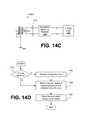
- FIGS. 14A through 14C depict examples of receiving structures that can be employed to receive energy transmitted in the form of a guided surface wave launched by a guided surface waveguide probe according to the various embodiments of the present disclosure.
- FIG. 14D is a flow chart illustrating an example of adjusting a receiving structure according to various embodiments of the present disclosure.
- FIG. 15 depicts an example of an additional receiving structure that can be employed to receive energy transmitted in the form of a guided surface wave launched by a guided surface waveguide probe according to the various embodiments of the present disclosure.
- FIG. 16A depicts a schematic diagram representing the Thevenin-equivalent of the receivers depicted in FIGS. 14A and 14B according to an embodiment of the present disclosure.
- FIG. 16B depicts a schematic diagram representing the Norton-equivalent of the receiver depicted in FIG. 15 according to an embodiment of the present disclosure.
- FIGS. 17A and 17B are schematic diagrams representing examples of a conductivity measurement probe and an open wire line probe, respectively, according to an embodiment of the present disclosure.
- FIG. 18 is a schematic drawing of an example of an adaptive control system employed by the probe control system of FIG. 3 according to various embodiments of the present disclosure.
- FIGS. 19A-19B and 20 are drawings of examples of variable terminals for use as a charging terminal according to various embodiments of the present disclosure.
- a radiated electromagnetic field comprises electromagnetic energy that is emitted from a source structure in the form of waves that are not bound to a waveguide.
- a radiated electromagnetic field is generally a field that leaves an electric structure such as an antenna and propagates through the atmosphere or other medium and is not bound to any waveguide structure. Once radiated electromagnetic waves leave an electric structure such as an antenna, they continue to propagate in the medium of propagation (such as air) independent of their source until they dissipate regardless of whether the source continues to operate. Once electromagnetic waves are radiated, they are not recoverable unless intercepted, and, if not intercepted, the energy inherent in the radiated electromagnetic waves is lost forever.
- Radio structures such as antennas are designed to radiate electromagnetic fields by maximizing the ratio of the radiation resistance to the structure loss resistance. Radiated energy spreads out in space and is lost regardless of whether a receiver is present. The energy density of the radiated fields is a function of distance due to geometric spreading. Accordingly, the term “radiate” in all its forms as used herein refers to this form of electromagnetic propagation.
- a guided electromagnetic field is a propagating electromagnetic wave whose energy is concentrated within or near boundaries between media having different electromagnetic properties.
- a guided electromagnetic field is one that is bound to a waveguide and may be characterized as being conveyed by the current flowing in the waveguide. If there is no load to receive and/or dissipate the energy conveyed in a guided electromagnetic wave, then no energy is lost except for that dissipated in the conductivity of the guiding medium. Stated another way, if there is no load for a guided electromagnetic wave, then no energy is consumed.
- a generator or other source generating a guided electromagnetic field does not deliver real power unless a resistive load is present. To this end, such a generator or other source essentially runs idle until a load is presented.
- FIG. 1 shown is a graph 100 of field strength in decibels (dB) above an arbitrary reference in volts per meter as a function of distance in kilometers on a log-dB plot to further illustrate the distinction between radiated and guided electromagnetic fields.
- the graph 100 of FIG. 1 depicts a guided field strength curve 103 that shows the field strength of a guided electromagnetic field as a function of distance.
- This guided field strength curve 103 is essentially the same as a transmission line mode.
- the graph 100 of FIG. 1 depicts a radiated field strength curve 106 that shows the field strength of a radiated electromagnetic field as a function of distance.
- the radiated field strength curve 106 falls off geometrically (1/d, where d is distance), which is depicted as a straight line on the log-log scale.
- the guided field strength curve 103 has a characteristic exponential decay of e ⁇ d / ⁇ square root over (d) ⁇ and exhibits a distinctive knee 109 on the log-log scale.
- the guided field strength curve 103 and the radiated field strength curve 106 intersect at point 113 , which occurs at a crossing distance. At distances less than the crossing distance at intersection point 113 , the field strength of a guided electromagnetic field is significantly greater at most locations than the field strength of a radiated electromagnetic field.
- the guided and radiated field strength curves 103 and 106 further illustrate the fundamental propagation difference between guided and radiated electromagnetic fields.
- Milligan T., Modern Antenna Design , McGraw-Hill, 1 st Edition, 1985, pp. 8-9, which is incorporated herein by reference in its entirety.
- the wave equation is a differential operator whose eigenfunctions possess a continuous spectrum of eigenvalues on the complex wave-number plane.
- This transverse electro-magnetic (TEM) field is called the radiation field, and those propagating fields are called “Hertzian waves.”
- TEM transverse electro-magnetic
- the wave equation plus boundary conditions mathematically lead to a spectral representation of wave-numbers composed of a continuous spectrum plus a sum of discrete spectra.
- Sommerfeld, A. “Uber die Ausbreitung der Wellen in der Drahtlosen Telegraphie,” Annalen der Physik, Vol. 28, 1909, pp. 665-736.
- ground wave and “surface wave” identify two distinctly different physical propagation phenomena.
- a surface wave arises analytically from a distinct pole yielding a discrete component in the plane wave spectrum. See, e.g., “The Excitation of Plane Surface Waves” by Cullen, A. L., ( Proceedings of the IEE (British), Vol. 101, Part IV, August 1954, pp. 225-235).
- a surface wave is considered to be a guided surface wave.
- the surface wave in the Zenneck-Sommerfeld guided wave sense
- the surface wave is, physically and mathematically, not the same as the ground wave (in the Weyl-Norton-FCC sense) that is now so familiar from radio broadcasting.
- the continuous part of the wave-number eigenvalue spectrum produces the radiation field
- the discrete spectra, and corresponding residue sum arising from the poles enclosed by the contour of integration result in non-TEM traveling surface waves that are exponentially damped in the direction transverse to the propagation.
- Such surface waves are guided transmission line modes.
- Friedman, B. Principles and Techniques of Applied Mathematics , Wiley, 1956, pp. pp. 214, 283-286, 290, 298-300.
- antennas excite the continuum eigenvalues of the wave equation, which is a radiation field, where the outwardly propagating RF energy with E z and H ⁇ in-phase is lost forever.
- waveguide probes excite discrete eigenvalues, which results in transmission line propagation. See Collin, R. E., Field Theory of Guided Waves , McGraw-Hill, 1960, pp. 453, 474-477. While such theoretical analyses have held out the hypothetical possibility of launching open surface guided waves over planar or spherical surfaces of lossy, homogeneous media, for more than a century no known structures in the engineering arts have existed for accomplishing this with any practical efficiency.
- various guided surface waveguide probes are described that are configured to excite electric fields that couple into a guided surface waveguide mode along the surface of a lossy conducting medium.
- Such guided electromagnetic fields are substantially mode-matched in magnitude and phase to a guided surface wave mode on the surface of the lossy conducting medium.
- Such a guided surface wave mode can also be termed a Zenneck waveguide mode.
- the resultant fields excited by the guided surface waveguide probes described herein are substantially mode-matched to a guided surface waveguide mode on the surface of the lossy conducting medium, a guided electromagnetic field in the form of a guided surface wave is launched along the surface of the lossy conducting medium.
- the lossy conducting medium comprises a terrestrial medium such as the Earth.
- FIG. 2 shown is a propagation interface that provides for an examination of the boundary value solutions to Maxwell's equations derived in 1907 by Jonathan Zenneck as set forth in his paper Zenneck, J., “On the Propagation of Plane Electromagnetic Waves Along a Flat Conducting Surface and their Relation to Wireless Telegraphy,” Annalen der Physik, Serial 4, Vol. 23, Sep. 20, 1907, pp. 846-866.
- FIG. 2 depicts cylindrical coordinates for radially propagating waves along the interface between a lossy conducting medium specified as Region 1 and an insulator specified as Region 2.
- Region 1 can comprise, for example, any lossy conducting medium.
- such a lossy conducting medium can comprise a terrestrial medium such as the Earth or other medium.
- Region 2 is a second medium that shares a boundary interface with Region 1 and has different constitutive parameters relative to Region 1.
- Region 2 can comprise, for example, any insulator such as the atmosphere or other medium.
- the reflection coefficient for such a boundary interface goes to zero only for incidence at a complex Brewster angle. See Stratton, J. A., Electromagnetic Theory , McGraw-Hill, 1941, p. 516.
- the present disclosure sets forth various guided surface waveguide probes that generate electromagnetic fields that are substantially mode-matched to a guided surface waveguide mode on the surface of the lossy conducting medium comprising Region 1.
- such electromagnetic fields substantially synthesize a wave front incident at a complex Brewster angle of the lossy conducting medium that can result in zero reflection.
- z is the vertical coordinate normal to the surface of Region 1 and ⁇ is the radial coordinate
- H n (2) ( ⁇ j ⁇ ) is a complex argument Hankel function of the second kind and order n
- u 1 is the propagation constant in the positive vertical (z) direction in Region 1
- u 2 is the propagation constant in the vertical (z) direction in Region 2
- ⁇ 1 is the conductivity of Region 1
- ⁇ is equal to 2 ⁇ f, where f is a frequency of excitation
- ⁇ o is the permittivity of free space
- ⁇ 1 is the permittivity of Region 1
- A is a source constant imposed by the source
- ⁇ is a surface wave radial propagation constant.
- ⁇ r comprises the relative permittivity of Region 1
- ⁇ 1 is the conductivity of Region 1
- ⁇ o is the permittivity of free space
- ⁇ o comprises the permeability of free space.
- Equations (1)-(3) can be considered to be a cylindrically-symmetric, radially-propagating waveguide mode. See Barlow, H. M., and Brown, J., Radio Surface Waves , Oxford University Press, 1962, pp. 10-12, 29-33.
- the present disclosure details structures that excite this “open boundary” waveguide mode.
- a guided surface waveguide probe is provided with a charge terminal of appropriate size that is fed with voltage and/or current and is positioned relative to the boundary interface between Region 2 and Region 1. This may be better understood with reference to FIG.
- FIG. 3 which shows an example of a guided surface waveguide probe 300 a that includes a charge terminal T 1 elevated above a lossy conducting medium 303 (e.g., the earth) along a vertical axis z that is normal to a plane presented by the lossy conducting medium 303 .
- the lossy conducting medium 303 makes up Region 1
- a second medium 306 makes up Region 2 and shares a boundary interface with the lossy conducting medium 303 .
- the lossy conducting medium 303 can comprise a terrestrial medium such as the planet Earth.
- a terrestrial medium comprises all structures or formations included thereon whether natural or man-made.
- such a terrestrial medium can comprise natural elements such as rock, soil, sand, fresh water, sea water, trees, vegetation, and all other natural elements that make up our planet.
- such a terrestrial medium can comprise man-made elements such as concrete, asphalt, building materials, and other man-made materials.
- the lossy conducting medium 303 can comprise some medium other than the Earth, whether naturally occurring or man-made.
- the lossy conducting medium 303 can comprise other media such as man-made surfaces and structures such as automobiles, aircraft, man-made materials (such as plywood, plastic sheeting, or other materials) or other media.
- the second medium 306 can comprise the atmosphere above the ground.
- the atmosphere can be termed an “atmospheric medium” that comprises air and other elements that make up the atmosphere of the Earth.
- the second medium 306 can comprise other media relative to the lossy conducting medium 303 .
- the guided surface waveguide probe 300 a includes a feed network 309 that couples an excitation source 312 to the charge terminal T 1 via, e.g., a vertical feed line conductor.
- a charge Q 1 is imposed on the charge terminal T 1 to synthesize an electric field based upon the voltage applied to terminal T 1 at any given instant.
- ⁇ i angle of incidence
- E electric field
- Equation (14) the radial surface current density of Equation (14) can be restated as
- Equation (1)-(6) I o ⁇ ⁇ 4 ⁇ H 1 ( 2 ) ⁇ ( - j ⁇ ⁇ ⁇ ′ ) .
- Equations (1)-(6) and (17) have the nature of a transmission line mode bound to a lossy interface, not radiation fields that are associated with groundwave propagation. See Barlow, H. M. and Brown, J., Radio Surface Waves , Oxford University Press, 1962, pp. 1-5.
- H n (1) ( x ) J n ( x )+ jN n ( x )
- H n (2) ( x ) J n ( x ) ⁇ jN n ( x )
- These functions represent cylindrical waves propagating radially inward (H n (1) ) and outward (H n (2) ), respectively.
- Equation (20b) and (21) differ in phase by ⁇ square root over (j) ⁇ , which corresponds to an extra phase advance or “phase boost” of 45° or, equivalently, ⁇ /8.
- the “far out” representation predominates over the “close-in” representation of the Hankel function.
- the distance to the Hankel crossover point (or Hankel crossover distance) can be found by equating Equations (20b) and (21) for ⁇ j ⁇ , and solving for R x .
- the Hankel function asymptotes may also vary as the conductivity ( ⁇ ) of the lossy conducting medium changes. For example, the conductivity of the soil can vary with changes in weather conditions.
- Curve 403 is the magnitude of the far-out asymptote of Equation (20b)
- the height H 1 of the elevated charge terminal T 1 in FIG. 3 affects the amount of free charge on the charge terminal T 1 .
- the charge terminal T 1 is near the ground plane of Region 1, most of the charge Q 1 on the terminal is “bound.”
- the bound charge is lessened until the charge terminal T 1 reaches a height at which substantially all of the isolated charge is free.
- the advantage of an increased capacitive elevation for the charge terminal T 1 is that the charge on the elevated charge terminal T 1 is further removed from the ground plane, resulting in an increased amount of free charge q free to couple energy into the guided surface waveguide mode. As the charge terminal T 1 is moved away from the ground plane, the charge distribution becomes more uniformly distributed about the surface of the terminal. The amount of free charge is related to the self-capacitance of the charge terminal T 1 .
- the capacitance of a spherical terminal can be expressed as a function of physical height above the ground plane.
- an increase in the terminal height h reduces the capacitance C of the charge terminal.
- the charge distribution is approximately uniform about the spherical terminal, which can improve the coupling into the guided surface waveguide mode.
- the charge terminal T 1 can include any shape such as a sphere, a disk, a cylinder, a cone, a torus, a hood, one or more rings, or any other randomized shape or combination of shapes.
- An equivalent spherical diameter can be determined and used for positioning of the charge terminal T 1 .
- the charge terminal T 1 can be positioned at a physical height that is at least four times the spherical diameter (or equivalent spherical diameter) of the charge terminal T 1 to reduce the bounded charge effects.
- FIG. 5A shown is a ray optics interpretation of the electric field produced by the elevated charge Q 1 on charge terminal T 1 of FIG. 3 .
- minimizing the reflection of the incident electric field can improve and/or maximize the energy coupled into the guided surface waveguide mode of the lossy conducting medium 303 .
- the amount of reflection of the incident electric field may be determined using the Fresnel reflection coefficient, which can be expressed as
- the ray optic interpretation shows the incident field polarized parallel to the plane of incidence having an angle of incidence of ⁇ i , which is measured with respect to the surface normal ( ⁇ circumflex over (z) ⁇ ).
- ⁇ i angle of incidence
- This complex angle of incidence ( ⁇ i,B ) is referred to as the Brewster angle.
- Equation (22) it can be seen that the same complex Brewster angle ( ⁇ i,B ) relationship is present in both Equations (22) and (26).
- the electric field vector E can be depicted as an incoming non-uniform plane wave, polarized parallel to the plane of incidence.
- the illustration in FIG. 5A suggests that the electric field vector E can be given by
- E ⁇ ⁇ ( ⁇ , z ) E ⁇ ( ⁇ , z ) ⁇ cos ⁇ ⁇ ⁇ i , and ( 28 ⁇ a )
- a generalized parameter W is noted herein as the ratio of the horizontal electric field component to the vertical electric field component given by
- the wave tilt angle ( ⁇ ) is equal to the angle between the normal of the wave-front at the boundary interface with Region 1 and the tangent to the boundary interface. This may be easier to see in FIG. 5B , which illustrates equi-phase surfaces of an electromagnetic wave and their normals for a radial cylindrical guided surface wave.
- Equation (30b) Applying Equation (30b) to a guided surface wave gives
- the concept of an electrical effective height can provide further insight into synthesizing an electric field with a complex angle of incidence with a guided surface waveguide probe 300 .
- the electrical effective height (h eff ) has been defined as
- h eff 1 I 0 ⁇ ⁇ ⁇ 0 h p ⁇ I ⁇ ( z ) ⁇ d ⁇ ⁇ z ( 33 ) for a monopole with a physical height (or length) of h p . Since the expression depends upon the magnitude and phase of the source distribution along the structure, the effective height (or length) is complex in general.
- the integration of the distributed current I(z) of the structure is performed over the physical height of the structure (h p ), and normalized to the ground current (I 0 ) flowing upward through the base (or input) of the structure.
- I C is the current that is distributed along the vertical structure of the guided surface waveguide probe 300 a.
- a feed network 309 that includes a low loss coil (e.g., a helical coil) at the bottom of the structure and a vertical feed line conductor connected between the coil and the charge terminal T 1 .
- V f is the velocity factor on the structure
- ⁇ 0 is the wavelength at the supplied frequency
- ⁇ p is the propagation wavelength resulting from the velocity factor V f .
- the phase delay is measured relative to the ground (stake) current I 0 .
- the electrical effective height of a guided surface waveguide probe 300 can be approximated by
- h eff 1 I 0 ⁇ ⁇ 0 h p ⁇ I 0 ⁇ e j ⁇ ⁇ ⁇ ⁇ cos ⁇ ( ⁇ 0 ⁇ z ) ⁇ d ⁇ ⁇ z ⁇ h p ⁇ e j ⁇ ⁇ ⁇ , ( 37 ) for the case where the physical height h p ⁇ 0 .
- ray optics are used to illustrate the complex angle trigonometry of the incident electric field (E) having a complex Brewster angle of incidence ( ⁇ i,B ) at the Hankel crossover distance (R x ) 315 .
- Equation (26) that, for a lossy conducting medium, the Brewster angle is complex and specified by
- the wave tilt of the electric field at the Hankel crossover distance can be expressed as the ratio of the electrical effective height and the Hankel crossover distance
- a right triangle is depicted having an adjacent side of length R x along the lossy conducting medium surface and a complex Brewster angle ⁇ i,B measured between a ray 316 extending between the Hankel crossover point 315 at R x and the center of the charge terminal T 1 , and the lossy conducting medium surface 317 between the Hankel crossover point 315 and the charge terminal T 1 .
- the charge terminal T 1 positioned at physical height h p and excited with a charge having the appropriate phase delay ⁇ , the resulting electric field is incident with the lossy conducting medium boundary interface at the Hankel crossover distance R x , and at the Brewster angle. Under these conditions, the guided surface waveguide mode can be excited without reflection or substantially negligible reflection.
- FIG. 6 graphically illustrates the effect of decreasing the physical height of the charge terminal T 1 on the distance where the electric field is incident at the Brewster angle.
- the point where the electric field intersects with the lossy conducting medium (e.g., the earth) at the Brewster angle moves closer to the charge terminal position.
- Equation (39) indicates, the height H 1 ( FIG.
- the height of the charge terminal T 1 should be at or higher than the physical height (h p ) in order to excite the far-out component of the Hankel function.
- the height should be at least four times the spherical diameter (or equivalent spherical diameter) of the charge terminal T 1 as mentioned above.
- a guided surface waveguide probe 300 can be configured to establish an electric field having a wave tilt that corresponds to a wave illuminating the surface of the lossy conducting medium 303 at a complex Brewster angle, thereby exciting radial surface currents by substantially mode-matching to a guided surface wave mode at (or beyond) the Hankel crossover point 315 at R x .
- FIG. 7 shown is a graphical representation of an example of a guided surface waveguide probe 300 b that includes a charge terminal T 1 .
- An AC source 712 acts as the excitation source ( 312 of FIG. 3 ) for the charge terminal T 1 , which is coupled to the guided surface waveguide probe 300 b through a feed network ( 309 of FIG.
- the AC source 712 can be inductively coupled to the coil 709 through a primary coil.
- an impedance matching network may be included to improve and/or maximize coupling of the AC source 712 to the coil 709 .
- the guided surface waveguide probe 300 b can include the upper charge terminal T 1 (e.g., a sphere at height h p ) that is positioned along a vertical axis z that is substantially normal to the plane presented by the lossy conducting medium 303 .
- a second medium 306 is located above the lossy conducting medium 303 .
- the charge terminal T 1 has a self-capacitance C T .
- charge Q 1 is imposed on the terminal T 1 depending on the voltage applied to the terminal T 1 at any given instant.
- the coil 709 is coupled to a ground stake 715 at a first end and to the charge terminal T 1 via a vertical feed line conductor 718 .
- the coil connection to the charge terminal T 1 can be adjusted using a tap 721 of the coil 709 as shown in FIG. 7 .
- the coil 709 can be energized at an operating frequency by the AC source 712 through a tap 724 at a lower portion of the coil 709 .
- the AC source 712 can be inductively coupled to the coil 709 through a primary coil.
- the construction and adjustment of the guided surface waveguide probe 300 is based upon various operating conditions, such as the transmission frequency, conditions of the lossy conducting medium (e.g., soil conductivity a and relative permittivity ⁇ r ), and size of the charge terminal T 1 .
- the conductivity a and relative permittivity ⁇ r can be determined through test measurements of the lossy conducting medium 303 .
- Equation ( 43 ) The wave tilt at the Hankel crossover distance (w Rx ) can also be found using Equation (40).
- the Hankel crossover distance can also be found by equating the magnitudes of Equations (20b) and (21) for ⁇ j ⁇ , and solving for R x as illustrated by FIG. 4 .
- the complex effective height (h eff ) includes a magnitude that is associated with the physical height (h p ) of the charge terminal T 1 and a phase delay ( ⁇ ) that is to be associated with the angle ( ⁇ ) of the wave tilt at the Hankel crossover distance (R x ).
- the feed network ( 309 of FIG. 3 ) and/or the vertical feed line connecting the feed network to the charge terminal T 1 can be adjusted to match the phase ( ⁇ ) of the charge Q 1 on the charge terminal T 1 to the angle ( ⁇ ) of the wave tilt (W).
- the size of the charge terminal T 1 can be chosen to provide a sufficiently large surface for the charge Q 1 imposed on the terminals. In general, it is desirable to make the charge terminal T 1 as large as practical. The size of the charge terminal T 1 should be large enough to avoid ionization of the surrounding air, which can result in electrical discharge or sparking around the charge terminal.
- phase delay ⁇ c of a helically-wound coil can be determined from Maxwell's equations as has been discussed by Corum, K. L. and J. F. Corum, “RF Coils, Helical Resonators and Voltage Magnification by Coherent Spatial Modes,” Microwave Review , Vol. 7, No. 2, September 2001, pp. 36-45., which is incorporated herein by reference in its entirety.
- H/D the ratio of the velocity of propagation (v) of a wave along the coil's longitudinal axis to the speed of light (c), or the “velocity factor”
- H is the axial length of the solenoidal helix
- D is the coil diameter
- N is the number of turns of the coil
- ⁇ o is the free-space wavelength.
- the principle is the same if the helix is wound spirally or is short and fat, but V f and ⁇ c are easier to obtain by experimental measurement.
- the expression for the characteristic (wave) impedance of a helical transmission line has also been derived as
- the spatial phase delay ⁇ y of the structure can be determined using the traveling wave phase delay of the vertical feed line conductor 718 ( FIG. 7 ).
- the capacitance of a cylindrical vertical conductor above a prefect ground plane can be expressed as
- ⁇ w is the propagation phase constant for the vertical feed line conductor
- h w is the vertical length (or height) of the vertical feed line conductor
- V w is the velocity factor on the wire
- ⁇ 0 is the wavelength at the supplied frequency
- ⁇ W is the propagation wavelength resulting from the velocity factor V w .
- the velocity factor is a constant with V w ⁇ 0.94, or in a range from about 0.93 to about 0.98. If the mast is considered to be a uniform transmission line, its average characteristic impedance can be approximated by
- Equation (51) implies that Z o for a single-wire feeder varies with frequency.
- the phase delay can be determined based upon the capacitance and characteristic impedance.
- the electric field produced by the charge oscillating Q 1 on the charge terminal T 1 is coupled into a guided surface waveguide mode traveling along the surface of a lossy conducting medium 303 .
- the Brewster angle ( ⁇ i,B ) the phase delay ( ⁇ y ) associated with the vertical feed line conductor 718 ( FIG. 7 ), and the configuration of the coil 709 ( FIG.
- the position of the tap 721 may be adjusted to maximize coupling the traveling surface waves into the guided surface waveguide mode. Excess coil length beyond the position of the tap 721 can be removed to reduce the capacitive effects.
- the vertical wire height and/or the geometrical parameters of the helical coil may also be varied.
- the coupling to the guided surface waveguide mode on the surface of the lossy conducting medium 303 can be improved and/or optimized by tuning the guided surface waveguide probe 300 for standing wave resonance with respect to a complex image plane associated with the charge Q 1 on the charge terminal T 1 .
- the performance of the guided surface waveguide probe 300 can be adjusted for increased and/or maximum voltage (and thus charge Q 1 ) on the charge terminal T 1 .
- the effect of the lossy conducting medium 303 in Region 1 can be examined using image theory analysis.
- an elevated charge Q 1 placed over a perfectly conducting plane attracts the free charge on the perfectly conducting plane, which then “piles up” in the region under the elevated charge Q 1 .
- the resulting distribution of “bound” electricity on the perfectly conducting plane is similar to a bell-shaped curve.
- the boundary value problem solution that describes the fields in the region above the perfectly conducting plane may be obtained using the classical notion of image charges, where the field from the elevated charge is superimposed with the field from a corresponding “image” charge below the perfectly conducting plane.
- This analysis may also be used with respect to a lossy conducting medium 303 by assuming the presence of an effective image charge Q 1 ′ beneath the guided surface waveguide probe 300 .
- the effective image charge Q 1 ′ coincides with the charge Q 1 on the charge terminal T 1 about a conducting image ground plane 318 , as illustrated in FIG. 3 .
- the image charge Q 1 ′ is not merely located at some real depth and 180° out of phase with the primary source charge Q 1 on the charge terminal T 1 , as they would be in the case of a perfect conductor. Rather, the lossy conducting medium 303 (e.g., a terrestrial medium) presents a phase shifted image.
- the image charge Q 1 ′ is at a complex depth below the surface (or physical boundary) of the lossy conducting medium 303 .
- complex image depth reference is made to Wait, J. R., “Complex Image Theory—Revisited,” IEEE Antennas and Propagation Magazine , Vol. 33, No. 4, August 1991, pp. 27-29, which is incorporated herein by reference in its entirety.
- ⁇ e 2 j ⁇ 1 ⁇ 1 ⁇ 2 ⁇ 1 ⁇ 1
- k o ⁇ square root over ( ⁇ o ⁇ o ) ⁇ . (54) as indicated in Equation (12).
- the complex spacing of the image charge implies that the external field will experience extra phase shifts not encountered when the interface is either a dielectric or a perfect conductor.
- the lossy conducting medium 303 is a finitely conducting earth 803 with a physical boundary 806 .
- the finitely conducting earth 803 may be replaced by a perfectly conducting image ground plane 809 as shown in FIG. 8B , which is located at a complex depth z 1 below the physical boundary 806 .
- This equivalent representation exhibits the same impedance when looking down into the interface at the physical boundary 806 .
- the equivalent representation of FIG. 8B can be modeled as an equivalent transmission line, as shown in FIG. 8C .
- the depth z 1 can be determined by equating the TEM wave impedance looking down at the earth to an image ground plane impedance z in seen looking into the transmission line of FIG. 8C .
- the distance to the perfectly conducting image ground plane 809 can be approximated by
- the guided surface waveguide probe 300 b of FIG. 7 can be modeled as an equivalent single-wire transmission line image plane model that can be based upon the perfectly conducting image ground plane 809 of FIG. 8B .
- FIG. 9A shows an example of the equivalent single-wire transmission line image plane model
- FIG. 9B illustrates an example of the equivalent classic transmission line model, including the shorted transmission line of FIG. 8C .
- Z w is the characteristic impedance of the elevated vertical feed line conductor 718 in ohms
- Z c is the characteristic impedance of the coil 709 in ohms
- Z o is the characteristic impedance of free space.
- Z ⁇ Z in , which is given by:
- the impedance at the physical boundary 806 “looking up” into the guided surface waveguide probe 300 is the conjugate of the impedance at the physical boundary 806 “looking down” into the lossy conducting medium 303 .
- the equivalent image plane models of FIGS. 9A and 9B can be tuned to resonance with respect to the image ground plane 809 .
- the impedance of the equivalent complex image plane model is purely resistive, which maintains a superposed standing wave on the probe structure that maximizes the voltage and elevated charge on terminal T 1 , and by equations (1)-(3) and (16) maximizes the propagating surface wave.
- the guided surface wave excited by the guided surface waveguide probe 300 is an outward propagating traveling wave.
- the source distribution along the feed network 309 between the charge terminal T 1 and the ground stake 715 of the guided surface waveguide probe 300 ( FIGS. 3 and 7 ) is actually composed of a superposition of a traveling wave plus a standing wave on the structure.
- the phase delay of the traveling wave moving through the feed network 309 is matched to the angle of the wave tilt associated with the lossy conducting medium 303 . This mode-matching allows the traveling wave to be launched along the lossy conducting medium 303 .
- the load impedance Z L of the charge terminal T 1 is adjusted to bring the probe structure into standing wave resonance with respect to the image ground plane ( 318 of FIG. 3 or 809 of FIG. 8 ), which is at a complex depth of ⁇ d/2. In that case, the impedance seen from the image ground plane has zero reactance and the charge on the charge terminal T 1 is maximized.
- the effect of such discontinuous phase jumps can be seen in the Smith chart plots in FIG. 12 .
- two relatively short transmission line sections of widely differing characteristic impedance may be used to provide a very large phase shift.
- a probe structure composed of two sections of transmission line, one of low impedance and one of high impedance, together totaling a physical length of, say, 0.05 ⁇ , may be fabricated to provide a phase shift of 90° which is equivalent to a 0.25 ⁇ resonance. This is due to the large jump in characteristic impedances.
- a physically short probe structure can be electrically longer than the two physical lengths combined. This is illustrated in FIGS. 9A and 9B , but is especially clear in FIG. 12 where the discontinuities in the impedance ratios provide large jumps in phase between the different plotted sections on the Smith chart.
- the impedance discontinuity provides a substantial phase shift where the sections are joined together.
- FIG. 10 shown is a flow chart illustrating an example of adjusting a guided surface waveguide probe 300 ( FIG. 3 ) to substantially mode-match to a guided surface waveguide mode on the surface of the lossy conducting medium, which launches a guided surface traveling wave along the surface of a lossy conducting medium 303 ( FIG. 3 ).
- the charge terminal T 1 of the guided surface waveguide probe 300 is positioned at a defined height above a lossy conducting medium 303 .
- the Hankel crossover distance can also be found by equating the magnitudes of Equations (20b) and (21) for ⁇ j ⁇ , and solving for R x as illustrated by FIG.
- the complex index of refraction (n) can be determined using Equation (41) and the complex Brewster angle ( ⁇ i,B ) can then be determined from Equation (42).
- the physical height (h p ) of the charge terminal T 1 can then be determined from Equation (44).
- the charge terminal T 1 should be at or higher than the physical height (h p ) in order to excite the far-out component of the Hankel function. This height relationship is initially considered when launching surface waves. To reduce or minimize the bound charge on the charge terminal T 1 , the height should be at least four times the spherical diameter (or equivalent spherical diameter) of the charge terminal T 1 .
- the electrical phase delay D of the elevated charge Q 1 on the charge terminal T 1 is matched to the complex wave tilt angle ⁇ .
- the phase delay ( ⁇ c ) of the helical coil and/or the phase delay ( ⁇ y ) of the vertical feed line conductor can be adjusted to make ⁇ equal to the angle ( ⁇ ) of the wave tilt (W). Based on Equation (31), the angle ( ⁇ ) of the wave tilt can be determined from:
- the electrical phase ⁇ can then be matched to the angle of the wave tilt. This angular (or phase) relationship is next considered when launching surface waves.
- the load impedance of the charge terminal T 1 is tuned to resonate the equivalent image plane model of the guided surface waveguide probe 300 .
- the depth (d/2) of the conducting image ground plane 809 (or 318 of FIG. 3 ) can be determined using Equations (52), (53) and (54) and the values of the lossy conducting medium 303 (e.g., the earth), which can be measured.
- the impedance (Z in ) as seen “looking down” into the lossy conducting medium 303 can then be determined using Equation (65). This resonance relationship can be considered to maximize the launched surface waves.
- the velocity factor, phase delay, and impedance of the coil 709 and vertical feed line conductor 718 can be determined using Equations (45) through (51).
- the self-capacitance (C T ) of the charge terminal T 1 can be determined using, e.g., Equation (24).
- the propagation factor ( ⁇ p ) of the coil 709 can be determined using Equation (35) and the propagation phase constant ( ⁇ w ) for the vertical feed line conductor 718 can be determined using Equation (49).
- the impedance (Z base ) of the guided surface waveguide probe 300 as seen “looking up” into the coil 709 can be determined using Equations (62), (63) and (64).
- the impedance at the physical boundary 806 “looking up” into the guided surface waveguide probe 300 is the conjugate of the impedance at the physical boundary 806 “looking down” into the lossy conducting medium 303 .
- An iterative approach may be taken to tune the load impedance Z L for resonance of the equivalent image plane model with respect to the conducting image ground plane 809 (or 318 ). In this way, the coupling of the electric field to a guided surface waveguide mode along the surface of the lossy conducting medium 303 (e.g., earth) can be improved and/or maximized.
- the lossy conducting medium 303 e.g., earth
- a guided surface waveguide probe 300 comprising a top-loaded vertical stub of physical height h p with a charge terminal T 1 at the top, where the charge terminal T 1 is excited through a helical coil and vertical feed line conductor at an operational frequency (f o ) of 1.85 MHz.
- f o operational frequency
- the wave length can be determined as:
- Equation (66) the wave tilt values can be determined to be:
- the velocity factor of the vertical feed line conductor (approximated as a uniform cylindrical conductor with a diameter of 0.27 inches) can be given as V w ⁇ 0.93. Since h p ⁇ o , the propagation phase constant for the vertical feed line conductor can be approximated as:
- ⁇ will equal ⁇ to match the guided surface waveguide mode.
- FIG. 11 shows a plot of both over a range of frequencies. As both ⁇ and ⁇ are frequency dependent, it can be seen that their respective curves cross over each other at approximately 1.85 MHz.
- Equation (45) For a helical coil having a conductor diameter of 0.0881 inches, a coil diameter (D) of 30 inches and a turn-to-turn spacing (s) of 4 inches, the velocity factor for the coil can be determined using Equation (45) as:
- Equation (46) the axial length of the solenoidal helix (H) can be determined using Equation (46) such that:
- the load impedance (Z L ) of the charge terminal T 1 can be adjusted for standing wave resonance of the equivalent image plane model of the guided surface wave probe 300 .
- Equation (52) Equation (52)
- the coupling into the guided surface waveguide mode may be maximized. This can be accomplished by adjusting the capacitance of the charge terminal T 1 without changing the traveling wave phase delays of the coil and vertical feed line conductor. For example, by adjusting the charge terminal capacitance (C T ) to 61.8126 pF, the load impedance from Equation (62) is:
- Equation (51) the impedance of the vertical feed line conductor (having a diameter (2a) of 0.27 inches) is given as
- Equation (63) the impedance seen “looking up” into the vertical feed line conductor is given by Equation (63) as:
- Equation (64) the impedance seen “looking up” into the coil at the base is given by Equation (64) as:
- a Smith chart 1200 that graphically illustrates an example of the effect of the discontinuous phase jumps on the impedance (Z ip ) seen “looking up” into the equivalent image plane model of FIG. 9B .
- Z ip the impedance
- the actual load impedance Z L is normalized with respect to the characteristic impedance (Z w ) of the vertical feed line conductor and is entered on Smith chart 1200 at point 1203 (Z L /Z w ).
- the impedance at point 1206 is now converted to the actual impedance (Z 2 ) seen “looking up” into the vertical feed line conductor using Z w .
- the impedance Z 2 is then normalized with respect to the characteristic impedance (Z c ) of the helical coil.
- the jump between point 1206 and point 1209 is a result of the discontinuity in the impedance ratios.
- the impedance looking into the base of the coil at point 1212 is then converted to the actual impedance (Z base ) seen “looking up” into the base of the coil (or the guided surface wave probe 300 ) using Z c .
- the impedance at Z base is then normalized with respect to the characteristic impedance (Z o ) of the modeled image space below the physical boundary of the lossy conducting medium (e.g., the ground surface).
- the jump between point 1212 and point 1215 is a result of the discontinuity in the impedance ratios.
- the impedance looking into the subsurface image transmission line at point 1218 is now converted to an actual impedance (Z ip ) using Z o .
- Z ip R ip +j0.
- Z base /Z o is a larger reactance than Z base /Z c . This is because the characteristic impedance (Z c ) of a helical coil is considerably larger than the characteristic impedance Z o of free space.
- the above example illustrates how the three considerations discussed above can be satisfied for launching guided surface traveling waves on the lossy conducting medium.
- Field strength measurements were carried out to verify the ability of the guided surface waveguide probe 300 b ( FIG. 7 ) to couple into a guided surface wave or a transmission line mode.
- the measured data (documented with a NIST-traceable field strength meter) is tabulated below in TABLE 1.
- FIG. 13 shown is the measured field strength in mV/m (circles) vs. range (in miles) with respect to the theoretical Zenneck surface wave field strengths for 100% and 85% electric charge, as well as the conventional Norton radiated ground-wave predicted for a 16 foot top-loaded vertical mast (monopole at 2.5% radiation efficiency).
- the quantity h corresponds to the height of the vertical conducting mast for Norton ground wave radiation with a 55 ohm ground stake.
- the predicted Zenneck fields were calculated from Equation (3), and the standard Norton ground wave was calculated by conventional means. A statistical analysis gave a minimized RMS deviation between the measured and theoretical fields for an electrical efficiency of 97.4%.
- the guided field strength curve 103 of the guided electromagnetic field has a characteristic exponential decay of e ⁇ d / ⁇ square root over (d) ⁇ and exhibits a distinctive knee 109 on the log-log scale.
- the charge terminal T 1 is of sufficient height H 1 of FIG. 3 (h ⁇ R x tan ⁇ i,B ) so that electromagnetic waves incident onto the lossy conducting medium 303 at the complex Brewster angle do so out at a distance ( ⁇ R x ) where the 1/ ⁇ square root over (r) ⁇ term is predominant.
- Receive circuits can be utilized with one or more guided surface waveguide probes to facilitate wireless transmission and/or power delivery systems.
- FIGS. 14A, 14B, 14C and 15 shown are examples of generalized receive circuits for using the surface-guided waves in wireless power delivery systems.
- FIGS. 14A and 14B-14C include a linear probe 1403 and a tuned resonator 1406 , respectively.
- FIG. 15 is a magnetic coil 1409 according to various embodiments of the present disclosure.
- each one of the linear probe 1403 , the tuned resonator 1406 , and the magnetic coil 1409 may be employed to receive power transmitted in the form of a guided surface wave on the surface of a lossy conducting medium 303 ( FIG. 3 ) according to various embodiments.
- the lossy conducting medium 303 comprises a terrestrial medium (or earth).
- the open-circuit terminal voltage at the output terminals 1413 of the linear probe 1403 depends upon the effective height of the linear probe 1403 .
- An electrical load 1416 is coupled to the output terminals 1413 through an impedance matching network 1419 .
- the electrical load 1416 should be substantially impedance matched to the linear probe 1403 as will be described below.
- a ground current excited coil 1406 a possessing a phase shift equal to the wave tilt of the guided surface wave includes a charge terminal T R that is elevated (or suspended) above the lossy conducting medium 303 .
- the charge terminal T R has a self-capacitance C R .
- the bound capacitance should preferably be minimized as much as is practicable, although this may not be entirely necessary in every instance of a guided surface waveguide probe 300 .
- the tuned resonator 1406 a also includes a receiver network comprising a coil L R having a phase shift ⁇ . One end of the coil L R is coupled to the charge terminal T R , and the other end of the coil L R is coupled to the lossy conducting medium 303 .
- the receiver network can include a vertical supply line conductor that couples the coil L R to the charge terminal T R .
- the coil 1406 a (which may also be referred to as tuned resonator L R -C R ) comprises a series-adjusted resonator as the charge terminal C R and the coil L R are situated in series.
- the phase delay of the coil 1406 a can be adjusted by changing the size and/or height of the charge terminal T R , and/or adjusting the size of the coil L R so that the phase ⁇ of the structure is made substantially equal to the angle of the wave tilt ⁇ .
- the phase delay of the vertical supply line can also be adjusted by, e.g., changing length of the conductor.
- the reactance presented by the self-capacitance C R is calculated as 1/j ⁇ C R .
- the total capacitance of the structure 1406 a may also include capacitance between the charge terminal T R and the lossy conducting medium 303 , where the total capacitance of the structure 1406 a may be calculated from both the self-capacitance C R and any bound capacitance as can be appreciated.
- the charge terminal T R may be raised to a height so as to substantially reduce or eliminate any bound capacitance. The existence of a bound capacitance may be determined from capacitance measurements between the charge terminal T R and the lossy conducting medium 303 as previously discussed.
- the inductive reactance presented by a discrete-element coil L R may be calculated as j ⁇ L, where L is the lumped-element inductance of the coil L R . If the coil L R is a distributed element, its equivalent terminal-point inductive reactance may be determined by conventional approaches.
- To tune the structure 1406 a one would make adjustments so that the phase delay is equal to the wave tilt for the purpose of mode-matching to the surface waveguide at the frequency of operation. Under this condition, the receiving structure may be considered to be “mode-matched” with the surface waveguide.
- a transformer link around the structure and/or an impedance matching network 1423 may be inserted between the probe and the electrical load 1426 in order to couple power to the load. Inserting the impedance matching network 1423 between the probe terminals 1421 and the electrical load 1426 can effect a conjugate-match condition for maximum power transfer to the electrical load 1426 .
- an electrical load 1426 When placed in the presence of surface currents at the operating frequencies power will be delivered from the surface guided wave to the electrical load 1426 .
- an electrical load 1426 may be coupled to the structure 1406 a by way of magnetic coupling, capacitive coupling, or conductive (direct tap) coupling.
- the elements of the coupling network may be lumped components or distributed elements as can be appreciated.
- magnetic coupling is employed where a coil L s is positioned as a secondary relative to the coil L R that acts as a transformer primary.
- the coil L s may be link-coupled to the coil L R by geometrically winding it around the same core structure and adjusting the coupled magnetic flux as can be appreciated.
- the receiving structure 1406 a comprises a series-tuned resonator, a parallel-tuned resonator or even a distributed-element resonator of the appropriate phase delay may also be used.
- a receiving structure immersed in an electromagnetic field may couple energy from the field
- polarization-matched structures work best by maximizing the coupling, and conventional rules for probe-coupling to waveguide modes should be observed.
- a TE 20 (transverse electric mode) waveguide probe may be optimal for extracting energy from a conventional waveguide excited in the TE 20 mode.
- a mode-matched and phase-matched receiving structure can be optimized for coupling power from a surface-guided wave.
- the guided surface wave excited by a guided surface waveguide probe 300 on the surface of the lossy conducting medium 303 can be considered a waveguide mode of an open waveguide. Excluding waveguide losses, the source energy can be completely recovered.
- Useful receiving structures may be E-field coupled, H-field coupled, or surface-current excited.
- the receiving structure can be adjusted to increase or maximize coupling with the guided surface wave based upon the local characteristics of the lossy conducting medium 303 in the vicinity of the receiving structure.
- a receiving structure comprising the tuned resonator 1406 a of FIG. 14B , including a coil L R and a vertical supply line connected between the coil L R and a charge terminal T R .
- the charge terminal T R positioned at a defined height above the lossy conducting medium 303 .
- the total phase shift ⁇ of the coil L R and vertical supply line can be matched with the angle ( ⁇ ) of the wave tilt at the location of the tuned resonator 1406 a . From Equation (22), it can be seen that the wave tilt asymptotically passes to
- ⁇ r comprises the relative permittivity
- ⁇ 1 is the conductivity of the lossy conducting medium 303 at the location of the receiving structure
- ⁇ o is the permittivity of free space
- ⁇ 2 ⁇ f, where f is the frequency of excitation.
- the wave tilt angle ( ⁇ ) can be determined from Equation (86).
- phase delays ( ⁇ c + ⁇ y ) can be adjusted to match the phase shift ⁇ to the angle ( ⁇ ) of the wave tilt.
- a portion of the coil can be bypassed by the tap connection as illustrated in FIG. 14B .
- the vertical supply line conductor can also be connected to the coil L R via a tap, whose position on the coil may be adjusted to match the total phase shift to the angle of the wave tilt.
- Z ⁇ Z base as illustrated in FIG. 9A .
- the coupling into the guided surface waveguide mode may be maximized.
- the tuned resonator 1406 b does not include a charge terminal T R at the top of the receiving structure.
- the tuned resonator 1406 b does not include a vertical supply line coupled between the coil L R and the charge terminal T R .
- the total phase shift ( ⁇ ) of the tuned resonator 1406 b includes only the phase delay ( ⁇ c ) through the coil L R .
- FIG. 14D shown is a flow chart illustrating an example of adjusting a receiving structure to substantially mode-match to a guided surface waveguide mode on the surface of the lossy conducting medium 303 .
- the receiving structure includes a charge terminal T R (e.g., of the tuned resonator 1406 a of FIG. 14B )
- the charge terminal T R is positioned at a defined height above a lossy conducting medium 303 at 1456 .
- the physical height (h p ) of the charge terminal T R height may be below that of the effective height.
- the physical height may be selected to reduce or minimize the bound charge on the charge terminal T R (e.g., four times the spherical diameter of the charge terminal). If the receiving structure does not include a charge terminal T R (e.g., of the tuned resonator 1406 b of FIG. 14C ), then the flow proceeds to 1459 .
- the electrical phase delay ⁇ of the receiving structure is matched to the complex wave tilt angle ⁇ defined by the local characteristics of the lossy conducting medium 303 .
- the phase delay ( ⁇ c ) of the helical coil and/or the phase delay ( ⁇ y ) of the vertical supply line can be adjusted to make ⁇ equal to the angle ( ⁇ ) of the wave tilt (W).
- the angle ( ⁇ ) of the wave tilt can be determined from Equation (86).
- the electrical phase ⁇ can then be matched to the angle of the wave tilt.
- the load impedance of the charge terminal T R can be tuned to resonate the equivalent image plane model of the tuned resonator 1406 a .
- the depth (d/2) of the conducting image ground plane 809 ( FIG. 9A ) below the receiving structure can be determined using Equation (89) and the values of the lossy conducting medium 303 (e.g., the earth) at the receiving structure, which can be locally measured.
- the impedance (Z in ) as seen “looking down” into the lossy conducting medium 303 can then be determined using Equation (88). This resonance relationship can be considered to maximize coupling with the guided surface waves.
- the velocity factor, phase delay, and impedance of the coil L R and vertical supply line can be determined.
- the self-capacitance (C R ) of the charge terminal T R can be determined using, e.g., Equation (24).
- the propagation factor ( ⁇ p ) of the coil L R can be determined using Equation (87) and the propagation phase constant ( ⁇ w ) for the vertical supply line can be determined using Equation (49).
- the impedance (Z base ) of the tuned resonator 1406 a as seen “looking up” into the coil L R can be determined using Equations (90), (91), and (92).
- the equivalent image plane model of FIG. 9A also applies to the tuned resonator 1406 a of FIG. 14B .
- the impedance at the physical boundary 806 ( FIG. 9A ) “looking up” into the coil of the tuned resonator 1406 a is the conjugate of the impedance at the physical boundary 806 “looking down” into the lossy conducting medium 303 .
- An iterative approach may be taken to tune the load impedance Z R for resonance of the equivalent image plane model with respect to the conducting image ground plane 809 . In this way, the coupling of the electric field to a guided surface waveguide mode along the surface of the lossy conducting medium 303 (e.g., earth) can be improved and/or maximized.
- the magnetic coil 1409 comprises a receive circuit that is coupled through an impedance matching network 1433 to an electrical load 1436 .
- the magnetic coil 1409 may be positioned so that the magnetic flux of the guided surface wave, H ⁇ , passes through the magnetic coil 1409 , thereby inducing a current in the magnetic coil 1409 and producing a terminal point voltage at its output terminals 1429 .
- the open-circuit induced voltage appearing at the output terminals 1429 of the magnetic coil 1409 is
- the magnetic coil 1409 may be tuned to the guided surface wave frequency either as a distributed resonator or with an external capacitor across its output terminals 1429 , as the case may be, and then impedance-matched to an external electrical load 1436 through a conjugate impedance matching network 1433 .
- the current induced in the magnetic coil 1409 may be employed to optimally power the electrical load 1436 .
- the receive circuit presented by the magnetic coil 1409 provides an advantage in that it does not have to be physically connected to the ground.
- the receive circuits presented by the linear probe 1403 , the mode-matched structure 1406 , and the magnetic coil 1409 each facilitate receiving electrical power transmitted from any one of the embodiments of guided surface waveguide probes 300 described above.
- the energy received may be used to supply power to an electrical load 1416 / 1426 / 1436 via a conjugate matching network as can be appreciated.
- the receive circuits presented by the linear probe 1403 , the mode-matched structure 1406 , and the magnetic coil 1409 will load the excitation source 312 ( FIG. 3 ) that is applied to the guided surface waveguide probe 300 , thereby generating the guided surface wave to which such receive circuits are subjected.
- the guided surface wave generated by a given guided surface waveguide probe 300 described above comprises a transmission line mode.
- a power source that drives a radiating antenna that generates a radiated electromagnetic wave is not loaded by the receivers, regardless of the number of receivers employed.
- one or more guided surface waveguide probes 300 and one or more receive circuits in the form of the linear probe 1403 , the tuned mode-matched structure 1406 , and/or the magnetic coil 1409 can together make up a wireless distribution system.
- the distance of transmission of a guided surface wave using a guided surface waveguide probe 300 as set forth above depends upon the frequency, it is possible that wireless power distribution can be achieved across wide areas and even globally.
- the conventional wireless-power transmission/distribution systems extensively investigated today include “energy harvesting” from radiation fields and also sensor coupling to inductive or reactive near-fields.
- the present wireless-power system does not waste power in the form of radiation which, if not intercepted, is lost forever.
- the presently disclosed wireless-power system limited to extremely short ranges as with conventional mutual-reactance coupled near-field systems.
- the wireless-power system disclosed herein probe-couples to the novel surface-guided transmission line mode, which is equivalent to delivering power to a load by a waveguide or a load directly wired to the distant power generator.
- FIG. 16A shown is a schematic that represents the linear probe 1403 and the mode-matched structure 1406 .
- FIG. 16B shows a schematic that represents the magnetic coil 1409 .
- the linear probe 1403 and the mode-matched structure 1406 may each be considered a Thevenin equivalent represented by an open-circuit terminal voltage source V S and a dead network terminal point impedance Z S .
- the magnetic coil 1409 may be viewed as a Norton equivalent represented by a short-circuit terminal current source I S and a dead network terminal point impedance Z S .
- Each electrical load 1416 / 1426 / 1436 ( FIGS. 14A, 14B and 15 ) may be represented by a load impedance Z L .
- the electrical load 1416 / 1426 / 1436 is impedance matched to each receive circuit, respectively.
- the conjugate match states that if, in a cascaded network, a conjugate match occurs at any terminal pair then it will occur at all terminal pairs, then asserts that the actual electrical load 1416 / 1426 / 1436 will also see a conjugate match to its impedance, Z L ′. See Everitt, W. L. and G. E. Anner, Communication Engineering , McGraw-Hill, 3 rd edition, 1956, p. 407. This ensures that the respective electrical load 1416 / 1426 / 1436 is impedance matched to the respective receive circuit and that maximum power transfer is established to the respective electrical load 1416 / 1426 / 1436 .
- Operation of a guided surface waveguide probe 300 may be controlled to adjust for variations in operational conditions associated with the guided surface waveguide probe 300 .
- an adaptive probe control system 321 FIG. 3
- Operational conditions can include, but are not limited to, variations in the characteristics of the lossy conducting medium 303 (e.g., conductivity ⁇ and relative permittivity ⁇ r ), variations in field strength and/or variations in loading of the guided surface waveguide probe 300 .
- e j ⁇ ) can be affected by changes in soil conductivity and permittivity resulting from, e.g., weather conditions.
- Equipment such as, e.g., conductivity measurement probes, permittivity sensors, ground parameter meters, field meters, current monitors and/or load receivers can be used to monitor for changes in the operational conditions and provide information about current operational conditions to the adaptive probe control system 321 .
- the probe control system 321 can then make one or more adjustments to the guided surface waveguide probe 300 to maintain specified operational conditions for the guided surface waveguide probe 300 .
- Conductivity measurement probes and/or permittivity sensors may be located at multiple locations around the guided surface waveguide probe 300 . Generally, it would be desirable to monitor the conductivity and/or permittivity at or about the Hankel crossover distance R x for the operational frequency.
- Conductivity measurement probes and/or permittivity sensors may be located at multiple locations (e.g., in each quadrant) around the guided surface waveguide probe 300 .
- FIG. 17A shows an example of a conductivity measurement probe that can be installed for monitoring changes in soil conductivity.
- a series of measurement probes are inserted along a straight line in the soil.
- DS 1 is a 100 Watt light bulb and R 1 is a 5 Watt, 14.6 Ohm resistance.
- the measurements can be filtered to obtain measurements related only to the AC voltage supply frequency. Different configurations using other voltages, frequencies, probe sizes, depths and/or spacing may also be utilized.
- Open wire line probes can also be used to measure conductivity and permittivity of the soil.
- impedance is measured between the tops of two rods inserted into the soil (lossy medium) using, e.g., an impedance analyzer. If an impedance analyzer is utilized, measurements (R+jX) can be made over a range of frequencies and the conductivity and permittivity determined from the frequency dependent measurements using
- the conductivity measurement probes and/or permittivity sensors can be configured to evaluate the conductivity and/or permittivity on a periodic basis and communicate the information to the probe control system 321 ( FIG. 3 ).
- the information may be communicated to the probe control system 321 through a network such as, but not limited to, a LAN, WLAN, cellular network, or other appropriate wired or wireless communication network.
- the probe control system 321 may evaluate the variation in the index of refraction (n), the complex Brewster angle ( ⁇ i,B ), and/or the wave tilt (
- This can be accomplished by adjusting, e.g., ⁇ y , ⁇ c and/or C T .
- the probe control system 321 can adjust the self-capacitance of the charge terminal T 1 or the phase delay ( ⁇ y , ⁇ c ) applied to the charge terminal T 1 to maintain the electrical launching efficiency of the guided surface wave at or near its maximum.
- the phase applied to the charge terminal T 1 can be adjusted by varying the tap position on the coil 709 , and/or by including a plurality of predefined taps along the coil 709 and switching between the different predefined tap locations to maximize the launching efficiency.
- Field or field strength (FS) meters may also be distributed about the guided surface waveguide probe 300 to measure field strength of fields associated with the guided surface wave.
- the field or FS meters can be configured to detect the field strength and/or changes in the field strength (e.g., electric field strength) and communicate that information to the probe control system 321 .
- the information may be communicated to the probe control system 321 through a network such as, but not limited to, a LAN, WLAN, cellular network, or other appropriate communication network.
- the guided surface waveguide probe 300 may be adjusted to maintain specified field strength(s) at the FS meter locations to ensure appropriate power transmission to the receivers and the loads they supply.
- the guided surface waveguide probe 300 can be adjusted to ensure the wave tilt corresponds to the complex Brewster angle. This can be accomplished by adjusting a tap position on the coil 709 ( FIG. 7 ) to change the phase delay supplied to the charge terminal T 1 .
- the voltage level supplied to the charge terminal T 1 can also be increased or decreased to adjust the electric field strength. This may be accomplished by adjusting the output voltage of the excitation source 312 ( FIG. 3 ) or by adjusting or reconfiguring the feed network 309 ( FIG. 3 ). For instance, the position of the tap 724 ( FIG.
- the AC source 712 ( FIG. 7 ) can be adjusted to increase the voltage seen by the charge terminal T 1 . Maintaining field strength levels within predefined ranges can improve coupling by the receivers, reduce ground current losses, and avoid interference with transmissions from other guided surface waveguide probes 300 .
- an AC source 712 acts as the excitation source ( 312 of FIG. 3 ) for the charge terminal T 1 .
- the AC source 712 is coupled to the guided surface waveguide probe 400 d through a feed network ( 309 of FIG. 3 ) comprising a coil 709 .
- the AC source 712 can be connected across a lower portion of the coil 709 through a tap 724 , as shown in FIG. 7 , or can be inductively coupled to the coil 709 by way of a primary coil.
- the coil 709 can be coupled to a ground stake 715 ( FIG. 7 ) at a first end and the charge terminal T 1 at a second end.
- the connection to the charge terminal T 1 can be adjusted using a tap 721 ( FIG. 7 ) at the second end of the coil 709 .
- An ammeter located between the coil 709 and ground stake 715 can be used to provide an indication of the magnitude of the current flow (I 0 ) at the base of the guided surface waveguide probe 300 .
- a current clamp may be used around the conductor coupled to the ground stake 715 to obtain an indication of the magnitude of the current flow (I 0 ).
- the probe control system 321 can be implemented with hardware, firmware, software executed by hardware, or a combination thereof.
- the probe control system 321 can include processing circuitry including a processor and a memory, both of which can be coupled to a local interface such as, for example, a data bus with an accompanying control/address bus as can be appreciated by those with ordinary skill in the art.
- a probe control application may be executed by the processor to adjust the operation of the guided surface waveguide probe 400 based upon monitored conditions.
- the probe control system 321 can also include one or more network interfaces for communicating with the various monitoring devices. Communications can be through a network such as, but not limited to, a LAN, WLAN, cellular network, or other appropriate communication network.
- the probe control system 321 may comprise, for example, a computer system such as a server, desktop computer, laptop, or other system with like capability.
- the adaptive control system 330 can include one or more ground parameter meter(s) 333 such as, but not limited to, a conductivity measurement probe of FIG. 17A and/or an open wire probe of FIG. 17B .
- the ground parameter meter(s) 333 can be distributed about the guided surface waveguide probe 300 at, e.g., about the Hankel crossover distance (R x ) associated with the probe operating frequency.
- R x Hankel crossover distance
- an open wire probe of FIG. 17B may be located in each quadrant around the guided surface waveguide probe 300 to monitor the conductivity and permittivity of the lossy conducting medium as previously described.
- the ground parameter meter(s) 333 can be configured to determine the conductivity and permittivity of the lossy conducting medium on a periodic basis and communicate the information to the probe control system 321 for potential adjustment of the guided surface waveguide probe 300 . In some cases, the ground parameter meter(s) 333 may communicate the information to the probe control system 321 only when a change in the monitored conditions is detected.
- the adaptive control system 330 can also include one or more field meter(s) 336 such as, but not limited to, an electric field strength (FS) meter.
- the field meter(s) 336 can be distributed about the guided surface waveguide probe 300 beyond the Hankel crossover distance (R x ) where the guided field strength curve 103 ( FIG. 1 ) dominates the radiated field strength curve 106 ( FIG. 1 ).
- a plurality of filed meters 336 may be located along one or more radials extending outward from the guided surface waveguide probe 300 to monitor the electric field strength as previously described.
- the field meter(s) 336 can be configured to determine the field strength on a periodic basis and communicate the information to the probe control system 321 for potential adjustment of the guided surface waveguide probe 300 . In some cases, the field meter(s) 336 may communicate the information to the probe control system 321 only when a change in the monitored conditions is detected.
- the ground current flowing through the ground stake 715 can be used to monitor the operation of the guided surface waveguide probe 300 .
- the ground current can provide an indication of changes in the loading of the guided surface waveguide probe 300 and/or the coupling of the electric field into the guided surface wave mode on the surface of the lossy conducting medium 303 .
- Real power delivery may be determined by monitoring the AC source 712 (or excitation source 312 of FIG. 3 ).
- the guided surface waveguide probe 300 may be adjusted to maximize coupling into the guided surface waveguide mode based at least in part upon the current indication.
- the match with the wave tilt angle ( ⁇ ) can be maintained for illumination at the complex Brewster angle for guided surface wave transmissions in the lossy conducting medium 303 (e.g., the earth). This can be accomplished by adjusting the tap position on the coil 709 .
- the ground current can also be affected by receiver loading. If the ground current is above the expected current level, then this may indicate that unaccounted loading of the guided surface waveguide probe 400 is taking place.
- the excitation source 312 (or AC source 712 ) can also be monitored to ensure that overloading does not occur. As real load on the guided surface waveguide probe 300 increases, the output voltage of the excitation source 312 , or the voltage supplied to the charge terminal T 1 from the coil, can be increased to increase field strength levels, thereby avoiding additional load currents.
- the receivers themselves can be used as sensors monitoring the condition of the guided surface waveguide mode. For example, the receivers can monitor field strength and/or load demand at the receiver.
- the receivers can be configured to communicate information about current operational conditions to the probe control system 321 . The information may be communicated to the probe control system 321 through a network such as, but not limited to, a LAN, WLAN, cellular network, or other appropriate communication network.
- the guided surface waveguide probe 300 can be adjusted by the probe control system 321 using, e.g., one or more tap controllers 339 .
- the connection from the coil 709 to the upper charge terminal T 1 is controlled by a tap controller 339 .
- the probe control system can communicate a control signal to the tap controller 339 to initiate a change in the tap position.
- the tap controller 339 can be configured to vary the tap position continuously along the coil 709 or incrementally based upon predefined tap connections.
- the control signal can include a specified tap position or indicate a change by a defined number of tap connections. By adjusting the tap position, the phase delay ( ⁇ ) of the charge terminal T 1 can be adjusted to maintain and/or improve coupling of the guided surface waveguide mode.
- the guided surface waveguide probe 300 can also be adjusted by the probe control system 321 using, e.g., a charge terminal control system 348 .
- a charge terminal control system 348 By adjusting the impedance of the charge terminal T 1 , it is possible to adjust the coupling into the guided surface waveguide mode.
- the charge terminal control system 348 can be configured to change the capacitance of the charge terminal T 1 .
- By adjusting the load impedance Z L of the charge terminal T 1 while maintaining ⁇ ⁇ , resonance with respect to the conductive image ground plane can be maintained. In this way, coupling of the electric field to a guided surface waveguide mode along the surface of the lossy conducting medium 303 (e.g., earth) can be improved and/or maximized.
- the probe control system 321 of the adaptive control system 330 can monitor the operating conditions of the guided surface waveguide probe 300 by communicating with one or more remotely located monitoring devices such as, but not limited to, a ground parameter meter 333 and/or a field meter 336 .
- the probe control system 321 can also monitor other conditions by accessing information from, e.g., the AC source 712 (or excitation source 312 ). Based upon the monitored information, the probe control system 321 can determine if adjustment of the guided surface waveguide probe 300 is needed to improve and/or maximize the launching efficiency.
- the probe control system 321 can initiate an adjustment of one or more of the phase delay ( ⁇ y , ⁇ c ) applied to the charge terminal T 1 and/or the load impedance Z L of the charge terminal T 1 .
- the probe control system 321 can evaluate the monitored conditions to identify the source of the change. If the monitored condition(s) was caused by a change in receiver load, then adjustment of the guided surface waveguide probe 300 may be avoided. If the monitored condition(s) affect the launching efficiency of the guided surface waveguide probe 400 , then the probe control system 321 can initiate adjustments of the guided surface waveguide probe 300 to improve and/or maximize the launching efficiency.
- the size of the charge terminal T 1 can be adjusted to control the load impedance Z L of the guided surface waveguide probe 300 .
- the self-capacitance of the charge terminal T 1 can be varied by changing the size of the terminal.
- the charge distribution can also be improved by increasing the size of the charge terminal T 1 , which can reduce the chance of an electrical discharge from the charge terminal T 1 .
- the charge terminal T 1 can include a variable inductance that can be adjusted to change the load impedance Z L . Control of the charge terminal T 1 size can be provided by the probe control system 321 through the charge terminal control system 348 or through a separate control system.
- FIGS. 19A and 19B illustrate an example of a variable terminal 203 that can be used as a charge terminal T 1 of the guided surface waveguide probe 300 or a charge terminal T R of the tuned resonator 1406 ( FIGS. 14B and 14C ).
- the variable terminal 203 can include an inner cylindrical section 206 nested inside of an outer cylindrical section 209 .
- the inner and outer cylindrical sections 206 and 209 can include plates across the bottom and top, respectively.
- the cylindrically shaped variable terminal 203 is shown in a contracted condition having a first size, which can be associated with a first effective spherical diameter.
- one or both sections of the variable terminal 203 can be extended to increase the surface area as shown in FIG. 19B .
- This may be accomplished by using a driving mechanism such as an electric motor or hydraulic cylinder that is electrically isolated to prevent discharge of the charge on the terminal.
- a driving mechanism such as an electric motor or hydraulic cylinder that is electrically isolated to prevent discharge of the charge on the terminal.
- the capacitance (C 1 or C R ) of the charge terminal T 1 or T R and thus the load impedance (Z L or Z R ) of the charge terminal T 1 or T R , can be adjusted.
- variable terminal 212 including a variable inductance 215 within the outer surface 218 of the terminal 212 .
- the load impedance Z L of the guided surface waveguide probe 300 of FIG. 3 (or the load impedance Z R of the tuned resonator 1406 of FIGS. 14B and 14C ) can be adjusted by adjusting the inductance 215 , without affecting the charge surface of the charge terminal T 1 .
- the variable terminal 203 of FIGS. 19A and 19B can include a variable inductance 215 within the cylindrical sections 206 and 209 . Such a combination can provide a wider range of control over the load impedance Z L of the guided surface waveguide probe 300 .
Abstract
Description
and gives, in
u 1 =−u 2(εr −jx). (8)
The radial propagation constant γ is given by
which is a complex expression where n is the complex index of refraction given by
n=√{square root over (εr −jx)}. (10)
In all of the above Equations,
where εr comprises the relative permittivity of
{circumflex over (z)}×{right arrow over (H)} 2(ρ,φ,0)={right arrow over (J)} S, (13)
where {circumflex over (z)} is a unit normal in the positive vertical (+z) direction and {right arrow over (H)}2 is the magnetic field strength in
J ρ(ρ′)=−AH 1 (2)(−jγρ′) (14)
where A is a constant. Further, it should be noted that close-in to the guided surface waveguide probe 300 (for ρ<<λ), Equation (14) above has the behavior
The negative sign means that when source current (Io) flows vertically upward as illustrated in
where q1=C1V1, in Equations (1)-(6) and (14). Therefore, the radial surface current density of Equation (14) can be restated as
The fields expressed by Equations (1)-(6) and (17) have the nature of a transmission line mode bound to a lossy interface, not radiation fields that are associated with groundwave propagation. See Barlow, H. M. and Brown, J., Radio Surface Waves, Oxford University Press, 1962, pp. 1-5.
H n (1)(x)=J n(x)+jN n(x), and (18)
H n (2)(x)=J n(x)−jN n(x), (19)
These functions represent cylindrical waves propagating radially inward (Hn (1)) and outward (Hn (2)), respectively. The definition is analogous to the relationship e±jx=cos x±j sin x. See, for example, Harrington, R. F., Time-Harmonic Fields, McGraw-Hill, 1961, pp. 460-463.
which, when multiplied by ejωt, is an outward propagating cylindrical wave of the form ej(ωt−kρ) with a 1/√{square root over (ρ)} spatial variation. The first order (n=1) solution can be determined from Equation (20a) to be
Close-in to the guided surface waveguide probe (for ρ<<λ), the Hankel function of first order and the second kind behaves as
Note that these asymptotic expressions are complex quantities. When x is a real quantity, Equations (20b) and (21) differ in phase by √{square root over (j)}, which corresponds to an extra phase advance or “phase boost” of 45° or, equivalently, λ/8. The close-in and far-out asymptotes of the first order Hankel function of the second kind have a Hankel “crossover” or transition point where they are of equal magnitude at a distance of Σ=Rx.
where n is the complex index of refraction of Equation (10) and θi is the angle of incidence of the electric field. In addition, the vertical component of the mode-matched electric field of Equation (3) asymptotically passes to
which is linearly proportional to free charge on the isolated component of the elevated charge terminal's capacitance at the terminal voltage, qfree=Cfree×VT.
C elevated sphere=4πεoα(1+M+M 2 +M 3+2M 4+3M 5+ . . . ), (24)
where the diameter of the sphere is 2a, and where M=a/2 h with h being the height of the spherical terminal. As can be seen, an increase in the terminal height h reduces the capacitance C of the charge terminal. It can be shown that for elevations of the charge terminal T1 that are at a height of about four times the diameter (4D=8a) or greater, the charge distribution is approximately uniform about the spherical terminal, which can improve the coupling into the guided surface waveguide mode.
where θi is the conventional angle of incidence measured with respect to the surface normal.
θi=arctan(√{square root over (εr −jx)})=θi,B, (26)
where x=σ/ωεo. This complex angle of incidence (θi,B) is referred to as the Brewster angle. Referring back to Equation (22), it can be seen that the same complex Brewster angle (θi,B) relationship is present in both Equations (22) and (26).
{right arrow over (E)}(θi)=E ρ {circumflex over (ρ)}+E z {circumflex over (z)}. (27)
Geometrically, the illustration in
which means that the field ratio is
which is complex and has both magnitude and phase. For an electromagnetic wave in
With the angle of incidence equal to the complex Brewster angle (θi,B), the Fresnel reflection coefficient of Equation (25) vanishes, as shown by
By adjusting the complex field ratio of Equation (22), an incident field can be synthesized to be incident at a complex angle at which the reflection is reduced or eliminated. Establishing this ratio as n=√{square root over (εr−jx)} results in the synthesized electric field being incident at the complex Brewster angle, making the reflections vanish.
for a monopole with a physical height (or length) of hp. Since the expression depends upon the magnitude and phase of the source distribution along the structure, the effective height (or length) is complex in general. The integration of the distributed current I(z) of the structure is performed over the physical height of the structure (hp), and normalized to the ground current (I0) flowing upward through the base (or input) of the structure. The distributed current along the structure can be expressed by
I(z)=I C cos(β0 z), (34)
where β0 is the propagation factor for current propagating on the structure. In the example of
where Vf is the velocity factor on the structure, λ0 is the wavelength at the supplied frequency, and λp is the propagation wavelength resulting from the velocity factor Vf. The phase delay is measured relative to the ground (stake) current I0.
I C(θc+θy)=I 0 e jΦ, (36)
with the total phase delay D measured relative to the ground (stake) current I0. Consequently, the electrical effective height of a guided
for the case where the physical height hp<<λ0. The complex effective height of a monopole, heff=hp at an angle (or phase shift) of Φ, may be adjusted to cause the source fields to match a guided surface waveguide mode and cause a guided surface wave to be launched on the
Electrically, the geometric parameters are related by the electrical effective height (heff) of the charge terminal T1 by
R x tan ψi,B =R x ×W=h eff =h p e jΦ, (39)
where ψi,B=(π/2)−θi,B is the Brewster angle measured from the surface of the lossy conducting medium. To couple into the guided surface waveguide mode, the wave tilt of the electric field at the Hankel crossover distance can be expressed as the ratio of the electrical effective height and the Hankel crossover distance
Since both the physical height (hp) and the Hankel crossover distance (Rx) are real quantities, the angle (Ψ) of the desired guided surface wave tilt at the Hankel crossover distance (Rx) is equal to the phase (Φ) of the complex effective height (heff). This implies that by varying the phase at the supply point of the coil, and thus the phase shift in Equation (37), the phase, Φ, of the complex effective height can be manipulated to match the angle of the wave tilt, Ψ, of the guided surface waveguide mode at the Hankel crossover point 315: Φ=Ψ.
n=√{square root over (εr −jx)}, (41)
where x=σ/ωεo with ω=2πf. The conductivity a and relative permittivity εr can be determined through test measurements of the
θi,B=arctan(√{square root over (εr −jx)}), (42)
or measured from the surface as shown in
The wave tilt at the Hankel crossover distance (wRx) can also be found using Equation (40).
h eff =h p e jΦ =R x tan ψi,B (44)
As can be seen from Equation (44), the complex effective height (heff) includes a magnitude that is associated with the physical height (hp) of the charge terminal T1 and a phase delay (Φ) that is to be associated with the angle (Ψ) of the wave tilt at the Hankel crossover distance (Rx). With these variables and the selected charge terminal T1 configuration, it is possible to determine the configuration of a guided
where H is the axial length of the solenoidal helix, D is the coil diameter, N is the number of turns of the coil, s=H/N is the turn-to-turn spacing (or helix pitch) of the coil, and λo is the free-space wavelength. Based upon this relationship, the electrical length, or phase delay, of the helical coil is given by
The principle is the same if the helix is wound spirally or is short and fat, but Vf and θc are easier to obtain by experimental measurement. The expression for the characteristic (wave) impedance of a helical transmission line has also been derived as
where hw is the vertical length (or height) of the conductor and a is the radius (in mks units). As with the helical coil, the traveling wave phase delay of the vertical feed line conductor can be given by
where βw is the propagation phase constant for the vertical feed line conductor, hw is the vertical length (or height) of the vertical feed line conductor, Vw is the velocity factor on the wire, λ0 is the wavelength at the supplied frequency, and λW is the propagation wavelength resulting from the velocity factor Vw. For a uniform cylindrical conductor, the velocity factor is a constant with Vw≈0.94, or in a range from about 0.93 to about 0.98. If the mast is considered to be a uniform transmission line, its average characteristic impedance can be approximated by
where Vw≈0.94 for a uniform cylindrical conductor and a is the radius of the conductor. An alternative expression that has been employed in amateur radio literature for the characteristic impedance of a single-wire feed line can be given by
Equation (51) implies that Zo for a single-wire feeder varies with frequency. The phase delay can be determined based upon the capacitance and characteristic impedance.
where
γe 2 =jωμ 1σ1−ω2μ1ε1, and (53)
k o=ω√{square root over (μoεo)}. (54)
as indicated in Equation (12). The complex spacing of the image charge, in turn, implies that the external field will experience extra phase shifts not encountered when the interface is either a dielectric or a perfect conductor. In the lossy conducting medium, the wave front normal is parallel to the tangent of the conducting
γo=ω√{square root over (μoεo)}=0jβ o, and (55)
In the
For normal incidence, the equivalent representation of
Z in =Z o tan h(γo z 1). (59)
Equating the image ground plane impedance Zin associated with the equivalent model of
where only the first term of the series expansion for the inverse hyperbolic tangent is considered for this approximation. Note that in the
Additionally, the “image charge” will be “equal and opposite” to the real charge, so the potential of the perfectly conducting
where CT is the self-capacitance of the charge terminal T1, the impedance seen “looking up” into the vertical feed line conductor 718 (
and the impedance seen “looking up” into the coil 709 (
At the base of the guided
where Zs=0.
The electrical phase Φ can then be matched to the angle of the wave tilt. This angular (or phase) relationship is next considered when launching surface waves. For example, the electrical phase delay Φ=θc+θy can be adjusted by varying the geometrical parameters of the coil 709 (
where c is the speed of light. The complex index of refraction is:
n=√{square root over (εr −jx)}=7.529−j6.546, (68)
from Equation (41), where x=σ1/ωεo with ω=2πfo, and the complex Brewster angle is:
θi,B=arctan(√{square root over (εr −jx)})=85.6−j3.744°. (69)
from Equation (42). Using Equation (66), the wave tilt values can be determined to be:
Thus, the helical coil can be adjusted to match Φ=Ψ=40.614°
From Equation (49) the phase delay of the vertical feed line conductor is:
θy=βw h w≈βw h p=11.640°. (72)
By adjusting the phase delay of the helical coil so that θc=28.974°=40.614°−11.640°, Φ will equal Ψ to match the guided surface waveguide mode. To illustrate the relationship between Φ and Ψ
and the propagation factor from Equation (35) is:
With θc=28.974°, the axial length of the solenoidal helix (H) can be determined using Equation (46) such that:
This height determines the location on the helical coil where the vertical feed line conductor is connected, resulting in a coil with 8.818 turns (N=H/s).
γe=√{square root over (jωu 1(σ1 +jωε 1))}=0.25+j0.292 m −1, (76)
And the complex depth of the conducting image ground plane can be approximated from Equation (52) as:
with a corresponding phase shift between the conducting image ground plane and the physical boundary of the earth given by:
θd=βo(d/2)=4.015−j4.73°. (78)
Using Equation (65), the impedance seen “looking down” into the lossy conducting medium 303 (i.e., earth) can be determined as:
Z in =Z o tan h(jθ d)=R in +jX in=31.191+j26.27 ohms. (79)
and the reactive components at the boundary are matched.
and the impedance seen “looking up” into the vertical feed line conductor is given by Equation (63) as:
Using Equation (47), the characteristic impedance of the helical coil is given as
and the impedance seen “looking up” into the coil at the base is given by Equation (64) as:
When compared to the solution of Equation (79), it can be seen that the reactive components are opposite and approximately equal, and thus are conjugates of each other. Thus, the impedance (Zip) seen “looking up” into the equivalent image plane model of
| TABLE 1 | |||||
| Range | Measured FS w/FIM- | Predicted FS | Percent | ||
| (miles) | 41 (μV/m) | (μV/m) | Difference | ||
| 0.6 | 3400 | 3415 | −0.44% | ||
| 2 | 1300 | 1296 | +0.31% | ||
| 3 | 840 | 814 | +3.19% | ||
| 4 | 560 | 542 | +3.32% | ||
| 5 | 380 | 373 | +1.88% | ||
| 6 | 270 | 262 | +3.05% | ||
| 7 | 190 | 187 | +1.60% | ||
| 8 | 140 | 134 | +4.48% | ||
| 9 | 100 | 97 | +3.09% | ||
| 10 | 70 | 71 | −1.41% | ||
V T=∫0 h
where Einc is the strength of the incident electric field induced on the
where εr comprises the relative permittivity and σ1 is the conductivity of the lossy conducting medium 303 at the location of the receiving structure, εo is the permittivity of free space, and ω=2πf, where f is the frequency of excitation. Thus, the wave tilt angle (Ψ) can be determined from Equation (86).
where Vf is the velocity factor on the structure, λ0 is the wavelength at the supplied frequency, and λp is the propagation wavelength resulting from the velocity factor Vf. One or both of the phase delays (θc+θy) can be adjusted to match the phase shift Φ to the angle (Ψ) of the wave tilt. For example, a tap position may be adjusted on the coil LR of
Z in =R in +jX in =Z o tan h(jβ o(d/2)), (88)
where βo=ω√{square root over (μoεo)}. For vertically polarized sources over the earth, the depth of the complex image plane can be given by:
d/2≈1/√{square root over (jωμ 1σ1−ω2μ1ε1)}, (89)
where μ1 is the permeability of the
where CR is the self-capacitance of the charge terminal TR, the impedance seen “looking up” into the vertical supply line conductor of the tuned
and the impedance seen “looking up” into the coil LR of the tuned
By matching the reactive component (Xin) seen “looking down” into the lossy conducting medium 303 with the reactive component (Xbase) seen “looking up” into the
where
where the variables are defined above. The
where C0 is the capacitance in pF of the probe in air.
Claims (26)
Priority Applications (25)
| Application Number | Priority Date | Filing Date | Title |
|---|---|---|---|
| US14/728,507 US10193595B2 (en) | 2015-06-02 | 2015-06-02 | Excitation and use of guided surface waves |
| IL255777A IL255777B (en) | 2015-06-02 | 2015-09-30 | Excitation and use of guided surface waves |
| AU2015396957A AU2015396957B2 (en) | 2015-06-02 | 2015-09-30 | Excitation and use of guided surface waves |
| KR1020177037664A KR102388633B1 (en) | 2015-06-02 | 2015-09-30 | Excitation and Use of Guided Surface Waves |
| CA2987576A CA2987576C (en) | 2015-06-02 | 2015-09-30 | Excitation and use of guided surface waves |
| CN201580082160.8A CN107925148B (en) | 2015-06-02 | 2015-09-30 | Excitation and use of guided surface waves |
| PCT/US2015/053242 WO2016195738A1 (en) | 2015-06-02 | 2015-09-30 | Excitation and use of guided surface waves |
| BR112017026145A BR112017026145A2 (en) | 2015-06-02 | 2015-09-30 | method, surface waveguide probe, pickup structure, power transmission system, apparatus |
| PE2017002480A PE20180585A1 (en) | 2015-06-02 | 2015-09-30 | EXCITATION AND USE OF GUIDED SURFACE WAVES |
| NZ737970A NZ737970A (en) | 2015-06-02 | 2015-09-30 | Excitation and use of guided surface waves |
| MX2017015491A MX2017015491A (en) | 2015-06-02 | 2015-09-30 | Excitation and use of guided surface waves. |
| HUE15781252A HUE044151T2 (en) | 2015-06-02 | 2015-09-30 | Excitation and use of guided surface waves |
| EP15781252.0A EP3304639B1 (en) | 2015-06-02 | 2015-09-30 | Excitation and use of guided surface waves |
| EA201792680A EA201792680A1 (en) | 2015-06-02 | 2015-09-30 | EXCITATION AND APPLICATION OF WAVEGUIDE SURFACE WAVES |
| JP2017562327A JP6523487B2 (en) | 2015-06-02 | 2015-09-30 | Excitation and use of induced surface waves |
| DK15781252.0T DK3304639T3 (en) | 2015-06-02 | 2015-09-30 | Excitation and use of led surface waves |
| TW105107228A TW201711332A (en) | 2015-06-02 | 2016-03-09 | Excitation and use of guided surface waves |
| ZA2017/07910A ZA201707910B (en) | 2015-06-02 | 2017-11-21 | Excitation and use of guided surface waves |
| PH12017502143A PH12017502143A1 (en) | 2015-06-02 | 2017-11-24 | Excitation and use of guided surface waves |
| ECIEPI201779169A ECSP17079169A (en) | 2015-06-02 | 2017-11-28 | EXCITATION AND USE OF GUIDED SURFACE WAVES |
| DO2017000274A DOP2017000274A (en) | 2015-06-02 | 2017-11-29 | EXCITATION AND USE OF GUIDED SURFACE WAVES |
| CL2017003076A CL2017003076A1 (en) | 2015-06-02 | 2017-12-01 | Excitation and use of guided surface waves |
| CONC2017/0013239A CO2017013239A2 (en) | 2015-06-02 | 2017-12-21 | Excitation and use of guided surface waves |
| HK18109981.2A HK1250844A1 (en) | 2015-06-02 | 2018-08-02 | Excitation and use of guided surface waves |
| US16/234,086 US20190132025A1 (en) | 2015-06-02 | 2018-12-27 | Excitation and use of guided surface waves |
Applications Claiming Priority (1)
| Application Number | Priority Date | Filing Date | Title |
|---|---|---|---|
| US14/728,507 US10193595B2 (en) | 2015-06-02 | 2015-06-02 | Excitation and use of guided surface waves |
Related Child Applications (1)
| Application Number | Title | Priority Date | Filing Date |
|---|---|---|---|
| US16/234,086 Continuation US20190132025A1 (en) | 2015-06-02 | 2018-12-27 | Excitation and use of guided surface waves |
Publications (2)
| Publication Number | Publication Date |
|---|---|
| US20160359336A1 US20160359336A1 (en) | 2016-12-08 |
| US10193595B2 true US10193595B2 (en) | 2019-01-29 |
Family
ID=57452421
Family Applications (2)
| Application Number | Title | Priority Date | Filing Date |
|---|---|---|---|
| US14/728,507 Active US10193595B2 (en) | 2015-06-02 | 2015-06-02 | Excitation and use of guided surface waves |
| US16/234,086 Abandoned US20190132025A1 (en) | 2015-06-02 | 2018-12-27 | Excitation and use of guided surface waves |
Family Applications After (1)
| Application Number | Title | Priority Date | Filing Date |
|---|---|---|---|
| US16/234,086 Abandoned US20190132025A1 (en) | 2015-06-02 | 2018-12-27 | Excitation and use of guided surface waves |
Country Status (1)
| Country | Link |
|---|---|
| US (2) | US10193595B2 (en) |
Cited By (5)
| Publication number | Priority date | Publication date | Assignee | Title |
|---|---|---|---|---|
| US20190132025A1 (en) * | 2015-06-02 | 2019-05-02 | Cpg Technologies, Llc | Excitation and use of guided surface waves |
| US10559867B2 (en) * | 2017-03-07 | 2020-02-11 | Cpg Technologies, Llc | Minimizing atmospheric discharge within a guided surface waveguide probe |
| US10680306B2 (en) | 2013-03-07 | 2020-06-09 | CPG Technologies, Inc. | Excitation and use of guided surface wave modes on lossy media |
| US11340275B2 (en) | 2019-12-09 | 2022-05-24 | Cpg Technologies, Llc. | Anisotropic constitutive parameters for launching a Zenneck surface wave |
| US11448677B2 (en) | 2020-02-20 | 2022-09-20 | Cpg Technologies, Llc | System and method for measuring fields over distance |
Families Citing this family (5)
| Publication number | Priority date | Publication date | Assignee | Title |
|---|---|---|---|---|
| US10389138B2 (en) * | 2013-10-11 | 2019-08-20 | Earth Energies, Inc. | Power receiver for extracting power from electric field energy in the earth |
| US10027116B2 (en) | 2014-09-11 | 2018-07-17 | Cpg Technologies, Llc | Adaptation of polyphase waveguide probes |
| US10175203B2 (en) * | 2014-09-11 | 2019-01-08 | Cpg Technologies, Llc | Subsurface sensing using guided surface wave modes on lossy media |
| US9793951B2 (en) * | 2015-07-15 | 2017-10-17 | At&T Intellectual Property I, L.P. | Method and apparatus for launching a wave mode that mitigates interference |
| US20180263099A1 (en) * | 2017-03-07 | 2018-09-13 | Cpg Technologies, Llc | Minimizing atmospheric discharge on a guided surface waveguide probe |
Citations (149)
| Publication number | Priority date | Publication date | Assignee | Title |
|---|---|---|---|---|
| GB189620981A (en) | 1896-09-22 | 1896-11-21 | Nikola Tesla | Improvements relating to the Production, Regulation, and Utilization of Electric Currents of High Frequency, and to Apparatus therefor. |
| GB189724421A (en) | 1897-09-02 | 1898-03-26 | Nikola Tesla | Improvements in Systems for the Transmission of Electrical Energy and Apparatus for use therein. |
| US685012A (en) | 1900-03-21 | 1901-10-22 | Nikola Tesla | Means for increasing the intensity of electrical oscillations. |
| GB190111293A (en) | 1901-06-01 | 1901-11-02 | Nikola Tesla | Improvements relating to the Utilization of Electromagnetic, Light, or other like Radiations Effects or Disturbances transmitted through the Natural Media and to Apparatus therefor. |
| US685954A (en) | 1899-08-01 | 1901-11-05 | Nikola Tesla | Method of utilizing effects transmitted through natural media. |
| US685953A (en) | 1899-06-24 | 1901-11-05 | Nikola Tesla | Method of intensifying and utilizing effects transmitted through natural media. |
| US685955A (en) | 1899-06-24 | 1901-11-05 | Nikola Tesla | Apparatus for utilizing effects transmitted from a distance to a receiving device through natural media. |
| US685956A (en) | 1899-08-01 | 1901-11-05 | Nikola Tesla | Apparatus for utilizing effects transmitted through natural media. |
| GB190113563A (en) | 1901-07-03 | 1901-11-09 | Nikola Tesla | Improvements in, and relating to, the Transmission of Electrical Energy. |
| GB190114579A (en) | 1901-07-17 | 1902-04-24 | Nikola Tesla | Improvements in and relating to the Transmission of Electrical Energy. |
| US723188A (en) | 1900-07-16 | 1903-03-17 | Nikola Tesla | Method of signaling. |
| US787412A (en) | 1900-05-16 | 1905-04-18 | Nikola Tesla | Art of transmitting electrical energy through the natural mediums. |
| GB190508200A (en) | 1905-04-17 | 1906-04-17 | Nikola Tesla | Improvements relating to the Transmission of Electrical Energy. |
| US851336A (en) | 1905-06-27 | 1907-04-23 | Georg Von Arco | Transmitter for wireless telegraphy. |
| US1119732A (en) | 1907-05-04 | 1914-12-01 | Nikola Tesla | Apparatus for transmitting electrical energy. |
| US1452849A (en) | 1921-12-13 | 1923-04-24 | Rca Corp | Wireless transmitting station |
| US1652516A (en) | 1924-12-23 | 1927-12-13 | Westinghouse Electric & Mfg Co | Radio transmitting system |
| US1691338A (en) | 1923-10-05 | 1928-11-13 | Westinghouse Electric & Mfg Co | Aerial system |
| US1947256A (en) | 1930-01-11 | 1934-02-13 | Bell Telephone Labor Inc | Antenna counterpoise system |
| US2685068A (en) | 1950-03-21 | 1954-07-27 | Surface Conduction Inc | Surface wave transmission line |
| US2921277A (en) | 1956-07-13 | 1960-01-12 | Surface Conduction Inc | Launching and receiving of surface waves |
| US3123767A (en) | 1964-03-03 | Uator | ||
| US3219954A (en) | 1957-05-31 | 1965-11-23 | Giovanni P Rutelli | Surface wave transmission system for telecommunication and power transmission |
| US3445844A (en) | 1968-01-11 | 1969-05-20 | Raytheon Co | Trapped electromagnetic radiation communications system |
| US3582838A (en) | 1966-09-27 | 1971-06-01 | Zenith Radio Corp | Surface wave devices |
| US3670247A (en) | 1960-05-31 | 1972-06-13 | Henri Gutton | Method and device for radiating megametric radio waves |
| US3742511A (en) | 1971-06-15 | 1973-06-26 | Smith Electronics Inc | Low-loss antenna system with counterpoise insulated from earth |
| US3742509A (en) | 1971-11-11 | 1973-06-26 | Raytheon Co | Subsurface traveling wave antenna |
| JPS50103642A (en) | 1974-01-23 | 1975-08-15 | ||
| GB1471860A (en) | 1974-07-02 | 1977-04-27 | Plessey Co Ltd | Radio antenna incorporating low-loss high relative permittivity dielectric material |
| JPS5866428A (en) | 1981-07-13 | 1983-04-20 | ハネウエル・インコ−ポレ−テツド | Transceiver |
| US4751515A (en) | 1980-07-09 | 1988-06-14 | Corum James F | Electromagnetic structure and method |
| US4808950A (en) | 1986-10-06 | 1989-02-28 | Sanders Associates, Inc. | Electromagnetic dispersive delay line |
| GB2215524A (en) | 1988-02-02 | 1989-09-20 | Maurice Clifford Hately | Radio antenna |
| US5045825A (en) | 1990-07-05 | 1991-09-03 | Hewlett-Packard Company | Coupling port for multiple capacitor, distributed inductor resonator |
| US5074489A (en) | 1989-03-03 | 1991-12-24 | Eliyahu Gamzon | Method and system for supporting an airborne vehicle in space |
| WO1993013495A1 (en) | 1992-01-03 | 1993-07-08 | Siemens Aktiengesellschaft | Passive surface wave sensor which can be wirelessly interrogated |
| WO1993023907A1 (en) | 1992-05-08 | 1993-11-25 | New Systems Limited | Apparatus and method for single line electrical transmission |
| US5293308A (en) | 1991-03-26 | 1994-03-08 | Auckland Uniservices Limited | Inductive power distribution system |
| US5301096A (en) | 1991-09-27 | 1994-04-05 | Electric Power Research Institute | Submersible contactless power delivery system |
| JPH06225481A (en) | 1993-01-21 | 1994-08-12 | Takeo Oe | Wireless type power supply apparatus for submerged electric machine |
| WO1995029516A1 (en) | 1994-04-26 | 1995-11-02 | Maurice Clifford Hately | Radio antennas |
| US5714917A (en) | 1996-10-02 | 1998-02-03 | Nokia Mobile Phones Limited | Device incorporating a tunable thin film bulk acoustic resonator for performing amplitude and phase modulation |
| US5835067A (en) | 1994-04-28 | 1998-11-10 | Goodman; Edward A. | Short vertical 160 meter band antenna |
| US5920261A (en) | 1996-12-31 | 1999-07-06 | Design Vision Inc. | Methods and apparatus for tracking and displaying objects |
| RU2143775C1 (en) | 1999-03-25 | 1999-12-27 | Стребков Дмитрий Семенович | Power transmission method and device |
| US6025813A (en) | 1997-08-30 | 2000-02-15 | Hately; Maurice Clifford | Radio antenna |
| US6075498A (en) | 1993-01-08 | 2000-06-13 | American Nucleonics Corp. | Surface wave directional detection system and method |
| US6107791A (en) | 1997-07-25 | 2000-08-22 | Korea Advanced Institute Of Science And Technology | Non-disturbing electric field sensor using piezoelectric and converse piezoelectric resonances |
| RU2161850C1 (en) | 1999-07-14 | 2001-01-10 | Стребков Дмитрий Семенович | Technique and gear to transmit electric energy |
| WO2001091238A1 (en) | 2000-05-23 | 2001-11-29 | Hart Robert T | E h antenna |
| RU2183376C2 (en) | 2000-07-03 | 2002-06-10 | Стребков Дмитрий Семенович | Procedure and gear to transmit electric energy ( alternatives ) |
| US6515878B1 (en) | 1997-08-08 | 2003-02-04 | Meins Juergen G. | Method and apparatus for supplying contactless power |
| US6650556B2 (en) | 2001-10-31 | 2003-11-18 | Intel Corporation | Multi-phase DC—DC converter |
| US20040227667A1 (en) | 2003-05-12 | 2004-11-18 | Hrl Laboratories, Llc | Meta-element antenna and array |
| US20040263409A1 (en) | 2003-06-30 | 2004-12-30 | Hart Robert T. | Coaxial inductor and dipole EH antenna |
| US6864849B2 (en) | 2000-05-23 | 2005-03-08 | Robert T. Hart | Method and apparatus for creating an EH antenna |
| US20050111533A1 (en) | 2003-10-15 | 2005-05-26 | Berkman William H. | Surface wave power line communications system and method |
| US20050128154A1 (en) | 2002-04-13 | 2005-06-16 | Hately Maurice C. | Radio antennas |
| RU2255406C2 (en) | 2003-02-21 | 2005-06-27 | Государственное научное учреждение Всероссийский научно-исследовательский институт электрификации сельского хозяйства (ГНУ ВИЭСХ) | Method and device for electrical energy transmission |
| RU2273939C1 (en) | 2004-12-01 | 2006-04-10 | Государственное научное учреждение Всероссийский научно-исследовательский институт электрификации сельского хозяйства (ГНУ ВИЭСХ) | Method and device for transferring electric energy (variants) |
| US20060281423A1 (en) | 2004-10-15 | 2006-12-14 | Caimi Frank M | Methods and Apparatuses for Adaptively Controlling Antenna Parameters to Enhance Efficiency and Maintain Antenna Size Compactness |
| US20070035356A1 (en) | 2005-08-15 | 2007-02-15 | Nokia Corporation | Integrated load impedance sensing for tunable matching networks |
| US20070132489A1 (en) | 2005-02-18 | 2007-06-14 | Corum James F | Parametric Power Multiplication |
| JP2007244015A (en) | 2006-03-06 | 2007-09-20 | Kyoto Univ | Wireless power transmission system in building |
| RU2310964C1 (en) | 2006-02-10 | 2007-11-20 | Российская Академия сельскохозяйственных наук Государственное научное учреждение Всероссийский научно-исследовательский институт электрификации сельского хозяйства (ГНУ ВИЭСХ РОССЕЛЬХОЗАКАДЕМИИ) | Electrical energy transmission method and device |
| US7307589B1 (en) | 2005-12-29 | 2007-12-11 | Hrl Laboratories, Llc | Large-scale adaptive surface sensor arrays |
| WO2007146164A2 (en) | 2006-06-14 | 2007-12-21 | Powercast Corporation | Wireless power transmission |
| EP1898532A2 (en) | 2006-09-11 | 2008-03-12 | Sony Corporation | Communication system and communication apparatus |
| US20080122449A1 (en) | 2006-11-27 | 2008-05-29 | Besser David A | Power extractor for impedance matching |
| EP1965223A1 (en) | 2007-03-02 | 2008-09-03 | Saab Ab | Subsurface Imaging radar |
| US20080273201A1 (en) | 2004-12-13 | 2008-11-06 | Intest Corporation | Signal Module With Reduced Reflections |
| RU2340064C1 (en) | 2007-03-29 | 2008-11-27 | Российская Академия сельскохозяйственных наук Государственное научное учреждение Всероссийский научно-исследовательский институт электрификации сельского хозяйства (ГНУ ВИЭСХ РОССЕЛЬХОЗАКАДЕМИИ) | Method and device for electrical energy transmission (versions) |
| RU2341860C2 (en) | 2006-07-04 | 2008-12-20 | Виктор Иванович Петрик | Method and device for transmission of electric power (versions) |
| RU2342761C1 (en) | 2007-09-07 | 2008-12-27 | Российская Академия сельскохозяйственных наук Государственное научное учреждение Всероссийский научно-исследовательский институт электрификации сельского хозяйства (ГНУ ВИЭСХ РОССЕЛЬХОЗАКАДЕМИИ) | Method and device for electric energy transmission (versions) |
| RU2366057C1 (en) | 2008-04-25 | 2009-08-27 | Российская Академия сельскохозяйственных наук Государственное учреждение Всероссийский научно-исследовательский институт электрификации сельского хозяйства (ГНУ ВИЭСХ РОССЕЛЬХОЗАКАДЕМИИ) | Electric power transmission method and device |
| RU2366058C1 (en) | 2008-05-16 | 2009-08-27 | Российская Академия сельскохозяйственных наук Государственное научное учреждение Всероссийский научно-исследовательский институт электрификации сельского хозяйства (ГНУ ВИЭСХ РОССЕЛЬХОЗАКАДЕМИИ) | Electric power transmission method and device |
| WO2010020813A1 (en) | 2008-08-20 | 2010-02-25 | Bae Systems Plc | High frequency surfacewave radar |
| US7741734B2 (en) | 2005-07-12 | 2010-06-22 | Massachusetts Institute Of Technology | Wireless non-radiative energy transfer |
| US20100194206A1 (en) | 2009-02-05 | 2010-08-05 | Qualcomm Incorporated | Wireless power for charging devices |
| US7775112B2 (en) | 2003-06-09 | 2010-08-17 | Ge Medical Systems Global Technology Company, Llc | Method of sector probe driving and ultrasound diagnostic apparatus |
| US7782264B1 (en) | 2006-03-28 | 2010-08-24 | The Board Of Governors For Higher Education, State Of Rhode Island And Providence Plantations | Systems and methods for providing distributed load monopole antenna systems |
| EP2221743A2 (en) | 2009-02-18 | 2010-08-25 | Brother Kogyo Kabushiki Kaisha | Radio-frequency tag communication device |
| WO2010111541A2 (en) | 2009-03-25 | 2010-09-30 | Qualcomm Incorporated | Optimization of wireless power devices |
| US20100260076A1 (en) | 2009-04-13 | 2010-10-14 | Viasat, Inc. | Half-Duplex Phased Array Antenna System |
| US20100259111A1 (en) | 2009-04-08 | 2010-10-14 | John Ruocco | Method and apparatus for wireless transmission and reception of electric power |
| US20100264748A1 (en) | 2009-06-21 | 2010-10-21 | Christopher Allen Tucker | System of Transmission of Wireless Energy |
| US7825543B2 (en) | 2005-07-12 | 2010-11-02 | Massachusetts Institute Of Technology | Wireless energy transfer |
| WO2010129369A2 (en) | 2009-04-28 | 2010-11-11 | Mojo Mobility, Inc. | System and methods for inductive charging, and improvements and uses thereof |
| RU2409883C1 (en) | 2009-09-11 | 2011-01-20 | Российская Академия сельскохозяйственных наук Государственное научное учреждение Всероссийский научно-исследовательский институт электрификации сельского хозяйства (ГНУ ВИЭСХ РОССЕЛЬХОЗАКАДЕМИИ) | Electric energy transmission method and device |
| US7890053B2 (en) | 2006-09-11 | 2011-02-15 | Sony Corporation | Communication system |
| US20110049997A1 (en) | 2009-09-03 | 2011-03-03 | Tdk Corporation | Wireless power feeder and wireless power transmission system |
| US20110062916A1 (en) | 2009-09-17 | 2011-03-17 | Qualcomm Incorporated | Movable magnetically resonant antenna for wireless charging |
| US20110080050A1 (en) | 2009-10-02 | 2011-04-07 | Ut-Battelle, Llc | Systems and Methods for Directional Reactive Power Ground Plane Transmission |
| US20110133564A1 (en) | 2009-12-03 | 2011-06-09 | Koon Hoo Teo | Wireless Energy Transfer with Negative Index Material |
| US20110133565A1 (en) | 2009-12-03 | 2011-06-09 | Koon Hoo Teo | Wireless Energy Transfer with Negative Index Material |
| US20110156494A1 (en) | 2008-08-25 | 2011-06-30 | Governing Dynamics Llc | Wireless Energy Transfer System |
| RU2423772C1 (en) | 2010-03-23 | 2011-07-10 | Российская академия сельскохозяйственных наук Государственное научное учреждение Всероссийский научно-исследовательский институт электрификации сельского хозяйства Российской академии сельскохозяйственных наук (ГНУ ВИЭСХ Россельхозакадемии) | Method and device of electric energy transfer (versions) |
| US20110169336A1 (en) | 2010-01-13 | 2011-07-14 | Yerazunis William S | Wireless Energy Transfer to Moving Devices |
| WO2011097046A2 (en) | 2010-02-04 | 2011-08-11 | Sensis Corporation | Conductive line communication apparatus and conductive line radar system and method |
| US8063717B2 (en) | 2009-07-27 | 2011-11-22 | Avago Technologies Wireless Ip (Singapore) Pte. Ltd. | Duplexer having resonator filters |
| US8076801B2 (en) | 2008-05-14 | 2011-12-13 | Massachusetts Institute Of Technology | Wireless energy transfer, including interference enhancement |
| US20120119575A1 (en) | 2008-09-27 | 2012-05-17 | Kurs Andre B | Wireless energy transfer for vehicles |
| US20120169568A1 (en) | 2011-01-03 | 2012-07-05 | Palm, Inc. | Multiband antenna with ground resonator and tuning element |
| RU2459340C2 (en) | 2010-09-21 | 2012-08-20 | Российская академия сельскохозяйственных наук Государственное научное учреждение Всероссийский научно-исследовательский институт электрификации сельского хозяйства Российской академии сельскохозяйственных наук (ГНУ ВИЭСХ Россельхозакадемии) | Method and device for transmission of power |
| US20120248889A1 (en) | 2011-03-30 | 2012-10-04 | Kabushiki Kaisha Toshiba | Power transmitting apparatus, power receiving apparatus, and power transmission system |
| US20120249449A1 (en) | 2011-04-01 | 2012-10-04 | Qualcomm Incorporated | Touchscreen controller with adjustable parameters |
| US8299936B2 (en) | 2008-12-18 | 2012-10-30 | Bae Systems Information And Electronic Systems Integration Inc. | Method and apparatus for establishing low frequency/ultra low frequency and very low frequency communications |
| US8338991B2 (en) * | 2009-03-20 | 2012-12-25 | Qualcomm Incorporated | Adaptive impedance tuning in wireless power transmission |
| US8350769B1 (en) | 2008-03-20 | 2013-01-08 | United States Of America As Represented By Secretary Of The Navy | Frequency agile electrically small tactical AM broadcast band antenna system |
| RU2473160C2 (en) | 2009-12-04 | 2013-01-20 | Российская академия сельскохозяйственных наук Государственное научное учреждение Всероссийский научно-исследовательский институт электрификации сельского хозяйства Российской академии сельскохозяйственных наук (ГНУ ВИЭСХ Россельхозакадемии) | Method and device for electrical energy transmission |
| RU2474031C2 (en) | 2010-09-22 | 2013-01-27 | Российская академия сельскохозяйственных наук Государственное научное учреждение Всероссийский научно-исследовательский институт электрификации сельского хозяйства Российской академии сельскохозяйственных наук (ГНУ ВИЭСХ Россельхозакадемии) | Method and device for electrical energy transmission (versions) |
| US20130029595A1 (en) | 2011-07-29 | 2013-01-31 | Qualcomm Incorporated | Communications related to electric vehicle wired and wireless charging |
| US8378524B2 (en) | 2008-09-02 | 2013-02-19 | Sony Corporation | Non-contact power transmission device |
| US20130049674A1 (en) | 2011-08-24 | 2013-02-28 | Qualcomm Incorporated | Integrated photo voltaic solar plant and electric vehicle charging station and method of operation |
| EP2568528A2 (en) | 2011-09-08 | 2013-03-13 | Roke Manor Research Limited | Apparatus for the transmission of electromagnetic waves |
| US20130099584A1 (en) | 2011-10-21 | 2013-04-25 | Qualcomm Incorporated | Wireless power carrier-synchronous communication |
| WO2013093922A2 (en) | 2011-12-21 | 2013-06-27 | Powermat Technologies Ltd. | System and method for providing wireless power transfer functionality to an electrical device |
| RU2488207C1 (en) | 2011-11-17 | 2013-07-20 | Российская академия сельскохозяйственных наук Государственное научное учреждение Всероссийский научно-исследовательский институт электрификации сельского хозяйства Российской академии сельскохозяйственных наук (ГНУ ВИЭСХ Россельхозакадемии) | Method and device for transmission of power |
| RU2488208C1 (en) | 2011-12-22 | 2013-07-20 | Российская академия сельскохозяйственных наук Государственное научное учреждение Всероссийский научно-исследовательский институт электрификации сельского хозяйства Российской академии сельскохозяйственных наук (ГНУ ВИЭСХ Россельхозакадемии) | Method and device for transmission of electric power |
| US8536738B2 (en) | 2009-05-07 | 2013-09-17 | Telecom Italia S.P.A. | System for transferring energy wirelessly |
| US8587490B2 (en) | 2009-07-27 | 2013-11-19 | New Jersey Institute Of Technology | Localized wave generation via model decomposition of a pulse by a wave launcher |
| US20140015344A1 (en) | 2012-07-10 | 2014-01-16 | Farrokh Mohamadi | Flat panel, stationary or mobile, spatially beam-formed wireless energy delivery system |
| US20140062813A1 (en) | 2012-08-29 | 2014-03-06 | Intel Mobile Communications GmbH | Antenna tuning via multi-feed transceiver architecture |
| US20140104132A1 (en) | 2012-10-12 | 2014-04-17 | Infineon Technologies Ag | Impedance Matching Network with Improved Quality Factor and Method for Matching an Impedance |
| US20140252865A1 (en) | 2013-03-07 | 2014-09-11 | Cpg Technologies, Llc | Excitation and use of guided surface wave modes on lossy media |
| US20140252886A1 (en) | 2013-03-07 | 2014-09-11 | Cpg Technologies, Llc | Excitation and use of guided surface wave modes on lossy media |
| US20140308901A1 (en) | 2013-04-10 | 2014-10-16 | Roke Manor Research Limited | System and Method for Detecting Scattered Signals |
| US20140319922A1 (en) | 2013-04-30 | 2014-10-30 | Canon Kabushiki Kaisha | Power supply device, power supply method, and program |
| US8890472B2 (en) | 2007-09-26 | 2014-11-18 | Alex Mashinsky | Self-charging electric vehicles and aircraft, and wireless energy distribution system |
| RU2533060C2 (en) | 2013-02-01 | 2014-11-20 | Дмитрий Семенович Стребков | Method and device for transmission of electric power |
| US8897697B1 (en) | 2013-11-06 | 2014-11-25 | At&T Intellectual Property I, Lp | Millimeter-wave surface-wave communications |
| US8941448B2 (en) | 2011-10-13 | 2015-01-27 | Mediatek Singapore Pte. Ltd. | M-way coupler |
| US20150042172A1 (en) | 2012-01-06 | 2015-02-12 | Keith Maxwell Howard | System for Wireless Distribution of Power |
| RU2544380C2 (en) | 2013-01-24 | 2015-03-20 | Дмитрий Семенович Стребков | Method and device for transmission of electric power |
| RU2548571C2 (en) | 2013-04-04 | 2015-04-20 | Федеральное государственное бюджетное научное учреждение "Всероссийский научно-исследовательский институт электрификации сельского хозяйства (ФГБНУ ВИЭСХ) | System for wireless electric power supply to remote consumers of electrical energy via laser beam |
| US20150109181A1 (en) | 2013-10-21 | 2015-04-23 | Elwha LLC, a limited liability company of the State of Delaware | Antenna system facilitating reduction of interfering signals |
| US9030363B2 (en) * | 2009-12-29 | 2015-05-12 | Kathrein-Werke Ag | Method and apparatus for tilting beams in a mobile communications network |
| US20150145339A1 (en) | 2013-11-28 | 2015-05-28 | Tdk Corporation | Power feeding coil unit and wireless power transmission device |
| RU2554723C2 (en) | 2013-06-13 | 2015-06-27 | Федеральное государственное бюджетное научное учреждение "Всероссийский научно-исследовательский институт электрификации сельского хозяйства" (ФГБНУ ВИЭСХ) | Aircraft power supply method and device (versions) |
| US20150207335A1 (en) | 2012-08-28 | 2015-07-23 | Duleepa Jayanath Thrimawithana | Polyphase inductive power transfer system with individual control of phases |
| US20150207334A1 (en) | 2012-08-24 | 2015-07-23 | Drayson Wireless Limited | Inductive Power Transfer System |
| US20150280444A1 (en) | 2012-05-21 | 2015-10-01 | University Of Washington Through Its Center For Commercialization | Wireless power delivery in dynamic environments |
| US9156364B2 (en) | 2012-02-14 | 2015-10-13 | Ut-Battelle, Llc | Wireless power charging using point of load controlled high frequency power converters |
| US9178504B2 (en) | 2011-01-14 | 2015-11-03 | Sony Corporation | Signal transmission device, electronic device, and signal transmission method |
| US20170005529A1 (en) | 2014-01-21 | 2017-01-05 | The Welding Institute | System and method for transmitting data or power across a structural component |
| US20170018852A1 (en) | 2015-07-14 | 2017-01-19 | At&T Intellectual Property I, Lp | Method and apparatus for coupling an antenna to a device |
| US9893403B2 (en) * | 2015-09-11 | 2018-02-13 | Cpg Technologies, Llc | Enhanced guided surface waveguide probe |
| US9923385B2 (en) * | 2015-06-02 | 2018-03-20 | Cpg Technologies, Llc | Excitation and use of guided surface waves |
Family Cites Families (2)
| Publication number | Priority date | Publication date | Assignee | Title |
|---|---|---|---|---|
| US10193595B2 (en) * | 2015-06-02 | 2019-01-29 | Cpg Technologies, Llc | Excitation and use of guided surface waves |
| KR20180050387A (en) * | 2015-09-09 | 2018-05-14 | 씨피지 테크놀로지스, 엘엘씨. | Inductive surface waveguide probes |
-
2015
- 2015-06-02 US US14/728,507 patent/US10193595B2/en active Active
-
2018
- 2018-12-27 US US16/234,086 patent/US20190132025A1/en not_active Abandoned
Patent Citations (170)
| Publication number | Priority date | Publication date | Assignee | Title |
|---|---|---|---|---|
| US3123767A (en) | 1964-03-03 | Uator | ||
| GB189620981A (en) | 1896-09-22 | 1896-11-21 | Nikola Tesla | Improvements relating to the Production, Regulation, and Utilization of Electric Currents of High Frequency, and to Apparatus therefor. |
| GB189724421A (en) | 1897-09-02 | 1898-03-26 | Nikola Tesla | Improvements in Systems for the Transmission of Electrical Energy and Apparatus for use therein. |
| US645576A (en) | 1897-09-02 | 1900-03-20 | Nikola Tesla | System of transmission of electrical energy. |
| US649621A (en) | 1897-09-02 | 1900-05-15 | Nikola Tesla | Apparatus for transmission of electrical energy. |
| US685953A (en) | 1899-06-24 | 1901-11-05 | Nikola Tesla | Method of intensifying and utilizing effects transmitted through natural media. |
| US685955A (en) | 1899-06-24 | 1901-11-05 | Nikola Tesla | Apparatus for utilizing effects transmitted from a distance to a receiving device through natural media. |
| US685954A (en) | 1899-08-01 | 1901-11-05 | Nikola Tesla | Method of utilizing effects transmitted through natural media. |
| US685956A (en) | 1899-08-01 | 1901-11-05 | Nikola Tesla | Apparatus for utilizing effects transmitted through natural media. |
| US685012A (en) | 1900-03-21 | 1901-10-22 | Nikola Tesla | Means for increasing the intensity of electrical oscillations. |
| US787412A (en) | 1900-05-16 | 1905-04-18 | Nikola Tesla | Art of transmitting electrical energy through the natural mediums. |
| US723188A (en) | 1900-07-16 | 1903-03-17 | Nikola Tesla | Method of signaling. |
| US725605A (en) | 1900-07-16 | 1903-04-14 | Nikola Tesla | System of signaling. |
| GB190111293A (en) | 1901-06-01 | 1901-11-02 | Nikola Tesla | Improvements relating to the Utilization of Electromagnetic, Light, or other like Radiations Effects or Disturbances transmitted through the Natural Media and to Apparatus therefor. |
| GB190113563A (en) | 1901-07-03 | 1901-11-09 | Nikola Tesla | Improvements in, and relating to, the Transmission of Electrical Energy. |
| GB190114579A (en) | 1901-07-17 | 1902-04-24 | Nikola Tesla | Improvements in and relating to the Transmission of Electrical Energy. |
| GB190508200A (en) | 1905-04-17 | 1906-04-17 | Nikola Tesla | Improvements relating to the Transmission of Electrical Energy. |
| CA142352A (en) | 1905-04-17 | 1912-08-13 | Nikola Tesla | Electrical energy transmission |
| US851336A (en) | 1905-06-27 | 1907-04-23 | Georg Von Arco | Transmitter for wireless telegraphy. |
| US1119732A (en) | 1907-05-04 | 1914-12-01 | Nikola Tesla | Apparatus for transmitting electrical energy. |
| US1452849A (en) | 1921-12-13 | 1923-04-24 | Rca Corp | Wireless transmitting station |
| US1691338A (en) | 1923-10-05 | 1928-11-13 | Westinghouse Electric & Mfg Co | Aerial system |
| US1652516A (en) | 1924-12-23 | 1927-12-13 | Westinghouse Electric & Mfg Co | Radio transmitting system |
| US1947256A (en) | 1930-01-11 | 1934-02-13 | Bell Telephone Labor Inc | Antenna counterpoise system |
| US2685068A (en) | 1950-03-21 | 1954-07-27 | Surface Conduction Inc | Surface wave transmission line |
| US2921277A (en) | 1956-07-13 | 1960-01-12 | Surface Conduction Inc | Launching and receiving of surface waves |
| US3219954A (en) | 1957-05-31 | 1965-11-23 | Giovanni P Rutelli | Surface wave transmission system for telecommunication and power transmission |
| US3670247A (en) | 1960-05-31 | 1972-06-13 | Henri Gutton | Method and device for radiating megametric radio waves |
| US3582838A (en) | 1966-09-27 | 1971-06-01 | Zenith Radio Corp | Surface wave devices |
| US3445844A (en) | 1968-01-11 | 1969-05-20 | Raytheon Co | Trapped electromagnetic radiation communications system |
| US3742511A (en) | 1971-06-15 | 1973-06-26 | Smith Electronics Inc | Low-loss antenna system with counterpoise insulated from earth |
| US3742509A (en) | 1971-11-11 | 1973-06-26 | Raytheon Co | Subsurface traveling wave antenna |
| JPS50103642A (en) | 1974-01-23 | 1975-08-15 | ||
| GB1471860A (en) | 1974-07-02 | 1977-04-27 | Plessey Co Ltd | Radio antenna incorporating low-loss high relative permittivity dielectric material |
| US4751515A (en) | 1980-07-09 | 1988-06-14 | Corum James F | Electromagnetic structure and method |
| JPS5866428A (en) | 1981-07-13 | 1983-04-20 | ハネウエル・インコ−ポレ−テツド | Transceiver |
| US4808950A (en) | 1986-10-06 | 1989-02-28 | Sanders Associates, Inc. | Electromagnetic dispersive delay line |
| GB2215524A (en) | 1988-02-02 | 1989-09-20 | Maurice Clifford Hately | Radio antenna |
| US5155495A (en) | 1988-02-02 | 1992-10-13 | Hately Maurice C | Radio antennas |
| US5074489A (en) | 1989-03-03 | 1991-12-24 | Eliyahu Gamzon | Method and system for supporting an airborne vehicle in space |
| US5045825A (en) | 1990-07-05 | 1991-09-03 | Hewlett-Packard Company | Coupling port for multiple capacitor, distributed inductor resonator |
| US5293308A (en) | 1991-03-26 | 1994-03-08 | Auckland Uniservices Limited | Inductive power distribution system |
| US5301096A (en) | 1991-09-27 | 1994-04-05 | Electric Power Research Institute | Submersible contactless power delivery system |
| WO1993013495A1 (en) | 1992-01-03 | 1993-07-08 | Siemens Aktiengesellschaft | Passive surface wave sensor which can be wirelessly interrogated |
| EP0639301A1 (en) | 1992-05-08 | 1995-02-22 | New Systems Ltd | Apparatus and method for single line electrical transmission. |
| WO1993023907A1 (en) | 1992-05-08 | 1993-11-25 | New Systems Limited | Apparatus and method for single line electrical transmission |
| US6104107A (en) | 1992-05-08 | 2000-08-15 | Uniline Limited | Method and apparatus for single line electrical transmission |
| US6075498A (en) | 1993-01-08 | 2000-06-13 | American Nucleonics Corp. | Surface wave directional detection system and method |
| JPH06225481A (en) | 1993-01-21 | 1994-08-12 | Takeo Oe | Wireless type power supply apparatus for submerged electric machine |
| WO1995029516A1 (en) | 1994-04-26 | 1995-11-02 | Maurice Clifford Hately | Radio antennas |
| US5835067A (en) | 1994-04-28 | 1998-11-10 | Goodman; Edward A. | Short vertical 160 meter band antenna |
| US5714917A (en) | 1996-10-02 | 1998-02-03 | Nokia Mobile Phones Limited | Device incorporating a tunable thin film bulk acoustic resonator for performing amplitude and phase modulation |
| US5920261A (en) | 1996-12-31 | 1999-07-06 | Design Vision Inc. | Methods and apparatus for tracking and displaying objects |
| US6107791A (en) | 1997-07-25 | 2000-08-22 | Korea Advanced Institute Of Science And Technology | Non-disturbing electric field sensor using piezoelectric and converse piezoelectric resonances |
| US6515878B1 (en) | 1997-08-08 | 2003-02-04 | Meins Juergen G. | Method and apparatus for supplying contactless power |
| US6025813A (en) | 1997-08-30 | 2000-02-15 | Hately; Maurice Clifford | Radio antenna |
| GB2330695B (en) | 1997-08-30 | 2002-06-26 | Maurice Clifford Hately | Radio antenna |
| RU2143775C1 (en) | 1999-03-25 | 1999-12-27 | Стребков Дмитрий Семенович | Power transmission method and device |
| RU2161850C1 (en) | 1999-07-14 | 2001-01-10 | Стребков Дмитрий Семенович | Technique and gear to transmit electric energy |
| US6864849B2 (en) | 2000-05-23 | 2005-03-08 | Robert T. Hart | Method and apparatus for creating an EH antenna |
| WO2001091238A1 (en) | 2000-05-23 | 2001-11-29 | Hart Robert T | E h antenna |
| US6486846B1 (en) | 2000-05-23 | 2002-11-26 | Robert T. Hart | E H antenna |
| RU2183376C2 (en) | 2000-07-03 | 2002-06-10 | Стребков Дмитрий Семенович | Procedure and gear to transmit electric energy ( alternatives ) |
| US6650556B2 (en) | 2001-10-31 | 2003-11-18 | Intel Corporation | Multi-phase DC—DC converter |
| US20050128154A1 (en) | 2002-04-13 | 2005-06-16 | Hately Maurice C. | Radio antennas |
| US7113138B2 (en) | 2002-04-13 | 2006-09-26 | Maurice Clifford Hately | Radio antennas |
| GB2387969B (en) | 2002-04-13 | 2005-11-30 | Maurice Clifford Hately | Radio antennas |
| RU2255406C2 (en) | 2003-02-21 | 2005-06-27 | Государственное научное учреждение Всероссийский научно-исследовательский институт электрификации сельского хозяйства (ГНУ ВИЭСХ) | Method and device for electrical energy transmission |
| US20040227667A1 (en) | 2003-05-12 | 2004-11-18 | Hrl Laboratories, Llc | Meta-element antenna and array |
| US7775112B2 (en) | 2003-06-09 | 2010-08-17 | Ge Medical Systems Global Technology Company, Llc | Method of sector probe driving and ultrasound diagnostic apparatus |
| US6956535B2 (en) | 2003-06-30 | 2005-10-18 | Hart Robert T | Coaxial inductor and dipole EH antenna |
| US20040263409A1 (en) | 2003-06-30 | 2004-12-30 | Hart Robert T. | Coaxial inductor and dipole EH antenna |
| US20050111533A1 (en) | 2003-10-15 | 2005-05-26 | Berkman William H. | Surface wave power line communications system and method |
| US20060281423A1 (en) | 2004-10-15 | 2006-12-14 | Caimi Frank M | Methods and Apparatuses for Adaptively Controlling Antenna Parameters to Enhance Efficiency and Maintain Antenna Size Compactness |
| RU2273939C1 (en) | 2004-12-01 | 2006-04-10 | Государственное научное учреждение Всероссийский научно-исследовательский институт электрификации сельского хозяйства (ГНУ ВИЭСХ) | Method and device for transferring electric energy (variants) |
| US20080273201A1 (en) | 2004-12-13 | 2008-11-06 | Intest Corporation | Signal Module With Reduced Reflections |
| US20070132489A1 (en) | 2005-02-18 | 2007-06-14 | Corum James F | Parametric Power Multiplication |
| US8097983B2 (en) | 2005-07-12 | 2012-01-17 | Massachusetts Institute Of Technology | Wireless energy transfer |
| US8395282B2 (en) | 2005-07-12 | 2013-03-12 | Massachusetts Institute Of Technology | Wireless non-radiative energy transfer |
| US8084889B2 (en) | 2005-07-12 | 2011-12-27 | Massachusetts Institute Of Technology | Wireless non-radiative energy transfer |
| US7825543B2 (en) | 2005-07-12 | 2010-11-02 | Massachusetts Institute Of Technology | Wireless energy transfer |
| US7741734B2 (en) | 2005-07-12 | 2010-06-22 | Massachusetts Institute Of Technology | Wireless non-radiative energy transfer |
| US20070035356A1 (en) | 2005-08-15 | 2007-02-15 | Nokia Corporation | Integrated load impedance sensing for tunable matching networks |
| US7307589B1 (en) | 2005-12-29 | 2007-12-11 | Hrl Laboratories, Llc | Large-scale adaptive surface sensor arrays |
| RU2310964C1 (en) | 2006-02-10 | 2007-11-20 | Российская Академия сельскохозяйственных наук Государственное научное учреждение Всероссийский научно-исследовательский институт электрификации сельского хозяйства (ГНУ ВИЭСХ РОССЕЛЬХОЗАКАДЕМИИ) | Electrical energy transmission method and device |
| JP2007244015A (en) | 2006-03-06 | 2007-09-20 | Kyoto Univ | Wireless power transmission system in building |
| US7782264B1 (en) | 2006-03-28 | 2010-08-24 | The Board Of Governors For Higher Education, State Of Rhode Island And Providence Plantations | Systems and methods for providing distributed load monopole antenna systems |
| WO2007146164A2 (en) | 2006-06-14 | 2007-12-21 | Powercast Corporation | Wireless power transmission |
| RU2341860C2 (en) | 2006-07-04 | 2008-12-20 | Виктор Иванович Петрик | Method and device for transmission of electric power (versions) |
| EP1898532A2 (en) | 2006-09-11 | 2008-03-12 | Sony Corporation | Communication system and communication apparatus |
| US7894770B2 (en) | 2006-09-11 | 2011-02-22 | Sony Corporation | Communication system and communication apparatus |
| US7890053B2 (en) | 2006-09-11 | 2011-02-15 | Sony Corporation | Communication system |
| US20080122449A1 (en) | 2006-11-27 | 2008-05-29 | Besser David A | Power extractor for impedance matching |
| EP1965223A1 (en) | 2007-03-02 | 2008-09-03 | Saab Ab | Subsurface Imaging radar |
| US7561096B2 (en) | 2007-03-02 | 2009-07-14 | Saab Ab | Subsurface imaging radar |
| RU2340064C1 (en) | 2007-03-29 | 2008-11-27 | Российская Академия сельскохозяйственных наук Государственное научное учреждение Всероссийский научно-исследовательский институт электрификации сельского хозяйства (ГНУ ВИЭСХ РОССЕЛЬХОЗАКАДЕМИИ) | Method and device for electrical energy transmission (versions) |
| RU2342761C1 (en) | 2007-09-07 | 2008-12-27 | Российская Академия сельскохозяйственных наук Государственное научное учреждение Всероссийский научно-исследовательский институт электрификации сельского хозяйства (ГНУ ВИЭСХ РОССЕЛЬХОЗАКАДЕМИИ) | Method and device for electric energy transmission (versions) |
| US8890472B2 (en) | 2007-09-26 | 2014-11-18 | Alex Mashinsky | Self-charging electric vehicles and aircraft, and wireless energy distribution system |
| US8350769B1 (en) | 2008-03-20 | 2013-01-08 | United States Of America As Represented By Secretary Of The Navy | Frequency agile electrically small tactical AM broadcast band antenna system |
| RU2366057C1 (en) | 2008-04-25 | 2009-08-27 | Российская Академия сельскохозяйственных наук Государственное учреждение Всероссийский научно-исследовательский институт электрификации сельского хозяйства (ГНУ ВИЭСХ РОССЕЛЬХОЗАКАДЕМИИ) | Electric power transmission method and device |
| US8076801B2 (en) | 2008-05-14 | 2011-12-13 | Massachusetts Institute Of Technology | Wireless energy transfer, including interference enhancement |
| RU2366058C1 (en) | 2008-05-16 | 2009-08-27 | Российская Академия сельскохозяйственных наук Государственное научное учреждение Всероссийский научно-исследовательский институт электрификации сельского хозяйства (ГНУ ВИЭСХ РОССЕЛЬХОЗАКАДЕМИИ) | Electric power transmission method and device |
| WO2010020813A1 (en) | 2008-08-20 | 2010-02-25 | Bae Systems Plc | High frequency surfacewave radar |
| US20110156494A1 (en) | 2008-08-25 | 2011-06-30 | Governing Dynamics Llc | Wireless Energy Transfer System |
| US8378524B2 (en) | 2008-09-02 | 2013-02-19 | Sony Corporation | Non-contact power transmission device |
| US20120119575A1 (en) | 2008-09-27 | 2012-05-17 | Kurs Andre B | Wireless energy transfer for vehicles |
| US8299936B2 (en) | 2008-12-18 | 2012-10-30 | Bae Systems Information And Electronic Systems Integration Inc. | Method and apparatus for establishing low frequency/ultra low frequency and very low frequency communications |
| US20100194206A1 (en) | 2009-02-05 | 2010-08-05 | Qualcomm Incorporated | Wireless power for charging devices |
| EP2221743A2 (en) | 2009-02-18 | 2010-08-25 | Brother Kogyo Kabushiki Kaisha | Radio-frequency tag communication device |
| US8338991B2 (en) * | 2009-03-20 | 2012-12-25 | Qualcomm Incorporated | Adaptive impedance tuning in wireless power transmission |
| WO2010111541A2 (en) | 2009-03-25 | 2010-09-30 | Qualcomm Incorporated | Optimization of wireless power devices |
| US20100259111A1 (en) | 2009-04-08 | 2010-10-14 | John Ruocco | Method and apparatus for wireless transmission and reception of electric power |
| US20100260076A1 (en) | 2009-04-13 | 2010-10-14 | Viasat, Inc. | Half-Duplex Phased Array Antenna System |
| WO2010129369A2 (en) | 2009-04-28 | 2010-11-11 | Mojo Mobility, Inc. | System and methods for inductive charging, and improvements and uses thereof |
| US8536738B2 (en) | 2009-05-07 | 2013-09-17 | Telecom Italia S.P.A. | System for transferring energy wirelessly |
| US20100264748A1 (en) | 2009-06-21 | 2010-10-21 | Christopher Allen Tucker | System of Transmission of Wireless Energy |
| US8587490B2 (en) | 2009-07-27 | 2013-11-19 | New Jersey Institute Of Technology | Localized wave generation via model decomposition of a pulse by a wave launcher |
| US8063717B2 (en) | 2009-07-27 | 2011-11-22 | Avago Technologies Wireless Ip (Singapore) Pte. Ltd. | Duplexer having resonator filters |
| US20110049997A1 (en) | 2009-09-03 | 2011-03-03 | Tdk Corporation | Wireless power feeder and wireless power transmission system |
| RU2409883C1 (en) | 2009-09-11 | 2011-01-20 | Российская Академия сельскохозяйственных наук Государственное научное учреждение Всероссийский научно-исследовательский институт электрификации сельского хозяйства (ГНУ ВИЭСХ РОССЕЛЬХОЗАКАДЕМИИ) | Electric energy transmission method and device |
| US20110062916A1 (en) | 2009-09-17 | 2011-03-17 | Qualcomm Incorporated | Movable magnetically resonant antenna for wireless charging |
| US20110080050A1 (en) | 2009-10-02 | 2011-04-07 | Ut-Battelle, Llc | Systems and Methods for Directional Reactive Power Ground Plane Transmission |
| US20110133564A1 (en) | 2009-12-03 | 2011-06-09 | Koon Hoo Teo | Wireless Energy Transfer with Negative Index Material |
| US20110133565A1 (en) | 2009-12-03 | 2011-06-09 | Koon Hoo Teo | Wireless Energy Transfer with Negative Index Material |
| RU2473160C2 (en) | 2009-12-04 | 2013-01-20 | Российская академия сельскохозяйственных наук Государственное научное учреждение Всероссийский научно-исследовательский институт электрификации сельского хозяйства Российской академии сельскохозяйственных наук (ГНУ ВИЭСХ Россельхозакадемии) | Method and device for electrical energy transmission |
| US9030363B2 (en) * | 2009-12-29 | 2015-05-12 | Kathrein-Werke Ag | Method and apparatus for tilting beams in a mobile communications network |
| US8384247B2 (en) | 2010-01-13 | 2013-02-26 | Mitsubishi Electric Research Laboratories, Inc. | Wireless energy transfer to moving devices |
| US20110169336A1 (en) | 2010-01-13 | 2011-07-14 | Yerazunis William S | Wireless Energy Transfer to Moving Devices |
| WO2011097046A2 (en) | 2010-02-04 | 2011-08-11 | Sensis Corporation | Conductive line communication apparatus and conductive line radar system and method |
| RU2423772C1 (en) | 2010-03-23 | 2011-07-10 | Российская академия сельскохозяйственных наук Государственное научное учреждение Всероссийский научно-исследовательский институт электрификации сельского хозяйства Российской академии сельскохозяйственных наук (ГНУ ВИЭСХ Россельхозакадемии) | Method and device of electric energy transfer (versions) |
| RU2459340C2 (en) | 2010-09-21 | 2012-08-20 | Российская академия сельскохозяйственных наук Государственное научное учреждение Всероссийский научно-исследовательский институт электрификации сельского хозяйства Российской академии сельскохозяйственных наук (ГНУ ВИЭСХ Россельхозакадемии) | Method and device for transmission of power |
| RU2474031C2 (en) | 2010-09-22 | 2013-01-27 | Российская академия сельскохозяйственных наук Государственное научное учреждение Всероссийский научно-исследовательский институт электрификации сельского хозяйства Российской академии сельскохозяйственных наук (ГНУ ВИЭСХ Россельхозакадемии) | Method and device for electrical energy transmission (versions) |
| US20120169568A1 (en) | 2011-01-03 | 2012-07-05 | Palm, Inc. | Multiband antenna with ground resonator and tuning element |
| US9178504B2 (en) | 2011-01-14 | 2015-11-03 | Sony Corporation | Signal transmission device, electronic device, and signal transmission method |
| US20120248889A1 (en) | 2011-03-30 | 2012-10-04 | Kabushiki Kaisha Toshiba | Power transmitting apparatus, power receiving apparatus, and power transmission system |
| US20120249449A1 (en) | 2011-04-01 | 2012-10-04 | Qualcomm Incorporated | Touchscreen controller with adjustable parameters |
| US20130029595A1 (en) | 2011-07-29 | 2013-01-31 | Qualcomm Incorporated | Communications related to electric vehicle wired and wireless charging |
| US20130049674A1 (en) | 2011-08-24 | 2013-02-28 | Qualcomm Incorporated | Integrated photo voltaic solar plant and electric vehicle charging station and method of operation |
| EP2568528A2 (en) | 2011-09-08 | 2013-03-13 | Roke Manor Research Limited | Apparatus for the transmission of electromagnetic waves |
| US20130064311A1 (en) * | 2011-09-08 | 2013-03-14 | Roke Manor Research Limited | Apparatus for the Transmission of Electromagnetic Waves |
| US8941448B2 (en) | 2011-10-13 | 2015-01-27 | Mediatek Singapore Pte. Ltd. | M-way coupler |
| US20130099584A1 (en) | 2011-10-21 | 2013-04-25 | Qualcomm Incorporated | Wireless power carrier-synchronous communication |
| RU2488207C1 (en) | 2011-11-17 | 2013-07-20 | Российская академия сельскохозяйственных наук Государственное научное учреждение Всероссийский научно-исследовательский институт электрификации сельского хозяйства Российской академии сельскохозяйственных наук (ГНУ ВИЭСХ Россельхозакадемии) | Method and device for transmission of power |
| WO2013093922A2 (en) | 2011-12-21 | 2013-06-27 | Powermat Technologies Ltd. | System and method for providing wireless power transfer functionality to an electrical device |
| RU2488208C1 (en) | 2011-12-22 | 2013-07-20 | Российская академия сельскохозяйственных наук Государственное научное учреждение Всероссийский научно-исследовательский институт электрификации сельского хозяйства Российской академии сельскохозяйственных наук (ГНУ ВИЭСХ Россельхозакадемии) | Method and device for transmission of electric power |
| US20150042172A1 (en) | 2012-01-06 | 2015-02-12 | Keith Maxwell Howard | System for Wireless Distribution of Power |
| US9156364B2 (en) | 2012-02-14 | 2015-10-13 | Ut-Battelle, Llc | Wireless power charging using point of load controlled high frequency power converters |
| US20150280444A1 (en) | 2012-05-21 | 2015-10-01 | University Of Washington Through Its Center For Commercialization | Wireless power delivery in dynamic environments |
| US20140015344A1 (en) | 2012-07-10 | 2014-01-16 | Farrokh Mohamadi | Flat panel, stationary or mobile, spatially beam-formed wireless energy delivery system |
| US20150207334A1 (en) | 2012-08-24 | 2015-07-23 | Drayson Wireless Limited | Inductive Power Transfer System |
| US20150207335A1 (en) | 2012-08-28 | 2015-07-23 | Duleepa Jayanath Thrimawithana | Polyphase inductive power transfer system with individual control of phases |
| US20140062813A1 (en) | 2012-08-29 | 2014-03-06 | Intel Mobile Communications GmbH | Antenna tuning via multi-feed transceiver architecture |
| US20140104132A1 (en) | 2012-10-12 | 2014-04-17 | Infineon Technologies Ag | Impedance Matching Network with Improved Quality Factor and Method for Matching an Impedance |
| RU2544380C2 (en) | 2013-01-24 | 2015-03-20 | Дмитрий Семенович Стребков | Method and device for transmission of electric power |
| RU2533060C2 (en) | 2013-02-01 | 2014-11-20 | Дмитрий Семенович Стребков | Method and device for transmission of electric power |
| US20140252886A1 (en) | 2013-03-07 | 2014-09-11 | Cpg Technologies, Llc | Excitation and use of guided surface wave modes on lossy media |
| US20140252865A1 (en) | 2013-03-07 | 2014-09-11 | Cpg Technologies, Llc | Excitation and use of guided surface wave modes on lossy media |
| RU2548571C2 (en) | 2013-04-04 | 2015-04-20 | Федеральное государственное бюджетное научное учреждение "Всероссийский научно-исследовательский институт электрификации сельского хозяйства (ФГБНУ ВИЭСХ) | System for wireless electric power supply to remote consumers of electrical energy via laser beam |
| US20140308901A1 (en) | 2013-04-10 | 2014-10-16 | Roke Manor Research Limited | System and Method for Detecting Scattered Signals |
| US20140319922A1 (en) | 2013-04-30 | 2014-10-30 | Canon Kabushiki Kaisha | Power supply device, power supply method, and program |
| RU2554723C2 (en) | 2013-06-13 | 2015-06-27 | Федеральное государственное бюджетное научное учреждение "Всероссийский научно-исследовательский институт электрификации сельского хозяйства" (ФГБНУ ВИЭСХ) | Aircraft power supply method and device (versions) |
| US20150109181A1 (en) | 2013-10-21 | 2015-04-23 | Elwha LLC, a limited liability company of the State of Delaware | Antenna system facilitating reduction of interfering signals |
| US9042812B1 (en) | 2013-11-06 | 2015-05-26 | At&T Intellectual Property I, Lp | Surface-wave communications and methods thereof |
| US9154966B2 (en) | 2013-11-06 | 2015-10-06 | At&T Intellectual Property I, Lp | Surface-wave communications and methods thereof |
| US8897697B1 (en) | 2013-11-06 | 2014-11-25 | At&T Intellectual Property I, Lp | Millimeter-wave surface-wave communications |
| US20150145339A1 (en) | 2013-11-28 | 2015-05-28 | Tdk Corporation | Power feeding coil unit and wireless power transmission device |
| US20170005529A1 (en) | 2014-01-21 | 2017-01-05 | The Welding Institute | System and method for transmitting data or power across a structural component |
| US9923385B2 (en) * | 2015-06-02 | 2018-03-20 | Cpg Technologies, Llc | Excitation and use of guided surface waves |
| US20170018852A1 (en) | 2015-07-14 | 2017-01-19 | At&T Intellectual Property I, Lp | Method and apparatus for coupling an antenna to a device |
| US9893403B2 (en) * | 2015-09-11 | 2018-02-13 | Cpg Technologies, Llc | Enhanced guided surface waveguide probe |
Non-Patent Citations (373)
| Title |
|---|
| "Wireless Transmission Theory, the Tesla Effect," Tesla Radio, Dec. 23, 2011, pp. 1-6. |
| Andriyas, T., Surface Wave Propagation in a Dielectric Waveguide Loaded with an Anistropic, Conductive, and Spatially Dispersive Substrate, Utah State University, May 2009, p. 12. |
| Anonymous, Tesla Wireless Technology, Mar. 8, 2007, http://montalk.net/notes/tesla-wireless-technology. |
| Ashe, G. B., A Counterpoise Investigation, QST, Dec. 1924, pp. 34-35. |
| Bannister, P. R., Summary of Image Theory Expressions for the Quasi-Static Fields of Antennas at or Above the Earth's Surface, Jul. 1979, pp. 1001-1008, vol. 67, No. 7, Proceedings of the IEEE. |
| Banos et al., Sommerfeld Surface Wave, Summary of Normal Mode Theory Symposium, IRE Transactions on Antennas and Propagation, Jan. 1956, p. 92, vol. AP-4, No. 1. |
| Banos, A., Dipole Radiation in the Presence of a Conducting Half-Space, 1966, pp. 148-158, Pergamon Press. |
| Barfield, R. H., "The Attenuation of Wireless Waves Over Land," Journal of the I.E.E. (British), Jan. 1928, pp. 204-214, vol. 66. |
| Barlow et al., An Investigation of the Characteristics of Cylindrical Surface Waves, The Proceedings of the Institution of Electrical Engineers, Nov. 1953, pp. 321-328, vol. 100, Part III, No. 68. |
| Barlow et al., Radio Surface Waves, 1962, pp. 1-5, 10-12, 29-33, Oxford University Press. |
| Barlow et al., Surface Waves, The Proceedings of the Institution of Electrical Engineers, Nov. 1953, pp. 329-347, vol. 100, part iii. |
| Barlow, H. M., Launching a Surface Wave over the Earth, Electronics Letters, Jul. 1967, pp. 304-305, vol. 3, No. 7. |
| Baybakov et al., Experimental Discovery of Zenneck's Surface Electromagnetic Waves, UFN, 1989, vol. 157, 722-724. |
| Beaty, W., Tesla's Big Mistake?, Sep. 1999, http://amasci.com/tesla/tmistk.html. |
| Belrose, John S., A Radioscientist's Reaction to Marconi's First Transatlantic Wireless Experiment-Revisited, Conference Digest, Jul. 2001, pp. 22-25, vol. 1, IEEE Antennas & Propagation Society International Symposium, Boston, MA, US. |
| Belrose, John S., A Radioscientist's Reaction to Marconi's First Transatlantic Wireless Experiment—Revisited, Conference Digest, Jul. 2001, pp. 22-25, vol. 1, IEEE Antennas & Propagation Society International Symposium, Boston, MA, US. |
| Belrose, John S., An Electrically Small Umbrella Antenna for 160 Meters, ARRL Antenna Compendium, 2002, pp. 3-8, vol. 7. |
| Belrose, John S., Characteristics of the Crossed Field Antenna Obtained by Numerical and Experimental Modelling, IEEE Antennas and Propagation Society International Symposium, 2005, pp. 21-24, vol. 1B. |
| Belrose, John S., On the EH Antenna, antenneX Online, Apr. 2003, pp. 1-4, Issue No. 72. |
| Belrose, John S., Radiation Characteristics of an Electrically Small MF Broadcast Antenna-by Simulation, 11th International Conference on Antennas and Propagation, Apr. 17-20, 2001, pp. 90-94, IEEE Conference Publication No. 480. |
| Belrose, John S., Radiation Characteristics of an Electrically Small MF Broadcast Antenna—by Simulation, 11th International Conference on Antennas and Propagation, Apr. 17-20, 2001, pp. 90-94, IEEE Conference Publication No. 480. |
| Belrose, John S., The Crossed Field Antenna-Analyzed by Simulation and Experiment, ICAP-JINA Millennium Conference on Antennas and Propagation, Apr. 9-12, 2000, pp. 1-4, Davos, Switzerland. |
| Belrose, John S., The Crossed Field Antenna—Analyzed by Simulation and Experiment, ICAP-JINA Millennium Conference on Antennas and Propagation, Apr. 9-12, 2000, pp. 1-4, Davos, Switzerland. |
| Belrose, John S., The Truth and Untruth About Electrically Small Antennas, Amateur Radio Technical Session, QCWA 2004 International Convention, Oct. 15, 2004, pp. 1-8, Ottawa, ON, Canada. |
| Beverage, H.H., Improving the CW Ground System, OST, Nov. 1921, pp. 25-26. |
| Brainerd et al., Ultra High Frequency Techniques, 1942, pp. 477-480, D. Van Nostrand Company, Inc., New York. |
| Bronwell et al., Theory and Application of Microwaves, 1947, pp. 384-387, 390, McGraw-Hill. |
| Brown et al., The Launching of Radial Cylindrical Surface Waves by a Circumferential Slot, The Proceedings of the Institution of Electrical Engineers, Mar. 1959, pp. 123-128, vol. 106, Part B. |
| Bucher, E. E., The Alexanderson System for Radio Communication, General Electric Review, Oct. 1920, pp. 813-839 (See Fig. 11, p. 820.) vol. 23, No. 10. |
| Burrows, C. R., Addendum to the Effect of the Earth's Curvature on Ground Wave Propagation, IEEE Transactions on Antennas and Propagation, Nov. 1964, pp. 789-791, vol. 12, No. 6. |
| Burrows, C. R., Radio Gain, IEEE Transactions on Antennas and Propagation, May 1967, pp. 404-410, vol. AP-15, No. 3. |
| Burrows, C. R., Radio Propagation Over Spherical Earth, Proc. IRE, May 1935, pp. 470-480, vol. 23, No. 5; Reprinted in Bell System Tech. Jour., Jul. 1935, pp. 477-488, vol. 14, No. 3. |
| Burrows, C. R., The Surface Wave in Radio Transmission, Bell Laboratories Record, Jun. 1937, pp. 321-324, vol. 15. |
| Burrows, Charles R., Addendum to: Radio Propagation Over Plane Earth-Field Strength Curves, Bell System Technical Journal, Oct. 1937, pp. 574-577, vol. 16, No. 4. |
| Burrows, Charles R., Existence of a Surface Wave in Radio Propagation, Nature, Aug. 15, 1936, p. 284, vol. 138, Nature Publishing Group. |
| Burrows, Charles R., Radio Propagation Over Plane Earth-Field Strength Curves, Bell System Technical Journal, Jan. 1937, pp. 45-75, vol. 16, No. 1. |
| Burrows, Charles R., The History of Radio Wave Propagation Up to the End of World War I, Proceedings of the IRE, May 1962, pp. 682-684, vol. 50, Issue 5. |
| Burrows, Charles R., The Surface Wave in Radio Propagation Over Plane Earth, Proceedings of the Institute of Radio Engineers, Feb. 1937, pp. 219-229, vol. 25, No. 2. |
| Burrows, Charles R., The Surface Wave in Radio Propagation, Proceedings of the Radio Club of America, Aug. 1937, pp. 15-18, vol. 14, No. 2. |
| Cheney, Margaret, Tesla: Man Out of Time, 1981, pp. 171-191, Touchstone, New York, NY. |
| Christ, Andreas et al., Assessing Human Exposure to Electromagnetic Fields from Wireless Power Transmission Systems, Proceedings of the IEEE, Jun. 2013, pp. 1482-1493, vol. 101, No. 6. |
| Chu et al., Electromagnetic Waves in Hollow Metal Tubes of Rectangular Cross Section, Proceedings of the IRE, Dec. 1938, pp. 1520-1555, vol. 26, No. 12. |
| Chu, L. J., Physical Limitations on Omni-Directional Antennas, Journal of Applied Physics, Dec. 1948, pp. 1163-1175, vol. 19, AIP Publishing. |
| Clemmow, P.C., The Plane Wave Spectrum Representation of Electromagnetic Fields, 1966, pp. 30-31, Pergamon Press. |
| Cobos et al., A Modified Goubau-Type Antenna with Two Octaves of Impedance Bandwidth, Antennas and Propagation Society International Symposium, Jun. 2004, pp. 3051-3054, vol. 3, IEEE. |
| Collin et al., Electromagnetic Fields, Antenna Theory-Part 1, 1969, p. 18, vol. 7, McGraw-Hill. |
| Collin et al., Electromagnetic Fields, Antenna Theory—Part 1, 1969, p. 18, vol. 7, McGraw-Hill. |
| Collin, R.E., Antennas and Radiowave Propagation, 1985, pp. 377-385, McGraw-Hill. |
| Collin, R.E., Field Theory of Guided Waves, 1960, pp. 453-454, McGraw-Hill. |
| Collin, R.E., Hertzian Dipole Radiating Over a Lossy Earth or Sea: Some Early and Late 20th-Century Controversies, IEEE Antennas and Propagation Magazine, Apr. 2004, pp. 64-79, vol. 46, No. 2. |
| Corum et al., A Concentric Array for Low and Medium Frequencies, 1990 Antennas and Propagation Society International Symposium Digest, May 1990, pp. 832-835, vol. 2, IEEE, Dallas, Texas. |
| Corum et al., A Technical Analysis of the Extra Coil as a Slow Wave Helical Resonator, Proceedings of the 2nd International Tesla Symposium, 1986, pp. 2-1 to 2-24, International Tesla Society, Colorado Springs, CO, USA. |
| Corum et al., Class Notes: Tesla Coils and the Failure of Lumped-Element Circuit Theory, published on the World Wide Web at http://www.teslatechnologyresearch.com/corum/, 1999. |
| Corum et al., Dr. Mahlon Loomis: Terra Alta's Neglected Discoverer of RF Communication, Proceedings of the 1992 International Tesla Symposium, pp. 19-34, International Tesla Society, Colorado Springs, CO, USA. |
| Corum et al., Experimental Replication of Loomis' RF Experiments, AAPT Summer Meeting, Jul. 24, 2006, Syracuse, NY, USA. (Power Point Presentation). |
| Corum et al., Experimental Validation of the Improved Directivity Element-Elevation Plane Control, 1989 Antennas and Propagation Society International Symposium Digest, Jun. 1989, pp. 702-705, vol. 2, IEEE, San Jose, CA. |
| Corum et al., Experimental Validation of the Improved Directivity Element—Elevation Plane Control, 1989 Antennas and Propagation Society International Symposium Digest, Jun. 1989, pp. 702-705, vol. 2, IEEE, San Jose, CA. |
| Corum et al., Goodness, Q and Power Factor in Electrical Science and Machinery, Infinite Energy Magazine, Jan./Feb. 2010, pp. 1-17, vol. 15, No. 89, New Energy Foundation, Concord, NH, USA. |
| Corum et al., Multiple Resonances in RF Coils and the Failure of Lumped Inductance Models, Sixth International Symposium Nikola Tesla, Oct. 18-20, 2006, Belgrade, SASA, Serbia. |
| Corum et al., RF Coils, Helical Resonators and Voltage Magnification by Coherent Spatial Modes, Microwave Review, Sep. 2001, pp. 36-45. |
| Corum et al., Summary Notes on Tesla Coils, Tesla Conference 2011, Published as Appendix 8 in Electrical Storms in Tesla's Colorado Springs Notes and the Transmission of Energy Without Wires, Nov. 5, 2011, pp. 1-14, Tesla Science Center at Wardenclyffe, Shoreham, NY, USA. |
| Corum et al., Tesla Coil Research, U.S. Army Armament Research, Development and Engineering Center, Contract No. DAAA21-90-C-0084, Jun. 1992. |
| Corum et al., Toroidal Helix Antenna, IEEE Antennas and Propagation Society International Symposium, Jun. 14-19, 1987, pp. 832-835, vol. 25. |
| Corum, J. et al., The Application of Transmission Line Resonators to High Voltage RF Power Processing: History, Analysis and Experiment, IEEE 19th Southeastern Symposium on System Theory, Mar. 1987, pp. 45-50, Held at Clemson University, Clemson, South Carolina, United States. |
| Counterpoises, QST, Sep. 1920, pp. 24-25. |
| Covic, Grant A. et al., Inductive Power Transfer, Proceedings of the IEEE, Jun. 2013, pp. 1276-1289, vol. 101, No. 6. |
| Cross et al., An Advanced VHF/UHF Short Range, Groundwave Propagation Model for Paths with Near-Earth Antennas, MegaWave Corporation, Nov. 1, 2006, Boylston, MA. |
| Datsko, V.N. and A.A. Kopylov, On Surface Electromagnetic Waves, UFN, 2008, vol. 178, No. 1, 109-110. |
| Deminco, N., Propagation Prediction Techniques and Antenna Modeling (150 to 1750 kHz) for Intelligent Transportation Systems (ITS) Broadcast Applications, IEEE Antennas and Propagation Magazine, Aug. 2000, pp. 9-34, vol. 42, No. 4. |
| Eckert, R. P., History of Ground Wave Propagation Prediction Curves for AM Standard Broadcast, IEEE Transactions on Broadcasting, Mar. 1986, pp. 1-4, vol. BC-32, No. 1. |
| Eckert, Robert P., Modern Methods for Calculating Ground-Wave Field Strength Over a Smooth Spherical Earth, Report to the Federal Communications Division, Feb. 1986. |
| Epstein, P., On the Possibility of Electromagnetic Surface Waves, Proc. National Academy of Sciences, Dec. 1954, pp. 1158-1165, vol. 40, No. 12. |
| Epstein, P., Radio-Wave Propagation and Electromagnetic Surface Waves, Proc. National Academy of Sciences, Jun. 1947, pp. 195-199, vol. 33, No. 6. |
| Everitt et al., Communication Engineering, 3rd edition, 1956, p. 407, McGraw-Hill. |
| Examination Report issued in Australian Application No. 2014226221 dated Sep. 20, 2017. |
| Examination Report issued in Australian Application No. 2014226221 dated Sep. 22, 2016. |
| Examination Report issued in New Zealand Application No. 712566 dated Jun. 10, 2016. |
| Examination Report issued in New Zealand Application No. 712566 dated Nov. 30, 2015. |
| Examination Report issued in New Zealand Application No. 720048 dated Jan. 25, 2017. |
| Examination Report issued in New Zealand Application No. 720048 dated May 12, 2017. |
| Examination Report issued in New Zealand for Application No. 720048 dated Jun. 28, 2016. |
| Feldman, C.B., The Optical Behavior of the Ground for Short Radio Waves, Proceedings of the IRE, Jun. 1933, pp. 764-801, vol. 21, No. 6. |
| Felsen et al., Radiation and Scattering of Waves, 1973, pp. 506-513, 554-559, Prentice-Hall. |
| Fernando et al., An Investigation of the Properties of Radial Cylindrical Surface Waves Launched Over Flat Reactive Surfaces, The Proceedings of the Institution of Electrical Engineers, May 1956, pp. 307-318, vol. 103, Part B. |
| Friedman, B., Excitation of Surface Waves, The Institution of Electrical Engineers, Jan. 1958, pp. 252-258, Monograph No. 277 R. |
| Friedman, B., Principles and Techniques of Applied Mathematics, 1956, pp. 213-214, 283-286, 290, 298-300, Wiley. |
| Fujimoto et al., Small Antennas, Research Studies Press, 1987, p. 4. |
| Garnica, J. et al., Wireless Power Transmission: From Far Field to Near Field, Proceedings of the IEEE, Apr. 4, 2013, pp. 1321-1331, vol. 101, No. 6, IEEE, Gainesville, FL, USA. |
| Garnica, Jaime et al., Wireless Power Transmission: From Far Field to Near Field, Proceedings of the IEEE, Jun. 2013, pp. 1321-1331, vol. 101, No. 6. |
| Goubau, G., Single Conductor Surface Wave Transmission Lines, Proc. IRE, Jun. 1951, pp. 619-624, vol. 39, No. 6. |
| Goubau, G., Über die Zennecksche Bodenwelle (On the Zenneeck Surface Wave), Zeitschrift fur Angewandte Physik, 1951, pp. 103-107, vol. 3, No. 3/4, as translated by James F. Corum. |
| Goubau, Georg, Surface Waves and Their Application to Transmission Lines, Journal of Applied Physics, Nov. 1950, pp. 1119-1128, vol. 21. |
| Guohua Wang et al., High Resolution MIMO-HFSWR Radar Using Sparse Frequency Waveforms, Wireless Sensor Network, Oct. 1, 2009, pp. 152-162, vol. 1, No. 3. |
| H. M. Barlow et al., Surface Waves, Proceedings of the IRE, Nov. 1, 1953, pp. 329-341, vol. 100, No. 68, US. |
| Hack, F., Die Ausbreitung ebener elektromagnetischer Wellen längs eines geschrichteten Leiters, besonders in den Fällen der drahtlosen Telegraphie, Annallen der Physik, 1908, pp. 43-63, vol. 27 (Includes English Translation and German Original). |
| Hambling, David, "Skimming the Surface: The Return of Tesla's Surface Waves", Published by Popular Mechanics on the Internet at http://www.popularmechanics.com/technology/infrastructure/a8778/ skimming-the-surface-the-return-of-teslas-surface-waves-15322250/, Apr. 8, 2013, Popular Mechanics. |
| Hansen et al., Small Antenna Handbook, 2011, pp. 147-150, Wiley, New Jersey. |
| Hansen, R.C., Electrically Small, Superdirective, and Superconducting Antennas, 2006, pp. 62-64, Wiley Interscience. |
| Hardesty et al., Electrical Storms in Tesla's Colorado Springs Notes (& the Transmission of Energy w/o Wires), Tesla Science Center Conference, Nov. 5, 2011, Long Island, NY, USA. (Power Point Presentation). |
| Hardesty et al., Franklin-Loomis-Tesla: The Origin and Development of Wireless Technology, Tesla Science Foundation Conference, Jul. 9-11, 2010, Philadelphia, PA, USA. (Power Point Presentation). |
| Hardesty et al., Franklin—Loomis—Tesla: The Origin and Development of Wireless Technology, Tesla Science Foundation Conference, Jul. 9-11, 2010, Philadelphia, PA, USA. (Power Point Presentation). |
| Hardesty et al., Franklin-Loomis-Tesla: The Origin of Modern Wireless Phenomena, Tesla Science Foundation Conference, Jul. 9-11, 2010, pp. 1-99, Philadelphia, PA, USA. |
| Hardesty et al., Franklin—Loomis—Tesla: The Origin of Modern Wireless Phenomena, Tesla Science Foundation Conference, Jul. 9-11, 2010, pp. 1-99, Philadelphia, PA, USA. |
| Harrington, R.F., Time-Harmonic Electromagnetic Fields, 1961, pp. 460-463, McGraw-Hill. |
| Hately et al., An Operational MF Broadcast Antenna Using Poynting Vector Synthesis, IEEE ICAP Seventh International Conference 1991, Apr. 1991, pp. 645-648, Conference Publication 333, Part 2. |
| Hately et al., CFA: Working Assumption, Electronics World + Wireless World, Dec. 1990, pp. 1094-1099, vol. 96. |
| Hendry et al., Surface Waves for Communication Systems, 3rd SEAS DTC Technical Conference, 2008, A18, Edinburgh, Scotland. |
| Hendry, J. Surface Waves: what Are They? Why Are They Interesting?, Roke Manor Research Limited, 2009, pp. 1-10, Romsey, England. |
| Hesse et al., A Single Probe Spatial Averaging Technique for Guided Waves and its Application to Surface Wave Rail Inspection, IEEE Transactions on Ultrasonics, Ferroelectrics, and Frequency Control, vol. 54, No. 11, Nov. 2007, 2344-2356. |
| Hessel, A., General Characteristics of Traveling-Wave Antennas, Antenna Theory-Part 2, Chapter 19, Appendix B, 1969, pp. 238-241, McGraw-Hill Book Company, New York. |
| Hessel, A., General Characteristics of Traveling-Wave Antennas, Antenna Theory—Part 2, Chapter 19, Appendix B, 1969, pp. 238-241, McGraw-Hill Book Company, New York. |
| Hill et al., Excitation of the Zenneck Surface Wave by a Vertical Aperture, Radio Science, Nov.-Dec. 1978, pp. 969-977, vol. 13, No. 6. |
| Hill, et. al. "On the excitation of the Zenneck surface wave over the ground at 1OHz," May 1980, Ann ales des Telecommunications, vol. 35, Issue 5, pp. 179-182. |
| Ho, John S. et al., Midfield Wireless Powering for Implantable Systems, Proceedings of the IEEE, Jun. 2013, pp. 1369-1378, vol. 101, No. 6. |
| Holland, Ralph, Egyptian Daytime Wave Pockets-Speculative Causes, antenneX Online, Apr. 2002, pp. 1-38, Issue No. 60. |
| Holland, Ralph, Egyptian Daytime Wave Pockets—Speculative Causes, antenneX Online, Apr. 2002, pp. 1-38, Issue No. 60. |
| Hui, S. Y., Planar Wireless Charging Technology for Portable Electronic Products and Qi, Proceedings of the IEEE, Jun. 2013, pp. 1290-1301, vol. 101, No. 6. |
| International Search Report and Written Opinion for PCT/US2015/035598 dated Jul. 21, 2014. |
| International Search Report and Written Opinion for PCT/US2015/035598 dated Sep. 11, 2015. |
| International Search Report and Written Opinion for PCT/US2015/049064 dated Dec. 11, 2015. |
| International Search Report and Written Opinion for PCT/US2015/049151 dated Dec. 17, 2015. |
| International Search Report and Written Opinion for PCT/US2015/049154 dated Dec. 15, 2015. |
| International Search Report and Written Opinion for PCT/US2015/049161 dated Dec. 17, 2015. |
| International Search Report and Written Opinion for PCT/US2015/049171 dated Dec. 16, 2015. |
| International Search Report and Written Opinion for PCT/US2015/049394 dated Dec. 14, 2015. |
| International Search Report and Written Opinion for PCT/US2015/049424 dated Dec. 18, 2015. |
| International Search Report and Written Opinion for PCT/US2015/049435 dated Dec. 22, 2015. |
| International Search Report and Written Opinion for PCT/US2015/049505 dated Dec. 14, 2015. |
| International Search Report and Written Opinion for PCT/US2015/049509 dated Dec. 18, 2015. |
| International Search Report and Written Opinion for PCT/US2015/049518 dated Dec. 18, 2015. |
| International Search Report and Written Opinion for PCT/US2015/053242 dated Jan. 25, 2016. |
| International Search Report and Written Opinion for PCT/US2016/047677 dated Oct. 18, 2016. |
| International Search Report and Written Opinion for PCT/US2016/047956 dated Oct. 21, 2016. |
| Ishimaru, A., Electromagnetic Wave Propagation, Radiation and Scattering, 1991, pp. 456-461, Prentice-Hall, New Jersey. |
| J. O. Hinz et al., A MIMO FMCW radar approach to HFSWR, Advances in Radio Science: ARS, Jul. 29, 2011, pp. 159-163, retrieved from the Internet: http://www.adv-radio-sci.net/9/159/2011/ars-9-159-2011.pdf (retrieved on Dec. 4, 2015), Katlenburg-Lindau, Germany. |
| Jaffe, Paul et al., Energy Conversion and Transmission Modules for Space Solar Power, Proceedings of the IEEE, Jun. 2013, pp. 1424-1437, vol. 101, No. 6. |
| Jahnke et al., Tables of Functions with Formulae and Curves, 1945, p. 145, 4th Edition, Dover Publications, New York. |
| Japanese Office Action with Partial Translation, dated Jan. 9, 2018 (Japanese Patent Application No. 2015-561472. |
| Jones, E.M.T., An Annular Corrugated-Surface Antenna, Proceedings of the I.R.E., Jun. 1952, pp. 721-725, vol. 40. |
| Jordan, E. C. et al., Electromagnetic Waves and Radiating Systems, Second Edition, 1968, pp. 558-560, 730-734, Prentice-Hall, Inc., Englewood Cliffs, New Jersey. |
| Kabbary et al., Four Egyptian MW Broadcast Crossed-Field Antennas, Proceedings of the National Association of Broadcasters 1999 Engineering Conference, Apr. 1999, pp. 235-241, Las Vegas, Nevada. |
| Kabbary et al., Maxwell's Equations and the Crossed-Field Antenna, Electronics World + Wireless World, Mar. 1989, pp. 216-218, vol. 95. |
| Kabbary et al., Phasing and Matching Units for the CFA, URSI Seventeenth National Radio Science Conference, Feb. 22-24, 2000, pp. B221-B22.8, Minufiya University, Egypt. |
| Kabbary, F. M., Extremely Small High Power MW Broadcasting Antennas, IEE International Broadcasting Convention, Sep. 12-16, 1997, Conference Publication No. 447, Amsterdam. |
| Kahan et al., On the Existence of a Surface Wave in Dipole Radiation over a Plane Earth, Proc. IRE, Jul. 1950, pp. 807-812, vol. 38, No. 7. |
| Karalis, A., et al., Efficient Wireless Non-radiative Mid-range Energy Transfer, Annals of Physics, 2008, pp. 34-48, No. 323, Elsevier, Inc. (also made available online on Apr. 27, 2007). |
| Karbowiak, A. E., Theory of Composite Guides: Stratified Guides for Surface Waves, Proc. IEE (British), 1954, pp. 238-242, vol. 101, No. 72. |
| Keller, J. B. et al., Surface Waves Excitation and Propagation, Journal of Applied Physics, Jun. 1960, pp. 1039-1046, vol. 31, No. 6., AIP Publishing. |
| Kim, Jiseong et al., Coil Design and Shielding Methods for a Magnetic Resonant Wireless Power Transfer System, Proceedings of the IEEE, Jun. 2013, pp. 1332-1342, vol. 101, No. 6. |
| King et al., Groundwave Attenuation Function for Propagation Over a Highly Inductive Earth, Radio Science, Jul. 1967, pp. 687-693, vol. 2, No. 7. |
| Kistovich, Yu. V., On the Possibility of Observing Surface Zenneck Waves in the Radiation of a Source with a Small Vertical Aperture, Journal of Technical Physics, 1989, vol. 59(4), 16-21 |
| Kogan, S.H., Distribution of Waves Along an Infinite Helix, Reports of the Academy of Sciences of the USSR, 1949, pp. 1-5, vol. 66, No. 5, as translated by P.J. Pesavento and E. Corum. |
| Kraus, J.D., Antennas, 1950, pp. 33-34, 452-453, 461-463, McGraw-Hill. |
| Kukushkin, A. V., On the Existence and Physical Meaning of the Zenneck Wave, UFN, 2009, vol. 179, No. 7, 801-803. |
| Kukushkin, A.V., On the Existence and Physical Meaning of the Zenneck Wave, Physics-Uspekhi, 2009, pp. 755-756, vol. 52, No. 7, Uspekhi Fizicheskikh Nauk, Russian Academy of Sciences. |
| Kukushkin, A.V., On the Existence and Physical Meaning of the Zenneck Wave, Physics—Uspekhi, 2009, pp. 755-756, vol. 52, No. 7, Uspekhi Fizicheskikh Nauk, Russian Academy of Sciences. |
| Kume, Hideyoshi, "Dengyo Converts Microwave Into Electricity with High Efficiency," Nikkei Electronics, May 17, 2011, http://techon.nikkeibp.co.jp/english/NEWS_EN/20110517/191846/. |
| Lebo, J.R., The Man Before Marconi: A Biography of Dr. Mahlon Loomis, QST, Aug. 1948, pp. 42-44. |
| Leonhard, W., Electrical Engineering Between Energy and Information, Power Electronics and Motion Control Conference, 2000. Proceedings. PI EMC 2000. The Third International Aug. 15-18, 2000, IEEE, vol. 1, Aug. 15, 2000, pp. 197-202, Piscataway, NJ, USA. |
| Letter to James Corum from John Musselman regarding the Antenna Installation at Kodiak, Alaska, Jun. 2011. |
| Leyh, G.E. et al., Efficient Wireless Transmission of Power Using Resonators with Coupled Electric Fields, Power Symposium, 2008. NAPS '08. 40th North American, pp. 1-4, IEEE, Nevada Lightning Lab., NV, USA. |
| Li, Joshua Le-Wei et al., Keynote Speakers: Wireless Power Transfer: From Long-Distance Transmission to Short-Range Charging, 2013 IEEE International RF and Microwave Conference (REM), Dec. 9-11, 2013, IEEE, Penang, Malaysia. |
| Li, R., The Accuracy of Norton's Empirical Approximations for Ground Wave Attenuation, IEEE Trans. Antennas and Propagation, Jul. 1983, pp. 624-628, vol. AP-31, No. 4. |
| Lindell et al., Exact Image Theory for the Sommerfeld Half-Space Problem, Part I: Vertical Magnetic Dipole, IEEE Transactions on Antennas and Propagation, Feb. 1984, pp. 126-133, vol. AP-32, No. 2. |
| Lindell et al., Exact Image Theory for the Sommerfeld Half-Space Problem, Part II: Vertical Electric Dipole, IEEE Transactions on Antennas and Propagation, Aug. 1984, pp. 841-847, vol. AP-32, No. 8. |
| Lindell et al., Exact Image Theory for the Sommerfeld Half-Space Problem, Part III: General Formulation, IEEE Transactions on Antennas and Propagation, Oct. 1984, pp. 1027-1032, vol. AP-32, No. 10. |
| Ling et al., The Propagation and Excitation of Surface Waves in an Absorbing Layer, Progress in Electromagnetics Research, 1998, pp. 49-91, vol. 19. |
| Lodge et al., Syntonic Wireless Telegraphy; with Specimens of Large-scale Measurements, Proceedings of the Royal Society-London, Series A, May 26, 1909, pp. 227-256, vol. 82, No. 554. |
| Lodge et al., Syntonic Wireless Telegraphy; with Specimens of Large-scale Measurements, Proceedings of the Royal Society—London, Series A, May 26, 1909, pp. 227-256, vol. 82, No. 554. |
| Mahmoud, S. F. et al, Reflection of Surface Waves on a Dielectric Image Line with Application to ‘Guided Radar’, Microwave Symposium, 1972 IEEE GMTT International, May 22, 1972, pp. 139-141, Piscataway, NJ, US. |
| Mahmoud, S. F. et al, Reflection of Surface Waves on a Dielectric Image Line with Application to 'Guided Radar', Microwave Symposium, 1972 IEEE GMTT International, May 22, 1972, pp. 139-141, Piscataway, NJ, US. |
| Marconi, Guglielmo, Wireless Telegraphic Communication, Nobel Lecture, Dec. 11, 1909, pp. 196-222. |
| Marincic, A. et al., Tesla's Contribution to Radiowave Propagation, Telecommunications in Modern Satellite, Cable and Broadcasting Service, Sep. 2001, pp. 327-331, vol. 1, IEEE, Belgrade, Serbia. |
| Marincic, A. S., Nikola Tesla and the Wireless Transmission of Energy, IEEE Transactions on Power Apparatus and Systems, Oct. 1982, pp. 4064-4068, vol. PAS-101, No. 10. |
| Marincic, A. S., Nikola Tesla and the Wireless Transmission of Energy, IEEE Transactions on Power Apparatus and Systems, Oct. 1982, pp. 58-59, vol. PAS-101, No. 10, IEEE, University of Belgrade, Belgrade, Yugoslavia. |
| Marriott, R. H., How Radio Grew Up, Radio Broadcast, Dec. 1925, pp. 159-162, vol. VIII, No. 2, Doubleday, Page & Co., Garden City, Ny, USA. |
| Mason, H. F., The Nodal Point Explained, QST, Sep. 1923, pp. 11-14. |
| Massa, Andrea et al., Array Designs for Long-Distance Wireless Power Transmission: State-of-the-Art and Innovative Solutions, Proceedings of the IEEE, Jun. 2013, pp. 1464-1481, vol. 101, No. 6. |
| Mayordomo, Iker et al., An Overview of Technical Challenges and Advances of Inductive Wireless Power Transmission, Proceedings of the IEEE, Jun. 2013, pp. 1302-1311, vol. 101, No. 6. |
| McDonald, Kirk T., "Crossed-Field" and "EH" Antennas Including Radiation from the Feed Lines and Reflection from the Earth's Surface, Published at http://www.physics.princeton.edu/˜mcdonald/examples/crossedfield.pdf, Jul. 2006; updated Jun. 2008, pp. 1-18. |
| McDonald, Kirk T., "Crossed-Field" and "EH" Antennas Including Radiation from the Feed Lines and Reflection from the Earth's Surface, Published at http://www.physics.princeton.edu/˜mcdonald/examples/crossedfield.pdf, Jul. 2006; updated Mar. 2010, pp. 1-11. |
| McMichael, I., A Note on the Brewster Angle in Lossy Dielectric Media, Night Vision and Electronic Sensors Directorate, Oct. 2010, pp. 1-11, US Army RDECOM CERDEC NVESD, Fort Belvior, Virginia. |
| Menelle M et al., Full digital high frequency surface wave radar: French trials in the Biscay bay, 2008 International Conference on Radar, Sep. 2, 2008, pp. 224-229, IEEE, Piscataway, NJ, USA. |
| Michaels, Charles J., A Load-Tracking L Network, QST, Apr. 1992, p. 74, American Radio Relay League, Inc. |
| Michalski, K. A. et al., "The Sommerfeld half-space problem revisited: from radio frequencies and Zenneck waves to visible light and Fano modes," Journal of Electromagnetic Waves and Applications, Jan. 2016, pp. 1-42, vol. 30, No. 1, Taylor & Francis. |
| Milligan, T., Modern Antenna Design, 1985, pp. 8-9, 1st Edition, McGraw-Hill, New York. |
| Miyakoshi, Junji, Cellular and Molecular Responses to Radio-Frequency Electromagnetic Fields, Proceedings of the IEEE, Jun. 2013, pp. 1494-1502, vol. 101, No. 6. |
| New Zealand Patent Application NZ737970 filed on Sep. 30, 2015, 1st Examination Report dated Jul. 19, 2018. |
| Niessen, K.F., Bemerkung zu einer Arbeit von Murry und einer Arbeit von van der Pol und Niessen uber die Ausbreitung elektromagnitischen Wellen, Ann. der Physik, Apr. 3, 1933, pp. 810-820, Series 5, vol. 16 (Includes English Translation and German Original). |
| Niessen, K.F., Über die Entferntun Raumwellen eines vertikalen Dipolesenders oberhalb einer ebenen Erde von beliebiger Dielektrizitätskonstante und beliebiger Lightfähigkeit, Ann. der Physik, Dec. 24, 1933, pp. 893-912, Series 5, vol. 18 (Includes English Translation and German Original). |
| Niessen, K.F., Zur Entscheidung zwischen den Beiden Sommerfeldschen Formeln für die Fortpflanzeng von Drahtlosen Wellen, Ann. der Physik, 1937, pp. 585-596, vol. 29 (Includes English Translation and German Original). |
| Nikola Tesla, Nikola Tesla on His Work With Alternating Currents and Their Application to Wireless Telegraphy, Telephony, and Transmission of Power, 2002, pp. 1-240, Twenty First Century Books, Breckenridge, Colorado. |
| Noether, F., "Spreading of Electric Waves Along the Earth," published in the book translation Theory of Functions as Applied to Engineering Problems, Technology Press, 1942, pp. 167-184, Part 2, Section E, MIT [Originally published by Springer, Berlin, in 1931 under the title Funktionentheorie und lhre Anwendung in der Technik, Part II, R. Rothe, F. Ollendorf, and K. Pohlhausen, editors.]. |
| Norton, K. A., The Calculation of Ground-Wave Field Intensity Over a Finitely Conducting Spherical Earth, Proceedings of the IRE, Dec. 1941, pp. 623-639, vol. 29, No. 12. |
| Norton, K. A., The Physical Reality of Space and Surface Waves in the Radiation Field of Radio Antennas, Proceedings of the IRE, Sep. 1937, pp. 1192-1202, vol. 25, No. 9. |
| Norton, K. A., The Propagation of Radio Waves Over the Surface of the Earth and in the Upper Atmosphere: Part I Ground-Wave Propagation from Short Antennas, Proc. IRE, Oct. 1936, pp. 1367-1387, vol. 24, No. 10. |
| Norton, K.A., Propagation of Radio Waves Over a Plane Earth, Nature, Jun. 8, 1935, pp. 954-955, Nature Publishing Group. |
| Norton, K.A., The Propagation of Radio Waves over the Surface of the Earth and in the Upper Atmosphere: Part II The Propagation from Vertical, Horizontal, and Loop Antennas Over a Plane Earth of Finite Conductivity, Proceedings of the IRE, Sep. 1937, pp. 1203-1236, vol. 25, No. 9. |
| Office Action Issued in Chilean Application No. 2506-2015 dated Sep. 29, 2016. (Partial English Translation included). |
| Olivier Balosso et al., Brief overview about Surface Wave theory and applications, 2012 15th International Symposium on Antenna Technology and Applied Electromagnetics (ANTEM), Jun. 25, 2012, pp. 1-7, IEEE. |
| O'Neill, John J., Prodigal Genius: The Life of Nikola Tesla, 2008, pp. 121-217, Adventures Unlimited Press, Kempton, Illinois. |
| Paknys, R., Evaluation of Hankel Functions with Complex Argument and Complex Order, IEEE Transactions on Antennas and Propagation, May 1992, pp. 569-578, vol. 40, No. 5. |
| Patent Application PCT/US16/47986 filed Aug. 22, 2016, International Search Report and Written Opinion dated Nov. 17, 2016. |
| Patent Application PCT/US2015/049171 filed Sep. 9, 2015, International Search Report and Written Opinion dated Dec. 16, 2015. |
| Patent Application PCT/US2015/049236 filed Sep. 9, 2015, International Search Report and Written Opinion dated Jan. 4, 2016. |
| Patent Application PCT/US2015/049497 filed Sep. 10, 2015, International Search Report and Written Opinion dated Dec. 23, 2015. |
| Patent Application PCT/US2015/049511 filed Sep. 10, 2015, International Search Report and Written Opinion dated Jan. 5, 2016. |
| Patent Application PCT/US2015/049520 filed Sep. 10, 2015, International Search Report and Written Opinion dated Jan. 15, 2016. |
| Patent Application PCT/US2015/049523 filed Sep. 10, 2015, International Search Report and Written Opinion dated Jan. 7, 2016. |
| Patent Application PCT/US2016/046488 filed Aug. 11, 2016, International Search Report dated Dec. 19, 2016. |
| Patent Application PCT/US2016/047167 filed Aug. 16, 2016, International Search Report dated Oct. 27, 2016. |
| Patent Application PCT/US2016/047170 filed Aug. 16, 2016, International Search Report dated Nov. 11, 2016. |
| Patent Application PCT/US2016/047338 filed Aug. 17, 2016, International Search Report and Written Opinion dated Nov. 17, 2016. |
| Patent Application PCT/US2016/047344 filed Aug. 17, 2016, International Search Report dated Feb. 8, 2017. |
| Patent Application PCT/US2016/047350 filed Aug. 17, 2016, International Search Report dated Mar. 9, 2017. |
| Patent Application PCT/US2016/047353 filed Aug. 17, 2016, International Search Report dated Nov. 16, 2016. |
| Patent Application PCT/US2016/047368 filed Aug. 17, 2016, International Search Report and Written Opinion dated dated Nov. 4, 2016. |
| Patent Application PCT/US2016/047375 filed Aug. 17, 2016, International Search Report dated Dec. 2, 2016. |
| Patent Application PCT/US2016/047446 filed Aug. 18, 2016, International Search Report dated Nov. 3, 2016. |
| Patent Application PCT/US2016/047451 filed Aug. 18, 2016, International Search Report and Written Opinion dated Nov. 17, 2016. |
| Patent Application PCT/US2016/047452 filed Aug. 18, 2016, International Search Report and Written Opinion dated Nov. 17, 2016. |
| Patent Application PCT/US2016/047455 filed Aug. 18, 2016, International Search Report and Written Opinion dated Nov. 7, 2016. |
| Patent Application PCT/US2016/047457 filed Aug. 18, 2016, International Search and Written Opinion dated Nov. 18, 2016. |
| Patent Application PCT/US2016/047598 filed Aug. 18, 2016, International Search Report and Written Opinion dated dated Nov. 3, 2016. |
| Patent Application PCT/US2016/047599 filed Aug. 18, 2016, International Search Report dated Nov. 23, 2016. |
| Patent Application PCT/US2016/047611 filed Aug. 18, 2016, International Search Report dated Nov. 11, 2016. |
| Patent Application PCT/US2016/047672 filed Aug. 19, 2016, International Search Report dated Nov. 3, 2016. |
| Patent Application PCT/US2016/047673 filed Aug. 19, 2016, International Search Report dated Nov. 29, 2016. |
| Patent Application PCT/US2016/047674 filed Aug. 19, 2016, International Search Report dated Dec. 20, 2016. |
| Patent Application PCT/US2016/047675 filed Aug. 19, 2016, International Search Report and Written Opinion dated Nov. 25, 2016. |
| Patent Application PCT/US2016/047676 filed Aug. 19, 2016, International Search Report dated Jan. 31, 2017. |
| Patent Application PCT/US2016/047954 filed Aug. 22, 2016, International Search Report and Written Opinion dated Nov. 24, 2016. |
| Patent Application PCT/US2016/047955 filed Aug. 22, 2016, International Search Report and Written Opinion dated Nov. 17, 2016. |
| Patent Application PCT/US2016/047957 filed Aug. 22, 2016, International Search Report and Written Opinion dated Nov. 17, 2016. |
| Patent Application PCT/US2016/048314 filed Aug. 24, 2016, International Search Report and Written Opinion dated Nov. 17, 2016. |
| Peterson, G., The Application of Electromagnetic Surface Waves to Wireless Energy Transfer, 2015 IEEE Wireless Power Transfer Conference (WPTC), May 1, 2015, pp. 1-4, Shoreham, Long Island, New York, USA. |
| Peterson, Gary, "Comparing the Hertz-Wave and Tesla Wireless Systems," Feedline, Oct. 27, 2012, pp. 1-7, 9, 21st Century Books, Breckenridge, CO. |
| Peterson, Gary, "Rediscovering the zenneck surface wave," Feb. 8, 2008, Feedline No. 4, 1-5. |
| Philippines Patent Application PH 1/2015/501919 filed on Feb. 28, 2014, Office Action dated Oct. 10, 2018. |
| Pinzone et al., A New Low Profile Anti-Skywave Antenna for AM Broadcasting, NAB Engineering Conference Proceedings, 1988, 7-15. |
| Pinzone et al., A Novel Structure for Improved Directivity, 1988 Antennas and Propagation Society International Symposium Digest, Jun. 1988, pp. 824-827, vol. 2, IEEE, Syracuse, NY. |
| Pinzone, B.F., Pinzone Antiskywave Design, Radio World, May 15, 1988, pp. 45-46. |
| Poljak, D. et al., Full Wave Model versus Transmission Line Representation of Tesla's Wave Propagation: 155th Anniversary of Birth of Nikola Tesla, 2011 19th International Conference on Software, Telecommunications and Computer Networks (SoftCOM), Sep. 15-17, 2011, pp. 1-5, IEEE, Split, Croatia. |
| Popovic, Zoya et al., Low-Power Far-Field Wireless Powering for Wireless Sensors, Proceedings of the IEEE, Jun. 2013, pp. 1397-1409, vol. 101, No. 6. |
| Pover et al., The Silsden Crossed Field Antenna, Extracts from the report on the performance of an elevated 8 Metre CFA constructed and tested at Silsden in West Yorkshire on Sep. 23-26, 2009. |
| Pover, B., Report on the Performance of the Silsden 8 Metre Crossed Field Antenna, Published on the Internet at ok1mjo.com/all/ostatni/t-dab_dvb-t.../CFA_antena_silsden-report.pdf, Oct. 2009, pp. 1-28. |
| Ramo et al., Fields and Waves in Communication Electronics, 3rd Edition, 1994, pp. 435-437, Wiley. |
| Ranfagni, A. et al, Observation of Zenneck-type Waves in Microwave Propagation Experiments, Journal of Applied Physics, Jul. 2006, pp. 024910-1-024910-5, vol. 100, No. 2, US. |
| Ravipati et al., The Goubau Multi Element Monopole Antenna-Revisited, Antennas and Propagation Society International Symposium, Jun. 2007, pp. 233-236, IEEE. |
| Ravipati et al., The Goubau Multi Element Monopole Antenna—Revisited, Antennas and Propagation Society International Symposium, Jun. 2007, pp. 233-236, IEEE. |
| Reich et al., Microwave Theory and Techniques, 1953, pp. 291-293, Van Nostrand. |
| Reinartz, J. L., 1XAM's transmitter, QST, Jan. 1924, pp. 26-27. |
| Rice, S.O., Series for the Wave Functions of a Radiating Dipole at the Earth's Surface, BSTJ, Jan. 1937, pp. 101-109, vol. 16, No. 1. |
| Rich, G. J., The Launching of a Plane Surface Wave, Proceedings of the IEEE-Part B: Radio and Electronic Engineering, Mar. 1, 1955, pp. 237-246, vol. 102, No. 2, US. |
| Rich, G. J., The Launching of a Plane Surface Wave, Proceedings of the IEEE—Part B: Radio and Electronic Engineering, Mar. 1, 1955, pp. 237-246, vol. 102, No. 2, US. |
| Rolf, Bruno, Graphs to Prof. Sommerfeld's Attenuation Formula for Radio Waves, Proceedings of the Institute of Radio Engineers, Mar. 1930, pp. 391-402, vol. 18, No. 3. |
| Ryder, J.D., Networks, Lines and Fields, 1949, pp. 422-425, Prentice Hall, New York. |
| Sample, Alanson P. et al., Enabling Seamless Wireless Power Delivery in Dynamic Environments, Proceedings of the IEEE, Jun. 2013, pp. 1343-1358, vol. 101, No. 6. |
| Sarbacher et al., Hyper and Ultrahigh Frequency Engineering, 1943, pp. 201-202, Wiley & Sons, Inc. |
| Sarkar et al., Electromagnetic Macro Modeling of Propagation in Mobile Wireless Communication: Theory and Experiment, IEEE Antennas and Propagation Magazine, Dec. 2012, pp. 17-43, vol. 54, No. 6. |
| Sarkar et al., History of Wireless, Jan. 17, 2006, Wiley-IEEE Press, Hoboken, NJ, USA. (submitted in 4 parts). |
| Sasaki, Susumu et al., Microwave Power Transmission Technologies for Solar Power Satellites, Proceedings of the IEEE, Jun. 2013, pp. 1438-1447, vol. 101, No. 6. |
| Schelkunoff, S. A., Modified Sommerfeld's Integral and its Applications, Proceedings of the Institute of Radio Engineers, Oct. 1936, pp. 1388-1398, vol. 24, No. 10, IEEE, New York, NY, USA. |
| Schelkunoff, S.A., Electromagnetic Waves, 1943, pp. 49, 428-437, Van Nostrand Company, New York. |
| Search Report and Written Opinion, PCT/US2014/019477, International Publication No. WO 2014/137817, entitled Excitation and Use of Guided Surface Waves on Lossy Media, International Publication Date: Sep. 12, 2014, International Filing Date: Feb. 28, 2014. |
| Shinohara, Naoki, Beam Control Technologies with a High-Efficiency Phased Array for Microwave Power Transmission in Japan, Proceedings of the IEEE, Jun. 2013, pp. 1448-1463, vol. 101, No. 6. |
| Shoki, Hiroki, Issues and Initiatives for Practical Deployment of Wireless Power Transfer Technologies in Japan, Proceedings of the IEEE, Jun. 2013, pp. 1312-1320, vol. 101, No. 6. |
| Singh A. K. et al., Excitation of surface electromagnetic waves on water, App Optics, Nov. 1, 1978, pp. 3459-3465, vol. 17, No. 21. |
| Smith, Carl E., Antenna Coupling Unit Network Fig. 2.4, Installed at Radio Station KVOK, exact date unknown, installed some time around or before 1980, Kodiak, Alaska. |
| Smith, Carl E., Short Low Loss AM Antenna, IEEE Transactions on Broadcasting, Jun. 1989, pp. 237-240, vol. 35, No. 2, IEEE. |
| Smith, M.S., Conventional Explanation for Crossed-Field Antenna, Electronics Letters, Feb. 13, 1992, pp. 360-361, vol. 28, No. 4. |
| Smythe, W. R., Static and Dynamic Electricity, 1950, pp. 542-547, McGraw-Hill Book Company, Inc., New York. |
| Sommerfeld, A., Ausbreitung der Wellen in der Drahtlosen Telegraphie. Einfluss der Bodenbeschaffenheit auf gerichtete und un gerichtete Wellenzuge, Jahrbuch der drahtlose Telegraphie und Telephonie, Dec. 1910, pp. 157-176 (Includes English Translation and German Original. |
| Sommerfeld, A., Problems of Radio, Partial Differential Equations in Physics-Lectures on Theoretical Physics, 1949, pp. 246-257, vol. VI, Academic Press, New York. |
| Sommerfeld, A., Problems of Radio, Partial Differential Equations in Physics—Lectures on Theoretical Physics, 1949, pp. 246-257, vol. VI, Academic Press, New York. |
| Sommerfeld, A., Uber die Ausbreitung der Wellen in der Drahtlosen Telegraphi, Annalen der Physik, 1920 , pp. 95-96, vol. 367, No. 9 (Includes English Translation and German Original). |
| Sommerfeld, A., Über die Ausbreitung der Wellen in der Drahtlosen Telegraphie, Annalen der Physik, 1909, pp. 665-737, vol. 28, No. 4 (Includes English Translation and German Original). |
| Sommerfeld, A., Uber die Ausbreitung der Wellen in der Drahtlosen Telegraphie, Annalen der Physik, Dec. 1926, pp. 1135-1153, vol. 81 (Includes English Translation and German Original). |
| Sommerfeld, A., Uber die Fortplfanzung elektrodynamischer Wellen längs eines Drahtes, Annalen der Physik, 1899, pp. 233-290, vol. 67 (Includes English Translation and German Original). |
| Stark III, J.C., Wireless Power Transmission Utilizing a Phased Array of Tesla Coils (Master's Thesis), May 13, 2004, pp. 1-247, MIT, Cambridge, MA, USA. (submitted in 2 parts). |
| Stewart, Brian G., Planning Application submitted by Isle of Man International Broadcasting plc to construct a Crossed Field Antenna at Cranstal, near Bride, Isle of Man, Department of Engineering Glasgow Caledonian University, Aug. 2000, pp. 1-19. |
| Strassner, Bernd et al., Microwave Power Transmission: Historical Milestones and System Components, Proceedings of the IEEE, Jun. 2013, pp. 1379-1396, vol. 101, No. 6. |
| Stratton, J. A., Electromagnetic Theory, 1941, p. 516, McGraw-Hill, New York. |
| Stutzman et al., Antenna Theory and Design, 1981, p. 82, 92-93, Wiley & Sons, New York. |
| Tesla, N., Colorado Springs Notes: 1899-1900, 1978, pp. 1-437, Nolit, Beograd, Yugoslavia. |
| Tesla, N., From Colorado Springs to Long Island, Nikola Tesla Museum, 2008, pp. 485, 487, Nikola Tesla Museum. |
| Tesla, N., The Problem of Increasing Human Energy with Special References to the Harnessing of the Sun's Energy, The Century Illustrated Monthly Magazine, Jun. 1900, pp. 1-35. |
| Tesla, N., The Transmission of Electrical Energy Without Wires as a Means of Furthering Peace, Electrical World and Engineer, Jan. 7, 1905, pp. 21-24. |
| Tesla, N., The True Wireless, Electrical Experimenter, May 1919, pp. 1-13. |
| Tesla, Nikola, From Colorado Springs to Long Island, Research Notes: Colorado Springs 1899-1900 New York 1900-1901, 2008, Nikola Tesla Museum **This reference has been uploaded in 3 parts due to size. |
| Tesla, Nikola, My Inventions, the Autobiography of Nikola Tesla, 2013, pp. 61-72, Lexington, KY. |
| Tesla, Nikola, The Transmission of Electrical Energy Without Wires, Electrical World & Engineer, Mar. 5, 1904, pp. 429-431. |
| Trainotti et al., On the Crossed Field Antenna Performance, IEEE Transactions on Broadcasting, Sep. 2006, pp. 299-317, vol. 52, No. 3. |
| Trainotti et al., Short Low and Medium Frequency Antenna Performance, IEEE Antennas and Propagation Magazine, Oct. 2005, pp. 66-90, vol. 47, No. 5. |
| Trainotti, Valentin, Short Medium Frequency AM Antennas, IEEE Transactions on Broadcasting, Sep. 2001, pp. 263-284, vol. 47, No. 3. |
| True, H., Über die Erdström in der Nähe einer Sendeantenne für drahtlose Telegraphie,Jahrbuch der drahtlose Telegraphie und Telephonie, Feb. 1911, pp. 125-175, vol. 5, No. 2 (Includes English Translation and German Original). |
| Turner, J., Isolation of the Zenneck Surface Wave: Update, Roke Manor Research Limited, Romsey, England. |
| Tyras, G., Radiation and Propagation of Electromagnetic Waves, 1969, pp. 33-36, Academic Press. |
| U.S. Appl. No. 13/789,525, filed Mar. 7, 2013, Advisory Action dated Jan. 27, 2017. |
| U.S. Appl. No. 13/789,525, filed Mar. 7, 2013, Final Office Action dated Sep. 16, 2016. |
| U.S. Appl. No. 13/789,525, filed Mar. 7, 2013, Non-Final Office Action dated Feb. 11, 2016. |
| U.S. Appl. No. 13/789,525, filed Mar. 7, 2013, Notice of Allowance dated Jul. 18, 2017. |
| U.S. Appl. No. 13/789,525, filed Mar. 7, 2013, Notice of Allowance dated Mar. 24, 2017. |
| U.S. Appl. No. 13/789,525, filed Mar. 7, 2013, Notice of Allowance dated Nov. 17, 2017. |
| U.S. Appl. No. 13/789,525, filed Mar. 7, 2013, Response to Final Office Action dated Sep. 16, 2016. |
| U.S. Appl. No. 13/789,525, filed Mar. 7, 2013, Response to Non-Final Office Action dated Feb. 11, 2016. |
| U.S. Appl. No. 13/789,525, filed Mar. 7, 2013, Response to Restriction Requirement dated Oct. 7, 2015. |
| U.S. Appl. No. 13/789,525, filed Mar. 7, 2013, Restriction Requirement dated Oct. 7, 2015. |
| U.S. Appl. No. 13/789,538, filed Mar. 7, 2013, Non-Final Office Action dated Feb. 8, 2016. |
| U.S. Appl. No. 13/789,538, filed Mar. 7, 2013, Notice of Allowance dated Oct. 7, 2016. |
| U.S. Appl. No. 13/789,538, filed Mar. 7, 2013, Response to Non-Final Office Action dated Feb. 8, 2016. |
| U.S. Appl. No. 13/789,538, filed Mar. 7, 2013, Response to Restriction Requirement dated Oct. 7, 2015. |
| U.S. Appl. No. 13/789,538, filed Mar. 7, 2013, Restriction Requirement dated Oct. 7, 2015. |
| U.S. Appl. No. 14/483,089, filed Sep. 10, 2014, Non-Final Office Action dated Apr. 6, 2017. |
| U.S. Appl. No. 14/483,089, filed Sep. 10, 2014, Notice of Allowance dated Nov. 30, 2017. |
| U.S. Appl. No. 14/728,492, filed Jun. 2, 2015, Non-Final Office Action dated Dec. 16, 2016. |
| U.S. Appl. No. 14/728,492, filed Jun. 2, 2015, Notice of Allowance dated Aug. 10, 2017. |
| U.S. Appl. No. 14/728,492, filed Jun. 2, 2015, Notice of Allowance dated Jan. 2, 2018. |
| U.S. Appl. No. 14/728,492, filed Jun. 2, 2015, Notice of Allowance dated Jun. 16, 2017. |
| U.S. Appl. No. 14/728,507, filed Jun. 2, 2015, Final Office Action dated Jul. 28, 2017. |
| U.S. Appl. No. 14/848,653, filed Sep. 9, 2015, Final Office Action dated Sep. 25, 2017. |
| U.S. Appl. No. 14/849,643, filed Sep. 10, 2015, Non-Final Office Action dated Nov. 17, 2017 |
| Ufimtsev et al., Transformation of Surface Waves in Homogeneous Absorbing Layers, IEEE Transactions on Antennas and Propagation, Feb. 2000, pp. 214-222, vol. 48, No. 2. |
| Underhill, M.J., The Estimation and Measurement of the Efficiency and Effectiveness of Small Antennas in an Environment, HF Radio 2003-Ninth International IEE Conference on HF Radio Systems and Techniques, Jun. 23-26, 2003, pp. 1-6, University of Bath, UK. |
| Underhill, M.J., The Estimation and Measurement of the Efficiency and Effectiveness of Small Antennas in an Environment, HF Radio 2003—Ninth International IEE Conference on HF Radio Systems and Techniques, Jun. 23-26, 2003, pp. 1-6, University of Bath, UK. |
| Underhill, Mike, All sorts of small antennas-they are better than you think-heuristics shows why!, Lecture Presentation to the Adelaide Hills Amateur Radio Society, Feb. 2008, pp. 1-144. |
| Underhill, Mike, All sorts of small antennas—they are better than you think—heuristics shows why!, Lecture Presentation to the Adelaide Hills Amateur Radio Society, Feb. 2008, pp. 1-144. |
| Underhill, Mike, Tuneable Coupled (Multi-) Mode Small Antennas-CFA, CFL, EH etc?, Lecture Presentation at the Radio Society of Great Britain Convention, Oct. 2010, pp. 1-167. |
| Underhill, Mike, Tuneable Coupled (Multi-) Mode Small Antennas—CFA, CFL, EH etc?, Lecture Presentation at the Radio Society of Great Britain Convention, Oct. 2010, pp. 1-167. |
| Valentinuzzi, M.E., Nikola Tesla: Why Was He So Much Resisted and Forgotten?, IEEE Engineering in Medicine and Biology Magazine, Jul./Aug. 1998, pp. 74-75, vol. 17, No. 4, IEEE, Inst. de Bioingenieria, Univ. Nacional de Tucuman, Mexico. |
| Valone, Thomas, Harnessing the Wheelwork of Nature, Tesla's Science of Energy, 2002, pp. 147-269, Adventures Unlimited Press, Kempton, Illinois. |
| Van Der Pol et al., Über die Ausbreitung Elektromagnetischer Wellen üeber eine Ebene Erde, Ann. der Physik, Aug. 22, 1930, pp. 273-294, Ser. 5, vol. 6 (Includes English Translation and German Original). |
| Van Der Pol et al., Über die Raum Wellen von einem vertikalen Dipolesender auf Ebene Erde, Ann. der Physik, Jul. 21, 1931, pp. 485-510, Ser. 5, vol. 10 (Includes English Translation and German Original). |
| Van Der Pol, B., On Discontinuous Electromagnetic Waves and the Occurrence of a Surface Wave, IEEE Transactions on Antennas and Propagation, Jul. 1956, pp. 288-293, vol. AP-4. |
| Van Der Pol, B., Theory of the Reflection of the Light from a Point Source by a Finitely Conducting Flat Mirror, with an Application to Radiotelegraphy, Physica, Aug. 1935, pp. 843-853, vol. 2. |
| Van Der Pol, B., Über die Ausbreitung Elektromagnetischer Wellen, Jahrbuch für Drahtlosen Telegraphie und Telephonie, Apr. 1931, pp. 152-156, vol. 37 (Includes English Translation and German Original). |
| Visser, Hubregt J. et al., RF Energy Harvesting and Transport for Wireless Sensor Network Applications: Principles and Requirements, Proceedings of the IEEE, Jun. 2013, pp. 1410-1423, vol. 101, No. 6. |
| Vogler, L.E., A Note on the Attenuation Function for Propagation Over a Flat Layered Ground, IEEE Transactions on Antennas and Propagation, Mar. 1964, pp. 240-242, vol. AP-12, No. 2. |
| Wadsworth, D., Approximate Integration Methods Applied to Wave Propagation (Thesis), Department of Geology and Geophysics, Massachusetts Institute of Technology, Thesis Submitted in Feb. 1958, pp. 1-128, Massachusetts Institute of Technology, Cambridge, Massachusetts, United States. |
| Wait et al., Excitation of the HF Surface Wave by Vertical and Horizontal Antennas, Radio Science, Sep.-Oct. 1979, pp. 767-780, vol. 14, No. 5. |
| Wait et al., Radiation from a Vertical Dipole over a Stratified Ground (Part II), IRE Transactions on Antennas and Propagation, Oct. 1954, pp. 144-146, vol. AP-3, No. 4. |
| Wait, J. R., Complex Image Theory-Revisited, IEEE Antennas and Propagation Magazine, Aug. 1991, pp. 27-29, vol. 33, No. 4. |
| Wait, J. R., Complex Image Theory—Revisited, IEEE Antennas and Propagation Magazine, Aug. 1991, pp. 27-29, vol. 33, No. 4. |
| Wait, J. R., Excitation of Surface Waves on Conducting, Stratified, Dielectric-clad and Corrugated Surfaces, Research of the National Bureau of Standards, Dec. 1957, pp. 365-377, vol. 59, No. 6. |
| Wait, J.R., A Note on Surface Waves and Ground Waves, IEEE Transactions on Antennas and Propagation, Nov. 1965, pp. 996-997, vol. AP-13. |
| Wait, J.R., Characteristics of Antennas over Lossy Earth, Antenna Theory-Part 2, Chapter 23, 1969, pp. 386-391, McGraw-Hill Book Company, New York. |
| Wait, J.R., Characteristics of Antennas over Lossy Earth, Antenna Theory—Part 2, Chapter 23, 1969, pp. 386-391, McGraw-Hill Book Company, New York. |
| Wait, J.R., Electromagnetic Wave Theory, 1985, pp. 254-259, Harper and Row, Publishers, New York. |
| Wait, J.R., Electromagnetic Waves in Stratified Media, 1996, pp. 8-10, IEEE Press, Reprint from 1962 edition, Pergamon Press. |
| Wait, J.R., Theory of Ground Wave Propagation, Electromagnetic Probing in Geophysics, Chapter 5, 1971, pp. 163-172, 204-207, Golem Press, Boulder, Colorado. |
| Wait, J.R., Wave Propagation Theory, 1981, pp. 67-75, 117-127, Pergamon Press. |
| Wait, James R., The Ancient and Modern History of EM Ground-Wave Propagation, IEEE Antennas and Propagation Magazine, Oct. 1998, pp. 7-24, vol. 40, No. 5. |
| Wait, Jr., Theory of Ground Wave Propagation, Electromagnetic Probing in Geophysics, 1971, pp. 163-207, Golem Press. |
| Wang, Bingnan et al., Wireless Power Transfer: Metamaterials and Array of Coupled Resonators, Proceedings of the IEEE, Jun. 2013, pp. 1359-1368, vol. 101, No. 6. |
| Watson, W.H., The Physical Principles of Wave Guide Transmission and Antenna Systems, 1947, p. 25, Oxford at the Clarendon Press. |
| Wells, C.B., CFA Experiments, Electronics World + Wireless World, Mar. 1990, pp. 253-255, vol. 96. |
| Wells, C.B., The Cross-Field Antenna in Practice, Electronics World + Wireless World, Nov. 1989, pp. 1109-1111, vol. 95. |
| Westman, H. P., Antenna-Counterpoise Fundamentals, QST, May 1926, p. 46. |
| Weyl, H., Ausbreitung elektromagnetischer Wellen über einem ebenen Leiter (Propagation of Electromagnetic Waves Over a Plane Conductor), Annalen der Physik, Nov. 1919, pp. 97-109, vol. 60 (Includes English Translation and German Original). |
| Weyl, H., Erwiderung auf Herrn Sommerfelds Bemerkungen über die Ausbreitung der Wellen in der drahtlosen Telegraphie, Annalen der Physik, 1920, pp. 110-112, vol. 62 (Includes English Translation and German Original). |
| Winters, S.R., The Story of Mahlon Loomis: Pioneer of Radio, Radio News, Nov. 1922, pp. 836-837, 966-980. |
| Wise, W. H., Note on Dipole Radiation Theory, Journal of Applied Physics, Oct. 1933, pp. 354-358, vol. 4, AIP Publishing. |
| Wise, W. H., The Physical Reality of Zenneck's Surface Wave, Bell System Technical Journal, No. 1, Jan. 1937, pp. 35-44, vol. 16, No. 1. |
| Wise, W. Howard , Note on the Accuracy of Rolf's Graphs of Sommerfeld's Attenuation Formula, Proceedings of the Institute of Radio Engineers, Nov. 1930, pp. 1971-1972, vol. 18, No. 11. |
| Wise, W.H., Asymptotic Dipole Radiation Formulas, Bell System Technical Journal, Oct. 1929, pp. 662-671, vol. 8. |
| Wise, W.H., The Grounded Condenser Antenna Radiation Formula, Proc. IRE, Sep. 1931, pp. 1684-1689, vol. 19, No. 9. |
| Wolff, Christian, "Over the Horizon Oceanography Radar WERA," Oct. 13, 2011, https://web.archive.org/web/20111013010047/http:/www.radartutorial.eu/19.kartei/karte712.en.html. |
| Wolff, Edward A., Antenna Analysis, 1966, p. 33, John Wiley & Sons, Inc. |
| Wu, KE et al., Wireless Power Transmission, Technology, and Applications, Proceedings of the IEEE, Jun. 2013, pp. 1271-1275, vol. 101, No. 6. |
| Zenneck, J., "Über die Fortpflanzung ebener elektromagnetischer Wellen längs einer ebenen Leiterfläche und ihre Beziehung zur drahtlosen Telegraphie," (On the propagation of plane electromagnetic waves along a flat conducting surface and their relation to wireless telegraphy), Annalen der Physik, Sep. 20, 1907, pp. 846-866, Serial 4, vol. 23 (Includes English Translation and German Original). |
| Zenneck, J., Wireless Telegraphy, Mar. 1918, McGraw-Hill Book Company, Inc., New York, NY, USA. (submitted in 2 parts). |
| Zoran, B. et al, Some Notes on Transmission Line Representations of Tesla's Transmitters, 16th International Conference on Software, Telecommunications and Computer Networks, Softcom 2008, IEEE. Sep. 25, 2008, pp. 60-69, Piscataway. NJ, USA. |
| Zucker, Francis J., Surface-Wave Antennas, Antenna Engineering Handbook, 2007, pp. 10.1-10.32, Chp. 10, McGraw-Hill. |
Cited By (6)
| Publication number | Priority date | Publication date | Assignee | Title |
|---|---|---|---|---|
| US10680306B2 (en) | 2013-03-07 | 2020-06-09 | CPG Technologies, Inc. | Excitation and use of guided surface wave modes on lossy media |
| US20190132025A1 (en) * | 2015-06-02 | 2019-05-02 | Cpg Technologies, Llc | Excitation and use of guided surface waves |
| US10559867B2 (en) * | 2017-03-07 | 2020-02-11 | Cpg Technologies, Llc | Minimizing atmospheric discharge within a guided surface waveguide probe |
| US11340275B2 (en) | 2019-12-09 | 2022-05-24 | Cpg Technologies, Llc. | Anisotropic constitutive parameters for launching a Zenneck surface wave |
| US11555840B2 (en) | 2019-12-09 | 2023-01-17 | Cpg Technologies, Llc | Anisotropic constitutive parameters for launching a Zenneck surface wave |
| US11448677B2 (en) | 2020-02-20 | 2022-09-20 | Cpg Technologies, Llc | System and method for measuring fields over distance |
Also Published As
| Publication number | Publication date |
|---|---|
| US20190132025A1 (en) | 2019-05-02 |
| US20160359336A1 (en) | 2016-12-08 |
Similar Documents
| Publication | Publication Date | Title |
|---|---|---|
| US10193353B2 (en) | Guided surface wave transmission of multiple frequencies in a lossy media | |
| US10103452B2 (en) | Hybrid phased array transmission | |
| US10355481B2 (en) | Simultaneous multifrequency receive circuits | |
| US10193595B2 (en) | Excitation and use of guided surface waves | |
| US10326190B2 (en) | Enhanced guided surface waveguide probe | |
| US20180166884A1 (en) | Excitation and use of guided surface waves | |
| US10630111B2 (en) | Adjustment of guided surface waveguide probe operation | |
| US10135301B2 (en) | Guided surface waveguide probes | |
| US20190260105A1 (en) | Superposition of guided surface waves on lossy media | |
| EP3304639B1 (en) | Excitation and use of guided surface waves | |
| US20190044209A1 (en) | Guided surface waveguide probe structures | |
| US10355333B2 (en) | Global electrical power multiplication | |
| US10320200B2 (en) | Chemically enhanced isolated capacitance | |
| US20190067998A1 (en) | Guided surface waveguide probes |
Legal Events
| Date | Code | Title | Description |
|---|---|---|---|
| AS | Assignment |
Owner name: CPG TECHNOLOGIES, LLC, OHIO Free format text: ASSIGNMENT OF ASSIGNORS INTEREST;ASSIGNORS:CORUM, JAMES F.;CORUM, KENNETH L.;SIGNING DATES FROM 20150925 TO 20150928;REEL/FRAME:036694/0452 |
|
| STCF | Information on status: patent grant |
Free format text: PATENTED CASE |
|
| FEPP | Fee payment procedure |
Free format text: SURCHARGE FOR LATE PAYMENT, SMALL ENTITY (ORIGINAL EVENT CODE: M2554); ENTITY STATUS OF PATENT OWNER: SMALL ENTITY |
|
| MAFP | Maintenance fee payment |
Free format text: PAYMENT OF MAINTENANCE FEE, 4TH YR, SMALL ENTITY (ORIGINAL EVENT CODE: M2551); ENTITY STATUS OF PATENT OWNER: SMALL ENTITY Year of fee payment: 4 |