US9753349B2 - Optical circuit apparatus, method, and application - Google Patents
Optical circuit apparatus, method, and application Download PDFInfo
- Publication number
- US9753349B2 US9753349B2 US13/213,612 US201113213612A US9753349B2 US 9753349 B2 US9753349 B2 US 9753349B2 US 201113213612 A US201113213612 A US 201113213612A US 9753349 B2 US9753349 B2 US 9753349B2
- Authority
- US
- United States
- Prior art keywords
- optical
- output
- pulse
- stages
- coupler
- Prior art date
- Legal status (The legal status is an assumption and is not a legal conclusion. Google has not performed a legal analysis and makes no representation as to the accuracy of the status listed.)
- Expired - Fee Related, expires
Links
Images


Classifications
-
- G—PHYSICS
- G02—OPTICS
- G02F—OPTICAL DEVICES OR ARRANGEMENTS FOR THE CONTROL OF LIGHT BY MODIFICATION OF THE OPTICAL PROPERTIES OF THE MEDIA OF THE ELEMENTS INVOLVED THEREIN; NON-LINEAR OPTICS; FREQUENCY-CHANGING OF LIGHT; OPTICAL LOGIC ELEMENTS; OPTICAL ANALOGUE/DIGITAL CONVERTERS
- G02F1/00—Devices or arrangements for the control of the intensity, colour, phase, polarisation or direction of light arriving from an independent light source, e.g. switching, gating or modulating; Non-linear optics
- G02F1/01—Devices or arrangements for the control of the intensity, colour, phase, polarisation or direction of light arriving from an independent light source, e.g. switching, gating or modulating; Non-linear optics for the control of the intensity, phase, polarisation or colour
- G02F1/21—Devices or arrangements for the control of the intensity, colour, phase, polarisation or direction of light arriving from an independent light source, e.g. switching, gating or modulating; Non-linear optics for the control of the intensity, phase, polarisation or colour by interference
- G02F1/225—Devices or arrangements for the control of the intensity, colour, phase, polarisation or direction of light arriving from an independent light source, e.g. switching, gating or modulating; Non-linear optics for the control of the intensity, phase, polarisation or colour by interference in an optical waveguide structure
-
- G—PHYSICS
- G02—OPTICS
- G02F—OPTICAL DEVICES OR ARRANGEMENTS FOR THE CONTROL OF LIGHT BY MODIFICATION OF THE OPTICAL PROPERTIES OF THE MEDIA OF THE ELEMENTS INVOLVED THEREIN; NON-LINEAR OPTICS; FREQUENCY-CHANGING OF LIGHT; OPTICAL LOGIC ELEMENTS; OPTICAL ANALOGUE/DIGITAL CONVERTERS
- G02F2203/00—Function characteristic
- G02F2203/15—Function characteristic involving resonance effects, e.g. resonantly enhanced interaction
-
- G—PHYSICS
- G02—OPTICS
- G02F—OPTICAL DEVICES OR ARRANGEMENTS FOR THE CONTROL OF LIGHT BY MODIFICATION OF THE OPTICAL PROPERTIES OF THE MEDIA OF THE ELEMENTS INVOLVED THEREIN; NON-LINEAR OPTICS; FREQUENCY-CHANGING OF LIGHT; OPTICAL LOGIC ELEMENTS; OPTICAL ANALOGUE/DIGITAL CONVERTERS
- G02F2203/00—Function characteristic
- G02F2203/58—Multi-wavelength, e.g. operation of the device at a plurality of wavelengths
- G02F2203/585—Add/drop devices
Definitions
- Embodiments of the invention are generally directed to optical circuits; more particularly to electronic-photonic apparatus including, but not limited to, photonic integrated circuits; electronic-photonic integrated circuits (EPICs); optical pulse-train generators; a microring-based optical pulse-train generator; a time-interleaved optical pulse-train generator; an optical arbitrary waveform generator, associated methods, and applications.
- electronic-photonic apparatus including, but not limited to, photonic integrated circuits; electronic-photonic integrated circuits (EPICs); optical pulse-train generators; a microring-based optical pulse-train generator; a time-interleaved optical pulse-train generator; an optical arbitrary waveform generator, associated methods, and applications.
- wavelength-division multiplexing can be used to split the large optical bandwidth in the wavelength domain.
- Another approach is to time-share the optical bandwidth by applying a time interleaving technique.
- Time interleaving has been widely used in the high-speed electronic circuits, such as analog-to-digital converters (ADCs), increasing the overall sampling rate by operating two or more data converters in parallel.
- ADCs analog-to-digital converters
- time interleaving has also been introduced to EPICs, e.g., the photonic-assisted interleaved ADC as reported by G. C. Valley, “Photonic analog-to-digital converters,” Opt. Express 15, 1955-1982 (2007).
- Microring-based devices such as add-drop filters and modulators exhibit good optical performance with ultracompact device size, especially in high index contrast systems like silicon-on-insulator (SOI) technologies, hence potentially enabling very large scale EPICs. Therefore, using microring resonators as couplers to implement an optical pulse-train generator would result in an ultra-compact device compared to conventional technology. Such an optical pulse-train generator, e.g., could be applied to ultrafast optical arbitrary waveform generation.
- SOI silicon-on-insulator
- time-domain approach as proposed herein below could advantageously be utilized in high-speed instrumentation or applied in ultrahigh data rate optical communication at. Furthermore, our time-domain approach is more intuitive, easy to control, and allows more flexibility in output waveform generation.
- An embodiment of the invention is directed to a time-interleaved photonic apparatus.
- the apparatus includes an input optical waveguide, two or more coupler stages disposed in series along the input optical waveguide, wherein each coupler stage is characterized by a coupling coefficient that can be adjusted to determine an amplitude of an output optical pulse from each coupler stage, two or more optical time-delay stages each one of which is disposed between each adjacent pair of coupler stages, wherein each of the time-delay stages is characterized by an adjustable time delay, and an optical combiner that optically combines the output pulses of the coupler stages.
- a customized output waveform will be created from, two or more of the time-interleaved optical signals outputted from the two or more coupler stages and then outputted from the output combiner.
- each coupler stage is at least one optical microring resonator
- the at least one optical microring resonator is an electro-optic modulator
- the apparatus further includes a digital data bus coupled to the at least one of the electro-optic modulators, wherein digital data to be transmitted can directly modulate each microring modulator to generate a modulated, customized output pulse train waveform;
- the optical waveguides and the at least one optical microring resonator are silicon and are built on a silicon on insulator (SOI) platform;
- the at least one optical microring resonator has a racetrack configuration
- the at least one optical microring resonator has a square configuration
- the at least one optical microring resonator has a rectangular configuration
- the two or more optical microring resonators have the same resonant frequency
- the two or more optical microring resonators each have a different resonant frequency
- each coupler stage has a different gap distance from the input optical waveguide
- the apparatus is a single wavelength optical pulse train generator (OPTG ⁇ (1) ).
- Another, illustrative embodiment of the invention is a multi-wavelength optical pulse train generator (OPTG ⁇ (n) ).
- M stages resonate at M different frequencies instead of at the same frequency as in the single-wavelength OPTG ⁇ (1) .
- the OPTG ⁇ (n) utilizes a broadband input trigger signal, such as ultra-short pulses from a femtosecond fiber laser, whose bandwidth covers all of the M channels. All of the M stages are coupled to input trigger waveguide in series. When the input pulse propagates in the trigger waveguide, the input power at the different resonant frequencies is coupled into the corresponding stages, generating pulses with different center frequencies at the stage outputs.
- An embodiment of the invention is a time domain method for generating an optical arbitrary waveform.
- the method involves the steps of providing a single optical trigger pulse, applying a plurality of sequential time delays to the single optical trigger pulse to provide a plurality, M, of sequentially time-delayed trigger input pulses, coupling each of the sequentially time delayed trigger input pulses into each of a respective plurality M of coupler-optical resonator stages each having a coupling coefficient to produce an output sub-pulse from each respective coupler-optical resonator stage, adjusting the timing of each of the M output sub-pulses via the sequential time delays, adjusting an amplitude of each of the M output sub-pulses via the coupling coefficients, and combining the M time-delayed, amplitude-adjusted output sub-pulses to form an output optical pulse train in the form of the optical arbitrary waveform from the single optical trigger pulse.
- each of a respective plurality M of coupler-optical resonator stages includes at least one optical microring resonator
- the method further involves modulating the single optical trigger pulse and generating a modulated output optical pulse train in the form of the optical arbitrary waveform from the single optical trigger pulse;
- FIG. 1 is a schematic of a generic optical pulse-train generator according to an illustrative embodiment of the invention
- FIG. 2 shows: a) A schematic of a single wavelength M-tap, first-order pulse-train generator OPTG ⁇ (1) ; (b) A single wavelength M-tap, third-order pulse-train generator; (c) A single wavelength M-tap, first-order pulse-train modulator, according to illustrative embodiments of the invention;
- FIG. 3 shows a schematic of a four-tap, first order pulse-train generator, according to an illustrative, exemplary aspect of the invention
- FIG. 5 Time domain behavior of the four-tap, first order pulse-train generator of FIG. 3 ; (a) Pulse propagation in the input trigger waveguide (stage input) and each stage output; (b) Pulse waveform at input, output and through port, according to illustrative aspects of the invention;
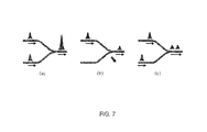
- FIG. 7 (a) Coherent combination of the two-branch inputs; (b) Transmission of a single branch input; (c) Combination of two asynchronously timed pulses, according to an illustrative aspect of the invention.
- FIG. 8 shows: a) A schematic of a multi-wavelength M-tap, first-order pulse-train generator OPTG ⁇ (n) ; (b) A multi-wavelength M-tap, third-order pulse-train generator; (c) A multi-wavelength M-tap, first-order pulse-train modulator, according to illustrative embodiments of the invention.
- a generalized optical pulse train generator embodiment 100 - 1 is shown in FIG. 1 .
- One single optical trigger pulse 102 is divided by multiple delay stages 104 n-1 and coupler stages 106 n to generate multiple sub-pulses 107 .
- the delayed pulse is partially coupled into each coupler stage and dropped at the stage output 108 .
- An output combiner 110 combines the dropped sub-pulses 107 , which appear at different times to form an optical pulse train 112 at the output.
- the timing of the output pulses is determined by the stage delays, while the pulse amplitude is controlled by the coupling coefficients.
- the circuit performs the function of generating multiple optical pulses sequentially from a single trigger pulse, with the timing and amplitude of each pulse determined by circuit design.
- FIG. 2( a ) schematically shows a single wavelength M-tap, first-order pulse-train generator 100 - 2 implemented with ultra-compact microring resonators 106 n as the coupler stages.
- Each coupler stage consists of a microring add-drop filter, which can be either a single ring resonator as shown in FIG. 2( a ) , or higher-order configuration such as the third-order filters illustrated in FIG. 2( b ) .
- All of the microring stages 106 are coupled to the input trigger waveguide 114 in series as shown.
- Optical delay lines are inserted between the stages to introduce a stage (temporal) delay ⁇ .
- the temporal delay value can be different for different stages, based on the circuit application.
- the amplitudes of these M sub-pulses can be controlled by properly adjusting the coupling coefficient of each stage, as known in the art.
- the embodied time-interleaved circuit uses each ring resonator as a compact switch or coupler.
- each ring resonator When there is an input pulse, its power is partially coupled into all of the M stages, circulating in the microrings and dropped at the output of each stage. Therefore, one input pulse will trigger multiple sub-pulses at the output.
- the ultra-compact size of the embodied microring coupler shows advantageously competes with large, conventional directional couplers.
- the embodied circuit may find its application in optical arbitrary waveform generation.
- the time-interleaved approach combines multiple narrow basis pulses, which are generated at a specific sampling time, to form a customized output waveform. Therefore, each stage output in our can be viewed as one basis pulse.
- the final customized output waveform can be generated by modifying the sampling rate and the amplitudes of basis pulses through the control of the stage delay and the coupling coefficient of each stage.
- Arbitrary waveform generation is highly advantageous in high-speed instrumentation and the ultrahigh data rate optical communication field.
- the silicon waveguides and microrings were all built on a SOI platform with 250 nm top silicon and 3 mm buried oxide. Both waveguides and resonators have a cross section of 450 nm ⁇ 250 nm for the single mode operation. As shown in the inset of FIG. 3 , a racetrack resonator configuration was used instead of ring resonator configuration for better coupling control.
- the racetrack was designed to have a radius of 4 mm and a straight coupling length of 3 mm, which corresponded to a ring resonator with an effective radius of 5 mm. All the resonators have the same dimensions and thus resonate at the same frequency.
- the corresponding gaps between the racetrack and input/output waveguides were 160 nm, 140 nm, 120 nm, and 70 nm determined by FDTD simulations.
- coupling coefficients could also be controlled by changing the coupling length in a square-shape ring instead of changing the gaps between rings and waveguides, maintaining the same perimeter of the resonator by adjusting the length of the perpendicular arms. This approach results in a more accurate wavelength and coupling control since small gaps, such as those less than 100 nm, are not easy to control in fabrication.
- the stages behind the first one have a notch at the resonant frequency because most of the input power at that frequency is drained at the first stage.
- equal power coupling could be intuitively achieved by detuning the center frequency of the input pulse off-resonance (blue dash-dot line in FIG. 4( b ) ), so that the power transmission of all the stages in the pulse bandwidth are approximately the same.
- the input pulse was relatively narrow-band; for example, a picosecond modelocked laser diode could be used as the optical source. In our design, we used a 10 ps input pulse around 1550 nm.
- FIG. 5( a ) shows the input pulse evolution in the trigger waveguide (black lines) and corresponding stage outputs (red lines).
- the input pulse propagating in the trigger waveguide becomes progressively smaller since it couples to the microrings and drops a small portion of the pulse at the output of each stage when passing through them.
- the output pulses are almost identical as shown in the black solid line in FIG. 5( b ) .
- the amplitudes of the output pulses are reduced by 6 dB compared to the stage output due to the output power combining loss.
- the through port transfer function was nonzero in the input bandwidth. Therefore, part of the input energy will pass through the network to the through port ((red) dash line in FIG. 5( b ) ), resulting an extra power loss of the whole system. However, this signal may be used as an extra tap in other applications.
- the output waveform exhibited no distortion since dispersion was not considered in our analysis.
- dispersion can be significant in high index contrast SOI waveguides, its impact was relatively small due to the short on-chip traveling distance.
- the material dispersion of silicon is about ⁇ 880 ps/nm-km at 1550 nm
- the pulse broadening is only 30 fs after 10 cm on-chip propagation, which is small compared to the original pulse.
- the anomalous waveguide dispersion can be achieved by tailoring the cross-sectional size of the SOI waveguides, thus compensating the effect of the normal material dispersion and reducing the total dispersion in the waveguides.
- the overall efficiency of the embodied pulse train generator is primarily affected by the waveguide loss and output combiner.
- each stage couples out about 10% of the input pulse energy. Therefore, about 40% input energy is delivered to the four stage outputs.
- the power loss is caused by the assumed 3 dB/cm waveguide propagation loss.
- another 6 dB loss is introduced by the output combiner compared to the stage outputs.
- the overall efficiency of the four-tap prototype is reduced to about 10%, including the through port output. It can be further improved to about 20% if the waveguide loss is reduced to 1 dB/cm.
- FIG. 6 is a FDTD simulation result showing the change of resonant wavelength as the width of the microring changes.
- the slope of the curve is relatively high, which means that a small change in the microring width will significantly affect the resonant frequency.
- a width change of ⁇ 2 nm at 450 nm will result in the wavelength change of 1.6 nm at 1557 nm, which is very large, since the filter bandwidth is only several nanometers.
- the process variation could easily cause the random shift of the resonant peaks, even the split of peaks in the output spectrum of the embodied system.
- FIG. 7( a ) illustrates such an example in a two-branch symmetric Y-junction.
- the output power is the sum of the two input powers, and there should ideally be no power loss.
- FIG. 7( b ) both even and odd modes will be equally excited at the transition region. While the odd mode will convert into the higher order mode and radiate, the output power is only carried by the even mode, which is half of the input power. Therefore, in the instant application ( FIG.
- Another embodiment of the invention is a multi-wavelength optical pulse train generator OPTG ⁇ (n) ) 100 - 3 as illustrated in FIG. 8( a ) .
- M stages resonate at M different frequencies ⁇ M instead of at the same frequency ⁇ as in the single-wavelength OPTG ⁇ (1) .
- the OPTG ⁇ (n) utilizes a broadband input trigger signal, such as ultra-short pulses from a femtosecond fiber laser, whose bandwidth covers all of the M channels. All of the M stages are coupled to the input trigger waveguide in series.
- the input power at the different resonant frequencies is coupled into the corresponding stages, generating pulses with different center frequencies at the stage outputs.
- higher-order (e.g., 3 rd as illustrated) microring add-drop filters which have faster roll-offs, are used to reduce the crosstalk between adjacent stages.
- the output pulses will become wider in the time domain, compared to the input pulse.
- the single-wavelength OPTG ⁇ (1) e.g., FIG.
- delay units are disposed between stages in the input trigger waveguide, which generate a temporal stage delay between the pulses, determining the repetition rate of the output pulse train.
- a single output waveguide 812 rather than an optical combiner 110 (e.g., M-to-1 multi-branch power combiner; see, e.g., FIG. 1 ) can be used to combine all the stage outputs and form the optical pulse train. Because different stage output pulses have different wavelengths, they will not be coupled back into the other stages when passing through them, i.e., there is no “back-coupling” problem. This removes the need to use, e.g., an M-to-1 multi-branch power combiner at the circuit output, eliminating the 10 log 10 M dB power loss caused by asynchronous optical power combination.
Landscapes
- Physics & Mathematics (AREA)
- Nonlinear Science (AREA)
- General Physics & Mathematics (AREA)
- Optics & Photonics (AREA)
- Optical Integrated Circuits (AREA)
- Optical Modulation, Optical Deflection, Nonlinear Optics, Optical Demodulation, Optical Logic Elements (AREA)
Abstract
Description
Claims (14)
Priority Applications (1)
| Application Number | Priority Date | Filing Date | Title |
|---|---|---|---|
| US13/213,612 US9753349B2 (en) | 2010-08-20 | 2011-08-19 | Optical circuit apparatus, method, and application |
Applications Claiming Priority (2)
| Application Number | Priority Date | Filing Date | Title |
|---|---|---|---|
| US37550710P | 2010-08-20 | 2010-08-20 | |
| US13/213,612 US9753349B2 (en) | 2010-08-20 | 2011-08-19 | Optical circuit apparatus, method, and application |
Publications (2)
| Publication Number | Publication Date |
|---|---|
| US20120045163A1 US20120045163A1 (en) | 2012-02-23 |
| US9753349B2 true US9753349B2 (en) | 2017-09-05 |
Family
ID=45594134
Family Applications (1)
| Application Number | Title | Priority Date | Filing Date |
|---|---|---|---|
| US13/213,612 Expired - Fee Related US9753349B2 (en) | 2010-08-20 | 2011-08-19 | Optical circuit apparatus, method, and application |
Country Status (1)
| Country | Link |
|---|---|
| US (1) | US9753349B2 (en) |
Families Citing this family (11)
| Publication number | Priority date | Publication date | Assignee | Title |
|---|---|---|---|---|
| US9164300B2 (en) | 2012-07-02 | 2015-10-20 | Alcatel Lucent | Reconfigurable optical networks |
| CN103609083B (en) * | 2013-05-13 | 2016-08-17 | 华为技术有限公司 | Reception equipment and optical exchange network device |
| JP6266311B2 (en) * | 2013-11-08 | 2018-01-24 | 富士通株式会社 | Optical resonator, optical transmitter and optical resonator control method |
| WO2015100629A1 (en) * | 2013-12-31 | 2015-07-09 | 华为技术有限公司 | Annular optical shifter and optical signal shifting method |
| US10120210B2 (en) | 2016-06-03 | 2018-11-06 | International Business Machines Corporation | Feed-forward optical equalization using an electro-optic modulator with a multi-segment electrode and distributed drivers |
| US10084619B2 (en) | 2016-06-03 | 2018-09-25 | International Business Machines Corporation | Nested feed-forward optical equalization using an electro-optic modulator with a multi-segment electrode |
| JP6998691B2 (en) * | 2017-07-19 | 2022-01-18 | 日本ルメンタム株式会社 | Optical transmission module |
| US10288811B1 (en) * | 2017-12-05 | 2019-05-14 | Hewlett Packard Enterprise Development Lp | Optical switching between waveguides by adjacent resonant structure coupling |
| WO2019207638A1 (en) * | 2018-04-24 | 2019-10-31 | 株式会社大成テクノロジー | Optical phased array and lidar sensor using same |
| US11115130B1 (en) * | 2020-07-09 | 2021-09-07 | Hewlett Packard Enterprise Development Lp | Wavelength control and monitor for dense wavelength division multiplexing (DWDM) silicon photonic receiver |
| US11668874B1 (en) * | 2022-03-21 | 2023-06-06 | Xilinx, Inc. | Optical filter having a tapered profile |
Citations (17)
| Publication number | Priority date | Publication date | Assignee | Title |
|---|---|---|---|---|
| US4652079A (en) * | 1983-08-26 | 1987-03-24 | The Board Of Trustees Of The Leland Stanford Junior University | High speed pulse train generator |
| US4815804A (en) * | 1985-02-08 | 1989-03-28 | The Board Of Trustees Of The Leland Stanford Junior University | In-line fiber optic memory and method of using same |
| US4904041A (en) * | 1988-12-20 | 1990-02-27 | Bell Communications Research, Inc. | Short optical pulse generator having a looped directional coupler external cavity |
| US5572611A (en) * | 1993-06-21 | 1996-11-05 | Nippon Telegraph And Telephone Corporation | Optical signal processor, method of its control, method of its designing, and method of its production |
| US20020061164A1 (en) * | 1999-01-25 | 2002-05-23 | Massachusetts Institute Of Technology, A Massachusetts Corporation | Fast variable optical delay |
| US20020080436A1 (en) * | 2000-12-27 | 2002-06-27 | Hait John N. | Signal-concentrating, photonic, pulse-shaping apparatus and method |
| US20030090767A1 (en) * | 2001-11-15 | 2003-05-15 | Hrl Laboratories, Llc | Agile RF-lightwave waveform synthesis and an optical multi-tone amplitude modulator |
| US20050013538A1 (en) * | 2003-07-18 | 2005-01-20 | Nec Corporation | Tunable dispersion compensator and method for tunable dispersion compensation |
| US6853756B2 (en) * | 2002-03-25 | 2005-02-08 | Helios Photonics, Inc. | Tunable optical waveguide filters with optimized lengths and method of designing same |
| US20050047791A1 (en) * | 2003-08-29 | 2005-03-03 | Tetsuya Miyazaki | Dispersion compensation control method and apparatus thereof and optical transmission method and system thereof |
| US20050196103A1 (en) * | 2004-03-02 | 2005-09-08 | Arkady Kaplan | Integrated loop resonator with adjustable couplings and methods of using the same |
| US20070019900A1 (en) * | 2003-01-29 | 2007-01-25 | Taylor Geoff W | Integrated circuit for programmable optical delay |
| US7245801B2 (en) * | 2002-03-21 | 2007-07-17 | University Of Rochester | Apparatus with a series of resonator structures situated near an optical waveguide for manipulating optical pulses |
| US20090022189A1 (en) * | 2006-01-20 | 2009-01-22 | Toshiaki Okuno | Light Source Apparatus |
| US20090072811A1 (en) * | 2007-05-04 | 2009-03-19 | University Of Rochester | Pulse Measurement Apparatus and Method |
| US20090180786A1 (en) * | 2008-01-11 | 2009-07-16 | Oki Electric Industry Co., Ltd. | Carrier-suppressed optical pulse train generating device and method |
| US7729572B1 (en) * | 2008-07-08 | 2010-06-01 | Hrl Laboratories, Llc | Optical tapped time delay modules and arrays |
-
2011
- 2011-08-19 US US13/213,612 patent/US9753349B2/en not_active Expired - Fee Related
Patent Citations (18)
| Publication number | Priority date | Publication date | Assignee | Title |
|---|---|---|---|---|
| US4652079A (en) * | 1983-08-26 | 1987-03-24 | The Board Of Trustees Of The Leland Stanford Junior University | High speed pulse train generator |
| US4815804A (en) * | 1985-02-08 | 1989-03-28 | The Board Of Trustees Of The Leland Stanford Junior University | In-line fiber optic memory and method of using same |
| US4904041A (en) * | 1988-12-20 | 1990-02-27 | Bell Communications Research, Inc. | Short optical pulse generator having a looped directional coupler external cavity |
| US5572611A (en) * | 1993-06-21 | 1996-11-05 | Nippon Telegraph And Telephone Corporation | Optical signal processor, method of its control, method of its designing, and method of its production |
| US20020061164A1 (en) * | 1999-01-25 | 2002-05-23 | Massachusetts Institute Of Technology, A Massachusetts Corporation | Fast variable optical delay |
| US20020080436A1 (en) * | 2000-12-27 | 2002-06-27 | Hait John N. | Signal-concentrating, photonic, pulse-shaping apparatus and method |
| US20030090767A1 (en) * | 2001-11-15 | 2003-05-15 | Hrl Laboratories, Llc | Agile RF-lightwave waveform synthesis and an optical multi-tone amplitude modulator |
| US7245801B2 (en) * | 2002-03-21 | 2007-07-17 | University Of Rochester | Apparatus with a series of resonator structures situated near an optical waveguide for manipulating optical pulses |
| US6853756B2 (en) * | 2002-03-25 | 2005-02-08 | Helios Photonics, Inc. | Tunable optical waveguide filters with optimized lengths and method of designing same |
| US20070019900A1 (en) * | 2003-01-29 | 2007-01-25 | Taylor Geoff W | Integrated circuit for programmable optical delay |
| US20050013538A1 (en) * | 2003-07-18 | 2005-01-20 | Nec Corporation | Tunable dispersion compensator and method for tunable dispersion compensation |
| US20050047791A1 (en) * | 2003-08-29 | 2005-03-03 | Tetsuya Miyazaki | Dispersion compensation control method and apparatus thereof and optical transmission method and system thereof |
| US20050196103A1 (en) * | 2004-03-02 | 2005-09-08 | Arkady Kaplan | Integrated loop resonator with adjustable couplings and methods of using the same |
| US20090022189A1 (en) * | 2006-01-20 | 2009-01-22 | Toshiaki Okuno | Light Source Apparatus |
| US20090072811A1 (en) * | 2007-05-04 | 2009-03-19 | University Of Rochester | Pulse Measurement Apparatus and Method |
| US20090180786A1 (en) * | 2008-01-11 | 2009-07-16 | Oki Electric Industry Co., Ltd. | Carrier-suppressed optical pulse train generating device and method |
| US20120057882A1 (en) * | 2008-01-11 | 2012-03-08 | Oki Electric Industry Co., Ltd. | Carrier-suppressed optical pulse train generating device |
| US7729572B1 (en) * | 2008-07-08 | 2010-06-01 | Hrl Laboratories, Llc | Optical tapped time delay modules and arrays |
Also Published As
| Publication number | Publication date |
|---|---|
| US20120045163A1 (en) | 2012-02-23 |
Similar Documents
| Publication | Publication Date | Title |
|---|---|---|
| US9753349B2 (en) | Optical circuit apparatus, method, and application | |
| Capmany et al. | Discrete-time optical processing of microwave signals | |
| Wang et al. | Reconfigurable radio-frequency arbitrary waveforms synthesized in a silicon photonic chip | |
| Khan et al. | Ultrabroad-bandwidth arbitrary radiofrequency waveform generation with a silicon photonic chip-based spectral shaper | |
| Chen | Photonic generation of chirped microwave and millimeter wave pulses based on optical spectral shaping and wavelength-to-time mapping in silicon photonics | |
| CN109459816B (en) | Silicon-based optical arbitrary waveform generation chip | |
| Xie et al. | Picosecond optical pulse processing using a terahertz-bandwidth reconfigurable photonic integrated circuit | |
| US8705899B2 (en) | Optical pulse delay generator | |
| Song et al. | Nonlinear distortion in a silicon microring-based electro-optic modulator for analog optical links | |
| Pan et al. | Reflective-type microring resonator for on-chip reconfigurable microwave photonic systems | |
| Zhang et al. | Largely chirped microwave waveform generation using a silicon-based on-chip optical spectral shaper | |
| Tan et al. | RF photonic signal processing with Kerr micro-combs: integration, fractional differentiation and Hilbert transforms | |
| Wang et al. | Integrated optical delay line based on a loopback arrayed waveguide grating for radio-frequency filtering | |
| Samadi et al. | RF arbitrary waveform generation using tunable planar lightwave circuits | |
| Wang et al. | Microring-based optical pulse-train generator | |
| Bui | A review of photonic generation of arbitrary microwave waveforms | |
| Yu et al. | Tunable optical delay line for optical time-division multiplexer | |
| Chan et al. | Single sideband suppressed carrier modulator based frequency shifting recirculating delay line microwave photonic filter | |
| Amiri et al. | TE-like mode analysis of microsystem InGaAsP/InP semiconductor resonator generating 20 GHz repetition rate pulse trains | |
| Adams et al. | RF-arbitrary waveform generation based on microwave photonic filtering | |
| Wang et al. | Integrated High-Repetition-Rate Optical Sampling Chip Exploiting Wavelength and Mode Multiplexing | |
| Ruf et al. | Analysis and design of low-loss and fast all-optical switch elements on silicon nitride for integrated quantum photonics | |
| Liu et al. | On-chip digitally tunable positive/negative dispersion controller using bidirectional chirped multimode waveguide gratings | |
| JP2013257354A (en) | Mode multiplexer/demultiplxer, light transmitter/receiver, and optical communication system | |
| CN112596166A (en) | Optical signal sampling pulse generator based on time-mode interleaving multiplexing |
Legal Events
| Date | Code | Title | Description |
|---|---|---|---|
| AS | Assignment |
Owner name: UNIVERSITY OF ROCHESTER, NEW YORK Free format text: ASSIGNMENT OF ASSIGNORS INTEREST;ASSIGNORS:WU, HUI;WANG, SHANG;REEL/FRAME:026778/0987 Effective date: 20110818 |
|
| AS | Assignment |
Owner name: NATIONAL SCIENCE FOUNDATION, VIRGINIA Free format text: CONFIRMATORY LICENSE;ASSIGNOR:UNIVERSITY OF ROCHESTER;REEL/FRAME:034716/0893 Effective date: 20141205 |
|
| FEPP | Fee payment procedure |
Free format text: PAYOR NUMBER ASSIGNED (ORIGINAL EVENT CODE: ASPN) |
|
| STCF | Information on status: patent grant |
Free format text: PATENTED CASE |
|
| FEPP | Fee payment procedure |
Free format text: MAINTENANCE FEE REMINDER MAILED (ORIGINAL EVENT CODE: REM.); ENTITY STATUS OF PATENT OWNER: SMALL ENTITY |
|
| LAPS | Lapse for failure to pay maintenance fees |
Free format text: PATENT EXPIRED FOR FAILURE TO PAY MAINTENANCE FEES (ORIGINAL EVENT CODE: EXP.); ENTITY STATUS OF PATENT OWNER: SMALL ENTITY |
|
| STCH | Information on status: patent discontinuation |
Free format text: PATENT EXPIRED DUE TO NONPAYMENT OF MAINTENANCE FEES UNDER 37 CFR 1.362 |
|
| FP | Lapsed due to failure to pay maintenance fee |
Effective date: 20210905 |