US9723668B2 - Switching converter and lighting device using the same - Google Patents
Switching converter and lighting device using the same Download PDFInfo
- Publication number
- US9723668B2 US9723668B2 US15/172,776 US201615172776A US9723668B2 US 9723668 B2 US9723668 B2 US 9723668B2 US 201615172776 A US201615172776 A US 201615172776A US 9723668 B2 US9723668 B2 US 9723668B2
- Authority
- US
- United States
- Prior art keywords
- capacitor
- circuit
- voltage
- switching
- switching converter
- Prior art date
- Legal status (The legal status is an assumption and is not a legal conclusion. Google has not performed a legal analysis and makes no representation as to the accuracy of the status listed.)
- Active
Links
Images


Classifications
-
- H05B33/0815—
-
- H—ELECTRICITY
- H02—GENERATION; CONVERSION OR DISTRIBUTION OF ELECTRIC POWER
- H02M—APPARATUS FOR CONVERSION BETWEEN AC AND AC, BETWEEN AC AND DC, OR BETWEEN DC AND DC, AND FOR USE WITH MAINS OR SIMILAR POWER SUPPLY SYSTEMS; CONVERSION OF DC OR AC INPUT POWER INTO SURGE OUTPUT POWER; CONTROL OR REGULATION THEREOF
- H02M1/00—Details of apparatus for conversion
- H02M1/32—Means for protecting converters other than automatic disconnection
-
- H—ELECTRICITY
- H02—GENERATION; CONVERSION OR DISTRIBUTION OF ELECTRIC POWER
- H02M—APPARATUS FOR CONVERSION BETWEEN AC AND AC, BETWEEN AC AND DC, OR BETWEEN DC AND DC, AND FOR USE WITH MAINS OR SIMILAR POWER SUPPLY SYSTEMS; CONVERSION OF DC OR AC INPUT POWER INTO SURGE OUTPUT POWER; CONTROL OR REGULATION THEREOF
- H02M3/00—Conversion of dc power input into dc power output
- H02M3/02—Conversion of dc power input into dc power output without intermediate conversion into ac
- H02M3/04—Conversion of dc power input into dc power output without intermediate conversion into ac by static converters
- H02M3/10—Conversion of dc power input into dc power output without intermediate conversion into ac by static converters using discharge tubes with control electrode or semiconductor devices with control electrode
- H02M3/145—Conversion of dc power input into dc power output without intermediate conversion into ac by static converters using discharge tubes with control electrode or semiconductor devices with control electrode using devices of a triode or transistor type requiring continuous application of a control signal
- H02M3/155—Conversion of dc power input into dc power output without intermediate conversion into ac by static converters using discharge tubes with control electrode or semiconductor devices with control electrode using devices of a triode or transistor type requiring continuous application of a control signal using semiconductor devices only
- H02M3/156—Conversion of dc power input into dc power output without intermediate conversion into ac by static converters using discharge tubes with control electrode or semiconductor devices with control electrode using devices of a triode or transistor type requiring continuous application of a control signal using semiconductor devices only with automatic control of output voltage or current, e.g. switching regulators
-
- H05B33/0803—
-
- H—ELECTRICITY
- H05—ELECTRIC TECHNIQUES NOT OTHERWISE PROVIDED FOR
- H05B—ELECTRIC HEATING; ELECTRIC LIGHT SOURCES NOT OTHERWISE PROVIDED FOR; CIRCUIT ARRANGEMENTS FOR ELECTRIC LIGHT SOURCES, IN GENERAL
- H05B45/00—Circuit arrangements for operating light-emitting diodes [LED]
-
- H—ELECTRICITY
- H05—ELECTRIC TECHNIQUES NOT OTHERWISE PROVIDED FOR
- H05B—ELECTRIC HEATING; ELECTRIC LIGHT SOURCES NOT OTHERWISE PROVIDED FOR; CIRCUIT ARRANGEMENTS FOR ELECTRIC LIGHT SOURCES, IN GENERAL
- H05B45/00—Circuit arrangements for operating light-emitting diodes [LED]
- H05B45/30—Driver circuits
- H05B45/37—Converter circuits
- H05B45/3725—Switched mode power supply [SMPS]
- H05B45/375—Switched mode power supply [SMPS] using buck topology
-
- H—ELECTRICITY
- H05—ELECTRIC TECHNIQUES NOT OTHERWISE PROVIDED FOR
- H05B—ELECTRIC HEATING; ELECTRIC LIGHT SOURCES NOT OTHERWISE PROVIDED FOR; CIRCUIT ARRANGEMENTS FOR ELECTRIC LIGHT SOURCES, IN GENERAL
- H05B45/00—Circuit arrangements for operating light-emitting diodes [LED]
- H05B45/30—Driver circuits
- H05B45/37—Converter circuits
- H05B45/3725—Switched mode power supply [SMPS]
- H05B45/38—Switched mode power supply [SMPS] using boost topology
-
- H—ELECTRICITY
- H05—ELECTRIC TECHNIQUES NOT OTHERWISE PROVIDED FOR
- H05B—ELECTRIC HEATING; ELECTRIC LIGHT SOURCES NOT OTHERWISE PROVIDED FOR; CIRCUIT ARRANGEMENTS FOR ELECTRIC LIGHT SOURCES, IN GENERAL
- H05B45/00—Circuit arrangements for operating light-emitting diodes [LED]
- H05B45/30—Driver circuits
- H05B45/37—Converter circuits
- H05B45/3725—Switched mode power supply [SMPS]
- H05B45/385—Switched mode power supply [SMPS] using flyback topology
-
- Y—GENERAL TAGGING OF NEW TECHNOLOGICAL DEVELOPMENTS; GENERAL TAGGING OF CROSS-SECTIONAL TECHNOLOGIES SPANNING OVER SEVERAL SECTIONS OF THE IPC; TECHNICAL SUBJECTS COVERED BY FORMER USPC CROSS-REFERENCE ART COLLECTIONS [XRACs] AND DIGESTS
- Y02—TECHNOLOGIES OR APPLICATIONS FOR MITIGATION OR ADAPTATION AGAINST CLIMATE CHANGE
- Y02B—CLIMATE CHANGE MITIGATION TECHNOLOGIES RELATED TO BUILDINGS, e.g. HOUSING, HOUSE APPLIANCES OR RELATED END-USER APPLICATIONS
- Y02B20/00—Energy efficient lighting technologies, e.g. halogen lamps or gas discharge lamps
- Y02B20/30—Semiconductor lamps, e.g. solid state lamps [SSL] light emitting diodes [LED] or organic LED [OLED]
Definitions
- the present disclosure relates to a switching converter.
- FIG. 1 is a block diagram of a lighting device including an LED.
- a lighting device 500 r includes an LED light source 502 , a rectifying circuit 504 , a smoothing condenser 506 , and a switching converter 100 r .
- the LED light source 502 is an LED string, and includes a plurality of LEDs connected in series.
- the rectifying circuit 504 and the smoothing condenser 506 rectify and smooth a commercial alternating current (AC) voltage V AC to convert it into a DC voltage V DC .
- the switching converter 100 r receives the DC voltage V DC as an input voltage V IN and supplies a driving current I LED corresponding to a desired amount of light to the LED light source 502 .
- AC alternating current
- the switching converter 100 r is a step-down converter, and includes an output circuit 102 and a control circuit 200 r .
- the output circuit 102 includes a smoothing capacitor C 1 , a rectifying diode D 1 , a switching transistor M 1 , an inductor L 1 , a detection resistor R CS , a capacitor C 11 , and resistors R 11 and R 12 .
- a coil current I L1 flows to the detection resistor R CS by way of the inductor L 1 and the switching transistor M 1 .
- a voltage drop (current detection signal) V CS of the detection resistor R CS is fed back to a current detection (CS) terminal of the control circuit 200 r .
- the control circuit 200 r generates a pulse signal whose duty ratio is adjusted such that a peak of the current detection signal V CS becomes close to a target voltage corresponding to a target amount of light of the LED light source 502 , and switches the switching transistor M 1 connected to an OUT terminal.
- a driving current I LED smoothed from the coil current I L1 is supplied to the LED light source 502 .
- a voltage V ZT that is based on a drain voltage V D of the switching transistor M 1 is input to a zero cross detection (ZT) terminal of the control circuit 200 r through the capacitor C 11 and the resistors R 11 and R 12 .
- the control circuit 200 r detects that the coil current I L flowing through the inductor L 1 becomes zero (zero cross) according to the voltage V ZT , and turns on the switching transistor M 1 . Further, the control circuit 200 r detects that the current detection signal V CS reaches a target voltage V REF , and turns off the switching transistor M 1 .
- a DC voltage V DC is input to a high voltage (VH) terminal of the control circuit 200 r , and a capacitor C 21 is connected to a power source (VCC) terminal.
- the control circuit 200 r includes a start-up circuit 202 installed between the VH terminal and the VCC terminal. Since the DC voltage V DC is a high voltage of 100V or higher, the start-up circuit 202 is configured by using a high withstand voltage device.
- the control circuit 200 r is started up.
- a start-up current flows from the VH terminal to the capacitor C 21 by way of the start-up circuit 202 and the VCC terminal so that the capacitor C 21 is charged.
- a voltage V CC of the capacitor C 21 is a power source voltage of the control circuit 200 r .
- the control circuit 200 r is operable when the power source voltage V CC exceeds a predetermined threshold voltage (lowest operating voltage) V UVLO , and starts to switch the switching transistor M 1 .
- V UVLO lowest operating voltage
- the present inventors reviewed the switching converter 100 r of FIG. 1 and recognized the following technical problem.
- a user may want to set up a time (start-up time) for the LED light source 502 to actually be lighted at a desirable time after the user turns on the power.
- a fluorescent lamp or an incandescent lamp is lighted through a start-up time which is relatively long until it is lighted after a switch is turned on, but a start-up time of a semiconductor light source such as the LED light source 502 is shorter than that of the fluorescent lamp or the incandescent lamp, and the use of the LED light source 502 in combination with the fluorescent lamp or the incandescent lamp causes disharmony. Further, even when the LED light source 502 is used alone, it may be desirable that the start-up time of the LED light source 502 is relatively long.
- the lighting device 500 r having the LED light source 502 has been described as an example, but a start-up time taken from a time at which power is applied to a time at which a load is operated may be set, even for the switching converter 100 r for supplying power to a certain load in applications other than the lighting device 500 r.
- the present disclosure provides some embodiments of a switching converter in which a start-up time may be set.
- a switching converter for supplying power to a load.
- the switching converter includes: an output circuit including at least a switching transistor, an inductive element, and a rectifying element configured to rectify a current flowing to the inductive element according to switching of the switching transistor; a control circuit configured to drive the switching transistor; a first capacitor configured to generate a power source voltage for the control circuit between both ends of the first capacitor; a start-up circuit installed between an input line to the switching converter and the first capacitor and configured to charge the first capacitor with an input voltage of the input line; and a discharge circuit configured to discharge the first capacitor when the switching converter is started up.
- the first capacitor is charged with a difference between a charge current provided by the start-up circuit and a discharge current provided by the discharge circuit.
- a charge speed by adjusting the discharge current provided by the discharge circuit, and further set a rising time of the power source voltage and a start-up time of the switching converter.
- a discharge current flowing through the discharge circuit may be increased after the switching converter is started up, and subsequently decreased over time.
- the discharge circuit may include a second capacitor charged according to the input voltage, and the discharge current flowing through the discharge circuit may decrease as a voltage of the second capacitor increases.
- the discharge circuit may include: a discharge transistor installed in parallel to the first capacitor; and a bias circuit configured to supply a bias signal that is based on the input voltage to a control terminal of the discharge transistor.
- the bias circuit may include: a second capacitor; and a first resistor installed between the input line and the second capacitor.
- the bias signal that is based on a voltage of the second capacitor may be supplied to the control terminal of the discharge transistor.
- the bias circuit may further include a second resistor installed in parallel to the second capacitor.
- the bias circuit may further include a Zener diode installed in series to the first resistor between the second capacitor and the input line.
- the discharge transistor may be a PNP-type bipolar transistor or a P-channel MOSFET.
- control circuit may include: a power source terminal to which the first capacitor is connected; and a high voltage terminal configured to receive the input voltage from the input line.
- the control circuit may include the start-up circuit incorporated between the power source terminal and the high voltage terminal.
- the start-up circuit may include a third resistor installed outside the control circuit between the input line and the first capacitor.
- the start-up circuit having a high withstand voltage device is not required in the control circuit.
- the load may be a semiconductor light source.
- the load may be a semiconductor light source.
- the output circuit may include: an output capacitor installed between an output line to which one end of the load is connected and the input line; a diode having a cathode connected to the input line; an inductor installed between the output line and an anode of the diode; and the switching transistor installed between the anode of the diode and a ground.
- the output circuit may have a flyback-type topology. In some embodiments, the output circuit may have a topology of a buck converter or a boost converter.
- the lighting device may include: a semiconductor light source; and any one of the switching converters described above, configured to light the semiconductor light source.
- the lighting device may further include: a rectifying circuit configured to rectify an AC voltage; and a smoothing capacitor configured to smooth an output voltage of the rectifying circuit to supply the same to an input line of the switching converter.
- any combinations of the foregoing components or replacement of expressions among a method, an apparatus, a system and the like are also effective as embodiments of the present disclosure.
- FIG. 1 is a block diagram of a lighting device including an LED.
- FIG. 2 is a circuit diagram of a lighting device including a switching converter according to an embodiment of the present disclosure.
- FIG. 3 is an operational waveform view when the switching converter of FIG. 1 is started up.
- FIG. 4 is a circuit diagram illustrating a configuration example of a discharge circuit.
- FIG. 5 is a circuit diagram illustrating a configuration example of a discharge circuit.
- FIG. 6 is a circuit diagram illustrating a specific configuration example of the discharge circuit.
- FIG. 7 is a circuit diagram of a switching converter according to a first modification of the present disclosure.
- FIG. 8 is a circuit diagram of a switching converter according to a fourth modification of the present disclosure.
- FIGS. 9A to 9C are views illustrating specific examples of the lighting device.
- a state where a member A is connected to a member B includes a case where the member A and the member B are physically directly connected or even a case in which the member A and the member B are indirectly connected through any other member that does not affect an electrical connection state thereof.
- a state where a member C is installed between a member A and a member B also includes a case where the member A and the member C or the member B and the member C are indirectly connected through any other member that does not affect an electrical connection state, in addition to a case in which the member A and the member C or the member B and the member C are directly connected.
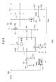
- FIG. 2 is a circuit diagram of a lighting device 500 including a switching converter 100 according to an embodiment of the present disclosure.
- the lighting device 500 includes an LED light source 502 , a rectifying circuit 504 , a smoothing condenser 506 , and a switching converter 100 .
- a basic configuration of the lighting device 500 is the same as that described with reference to FIG. 1 .
- a filter may be inserted in a front stage or a rear stage of the smoothing condenser 506 .
- the switching converter 100 Upon receipt of a DC input voltage V DC by an input line 104 , the switching converter 100 generates an output voltage V OUT by converting the DC input voltage V DC to have an appropriate voltage level, and supplies the output voltage V OUT to a load connected to an output line 106 .
- the load is a semiconductor light source, and for example, the load is the LED light source 502 including a plurality of LEDs connected in series.
- the switching converter 100 stabilizes a driving current I LED flowing through the LED light source 502 to a target current I REF corresponding to a target luminance of the LED light source 502 through a feedback controlling.
- the switching converter 100 includes an output circuit 102 , a control circuit 200 , a first capacitor C 21 , and a discharge circuit 110 .
- the output circuit 102 includes at least a switching transistor M 1 , an inductor L 1 as an inductive element, and a rectifying diode D 1 as a rectifying device for rectifying a current flowing through the inductor L 1 according to switching of the switching transistor M 1 .
- the switching transistor M 1 may be incorporated in the control circuit 200 .
- the topology of the output circuit 102 is not particularly limited, and an appropriate circuit configuration may be employed according to a relationship between the input voltage V DC and the output voltage V OUT and a switching scheme of the switching transistor M 1 .
- the control circuit 200 feedback-controls a time ratio (duty ratio) of a switching ON time and a switching OFF time of the switching transistor M 1 such that the driving current I LED becomes close to the target current I REF . Since a commercial product may be used as the control circuit 200 , a description of an internal configuration thereof will be omitted.
- the switching converter 100 is a buck converter (or a step-down converter), and the output circuit 102 includes the inductor L 1 , the rectifying diode D 1 , the switching transistor M 1 , a detection resistor R CS , a smoothing capacitor C 1 , a capacitor C 11 , and resistors R 11 and R 12 .
- the driving current I LED which passes through the input line 104 , the LED light source 502 , the inductor L 1 , and the switching transistor M 1 flows to the detection resistor R CS .
- the driving current I LED flows along a path of the input line 104 , the LED light source 502 , the inductor L 1 , and the rectifying diode D 1 .
- a voltage drop (current detection signal) V CS in proportion to a coil current I L1 is generated across the detection resistor R CS .
- the current detection signal V CS is fed back to the current detection (CS) terminal of the control circuit 200 .
- the control circuit 200 generates a pulse signal whose duty ratio is adjusted such that a peak of the current detection signal V CS becomes close to the target voltage V REF corresponding to the target current I REF , and switches the switching transistor M 1 connected to the OUT terminal.
- the control circuit 200 switches the switching transistor M 1 according to a so-called quasi-resonant (QR) scheme.
- QR quasi-resonant
- a detection voltage V ZT that is based on a drain voltage V D of the switching transistor M 1 is input to the zero cross detection (ZT) terminal of the control circuit 200 through the capacitor C 11 and the resistors R 11 and R 12 .
- the detection voltage V ZT has a voltage level corresponding to a coil current I L of the inductor L 1 during an OFF period of the switching transistor M 1 .
- the control circuit 200 detects that the coil current I L flowing through the inductor L 1 becomes zero (zero cross) according to the detection voltage V ZT , and turns on the switching transistor M 1 . Further, the control circuit 200 detects that the current detection signal V CS reaches the target voltage V REF , and turns off the switching transistor M 1 .
- the first capacitor C 21 generates a power source voltage V CC between both ends of the first capacitor C 21 .
- the power source voltage V CC is connected to a power source (VCC) terminal of the control circuit 200 .
- the control circuit 200 operates using the power source voltage V CC as a power source.
- the DC voltage V DC is input to the high voltage (VH) terminal of the control circuit 200 .
- the control circuit 200 includes a start-up circuit 202 installed between the VH terminal and the VCC terminal. Since the DC voltage V DC has a high voltage of 100V or higher, the start-up circuit 202 is configured by using a high withstand voltage device.
- the start-up circuit 202 is installed between the input line 104 to the switching converter 100 and the first capacitor C 21 , receives the input voltage V DC of the input line 104 , and supplies a charge current I CHG to the first capacitor C 21 to charge the first capacitor C 21 .
- the discharge circuit 110 starts discharging of the first capacitor C 21 with a rise of the input voltage V DC of the input line 104 when the switching converter 100 is started up.
- a discharge current I DIS flowing through the discharge circuit 110 is increased to its peak after the switching converter 100 is started up, and subsequently decreased over time.
- the discharge circuit 110 may be recognized as a variable current source.
- FIG. 3 is an operational waveform view when the switching converter 100 of FIG. 1 is started up.
- the vertical axis and horizontal axis of the waveform views or time charts herein are appropriately scaled up and down to facilitate understanding, and also, respective waveforms illustrated are simplified, exaggerated, or emphasized to facilitate understanding.
- an AC voltage V AC is supplied to the LED light source 502 .
- a DC input voltage V DC is generated on the input line 104 of the switching converter 100 .
- the charge current I CHG flows from the input line 104 to the first capacitor C 21 through the start-up circuit 202 .
- the discharge current I DIS flows out from the first capacitor C 21 through the discharge circuit 110 .
- the first capacitor C 21 is charged by a current I C21 corresponding to a difference between the charge current I CHG and the discharge current I DIS .
- the power source voltage V CC is increased.
- the control circuit 200 starts to switch the switching transistor M 1 to light the LED light source 502 .
- a start-up time T START of the switching converter 100 corresponds to a period of times t 0 to t 1 .
- the operation of the switching converter 100 according to the embodiment has been described above.
- the operation of the switching converter 100 r of FIG. 1 is illustrated by the alternate long and short dash line in FIG. 3 .
- the first capacitor C 21 is charged with a large current after start-up, and the power source voltage V CC is increased within a short time and a start up time T START ′ is shortened.
- the start-up time T START can be lengthened, when compared with the related art. Further, it is possible to set the start-up time T START according to an amount of current of the discharge current I DIS generated by the discharge circuit 110 .
- Setting the start-up time T START refers to setting a lighting time of the LED light source 502 .
- a related-art fluorescent lamp or an incandescent lamp is lighted after a start-up time elapses which is relatively long from a time at which a switch is turned on to a time at which the fluorescent lamp or the incandescent lamp is lighted.
- the switching converter 100 of the embodiment it is possible to realize a lighting time comparable to that of the fluorescent lamp or the incandescent lamp.
- the present disclosure is recognized through the block diagram and circuit diagram of FIG. 2 , and encompasses various devices and circuits derived from the above description and is not limited to a specific configuration.
- a more specific configuration example will be described in order to help and clarify understanding of the essence and circuitry operation of the present disclosure, rather than to narrow the scope of the present disclosure.
- FIG. 4 is a circuit diagram illustrating a configuration example of the discharge circuit 110 .
- the discharge circuit 110 includes a discharge transistor 112 and a bias circuit 114 .
- the discharge transistor 112 is installed in parallel to the first capacitor C 21 .
- the bias circuit 114 supplies a bias signal S 21 to a control terminal (base or gate) of the discharge transistor 112 .
- the bias circuit 114 starts to generate the bias signal S 21 .
- the discharge transistor 112 may be configured as, for example, a PNP-type bipolar transistor or a P-channel MOSFET.
- the bias circuit 114 increases the bias signal S 21 toward a predetermined voltage level over time.
- the discharge current I DIS flowing through the discharge transistor 112 is increased to its peak immediately after the start-up, and subsequently decreased over time.
- FIG. 5 is a circuit diagram illustrating a configuration example of the discharge circuit 110 .
- the discharge circuit 110 includes a second capacitor C 22 , a variable current source 116 , and a charge circuit 118 .
- the charge circuit 118 charges the second capacitor C 22 to a predetermined voltage level. In other words, the second capacitor C 22 is charged according to the input voltage V DC .
- variable current source 116 Upon receipt of a voltage V C22 generated in the second capacitor C 22 , the variable current source 116 generates a discharge current I DIS corresponding to the voltage V C22 .
- the variable current source 116 may be recognized as a V/I conversion circuit.
- the discharge current I DIS is decreased as the voltage V C22 of the second capacitor C 22 is increased.
- the discharge circuit 110 of FIG. 4 and the discharge circuit 110 of FIG. 5 may be understood to be the same circuit but recognized in different aspects.
- the discharge transistor 112 of FIG. 4 may correspond to the variable current source 116 of FIG. 5
- the bias signal S 21 of FIG. 4 may correspond to the voltage V C22 of FIG. 5
- the bias circuit 114 of FIG. 4 may correspond to the charge circuit 118 and the second capacitor C 22 of FIG. 5 .
- FIG. 6 is a circuit diagram illustrating a specific configuration example of the discharge circuit 110 .
- the charge circuit 118 includes a first resistor R 21 , a second resistor R 22 , and a Zener diode ZD 1 .
- the first resistor R 21 is installed between the input line 104 and the second capacitor C 22 .
- the second resistor R 22 is installed in parallel to the second capacitor C 22 .
- the Zener diode ZD 1 is installed in series to the first resistor R 21 between the second capacitor C 22 and the input line 104 .
- the variable current source 116 may include a diode D 21 connected to the base of the discharge transistor 112 .
- the voltage V C22 is varied according to a CR time constant corresponding to the second capacitor C 22 and the first resistor R 21 .
- a start-up time according to a capacitance value and a resistance value.
- FIG. 7 is a circuit diagram of a switching converter 100 a according to a first modification.
- a start-up circuit 202 a includes a third resistor R 23 externally attached to the control circuit 200 .
- the third resistor R 23 is installed between the input line 104 and the first capacitor C 21 .
- the start-up circuit 202 a includes a Zener diode (not shown) connected in series to the third resistor R 23 .
- an auxiliary winding coupled to the inductor L 1 may be installed, instead of the capacitor C 11 and the resistors R 11 and R 12 , to input a V ZT corresponding to a voltage generated at the auxiliary winding to the ZT terminal of the control circuit 200 . Further, with this configuration, it is possible to realize a pseudo-resonance mode.
- the control scheme of the switching converter 100 is not limited to the pseudo-resonance scheme, and a hysteresis control (Bang-Bang control), a PWM control (or PFM control) of a voltage mode, a PWM control (or PFM control) of a current mode, or the like may be employed.
- FIG. 8 is a circuit diagram of a switching converter 100 b according to a fourth modification.
- an output circuit 102 b has a flyback type topology and includes a transformer T 1 , a diode D 1 , a smoothing capacitor C 1 , resistors R 31 and R 32 , a shunt regulator 120 , and a photocoupler 122 .
- the control circuit 200 b is a controller of a flyback converter, and a commercial product may be used.
- An output voltage V OUT _ S divided by the resistors R 31 and R 32 is input to an REF terminal of the shunt regulator 120 .
- the shunt regulator 120 generates a current I ERR corresponding to an error between the voltage V OUT _ S and the reference voltage V REF , and drives a light emitting device of the photocoupler 122 .
- a feedback current I FB corresponding to the output voltage V OUT _ S flows to a light receiving device of the photocoupler 122 .
- a feedback voltage V FB corresponding to the feedback current I FB is generated at the FB terminal.
- the control circuit 200 b drives the switching transistor M 1 with a duty ratio corresponding to the feedback voltage V FB .
- the control circuit 200 b includes a VH terminal, a VCC terminal, and a start-up circuit 202 .
- the discharge circuit 110 discharges the first capacitor C 21 .
- a diode D 2 and an auxiliary winding W 3 of the transformer T 1 are connected to the first capacitor C 21 .
- the control circuit 200 b can be operated after the lapse of a start-up time T START .
- the control circuit 200 b When the control circuit 200 b is operable and the switching transistor M 1 is started to be switched, the voltage V CC of the first capacitor C 21 is stabilized to a predetermined voltage in proportion to the output voltage V OUT by a converter including the auxiliary winding W 3 and the diode D 2 .
- the switching converter 100 b of FIG. 8 may be appropriately used in an AC/DC converter, an AC adapter, or the like.
- the switching converter 100 may be a buck converter or a boost converter, and the topology of the output circuit 102 may be determined according to the type of the converter. Further, a synchronous rectification type, rather than a diode rectification type, may be used.
- the type of the load is not particularly limited
- FIGS. 9A to 9C are views illustrating specific examples of the lighting device 500 .
- a lighting device 500 a of FIG. 9A is a tubular LED lighting.
- a plurality of LED devices constituting an LED string as the LED light source 502 are laid out on a board 510 .
- a rectifying circuit 504 , a control circuit 200 , an output circuit 102 , and the like are mounted on the board 510 .
- a lighting device 500 b of FIG. 9B is a bulb-type LED lighting.
- An LED module as the LED light source 502 is mounted on a board 510 .
- a control circuit 200 and a rectifying circuit 504 are mounted within the housing of the lighting device 500 b.
- a lighting device 500 c of FIG. 9C is a backlight incorporated in a liquid crystal display (LCD) 600 .
- the lighting device 500 c irradiates the rear of a liquid crystal panel 602 .
- the lighting device 500 may be used for ceiling lights. In this manner, the lighting device 500 may be used for various applications.
Landscapes
- Engineering & Computer Science (AREA)
- Power Engineering (AREA)
- Circuit Arrangement For Electric Light Sources In General (AREA)
- Led Devices (AREA)
- Dc-Dc Converters (AREA)
Abstract
A switching converter for supplying power to a load, includes: an output circuit including at least a switching transistor, an inductive element, and a rectifying element configured to rectify a current flowing to the inductive element according to switching of the switching transistor; a control circuit configured to drive the switching transistor; a first capacitor configured to generate a power source voltage for the control circuit between both ends of the first capacitor; a start-up circuit installed between an input line to the switching converter and the first capacitor and configured to charge the first capacitor with an input voltage of the input line; and a discharge circuit configured to discharge the first capacitor when the switching converter is started up.
Description
This application is based upon and claims the benefit of priority from Japanese Patent Application No. 2015-114677, filed on Jun. 5, 2015, the entire contents of which are incorporated herein by reference.
The present disclosure relates to a switching converter.
Semiconductor light sources such as light emitting diodes (LEDs) as a liquid crystal backlight or lighting equipment have become prevalent. FIG. 1 is a block diagram of a lighting device including an LED. A lighting device 500 r includes an LED light source 502, a rectifying circuit 504, a smoothing condenser 506, and a switching converter 100 r. The LED light source 502 is an LED string, and includes a plurality of LEDs connected in series. The rectifying circuit 504 and the smoothing condenser 506 rectify and smooth a commercial alternating current (AC) voltage VAC to convert it into a DC voltage VDC. The switching converter 100 r receives the DC voltage VDC as an input voltage VIN and supplies a driving current ILED corresponding to a desired amount of light to the LED light source 502.
The switching converter 100 r is a step-down converter, and includes an output circuit 102 and a control circuit 200 r. The output circuit 102 includes a smoothing capacitor C1, a rectifying diode D1, a switching transistor M1, an inductor L1, a detection resistor RCS, a capacitor C11, and resistors R11 and R12.
During an ON period of the switching transistor M1, a coil current IL1 flows to the detection resistor RCS by way of the inductor L1 and the switching transistor M1. A voltage drop (current detection signal) VCS of the detection resistor RCS is fed back to a current detection (CS) terminal of the control circuit 200 r. The control circuit 200 r generates a pulse signal whose duty ratio is adjusted such that a peak of the current detection signal VCS becomes close to a target voltage corresponding to a target amount of light of the LED light source 502, and switches the switching transistor M1 connected to an OUT terminal. A driving current ILED smoothed from the coil current IL1 is supplied to the LED light source 502.
A voltage VZT that is based on a drain voltage VD of the switching transistor M1 is input to a zero cross detection (ZT) terminal of the control circuit 200 r through the capacitor C11 and the resistors R11 and R12. The control circuit 200 r detects that the coil current IL flowing through the inductor L1 becomes zero (zero cross) according to the voltage VZT, and turns on the switching transistor M1. Further, the control circuit 200 r detects that the current detection signal VCS reaches a target voltage VREF, and turns off the switching transistor M1.
A DC voltage VDC is input to a high voltage (VH) terminal of the control circuit 200 r, and a capacitor C21 is connected to a power source (VCC) terminal. The control circuit 200 r includes a start-up circuit 202 installed between the VH terminal and the VCC terminal. Since the DC voltage VDC is a high voltage of 100V or higher, the start-up circuit 202 is configured by using a high withstand voltage device.
When a user of the lighting device 500 r turns on a switch for lighting on and off the lighting device 500 r, the AC voltage VAC is supplied to the rectifying circuit 504 and the voltage VDC of the smoothing condenser 506 is increased. In response to turning on the switch, the control circuit 200 r is started up. When the control circuit is started up, a start-up current flows from the VH terminal to the capacitor C21 by way of the start-up circuit 202 and the VCC terminal so that the capacitor C21 is charged.
A voltage VCC of the capacitor C21 is a power source voltage of the control circuit 200 r. The control circuit 200 r is operable when the power source voltage VCC exceeds a predetermined threshold voltage (lowest operating voltage) VUVLO, and starts to switch the switching transistor M1. Thus, the LED light source 502 is lighted.
The present inventors reviewed the switching converter 100 r of FIG. 1 and recognized the following technical problem.
A user may want to set up a time (start-up time) for the LED light source 502 to actually be lighted at a desirable time after the user turns on the power. In a related-art, a fluorescent lamp or an incandescent lamp is lighted through a start-up time which is relatively long until it is lighted after a switch is turned on, but a start-up time of a semiconductor light source such as the LED light source 502 is shorter than that of the fluorescent lamp or the incandescent lamp, and the use of the LED light source 502 in combination with the fluorescent lamp or the incandescent lamp causes disharmony. Further, even when the LED light source 502 is used alone, it may be desirable that the start-up time of the LED light source 502 is relatively long.
Here, in order to clarify the technical problem, the lighting device 500 r having the LED light source 502 has been described as an example, but a start-up time taken from a time at which power is applied to a time at which a load is operated may be set, even for the switching converter 100 r for supplying power to a certain load in applications other than the lighting device 500 r.
The present disclosure provides some embodiments of a switching converter in which a start-up time may be set.
According to one embodiment of the present disclosure, there is provided a switching converter for supplying power to a load. The switching converter includes: an output circuit including at least a switching transistor, an inductive element, and a rectifying element configured to rectify a current flowing to the inductive element according to switching of the switching transistor; a control circuit configured to drive the switching transistor; a first capacitor configured to generate a power source voltage for the control circuit between both ends of the first capacitor; a start-up circuit installed between an input line to the switching converter and the first capacitor and configured to charge the first capacitor with an input voltage of the input line; and a discharge circuit configured to discharge the first capacitor when the switching converter is started up.
The first capacitor is charged with a difference between a charge current provided by the start-up circuit and a discharge current provided by the discharge circuit. Thus, it is possible to adjust a charge speed by adjusting the discharge current provided by the discharge circuit, and further set a rising time of the power source voltage and a start-up time of the switching converter.
A discharge current flowing through the discharge circuit may be increased after the switching converter is started up, and subsequently decreased over time.
The discharge circuit may include a second capacitor charged according to the input voltage, and the discharge current flowing through the discharge circuit may decrease as a voltage of the second capacitor increases.
The discharge circuit may include: a discharge transistor installed in parallel to the first capacitor; and a bias circuit configured to supply a bias signal that is based on the input voltage to a control terminal of the discharge transistor.
Thus, it is possible to change the discharge current flowing through the discharge transistor according to the input voltage.
In some embodiments, the bias circuit may include: a second capacitor; and a first resistor installed between the input line and the second capacitor. The bias signal that is based on a voltage of the second capacitor may be supplied to the control terminal of the discharge transistor.
Since a voltage of the control terminal of the discharge transistor is increased according to a CR time constant, it is possible to adjust the start-up time based on capacitance of the second capacitor and a resistance value of the first resistor.
In some embodiments, the bias circuit may further include a second resistor installed in parallel to the second capacitor.
In some embodiments, the bias circuit may further include a Zener diode installed in series to the first resistor between the second capacitor and the input line.
In some embodiments, the discharge transistor may be a PNP-type bipolar transistor or a P-channel MOSFET.
In some embodiments, the control circuit may include: a power source terminal to which the first capacitor is connected; and a high voltage terminal configured to receive the input voltage from the input line. The control circuit may include the start-up circuit incorporated between the power source terminal and the high voltage terminal.
In some embodiments, the start-up circuit may include a third resistor installed outside the control circuit between the input line and the first capacitor.
In this case, the start-up circuit having a high withstand voltage device is not required in the control circuit.
In some embodiments, the load may be a semiconductor light source. Thus, it is possible to set a lighting time of the semiconductor light source.
In some embodiments, the output circuit may include: an output capacitor installed between an output line to which one end of the load is connected and the input line; a diode having a cathode connected to the input line; an inductor installed between the output line and an anode of the diode; and the switching transistor installed between the anode of the diode and a ground.
In some embodiments, the output circuit may have a flyback-type topology. In some embodiments, the output circuit may have a topology of a buck converter or a boost converter.
According to another embodiment of the present disclosure, there is provided a lighting device. The lighting device may include: a semiconductor light source; and any one of the switching converters described above, configured to light the semiconductor light source.
In some embodiments, the lighting device may further include: a rectifying circuit configured to rectify an AC voltage; and a smoothing capacitor configured to smooth an output voltage of the rectifying circuit to supply the same to an input line of the switching converter.
Further, any combinations of the foregoing components or replacement of expressions among a method, an apparatus, a system and the like are also effective as embodiments of the present disclosure.
Embodiments of the present disclosure will be now described in detail with reference to the drawings. Like or equivalent components, members, and processes illustrated in each drawing are given like reference numerals and a repeated description thereof will be properly omitted. Further, the embodiments are presented by way of example only, and are not intended to limit the present disclosure, and any feature or combination thereof described in the embodiments may not necessarily be essential to the present disclosure.
In the present disclosure, “a state where a member A is connected to a member B” includes a case where the member A and the member B are physically directly connected or even a case in which the member A and the member B are indirectly connected through any other member that does not affect an electrical connection state thereof.
Similarly, “a state where a member C is installed between a member A and a member B” also includes a case where the member A and the member C or the member B and the member C are indirectly connected through any other member that does not affect an electrical connection state, in addition to a case in which the member A and the member C or the member B and the member C are directly connected.
The lighting device 500 includes an LED light source 502, a rectifying circuit 504, a smoothing condenser 506, and a switching converter 100. A basic configuration of the lighting device 500 is the same as that described with reference to FIG. 1 . A filter may be inserted in a front stage or a rear stage of the smoothing condenser 506.
Upon receipt of a DC input voltage VDC by an input line 104, the switching converter 100 generates an output voltage VOUT by converting the DC input voltage VDC to have an appropriate voltage level, and supplies the output voltage VOUT to a load connected to an output line 106. The load is a semiconductor light source, and for example, the load is the LED light source 502 including a plurality of LEDs connected in series. The switching converter 100 stabilizes a driving current ILED flowing through the LED light source 502 to a target current IREF corresponding to a target luminance of the LED light source 502 through a feedback controlling.
The switching converter 100 includes an output circuit 102, a control circuit 200, a first capacitor C21, and a discharge circuit 110.
The output circuit 102 includes at least a switching transistor M1, an inductor L1 as an inductive element, and a rectifying diode D1 as a rectifying device for rectifying a current flowing through the inductor L1 according to switching of the switching transistor M1. The switching transistor M1 may be incorporated in the control circuit 200.
The topology of the output circuit 102 is not particularly limited, and an appropriate circuit configuration may be employed according to a relationship between the input voltage VDC and the output voltage VOUT and a switching scheme of the switching transistor M1.
The control circuit 200 feedback-controls a time ratio (duty ratio) of a switching ON time and a switching OFF time of the switching transistor M1 such that the driving current ILED becomes close to the target current IREF. Since a commercial product may be used as the control circuit 200, a description of an internal configuration thereof will be omitted.
In this embodiment, the switching converter 100 is a buck converter (or a step-down converter), and the output circuit 102 includes the inductor L1, the rectifying diode D1, the switching transistor M1, a detection resistor RCS, a smoothing capacitor C1, a capacitor C11, and resistors R11 and R12.
During an ON period of the switching transistor M1, the driving current ILED which passes through the input line 104, the LED light source 502, the inductor L1, and the switching transistor M1 flows to the detection resistor RCS. During an OFF period of the switching transistor M1, the driving current ILED flows along a path of the input line 104, the LED light source 502, the inductor L1, and the rectifying diode D1.
In other words, during an ON period of the switching transistor M1, a voltage drop (current detection signal) VCS in proportion to a coil current IL1 is generated across the detection resistor RCS. The current detection signal VCS is fed back to the current detection (CS) terminal of the control circuit 200. The control circuit 200 generates a pulse signal whose duty ratio is adjusted such that a peak of the current detection signal VCS becomes close to the target voltage VREF corresponding to the target current IREF, and switches the switching transistor M1 connected to the OUT terminal.
According to the embodiment, the control circuit 200 switches the switching transistor M1 according to a so-called quasi-resonant (QR) scheme. A detection voltage VZT that is based on a drain voltage VD of the switching transistor M1 is input to the zero cross detection (ZT) terminal of the control circuit 200 through the capacitor C11 and the resistors R11 and R12. The detection voltage VZT has a voltage level corresponding to a coil current IL of the inductor L1 during an OFF period of the switching transistor M1. The control circuit 200 detects that the coil current IL flowing through the inductor L1 becomes zero (zero cross) according to the detection voltage VZT, and turns on the switching transistor M1. Further, the control circuit 200 detects that the current detection signal VCS reaches the target voltage VREF, and turns off the switching transistor M1.
The first capacitor C21 generates a power source voltage VCC between both ends of the first capacitor C21. The power source voltage VCC is connected to a power source (VCC) terminal of the control circuit 200. The control circuit 200 operates using the power source voltage VCC as a power source.
The DC voltage VDC is input to the high voltage (VH) terminal of the control circuit 200. The control circuit 200 includes a start-up circuit 202 installed between the VH terminal and the VCC terminal. Since the DC voltage VDC has a high voltage of 100V or higher, the start-up circuit 202 is configured by using a high withstand voltage device.
Specifically, the start-up circuit 202 is installed between the input line 104 to the switching converter 100 and the first capacitor C21, receives the input voltage VDC of the input line 104, and supplies a charge current ICHG to the first capacitor C21 to charge the first capacitor C21.
The discharge circuit 110 starts discharging of the first capacitor C21 with a rise of the input voltage VDC of the input line 104 when the switching converter 100 is started up. A discharge current IDIS flowing through the discharge circuit 110 is increased to its peak after the switching converter 100 is started up, and subsequently decreased over time. The discharge circuit 110 may be recognized as a variable current source.
The configuration of the switching converter 100 has been described above. Next, an operation thereof will be described. FIG. 3 is an operational waveform view when the switching converter 100 of FIG. 1 is started up. The vertical axis and horizontal axis of the waveform views or time charts herein are appropriately scaled up and down to facilitate understanding, and also, respective waveforms illustrated are simplified, exaggerated, or emphasized to facilitate understanding.
At time t0, when the switch of the lighting device 500 is turned on, an AC voltage VAC is supplied to the LED light source 502. A DC input voltage VDC is generated on the input line 104 of the switching converter 100.
The charge current ICHG flows from the input line 104 to the first capacitor C21 through the start-up circuit 202. Meanwhile, the discharge current IDIS flows out from the first capacitor C21 through the discharge circuit 110. The first capacitor C21 is charged by a current IC21 corresponding to a difference between the charge current ICHG and the discharge current IDIS. When the first capacitor C21 is started to be charged, the power source voltage VCC is increased. Thereafter, at time t1, when the power source voltage VCC reaches an operable threshold voltage (lowermost operating voltage) of the control circuit 200, the control circuit 200 starts to switch the switching transistor M1 to light the LED light source 502. In other words, a start-up time TSTART of the switching converter 100 corresponds to a period of times t0 to t1. The operation of the switching converter 100 according to the embodiment has been described above.
For comparison, the operation of the switching converter 100 r of FIG. 1 is illustrated by the alternate long and short dash line in FIG. 3 . In the switching converter 100 r of FIG. 1 , the discharge circuit 110 is not installed, and thus, the discharge current IDIS is zero and IC21=ICHG. Thus, the first capacitor C21 is charged with a large current after start-up, and the power source voltage VCC is increased within a short time and a start up time TSTART′ is shortened.
According to this switching converter 100, since the discharge circuit 110 is installed, the start-up time TSTART can be lengthened, when compared with the related art. Further, it is possible to set the start-up time TSTART according to an amount of current of the discharge current IDIS generated by the discharge circuit 110.
Setting the start-up time TSTART refers to setting a lighting time of the LED light source 502. A related-art fluorescent lamp or an incandescent lamp is lighted after a start-up time elapses which is relatively long from a time at which a switch is turned on to a time at which the fluorescent lamp or the incandescent lamp is lighted. According to the switching converter 100 of the embodiment, it is possible to realize a lighting time comparable to that of the fluorescent lamp or the incandescent lamp.
The present disclosure is recognized through the block diagram and circuit diagram of FIG. 2 , and encompasses various devices and circuits derived from the above description and is not limited to a specific configuration. Hereinafter, a more specific configuration example will be described in order to help and clarify understanding of the essence and circuitry operation of the present disclosure, rather than to narrow the scope of the present disclosure.
The bias circuit 114 supplies a bias signal S21 to a control terminal (base or gate) of the discharge transistor 112. When the input voltage VDC of the input line 104 is increased, that is, when the start-up of the switching converter 100 is instructed, the bias circuit 114 starts to generate the bias signal S21.
The discharge transistor 112 may be configured as, for example, a PNP-type bipolar transistor or a P-channel MOSFET. When the input voltage VDC is increased, the bias circuit 114 increases the bias signal S21 toward a predetermined voltage level over time. Thus, the discharge current IDIS flowing through the discharge transistor 112 is increased to its peak immediately after the start-up, and subsequently decreased over time.
Upon receipt of a voltage VC22 generated in the second capacitor C22, the variable current source 116 generates a discharge current IDIS corresponding to the voltage VC22. The variable current source 116 may be recognized as a V/I conversion circuit. The discharge current IDIS is decreased as the voltage VC22 of the second capacitor C22 is increased.
The discharge circuit 110 of FIG. 4 and the discharge circuit 110 of FIG. 5 may be understood to be the same circuit but recognized in different aspects. For example, the discharge transistor 112 of FIG. 4 may correspond to the variable current source 116 of FIG. 5 , the bias signal S21 of FIG. 4 may correspond to the voltage VC22 of FIG. 5 , and the bias circuit 114 of FIG. 4 may correspond to the charge circuit 118 and the second capacitor C22 of FIG. 5 .
When an input voltage VDC is supplied to the charge circuit 118, the second capacitor C22 is charged such that a voltage VC22 across the second capacitor C22 becomes close to (VDC−VZ)×R 22/(R21+R22). Thereafter, a bias signal S21 that is based on the voltage VC22 of the second capacitor C22 is supplied to a control terminal (base) of the discharge transistor 112. The variable current source 116 may include a diode D21 connected to the base of the discharge transistor 112.
With this configuration, the voltage VC22 is varied according to a CR time constant corresponding to the second capacitor C22 and the first resistor R21. In other words, it is possible to set a start-up time according to a capacitance value and a resistance value.
It is to be understood by those skilled in the art that the embodiments are merely illustrative and may be variously modified by any combination of the components or processes, and the modifications are also within the scope of the present disclosure. Hereinafter, these modifications will be described.
(First Modification)
According to this modification, it is possible to set the charge current ICHG according to a resistant value of the third resistor R23, and further set a start-up time.
(Second Modification)
In the switching converter 100 of FIG. 2 , an auxiliary winding coupled to the inductor L1 may be installed, instead of the capacitor C11 and the resistors R11 and R12, to input a VZT corresponding to a voltage generated at the auxiliary winding to the ZT terminal of the control circuit 200. Further, with this configuration, it is possible to realize a pseudo-resonance mode.
(Third Modification)
The control scheme of the switching converter 100 is not limited to the pseudo-resonance scheme, and a hysteresis control (Bang-Bang control), a PWM control (or PFM control) of a voltage mode, a PWM control (or PFM control) of a current mode, or the like may be employed.
(Fourth Modification)
The topology of the switching converter 100 and the type of the load are not limited to those of FIG. 2 . FIG. 8 is a circuit diagram of a switching converter 100 b according to a fourth modification. In the switching converter 100 b, an output circuit 102 b has a flyback type topology and includes a transformer T1, a diode D1, a smoothing capacitor C1, resistors R31 and R32, a shunt regulator 120, and a photocoupler 122.
The control circuit 200 b is a controller of a flyback converter, and a commercial product may be used. An output voltage VOUT _ S divided by the resistors R31 and R32 is input to an REF terminal of the shunt regulator 120. The shunt regulator 120 generates a current IERR corresponding to an error between the voltage VOUT _ S and the reference voltage VREF, and drives a light emitting device of the photocoupler 122. A feedback current IFB corresponding to the output voltage VOUT _ S flows to a light receiving device of the photocoupler 122. A feedback voltage VFB corresponding to the feedback current IFB is generated at the FB terminal. The control circuit 200 b drives the switching transistor M1 with a duty ratio corresponding to the feedback voltage VFB.
The control circuit 200 b includes a VH terminal, a VCC terminal, and a start-up circuit 202. When started up, the discharge circuit 110 discharges the first capacitor C21. Further, a diode D2 and an auxiliary winding W3 of the transformer T1 are connected to the first capacitor C21.
When the switching converter 100 b is started up, the first capacitor C21 is charged through the start-up circuit 202 and the first capacitor C21 is discharged by the discharge circuit 110. Further, a voltage VCC of the first capacitor C21 is gently increased, and thus, the control circuit 200 b can be operated after the lapse of a start-up time TSTART.
When the control circuit 200 b is operable and the switching transistor M1 is started to be switched, the voltage VCC of the first capacitor C21 is stabilized to a predetermined voltage in proportion to the output voltage VOUT by a converter including the auxiliary winding W3 and the diode D2.
Further, in this flyback converter, it is possible to set an appropriate start-up time in every application by adding the discharge circuit 110. The switching converter 100 b of FIG. 8 may be appropriately used in an AC/DC converter, an AC adapter, or the like.
(Fifth Modification)
The switching converter 100 may be a buck converter or a boost converter, and the topology of the output circuit 102 may be determined according to the type of the converter. Further, a synchronous rectification type, rather than a diode rectification type, may be used.
(Sixth Modification)
In the embodiment, the case in which the LED light source 502 is an LED string has been described, but the type of the load is not particularly limited
Further, a combination of the foregoing embodiment and any of the modifications is effective as an aspect of the present disclosure.
A lighting device 500 b of FIG. 9B is a bulb-type LED lighting. An LED module as the LED light source 502 is mounted on a board 510. A control circuit 200 and a rectifying circuit 504 are mounted within the housing of the lighting device 500 b.
A lighting device 500 c of FIG. 9C is a backlight incorporated in a liquid crystal display (LCD) 600. The lighting device 500 c irradiates the rear of a liquid crystal panel 602.
Alternatively, the lighting device 500 may be used for ceiling lights. In this manner, the lighting device 500 may be used for various applications.
According to the present disclosure in some embodiments, it is possible to set a start-up time.
While certain embodiments have been described, these embodiments have been presented by way of example only, and are not intended to limit the scope of the disclosures. Indeed, the novel methods and apparatuses described herein may be embodied in a variety of other forms; furthermore, various omissions, substitutions and changes in the form of the embodiments described herein may be made without departing from the spirit of the disclosures. The accompanying claims and their equivalents are intended to cover such forms or modifications as would fall within the scope and spirit of the disclosures.
Claims (16)
1. A switching converter for supplying power to a load, comprising:
an output circuit comprising a switching transistor, an inductive element, and a rectifying element configured to rectify a current flowing to the inductive element according to switching of the switching transistor;
a control circuit configured to drive the switching transistor;
a first capacitor configured to generate a power source voltage for the control circuit between both ends of the first capacitor;
a start-up circuit installed between an input line to the switching converter and the first capacitor, and configured to charge the first capacitor with an input voltage of the input line; and
a discharge circuit configured to discharge the first capacitor when the switching converter is started up,
wherein the discharge circuit comprises a second capacitor charged according to the input voltage, and a discharge current flowing through the discharge circuit decreases as a voltage of the second capacitor increases.
2. The switching converter of claim 1 , wherein the discharge current flowing through the discharge circuit is increased after the switching converter is started up, and subsequently decreased over time.
3. The switching converter of claim 1 , wherein the control circuit comprises:
a power source terminal to which the first capacitor is connected; and
a high voltage terminal configured to receive the input voltage from the input line, and
wherein the control circuit includes the start-up circuit incorporated between the power source terminal and the high voltage terminal.
4. The switching converter of claim 1 , wherein the start-up circuit comprises a third resistor installed outside the control circuit, between the input line and the first capacitor.
5. The switching converter of claim 1 , wherein the load is a semiconductor light source.
6. The switching converter of claim 1 , wherein the output circuit comprises:
an output capacitor installed between an output line to which one end of the load is connected and the input line;
a diode having a cathode connected to the input line;
an inductor installed between the output line and an anode of the diode; and
the switching transistor installed between the anode of the diode and a ground.
7. The switching converter of claim 1 , wherein the output circuit has a flyback-type topology.
8. The switching converter of claim 1 , wherein the output circuit has a topology of a buck converter or a boost converter.
9. A lighting device, comprising:
a semiconductor light source; and
the switching converter of claim 1 , configured to light the semiconductor light source.
10. The lighting device of claim 9 , further comprising:
a rectifying circuit configured to rectify an AC voltage; and
a smoothing capacitor configured to smooth an output voltage of the rectifying circuit to supply the same to an input line of the switching converter.
11. A switching converter for supplying power to a load, comprising:
an output circuit comprising a switching transistor, an inductive element, and a rectifying element configured to rectify a current flowing to the inductive element according to switching of the switching transistor;
a control circuit configured to drive the switching transistor;
a first capacitor configured to generate a power source voltage for the control circuit between both ends of the first capacitor;
a start-up circuit installed between an input line to the switching converter and the first capacitor, and configured to charge the first capacitor with an input voltage of the input line; and
a discharge circuit configured to discharge the first capacitor when the switching converter is started up,
wherein the discharge circuit comprises:
a discharge transistor installed in parallel to the first capacitor; and
a bias circuit configured to supply a bias signal that is based on the input voltage to a control terminal of the discharge transistor.
12. The switching converter of claim 11 , wherein the bias circuit comprises:
a second capacitor; and
a first resistor installed between the input line and the second capacitor, and
wherein the bias signal that is based on a voltage of the second capacitor is supplied to the control terminal of the discharge transistor.
13. The switching converter of claim 12 , wherein the bias circuit further comprises a second resistor installed in parallel to the second capacitor.
14. The switching converter of claim 12 , wherein the bias circuit further comprises a Zener diode installed in series to the first resistor between the second capacitor and the input line.
15. The switching converter of claim 11 , wherein the discharge transistor is a PNP-type bipolar transistor or a P-channel MOSFET.
16. A lighting device, comprising:
a rectifying circuit configured to rectify an AC voltage;
a smoothing capacitor configured to smooth an output voltage of the rectifying circuit;
a semiconductor light source; and
a switching converter configured to receive a DC input voltage from the smoothing capacitor to light the semiconductor light source,
wherein the switching converter comprises:
an output circuit comprising a switching transistor, an inductive element, and a rectifying element configured to rectify a current flowing to the inductive element according to switching of the switching transistor;
a control circuit configured to drive the switching transistor;
a first capacitor configured to generate a power source voltage for the control circuit between both ends of the first capacitor;
a start-up circuit installed between an input line to the switching converter and the first capacitor and configured to charge the first capacitor with an input voltage of the input line;
a discharge transistor installed in parallel to the first capacitor;
a second capacitor; and
a first resistor installed between the input line and the second capacitor, and
wherein a bias signal that is based on a voltage of the second capacitor is supplied to a control terminal of the discharge transistor.
Applications Claiming Priority (2)
| Application Number | Priority Date | Filing Date | Title |
|---|---|---|---|
| JP2015114677A JP6553415B2 (en) | 2015-06-05 | 2015-06-05 | Switching converter, lighting apparatus using the same |
| JP2015-114677 | 2015-06-05 |
Publications (2)
| Publication Number | Publication Date |
|---|---|
| US20160360583A1 US20160360583A1 (en) | 2016-12-08 |
| US9723668B2 true US9723668B2 (en) | 2017-08-01 |
Family
ID=57452797
Family Applications (1)
| Application Number | Title | Priority Date | Filing Date |
|---|---|---|---|
| US15/172,776 Active US9723668B2 (en) | 2015-06-05 | 2016-06-03 | Switching converter and lighting device using the same |
Country Status (2)
| Country | Link |
|---|---|
| US (1) | US9723668B2 (en) |
| JP (1) | JP6553415B2 (en) |
Families Citing this family (3)
| Publication number | Priority date | Publication date | Assignee | Title |
|---|---|---|---|---|
| US11283347B2 (en) * | 2015-07-15 | 2022-03-22 | Mitsubishi Electric Corporation | Control circuit for supplying VCC |
| WO2021144962A1 (en) * | 2020-01-17 | 2021-07-22 | オリンパス株式会社 | Light-emitting device and drive device |
| KR20220146208A (en) * | 2021-04-23 | 2022-11-01 | 매그나칩 반도체 유한회사 | Switch control circuit and switch control method thereof |
Citations (4)
| Publication number | Priority date | Publication date | Assignee | Title |
|---|---|---|---|---|
| JP2003153529A (en) | 2001-11-14 | 2003-05-23 | Toshiba Corp | Switching power supply circuit |
| JP2004047538A (en) | 2002-07-09 | 2004-02-12 | Mitsubishi Electric Corp | Switching power supply, laser power supply, laser device, and method of controlling laser power supply |
| US20140268918A1 (en) * | 2013-03-15 | 2014-09-18 | Infineon Technologies Austria Ag | LED Power Supply |
| US20160007417A1 (en) * | 2014-07-07 | 2016-01-07 | Dialog Semiconductor Inc. | Multi-Function Terminal |
Family Cites Families (3)
| Publication number | Priority date | Publication date | Assignee | Title |
|---|---|---|---|---|
| JP3047683B2 (en) * | 1993-07-15 | 2000-05-29 | 富士電機株式会社 | Overload protection circuit for regulated power supply |
| JP3396768B2 (en) * | 1994-11-25 | 2003-04-14 | 三菱電機株式会社 | Switching power supply circuit |
| JP5947034B2 (en) * | 2011-12-20 | 2016-07-06 | ローム株式会社 | DC / DC converter and current driver control circuit, and light emitting device and electronic apparatus using the same |
-
2015
- 2015-06-05 JP JP2015114677A patent/JP6553415B2/en active Active
-
2016
- 2016-06-03 US US15/172,776 patent/US9723668B2/en active Active
Patent Citations (4)
| Publication number | Priority date | Publication date | Assignee | Title |
|---|---|---|---|---|
| JP2003153529A (en) | 2001-11-14 | 2003-05-23 | Toshiba Corp | Switching power supply circuit |
| JP2004047538A (en) | 2002-07-09 | 2004-02-12 | Mitsubishi Electric Corp | Switching power supply, laser power supply, laser device, and method of controlling laser power supply |
| US20140268918A1 (en) * | 2013-03-15 | 2014-09-18 | Infineon Technologies Austria Ag | LED Power Supply |
| US20160007417A1 (en) * | 2014-07-07 | 2016-01-07 | Dialog Semiconductor Inc. | Multi-Function Terminal |
Also Published As
| Publication number | Publication date |
|---|---|
| JP6553415B2 (en) | 2019-07-31 |
| US20160360583A1 (en) | 2016-12-08 |
| JP2017005793A (en) | 2017-01-05 |
Similar Documents
| Publication | Publication Date | Title |
|---|---|---|
| US9699844B2 (en) | Multichannel constant current LED driving circuit, driving method and LED driving power | |
| EP3127399B1 (en) | Boost then floating buck mode converter for led driver using common swith control signal | |
| US8305001B2 (en) | Light-emitting diode driver circuit and lighting apparatus | |
| US8680783B2 (en) | Bias voltage generation using a load in series with a switch | |
| US9763295B2 (en) | Switching converter and lighting device using the same | |
| JP5579477B2 (en) | Overcurrent prevention type power supply device and lighting fixture using the same | |
| US9131568B2 (en) | Light-emitting diode driving apparatus and semiconductor device | |
| JP5554108B2 (en) | Overcurrent prevention type power supply device and lighting fixture using the same | |
| US9112420B2 (en) | Current regulation apparatus | |
| JP6430665B2 (en) | LED driver and driving method | |
| JP6530214B2 (en) | Two-stage multi-channel LED driver with CLL resonant circuit | |
| TW201301936A (en) | A cascade boost and inverting buck converter with independent control | |
| WO2016125561A1 (en) | Switching power supply device | |
| JP2010040878A (en) | Lighting device for light-emitting diode | |
| EP2611263A2 (en) | Circuits and methods for driving LED light sources | |
| US20110266975A1 (en) | Illumination controller and illumination driving system | |
| US11602020B2 (en) | Dimming signal generation circuit, dimming signal generation method and LED driver | |
| JP2015228720A (en) | Self-excited resonance power factor improvement circuit and light source driver | |
| US9723668B2 (en) | Switching converter and lighting device using the same | |
| JP5150742B2 (en) | LED drive circuit | |
| WO2013172259A1 (en) | Switching power supply circuit and led lighting device | |
| US9407152B2 (en) | Current regulation apparatus | |
| JP7291604B2 (en) | Power control device and power circuit | |
| KR101219810B1 (en) | Apparatus for controlling current | |
| JP7082902B2 (en) | Load drive |
Legal Events
| Date | Code | Title | Description |
|---|---|---|---|
| AS | Assignment |
Owner name: ROHM CO., LTD., JAPAN Free format text: ASSIGNMENT OF ASSIGNORS INTEREST;ASSIGNOR:KATO, RYO;REEL/FRAME:038881/0031 Effective date: 20160520 |
|
| STCF | Information on status: patent grant |
Free format text: PATENTED CASE |
|
| MAFP | Maintenance fee payment |
Free format text: PAYMENT OF MAINTENANCE FEE, 4TH YEAR, LARGE ENTITY (ORIGINAL EVENT CODE: M1551); ENTITY STATUS OF PATENT OWNER: LARGE ENTITY Year of fee payment: 4 |