US9530793B2 - Semiconductor device - Google Patents
Semiconductor device Download PDFInfo
- Publication number
- US9530793B2 US9530793B2 US15/171,433 US201615171433A US9530793B2 US 9530793 B2 US9530793 B2 US 9530793B2 US 201615171433 A US201615171433 A US 201615171433A US 9530793 B2 US9530793 B2 US 9530793B2
- Authority
- US
- United States
- Prior art keywords
- pillar
- layer
- shaped semiconductor
- semiconductor layer
- surrounding
- Prior art date
- Legal status (The legal status is an assumption and is not a legal conclusion. Google has not performed a legal analysis and makes no representation as to the accuracy of the status listed.)
- Active
Links
- 239000004065 semiconductor Substances 0.000 title claims abstract description 351
- 238000003860 storage Methods 0.000 claims abstract description 109
- 229910052751 metal Inorganic materials 0.000 claims description 31
- 239000002184 metal Substances 0.000 claims description 31
- 238000009792 diffusion process Methods 0.000 claims description 25
- 239000000758 substrate Substances 0.000 claims description 17
- 150000004767 nitrides Chemical class 0.000 claims description 13
- 238000000926 separation method Methods 0.000 claims description 7
- 239000010410 layer Substances 0.000 description 437
- XUIMIQQOPSSXEZ-UHFFFAOYSA-N Silicon Chemical compound [Si] XUIMIQQOPSSXEZ-UHFFFAOYSA-N 0.000 description 90
- 229910052710 silicon Inorganic materials 0.000 description 90
- 239000010703 silicon Substances 0.000 description 90
- 238000004519 manufacturing process Methods 0.000 description 51
- 230000006870 function Effects 0.000 description 17
- 229910021420 polycrystalline silicon Inorganic materials 0.000 description 13
- 230000015654 memory Effects 0.000 description 11
- 229920005591 polysilicon Polymers 0.000 description 10
- 230000003247 decreasing effect Effects 0.000 description 6
- 230000007423 decrease Effects 0.000 description 5
- 238000000034 method Methods 0.000 description 5
- 239000011229 interlayer Substances 0.000 description 4
- 239000012535 impurity Substances 0.000 description 3
- 230000015572 biosynthetic process Effects 0.000 description 2
- 238000005530 etching Methods 0.000 description 2
- 239000000463 material Substances 0.000 description 2
- 238000012986 modification Methods 0.000 description 2
- 230000004048 modification Effects 0.000 description 2
- ZOXJGFHDIHLPTG-UHFFFAOYSA-N Boron Chemical compound [B] ZOXJGFHDIHLPTG-UHFFFAOYSA-N 0.000 description 1
- OAICVXFJPJFONN-UHFFFAOYSA-N Phosphorus Chemical compound [P] OAICVXFJPJFONN-UHFFFAOYSA-N 0.000 description 1
- 229910052785 arsenic Inorganic materials 0.000 description 1
- RQNWIZPPADIBDY-UHFFFAOYSA-N arsenic atom Chemical compound [As] RQNWIZPPADIBDY-UHFFFAOYSA-N 0.000 description 1
- 229910052796 boron Inorganic materials 0.000 description 1
- 239000000969 carrier Substances 0.000 description 1
- 238000005229 chemical vapour deposition Methods 0.000 description 1
- 150000001875 compounds Chemical class 0.000 description 1
- 238000010276 construction Methods 0.000 description 1
- 239000013078 crystal Substances 0.000 description 1
- 230000010354 integration Effects 0.000 description 1
- 238000004518 low pressure chemical vapour deposition Methods 0.000 description 1
- 229910052698 phosphorus Inorganic materials 0.000 description 1
- 239000011574 phosphorus Substances 0.000 description 1
- 238000005498 polishing Methods 0.000 description 1
- 239000000126 substance Substances 0.000 description 1
Images


Classifications
-
- H01L27/11582—
-
- H—ELECTRICITY
- H01—ELECTRIC ELEMENTS
- H01L—SEMICONDUCTOR DEVICES NOT COVERED BY CLASS H10
- H01L23/00—Details of semiconductor or other solid state devices
- H01L23/52—Arrangements for conducting electric current within the device in operation from one component to another, i.e. interconnections, e.g. wires, lead frames
- H01L23/522—Arrangements for conducting electric current within the device in operation from one component to another, i.e. interconnections, e.g. wires, lead frames including external interconnections consisting of a multilayer structure of conductive and insulating layers inseparably formed on the semiconductor body
- H01L23/5226—Via connections in a multilevel interconnection structure
-
- H—ELECTRICITY
- H01—ELECTRIC ELEMENTS
- H01L—SEMICONDUCTOR DEVICES NOT COVERED BY CLASS H10
- H01L23/00—Details of semiconductor or other solid state devices
- H01L23/52—Arrangements for conducting electric current within the device in operation from one component to another, i.e. interconnections, e.g. wires, lead frames
- H01L23/522—Arrangements for conducting electric current within the device in operation from one component to another, i.e. interconnections, e.g. wires, lead frames including external interconnections consisting of a multilayer structure of conductive and insulating layers inseparably formed on the semiconductor body
- H01L23/528—Geometry or layout of the interconnection structure
-
- H01L27/1157—
-
- H—ELECTRICITY
- H01—ELECTRIC ELEMENTS
- H01L—SEMICONDUCTOR DEVICES NOT COVERED BY CLASS H10
- H01L29/00—Semiconductor devices specially adapted for rectifying, amplifying, oscillating or switching and having potential barriers; Capacitors or resistors having potential barriers, e.g. a PN-junction depletion layer or carrier concentration layer; Details of semiconductor bodies or of electrodes thereof ; Multistep manufacturing processes therefor
- H01L29/40—Electrodes ; Multistep manufacturing processes therefor
- H01L29/41—Electrodes ; Multistep manufacturing processes therefor characterised by their shape, relative sizes or dispositions
- H01L29/423—Electrodes ; Multistep manufacturing processes therefor characterised by their shape, relative sizes or dispositions not carrying the current to be rectified, amplified or switched
- H01L29/42312—Gate electrodes for field effect devices
- H01L29/42316—Gate electrodes for field effect devices for field-effect transistors
- H01L29/4232—Gate electrodes for field effect devices for field-effect transistors with insulated gate
- H01L29/42324—Gate electrodes for transistors with a floating gate
- H01L29/42332—Gate electrodes for transistors with a floating gate with the floating gate formed by two or more non connected parts, e.g. multi-particles flating gate
-
- H—ELECTRICITY
- H01—ELECTRIC ELEMENTS
- H01L—SEMICONDUCTOR DEVICES NOT COVERED BY CLASS H10
- H01L29/00—Semiconductor devices specially adapted for rectifying, amplifying, oscillating or switching and having potential barriers; Capacitors or resistors having potential barriers, e.g. a PN-junction depletion layer or carrier concentration layer; Details of semiconductor bodies or of electrodes thereof ; Multistep manufacturing processes therefor
- H01L29/40—Electrodes ; Multistep manufacturing processes therefor
- H01L29/41—Electrodes ; Multistep manufacturing processes therefor characterised by their shape, relative sizes or dispositions
- H01L29/423—Electrodes ; Multistep manufacturing processes therefor characterised by their shape, relative sizes or dispositions not carrying the current to be rectified, amplified or switched
- H01L29/42312—Gate electrodes for field effect devices
- H01L29/42316—Gate electrodes for field effect devices for field-effect transistors
- H01L29/4232—Gate electrodes for field effect devices for field-effect transistors with insulated gate
- H01L29/4234—Gate electrodes for transistors with charge trapping gate insulator
- H01L29/42344—Gate electrodes for transistors with charge trapping gate insulator with at least one additional gate, e.g. program gate, erase gate or select gate
-
- H—ELECTRICITY
- H01—ELECTRIC ELEMENTS
- H01L—SEMICONDUCTOR DEVICES NOT COVERED BY CLASS H10
- H01L29/00—Semiconductor devices specially adapted for rectifying, amplifying, oscillating or switching and having potential barriers; Capacitors or resistors having potential barriers, e.g. a PN-junction depletion layer or carrier concentration layer; Details of semiconductor bodies or of electrodes thereof ; Multistep manufacturing processes therefor
- H01L29/66—Types of semiconductor device ; Multistep manufacturing processes therefor
- H01L29/66007—Multistep manufacturing processes
- H01L29/66075—Multistep manufacturing processes of devices having semiconductor bodies comprising group 14 or group 13/15 materials
- H01L29/66227—Multistep manufacturing processes of devices having semiconductor bodies comprising group 14 or group 13/15 materials the devices being controllable only by the electric current supplied or the electric potential applied, to an electrode which does not carry the current to be rectified, amplified or switched, e.g. three-terminal devices
- H01L29/66409—Unipolar field-effect transistors
- H01L29/66477—Unipolar field-effect transistors with an insulated gate, i.e. MISFET
- H01L29/66825—Unipolar field-effect transistors with an insulated gate, i.e. MISFET with a floating gate
-
- H—ELECTRICITY
- H01—ELECTRIC ELEMENTS
- H01L—SEMICONDUCTOR DEVICES NOT COVERED BY CLASS H10
- H01L29/00—Semiconductor devices specially adapted for rectifying, amplifying, oscillating or switching and having potential barriers; Capacitors or resistors having potential barriers, e.g. a PN-junction depletion layer or carrier concentration layer; Details of semiconductor bodies or of electrodes thereof ; Multistep manufacturing processes therefor
- H01L29/66—Types of semiconductor device ; Multistep manufacturing processes therefor
- H01L29/66007—Multistep manufacturing processes
- H01L29/66075—Multistep manufacturing processes of devices having semiconductor bodies comprising group 14 or group 13/15 materials
- H01L29/66227—Multistep manufacturing processes of devices having semiconductor bodies comprising group 14 or group 13/15 materials the devices being controllable only by the electric current supplied or the electric potential applied, to an electrode which does not carry the current to be rectified, amplified or switched, e.g. three-terminal devices
- H01L29/66409—Unipolar field-effect transistors
- H01L29/66477—Unipolar field-effect transistors with an insulated gate, i.e. MISFET
- H01L29/66833—Unipolar field-effect transistors with an insulated gate, i.e. MISFET with a charge trapping gate insulator, e.g. MNOS transistors
-
- H—ELECTRICITY
- H01—ELECTRIC ELEMENTS
- H01L—SEMICONDUCTOR DEVICES NOT COVERED BY CLASS H10
- H01L29/00—Semiconductor devices specially adapted for rectifying, amplifying, oscillating or switching and having potential barriers; Capacitors or resistors having potential barriers, e.g. a PN-junction depletion layer or carrier concentration layer; Details of semiconductor bodies or of electrodes thereof ; Multistep manufacturing processes therefor
- H01L29/66—Types of semiconductor device ; Multistep manufacturing processes therefor
- H01L29/68—Types of semiconductor device ; Multistep manufacturing processes therefor controllable by only the electric current supplied, or only the electric potential applied, to an electrode which does not carry the current to be rectified, amplified or switched
- H01L29/76—Unipolar devices, e.g. field effect transistors
- H01L29/772—Field effect transistors
- H01L29/78—Field effect transistors with field effect produced by an insulated gate
- H01L29/788—Field effect transistors with field effect produced by an insulated gate with floating gate
- H01L29/7889—Vertical transistors, i.e. transistors having source and drain not in the same horizontal plane
-
- H—ELECTRICITY
- H01—ELECTRIC ELEMENTS
- H01L—SEMICONDUCTOR DEVICES NOT COVERED BY CLASS H10
- H01L29/00—Semiconductor devices specially adapted for rectifying, amplifying, oscillating or switching and having potential barriers; Capacitors or resistors having potential barriers, e.g. a PN-junction depletion layer or carrier concentration layer; Details of semiconductor bodies or of electrodes thereof ; Multistep manufacturing processes therefor
- H01L29/66—Types of semiconductor device ; Multistep manufacturing processes therefor
- H01L29/68—Types of semiconductor device ; Multistep manufacturing processes therefor controllable by only the electric current supplied, or only the electric potential applied, to an electrode which does not carry the current to be rectified, amplified or switched
- H01L29/76—Unipolar devices, e.g. field effect transistors
- H01L29/772—Field effect transistors
- H01L29/78—Field effect transistors with field effect produced by an insulated gate
- H01L29/792—Field effect transistors with field effect produced by an insulated gate with charge trapping gate insulator, e.g. MNOS-memory transistors
- H01L29/7926—Vertical transistors, i.e. transistors having source and drain not in the same horizontal plane
-
- H—ELECTRICITY
- H10—SEMICONDUCTOR DEVICES; ELECTRIC SOLID-STATE DEVICES NOT OTHERWISE PROVIDED FOR
- H10B—ELECTRONIC MEMORY DEVICES
- H10B41/00—Electrically erasable-and-programmable ROM [EEPROM] devices comprising floating gates
- H10B41/30—Electrically erasable-and-programmable ROM [EEPROM] devices comprising floating gates characterised by the memory core region
- H10B41/35—Electrically erasable-and-programmable ROM [EEPROM] devices comprising floating gates characterised by the memory core region with a cell select transistor, e.g. NAND
-
- H—ELECTRICITY
- H10—SEMICONDUCTOR DEVICES; ELECTRIC SOLID-STATE DEVICES NOT OTHERWISE PROVIDED FOR
- H10B—ELECTRONIC MEMORY DEVICES
- H10B43/00—EEPROM devices comprising charge-trapping gate insulators
- H10B43/20—EEPROM devices comprising charge-trapping gate insulators characterised by three-dimensional arrangements, e.g. with cells on different height levels
- H10B43/23—EEPROM devices comprising charge-trapping gate insulators characterised by three-dimensional arrangements, e.g. with cells on different height levels with source and drain on different levels, e.g. with sloping channels
- H10B43/27—EEPROM devices comprising charge-trapping gate insulators characterised by three-dimensional arrangements, e.g. with cells on different height levels with source and drain on different levels, e.g. with sloping channels the channels comprising vertical portions, e.g. U-shaped channels
-
- H—ELECTRICITY
- H10—SEMICONDUCTOR DEVICES; ELECTRIC SOLID-STATE DEVICES NOT OTHERWISE PROVIDED FOR
- H10B—ELECTRONIC MEMORY DEVICES
- H10B43/00—EEPROM devices comprising charge-trapping gate insulators
- H10B43/30—EEPROM devices comprising charge-trapping gate insulators characterised by the memory core region
- H10B43/35—EEPROM devices comprising charge-trapping gate insulators characterised by the memory core region with cell select transistors, e.g. NAND
Definitions
- the present invention relates to a semiconductor device.
- Japanese Unexamined Patent Application Publication No. 2007-266143 discloses that a plurality of memory cells are connected in series in a vertical direction, a drain selection gate is formed above the memory cells, and a source selection gate is formed below the memory cells.
- Japanese Unexamined Patent Application Publication No. 2013-4690 discloses that a plurality of memory cells are connected in series in a vertical direction, and a drain selection gate or a source selection gate is formed above the memory cells.
- At least one or two tiers of selection gates are formed in addition to control gates whose number of tiers is equal to that of the memory cells.
- At least one or two selection gates are formed for each pillar-shaped semiconductor layer.
- the selection gate itself does not store any information.
- at least one or two circuits for driving a selection gate are required for each pillar-shaped semiconductor layer.
- the channel concentration is set to be a low impurity concentration of 10 17 cm ⁇ 3 or less and the threshold voltage is determined by changing the work function of a gate material (e.g., refer to Japanese Unexamined Patent Application Publication No. 2004-356314).
- the sidewall of an LDD region is formed of a polycrystalline silicon having the same conductivity type as a low-concentration layer, surface carriers of the LDD region are induced by the difference in work function, and thus the impedance of the LDD region can be reduced compared with LDD MOS transistors with an oxide film sidewall (e.g., refer to Japanese Unexamined Patent Application Publication No. 11-297984).
- the polycrystalline silicon sidewall is electrically insulated from a gate electrode.
- the drawings show that the polycrystalline silicon sidewall is insulated from a source and a drain by an interlayer insulating film.
- a semiconductor device includes a first pillar-shaped semiconductor layer; a first selection gate insulating film surrounding the first pillar-shaped semiconductor layer; a first selection gate surrounding the first selection gate insulating film; a first gate insulating film surrounding an upper portion of the first pillar-shaped semiconductor layer; a first contact electrode surrounding the first gate insulating film; a first bit line connected to an upper portion of the first pillar-shaped semiconductor layer and an upper portion of the first contact electrode; a second pillar-shaped semiconductor layer; a layer including a first charge storage layer and surrounding the second pillar-shaped semiconductor layer; a first control gate surrounding the layer including the first charge storage layer; a layer including a second charge storage layer, surrounding the second pillar-shaped semiconductor layer, and formed above the first control gate; a second control gate surrounding the layer including the second charge storage layer; a second gate insulating film surrounding an upper portion of the second pillar-shaped semiconductor layer; a second contact electrode surrounding the second gate insulating film and having an upper portion connected to an upper
- the second control gate may be one of a plurality of second control gates and the fourth control gate may be one of a plurality of fourth control gates, the second control gates and the fourth control gates being arranged in a direction perpendicular to a substrate.
- the semiconductor device may further include a fifth pillar-shaped semiconductor layer; a layer including a fifth charge storage layer and surrounding the fifth pillar-shaped semiconductor layer; a fifth control gate surrounding the layer including the fifth charge storage layer; a layer including a sixth charge storage layer, surrounding the fifth pillar-shaped semiconductor layer, and formed above the fifth control gate; a sixth control gate surrounding the layer including the sixth charge storage layer; a fifth gate insulating film surrounding an upper portion of the fifth pillar-shaped semiconductor layer; a fifth contact electrode surrounding the fifth gate insulating film and having an upper portion connected to an upper portion of the fifth pillar-shaped semiconductor layer; a sixth pillar-shaped semiconductor layer; a layer including a seventh charge storage layer and surrounding the sixth pillar-shaped semiconductor layer; a seventh control gate surrounding the layer including the seventh charge storage layer; a layer including an eighth charge storage layer, surrounding the sixth pillar-shaped semiconductor layer, and formed above the seventh control gate; an eighth control gate surrounding the layer including the eighth charge storage layer; a sixth gate insulating film surrounding an upper portion of the sixth
- the sixth control gate may be one of a plurality of sixth control gates and the eighth control gate may be one of a plurality of eighth control gates, the sixth control gates and the eighth control gates being arranged in a direction perpendicular to a substrate.
- the semiconductor device may further include a seventh pillar-shaped semiconductor layer; a layer including a ninth charge storage layer and surrounding the seventh pillar-shaped semiconductor layer; a ninth control gate surrounding the layer including the ninth charge storage layer; a layer including a tenth charge storage layer, surrounding the seventh pillar-shaped semiconductor layer, and formed above the ninth control gate; a tenth control gate surrounding the layer including the tenth charge storage layer; a seventh gate insulating film surrounding an upper portion of the seventh pillar-shaped semiconductor layer; a seventh contact electrode surrounding the seventh gate insulating film and having an upper portion connected to an upper portion of the seventh pillar-shaped semiconductor layer; an eighth pillar-shaped semiconductor layer; a layer including an eleventh charge storage layer and surrounding the eighth pillar-shaped semiconductor layer; an eleventh control gate surrounding the layer including the eleventh charge storage layer; a layer including a twelfth charge storage layer, surrounding the eighth pillar-shaped semiconductor layer, and formed above the eleventh control gate; a twelfth control gate surrounding the layer including the twel
- the tenth control gate may be one of a plurality of tenth control gates and the twelfth control gate may be one of a plurality of twelfth control gates, the tenth control gates and the twelfth control gates being arranged in a direction perpendicular to a substrate.
- the semiconductor device may further include a first fin-shaped semiconductor layer formed below the first pillar-shaped semiconductor layer and the second pillar-shaped semiconductor layer; and a second fin-shaped semiconductor layer formed below the third pillar-shaped semiconductor layer and the fourth pillar-shaped semiconductor layer, wherein the first lower internal line is formed in the first fin-shaped semiconductor layer, and the second lower internal line is formed in the second fin-shaped semiconductor layer.
- the semiconductor device may further include a third fin-shaped semiconductor layer formed below the fifth pillar-shaped semiconductor layer and the sixth pillar-shaped semiconductor layer, wherein the third lower internal line is formed in the third fin-shaped semiconductor layer.
- the semiconductor device may further include a fourth fin-shaped semiconductor layer formed below the seventh pillar-shaped semiconductor layer and the eighth pillar-shaped semiconductor layer, wherein the fourth lower internal line is formed in the fourth fin-shaped semiconductor layer.
- a first element separation film may be formed around the first fin-shaped semiconductor layer and the second fin-shaped semiconductor layer.
- a third selection gate may be formed below the first selection gate.
- a fourth selection gate may be formed below the second selection gate.
- a thirteenth control gate may be formed below the first selection gate.
- a fourteenth control gate may be formed below the second selection gate.
- the first lower internal line may be a first diffusion layer, and the second lower internal line may be a second diffusion layer.
- the third lower internal line may be a third diffusion layer.
- the fourth lower internal line may be a fourth diffusion layer.
- a metal for the first contact electrode, the second contact electrode, the third contact electrode, and the fourth contact electrode may have a work function of 4.0 eV to 4.2 eV.
- a metal for the first contact electrode, the second contact electrode, the third contact electrode, and the fourth contact electrode may have a work function of 5.0 eV to 5.2 eV.
- a metal for the fifth contact electrode and the sixth contact electrode may have a work function of 4.0 eV to 4.2 eV.
- a metal for the fifth contact electrode and the sixth contact electrode may have a work function of 5.0 eV to 5.2 eV.
- a metal for the seventh contact electrode and the eighth contact electrode may have a work function of 4.0 eV to 4.2 eV.
- a metal for the seventh contact electrode and the eighth contact electrode may have a work function of 5.0 eV to 5.2 eV.
- the layer including the first charge storage layer may include a nitride film as a charge storage layer.
- the present invention can provide a structure of a semiconductor device in which the number of selection gates per pillar-shaped semiconductor layer is decreased.
- Pillar-shaped semiconductor layers around which a selection gate is formed and pillar-shaped semiconductor layers around which only a control gate is formed are used.
- the pillar-shaped semiconductor layers (number: m) around which only a control gate is formed are arranged in a line, and the pillar-shaped semiconductor layers around which a selection gate is formed are disposed at the ends of the line.
- These pillar-shaped semiconductor layers are connected to each other using lower internal lines, each of which connects lower portions of the adjacent pillar-shaped semiconductor layers, and upper internal lines, each of which connects upper portions of the adjacent pillar-shaped semiconductor layers, so that memory cells are connected in series. Therefore, the number of selection gates per pillar-shaped semiconductor layer is 2/m.
- the number of selection gates per pillar-shaped semiconductor layer is 2/32.
- the number of selection gates per pillar-shaped semiconductor layer is 2/64.
- the number of gates can be decreased by one or two. This can decrease the number of production steps.
- the upper portion of a pillar-shaped semiconductor layer can be made to function as an n-type semiconductor layer or a p-type semiconductor layer by the difference in work function between metal and semiconductor without forming a diffusion layer in the upper portion of the pillar-shaped semiconductor layer. Accordingly, a step of forming a diffusion layer in an upper portion of a pillar-shaped semiconductor layer can be omitted.
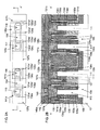
- FIG. 1 is a sectional view illustrating a semiconductor device according to an embodiment of the present invention.
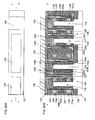
- FIG. 2A is a plan view illustrating a semiconductor device according to an embodiment of the present invention and FIG. 2B is a sectional view taken along line X-X′ in FIG. 2A .
- FIG. 3A is a plan view illustrating a method for producing a semiconductor device according to an embodiment of the present invention and FIG. 3B is a sectional view taken along line X-X′ in FIG. 3A .
- FIG. 4A is a plan view illustrating a method for producing a semiconductor device according to an embodiment of the present invention and FIG. 4B is a sectional view taken along line X-X′ in FIG. 4A .
- FIG. 5A is a plan view illustrating a method for producing a semiconductor device according to an embodiment of the present invention and FIG. 5B is a sectional view taken along line X-X′ in FIG. 5A .
- FIG. 6A is a plan view illustrating a method for producing a semiconductor device according to an embodiment of the present invention and FIG. 6B is a sectional view taken along line X-X′ in FIG. 6A .
- FIG. 7A is a plan view illustrating a method for producing a semiconductor device according to an embodiment of the present invention and FIG. 7B is a sectional view taken along line X-X′ in FIG. 7A .
- FIG. 8A is a plan view illustrating a method for producing a semiconductor device according to an embodiment of the present invention and FIG. 8B is a sectional view taken along line X-X′ in FIG. 8A .
- FIG. 9A is a plan view illustrating a method for producing a semiconductor device according to an embodiment of the present invention and FIG. 9B is a sectional view taken along line X-X′ in FIG. 9A .
- FIG. 10A is a plan view illustrating a method for producing a semiconductor device according to an embodiment of the present invention and FIG. 10B is a sectional view taken along line X-X′ in FIG. 10A .
- FIG. 11A is a plan view illustrating a method for producing a semiconductor device according to an embodiment of the present invention and FIG. 11B is a sectional view taken along line X-X′ in FIG. 11A .
- FIG. 12A is a plan view illustrating a method for producing a semiconductor device according to an embodiment of the present invention and FIG. 12B is a sectional view taken along line X-X′ in FIG. 12A .
- FIG. 13A is a plan view illustrating a method for producing a semiconductor device according to an embodiment of the present invention and FIG. 13B is a sectional view taken along line X-X′ in FIG. 13A .
- FIG. 14A is a plan view illustrating a method for producing a semiconductor device according to an embodiment of the present invention and FIG. 14B is a sectional view taken along line X-X′ in FIG. 14A .
- FIG. 15A is a plan view illustrating a method for producing a semiconductor device according to an embodiment of the present invention and FIG. 15B is a sectional view taken along line X-X′ in FIG. 15A .
- FIG. 16A is a plan view illustrating a method for producing a semiconductor device according to an embodiment of the present invention and FIG. 16B is a sectional view taken along line X-X′ in FIG. 16A .
- FIG. 17A is a plan view illustrating a method for producing a semiconductor device according to an embodiment of the present invention and FIG. 17B is a sectional view taken along line X-X′ in FIG. 17A .
- FIG. 18A is a plan view illustrating a method for producing a semiconductor device according to an embodiment of the present invention and FIG. 18B is a sectional view taken along line X-X′ in FIG. 18A .
- FIG. 19A is a plan view illustrating a method for producing a semiconductor device according to an embodiment of the present invention and FIG. 19B is a sectional view taken along line X-X′ in FIG. 19A .
- FIG. 20A is a plan view illustrating a method for producing a semiconductor device according to an embodiment of the present invention and FIG. 20B is a sectional view taken along line X-X′ in FIG. 20A .
- FIG. 21A is a plan view illustrating a method for producing a semiconductor device according to an embodiment of the present invention and FIG. 21B is a sectional view taken along line X-X′ in FIG. 21A .
- FIG. 22A is a plan view illustrating a method for producing a semiconductor device according to an embodiment of the present invention and FIG. 22B is a sectional view taken along line X-X′ in FIG. 22A .
- FIG. 23A is a plan view illustrating a method for producing a semiconductor device according to an embodiment of the present invention and FIG. 23B is a sectional view taken along line X-X′ in FIG. 23A .
- FIG. 24A is a plan view illustrating a method for producing a semiconductor device according to an embodiment of the present invention and FIG. 24B is a sectional view taken along line X-X′ in FIG. 24A .
- FIG. 25A is a plan view illustrating a method for producing a semiconductor device according to an embodiment of the present invention and FIG. 25B is a sectional view taken along line X-X′ in FIG. 25A .
- FIG. 26A is a plan view illustrating a method for producing a semiconductor device according to an embodiment of the present invention and FIG. 26B is a sectional view taken along line X-X′ in FIG. 26A .
- FIG. 27A is a plan view illustrating a method for producing a semiconductor device according to an embodiment of the present invention and FIG. 27B is a sectional view taken along line X-X′ in FIG. 27A .
- FIG. 28A is a plan view illustrating a method for producing a semiconductor device according to an embodiment of the present invention and FIG. 28B is a sectional view taken along line X-X′ in FIG. 28A .
- FIG. 29A is a plan view illustrating a method for producing a semiconductor device according to an embodiment of the present invention and FIG. 29B is a sectional view taken along line X-X′ in FIG. 29A .
- FIG. 30A is a plan view illustrating a method for producing a semiconductor device according to an embodiment of the present invention and FIG. 30B is a sectional view taken along line X-X′ in FIG. 30A .
- FIG. 31A is a plan view illustrating a method for producing a semiconductor device according to an embodiment of the present invention and FIG. 31B is a sectional view taken along line X-X′ in FIG. 31A .
- FIG. 32A is a plan view illustrating a method for producing a semiconductor device according to an embodiment of the present invention and FIG. 32B is a sectional view taken along line X-X′ in FIG. 32A .
- FIG. 33A is a plan view illustrating a method for producing a semiconductor device according to an embodiment of the present invention and FIG. 33B is a sectional view taken along line X-X′ in FIG. 33A .
- FIG. 34A is a plan view illustrating a method for producing a semiconductor device according to an embodiment of the present invention and FIG. 34B is a sectional view taken along line X-X′ in FIG. 34A .
- FIG. 35A is a plan view illustrating a method for producing a semiconductor device according to an embodiment of the present invention and FIG. 35B is a sectional view taken along line X-X′ in FIG. 35A .
- FIG. 36A is a plan view illustrating a method for producing a semiconductor device according to an embodiment of the present invention and FIG. 36B is a sectional view taken along line X-X′ in FIG. 36A .
- FIG. 37A is a plan view illustrating a method for producing a semiconductor device according to an embodiment of the present invention and FIG. 37B is a sectional view taken along line X-X′ in FIG. 37A .
- FIG. 38A is a plan view illustrating a method for producing a semiconductor device according to an embodiment of the present invention and FIG. 38B is a sectional view taken along line X-X′ in FIG. 38A .
- FIG. 39A is a plan view illustrating a method for producing a semiconductor device according to an embodiment of the present invention and FIG. 39B is a sectional view taken along line X-X′ in FIG. 39A .
- FIG. 40A is a plan view illustrating a method for producing a semiconductor device according to an embodiment of the present invention and FIG. 40B is a sectional view taken along line X-X′ in FIG. 40A .
- FIG. 41A is a plan view illustrating a method for producing a semiconductor device according to an embodiment of the present invention and FIG. 41B is a sectional view taken along line X-X′ in FIG. 41A .
- FIG. 42A is a plan view illustrating a method for producing a semiconductor device according to an embodiment of the present invention and FIG. 42B is a sectional view taken along line X-X′ in FIG. 42A .
- FIG. 43A is a plan view illustrating a method for producing a semiconductor device according to an embodiment of the present invention and FIG. 43B is a sectional view taken along line X-X′ in FIG. 43A .
- FIG. 44A is a plan view illustrating a method for producing a semiconductor device according to an embodiment of the present invention and FIG. 44B is a sectional view taken along line X-X′ in FIG. 44A .
- FIG. 45A is a plan view illustrating a method for producing a semiconductor device according to an embodiment of the present invention and FIG. 45B is a sectional view taken along line X-X′ in FIG. 45A .
- FIG. 1 illustrates a structure of a semiconductor device according to an embodiment of the present invention.
- a semiconductor device illustrated in FIG. 1 includes a first pillar-shaped semiconductor layer 201 , a first selection gate insulating film 221 surrounding the first pillar-shaped semiconductor layer 201 , a first selection gate 237 surrounding the first selection gate insulating film 221 , a first gate insulating film 250 surrounding an upper portion of the first pillar-shaped semiconductor layer 201 , a first contact electrode 258 surrounding the first gate insulating film 250 , and a first bit line 245 connected to an upper portion of the first pillar-shaped semiconductor layer 201 and an upper portion of the first contact electrode 258 .
- a third selection gate insulating film 213 surrounding the first pillar-shaped semiconductor layer 201 and a third selection gate 229 surrounding the third selection gate insulating film 213 are formed below the first selection gate 237 .
- the gate formed below the first selection gate 237 may be a control gate. Furthermore, a layer including a charge storage layer may be used instead of the third selection gate insulating film 213 .
- the semiconductor device illustrated in FIG. 1 further includes a second pillar-shaped semiconductor layer 202 ; a layer 214 including a first charge storage layer and surrounding the second pillar-shaped semiconductor layer 202 ; a first control gate 230 surrounding the layer 214 including the first charge storage layer; a layer 222 including a second charge storage layer, surrounding the second pillar-shaped semiconductor layer 202 , and formed above the first control gate 230 ; a second control gate 238 surrounding the layer 222 including the second charge storage layer; a second gate insulating film 251 surrounding an upper portion of the second pillar-shaped semiconductor layer 202 ; a second contact electrode 259 surrounding the second gate insulating film 251 ; and a first lower internal line 209 that connects a lower portion of the first pillar-shaped semiconductor layer 201 and a lower portion of the second pillar-shaped semiconductor layer 202 .
- An upper portion of the second pillar-shaped semiconductor layer 202 and an upper portion of the second contact electrode 259 are connected to each other.
- the layer including a charge storage layer preferably includes a nitride film as the charge storage layer, and may have a laminated structure of oxide film/nitride film/oxide film.
- a polysilicon may be used for the charge storage layer.
- the layer including a charge storage layer may have a laminated structure of oxide film/polysilicon/oxide film.
- the semiconductor device illustrated in FIG. 1 further includes a third pillar-shaped semiconductor layer 207 ; a layer 219 including a third charge storage layer and surrounding the third pillar-shaped semiconductor layer 207 ; a third control gate 235 surrounding the layer 219 including the third charge storage layer; a layer 227 including a fourth charge storage layer, surrounding the third pillar-shaped semiconductor layer 207 , and formed above the third control gate 235 ; a fourth control gate 243 surrounding the layer 227 including the fourth charge storage layer; a third gate insulating film 256 surrounding an upper portion of the third pillar-shaped semiconductor layer 207 ; and a third contact electrode 264 surrounding the third gate insulating film 256 .
- An upper portion of the third pillar-shaped semiconductor layer 207 and an upper portion of the third contact electrode 264 are connected to each other.
- the semiconductor device illustrated in FIG. 1 further includes a fourth pillar-shaped semiconductor layer 208 , a second selection gate insulating film 228 surrounding the fourth pillar-shaped semiconductor layer 208 , a second selection gate 244 surrounding the second selection gate insulating film 228 , a fourth gate insulating film 257 surrounding an upper portion of the fourth pillar-shaped semiconductor layer 208 , a fourth contact electrode 265 surrounding the fourth gate insulating film 257 , a first source line 249 connected to an upper portion of the fourth pillar-shaped semiconductor layer 208 and the fourth contact electrode 265 , and a second lower internal line 212 that connects a lower portion of the third pillar-shaped semiconductor layer 207 and a lower portion of the fourth pillar-shaped semiconductor layer 208 .
- a fourth selection gate insulating film 220 surrounding the fourth pillar-shaped semiconductor layer 208 and a fourth selection gate 236 surrounding the fourth selection gate insulating film 220 are formed below the second selection gate 244 .
- the gate formed below the second selection gate 244 may be a control gate. Furthermore, a layer including a charge storage layer may be used instead of the fourth selection gate insulating film 220 .
- the second control gate 238 may be one of a plurality of second control gates and the fourth control gate 243 may be one of a plurality of fourth control gates, the second control gates and the fourth control gates being arranged in a direction perpendicular to a substrate.
- the work function of a metal for the first contact electrode 258 , the second contact electrode 259 , the third contact electrode 264 , and the fourth contact electrode 265 is preferably 4.0 eV to 4.2 eV.
- the work function of a metal for the first contact electrode, the second contact electrode, the third contact electrode, and the fourth contact electrode is preferably 5.0 eV to 5.2 eV.
- the semiconductor device illustrated in FIG. 1 further includes a fifth pillar-shaped semiconductor layer 203 ; a layer 215 including a fifth charge storage layer and surrounding the fifth pillar-shaped semiconductor layer 203 ; a fifth control gate 231 surrounding the layer 215 including the fifth charge storage layer; a layer 223 including a sixth charge storage layer, surrounding the fifth pillar-shaped semiconductor layer 203 , and formed above the fifth control gate 231 ; a sixth control gate 239 surrounding the layer 223 including the sixth charge storage layer; a fifth gate insulating film 252 surrounding an upper portion of the fifth pillar-shaped semiconductor layer 203 ; and a fifth contact electrode 260 surrounding the fifth gate insulating film 252 .
- An upper portion of the fifth pillar-shaped semiconductor layer 203 and an upper portion of the fifth contact electrode 260 are connected to each other.
- the semiconductor device illustrated in FIG. 1 further includes a sixth pillar-shaped semiconductor layer 204 ; a layer 216 including a seventh charge storage layer and surrounding the sixth pillar-shaped semiconductor layer 204 ; a seventh control gate 232 surrounding the layer 216 including the seventh charge storage layer; a layer 224 including an eighth charge storage layer, surrounding the sixth pillar-shaped semiconductor layer 204 , and formed above the seventh control gate 232 ; an eighth control gate 240 surrounding the layer 224 including the eighth charge storage layer; a sixth gate insulating film 253 surrounding an upper portion of the sixth pillar-shaped semiconductor layer 204 ; a sixth contact electrode 261 surrounding the sixth gate insulating film 253 ; a third lower internal line 210 that connects a lower portion of the fifth pillar-shaped semiconductor layer 203 and a lower portion of the sixth pillar-shaped semiconductor layer 204 ; and a first upper internal line 246 that connects the upper portion of the second pillar-shaped upper internal line semiconductor layer 202 , the upper portion of the second contact electrode 259
- the semiconductor device also includes a third upper internal line 247 that connects the upper portion of the sixth pillar-shaped semiconductor layer 204 , the upper portion of the sixth contact electrode 261 , and an upper portion of a pillar-shaped semiconductor layer adjacent to the sixth pillar-shaped semiconductor layer 204 .
- the sixth control gate 239 may be one of a plurality of sixth control gates and the eighth control gate 240 may be one of a plurality of eighth control gates, the sixth control gates and the eighth control gates being arranged in a direction perpendicular to a substrate.
- the work function of a metal for the fifth contact electrode and the sixth contact electrode is preferably 4.0 eV to 4.2 eV.
- the work function of a metal for the fifth contact electrode and the sixth contact electrode is preferably 5.0 eV to 5.2 eV.
- the semiconductor device illustrated in FIG. 1 further includes a seventh pillar-shaped semiconductor layer 205 ; a layer 217 including a ninth charge storage layer and surrounding the seventh pillar-shaped semiconductor layer 205 ; a ninth control gate 233 surrounding the layer 217 including the ninth charge storage layer; a layer 225 including a tenth charge storage layer, surrounding the seventh pillar-shaped semiconductor layer 205 , and formed above the ninth control gate 233 ; a tenth control gate 241 surrounding the layer 225 including the tenth charge storage layer; a seventh gate insulating film 254 surrounding an upper portion of the seventh pillar-shaped semiconductor layer 205 , and a seventh contact electrode 262 surrounding the seventh gate insulating film 254 .
- An upper portion of the seventh pillar-shaped semiconductor layer 205 and an upper portion of the seventh contact electrode 262 are connected to each other.
- the semiconductor device illustrated in FIG. 1 further includes an eighth pillar-shaped semiconductor layer 206 ; a layer 218 including an eleventh charge storage layer and surrounding the eighth pillar-shaped semiconductor layer 206 ; an eleventh control gate 234 surrounding the layer 218 including the eleventh charge storage layer; a layer 226 including a twelfth charge storage layer, surrounding the eighth pillar-shaped semiconductor layer 206 , and formed above the eleventh control gate 234 ; a twelfth control gate 242 surrounding the layer 226 including the twelfth charge storage layer; an eighth gate insulating film 255 surrounding an upper portion of the eighth pillar-shaped semiconductor layer 206 ; an eighth contact electrode 263 surrounding the eighth gate insulating film 255 ; a fourth lower internal line 211 that connects a lower portion of the seventh pillar-shaped semiconductor layer 205 and a lower portion of the eighth pillar-shaped semiconductor layer 206 ; and a second upper internal line 248 that connects the upper portion of the third pillar-shaped semiconductor layer 207 , the
- the tenth control gate 241 may be one of a plurality of tenth control gates and the twelfth control gate 242 may be one of a plurality of twelfth control gates, the tenth control gates and the twelfth control gates being arranged in a direction perpendicular to a substrate.
- the work function of a metal for the seventh contact electrode and the eighth contact electrode is preferably 4.0 eV to 4.2 eV.
- the work function of a metal for the seventh contact electrode and the eighth contact electrode is preferably 5.0 eV to 5.2 eV.
- the pillar-shaped semiconductor layer around which a selection gate is formed is the first pillar-shaped semiconductor layer 201 and the fourth pillar-shaped semiconductor layer 208 .
- the pillar-shaped semiconductor layer around which only a control gate is formed is the second pillar-shaped semiconductor layer 202 , the third pillar-shaped semiconductor layer 207 , the fifth pillar-shaped semiconductor layer 203 , the sixth pillar-shaped semiconductor layer 204 , the seventh pillar-shaped semiconductor layer 205 , and the eighth pillar-shaped semiconductor layer 206 .
- the pillar-shaped semiconductor layers 202 , 203 , 204 , 205 , 206 , and 207 (number: m) around which only a control gate is formed are arranged in a line, and the pillar-shaped semiconductor layers 201 and 208 around which a selection gate is formed are disposed at the ends of the line.
- These pillar-shaped semiconductor layers are connected to each other using the lower internal lines 209 , 210 , 211 , and 212 , each of which connects the lower portions of the adjacent pillar-shaped semiconductor layers, and the upper-portion internal lines 246 , 247 , and 248 , each of which connects the upper portions of the adjacent pillar-shaped semiconductor layers, so that the memory cells are connected in series. Therefore, the number of selection gates per pillar-shaped semiconductor layer is 2/m.
- the number of selection gates per pillar-shaped semiconductor layer is 2/32.
- the number of selection gates per pillar-shaped semiconductor layer is 2/64.
- the number of gates can be decreased by one or two. This can decrease the number of production steps.
- FIGS. 2A and 2B illustrate a structure of the semiconductor device.
- a silicon layer is used as a semiconductor layer.
- the semiconductor layer may be formed of another material.
- the semiconductor device illustrated in FIGS. 2A and 2B includes a first pillar-shaped silicon layer 115 , a first selection gate insulating film 133 a surrounding the first pillar-shaped silicon layer 115 , a first selection gate 134 a surrounding the first selection gate insulating film 133 a , a first gate insulating film 135 a surrounding an upper portion of the first pillar-shaped silicon layer 115 , a first contact electrode 141 a surrounding the first gate insulating film 135 a , and a first bit line 137 a connected to an upper portion of the first pillar-shaped silicon layer 115 and the first contact electrode 141 a.
- a third selection gate insulating film 131 a surrounding the first pillar-shaped silicon layer 115 and a third selection gate 132 a surrounding the third selection gate insulating film 131 a are formed below the first selection gate 134 a.
- the gate formed below the first selection gate 134 a may be a control gate. Furthermore, a layer including a charge storage layer may be used instead of the third selection gate insulating film 131 a.
- the semiconductor device illustrated in FIGS. 2A and 2B further includes a second pillar-shaped silicon layer 116 ; a layer 131 b including a first charge storage layer and surrounding the second pillar-shaped silicon layer 116 ; a first control gate 132 b surrounding the layer 131 b including the first charge storage layer; a layer 133 b including a second charge storage layer, surrounding the second pillar-shaped silicon layer 116 , and formed above the first control gate 132 b ; a second control gate 134 b surrounding the layer 133 b including the second charge storage layer; a second gate insulating film 135 b surrounding an upper portion of the second pillar-shaped silicon layer 116 ; a second contact electrode 141 b surrounding the second gate insulating film 135 b ; and a first diffusion layer 127 serving as a first lower internal line that connects a lower portion of the first pillar-shaped silicon layer 115 and a lower portion of the second pillar-shaped silicon layer 116 .
- the semiconductor device illustrated in FIGS. 2A and 2B further includes a first fin-shaped silicon layer 104 formed below the first pillar-shaped silicon layer 115 and the second pillar-shaped silicon layer 116 .
- the first lower internal line is formed in the first fin-shaped silicon layer 104 as the first diffusion layer 127 .
- the semiconductor device illustrated in FIGS. 2A and 2B further includes a third pillar-shaped silicon layer 117 ; a layer 131 c including a third charge storage layer and surrounding the third pillar-shaped silicon layer 117 ; a third control gate 132 c surrounding the layer 131 c including the third charge storage layer; a layer 133 c including a fourth charge storage layer, surrounding the third pillar-shaped silicon layer 117 , and formed above the third control gate 132 c ; a fourth control gate 134 c surrounding the layer 133 c including the fourth charge storage layer; a third gate insulating film 135 c surrounding an upper portion of the third pillar-shaped silicon layer 117 ; and a third contact electrode 141 c surrounding the third gate insulating film 135 c .
- An upper portion of the third pillar-shaped silicon layer 117 and an upper portion of the third contact electrode 141 c are connected to each other.
- the semiconductor device illustrated in FIGS. 2A and 2B further includes a fourth pillar-shaped silicon layer 118 , a second selection gate insulating film 133 d surrounding the fourth pillar-shaped silicon layer 118 , a second selection gate 134 d surrounding the second selection gate insulating film 133 d , a fourth gate insulating film 135 d surrounding an upper portion of the fourth pillar-shaped silicon layer 118 , a fourth contact electrode 136 d surrounding the fourth gate insulating film 135 d , a first source line 137 c connected to an upper portion of the fourth pillar-shaped silicon layer 118 and an upper portion of the fourth contact electrode 136 d , and a second diffusion layer 128 serving as a second lower internal line that connects a lower portion of the third pillar-shaped silicon layer 117 and a lower portion of the fourth pillar-shaped silicon layer 118 .
- a fourth selection gate insulating film 131 d surrounding the fourth pillar-shaped silicon layer 118 and a fourth selection gate 132 d surrounding the fourth selection gate insulating film 131 d are formed below the second selection gate 134 d.
- the gate formed below the second selection gate 134 d may be a control gate. Furthermore, a layer including a charge storage layer may be used instead of the fourth selection gate insulating film 131 d.
- the semiconductor device illustrated in FIGS. 2A and 2B further includes a second fin-shaped silicon layer 105 formed below the third pillar-shaped silicon layer 117 and the fourth pillar-shaped silicon layer 118 .
- the second lower internal line is formed in the second fin-shaped silicon layer 105 as the second diffusion layer 128 .
- a first element separation film 106 is formed around each of the first fin-shaped silicon layer 104 and the second fin-shaped silicon layer 105 .
- memory strings can be formed.
- the semiconductor device illustrated in FIGS. 2A and 2B further includes an upper internal line 137 b that connects the upper portion of the second pillar-shaped silicon layer 116 , the upper portion of the second contact electrode 141 b , the upper portion of the third pillar-shaped silicon layer 117 , and the upper portion of the third contact electrode 141 c.
- the first bit line 137 a is connected to a second bit line 145 a through a contact 146 .
- the pillar-shaped silicon layers are formed on the fin-shaped silicon layers formed on a substrate, the pillar-shaped silicon layers are formed of a single crystal. This avoids a decrease in the mobility of charges due to grain boundaries and consequently avoids a decrease in the readout speed due to grain boundaries.
- control gates can be insulated from the pillar-shaped silicon layers and the fin-shaped silicon layers by the layers including a charge storage layer that are formed around and under the control gates.
- the selection gates can be insulated from the pillar-shaped silicon layers and the selection gates or control gates by the selection gate insulating films formed around and under the selection gates.
- a silicon substrate is used in this embodiment, but a semiconductor substrate other than the silicon substrate may be used.
- first resists 102 and 103 for forming fin-shaped silicon layers are formed on a silicon substrate 101 .
- the silicon substrate 101 is etched to form first and second fin-shaped silicon layers 104 and 105 .
- the fin-shaped silicon layers are formed using the resists as masks, but a hard mask such as an oxide film or a nitride film may be used.
- the first resists 102 and 103 are removed.
- a first element separation film 106 is deposited around the first and second fin-shaped silicon layers 104 and 105 .
- An oxide film formed by using high-density plasma or by low-pressure chemical vapor deposition (CVD) may be used as the first element separation film.
- the first element separation film 106 is etched back to expose upper portions of the first and second fin-shaped silicon layers 104 and 105 .
- second insulating films 107 and 108 are formed around the first and second fin-shaped silicon layers 104 and 105 , respectively.
- the second insulating films 107 and 108 are preferably an oxide film.
- a first polysilicon 109 is deposited on the second insulating films 107 and 108 to perform planarization.
- a third insulating film 110 is formed on the first polysilicon 109 .
- the third insulating film 110 is preferably a nitride film.
- second resists 111 , 112 , 113 , and 114 are formed in a direction perpendicular to a direction in which the first and second fin-shaped silicon layers 104 and 105 extend.
- the third insulating film 110 , the first polysilicon 109 , the second insulating films 107 and 108 , and the first and second fin-shaped silicon layers 104 and 105 are etched to form a first pillar-shaped silicon layer 115 , a second pillar-shaped silicon layer 116 , a third pillar-shaped silicon layer 117 , a fourth pillar-shaped silicon layer 118 , and first dummy gates 109 a , 109 b , 109 c , and 109 d formed of the first polysilicon.
- the third insulating film 110 is divided into third insulating films 110 a , 110 b , 110 c , and 110 d .
- the second insulating films 107 and 108 are divided into second insulating films 107 a , 107 b , 108 a , and 108 b . If the second resists 111 , 112 , 113 , and 114 are removed during the etching, the third insulating films 110 a , 110 b , 110 c , and 110 d function as a hard mask. If the second resists are not removed during the etching, the third insulating film is not necessarily used.
- the second resists 111 , 112 , 113 , and 114 are removed.
- fourth insulating films 119 and 120 are formed around the first pillar-shaped silicon layer 115 , the second pillar-shaped silicon layer 116 , the third pillar-shaped silicon layer 117 , the fourth pillar-shaped silicon layer 118 , and the first dummy gates 109 a , 109 b , 109 c , and 109 d.
- a second polysilicon 126 is deposited around the fourth insulating films 119 and 120 .
- the second polysilicon 126 is etched so as to remain on sidewalls of the first dummy gates 109 a , 109 b , 109 c , and 109 d , the first pillar-shaped silicon layer 115 , the second pillar-shaped silicon layer 116 , the third pillar-shaped silicon layer 117 , and the fourth pillar-shaped silicon layer 118 .
- second dummy gates 126 a , 126 b , 126 c , and 126 d are formed.
- the fourth insulating films 119 and 120 may be divided into fourth insulating films 119 a , 119 b , 120 a , and 120 b .
- An impurity is introduced to form a first diffusion layer 127 and a second diffusion layer 128 in upper portions of the first and second fin-shaped semiconductor layers 104 and 105 , respectively.
- the diffusion layer is an n-type diffusion layer, arsenic or phosphorus is preferably introduced.
- the diffusion layer is a p-type diffusion layer, boron is preferably introduced.
- the diffusion layers may be formed after a sidewall formed of a fifth insulating film described below has been formed.
- a fifth insulating film 129 is formed around the second dummy gates 126 a , 126 b , 126 c , and 126 d .
- the fifth insulating film 129 is preferably a nitride film. Subsequently, the fifth insulating film 129 may be etched so as to be left as sidewalls formed of the fifth insulating film, and metal-semiconductor compound layers may be formed on the first diffusion layer 127 and the second diffusion layer 128 .
- an interlayer insulating film 130 is deposited.
- a contact stopper film may be used.
- chemical mechanical polishing is performed to expose upper portions of the first dummy gates 109 a , 109 b , 109 c , and 109 d and the second dummy gates 126 a , 126 b , 126 c , and 127 d.
- the first dummy gates 109 a , 109 b , 109 c , and 109 d and the second dummy gates 126 a , 126 b , 126 c , and 127 d are removed.
- the second insulating films 107 a , 107 b , 108 a , and 108 b and the fourth insulating films 119 a , 119 b , 120 a , and 120 b are removed.
- a layer 131 including a charge storage layer is formed around the first pillar-shaped silicon layer 115 , the second pillar-shaped silicon layer 116 , the third pillar-shaped silicon layer 117 , and the fourth pillar-shaped silicon layer 118 and on the inner surface of the fifth insulating film 129 .
- the layer 131 including a charge storage layer preferably includes a nitride film.
- the layer 131 may have a laminated structure of oxide film/nitride film/oxide film.
- an insulating film including a nitride film is used as the layer including a charge storage layer.
- Such an insulating film can also be used as a selection gate insulating film.
- a gate conductive film 132 is deposited.
- the gate conductive film 132 is preferably made of a metal.
- the gate conductive film 132 is etched back to form a third selection gate 132 a around the first pillar-shaped silicon layer 115 , a first control gate 132 b around the second pillar-shaped silicon layer 116 , a third control gate 132 c around the third pillar-shaped silicon layer 117 , and a fourth selection gate 132 d around the fourth pillar-shaped silicon layer 118 .
- the exposed layer 131 including a charge storage layer is removed.
- the layer 131 including a charge storage layer is divided into a third selection gate insulating film 131 a , a layer 131 b including a first charge storage layer, a layer 131 c including a third charge storage layer, and a fourth selection gate insulating film 131 d.
- a layer 133 including a charge storage layer is formed around the first pillar-shaped silicon layer 115 , the second pillar-shaped silicon layer 116 , the third pillar-shaped silicon layer 117 , and the fourth pillar-shaped silicon layer 118 and on the inner surface of the fifth insulating film 129 .
- the layer 133 including a charge storage layer preferably includes a nitride film.
- the layer 133 may have a laminated structure of oxide film/nitride film/oxide film.
- an insulating film including a nitride film is used as the layer including a charge storage layer.
- Such an insulating film can also be used as a selection gate insulating film.
- a gate conductive film 134 is deposited.
- the gate conductive film 134 is preferably made of a metal.
- the gate conductive film 134 is etched back to form a first selection gate 134 a around the first pillar-shaped silicon layer 115 , a second control gate 134 b around the second pillar-shaped silicon layer 116 , a fourth control gate 134 c around the third pillar-shaped silicon layer 117 , and a second selection gate 134 d around the fourth pillar-shaped silicon layer 118 .
- the layer 133 including a charge storage layer is removed.
- the layer 133 including a charge storage layer is divided into a first selection gate insulating film 133 a , a layer 133 b including a second charge storage layer, a layer 133 c including a fourth charge storage layer, and a second selection gate insulating film 133 d.
- a gate insulating film 135 to be a first gate insulating film, a second gate insulating film, a third gate insulating film, and a fourth gate insulating film is deposited around upper portions of the first pillar-shaped silicon layer 115 , the second pillar-shaped silicon layer 116 , the third pillar-shaped silicon layer 117 , and the fourth pillar-shaped silicon layer 118 .
- a metal 136 to be a first contact electrode, a second contact electrode, a third contact electrode, and a fourth contact electrode is deposited.
- the metal 136 is etched back to form a first contact electrode line 136 a , a second contact electrode line 136 b , a third contact electrode line 136 c , and a fourth contact electrode line 136 d.
- the exposed gate insulating film 135 is removed.
- the gate insulating film 135 is divided into a first gate insulating film 135 a , a second gate insulating film 135 b , a third gate insulating film 135 c , and a fourth gate insulating film 135 d.
- a metal 137 to be a metal line is deposited.
- third resists 138 , 139 , and 140 for forming a metal line are formed.
- the metal 137 , the first contact electrode line 136 a , the second contact electrode line 136 b , and the third contact electrode line 136 c are etched to form a first bit line 137 a , an upper internal line 137 b , a first source line 137 c , a first contact electrode 141 a , a second contact electrode 141 b , a third contact electrode 141 c , and a fourth contact electrode 136 d.
- the third resists 138 , 139 , and 140 are removed.
- a second interlayer insulating film 142 is deposited.
- a fourth resist 143 for forming a contact is formed.
- the second interlayer insulating film 142 is etched to form a contact hole 144 .
- the fourth resist 143 is removed.
- a metal 145 is deposited.
- the contact hole 144 is filled with the metal, and thus a contact 146 is formed.
- a fifth resist 147 is formed.
- the metal 145 is etched to form a second bit line 145 a.
- the fifth resist 147 is removed.
- a method for producing a semiconductor device in which the p-type (including the p + -type) and the n-type (including the n + -type) are each changed to the opposite conductivity type and a semiconductor device produced by the method are naturally within the technical scope of the present invention.
Landscapes
- Engineering & Computer Science (AREA)
- Microelectronics & Electronic Packaging (AREA)
- Power Engineering (AREA)
- Physics & Mathematics (AREA)
- Condensed Matter Physics & Semiconductors (AREA)
- General Physics & Mathematics (AREA)
- Computer Hardware Design (AREA)
- Ceramic Engineering (AREA)
- Manufacturing & Machinery (AREA)
- Geometry (AREA)
- Semiconductor Memories (AREA)
- Non-Volatile Memory (AREA)
Abstract
A semiconductor device includes a first pillar-shaped semiconductor layer, a first selection gate insulating film, a first selection gate, a first gate insulating film, a first contact electrode, a first bit line connected to an upper portion of the first pillar-shaped semiconductor layer and an upper portion of the first contact electrode, a second pillar-shaped semiconductor layer, a layer including a first charge storage layer, a first control gate, a layer including a second charge storage layer and formed above the first control gate, a second control gate, a second gate insulating film, a second contact electrode having an upper portion connected to an upper portion of the second pillar-shaped semiconductor layer, and a first lower internal line that connects a lower portion of the first pillar-shaped semiconductor layer and a lower portion of the second pillar-shaped semiconductor layer.
Description
This application is a continuation of international patent application PCT/JP2014/055261, filed Mar. 3, 2014, the contents of which are herewith incorporated by reference.
Field of the Invention
The present invention relates to a semiconductor device.
Description of the Related Art
In recent years, semiconductor memory devices in which memory cells are three-dimensionally arranged to increase the degree of integration of memories have been proposed (e.g., refer to Japanese Unexamined Patent Application Publication Nos. 2007-266143 and 2013-4690).
Japanese Unexamined Patent Application Publication No. 2007-266143 discloses that a plurality of memory cells are connected in series in a vertical direction, a drain selection gate is formed above the memory cells, and a source selection gate is formed below the memory cells.
Japanese Unexamined Patent Application Publication No. 2013-4690 discloses that a plurality of memory cells are connected in series in a vertical direction, and a drain selection gate or a source selection gate is formed above the memory cells.
Therefore, according to Japanese Unexamined Patent Application Publication Nos. 2007-266143 and 2013-4690, at least one or two tiers of selection gates are formed in addition to control gates whose number of tiers is equal to that of the memory cells.
When the number of gates is increased, the number of production steps increases.
Furthermore, at least one or two selection gates are formed for each pillar-shaped semiconductor layer. The selection gate itself does not store any information. Moreover, at least one or two circuits for driving a selection gate are required for each pillar-shaped semiconductor layer.
As the width of a silicon pillar decreases, it becomes more difficult to make an impurity be present in the silicon pillar because the density of silicon is 5×10²²/cm3.
In known SGTs, it has been proposed that the channel concentration is set to be a low impurity concentration of 1017 cm−3 or less and the threshold voltage is determined by changing the work function of a gate material (e.g., refer to Japanese Unexamined Patent Application Publication No. 2004-356314).
It has been disclosed that, in planar MOS transistors, the sidewall of an LDD region is formed of a polycrystalline silicon having the same conductivity type as a low-concentration layer, surface carriers of the LDD region are induced by the difference in work function, and thus the impedance of the LDD region can be reduced compared with LDD MOS transistors with an oxide film sidewall (e.g., refer to Japanese Unexamined Patent Application Publication No. 11-297984). It has also been disclosed that the polycrystalline silicon sidewall is electrically insulated from a gate electrode. The drawings show that the polycrystalline silicon sidewall is insulated from a source and a drain by an interlayer insulating film.
It is accordingly an object of the invention to provide a semiconductor device which overcomes the above-mentioned and other disadvantages of the heretofore-known devices and methods of this general type and which provides for a structure of a semiconductor device in which the number of selection gates for each pillar-shaped semiconductor layer is decreased.
A semiconductor device according to an aspect of the present invention includes a first pillar-shaped semiconductor layer; a first selection gate insulating film surrounding the first pillar-shaped semiconductor layer; a first selection gate surrounding the first selection gate insulating film; a first gate insulating film surrounding an upper portion of the first pillar-shaped semiconductor layer; a first contact electrode surrounding the first gate insulating film; a first bit line connected to an upper portion of the first pillar-shaped semiconductor layer and an upper portion of the first contact electrode; a second pillar-shaped semiconductor layer; a layer including a first charge storage layer and surrounding the second pillar-shaped semiconductor layer; a first control gate surrounding the layer including the first charge storage layer; a layer including a second charge storage layer, surrounding the second pillar-shaped semiconductor layer, and formed above the first control gate; a second control gate surrounding the layer including the second charge storage layer; a second gate insulating film surrounding an upper portion of the second pillar-shaped semiconductor layer; a second contact electrode surrounding the second gate insulating film and having an upper portion connected to an upper portion of the second pillar-shaped semiconductor layer; a first lower internal line that connects a lower portion of the first pillar-shaped semiconductor layer and a lower portion of the second pillar-shaped semiconductor layer; a third pillar-shaped semiconductor layer; a layer including a third charge storage layer and surrounding the third pillar-shaped semiconductor layer; a third control gate surrounding the layer including the third charge storage layer; a layer including a fourth charge storage layer, surrounding the third pillar-shaped semiconductor layer, and formed above the third control gate; a fourth control gate surrounding the layer including the fourth charge storage layer; a third gate insulating film surrounding an upper portion of the third pillar-shaped semiconductor layer; a third contact electrode surrounding the third gate insulating film and having an upper portion connected to an upper portion of the third pillar-shaped semiconductor layer; a fourth pillar-shaped semiconductor layer; a second selection gate insulating film surrounding the fourth pillar-shaped semiconductor layer; a second selection gate surrounding the second selection gate insulating film; a fourth gate insulating film surrounding an upper portion of the fourth pillar-shaped semiconductor layer; a fourth contact electrode surrounding the fourth gate insulating film; a first source line connected to an upper portion of the fourth pillar-shaped semiconductor layer and the fourth contact electrode; and a second lower internal line that connects a lower portion of the third pillar-shaped semiconductor layer and a lower portion of the fourth pillar-shaped semiconductor layer.
The second control gate may be one of a plurality of second control gates and the fourth control gate may be one of a plurality of fourth control gates, the second control gates and the fourth control gates being arranged in a direction perpendicular to a substrate.
The semiconductor device may further include a fifth pillar-shaped semiconductor layer; a layer including a fifth charge storage layer and surrounding the fifth pillar-shaped semiconductor layer; a fifth control gate surrounding the layer including the fifth charge storage layer; a layer including a sixth charge storage layer, surrounding the fifth pillar-shaped semiconductor layer, and formed above the fifth control gate; a sixth control gate surrounding the layer including the sixth charge storage layer; a fifth gate insulating film surrounding an upper portion of the fifth pillar-shaped semiconductor layer; a fifth contact electrode surrounding the fifth gate insulating film and having an upper portion connected to an upper portion of the fifth pillar-shaped semiconductor layer; a sixth pillar-shaped semiconductor layer; a layer including a seventh charge storage layer and surrounding the sixth pillar-shaped semiconductor layer; a seventh control gate surrounding the layer including the seventh charge storage layer; a layer including an eighth charge storage layer, surrounding the sixth pillar-shaped semiconductor layer, and formed above the seventh control gate; an eighth control gate surrounding the layer including the eighth charge storage layer; a sixth gate insulating film surrounding an upper portion of the sixth pillar-shaped semiconductor layer; a sixth contact electrode surrounding the sixth gate insulating film and having an upper portion connected to an upper portion of the sixth pillar-shaped semiconductor layer; a third lower internal line that connects a lower portion of the fifth pillar-shaped semiconductor layer and a lower portion of the sixth pillar-shaped semiconductor layer; and a first upper internal line that connects the upper portion of the second pillar-shaped semiconductor layer, the upper portion of the second contact electrode, the upper portion of the fifth pillar-shaped semiconductor layer, and the upper portion of the fifth contact electrode.
The sixth control gate may be one of a plurality of sixth control gates and the eighth control gate may be one of a plurality of eighth control gates, the sixth control gates and the eighth control gates being arranged in a direction perpendicular to a substrate.
The semiconductor device may further include a seventh pillar-shaped semiconductor layer; a layer including a ninth charge storage layer and surrounding the seventh pillar-shaped semiconductor layer; a ninth control gate surrounding the layer including the ninth charge storage layer; a layer including a tenth charge storage layer, surrounding the seventh pillar-shaped semiconductor layer, and formed above the ninth control gate; a tenth control gate surrounding the layer including the tenth charge storage layer; a seventh gate insulating film surrounding an upper portion of the seventh pillar-shaped semiconductor layer; a seventh contact electrode surrounding the seventh gate insulating film and having an upper portion connected to an upper portion of the seventh pillar-shaped semiconductor layer; an eighth pillar-shaped semiconductor layer; a layer including an eleventh charge storage layer and surrounding the eighth pillar-shaped semiconductor layer; an eleventh control gate surrounding the layer including the eleventh charge storage layer; a layer including a twelfth charge storage layer, surrounding the eighth pillar-shaped semiconductor layer, and formed above the eleventh control gate; a twelfth control gate surrounding the layer including the twelfth charge storage layer; an eighth gate insulating film surrounding an upper portion of the eighth pillar-shaped semiconductor layer; an eighth contact electrode surrounding the eighth gate insulating film and having an upper portion connected to an upper portion of the eighth pillar-shaped semiconductor layer; a fourth lower internal line that connects a lower portion of the seventh pillar-shaped semiconductor layer and a lower portion of the eighth pillar-shaped semiconductor layer; and a second upper internal line that connects the upper portion of the third pillar-shaped semiconductor layer, the upper portion of the third contact electrode, the upper portion of the eighth pillar-shaped semiconductor layer, and the upper portion of the eighth contact electrode.
The tenth control gate may be one of a plurality of tenth control gates and the twelfth control gate may be one of a plurality of twelfth control gates, the tenth control gates and the twelfth control gates being arranged in a direction perpendicular to a substrate.
The semiconductor device may further include a first fin-shaped semiconductor layer formed below the first pillar-shaped semiconductor layer and the second pillar-shaped semiconductor layer; and a second fin-shaped semiconductor layer formed below the third pillar-shaped semiconductor layer and the fourth pillar-shaped semiconductor layer, wherein the first lower internal line is formed in the first fin-shaped semiconductor layer, and the second lower internal line is formed in the second fin-shaped semiconductor layer.
The semiconductor device may further include a third fin-shaped semiconductor layer formed below the fifth pillar-shaped semiconductor layer and the sixth pillar-shaped semiconductor layer, wherein the third lower internal line is formed in the third fin-shaped semiconductor layer.
The semiconductor device may further include a fourth fin-shaped semiconductor layer formed below the seventh pillar-shaped semiconductor layer and the eighth pillar-shaped semiconductor layer, wherein the fourth lower internal line is formed in the fourth fin-shaped semiconductor layer.
A first element separation film may be formed around the first fin-shaped semiconductor layer and the second fin-shaped semiconductor layer.
A third selection gate may be formed below the first selection gate.
A fourth selection gate may be formed below the second selection gate.
A thirteenth control gate may be formed below the first selection gate.
A fourteenth control gate may be formed below the second selection gate.
The first lower internal line may be a first diffusion layer, and the second lower internal line may be a second diffusion layer.
The third lower internal line may be a third diffusion layer.
The fourth lower internal line may be a fourth diffusion layer.
A metal for the first contact electrode, the second contact electrode, the third contact electrode, and the fourth contact electrode may have a work function of 4.0 eV to 4.2 eV.
A metal for the first contact electrode, the second contact electrode, the third contact electrode, and the fourth contact electrode may have a work function of 5.0 eV to 5.2 eV.
A metal for the fifth contact electrode and the sixth contact electrode may have a work function of 4.0 eV to 4.2 eV.
A metal for the fifth contact electrode and the sixth contact electrode may have a work function of 5.0 eV to 5.2 eV.
A metal for the seventh contact electrode and the eighth contact electrode may have a work function of 4.0 eV to 4.2 eV.
A metal for the seventh contact electrode and the eighth contact electrode may have a work function of 5.0 eV to 5.2 eV.
The layer including the first charge storage layer may include a nitride film as a charge storage layer.
The present invention can provide a structure of a semiconductor device in which the number of selection gates per pillar-shaped semiconductor layer is decreased.
Pillar-shaped semiconductor layers around which a selection gate is formed and pillar-shaped semiconductor layers around which only a control gate is formed are used. The pillar-shaped semiconductor layers (number: m) around which only a control gate is formed are arranged in a line, and the pillar-shaped semiconductor layers around which a selection gate is formed are disposed at the ends of the line. These pillar-shaped semiconductor layers are connected to each other using lower internal lines, each of which connects lower portions of the adjacent pillar-shaped semiconductor layers, and upper internal lines, each of which connects upper portions of the adjacent pillar-shaped semiconductor layers, so that memory cells are connected in series. Therefore, the number of selection gates per pillar-shaped semiconductor layer is 2/m.
When m is 32, the number of selection gates per pillar-shaped semiconductor layer is 2/32. When m is 64, the number of selection gates per pillar-shaped semiconductor layer is 2/64. Thus, the number of circuits for driving a selection gate can be decreased.
Furthermore, since the pillar-shaped semiconductor layers around which only a control gate is formed are used, the number of gates can be decreased by one or two. This can decrease the number of production steps.
If a metal gate-last process is used for an SGT, an upper portion of a pillar-shaped semiconductor layer is covered with a polysilicon gate. Therefore, it is difficult to form a diffusion layer in the upper portion of the pillar-shaped semiconductor layer. This requires formation of a diffusion layer in the upper portion of the pillar-shaped semiconductor layer before formation of a polysilicon gate. In contrast, according to the present invention, the upper portion of a pillar-shaped semiconductor layer can be made to function as an n-type semiconductor layer or a p-type semiconductor layer by the difference in work function between metal and semiconductor without forming a diffusion layer in the upper portion of the pillar-shaped semiconductor layer. Accordingly, a step of forming a diffusion layer in an upper portion of a pillar-shaped semiconductor layer can be omitted.
Other features which are considered as characteristic for the invention are set forth in the appended claims.
Although the invention is illustrated and described herein as embodied in a semiconductor device, it is nevertheless not intended to be limited to the details shown, since various modifications and structural changes may be made therein without departing from the spirit of the invention and within the scope and range of equivalents of the claims.
The construction and method of operation of the invention, however, together with additional objects and advantages thereof will be best understood from the following description of specific embodiments when read in connection with the accompanying drawings.
A semiconductor device illustrated in FIG. 1 includes a first pillar-shaped semiconductor layer 201, a first selection gate insulating film 221 surrounding the first pillar-shaped semiconductor layer 201, a first selection gate 237 surrounding the first selection gate insulating film 221, a first gate insulating film 250 surrounding an upper portion of the first pillar-shaped semiconductor layer 201, a first contact electrode 258 surrounding the first gate insulating film 250, and a first bit line 245 connected to an upper portion of the first pillar-shaped semiconductor layer 201 and an upper portion of the first contact electrode 258.
A third selection gate insulating film 213 surrounding the first pillar-shaped semiconductor layer 201 and a third selection gate 229 surrounding the third selection gate insulating film 213 are formed below the first selection gate 237.
The gate formed below the first selection gate 237 may be a control gate. Furthermore, a layer including a charge storage layer may be used instead of the third selection gate insulating film 213.
The semiconductor device illustrated in FIG. 1 further includes a second pillar-shaped semiconductor layer 202; a layer 214 including a first charge storage layer and surrounding the second pillar-shaped semiconductor layer 202; a first control gate 230 surrounding the layer 214 including the first charge storage layer; a layer 222 including a second charge storage layer, surrounding the second pillar-shaped semiconductor layer 202, and formed above the first control gate 230; a second control gate 238 surrounding the layer 222 including the second charge storage layer; a second gate insulating film 251 surrounding an upper portion of the second pillar-shaped semiconductor layer 202; a second contact electrode 259 surrounding the second gate insulating film 251; and a first lower internal line 209 that connects a lower portion of the first pillar-shaped semiconductor layer 201 and a lower portion of the second pillar-shaped semiconductor layer 202. An upper portion of the second pillar-shaped semiconductor layer 202 and an upper portion of the second contact electrode 259 are connected to each other.
The layer including a charge storage layer preferably includes a nitride film as the charge storage layer, and may have a laminated structure of oxide film/nitride film/oxide film. A polysilicon may be used for the charge storage layer. The layer including a charge storage layer may have a laminated structure of oxide film/polysilicon/oxide film.
The semiconductor device illustrated in FIG. 1 further includes a third pillar-shaped semiconductor layer 207; a layer 219 including a third charge storage layer and surrounding the third pillar-shaped semiconductor layer 207; a third control gate 235 surrounding the layer 219 including the third charge storage layer; a layer 227 including a fourth charge storage layer, surrounding the third pillar-shaped semiconductor layer 207, and formed above the third control gate 235; a fourth control gate 243 surrounding the layer 227 including the fourth charge storage layer; a third gate insulating film 256 surrounding an upper portion of the third pillar-shaped semiconductor layer 207; and a third contact electrode 264 surrounding the third gate insulating film 256. An upper portion of the third pillar-shaped semiconductor layer 207 and an upper portion of the third contact electrode 264 are connected to each other.
The semiconductor device illustrated in FIG. 1 further includes a fourth pillar-shaped semiconductor layer 208, a second selection gate insulating film 228 surrounding the fourth pillar-shaped semiconductor layer 208, a second selection gate 244 surrounding the second selection gate insulating film 228, a fourth gate insulating film 257 surrounding an upper portion of the fourth pillar-shaped semiconductor layer 208, a fourth contact electrode 265 surrounding the fourth gate insulating film 257, a first source line 249 connected to an upper portion of the fourth pillar-shaped semiconductor layer 208 and the fourth contact electrode 265, and a second lower internal line 212 that connects a lower portion of the third pillar-shaped semiconductor layer 207 and a lower portion of the fourth pillar-shaped semiconductor layer 208.
A fourth selection gate insulating film 220 surrounding the fourth pillar-shaped semiconductor layer 208 and a fourth selection gate 236 surrounding the fourth selection gate insulating film 220 are formed below the second selection gate 244.
The gate formed below the second selection gate 244 may be a control gate. Furthermore, a layer including a charge storage layer may be used instead of the fourth selection gate insulating film 220.
The second control gate 238 may be one of a plurality of second control gates and the fourth control gate 243 may be one of a plurality of fourth control gates, the second control gates and the fourth control gates being arranged in a direction perpendicular to a substrate.
When the transistor is an n-type transistor, the work function of a metal for the first contact electrode 258, the second contact electrode 259, the third contact electrode 264, and the fourth contact electrode 265 is preferably 4.0 eV to 4.2 eV.
When the transistor is a p-type transistor, the work function of a metal for the first contact electrode, the second contact electrode, the third contact electrode, and the fourth contact electrode is preferably 5.0 eV to 5.2 eV.
The semiconductor device illustrated in FIG. 1 further includes a fifth pillar-shaped semiconductor layer 203; a layer 215 including a fifth charge storage layer and surrounding the fifth pillar-shaped semiconductor layer 203; a fifth control gate 231 surrounding the layer 215 including the fifth charge storage layer; a layer 223 including a sixth charge storage layer, surrounding the fifth pillar-shaped semiconductor layer 203, and formed above the fifth control gate 231; a sixth control gate 239 surrounding the layer 223 including the sixth charge storage layer; a fifth gate insulating film 252 surrounding an upper portion of the fifth pillar-shaped semiconductor layer 203; and a fifth contact electrode 260 surrounding the fifth gate insulating film 252. An upper portion of the fifth pillar-shaped semiconductor layer 203 and an upper portion of the fifth contact electrode 260 are connected to each other.
The semiconductor device illustrated in FIG. 1 further includes a sixth pillar-shaped semiconductor layer 204; a layer 216 including a seventh charge storage layer and surrounding the sixth pillar-shaped semiconductor layer 204; a seventh control gate 232 surrounding the layer 216 including the seventh charge storage layer; a layer 224 including an eighth charge storage layer, surrounding the sixth pillar-shaped semiconductor layer 204, and formed above the seventh control gate 232; an eighth control gate 240 surrounding the layer 224 including the eighth charge storage layer; a sixth gate insulating film 253 surrounding an upper portion of the sixth pillar-shaped semiconductor layer 204; a sixth contact electrode 261 surrounding the sixth gate insulating film 253; a third lower internal line 210 that connects a lower portion of the fifth pillar-shaped semiconductor layer 203 and a lower portion of the sixth pillar-shaped semiconductor layer 204; and a first upper internal line 246 that connects the upper portion of the second pillar-shaped upper internal line semiconductor layer 202, the upper portion of the second contact electrode 259, the upper portion of the fifth pillar-shaped semiconductor layer 203, and the upper portion of the fifth contact electrode 260. An upper portion of the sixth pillar-shaped semiconductor layer 204 and an upper portion of the sixth contact electrode 261 are connected to each other. The semiconductor device also includes a third upper internal line 247 that connects the upper portion of the sixth pillar-shaped semiconductor layer 204, the upper portion of the sixth contact electrode 261, and an upper portion of a pillar-shaped semiconductor layer adjacent to the sixth pillar-shaped semiconductor layer 204.
The sixth control gate 239 may be one of a plurality of sixth control gates and the eighth control gate 240 may be one of a plurality of eighth control gates, the sixth control gates and the eighth control gates being arranged in a direction perpendicular to a substrate.
When the transistor is an n-type transistor, the work function of a metal for the fifth contact electrode and the sixth contact electrode is preferably 4.0 eV to 4.2 eV.
When the transistor is a p-type transistor, the work function of a metal for the fifth contact electrode and the sixth contact electrode is preferably 5.0 eV to 5.2 eV.
The semiconductor device illustrated in FIG. 1 further includes a seventh pillar-shaped semiconductor layer 205; a layer 217 including a ninth charge storage layer and surrounding the seventh pillar-shaped semiconductor layer 205; a ninth control gate 233 surrounding the layer 217 including the ninth charge storage layer; a layer 225 including a tenth charge storage layer, surrounding the seventh pillar-shaped semiconductor layer 205, and formed above the ninth control gate 233; a tenth control gate 241 surrounding the layer 225 including the tenth charge storage layer; a seventh gate insulating film 254 surrounding an upper portion of the seventh pillar-shaped semiconductor layer 205, and a seventh contact electrode 262 surrounding the seventh gate insulating film 254. An upper portion of the seventh pillar-shaped semiconductor layer 205 and an upper portion of the seventh contact electrode 262 are connected to each other.
The semiconductor device illustrated in FIG. 1 further includes an eighth pillar-shaped semiconductor layer 206; a layer 218 including an eleventh charge storage layer and surrounding the eighth pillar-shaped semiconductor layer 206; an eleventh control gate 234 surrounding the layer 218 including the eleventh charge storage layer; a layer 226 including a twelfth charge storage layer, surrounding the eighth pillar-shaped semiconductor layer 206, and formed above the eleventh control gate 234; a twelfth control gate 242 surrounding the layer 226 including the twelfth charge storage layer; an eighth gate insulating film 255 surrounding an upper portion of the eighth pillar-shaped semiconductor layer 206; an eighth contact electrode 263 surrounding the eighth gate insulating film 255; a fourth lower internal line 211 that connects a lower portion of the seventh pillar-shaped semiconductor layer 205 and a lower portion of the eighth pillar-shaped semiconductor layer 206; and a second upper internal line 248 that connects the upper portion of the third pillar-shaped semiconductor layer 207, the upper portion of the third contact electrode 264, the upper portion of the eighth pillar-shaped semiconductor layer 206, and the upper portion of the eighth contact electrode 263. An upper portion of the eighth pillar-shaped semiconductor layer 206 and an upper portion of the eighth contact electrode 263 are connected to each other.
The tenth control gate 241 may be one of a plurality of tenth control gates and the twelfth control gate 242 may be one of a plurality of twelfth control gates, the tenth control gates and the twelfth control gates being arranged in a direction perpendicular to a substrate.
When the transistor is an n-type transistor, the work function of a metal for the seventh contact electrode and the eighth contact electrode is preferably 4.0 eV to 4.2 eV.
When the transistor is a p-type transistor, the work function of a metal for the seventh contact electrode and the eighth contact electrode is preferably 5.0 eV to 5.2 eV.
The pillar-shaped semiconductor layer around which a selection gate is formed is the first pillar-shaped semiconductor layer 201 and the fourth pillar-shaped semiconductor layer 208. The pillar-shaped semiconductor layer around which only a control gate is formed is the second pillar-shaped semiconductor layer 202, the third pillar-shaped semiconductor layer 207, the fifth pillar-shaped semiconductor layer 203, the sixth pillar-shaped semiconductor layer 204, the seventh pillar-shaped semiconductor layer 205, and the eighth pillar-shaped semiconductor layer 206.
The pillar-shaped semiconductor layers 202, 203, 204, 205, 206, and 207 (number: m) around which only a control gate is formed are arranged in a line, and the pillar-shaped semiconductor layers 201 and 208 around which a selection gate is formed are disposed at the ends of the line. These pillar-shaped semiconductor layers are connected to each other using the lower internal lines 209, 210, 211, and 212, each of which connects the lower portions of the adjacent pillar-shaped semiconductor layers, and the upper-portion internal lines 246, 247, and 248, each of which connects the upper portions of the adjacent pillar-shaped semiconductor layers, so that the memory cells are connected in series. Therefore, the number of selection gates per pillar-shaped semiconductor layer is 2/m.
When m is 32, the number of selection gates per pillar-shaped semiconductor layer is 2/32. When m is 64, the number of selection gates per pillar-shaped semiconductor layer is 2/64. Thus, the number of circuits for driving a selection gate can be decreased.
Furthermore, since the pillar-shaped semiconductor layers around which only a control gate is formed are used, the number of gates can be decreased by one or two. This can decrease the number of production steps.
The semiconductor device illustrated in FIGS. 2A and 2B includes a first pillar-shaped silicon layer 115, a first selection gate insulating film 133 a surrounding the first pillar-shaped silicon layer 115, a first selection gate 134 a surrounding the first selection gate insulating film 133 a, a first gate insulating film 135 a surrounding an upper portion of the first pillar-shaped silicon layer 115, a first contact electrode 141 a surrounding the first gate insulating film 135 a, and a first bit line 137 a connected to an upper portion of the first pillar-shaped silicon layer 115 and the first contact electrode 141 a.
A third selection gate insulating film 131 a surrounding the first pillar-shaped silicon layer 115 and a third selection gate 132 a surrounding the third selection gate insulating film 131 a are formed below the first selection gate 134 a.
The gate formed below the first selection gate 134 a may be a control gate. Furthermore, a layer including a charge storage layer may be used instead of the third selection gate insulating film 131 a.
The semiconductor device illustrated in FIGS. 2A and 2B further includes a second pillar-shaped silicon layer 116; a layer 131 b including a first charge storage layer and surrounding the second pillar-shaped silicon layer 116; a first control gate 132 b surrounding the layer 131 b including the first charge storage layer; a layer 133 b including a second charge storage layer, surrounding the second pillar-shaped silicon layer 116, and formed above the first control gate 132 b; a second control gate 134 b surrounding the layer 133 b including the second charge storage layer; a second gate insulating film 135 b surrounding an upper portion of the second pillar-shaped silicon layer 116; a second contact electrode 141 b surrounding the second gate insulating film 135 b; and a first diffusion layer 127 serving as a first lower internal line that connects a lower portion of the first pillar-shaped silicon layer 115 and a lower portion of the second pillar-shaped silicon layer 116. An upper portion of the second pillar-shaped silicon layer 116 and an upper portion of the second contact electrode 141 b are connected to each other.
The semiconductor device illustrated in FIGS. 2A and 2B further includes a first fin-shaped silicon layer 104 formed below the first pillar-shaped silicon layer 115 and the second pillar-shaped silicon layer 116. The first lower internal line is formed in the first fin-shaped silicon layer 104 as the first diffusion layer 127.
The semiconductor device illustrated in FIGS. 2A and 2B further includes a third pillar-shaped silicon layer 117; a layer 131 c including a third charge storage layer and surrounding the third pillar-shaped silicon layer 117; a third control gate 132 c surrounding the layer 131 c including the third charge storage layer; a layer 133 c including a fourth charge storage layer, surrounding the third pillar-shaped silicon layer 117, and formed above the third control gate 132 c; a fourth control gate 134 c surrounding the layer 133 c including the fourth charge storage layer; a third gate insulating film 135 c surrounding an upper portion of the third pillar-shaped silicon layer 117; and a third contact electrode 141 c surrounding the third gate insulating film 135 c. An upper portion of the third pillar-shaped silicon layer 117 and an upper portion of the third contact electrode 141 c are connected to each other.
The semiconductor device illustrated in FIGS. 2A and 2B further includes a fourth pillar-shaped silicon layer 118, a second selection gate insulating film 133 d surrounding the fourth pillar-shaped silicon layer 118, a second selection gate 134 d surrounding the second selection gate insulating film 133 d, a fourth gate insulating film 135 d surrounding an upper portion of the fourth pillar-shaped silicon layer 118, a fourth contact electrode 136 d surrounding the fourth gate insulating film 135 d, a first source line 137 c connected to an upper portion of the fourth pillar-shaped silicon layer 118 and an upper portion of the fourth contact electrode 136 d, and a second diffusion layer 128 serving as a second lower internal line that connects a lower portion of the third pillar-shaped silicon layer 117 and a lower portion of the fourth pillar-shaped silicon layer 118.
A fourth selection gate insulating film 131 d surrounding the fourth pillar-shaped silicon layer 118 and a fourth selection gate 132 d surrounding the fourth selection gate insulating film 131 d are formed below the second selection gate 134 d.
The gate formed below the second selection gate 134 d may be a control gate. Furthermore, a layer including a charge storage layer may be used instead of the fourth selection gate insulating film 131 d.
The semiconductor device illustrated in FIGS. 2A and 2B further includes a second fin-shaped silicon layer 105 formed below the third pillar-shaped silicon layer 117 and the fourth pillar-shaped silicon layer 118. The second lower internal line is formed in the second fin-shaped silicon layer 105 as the second diffusion layer 128.
A first element separation film 106 is formed around each of the first fin-shaped silicon layer 104 and the second fin-shaped silicon layer 105.
Since elements are separated by the first element separation film 106 formed around each of the fin-shaped semiconductor layers, memory strings can be formed.
The semiconductor device illustrated in FIGS. 2A and 2B further includes an upper internal line 137 b that connects the upper portion of the second pillar-shaped silicon layer 116, the upper portion of the second contact electrode 141 b, the upper portion of the third pillar-shaped silicon layer 117, and the upper portion of the third contact electrode 141 c.
The first bit line 137 a is connected to a second bit line 145 a through a contact 146.
Since the pillar-shaped silicon layers are formed on the fin-shaped silicon layers formed on a substrate, the pillar-shaped silicon layers are formed of a single crystal. This avoids a decrease in the mobility of charges due to grain boundaries and consequently avoids a decrease in the readout speed due to grain boundaries.
The control gates can be insulated from the pillar-shaped silicon layers and the fin-shaped silicon layers by the layers including a charge storage layer that are formed around and under the control gates.
The selection gates can be insulated from the pillar-shaped silicon layers and the selection gates or control gates by the selection gate insulating films formed around and under the selection gates.
Hereafter, a production process for forming a structure of a semiconductor device according to an embodiment of the present invention will be described with reference to FIG. 3A to FIG. 45B . A silicon substrate is used in this embodiment, but a semiconductor substrate other than the silicon substrate may be used.
As illustrated in FIGS. 3A and 3B , first resists 102 and 103 for forming fin-shaped silicon layers are formed on a silicon substrate 101.
As illustrated in FIGS. 4A and 4B , the silicon substrate 101 is etched to form first and second fin-shaped silicon layers 104 and 105. In this case, the fin-shaped silicon layers are formed using the resists as masks, but a hard mask such as an oxide film or a nitride film may be used.
As illustrated in FIGS. 5A and 5B , the first resists 102 and 103 are removed.
As illustrated in FIGS. 6A and 6B , a first element separation film 106 is deposited around the first and second fin-shaped silicon layers 104 and 105. An oxide film formed by using high-density plasma or by low-pressure chemical vapor deposition (CVD) may be used as the first element separation film.
As illustrated in FIGS. 7A and 7B , the first element separation film 106 is etched back to expose upper portions of the first and second fin-shaped silicon layers 104 and 105.
As illustrated in FIGS. 8A and 8B , second insulating films 107 and 108 are formed around the first and second fin-shaped silicon layers 104 and 105, respectively. The second insulating films 107 and 108 are preferably an oxide film.
As illustrated in FIGS. 9A and 9B , a first polysilicon 109 is deposited on the second insulating films 107 and 108 to perform planarization.
As illustrated in FIGS. 10A and 10B , a third insulating film 110 is formed on the first polysilicon 109. The third insulating film 110 is preferably a nitride film.
As illustrated in FIGS. 11A and 11B , second resists 111, 112, 113, and 114 are formed in a direction perpendicular to a direction in which the first and second fin-shaped silicon layers 104 and 105 extend.
As illustrated in FIGS. 12A and 12B , the third insulating film 110, the first polysilicon 109, the second insulating films 107 and 108, and the first and second fin-shaped silicon layers 104 and 105 are etched to form a first pillar-shaped silicon layer 115, a second pillar-shaped silicon layer 116, a third pillar-shaped silicon layer 117, a fourth pillar-shaped silicon layer 118, and first dummy gates 109 a, 109 b, 109 c, and 109 d formed of the first polysilicon. As a result, the third insulating film 110 is divided into third insulating films 110 a, 110 b, 110 c, and 110 d. The second insulating films 107 and 108 are divided into second insulating films 107 a, 107 b, 108 a, and 108 b. If the second resists 111, 112, 113, and 114 are removed during the etching, the third insulating films 110 a, 110 b, 110 c, and 110 d function as a hard mask. If the second resists are not removed during the etching, the third insulating film is not necessarily used.
As illustrated in FIGS. 13A and 13B , the second resists 111, 112, 113, and 114 are removed.
As illustrated in FIGS. 14A and 14B , fourth insulating films 119 and 120 are formed around the first pillar-shaped silicon layer 115, the second pillar-shaped silicon layer 116, the third pillar-shaped silicon layer 117, the fourth pillar-shaped silicon layer 118, and the first dummy gates 109 a, 109 b, 109 c, and 109 d.
As illustrated in FIGS. 15A and 15B , a second polysilicon 126 is deposited around the fourth insulating films 119 and 120.
As illustrated in FIGS. 16A and 16B , the second polysilicon 126 is etched so as to remain on sidewalls of the first dummy gates 109 a, 109 b, 109 c, and 109 d, the first pillar-shaped silicon layer 115, the second pillar-shaped silicon layer 116, the third pillar-shaped silicon layer 117, and the fourth pillar-shaped silicon layer 118. Thus, second dummy gates 126 a, 126 b, 126 c, and 126 d are formed. Herein, the fourth insulating films 119 and 120 may be divided into fourth insulating films 119 a, 119 b, 120 a, and 120 b. An impurity is introduced to form a first diffusion layer 127 and a second diffusion layer 128 in upper portions of the first and second fin-shaped semiconductor layers 104 and 105, respectively. When the diffusion layer is an n-type diffusion layer, arsenic or phosphorus is preferably introduced. When the diffusion layer is a p-type diffusion layer, boron is preferably introduced. The diffusion layers may be formed after a sidewall formed of a fifth insulating film described below has been formed.
As illustrated in FIGS. 17A and 17B , a fifth insulating film 129 is formed around the second dummy gates 126 a, 126 b, 126 c, and 126 d. The fifth insulating film 129 is preferably a nitride film. Subsequently, the fifth insulating film 129 may be etched so as to be left as sidewalls formed of the fifth insulating film, and metal-semiconductor compound layers may be formed on the first diffusion layer 127 and the second diffusion layer 128.
As illustrated in FIGS. 18A and 18B , an interlayer insulating film 130 is deposited. A contact stopper film may be used.
As illustrated in FIGS. 19A and 19B , chemical mechanical polishing is performed to expose upper portions of the first dummy gates 109 a, 109 b, 109 c, and 109 d and the second dummy gates 126 a, 126 b, 126 c, and 127 d.
As illustrated in FIGS. 20A and 20B , the first dummy gates 109 a, 109 b, 109 c, and 109 d and the second dummy gates 126 a, 126 b, 126 c, and 127 d are removed.
As illustrated in FIGS. 21A and 21B , the second insulating films 107 a, 107 b, 108 a, and 108 b and the fourth insulating films 119 a, 119 b, 120 a, and 120 b are removed.
As illustrated in FIGS. 22A and 22B , a layer 131 including a charge storage layer is formed around the first pillar-shaped silicon layer 115, the second pillar-shaped silicon layer 116, the third pillar-shaped silicon layer 117, and the fourth pillar-shaped silicon layer 118 and on the inner surface of the fifth insulating film 129. The layer 131 including a charge storage layer preferably includes a nitride film. Alternatively, the layer 131 may have a laminated structure of oxide film/nitride film/oxide film. In this embodiment of the production method, an insulating film including a nitride film is used as the layer including a charge storage layer. Such an insulating film can also be used as a selection gate insulating film.
As illustrated in FIGS. 23A and 23B , a gate conductive film 132 is deposited. The gate conductive film 132 is preferably made of a metal.
As illustrated in FIGS. 24A and 24B , the gate conductive film 132 is etched back to form a third selection gate 132 a around the first pillar-shaped silicon layer 115, a first control gate 132 b around the second pillar-shaped silicon layer 116, a third control gate 132 c around the third pillar-shaped silicon layer 117, and a fourth selection gate 132 d around the fourth pillar-shaped silicon layer 118.
As illustrated in FIGS. 25A and 25B , the exposed layer 131 including a charge storage layer is removed. The layer 131 including a charge storage layer is divided into a third selection gate insulating film 131 a, a layer 131 b including a first charge storage layer, a layer 131 c including a third charge storage layer, and a fourth selection gate insulating film 131 d.
As illustrated in FIGS. 26A and 26B , a layer 133 including a charge storage layer is formed around the first pillar-shaped silicon layer 115, the second pillar-shaped silicon layer 116, the third pillar-shaped silicon layer 117, and the fourth pillar-shaped silicon layer 118 and on the inner surface of the fifth insulating film 129. The layer 133 including a charge storage layer preferably includes a nitride film. Alternatively, the layer 133 may have a laminated structure of oxide film/nitride film/oxide film. In this embodiment of the production method, an insulating film including a nitride film is used as the layer including a charge storage layer. Such an insulating film can also be used as a selection gate insulating film.
As illustrated in FIGS. 27A and 27B , a gate conductive film 134 is deposited. The gate conductive film 134 is preferably made of a metal.
As illustrated in FIGS. 28A and 28B , the gate conductive film 134 is etched back to form a first selection gate 134 a around the first pillar-shaped silicon layer 115, a second control gate 134 b around the second pillar-shaped silicon layer 116, a fourth control gate 134 c around the third pillar-shaped silicon layer 117, and a second selection gate 134 d around the fourth pillar-shaped silicon layer 118.
As illustrated in FIGS. 29A and 29B , the layer 133 including a charge storage layer is removed. The layer 133 including a charge storage layer is divided into a first selection gate insulating film 133 a, a layer 133 b including a second charge storage layer, a layer 133 c including a fourth charge storage layer, and a second selection gate insulating film 133 d.
As illustrated in FIGS. 30A and 30B , a gate insulating film 135 to be a first gate insulating film, a second gate insulating film, a third gate insulating film, and a fourth gate insulating film is deposited around upper portions of the first pillar-shaped silicon layer 115, the second pillar-shaped silicon layer 116, the third pillar-shaped silicon layer 117, and the fourth pillar-shaped silicon layer 118.
As illustrated in FIGS. 31A and 31B , a metal 136 to be a first contact electrode, a second contact electrode, a third contact electrode, and a fourth contact electrode is deposited.
As illustrated in FIGS. 32A and 32B , the metal 136 is etched back to form a first contact electrode line 136 a, a second contact electrode line 136 b, a third contact electrode line 136 c, and a fourth contact electrode line 136 d.
As illustrated in FIGS. 33A and 33B , the exposed gate insulating film 135 is removed. The gate insulating film 135 is divided into a first gate insulating film 135 a, a second gate insulating film 135 b, a third gate insulating film 135 c, and a fourth gate insulating film 135 d.
As illustrated in FIGS. 34A and 34B , a metal 137 to be a metal line is deposited.
As illustrated in FIGS. 35A and 35B , third resists 138, 139, and 140 for forming a metal line are formed.
As illustrated in FIGS. 36A and 36B , the metal 137, the first contact electrode line 136 a, the second contact electrode line 136 b, and the third contact electrode line 136 c are etched to form a first bit line 137 a, an upper internal line 137 b, a first source line 137 c, a first contact electrode 141 a, a second contact electrode 141 b, a third contact electrode 141 c, and a fourth contact electrode 136 d.
As illustrated in FIGS. 37A and 37B , the third resists 138, 139, and 140 are removed.
As illustrated in FIGS. 38A and 38B , a second interlayer insulating film 142 is deposited.
As illustrated in FIGS. 39A and 39B , a fourth resist 143 for forming a contact is formed.
As illustrated in FIGS. 40A and 40B , the second interlayer insulating film 142 is etched to form a contact hole 144.
As illustrated in FIGS. 41A and 41B , the fourth resist 143 is removed.
As illustrated in FIGS. 42A and 42B , a metal 145 is deposited. Herein, the contact hole 144 is filled with the metal, and thus a contact 146 is formed.
As illustrated in FIGS. 43A and 43B , a fifth resist 147 is formed.
As illustrated in FIGS. 44A and 44B , the metal 145 is etched to form a second bit line 145 a.
As illustrated in FIGS. 45A and 45B , the fifth resist 147 is removed.
Thus, a process for forming a wiring layer has been described.
Accordingly, the production process for forming a structure of a semiconductor device according to an embodiment of the present invention has been described.
It should be noted that various other embodiments and modifications can be made without departing from the broad spirit and scope of the present invention, and the above-described embodiments are merely for illustrative purpose only and do not limit the scope of the present invention.
For example, in the above-described embodiments, a method for producing a semiconductor device in which the p-type (including the p+-type) and the n-type (including the n+-type) are each changed to the opposite conductivity type and a semiconductor device produced by the method are naturally within the technical scope of the present invention.
Claims (24)
1. A semiconductor device, comprising:
a first pillar-shaped semiconductor layer;
a first selection gate insulating film surrounding the first pillar-shaped semiconductor layer;
a first selection gate surrounding the first selection gate insulating film;
a first gate insulating film surrounding an upper portion of the first pillar-shaped semiconductor layer;
a first contact electrode surrounding the first gate insulating film;
a first bit line connected to an upper portion of the first pillar-shaped semiconductor layer and an upper portion of the first contact electrode;
a second pillar-shaped semiconductor layer;
a layer including a first charge storage layer and surrounding the second pillar-shaped semiconductor layer;
a first control gate surrounding the layer with the first charge storage layer;
a layer including a second charge storage layer, surrounding the second pillar-shaped semiconductor layer, and formed above the first control gate;
a second control gate surrounding the layer with the second charge storage layer;
a second gate insulating film surrounding an upper portion of the second pillar-shaped semiconductor layer;
a second contact electrode surrounding the second gate insulating film and having an upper portion connected to an upper portion of the second pillar-shaped semiconductor layer;
a first lower internal line that connects a lower portion of the first pillar-shaped semiconductor layer and a lower portion of the second pillar-shaped semiconductor layer;
a third pillar-shaped semiconductor layer;
a layer including a third charge storage layer and surrounding the third pillar-shaped semiconductor layer;
a third control gate surrounding the layer with the third charge storage layer;
a layer including a fourth charge storage layer, surrounding the third pillar-shaped semiconductor layer, and formed above the third control gate;
a fourth control gate surrounding the layer with the fourth charge storage layer;
a third gate insulating film surrounding an upper portion of the third pillar-shaped semiconductor layer;
a third contact electrode surrounding the third gate insulating film and having an upper portion connected to an upper portion of the third pillar-shaped semiconductor layer;
a fourth pillar-shaped semiconductor layer;
a second selection gate insulating film surrounding the fourth pillar-shaped semiconductor layer;
a second selection gate surrounding the second selection gate insulating film;
a fourth gate insulating film surrounding an upper portion of the fourth pillar-shaped semiconductor layer;
a fourth contact electrode surrounding the fourth gate insulating film;
a first source line connected to an upper portion of the fourth pillar-shaped semiconductor layer and the fourth contact electrode; and
a second lower internal line that connects a lower portion of the third pillar-shaped semiconductor layer and a lower portion of the fourth pillar-shaped semiconductor layer.
2. The semiconductor device according to claim 1 , further comprising a substrate, and wherein the second control gate is one of a plurality of second control gates and the fourth control gate is one of a plurality of fourth control gates, the second control gates and the fourth control gates being arranged in a direction perpendicular to said substrate.
3. The semiconductor device according to claim 1 , further comprising:
a fifth pillar-shaped semiconductor layer;
a layer including a fifth charge storage layer and surrounding the fifth pillar-shaped semiconductor layer;
a fifth control gate surrounding the layer with the fifth charge storage layer;
a layer including a sixth charge storage layer, surrounding the fifth pillar-shaped semiconductor layer, and formed above the fifth control gate;
a sixth control gate surrounding the layer with the sixth charge storage layer;
a fifth gate insulating film surrounding an upper portion of the fifth pillar-shaped semiconductor layer;
a fifth contact electrode surrounding the fifth gate insulating film and having an upper portion connected to an upper portion of the fifth pillar-shaped semiconductor layer;
a sixth pillar-shaped semiconductor layer;
a layer including a seventh charge storage layer and surrounding the sixth pillar-shaped semiconductor layer;
a seventh control gate surrounding the layer including the seventh charge storage layer;
a layer including an eighth charge storage layer, surrounding the sixth pillar-shaped semiconductor layer, and formed above the seventh control gate;
an eighth control gate surrounding the layer including the eighth charge storage layer;
a sixth gate insulating film surrounding an upper portion of the sixth pillar-shaped semiconductor layer;
a sixth contact electrode surrounding the sixth gate insulating film and having an upper portion connected to an upper portion of the sixth pillar-shaped semiconductor layer;
a third lower internal line that connects a lower portion of the fifth pillar-shaped semiconductor layer and a lower portion of the sixth pillar-shaped semiconductor layer; and
a first upper internal line that connects the upper portion of the second pillar-shaped semiconductor layer, the upper portion of the second contact electrode, the upper portion of the fifth pillar-shaped semiconductor layer, and the upper portion of the fifth contact electrode.
4. The semiconductor device according to claim 3 , further comprising a substrate, and wherein the sixth control gate is one of a plurality of sixth control gates and the eighth control gate is one of a plurality of eighth control gates, the sixth control gates and the eighth control gates being arranged in a direction perpendicular to said substrate.
5. The semiconductor device according to claim 1 , further comprising:
a seventh pillar-shaped semiconductor layer;
a layer including a ninth charge storage layer and surrounding the seventh pillar-shaped semiconductor layer;
a ninth control gate surrounding the layer including the ninth charge storage layer;
a layer including a tenth charge storage layer, surrounding the seventh pillar-shaped semiconductor layer, and formed above the ninth control gate;
a tenth control gate surrounding the layer including the tenth charge storage layer;
a seventh gate insulating film surrounding an upper portion of the seventh pillar-shaped semiconductor layer;
a seventh contact electrode surrounding the seventh gate insulating film and having an upper portion connected to an upper portion of the seventh pillar-shaped semiconductor layer;
an eighth pillar-shaped semiconductor layer;
a layer including an eleventh charge storage layer and surrounding the eighth pillar-shaped semiconductor layer;
an eleventh control gate surrounding the layer including the eleventh charge storage layer;
a layer including a twelfth charge storage layer, surrounding the eighth pillar-shaped semiconductor layer, and formed above the eleventh control gate;
a twelfth control gate surrounding the layer including the twelfth charge storage layer;
an eighth gate insulating film surrounding an upper portion of the eighth pillar-shaped semiconductor layer;
an eighth contact electrode surrounding the eighth gate insulating film and having an upper portion connected to an upper portion of the eighth pillar-shaped semiconductor layer;
a fourth lower internal line that connects a lower portion of the seventh pillar-shaped semiconductor layer and a lower portion of the eighth pillar-shaped semiconductor layer; and
a second upper internal line that connects the upper portion of the third pillar-shaped semiconductor layer, the upper portion of the third contact electrode, the upper portion of the eighth pillar-shaped semiconductor layer, and the upper portion of the eighth contact electrode.
6. The semiconductor device according to claim 5 , wherein the tenth control gate is one of a plurality of tenth control gates and the twelfth control gate is one of a plurality of twelfth control gates, the tenth control gates and the twelfth control gates being arranged in a direction perpendicular to a substrate.
7. The semiconductor device according to claim 1 , further comprising:
a first fin-shaped semiconductor layer formed below the first pillar-shaped semiconductor layer and the second pillar-shaped semiconductor layer; and
a second fin-shaped semiconductor layer formed below the third pillar-shaped semiconductor layer and the fourth pillar-shaped semiconductor layer,
wherein the first lower internal line is formed in the first fin-shaped semiconductor layer, and
the second lower internal line is formed in the second fin-shaped semiconductor layer.
8. The semiconductor device according to claim 3 , further comprising:
a third fin-shaped semiconductor layer formed below the fifth pillar-shaped semiconductor layer and the sixth pillar-shaped semiconductor layer,
wherein the third lower internal line is formed in the third fin-shaped semiconductor layer.
9. The semiconductor device according to claim 5 , further comprising:
a fourth fin-shaped semiconductor layer formed below the seventh pillar-shaped semiconductor layer and the eighth pillar-shaped semiconductor layer,
wherein the fourth lower internal line is formed in the fourth fin-shaped semiconductor layer.
10. The semiconductor device according to claim 7 , wherein a first element separation film is formed around the first fin-shaped semiconductor layer and the second fin-shaped semiconductor layer.
11. The semiconductor device according to claim 1 , wherein a third selection gate is formed below the first selection gate.
12. The semiconductor device according to claim 1 , wherein a fourth selection gate is formed below the second selection gate.
13. The semiconductor device according to claim 1 , wherein a thirteenth control gate is formed below the first selection gate.
14. The semiconductor device according to claim 1 , wherein a fourteenth control gate is formed below the second selection gate.
15. The semiconductor device according to claim 7 , wherein the first lower internal line is a first diffusion layer, and the second lower internal line is a second diffusion layer.
16. The semiconductor device according to claim 8 , wherein the third lower internal line is a third diffusion layer.
17. The semiconductor device according to claim 9 , wherein the fourth lower internal line is a fourth diffusion layer.
18. The semiconductor device according to claim 1 , wherein a metal for the first contact electrode, the second contact electrode, the third contact electrode, and the fourth contact electrode has a work function of between 4.0 eV and 4.2 eV.
19. The semiconductor device according to claim 1 , wherein a metal for the first contact electrode, the second contact electrode, the third contact electrode, and the fourth contact electrode has a work function of between 5.0 eV and 5.2 eV.
20. The semiconductor device according to claim 3 , wherein a metal for the fifth contact electrode and the sixth contact electrode has a work function of between 4.0 eV and 4.2 eV.
21. The semiconductor device according to claim 3 , wherein a metal for the fifth contact electrode and the sixth contact electrode has a work function of between 5.0 eV and 5.2 eV.
22. The semiconductor device according to claim 5 , wherein a metal for the seventh contact electrode and the eighth contact electrode has a work function of between 4.0 eV and 4.2 eV.
23. The semiconductor device according to claim 5 , wherein a metal for the seventh contact electrode and the eighth contact electrode has a work function of between 5.0 eV and 5.2 eV.
24. The semiconductor device according to claim 1 , wherein the layer including the first charge storage layer includes a nitride film as a charge storage layer.
Priority Applications (1)
| Application Number | Priority Date | Filing Date | Title |
|---|---|---|---|
| US15/342,496 US9711658B2 (en) | 2014-03-03 | 2016-11-03 | Semiconductor device |
Applications Claiming Priority (1)
| Application Number | Priority Date | Filing Date | Title |
|---|---|---|---|
| PCT/JP2014/055261 WO2015132851A1 (en) | 2014-03-03 | 2014-03-03 | Semiconductor device |
Related Parent Applications (1)
| Application Number | Title | Priority Date | Filing Date |
|---|---|---|---|
| PCT/JP2014/055261 Continuation WO2015132851A1 (en) | 2014-03-03 | 2014-03-03 | Semiconductor device |
Related Child Applications (1)
| Application Number | Title | Priority Date | Filing Date |
|---|---|---|---|
| US15/342,496 Continuation US9711658B2 (en) | 2014-03-03 | 2016-11-03 | Semiconductor device |
Publications (2)
| Publication Number | Publication Date |
|---|---|
| US20160276366A1 US20160276366A1 (en) | 2016-09-22 |
| US9530793B2 true US9530793B2 (en) | 2016-12-27 |
Family
ID=54054696
Family Applications (2)
| Application Number | Title | Priority Date | Filing Date |
|---|---|---|---|
| US15/171,433 Active US9530793B2 (en) | 2014-03-03 | 2016-06-02 | Semiconductor device |
| US15/342,496 Active US9711658B2 (en) | 2014-03-03 | 2016-11-03 | Semiconductor device |
Family Applications After (1)
| Application Number | Title | Priority Date | Filing Date |
|---|---|---|---|
| US15/342,496 Active US9711658B2 (en) | 2014-03-03 | 2016-11-03 | Semiconductor device |
Country Status (3)
| Country | Link |
|---|---|
| US (2) | US9530793B2 (en) |
| JP (1) | JP5819570B1 (en) |
| WO (1) | WO2015132851A1 (en) |
Cited By (2)
| Publication number | Priority date | Publication date | Assignee | Title |
|---|---|---|---|---|
| US20170077315A1 (en) * | 2014-03-03 | 2017-03-16 | Unisantis Electronics Singapore Pte. Ltd. | Semiconductor device |
| US9972545B2 (en) * | 2015-10-30 | 2018-05-15 | Taiwan Semiconductor Manufacturing Company, Ltd. | System and method for a field-effect transistor with dual vertical gates |
Families Citing this family (3)
| Publication number | Priority date | Publication date | Assignee | Title |
|---|---|---|---|---|
| JP6306233B1 (en) * | 2017-02-28 | 2018-04-04 | ウィンボンド エレクトロニクス コーポレーション | Flash memory and manufacturing method thereof |
| KR101999902B1 (en) * | 2017-11-15 | 2019-10-01 | 도실리콘 씨오., 엘티디. | Nand flash memory device having facing bar and fabricating method therefor |
| JPWO2021176600A1 (en) * | 2020-03-04 | 2021-09-10 |
Citations (24)
| Publication number | Priority date | Publication date | Assignee | Title |
|---|---|---|---|---|
| JPH08116060A (en) | 1994-10-18 | 1996-05-07 | Furontetsuku:Kk | Field effect transistor |
| JPH11297984A (en) | 1998-04-07 | 1999-10-29 | Seiko Epson Corp | Structure of ldd type mos transistor and forming method |
| JP2003078044A (en) | 2001-06-23 | 2003-03-14 | Fujio Masuoka | Semiconductor memory and its producing method |
| US6727544B2 (en) | 2001-03-30 | 2004-04-27 | Fujio Masuoka | Semiconductor memory including cell(s) with both charge storage layer(s) and control gate laterally surrounding island-like semiconductor layer |
| JP2004356314A (en) | 2003-05-28 | 2004-12-16 | Fujio Masuoka | Semiconductor device |
| US6870215B2 (en) * | 2001-06-22 | 2005-03-22 | Fujio Masuoka | Semiconductor memory and its production process |
| US6891234B1 (en) | 2004-01-07 | 2005-05-10 | Acorn Technologies, Inc. | Transistor with workfunction-induced charge layer |
| US6933556B2 (en) * | 2001-06-22 | 2005-08-23 | Fujio Masuoka | Semiconductor memory with gate at least partially located in recess defined in vertically oriented semiconductor layer |
| US7135726B2 (en) * | 2000-08-11 | 2006-11-14 | Fujio Masuoka | Semiconductor memory and its production process |
| JP2007266143A (en) | 2006-03-27 | 2007-10-11 | Toshiba Corp | Non-volatile semiconductor memory device and manufacturing method therefor |
| JP2008159612A (en) | 2006-12-20 | 2008-07-10 | Toshiba Corp | Semiconductor memory device |
| JP2009027134A (en) | 2007-06-21 | 2009-02-05 | Tokyo Electron Ltd | Mos semiconductor memory device |
| US20090065860A1 (en) | 2007-09-12 | 2009-03-12 | Elpida Memory, Inc. | Semiconductor device and method for manufacturing the same |
| WO2009096468A1 (en) | 2008-01-29 | 2009-08-06 | Unisantis Electronics (Japan) Ltd. | Semiconductor storage device, semiconductor device having memory mounted therein, and methods for fabricating the devices |
| US20090283804A1 (en) * | 2007-12-26 | 2009-11-19 | Unisantis Electronics (Japan) Ltd. | Solid-state image sensor, solid-state image sensing device, and method of producing the same |
| JP2011029586A (en) | 2009-07-23 | 2011-02-10 | Samsung Electronics Co Ltd | Memory semiconductor device, method of manufacturing the same, and method of operating the same |
| JP2011040682A (en) | 2009-08-18 | 2011-02-24 | Unisantis Electronics Japan Ltd | Semiconductor device and method of manufacturing the same |
| US8212298B2 (en) | 2008-01-29 | 2012-07-03 | Unisantis Electronics Singapore Pte Ltd. | Semiconductor storage device and methods of producing it |
| JP2013004690A (en) | 2011-06-15 | 2013-01-07 | Toshiba Corp | Three-dimensional semiconductor device and method of manufacturing the same |
| US8541832B2 (en) | 2009-07-23 | 2013-09-24 | Samsung Electronics Co., Ltd. | Integrated circuit memory devices having vertical transistor arrays therein and methods of forming same |
| US8575686B2 (en) * | 2010-06-10 | 2013-11-05 | Unisantis Electronics Singapore Pte Ltd. | Nonvolatile semiconductor memory transistor, nonvolatile semiconductor memory, and method for manufacturing nonvolatile semiconductor memory |
| JP2013239622A (en) | 2012-05-16 | 2013-11-28 | Toshiba Corp | Nonvolatile semiconductor storage device and manufacturing method of the same |
| WO2014024266A1 (en) | 2012-08-08 | 2014-02-13 | ユニサンティス エレクトロニクス シンガポール プライベート リミテッド | Semiconductor device producing method and semiconductor device |
| US9337319B2 (en) * | 2014-01-15 | 2016-05-10 | Unisantis Electronics Singapore Pte. Ltd. | Semiconductor device and method for manufacturing semiconductor device |
Family Cites Families (2)
| Publication number | Priority date | Publication date | Assignee | Title |
|---|---|---|---|---|
| JP5237974B2 (en) | 2008-01-29 | 2013-07-17 | ユニサンティス エレクトロニクス シンガポール プライベート リミテッド | Semiconductor memory device, memory-embedded semiconductor device, and manufacturing method thereof |
| JP5819570B1 (en) * | 2014-03-03 | 2015-11-24 | ユニサンティス エレクトロニクス シンガポール プライベート リミテッドUnisantis Electronics Singapore Pte Ltd. | Semiconductor device |
-
2014
- 2014-03-03 JP JP2015520445A patent/JP5819570B1/en active Active
- 2014-03-03 WO PCT/JP2014/055261 patent/WO2015132851A1/en active Application Filing
-
2016
- 2016-06-02 US US15/171,433 patent/US9530793B2/en active Active
- 2016-11-03 US US15/342,496 patent/US9711658B2/en active Active
Patent Citations (32)
| Publication number | Priority date | Publication date | Assignee | Title |
|---|---|---|---|---|
| US5801398A (en) | 1994-10-18 | 1998-09-01 | Frontec Corporation | Field effect transistor |
| JPH08116060A (en) | 1994-10-18 | 1996-05-07 | Furontetsuku:Kk | Field effect transistor |
| JPH11297984A (en) | 1998-04-07 | 1999-10-29 | Seiko Epson Corp | Structure of ldd type mos transistor and forming method |
| US7135726B2 (en) * | 2000-08-11 | 2006-11-14 | Fujio Masuoka | Semiconductor memory and its production process |
| US6727544B2 (en) | 2001-03-30 | 2004-04-27 | Fujio Masuoka | Semiconductor memory including cell(s) with both charge storage layer(s) and control gate laterally surrounding island-like semiconductor layer |
| US6870215B2 (en) * | 2001-06-22 | 2005-03-22 | Fujio Masuoka | Semiconductor memory and its production process |
| US6933556B2 (en) * | 2001-06-22 | 2005-08-23 | Fujio Masuoka | Semiconductor memory with gate at least partially located in recess defined in vertically oriented semiconductor layer |
| JP2003078044A (en) | 2001-06-23 | 2003-03-14 | Fujio Masuoka | Semiconductor memory and its producing method |
| JP2004356314A (en) | 2003-05-28 | 2004-12-16 | Fujio Masuoka | Semiconductor device |
| US20040262681A1 (en) | 2003-05-28 | 2004-12-30 | Fujio Masuoka | Semiconductor device |
| US6891234B1 (en) | 2004-01-07 | 2005-05-10 | Acorn Technologies, Inc. | Transistor with workfunction-induced charge layer |
| JP2007266143A (en) | 2006-03-27 | 2007-10-11 | Toshiba Corp | Non-volatile semiconductor memory device and manufacturing method therefor |
| US7936004B2 (en) | 2006-03-27 | 2011-05-03 | Kabushiki Kaisha Toshiba | Nonvolatile semiconductor memory device and manufacturing method thereof |
| JP2008159612A (en) | 2006-12-20 | 2008-07-10 | Toshiba Corp | Semiconductor memory device |
| JP2009027134A (en) | 2007-06-21 | 2009-02-05 | Tokyo Electron Ltd | Mos semiconductor memory device |
| US8258571B2 (en) | 2007-06-21 | 2012-09-04 | Tokyo Electron Limited | MOS semiconductor memory device having charge storage region formed from stack of insulating films |
| US20090065860A1 (en) | 2007-09-12 | 2009-03-12 | Elpida Memory, Inc. | Semiconductor device and method for manufacturing the same |
| JP2009070975A (en) | 2007-09-12 | 2009-04-02 | Elpida Memory Inc | Semiconductor device and its manufacturing method |
| US20090283804A1 (en) * | 2007-12-26 | 2009-11-19 | Unisantis Electronics (Japan) Ltd. | Solid-state image sensor, solid-state image sensing device, and method of producing the same |
| WO2009096468A1 (en) | 2008-01-29 | 2009-08-06 | Unisantis Electronics (Japan) Ltd. | Semiconductor storage device, semiconductor device having memory mounted therein, and methods for fabricating the devices |
| US8212298B2 (en) | 2008-01-29 | 2012-07-03 | Unisantis Electronics Singapore Pte Ltd. | Semiconductor storage device and methods of producing it |
| JP2011029586A (en) | 2009-07-23 | 2011-02-10 | Samsung Electronics Co Ltd | Memory semiconductor device, method of manufacturing the same, and method of operating the same |
| US8541832B2 (en) | 2009-07-23 | 2013-09-24 | Samsung Electronics Co., Ltd. | Integrated circuit memory devices having vertical transistor arrays therein and methods of forming same |
| JP2011040682A (en) | 2009-08-18 | 2011-02-24 | Unisantis Electronics Japan Ltd | Semiconductor device and method of manufacturing the same |
| US8563379B2 (en) | 2009-08-18 | 2013-10-22 | Unisantis Electronics Singapore Pte Ltd. | Semiconductor device and production method thereof |
| US8575686B2 (en) * | 2010-06-10 | 2013-11-05 | Unisantis Electronics Singapore Pte Ltd. | Nonvolatile semiconductor memory transistor, nonvolatile semiconductor memory, and method for manufacturing nonvolatile semiconductor memory |
| JP2013004690A (en) | 2011-06-15 | 2013-01-07 | Toshiba Corp | Three-dimensional semiconductor device and method of manufacturing the same |
| US8648404B2 (en) | 2011-06-15 | 2014-02-11 | Kabushiki Kaisha Toshiba | Nonvolatile semiconductor memory device, three-dimensional semiconductor device, and method of manufacturing the same |
| JP2013239622A (en) | 2012-05-16 | 2013-11-28 | Toshiba Corp | Nonvolatile semiconductor storage device and manufacturing method of the same |
| US8952441B2 (en) | 2012-05-16 | 2015-02-10 | Kabushiki Kaisha Toshiba | Nonvolatile semiconductor memory device and method of manufacturing the same |
| WO2014024266A1 (en) | 2012-08-08 | 2014-02-13 | ユニサンティス エレクトロニクス シンガポール プライベート リミテッド | Semiconductor device producing method and semiconductor device |
| US9337319B2 (en) * | 2014-01-15 | 2016-05-10 | Unisantis Electronics Singapore Pte. Ltd. | Semiconductor device and method for manufacturing semiconductor device |
Non-Patent Citations (1)
| Title |
|---|
| English language translation of International Preliminary Report on Patentability in corresponding International Application No. PCT/JP2014/055261, dated Sep. 15, 2016, 7 pages. |
Cited By (3)
| Publication number | Priority date | Publication date | Assignee | Title |
|---|---|---|---|---|
| US20170077315A1 (en) * | 2014-03-03 | 2017-03-16 | Unisantis Electronics Singapore Pte. Ltd. | Semiconductor device |
| US9711658B2 (en) * | 2014-03-03 | 2017-07-18 | Unisantis Electronics Singapore Pte. Ltd. | Semiconductor device |
| US9972545B2 (en) * | 2015-10-30 | 2018-05-15 | Taiwan Semiconductor Manufacturing Company, Ltd. | System and method for a field-effect transistor with dual vertical gates |
Also Published As
| Publication number | Publication date |
|---|---|
| JP5819570B1 (en) | 2015-11-24 |
| US20170077315A1 (en) | 2017-03-16 |
| US20160276366A1 (en) | 2016-09-22 |
| US9711658B2 (en) | 2017-07-18 |
| WO2015132851A1 (en) | 2015-09-11 |
| JPWO2015132851A1 (en) | 2017-03-30 |
Similar Documents
| Publication | Publication Date | Title |
|---|---|---|
| US9368551B2 (en) | Semiconductor device | |
| US9711658B2 (en) | Semiconductor device | |
| US8405141B2 (en) | Nonvolatile semiconductor memory device and method for manufacturing same | |
| US8994087B2 (en) | Semiconductor device and method for manufacturing the same | |
| US9876087B2 (en) | Surround gate transistor device and contact structure for same | |
| US10546867B2 (en) | Method for manufacturing semiconductor device and semiconductor device | |
| US10923591B2 (en) | Method for producing a semiconductor device | |
| US9627495B2 (en) | Method for manufacturing semiconductor device | |
| US20170194453A1 (en) | Semiconductor device having fin-shaped semiconductor layer | |
| US9590175B2 (en) | Method for producing a semiconductor device | |
| US9640585B1 (en) | Method of producing a semiconductor device | |
| US9842926B2 (en) | Method for producing semiconductor device and semiconductor device | |
| US9379125B2 (en) | Semiconductor device with a pillar-shaped semiconductor layer | |
| US9601505B2 (en) | Semiconductor device | |
| US20130248978A1 (en) | Semiconductor device and method of manufacturing the same |
Legal Events
| Date | Code | Title | Description |
|---|---|---|---|
| AS | Assignment |
Owner name: UNISANTIS ELECTRONICS SINGAPORE PTE. LTD., SINGAPO Free format text: ASSIGNMENT OF ASSIGNORS INTEREST;ASSIGNORS:MASUOKA, FUJIO;NAKAMURA, HIROKI;REEL/FRAME:038908/0478 Effective date: 20160518 |
|
| STCF | Information on status: patent grant |
Free format text: PATENTED CASE |
|
| MAFP | Maintenance fee payment |
Free format text: PAYMENT OF MAINTENANCE FEE, 4TH YR, SMALL ENTITY (ORIGINAL EVENT CODE: M2551); ENTITY STATUS OF PATENT OWNER: SMALL ENTITY Year of fee payment: 4 |