US9478288B1 - Method for programming memory device and associated memory device - Google Patents
Method for programming memory device and associated memory device Download PDFInfo
- Publication number
- US9478288B1 US9478288B1 US14/687,998 US201514687998A US9478288B1 US 9478288 B1 US9478288 B1 US 9478288B1 US 201514687998 A US201514687998 A US 201514687998A US 9478288 B1 US9478288 B1 US 9478288B1
- Authority
- US
- United States
- Prior art keywords
- time
- interleaving
- memory cells
- verify
- program
- Prior art date
- Legal status (The legal status is an assumption and is not a legal conclusion. Google has not performed a legal analysis and makes no representation as to the accuracy of the status listed.)
- Active
Links
- 238000000034 method Methods 0.000 title claims abstract description 35
- 230000008859 change Effects 0.000 claims abstract description 9
- 230000009471 action Effects 0.000 claims description 126
- 238000009826 distribution Methods 0.000 description 8
- 238000012795 verification Methods 0.000 description 3
- 239000000203 mixture Substances 0.000 description 2
- 230000004044 response Effects 0.000 description 2
- 238000012986 modification Methods 0.000 description 1
- 230000004048 modification Effects 0.000 description 1
- 238000011017 operating method Methods 0.000 description 1
- 230000009467 reduction Effects 0.000 description 1
- 238000012360 testing method Methods 0.000 description 1
Images


Classifications
-
- G—PHYSICS
- G11—INFORMATION STORAGE
- G11C—STATIC STORES
- G11C13/00—Digital stores characterised by the use of storage elements not covered by groups G11C11/00, G11C23/00, or G11C25/00
- G11C13/0002—Digital stores characterised by the use of storage elements not covered by groups G11C11/00, G11C23/00, or G11C25/00 using resistive RAM [RRAM] elements
- G11C13/0021—Auxiliary circuits
- G11C13/0069—Writing or programming circuits or methods
-
- G—PHYSICS
- G11—INFORMATION STORAGE
- G11C—STATIC STORES
- G11C13/00—Digital stores characterised by the use of storage elements not covered by groups G11C11/00, G11C23/00, or G11C25/00
- G11C13/0002—Digital stores characterised by the use of storage elements not covered by groups G11C11/00, G11C23/00, or G11C25/00 using resistive RAM [RRAM] elements
- G11C13/0004—Digital stores characterised by the use of storage elements not covered by groups G11C11/00, G11C23/00, or G11C25/00 using resistive RAM [RRAM] elements comprising amorphous/crystalline phase transition cells
-
- G—PHYSICS
- G11—INFORMATION STORAGE
- G11C—STATIC STORES
- G11C13/00—Digital stores characterised by the use of storage elements not covered by groups G11C11/00, G11C23/00, or G11C25/00
- G11C13/0002—Digital stores characterised by the use of storage elements not covered by groups G11C11/00, G11C23/00, or G11C25/00 using resistive RAM [RRAM] elements
- G11C13/0021—Auxiliary circuits
- G11C13/0023—Address circuits or decoders
- G11C13/0026—Bit-line or column circuits
-
- G—PHYSICS
- G11—INFORMATION STORAGE
- G11C—STATIC STORES
- G11C13/00—Digital stores characterised by the use of storage elements not covered by groups G11C11/00, G11C23/00, or G11C25/00
- G11C13/0002—Digital stores characterised by the use of storage elements not covered by groups G11C11/00, G11C23/00, or G11C25/00 using resistive RAM [RRAM] elements
- G11C13/0021—Auxiliary circuits
- G11C13/0023—Address circuits or decoders
- G11C13/0028—Word-line or row circuits
-
- G—PHYSICS
- G11—INFORMATION STORAGE
- G11C—STATIC STORES
- G11C13/00—Digital stores characterised by the use of storage elements not covered by groups G11C11/00, G11C23/00, or G11C25/00
- G11C13/0002—Digital stores characterised by the use of storage elements not covered by groups G11C11/00, G11C23/00, or G11C25/00 using resistive RAM [RRAM] elements
- G11C13/0021—Auxiliary circuits
- G11C13/0061—Timing circuits or methods
-
- G—PHYSICS
- G11—INFORMATION STORAGE
- G11C—STATIC STORES
- G11C13/00—Digital stores characterised by the use of storage elements not covered by groups G11C11/00, G11C23/00, or G11C25/00
- G11C13/0002—Digital stores characterised by the use of storage elements not covered by groups G11C11/00, G11C23/00, or G11C25/00 using resistive RAM [RRAM] elements
- G11C13/0021—Auxiliary circuits
- G11C13/0064—Verifying circuits or methods
-
- G—PHYSICS
- G11—INFORMATION STORAGE
- G11C—STATIC STORES
- G11C13/00—Digital stores characterised by the use of storage elements not covered by groups G11C11/00, G11C23/00, or G11C25/00
- G11C13/0002—Digital stores characterised by the use of storage elements not covered by groups G11C11/00, G11C23/00, or G11C25/00 using resistive RAM [RRAM] elements
- G11C13/0021—Auxiliary circuits
- G11C13/0069—Writing or programming circuits or methods
- G11C2013/0088—Write with the simultaneous writing of a plurality of cells
-
- G—PHYSICS
- G11—INFORMATION STORAGE
- G11C—STATIC STORES
- G11C13/00—Digital stores characterised by the use of storage elements not covered by groups G11C11/00, G11C23/00, or G11C25/00
- G11C13/0002—Digital stores characterised by the use of storage elements not covered by groups G11C11/00, G11C23/00, or G11C25/00 using resistive RAM [RRAM] elements
- G11C13/0021—Auxiliary circuits
- G11C13/0069—Writing or programming circuits or methods
- G11C2013/0092—Write characterized by the shape, e.g. form, length, amplitude of the write pulse
-
- G—PHYSICS
- G11—INFORMATION STORAGE
- G11C—STATIC STORES
- G11C2213/00—Indexing scheme relating to G11C13/00 for features not covered by this group
- G11C2213/70—Resistive array aspects
- G11C2213/77—Array wherein the memory element being directly connected to the bit lines and word lines without any access device being used
Definitions
- the disclosure relates in general to a memory operating method and an associated memory device, and more particularly to a method for programming a memory device and an associated memory device.
- memory programming can be divided into two categories: single cell program and page program.
- the former relies on iterative program-verify cycle to ensure that the cell metric is within the target range.
- the latter programs the whole page of memory cells before the verifications.
- PCM phase change memory
- the disclosure is directed to a method for programming a memory device and an associated memory device.
- a method for programming a memory device including a plurality of memory cells comprises the following steps: performing an interleaving programming, including: programming a first memory cell of the memory cells during a first time interval and correspondingly verifying the first memory cell during a second time interval; programming a second memory cell of the memory cells during a third time interval and correspondingly verifying the second memory cell during a fourth time interval between the first and second time intervals; and inserting at least one dummy cycle between the first and second time intervals to ensure that a resistance change per unit of time of the first memory cell is less than a threshold.
- a method device comprises a memory array, a row decoder, a column decoder and a controller.
- the memory array comprises plurality of memory cells.
- the row decoder connects the memory cells via a plurality of word lines.
- the column decoder connects the memory cells MC via the bit lines.
- the controller performs an interleaving programming to cause the row decoder and the column decoder to: program a first memory cell of the memory cells during a first time interval and correspondingly verify the first memory cell during a second time interval; program a second memory cell of the memory cells during a third time interval and correspondingly verify the second memory cell during a fourth time interval between the first and second time intervals; and insert at least one dummy cycle between the first and second time intervals to ensure that a resistance change per unit of time of the first memory cell is less than a threshold.
- FIG. 1 illustrates a memory device according to one embodiment of the present invention.
- FIG. 2 illustrates an example of a normalized drift resistance characteristic of a memory cell.
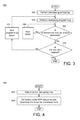
- FIG. 3 illustrates a flowchart for memory programming according to one embodiment of the present invention.
- FIG. 4 illustrates a flowchart of the interleaving scheduling according to one embodiment of the present invention.
- FIG. 5 illustrates a flowchart of the interleaving programming according to one embodiment of the present invention.
- FIG. 6 illustrates an example of a re-scheduled ISPP sequence according to one embodiment of the present invention.
- FIG. 7 illustrates another example of a re-scheduled ISPP sequence according to one embodiment of the present invention.
- FIG. 8A illustrates an exemplary resistance drift distribution based on the proposed interleaving programming technique.
- FIG. 8B illustrates an exemplary resistance drift distribution based on an original programming technique.
- FIG. 9 illustrates the calculated drift coefficients from the examples of FIGS. 8A and 8B .
- FIG. 1 illustrates a memory device 100 according to one embodiment of the present invention.
- the memory device 100 comprises a memory array 102 comprising a plurality of memory cells MC(1,1), MC(1,2) . . . , and MC(M,N) (referred to herein as memory cells MC), a row decoder 104 , a sense amplifier/data-in structure 106 , a column decoder 108 and a controller 110 .
- the memory cells can be phase change memory (PCM) cells or other types of cells.
- the row decoder 104 connects the memory cells MC via a plurality of word lines WL(1)-WL(M) (referred to herein as global bit lines WL).
- the row decoder 104 may select one of M rows of memory cells MC via the word lines WL.
- the sense amplifier/data-in structure 106 may detect data stored in the memory cells MC via bit lines BL(1)-BL(N) (referred to herein as global bit lines BL).
- the sense amplifier/data-in structure 106 includes current sources for the read, set, and reset modes, and is coupled to the column decoder 108 via the bit lines BL.
- the column decoder 108 connects the memory cells MC via the bit lines BL.
- the column decoder 108 may select one of N columns of memory cells MC via the bit lines BL.
- the controller 110 may control the row decoder 104 and column decoder 108 to perform program actions, verify actions, delay actions, or other actions.
- the memory device 100 may further comprise a look-up table (LUT) 112 for recording a plurality of parameters related to the resistance characteristics of the memory cells MC. The parameters stored in the LUT 112 can be provided to the controller 110 for optimal programming policy.
- LUT look-up table
- FIG. 2 illustrates an example of a normalized resistance characteristic of a memory cell MC.
- FIG. 3 illustrates a flowchart 300 for memory programming according to one embodiment of the present invention.
- the resistance of a memory cell MC may drift with time and can be modeled by the following exponential equation:
- R ⁇ ( t ) R 0 ⁇ ( t t 0 ) ⁇ ( eq1 )
- R 0 represents an initial resistance
- t 0 represents a reference time
- ⁇ represents a resistance drift coefficient
- the resistance characteristic curve of a memory cell MC can be divided into two regions: a rapid drift region RDR and a slow drift region SDR.
- the rapid drift region RDR and the slow drift region SDR can be distinguished by the tangent slope ( ⁇ r/ ⁇ t) of the resistance characteristic curve. For example, for a curve segment whose tangent slope is larger than a threshold, it can be regarded as being within the rapid drift region RDR; for a curve segment whose tangent slope is less than a threshold, it can be regarded as being within the slow drift region SDR.
- the amount of resistance change ( ⁇ r) per unit of time ( ⁇ t) of a memory cell MC in the rapid drift region RDR is larger than that in the slow drift region SDR.
- the curve 202 rises rapidly in the rapid drift region RDR while slowly in the slow drift region SDR. Since data stored in a memory cell MC is determined by its resistance value, data reliability may decrease when a memory cell MC is operated in its rapid drift region RDR.
- the controller 110 may perform interleaving scheduling to avoid the rapid drift region RDR (step 302 ). For example, based on the parameter stored in the LUT 112 , the controller 110 may adaptively re-arrange the action orders of Incremental Step Pulse Programming (ISPP) to ensure enough time elapse between each program action and its corresponding verify action.
- ISPP Incremental Step Pulse Programming
- the policy of the interleaving scheduling may consider the following conditions:
- the controller 110 may perform interleaving programming to control the row decoder 104 and the column decoder 108 to execute the scheduled program/verify/delay actions.
- the controller 110 may control the row decoder 104 and the column decoder 108 to:
- the controller 110 may check whether all scheduled memory cell actions (e.g., program/verify/delay actions) are performed. If no, step 308 is performed, and the next action is executed.
- all scheduled memory cell actions e.g., program/verify/delay actions
- the controller 110 may check whether all memory cells MC (or a target group of the memory cells MC, e.g., memory cells MC(1,1) to MC(1,n), where n is an integer less than N) are masked (step 310 ). If there is still remaining unmasked memory cell MC, step 312 is performed, and the next programming power is applied to the unmasked memory cells MC according to ISPP scheme.
- FIG. 4 illustrates a flowchart 400 of the interleaving scheduling according to one embodiment of the present invention.
- the controller 402 may determine an interleaving time for each target memory cell MC base on the abovementioned interleaving scheduling policy to avoid reading the target memory cells MC in their rapid drift regions RDR.
- the interleaving time may indicate a time elapse between a program action and its corresponding verify action.
- the interleaving time can be obtained by searching the LUT 112 which records a plurality of parameters associated with the resistance characteristics of the memory cells MC.
- the parameters may comprise, for example, at least one of temperature, program time, verify time, target interleaving time and delay time.
- the interleaving time can be obtained by performing one or more testing accesses on the memory cells MC.
- the controller 110 may read the memory cells MC to obtain resultant reading data, and modeling the resistance characteristics of the memory cells MC base on the resultant reading data to determine the interleaving time.
- the controller 110 may re-schedule the ISPP sequence base on the interleaving time and determine the action for the unmasked memory cell(s). For example, the controller 110 may determine how many dummy cycles, program actions, or verify actions should be inserted into the time elapse between a program action and its corresponding verify action according to the interleaving time. Based on the re-scheduled ISPP sequence, the actions for the unmasked memory cell(s) can then be determined.
- FIG. 5 illustrates a flowchart 500 of the interleaving programming according to one embodiment of the present invention.
- the interleaving programming includes executing the program/verify/delay actions of the re-scheduled ISPP sequence.
- the controller 110 first determines whether the current action for a target memory cell MC is verification or not (step 502 ). If yes, the controller 110 may verify the target memory cell MC. For example, the controller 110 may verify whether the cell metric (e.g., voltage, current, or resistance) of the target memory cell MC is within a target resistance range or not (step 504 ). If yes, the controller 110 then masks the target memory cell MC from the following actions (step 506 ).
- the cell metric e.g., voltage, current, or resistance
- step 508 the controller 110 checks whether the current action is programming or not (step 508 ). If yes, the controller 110 may program the target memory cell MC. For example, the controller 110 may look up the LUT 112 for a program condition (step 510 ) and program the target memory cell MC with a programming pulse (step 512 ). If not, the controller 110 may wait (delay) a dummy cycle T D to satisfy the interleaving scheduling policy (step 514 ).
- FIG. 6 illustrates an example of a re-scheduled ISPP sequence according to one embodiment of the present invention.
- D means the dummy cycle.
- the target group of memory cells includes k memory cells (e.g., MC(1,1) to MC(1,k), where k is an integer less than or equal to N).
- P(1,1) means the program action for the memory cell MC(1,1) at the first ISPP step
- P(2,1) means the program action for the memory cell MC(1,2) at the first ISPP step
- P(k ⁇ 1,1) means the program action for the memory cell MC(1,k ⁇ 1) at the first ISPP step
- P(k,1) means the program action for the memory cell MC(1,k) at the first ISPP step, etc.
- P(1,2) means the program action for the memory cell MC(1,1) at the second ISPP step
- P(2,2) means the program action for the memory cell MC(1,2) at the second ISPP step
- P(k ⁇ 1,2) means the program action for the memory cell MC(1,k ⁇ 1) at the second ISPP step
- P(k,2) means the program action for the memory cell MC(1,k) at the second ISPP step, etc.
- each program action has its corresponding verify action.
- V(1,1) which corresponds to the program action P(1,1), means the verify action for the memory cell MC(1,1) at the first ISPP step
- V(2,1) which corresponds to the program action P(2,1), means the verify action for the memory cell MC(1,2) at the first ISPP step
- V(k ⁇ 1,1) which corresponds to the program action P(k ⁇ 1,1), means the verify action for the memory cell MC(1,k ⁇ 1) at the first ISPP step
- V(k,1) which corresponds to the program action P(k,1), means the verify action for the memory cell MC(1,k) at the first ISPP step, etc.
- the program time for each program action is T P
- the verify time for each verify action is T V
- the delay time for each dummy cycle D is T D .
- each program action and its corresponding verify action can be regarded as being separated by a program action, except that the last program action and its corresponding verify action is separated by a dummy cycle D. As shown in FIG.
- the program action P(1,1) and its corresponding verify action V(1,1) is separated by the program action P(2,1); the program action P(2,1) and its corresponding verify action V(2,1) is separated by the program action P(3,1); the program action P(k ⁇ 1,1) and its corresponding verify action V(k ⁇ 1,1) is separated by the program action P(k,1); the program action P(k,1), which is the last program action at the first ISPP step, and its corresponding verify action V(k,1) is separated by a dummy cycle D.
- FIG. 7 illustrates another example of a re-scheduled ISPP sequence according to one embodiment of the present invention.
- the interleaving time for the target memory cells MC(1,1) to MC(1,k) is 3*T P .
- T P T V
- T P T D
- T k ′ 3 T D +3 T V ⁇ 3 T D ⁇ 3 T P (eq3)
- each program action and its corresponding verify action can be regarded as being separated by three program actions, except that the last program action (e.g., P(k,1)) and its corresponding verify action (i.e., V(k,1)) is separated by three dummy cycles D, as shown in FIG. 7 .
- the present invention is not limited to the above examples.
- the respective interleaving time for the target memory cells can be chosen according to practical needs and are unequal.
- the re-scheduled ISPP sequence may comprise an initial phase IP, a program & verify phase PV and a verify & dummy phase VD.
- the initial phase IP a portion of the target memory cells are sequentially programmed without performing verification. That is, program actions are performed sequentially without performing any verify actions in this phase IP.
- the number of program actions in the initial phase is determined by the interleaving time. As shown in FIG. 6 , two (1+programming pulses in the interleaving time) memory cells MC(1,1) and MC(1,2) are sequentially programmed (P(1,1) and P(2,1)) in the initial phase IP. Similarly, as shown in FIG. 7 , four (1+programming pulses in the interleaving time) memory cells MC(1,1) to MC(1,4) are sequentially programmed (P(1,1) to P(4,1)) in the initial phase IP.
- the program & verify phase PV can be regard as a mixture of program and verify actions.
- the program and verify actions are performed alternately in this phase PV.
- the verify action V(1,1), the program action P(3,1), the verify action (2,1), the program action (4,1), . . . , and the verify action V(k ⁇ 1,1) are performed alternately in the program & verify phase PV.
- the verify & dummy phase VD can be regard as a mixture of verify and delay actions. As shown in FIG. 6 , in the verify & dummy phase VD, the verify action V(k,1) follows shortly after the dummy cycle (delay action) D. In FIG. 7 , the dummy cycle D 1 , the verify action V(k ⁇ 2,1), the dummy cycle D 2 , the verify action V(k ⁇ 1,1), the dummy cycle D 3 and the verify action V(k,1) are performed alternately in this phase VD.
- FIG. 8A illustrates an exemplary resistance drift distribution based on the proposed interleaving programming technique.
- FIG. 8B illustrates an exemplary resistance drift distribution based on an original programming technique that each verify action follows immediately after its corresponding program action.
- the resistance drift distributions of FIGS. 8A and 8B are obtained after the same period of time (e.g., 100 seconds) and for the same number of memory cells (e.g., 256 memory cells).
- the interleaving programming technique enables tighter resistance drift distributions.
- FIG. 9 illustrates the calculated drift coefficients ( ⁇ ) from the examples of FIGS. 8A and 8B .
- the proposed interleaving programming technique can provide a 33% reduction in average drift coefficient and accordingly alleviate the resistance drift effect.
- the embodiments of the present invention can avoid reading the cell resistance in the rapid drift region by inserting actions between program actions and their corresponding verify action.
- the actions can be dummy cycles, interleaving program actions, interleaving verify actions, or other actions.
- the orders of an ISPP sequence can be re-scheduled with an appropriate interleaving time to obtain tighter resistance drift distributions. Therefore, resistance drift effects among the memory cells can be alleviated and the reliability of data reading can be improved.
Landscapes
- Chemical & Material Sciences (AREA)
- Crystallography & Structural Chemistry (AREA)
- Read Only Memory (AREA)
Abstract
Description
where the term R0 represents an initial resistance, the term t0 represents a reference time and the term γ represents a resistance drift coefficient.
T 1 =T P
T 2 =T P +T V ≈T P
.
.
.
T k−1 =T P +T V ≈T P
T k =T V +T D ≈T P (eq2)
T 1′=3T P
T 2′=3T P +T V≈3T P
.
.
.
T k−1 ′=T P+2T D +T V ≈T P+2T D≈3T P
T k′=3T D+3T V≈3T D≈3T P (eq3)
Claims (20)
Priority Applications (1)
| Application Number | Priority Date | Filing Date | Title |
|---|---|---|---|
| US14/687,998 US9478288B1 (en) | 2015-04-16 | 2015-04-16 | Method for programming memory device and associated memory device |
Applications Claiming Priority (1)
| Application Number | Priority Date | Filing Date | Title |
|---|---|---|---|
| US14/687,998 US9478288B1 (en) | 2015-04-16 | 2015-04-16 | Method for programming memory device and associated memory device |
Publications (2)
| Publication Number | Publication Date |
|---|---|
| US20160307627A1 US20160307627A1 (en) | 2016-10-20 |
| US9478288B1 true US9478288B1 (en) | 2016-10-25 |
Family
ID=57129885
Family Applications (1)
| Application Number | Title | Priority Date | Filing Date |
|---|---|---|---|
| US14/687,998 Active US9478288B1 (en) | 2015-04-16 | 2015-04-16 | Method for programming memory device and associated memory device |
Country Status (1)
| Country | Link |
|---|---|
| US (1) | US9478288B1 (en) |
Families Citing this family (3)
| Publication number | Priority date | Publication date | Assignee | Title |
|---|---|---|---|---|
| CN111951857B (en) * | 2019-05-15 | 2023-06-09 | 兆易创新科技集团股份有限公司 | Programming method and control device of nonvolatile memory |
| DE102020100541A1 (en) * | 2020-01-13 | 2021-07-15 | Infineon Technologies Ag | DETERMINATION OF A RESULTING DATA WORD WHEN ACCESSING A MEMORY |
| CN112071347B (en) * | 2020-09-08 | 2024-01-16 | 清华大学 | Operation method of resistive random access memory, control method of memory device and memory device |
Citations (3)
| Publication number | Priority date | Publication date | Assignee | Title |
|---|---|---|---|---|
| US20040240269A1 (en) * | 2001-09-17 | 2004-12-02 | Raul-Adrian Cernea | Latched programming of memory and method |
| US20080137409A1 (en) * | 2006-11-28 | 2008-06-12 | Kabushiki Kaisha Toshiba | Semiconductor memory device and method for erasing the same |
| US20090310421A1 (en) * | 2008-06-12 | 2009-12-17 | Raul-Adrian Cernea | Nonvolatile Memory with Correlated Multiple Pass Programming |
-
2015
- 2015-04-16 US US14/687,998 patent/US9478288B1/en active Active
Patent Citations (3)
| Publication number | Priority date | Publication date | Assignee | Title |
|---|---|---|---|---|
| US20040240269A1 (en) * | 2001-09-17 | 2004-12-02 | Raul-Adrian Cernea | Latched programming of memory and method |
| US20080137409A1 (en) * | 2006-11-28 | 2008-06-12 | Kabushiki Kaisha Toshiba | Semiconductor memory device and method for erasing the same |
| US20090310421A1 (en) * | 2008-06-12 | 2009-12-17 | Raul-Adrian Cernea | Nonvolatile Memory with Correlated Multiple Pass Programming |
Also Published As
| Publication number | Publication date |
|---|---|
| US20160307627A1 (en) | 2016-10-20 |
Similar Documents
| Publication | Publication Date | Title |
|---|---|---|
| US9196359B2 (en) | Read distribution management for phase change memory | |
| US7969786B2 (en) | Method of programming nonvolatile memory device | |
| JP5250117B2 (en) | Adaptive erase and soft programming for memory | |
| US7889566B2 (en) | Flash memory device, programming method thereof and memory system including the same | |
| US8879330B1 (en) | Non-volatile memory (NVM) with variable verify operations | |
| KR101184814B1 (en) | Nonvolatile memory device and program method of the same | |
| US9082503B2 (en) | Semiconductor memory device and method of operating the same | |
| JP2009283117A (en) | Method of programming nonvolatile memory device | |
| US8363471B2 (en) | Nonvolatile memory device and method of programming the same | |
| TW201027548A (en) | Nonvolatile memory and method with reduced program verify by ignoring fastest and/or slowest programming bits | |
| TW201308335A (en) | Intelligent shifting of read pass voltages for non-volatile storage | |
| KR20110048638A (en) | Method for programming semiconductor memory device | |
| TW201324512A (en) | Read compensation for partially programmed blocks of non-volatile storage | |
| TW200917272A (en) | Reducing the impact of interference during programming | |
| TW201103027A (en) | Forecasting program disturb in memory by detecting natural threshold voltage distribution | |
| US9053793B2 (en) | Semiconductor memory device and method of operating the same | |
| US9208875B2 (en) | Resistive nonvolatile memory device having cells programmed to achieve a target resistance value at a target time and writing method thereof | |
| US9478288B1 (en) | Method for programming memory device and associated memory device | |
| US9437311B1 (en) | Flash memory apparatus and initialization method for programming operation thereof | |
| JP2013137845A5 (en) | ||
| US9218887B2 (en) | Nonvolatile semiconductor memory device capable of improving retention/disturb characteristics of memory cells and method of operating the same | |
| TWI547947B (en) | Method for programming memory device and associated memory device | |
| KR20120005831A (en) | Memory device and method for operating the same | |
| CN106158030B (en) | Method and relevant memory device to memory device program | |
| KR20090105605A (en) | Method for pass voltage setting and method for programming of non volatile memory device |
Legal Events
| Date | Code | Title | Description |
|---|---|---|---|
| AS | Assignment |
Owner name: MACRONIX INTERNATIONAL CO., LTD., TAIWAN Free format text: ASSIGNMENT OF ASSIGNORS INTEREST;ASSIGNORS:KHWA, WIN-SAN;SU, TZU-HSIANG;WU, CHAO-I;AND OTHERS;REEL/FRAME:035421/0860 Effective date: 20150120 |
|
| STCF | Information on status: patent grant |
Free format text: PATENTED CASE |
|
| MAFP | Maintenance fee payment |
Free format text: PAYMENT OF MAINTENANCE FEE, 4TH YEAR, LARGE ENTITY (ORIGINAL EVENT CODE: M1551); ENTITY STATUS OF PATENT OWNER: LARGE ENTITY Year of fee payment: 4 |
|
| MAFP | Maintenance fee payment |
Free format text: PAYMENT OF MAINTENANCE FEE, 8TH YEAR, LARGE ENTITY (ORIGINAL EVENT CODE: M1552); ENTITY STATUS OF PATENT OWNER: LARGE ENTITY Year of fee payment: 8 |