US9191123B2 - Integrated circuits in optical receivers - Google Patents
Integrated circuits in optical receivers Download PDFInfo
- Publication number
- US9191123B2 US9191123B2 US14/642,651 US201514642651A US9191123B2 US 9191123 B2 US9191123 B2 US 9191123B2 US 201514642651 A US201514642651 A US 201514642651A US 9191123 B2 US9191123 B2 US 9191123B2
- Authority
- US
- United States
- Prior art keywords
- equalizer
- circuit
- signal
- optical
- integrated circuit
- Prior art date
- Legal status (The legal status is an assumption and is not a legal conclusion. Google has not performed a legal analysis and makes no representation as to the accuracy of the status listed.)
- Active
Links
Images


Classifications
-
- H—ELECTRICITY
- H04—ELECTRIC COMMUNICATION TECHNIQUE
- H04B—TRANSMISSION
- H04B10/00—Transmission systems employing electromagnetic waves other than radio-waves, e.g. infrared, visible or ultraviolet light, or employing corpuscular radiation, e.g. quantum communication
- H04B10/60—Receivers
- H04B10/61—Coherent receivers
- H04B10/616—Details of the electronic signal processing in coherent optical receivers
-
- H—ELECTRICITY
- H04—ELECTRIC COMMUNICATION TECHNIQUE
- H04B—TRANSMISSION
- H04B10/00—Transmission systems employing electromagnetic waves other than radio-waves, e.g. infrared, visible or ultraviolet light, or employing corpuscular radiation, e.g. quantum communication
- H04B10/60—Receivers
- H04B10/66—Non-coherent receivers, e.g. using direct detection
- H04B10/69—Electrical arrangements in the receiver
- H04B10/697—Arrangements for reducing noise and distortion
- H04B10/6971—Arrangements for reducing noise and distortion using equalisation
Definitions
- Optical systems use optical signals traveling through optical channels, such as optical fibers, to transmit data.
- optical channels such as optical fibers
- the frequency response of the optical signals may be altered.
- high frequency components of optical signals may be subject to more loss than low frequency components of optical signals.
- the loss of the high frequency components of optical signals may be caused by the optical fibers, the transmitters that generate the optical signals, among other components and factors. Loss of the high frequency components of optical signals within optical systems may reduce the ability of the optical systems to transmit data at higher speeds within proper error tolerances and may lead to data transmission failures within the optical systems.
- Some example embodiments generally relate to integrated circuits.
- a circuit may include a photodiode configured to receive an optical signal and convert the optical signal to a current signal.
- the circuit may also include a transimpedance amplifier coupled to the photodiode and configured to convert the current signal to a voltage signal.
- the circuit may also include an equalizer coupled to the transimpedance amplifier and configured to equalize the voltage signal to at least partially compensate for a loss of a high frequency component of the optical signal.
- the equalizer and the transimpedance amplifier may be housed within a single integrated circuit.
- an integrated circuit may include an input stage configured to receive a current signal from a photodiode and convert it to a voltage signal using a transimpedance amplifier.
- the current signal may represent an optical signal received by the photodiode.
- the integrated circuit may further include an equalizer coupled to the transimpedance amplifier and configured to equalize the voltage signal to at least partially compensate for a loss of a high frequency component of the optical signal.
- the integrated circuit may also include a driver configured to drive the equalized voltage signal from the integrated circuit to another integrated circuit.
- FIG. 1A is a block diagram of an example optical system that includes an integrated circuit
- FIG. 1B illustrates a graph of a frequency response of a voltage electrical signal within the optical system of FIG. 1A ;
- FIG. 2 is a block diagram of an example receiver that includes an integrated circuit
- FIG. 3 is a block diagram of an example equalizer
- FIG. 4A illustrates an example static equalizer
- FIG. 4B illustrates an example adjustable equalizer
- FIG. 5 is a block diagram of another example receiver that includes an integrated circuit
- FIG. 6 is a perspective view of an example optoelectronic module that may include an integrated circuit.
- the integrated circuit may include a transimpedance amplifier (TIA) and an equalizer circuit and may be part of an optical receiver circuit configured to convert an optical signal received over an optical channel into an electrical signal.
- TIA transimpedance amplifier
- equalizer circuit may be part of an optical receiver circuit configured to convert an optical signal received over an optical channel into an electrical signal.
- the TIA within the integrated circuit may be configured to convert a current signal generated by a photodiode based on a received optical signal into a voltage signal.
- the equalizer circuit may be configured to equalize the voltage signal to at least partially compensate for a loss of high frequency components of the received optical signal.
- a driver coupled to the TIA and the equalizer circuit for driving the equalized voltage signal to other circuits and/or integrated circuits, such as a clock and data recovery circuit may be non-linear. Allowing the driver to be non-linear may reduce the power used by the driver and thus the optical receiver circuit. Additionally or alternately, by equalizing the voltage signal generated by the TIA before driving the voltage signal to another circuit and/or integrated circuit allows the TIA to be decoupled from the other circuit and/or integrated circuit.
- Decoupling the TIA from another circuit and/or integrated circuit may allow for higher levels of interference between the TIA and the another circuit and/or integrated circuit than would be allowed if the voltage signal generated by the TIA was not equalized before sending the voltage signal to the another circuit and/or integrated circuit.
- FIG. 1A is a block diagram of an example optical system 100 that includes an integrated circuit 124 , arranged in accordance with at least some embodiments described herein.
- the optical system 100 may include, but is not limited to, a transmitter 110 , an optical channel 112 , a receiver 120 that includes the integrated circuit 124 , and a clock and data recovery circuit (CDR circuit) 130 .
- CDR circuit clock and data recovery circuit
- the transmitter 110 may be configured to generate an optical signal from an electrical signal and to transmit the optical signal through the optical channel 112 .
- the transmitter 110 may include an equalizer that may be configured to equalize the electrical signal before the electrical signal is converted into the optical signal.
- the transmitter 110 may equalize the electrical signal to assist in compensating for degradation of the optical signal as it travels through the optical channel 112 .
- the transmitter 110 may equalize the electrical signal to assist in compensating for degradation of the optical signal due to the transmitter 110 operating at a slower rate than the data rate of the electrical and optical signals.
- the optical channel 112 may be any channel configured to carry an optical signal.
- the optical channel 112 may be an optical fiber, such as a multi-mode optical fiber, or some other type of optical fiber.
- the properties of the optical channel 112 may result in degradation of the optical signal as the optical signal traverses the optical channel 112 .
- the optical channel 112 may affect the higher frequency components of the optical signal more than the lower frequency components of the optical signal. In these and other embodiments, the optical channel 112 may degrade the higher frequency components more than the lower frequency components.
- the receiver 120 may be coupled to the optical channel 112 and may be configured to receive the optical signal.
- the receiver 120 may also be configured to convert the optical signal to an electrical signal and to transmit the electrical signal to the CDR circuit 130 .
- the receiver 120 may be configured to convert the optical signal to a current electrical signal and then convert the current electrical signal to a voltage signal that is transmitted to the CDR circuit 130 .
- the receiver 120 may convert the optical signal to the current electrical signal using a photodiode or some other optical to electrical converter. After converting the optical signal to the current electrical signal, the integrated circuit 124 may convert the current electrical signal to a voltage electrical signal. The integrated circuit 124 may also equalize the voltage electrical signal to at least partially compensate for the degradation of higher frequency components of the optical signal that occur due to limitations, defects, or other aspects of the transmitter 110 and/or the optical channel 112 . After the integrated circuit 124 converts the optical signal into a voltage electrical signal and equalizes the voltage electrical signal, the integrated circuit 124 may send the equalized voltage electrical signal to the CDR circuit 130 .
- the integrated circuit 124 may house circuitry to both convert a current electrical signal into a voltage electrical signal and to equalize the voltage electrical signal.
- the power used by the optical system 100 may be reduced as compared to optical systems that equalize voltage electrical signals in a CDR circuit or some other circuit besides the circuit that converts the current electrical signal to the voltage electrical signal.
- the power used by the optical system 100 may be reduced because the voltage electrical signal may be transmitted to the CDR circuit 130 from the receiver 120 using non-linear drivers instead of linear drivers.
- Non-linear drivers may be used because the non-linear effects that affected the optical signal during creation and/or transmission of the optical signal have already been accounted for by the integrated circuit 124 by equalizing the voltage electrical signal.
- equalizing the voltage electrical signal allows the receiver 120 to be decoupled from the CDR circuit 130 .
- equalizing the voltage electrical signal may allow for higher levels of interference between the receiver 120 and the CDR circuit 130 without causing unacceptable loss of the equalized voltage electrical signal transmitted to the CDR circuit 130 from the receiver 120 .
- the receiver 120 may send the equalized voltage electrical signal to another circuit other than the CDR circuit 130 .
- FIG. 1B illustrates a graph 150 of a frequency response of a voltage electrical signal within the optical system 100 of FIG. 1A , arranged in accordance with at least some embodiments described herein.
- the graph 150 has an x-axis that represents a frequency of various frequency components of a voltage electrical signal.
- the y-axis of the graph 150 represents a magnitude of the frequency components of the voltage electrical signal.
- the graph contains a line 160 and a dashed line 170 .
- the line 160 indicates a magnitude of different frequency components of the voltage electrical signal after the voltage electrical signal is derived from an optical signal that passes through the optical system 100 . As illustrated by the line 160 , the magnitudes of the higher frequency components of the voltage electrical signal are attenuated more than the magnitudes of the lower frequency components of the voltage electrical signal. Examples of higher frequency components that may have reduced magnitudes include frequency components having frequencies above a few GHz.
- the dashed line 170 indicates a magnitude of different frequency components of the voltage electrical signal after the voltage electrical signal is derived from an optical signal that passes through the optical system 100 and is equalized by the integrated circuit 124 . As illustrated by the dashed line 170 , the magnitudes of the higher frequency components of the voltage electrical signal are increased as compared to the magnitudes of the higher frequency components of the voltage electrical signal without equalization.
- FIG. 2 is a block diagram of an example receiver 200 that includes an integrated circuit 210 , arranged in accordance with at least some embodiments described herein.
- the receiver 200 may include, but is not limited to, a photodiode 214 coupled to the integrated circuit 210 .
- the integrated circuit 210 may include a transimpedance amplifier (TIA) 220 , an equalizer 230 , a driver 240 , an input port 215 , a communication port 216 , and an output port 218 .
- TIA transimpedance amplifier
- FIG. 2 further illustrates an optical fiber 212 adjacent to the photodiode 214 .
- the optical fiber 212 may be any type of optical fiber, such as a multi-mode fiber, that is configured to transmit an optical signal.
- the photodiode 214 may be configured to receive an optical signal from the optical fiber 212 .
- the photodiode 214 may also be configured to convert the received optical signal into a current electrical signal and to send the current electrical signal to the input port 215 of the integrated circuit 210 .
- the TIA 220 may be configured to receive the current electrical signal from the input port 215 and to convert the current electrical signal into a voltage electrical signal. In some embodiments, the TIA 220 may also amplify the voltage electrical signal. In some embodiments, the TIA 220 may have a linear response or an approximate linear response. Thus, the TIA 220 may have no or a marginally different effect on different frequency components of the voltage electrical signal. Thus, differences in magnitudes between frequency components may be marginally maintained. The TIA 220 may send the voltage electrical signal to the equalizer 230 .
- the equalizer 230 may be configured to equalize the voltage electrical signal. To equalize the voltage electrical signal, the equalizer 230 may adjust the magnitude of certain frequency components of the voltage electrical signal to reduce differences between magnitudes of frequency components of the voltage electrical signal. For example, if higher frequency components of the voltage electrical signal had lower magnitudes than lower frequency components, the equalizer 230 may reduce the magnitude of lower frequency components, increase the magnitude of higher frequency components, or some combination thereof, to reduce the differences between the magnitudes of the frequency components. Equalizing the voltage electrical signal may reduce intersymbol interference of a data signal transmitted on the optical signal through the optical fiber 212 . Reducing intersymbol interference may allow for better recovery of the data signal. The equalizer 230 may send the equalized voltage electrical signal to the driver 240 .
- the equalizer 230 may be a linear equalizer, such as a continuous time linear equalizer or a linear feed forward equalizer. Alternately or additionally, the equalizer 230 may be a static equalizer, an adjustable equalizer, or a combination thereof.
- a static equalizer may adjust the magnitude of one or more frequency components of a signal in a consistent manner.
- An adjustable equalizer may adjust the magnitude of one or more frequency components of a signal based on a setting within the adjustable equalizer that may be adjusted based on an input.
- the communication port 216 may be configured to receive an indication from an outside source of the frequency components of a voltage electrical signal whose magnitudes are affected and/or how much the magnitudes are affected.
- the equalizer 230 may adjust the equalization of the voltage electrical signal.
- the communication port 216 may be any type of communication port, such as a serial port or a parallel port.
- the communication port 216 is a serial port, the integrated circuit 210 may interface with an outside source using any one of numerous serial communication protocols, such as, but not limited to, I 2 C, SPI, serial ATA, FireWire, PCI, PCI express, among others.
- the communication port 216 is a parallel port
- the integrated circuit 210 may interface with an outside source using any one of numerous parallel communication protocols, such as, but not limited to ISA, parallel ATA, SCSI, among others.
- the driver 240 may receive the equalized voltage electrical signal from the equalizer 230 and driver the equalized voltage electrical signal out the output port 218 to another circuit, such as an another integrated circuit.
- the driver 240 may drive the equalized voltage electrical signal to a CDR circuit.
- the driver 240 may have a non-linear response.
- the driver 240 having a non-linear response as compared to a linear response may reduce the power consumption of the driver 240 and subsequently the power consumption of the integrated circuit 210 .
- the driver 240 may have a non-linear response because the voltage electrical signal is equalized by the equalizer 230 before being driven by the driver 240 .
- a driver of the receiver may have a linear or substantially linear response to minimize changes to a voltage electrical signal; to thereby decrease errors in a data signal extracted from the voltage electrical signal.
- the receiver 200 may include an optical to electrical converter besides a photodiode.
- the integrated circuit 210 may not include the driver 240 .
- the TIA 220 and the equalizer 230 may form the integrated circuit 210 and the driver 240 may be a separate component.
- the integrated circuit 230 may not include the communication port 216 .
- the equalizer 230 may be a static equalizer.
- FIG. 3 is a block diagram of an example equalizer 300 , arranged in accordance with at least some embodiments described herein.
- the equalizer 300 may include, but is not limited to, a static portion and an adjustable portion.
- the static portion may include a static equalizer unit 310 and the adjustable portion may include an adjustable equalizer unit 320 .
- the equalizer 300 may be configured to receive a signal and provide equalization among frequency components of the signal.
- the static equalizer unit 310 may be configured to provide constant equalization of a signal received by the equalizer 300 .
- Providing constant equalization may include the static equalizer unit 310 adjusting magnitudes of set frequency components of the signal by a predetermined amount.
- the static equalizer unit 310 may increase the magnitude of frequency components of a signal above 5 GHz by 20 dB.
- the static equalizer unit 310 may be a digital equalizer or an analog equalizer.
- the adjustable equalizer unit 320 may be configured to provide adjustable equalization of a signal received by the equalizer 300 .
- Providing adjustable equalization may include the adjustable equalizer unit 320 adjusting the magnitudes of set frequency components of the signal by an adjustable amount, adjusting the magnitude of adjustable frequency components of the signal by a set amount, or some combination thereof.
- the adjustable equalizer unit 320 may increase a magnitude of frequency components of a signal above 5 GHz by 20 dB and then may be adjusted to increase the magnitude of the frequency components of the signal above 5 GHz by 10 dB.
- the adjustable equalizer unit 320 may increase a magnitude of frequency components of a signal above 5 GHz by 20 dB and then may be adjusted to increase the magnitude of the frequency components of the signal above 7 GHz by 20 dB.
- the adjustable equalizer unit 320 may be a digital equalizer or an analog equalizer. The adjustable equalizer unit 320 may be adjusted based on an input received through a communication port 322 in the equalizer 300 .
- the equalizer 300 may be incorporated into a single integrated circuit with other components, such as a TIA.
- the equalizer 300 may be used in place of the equalizer 230 of FIG. 2 .
- the equalizer 300 may be part of the IC 124 of FIG. 1A .
- the equalizer 300 may include multiple static equalizers or multiple adjustable equalizers. Alternately or additionally, the equalizer 300 may not include the static equalizer unit 310 or the adjustable equalizer unit 320 .
- FIG. 4A illustrates an example static equalizer 400 A, arranged in accordance with at least some embodiments described herein.
- the static equalizer 400 A may include, but is not limited to, resistors 402 and 404 and capacitor 406 .
- the resistors 402 and 404 may form a resistive divider, with the resistor 402 coupled to an input and an output of the static equalizer 400 A and the resistor 404 coupled between the output and ground.
- the capacitor 406 may be coupled across the resistor 402 between the input and the output.
- the static equalizer 400 A may operate as a resistive divider of lower frequency components of a signal thereby reducing the magnitude of lower frequency components. Higher frequency components of the static equalizer 400 A may pass by the resistor divider by way of the capacitor 406 .
- the static equalizer 400 A may thus equalize a signal by reducing a magnitude of lower frequency components to be similar in magnitude to higher frequency components.
- the amount of reduction in magnitude and the higher frequencies that may pass without having a reduction in magnitude may be selected based on the values of the resistors 402 and 404 and the capacitor 406 .
- Modifications, additions, or omissions may be made to the static equalizer 400 A without departing from the scope of the present disclosure.
- additional active and/or passive circuit elements may be included in the static equalizer 400 A.
- FIG. 4B illustrates an example adjustable equalizer 400 B, arranged in accordance with at least some embodiments described herein.
- the adjustable equalizer 400 B may be configured to equalize a signal based on a selected value for one or more adjustable values.
- the adjustable equalizer 400 B may include, but is not limited to, adjustable gain blocks 410 , 412 , and 414 , delay blocks 420 and 422 , and a summer 430 .
- the delay blocks 420 and 422 may have the same delay or varying delays.
- the adjustable gain blocks 410 , 412 , and 414 may each be adjusted to increase and/or decrease a magnitude of a signal or a delayed portion of the signal.
- the adjustable gain block 410 may have a gain of 1 ⁇ 2 and thus decrease a magnitude of a signal and the adjustable gain block 412 may have a gain of 2 and thus increase a magnitude of the signal or a delayed portion of the signal.
- a signal at an input of the adjustable equalizer 400 B may be sent to the gain block 410 and the delay block 420 .
- the gain block 410 may adjust a magnitude of the signal and may send the adjusted signal to the summer 430 .
- the delay block 420 may delay the signal.
- a magnitude of the delayed signal may be adjusted by the gain block 412 .
- the adjusted delayed signal from the gain block 412 may be sent to the summer 430 .
- the delay block 422 may further delay the delayed signal and may send the twice-delayed signal to the gain block 414 .
- the gain block 414 may adjust a magnitude of the twice-delayed signal and may send the adjusted twice-delayed signal to the summer 430 .
- the summer 430 may sum the adjusted signal, the adjusted delayed signal, and the adjusted twice-delayed signal and may output the result on an output of the adjustable equalizer 400 B.
- the adjustable equalizer 400 B may equalize a signal by increasing a magnitude of higher frequency components of a signal to be more similar to a magnitude of lower frequency components. Modifications, additions, or omissions may be made to the adjustable equalizer 400 B without departing from the scope of the present disclosure.
- the adjustable equalizer 400 B may be configured with an additional delay block and gain block.
- the adjustable equalizer 400 B may be configured with a feedback loop and a gain block.
- FIG. 5 is a block diagram of another example receiver 500 that includes an integrated circuit 510 , arranged in accordance with at least some embodiments described herein.
- the receiver 500 may include, but is not limited to, a photodiode 514 coupled to the integrated circuit 510 .
- the integrated circuit 510 may include a TIA 520 , an equalizer 530 , a driver 540 , an input port 515 , a communication port 516 , and an output port 518 .
- FIG. 5 further illustrates an optical fiber 512 adjacent to the photodiode 514 .
- the optical fiber 512 may be any type of optical fiber, such as a multi-mode fiber, that is configured to transmit an optical signal.
- the photodiode 514 may be configured to receive an optical signal from the optical fiber 512 .
- the photodiode 514 may also be configured to convert the optical signal into a current electrical signal and to send the current electrical signal to the input port 515 of the integrated circuit 510 .
- the TIA 520 may be configured to receive the current electrical signal from the input port 515 and to convert the current electrical signal into a pair of differential voltage electrical signals.
- the TIA 520 may include a first amplifier 522 and a first resistor 521 that may be configured to convert the current electrical signal from the photodiode 514 into a first voltage signal of the pair of differential voltage electrical signals.
- the TIA 520 may also include a capacitor 525 , a second amplifier 523 , and a second resistor 524 that may be configured to generate a second voltage signal of the pair of differential voltage electrical signals based on the current signal and/or the first voltage signal.
- the first and second voltage signals may be amplified by an amplifier 528 and sent to the equalizer 530 .
- the TIA 520 may have a linear response or an approximate linear response. Thus, the TIA 520 may have no or a marginally different effect on different frequency components of the pair of differential voltage electrical signals. Thus, differences in magnitudes between frequency components may be marginally maintained.
- the equalizer 530 may be configured to equalize the pair of differential voltage electrical signals.
- the equalizer 500 may include, but is not limited to, a static portion and an adjustable portion.
- the static portion may include a static equalizer unit 534 and the adjustable portion may include an adjustable equalizer unit 532 .
- the static equalizer unit 534 may be configured to equalize the pair of differential voltage electrical signals by adjusting a magnitude of set frequency components of the pair of differential voltage electrical signals by a predetermined amount.
- the static equalizer unit 534 may decrease or increase the magnitude of higher or lower frequency components of the pair of differential voltage electrical signals to equalize the pair of differential voltage electrical signals.
- the adjustable equalizer unit 532 may be configured to provide adjustable equalization of the pair of differential voltage electrical signals. In some embodiments, an amount of equalization provided by the adjustable equalizer unit 532 may be determined based on an input received through the communication port 516 . In some embodiments, the adjustable equalizer unit 532 may be configured to further reduce and/or increase high or low frequency components of the pair of differential voltage electrical signals based on the equalization performed by the static equalizer unit 534 . Alternately or additionally, the adjustable equalizer unit 532 may be configured to reduce a magnitude of a frequency component whose magnitude is increased by the static equalizer unit 534 or increase a magnitude of a frequency component whose magnitude is decreased by the static equalizer unit 534 .
- the adjustable equalizer unit 532 may be used to provide finer tuned equalization of the pair of differential voltage electrical signals.
- the static and the adjustable equalizer units 534 and 532 may be linear equalizers. Alternately or additionally, the static and the adjustable equalizer units 534 and 532 may be digital equalizers, analog equalizers, or some combination thereof.
- the equalizer 530 may send the equalized pair of differential voltage electrical signals to the driver 540 .
- the driver 540 may receive the equalized pair of differential voltage electrical signals from the equalizer 530 and driver the equalized pair of differential voltage electrical signals out the output port 218 to another circuit, such as an another integrated circuit.
- the driver 540 may drive the equalized pair of differential voltage electrical signals to a CDR circuit.
- the driver 540 may have a non-linear response.
- the integrated circuit 510 may not include the driver 540 .
- the TIA 520 and the equalizer 530 may form the integrated circuit 510 and the driver 540 may be a separate component.
- the TIA 520 may include additional active and/or passive circuit elements.
- the equalizer 530 may include additional static or adjustable equalizer units or may not include either the static equalizer unit 534 or the adjustable equalizer unit 532 .
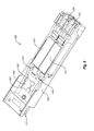
- FIG. 6 is a perspective view of an example optoelectronic module 600 (hereinafter “module 600 ”) that may include an integrated circuit 620 , arranged in accordance with at least some embodiments described herein.
- the module 600 may be configured for use in transmitting and receiving optical signals in connection with a host device (not shown).
- the module 600 may include, but is not limited to, a bottom housing 602 ; a receive port 604 and a transmit port 606 , both defined in the bottom housing 602 ; a PCB 608 positioned within the bottom housing 602 , the PCB 608 having the integrated circuit 620 and a second integrated circuit 622 positioned hereon; and a receiver optical subassembly (ROSA) 610 and a transmitter optical subassembly (TOSA) 612 also positioned within the bottom housing 602 .
- An edge connector 614 may be located on an end of the PCB 608 to enable the module 600 to electrically interface with the host device. As such, the PCB 608 facilitates electrical communication between the host device and the ROSA 610 and TOSA 612 .
- the module 600 may be configured for optical signal transmission and reception at a variety of data rates including, but not limited to, 1 Gb/s, 10 Gb/s, 20 Gb/s, 40 Gb/s, 100 Gb/s, or higher. Furthermore, the module 600 may be configured for optical signal transmission and reception at various distinct wavelengths using wavelength division multiplexing (WDM) using one of various WDM schemes, such as Coarse WDM, Dense WDM, or Light WDM. Furthermore, the module 600 may be configured to support various communication protocols including, but not limited to, Fibre Channel and High Speed Ethernet. In addition, although illustrated in a particular form factor in FIG.
- WDM wavelength division multiplexing
- the module 600 may be configured in any of a variety of different form factors including, but not limited to, the Small Form-factor Pluggable (SFP), the enhanced Small Form-factor Pluggable (SFP+), the 10 Gigabit Small Form Factor Pluggable (XFP), the C Form-factor Pluggable (CFP) and the Quad Small Form-factor Pluggable (QSFP) multi-source agreements (MSAs).
- SFP Small Form-factor Pluggable
- SFP+ enhanced Small Form-factor Pluggable
- XFP 10 Gigabit Small Form Factor Pluggable
- CFP C Form-factor Pluggable
- QSFP Quad Small Form-factor Pluggable multi-source agreements
- the ROSA 610 may house one or more optical receivers, such as photodiodes, that are electrically coupled to an electrical interface 616 .
- the one or more optical receivers may be configured to convert optical signals received through the receive port 604 into corresponding current electrical signals that are relayed to the integrated circuit 620 through the electrical interface 616 and the PCB 608 .
- the TOSA 612 may house one or more optical transmitters, such as lasers, that are electrically coupled to another electrical interface 618 .
- the one or more optical transmitters may be configured to convert electrical signals received from a host device by way of the PCB 608 and the electrical interface 618 into corresponding optical signals that are transmitted through the transmit port 606 .
- the integrated circuit 620 which may be similar to and/or correspond to the integrated circuits 124 , 210 , or 510 of FIG. 1 , 2 , or 5 respectively, may be configured to convert the current electrical signals to voltage electrical signals and to equalize the voltage electrical signals.
- the integrated circuit 620 may drive the equalized voltage electrical signals to the second integrated circuit 622 .
- the second integrated circuit may be a CDR circuit.
- an integrated circuit such as the integrated circuits 124 , 210 , or 510 of FIG. 1 , 2 , or 5 respectively may be incorporated into the ROSA 610 and may be used to convert current electrical signals to equalized voltage electrical signals. Modifications, additions, or omissions may be made to the module 600 without departing from the scope of the present disclosure.
- the module 600 illustrated in FIG. 6 is one architecture in which embodiments of the present disclosure may be employed. This specific architecture is only one of countless architectures in which embodiments may be employed. The scope of the present disclosure is not intended to be limited to any particular architecture or environment.
Landscapes
- Physics & Mathematics (AREA)
- Electromagnetism (AREA)
- Engineering & Computer Science (AREA)
- Computer Networks & Wireless Communication (AREA)
- Signal Processing (AREA)
- Amplifiers (AREA)
- Optical Communication System (AREA)
Abstract
Description
Claims (16)
Priority Applications (1)
| Application Number | Priority Date | Filing Date | Title |
|---|---|---|---|
| US14/642,651 US9191123B2 (en) | 2012-10-29 | 2015-03-09 | Integrated circuits in optical receivers |
Applications Claiming Priority (2)
| Application Number | Priority Date | Filing Date | Title |
|---|---|---|---|
| US13/663,056 US8977139B2 (en) | 2012-10-29 | 2012-10-29 | Integrated circuits in optical receivers |
| US14/642,651 US9191123B2 (en) | 2012-10-29 | 2015-03-09 | Integrated circuits in optical receivers |
Related Parent Applications (1)
| Application Number | Title | Priority Date | Filing Date |
|---|---|---|---|
| US13/663,056 Continuation US8977139B2 (en) | 2012-10-29 | 2012-10-29 | Integrated circuits in optical receivers |
Publications (2)
| Publication Number | Publication Date |
|---|---|
| US20150180587A1 US20150180587A1 (en) | 2015-06-25 |
| US9191123B2 true US9191123B2 (en) | 2015-11-17 |
Family
ID=50547303
Family Applications (2)
| Application Number | Title | Priority Date | Filing Date |
|---|---|---|---|
| US13/663,056 Active 2033-05-24 US8977139B2 (en) | 2012-10-29 | 2012-10-29 | Integrated circuits in optical receivers |
| US14/642,651 Active US9191123B2 (en) | 2012-10-29 | 2015-03-09 | Integrated circuits in optical receivers |
Family Applications Before (1)
| Application Number | Title | Priority Date | Filing Date |
|---|---|---|---|
| US13/663,056 Active 2033-05-24 US8977139B2 (en) | 2012-10-29 | 2012-10-29 | Integrated circuits in optical receivers |
Country Status (7)
| Country | Link |
|---|---|
| US (2) | US8977139B2 (en) |
| EP (1) | EP2912787B1 (en) |
| JP (3) | JP2015537445A (en) |
| KR (1) | KR101725878B1 (en) |
| CN (1) | CN104871456B (en) |
| CA (1) | CA2889966C (en) |
| WO (1) | WO2014070675A1 (en) |
Cited By (3)
| Publication number | Priority date | Publication date | Assignee | Title |
|---|---|---|---|---|
| US9866184B1 (en) | 2016-09-28 | 2018-01-09 | International Business Machines Corporation | Degenerated transimpedance amplifier with wire-bonded photodiode for reducing group delay distortion |
| US11272877B2 (en) | 2013-10-15 | 2022-03-15 | Autonomix Medical, Inc. | Systems and methods for treating cancer and/or augmenting organ function |
| US11382687B2 (en) | 2013-10-15 | 2022-07-12 | Autonomix Medical, Inc. | Systems and methods for treating cancer and/or augmenting organ function |
Families Citing this family (17)
| Publication number | Priority date | Publication date | Assignee | Title |
|---|---|---|---|---|
| US8977139B2 (en) * | 2012-10-29 | 2015-03-10 | Finisar Corporation | Integrated circuits in optical receivers |
| US11133866B2 (en) | 2014-02-25 | 2021-09-28 | Pharmaseq, Inc. | All optical identification and sensor system with power on discovery |
| WO2016008078A1 (en) * | 2014-07-14 | 2016-01-21 | 华为技术有限公司 | Control circuit for equalizer, equalizer and optical receiver |
| US10882258B1 (en) | 2016-01-22 | 2021-01-05 | Pharmaseq, Inc. | Microchip affixing probe and method of use |
| CN106788776A (en) * | 2016-12-20 | 2017-05-31 | 中国科学院半导体研究所 | A kind of photodetector and opto-electronic conversion method |
| KR20200041177A (en) | 2018-10-11 | 2020-04-21 | 전자부품연구원 | Optical receiver for real-time monitoring |
| CN111224718B (en) * | 2018-11-23 | 2023-06-20 | 阿里巴巴集团控股有限公司 | Optical module and optical module signal processing method |
| US10826729B1 (en) * | 2019-07-19 | 2020-11-03 | Eagle Technology, Llc | Communication system with adjustable equalization levels and related methods |
| CN110515874B (en) * | 2019-09-11 | 2021-06-29 | 上海兆芯集成电路有限公司 | Drive system |
| TW202143665A (en) | 2020-01-10 | 2021-11-16 | 美商Macom技術方案控股公司 | Optimal equalization partitioning |
| US11575437B2 (en) | 2020-01-10 | 2023-02-07 | Macom Technology Solutions Holdings, Inc. | Optimal equalization partitioning |
| JP2023522540A (en) | 2020-02-14 | 2023-05-31 | ピー-チップ・アイピー・ホールディングス・インコーポレイテッド | optical trigger transponder |
| US11233353B2 (en) * | 2020-05-05 | 2022-01-25 | Jabil Inc. | Method, system, and apparatus for finely pitched high speed connector attachment |
| US11539555B2 (en) | 2020-06-29 | 2022-12-27 | Texas Instruments Incorporated | Enhanced discrete-time feedforward equalizer |
| US11743080B2 (en) * | 2020-06-29 | 2023-08-29 | Texas Instruments Incorporated | Sample-and-hold-based retimer supporting link training |
| CN114095092A (en) * | 2022-01-21 | 2022-02-25 | 微龛(广州)半导体有限公司 | Optical receiving module and equalization compensation method |
| CN115001591B (en) * | 2022-05-25 | 2023-08-04 | 西安交通大学 | High-speed analog multiplexer for coherent light detection of more than 100G |
Citations (11)
| Publication number | Priority date | Publication date | Assignee | Title |
|---|---|---|---|---|
| US20030067662A1 (en) | 2001-10-09 | 2003-04-10 | Tony M. Brewer | Fast decision threshold controller for burst-mode receiver |
| US20080240737A1 (en) | 2007-03-28 | 2008-10-02 | Fujitsu Limited | Optical receiver and control method for optical receiver |
| KR100958218B1 (en) | 2002-03-22 | 2010-05-18 | 멜렉시스 게엠베하 | Optical fiber receiver having an increased bandwidth |
| US7902900B2 (en) * | 2006-07-21 | 2011-03-08 | Mediatek Inc. | Limiting amplifiers |
| US20110135316A1 (en) | 2009-12-07 | 2011-06-09 | Eric Fankhauser | Electrical-optical media conversion system |
| US20120045202A1 (en) | 2010-08-17 | 2012-02-23 | Xu Jiang | High Speed Bi-Directional Transceiver, Circuits and Devices Therefor, and Method(s) of Using the Same |
| US20130188965A1 (en) * | 2012-01-23 | 2013-07-25 | Gil Afriat | Optical transceiver with equalization and controllable laser interconnection interface |
| US20130229236A1 (en) * | 2011-03-02 | 2013-09-05 | International Business Machines Corporation | Optical receiver based on a decision feedback equalizer |
| US20130302028A1 (en) * | 2009-12-08 | 2013-11-14 | Vello Systems, Inc. | Optical Subchannel Routing, Protection Switching and Security |
| US20140023376A1 (en) * | 2009-11-09 | 2014-01-23 | Quantum Electro Opto Systems Sdn. Bhd. | High Speed Communication |
| US8977139B2 (en) * | 2012-10-29 | 2015-03-10 | Finisar Corporation | Integrated circuits in optical receivers |
Family Cites Families (25)
| Publication number | Priority date | Publication date | Assignee | Title |
|---|---|---|---|---|
| JPS5286702A (en) * | 1976-01-14 | 1977-07-19 | Hitachi Ltd | Automatic equalizer system |
| US4565974A (en) * | 1984-08-13 | 1986-01-21 | At&T Bell Laboratories | Optical receiver circuit with active equalizer |
| JP2503837B2 (en) * | 1992-07-16 | 1996-06-05 | 日本電気株式会社 | Digital optical receiver circuit and preamplifier circuit in digital optical receiver circuit |
| JPH06232647A (en) * | 1993-01-29 | 1994-08-19 | Sumitomo Electric Ind Ltd | Optical reception circuit |
| JPH08223228A (en) * | 1994-03-17 | 1996-08-30 | Fujitsu Ltd | Equalization amplifier and receiver and preamplifier using same |
| CN2269676Y (en) * | 1996-11-29 | 1997-12-03 | 邮电部激光通信研究所 | Optical fiber transmission equipment for mobile communication direct broadcast station |
| JP2000201031A (en) * | 1999-01-07 | 2000-07-18 | Nec Miyagi Ltd | Light receiving circuit |
| EP1447950A1 (en) * | 2003-02-14 | 2004-08-18 | Vrije Universiteit Brussel | Low voltage adaptive equalizer |
| CN1842859A (en) * | 2003-08-27 | 2006-10-04 | 皇家飞利浦电子股份有限公司 | Read equalizer for a data storage system |
| US7532820B2 (en) * | 2004-10-29 | 2009-05-12 | Finisar Corporation | Systems and methods for providing diagnostic information using EDC transceivers |
| KR100682993B1 (en) * | 2004-12-13 | 2007-02-15 | 한국전자통신연구원 | Optical Receiving Apparatus using transformer |
| US20070154147A1 (en) * | 2005-12-29 | 2007-07-05 | Weem Jan P P | Mechanism to increase an optical link distance |
| US20080106643A1 (en) * | 2006-11-08 | 2008-05-08 | Rgb Systems, Inc. | Method and apparatus for video transmission over long distances using twisted pair cables |
| US8231284B2 (en) * | 2007-03-26 | 2012-07-31 | International Business Machines Corporation | Ultra-high bandwidth, multiple-channel full-duplex, single-chip CMOS optical transceiver |
| US20080267633A1 (en) * | 2007-04-26 | 2008-10-30 | Intel Corporation | Split equalization function for optical and electrical modules |
| JP5029200B2 (en) * | 2007-08-03 | 2012-09-19 | 住友電気工業株式会社 | Optical transceiver adjustment method |
| JP5081678B2 (en) * | 2008-03-24 | 2012-11-28 | 株式会社日立製作所 | Optical signal receiving circuit |
| US8374231B2 (en) * | 2008-04-30 | 2013-02-12 | Tektronix, Inc. | Equalization simulator with training sequence detection for an oscilloscope |
| JP5042925B2 (en) * | 2008-06-10 | 2012-10-03 | 日本電信電話株式会社 | Waveform equalizer and receiver and optical transmission system |
| US8150273B2 (en) * | 2008-09-04 | 2012-04-03 | Finisar Corporation | Optical receiver with threshold voltage compensation |
| KR101048019B1 (en) * | 2009-08-14 | 2011-07-13 | 이화여자대학교 산학협력단 | High Speed Single Chip CMOS Optical Receiver |
| JP2011060369A (en) * | 2009-09-09 | 2011-03-24 | Panasonic Corp | Filter coefficient control apparatus |
| US9048954B2 (en) * | 2011-03-02 | 2015-06-02 | International Business Machines Corporation | Optical interconnect using optical transmitter pre-distortion |
| CN102412897B (en) * | 2011-08-17 | 2014-12-10 | 索尔思光电(成都)有限公司 | Single-fiber four-way symmetrical optical module |
| CN202738007U (en) * | 2012-06-27 | 2013-02-13 | 成都微迪数字系统技术有限公司 | Optical transmitter and optical receiver |
-
2012
- 2012-10-29 US US13/663,056 patent/US8977139B2/en active Active
-
2013
- 2013-10-28 EP EP13851434.4A patent/EP2912787B1/en not_active Not-in-force
- 2013-10-28 CA CA2889966A patent/CA2889966C/en not_active Expired - Fee Related
- 2013-10-28 CN CN201380068116.2A patent/CN104871456B/en not_active Expired - Fee Related
- 2013-10-28 WO PCT/US2013/067130 patent/WO2014070675A1/en active Application Filing
- 2013-10-28 KR KR1020157014278A patent/KR101725878B1/en active IP Right Grant
- 2013-10-28 JP JP2015539887A patent/JP2015537445A/en active Pending
-
2015
- 2015-03-09 US US14/642,651 patent/US9191123B2/en active Active
-
2017
- 2017-11-15 JP JP2017220080A patent/JP2018026880A/en active Pending
-
2020
- 2020-01-31 JP JP2020014273A patent/JP2020092430A/en not_active Withdrawn
Patent Citations (11)
| Publication number | Priority date | Publication date | Assignee | Title |
|---|---|---|---|---|
| US20030067662A1 (en) | 2001-10-09 | 2003-04-10 | Tony M. Brewer | Fast decision threshold controller for burst-mode receiver |
| KR100958218B1 (en) | 2002-03-22 | 2010-05-18 | 멜렉시스 게엠베하 | Optical fiber receiver having an increased bandwidth |
| US7902900B2 (en) * | 2006-07-21 | 2011-03-08 | Mediatek Inc. | Limiting amplifiers |
| US20080240737A1 (en) | 2007-03-28 | 2008-10-02 | Fujitsu Limited | Optical receiver and control method for optical receiver |
| US20140023376A1 (en) * | 2009-11-09 | 2014-01-23 | Quantum Electro Opto Systems Sdn. Bhd. | High Speed Communication |
| US20110135316A1 (en) | 2009-12-07 | 2011-06-09 | Eric Fankhauser | Electrical-optical media conversion system |
| US20130302028A1 (en) * | 2009-12-08 | 2013-11-14 | Vello Systems, Inc. | Optical Subchannel Routing, Protection Switching and Security |
| US20120045202A1 (en) | 2010-08-17 | 2012-02-23 | Xu Jiang | High Speed Bi-Directional Transceiver, Circuits and Devices Therefor, and Method(s) of Using the Same |
| US20130229236A1 (en) * | 2011-03-02 | 2013-09-05 | International Business Machines Corporation | Optical receiver based on a decision feedback equalizer |
| US20130188965A1 (en) * | 2012-01-23 | 2013-07-25 | Gil Afriat | Optical transceiver with equalization and controllable laser interconnection interface |
| US8977139B2 (en) * | 2012-10-29 | 2015-03-10 | Finisar Corporation | Integrated circuits in optical receivers |
Non-Patent Citations (1)
| Title |
|---|
| International Search Report and Written Opinion mailed Feb. 7, 2014 in related PCT Application No. PCT/US2013/067130, 9 pgs. |
Cited By (5)
| Publication number | Priority date | Publication date | Assignee | Title |
|---|---|---|---|---|
| US11272877B2 (en) | 2013-10-15 | 2022-03-15 | Autonomix Medical, Inc. | Systems and methods for treating cancer and/or augmenting organ function |
| US11382687B2 (en) | 2013-10-15 | 2022-07-12 | Autonomix Medical, Inc. | Systems and methods for treating cancer and/or augmenting organ function |
| US9866184B1 (en) | 2016-09-28 | 2018-01-09 | International Business Machines Corporation | Degenerated transimpedance amplifier with wire-bonded photodiode for reducing group delay distortion |
| US10171042B2 (en) | 2016-09-28 | 2019-01-01 | International Business Machines Corporation | Degenerated transimpedance amplifier with wire-bonded photodiode for reducing group delay distortion |
| US10666203B2 (en) | 2016-09-28 | 2020-05-26 | International Business Machines Corporation | Degenerated transimpedance amplifier with wire-bonded photodiode for reducing group delay distortion |
Also Published As
| Publication number | Publication date |
|---|---|
| US20150180587A1 (en) | 2015-06-25 |
| US20140119746A1 (en) | 2014-05-01 |
| EP2912787A4 (en) | 2016-06-22 |
| KR101725878B1 (en) | 2017-04-11 |
| CN104871456B (en) | 2017-05-03 |
| CN104871456A (en) | 2015-08-26 |
| JP2018026880A (en) | 2018-02-15 |
| CA2889966A1 (en) | 2014-05-08 |
| WO2014070675A1 (en) | 2014-05-08 |
| EP2912787B1 (en) | 2019-09-04 |
| JP2015537445A (en) | 2015-12-24 |
| CA2889966C (en) | 2017-08-22 |
| US8977139B2 (en) | 2015-03-10 |
| JP2020092430A (en) | 2020-06-11 |
| EP2912787A1 (en) | 2015-09-02 |
| KR20150084876A (en) | 2015-07-22 |
Similar Documents
| Publication | Publication Date | Title |
|---|---|---|
| US9191123B2 (en) | Integrated circuits in optical receivers | |
| US8666257B2 (en) | Optoelectronic devices with intelligent transmitter modules | |
| US9866330B2 (en) | Active linear amplifier inside transmitter module | |
| JP5029200B2 (en) | Optical transceiver adjustment method | |
| US20110299858A1 (en) | Host device with multipurpose optics drive capabilities | |
| US20100322632A1 (en) | 40, 50 and 100 GB/S OPTICAL TRANSCEIVERS/TRANSPONDERS IN 300PIN AND CFP MSA MODULES | |
| US10298330B2 (en) | Host-equalized optical inks | |
| US8903255B2 (en) | Polarization-multiplexed signal receiver, polarization multiplexing system and polarization-multiplexed signal receiving method | |
| US7427939B2 (en) | Parallel processed electronic dispersion control | |
| US9385815B2 (en) | Bandwidth efficient dual carrier | |
| JP2000269892A (en) | Optical receiver with waveform equalization function and method for controlling equalization of optical reception | |
| JP5338593B2 (en) | Distributed equalization circuit and optical transceiver | |
| CN116264446A (en) | Traveling wave transimpedance amplifier | |
| Chang et al. | Reach extension and performance enhancement of 10Gb/s optic systems with electronic optimization techniques in advanced fiber optic ICs | |
| Atef et al. | Equalizer Implementations for SI-POF | |
| JP2008113387A (en) | Optical receiver |
Legal Events
| Date | Code | Title | Description |
|---|---|---|---|
| AS | Assignment |
Owner name: FINISAR CORPORATION, CALIFORNIA Free format text: ASSIGNMENT OF ASSIGNORS INTEREST;ASSIGNORS:KALOGERAKIS, GEORGIOS;LI, LIONEL;NGUYEN, THE'LINH;SIGNING DATES FROM 20121012 TO 20121029;REEL/FRAME:035120/0380 |
|
| STCF | Information on status: patent grant |
Free format text: PATENTED CASE |
|
| MAFP | Maintenance fee payment |
Free format text: PAYMENT OF MAINTENANCE FEE, 4TH YEAR, LARGE ENTITY (ORIGINAL EVENT CODE: M1551); ENTITY STATUS OF PATENT OWNER: LARGE ENTITY Year of fee payment: 4 |
|
| AS | Assignment |
Owner name: BANK OF AMERICA, N.A., AS ADMINISTRATIVE AGENT, NO Free format text: NOTICE OF GRANT OF SECURITY INTEREST IN PATENTS;ASSIGNORS:II-VI INCORPORATED;MARLOW INDUSTRIES, INC.;EPIWORKS, INC.;AND OTHERS;REEL/FRAME:050484/0204 Effective date: 20190924 Owner name: BANK OF AMERICA, N.A., AS ADMINISTRATIVE AGENT, NORTH CAROLINA Free format text: NOTICE OF GRANT OF SECURITY INTEREST IN PATENTS;ASSIGNORS:II-VI INCORPORATED;MARLOW INDUSTRIES, INC.;EPIWORKS, INC.;AND OTHERS;REEL/FRAME:050484/0204 Effective date: 20190924 |
|
| AS | Assignment |
Owner name: II-VI DELAWARE, INC., DELAWARE Free format text: ASSIGNMENT OF ASSIGNORS INTEREST;ASSIGNOR:FINISAR CORPORATION;REEL/FRAME:052286/0001 Effective date: 20190924 |
|
| AS | Assignment |
Owner name: JPMORGAN CHASE BANK, N.A., AS COLLATERAL AGENT, NEW YORK Free format text: SECURITY INTEREST;ASSIGNORS:II-VI INCORPORATED;II-VI DELAWARE, INC.;M CUBED TECHNOLOGIES, INC.;AND OTHERS;REEL/FRAME:060562/0254 Effective date: 20220701 |
|
| AS | Assignment |
Owner name: PHOTOP TECHNOLOGIES, INC., CALIFORNIA Free format text: PATENT RELEASE AND REASSIGNMENT;ASSIGNOR:BANK OF AMERICA, N.A., AS ADMINISTRATIVE AGENT;REEL/FRAME:060574/0001 Effective date: 20220701 Owner name: II-VI OPTOELECTRONIC DEVICES, INC., NEW JERSEY Free format text: PATENT RELEASE AND REASSIGNMENT;ASSIGNOR:BANK OF AMERICA, N.A., AS ADMINISTRATIVE AGENT;REEL/FRAME:060574/0001 Effective date: 20220701 Owner name: II-VI DELAWARE, INC., PENNSYLVANIA Free format text: PATENT RELEASE AND REASSIGNMENT;ASSIGNOR:BANK OF AMERICA, N.A., AS ADMINISTRATIVE AGENT;REEL/FRAME:060574/0001 Effective date: 20220701 Owner name: II-VI PHOTONICS (US), INC., MASSACHUSETTS Free format text: PATENT RELEASE AND REASSIGNMENT;ASSIGNOR:BANK OF AMERICA, N.A., AS ADMINISTRATIVE AGENT;REEL/FRAME:060574/0001 Effective date: 20220701 Owner name: M CUBED TECHNOLOGIES, INC., CONNECTICUT Free format text: PATENT RELEASE AND REASSIGNMENT;ASSIGNOR:BANK OF AMERICA, N.A., AS ADMINISTRATIVE AGENT;REEL/FRAME:060574/0001 Effective date: 20220701 Owner name: II-VI OPTICAL SYSTEMS, INC., CALIFORNIA Free format text: PATENT RELEASE AND REASSIGNMENT;ASSIGNOR:BANK OF AMERICA, N.A., AS ADMINISTRATIVE AGENT;REEL/FRAME:060574/0001 Effective date: 20220701 Owner name: FINISAR CORPORATION, CALIFORNIA Free format text: PATENT RELEASE AND REASSIGNMENT;ASSIGNOR:BANK OF AMERICA, N.A., AS ADMINISTRATIVE AGENT;REEL/FRAME:060574/0001 Effective date: 20220701 Owner name: OPTIUM CORPORATION, CALIFORNIA Free format text: PATENT RELEASE AND REASSIGNMENT;ASSIGNOR:BANK OF AMERICA, N.A., AS ADMINISTRATIVE AGENT;REEL/FRAME:060574/0001 Effective date: 20220701 Owner name: COADNA PHOTONICS, INC., PENNSYLVANIA Free format text: PATENT RELEASE AND REASSIGNMENT;ASSIGNOR:BANK OF AMERICA, N.A., AS ADMINISTRATIVE AGENT;REEL/FRAME:060574/0001 Effective date: 20220701 Owner name: KAILIGHT PHOTONICS, INC., CALIFORNIA Free format text: PATENT RELEASE AND REASSIGNMENT;ASSIGNOR:BANK OF AMERICA, N.A., AS ADMINISTRATIVE AGENT;REEL/FRAME:060574/0001 Effective date: 20220701 Owner name: LIGHTSMYTH TECHNOLOGIES, INC., OREGON Free format text: PATENT RELEASE AND REASSIGNMENT;ASSIGNOR:BANK OF AMERICA, N.A., AS ADMINISTRATIVE AGENT;REEL/FRAME:060574/0001 Effective date: 20220701 Owner name: EPIWORKS, INC., ILLINOIS Free format text: PATENT RELEASE AND REASSIGNMENT;ASSIGNOR:BANK OF AMERICA, N.A., AS ADMINISTRATIVE AGENT;REEL/FRAME:060574/0001 Effective date: 20220701 Owner name: MARLOW INDUSTRIES, INC., TEXAS Free format text: PATENT RELEASE AND REASSIGNMENT;ASSIGNOR:BANK OF AMERICA, N.A., AS ADMINISTRATIVE AGENT;REEL/FRAME:060574/0001 Effective date: 20220701 Owner name: II-VI INCORPORATED, PENNSYLVANIA Free format text: PATENT RELEASE AND REASSIGNMENT;ASSIGNOR:BANK OF AMERICA, N.A., AS ADMINISTRATIVE AGENT;REEL/FRAME:060574/0001 Effective date: 20220701 |
|
| MAFP | Maintenance fee payment |
Free format text: PAYMENT OF MAINTENANCE FEE, 8TH YEAR, LARGE ENTITY (ORIGINAL EVENT CODE: M1552); ENTITY STATUS OF PATENT OWNER: LARGE ENTITY Year of fee payment: 8 |