US8872341B2 - Semiconductor structure having metal oxide or nirtride passivation layer on fill layer and method for making same - Google Patents

Semiconductor structure having metal oxide or nirtride passivation layer on fill layer and method for making same Download PDF

Info

Publication number
US8872341B2
US8872341B2 US12/892,947 US89294710A US8872341B2 US 8872341 B2 US8872341 B2 US 8872341B2 US 89294710 A US89294710 A US 89294710A US 8872341 B2 US8872341 B2 US 8872341B2
Authority
US
United States
Prior art keywords
layer
titanium
metallic
fill
aluminum
Prior art date
Legal status (The legal status is an assumption and is not a legal conclusion. Google has not performed a legal analysis and makes no representation as to the accuracy of the status listed.)
Expired - Fee Related, expires
Application number
US12/892,947
Other versions
US20120074573A1 (en
Inventor
Gerald DALLMANN
Heike ROSSLAU
Norbert Urbansky
Scott Wallace
Current Assignee (The listed assignees may be inaccurate. Google has not performed a legal analysis and makes no representation or warranty as to the accuracy of the list.)
Infineon Technologies AG
Original Assignee
Infineon Technologies AG
Priority date (The priority date is an assumption and is not a legal conclusion. Google has not performed a legal analysis and makes no representation as to the accuracy of the date listed.)
Filing date
Publication date
Application filed by Infineon Technologies AG filed Critical Infineon Technologies AG
Priority to US12/892,947 priority Critical patent/US8872341B2/en
Assigned to INFINEON TECHNOLOGIES AG reassignment INFINEON TECHNOLOGIES AG ASSIGNMENT OF ASSIGNORS INTEREST (SEE DOCUMENT FOR DETAILS). Assignors: ROSSLAU, HEIKE, DALLMANN, GERALD, URBANSKY, NORBERT, WALLACE, SCOTT
Priority to DE102011053107A priority patent/DE102011053107A1/en
Priority to US13/300,692 priority patent/US9064875B2/en
Publication of US20120074573A1 publication Critical patent/US20120074573A1/en
Application granted granted Critical
Publication of US8872341B2 publication Critical patent/US8872341B2/en
Expired - Fee Related legal-status Critical Current
Adjusted expiration legal-status Critical

Links

Images

Classifications

    • HELECTRICITY
    • H01ELECTRIC ELEMENTS
    • H01LSEMICONDUCTOR DEVICES NOT COVERED BY CLASS H10
    • H01L23/00Details of semiconductor or other solid state devices
    • H01L23/52Arrangements for conducting electric current within the device in operation from one component to another, i.e. interconnections, e.g. wires, lead frames
    • H01L23/522Arrangements for conducting electric current within the device in operation from one component to another, i.e. interconnections, e.g. wires, lead frames including external interconnections consisting of a multilayer structure of conductive and insulating layers inseparably formed on the semiconductor body
    • H01L23/532Arrangements for conducting electric current within the device in operation from one component to another, i.e. interconnections, e.g. wires, lead frames including external interconnections consisting of a multilayer structure of conductive and insulating layers inseparably formed on the semiconductor body characterised by the materials
    • H01L23/53204Conductive materials
    • H01L23/53209Conductive materials based on metals, e.g. alloys, metal silicides
    • H01L23/53228Conductive materials based on metals, e.g. alloys, metal silicides the principal metal being copper
    • H01L23/53238Additional layers associated with copper layers, e.g. adhesion, barrier, cladding layers
    • HELECTRICITY
    • H01ELECTRIC ELEMENTS
    • H01LSEMICONDUCTOR DEVICES NOT COVERED BY CLASS H10
    • H01L21/00Processes or apparatus adapted for the manufacture or treatment of semiconductor or solid state devices or of parts thereof
    • H01L21/70Manufacture or treatment of devices consisting of a plurality of solid state components formed in or on a common substrate or of parts thereof; Manufacture of integrated circuit devices or of parts thereof
    • H01L21/71Manufacture of specific parts of devices defined in group H01L21/70
    • H01L21/768Applying interconnections to be used for carrying current between separate components within a device comprising conductors and dielectrics
    • H01L21/76838Applying interconnections to be used for carrying current between separate components within a device comprising conductors and dielectrics characterised by the formation and the after-treatment of the conductors
    • H01L21/76841Barrier, adhesion or liner layers
    • H01L21/76843Barrier, adhesion or liner layers formed in openings in a dielectric
    • HELECTRICITY
    • H01ELECTRIC ELEMENTS
    • H01LSEMICONDUCTOR DEVICES NOT COVERED BY CLASS H10
    • H01L21/00Processes or apparatus adapted for the manufacture or treatment of semiconductor or solid state devices or of parts thereof
    • H01L21/70Manufacture or treatment of devices consisting of a plurality of solid state components formed in or on a common substrate or of parts thereof; Manufacture of integrated circuit devices or of parts thereof
    • H01L21/71Manufacture of specific parts of devices defined in group H01L21/70
    • H01L21/768Applying interconnections to be used for carrying current between separate components within a device comprising conductors and dielectrics
    • H01L21/76838Applying interconnections to be used for carrying current between separate components within a device comprising conductors and dielectrics characterised by the formation and the after-treatment of the conductors
    • H01L21/76841Barrier, adhesion or liner layers
    • H01L21/7685Barrier, adhesion or liner layers the layer covering a conductive structure
    • HELECTRICITY
    • H01ELECTRIC ELEMENTS
    • H01LSEMICONDUCTOR DEVICES NOT COVERED BY CLASS H10
    • H01L21/00Processes or apparatus adapted for the manufacture or treatment of semiconductor or solid state devices or of parts thereof
    • H01L21/70Manufacture or treatment of devices consisting of a plurality of solid state components formed in or on a common substrate or of parts thereof; Manufacture of integrated circuit devices or of parts thereof
    • H01L21/71Manufacture of specific parts of devices defined in group H01L21/70
    • H01L21/768Applying interconnections to be used for carrying current between separate components within a device comprising conductors and dielectrics
    • H01L21/76838Applying interconnections to be used for carrying current between separate components within a device comprising conductors and dielectrics characterised by the formation and the after-treatment of the conductors
    • H01L21/76841Barrier, adhesion or liner layers
    • H01L21/76867Barrier, adhesion or liner layers characterized by methods of formation other than PVD, CVD or deposition from a liquids
    • HELECTRICITY
    • H01ELECTRIC ELEMENTS
    • H01LSEMICONDUCTOR DEVICES NOT COVERED BY CLASS H10
    • H01L21/00Processes or apparatus adapted for the manufacture or treatment of semiconductor or solid state devices or of parts thereof
    • H01L21/70Manufacture or treatment of devices consisting of a plurality of solid state components formed in or on a common substrate or of parts thereof; Manufacture of integrated circuit devices or of parts thereof
    • H01L21/71Manufacture of specific parts of devices defined in group H01L21/70
    • H01L21/768Applying interconnections to be used for carrying current between separate components within a device comprising conductors and dielectrics
    • H01L21/76838Applying interconnections to be used for carrying current between separate components within a device comprising conductors and dielectrics characterised by the formation and the after-treatment of the conductors
    • H01L21/76841Barrier, adhesion or liner layers
    • H01L21/76871Layers specifically deposited to enhance or enable the nucleation of further layers, i.e. seed layers
    • H01L21/76873Layers specifically deposited to enhance or enable the nucleation of further layers, i.e. seed layers for electroplating
    • HELECTRICITY
    • H01ELECTRIC ELEMENTS
    • H01LSEMICONDUCTOR DEVICES NOT COVERED BY CLASS H10
    • H01L23/00Details of semiconductor or other solid state devices
    • H01L23/52Arrangements for conducting electric current within the device in operation from one component to another, i.e. interconnections, e.g. wires, lead frames
    • H01L23/522Arrangements for conducting electric current within the device in operation from one component to another, i.e. interconnections, e.g. wires, lead frames including external interconnections consisting of a multilayer structure of conductive and insulating layers inseparably formed on the semiconductor body
    • H01L23/532Arrangements for conducting electric current within the device in operation from one component to another, i.e. interconnections, e.g. wires, lead frames including external interconnections consisting of a multilayer structure of conductive and insulating layers inseparably formed on the semiconductor body characterised by the materials
    • H01L23/53204Conductive materials
    • H01L23/53209Conductive materials based on metals, e.g. alloys, metal silicides
    • H01L23/53214Conductive materials based on metals, e.g. alloys, metal silicides the principal metal being aluminium
    • H01L23/53223Additional layers associated with aluminium layers, e.g. adhesion, barrier, cladding layers
    • HELECTRICITY
    • H01ELECTRIC ELEMENTS
    • H01LSEMICONDUCTOR DEVICES NOT COVERED BY CLASS H10
    • H01L23/00Details of semiconductor or other solid state devices
    • H01L23/52Arrangements for conducting electric current within the device in operation from one component to another, i.e. interconnections, e.g. wires, lead frames
    • H01L23/522Arrangements for conducting electric current within the device in operation from one component to another, i.e. interconnections, e.g. wires, lead frames including external interconnections consisting of a multilayer structure of conductive and insulating layers inseparably formed on the semiconductor body
    • H01L23/532Arrangements for conducting electric current within the device in operation from one component to another, i.e. interconnections, e.g. wires, lead frames including external interconnections consisting of a multilayer structure of conductive and insulating layers inseparably formed on the semiconductor body characterised by the materials
    • H01L23/53204Conductive materials
    • H01L23/53209Conductive materials based on metals, e.g. alloys, metal silicides
    • H01L23/53242Conductive materials based on metals, e.g. alloys, metal silicides the principal metal being a noble metal, e.g. gold
    • H01L23/53252Additional layers associated with noble-metal layers, e.g. adhesion, barrier, cladding layers
    • HELECTRICITY
    • H01ELECTRIC ELEMENTS
    • H01LSEMICONDUCTOR DEVICES NOT COVERED BY CLASS H10
    • H01L24/00Arrangements for connecting or disconnecting semiconductor or solid-state bodies; Methods or apparatus related thereto
    • H01L24/01Means for bonding being attached to, or being formed on, the surface to be connected, e.g. chip-to-package, die-attach, "first-level" interconnects; Manufacturing methods related thereto
    • H01L24/02Bonding areas ; Manufacturing methods related thereto
    • H01L24/03Manufacturing methods
    • HELECTRICITY
    • H01ELECTRIC ELEMENTS
    • H01LSEMICONDUCTOR DEVICES NOT COVERED BY CLASS H10
    • H01L24/00Arrangements for connecting or disconnecting semiconductor or solid-state bodies; Methods or apparatus related thereto
    • H01L24/01Means for bonding being attached to, or being formed on, the surface to be connected, e.g. chip-to-package, die-attach, "first-level" interconnects; Manufacturing methods related thereto
    • H01L24/02Bonding areas ; Manufacturing methods related thereto
    • H01L24/04Structure, shape, material or disposition of the bonding areas prior to the connecting process
    • H01L24/05Structure, shape, material or disposition of the bonding areas prior to the connecting process of an individual bonding area
    • HELECTRICITY
    • H01ELECTRIC ELEMENTS
    • H01LSEMICONDUCTOR DEVICES NOT COVERED BY CLASS H10
    • H01L24/00Arrangements for connecting or disconnecting semiconductor or solid-state bodies; Methods or apparatus related thereto
    • H01L24/80Methods for connecting semiconductor or other solid state bodies using means for bonding being attached to, or being formed on, the surface to be connected
    • H01L24/85Methods for connecting semiconductor or other solid state bodies using means for bonding being attached to, or being formed on, the surface to be connected using a wire connector
    • HELECTRICITY
    • H01ELECTRIC ELEMENTS
    • H01LSEMICONDUCTOR DEVICES NOT COVERED BY CLASS H10
    • H01L2224/00Indexing scheme for arrangements for connecting or disconnecting semiconductor or solid-state bodies and methods related thereto as covered by H01L24/00
    • H01L2224/01Means for bonding being attached to, or being formed on, the surface to be connected, e.g. chip-to-package, die-attach, "first-level" interconnects; Manufacturing methods related thereto
    • H01L2224/02Bonding areas; Manufacturing methods related thereto
    • H01L2224/03Manufacturing methods
    • H01L2224/034Manufacturing methods by blanket deposition of the material of the bonding area
    • H01L2224/03444Manufacturing methods by blanket deposition of the material of the bonding area in gaseous form
    • H01L2224/0345Physical vapour deposition [PVD], e.g. evaporation, or sputtering
    • HELECTRICITY
    • H01ELECTRIC ELEMENTS
    • H01LSEMICONDUCTOR DEVICES NOT COVERED BY CLASS H10
    • H01L2224/00Indexing scheme for arrangements for connecting or disconnecting semiconductor or solid-state bodies and methods related thereto as covered by H01L24/00
    • H01L2224/01Means for bonding being attached to, or being formed on, the surface to be connected, e.g. chip-to-package, die-attach, "first-level" interconnects; Manufacturing methods related thereto
    • H01L2224/02Bonding areas; Manufacturing methods related thereto
    • H01L2224/03Manufacturing methods
    • H01L2224/034Manufacturing methods by blanket deposition of the material of the bonding area
    • H01L2224/03444Manufacturing methods by blanket deposition of the material of the bonding area in gaseous form
    • H01L2224/03452Chemical vapour deposition [CVD], e.g. laser CVD
    • HELECTRICITY
    • H01ELECTRIC ELEMENTS
    • H01LSEMICONDUCTOR DEVICES NOT COVERED BY CLASS H10
    • H01L2224/00Indexing scheme for arrangements for connecting or disconnecting semiconductor or solid-state bodies and methods related thereto as covered by H01L24/00
    • H01L2224/01Means for bonding being attached to, or being formed on, the surface to be connected, e.g. chip-to-package, die-attach, "first-level" interconnects; Manufacturing methods related thereto
    • H01L2224/02Bonding areas; Manufacturing methods related thereto
    • H01L2224/03Manufacturing methods
    • H01L2224/034Manufacturing methods by blanket deposition of the material of the bonding area
    • H01L2224/0346Plating
    • H01L2224/03462Electroplating
    • HELECTRICITY
    • H01ELECTRIC ELEMENTS
    • H01LSEMICONDUCTOR DEVICES NOT COVERED BY CLASS H10
    • H01L2224/00Indexing scheme for arrangements for connecting or disconnecting semiconductor or solid-state bodies and methods related thereto as covered by H01L24/00
    • H01L2224/01Means for bonding being attached to, or being formed on, the surface to be connected, e.g. chip-to-package, die-attach, "first-level" interconnects; Manufacturing methods related thereto
    • H01L2224/02Bonding areas; Manufacturing methods related thereto
    • H01L2224/03Manufacturing methods
    • H01L2224/036Manufacturing methods by patterning a pre-deposited material
    • H01L2224/03618Manufacturing methods by patterning a pre-deposited material with selective exposure, development and removal of a photosensitive material, e.g. of a photosensitive conductive resin
    • H01L2224/0362Photolithography
    • HELECTRICITY
    • H01ELECTRIC ELEMENTS
    • H01LSEMICONDUCTOR DEVICES NOT COVERED BY CLASS H10
    • H01L2224/00Indexing scheme for arrangements for connecting or disconnecting semiconductor or solid-state bodies and methods related thereto as covered by H01L24/00
    • H01L2224/01Means for bonding being attached to, or being formed on, the surface to be connected, e.g. chip-to-package, die-attach, "first-level" interconnects; Manufacturing methods related thereto
    • H01L2224/02Bonding areas; Manufacturing methods related thereto
    • H01L2224/04Structure, shape, material or disposition of the bonding areas prior to the connecting process
    • H01L2224/04042Bonding areas specifically adapted for wire connectors, e.g. wirebond pads
    • HELECTRICITY
    • H01ELECTRIC ELEMENTS
    • H01LSEMICONDUCTOR DEVICES NOT COVERED BY CLASS H10
    • H01L2224/00Indexing scheme for arrangements for connecting or disconnecting semiconductor or solid-state bodies and methods related thereto as covered by H01L24/00
    • H01L2224/01Means for bonding being attached to, or being formed on, the surface to be connected, e.g. chip-to-package, die-attach, "first-level" interconnects; Manufacturing methods related thereto
    • H01L2224/02Bonding areas; Manufacturing methods related thereto
    • H01L2224/04Structure, shape, material or disposition of the bonding areas prior to the connecting process
    • H01L2224/05Structure, shape, material or disposition of the bonding areas prior to the connecting process of an individual bonding area
    • H01L2224/05001Internal layers
    • H01L2224/05075Plural internal layers
    • H01L2224/0508Plural internal layers being stacked
    • H01L2224/05082Two-layer arrangements
    • HELECTRICITY
    • H01ELECTRIC ELEMENTS
    • H01LSEMICONDUCTOR DEVICES NOT COVERED BY CLASS H10
    • H01L2224/00Indexing scheme for arrangements for connecting or disconnecting semiconductor or solid-state bodies and methods related thereto as covered by H01L24/00
    • H01L2224/01Means for bonding being attached to, or being formed on, the surface to be connected, e.g. chip-to-package, die-attach, "first-level" interconnects; Manufacturing methods related thereto
    • H01L2224/02Bonding areas; Manufacturing methods related thereto
    • H01L2224/04Structure, shape, material or disposition of the bonding areas prior to the connecting process
    • H01L2224/05Structure, shape, material or disposition of the bonding areas prior to the connecting process of an individual bonding area
    • H01L2224/05001Internal layers
    • H01L2224/05099Material
    • H01L2224/051Material with a principal constituent of the material being a metal or a metalloid, e.g. boron [B], silicon [Si], germanium [Ge], arsenic [As], antimony [Sb], tellurium [Te] and polonium [Po], and alloys thereof
    • H01L2224/05138Material with a principal constituent of the material being a metal or a metalloid, e.g. boron [B], silicon [Si], germanium [Ge], arsenic [As], antimony [Sb], tellurium [Te] and polonium [Po], and alloys thereof the principal constituent melting at a temperature of greater than or equal to 950°C and less than 1550°C
    • H01L2224/05147Copper [Cu] as principal constituent
    • HELECTRICITY
    • H01ELECTRIC ELEMENTS
    • H01LSEMICONDUCTOR DEVICES NOT COVERED BY CLASS H10
    • H01L2224/00Indexing scheme for arrangements for connecting or disconnecting semiconductor or solid-state bodies and methods related thereto as covered by H01L24/00
    • H01L2224/01Means for bonding being attached to, or being formed on, the surface to be connected, e.g. chip-to-package, die-attach, "first-level" interconnects; Manufacturing methods related thereto
    • H01L2224/02Bonding areas; Manufacturing methods related thereto
    • H01L2224/04Structure, shape, material or disposition of the bonding areas prior to the connecting process
    • H01L2224/05Structure, shape, material or disposition of the bonding areas prior to the connecting process of an individual bonding area
    • H01L2224/0554External layer
    • H01L2224/0555Shape
    • H01L2224/05556Shape in side view
    • H01L2224/05558Shape in side view conformal layer on a patterned surface
    • HELECTRICITY
    • H01ELECTRIC ELEMENTS
    • H01LSEMICONDUCTOR DEVICES NOT COVERED BY CLASS H10
    • H01L2224/00Indexing scheme for arrangements for connecting or disconnecting semiconductor or solid-state bodies and methods related thereto as covered by H01L24/00
    • H01L2224/01Means for bonding being attached to, or being formed on, the surface to be connected, e.g. chip-to-package, die-attach, "first-level" interconnects; Manufacturing methods related thereto
    • H01L2224/02Bonding areas; Manufacturing methods related thereto
    • H01L2224/04Structure, shape, material or disposition of the bonding areas prior to the connecting process
    • H01L2224/05Structure, shape, material or disposition of the bonding areas prior to the connecting process of an individual bonding area
    • H01L2224/0554External layer
    • H01L2224/05599Material
    • H01L2224/056Material with a principal constituent of the material being a metal or a metalloid, e.g. boron [B], silicon [Si], germanium [Ge], arsenic [As], antimony [Sb], tellurium [Te] and polonium [Po], and alloys thereof
    • H01L2224/05617Material with a principal constituent of the material being a metal or a metalloid, e.g. boron [B], silicon [Si], germanium [Ge], arsenic [As], antimony [Sb], tellurium [Te] and polonium [Po], and alloys thereof the principal constituent melting at a temperature of greater than or equal to 400°C and less than 950°C
    • H01L2224/05624Aluminium [Al] as principal constituent
    • HELECTRICITY
    • H01ELECTRIC ELEMENTS
    • H01LSEMICONDUCTOR DEVICES NOT COVERED BY CLASS H10
    • H01L2224/00Indexing scheme for arrangements for connecting or disconnecting semiconductor or solid-state bodies and methods related thereto as covered by H01L24/00
    • H01L2224/01Means for bonding being attached to, or being formed on, the surface to be connected, e.g. chip-to-package, die-attach, "first-level" interconnects; Manufacturing methods related thereto
    • H01L2224/02Bonding areas; Manufacturing methods related thereto
    • H01L2224/04Structure, shape, material or disposition of the bonding areas prior to the connecting process
    • H01L2224/05Structure, shape, material or disposition of the bonding areas prior to the connecting process of an individual bonding area
    • H01L2224/0554External layer
    • H01L2224/05599Material
    • H01L2224/056Material with a principal constituent of the material being a metal or a metalloid, e.g. boron [B], silicon [Si], germanium [Ge], arsenic [As], antimony [Sb], tellurium [Te] and polonium [Po], and alloys thereof
    • H01L2224/05638Material with a principal constituent of the material being a metal or a metalloid, e.g. boron [B], silicon [Si], germanium [Ge], arsenic [As], antimony [Sb], tellurium [Te] and polonium [Po], and alloys thereof the principal constituent melting at a temperature of greater than or equal to 950°C and less than 1550°C
    • H01L2224/05639Silver [Ag] as principal constituent
    • HELECTRICITY
    • H01ELECTRIC ELEMENTS
    • H01LSEMICONDUCTOR DEVICES NOT COVERED BY CLASS H10
    • H01L2224/00Indexing scheme for arrangements for connecting or disconnecting semiconductor or solid-state bodies and methods related thereto as covered by H01L24/00
    • H01L2224/01Means for bonding being attached to, or being formed on, the surface to be connected, e.g. chip-to-package, die-attach, "first-level" interconnects; Manufacturing methods related thereto
    • H01L2224/02Bonding areas; Manufacturing methods related thereto
    • H01L2224/04Structure, shape, material or disposition of the bonding areas prior to the connecting process
    • H01L2224/05Structure, shape, material or disposition of the bonding areas prior to the connecting process of an individual bonding area
    • H01L2224/0554External layer
    • H01L2224/05599Material
    • H01L2224/056Material with a principal constituent of the material being a metal or a metalloid, e.g. boron [B], silicon [Si], germanium [Ge], arsenic [As], antimony [Sb], tellurium [Te] and polonium [Po], and alloys thereof
    • H01L2224/05638Material with a principal constituent of the material being a metal or a metalloid, e.g. boron [B], silicon [Si], germanium [Ge], arsenic [As], antimony [Sb], tellurium [Te] and polonium [Po], and alloys thereof the principal constituent melting at a temperature of greater than or equal to 950°C and less than 1550°C
    • H01L2224/05644Gold [Au] as principal constituent
    • HELECTRICITY
    • H01ELECTRIC ELEMENTS
    • H01LSEMICONDUCTOR DEVICES NOT COVERED BY CLASS H10
    • H01L2224/00Indexing scheme for arrangements for connecting or disconnecting semiconductor or solid-state bodies and methods related thereto as covered by H01L24/00
    • H01L2224/01Means for bonding being attached to, or being formed on, the surface to be connected, e.g. chip-to-package, die-attach, "first-level" interconnects; Manufacturing methods related thereto
    • H01L2224/02Bonding areas; Manufacturing methods related thereto
    • H01L2224/04Structure, shape, material or disposition of the bonding areas prior to the connecting process
    • H01L2224/05Structure, shape, material or disposition of the bonding areas prior to the connecting process of an individual bonding area
    • H01L2224/0554External layer
    • H01L2224/05599Material
    • H01L2224/056Material with a principal constituent of the material being a metal or a metalloid, e.g. boron [B], silicon [Si], germanium [Ge], arsenic [As], antimony [Sb], tellurium [Te] and polonium [Po], and alloys thereof
    • H01L2224/05638Material with a principal constituent of the material being a metal or a metalloid, e.g. boron [B], silicon [Si], germanium [Ge], arsenic [As], antimony [Sb], tellurium [Te] and polonium [Po], and alloys thereof the principal constituent melting at a temperature of greater than or equal to 950°C and less than 1550°C
    • H01L2224/05647Copper [Cu] as principal constituent
    • HELECTRICITY
    • H01ELECTRIC ELEMENTS
    • H01LSEMICONDUCTOR DEVICES NOT COVERED BY CLASS H10
    • H01L2224/00Indexing scheme for arrangements for connecting or disconnecting semiconductor or solid-state bodies and methods related thereto as covered by H01L24/00
    • H01L2224/01Means for bonding being attached to, or being formed on, the surface to be connected, e.g. chip-to-package, die-attach, "first-level" interconnects; Manufacturing methods related thereto
    • H01L2224/02Bonding areas; Manufacturing methods related thereto
    • H01L2224/04Structure, shape, material or disposition of the bonding areas prior to the connecting process
    • H01L2224/05Structure, shape, material or disposition of the bonding areas prior to the connecting process of an individual bonding area
    • H01L2224/0554External layer
    • H01L2224/05599Material
    • H01L2224/056Material with a principal constituent of the material being a metal or a metalloid, e.g. boron [B], silicon [Si], germanium [Ge], arsenic [As], antimony [Sb], tellurium [Te] and polonium [Po], and alloys thereof
    • H01L2224/05663Material with a principal constituent of the material being a metal or a metalloid, e.g. boron [B], silicon [Si], germanium [Ge], arsenic [As], antimony [Sb], tellurium [Te] and polonium [Po], and alloys thereof the principal constituent melting at a temperature of greater than 1550°C
    • H01L2224/05666Titanium [Ti] as principal constituent
    • HELECTRICITY
    • H01ELECTRIC ELEMENTS
    • H01LSEMICONDUCTOR DEVICES NOT COVERED BY CLASS H10
    • H01L2224/00Indexing scheme for arrangements for connecting or disconnecting semiconductor or solid-state bodies and methods related thereto as covered by H01L24/00
    • H01L2224/01Means for bonding being attached to, or being formed on, the surface to be connected, e.g. chip-to-package, die-attach, "first-level" interconnects; Manufacturing methods related thereto
    • H01L2224/42Wire connectors; Manufacturing methods related thereto
    • H01L2224/47Structure, shape, material or disposition of the wire connectors after the connecting process
    • H01L2224/48Structure, shape, material or disposition of the wire connectors after the connecting process of an individual wire connector
    • HELECTRICITY
    • H01ELECTRIC ELEMENTS
    • H01LSEMICONDUCTOR DEVICES NOT COVERED BY CLASS H10
    • H01L2224/00Indexing scheme for arrangements for connecting or disconnecting semiconductor or solid-state bodies and methods related thereto as covered by H01L24/00
    • H01L2224/80Methods for connecting semiconductor or other solid state bodies using means for bonding being attached to, or being formed on, the surface to be connected
    • H01L2224/85Methods for connecting semiconductor or other solid state bodies using means for bonding being attached to, or being formed on, the surface to be connected using a wire connector
    • H01L2224/8536Bonding interfaces of the semiconductor or solid state body
    • H01L2224/85375Bonding interfaces of the semiconductor or solid state body having an external coating, e.g. protective bond-through coating
    • HELECTRICITY
    • H01ELECTRIC ELEMENTS
    • H01LSEMICONDUCTOR DEVICES NOT COVERED BY CLASS H10
    • H01L24/00Arrangements for connecting or disconnecting semiconductor or solid-state bodies; Methods or apparatus related thereto
    • H01L24/01Means for bonding being attached to, or being formed on, the surface to be connected, e.g. chip-to-package, die-attach, "first-level" interconnects; Manufacturing methods related thereto
    • H01L24/42Wire connectors; Manufacturing methods related thereto
    • H01L24/47Structure, shape, material or disposition of the wire connectors after the connecting process
    • H01L24/48Structure, shape, material or disposition of the wire connectors after the connecting process of an individual wire connector
    • HELECTRICITY
    • H01ELECTRIC ELEMENTS
    • H01LSEMICONDUCTOR DEVICES NOT COVERED BY CLASS H10
    • H01L2924/00Indexing scheme for arrangements or methods for connecting or disconnecting semiconductor or solid-state bodies as covered by H01L24/00
    • H01L2924/0001Technical content checked by a classifier
    • H01L2924/00014Technical content checked by a classifier the subject-matter covered by the group, the symbol of which is combined with the symbol of this group, being disclosed without further technical details
    • HELECTRICITY
    • H01ELECTRIC ELEMENTS
    • H01LSEMICONDUCTOR DEVICES NOT COVERED BY CLASS H10
    • H01L2924/00Indexing scheme for arrangements or methods for connecting or disconnecting semiconductor or solid-state bodies as covered by H01L24/00
    • H01L2924/01Chemical elements
    • H01L2924/01005Boron [B]
    • HELECTRICITY
    • H01ELECTRIC ELEMENTS
    • H01LSEMICONDUCTOR DEVICES NOT COVERED BY CLASS H10
    • H01L2924/00Indexing scheme for arrangements or methods for connecting or disconnecting semiconductor or solid-state bodies as covered by H01L24/00
    • H01L2924/01Chemical elements
    • H01L2924/01006Carbon [C]
    • HELECTRICITY
    • H01ELECTRIC ELEMENTS
    • H01LSEMICONDUCTOR DEVICES NOT COVERED BY CLASS H10
    • H01L2924/00Indexing scheme for arrangements or methods for connecting or disconnecting semiconductor or solid-state bodies as covered by H01L24/00
    • H01L2924/01Chemical elements
    • H01L2924/01012Magnesium [Mg]
    • HELECTRICITY
    • H01ELECTRIC ELEMENTS
    • H01LSEMICONDUCTOR DEVICES NOT COVERED BY CLASS H10
    • H01L2924/00Indexing scheme for arrangements or methods for connecting or disconnecting semiconductor or solid-state bodies as covered by H01L24/00
    • H01L2924/01Chemical elements
    • H01L2924/01013Aluminum [Al]
    • HELECTRICITY
    • H01ELECTRIC ELEMENTS
    • H01LSEMICONDUCTOR DEVICES NOT COVERED BY CLASS H10
    • H01L2924/00Indexing scheme for arrangements or methods for connecting or disconnecting semiconductor or solid-state bodies as covered by H01L24/00
    • H01L2924/01Chemical elements
    • H01L2924/01023Vanadium [V]
    • HELECTRICITY
    • H01ELECTRIC ELEMENTS
    • H01LSEMICONDUCTOR DEVICES NOT COVERED BY CLASS H10
    • H01L2924/00Indexing scheme for arrangements or methods for connecting or disconnecting semiconductor or solid-state bodies as covered by H01L24/00
    • H01L2924/01Chemical elements
    • H01L2924/01024Chromium [Cr]
    • HELECTRICITY
    • H01ELECTRIC ELEMENTS
    • H01LSEMICONDUCTOR DEVICES NOT COVERED BY CLASS H10
    • H01L2924/00Indexing scheme for arrangements or methods for connecting or disconnecting semiconductor or solid-state bodies as covered by H01L24/00
    • H01L2924/01Chemical elements
    • H01L2924/01025Manganese [Mn]
    • HELECTRICITY
    • H01ELECTRIC ELEMENTS
    • H01LSEMICONDUCTOR DEVICES NOT COVERED BY CLASS H10
    • H01L2924/00Indexing scheme for arrangements or methods for connecting or disconnecting semiconductor or solid-state bodies as covered by H01L24/00
    • H01L2924/01Chemical elements
    • H01L2924/01029Copper [Cu]
    • HELECTRICITY
    • H01ELECTRIC ELEMENTS
    • H01LSEMICONDUCTOR DEVICES NOT COVERED BY CLASS H10
    • H01L2924/00Indexing scheme for arrangements or methods for connecting or disconnecting semiconductor or solid-state bodies as covered by H01L24/00
    • H01L2924/01Chemical elements
    • H01L2924/0103Zinc [Zn]
    • HELECTRICITY
    • H01ELECTRIC ELEMENTS
    • H01LSEMICONDUCTOR DEVICES NOT COVERED BY CLASS H10
    • H01L2924/00Indexing scheme for arrangements or methods for connecting or disconnecting semiconductor or solid-state bodies as covered by H01L24/00
    • H01L2924/01Chemical elements
    • H01L2924/01033Arsenic [As]
    • HELECTRICITY
    • H01ELECTRIC ELEMENTS
    • H01LSEMICONDUCTOR DEVICES NOT COVERED BY CLASS H10
    • H01L2924/00Indexing scheme for arrangements or methods for connecting or disconnecting semiconductor or solid-state bodies as covered by H01L24/00
    • H01L2924/01Chemical elements
    • H01L2924/01047Silver [Ag]
    • HELECTRICITY
    • H01ELECTRIC ELEMENTS
    • H01LSEMICONDUCTOR DEVICES NOT COVERED BY CLASS H10
    • H01L2924/00Indexing scheme for arrangements or methods for connecting or disconnecting semiconductor or solid-state bodies as covered by H01L24/00
    • H01L2924/01Chemical elements
    • H01L2924/0105Tin [Sn]
    • HELECTRICITY
    • H01ELECTRIC ELEMENTS
    • H01LSEMICONDUCTOR DEVICES NOT COVERED BY CLASS H10
    • H01L2924/00Indexing scheme for arrangements or methods for connecting or disconnecting semiconductor or solid-state bodies as covered by H01L24/00
    • H01L2924/01Chemical elements
    • H01L2924/01073Tantalum [Ta]
    • HELECTRICITY
    • H01ELECTRIC ELEMENTS
    • H01LSEMICONDUCTOR DEVICES NOT COVERED BY CLASS H10
    • H01L2924/00Indexing scheme for arrangements or methods for connecting or disconnecting semiconductor or solid-state bodies as covered by H01L24/00
    • H01L2924/01Chemical elements
    • H01L2924/01074Tungsten [W]
    • HELECTRICITY
    • H01ELECTRIC ELEMENTS
    • H01LSEMICONDUCTOR DEVICES NOT COVERED BY CLASS H10
    • H01L2924/00Indexing scheme for arrangements or methods for connecting or disconnecting semiconductor or solid-state bodies as covered by H01L24/00
    • H01L2924/01Chemical elements
    • H01L2924/01079Gold [Au]
    • HELECTRICITY
    • H01ELECTRIC ELEMENTS
    • H01LSEMICONDUCTOR DEVICES NOT COVERED BY CLASS H10
    • H01L2924/00Indexing scheme for arrangements or methods for connecting or disconnecting semiconductor or solid-state bodies as covered by H01L24/00
    • H01L2924/10Details of semiconductor or other solid state devices to be connected
    • H01L2924/11Device type
    • H01L2924/14Integrated circuits

Definitions

  • One or more embodiments of the present invention relate to semiconductor structures and methods for making semiconductor structures.
  • Conductive structures, such as bond pad structures, formed as part of semiconductor devices may form oxides on the surfaces. Such oxides may reduce the reliability of such devices, especially during wafer probing and bonding. New ways are needed to reduce oxide formation.
  • FIG. 13A shows a structure in accordance with an embodiment of the present invention
  • FIG. 13B shows a structure in accordance with an embodiment of the present invention
  • FIG. 15 shows a structure in accordance with an embodiment of the present invention
  • FIG. 16 shows a structure in accordance with an embodiment of the present invention
  • FIGS. 17 through 23 show a method of forming a structure in accordance with an embodiment of the present invention.
  • FIG. 24 shows a structure in accordance with an embodiment of the present invention.
  • FIG. 25 shows a structure in accordance with an embodiment of the present invention.
  • FIG. 1 shows a workpiece 210 which may be part of an electronic device such as a semiconductor device.
  • the workpiece 210 may be a homogeneous layer (for example, a dielectric layer).
  • the workpiece 210 may correspond to a semiconductor substrate.
  • the workpiece 210 may include a plurality (e.g. a stack) of sub-layers of different materials (as shown, for example, in FIG. 13A ).
  • a barrier layer 410 may be formed over the workpiece 210 (from FIG. 2 ).
  • the barrier layer 410 may be formed over the top surface 210 T as well as over the sidewall surfaces 310 S and bottom surface 310 B of the opening 310 .
  • a metallic alloy may comprise at least two metallic elements. In one or more embodiments, a metallic alloy may comprise at least one metallic element and at least one non-metallic element (for example, steel).
  • a metallic alloy may be a binary alloy. In one or more embodiments, a metallic alloy may be a ternary alloy. In one or more embodiments, a metallic alloy may comprise more than three elements.
  • the barrier layer 410 may comprise at least one of the periodic table chemical elements selected from the group consisting of Ti (titanium), Ta (tantalum), W (tungsten), and N (nitrogen).
  • the chemical elements may be in any form, such as, for example, metals and/or metallic alloys and/or compounds (e.g. metallic compounds).
  • the barrier layer may comprise the chemical element Ti (titanium).
  • the Ti may be in any form, such as, a metal (e.g. titanium metal) and/or a metallic alloy (e.g. titanium alloy) and/or a compound (e.g. a metallic compound such as titanium compound).
  • the titanium compound may be titanium nitride (e.g. TiN).
  • the barrier layer may comprise (or may consist essentially of) titanium metal.
  • Ti-containing materials may include, for example, titanium metal and/or metallic alloys (e.g. titanium alloys) and/or titanium compounds (e.g. metallic titanium compounds).
  • An example of a titanium compound is titanium nitride.
  • the Ti-containing material is titanium metal.
  • the barrier layer 410 may comprise the chemical element Ta (tantalum).
  • the Ta (tantalum) may be in the form of tantalum metal and/or a metallic alloy (e.g. tantalum alloy) and/or a compound (e.g. a metallic compound) such as tantalum nitride.
  • the W (tungsten) may be in the form, for example, of tungsten metal and/or a metallic alloy (such as tungsten alloy) and/or a compound (e.g. a metallic compound) such as tungsten nitride.
  • the barrier layer 410 may have a thickness between about 10 nm and about 100 nm. In one or more embodiments, the barrier layer 410 may have a thickness of about 15 nm or greater. In one or more embodiments the barrier layer 410 may have a thickness of about 50 nm or less. In one or more embodiments the barrier layer 410 may have a thickness of about 30 nm or less. In one or more embodiments, the barrier layer 410 may have a thickness of about 20 nm.
  • a seed layer 420 may then be deposited over the barrier layer 410 .
  • the seed layer 420 may be deposited over the top surface 410 T of the barrier layer 410 as well as over the sidewall surfaces 410 S and the bottom surface 410 B of the barrier layer 410 .
  • the seed layer 420 may be deposited within the opening 310 as well as outside the opening 310 .
  • the deposition of the seed layer may be a substantially conformal deposition.
  • the seed layer 420 may include a top surface 420 T, one or more sidewall surfaces 420 S and a bottom surface 420 B as shown in FIG. 4 .
  • the seed layer 420 may be a conductive layer.
  • the seed layer may be a metallic layer.
  • the seed layer 420 may comprise one or more conductive materials.
  • the seed layer 420 may comprise one or more metallic materials.
  • the seed layer 420 may include a metal and/or a metallic alloy and/or a compound (e.g. a metallic compound).
  • the seed layer may be a homogeneous layer.
  • the seed layer may comprise a combination or mixture of two or more different materials.
  • the seed layer 420 may comprise a stack of two or more sub-layers of different materials.
  • the seed layer 420 may comprise (or may consist essentially of) the element Cu (copper) and at least one additional element from the periodic table.
  • an additional element may be a metallic element from the period table.
  • an additional element may be a non-metallic element.
  • an additional element may be selected from the group consisting of Al (aluminum), Mn (manganese), Mg (magnesium), V (vanadium), Cr (chromium), Sn (tin), Zn (zinc), and Ti (titanium).
  • the seed layer 420 may comprise atoms of at least one of aluminum atoms, manganese atoms, magnesium atoms, vanadium atoms, chromium atoms, tin atoms, zinc atoms and titanium atoms.
  • the additional element may be Al (aluminum).
  • any of the additional elements may be in the form, for example, of a metal and/or metal alloy and/or compound (e.g. metallic compound).
  • seed layer may include at least one of copper metal, copper alloy, copper compound, manganese metal, manganese alloy, manganese compound, magnesium metal, magnesium alloy, magnesium compound, vanadium metal, vanadium alloy, vanadium compound, chromium metal, chromium alloy, chromium compound, tin metal, tin alloy, tin compound, zinc metal, zinc alloy, zinc compound, titanium metal, titanium alloy, and titanium compound.
  • the seed layer may include combinations of materials.
  • the seed layer 420 may include an atomic percentage of the element Cu (copper) and an atomic percentage of an addition element (for example, an atomic percentage of the chemical element Al (aluminum) if Al is an additional element).
  • the atomic percentage of the Cu may be about 90% or more, about 95% or more, about 97% or more, about 98% or more, about 99% or more, about 99.5% or more, or about 99.9% or more.
  • the atomic percent of the Cu may be about 99.9% or less.
  • the atomic percentage of an additional element may be about 10% or less, 5% or less, 3% or less, 2.5% or less, 2% or less, 1% or less, 0.5% or less, 0.2% or less, or 0.1% or less. In one or more embodiments, the atomic percentage of an additional element may be about 0.1% or more.
  • the atomic percentage of all additional elements together may be about 10% or less, 5% or less, 3% or less, 2.5% or less, 2% or less, 1% or less, 0.5% or less, 0.2% or less, or 0.1% or less. In one or more embodiments, the atomic percentage of all additional elements together may be about 0.1% or more.
  • an additional element may be the chemical element Al (aluminum).
  • the seed layer may comprise (or may consist essentially of) the element Cu and the element Al.
  • the seed layer may include both copper atoms and aluminum atoms.
  • the Cu and Al may be in any form such metals (e.g. copper metal and/or aluminum metal), metallic alloy and/or compounds (e.g. metallic compounds).
  • seed layer may comprise a metallic alloy that comprises (or consists essentially of) the elements Cu and Al.
  • the metallic alloy may be a copper alloy.
  • the copper alloy may be a copper-aluminum alloy.
  • the copper-aluminum alloy may be an aluminum-doped copper.
  • the seed layer material may include Cu (copper) and (Al) aluminum.
  • This material may be referred to as a Cu/Al-containing material.
  • the Cu/Al-containing material may be any material that includes Cu (copper) and Al (aluminum).
  • the Cu/Al-containing material may include copper atoms and aluminum atoms.
  • the Cu/Al material may consist essentially of the elements Cu (copper) and Al (aluminum).
  • the Cu/Al-containing material may be a conductive material.
  • the Cu/Al-containing material may be a metallic material.
  • the Cu/Al material may be a homogeneous material.
  • the seed layer material may include an atomic percentage of the element Cu (copper) and an atomic percentage of an addition element (for example, the chemical element Al (aluminum)).
  • the atomic percentage of the Cu may be about 90% or more, about 95% or more, about 97% or more, about 98% or more, about 99% or more, about 99.5% or more, or about 99.9% or more.
  • the atomic percent of the Cu may be about 99.9% or less.
  • the atomic percent of an additional element (for example, Al) may be about 10% or less, 5% or less, 3% or less, 2.5% or less, 2% or less, 1% or less, 0.5% or less, 0.2% or less, or 0.1% or less.
  • the atomic percentage of an additional element may be about 0.1% or more.
  • the atomic percent of all additional elements together may be about 10% or less, 5% or less, 3% or less, 2.5% or less, 2% or less, 1% or less, 0.5% or less, 0.2% or less, or 0.1% or less. In one or more embodiments, the atomic percentage of all additional elements together may be about 0.1% or more.
  • the seed layer material may include a metallic alloy.
  • the seed layer 420 may comprise (or may consist essentially of) a metallic alloy.
  • the metallic alloy may comprise (or may consist essentially of) the chemical element Cu and at least one additional element.
  • an additional element may be a metallic element.
  • an additional element may be a non-metallic element.
  • an additional element may be selected from the group consisting of Al (aluminum), Mn (manganese), Mg (magnesium), V (vanadium), Cr (chromium), Sn (tin), Zn (zinc), and Ti (titanium).
  • the seed layer 420 may comprise a metallic alloy.
  • the metallic alloy may include an atomic percentage of the element Cu (copper) and an atomic percentage of an additional element (for example, the chemical element Al (aluminum)).
  • the atomic percentage of the Cu may be greater than about 50%, about 90% or more, about 95% or more, about 97% or more, about 98% or more, about 99% or more, about 99.5% or more, or about 99.9% or more.
  • the atomic percent of the Cu may be about 99.9% or less.
  • the atomic percent of an additional element may be about 10% or less, 5% or less, 3% or less, 2.5% or less, 2% or less, 1% or less, 0.5% or less, 0.2% or less, or 0.1% or less. In one or more embodiments, the atomic percentage of an additional element may be about 0.1% or more.
  • the atomic percent of all additional elements together may be about 10% or less, 5% or less, 3% or less, 2.5% or less, 2% or less, 1% or less, 0.5% or less, 0.2% or less, or 0.1% or less. In one or more embodiments, the atomic percentage of all additional elements together may be about 0.1% or more.
  • the metallic alloy may comprise (or may consist essentially of) Cu (copper) and Al (aluminum).
  • the metallic alloy may be a copper alloy such as a copper-aluminum alloy.
  • the seed layer 420 may have a thickness between about 25 nm (nanometer) and about 150 nm. In one or more embodiments, the seed layer 420 may have a thickness of about 30 nm (nanometer) or greater. In one or more embodiments, the seed layer 420 may have a thickness of about 35 nm (nanometer) or greater. In one or more embodiments, the seed layer 420 may have a thickness of about 40 nm (nanometer) or greater. In one or more embodiments, the seed layer 420 may have a thickness of about 100 nm (nanometer) or less. In one or more embodiments, the seed layer 420 may have a thickness may be about 75 nm or less. In one or more embodiments, the seed layer 420 may have a thickness may be about 50 nm.
  • a portion of the masking layer 510 may be removed so as to form an opening 610 within the masking layer 510 .
  • the removal of the masking layer 510 may comprise a selective removal process.
  • the masking layer 510 may be removed from within the opening 310 .
  • the opening 610 may viewed as including an upper portion 610 B and a lower portion 610 A.
  • a fill layer 710 may be deposited within the opening 610 .
  • the fill layer 710 may be formed over the seed layer 420 .
  • the deposition may comprise an electroplating process.
  • the electroplating process may utilize an electrodeposition process.
  • the fill layer 710 may be electroplated over (for example, directly on) the seed layer.
  • a chemical mechanical polishing process may be applied to create a level top surface as shown in FIG. 7 .
  • the fill layer 710 may be a conductive layer.
  • the fill layer 710 may be a metallic layer.
  • the fill layer 710 may comprise at least one metallic material.
  • the metallic material may, for example, be in the form of a metal, a metallic alloy or metallic compound.
  • the fill layer may comprise a homogeneous layer.
  • the fill layer 710 may comprise at least one of the periodic table chemical elements selected from the group consisting of the elements Cu (copper), Al (aluminum), Au (gold), and Ag (silver).
  • Each of the periodic table chemical elements may, for example, be in any form such as a metal and/or a metallic alloy and, even, possibly a metallic compound.
  • the Cu (copper) may, for example, be in the form of copper metal and/or a metallic alloy (for example, a copper alloy) and/or a metallic compound (for example, a metallic copper compound). The same is true for the other chemical elements.
  • the masking layer 510 (for example, a photoresist layer) may be removed.
  • the removal may be accomplished by an etching process.
  • the etching process may comprise a wet etching process.
  • the etching process may comprise a dry etching process.
  • a barrier layer 810 may be deposited over the fill layer 710 as well as over the top surface of the seed layer 420 .
  • the barrier layer 810 may include one or more of the materials as described above with regards to barrier layer 410 .
  • the barrier layer 810 may include the same materials as barrier layer 410 .
  • the barrier layer 810 may include one or more different materials from barrier layer 410 .
  • a dielectric layer 910 may be formed over the barrier layer 810 (and over the fill layer 710 ).
  • the dielectric layer 910 may comprise one or more dielectric materials.
  • the dielectric materials may be selected from the group consisting of oxide, nitride, oxynitride, and combinations thereof.
  • the dielectric layer may comprise a combination (e.g. mixture) of two or more materials.
  • an opening 950 may be formed through the dielectric layer 910 and the barrier layer 810 so as to expose a top surface 710 T of the fill layer 710 .
  • At least one anneal process may be performed.
  • the anneal process may cause materials from seed layer 420 as well as from the barrier layer 410 to move (e.g. migrate) into the fill layer 710 .
  • the movement may be the result of a diffusion process. More particularly, the anneal process may cause these materials to move through the fill layer 710 to the exposed top surface 710 T of the fill layer 710 .
  • the seed layer may include the chemical element Al (aluminum) (and/or possibly some other additional element(s)).
  • the barrier layer may include the chemical element Ti (titanium).
  • the Al (aluminum) from the seed layer 420 (and/or possibly some other additional element(s) from the seed layer) may move into the fill layer 710 and move to the top surface 710 T of the fill layer 710 .
  • Ti (titanium) from the barrier layer 410 may move into the fill layer 710 and move to the top surface 710 T of the fill layer 710 .
  • the movement of the Ti may be in the form of titanium atoms.
  • the movement of the Al (aluminum) from the seed layer may be in the form of atoms (e.g. aluminum atoms).
  • the titanium atoms and/or aluminum atoms may be individual atoms or they may be part of more complex structures such as molecules and/or compounds. Individual atoms may be neutral atoms or may be ions.
  • the movement of the Ti (titanium) and Al (aluminum) may be by a diffusion mechanism.
  • the passivation layer 1010 may include a material that includes Ti (titanium) and/or Al (aluminum).
  • the material may, for example, include one or more metals, one or more metallic alloys and/or one or more compounds.
  • the one or more compounds may include one or more metallic compounds and/or one or more non-metallic compounds.
  • the passivation layer may include one or more non-metallic compounds.
  • the passivation layer may include one or more dielectric materials.
  • the passivation layer may include at least one oxide and/or at least one nitride.
  • the passivation layer 1010 may comprise a compound that includes (1) periodic table chemical element O (oxygen) and/or the periodic table element N (nitrogen) and (2) at least one of the periodic table chemical elements Al (aluminum) and Ti (titanium). In one or more embodiments, the passivation layer 1010 may comprise a compound that includes (1) periodic table chemical element O (oxygen) and/or N and (2) both Al (aluminum) and Ti (titanium). In one or more embodiments, the compound may be a non-metallic compound. In one or more embodiments the compound may be a metallic compound. In one or more embodiments, the compound may be a dielectric material. In one or more embodiments, the compound may be an oxide. In one or more embodiments, the compound may be a nitride.
  • the Al (aluminum) of the passivation layer 1010 may be in the form of a compound. In one or more embodiments, the Al (aluminum) of the passivation layer 1010 may be in the form of aluminum oxide (for example, Al 2 O 3 ). In one or more embodiments, the Ti (titanium) of the passivation layer 1010 may be in the form of a compound. In one or more embodiments, the Ti (titanium) of the passivation layer 1010 may be in the form of titanium oxide (for example, TiO 2 ). In one or more embodiments, the passivation layer 1010 may include aluminum oxide and/or titanium oxide. In one or more embodiments, the passivation layer 1010 may include both aluminum oxide and titanium oxide.
  • the passivation layer 1010 may be in direct contact with the top surface 710 T of the fill layer 710 .
  • the elements Ti (titanium) and Al (aluminum) are shown in FIG. 12 as moving to a top surface of the fill layer 710 .
  • the passivation layer may include any of the additional elements added to the seed layer.
  • an additional element may a metallic element.
  • an additional element may be a non-metallic element.
  • an additional element may be selected from the group consisting of Al, Mg, Mn, V, Cr, Sn, and Zn. The additional elements may thus appear in the passivation layer.
  • the chemical element Ti may be added to the seed layer.
  • the Ti as well as the Al (and/or at least one other additional element) may come from the seed layer and move to a top surface of the fill layer as a result of the anneal process.
  • the Ti as well as one or more of the additional element may appear in the passivation layer.
  • first element from the barrier layer and/or the seed layer as well as a second element from the barrier layer/or the seed layer move to a top surface of the fill layer as a result of the anneal process.
  • the first element and the second element may appear in the passivation layer.
  • the passivation layer 1010 may be removed. It is possible, in one or more embodiments, that at least a portion of the passivation layer remains. Hence, in one or more embodiments, the passivation layer may overlie at least a portion of the top surface 710 T of the fill layer 710 .
  • any of the temperatures provided above may be used in combination with any of the time periods provided above to provide anneal processes having temperatures and time periods.
  • the fill layer 710 may have a thickness TH of at least about 1.5 microns ( ⁇ m). In one or more embodiments, the fill layer 710 may have a thickness of at least about 2 microns. In one or more embodiments, the fill layer 710 may have a thickness of at least about 2.5 microns. In one or more embodiments, the fill layer 710 may have a thickness of at least about 3 microns. In one or more embodiments, the fill layer 710 may have a thickness of at least about 3.5 microns. In one or more embodiments, the fill layer 710 may have a thickness of at least about 4 microns.
  • the fill layer 710 may have a thickness of at least about 4.5 microns. In one or more embodiments, the fill layer 710 may have a thickness of at least about 5 microns. In one or more embodiments, the fill layer 710 may have a thickness of at least about 5.5 microns. In one or more embodiments, the fill layer 710 may have a thickness of at least about 6 microns. In one or more embodiments, the fill layer 710 may have a thickness of about 7 microns or less.
  • portion 710 B of fill layer 710 may have a thickness of at least about 0.5 microns ( ⁇ m). In one or more embodiments, the portion 710 B of fill layer 710 may have a thickness of at least about 1 microns. In one or more embodiments, the portion 710 B of fill layer 710 may have a thickness of at least about 1.5 microns. In one or more embodiments, the portion 710 B of fill layer 710 may have a thickness of at least about 2 microns. In one or more embodiments, the portion 710 B of fill layer 710 may have a thickness of at least about 2.5 microns. In one or more embodiments, the portion 710 B of fill layer 710 may have a thickness of at least about 3 microns.
  • the portion 710 B of fill layer 710 may have a thickness of at least about 3.5 microns. In one or more embodiments, the portion 710 B of fill layer 710 may have a thickness of at least about 4 microns. In one or more embodiments, the portion 710 B of fill layer 710 may have a thickness of at least about 4.5 microns. In one or more embodiments, the portion 710 B of fill layer 710 may have a thickness of at least about 5 microns.
  • the workpiece 210 from FIG. 1 represent a combination (for example, a stack) of two or more layers.
  • the workpiece 210 from FIG. 2 may represent a combination (for example, a stack) of two or more layers having an opening 310 .
  • FIG. 13A shows that workpiece 210 may represent a layer 212 over a layer 214 .
  • the opening 310 may thus be formed within (or through) the layer 212 .
  • the opening may, for example, expose the layer 214 .
  • the layer 212 may have a top surface 212 T corresponding to the top surface of the workpiece 210 .
  • FIG. 13C shows (as is shown in FIG. 4 ) that the barrier layer 410 may be formed over the workpiece 210 that includes opening 310 .
  • the workpiece 210 includes a layer 212 over a layer 214 , so that the opening 310 is formed within (or through) the layer 212 .
  • the barrier layer 410 is makes direct contact the layer 214 .
  • FIG. 14 shows the same structure from FIG. 12 , except that the workpiece 210 is now shown to include a layer 212 over a layer 214 .
  • the layer 212 may be dielectric layer.
  • the layer 212 may include one or more dielectric materials such as an oxide (such as silicon oxide), a nitride (such as silicon nitride) and/or an oxinitride (such as silicon oxinitride).
  • the layer 212 may be passivation layer for a semiconductor chip or integrated circuit.
  • the portion 710 B (as seen in FIG. 14 ) may represent a metal line of a metallization level.
  • the portion 710 A may represent a conductive via that electrical couples the portion 710 B (for example, a metal line) to the substrate 214 .
  • a conductive via that coupled a metallization level to a semiconductor substrate may also be referred to as a conductive contact.
  • the layer 214 may include two or more layers (e.g. a stack of layers).
  • the layer 214 may include (or may consist essentially of) a layer dielectric layer 218 overlying a layer 220 .
  • a metal line 216 is embedded within the dielectric layer 218 .
  • the dielectric layer 218 may represent an inter-level dielectric layer and the metal line may represent the metal line of a metallization level.
  • the metallization level may, for example, be metal-1 so that layer 220 may represent a substrate (e.g. a semiconductor substrate). However, the metallization level of metal line 216 may present a level above metal-1. In such as case, as shown in FIG.
  • the layer 220 may include a layer 222 overlying a layer 224 .
  • the layer 222 may represent additional metallization levels and inter-level dielectric layers while the layer 220 may include (or may be) a substrate (such as a semiconductor substrate).
  • the metal line 216 may represent a final metal line of a final metallization level.
  • the portion 710 B may still represent a metal line.
  • the portion 710 A may still represent a conductive via. It is understood that a metal line may include a metal pad.
  • the layer 222 may include one or more metallization levels.
  • the metal line 216 may be part of a metallization level of the semiconductor chip.
  • the portion 710 A may represent a conductive via which electrically couples the metal line 710 B (belonging to an upper metallization level to the metal line 216 (belonging to a lower metallization level).
  • a metal line may itself include a pad structure (e.g. a bonding pad, a contact pad and/or a landing pad).
  • a metal line may be particularly useful in routing electrical signals primarily in a horizontal direction. It is further noted that in some embodiments, a conductive via may be particularly useful in routing electrical signals primarily in a vertical direction.
  • the metal line 216 may be a final metal line belonging to a final or top metallization level.
  • the dielectric layer 212 may, in some embodiments, represent a passivation layer for a semiconductor chip or integrated circuit.
  • the fill layer 710 may represent a bond pad.
  • the bond pad 710 may be disposed above the final metallization level and may overlie the final metal line 216 of a final metallization level of a semiconductor chip and/or integrated circuit.
  • a bond pad 710 may include a lower portion 710 A of the fill layer 710 formed through the passivation layer 212 and an upper portion 710 B of fill layer 710 formed over the portion 710 A so as to provide additional strength and reinforcement.
  • the bond pad 710 may be used for wiring bonding or for probing purposes.
  • a wire bond may be electrically coupled to the bond pad 710 through the opening 950 .
  • the passivation layer 1010 may help to protect the bond pad 950 from the formation of unwanted oxides.
  • the bond pad 710 comprises copper metal and/or a copper alloy
  • the passivation layer 1010 may help to prevent the formation of unwanted copper oxide.
  • the metal line 216 may itself include a pad structure.
  • the pad structure may be a relatively wider portion than a remaining portion of the metal line.
  • the bond pad portion of metal line 220 may underlie the bond pad 710 .
  • an opening 310 may be formed in the workpiece 210 prior to the formation of the barrier layer 410 or the seed layer 420 .
  • the opening 310 need not be formed. This is illustration in the process shown in FIGS. 17 through 21 .
  • FIG. 17 shows a workpiece 1210 .
  • the workpiece 1210 may be any workpiece. It is understood that, in some embodiments, the workpiece 1210 may not be the same as workpiece 210 shown in FIG. 1 . In one or more embodiments, the workpiece 1210 may, for example, correspond to the layer 214 shown in FIG. 2B . In one or more embodiments, the workpiece 1210 may, for example, correspond to the workpiece 210 shown in FIG. 1 . In some embodiments, the workpiece 1210 may have a substantially planar top surface 1210 T. The workpiece 1210 may be a single homogeneous layer or in may include a plurality of layers. The workpiece 1210 may include conductive, semiconductive and/or dielectric materials.
  • an opening 610 may formed through the masking layer 510 so as to expose the seed layer 420 .
  • a fill layer 710 may be formed over the seed layer within the opening 610 .
  • the fill layer 710 may be formed by an electroplating process onto the seed layer 420 .
  • a second barrier layer 810 may be formed over the fill layer 710 .
  • a dielectric layer 910 may be formed over the barrier layer 810 .
  • FIG. 22 an opening 950 is formed through the dielectric layer 910 and through the barrier layer 810 so as to expose the fill layer 710 .
  • FIG. 21 shows the formation of the passivation layer 1010 after the anneal process, as explained above.
  • a passivation layer 1010 (as explained above) may be formed.
  • the passivation layer 1010 may be formed as a result of an anneal process.
  • the anneal process may cause the diffusion of Ti (titanium) and/or Al (aluminum) (or other additional elements as described above) to the top surface of the fill layer 710 .
  • workpiece 1210 represent a substrate (such as a semiconductor conductive). However, it is possible that workpiece 1210 may include a plurality of layers. For example, referring to FIG. 24 , workpiece 1210 may include a dielectric layer 218 over a layer 220 where the layer 218 represents an inter-level dielectric layer. In some embodiments, a metal line 216 may be embedded within the dielectric layer 218 . The metal line 216 may be part of a metallization level such as metal-1, metal-2, metal-3, all the way to the final or top metallization level.
  • the layer 220 shown in FIG. 24 may, for example, represent a substrate (e.g. a semiconductor substrate). However, referring to FIG. 25 , it is also possible that the layer 220 include a layer 222 over a layer 224 . In this case, it is possible that layer 222 represent one or more inter-level dielectric layers as well as one or more metallization levels. In this case, it is possible that layer 224 represent a substrate, such as a semiconductor substrate.
  • the metal line 216 shown in FIGS. 13 , 14 and again in FIGS. 24 , 25 may comprise a conductive material such as a metallic material.
  • a conductive material such as a metallic material. Examples of materials include copper metal, copper alloy, aluminum metal and aluminum alloy. Other materials are also possible.
  • the use of a combination of a barrier layer that includes Ti (titanium) (which may be in the form of titanium metal) as well as a seed layer that includes Al (aluminum) (which may, for example, be in the form of a metallic alloy such as a copper-aluminum alloy) may provide synergistic and unexpected results that may bring both Ti (titanium) and aluminum (Al) to the top surface of the fill layer.
  • one or more other additional elements may be used in additional to the Al or instead of the Al.
  • One or more embodiments relate to a method of forming a semiconductor device, comprising: forming a structure, the structure including at least a first element and a second element; and forming a passivation layer over the structure, the passivation layer including at least the first element and the second element, the first element and the second element of the passivation layer coming from the structure.
  • forming the structure may comprise: providing a workpiece; forming a barrier layer over the workpiece; forming a seed layer over the barrier layer; and forming a fill layer over the seed layer.
  • One or more embodiments relate to a semiconductor structure, comprising: a workpiece; a barrier layer overlying the workpiece, the barrier layer including a first element; a seed layer overlying the barrier layer, the seed layer including a metallic alloy, the metallic alloy including Cu (copper) and a second element; and a fill layer overlying the seed layer, the fill layer comprising Cu (copper).

Landscapes

  • Engineering & Computer Science (AREA)
  • Computer Hardware Design (AREA)
  • Microelectronics & Electronic Packaging (AREA)
  • Power Engineering (AREA)
  • Physics & Mathematics (AREA)
  • Condensed Matter Physics & Semiconductors (AREA)
  • General Physics & Mathematics (AREA)
  • Manufacturing & Machinery (AREA)
  • Internal Circuitry In Semiconductor Integrated Circuit Devices (AREA)

Abstract

One or more embodiments relate to a method of forming a semiconductor device, comprising: forming a structure, the structure including at least a first element and a second element; and forming a passivation layer over the structure, the passivation layer including at least the first element and the second element, the first element and the second element of the passivation layer coming from the structure.

Description

FIELD OF THE INVENTION
One or more embodiments of the present invention relate to semiconductor structures and methods for making semiconductor structures.
BACKGROUND OF THE INVENTION
Conductive structures, such as bond pad structures, formed as part of semiconductor devices may form oxides on the surfaces. Such oxides may reduce the reliability of such devices, especially during wafer probing and bonding. New ways are needed to reduce oxide formation.
BRIEF DESCRIPTION OF THE DRAWINGS
The accompanying drawings are included to provide a further understanding of embodiments and are incorporated in and constitute a part of this specification. The drawings illustrate embodiments and together with the description serve to explain principles of embodiments. Other embodiments and many of the intended advantages of embodiments will be readily appreciated as they become clear better understood by reference to the following detailed description. The elements of the drawings are not necessarily to scale relative to each other.
FIGS. 1 through 12 show a method of forming a structure in accordance with an embodiment of the present invention;
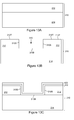
FIG. 13A shows a structure in accordance with an embodiment of the present invention;
FIG. 13B shows a structure in accordance with an embodiment of the present invention;
FIG. 13C shows a structure in accordance with an embodiment of the present invention;
FIG. 14 shows a structure in accordance with an embodiment of the present invention;
FIG. 15 shows a structure in accordance with an embodiment of the present invention;
FIG. 16 shows a structure in accordance with an embodiment of the present invention;
FIGS. 17 through 23 show a method of forming a structure in accordance with an embodiment of the present invention;
FIG. 24 shows a structure in accordance with an embodiment of the present invention; and
FIG. 25 shows a structure in accordance with an embodiment of the present invention.
DETAILED DESCRIPTION OF THE INVENTION
The following detailed description refers to the accompanying drawings that show, by way of illustration, specific details and embodiments in which the invention may be practiced. These embodiments are described in sufficient detail to enable those skilled in the art to practice the invention. Other embodiments may be utilized and structural, logical, and electrical changes may be made without departing from the scope of the invention. The various embodiments are not necessarily mutually exclusive, as some embodiments can be combined with one or more other embodiments to form new embodiments.
FIG. 1 shows a workpiece 210 which may be part of an electronic device such as a semiconductor device. The workpiece 210 may be a homogeneous layer (for example, a dielectric layer). The workpiece 210 may correspond to a semiconductor substrate. The workpiece 210 may include a plurality (e.g. a stack) of sub-layers of different materials (as shown, for example, in FIG. 13A).
The workpiece 210 includes a top surface 210T. An opening 310 may be formed in the workpiece 210 shown in FIG. 1 so as to form the workpiece 210 shown in FIG. 2 that includes an opening 310. The opening 310 may include a bottom surface as well as one or more sidewall surfaces 310S. The opening 310 may have any lateral cross sectional shape. The opening 310 may, for example, be a trench or a hole. In one or more embodiments, workpiece 210 may be or may comprise a dielectric layer such that the opening 310 is formed within a dielectric layer.
Referring to FIG. 2, the opening 310 includes a bottom surface 310B. The opening 310 further includes one or more sidewall surfaces 310S. In one or more embodiments, the sidewall surfaces 310S may be substantially vertical. In other embodiments, the sidewall surface may be tilted or even step-shaped.
Referring to FIG. 3, a barrier layer 410 may be formed over the workpiece 210 (from FIG. 2). In particular, the barrier layer 410 may be formed over the top surface 210T as well as over the sidewall surfaces 310S and bottom surface 310B of the opening 310.
In one or more embodiments, the barrier layer 410 may be formed directly on the workpiece 210 (from FIG. 2) so that the barrier layer may be deposited directly on the top surface 210T as well as directly on the sidewall surfaces 310S and bottom surface 310B of opening 310B. The formation of the barrier layer 410 may be a deposition process such as a substantially conformal deposition. Referring to FIG. 3, the barrier layer 410 may include a top surface 410T, one or more sidewall surfaces 410S and a bottom surface 410B.
The barrier layer 410 may be a conductive layer. In one or more embodiments, the barrier layer 410 may be a metallic layer. The barrier layer may comprise one or more conductive materials. The barrier layer may comprise one or more metallic materials. The barrier layer 410 may comprise, for example, a metal and/or a metallic alloy and/or a compound (e.g. a metallic compound).
In one or more embodiments, a metallic alloy may comprise at least two metallic elements. In one or more embodiments, a metallic alloy may comprise at least one metallic element and at least one non-metallic element (for example, steel).
In one or more embodiments, a metallic alloy may be a binary alloy. In one or more embodiments, a metallic alloy may be a ternary alloy. In one or more embodiments, a metallic alloy may comprise more than three elements.
In one or more embodiments, the barrier layer 410 may be a homogeneous layer. In one or more embodiments, the barrier layer 410 may comprise a combination or mixture of two or more materials. In one or more embodiments, the barrier layer 410 may comprise a stack of two or more sub-layers of different materials.
In one or more embodiments, the barrier layer 410 may comprise at least one of the periodic table chemical elements selected from the group consisting of Ti (titanium), Ta (tantalum), W (tungsten), and N (nitrogen). The chemical elements may be in any form, such as, for example, metals and/or metallic alloys and/or compounds (e.g. metallic compounds).
As an example, the barrier layer may comprise the chemical element Ti (titanium). The Ti may be in any form, such as, a metal (e.g. titanium metal) and/or a metallic alloy (e.g. titanium alloy) and/or a compound (e.g. a metallic compound such as titanium compound). The titanium compound may be titanium nitride (e.g. TiN). In one or more embodiments, the barrier layer may comprise (or may consist essentially of) titanium metal.
In one or more embodiments, the barrier layer may comprise (or may consist essentially of) any Ti-containing material. A Ti-containing material may be any material that includes the chemical element Ti (titanium). In one or more embodiments, this may include any materials that include titanium atoms. The Ti-containing material may be a conductive material. The Ti-containing material may be a metallic material. The Ti-containing material may be a homogeneous material.
Ti-containing materials may include, for example, titanium metal and/or metallic alloys (e.g. titanium alloys) and/or titanium compounds (e.g. metallic titanium compounds). An example of a titanium compound is titanium nitride. In one or more embodiments, the Ti-containing material is titanium metal.
In one or more embodiments, the barrier layer 410 may comprise the chemical element Ta (tantalum). The Ta (tantalum) may be in the form of tantalum metal and/or a metallic alloy (e.g. tantalum alloy) and/or a compound (e.g. a metallic compound) such as tantalum nitride. Likewise, the W (tungsten) may be in the form, for example, of tungsten metal and/or a metallic alloy (such as tungsten alloy) and/or a compound (e.g. a metallic compound) such as tungsten nitride.
In one or more embodiments, the barrier layer may, for example, comprise (or may consist essentially of) one or more materials selected from the group consisting of titanium metal, titanium alloy, titanium compound (e.g. titanium nitride), tantalum metal, tantalum alloy, tantalum compound (e.g. tantalum nitride), tungsten metal, tungsten alloy, tungsten compound (e.g. tungsten nitride). The barrier layer may include mixtures and combinations of materials. In one or more embodiments, the barrier layer may comprise titanium metal. In one or more embodiments, the barrier layer may comprise (or may consist essentially of) titanium-tungsten alloy.
In one or more embodiments, the barrier layer 410 may be a homogeneous layer. For example, in one or more embodiments, the barrier layer 410 may consist essentially of titanium metal. In one or more embodiments, the barrier layer 410 may include a mixture or combination of two or more materials. In one or more embodiments, the barrier layer 410 may comprise a stack of two or more sub-layers. Two or more of the sub-layer may comprise different materials (for example, materials having different compositions). As an example, in one or more embodiments, the barrier layer may comprise a stack of titanium metal/titanium nitride.
The barrier layer 410 may, for example, be deposited using a sputtering process and/or a chemical vapor deposition process.
In one or more embodiments, the barrier layer 410 may have a thickness between about 10 nm and about 100 nm. In one or more embodiments, the barrier layer 410 may have a thickness of about 15 nm or greater. In one or more embodiments the barrier layer 410 may have a thickness of about 50 nm or less. In one or more embodiments the barrier layer 410 may have a thickness of about 30 nm or less. In one or more embodiments, the barrier layer 410 may have a thickness of about 20 nm.
Referring to FIG. 4, a seed layer 420 may then be deposited over the barrier layer 410. The seed layer 420 may be deposited over the top surface 410T of the barrier layer 410 as well as over the sidewall surfaces 410S and the bottom surface 410B of the barrier layer 410. The seed layer 420 may be deposited within the opening 310 as well as outside the opening 310. The deposition of the seed layer may be a substantially conformal deposition. The seed layer 420 may include a top surface 420T, one or more sidewall surfaces 420S and a bottom surface 420B as shown in FIG. 4.
The seed layer 420 may be a conductive layer. The seed layer may be a metallic layer. The seed layer 420 may comprise one or more conductive materials. The seed layer 420 may comprise one or more metallic materials. The seed layer 420 may include a metal and/or a metallic alloy and/or a compound (e.g. a metallic compound). In one or more embodiments, the seed layer may be a homogeneous layer. In one or more embodiments, the seed layer may comprise a combination or mixture of two or more different materials. In one or more embodiments, the seed layer 420 may comprise a stack of two or more sub-layers of different materials.
In one or more embodiments, the seed layer 420 may comprise the chemical element Cu (copper). The Cu may be in any form such as copper metal, metallic alloy (e.g. copper alloy) and/or metallic compound (e.g. copper compound). In one or more embodiments, the copper alloy may include a doped copper.
In one or more embodiments, the seed layer 420 may comprise (or may consist essentially of) the element Cu (copper) and at least one additional element from the periodic table. In one or more embodiments, an additional element may be a metallic element from the period table. In one or more embodiments, an additional element may be a non-metallic element. In one or more embodiments, an additional element may be selected from the group consisting of Al (aluminum), Mn (manganese), Mg (magnesium), V (vanadium), Cr (chromium), Sn (tin), Zn (zinc), and Ti (titanium). In one or more embodiments, the seed layer 420 may comprise atoms of at least one of aluminum atoms, manganese atoms, magnesium atoms, vanadium atoms, chromium atoms, tin atoms, zinc atoms and titanium atoms. In one or more embodiments, the additional element may be Al (aluminum).
Any of the additional elements may be in the form, for example, of a metal and/or metal alloy and/or compound (e.g. metallic compound). As examples, it is possible that that seed layer may include at least one of copper metal, copper alloy, copper compound, manganese metal, manganese alloy, manganese compound, magnesium metal, magnesium alloy, magnesium compound, vanadium metal, vanadium alloy, vanadium compound, chromium metal, chromium alloy, chromium compound, tin metal, tin alloy, tin compound, zinc metal, zinc alloy, zinc compound, titanium metal, titanium alloy, and titanium compound.
The seed layer may include combinations of materials. The seed layer 420 may include an atomic percentage of the element Cu (copper) and an atomic percentage of an addition element (for example, an atomic percentage of the chemical element Al (aluminum) if Al is an additional element). In one or more embodiments, the atomic percentage of the Cu may be about 90% or more, about 95% or more, about 97% or more, about 98% or more, about 99% or more, about 99.5% or more, or about 99.9% or more. In some embodiments, the atomic percent of the Cu may be about 99.9% or less. In one or more embodiments, the atomic percentage of an additional element (for example, Al) may be about 10% or less, 5% or less, 3% or less, 2.5% or less, 2% or less, 1% or less, 0.5% or less, 0.2% or less, or 0.1% or less. In one or more embodiments, the atomic percentage of an additional element may be about 0.1% or more.
In one or more embodiments, there may be more than one additional element. In one or more embodiments, the atomic percentage of all additional elements together (if there is more than one additional element) may be about 10% or less, 5% or less, 3% or less, 2.5% or less, 2% or less, 1% or less, 0.5% or less, 0.2% or less, or 0.1% or less. In one or more embodiments, the atomic percentage of all additional elements together may be about 0.1% or more.
In some embodiments, an additional element may be the chemical element Al (aluminum). Hence, in one or more embodiments, the seed layer may comprise (or may consist essentially of) the element Cu and the element Al. Hence, the seed layer may include both copper atoms and aluminum atoms. The Cu and Al may be in any form such metals (e.g. copper metal and/or aluminum metal), metallic alloy and/or compounds (e.g. metallic compounds). In one or more embodiments, seed layer may comprise a metallic alloy that comprises (or consists essentially of) the elements Cu and Al. In one or more embodiments, the metallic alloy may be a copper alloy. In one or more embodiments, the copper alloy may be a copper-aluminum alloy. In one or more embodiments, the copper-aluminum alloy may be an aluminum-doped copper.
In some embodiments, the seed layer may comprise (or may consist essentially of) a material (e.g. a seed layer material) that includes Cu (copper) and the one or more additional chemical elements as described above. In one or more embodiments, an additional element may be Al (aluminum). In some embodiments, the seed layer material may be a homogenous material. In some embodiments, the seed layer material may be a metallic material. In some embodiments, the seed layer material may include at least one metal and/or at least one metallic alloy and/or at least one compound (e.g. metallic compound).
As noted, an additional element may be Al (aluminum). Hence, the seed layer material may include Cu (copper) and (Al) aluminum. This material may be referred to as a Cu/Al-containing material. Hence, the Cu/Al-containing material may be any material that includes Cu (copper) and Al (aluminum). For example, the Cu/Al-containing material may include copper atoms and aluminum atoms. In one or more embodiments, the Cu/Al material may consist essentially of the elements Cu (copper) and Al (aluminum). The Cu/Al-containing material may be a conductive material. The Cu/Al-containing material may be a metallic material. In one or more embodiments, the Cu/Al material may be a homogeneous material.
The seed layer material may include an atomic percentage of the element Cu (copper) and an atomic percentage of an addition element (for example, the chemical element Al (aluminum)). In one or more embodiments, the atomic percentage of the Cu may be about 90% or more, about 95% or more, about 97% or more, about 98% or more, about 99% or more, about 99.5% or more, or about 99.9% or more. In some embodiments, the atomic percent of the Cu may be about 99.9% or less. In one or more embodiments, the atomic percent of an additional element (for example, Al) may be about 10% or less, 5% or less, 3% or less, 2.5% or less, 2% or less, 1% or less, 0.5% or less, 0.2% or less, or 0.1% or less. In one or more embodiments, the atomic percentage of an additional element may be about 0.1% or more.
In one or more embodiments, the atomic percent of all additional elements together (if there is more than one additional element) may be about 10% or less, 5% or less, 3% or less, 2.5% or less, 2% or less, 1% or less, 0.5% or less, 0.2% or less, or 0.1% or less. In one or more embodiments, the atomic percentage of all additional elements together may be about 0.1% or more.
In some embodiments, the seed layer material may include a metallic alloy. Hence, in one or more embodiments, the seed layer 420 may comprise (or may consist essentially of) a metallic alloy. The metallic alloy may comprise (or may consist essentially of) the chemical element Cu and at least one additional element. As discussed, in one or more embodiments, an additional element may be a metallic element. In one or more embodiments, an additional element may be a non-metallic element. In one or more embodiments, an additional element may be selected from the group consisting of Al (aluminum), Mn (manganese), Mg (magnesium), V (vanadium), Cr (chromium), Sn (tin), Zn (zinc), and Ti (titanium).
Hence, in one or more embodiments, the seed layer 420 may comprise a metallic alloy. The metallic alloy may include an atomic percentage of the element Cu (copper) and an atomic percentage of an additional element (for example, the chemical element Al (aluminum)). In one or more embodiments, the atomic percentage of the Cu may be greater than about 50%, about 90% or more, about 95% or more, about 97% or more, about 98% or more, about 99% or more, about 99.5% or more, or about 99.9% or more. In some embodiments, the atomic percent of the Cu may be about 99.9% or less. In one or more embodiments, the atomic percent of an additional element (for example, Al) may be about 10% or less, 5% or less, 3% or less, 2.5% or less, 2% or less, 1% or less, 0.5% or less, 0.2% or less, or 0.1% or less. In one or more embodiments, the atomic percentage of an additional element may be about 0.1% or more.
In one or more embodiments, the atomic percent of all additional elements together (if there is more than one additional element) may be about 10% or less, 5% or less, 3% or less, 2.5% or less, 2% or less, 1% or less, 0.5% or less, 0.2% or less, or 0.1% or less. In one or more embodiments, the atomic percentage of all additional elements together may be about 0.1% or more.
In one or more embodiments, the metallic alloy may comprise (or may consist essentially of) Cu (copper) and Al (aluminum). The metallic alloy may be a copper alloy such as a copper-aluminum alloy.
The seed layer 420 may be deposited using a sputtering process and/or a chemical vapor deposition process and/or a physical vapor deposition.
In one or more embodiments, the seed layer 420 may have a thickness between about 25 nm (nanometer) and about 150 nm. In one or more embodiments, the seed layer 420 may have a thickness of about 30 nm (nanometer) or greater. In one or more embodiments, the seed layer 420 may have a thickness of about 35 nm (nanometer) or greater. In one or more embodiments, the seed layer 420 may have a thickness of about 40 nm (nanometer) or greater. In one or more embodiments, the seed layer 420 may have a thickness of about 100 nm (nanometer) or less. In one or more embodiments, the seed layer 420 may have a thickness may be about 75 nm or less. In one or more embodiments, the seed layer 420 may have a thickness may be about 50 nm.
Referring to FIG. 5, a masking layer 510 may then be deposited over the seed layer 420. In one or more embodiments, the masking layer 510 may be a photoresist layer. The masking layer 410 may be deposited over the top surface 420T, the sidewall surfaces 420S and the bottom surface 420B of the seed layer 420. The masking layer 510 may be deposited within the opening 310 as well as outside the opening 310. In one or more embodiments, the masking layer 510 may comprise a galvanic resist material.
Referring to FIG. 6, a portion of the masking layer 510 may be removed so as to form an opening 610 within the masking layer 510. In one or more embodiments, the removal of the masking layer 510 may comprise a selective removal process. The masking layer 510 may be removed from within the opening 310. The opening 610 may viewed as including an upper portion 610B and a lower portion 610A.
Referring to FIG. 7, a fill layer 710 may be deposited within the opening 610. The fill layer 710 may be formed over the seed layer 420. The deposition may comprise an electroplating process. The electroplating process may utilize an electrodeposition process. The fill layer 710 may be electroplated over (for example, directly on) the seed layer. After the deposition of the fill layer 710, a chemical mechanical polishing process may be applied to create a level top surface as shown in FIG. 7.
The fill layer 710 may be a conductive layer. The fill layer 710 may be a metallic layer. The fill layer 710 may comprise at least one metallic material. The metallic material may, for example, be in the form of a metal, a metallic alloy or metallic compound. In one or more embodiments, the fill layer may comprise a homogeneous layer.
In one or more embodiments, the fill layer 710 may comprise at least one of the periodic table chemical elements selected from the group consisting of the elements Cu (copper), Al (aluminum), Au (gold), and Ag (silver). Each of the periodic table chemical elements may, for example, be in any form such as a metal and/or a metallic alloy and, even, possibly a metallic compound. For example, the Cu (copper) may, for example, be in the form of copper metal and/or a metallic alloy (for example, a copper alloy) and/or a metallic compound (for example, a metallic copper compound). The same is true for the other chemical elements.
Referring to FIG. 8, the masking layer 510 (for example, a photoresist layer) may be removed. The removal may be accomplished by an etching process. The etching process may comprise a wet etching process. The etching process may comprise a dry etching process.
Referring to FIG. 9, a barrier layer 810 may be deposited over the fill layer 710 as well as over the top surface of the seed layer 420. In one or more embodiments, the barrier layer 810 may include one or more of the materials as described above with regards to barrier layer 410. In one or more embodiments, the barrier layer 810 may include the same materials as barrier layer 410. In one or more embodiments, the barrier layer 810 may include one or more different materials from barrier layer 410.
Referring to FIG. 10, a dielectric layer 910 may be formed over the barrier layer 810 (and over the fill layer 710). The dielectric layer 910 may comprise one or more dielectric materials. The dielectric materials may be selected from the group consisting of oxide, nitride, oxynitride, and combinations thereof. The dielectric layer may comprise a combination (e.g. mixture) of two or more materials.
Referring to FIG. 11, an opening 950 may be formed through the dielectric layer 910 and the barrier layer 810 so as to expose a top surface 710T of the fill layer 710.
Referring to FIG. 12, at least one anneal process may be performed. The anneal process may cause materials from seed layer 420 as well as from the barrier layer 410 to move (e.g. migrate) into the fill layer 710. The movement may be the result of a diffusion process. More particularly, the anneal process may cause these materials to move through the fill layer 710 to the exposed top surface 710T of the fill layer 710.
As discussed, the seed layer may include the chemical element Al (aluminum) (and/or possibly some other additional element(s)). Also, the barrier layer may include the chemical element Ti (titanium). As a result of the anneal process, the Al (aluminum) from the seed layer 420 (and/or possibly some other additional element(s) from the seed layer) may move into the fill layer 710 and move to the top surface 710T of the fill layer 710. Likewise, Ti (titanium) from the barrier layer 410 may move into the fill layer 710 and move to the top surface 710T of the fill layer 710.
It is noted that the movement of the Ti (titanium) may be in the form of titanium atoms. Likewise, the movement of the Al (aluminum) from the seed layer may be in the form of atoms (e.g. aluminum atoms). The titanium atoms and/or aluminum atoms may be individual atoms or they may be part of more complex structures such as molecules and/or compounds. Individual atoms may be neutral atoms or may be ions.
While not wishing to be bound by theory, the movement of the Ti (titanium) and Al (aluminum) may be by a diffusion mechanism.
The Ti (titanium) and/or Al (aluminum) may reach the top surface 710T. Referring to FIG. 12, a passivation layer 1010 may form over at least a portion of the exposed top surface 710T of fill layer 710. The passivation layer 1010 may include the Ti (titanium) and/or the Al (aluminum) that has come from the barrier layer and/or the seed layer. Hence, in one or more embodiments, it may not be necessary to deposit the Ti and/or the Al over the top of the fill layer.
Hence, in one or more embodiments, the passivation layer 1010 may form from self passivation process in that at least a portion of the components (e.g. chemical elements) of the passivation layer may come from the structure itself. For example, at least a portion of the components (e.g. chemical elements) of the passivation layer may come from the fill layer and/or the seed layer and/or the barrier layer and/or the workpiece. In one or more embodiments, at least a portion of the components (e.g. chemical elements) of the passivation layer may come from the barrier layer and/or the seed layer.
In one or more embodiments, the passivation layer 1010 may include both Ti (titanium) and Al (aluminum). In one or more embodiments, the passivation layer 1010 may include the periodic table chemical element O (oxygen) and/or the period table chemical element N (nitrogen). In one or more embodiments, the passivation layer 1010 may be a homogeneous layer. In one or more embodiments, the passivation layer 1010 may include two or more sub-layers of different materials. In one or more embodiments, the passivation layer may be a conductive layer. In one or more embodiments, the passivation layer may be a metallic layer. In one or more embodiments, the passivation layer may be a dielectric layer. In one or more embodiments, the dielectric layer may include one or more oxides.
In one or more embodiments, the passivation layer 1010 may include a material that includes Ti (titanium) and/or Al (aluminum). The material may, for example, include one or more metals, one or more metallic alloys and/or one or more compounds. The one or more compounds may include one or more metallic compounds and/or one or more non-metallic compounds.
The passivation layer may include one or more non-metallic compounds. The passivation layer may include one or more dielectric materials. The passivation layer may include at least one oxide and/or at least one nitride.
In one or more embodiments, the passivation layer 1010 may comprise a compound that includes (1) periodic table chemical element O (oxygen) and/or the periodic table element N (nitrogen) and (2) at least one of the periodic table chemical elements Al (aluminum) and Ti (titanium). In one or more embodiments, the passivation layer 1010 may comprise a compound that includes (1) periodic table chemical element O (oxygen) and/or N and (2) both Al (aluminum) and Ti (titanium). In one or more embodiments, the compound may be a non-metallic compound. In one or more embodiments the compound may be a metallic compound. In one or more embodiments, the compound may be a dielectric material. In one or more embodiments, the compound may be an oxide. In one or more embodiments, the compound may be a nitride.
In one or more embodiments, the passivation layer may include an oxide that includes at least one of Al (aluminum) and Ti (titanium). In one or more embodiments, the passivation layer may comprise an oxide that includes O (oxygen) and both Al (aluminum) and Ti (titanium). In one or more embodiments, the passivation layer may include an oxide that includes both Al (aluminum) and Ti (titanium). In one or more embodiments, the passivation layer may include aluminum oxide (for example, Al203) and/or titanium oxide (for example, Ti02).
In one or more embodiments, the Al (aluminum) of the passivation layer 1010 may be in the form of a compound. In one or more embodiments, the Al (aluminum) of the passivation layer 1010 may be in the form of aluminum oxide (for example, Al2O3). In one or more embodiments, the Ti (titanium) of the passivation layer 1010 may be in the form of a compound. In one or more embodiments, the Ti (titanium) of the passivation layer 1010 may be in the form of titanium oxide (for example, TiO2). In one or more embodiments, the passivation layer 1010 may include aluminum oxide and/or titanium oxide. In one or more embodiments, the passivation layer 1010 may include both aluminum oxide and titanium oxide.
The passivation layer 1010 may serve to increase the corrosion resistance of the surface of the fill layer 710 for such activities as probing and wire bonding. For example, the protective layer 1010 may help to inhibit or eliminate the growth of other oxides (such as copper oxide) on the top surface 710T of the fill layer 710. The passivation layer 1010 may thus serve as a passivation layer which may help to reduce or prevent the formation of unwanted materials (e.g. for example, oxides such as copper oxide) on the top surface of the fill layer.
In one or more embodiments, the passivation layer 1010 may be in direct contact with the top surface 710T of the fill layer 710.
Referring once again to FIG. 12, it is noted that the elements Ti (titanium) and Al (aluminum) are shown in FIG. 12 as moving to a top surface of the fill layer 710. It is noted that instead of Al (or in addition to Al) it is, of course, possible that at least one other additional element (as discussed above) moves from the seed layer 420 to the top surface of the fill layer 710. Hence, the passivation layer may include any of the additional elements added to the seed layer. As noted, in some embodiments, an additional element may a metallic element. In some embodiments, an additional element may be a non-metallic element. In some embodiments, an additional element may be selected from the group consisting of Al, Mg, Mn, V, Cr, Sn, and Zn. The additional elements may thus appear in the passivation layer.
In some embodiments, the chemical element Ti may be added to the seed layer. Hence, in some embodiments, it may be possible that the Ti as well as the Al (and/or at least one other additional element) may come from the seed layer and move to a top surface of the fill layer as a result of the anneal process. The Ti as well as one or more of the additional element may appear in the passivation layer.
In some embodiments, it may also be possible that a first element from the barrier layer and/or the seed layer as well as a second element from the barrier layer/or the seed layer move to a top surface of the fill layer as a result of the anneal process. The first element and the second element may appear in the passivation layer.
It is possible that during wire bonding and/or probing at least a portion of the passivation layer 1010 may be removed. It is possible, in one or more embodiments, that at least a portion of the passivation layer remains. Hence, in one or more embodiments, the passivation layer may overlie at least a portion of the top surface 710T of the fill layer 710.
In one or more embodiments, the anneal process may take place at a temperature which is equal to or greater than about 100° C. In one or more embodiments, the anneal process may take place at a temperature which is equal to or greater than about 250° C. In one or more embodiments, the anneal process may take place at a temperature which is equal to or greater than about 300° C. In one or more embodiments, the anneal process may take place at a temperature which is equal to or greater than about 350° C. In one or more embodiments, the anneal process may take place at a temperature which is equal to or greater than about 400° C. In one or more embodiments, the anneal process may take place at a temperature which is equal to or greater than about 450° C. In one or more embodiments, the anneal process may take place at a temperature which is equal to or less than about 550° C. In one or more embodiments, the anneal process may take place at a temperature which is less than or equal to about 500° C.
In one or more embodiments, the anneal process may have a time period of about 5 minutes or greater. In one or more embodiments, the anneal process may have a time period of about 10 minutes or greater. In one or more embodiments, the anneal process may have a time period of about 15 minutes or greater. In one or more embodiments, the anneal process may have a time period of about 30 minutes or greater. In one or more embodiments, the anneal process may have a time period of about 45 minutes or greater. In one or more embodiments, the anneal process may have a time period of about 60 minutes or greater. In one or more embodiments, the anneal process may have a time period of about 75 minutes or greater. In one or more embodiments, the anneal process may have a time period of about 90 minutes or less.
In some embodiments, it is conceivable that any of the temperatures provided above may be used in combination with any of the time periods provided above to provide anneal processes having temperatures and time periods.
Referring again to FIG. 11, in one or more embodiments, the fill layer 710 may have a thickness TH of at least about 1.5 microns (μm). In one or more embodiments, the fill layer 710 may have a thickness of at least about 2 microns. In one or more embodiments, the fill layer 710 may have a thickness of at least about 2.5 microns. In one or more embodiments, the fill layer 710 may have a thickness of at least about 3 microns. In one or more embodiments, the fill layer 710 may have a thickness of at least about 3.5 microns. In one or more embodiments, the fill layer 710 may have a thickness of at least about 4 microns. In one or more embodiments, the fill layer 710 may have a thickness of at least about 4.5 microns. In one or more embodiments, the fill layer 710 may have a thickness of at least about 5 microns. In one or more embodiments, the fill layer 710 may have a thickness of at least about 5.5 microns. In one or more embodiments, the fill layer 710 may have a thickness of at least about 6 microns. In one or more embodiments, the fill layer 710 may have a thickness of about 7 microns or less.
In one or more embodiments, portion 710B of fill layer 710 may have a thickness of at least about 0.5 microns (μm). In one or more embodiments, the portion 710B of fill layer 710 may have a thickness of at least about 1 microns. In one or more embodiments, the portion 710B of fill layer 710 may have a thickness of at least about 1.5 microns. In one or more embodiments, the portion 710B of fill layer 710 may have a thickness of at least about 2 microns. In one or more embodiments, the portion 710B of fill layer 710 may have a thickness of at least about 2.5 microns. In one or more embodiments, the portion 710B of fill layer 710 may have a thickness of at least about 3 microns. In one or more embodiments, the portion 710B of fill layer 710 may have a thickness of at least about 3.5 microns. In one or more embodiments, the portion 710B of fill layer 710 may have a thickness of at least about 4 microns. In one or more embodiments, the portion 710B of fill layer 710 may have a thickness of at least about 4.5 microns. In one or more embodiments, the portion 710B of fill layer 710 may have a thickness of at least about 5 microns.
Referring again to FIG. 1, it is understood that, one or more embodiments, the workpiece 210 may, for example, represent a layer, such as a dielectric layer so that the workpiece 210 shown in FIG. 2 may represent a dielectric layer having an opening 310. Likewise, it may be possible that the workpiece 210 from FIG. 1 represent a substrate (e.g. a semiconductor substrate) such that the workpiece 210 shown in FIG. 2 may represent a substrate having an opening.
However, it may also be possible that the workpiece 210 from FIG. 1 represent a combination (for example, a stack) of two or more layers. Likewise, the workpiece 210 from FIG. 2 may represent a combination (for example, a stack) of two or more layers having an opening 310.
FIG. 13A shows that workpiece 210 may represent a layer 212 over a layer 214. Referring to FIG. 13B, the opening 310 may thus be formed within (or through) the layer 212. The opening may, for example, expose the layer 214. The layer 212 may have a top surface 212T corresponding to the top surface of the workpiece 210. FIG. 13C shows (as is shown in FIG. 4) that the barrier layer 410 may be formed over the workpiece 210 that includes opening 310. This time, the workpiece 210 includes a layer 212 over a layer 214, so that the opening 310 is formed within (or through) the layer 212. It may be possible that the barrier layer 410 is makes direct contact the layer 214.
FIG. 14 shows the same structure from FIG. 12, except that the workpiece 210 is now shown to include a layer 212 over a layer 214. In one or more embodiments, the layer 212 may be dielectric layer. The layer 212 may include one or more dielectric materials such as an oxide (such as silicon oxide), a nitride (such as silicon nitride) and/or an oxinitride (such as silicon oxinitride). In one or more embodiments, the layer 212 may be passivation layer for a semiconductor chip or integrated circuit.
Referring to FIG. 14, in one or more embodiments, layer 214 may include (or may be) a substrate. A substrate may be any substrate such as a semiconductor substrate. The semiconductor substrate may be a bulk-semiconductor substrate (such as a bulk-silicon substrate). The semiconductor substrate may be an SOI substrate (e.g. a semiconductor on insulator substrate). The SOI substrate may be a silicon on insulator substrate.
In some embodiments, the portion 710B (as seen in FIG. 14) may represent a metal line of a metallization level. Likewise, in some embodiments, the portion 710A may represent a conductive via that electrical couples the portion 710B (for example, a metal line) to the substrate 214. A conductive via that coupled a metallization level to a semiconductor substrate may also be referred to as a conductive contact.
Referring to FIG. 15, the layer 214 may include two or more layers (e.g. a stack of layers). For example, the layer 214 may include (or may consist essentially of) a layer dielectric layer 218 overlying a layer 220. A metal line 216 is embedded within the dielectric layer 218. The dielectric layer 218 may represent an inter-level dielectric layer and the metal line may represent the metal line of a metallization level. The metallization level may, for example, be metal-1 so that layer 220 may represent a substrate (e.g. a semiconductor substrate). However, the metallization level of metal line 216 may present a level above metal-1. In such as case, as shown in FIG. 16, the layer 220 may include a layer 222 overlying a layer 224. In such a case, the layer 222 may represent additional metallization levels and inter-level dielectric layers while the layer 220 may include (or may be) a substrate (such as a semiconductor substrate). In one or more embodiments, the metal line 216 may represent a final metal line of a final metallization level. In this case, the portion 710B may still represent a metal line. Likewise, the portion 710A may still represent a conductive via. It is understood that a metal line may include a metal pad.
As noted, the layer 222 may include one or more metallization levels. The metal line 216 may be part of a metallization level of the semiconductor chip. In one or more embodiments, the portion 710A may represent a conductive via which electrically couples the metal line 710B (belonging to an upper metallization level to the metal line 216 (belonging to a lower metallization level). It is noted that a metal line may itself include a pad structure (e.g. a bonding pad, a contact pad and/or a landing pad).
It is noted that in some embodiments, a metal line may be particularly useful in routing electrical signals primarily in a horizontal direction. It is further noted that in some embodiments, a conductive via may be particularly useful in routing electrical signals primarily in a vertical direction.
Still referring to FIG. 16, in some embodiments, the metal line 216 may be a final metal line belonging to a final or top metallization level. The dielectric layer 212 may, in some embodiments, represent a passivation layer for a semiconductor chip or integrated circuit. The fill layer 710 may represent a bond pad. The bond pad 710 may be disposed above the final metallization level and may overlie the final metal line 216 of a final metallization level of a semiconductor chip and/or integrated circuit. A bond pad 710 may include a lower portion 710A of the fill layer 710 formed through the passivation layer 212 and an upper portion 710B of fill layer 710 formed over the portion 710A so as to provide additional strength and reinforcement. The bond pad 710 may be used for wiring bonding or for probing purposes.
Hence, a wire bond may be electrically coupled to the bond pad 710 through the opening 950. The passivation layer 1010 may help to protect the bond pad 950 from the formation of unwanted oxides. For example, when the bond pad 710 comprises copper metal and/or a copper alloy, the passivation layer 1010 may help to prevent the formation of unwanted copper oxide.
As noted, the metal line 216 may itself include a pad structure. The pad structure may be a relatively wider portion than a remaining portion of the metal line. The bond pad portion of metal line 220 may underlie the bond pad 710.
Referring once again, to FIG. 2, in the embodiment shown, it is seen that, in one or more embodiments, an opening 310 may be formed in the workpiece 210 prior to the formation of the barrier layer 410 or the seed layer 420. However, in one or more embodiments, the opening 310 need not be formed. This is illustration in the process shown in FIGS. 17 through 21.
FIG. 17 shows a workpiece 1210. The workpiece 1210 may be any workpiece. It is understood that, in some embodiments, the workpiece 1210 may not be the same as workpiece 210 shown in FIG. 1. In one or more embodiments, the workpiece 1210 may, for example, correspond to the layer 214 shown in FIG. 2B. In one or more embodiments, the workpiece 1210 may, for example, correspond to the workpiece 210 shown in FIG. 1. In some embodiments, the workpiece 1210 may have a substantially planar top surface 1210T. The workpiece 1210 may be a single homogeneous layer or in may include a plurality of layers. The workpiece 1210 may include conductive, semiconductive and/or dielectric materials.
A barrier layer 410 (as described above) may be formed over the workpiece 1210. A seed layer 420 (as described above) may be formed over the barrier layer 410. A masking layer 510 may be formed over the seed layer 420. In one or more embodiments, the masking layer 510 may be a photoresist layer.
Referring to FIG. 18, an opening 610 may formed through the masking layer 510 so as to expose the seed layer 420. Referring to FIG. 19, a fill layer 710 may be formed over the seed layer within the opening 610. The fill layer 710 may be formed by an electroplating process onto the seed layer 420.
Referring to FIG. 20, the masking layer 510 is removed. Referring to FIG. 21, a second barrier layer 810 may be formed over the fill layer 710. A dielectric layer 910 may be formed over the barrier layer 810.
Referring to FIG. 22 an opening 950 is formed through the dielectric layer 910 and through the barrier layer 810 so as to expose the fill layer 710. FIG. 21 shows the formation of the passivation layer 1010 after the anneal process, as explained above.
Referring again to FIG. 22, in one or more embodiments, the fill layer 710 may have a thickness TH of at least about 2 microns (W. In one or more embodiments, the fill layer 710 may have a thickness of at least about 2.5 microns. In one or more embodiments, the fill layer 710 may have a thickness of at least about 3 microns. In one or more embodiments, the fill layer 710 may have a thickness of at least about 3.5 microns. In one or more embodiments, the fill layer 710 may have a thickness of at least about 4 microns. In one or more embodiments, the fill layer 710 may have a thickness of at least about 4.5 microns. In one or more embodiments, the fill layer 710 may have a thickness of at least about 5 microns.
Referring to FIG. 23, a passivation layer 1010 (as explained above) may be formed. As explained above, the passivation layer 1010 may be formed as a result of an anneal process. The anneal process may cause the diffusion of Ti (titanium) and/or Al (aluminum) (or other additional elements as described above) to the top surface of the fill layer 710.
Referring to FIG. 23, the layer 710 may also represent a bonding pad or some other conductive feature such as a metal line, conductive via, etc. The semiconductor structure show in FIG. 23 may represent a semiconductor device and/or a semiconductor chip and/or an integrated circuit.
Referring to FIG. 23, it is possible that workpiece 1210 represent a substrate (such as a semiconductor conductive). However, it is possible that workpiece 1210 may include a plurality of layers. For example, referring to FIG. 24, workpiece 1210 may include a dielectric layer 218 over a layer 220 where the layer 218 represents an inter-level dielectric layer. In some embodiments, a metal line 216 may be embedded within the dielectric layer 218. The metal line 216 may be part of a metallization level such as metal-1, metal-2, metal-3, all the way to the final or top metallization level.
The layer 220 shown in FIG. 24 may, for example, represent a substrate (e.g. a semiconductor substrate). However, referring to FIG. 25, it is also possible that the layer 220 include a layer 222 over a layer 224. In this case, it is possible that layer 222 represent one or more inter-level dielectric layers as well as one or more metallization levels. In this case, it is possible that layer 224 represent a substrate, such as a semiconductor substrate.
It is noted that the metal line 216 shown in FIGS. 13, 14 and again in FIGS. 24, 25 may comprise a conductive material such as a metallic material. Examples of materials include copper metal, copper alloy, aluminum metal and aluminum alloy. Other materials are also possible.
In some embodiments, the use of a combination of a barrier layer that includes Ti (titanium) (which may be in the form of titanium metal) as well as a seed layer that includes Al (aluminum) (which may, for example, be in the form of a metallic alloy such as a copper-aluminum alloy) may provide synergistic and unexpected results that may bring both Ti (titanium) and aluminum (Al) to the top surface of the fill layer.
While not wishing to be bound by theory, it may be possible that the use of a barrier layer that includes Ti (titanium) (which may, for example, be in the form of tantalum metal), as well as a seed layer that in includes Al (aluminum) (which may, for example, be in the form of a copper-aluminum alloy), may provide a synergistic effect in that that Ti (titanium) may help bring the Al (aluminum) to the top surface of the fill layer and the Al (aluminum) may help bring the Ti (titanium) to the top surface of the fill layer.
As noted above, one or more other additional elements may be used in additional to the Al or instead of the Al.
Illustrative Example
A) Using a 20 nm thick barrier layer of titanium metal, a 100 nm thick seed layer of copper-aluminum alloy (with about 2 atomic percent Al (aluminum)) and a 3 micron thick fill layer of copper metal. Annealing at about 380° C. for about 60 minutes forms both Ti (titanium) and Al (aluminum) to the top surface of the fill layer.
B) Using a 25 nm thick barrier layer of tantalum metal, a 100 nm thick seed layer of copper-aluminum alloy (with about 2 atomic percent Al (aluminum)) and a 3 micron thick copper metal fill layer. Annealing at about 380° C. for about 60 minutes does not bring Al (aluminum) to the top surface of the fill layer.
C) Using a 40 nm thick barrier layer of titanium metal, a 50 nm thick seed layer of copper metal and a 3 micron thick fill layer of copper metal. Annealing at about 380° C. for about 60 minutes does not bring the Ti (titanium) to the top surface of the fill layer.
One or more embodiments relate to a method of forming a semiconductor device, comprising: forming a structure, the structure including at least a first element and a second element; and forming a passivation layer over the structure, the passivation layer including at least the first element and the second element, the first element and the second element of the passivation layer coming from the structure. In one or more embodiments, forming the structure may comprise: providing a workpiece; forming a barrier layer over the workpiece; forming a seed layer over the barrier layer; and forming a fill layer over the seed layer.
One or more embodiments relate to a method of forming a semiconductor structure, comprising: providing a workpiece; forming a barrier layer over the workpiece, the barrier layer including Ti (titanium); forming a seed layer over the barrier layer, the seed layer comprising Cu (copper) and an additional element; and forming a fill layer over the seed layer, the fill layer including Cu (copper).
One or more embodiments relate to a semiconductor structure, comprising: a workpiece; a barrier layer overlying the workpiece, the barrier layer including a first element; a seed layer overlying the barrier layer, the seed layer including a metallic alloy, the metallic alloy including Cu (copper) and a second element; and a fill layer overlying the seed layer, the fill layer comprising Cu (copper).
It is to be understood that the disclosure set forth herein is presented in the form of detailed embodiments described for the purpose of making a full and complete disclosure of the present invention, and that such details are not to be interpreted as limiting the true scope of this invention as set forth and defined in the appended claims.

Claims (22)

What is claimed is:
1. A method of forming a semiconductor device, comprising:
forming a barrier layer over a workpiece, said barrier layer including a first metallic element;
forming a seed layer over said barrier layer, said seed layer including a second metallic element;
forming a fill layer over said seed layer;
and
forming a passivation layer over said fill layer, said passivation layer including at least said first metallic element and said second metallic element.
2. The method of claim 1 wherein said first metallic element and said second metallic element are selected from the group consisting of Al (aluminum), Mg (magnesium), Mn (manganese), V (vanadium), Cr (chromium), Sn (tin), Zn (zinc), and Ti (titanium).
3. The method of claim 1, wherein first metallic element is Ti (titanium) and said second metallic element is Al (aluminum).
4. The method of claim 1, wherein said seed layer and/or said fill layer comprises the element Cu (copper).
5. The method of claim 1, wherein said seed layer comprises a metallic alloy, said alloy includes the element Cu (copper) and said second metallic element.
6. The method of claim 1, wherein said workpiece includes an opening, said barrier layer formed within said opening.
7. The method of claim 1, wherein said first metallic element is Ti (titanium).
8. The method of claim 1, wherein said second metallic element is Al (aluminum).
9. The method of claim 1, wherein said first metallic element is Ti (titanium) and said second metallic element is Al (aluminum).
10. The method of claim 1, wherein the atomic percentage of said second metallic element in said seed layer is more than 0.1%.
11. The method of claim 1, wherein forming said passivation layer comprises an anneal process.
12. A method of forming a semiconductor structure, comprising:
providing a workpiece;
forming a barrier layer over said workpiece, said barrier layer including the element Ti (titanium);
forming a seed layer over said barrier layer, said seed layer comprising the element Cu (copper) and an additional metallic element;
forming a fill layer over said seed layer, said fill layer including the element Cu (copper); and
forming a passivation layer over said fill layer, said passivation layer including said element Ti (titanium) and said additional metallic element.
13. The method of claim 12, wherein said passivation layer includes at least one oxide and/or at least one nitride.
14. The method of claim 12, wherein
said element Ti (titanium) of said barrier layer is in the form of titanium metal and/or a titanium-tungsten alloy.
15. The method of claim 12, wherein said additional metallic element is an element selected from the group consisting of Al (aluminum), Mg (magnesium), Mn (manganese), V (vanadium), Cr (chromium), Sn (tin), and Zn (zinc).
16. The method of claim 15, wherein said additional element is Al (aluminum).
17. The method of claim 12, wherein
said seed layer comprises a metallic alloy, said alloy including said element Cu (copper) and said additional element.
18. The method of claim 17, wherein the atomic percentage of said Cu is at least 95%.
19. The method of claim 12, wherein said workpiece includes an opening, said barrier layer formed within said opening.
20. The method of claim 12, wherein said fill layer comprises copper metal and/or copper alloy.
21. The method of claim 11, wherein said anneal causes the movement of said first metallic element from said barrier layer and said second metallic element from said seed layer to form said passivation layer.
22. The method of claim 12, wherein the atomic percentage of said additional metallic element in said seed layer is more than 0.1%.
US12/892,947 2010-09-29 2010-09-29 Semiconductor structure having metal oxide or nirtride passivation layer on fill layer and method for making same Expired - Fee Related US8872341B2 (en)

Priority Applications (3)

Application Number Priority Date Filing Date Title
US12/892,947 US8872341B2 (en) 2010-09-29 2010-09-29 Semiconductor structure having metal oxide or nirtride passivation layer on fill layer and method for making same
DE102011053107A DE102011053107A1 (en) 2010-09-29 2011-08-30 Semiconductor structure and method for its production
US13/300,692 US9064875B2 (en) 2010-09-29 2011-11-21 Semiconductor structure and method for making same

Applications Claiming Priority (1)

Application Number Priority Date Filing Date Title
US12/892,947 US8872341B2 (en) 2010-09-29 2010-09-29 Semiconductor structure having metal oxide or nirtride passivation layer on fill layer and method for making same

Related Child Applications (1)

Application Number Title Priority Date Filing Date
US13/300,692 Continuation-In-Part US9064875B2 (en) 2010-09-29 2011-11-21 Semiconductor structure and method for making same

Publications (2)

Publication Number Publication Date
US20120074573A1 US20120074573A1 (en) 2012-03-29
US8872341B2 true US8872341B2 (en) 2014-10-28

Family

ID=45804815

Family Applications (1)

Application Number Title Priority Date Filing Date
US12/892,947 Expired - Fee Related US8872341B2 (en) 2010-09-29 2010-09-29 Semiconductor structure having metal oxide or nirtride passivation layer on fill layer and method for making same

Country Status (2)

Country Link
US (1) US8872341B2 (en)
DE (1) DE102011053107A1 (en)

Cited By (2)

* Cited by examiner, † Cited by third party
Publication number Priority date Publication date Assignee Title
US10297562B2 (en) * 2017-03-14 2019-05-21 Ablic Inc. Semiconductor device and method of manufacturing a semiconductor device
US11270963B2 (en) * 2020-01-14 2022-03-08 Sandisk Technologies Llc Bonding pads including interfacial electromigration barrier layers and methods of making the same

Families Citing this family (7)

* Cited by examiner, † Cited by third party
Publication number Priority date Publication date Assignee Title
US8872341B2 (en) * 2010-09-29 2014-10-28 Infineon Technologies Ag Semiconductor structure having metal oxide or nirtride passivation layer on fill layer and method for making same
US9064875B2 (en) 2010-09-29 2015-06-23 Infineon Technologies Ag Semiconductor structure and method for making same
US20130241058A1 (en) * 2012-03-16 2013-09-19 Taiwan Semiconductor Manufacturing Company, Ltd. Wire Bonding Structures for Integrated Circuits
TW201444021A (en) * 2013-05-10 2014-11-16 Univ Nat Cheng Kung Cu/CuMn barrier layer
JP6300533B2 (en) * 2014-01-15 2018-03-28 ルネサスエレクトロニクス株式会社 Semiconductor device manufacturing method and semiconductor device
US9704804B1 (en) 2015-12-18 2017-07-11 Texas Instruments Incorporated Oxidation resistant barrier metal process for semiconductor devices
US10985011B2 (en) * 2017-11-09 2021-04-20 Taiwan Semiconductor Manufacturing Co., Ltd. Structure and formation method of semiconductor device with resistive elements

Citations (29)

* Cited by examiner, † Cited by third party
Publication number Priority date Publication date Assignee Title
US5913147A (en) * 1997-01-21 1999-06-15 Advanced Micro Devices, Inc. Method for fabricating copper-aluminum metallization
US6025275A (en) 1996-12-19 2000-02-15 Texas Instruments Incorporated Method of forming improved thick plated copper interconnect and associated auxiliary metal interconnect
US6153521A (en) 1998-06-04 2000-11-28 Advanced Micro Devices, Inc. Metallized interconnection structure and method of making the same
US6218732B1 (en) 1998-09-15 2001-04-17 Texas Instruments Incorporated Copper bond pad process
US6249055B1 (en) * 1998-02-03 2001-06-19 Advanced Micro Devices, Inc. Self-encapsulated copper metallization
US6348731B1 (en) * 1997-05-30 2002-02-19 International Business Machines Corporation Copper interconnections with enhanced electromigration resistance and reduced defect sensitivity and method of forming same
US20030229986A1 (en) 2002-06-13 2003-12-18 Taiwan Semiconductor Manufacturing Co., Ltd. Fluxless bumping process
US6841478B2 (en) 2000-03-21 2005-01-11 Micron Technology, Inc. Method of forming a multi-layered copper bond pad for an integrated circuit
DE102004024644A1 (en) 2004-05-18 2005-12-22 Infineon Technologies Ag Deposition of metallic structure on substrate in semiconductor device manufacture, includes ductile layer to accommodate stresses between structure and substrate by plastic deformation
US20060113675A1 (en) * 2004-12-01 2006-06-01 Chung-Liang Chang Barrier material and process for Cu interconnect
US20060261478A1 (en) * 2003-06-13 2006-11-23 Taiwan Semiconductor Manufacturing Co., Ltd. Barrier layer stack to prevent ti diffusion
US7207096B2 (en) 2004-01-22 2007-04-24 International Business Machines Corporation Method of manufacturing high performance copper inductors with bond pads
US20080142972A1 (en) * 2006-12-18 2008-06-19 Fritz Redeker Methods and systems for low interfacial oxide contact between barrier and copper metallization
US20080157362A1 (en) 2006-12-29 2008-07-03 Taiwan Semiconductor Manufacturing Co. Ltd. Method to reduce UBM undercut
US20080237862A1 (en) * 2007-03-30 2008-10-02 Sandisk 3D Llc Implementation of diffusion barrier in 3D memory
US20080237859A1 (en) 2007-03-26 2008-10-02 Tokyo Electron Limited Diffusion barrier for integrated circuits formed from a layer of reactive metal and method of fabrication
US20080258304A1 (en) * 2007-04-23 2008-10-23 Denso Corporation Semiconductor device having multiple wiring layers
US20080311739A1 (en) 2005-11-28 2008-12-18 Nxp B.V. Method of Forming a Self Aligned Copper Capping Layer
US20090096102A1 (en) * 2007-10-16 2009-04-16 International Business Machines Corporation Conductor structure including manganese oxide capping layer
US20090127710A1 (en) 2007-02-12 2009-05-21 International Business Machines Corporation Undercut-free blm process for pb-free and pb-reduced c4
US20090209099A1 (en) 2008-02-18 2009-08-20 Chen-Hua Yu Forming Diffusion Barriers by Annealing Copper Alloy Layers
US20090218694A1 (en) 2008-02-28 2009-09-03 Takahiko Kato Semiconductor device, manufacturing method of semiconductor device, semiconductor manufacturing and inspecting apparatus, and inspecting apparatus
US20100155951A1 (en) * 2008-12-19 2010-06-24 Tohoku University Copper interconnection structure and method for forming copper interconnections
US20100171220A1 (en) * 2006-05-08 2010-07-08 Taiwan Semiconductor Manufacturing Company, Ltd. Reducing Resistivity in Interconnect Structures of Integrated Circuits
US20100176513A1 (en) * 2009-01-09 2010-07-15 International Business Machines Corporation Structure and method of forming metal interconnect structures in ultra low-k dielectrics
US20100213614A1 (en) * 2004-06-18 2010-08-26 Uri Cohen Methods for Passivating Metallic Interconnects
US20100230816A1 (en) * 2005-08-23 2010-09-16 Taiwan Semiconductor Manufacturing Co., Ltd. Semiconductor device and method for forming the same
US20120074573A1 (en) * 2010-09-29 2012-03-29 Dallmann Gerald Semiconductor structure and method for making same
US20120112350A1 (en) 2010-09-29 2012-05-10 Jakob Kriz Semiconductor structure and method for making same

Patent Citations (31)

* Cited by examiner, † Cited by third party
Publication number Priority date Publication date Assignee Title
US6025275A (en) 1996-12-19 2000-02-15 Texas Instruments Incorporated Method of forming improved thick plated copper interconnect and associated auxiliary metal interconnect
US5913147A (en) * 1997-01-21 1999-06-15 Advanced Micro Devices, Inc. Method for fabricating copper-aluminum metallization
US6348731B1 (en) * 1997-05-30 2002-02-19 International Business Machines Corporation Copper interconnections with enhanced electromigration resistance and reduced defect sensitivity and method of forming same
US6249055B1 (en) * 1998-02-03 2001-06-19 Advanced Micro Devices, Inc. Self-encapsulated copper metallization
US6153521A (en) 1998-06-04 2000-11-28 Advanced Micro Devices, Inc. Metallized interconnection structure and method of making the same
US6218732B1 (en) 1998-09-15 2001-04-17 Texas Instruments Incorporated Copper bond pad process
US6841478B2 (en) 2000-03-21 2005-01-11 Micron Technology, Inc. Method of forming a multi-layered copper bond pad for an integrated circuit
US20030229986A1 (en) 2002-06-13 2003-12-18 Taiwan Semiconductor Manufacturing Co., Ltd. Fluxless bumping process
US20060261478A1 (en) * 2003-06-13 2006-11-23 Taiwan Semiconductor Manufacturing Co., Ltd. Barrier layer stack to prevent ti diffusion
US7470992B2 (en) * 2003-06-13 2008-12-30 Taiwan Semiconductor Manufacturing Co., Ltd. Barrier layer stack to prevent Ti diffusion
US7207096B2 (en) 2004-01-22 2007-04-24 International Business Machines Corporation Method of manufacturing high performance copper inductors with bond pads
DE102004024644A1 (en) 2004-05-18 2005-12-22 Infineon Technologies Ag Deposition of metallic structure on substrate in semiconductor device manufacture, includes ductile layer to accommodate stresses between structure and substrate by plastic deformation
US20100213614A1 (en) * 2004-06-18 2010-08-26 Uri Cohen Methods for Passivating Metallic Interconnects
US20060113675A1 (en) * 2004-12-01 2006-06-01 Chung-Liang Chang Barrier material and process for Cu interconnect
US20080280432A1 (en) * 2004-12-01 2008-11-13 Chung-Liang Chang Barrier Material and Process for Cu Interconnect
US20100230816A1 (en) * 2005-08-23 2010-09-16 Taiwan Semiconductor Manufacturing Co., Ltd. Semiconductor device and method for forming the same
US20080311739A1 (en) 2005-11-28 2008-12-18 Nxp B.V. Method of Forming a Self Aligned Copper Capping Layer
US20100171220A1 (en) * 2006-05-08 2010-07-08 Taiwan Semiconductor Manufacturing Company, Ltd. Reducing Resistivity in Interconnect Structures of Integrated Circuits
US20080142972A1 (en) * 2006-12-18 2008-06-19 Fritz Redeker Methods and systems for low interfacial oxide contact between barrier and copper metallization
US20080157362A1 (en) 2006-12-29 2008-07-03 Taiwan Semiconductor Manufacturing Co. Ltd. Method to reduce UBM undercut
US20090127710A1 (en) 2007-02-12 2009-05-21 International Business Machines Corporation Undercut-free blm process for pb-free and pb-reduced c4
US20080237859A1 (en) 2007-03-26 2008-10-02 Tokyo Electron Limited Diffusion barrier for integrated circuits formed from a layer of reactive metal and method of fabrication
US20080237862A1 (en) * 2007-03-30 2008-10-02 Sandisk 3D Llc Implementation of diffusion barrier in 3D memory
US20080258304A1 (en) * 2007-04-23 2008-10-23 Denso Corporation Semiconductor device having multiple wiring layers
US20090096102A1 (en) * 2007-10-16 2009-04-16 International Business Machines Corporation Conductor structure including manganese oxide capping layer
US20090209099A1 (en) 2008-02-18 2009-08-20 Chen-Hua Yu Forming Diffusion Barriers by Annealing Copper Alloy Layers
US20090218694A1 (en) 2008-02-28 2009-09-03 Takahiko Kato Semiconductor device, manufacturing method of semiconductor device, semiconductor manufacturing and inspecting apparatus, and inspecting apparatus
US20100155951A1 (en) * 2008-12-19 2010-06-24 Tohoku University Copper interconnection structure and method for forming copper interconnections
US20100176513A1 (en) * 2009-01-09 2010-07-15 International Business Machines Corporation Structure and method of forming metal interconnect structures in ultra low-k dielectrics
US20120074573A1 (en) * 2010-09-29 2012-03-29 Dallmann Gerald Semiconductor structure and method for making same
US20120112350A1 (en) 2010-09-29 2012-05-10 Jakob Kriz Semiconductor structure and method for making same

Non-Patent Citations (1)

* Cited by examiner, † Cited by third party
Title
Takamasa Usi et al., "Highly Reliable Copper Dual-Damascene Interconnects With Self-Formed MnSixOy Barrier Layer" IEEE Transactions on Electron Devices, vol. 53, No. 10, Oct. 2006, pp. 2492-2499.

Cited By (2)

* Cited by examiner, † Cited by third party
Publication number Priority date Publication date Assignee Title
US10297562B2 (en) * 2017-03-14 2019-05-21 Ablic Inc. Semiconductor device and method of manufacturing a semiconductor device
US11270963B2 (en) * 2020-01-14 2022-03-08 Sandisk Technologies Llc Bonding pads including interfacial electromigration barrier layers and methods of making the same

Also Published As

Publication number Publication date
DE102011053107A1 (en) 2012-03-29
US20120074573A1 (en) 2012-03-29

Similar Documents

Publication Publication Date Title
US8872341B2 (en) Semiconductor structure having metal oxide or nirtride passivation layer on fill layer and method for making same
US11222812B2 (en) Semiconductor device with multi-layer metallization
US7304384B2 (en) Semiconductor device with a barrier film which contains manganese
US8319343B2 (en) Routing under bond pad for the replacement of an interconnect layer
US7947592B2 (en) Thick metal interconnect with metal pad caps at selective sites and process for making the same
US8148257B1 (en) Semiconductor structure and method for making same
US9627334B2 (en) Self-aligned under bump metal
US20070152342A1 (en) Via structure and process for forming the same
JP3737482B2 (en) Cu pad / Cu wire bonded using self-passivating Cu alloy
US20050074959A1 (en) Novel integration of wire bond pad with Ni/Au metallization
US6706629B1 (en) Barrier-free copper interconnect
CN104051381A (en) Under ball metallurgy (UBM) for improved electromigration and forming method of the under ball metallurgy
US7115996B2 (en) Method to selectively cap interconnects with indium or tin bronzes and/or oxides thereof and the interconnect so capped
US20110027984A1 (en) Process of forming an electronic device including a conductive stud over a bonding pad region
US8367543B2 (en) Structure and method to improve current-carrying capabilities of C4 joints
US9064875B2 (en) Semiconductor structure and method for making same
US6312830B1 (en) Method and an apparatus for forming an under bump metallization structure
US8759207B2 (en) Semiconductor structure and method for making same
CN111524818A (en) Electronic device and method of manufacturing the same
US20160343662A1 (en) Semiconductor structure and method for making same
JPH0794507A (en) Semiconductor device
CN102013421B (en) Integrated circuit structure
CN103137597A (en) Semiconductor structure and method for manufacture same

Legal Events

Date Code Title Description
AS Assignment

Owner name: INFINEON TECHNOLOGIES AG, GERMANY

Free format text: ASSIGNMENT OF ASSIGNORS INTEREST;ASSIGNORS:DALLMANN, GERALD;ROSSLAU, HEIKE;URBANSKY, NORBERT;AND OTHERS;SIGNING DATES FROM 20110217 TO 20110221;REEL/FRAME:025920/0726

FEPP Fee payment procedure

Free format text: PAYOR NUMBER ASSIGNED (ORIGINAL EVENT CODE: ASPN); ENTITY STATUS OF PATENT OWNER: LARGE ENTITY

STCF Information on status: patent grant

Free format text: PATENTED CASE

MAFP Maintenance fee payment

Free format text: PAYMENT OF MAINTENANCE FEE, 4TH YEAR, LARGE ENTITY (ORIGINAL EVENT CODE: M1551)

Year of fee payment: 4

FEPP Fee payment procedure

Free format text: MAINTENANCE FEE REMINDER MAILED (ORIGINAL EVENT CODE: REM.); ENTITY STATUS OF PATENT OWNER: LARGE ENTITY

LAPS Lapse for failure to pay maintenance fees

Free format text: PATENT EXPIRED FOR FAILURE TO PAY MAINTENANCE FEES (ORIGINAL EVENT CODE: EXP.); ENTITY STATUS OF PATENT OWNER: LARGE ENTITY

STCH Information on status: patent discontinuation

Free format text: PATENT EXPIRED DUE TO NONPAYMENT OF MAINTENANCE FEES UNDER 37 CFR 1.362

FP Lapsed due to failure to pay maintenance fee

Effective date: 20221028